nanoscale materials and structures for cmos devices · soi or finfet to reduce source/drain leakage...
TRANSCRIPT
TM
Freescale™ and the Freescale logo are trademarksof Freescale Semiconductor, Inc. All other product or service names are the property of their respective owners. © Freescale Semiconductor, Inc. 2008.
3rd Annual Arizona Nanotechnology Cluster SymposiumScottsdale, AZ, April 10th, 2008
Nanoscale Materials and Structures for CMOS Devices
Stefan Zollner, Paul Grudowski, Veer Dhandapani, Sean Bo, Da Zhang,Jamie Schaeffer, Aaron Thean, Ted White, Bich-Yen NguyenEmail: [email protected] Semiconductor, Inc., Silicon Technology Solutions, Austin, TX 78721

TMFreescale Semiconductor Confidential and Proprietary Information. Freescale™ and the Freescale logo are trademarksof Freescale Semiconductor, Inc. All other product or service names are the property of their respective owners. © Freescale Semiconductor, Inc. 2008. 1
Overview
Introduction:• Scaling and Moore’s law• Scaling is difficult!
Five problems with planar CMOS and their solutions:1. SOI or FINFET to reduce source/drain leakage2. High mobility channel materials to increase drive current3. New silicide materials to reduce source/drain contact resistance4. Metal oxides with high dielectric constants to reduce gate leakage5. Metal gate electrodes to reduce gate depletion (reduced EOT)

TMFreescale Semiconductor Confidential and Proprietary Information. Freescale™ and the Freescale logo are trademarksof Freescale Semiconductor, Inc. All other product or service names are the property of their respective owners. © Freescale Semiconductor, Inc. 2008. 2
Moore’s Law: CMOS technology reaches the nanoscaleTransistors get faster, smaller, and cheaper with every generation: Moore’s law.
0
5
10
15
0 100 200 300 400 500Lgate (nm)
NM
OS
Del
ay (p
s)bulk Si NMOSSOI NMOS
Commercial CPU devices1 ps
1 THz
35 nm
NANO
TMFreescale Semiconductor Confidential and Proprietary Information. Freescale™ and the Freescale logo are trademarksof Freescale Semiconductor, Inc. All other product or service names are the property of their respective owners. © Freescale Semiconductor, Inc. 2008. 3
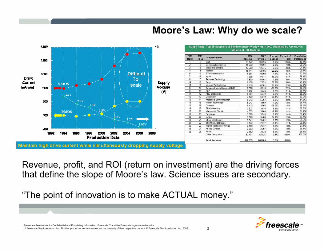
Moore’s Law: Why do we scale?
Revenue, profit, and ROI (return on investment) are the driving forces that define the slope of Moore’s law. Science issues are secondary.
“The point of innovation is to make ACTUAL money.”

TMFreescale Semiconductor Confidential and Proprietary Information. Freescale™ and the Freescale logo are trademarksof Freescale Semiconductor, Inc. All other product or service names are the property of their respective owners. © Freescale Semiconductor, Inc. 2008. 4
Moore’s Law: Scaling is difficult
We can ignore science issues, but they need to be addressed eventually!

TMFreescale Semiconductor Confidential and Proprietary Information. Freescale™ and the Freescale logo are trademarksof Freescale Semiconductor, Inc. All other product or service names are the property of their respective owners. © Freescale Semiconductor, Inc. 2008. 5
Simple view of a MOSFET

TMFreescale Semiconductor Confidential and Proprietary Information. Freescale™ and the Freescale logo are trademarksof Freescale Semiconductor, Inc. All other product or service names are the property of their respective owners. © Freescale Semiconductor, Inc. 2008. 6
Five problems with planar CMOS and their solutions:1. SOI or FINFET to reduce source/drain leakage (Ioff)2. Strain engineering to increase drive current (Ion)3. New silicide materials to reduce parasitic external resistance4. Metal oxides with high dielectric constants to reduce gate leakage5. Metal gate electrodes to reduce gate depletion (reduced EOT)
Five problems with planar CMOS
TMFreescale Semiconductor Confidential and Proprietary Information. Freescale™ and the Freescale logo are trademarksof Freescale Semiconductor, Inc. All other product or service names are the property of their respective owners. © Freescale Semiconductor, Inc. 2008. 7
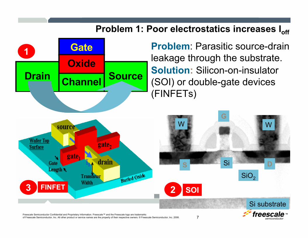
Problem 1: Poor electrostatics increases Ioff
Problem: Parasitic source-drain leakage through the substrate.Solution: Silicon-on-insulator (SOI) or double-gate devices (FINFETs)
Drain
Gate
Channel SourceOxide
1
3Si substrate
SiO2
S D
GWW
Si
2FINFET SOI

TMFreescale Semiconductor Confidential and Proprietary Information. Freescale™ and the Freescale logo are trademarksof Freescale Semiconductor, Inc. All other product or service names are the property of their respective owners. © Freescale Semiconductor, Inc. 2008. 8
Problem 2: Poor channel mobility decreases Ion
Rtot=Rext+RchRch scales with gate length (slope)Rext does not scale (offset)
450
500
550
600
0.030 0.035 0.040 0.045 0.050 0.055
Gate Length (um)
Rto
t (oh
m)
NiSi
Channel mobility limits Ion

TMFreescale Semiconductor Confidential and Proprietary Information. Freescale™ and the Freescale logo are trademarksof Freescale Semiconductor, Inc. All other product or service names are the property of their respective owners. © Freescale Semiconductor, Inc. 2008. 9
Enhanced channel mobility with stressor elements
Eg narrows
Conduction band valley
splitting
Valence band splitting
Mar
tin M
. Rie
ger a
nd P
. Vog
l Ph
ys.
Rev
. B 4
8, 1
4276
-142
87 (1
993)
Eg narrows
Conduction band valley
splitting
Valence band splitting
Eg narrows
Conduction band valley
splitting
Valence band splitting
Mar
tin M
. Rie
ger a
nd P
. Vog
l Ph
ys.
Rev
. B 4
8, 1
4276
-142
87 (1
993)
HolesHoles-Reduced interband hole-phonon scattering
-Reduced hole effective mass due to band warping
ElectronsElectrons-Reduced (f,g) intervalley electron-phonon scattering
-Preferential thermal population of electron states with light transport effective mass
Conduction Bands
Valence Bands
•Strain breaks the 6-fold conduction band valley degeneracy•Higher electron and hole mobilities•Better transport properties•Reduced intervalley scattering
•Biaxial tension lowers band gaps•Reduces effective masses•Splits bands/valleys
Four-fold in-plane valleys
Two-fold perpendicular valleys
Unstrained Si Strained Si on Si(1-x)Ge(x)
<100>
<001>
<010>

TMFreescale Semiconductor Confidential and Proprietary Information. Freescale™ and the Freescale logo are trademarksof Freescale Semiconductor, Inc. All other product or service names are the property of their respective owners. © Freescale Semiconductor, Inc. 2008. 10
SourceSource--Drain Stressor IntegrationDrain Stressor Integration
Gate Formation
Extension, Spacer, S/D Formation
Dopant Actication Anneal
Source-drain recess etch
Si:C or SiGe selective epitaxy
MEOL + BEOL Processing

TMFreescale Semiconductor Confidential and Proprietary Information. Freescale™ and the Freescale logo are trademarksof Freescale Semiconductor, Inc. All other product or service names are the property of their respective owners. © Freescale Semiconductor, Inc. 2008. 11
CMOS devices with process-induced stress
SiC:P SiC:Pchannel
Embedded source-drain stressors(1) SiGe:B for PMOS(2) Si:C:As for NMOS
NMOS
Tensile SiN
source drain
Gate
Stress memorization technique (SMT) - shownDual-stress liners (DSL) – not shownStressed silicon nitride layer to enhance mobility:(1) Compressive nitride for PMOS(2) Tensile nitride for NMOS

TMFreescale Semiconductor Confidential and Proprietary Information. Freescale™ and the Freescale logo are trademarksof Freescale Semiconductor, Inc. All other product or service names are the property of their respective owners. © Freescale Semiconductor, Inc. 2008. 12
Problem 3: Parasitic external resistance decreases Ion
Transition metal (Ti, Co, Ni, Pt, etc) silicides provide Ohmic contacts between the source-drain regions and the metal (W, Cu, Al) interconnects.Advantages of Nickel Silicide:
• Low Si consumption (92 Å of Si per 100 Å of Ni).• Diffusion-controlled reaction mechanism yields
uniform coverage, even in thin layers on narrow poly-Si lines.
• Low resistivity of NiSi (1.5 μΩcm). Disadvantages of Nickel Silicide:
• NiSi is metastable (NiSi2 forms at high temperatures).
• Fast diffusion of Ni in Si at low temperatures (~200°C).
• Agglomeration of thin NiSi films.
•Schottky barrier of 0.5 V for NFET and PFET.
Si substrate
SiO2
D S
GWW
Si

TMFreescale Semiconductor Confidential and Proprietary Information. Freescale™ and the Freescale logo are trademarksof Freescale Semiconductor, Inc. All other product or service names are the property of their respective owners. © Freescale Semiconductor, Inc. 2008. 13
Metal-Semiconductor Contacts: Schottky BarriersWork function: Distance from Fermi level to vacuum level. Most contacts are rectifying because of different work functions of the two materials.Work is needed (power wasted) for a carrier to cross this Schottky barrier (parasitic resistance).
Schottky barrier (Kittel)

TMFreescale Semiconductor Confidential and Proprietary Information. Freescale™ and the Freescale logo are trademarksof Freescale Semiconductor, Inc. All other product or service names are the property of their respective owners. © Freescale Semiconductor, Inc. 2008. 14
GdS
i2D
ySi2
HoS
i2YS
i1.7
YbSi
(?)
HfS
iZr
Si2
CrS
i2Ta
Si2
NbS
i2VS
i2
MnS
i
MoS
i2W
Si2
Ni2
SiN
iSi2
MnS
i1.7
FeSi
2C
oSi
Pd2S
iR
u2Si
3R
hSi
ReS
i2 OsS
i1.8
Ir2Si
3Pt
2Si IrS
iIrS
i3
ErSi
2
PtSi
NiS
i
TiSi
2 CoS
i2
0 .3
0.4
0.5
0.6
0.7
0.8
0.9
1.0
1.1
Barr
ier H
eigh
t on
n-ty
pe S
i (eV
)
conventionalCMOS
PMOSNMOS
Future CMOS devices will lose 20% of their power in the contacts.New materials for low-barrier contacts are crucial to reduce power.
Problem 3: Parasitic external resistance decreases Ion
PtSi for PMOS

TMFreescale Semiconductor Confidential and Proprietary Information. Freescale™ and the Freescale logo are trademarksof Freescale Semiconductor, Inc. All other product or service names are the property of their respective owners. © Freescale Semiconductor, Inc. 2008. 15
Problem 3: Use PtSi for PMOS contactsPMOS Performance Improved, NMOS degraded
Relative % change relative to NiSi
IonIoffPMOS 8.5%
-10
-9
-8
-7
-6
-5
-0.9 -0.8 -0.7 -0.6 -0.5PMOS Id,sat (A/mm)
log
[Ioff
(A/u
m)] Ni
Pt
35nm gate length100 nA/µm leakage1.2V Vdd
-9
-8
-7
-6
-5
0.6 0.7 0.8 0.9 1.0 1.1 1.2 1.3 1.4 1.5
NMOS Id,sat (A/mm)
NiPt
Relative % change relative to NiSi
IonIoffNMOS -9.0%
PMOS NMOS
Similar improvement for Id,lin and for PMOS devices with SiGe S/D stressors.

TMFreescale Semiconductor Confidential and Proprietary Information. Freescale™ and the Freescale logo are trademarksof Freescale Semiconductor, Inc. All other product or service names are the property of their respective owners. © Freescale Semiconductor, Inc. 2008. 16
Dual silicide process: PtSi for PMOS, NiSi for NMOS
Baseline CMOS flow to source-drain activation anneal
Pattern hardmask to cover NMOS
Pt deposition, anneal
Pt-PtSi selective etch
Remove oxide hardmask
Ni dep, anneal, selective etch
ILD0 module with etch stop stressors, back-end CMOS process
One additional mask:• PMOS has PtSi• NMOS unsilicided
N
P

TMFreescale Semiconductor Confidential and Proprietary Information. Freescale™ and the Freescale logo are trademarksof Freescale Semiconductor, Inc. All other product or service names are the property of their respective owners. © Freescale Semiconductor, Inc. 2008. 17
Problems 4/5: Gate leakage, Si/SiO2 charge depletion
Scaling:Channel doping increases (channel resistance, Debye length), requires higher gate capacitance to turn device off.Problem:Gate oxide thickness needs to shrink to turn the device off.Tunneling through the gate oxide leads to excess gate leakage.Solution:Use metal oxide (HfO2) with higher dielectric constant than SiO2.High-k gate dielectrics are expected to be introduced at the 45nm and32nm CMOS device generations.
Drain
Gate
Channel SourceOxide

TMFreescale Semiconductor Confidential and Proprietary Information. Freescale™ and the Freescale logo are trademarksof Freescale Semiconductor, Inc. All other product or service names are the property of their respective owners. © Freescale Semiconductor, Inc. 2008. 18
Gate leakage reduction by high-k oxides
10-7
10-6
10-5
10-4
10-3
10-2
10-1
10-0
10-1
5 10 15 20 25 30 35Equivalent Oxide Thickness (Å)
SiO2
High k
Less leakage
Lower power
Leak
age
Cur
rent
(A/c
m2 )
Ig limitFor wireless
Ig limitFor Logic
SiON
Use a thicker gate oxide with a higher dielectric constant to reduce leakage: Cox = kεoA/tox
k means ε, the low-frequency dielectric constant.
TMFreescale Semiconductor Confidential and Proprietary Information. Freescale™ and the Freescale logo are trademarksof Freescale Semiconductor, Inc. All other product or service names are the property of their respective owners. © Freescale Semiconductor, Inc. 2008. 19
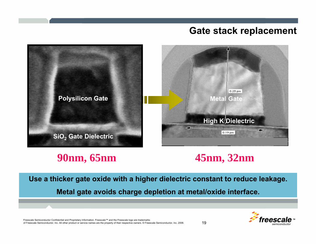
Gate stack replacement
45nm, 32nm
Metal Gate
High K Dielectric
Use a thicker gate oxide with a higher dielectric constant to reduce leakage.
Metal gate avoids charge depletion at metal/oxide interface.
90nm, 65nm
SiO2 Gate Dielectric
Polysilicon Gate

TM