nanomechanical testing of thin polymer films kyle maner and matthew begley structural and solid...
TRANSCRIPT

Nanomechanical Testing of Thin Polymer Films
Kyle Maner and Matthew Begley Structural and Solid
Mechanics Program Department of Civil Engineering University of Virginia
Uday Komaragiri (UVA) Special thanks to: Dr. Warren C. Oliver (MTS)
Prof. Marcel Utz (UConn)

Why test thin polymer films?
• Improve thermomechanical stability via self-assembly of nanostructure
• Establish connections between the nanostructure & mechanical properties
• Determine the size scale of elementary processes of plastic deformation
•Traditional nanoindentation of thin films bonded to thick substrates
• A novel freestanding film microfabrication procedure
• A novel method to probe freestanding films
Overview

Do polymers exhibit scale dependence?
Is traditional nanoindentation
sensitive enough to
detect such behavior?

3 Pure, amorphous polymers:
Poly(styrene) (PS) – Mw = 280 kD
Poly(methyl methacrylate) (PMMA) – Mw = 350 kD
Poly(phenylene oxide) (PPO) – Mw = 250 kD
2 Block co-polymers:
Poly(methyl methacrylate)-ruthenium (PMMA-Ru) – Mw = 56 kD (a metal-centered block co-polymer)
Poly(styrene)-poly(ethylene propylene) (PS-PEP) (a lamellar microphase separated block co-polymer)
Experimental Procedure
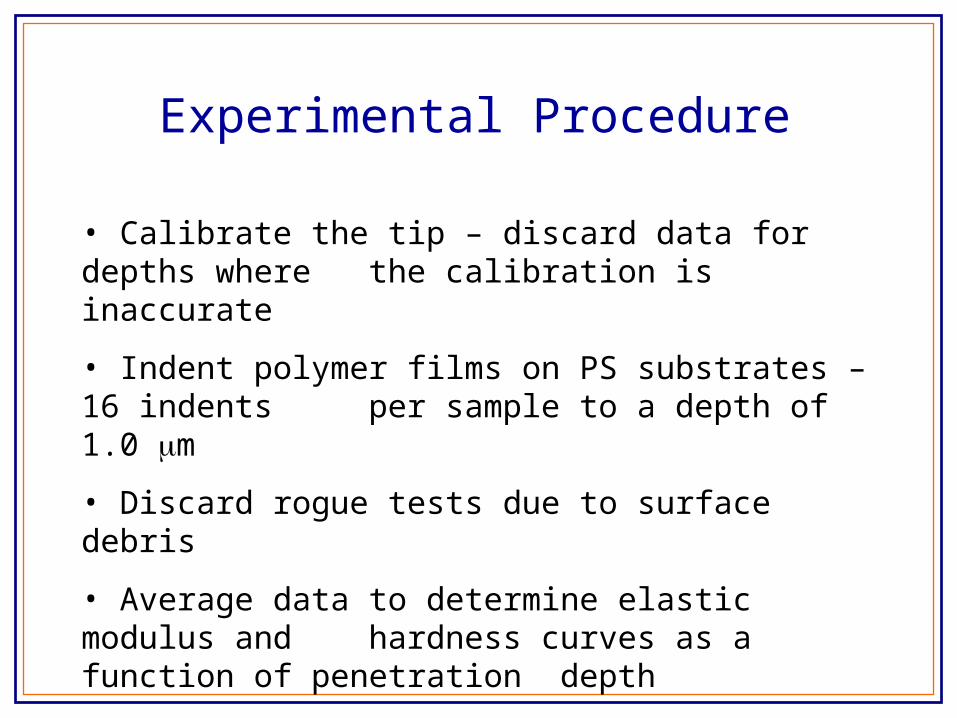
• Calibrate the tip – discard data for depths where the calibration is inaccurate
• Indent polymer films on PS substrates – 16 indents per sample to a depth of 1.0 m
• Discard rogue tests due to surface debris
• Average data to determine elastic modulus and hardness curves as a function of penetration depth

• The Berkovich diamond tip does not come to a perfect point
• The radius of the tip gradually increases with use
• The shape change alters the contact area of the indenter for a given depth
• A tip calibration determines the best-fit coefficients for the area function describing the tip
)()( 1
AECd
dPS r
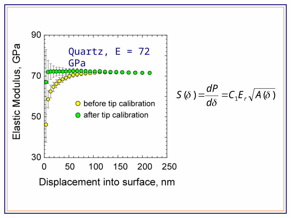
Quartz, E = 72 GPa
)()( 1
AECd
dPS r


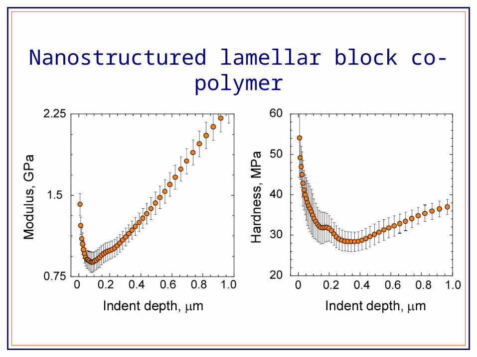
Nanostructured lamellar block co-polymer
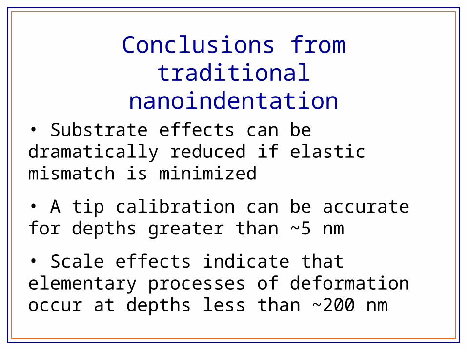
Conclusions from traditional nanoindentation
• Substrate effects can be dramatically reduced if elastic mismatch is minimized
• A tip calibration can be accurate for depths greater than ~5 nm
• Scale effects indicate that elementary processes of deformation occur at depths less than ~200 nm

• Traditional nanoindentation of thin films bonded to thick substrates
• A novel freestanding film microfabrication procedure
• A novel method to probe freestanding films
Overview

A new microfabrication procedure should be:
• applicable to a wide range of materials
• easily prepared on any wet-bench
• easily integrated with existing test equipment
• easily interpreted with relatively simple mechanics models
The experimental testing of the sample created should be:
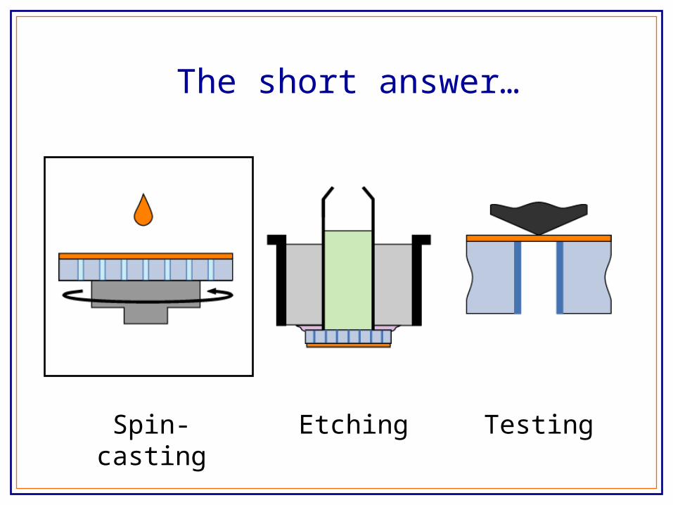
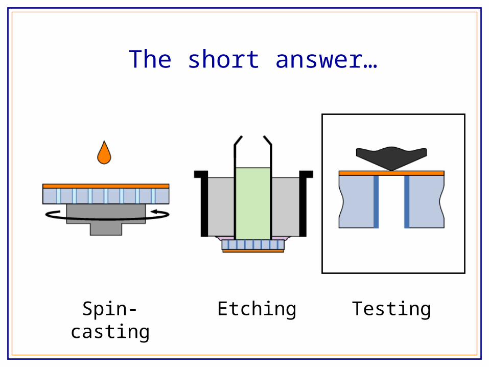
The short answer…
Spin-casting Etching Testing
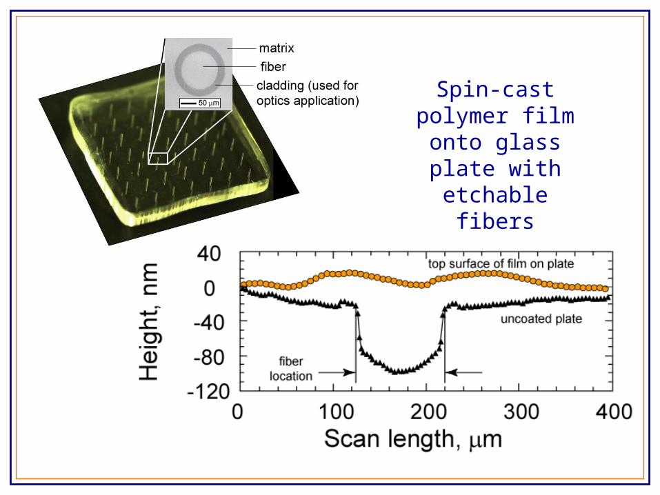
Spin-cast polymer film onto glass
plate with etchable fibers

The short answer…
Spin-casting Etching Testing
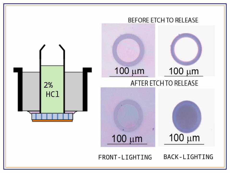
FRONT-LIGHTING BACK-LIGHTING
2% HCl
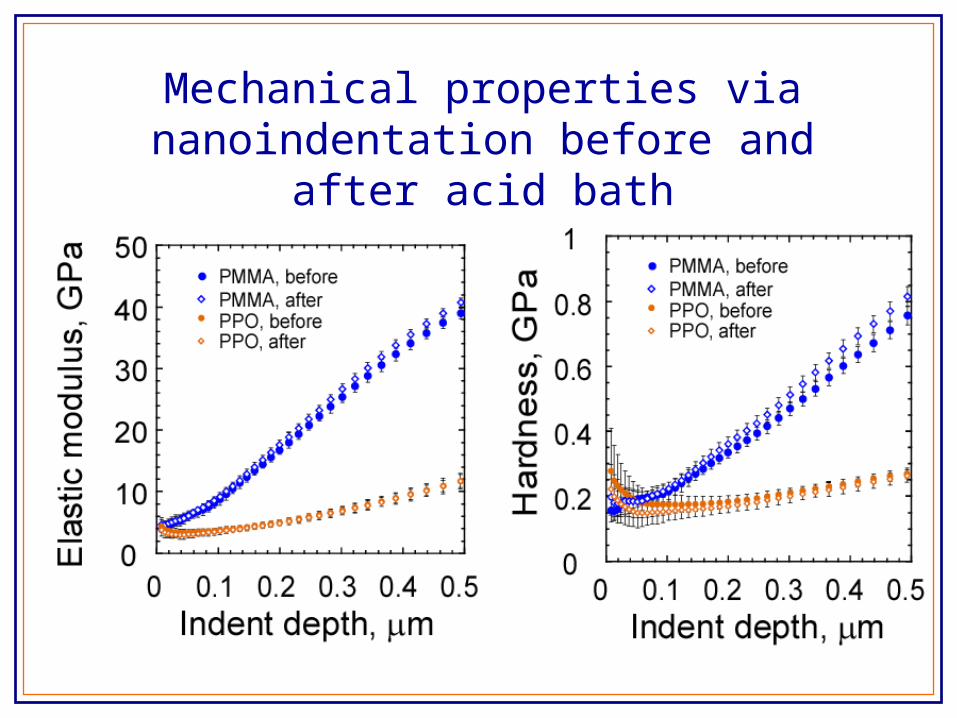
Mechanical properties via nanoindentation before and after acid bath
The short answer…
Spin-casting Etching Testing
•Traditional nanoindentation of thin films bonded to thick substrates
• A novel freestanding film microfabrication procedure
• A novel method to probe freestanding films
Overview

An overview of the test method
• constant harmonic oscillation superimposed on a ramp loading
• at contact, stiffness of sample causes drop in harmonic oscillation
• mechanical properties can be extracted from load-deflection response
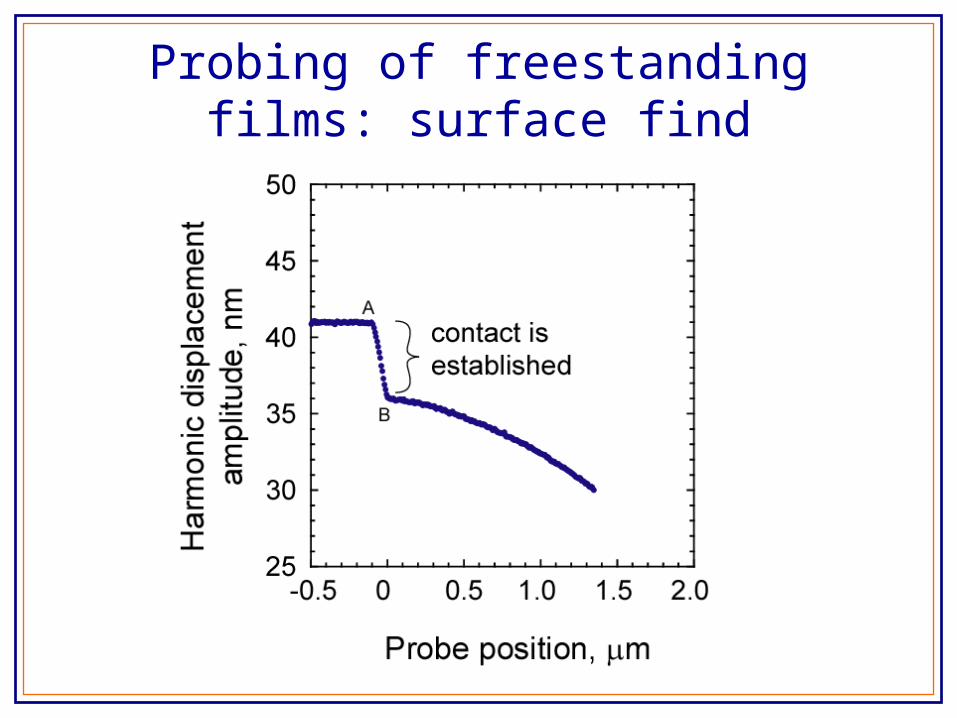
Probing of freestanding films: surface find

Probing of freestanding films: test flow


Stiffness scan

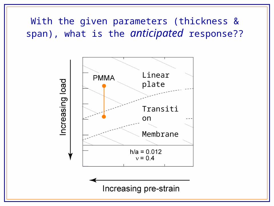
With the given parameters (thickness & span), what is the anticipated response??
Linear plate
Membrane
Transition

PMMA
Mw = 120 kD thickness = 350 nm span = 30 m
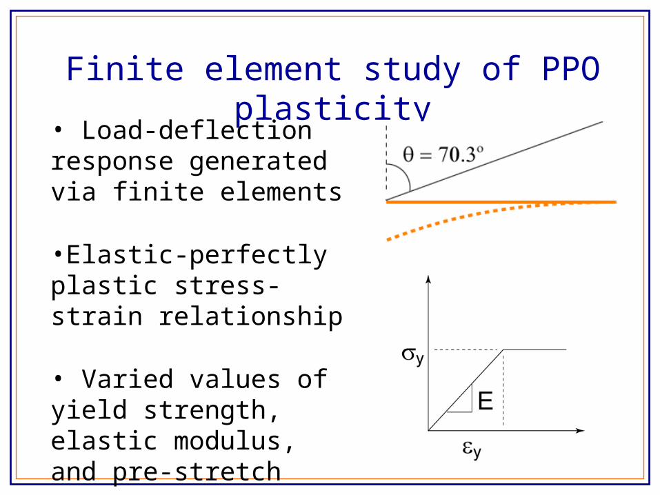
Finite element study of PPO plasticity
• Load-deflection response generated via finite elements
•Elastic-perfectly plastic stress-strain relationship
• Varied values of yield strength, elastic modulus, and pre-stretch
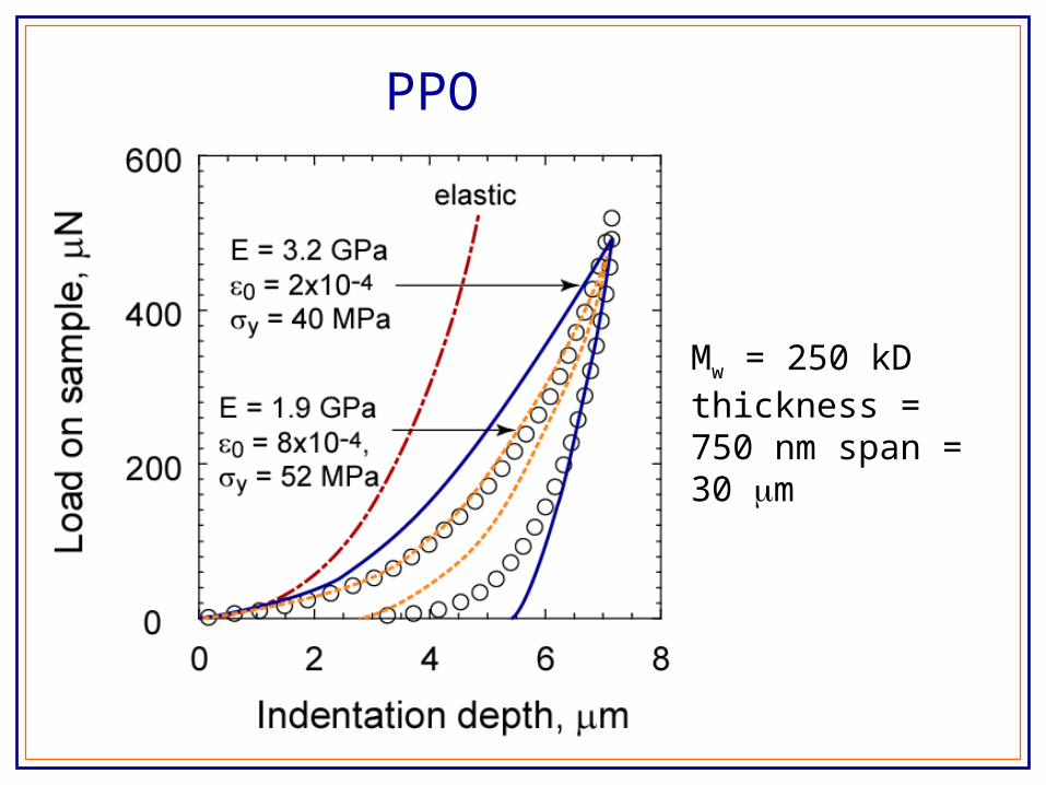
PPO
Mw = 250 kD thickness = 750 nm span = 30 m

Conclusions
• Approximated size scale over which elementary processes of plastic deformation occur in polymers
• Developed a new microfabrication technique to create submicron freestanding polymer films
• Developed a new testing method to probe thin freestanding films and illustrated its repeatability
• Successfully used numerical models to extract mechanical properties from submicron films

Questions?
Thank you.
• Introduction and motivation
• Description of the MTS Nanoindentation System
• Traditional nanoindentation of thin films bonded to thick substrates
• A novel freestanding film microfabrication procedure
• A novel method to probe freestanding films

Traditional methods of testing thin films
• Wafer curvature
• Bulge testing
• Nanoindentation of thin films bonded to thick substrates
• Microfabrication & probing of freestanding films

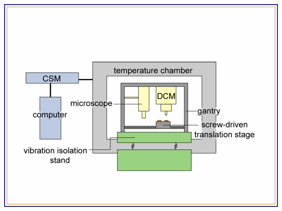
Nanoindentation Probe
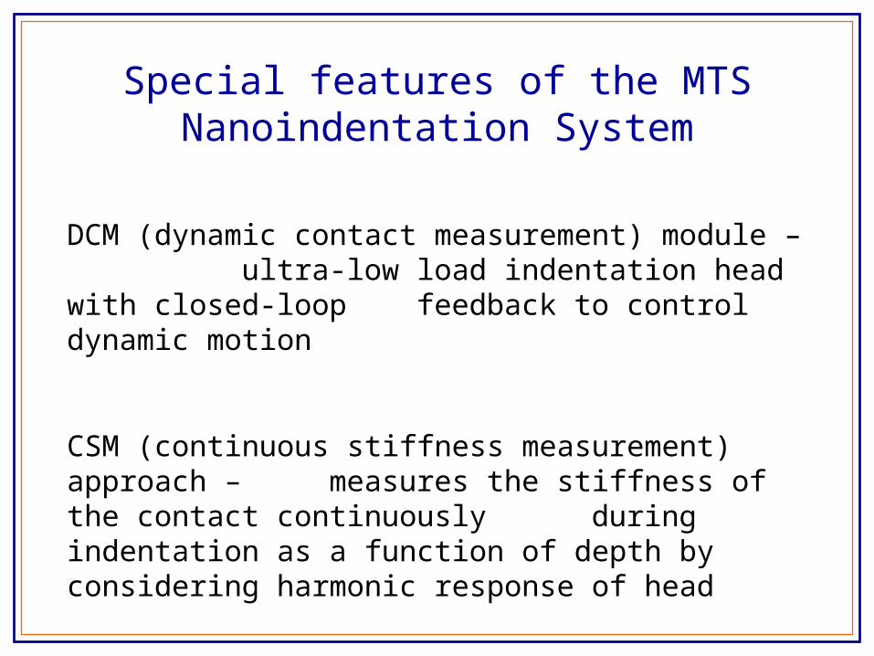
Special features of the MTS Nanoindentation System
DCM (dynamic contact measurement) module – ultra-low load indentation head with closed-loop feedback to control dynamic motion
CSM (continuous stiffness measurement) approach – measures the stiffness of the contact continuously during indentation as a function of depth by considering harmonic response of head

• Introduction and motivation
• Description of the MTS Nanoindentation System
• Traditional nanoindentation of thin films bonded to thick substrates
• A novel freestanding film microfabrication procedure
• A novel method to probe freestanding films

• Metals, metals, and more metals – deformation and scale-dependent behavior is well understood
• Plasticity in polymers – how it occurs but not how big
• Minimization of substrate effects via elastic homogeneity of film and substrate
• Probing of freestanding Si-based brittle and metal structures
The research on submicron films

The question of contact
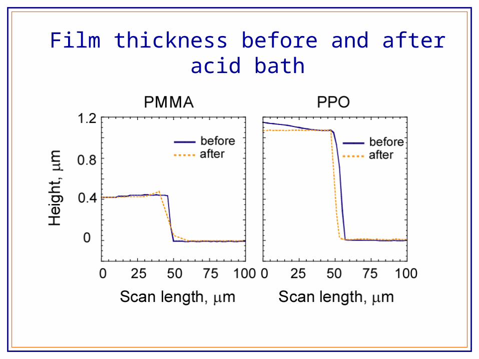
Film thickness before and after acid bath

A novel method to probe freestanding films should combat the problems facing
experimental testing of compliant films….
• Tip calibration errors can produce inaccurate measurements
•The surface of compliant materials is difficult to “find”
• Mechanics to extract properties is very complex
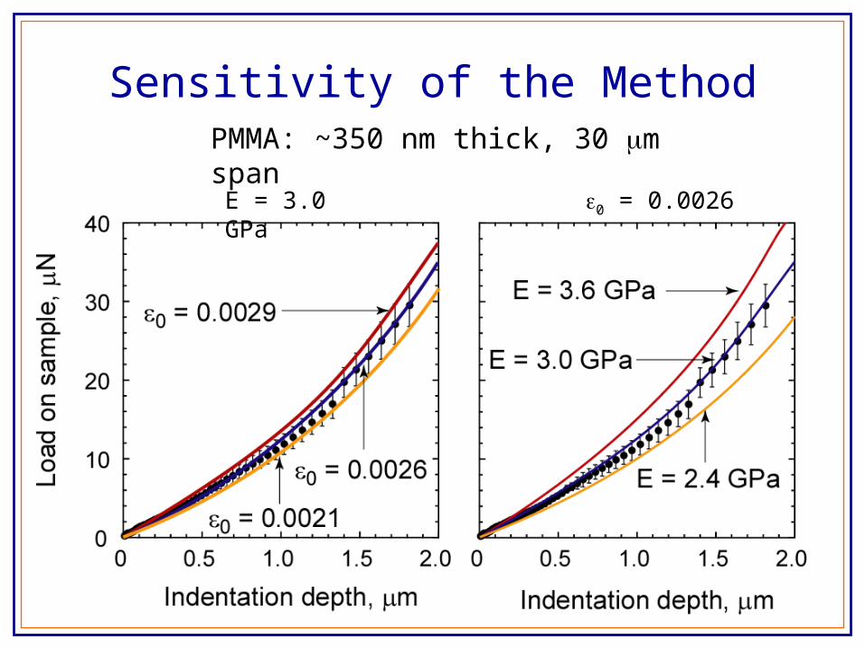
Sensitivity of the MethodPMMA: ~350 nm thick, 30 m span
E = 3.0 GPa 0 = 0.0026

Tip Calibration Equations
• Stiffness as a function of depth, S(), is measured
• The area function, A(), is determined from the following equation:
)(2
)(
AES r
• Elastic properties of calibration sample and indenter tip must be know to calculate, :rE
i
i
s
s
r EEE
22 111
• The calculated area function is a series with geometrically decreasing exponents:
...)( 2/132
21 CCCA

Standard method: Nanoindentation of film/substrate system
• CSM stabilizes harmonic motion of the indenter head
• Probe begins to move towards surface
• Contact (1) occurs when stiffness increases
• Load (2) to a prescribed displacement
• Hold (3) at maximum load to assess creep behavior
•Unload (4) 90% of the way
• Hold (5) at 90% unload to assess thermal drift

Parameters of Spin-Casting

Surface Characterizations
PS substrate
PMMA film on PS
substrate

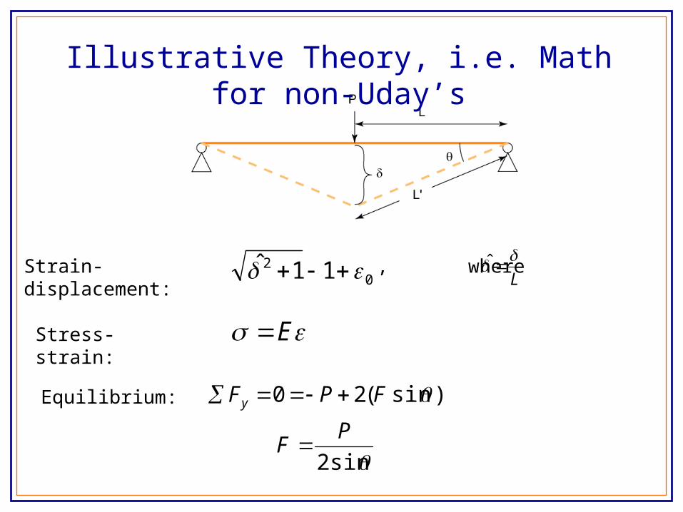
Illustrative Theory, i.e. Math for non-Uday’s
Strain-displacement:0
2 11ˆ
Stress-strain: E
Equilibrium:
sin2
)sin(20
PF
FPFy
L
ˆ, where

By combining the strain-displacement, stress-strain, and equilibrium equations, the following equation can be found:
ˆ
1ˆ
11ˆ
22
02
EAP
For small deflections, , thus:1ˆ ...)ˆ(0ˆ2
111ˆ 322
0
The equation for load becomes:
2
03
ˆ21
1
ˆ2ˆ
EAEAP
Due to small deflections, the denominator goes to 1, and load as a function of deflection is:
EAP )ˆ2ˆ()ˆ( 03
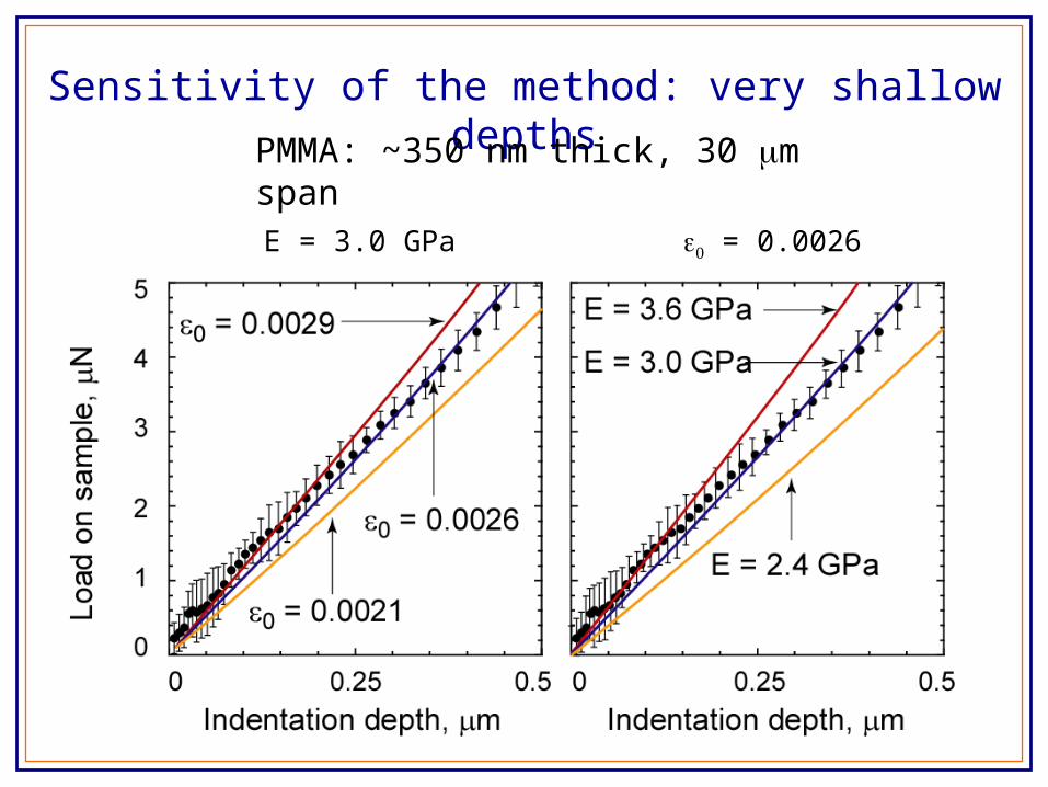
E = 3.0 GPa = 0.0026
Sensitivity of the method: very shallow depths
PMMA: ~350 nm thick, 30 m span