nano 101: exploring the nanoworld greta m. zenner university of wisconsin-madison materials research...
TRANSCRIPT

Nano 101:Exploring the Nanoworld
Greta M. ZennerUniversity of Wisconsin-Madison
Materials Research Science and Engineering Center on Nanostructured Interfaces
Troy DasslerAldo Leopold Elementary School

Outline
What
WhereWho
Why

Tata Nano
“Nano” All Around Us
Self-cleaning windows
Apparel with silver nanoparticles
Samsung washing machine Baby gear
VX Nano Cordless Laser Mouse

But what is nanotechnology?

Nanotechnology: Small, Different, New Federal definition (NNI)
Nanotechnology is the understanding and control of matter at dimensions of roughly 1 to 100 nanometers, where unique phenomena enable novel applications.
Encompassing nanoscale science, engineering and technology, nanotechnology involves imaging, measuring, modeling, and manipulating matter at this length scale.
Public definition1.The nanometer is extremely small. 2.At the nanometer scale, materials may behave differently. 3.We can harness this new behavior to make new technologies.

Nanometer:Part of The Metric System
kilometer km 1,000 1X10³
meter m 1 1X100
millimeter mm 1/1,000 1X10⁻³
micrometer m 1/1,000,000 1X10⁻⁶
nanometer nm 1/1,000,000,000 1X10⁻⁹
picometer pm 1/1,000,000,000,000 1X10-12

Size and Scale: Factors of 1000
meters
100
10-3m
illimeters
10-6m
icrom
eters
10-9
nan
om
etersHair: ~40 microns
Virus: 3-50 nm
Bacteria:3-5 microns
Courtesy of Dr. Charles Tahan
1 nm = 10 Hydrogen atoms:
DNA: 1-2 nm diameter

Nano Fun Fact
In the time it takes to read this sentence, your fingernails will have grown approximately one nanometer (1 nm).

So how small is a nanometer?
?
If you could paint a gallon of paint one nanometer thick, how much area would it cover?

Very, very, very small !!
A gallon of paint could cover the entire Arlington National Cemetery one nanometer thick.

Why Nanotechnology?

Smallness Leads to New Properties
ColorMelting point
StrengthConductivity
Reactivity
Nano GoldNano Aluminum
Bulk Aluminum
Bulk Gold

Big Potential = Jobs and Careers
Medical Applications
Information Technology
Energy Solutions
Water Desalination

Why Nano Education
Drawbacks
• Not inherently interesting
• Below visible threshold
• Unexpected properties• “Nano” not in the standards
– Although it can be integrated through all disciplines
Advantages
• Cutting-edge
• Future jobs and careers
• Fundamental science
• Breaks down disciplinary boundaries
• Fun!

Where is Nanotechnology?

Nanotechnology All around Us and Nanotechnology the Enabler
www.nanotechproject.org/inventories/consumer
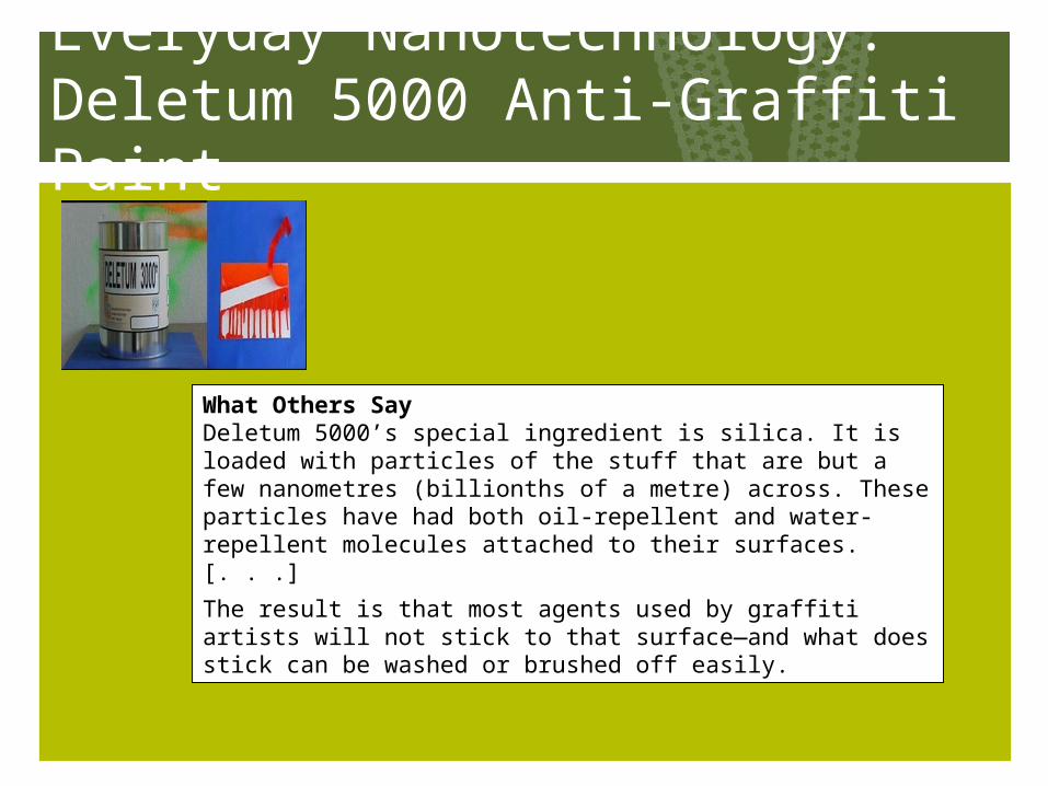
Everyday Nanotechnology:Deletum 5000 Anti-Graffiti Paint
What Others SayDeletum 5000’s special ingredient is silica. It is loaded with particles of the stuff that are but a few nanometres (billionths of a metre) across. These particles have had both oil-repellent and water-repellent molecules attached to their surfaces. [. . .]
The result is that most agents used by graffiti artists will not stick to that surface—and what does stick can be washed or brushed off easily.

A Lot Still in the Lab
Nancy Karuri
Karien Rodriguez
Bin Yang
Rachel Cannara
Brian Clare
Current and former graduate students at the University of Wisconsin

Nanotechnology’s Future: In Development

Nanotechnology’s Future?Deciding Where to Go

Who does nanotechnology?

An Interdisciplinary Endeavor
Nanoscience&
Nanotechnology
Engineering
Medicine
Biotechnology
Biology
Chemistry
Physics
Information Technology
Materials Science

An Interdisciplinary Endeavor
Nanoscience&
Nanotechnology
Engineering
Medicine
Biotechnology
Biology
Chemistry
Physics
Information Technology
Materials Science
SociologyEthics
Philosophy
Policy

Nanotechnology Research in Many Environments• Universities• Industries
– Large companies– Start-ups
• Government Labs• Range of educational
levels– Not just Ph.D.s!
• Range of disciplines– Including policy, art,
social sciences
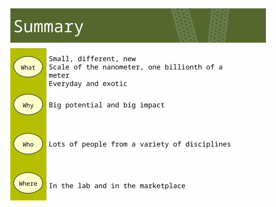
Summary
WhatSmall, different, newScale of the nanometer, one billionth of a meterEveryday and exotic
Why Big potential and big impact
Who Lots of people from a variety of disciplines
Where In the lab and in the marketplace

Acknowledgments
National Science FoundationNSF Nanoscale Informal Science Education Network (DRL-0532536)NSF Materials Research Science and Engineering Center on
Nanostructured Interfaces (DMR-0079983 and DMR-0520527)NSF Internships in Public Science Education (DMR-0120897 and
DMR-0424350)
NISE Net & UW MRSEC Personnel and Collaborators
Any opinions, findings and conclusions or recommendations expressed in this material are those of the author and do not necessarily reflect the views of the National Science Foundation (NSF).


How do researchers work at the nanoscale?
Scanning Probe Microscopy (SPM)

Scanning Probe Microscopy (SPM): “Feeling” a Surface
.
Path of tip
Tip
Atom Surface

SPM: Tip, Cantilever, Laser, Sensor, Computer

SPM: Measuring Properties
topography friction
Prof. Rob Carpick, University of Pennsylvania
50x50 µm2 imagesDiamond surface
sliding direction
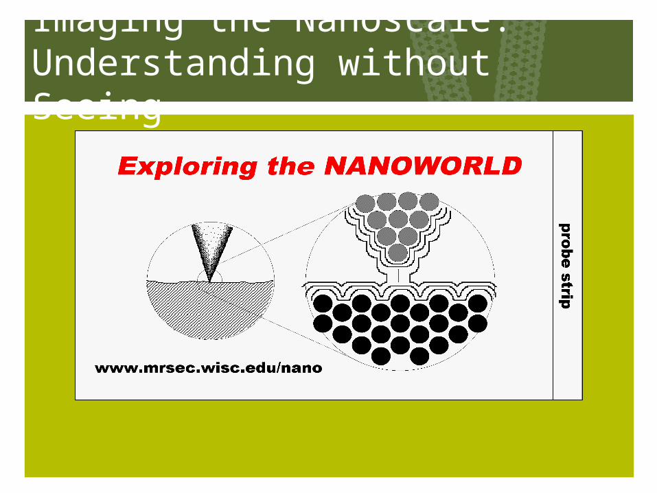
Imaging the Nanoscale:Understanding without Seeing

Imaging the Nanoscale:Understanding without Seeing
Pull Probe StripProbe
Sample
Pull Probe Strip
PR
OB
E
PROBE

(a) (b)
North South
(c)
Which best represents the poles?

SPM: Moving Atoms
Tip
Atom
Surface
Tunable bond

SPM: Moving Atoms into Quantum Corrals
IBM

Cool, but a Slow Way to Go

Self-Assembly

ReferencesSlide 5: Nano Not Widely Understood
– O.M. Castellini et al. Nanotechnology and the Public: Effectively Communicating Nanoscale Science and Engineering Concepts. Journal of Nanoparticle Research 9(2): 183-189 (2007)
– National Science Board. Science and Engineering Indicators 2008.
Slide 9: Nano Fun Fact, www.starling-fitness.com/wp-content/P1030148.jpg
Slide 11: Very, very, very small!, www.usconstitution.com/arlingtonnational.htm
Slide 22: Deciding where to go, en.wikipedia.org/wiki/Space_elevator
Slide 24-5: Who Does Nano, Based upon www.kuleuven.be/nanotechnology/taart.gif
Slide 25: Who Does Nano, pt 2, C. Miller et al., “Nanotechnology & Society: Ideas for Education and Public Engagement.” http://mrsec.wisc.edu/Edetc/society/nano_and_society.pdf
Slide 28: SPM: “Feeling,” G. Timp. Nanotechnology. 1999.
Slide 29: SPM: Measuring Properties, R. Carpick, UW/U Penn.
Slide 33: STM: Moving Atoms, G. Timp. Nanotechnology. 1999.
Slide 34: Quantum Corral, M.F. Crommie, C.P. Lutz, D.M. Eigler. Confinement of electrons to quantum corrals on a metal surface. Science 262, 218-220 (1993). www.ibm.com
Slide 35: IBM logo, D.M. Eigler, E.K. Schweizer. Positioning single atoms with a scanning tunneling microscope. Nature 344, 524-526 (1990). www.ibm.com
Slide 36: Self-Assembly, Cover. MRS Bulletin, Oct 2005; Cell membrane, http://library.thinkquest.org/C004535/cell_membranes.html; DNA, http://www.csb.yale.edu/userguides/graphics/ribbons/help/dna_rgb.html