muon detection in security applications and … velthuis, university of bristol 1/19 muon detection...
TRANSCRIPT

Jaap Velthuis, University of Bristol 1/19
Muon detection in security applications Muon detection in security applications Muon detection in security applications Muon detection in security applications and and and and
monolithic active pixel sensorsmonolithic active pixel sensorsmonolithic active pixel sensorsmonolithic active pixel sensors� Tracking in particle physics�Gaseous detectors� Silicon strips� Silicon pixels�Monolithic active pixel sensors�Cosmic Muon tomography�MAPS for Xray therapy� SPIDER� 3D vertical integration
Many thanks to those colleagues from who I Many thanks to those colleagues from who I Many thanks to those colleagues from who I Many thanks to those colleagues from who I ““““borrowedborrowedborrowedborrowed”””” pictures and resultspictures and resultspictures and resultspictures and results

Jaap Velthuis, University of Bristol 2/19
LHCLHCLHCLHC� 27 km long circular
accelerator 100m under ground in Geneva
� Protons are accelerated up to 7TeV and collided at couple of locations along beam line Here giant detectors are built
� Take digital pictures and decide whether they interesting or not every 25 ns
� Particle Physics:• Very fast imaging with
very precise sensors• Very fast processing of
large data sets

Jaap Velthuis, University of Bristol 3/19
Detection conceptDetection conceptDetection conceptDetection concept
�Most of the tracking detectors in particle physics exploit local ionisation• A charged particle passes
through the detector and due to Coulomb interaction a current pulse is generated
• The charge is measured on various signal wires
• Particle position is reconstructed by weighting charge

Jaap Velthuis, University of Bristol 4/19
Gaseous wire chambersGaseous wire chambersGaseous wire chambersGaseous wire chambers
�Here the detection medium is gas
�Charge induces signal on a couple of wires
� Issues:• Wires are very long (here
2.4m)• Need large distances between
the wires• Need a lot of energy to ionise
an atom• Charge travels slowly
Jaap Velthuis, University of Bristol 5/19
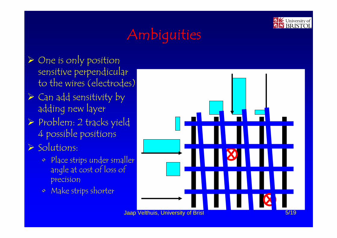
AmbiguitiesAmbiguitiesAmbiguitiesAmbiguities
� One is only position sensitive perpendicular to the wires (electrodes)
� Can add sensitivity by adding new layer
� Problem: 2 tracks yield 4 possible positions
� Solutions: • Place strips under smaller
angle at cost of loss of precision
• Make strips shorter
X
X

Jaap Velthuis, University of Bristol 6/19
Silicon stripsSilicon stripsSilicon stripsSilicon strips
� In silicon sensors one can:• Make shorter strips
(~6cm per wafer)• Place them closer
together
� Additional benefits:• Charge travels fast• Sensors can be thin
(typically 300µm)• Mechanically easier to
handle

Jaap Velthuis, University of Bristol 7/19
Silicon pixelsSilicon pixelsSilicon pixelsSilicon pixels
� Even shorter strips: pixels
� Every pixel has own readout circuit
�Connected using flip-chip bump bonding• ATLAS: 50x400 µm2
• CMS: 100x150 µm2
� Still separate wafers for electronics and sensor
Jaap Velthuis, University of Bristol 8/19
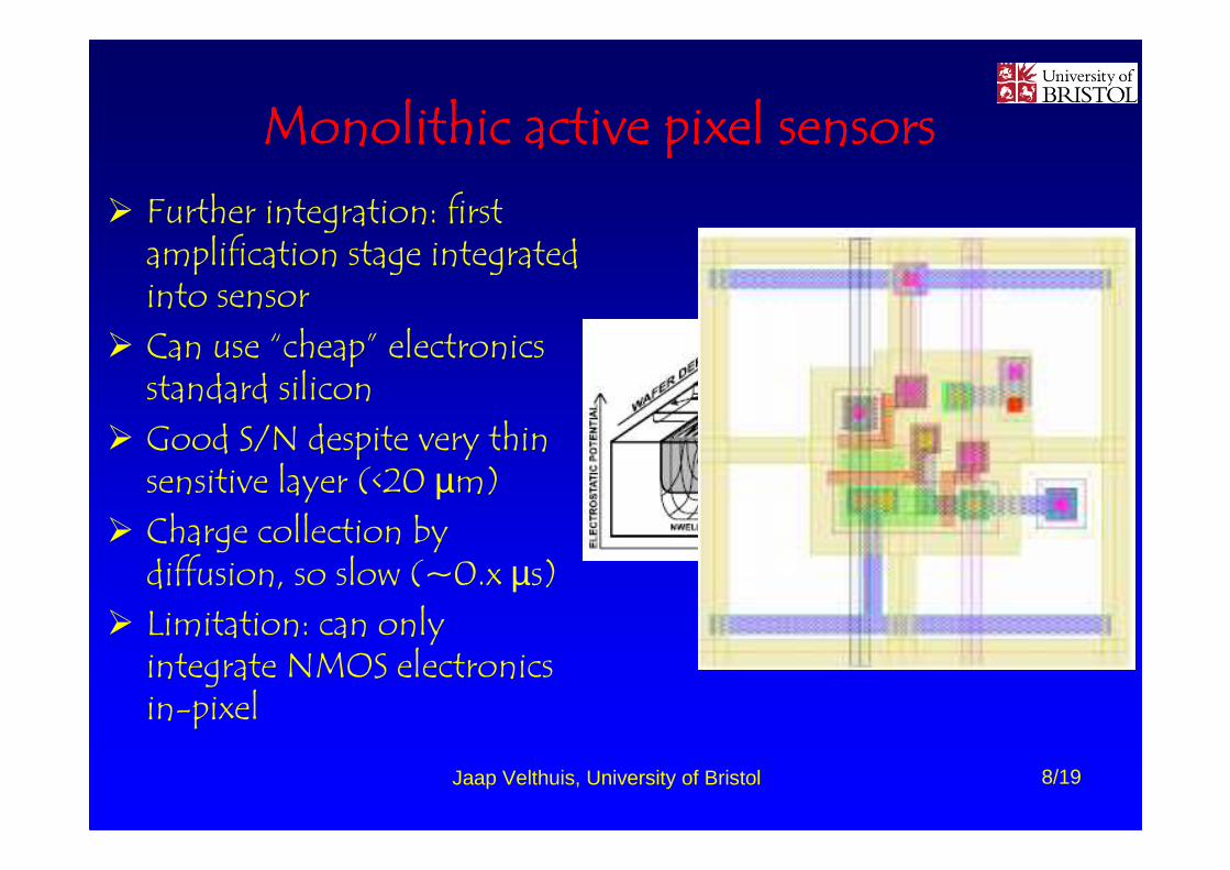
Monolithic active pixel sensorsMonolithic active pixel sensorsMonolithic active pixel sensorsMonolithic active pixel sensors
� Further integration: first amplification stage integrated into sensor
� Can use “cheap” electronics standard silicon
� Good S/N despite very thin sensitive layer (<20 µm)
� Charge collection by diffusion, so slow (~0.x µs)
� Limitation: can only integrate NMOS electronics in-pixel

Jaap Velthuis, University of Bristol 9/19
Some examplesSome examplesSome examplesSome examples
�We are currently working on two applications of particle physics sensors• Cosmic ray tomography• MAPS for Xray therapy
� State-of-the-art: INMAPS

Jaap Velthuis, University of Bristol 10/19
Cosmic Ray tomographyCosmic Ray tomographyCosmic Ray tomographyCosmic Ray tomography� Are developing high resolution
Resistive Plate Chambers for Cosmic Ray tomography• Planes ~1x1m2, strips 1.5mm apart
� Idea: • compare track of cosmic muon before
entering and after exiting a volume• If muon hits material it will scatter• Scattering depends on the material
� Advantages:• RPCs cheap and easy to make in large
areas• Muons are highly penetrating• Muons are naturally occurring so
impossible to trigger against• Many channels but due to multiplexed
readout not a problem� Takes ~30 sec to find tennisball size
object in a suitcase volume
FeU
CH Al

Jaap Velthuis, University of Bristol 11/19
MAPS for XMAPS for XMAPS for XMAPS for X----ray therapyray therapyray therapyray therapy� Issue in Xray therapy: dose verification� Currently, many calibration measurements
needed• Water phantom placed in position of the
patient and absorbed dose measured, then patient undergoes therapy
� Measurements during irradiation difficult• Do not want to disturb beam upstream of
patient• Patient scatters too much to measure
downstream� These measurements are getting more
important as the novel trend is to use multi-leaf collimators to make very precise thin beams (Intensity Modulated Radiation Therapy)
� PTW recently introduced the DAVID, multi-wire ionization chamber to monitor the dose in real time
• All wires parallel thus information only 1 dimensional
• Since many interactions, not possible to add second layer

Jaap Velthuis, University of Bristol 12/19
MAPS for MAPS for MAPS for MAPS for XrayXrayXrayXray therapytherapytherapytherapy
� MAPS can be very thin (<25µm) with still very good S/N
� Can use this to measure the dose in real 2D and really in real-time.• Frame rates of 40 per second with
6x6cm2 sensors (16Mpix) have been demonstrated
• Can go up to ~10Gpix/sec� Here collimated beam and sensor read
out 8 frames per second• Added 15 cm Pb• Slice parallel to X-axis shows know
where beam is better than 60µm• Improving cuts yields 50µm
� Looking for funding and/or industrial partner to take this forward

Jaap Velthuis, University of Bristol 13/19
Towards intelligent pixelsTowards intelligent pixelsTowards intelligent pixelsTowards intelligent pixels� Limitation: can only
integrate NMOS electronics in-pixel
� PMOS transistors need Nwell. This Nwell competes with diode for charge. If can live with 25-50% signal can now make intelligent pixels• Pixel size: 30x30µm2
• Per pixel: two 8-bit DRAM cells, one 8-bit ROM cell and one 1-bit DRAM
• Forms ADC in-pixel with hit flag
• Can store one event while processing another

Jaap Velthuis, University of Bristol 14/19
SPIDER: taking MAPS to the next levelSPIDER: taking MAPS to the next levelSPIDER: taking MAPS to the next levelSPIDER: taking MAPS to the next level� In SPIDER we are taking MAPS
to the next level using INMAPS process
� Problem in MAPS:• PMOS electronics need Nwell• Nwell acts as charge collection
diode• So can’t make PMOS without
losing huge amount of Q
� New development: make deep pwell with Nwell inside → can do CMOS with no charge loss• Road to data processing in pixel for
small signals

Jaap Velthuis, University of Bristol 15/19
The SPIDER future: CherwellThe SPIDER future: CherwellThe SPIDER future: CherwellThe SPIDER future: Cherwell�Uses INMAPS plus 4T to achieve:
• 100% fill factor with integratedsensor and readout electronics
• Incorporation of complex logic within a in series of pixels
• Investigation of data reduction/clustering• Low noise using transfer gate, CDS and
in-pixel amplification• Low power using rolling shutter readout• First prototype submitted. Has ADC in
islands
� This can be the next generation intelligent detector for Particle Physics
4
TSELECT
CO
L
RESET
4
T
CO
L
4
T
CO
L
50 um pixel
boundary
1x
SRAM
4
TSELECT
CO
L
RESET
4
T
CO
L
4
T
CO
L
50 um pixel
boundary
1x
SRAM
Pixel
Bo
un
dary
BIAS
CO
L
VTH
MEMORY [0]
MEMORY [1]
MEMORY [2]
MEMORY [3]
MEMORY [4]
MEMORY [5]
MEMORY [6]
MEMORY [7]
Co
ntr
ol
log
icC
on
tro
l lo
gic
WrEn
TRIM
(CDS circuit)
CRCS
+ -∑
BIAS
CO
L
VTH
MEMORY [0]
MEMORY [1]
MEMORY [2]
MEMORY [3]
MEMORY [4]
MEMORY [5]
MEMORY [6]
MEMORY [7]
Co
ntr
ol
log
icC
on
tro
l lo
gic
WrEn
TRIM
(CDS circuit)
CRCS
+ -∑

Jaap Velthuis, University of Bristol 16/19
3D integration3D integration3D integration3D integration� Technology for the day after
tomorrow� Multi-layer devices new trend
chip industry• Make chips faster by minimizing
distance between components
� Processing each layer can be optimised
� Technologies can be mixed (e.g. 0.09 CMOS on 0.25 CMOS mixed mode)
� Concept “simple”: • make chip for 1 layer• Thin down to remove excess Si• Place on top and make
connections
Opto Electronics
and/or Voltage Regulation
Digital Layer
Analog Layer
Sensor Layer
Physicist’s Dream
50 um
Power In
Optical In Optical OutPhoto from MIT LL
Six inch wafer thinned to 6 microns and mounted on 3 mil kapton.

Jaap Velthuis, University of Bristol 17/19
3D integration example3D integration example3D integration example3D integration example� 3D Laser rader imager
• 64x64 array, 30µm pixels• 3 tiers
� 0.18µm SOI� 0.35 µm SOI� High resistivity substrate diodes
� Oxide to oxide wafer bonding� 1.5µm vias� dry etch� 6 3D vias/pixel

Jaap Velthuis, University of Bristol 18/19
SummarySummarySummarySummary
� In Particle Physics the challenges are to make very fast, very large detector arrays of tiny detector elements with very fast processing
� The technology developed can also be used for various other applications like:• Security• Medicine
� INMAPS the way forward. Watch this space, exciting developments ahead

Jaap Velthuis, University of Bristol 19/19
AcknowledgementsAcknowledgementsAcknowledgementsAcknowledgements� Many thanks go to
• My colleagues at the University of Bristol• My colleagues of the SPIDER collaboration (slide 14&15)
• My colleagues of the CMOS Sensor Design group at RAL (slide 13&14)
• My colleagues at AWE (slide 10)
• My colleagues at Bristol Hospital and Dr Hugtenburg (Swansea) (slide 11&12)
� I “borrowed“ pictures from• CERN/ATLAS/CMS (slide 2&7)
• ZEUS collaboration (slide 4&6)
• LEPSI/Strasbourg on MIMOSA (slide 8)
• Ray Yarema (Fermi lab) on 3D integration (slide 16&17)