multimodal cantilevers with novel piezoelectric layer ... · multimodal cantilevers with novel...
TRANSCRIPT

358
Multimodal cantilevers with novel piezoelectric layer topologyfor sensitivity enhancementSteven Ian Moore*, Michael G. Ruppert and Yuen Kuan Yong
Full Research Paper Open Access
Address:The School of Electrical Engineering and Computer Science, TheUniversity of Newcastle, Callaghan NSW 2308, Australia
Email:Steven Ian Moore* - [email protected];Michael G. Ruppert - [email protected];Yuen Kuan Yong - [email protected]
* Corresponding author
Keywords:atomic force microscopy; multifrequency AFM; multimodal AFM;piezoelectric cantilever, self-sensing
Beilstein J. Nanotechnol. 2017, 8, 358–371.doi:10.3762/bjnano.8.38
Received: 07 October 2016Accepted: 17 January 2017Published: 06 February 2017
This article is part of the Thematic Series "Advanced atomic forcemicroscopy".
Guest Editor: T. Glatzel
© 2017 Moore et al.; licensee Beilstein-Institut.License and terms: see end of document.
AbstractSelf-sensing techniques for atomic force microscope (AFM) cantilevers have several advantageous characteristics compared to the
optical beam deflection method. The possibility of down scaling, parallelization of cantilever arrays and the absence of optical
interference associated imaging artifacts have led to an increased research interest in these methods. However, for multifrequency
AFM, the optimization of the transducer layout on the cantilever for higher order modes has not been addressed. To fully utilize an
integrated piezoelectric transducer, this work alters the layout of the piezoelectric layer to maximize both the deflection of the canti-
lever and measured piezoelectric charge response for a given mode with respect to the spatial distribution of the strain. On a proto-
type cantilever design, significant increases in actuator and sensor sensitivities were achieved for the first four modes without any
substantial increase in sensor noise. The transduction mechanism is specifically targeted at multifrequency AFM and has the poten-
tial to provide higher resolution imaging on higher order modes.
358
IntroductionThe invention of the atomic force microscope (AFM) [1] provi-
ded for the observation of the nanoscale like no other tool
before it [2]. The technologies derived from research into the
AFM have led to developments in nanomachining [3], nanome-
trology [4], material science [5], semiconductor manufacturing
[6,7] and high-density data storage systems [8-10].
The AFM uses a sharp probe tip at the free end of a cantilever
to interrogate and image the surface of a sample [11-13]. When
using the AFM in dynamic mode [14], the cantilever is excited
at its fundamental modal frequency and the probe lightly taps
the surface of the sample. Observed changes in the amplitude,
phase or frequency shift of the cantilever’s motion correlate to
properties of the sample [15]. When closing a feedback loop
around these observables with the z-axis nanopositioner, the
controller output is routinely used to map the surface topogra-
phy of the sample. Recently, the additional excitation and detec-
tion with multiple frequencies has led to vast improvements in

Beilstein J. Nanotechnol. 2017, 8, 358–371.
359
the nanomechanical characterization of the sample beyond it’s
topography [16]. For these multifrequency AFM (MF-AFM)
methods, higher order modes provide enhanced imaging proper-
ties such as higher modal stiffnesses and faster response times.
It was shown that these higher modes can be more sensitive to
material properties such as elastic modulus and damping coeffi-
cients [17-19]. Additionally, stiff cantilevers have proven to
provide high resolution imaging in ambient and liquid environ-
ments using quartz resonators [20,21].
Traditional AFM cantilever instrumentation requires a piezo-
electric stack actuator at the base of the cantilever for excitation
[3] inevitably adding additional resonances as is visible from
the so called forest of peaks [22]. These additional frequency
components make cantilever resonance tuning almost impos-
sible in liquids [23,24] and can alter the cantilever response
rendering the identification and subsequent analysis of higher
modes exceedingly difficult. For this reason, numerous inte-
grated actuation methods such as magnetic [25], photothermal
[26], resistive thermal [27], ultrasonic [28] or via a piezoelec-
tric layer [29] have been devised.
In order to measure the cantilever deflection, the optical beam
deflection (OBD) method [30] is still the widely used standard.
However, the measurement setup for the OBD method has limi-
tations, such that it requires frequent laser alignment, a cantile-
ver with a reflective surface and a certain minimum dimension
as dictated by the laser spot size. Further, the method suffers
from imaging artifacts due to optical interferences originating
from stray light reflected by the sample surface [31,32] and
bandwidth limitation of the readout circuit [33]. In contrast, a
strain-based deflection measurement offers several advantages
including a much more compact measurement setup, potential
for scalability to cantilever arrays as well as increased sensi-
tivity for smaller cantilever dimensions [34-38].
Among the existing integrated actuation and sensing methods,
piezoelectric transduction seems to be the only one capable of
simultaneously serving as an actuator and a sensor even with a
single active layer [39,40]. A set of cantilever designs exist
which integrate a piezoelectric transducer onto the cantilever as
part of the microfabrication process [41]. While good imaging
performance is achieved when operating these cantilevers at
higher order modes, the topology of the piezoelectric layer is
designed with no consideration of the modal response of the
cantilever.
A number of researchers have investigated shaping the piezo-
electric layer to actuate or sense a single mode of beam and
plate structures whilst filtering the responses of the other modes
[42-46]. The design of these transducers, denoted modal
sensors/actuators, encompasses the modeling and modal analy-
sis of the structure in order to determine the modal frequencies
and deflection mode shapes. Here, the overall deflection is the
linear combination of mode shapes which have a fixed spatial
distribution. Moreover, there exists a linear mapping from the
deflection of the structure to the charge developed on the piezo-
electric layer and hence the charge response is related to the
spatial distribution of each mode shape. If the mode shapes are
orthogonal, an analytical approach can be used to shape the
piezoelectric layer. Otherwise optimization is used to shape the
piezoelectric layer to minimize response to the undesired
modes.
This work formulates the design of the topology of the piezo-
electric layer on an AFM cantilever to maximize the actuator
gain and sensor sensitivity with respect to the cantilever’s
higher order modes. Compared to previous work on modal
sensor/actuators [42-46], the design specification of the
presented work is to enhance the desired modes rather than
suppress the undesirable modes. This difference leads to funda-
mental changes in the design strategy, resulting piezoelectric
layer topology, instrumentation, actuator characteristics and
sensor characteristics. Indeed, the justification for this altered
approach comes from the fundamental reasons for multifre-
quency AFM which is based on the assumption that additional
information is encoded in these higher modes. To enable the op-
timization of the piezoelectric response to higher order modes,
plate theory with finite element analysis is used to determine the
spatial distribution and polarity of the transducers response for a
given mode shape. Using this result, the piezoelectric layer is
split into isolated regions whose individual responses construc-
tively combine in order to maximize the actuator gain/sensor
output.
The remainder of the paper is organized as follows. Section
’Modal analysis of the piezoelectric cantilever’ outlines the
modeling approach to determine the spatial charge distribution
of the piezoelectric transducer as a function of its modal
response. In section ’Proposed piezoelectric cantilever designs’,
results of this analysis are used to determine the design of the
piezoelectric actuator arrangements to maximize the transducer
response for the first four modes of a cantilever with a stepped
geometry. In section ’Instrumentation of the cantilever’ the
working principle and modeling of the instrumentation is
presented. The experimentally determined actuator and sensor
transfer functions are presented in section ’Experimental
Results’, which highlight the actuator gain and sensor sensi-
tivity improvements of the proposed designs. In addition, this
section presents and discusses the noise characterization of the
sensor. The cantilever designs presented in this work target a
single mode each. Section ’Instrumentation for multifrequency

Beilstein J. Nanotechnol. 2017, 8, 358–371.
360
AFM’ outlines a method to design and instrument the cantile-
vers to target multiple modes.
Results and DiscussionModal analysis of the piezoelectric cantileverFigure 1 shows the silicon cantilever analyzed in this work. The
dimensions in the diagram are stated in Table 1. The benefit of
the stepped geometry of the cantilever is that higher modes are
more closely spaced compared to rectangular cantilevers
[47,48] and higher mode deflections are amplified [49] which
benefits higher harmonic/higher mode applications [41].
Figure 1: The dimensions of the basic cantilever design. The grayzone is the piezoelectric layer. The zoomed in section of a plate showsthe out of plane deflection w and the rotation of the normal of the canti-lever’s neutral plane (N.P.) about the y-axis θy. The rotation of thenormal of the cantilever’s neutral plane about the x-axis θx is equiva-lent to θy for a section in the yz-plane. The fixed boundary of the canti-lever is shown to the left of the image.
Table 1: Cantilever dimensions shown in Figure 1.
Parameter Value
l1 400 μml2 400 μmw1 100 μmw2 500 μmh 10 μm
The cantilever is modeled using Mindlin plate theory and a
finite element (FE) model is developed to perform modal analy-
sis [50,51]. Modal analysis using the FE model provides a solu-
tion to the out-of-plane deflection w(x,y,t) and the rotations of
the normal of the cantilever’s neutral plane around the x-axis
and y-axis, θx(x,y,t) and θy(x,y,t) respectively. These quantities
are shown in Figure 1. Assuming a thin piezoelectric layer, the
response of the piezoelectric transducer is proportional to the
strain at the surface of the cantilever. The in-plane strains at the
surface of the cantilever are [51]
(1)
(2)
(3)
The electrodes are uniformly distributed on both sides of the
piezoelectric layer to generate electric fields only in the z-axis.
Therefore, the electric displacement in the piezoelectric materi-
al is [52]
(4)
where d31, d32 and d36 are the piezoelectric coefficients.
Assuming the piezoelectric material is poled along the z-axis
and is homogeneous, the coefficients d31 = d32 = d and d36 = 0
[52,53]. The charge produced is the integral of the electric dis-
placement, that is
(5)
(6)
The domain Ω is the area of the piezoelectric layer.
Modal analysis with the FE model evaluates harmonic solu-
tions for θx and θy of the form
(7)
(8)
The spatial functions (x,y) and (x,y) are the mode shapes
of cantilever.
In the following analysis, the domain Ω from Equation 5 is
restricted to the domain Ae of a single rectangular element from
the mesh used in the FE model. The modal analysis calculates
the rotations and at the four nodes of the element. The
mode shapes over an element are

Beilstein J. Nanotechnol. 2017, 8, 358–371.
361
(9)
(10)
where N(x,y) are the shape functions [50,51]
(11)
where the dimensions of the rectangular element are 2a× 2b and
the origin is placed at the center of the rectangular element.
By substituting the harmonic solution into Equation 5 the
charge response of the piezoelectric transducer over the ele-
ment is
(12)
where
(13)
Be represents the response due to the spatial nature of the piezo-
electric layer in the xy-plane for a given mode. This expression
is evaluated using Gaussian quadrature. Since the shape func-
tions are quadratic, the derivatives are linear. This allows the
exact integral to be evaluated with Gaussian quadrature at the
midpoint of the rectangular element. Evaluating Be for each ele-
ment over the entire cantilever provides the charge response for
a given mode.
Proposed piezoelectric cantilever designsThe aim of the proposed cantilever designs is to increase the
actuator gain and sensor sensitivity of the piezoelectric trans-
ducer to flexural and torsional modes. First, using the finite ele-
ment method, modal analysis is performed on the cantilever
topology shown in Figure 1 to calculate the mode shapes. For
mode 1 to mode 4 (M1–M4), the simulated mode shapes of the
cantilever are shown in Figure 2a–d. The modal frequencies are
38.3 kHz, 119 kHz, 176 kHz, and 342 kHz. M1, M2 and M4 are
flexural modes while M3 is a torsional mode. The modal analy-
sis provides the mode shapes for the deflection and rotations at
the nodes of the FE mesh. Using these values, the quantity Be is
calculated for each element in the mesh.
If the sign of Be for two elements are the same, the response
over the two elements adds constructively. If of opposite sign,
the response over the two elements adds destructively. Based on
the sign of Be, the piezoelectric layer is split into two, denoted
the positive and negative transducer. By actuating and sensing
each separately and combining the responses with opposite
polarities, the combination of responses is purely constructive.
This improves the actuation and sensing by the transducer to its
targeted mode.
This design procedure can be posed as an optimization problem.
For the i-th finite element in the cantilever mesh, the associated
Be is denoted The piezoelectric material on each finite ele-
ment is observed in either a positive polarity or negative
polarity. A design parameter is introduced indicat-
ing this polarity. If χi = 1 the finite element is part of the posi-
tive transducer otherwise if χi = −1 it is connected to the nega-
tive transducer. Therefore, maximizing the response of the
piezoelectric layer is equivalent to the optimization problem
(14)
(15)
The solution to this optimization problem is χi = sign( ).
Figure 2i–l shows the split piezoelectric arrangement for the
first four modes of the cantilever. In flexural modes, a signifi-
cant θy is observed while θx is comparatively small. From Equa-
tion 1 and Equation 2 this results in the strain εxx dominating
the charge response while the effect of εyy is insignificant over
most of the cantilever area. Though in a few small areas on the
cantilever the opposite occurs. In these locations, particularly at
the tip of the cantilever, εyy dominates the charge response
while εxx becomes insignificant. This causes the presence of the
small electrodes seen in Figure 2i–l.
The fabricated cantilever designs are shown in Figure 2m–p.
The cantilevers are fabricated using the PiezoMUMPs micro-
fabrication process available from the company MEMSCAP Inc
[54]. The device layer is a 10 μm thick layer of single-crystal-
silicon deposited on a (100) oriented wafer. A 0.5 μm layer of

Beilstein J. Nanotechnol. 2017, 8, 358–371.
362
Figure 2: (a)–(d) The first four mode shapes of the cantilever from the FE model. (e)–(f) The modes measured using a laser vibrometer (PolytecMSA-400). (i)–(l) The piezoelectric arrangement to maximize the response of the transducer to each mode. The gray electrodes induce a charge inthe opposite polarity to the black electrodes. (m)–(p) The fabricated cantilever designs.
AlN and a 1 μm layer of aluminium is deposited on the
device layer. A particular limitation of this process in the
context of AFM is that it does not allow for the fabrication
of tips preventing the demonstration of imaging using these
cantilevers.
The material properties of the silicon used in the analysis are an
elastic modulus of 169 GPa, density of 2500 kg m−3 and
Poisson’s ratio of 0.29. To account for inaccuracies in these pa-
rameters, the design routine was executed with varying parame-
ters to evaluate their affect on the piezoelectric layer topology.
Since the piezoelectric material was not included in the mechan-
ical modeling, the thickness of the silicon layer was also
varied. It was found that changes in the mode shape, and thus
boundary between the two transducers, was insignificant for
densities of 1000–4000 kg m−3, elasticities of 120–280 GPa,
for Poisson’s ratio of 0.2–0.4 and for a silicon thickness of
8–15 μm. This results from the relative invariance of the mode
shape with material properties. Rather, the mode shape is more
strongly associated with the geometric shape of the cantilever.
The four cantilevers in Figure 2m–p are denoted C1, C2, C3
and C4. The piezoelectric layer on each cantilever is designed to
optimally actuate and sense M1–M4 respectively. Metal traces
forming electrical connections run down the center of the canti-
lever. This splits some piezoelectric layers in two and these split
layers are wire-bonded back together.
Instrumentation of the cantileverInstrumentation designThe microfabrication process used to fabricate the cantilevers
requires the two piezoelectric transducers share a common ter-
minal [54]. The common terminal has to be grounded to electri-
cally isolate them from each other. Therefore, the actuation and
sensing circuits are applied to a grounded load. Two instrumen-
tation arrangements are examined, both shown in Figure 3. The

Beilstein J. Nanotechnol. 2017, 8, 358–371.
363
Figure 3: The instrumentation circuits. (a) The voltage driven arrange-ment. (b) The charge driven arrangement.
first denoted the voltage driven arrangement, is a grounded load
charge sensor with the voltage across the device controlled for
actuation. The second denoted the charge driven arrangement, is
a grounded load charge amplifier and the voltage across the
transducer provides the sensor output.
In the voltage driven arrangement [55], an op-amp controls the
voltage across the piezoelectric actuator. The charge which
flows from the piezoelectric sensor flows into the capacitor Cs.
A differential amplifier at the output measures the voltage
across Cs to provide a measurement of the charge. The resistors
Rs and Rp set the DC biases in the circuit. The FET input
op-amp (OPA656 from Texas Instruments) is used to prevent
loading of the piezoelectric transducer. The component values
used are Cs = 10 pF, Rs = 1 MΩ and Rp = 10 MΩ.
In the charge driven arrangement [56], the circuit controls the
charge across the fixed capacitor Cs. An equal charge flows into
the piezoelectric transducer as it is in series with Cs. Similar to
the voltage driven arrangement, the resistors bias the circuit and
the FET op-amp prevents loading of the piezoelectric device.
The component values which determine cut-off frequency and
gain are chosen as Cs = 100 pF, Rs = 10 MΩ and Rp = 1 MΩ. To
prevent oscillations in the instrumentation circuit, an integrator
is used to control the charge on Cs. The integrator’s high gain at
low frequencies allows the charge to be accurately controlled
and their low gain at high frequencies prevents oscillations. The
gain of the integral controller ki is set to maintain Vi = Vs over a
bandwidth that contains the modes of interest.
Instrumentation modelingAn applied voltage to the piezoelectric transducer excites
motion in the cantilever. The mapping from voltage to displace-
ment is modeled as a set of second order modes. The transfer
function from voltage V to displacement d is [52]
(16)
where for the i-th mode, ωi is the natural frequency, Qi is the
quality factor and αi is the gain.
While under motion, the strain on the piezoelectric transducer
induces charge on its electrodes. This effect is modeled as an
internal voltage source Vp in series with a capacitor Cp as
shown in Figure 4. The transfer function from the applied
voltage V to the piezoelectric voltage Vp is
(17)
The piezoelectric voltage allows for the electric sensing of the
motion of the cantilever. Considering the model in Figure 4, the
mapping from the voltage applied to the charge Q generated
is [22]
(18)
There are two terms in this transfer function. The charge associ-
ated with the first term is called the feedthrough charge and the
charge associated with the second term is called the motional
charge. The feedthrough charge flows due to the capacitive
structure of the piezoelectric transducer and the motional charge
flows due to the strain and is used to observe the motion of the
cantilever.
Figure 4: The electrical model of a piezoelectric device.
With the piezoelectric transducer incorporated into the voltage
driven circuit, the transfer function of the instrumentation is

Beilstein J. Nanotechnol. 2017, 8, 358–371.
364
(19)
The model can be simplified by considering the dynamics in the
neighborhood of the i-th cantilever mode. First, the transfer
function of the feedthrough component is identified by letting
Gvv = 0. The resistance Rp and Rs are chosen such that the pole
and zero in the feedthrough transfer function are much lower
than the modal frequencies of the cantilever. Then by consid-
ering only the frequencies in the passband (i.e., for ω > 1/RsCs
and ω > 1/RpCp, s = jω), the system Gva becomes
(20)
(21)
When using the piezoelectric transducer for real-time sensing
such as during AFM imaging, the feedthrough component has
to be estimated and removed from the sensor response to maxi-
mize the dynamic range of the sensor. This can be done by
using model-based feedforward compensators, implemented in
either analog or using switched capacitor prototyping systems
such as a Field Programmable Analog Arrays (FPAAs) [39,40].
Since the cantilevers proposed in this work do not feature tips
for AFM imaging, the feedthrough is identified and removed
off-line to highlight the increase in sensor sensitivity.
The charge driven arrangement is the inverse of the voltage
driven arrangement. The inversion maintains the same structure
as in Equation 21, however the resulting transfer function shows
flipped poles and zeros (compare Figure 7) as well as slightly
differing gains, quality factors and resonance frequencies due to
the internal feedback nature in Equation 20 [40]. The transfer
function in the neighborhood of the cantilever’s i-th mode is
(22)
(23)
Experimental resultsExperimental setupFigure 5 shows the experimental setup to characterize the
performances of cantilever designs (C1 to C4). The positive and
negative transducers are connected to separate instrumentation
circuits which are actuated and sensed in the opposite polarity
to constructively combine the two responses. For displacement
measurement, a vibrometer (Polytec MSA-400) is used to detect
the motion of the cantilever. The actuator gains (Vi→d) are
measured in two locations which are shown in Figure 2m. Mea-
surements are made at location 1 for flexural modes M1, M2
and M4 and location 2 for the torsional mode M3.
Figure 5: The experimental setup to characterize the cantileverdesigns.
The system response (Vi→Vo) is the combination of a motional
and feedthrough component. To observe the motional compo-
nent feedthrough cancellation is performed offline. A third
order transfer function is fitted to the measured frequency
response in a small band around the mode of interest. The third-
order model accounts for a second order mechanical system
with a first order feedthrough system in parallel. Identification
is performed using the subspace method [57]. The identified
feedthrough is subtracted from the measurements to produce the
system response with feedthrough cancellation (Vi→Vd). Due to
small phase shifts from the op-amp dynamics and unmodeled
electrical parasitics, feedthrough cancellation can only be accu-
rately performed in a narrow-band in the vicinity of the mode of
interest.
To evaluate the effect of the proposed piezoelectric topologies,
the magnitude responses from Vi to both Vd and d are measured
for each cantilever and compared to the response of C1. C1 is
used as the reference cantilever because it is considered a stan-
dard topology with the piezoelectric layer covering the entire
cantilever.
Discussion of resultsFrom the magnitude frequency response of C1 (Figure 6a), the
frequency of the cantilever’s first four modes are at 44.02 kHz,
133.7 kHz, 186.8 kHz and 402.9 kHz respectively. Fabrication
tolerances and the mechanical action of the piezoelectric layer

Beilstein J. Nanotechnol. 2017, 8, 358–371.
365
Figure 6: Voltage drive magnitude responses of the cantilevers C1–C4. (a)–(d) The responses from input voltage Vi to displacement d. The flexuralmodes of C1, C2, and C4 are measured at location 1 (L1). The torsional modes of C1 and C3 are measured at location 2 (L2) (see Figure 2m).(e)–(h) The responses from Vi to output voltage Vo. To show the resonance more clearly, the plots for C1–C4 are moved to 0 dB with a shift of−15.21 dB, −18.85 dB, −16.6 dB and −16.57 dB respectively to account for the affect of different values of Cp in each cantilever. (i)–(l) The responsesfrom Vi to sensor output Vd. (b)–(d), (f)–(h) and (j)–(l) show higher resolution plots of the modes.
account for the frequency differences compared to the FE
model in section ’Proposed piezoelectric cantilever designs’.
In Figure 6a–d (voltage driven) and Figure 7a–d (charge
driven), the frequency responses from the input voltage Vi to the
displacement d are shown. The magnitude of the response at
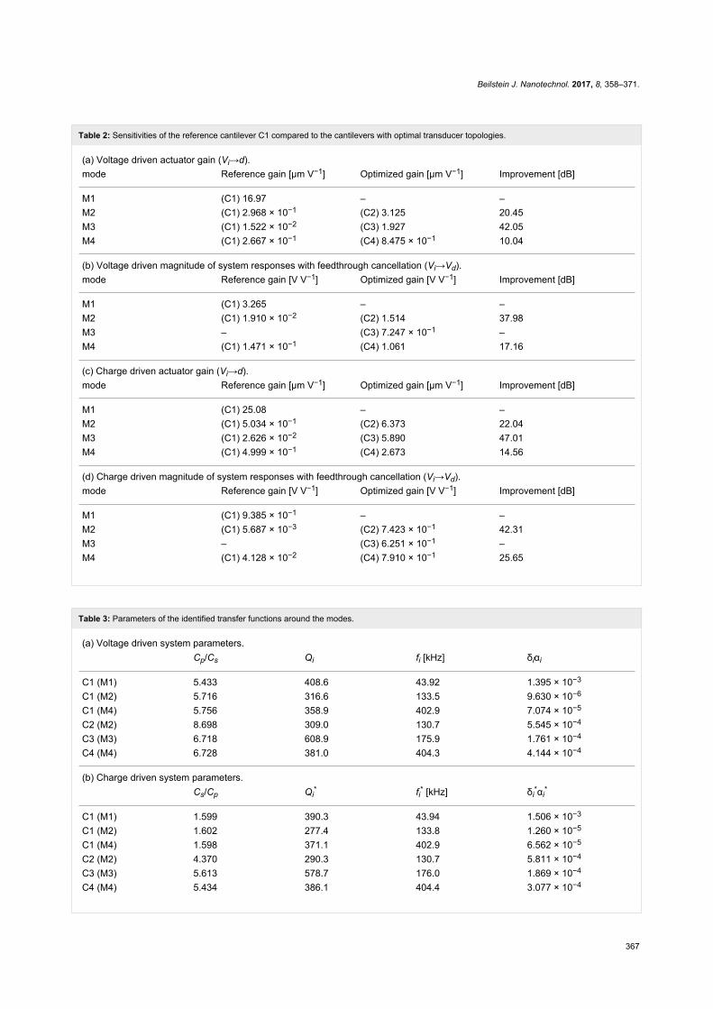
each mode is tabulated in Table 2a and c. Compared to C1 in
the voltage driven arrangement, C2 provides a 20.45 dB
increase in actuation gain for mode 2. C3 provides a 42.05 dB
increase in actuation gain for mode 3. C4 provides an 10.04 dB
increase in gain for mode 4. Compared to C1 for the charge
driven arrangement C2 provides a 22.04 dB increase in actua-
tion gain for mode 2. C3 provides a 47.01 dB increase in actua-
tion gain for mode 3. C4 provides an 14.56 dB increase in gain
for mode 4.
In Figure 6e–h and Figure 7e–h, the frequency responses from
input voltage Vi to output voltage Vo are shown. Here substan-
tial feedthrough is observed which dominates in comparison to
the motional response of the system. In a neighborhood around
the modes of interest, a third order system is identified. Transfer
functions were identified around C1 mode 2, C1 mode 4, C2
mode 2, C3 mode 3 and C4 mode 4. The motional response for
C1 mode 3 was unobservable due to the small magnitude of

Beilstein J. Nanotechnol. 2017, 8, 358–371.
366
Figure 7: Charge driven magnitude responses of the cantilevers C1–C4. (a)–(d) The responses from input voltage Vi to displacement d. The flexuralmodes of C1, C2, and C4 are measured at location 1 (L1). The torsional modes of C1 and C3 are measured at location 2 (L2) (see Figure 2m).(e)–(h) The responses from Vi to output voltage Vo. To show the resonance more clearly, the plots for C1–C4 are moved to 0 dB with a shift of−3.984 dB, −12.42 dB, −14.46 dB and −14.50 dB respectively to account for the affect of different values of Cp in each cantilever. (i)–(l) Theresponses from Vi to sensor output Vd. (b)–(d), (f)–(h) and (j)–(l) show higher resolution plots of the modes.
resonance response. The parameters of Equation 21 and Equa-
tion 23 for each of these transfer functions are tabulated in
Table 3.
The resulting magnitude responses with the feedthrough cancel-
lation from input voltage Vi to sensor output Vd, are shown in
Figure 6i–l (voltage driven) and Figure 7i–l (charge driven).
Around each mode the feedthrough is removed and the
motional component in the neighborhood of the modal frequen-
cy is revealed. The magnitudes of the motional components at
each modal frequency are tabulated in Table 2b,d. For the
voltage driven arrangement C2 increases the system response of
mode 2 by 37.98 dB. C4 increases the system response to mode
4 by 17.16 dB. For the charge driven arrangement C2 increases
the system response of mode 2 by 42.31 dB. C4 increases the
system response to mode 4 by 25.65 dB.
Noise discussionAmplitude modulation AFM always requires an actively driven
cantilever and subsequent demodulation using a lock-in ampli-
fier. Therefore, the subsequent noise characterization is for the
demodulated amplitude signal. A 4th-order low-pass filter with
cut-off frequency fc = 1 kHz is employed in the lock-in ampli-
fier (Zurich Instruments, HF2LI). The voltage noise density plot
Beilstein J. Nanotechnol. 2017, 8, 358–371.
367
Table 2: Sensitivities of the reference cantilever C1 compared to the cantilevers with optimal transducer topologies.
(a) Voltage driven actuator gain (Vi→d).mode Reference gain [μm V−1] Optimized gain [μm V−1] Improvement [dB]
M1 (C1) 16.97 – –M2 (C1) 2.968 × 10⁻¹ (C2) 3.125 20.45M3 (C1) 1.522 × 10⁻² (C3) 1.927 42.05M4 (C1) 2.667 × 10⁻¹ (C4) 8.475 × 10⁻¹ 10.04
(b) Voltage driven magnitude of system responses with feedthrough cancellation (Vi→Vd).mode Reference gain [V V−1] Optimized gain [V V−1] Improvement [dB]
M1 (C1) 3.265 – –M2 (C1) 1.910 × 10⁻² (C2) 1.514 37.98M3 – (C3) 7.247 × 10⁻¹ –M4 (C1) 1.471 × 10⁻¹ (C4) 1.061 17.16
(c) Charge driven actuator gain (Vi→d).mode Reference gain [μm V−1] Optimized gain [μm V−1] Improvement [dB]
M1 (C1) 25.08 – –M2 (C1) 5.034 × 10⁻¹ (C2) 6.373 22.04M3 (C1) 2.626 × 10⁻² (C3) 5.890 47.01M4 (C1) 4.999 × 10⁻¹ (C4) 2.673 14.56
(d) Charge driven magnitude of system responses with feedthrough cancellation (Vi→Vd).mode Reference gain [V V−1] Optimized gain [V V−1] Improvement [dB]
M1 (C1) 9.385 × 10⁻¹ – –M2 (C1) 5.687 × 10⁻³ (C2) 7.423 × 10⁻¹ 42.31M3 – (C3) 6.251 × 10⁻¹ –M4 (C1) 4.128 × 10⁻² (C4) 7.910 × 10⁻¹ 25.65
Table 3: Parameters of the identified transfer functions around the modes.
(a) Voltage driven system parameters.Cp/Cs Qi fi [kHz] δiαi
C1 (M1) 5.433 408.6 43.92 1.395 × 10⁻³
C1 (M2) 5.716 316.6 133.5 9.630 × 10⁻⁶
C1 (M4) 5.756 358.9 402.9 7.074 × 10⁻⁵
C2 (M2) 8.698 309.0 130.7 5.545 × 10⁻⁴
C3 (M3) 6.718 608.9 175.9 1.761 × 10⁻⁴
C4 (M4) 6.728 381.0 404.3 4.144 × 10⁻⁴
(b) Charge driven system parameters.Cs/Cp Qi
* fi* [kHz] δi*αi
*
C1 (M1) 1.599 390.3 43.94 1.506 × 10⁻³
C1 (M2) 1.602 277.4 133.8 1.260 × 10⁻⁵
C1 (M4) 1.598 371.1 402.9 6.562 × 10⁻⁵
C2 (M2) 4.370 290.3 130.7 5.811 × 10⁻⁴
C3 (M3) 5.613 578.7 176.0 1.869 × 10⁻⁴
C4 (M4) 5.434 386.1 404.4 3.077 × 10⁻⁴

Beilstein J. Nanotechnol. 2017, 8, 358–371.
368
Figure 8: Amplitude noise density spectra of the output voltage Vo for the reference cantilever C1 and optimized cantilevers C2–C4. (a) Voltagedriven instrumentation, (b) charge driven instrumentation.
Table 4: Sensor sensitivities and noise performance of non-optimized and optimized higher order modes.
(a) Voltage driven arrangement.C1 M1 C1 M2 C1 M4 C2 M2 C3 M3 C4 M4
Sensor sensitivity [V/μm] 0.192 0.0644 0.551 0.484 0.376 1.25RMS voltage noise [μV] 9.6959 5.4284 6.2378 7.0169 13.9297 8.2834RMS deflection noise [pm] 50.4 84.3 11.3 14.5 37.0 6.62
(b) Charge driven arrangement.C1 M1 C1 M2 C1 M4 C2 M2 C3 M3 C4 M4
Sensor sensitivity [V/μm] 0.0374 0.0113 12.11 8.586 9.422 3.379RMS voltage noise [μV] 5.7846 2.5007 2.6202 5.4924 5.3145 4.5816RMS deflection noise [pm] 154.6 221.4 31.73 47.16 50.07 15.48
of the sensor output is obtained by sampling the demodulated
amplitude at fs = 57.6 kHz and calculating a power spectral den-
sity estimate using Welch’s segment averaging estimator with
64 segments. The results are presented in Figure 8.
The RMS voltage noise present in the sensor output voltage is
obtained by integrating the noise density (Figure 8) from 0 to
fs/2. The deflection noise is obtained by dividing the voltage
noise by the identified sensor sensitivity. The sensor sensitivi-
ties are obtained by dividing the system response (Table 2b,d)
by the actuator gain (Table 2a,c) for each mode. The voltage
noise measurements are made before the feedthrough cancella-
tion, therefore the deflection noise results are for the case where
the feedthrough cancellation is noiseless. The sensor sensitivi-
ties, sensor output voltage noise and sensor output deflection
noise are tabulated in Table 4.
Due to the higher sensor sensitivities, the deflection noise has
decreased demonstrating an improved sensor performance re-
sulting from shaping the piezoelectric layer. This result occurs
when noise sources from the sensor and instrumentation domi-
nate the noise output rather than thermomechanical noise. Ther-
momechanical noise is amplified by the sensor sensitivity and
since an associated increase in noise was not observed, this
noise source must be insignificant compared to the noise from
the instrumentation.
Instrumentation for multifrequency AFMThe cantilevers fabricated and characterized in this work each
enhance the sensitivity of a single mode. To facilitate multifre-
quency AFM, it is preferable to have a cantilever optimized to
actuate and sense multiple modes and in addition allow them to
be transduced simultaneously with maximized sensitivities.
Given the linear nature of the cantilever and instrumentation,
superposition can be used to achieve this. For example, the can-
tilever C2 has the potential to optimally actuate and sense
modes M1 and M2 simultaneously. In the setup shown in
Figure 9, the M1 input voltage Vi1 is driven at the M1 reso-

Beilstein J. Nanotechnol. 2017, 8, 358–371.
369
Figure 9: To perform multifrequency AFM using cantilever C2 withmodes M1 and M2 simultaneously, the presented extension to theinstrumentation is employed.
nance frequency and is applied to both piezoelectric trans-
ducers with the same polarity to optimally actuate the cantile-
ver for M1. The outputs of the two instrumentation circuits are
combined with the same polarity to produce the optimized M1
output voltage Vo1 which maximizes the sensed response for
M1. The M2 input voltage Vi2 is combined with Vi1, however,
for the second transducer Vi2 is combined with a negative
polarity to optimally actuate M2. The optimal output voltage for
M2, Vo2, results from taking the difference between the outputs
of the two instrumentation circuits.
This principle can be extended for the design of a piezoelectric
cantilever used to actuate and sense multiple modes. The design
example for the first four modes is shown in Figure 10. By
considering the union of cantilevers C1–C4, the resulting canti-
lever has 10 separate piezoelectric transducers each with its
own instrumentation circuit. The M1–M4 input voltages
Vi1–Vi4, each driven at their respective modal resonance
frequencies, are applied to the cantilever on each transducer
with a positive polarity for black electrodes (refer to Figure 10)
and a negative polarity for white electrodes. The outputs of the
instrumentation circuits would be combined in the same fashion
for the optimized output voltages Vo1–Vo4. In comparison to
using a single piezoelectric transducer with a sum of sinusoids
excitation, the multi-electrode design provides increased ampli-
tudes at the expense of more complex instrumentation.
ConclusionAn AFM cantilever with a piezoelectric layer is a versatile
transducer for both actuation and displacement sensing. As the
response of the active layer is a function of the strain over the
surface of the cantilever, careful electrode layout has to be em-
ployed. Specifically in multifrequency AFM, the cantilever is
excited at higher order modes for which the spatial distribution
of the strain cause portions of the piezoelectric layer to contrib-
ute destructively to the transducer’s overall response. In this
Figure 10: The layout of the piezoelectric layer on the cantilever tooptimally actuate and sense M1–M4. The cantilever has 10 separatetransducers. The voltage on each transducer is a combination of fourvoltages to actuate each mode. These four voltages are combined inthe positive polarity for the black electrodes and in the negative polarityfor white electrodes. The sensor outputs for each transducer arecombined in the same fashion for each mode.
work, we have outlined a design method which provides a
systematic way of increasing the actuator gain and sensor sensi-
tivity of the self-sensing piezoelectric cantilever by considering
the spatial distribution of the strain for a given mode. The
design consists of splitting up the piezoelectric layer into
several transducers, whose individual responses are construc-
tively combined. The resulting three terminal piezoelectric
device requires additional circuitry for instrumentation com-
pared to a typical two terminal piezoelectric cantilever. For this
reason, we have proposed a grounded load charge sensor and a
grounded load charge amplifier to realize the self-sensing
implementation. The experimental results show that by shaping
the electrodes on the piezoelectric layer, significant increases in
actuator gain and sensor sensitivity are attained. Furthermore,
torsional modes are strongly observed in contrast to a cantile-
ver with an evenly distributed piezoelectric layer. Despite the
additional circuitry, no significant increase in noise was ob-
served. Future work will focus on the fabrication of cantilevers
with tips with the aim of exploiting the proposed technique to
potentially perform higher precision imaging in multifrequency
AFM.
AcknowledgementsThis work is supported by the Australian Research Council and
the University of Newcastle.
Beilstein J. Nanotechnol. 2017, 8, 358–371.
370
References1. Binnig, G.; Quate, C. F.; Gerber, C. Phys. Rev. Lett. 1986, 56,
930–933. doi:10.1103/physrevlett.56.9302. Wiesendanger, R. Scanning probe microscopy and spectroscopy;
Cambridge University Press: Cambridge, United Kingdom, 1994.3. Bhushan, B. Springer Handbook of Nanotechnology; Springer: Berlin,
Germany, 2010.4. Mazzeo, A. D.; Stein, A. J.; Trumper, D. L.; Hocken, R. J. Precis. Eng.
2009, 33, 135–149. doi:10.1016/j.precisioneng.2008.04.0075. Yamanaka, K.; Noguchi, A.; Tsuji, T.; Koike, T.; Goto, T.
Surf. Interface Anal. 1999, 27, 600–606.doi:10.1002/(sici)1096-9918(199905/06)27:5/6<600::aid-sia508>3.0.co;2-w
6. Oliver, R. A. Rep. Prog. Phys. 2008, 71, 076501.doi:10.1088/0034-4885/71/7/076501
7. Yao, T.-F.; Duenner, A.; Cullinan, M. Precis. Eng. 2017, 47, 147.doi:10.1016/j.precisioneng.2016.07.016
8. Mamin, H. J.; Rugar, D. Appl. Phys. Lett. 1992, 61, 1003–1005.doi:10.1063/1.108460
9. Minne, S. C.; Yaralioglu, G.; Manalis, S. R.; Adams, J. D.; Zesch, J.;Atalar, A.; Quate, C. F. Appl. Phys. Lett. 1998, 72, 2340–2342.doi:10.1063/1.121353
10. Vettiger, P.; Cross, G.; Despont, M.; Drechsler, U.; Durig, U.;Gotsmann, B.; Haberle, W.; Lantz, M. A.; Rothuizen, H. E.; Stutz, R.;Binnig, G. K. IEEE Trans. Nanotechnol. 2002, 99, 39–55.doi:10.1109/tnano.2002.1005425
11. Albrecht, T. R.; Akamine, S.; Carver, T. E.; Quate, C. F.J. Vac. Sci. Technol., A 1990, 8, 3386–3396. doi:10.1116/1.576520
12. Alves, M. A. R.; Takeuti, D. F.; Braga, E. S. Microelectron. J. 2005, 36,51–54. doi:10.1016/j.mejo.2004.10.004
13. Utke, I.; Hoffmann, P.; Melngailis, J.J. Vac. Sci. Technol., B: Microelectron. Nanometer Struct.–Process., Meas., Phenom. 2008, 26, 1197. doi:10.1116/1.2955728
14. García, R.; Pérez, R. Surf. Sci. Rep. 2002, 47, 197–301.doi:10.1016/S0167-5729(02)00077-8
15. Bhushan, B. Scanning Probe Microscopy in Nanoscience andNanotechnology; Springer: Berlin, Germany, 2010.
16. Garcia, R.; Herruzo, E. T. Nat. Nanotechnol. 2012, 7, 217–226.doi:10.1038/nnano.2012.38
17. Rodríguez, T. R.; García, R. Appl. Phys. Lett. 2004, 84, 449–451.doi:10.1063/1.1642273
18. Martínez, N. F.; Patil, S.; Lozano, J. R.; García, R. Appl. Phys. Lett.2006, 89, 153115. doi:10.1063/1.2360894
19. Herruzo, E. T.; Perrino, A. P.; Garcia, R. Nat. Commun. 2014, 5, 3126.doi:10.1038/ncomms4126
20. Giessibl, F. J. Mater. Today 2005, 8, 32–41.doi:10.1016/s1369-7021(05)00844-8
21. Wutscher, E.; Giessibl, F. J. Rev. Sci. Instrum. 2011, 82, 093703.doi:10.1063/1.3633950
22. Ruppert, M. G.; Moheimani, S. O. R. Beilstein J. Nanotechnol. 2016, 7,284–295. doi:10.3762/bjnano.7.26
23. Schäffer, T. E.; Cleveland, J. P.; Ohnesorge, F.; Walters, D. A.;Hansma, P. K. J. Appl. Phys. 1996, 80, 3622–3627.doi:10.1063/1.363308
24. Putman, C. A. J.; Van der Werf, K. O.; De Grooth, B. G.;Van Hulst, N. F.; Greve, J. Appl. Phys. Lett. 1994, 64, 2454–2456.doi:10.1063/1.111597
25. Han, W.; Lindsay, S. M.; Jing, T. Appl. Phys. Lett. 1996, 69,4111–4113. doi:10.1063/1.117835
26. Umeda, N.; Ishizaki, S.; Uwai, H.J. Vac. Sci. Technol., B: Microelectron. Nanometer Struct.–Process., Meas., Phenom. 1991, 9, 1318–1322. doi:10.1116/1.585187
27. Fantner, G. E.; Burns, D. J.; Belcher, A. M.; Rangelow, I. W.;Youcef-Toumi, K. J. Dyn. Syst., Meas., Control 2009, 131, 061104.doi:10.1115/1.4000378
28. Yamanaka, K.; Nakano, S. Jpn. J. Appl. Phys., Part 1 1996, 35,3787–3792. doi:10.1143/JJAP.35.3787
29. Indermühle, P.-F.; Schürmann, G.; Racine, G.-A.; de Rooij, N. F.Sens. Actuators, A 1997, 60, 186. doi:10.1016/s0924-4247(96)01440-9
30. Meyer, G.; Amer, N. M. Appl. Phys. Lett. 1988, 53, 1045–1047.doi:10.1063/1.100061
31. Kassies, R.; van der Werf, K. O.; Bennink, M. L.; Otto, C.Rev. Sci. Instrum. 2004, 75, 689–693. doi:10.1063/1.1646767
32. Eaton, P.; West, P. Atomic force microscopy; Oxford University Press:Oxford, United Kingdom, 2010.
33. Nievergelt, A. P.; Adams, J. D.; Odermatt, P. D.; Fantner, G. E.Beilstein J. Nanotechnol. 2014, 5, 2459–2467.doi:10.3762/bjnano.5.255
34. Tortonese, M.; Barrett, R. C.; Quate, C. F. Appl. Phys. Lett. 1993, 62,834–836. doi:10.1063/1.108593
35. Itoh, T.; Suga, T. Nanotechnology 1993, 4, 218–224.doi:10.1088/0957-4484/4/4/007
36. Arlett, J. L.; Maloney, J. R.; Gudlewski, B.; Muluneh, M.; Roukes, M. L.Nano Lett. 2006, 6, 1000–1006. doi:10.1021/nl060275y
37. Li, M.; Tang, H. X.; Roukes, M. L. Nat. Nanotechnol. 2007, 2, 114–120.doi:10.1038/nnano.2006.208
38. Dukic, M.; Adams, J. D.; Fantner, G. E. Sci. Rep. 2015, 5, 16393.doi:10.1038/srep16393
39. Ruppert, M. G.; Moheimani, S. O. R. Rev. Sci. Instrum. 2013, 84,125006. doi:10.1063/1.4841855
40. Ruppert, M. G.; Moheimani, S. O. R. Novel Reciprocal Self-SensingTechniques for Tapping-Mode Atomic Force Microscopy. InProceedings of 19th IFAC World Congress, IFAC World Congress,Cape Town, South Africa; 2014.
41. Sebastian, A.; Shamsudhin, N.; Rothuizen, H.; Drechsler, U.;Koelmans, W. W.; Bhaskaran, H.; Quenzer, H. J.; Wagner, B.;Despont, M. Rev. Sci. Instrum. 2012, 83, 096107.doi:10.1063/1.4755749
42. Lee, C.-K.; Moon, F. C. ASME J. Appl. Mech. 1990, 57, 434–441.doi:10.1115/1.2892008
43. Jian, K.; Friswell, M. I. J. Intell. Mater. Syst. Struct. 2007, 18, 939–948.doi:10.1177/1045389x06070589
44. Tanaka, N.; Sanada, T. Smart Mater. Struct. 2007, 16, 36–46.doi:10.1088/0964-1726/16/1/004
45. Sanchez-Rojas, J. L.; Hernando, J.; Donoso, A.; Bellido, J. C.;Manzaneque, T.; Ababneh, A.; Seidel, H.; Schmid, U.J. Micromech. Microeng. 2010, 20, 055027.doi:10.1088/0960-1317/20/5/055027
46. Donoso, A.; Bellido, J. C. Struct. Multidisc. Optim. 2009, 38, 347–356.doi:10.1007/s00158-008-0279-7
47. Sadewasser, S.; Villanueva, G.; Plaza, J. A. Appl. Phys. Lett. 2006, 89,033106. doi:10.1063/1.2226993
48. Sadewasser, S.; Villanueva, G.; Plaza, J. A. Rev. Sci. Instrum. 2006,77, 073703. doi:10.1063/1.2219738
49. Salehi-Khojin, A.; Bashash, S.; Jalili, N. J. Micromech. Microeng. 2008,18, 085008. doi:10.1088/0960-1317/18/8/085008
50. Petyt, M. Introduction to Finite Element Vibration Analysis; CambridgeUniversity Press: Cambridge, United Kingdom, 1990.

Beilstein J. Nanotechnol. 2017, 8, 358–371.
371
51. Liu, G. R.; Quek, S. S. Finite Element Method: A Practical Course;Elsevier Science: Amsterdam, Netherlands, 2003.
52. Moheimani, S. O.; Fleming, A. J. Piezoelectric Transducers forVibration Control and Damping; Springer: Berlin, Germany, 2006.
53. Jian, K.; Friswell, M. I. Mech. Syst. Signal Process. 2006, 20,2290–2304. doi:10.1016/j.ymssp.2005.05.010
54. Cowen, A.; Hames, G.; Glukh, K.; Hardy, B. PiezoMUMPs DesignHandbook, 1st ed.; MEMSCAP Inc., 2014.
55. Fleming, A. J.; Moheimani, S. O. R. IEEE Trans. Control Syst. Technol.2005, 13, 98–112. doi:10.1109/tcst.2004.838547
56. Fleming, A. J.; Moheimani, S. O. R. Rev. Sci. Instrum. 2005, 76,073707. doi:10.1063/1.1938952
57. McKelvey, T.; Akcay, H.; Ljung, L. IEEE Trans. Autom. Control 1996,41, 960–979. doi:10.1109/9.508900
License and TermsThis is an Open Access article under the terms of the
Creative Commons Attribution License
(http://creativecommons.org/licenses/by/4.0), which
permits unrestricted use, distribution, and reproduction in
any medium, provided the original work is properly cited.
The license is subject to the Beilstein Journal of
Nanotechnology terms and conditions:
(http://www.beilstein-journals.org/bjnano)
The definitive version of this article is the electronic one
which can be found at:
doi:10.3762/bjnano.8.38