mtch6102 low-power projected capacitive touch...
TRANSCRIPT

MTCH6102MTCH6102 Low-Power Projected Capacitive Touch Controller
Description:Microchip’s MTCH6102 is a turnkey projectedcapacitive touch controller that simplifies addinggestures to touch interface designs withindustry-leading low-power performance. It utilizes upto 15 channels to support taps, swipes, and scrolling onXY touch pads and touch screens. MTCH6102 allowsdesigners to quickly and easily integrate projectedcapacitive touch into their cost-sensitive, low-powerapplication. MTCH6102 provides developers with aflexible touch-sensing solution to optimize commonconstraints of size, power and cost that are critical toapplications such as wearable devices, remotecontrols, gaming devices and track pads.
Applications:• Wearable Devices such as Headphones,
Watches, Fitness Wristbands• Track Pads and Computer Peripherals• Input Devices with Configurable Button, Keypad
or Scrolling Functions• Any Interface with Single-Finger Gestures to
Swipe, Scroll, or Doubletap Controls• Home Automation Control Panels• Security Control Keypads• Automotive Center Stack Controls• Gaming Devices• Remote Control Touch Pads
Touch Sensor Support:• Up to 15 Channels• Sensor Sizes up to 120 mm (4.7”)• Individual Channel Tuning for Optimal Sensitivity• Works with Printed Circuit Board (PCB) Sensors,
Film, Glass and Flexible Printed Circuit (FPC) Sensors
Cover Layer Support:• Plastic: up to 3 mm• Glass: up to 5 mm
Touch Performance:• >200 Reports per Second (configurable)• 12-Bit Resolution Coordinate Reporting
Touch Features:• Gesture Detection and Reporting • Self-Capacitance Signal Acquisition• Multiple Built-in Filtering Options
Power Management:• Configurable Sleep/Idle Frame Rates• Standby mode <500 nA (typical) • Active mode <12 uA possible
Communication Interface:• I2C™ (up to 400 kbps)• Both Polling and Interrupt Schemes Supported• Sync Signal Allows for Host Frame Detection• Field Upgradeable over I2C
Operating Conditions:• 1.8V to 3.6V, -40°C to +85°C
Package Types:• 28-Pin SSOP• 28-Pin UQFN
2014 Microchip Technology Inc. DS40001750A-page 1
MTCH6102
Table of Contents1.0 MTCH6102 Block Diagram........................................................................................................................................................... 32.0 Pin Diagrams................................................................................................................................................................................ 43.0 MTCH6102 Pinout Description..................................................................................................................................................... 54.0 Layout........................................................................................................................................................................................... 65.0 Communication ............................................................................................................................................................................ 86.0 Sensor Design Considerations................................................................................................................................................... 107.0 Operating Modes........................................................................................................................................................................ 138.0 Controller Commands ................................................................................................................................................................ 159.0 Touch Frame Control ................................................................................................................................................................. 1610.0 Touch Data Registers................................................................................................................................................................. 1711.0 Acquisition and Touch Parameters ............................................................................................................................................ 1812.0 Compensation RAM ................................................................................................................................................................... 2013.0 Baseline...................................................................................................................................................................................... 2114.0 Gesture Features and Parameters............................................................................................................................................. 2215.0 Configuring a Non-Default Application ....................................................................................................................................... 2616.0 Manufacturing Testing................................................................................................................................................................ 2717.0 Memory Map .............................................................................................................................................................................. 2818.0 Electrical Characteristics ............................................................................................................................................................ 3119.0 Ordering Information .................................................................................................................................................................. 3520.0 Packaging Information................................................................................................................................................................ 36The Microchip Web Site........................................................................................................................................................................ 43Customer Change Notification Service................................................................................................................................................. 43Customer Support ............................................................................................................................................................................... 43Worldwide Sales and Service............................................................................................................................................................... 45TO OUR VALUED CUSTOMERSIt is our intention to provide our valued customers with the best documentation possible to ensure successful use of your Microchipproducts. To this end, we will continue to improve our publications to better suit your needs. Our publications will be refined andenhanced as new volumes and updates are introduced. If you have any questions or comments regarding this publication, please contact the Marketing Communications Department viaE-mail at [email protected]. We welcome your feedback.
Most Current Data SheetTo obtain the most up-to-date version of this data sheet, please register at our Worldwide Web site at:
http://www.microchip.comYou can determine the version of a data sheet by examining its literature number found on the bottom outside corner of any page.The last character of the literature number is the version number, (e.g., DS30000000A is version A of document DS30000000).
ErrataAn errata sheet, describing minor operational differences from the data sheet and recommended workarounds, may exist for currentdevices. As device/documentation issues become known to us, we will publish an errata sheet. The errata will specify the revisionof silicon and revision of document to which it applies.To determine if an errata sheet exists for a particular device, please check with one of the following:• Microchip’s Worldwide Web site; http://www.microchip.com• Your local Microchip sales office (see last page)When contacting a sales office, please specify which device, revision of silicon and data sheet (include literature number) you areusing.
Customer Notification SystemRegister on our web site at www.microchip.com to receive the most current information on all of our products.
DS40001750A-page 2 2014 Microchip Technology Inc.
MTCH6102
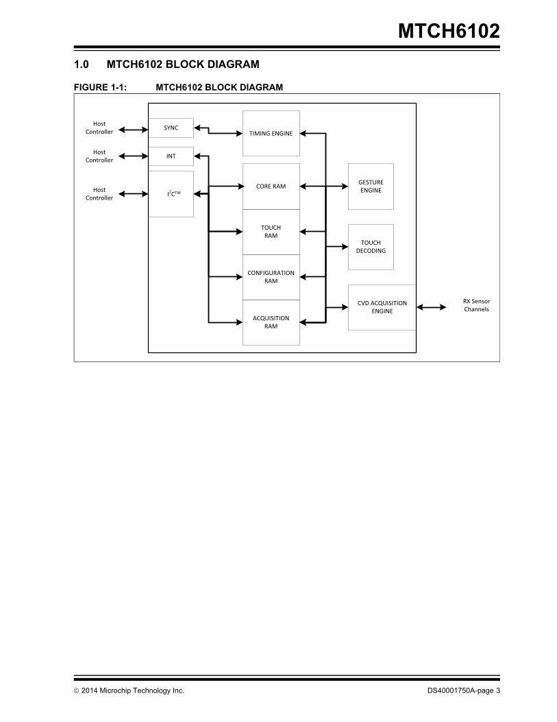
1.0 MTCH6102 BLOCK DIAGRAMFIGURE 1-1: MTCH6102 BLOCK DIAGRAM
I2C
CONFIGURATION RAM
TOUCHRAM
ACQUISITION RAM
CVD ACQUISITIONENGINE
TOUCH DECODING
GESTURE ENGINECORE RAM
TIMING ENGINE
RX Sensor Channels
Host Controller
SYNC
INTHost Controller
Host Controller
2014 Microchip Technology Inc. DS40001750A-page 3
MTCH6102
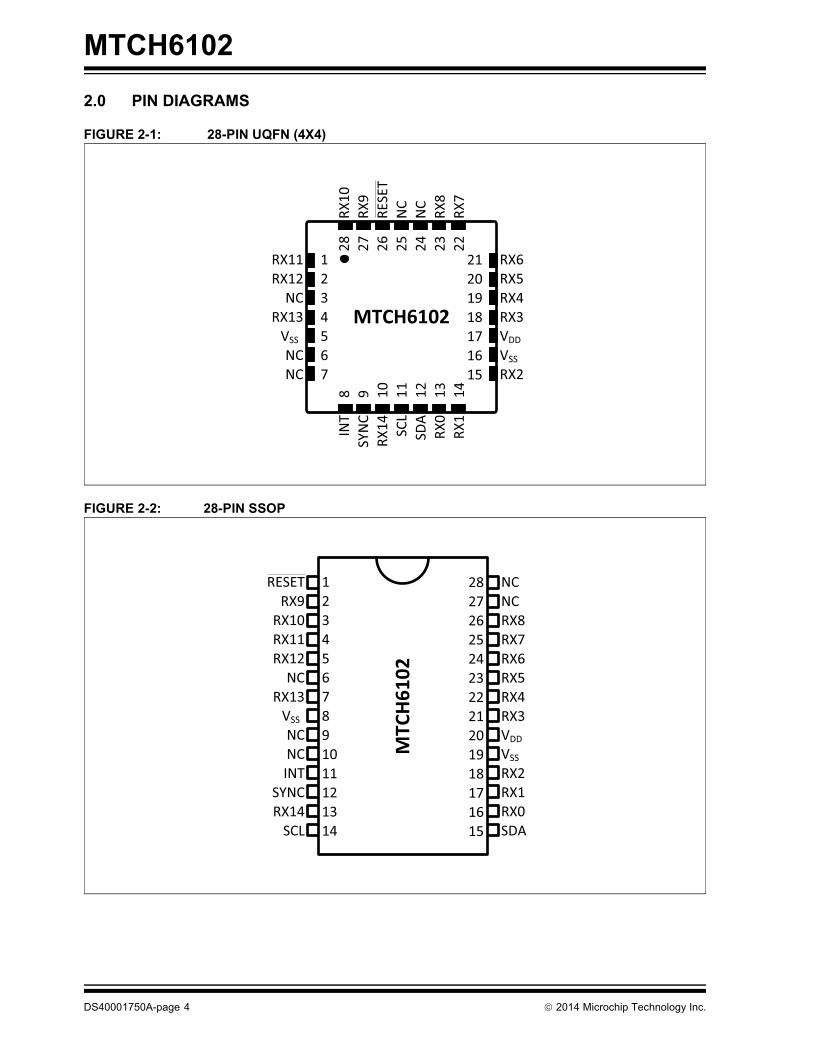
2.0 PIN DIAGRAMS
FIGURE 2-1: 28-PIN UQFN (4X4)
FIGURE 2-2: 28-PIN SSOP
MTCH6102
RX11RX12
NCRX13
VSS
NCNC
RX10
RX9
RESE
TN
CN
CRX
8RX
7
RX6RX5RX4RX3VDD
VSS
RX2
INT
SYN
CRX
14 SCL
SDA
RX0
RX1
28 27 26 25 24 23 22
8 9 10 11 12 13 14
1234567
21201918171615
MTC
H610
2
RESETRX9
RX10RX11RX12
NCRX13
VSS
NCNCINT
SYNCRX14
SCL
NCNCRX8RX7RX6RX5RX4RX3VDD
VSS
RX2RX1RX0SDA
1234567891011121314
2827262524232221201918171615
DS40001750A-page 4 2014 Microchip Technology Inc.
MTCH6102
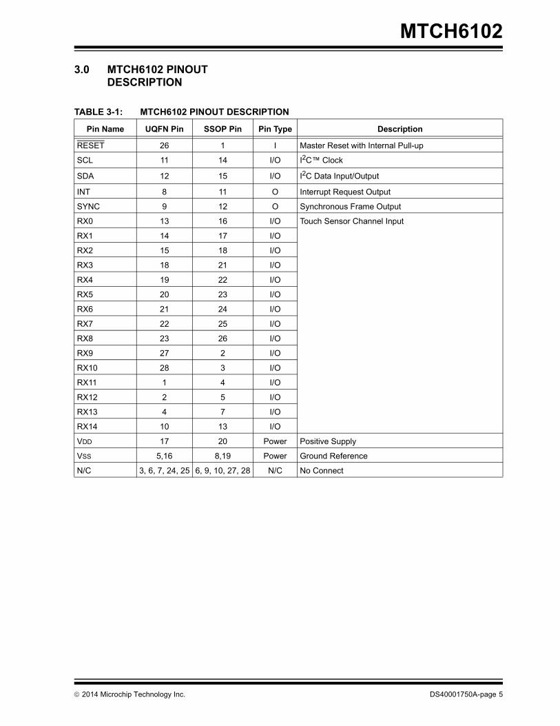
3.0 MTCH6102 PINOUT DESCRIPTION
TABLE 3-1: MTCH6102 PINOUT DESCRIPTION
Pin Name UQFN Pin SSOP Pin Pin Type Description
RESET 26 1 I Master Reset with Internal Pull-up
SCL 11 14 I/O I2C™ Clock
SDA 12 15 I/O I2C Data Input/Output
INT 8 11 O Interrupt Request Output
SYNC 9 12 O Synchronous Frame Output
RX0 13 16 I/O Touch Sensor Channel Input
RX1 14 17 I/O
RX2 15 18 I/O
RX3 18 21 I/O
RX4 19 22 I/O
RX5 20 23 I/O
RX6 21 24 I/O
RX7 22 25 I/O
RX8 23 26 I/O
RX9 27 2 I/O
RX10 28 3 I/O
RX11 1 4 I/O
RX12 2 5 I/O
RX13 4 7 I/O
RX14 10 13 I/O
VDD 17 20 Power Positive Supply
VSS 5,16 8,19 Power Ground Reference
N/C 3, 6, 7, 24, 25 6, 9, 10, 27, 28 N/C No Connect
2014 Microchip Technology Inc. DS40001750A-page 5
MTCH6102
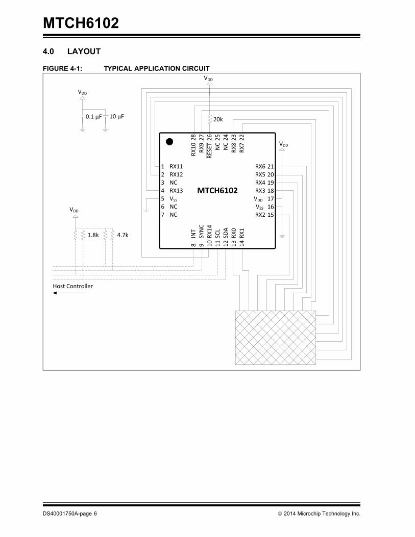
4.0 LAYOUT
FIGURE 4-1: TYPICAL APPLICATION CIRCUIT
MTCH6102
RX11RX12NCRX13VSS
NCNC
RX10 RX
9RE
SET
NC
NC
RX8
RX7
RX6RX5RX4RX3
VDD
VSS
RX2
INT
SYN
CRX
14SC
LSD
ARX
0RX
1
28 27 26 25 24 23 22
8 9 10 11 12 13 14
1234567
21201918171615
0.1 F 10 F
V
20k
4.7k1.8k
V
V
Host Controller
V
DS40001750A-page 6 2014 Microchip Technology Inc.
MTCH6102
4.1 Decoupling CapacitorsThe use of decoupling capacitors on power-supplypins, such as VDD and VSS, is required. Consider thefollowing criteria when using decoupling capacitors:1. Value and type of capacitor:
A value of 0.1 µF (100 nF), 10-20V is recommended.The capacitor should be a low Equivalent SeriesResistance (low ESR) capacitor and have resonancefrequency in the range of 20 MHz and higher. It isfurther recommended that ceramic capacitors be used.
2. Placement on the Printed Circuit Board:
The decoupling capacitors should be placed as close tothe pins as possible. It is recommended that thecapacitors be placed on the same side of the board asthe device. If space is constricted, the capacitor can beplaced on another layer on the PCB using a via;however, ensure that the trace length from the pin tothe capacitor is within one-quarter inch (6 mm) inlength.
3. Handling high-frequency noise:
If the board is experiencing high-frequency noise,upward of tens of MHz, add a second ceramic-typecapacitor in parallel to the above-described decouplingcapacitor. The value of the second capacitor can be inthe range of 0.01 µF to 0.001 µF. Place this secondcapacitor next to the primary decoupling capacitor. Inhigh-speed circuit designs, consider implementing adecade pair of capacitances as close to the power andground pins as possible (for example, 0.1 µF in parallelwith 0.001 µF).
4. Maximizing performance:
On the board layout from the power supply circuit, runthe power and return traces to the decouplingcapacitors first, and then to the device pins. Thisensures that the decoupling capacitors are first in thepower chain. It is equally important to keep the tracelength between the capacitor and the power pins to aminimum, thereby reducing PCB track inductance.
4.2 Bulk CapacitorsThe use of a bulk capacitor is recommended to improvepower-supply stability. Typical values range from4.7 µF to 47 µF. This capacitor should be located asclose to the device as possible.
2014 Microchip Technology Inc. DS40001750A-page 7
MTCH6102
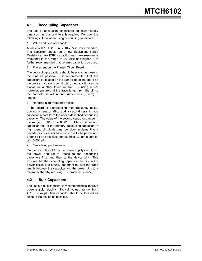
5.0 COMMUNICATION
5.1 I2C Pin Specification
5.1.1 DESCRIPTIONThe MTCH6102 low-power projected capacitive touchcontroller uses a standard register-based read/writeI2C protocol based upon the memory map. Thisprotocol is similar to many other devices such astemperature sensors and serial EEPROMs. Althoughdata can be read at any time (polling), an interrupt pin(INT) is provided for flexible integration options.
5.1.2 READING/WRITING REGISTERSTo access memory (both to read or write), the I2Ctransaction must start by addressing the chip with theWrite bit set, then writing out a single byte of datarepresenting the memory address to be operated on.After that, the host can choose to do either of thefollowing (see Figure 5-1):
1. To write memory, continue writing [n] data bytes(see Figure 5-2).
2. To read memory, restart the I2C transaction (viaeither a Stop-Start or Restart), then address thechip with the Read bit set. Continue to read in [n]data bytes (see Figure 5-3).
During either of these transactions, multiple byteswithin the same block may be read or written due to thedevice’s address auto-increment feature. SeeSection 17.0 “Memory Map” for block separation.
FIGURE 5-1: I2C™ TRANSACTION DIAGRAM
FIGURE 5-2: EXAMPLE I2C™ WRITE TRANSACTION
FIGURE 5-3: EXAMPLE I2C™ READ TRANSACTION
DATAIN DATAIN... P
SR I2CADDR R
DATAOUT ... PDATAOUT
S I2CADDR W REGADDR
Write
Read
S W
R
P I2CADDR
REGADDR
Start Condition Write Bit
Read Bit
Stop Condition
SR Restart Condition
I2CTM Device Address ( 7)
Register Address
S 0x25 W ACK 0x04 0x80 PC ACK ACK
Address Data
S 0x25 W ACK SR0x10 0x25 R ACK 0x01 NK P
INT
I C ACK
Address Data
DS40001750A-page 8 2014 Microchip Technology Inc.
MTCH6102
5.1.3 DEVICE ADDRESSINGThe MTCH6102 default 7-bit base address is 0x25.Every transmission must be prefixed with this address,as well as a bit signifying whether the transmission is amaster write (‘0’) or master read (‘1’). After appendingthis Read/Write bit to the base address, this first bytebecomes either 0x4A (write) or 0x4B (read).This address can be modified (see I2CADDR), but thisrequires initially communicating with the device underthe default address. If this is not feasible in the user’sapplication, contact Microchip support for additionaloptions.
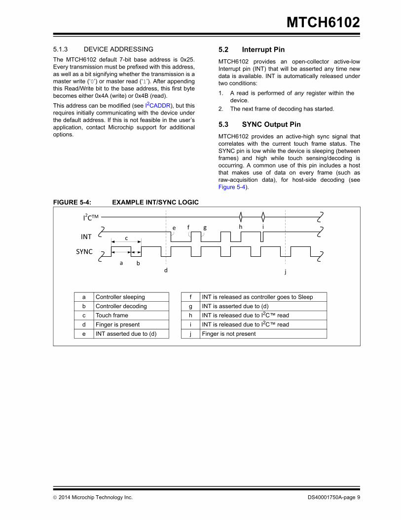
5.2 Interrupt PinMTCH6102 provides an open-collector active-lowInterrupt pin (INT) that will be asserted any time newdata is available. INT is automatically released undertwo conditions:
1. A read is performed of any register within thedevice.
2. The next frame of decoding has started.
5.3 SYNC Output PinMTCH6102 provides an active-high sync signal thatcorrelates with the current touch frame status. TheSYNC pin is low while the device is sleeping (betweenframes) and high while touch sensing/decoding isoccurring. A common use of this pin includes a hostthat makes use of data on every frame (such asraw-acquisition data), for host-side decoding (seeFigure 5-4).
FIGURE 5-4: EXAMPLE INT/SYNC LOGIC
I2C
INT
SYNCba
c
d
e f g
j
h i
a Controller sleeping f INT is released as controller goes to Sleepb Controller decoding g INT is asserted due to (d)c Touch frame h INT is released due to I2C™ readd Finger is present i INT is released due to I2C™ reade INT asserted due to (d) j Finger is not present
2014 Microchip Technology Inc. DS40001750A-page 9
MTCH6102
6.0 SENSOR DESIGN CONSIDERATIONS
6.1 General Guidelines
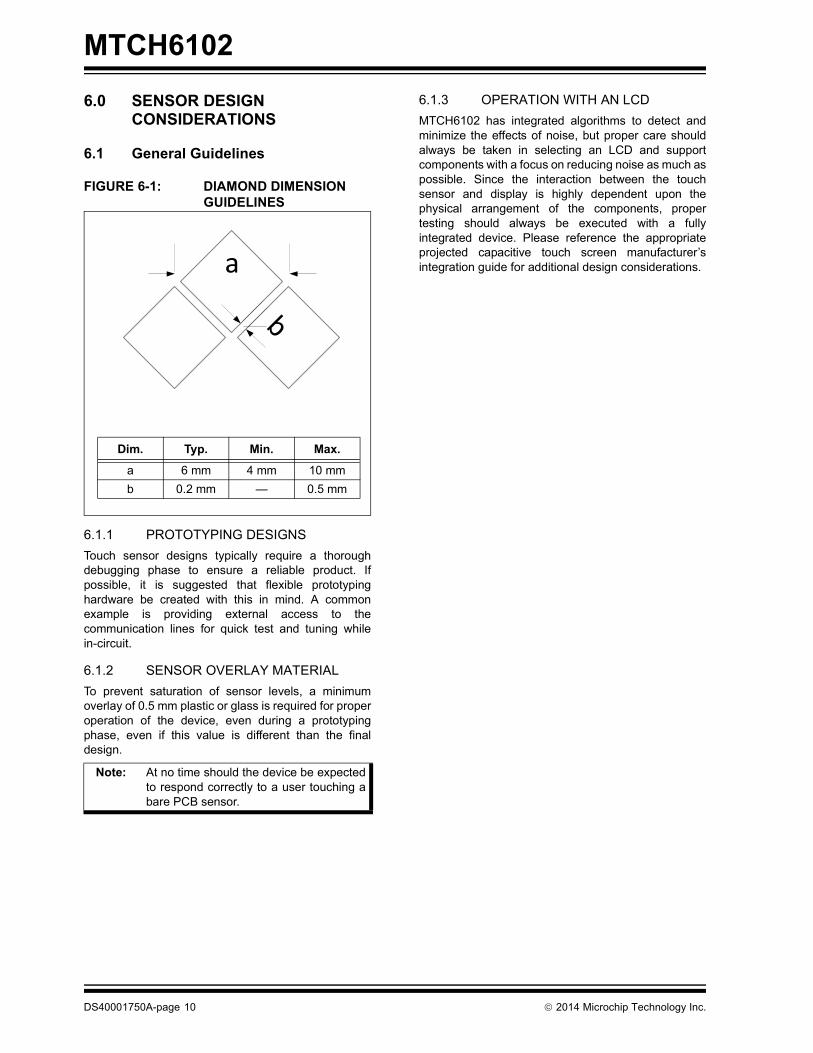
FIGURE 6-1: DIAMOND DIMENSION GUIDELINES
6.1.1 PROTOTYPING DESIGNSTouch sensor designs typically require a thoroughdebugging phase to ensure a reliable product. Ifpossible, it is suggested that flexible prototypinghardware be created with this in mind. A commonexample is providing external access to thecommunication lines for quick test and tuning whilein-circuit.
6.1.2 SENSOR OVERLAY MATERIALTo prevent saturation of sensor levels, a minimumoverlay of 0.5 mm plastic or glass is required for properoperation of the device, even during a prototypingphase, even if this value is different than the finaldesign.
6.1.3 OPERATION WITH AN LCDMTCH6102 has integrated algorithms to detect andminimize the effects of noise, but proper care shouldalways be taken in selecting an LCD and supportcomponents with a focus on reducing noise as much aspossible. Since the interaction between the touchsensor and display is highly dependent upon thephysical arrangement of the components, propertesting should always be executed with a fullyintegrated device. Please reference the appropriateprojected capacitive touch screen manufacturer’sintegration guide for additional design considerations.
Note: At no time should the device be expectedto respond correctly to a user touching abare PCB sensor.
b
a
Dim. Typ. Min. Max.
a 6 mm 4 mm 10 mmb 0.2 mm — 0.5 mm
DS40001750A-page 10 2014 Microchip Technology Inc.

MTCH6102
6.2 Sensor Layout ConfigurationMTCH6102 is designed to work with sensors with aminimum of 3x3 sensor channels, and a total maximumof 15 channels. The number of channels on each axisis governed by the registers in Table 6-1. For all sensorconfigurations, the following conditions must be met:
1. Channel layout must start at RX0.2. Each axis must have the associated channels in
either ascending or descending order.3. No unconnected channel pins are allowed in the
middle of a layout.
Table 6-2 shows an example of each rule being brokenby a 6x5 sensor layout, followed by the correct layoutin the last column.
6.3 Sensor Output ResolutionMTCH6102 interpolates 64 discrete points betweeneach channel and 32 points past the centerline of eachedge. As a result, the maximum value in the TOUCHXand TOUCHY registers will be(64xNUMBEROFCHANNELS) on each axis. For thedefault 9x6 sensor, this results in a maximum resolutionof 576x384.
TABLE 6-1: REGISTERS ASSOCIATED WITH SENSOR LAYOUT CONFIGURATIONAddress Name Description
0x20 NUMBEROFXCHANNELS Number of channels used for X axis0x21 NUMBEROFYCHANNELS Number of channels used for Y axis
TABLE 6-2: EXAMPLE OF INCORRECT 6X5 SENSOR CONNECTIONS
(1) (2) (3) Correct
RX0 X0 X0 X0
RX1 X1 X1 X1
RX2 X2 X2 X2
RX3 X4 X3 X3
RX4 X0 X3 X4 X4
RX5 X1 X5 X5 X5
RX6 X2 Y0 Y0
RX7 X3 Y2 Y1
RX8 X4 Y1 Y0 Y2
RX9 X5 Y3 Y1 Y3
RX10 Y0 Y4 Y2 Y4
RX11 Y1 Y3
RX12 Y2
RX13 Y3 Y4
RX14 Y4
2014 Microchip Technology Inc. DS40001750A-page 11
MTCH6102
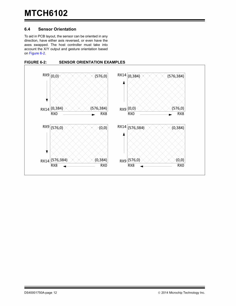
6.4 Sensor OrientationTo aid in PCB layout, the sensor can be oriented in anydirection, have either axis reversed, or even have theaxes swapped. The host controller must take intoaccount the X/Y output and gesture orientation basedon Figure 6-2.FIGURE 6-2: SENSOR ORIENTATION EXAMPLES
RX0 RX8
RX9
RX14
(0,0)
(0,384)
(576,0)
(576,384)RX0 RX8
RX14
RX9 (0,0)
(0,384)
(576,0)
(576,384)
RX8 RX0
RX9
RX14
(0,0)
(0,384)
(576,0)
(576,384)RX8 RX0
RX14
RX9 (0,0)
(0,384)
(576,0)
(576,384)
DS40001750A-page 12 2014 Microchip Technology Inc.
MTCH6102
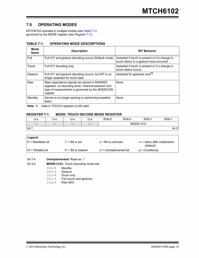
7.0 OPERATING MODESMTCH6102 operates in multiple modes (see Table 7-1)governed by the MODE register (see Register 7-1).
TABLE 7-1: OPERATING MODE DESCRIPTIONSMode Name Description INT Behavior
Full Full X/Y and gesture decoding occurs (Default mode) Asserted if touch is present or if a change in touch status or a gesture have occurred
Touch Full X/Y decoding only Asserted if touch is present or if a change in touch status occurs
Gesture Full X/Y and gesture decoding occurs, but INT is no longer asserted for touch data
Asserted for gestures only(1)
Raw Raw-capacitance signals are stored in RAWADC registers, no decoding done. Channel selection and type of measurement is governed by the MODECON register
None
Standby Device is no longer sensing or performing baseline tasks
None
Note 1: Data in TOUCH registers is still valid.
REGISTER 7-1: MODE: TOUCH DECODE MODE REGISTERU-x U-x U-x U-x R/W-0 R/W-0 R/W-1 R/W-1— — — — MODE<3:0>
bit 7 bit 0
Legend:R = Readable bit ‘1’ = Bit is set x = Bit is unknown -n = Value after initialization
(default)W = Writable bit ‘0’ = Bit is cleared U = Unimplemented bit q = Conditional
bit 7-4 Unimplemented: Read as ‘0’ bit 3-0 MODE<3:0>: Touch Decoding mode bits
0000 = Standby0001 = Gesture0010 = Touch only0011 = Full (touch and gesture)01XX = Raw ADC
2014 Microchip Technology Inc. DS40001750A-page 13
MTCH6102
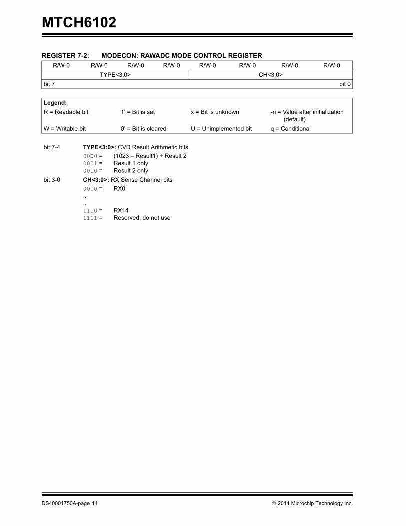
REGISTER 7-2: MODECON: RAWADC MODE CONTROL REGISTERR/W-0 R/W-0 R/W-0 R/W-0 R/W-0 R/W-0 R/W-0 R/W-0
TYPE<3:0> CH<3:0>bit 7 bit 0
Legend:R = Readable bit ‘1’ = Bit is set x = Bit is unknown -n = Value after initialization
(default)W = Writable bit ‘0’ = Bit is cleared U = Unimplemented bit q = Conditional
bit 7-4 TYPE<3:0>: CVD Result Arithmetic bits0000 = (1023 – Result1) + Result 20001 = Result 1 only0010 = Result 2 only
bit 3-0 CH<3:0>: RX Sense Channel bits0000 = RX0....1110 = RX141111 = Reserved, do not use
DS40001750A-page 14 2014 Microchip Technology Inc.
MTCH6102
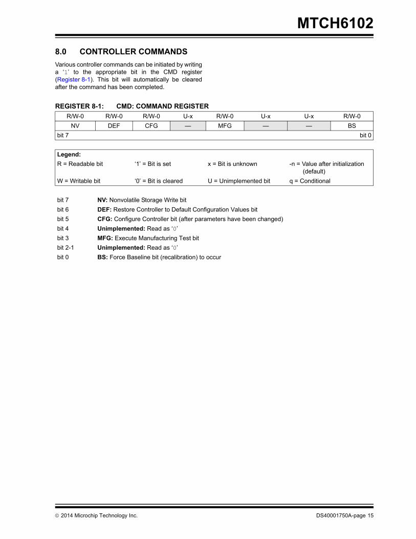
8.0 CONTROLLER COMMANDSVarious controller commands can be initiated by writinga ‘1’ to the appropriate bit in the CMD register(Register 8-1). This bit will automatically be clearedafter the command has been completed.
REGISTER 8-1: CMD: COMMAND REGISTERR/W-0 R/W-0 R/W-0 U-x R/W-0 U-x U-x R/W-0
NV DEF CFG — MFG — — BSbit 7 bit 0
Legend:R = Readable bit ‘1’ = Bit is set x = Bit is unknown -n = Value after initialization
(default)W = Writable bit ‘0’ = Bit is cleared U = Unimplemented bit q = Conditional
bit 7 NV: Nonvolatile Storage Write bitbit 6 DEF: Restore Controller to Default Configuration Values bitbit 5 CFG: Configure Controller bit (after parameters have been changed)bit 4 Unimplemented: Read as ‘0’bit 3 MFG: Execute Manufacturing Test bitbit 2-1 Unimplemented: Read as ‘0’bit 0 BS: Force Baseline bit (recalibration) to occur
2014 Microchip Technology Inc. DS40001750A-page 15
MTCH6102
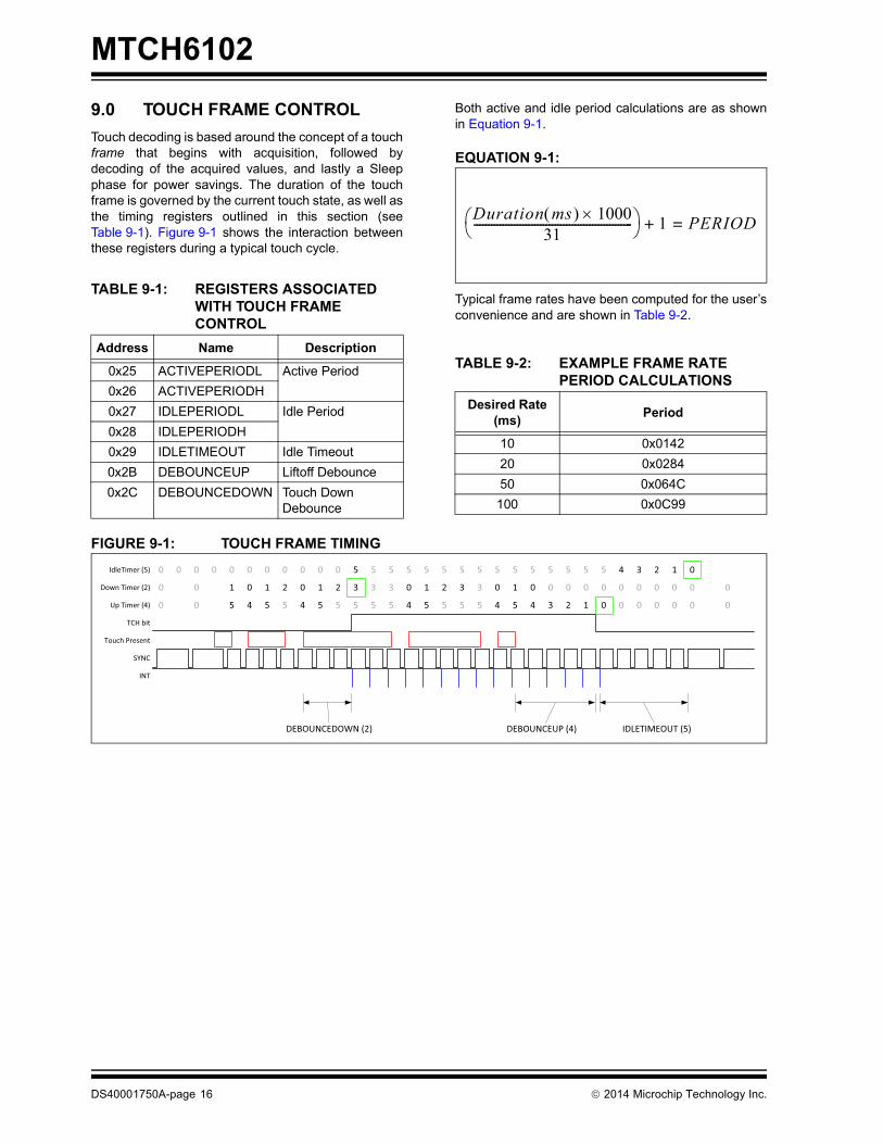
9.0 TOUCH FRAME CONTROLTouch decoding is based around the concept of a touchframe that begins with acquisition, followed bydecoding of the acquired values, and lastly a Sleepphase for power savings. The duration of the touchframe is governed by the current touch state, as well asthe timing registers outlined in this section (seeTable 9-1). Figure 9-1 shows the interaction betweenthese registers during a typical touch cycle.
Both active and idle period calculations are as shownin Equation 9-1.
EQUATION 9-1:
Typical frame rates have been computed for the user’sconvenience and are shown in Table 9-2.
FIGURE 9-1: TOUCH FRAME TIMING
TABLE 9-1: REGISTERS ASSOCIATED WITH TOUCH FRAME CONTROL
Address Name Description
0x25 ACTIVEPERIODL Active Period0x26 ACTIVEPERIODH0x27 IDLEPERIODL Idle Period0x28 IDLEPERIODH0x29 IDLETIMEOUT Idle Timeout0x2B DEBOUNCEUP Liftoff Debounce0x2C DEBOUNCEDOWN Touch Down
Debounce
TABLE 9-2: EXAMPLE FRAME RATE PERIOD CALCULATIONS
Desired Rate (ms) Period
10 0x014220 0x028450 0x064C
100 0x0C99
Duration ms 100031-------------------------------------------------------
1 PERIOD=+
Touch Present
SYNC
Up Timer (4)
Down Timer (2)
IdleTimer (5)
TCH bit
0 5
0 1 0 1 2 0 1 2 3 3 3 0 1 2 3 3 0 1 0 0 0 0 0
4 5 5 4 5 5 5 5 5 4 5 5 5 5 4 5 4 3 2 1 00
0
0 0 0 0 0 0 0 0 0 0 0 5 5 5 5 5 5 5 5 4 3 2
0
0
0
0
0
0
0
0
0
0
0
0
1 05 5 5 5 5 5 5
INT
IDLETIMEOUT (5)DEBOUNCEUP (4)DEBOUNCEDOWN (2)
DS40001750A-page 16 2014 Microchip Technology Inc.
MTCH6102
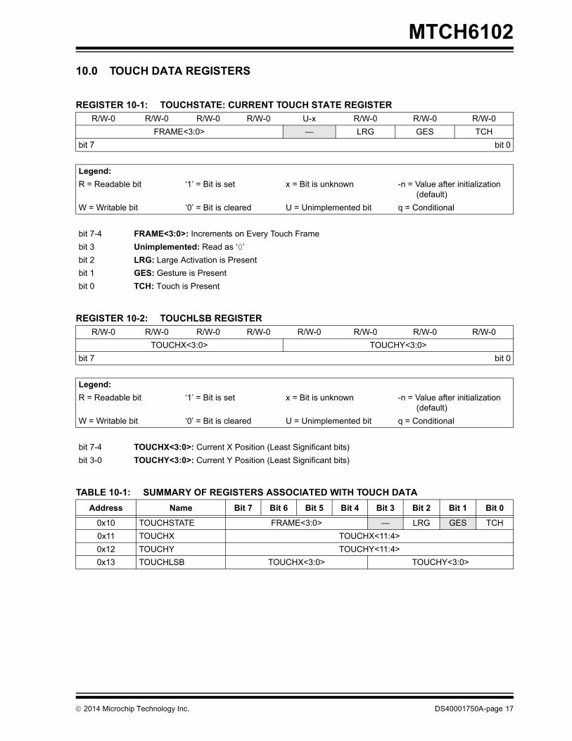
10.0 TOUCH DATA REGISTERS
REGISTER 10-1: TOUCHSTATE: CURRENT TOUCH STATE REGISTERR/W-0 R/W-0 R/W-0 R/W-0 U-x R/W-0 R/W-0 R/W-0
FRAME<3:0> — LRG GES TCHbit 7 bit 0
Legend:R = Readable bit ‘1’ = Bit is set x = Bit is unknown -n = Value after initialization
(default)W = Writable bit ‘0’ = Bit is cleared U = Unimplemented bit q = Conditional
bit 7-4 FRAME<3:0>: Increments on Every Touch Framebit 3 Unimplemented: Read as ‘0’bit 2 LRG: Large Activation is Presentbit 1 GES: Gesture is Presentbit 0 TCH: Touch is Present
REGISTER 10-2: TOUCHLSB REGISTERR/W-0 R/W-0 R/W-0 R/W-0 R/W-0 R/W-0 R/W-0 R/W-0
TOUCHX<3:0> TOUCHY<3:0>bit 7 bit 0
Legend:R = Readable bit ‘1’ = Bit is set x = Bit is unknown -n = Value after initialization
(default)W = Writable bit ‘0’ = Bit is cleared U = Unimplemented bit q = Conditional
bit 7-4 TOUCHX<3:0>: Current X Position (Least Significant bits)bit 3-0 TOUCHY<3:0>: Current Y Position (Least Significant bits)
TABLE 10-1: SUMMARY OF REGISTERS ASSOCIATED WITH TOUCH DATAAddress Name Bit 7 Bit 6 Bit 5 Bit 4 Bit 3 Bit 2 Bit 1 Bit 0
0x10 TOUCHSTATE FRAME<3:0> — LRG GES TCH0x11 TOUCHX TOUCHX<11:4>0x12 TOUCHY TOUCHY<11:4>0x13 TOUCHLSB TOUCHX<3:0> TOUCHY<3:0>
2014 Microchip Technology Inc. DS40001750A-page 17
MTCH6102
11.0 ACQUISITION AND TOUCH PARAMETERS
11.1 SCANCOUNTEvery time a channel is scanned, it is scanned multipletimes (SCANCOUNT) and summed. Increasing thisnumber will give an inherent averaging effect, but at thecost of time and subsequently increased powerconsumption.
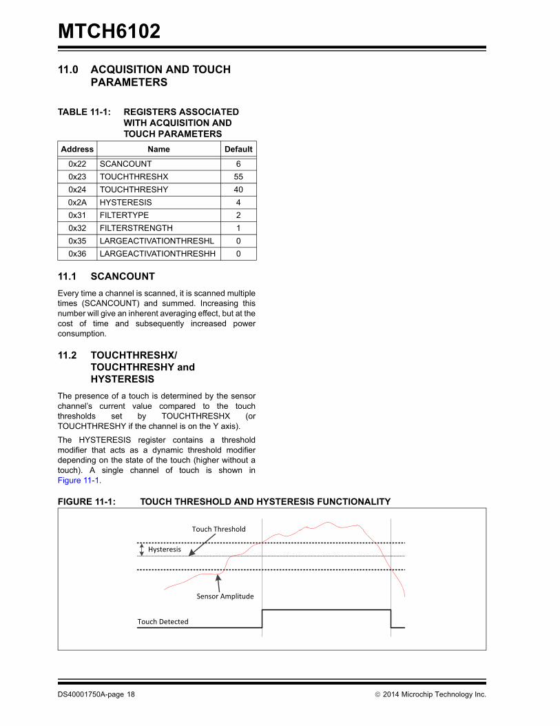
11.2 TOUCHTHRESHX/ TOUCHTHRESHY and HYSTERESIS
The presence of a touch is determined by the sensorchannel’s current value compared to the touchthresholds set by TOUCHTHRESHX (orTOUCHTHRESHY if the channel is on the Y axis).
The HYSTERESIS register contains a thresholdmodifier that acts as a dynamic threshold modifierdepending on the state of the touch (higher without atouch). A single channel of touch is shown inFigure 11-1.
FIGURE 11-1: TOUCH THRESHOLD AND HYSTERESIS FUNCTIONALITY
TABLE 11-1: REGISTERS ASSOCIATED WITH ACQUISITION AND TOUCH PARAMETERS
Address Name Default
0x22 SCANCOUNT 60x23 TOUCHTHRESHX 550x24 TOUCHTHRESHY 400x2A HYSTERESIS 40x31 FILTERTYPE 20x32 FILTERSTRENGTH 10x35 LARGEACTIVATIONTHRESHL 00x36 LARGEACTIVATIONTHRESHH 0
Hysteresis
Touch Threshold
Sensor Amplitude
Touch Detected
DS40001750A-page 18 2014 Microchip Technology Inc.
MTCH6102
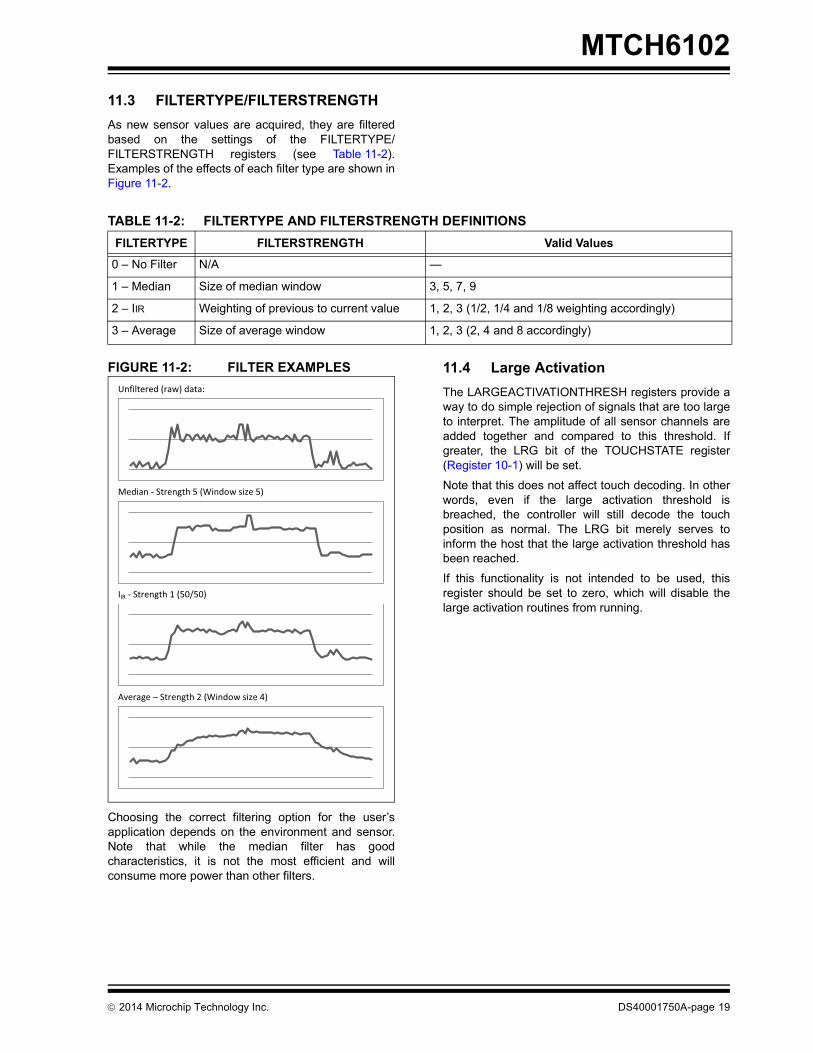
11.3 FILTERTYPE/FILTERSTRENGTHAs new sensor values are acquired, they are filteredbased on the settings of the FILTERTYPE/FILTERSTRENGTH registers (see Table 11-2).Examples of the effects of each filter type are shown inFigure 11-2.FIGURE 11-2: FILTER EXAMPLES
Choosing the correct filtering option for the user’sapplication depends on the environment and sensor.Note that while the median filter has goodcharacteristics, it is not the most efficient and willconsume more power than other filters.
11.4 Large ActivationThe LARGEACTIVATIONTHRESH registers provide away to do simple rejection of signals that are too largeto interpret. The amplitude of all sensor channels areadded together and compared to this threshold. Ifgreater, the LRG bit of the TOUCHSTATE register(Register 10-1) will be set.
Note that this does not affect touch decoding. In otherwords, even if the large activation threshold isbreached, the controller will still decode the touchposition as normal. The LRG bit merely serves toinform the host that the large activation threshold hasbeen reached.
If this functionality is not intended to be used, thisregister should be set to zero, which will disable thelarge activation routines from running.
TABLE 11-2: FILTERTYPE AND FILTERSTRENGTH DEFINITIONSFILTERTYPE FILTERSTRENGTH Valid Values
0 – No Filter N/A —
1 – Median Size of median window 3, 5, 7, 9
2 – IIR Weighting of previous to current value 1, 2, 3 (1/2, 1/4 and 1/8 weighting accordingly)
3 – Average Size of average window 1, 2, 3 (2, 4 and 8 accordingly)
Unfiltered (raw) data:
Median - Strength 5 (Window size 5)
IIR - Strength 1 (50/50)
Average – Strength 2 (Window size 4)
2014 Microchip Technology Inc. DS40001750A-page 19
MTCH6102
12.0 COMPENSATION RAMIt is very common for a typical touch sensor to havenon-uniform capacitive properties. To equalize thesensor, a series of coefficients can be written to thecompensation RAM block. These coefficientsrepresent a ratio that is applied to the individualchannel in post-acquisition, before touch decodingoccurs.
EQUATION 12-1: COMPENSATION RAM CALCULATION
To obtain the correct compensation RAM values, thefollowing procedure should be used:
1. Set all SENSORVALUES registers to zero (ifnecessary).
2. Record the peak values that occur in theSENSORVALUES registers when using thesensor under normal conditions (column A ofTable 12-1).
3. Pick a commonly occurring value to representthe median of the set (‘125’).
4. Calculate the ratio of the peak value by dividingthe median value by the peak (column B).
5. Multiply this value by 64 and truncate (columnC). These are the compensation values thatshould be written to the SENSORCOMPregisters. Please note that, if no compensationis required (value of ‘64’, ratio of ‘1’), the registershould be set to ‘0’, to save time runningcompensation routines for that channel.
6. To see the expected output from thecompensation values, follow Equation 12-1(result in column D).
RAW VALUE SENSORCOMP64
---------------------------------------------------------------------------------------- FINAL VALUE =
TABLE 12-1: COMPENSATION RAM EXAMPLE CALCULATION
CH A B C D
0 102 1.225 78 124
1 113 1.106 71 125
2 118 1.059 68 125
3 125 1 64 (0) 125
4 125 1 64 (0) 125
5 128 0.977 63 126
6 132 0.947 61 126
7 160 0.781 50 125
DS40001750A-page 20 2014 Microchip Technology Inc.
MTCH6102
13.0 BASELINECapacitive touch principles rely on analyzing a changein capacitance from a previously-stored baseline value(sometimes referred to as a calibration value). Baselineroutines and behavior can be tweaked using theregisters listed in Table 13-1.
13.1 BS Bit (CMD Register)The BS bit forces the current sensor values to bestored as the baseline values, disregarding theconstraints of BASEPOSFILTER andBASENEGFILTER.
13.2 BASEINTERVALIt represents the number of touch frames betweenbaseline sampling. Data that is sampled will be appliedat the next baseline interval, provided that a touch hasnot occurred between the two.
If at any point, the touch threshold is breached, thebaseline counter is reset, and a full interval without atouch must occur before baselining resumes.
Note that this value is specified in terms of the numberof touch frames, so any changes in frame rate shouldtake this into consideration by raising or lowering thisinterval accordingly.
13.3 BASEPOSFILTER/BASENEGFILTERThe positive and negative filters act as slew-ratelimiters for a new baseline being applied. For example,if the new baseline value is larger than the previous bya value of 35, and the BASEPOSFILTER is set to 20(default), the new baseline will only be increased by 20.
Use of these registers helps prevent unwanted spikesin the baseline value.
13.4 BASEFILTERTYPE/ BASEFILTERSTRENGTH
Baseline acquisition frames follow the same filter typeand strength parameters as normal acquisition filters,defined in Section 11.3 “FILTERTYPE/FILTER-STRENGTH”.
TABLE 13-1: REGISTERS ASSOCIATED WITH BASELINEAddress Bit 7 Bit 6 Bit 5 Bit 4 Bit 3 Bit 2 Bit 1 Bit 0 Default
0x04 NV DEF CFG - MFG - - BS 0
0x2D BASEINTERVALL 10
0x2E BASEINTERVALH 0
0x2F BASEPOSFILTER 20
0x30 BASENEGFILTER 20
0x33 BASEFILTERTYPE 2
0x34 BASEFILTERSTRENGTH 1
2014 Microchip Technology Inc. DS40001750A-page 21
MTCH6102
14.0 GESTURE FEATURES AND PARAMETERS
Gesture detection and reporting is governed by theregisters outlined in Table 14-1.
When a gesture is performed, the gesture ID will beplaced in GESTURESTATE, and the GES bit of theTOUCHSTATE register will be set. Both of these itemsare cleared after reading the GESTURESTATEregister. The GESTUREDIAG register contains a codeexplaining the logic behind the last operation of thegesture engine, primarily to help with debugging of thegesture parameters. These diagnostic codes areshown in Register 14-2.
TABLE 14-1: SUMMARY OF REGISTERS ASSOCIATED WITH GESTURESAddress Name Bit 7 Bit 6 Bit 5 Bit 4 Bit 3 Bit 2 Bit 1 Bit 0 Default
0x10 TOUCHSTATE FRAME<3:0> - LRG GES TCH N/A
0x14 GESTURESTATE GESTURESTATE 0
0x15 GESTUREDIAG GESTUREDIAG 0
0x37 HORIZONTALSWIPEDISTANCE HORIZONTALSWIPEDISTANCE 64
0x38 VERTICALSWIPEDISTANCE VERTICALSWIPEDISTANCE 64
0x39 SWIPEHOLDBOUNDARY SWIPEHOLDBOUNDARY 25
0x3A TAPDISTANCE TAPDISTANCE 25
0x3B DISTANCEBETWEENTAPS DISTANCEBETWEENTAPS 64
0x3CTAPHOLDTIME
TAPHOLDTIMEL 50
0x3D TAPHOLDTIMEH 0
0x3E GESTURECLICKTIME GESTURECLICKTIME 12
0x3F SWIPEHOLDTHRESH SWIPEHOLDTHRESH 32
0x40 MINSWIPEVELOCITY MINSWIPEVELOCITY 4
0x41 HORIZONTALGESTUREANGLE HORIZONTALGESTUREANGLE 45
0x42 VERTICALGESTUREANGLE VERTICALGESTUREANGLE 45
DS40001750A-page 22 2014 Microchip Technology Inc.
MTCH6102
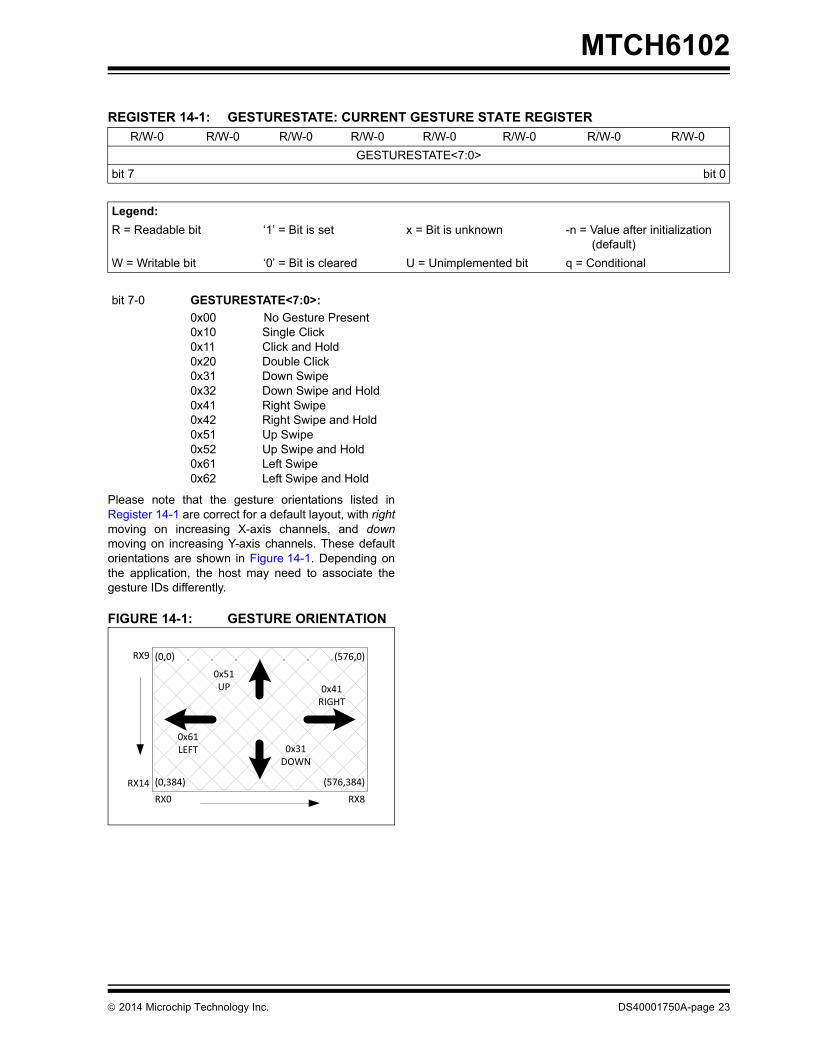
Please note that the gesture orientations listed inRegister 14-1 are correct for a default layout, with rightmoving on increasing X-axis channels, and downmoving on increasing Y-axis channels. These defaultorientations are shown in Figure 14-1. Depending onthe application, the host may need to associate thegesture IDs differently.
FIGURE 14-1: GESTURE ORIENTATION
REGISTER 14-1: GESTURESTATE: CURRENT GESTURE STATE REGISTERR/W-0 R/W-0 R/W-0 R/W-0 R/W-0 R/W-0 R/W-0 R/W-0
GESTURESTATE<7:0>bit 7 bit 0
Legend:R = Readable bit ‘1’ = Bit is set x = Bit is unknown -n = Value after initialization
(default)W = Writable bit ‘0’ = Bit is cleared U = Unimplemented bit q = Conditional
bit 7-0 GESTURESTATE<7:0>:0x00 No Gesture Present0x10 Single Click0x11 Click and Hold0x20 Double Click0x31 Down Swipe0x32 Down Swipe and Hold0x41 Right Swipe0x42 Right Swipe and Hold0x51 Up Swipe0x52 Up Swipe and Hold0x61 Left Swipe0x62 Left Swipe and Hold
RX0 RX8
RX9
RX14 (0,384)
(0,0)
(576,384)
(576,0)
0x41RIGHT
0x61LEFT
0x51UP
0x31DOWN
2014 Microchip Technology Inc. DS40001750A-page 23
MTCH6102
REGISTER 14-2: GESTUREDIAG: GESTURE DIAGNOSTICS REGISTERR/W-0 R/W-0 R/W-0 R/W-0 R/W-0 R/W-0 R/W-0 R/W-0
GESTUREDIAG<7:0>bit 7 bit 0
Legend:R = Readable bit ‘1’ = Bit is set x = Bit is unknown -n = Value after initialization
(default)W = Writable bit ‘0’ = Bit is cleared U = Unimplemented bit q = Conditional
bit 7-0 GESTUREDIAG<7:0>:0x01 Click Timeout0x02 Swipe Timeout0x03 General Timeout0x04 Click Threshold Exceeded0x05 Swipe Threshold Exceeded0x06 Swipe and Hold Threshold Exceeded0x07 Swipe Opposite Direction Threshold Exceeded0x08 Reserved0x09 Swipe and Hold Value Exceeded0x0A Outside Swipe Angle
DS40001750A-page 24 2014 Microchip Technology Inc.
MTCH6102
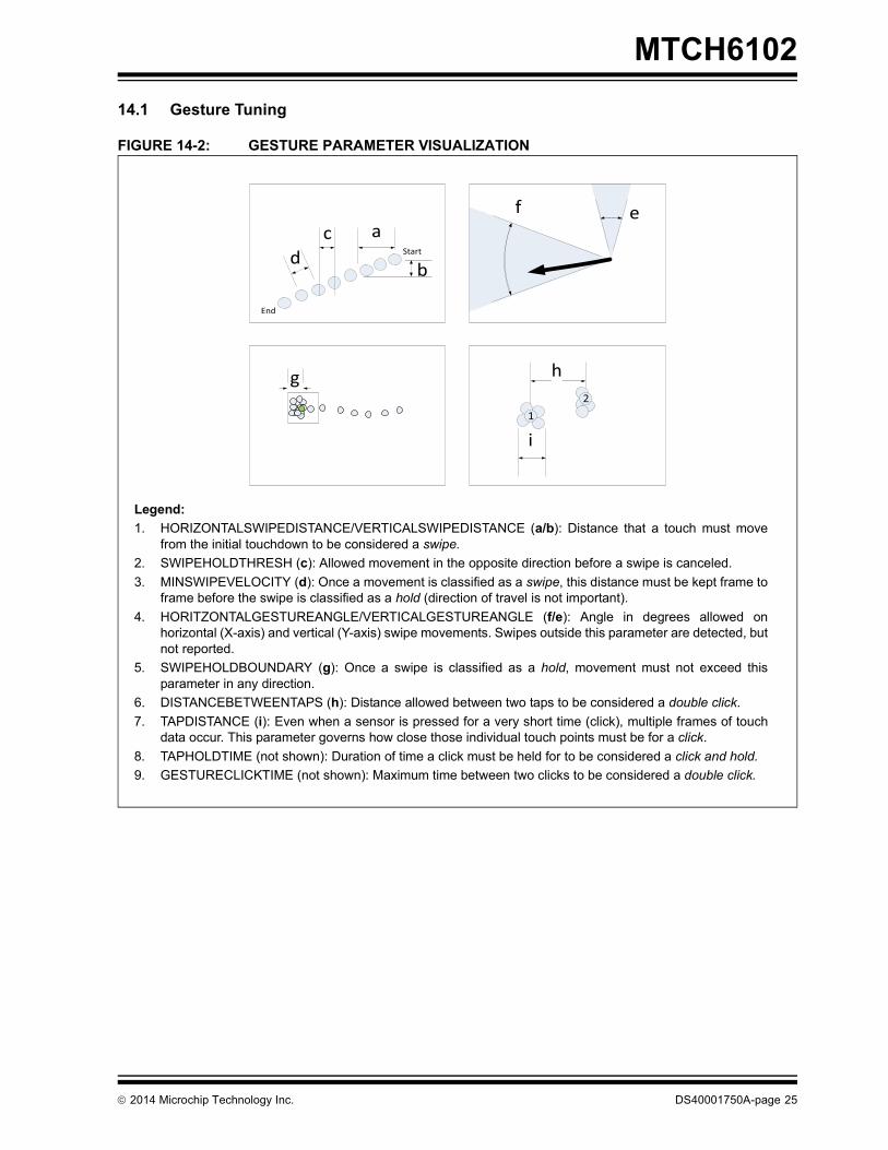
14.1 Gesture TuningFIGURE 14-2: GESTURE PARAMETER VISUALIZATION
af e
bStart
End
g
dc
h
12
i
Legend:1. HORIZONTALSWIPEDISTANCE/VERTICALSWIPEDISTANCE (a/b): Distance that a touch must move
from the initial touchdown to be considered a swipe.2. SWIPEHOLDTHRESH (c): Allowed movement in the opposite direction before a swipe is canceled.3. MINSWIPEVELOCITY (d): Once a movement is classified as a swipe, this distance must be kept frame to
frame before the swipe is classified as a hold (direction of travel is not important).4. HORITZONTALGESTUREANGLE/VERTICALGESTUREANGLE (f/e): Angle in degrees allowed on
horizontal (X-axis) and vertical (Y-axis) swipe movements. Swipes outside this parameter are detected, butnot reported.
5. SWIPEHOLDBOUNDARY (g): Once a swipe is classified as a hold, movement must not exceed thisparameter in any direction.
6. DISTANCEBETWEENTAPS (h): Distance allowed between two taps to be considered a double click.7. TAPDISTANCE (i): Even when a sensor is pressed for a very short time (click), multiple frames of touch
data occur. This parameter governs how close those individual touch points must be for a click.8. TAPHOLDTIME (not shown): Duration of time a click must be held for to be considered a click and hold.9. GESTURECLICKTIME (not shown): Maximum time between two clicks to be considered a double click.
2014 Microchip Technology Inc. DS40001750A-page 25
MTCH6102
15.0 CONFIGURING A NON-DEFAULT APPLICATION
When modifying sensor configuration parameters, theCFG bit of the CMD register must be set for theconfiguration to take effect. Setting this bit analyzes thefollowing registers for validity and coerces them ifnecessary:
1. IDLEPERIOD/ACTIVEPERIOD2. FILTERTYPE/FILTERSTRENGTH3. BASELINEFILTERTYPE/FILTERSTRENGTH4. NUMBEROFXCHANNELS/NUMBEROFYCHAN-
NELS
Afterwards, the values take effect, and the sensor isbase-lined and ready for use.
Most applications will require custom parameters to bestored in the configuration RAM. The followingmethods are recommended for achieving this:
1. For permanent configuration: Either duringmanufacturing test or on first start-up, the hostcontroller writes all configuration values to thecontroller, sets the CFG bit and stores them toNVRAM by using the NV bit.
2. For configuration on every power-up: The hostwrites all configuration data to the controller andsets the CFG bit on start-up.
Note: If the controller is not in Standby modewhen changing configuration parameters,unreliable touch data may be generateduntil the CFG is set.
DS40001750A-page 26 2014 Microchip Technology Inc.
MTCH6102
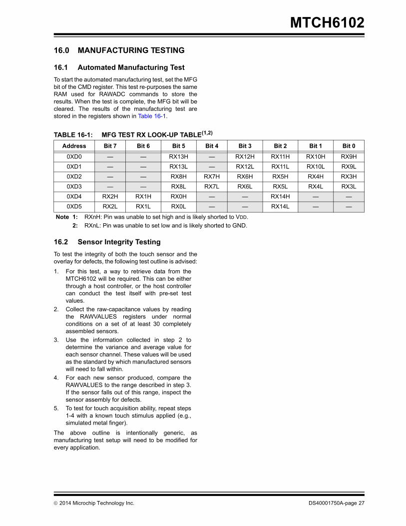
16.0 MANUFACTURING TESTING
16.1 Automated Manufacturing TestTo start the automated manufacturing test, set the MFGbit of the CMD register. This test re-purposes the sameRAM used for RAWADC commands to store theresults. When the test is complete, the MFG bit will becleared. The results of the manufacturing test arestored in the registers shown in Table 16-1.
16.2 Sensor Integrity TestingTo test the integrity of both the touch sensor and theoverlay for defects, the following test outline is advised:
1. For this test, a way to retrieve data from theMTCH6102 will be required. This can be eitherthrough a host controller, or the host controllercan conduct the test itself with pre-set testvalues.
2. Collect the raw-capacitance values by readingthe RAWVALUES registers under normalconditions on a set of at least 30 completelyassembled sensors.
3. Use the information collected in step 2 todetermine the variance and average value foreach sensor channel. These values will be usedas the standard by which manufactured sensorswill need to fall within.
4. For each new sensor produced, compare theRAWVALUES to the range described in step 3.If the sensor falls out of this range, inspect thesensor assembly for defects.
5. To test for touch acquisition ability, repeat steps1-4 with a known touch stimulus applied (e.g.,simulated metal finger).
The above outline is intentionally generic, asmanufacturing test setup will need to be modified forevery application.
TABLE 16-1: MFG TEST RX LOOK-UP TABLE(1,2)
Address Bit 7 Bit 6 Bit 5 Bit 4 Bit 3 Bit 2 Bit 1 Bit 0
0XD0 — — RX13H — RX12H RX11H RX10H RX9H
0XD1 — — RX13L — RX12L RX11L RX10L RX9L
0XD2 — — RX8H RX7H RX6H RX5H RX4H RX3H
0XD3 — — RX8L RX7L RX6L RX5L RX4L RX3L
0XD4 RX2H RX1H RX0H — — RX14H — —
0XD5 RX2L RX1L RX0L — — RX14L — —
Note 1: RXnH: Pin was unable to set high and is likely shorted to VDD.2: RXnL: Pin was unable to set low and is likely shorted to GND.
2014 Microchip Technology Inc. DS40001750A-page 27
MTCH6102
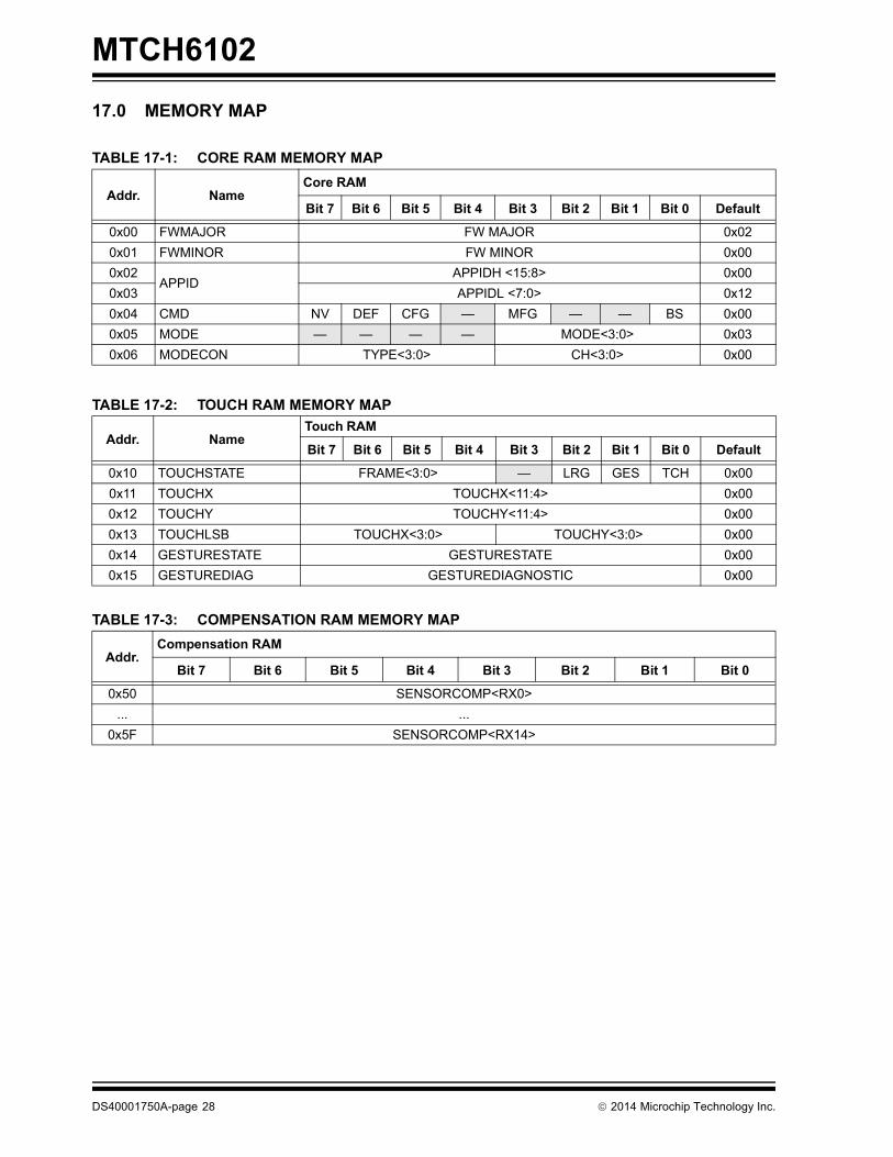
17.0 MEMORY MAP
TABLE 17-1: CORE RAM MEMORY MAP
Addr. NameCore RAM
Bit 7 Bit 6 Bit 5 Bit 4 Bit 3 Bit 2 Bit 1 Bit 0 Default
0x00 FWMAJOR FW MAJOR 0x020x01 FWMINOR FW MINOR 0x000x02
APPIDAPPIDH <15:8> 0x00
0x03 APPIDL <7:0> 0x120x04 CMD NV DEF CFG — MFG — — BS 0x000x05 MODE — — — — MODE<3:0> 0x030x06 MODECON TYPE<3:0> CH<3:0> 0x00
TABLE 17-2: TOUCH RAM MEMORY MAP
Addr. NameTouch RAM
Bit 7 Bit 6 Bit 5 Bit 4 Bit 3 Bit 2 Bit 1 Bit 0 Default
0x10 TOUCHSTATE FRAME<3:0> — LRG GES TCH 0x000x11 TOUCHX TOUCHX<11:4> 0x000x12 TOUCHY TOUCHY<11:4> 0x000x13 TOUCHLSB TOUCHX<3:0> TOUCHY<3:0> 0x000x14 GESTURESTATE GESTURESTATE 0x000x15 GESTUREDIAG GESTUREDIAGNOSTIC 0x00
TABLE 17-3: COMPENSATION RAM MEMORY MAP
Addr.Compensation RAM
Bit 7 Bit 6 Bit 5 Bit 4 Bit 3 Bit 2 Bit 1 Bit 0
0x50 SENSORCOMP<RX0>... ...
0x5F SENSORCOMP<RX14>
DS40001750A-page 28 2014 Microchip Technology Inc.
MTCH6102
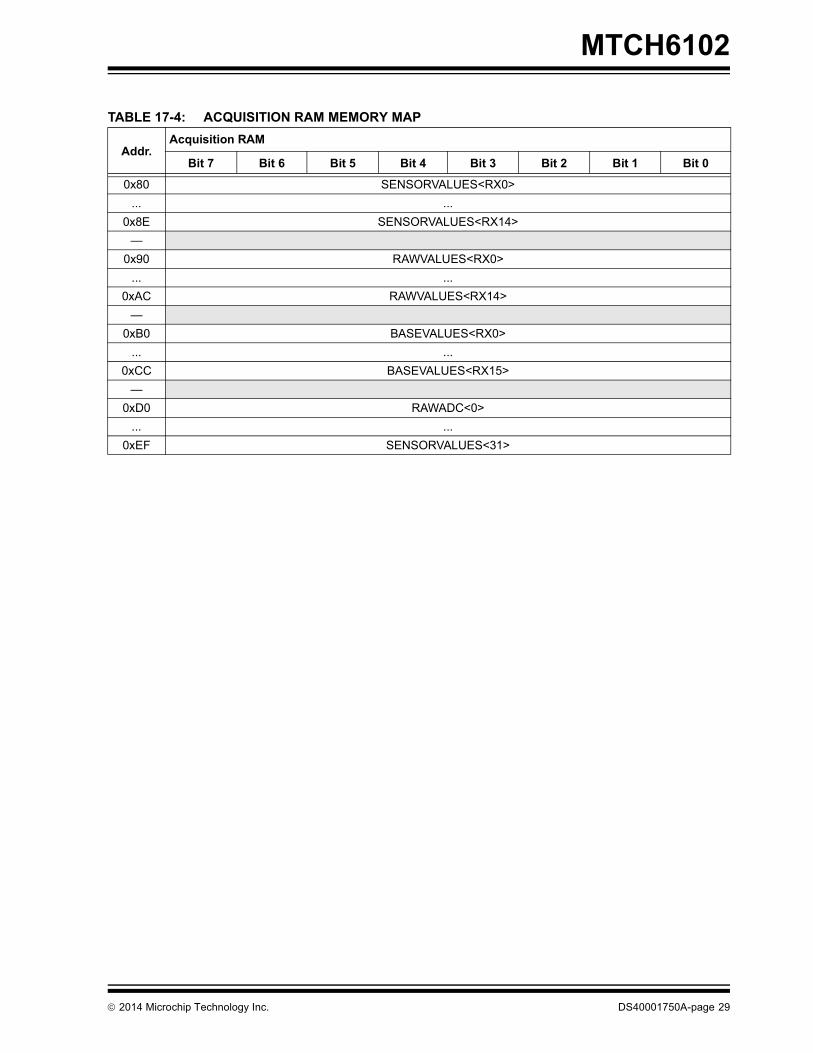
TABLE 17-4: ACQUISITION RAM MEMORY MAP
Addr.Acquisition RAM
Bit 7 Bit 6 Bit 5 Bit 4 Bit 3 Bit 2 Bit 1 Bit 0
0x80 SENSORVALUES<RX0>... ...
0x8E SENSORVALUES<RX14>—
0x90 RAWVALUES<RX0>... ...
0xAC RAWVALUES<RX14>—
0xB0 BASEVALUES<RX0>... ...
0xCC BASEVALUES<RX15>—
0xD0 RAWADC<0>... ...
0xEF SENSORVALUES<31>
2014 Microchip Technology Inc. DS40001750A-page 29
MTCH6102
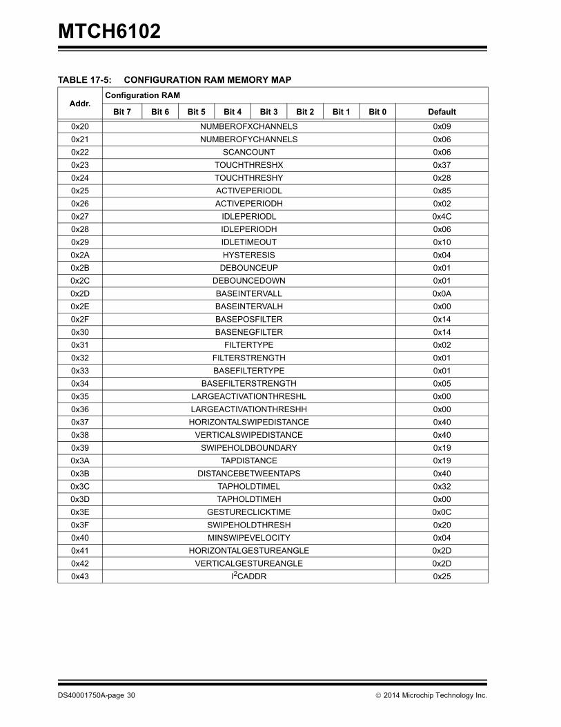
TABLE 17-5: CONFIGURATION RAM MEMORY MAP
Addr.Configuration RAM
Bit 7 Bit 6 Bit 5 Bit 4 Bit 3 Bit 2 Bit 1 Bit 0 Default
0x20 NUMBEROFXCHANNELS 0x090x21 NUMBEROFYCHANNELS 0x060x22 SCANCOUNT 0x060x23 TOUCHTHRESHX 0x370x24 TOUCHTHRESHY 0x280x25 ACTIVEPERIODL 0x850x26 ACTIVEPERIODH 0x020x27 IDLEPERIODL 0x4C0x28 IDLEPERIODH 0x060x29 IDLETIMEOUT 0x100x2A HYSTERESIS 0x040x2B DEBOUNCEUP 0x010x2C DEBOUNCEDOWN 0x010x2D BASEINTERVALL 0x0A0x2E BASEINTERVALH 0x000x2F BASEPOSFILTER 0x140x30 BASENEGFILTER 0x140x31 FILTERTYPE 0x020x32 FILTERSTRENGTH 0x010x33 BASEFILTERTYPE 0x010x34 BASEFILTERSTRENGTH 0x050x35 LARGEACTIVATIONTHRESHL 0x000x36 LARGEACTIVATIONTHRESHH 0x000x37 HORIZONTALSWIPEDISTANCE 0x400x38 VERTICALSWIPEDISTANCE 0x400x39 SWIPEHOLDBOUNDARY 0x190x3A TAPDISTANCE 0x190x3B DISTANCEBETWEENTAPS 0x400x3C TAPHOLDTIMEL 0x320x3D TAPHOLDTIMEH 0x000x3E GESTURECLICKTIME 0x0C0x3F SWIPEHOLDTHRESH 0x200x40 MINSWIPEVELOCITY 0x040x41 HORIZONTALGESTUREANGLE 0x2D0x42 VERTICALGESTUREANGLE 0x2D0x43 I2CADDR 0x25
DS40001750A-page 30 2014 Microchip Technology Inc.
MTCH6102
18.0 ELECTRICAL CHARACTERISTICS
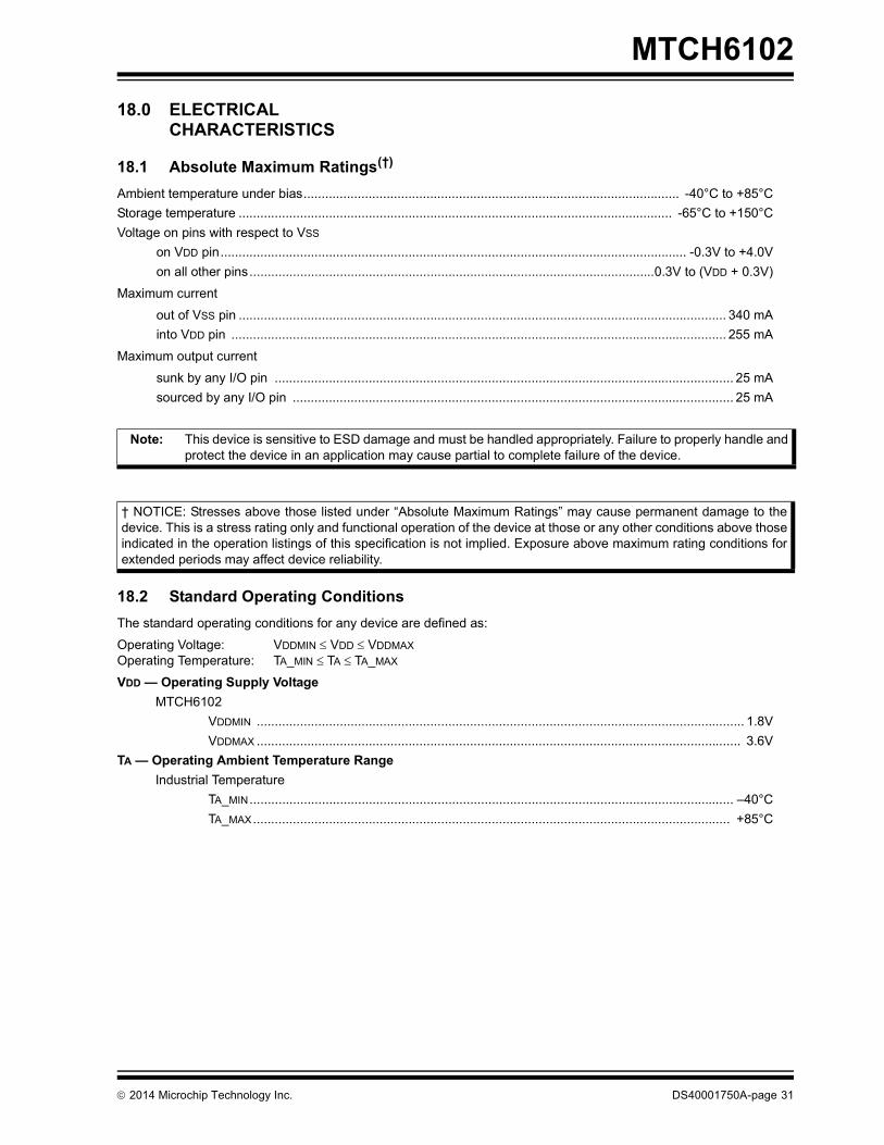
18.1 Absolute Maximum Ratings(†)
Ambient temperature under bias........................................................................................................ -40°C to +85°CStorage temperature ........................................................................................................................ -65°C to +150°CVoltage on pins with respect to VSS
on VDD pin................................................................................................................................. -0.3V to +4.0Von all other pins................................................................................................................0.3V to (VDD + 0.3V)
Maximum current
out of VSS pin ....................................................................................................................................... 340 mAinto VDD pin ......................................................................................................................................... 255 mA
Maximum output current
sunk by any I/O pin ............................................................................................................................... 25 mAsourced by any I/O pin .......................................................................................................................... 25 mA
18.2 Standard Operating ConditionsThe standard operating conditions for any device are defined as:
Operating Voltage: VDDMIN VDD VDDMAXOperating Temperature: TA_MIN TA TA_MAX
VDD — Operating Supply VoltageMTCH6102
VDDMIN ....................................................................................................................................... 1.8VVDDMAX ...................................................................................................................................... 3.6V
TA — Operating Ambient Temperature RangeIndustrial Temperature
TA_MIN...................................................................................................................................... –40°CTA_MAX.................................................................................................................................... +85°C
Note: This device is sensitive to ESD damage and must be handled appropriately. Failure to properly handle andprotect the device in an application may cause partial to complete failure of the device.
† NOTICE: Stresses above those listed under “Absolute Maximum Ratings” may cause permanent damage to thedevice. This is a stress rating only and functional operation of the device at those or any other conditions above thoseindicated in the operation listings of this specification is not implied. Exposure above maximum rating conditions forextended periods may affect device reliability.
2014 Microchip Technology Inc. DS40001750A-page 31
MTCH6102
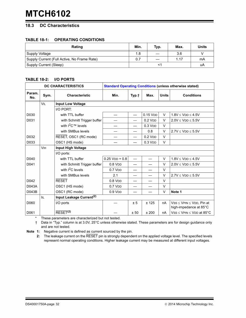
18.3 DC CharacteristicsTABLE 18-1: OPERATING CONDITIONSRating Min. Typ. Max. Units
Supply Voltage 1.8 — 3.6 VSupply Current (Full Active, No Frame Rate) 0.7 — 1.17 mASupply Current (Sleep) <1 uA
TABLE 18-2: I/O PORTSDC CHARACTERISTICS Standard Operating Conditions (unless otherwise stated)
Param.No. Sym. Characteristic Min. Typ.† Max. Units Conditions
VIL Input Low VoltageI/O PORT:
D030 with TTL buffer — — 0.15 VDD V 1.8V VDD 4.5VD031 with Schmitt Trigger buffer — — 0.2 VDD V 2.0V VDD 5.5V
with I2C™ levels — — 0.3 VDD Vwith SMBus levels — — 0.8 V 2.7V VDD 5.5V
D032 RESET, OSC1 (RC mode) — — 0.2 VDD VD033 OSC1 (HS mode) — — 0.3 VDD V
VIH Input High VoltageI/O ports:
D040 with TTL buffer 0.25 VDD + 0.8 — — V 1.8V VDD 4.5VD041 with Schmitt Trigger buffer 0.8 VDD — — V 2.0V VDD 5.5V
with I2C levels 0.7 VDD — — Vwith SMBus levels 2.1 — — V 2.7V VDD 5.5V
D042 RESET 0.8 VDD — — VD043A OSC1 (HS mode) 0.7 VDD — — VD043B OSC1 (RC mode) 0.9 VDD — — V Note 1
IIL Input Leakage Current(2)
D060 I/O ports — ± 5 ± 125 nA VSS VPIN VDD, Pin at high-impedance at 85°C
D061 RESET(2) — ± 50 ± 200 nA VSS VPIN VDD at 85°C* These parameters are characterized but not tested.† Data in “Typ.” column is at 3.0V, 25°C unless otherwise stated. These parameters are for design guidance only
and are not tested.Note 1: Negative current is defined as current sourced by the pin.
2: The leakage current on the RESET pin is strongly dependent on the applied voltage level. The specified levels represent normal operating conditions. Higher leakage current may be measured at different input voltages.
DS40001750A-page 32 2014 Microchip Technology Inc.
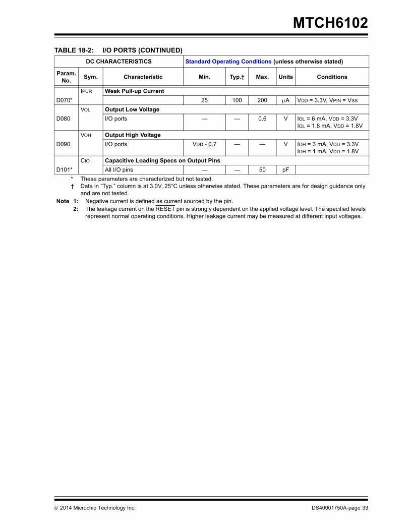
MTCH6102
IPUR Weak Pull-up CurrentD070* 25 100 200 A VDD = 3.3V, VPIN = VSS
VOL Output Low VoltageD080 I/O ports — — 0.6 V IOL = 6 mA, VDD = 3.3V
IOL = 1.8 mA, VDD = 1.8VVOH Output High Voltage
D090 I/O ports VDD - 0.7 — — V IOH = 3 mA, VDD = 3.3VIOH = 1 mA, VDD = 1.8V
CIO Capacitive Loading Specs on Output PinsD101* All I/O pins — — 50 pF
TABLE 18-2: I/O PORTS (CONTINUED)DC CHARACTERISTICS Standard Operating Conditions (unless otherwise stated)
Param.No. Sym. Characteristic Min. Typ.† Max. Units Conditions
* These parameters are characterized but not tested.† Data in “Typ.” column is at 3.0V, 25°C unless otherwise stated. These parameters are for design guidance only
and are not tested.Note 1: Negative current is defined as current sourced by the pin.
2: The leakage current on the RESET pin is strongly dependent on the applied voltage level. The specified levels represent normal operating conditions. Higher leakage current may be measured at different input voltages.
2014 Microchip Technology Inc. DS40001750A-page 33
MTCH6102
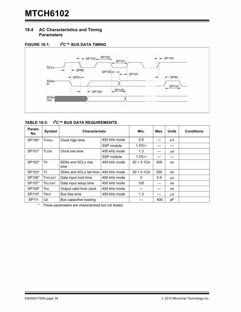
18.4 AC Characteristics and TimingParameters
FIGURE 18-1: I2C™ BUS DATA TIMING
TABLE 18-3: I2C™ BUS DATA REQUIREMENTSParam.
No. Symbol Characteristic Min. Max. Units Conditions
SP100* THIGH Clock high time 400 kHz mode 0.6 — s
SSP module 1.5TCY — —SP101* TLOW Clock low time 400 kHz mode 1.3 — s
SSP module 1.5TCY — —SP102* TR SDAx and SCLx rise
time400 kHz mode 20 + 0.1CB 300 ns
SP103* TF SDAx and SCLx fall time 400 kHz mode 20 + 0.1CB 250 nsSP106* THD:DAT Data input hold time 400 kHz mode 0 0.9 sSP107* TSU:DAT Data input setup time 400 kHz mode 100 — nsSP109* TAA Output valid from clock 400 kHz mode — — nsSP110* TBUF Bus free time 400 kHz mode 1.3 — sSP111 CB Bus capacitive loading — 400 pF
* These parameters are characterized but not tested.
SP90
SP91 SP92
SP100SP101
SP103
SP106SP107
SP109 SP109SP110
SP102
SCLx
SDAxIn
SDAxOut
DS40001750A-page 34 2014 Microchip Technology Inc.
MTCH6102
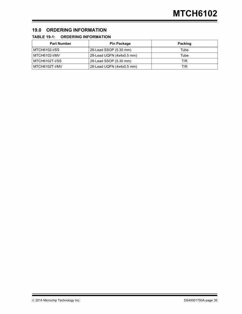
19.0 ORDERING INFORMATIONTABLE 19-1: ORDERING INFORMATION
Part Number Pin Package Packing
MTCH6102-I/SS 28-Lead SSOP (5.30 mm) TubeMTCH6102-I/MV 28-Lead UQFN (4x4x0.5 mm) TubeMTCH6102T-I/SS 28-Lead SSOP (5.30 mm) T/RMTCH6102T-I/MV 28-Lead UQFN (4x4x0.5 mm) T/R
2014 Microchip Technology Inc. DS40001750A-page 35
MTCH6102
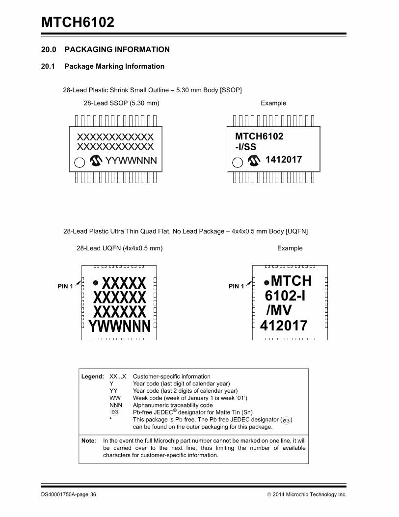
20.0 PACKAGING INFORMATION
20.1 Package Marking Information
Legend: XX...X Customer-specific informationY Year code (last digit of calendar year)YY Year code (last 2 digits of calendar year)WW Week code (week of January 1 is week ‘01’)NNN Alphanumeric traceability code Pb-free JEDEC® designator for Matte Tin (Sn)* This package is Pb-free. The Pb-free JEDEC designator ( )
can be found on the outer packaging for this package.
Note: In the event the full Microchip part number cannot be marked on one line, it willbe carried over to the next line, thus limiting the number of availablecharacters for customer-specific information.
3e
3e
28-Lead SSOP (5.30 mm) Example
28-Lead UQFN (4x4x0.5 mm) Example
PIN 1 PIN 1
MTCH6102
1412017-I/SS
MTCH6102-I/MV
412017
28-Lead Plastic Shrink Small Outline – 5.30 mm Body [SSOP]
28-Lead Plastic Ultra Thin Quad Flat, No Lead Package – 4x4x0.5 mm Body [UQFN]
DS40001750A-page 36 2014 Microchip Technology Inc.
MTCH6102
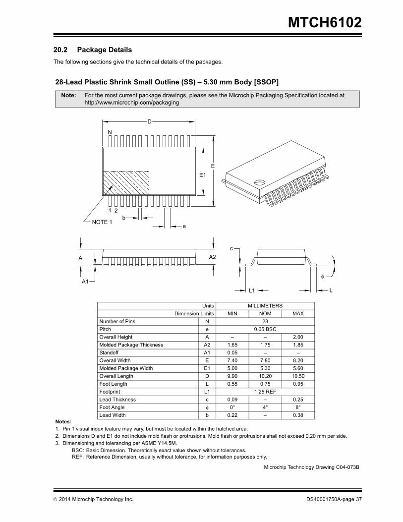
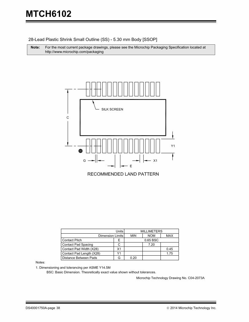
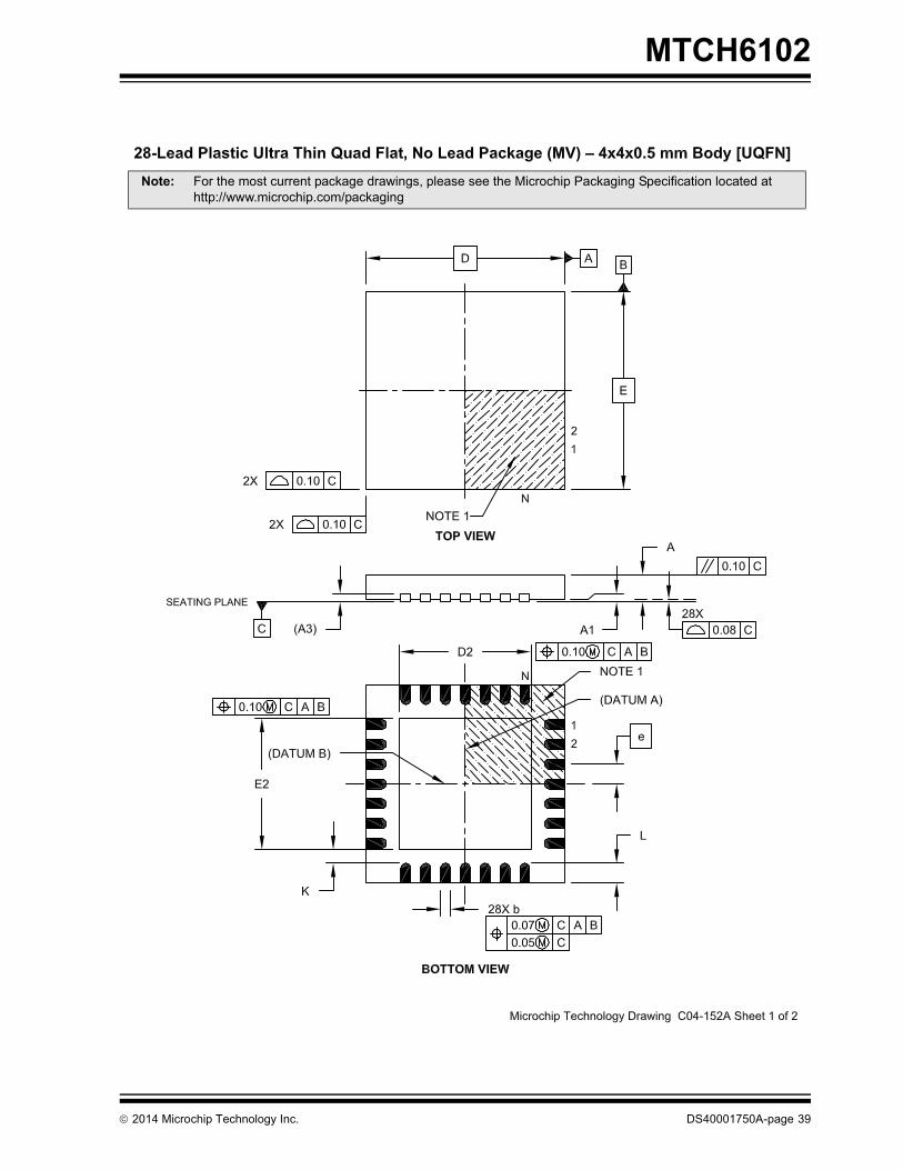
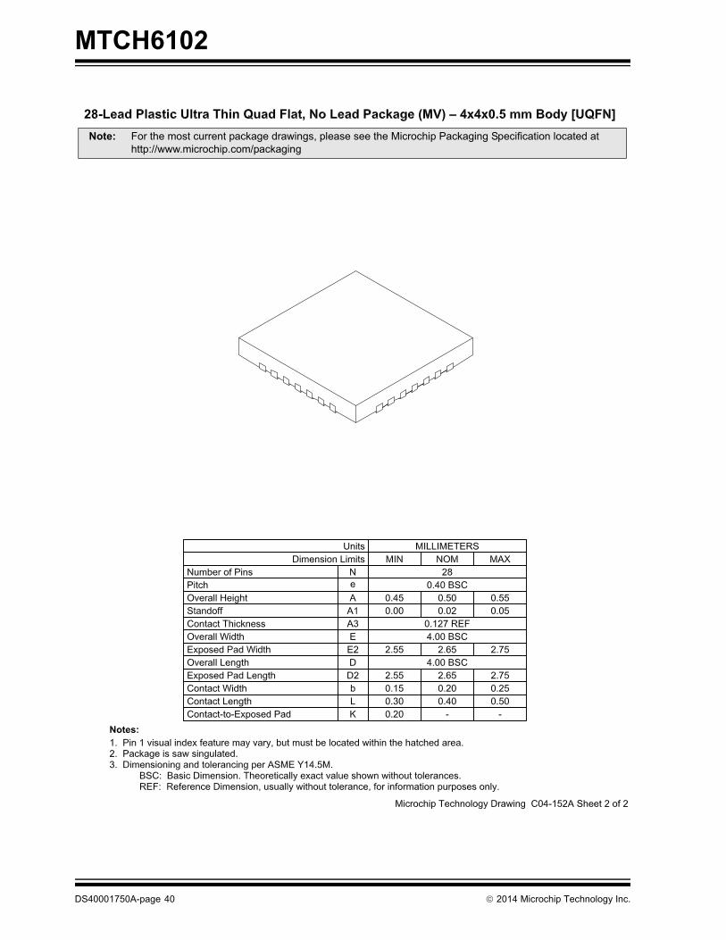
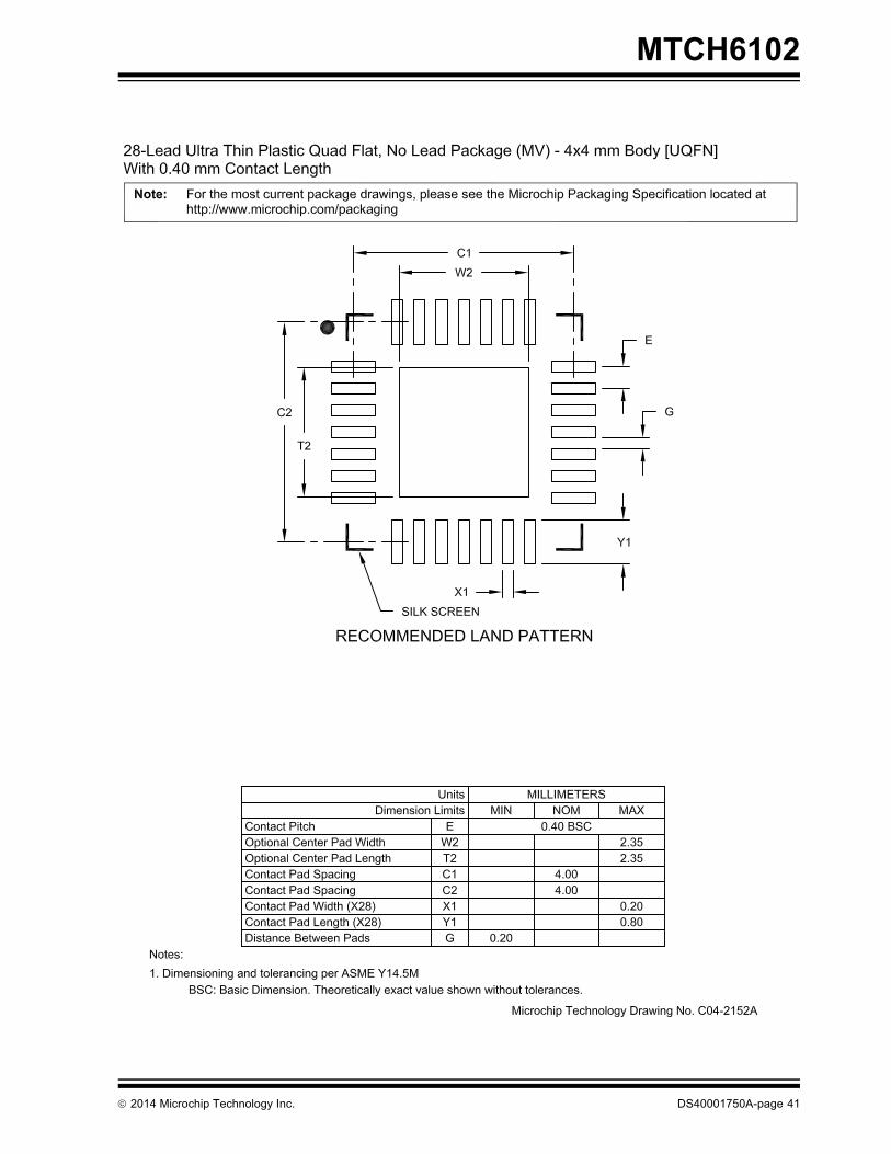
20.2 Package DetailsThe following sections give the technical details of the packages.���������� ��������������� ���������������� �!"���#
$ ��%�� ������ �!"�����# $�% �&"� �'��� ���(�)"&�'"!&�) �����& #�*�&����&� ���&�� #��� ���� ��' �!���!�����#�+��#����&�����"# �'��#�%��!�������&�"!���!�����#�%��!�������&�"!���!�!�������&� $� #������''� ��!�# �,� ��' �!���������#�&�� �������� �����+�-���.��
/�01 /�!�����' �!������� �� &������� $��&� ��" �!��*��*�&��"&�&�� ���� !��+21 � % � �� ���' �!���(�"!"�����*�&��"&�&�� ���� (�%�����%��'�&����"��! !������
$ �% 2���&� �'�!&��"�� �&���3�� �#��*���!(�� �! �! �&� �������������3������� ��%���&��������& #��&��&&144***�'����������'4��3�����
5��&! ��66��+�+����' �!����6�'�&! ��7 78� ��9
7"') ���%����! 7 �:��&�� ���.�/�08 �����; ���& � < < �������# #����3�� �����3� !! �� ���. ���. ��:.�&��#�%%� �� ���. < <8 �����=�#&� + ���� ��:� :������# #����3�� �=�#&� +� .��� .�,� .���8 �����6 ��&� � ���� ����� ���.�2��&�6 ��&� 6 ��.. ���. ���.2��&���& 6� ���.��+26 �#�����3� !! � ���� < ���.2��&����� � �> �> :>6 �#�=�#&� ) ���� < ��,:
LL1
cA2
A1
A
EE1
D
N
1 2
NOTE 1b
e
φ
�������� � �������� ���*��� 0����,/
2014 Microchip Technology Inc. DS40001750A-page 37
MTCH6102
Note: For the most current package drawings, please see the Microchip Packaging Specification located at http://www.microchip.com/packaging
DS40001750A-page 38 2014 Microchip Technology Inc.
MTCH6102
Note: For the most current package drawings, please see the Microchip Packaging Specification located at http://www.microchip.com/packaging
2014 Microchip Technology Inc. DS40001750A-page 39
MTCH6102
Note: For the most current package drawings, please see the Microchip Packaging Specification located at http://www.microchip.com/packaging
DS40001750A-page 40 2014 Microchip Technology Inc.
MTCH6102
2014 Microchip Technology Inc. DS40001750A-page 41
MTCH6102
APPENDIX A: DATA SHEET REVISION HISTORY
Revision A (03/2014)Initial release of the document.
DS40001750A-page 42 2014 Microchip Technology Inc.
2014 Microchip Technology Inc. DS40001750A-page 43
MTCH6102
THE MICROCHIP WEB SITEMicrochip provides online support via our WWW site atwww.microchip.com. This web site is used as a meansto make files and information easily available tocustomers. Accessible by using your favorite Internetbrowser, the web site contains the followinginformation:
• Product Support – Data sheets and errata, application notes and sample programs, design resources, user’s guides and hardware support documents, latest software releases and archived software
• General Technical Support – Frequently Asked Questions (FAQ), technical support requests, online discussion groups, Microchip consultant program member listing
• Business of Microchip – Product selector and ordering guides, latest Microchip press releases, listing of seminars and events, listings of Microchip sales offices, distributors and factory representatives
CUSTOMER CHANGE NOTIFICATION SERVICEMicrochip’s customer notification service helps keepcustomers current on Microchip products. Subscriberswill receive e-mail notification whenever there arechanges, updates, revisions or errata related to aspecified product family or development tool of interest.
To register, access the Microchip web site atwww.microchip.com. Under “Support”, click on“Customer Change Notification” and follow theregistration instructions.
CUSTOMER SUPPORTUsers of Microchip products can receive assistancethrough several channels:
• Distributor or Representative• Local Sales Office• Field Application Engineer (FAE)• Technical Support
Customers should contact their distributor,representative or Field Application Engineer (FAE) forsupport. Local sales offices are also available to helpcustomers. A listing of sales offices and locations isincluded in the back of this document.
Technical support is available through the web siteat: http://microchip.com/support
Note the following details of the code protection feature on Microchip devices:• Microchip products meet the specification contained in their particular Microchip Data Sheet.
• Microchip believes that its family of products is one of the most secure families of its kind on the market today, when used in the intended manner and under normal conditions.
• There are dishonest and possibly illegal methods used to breach the code protection feature. All of these methods, to our knowledge, require using the Microchip products in a manner outside the operating specifications contained in Microchip’s Data Sheets. Most likely, the person doing so is engaged in theft of intellectual property.
• Microchip is willing to work with the customer who is concerned about the integrity of their code.
• Neither Microchip nor any other semiconductor manufacturer can guarantee the security of their code. Code protection does not mean that we are guaranteeing the product as “unbreakable.”
Code protection is constantly evolving. We at Microchip are committed to continuously improving the code protection features of ourproducts. Attempts to break Microchip’s code protection feature may be a violation of the Digital Millennium Copyright Act. If such actsallow unauthorized access to your software or other copyrighted work, you may have a right to sue for relief under that Act.
Information contained in this publication regarding deviceapplications and the like is provided only for your convenienceand may be superseded by updates. It is your responsibility toensure that your application meets with your specifications.MICROCHIP MAKES NO REPRESENTATIONS ORWARRANTIES OF ANY KIND WHETHER EXPRESS ORIMPLIED, WRITTEN OR ORAL, STATUTORY OROTHERWISE, RELATED TO THE INFORMATION,INCLUDING BUT NOT LIMITED TO ITS CONDITION,QUALITY, PERFORMANCE, MERCHANTABILITY ORFITNESS FOR PURPOSE. Microchip disclaims all liabilityarising from this information and its use. Use of Microchipdevices in life support and/or safety applications is entirely atthe buyer’s risk, and the buyer agrees to defend, indemnify andhold harmless Microchip from any and all damages, claims,suits, or expenses resulting from such use. No licenses areconveyed, implicitly or otherwise, under any Microchipintellectual property rights.
DS40001750A-page 44
QUALITY MANAGEMENT SYSTEM CERTIFIED BY DNV
== ISO/TS 16949 ==
Trademarks
The Microchip name and logo, the Microchip logo, dsPIC, FlashFlex, KEELOQ, KEELOQ logo, MPLAB, PIC, PICmicro, PICSTART, PIC32 logo, rfPIC, SST, SST Logo, SuperFlash and UNI/O are registered trademarks of Microchip Technology Incorporated in the U.S.A. and other countries.
FilterLab, Hampshire, HI-TECH C, Linear Active Thermistor, MTP, SEEVAL and The Embedded Control Solutions Company are registered trademarks of Microchip Technology Incorporated in the U.S.A.
Silicon Storage Technology is a registered trademark of Microchip Technology Inc. in other countries.
Analog-for-the-Digital Age, Application Maestro, BodyCom, chipKIT, chipKIT logo, CodeGuard, dsPICDEM, dsPICDEM.net, dsPICworks, dsSPEAK, ECAN, ECONOMONITOR, FanSense, HI-TIDE, In-Circuit Serial Programming, ICSP, Mindi, MiWi, MPASM, MPF, MPLAB Certified logo, MPLIB, MPLINK, mTouch, Omniscient Code Generation, PICC, PICC-18, PICDEM, PICDEM.net, PICkit, PICtail, REAL ICE, rfLAB, Select Mode, SQI, Serial Quad I/O, Total Endurance, TSHARC, UniWinDriver, WiperLock, ZENA and Z-Scale are trademarks of Microchip Technology Incorporated in the U.S.A. and other countries.
SQTP is a service mark of Microchip Technology Incorporated in the U.S.A.
GestIC and ULPP are registered trademarks of Microchip Technology Germany II GmbH & Co. KG, a subsidiary of Microchip Technology Inc., in other countries.
All other trademarks mentioned herein are property of their respective companies.
© 2014, Microchip Technology Incorporated, Printed in the U.S.A., All Rights Reserved.
Printed on recycled paper.
ISBN: 978-1-63276-043-2
Microchip received ISO/TS-16949:2009 certification for its worldwide
2014 Microchip Technology Inc.
headquarters, design and wafer fabrication facilities in Chandler and Tempe, Arizona; Gresham, Oregon and design centers in California and India. The Company’s quality system processes and procedures are for its PIC® MCUs and dsPIC® DSCs, KEELOQ® code hopping devices, Serial EEPROMs, microperipherals, nonvolatile memory and analog products. In addition, Microchip’s quality system for the design and manufacture of development systems is ISO 9001:2000 certified.
2014 Microchip Technology Inc. DS40001750A-page 45
AMERICASCorporate Office2355 West Chandler Blvd.Chandler, AZ 85224-6199Tel: 480-792-7200 Fax: 480-792-7277Technical Support: http://www.microchip.com/supportWeb Address: www.microchip.comAtlantaDuluth, GA Tel: 678-957-9614 Fax: 678-957-1455Austin, TXTel: 512-257-3370 BostonWestborough, MA Tel: 774-760-0087 Fax: 774-760-0088ChicagoItasca, IL Tel: 630-285-0071 Fax: 630-285-0075ClevelandIndependence, OH Tel: 216-447-0464 Fax: 216-447-0643DallasAddison, TX Tel: 972-818-7423 Fax: 972-818-2924DetroitNovi, MI Tel: 248-848-4000Houston, TX Tel: 281-894-5983IndianapolisNoblesville, IN Tel: 317-773-8323Fax: 317-773-5453Los AngelesMission Viejo, CA Tel: 949-462-9523 Fax: 949-462-9608New York, NY Tel: 631-435-6000San Jose, CA Tel: 408-735-9110Canada - TorontoTel: 905-673-0699 Fax: 905-673-6509
ASIA/PACIFICAsia Pacific OfficeSuites 3707-14, 37th FloorTower 6, The GatewayHarbour City, KowloonHong KongTel: 852-2943-5100Fax: 852-2401-3431Australia - SydneyTel: 61-2-9868-6733Fax: 61-2-9868-6755China - BeijingTel: 86-10-8569-7000 Fax: 86-10-8528-2104China - ChengduTel: 86-28-8665-5511Fax: 86-28-8665-7889China - ChongqingTel: 86-23-8980-9588Fax: 86-23-8980-9500China - HangzhouTel: 86-571-8792-8115 Fax: 86-571-8792-8116China - Hong Kong SARTel: 852-2943-5100 Fax: 852-2401-3431China - NanjingTel: 86-25-8473-2460Fax: 86-25-8473-2470China - QingdaoTel: 86-532-8502-7355Fax: 86-532-8502-7205China - ShanghaiTel: 86-21-5407-5533 Fax: 86-21-5407-5066China - ShenyangTel: 86-24-2334-2829Fax: 86-24-2334-2393China - ShenzhenTel: 86-755-8864-2200 Fax: 86-755-8203-1760China - WuhanTel: 86-27-5980-5300Fax: 86-27-5980-5118China - XianTel: 86-29-8833-7252Fax: 86-29-8833-7256China - XiamenTel: 86-592-2388138 Fax: 86-592-2388130China - ZhuhaiTel: 86-756-3210040 Fax: 86-756-3210049
ASIA/PACIFICIndia - BangaloreTel: 91-80-3090-4444 Fax: 91-80-3090-4123India - New DelhiTel: 91-11-4160-8631Fax: 91-11-4160-8632India - PuneTel: 91-20-3019-1500Japan - OsakaTel: 81-6-6152-7160 Fax: 81-6-6152-9310Japan - TokyoTel: 81-3-6880- 3770 Fax: 81-3-6880-3771Korea - DaeguTel: 82-53-744-4301Fax: 82-53-744-4302Korea - SeoulTel: 82-2-554-7200Fax: 82-2-558-5932 or 82-2-558-5934Malaysia - Kuala LumpurTel: 60-3-6201-9857Fax: 60-3-6201-9859Malaysia - PenangTel: 60-4-227-8870Fax: 60-4-227-4068Philippines - ManilaTel: 63-2-634-9065Fax: 63-2-634-9069SingaporeTel: 65-6334-8870Fax: 65-6334-8850Taiwan - Hsin ChuTel: 886-3-5778-366Fax: 886-3-5770-955Taiwan - KaohsiungTel: 886-7-213-7830Taiwan - TaipeiTel: 886-2-2508-8600 Fax: 886-2-2508-0102Thailand - BangkokTel: 66-2-694-1351Fax: 66-2-694-1350
EUROPEAustria - WelsTel: 43-7242-2244-39Fax: 43-7242-2244-393Denmark - CopenhagenTel: 45-4450-2828 Fax: 45-4485-2829France - ParisTel: 33-1-69-53-63-20 Fax: 33-1-69-30-90-79Germany - DusseldorfTel: 49-2129-3766400Germany - MunichTel: 49-89-627-144-0 Fax: 49-89-627-144-44Germany - PforzheimTel: 49-7231-424750Italy - Milan Tel: 39-0331-742611 Fax: 39-0331-466781Italy - VeniceTel: 39-049-7625286 Netherlands - DrunenTel: 31-416-690399 Fax: 31-416-690340Poland - WarsawTel: 48-22-3325737 Spain - MadridTel: 34-91-708-08-90Fax: 34-91-708-08-91Sweden - StockholmTel: 46-8-5090-4654UK - WokinghamTel: 44-118-921-5800Fax: 44-118-921-5820
Worldwide Sales and Service
03/25/14