mrf24j40ma data sheet - microchipww1.microchip.com/downloads/en/devicedoc/70329b.pdf · mrf24j40ma...
TRANSCRIPT

© 2008 Microchip Technology Inc. DS70329B
MRF24J40MAData Sheet
2.4 GHz IEEE Std. 802.15.4™RF Transceiver Module
Note the following details of the code protection feature on Microchip devices:• Microchip products meet the specification contained in their particular Microchip Data Sheet.
• Microchip believes that its family of products is one of the most secure families of its kind on the market today, when used in the intended manner and under normal conditions.
• There are dishonest and possibly illegal methods used to breach the code protection feature. All of these methods, to our knowledge, require using the Microchip products in a manner outside the operating specifications contained in Microchip’s Data Sheets. Most likely, the person doing so is engaged in theft of intellectual property.
• Microchip is willing to work with the customer who is concerned about the integrity of their code.
• Neither Microchip nor any other semiconductor manufacturer can guarantee the security of their code. Code protection does not mean that we are guaranteeing the product as “unbreakable.”
Code protection is constantly evolving. We at Microchip are committed to continuously improving the code protection features of ourproducts. Attempts to break Microchip’s code protection feature may be a violation of the Digital Millennium Copyright Act. If such actsallow unauthorized access to your software or other copyrighted work, you may have a right to sue for relief under that Act.
Information contained in this publication regarding deviceapplications and the like is provided only for your convenienceand may be superseded by updates. It is your responsibility toensure that your application meets with your specifications.MICROCHIP MAKES NO REPRESENTATIONS ORWARRANTIES OF ANY KIND WHETHER EXPRESS ORIMPLIED, WRITTEN OR ORAL, STATUTORY OROTHERWISE, RELATED TO THE INFORMATION,INCLUDING BUT NOT LIMITED TO ITS CONDITION,QUALITY, PERFORMANCE, MERCHANTABILITY ORFITNESS FOR PURPOSE. Microchip disclaims all liabilityarising from this information and its use. Use of Microchipdevices in life support and/or safety applications is entirely atthe buyer’s risk, and the buyer agrees to defend, indemnify andhold harmless Microchip from any and all damages, claims,suits, or expenses resulting from such use. No licenses areconveyed, implicitly or otherwise, under any Microchipintellectual property rights.
DS70329B-page ii
Trademarks
The Microchip name and logo, the Microchip logo, Accuron, dsPIC, KEELOQ, KEELOQ logo, MPLAB, PIC, PICmicro, PICSTART, rfPIC, SmartShunt and UNI/O are registered trademarks of Microchip Technology Incorporated in the U.S.A. and other countries.
FilterLab, Linear Active Thermistor, MXDEV, MXLAB, SEEVAL, SmartSensor and The Embedded Control Solutions Company are registered trademarks of Microchip Technology Incorporated in the U.S.A.
Analog-for-the-Digital Age, Application Maestro, CodeGuard, dsPICDEM, dsPICDEM.net, dsPICworks, dsSPEAK, ECAN, ECONOMONITOR, FanSense, In-Circuit Serial Programming, ICSP, ICEPIC, Mindi, MiWi, MPASM, MPLAB Certified logo, MPLIB, MPLINK, mTouch, PICkit, PICDEM, PICDEM.net, PICtail, PIC32 logo, PowerCal, PowerInfo, PowerMate, PowerTool, REAL ICE, rfLAB, Select Mode, Total Endurance, WiperLock and ZENA are trademarks of Microchip Technology Incorporated in the U.S.A. and other countries.
SQTP is a service mark of Microchip Technology Incorporated in the U.S.A.
All other trademarks mentioned herein are property of their respective companies.
© 2008, Microchip Technology Incorporated, Printed in the U.S.A., All Rights Reserved.
Printed on recycled paper.
© 2008 Microchip Technology Inc.
Microchip received ISO/TS-16949:2002 certification for its worldwide headquarters, design and wafer fabrication facilities in Chandler and Tempe, Arizona; Gresham, Oregon and design centers in California and India. The Company’s quality system processes and procedures are for its PIC® MCUs and dsPIC® DSCs, KEELOQ® code hopping devices, Serial EEPROMs, microperipherals, nonvolatile memory and analog products. In addition, Microchip’s quality system for the design and manufacture of development systems is ISO 9001:2000 certified.
MRF24J40MA2.4 GHz IEEE Std. 802.15.4™ RF Transceiver Module
Features:• IEEE Std. 802.15.4™ Compliant RF Transceiver• Supports ZigBee®, MiWi™, MiWi™ P2P and
Proprietary Wireless Networking Protocols• Small Size: 0.7” x 1.1” (17.8 mm x 27.9 mm),
Surface Mountable• Integrated Crystal, Internal Voltage Regulator,
Matching Circuitry and PCB Antenna• Easy Integration into Final Product – Minimize
Product Development, Quicker Time to Market• Radio Regulation Certification for United States
(FCC), Canada (IC) and Europe (ETSI)• Compatible with Microchip Microcontroller
Families (PIC16F, PIC18F, PIC24F/H, dsPIC33 and PIC32)
• Up to 400 ft. Range
Operational:• Operating Voltage: 2.4-3.6V (3.3V typical)• Temperature Range: -40°C to +85°C Industrial• Simple, Four-Wire SPI Interface• Low-Current Consumption:
- RX mode: 19 mA (typical)- TX mode: 23 mA (typical)- Sleep: 2 μA (typical)
RF/Analog Features:• ISM Band 2.405-2.48 GHz Operation• Data Rate: 250 kbps• -94 dBm Typical Sensitivity with +5 dBm
Maximum Input Level• +0 dBm Typical Output Power with
36 dB TX Power Control Range• Integrated Low Phase Noise VCO, Frequency
Synthesizer and PLL Loop Filter• Digital VCO and Filter Calibration• Integrated RSSI ADC and I/Q DACs• Integrated LDO• High Receiver and RSSI Dynamic Range
MAC/Baseband Features:• Hardware CSMA-CA Mechanism, Automatic ACK
Response and FCS Check• Independent Beacon, Transmit and GTS FIFO• Supports all CCA modes and RSS/LQI• Automatic Packet Retransmit Capable• Hardware Security Engine (AES-128) with CTR,
CCM and CBC-MAC modes• Supports Encryption and Decryption for MAC
Sublayer and Upper Layer
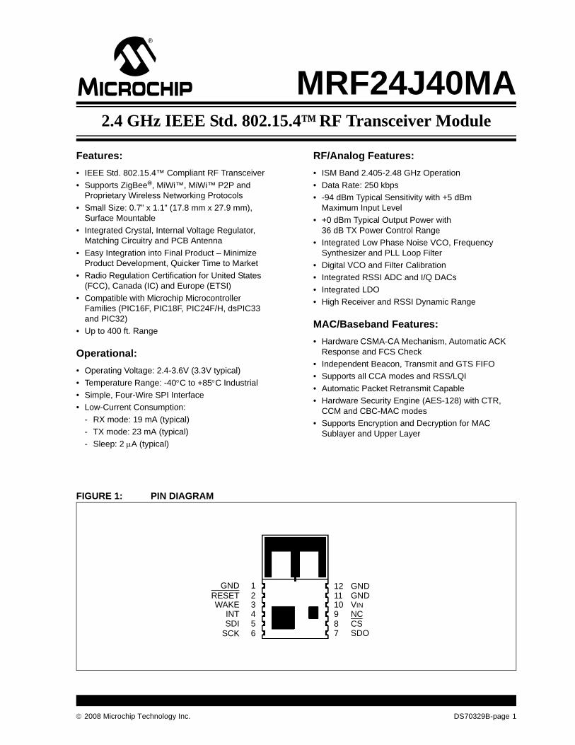
FIGURE 1: PIN DIAGRAM
23456
1
7
VIN
GND
8910
RESETWAKE
SDOSDI
SCKCSNC
GND
INT
1211 GND
© 2008 Microchip Technology Inc. DS70329B-page 1
MRF24J40MA
Table of Contents 1.0 Device Overview .......................................................................................................................................................................... 32.0 Circuit Description ........................................................................................................................................................................ 73.0 Regulatory Approval................................................................................................................................................................... 154.0 Electrical Characteristics ............................................................................................................................................................ 19Appendix A: Revision History............................................................................................................................................................... 21Index .................................................................................................................................................................................................... 23The Microchip Web Site ....................................................................................................................................................................... 25Customer Change Notification Service ................................................................................................................................................ 25Customer Support ................................................................................................................................................................................ 25Reader Response ................................................................................................................................................................................ 26Product Identification System............................................................................................................................................................... 27TO OUR VALUED CUSTOMERSIt is our intention to provide our valued customers with the best documentation possible to ensure successful use of your Microchipproducts. To this end, we will continue to improve our publications to better suit your needs. Our publications will be refined andenhanced as new volumes and updates are introduced. If you have any questions or comments regarding this publication, please contact the Marketing Communications Department viaE-mail at [email protected] or fax the Reader Response Form in the back of this data sheet to (480) 792-4150. Wewelcome your feedback.
Most Current Data SheetTo obtain the most up-to-date version of this data sheet, please register at our Worldwide Web site at:
http://www.microchip.comYou can determine the version of a data sheet by examining its literature number found on the bottom outside corner of any page.The last character of the literature number is the version number, (e.g., DS30000A is version A of document DS30000).
ErrataAn errata sheet, describing minor operational differences from the data sheet and recommended workarounds, may exist for currentdevices. As device/documentation issues become known to us, we will publish an errata sheet. The errata will specify the revisionof silicon and revision of document to which it applies.To determine if an errata sheet exists for a particular device, please check with one of the following:• Microchip’s Worldwide Web site; http://www.microchip.com• Your local Microchip sales office (see last page)When contacting a sales office, please specify which device, revision of silicon and data sheet (include literature number) you areusing.
Customer Notification SystemRegister on our web site at www.microchip.com to receive the most current information on all of our products.
DS70329B-page 2 © 2008 Microchip Technology Inc.

MRF24J40MA
1.0 DEVICE OVERVIEWThe MRF24J40MA is a 2.4 GHz IEEE Std. 802.15.4™compliant, surface mount module with integratedcrystal, internal voltage regulator, matching circuitryand PCB antenna. The MRF24J40MA module oper-ates in the non-licensed 2.4 GHz frequency band andis FCC, IC and ETSI compliant. The integrated moduledesign frees the integrator from extensive RF andantenna design, and regulatory compliance testing,allowing quicker time to market.
The MRF24J40MA module is compatible withMicrochip’s ZigBee®, MiWi™ and MiWi P2P softwarestacks. Each software stack is available as a freedownload, including source code, from the Microchipweb site http://www.microchip.com/wireless.
The MRF24J40MA module has received regulatoryapprovals for modular devices in the United States(FCC), Canada (IC) and Europe (ETSI). Modularapproval removes the need for expensive RF andantenna design and allows the end user to place the
MRF24J40MA module inside a finished product andnot require regulatory testing for an intentional radiator(RF transmitter). See Section 3.0 “RegulatoryApproval” for specific requirements to be followed bythe integrator.
1.1 Interface DescriptionFigure 1-1 shows a simplified block diagram of theMRF24J40MA module. The module is based on theMicrochip Technology MRF24J40 IEEE 802.15.4™2.4 GHz RF Transceiver IC. The module interfaces tomany popular Microchip PIC® microcontrollers via a4-wire serial SPI interface, interrupt, wake, Reset,power and ground, as shown in Figure 1-2. Table 1-1provides the pin descriptions.
Data communications with the MRF24J40MA moduleare documented in the “MRF24J40 IEEE 802.15.4™2.4 GHz RF Transceiver Data Sheet” (DS39776). Referto the MRF24J40 Data Sheet for specific serialinterface protocol and register definitions.
FIGURE 1-1: MRF24J40MA BLOCK DIAGRAM
PCBAntenna
MatchingCircuitry
Physical MAC
Interface
PowerManagement
SPI
20 MHzCrystal
DigitalI/O
Power
MRF24J40MA IEEE Std. 802.15.4™ Module
MRF24J40
© 2008 Microchip Technology Inc. DS70329B-page 3

MRF24J40MA
TABLE 1-1: PIN DESCRIPTIONFIGURE 1-2: MICROCONTROLLER TO MRF24J40MA INTERFACE
Pin Symbol Type Description
1 GND Power Ground
2 RESET DI Global hardware Reset pin3 WAKE DI External wake-up trigger4 INT DO Interrupt pin to microcontroller5 SDI DI Serial interface data input 6 SCK DI Serial interface clock7 SDO DO Serial interface data output from MRF24J40
8 CS DI Serial interface enable9 NC — No connection (allow pin to float; do not connect signal)
10 VIN Power Power supply11 GND Ground Ground12 GND Ground Ground
Legend: Pin type abbreviation: D = Digital, I = Input, O = Output
SDO
I/O
SDI
SCK
INTx
MRF24J40MA
CS
SDI
SDO
SCK
INT
I/O WAKE
VIN
GND
PIC® MCU
I/O RESET
DS70329B-page 4 © 2008 Microchip Technology Inc.

MRF24J40MA
1.2 Mounting DetailsThe MRF24J40MA is a surface mountable module.Module dimensions are shown in Figure 1-3. Themodule Printed Circuit Board (PCB) is 0.032" thick withcastellated mounting points on the edge. Figure 1-4 isa recommended host PCB footprint for theMRF24J40MA.The MRF24J40MA has an integrated PCB antenna.For the best performance, follow the mounting detailsshown in Figure 1-5. It is recommended that themodule be mounted on the edge of the host PCB, andan area around the antenna, approximately 1.2", bekept clear of metal objects. A host PCB ground planearound the MRF24J40MA acts as a counterpoise to thePCB antenna. It is recommended to extend the groundplane at least 0.4" around the module.
FIGURE 1-3: MODULE DETAILS
FIGURE 1-4: RECOMMENDED PCB FOOTPRINT
© 2008 Microchip Technology Inc. DS70329B-page 5

MRF24J40MA
FIGURE 1-5: MOUNTING DETAILS0.470”
Edge of PCB
Keep area around antenna(approximately 1.2 inches)clear of metallic structuresfor best performance
PCB Ground Plane (Counterpoise)Extend as far as possible to
the sides and below the module(at least 0.4 inches on each side)
for best performance
0.4”
0.4” 0.4”
1.2”
1.2”
DS70329B-page 6 © 2008 Microchip Technology Inc.

MRF24J40MA
2.0 CIRCUIT DESCRIPTIONThe MRF24J40MA is a complete 2.4 GHz IEEEStd. 802.15.4™ compliant surface mount module withintegrated crystal, internal voltage regulator, matchingcircuitry and PCB antenna. The MRF24J40MA moduleinterfaces to many popular Microchip PIC micro-controllers via a 4-wire serial SPI interface, interrupt,wake, Reset, power and ground. Data communicationswith the MRF24J40MA module are documented in the“MRF24J40 IEEE 802.15.4™ 2.4 GHz RF TransceiverData Sheet” (DS39776). Refer to the MRF24J40 DataSheet for specific serial interface protocol and registerdefinitions.
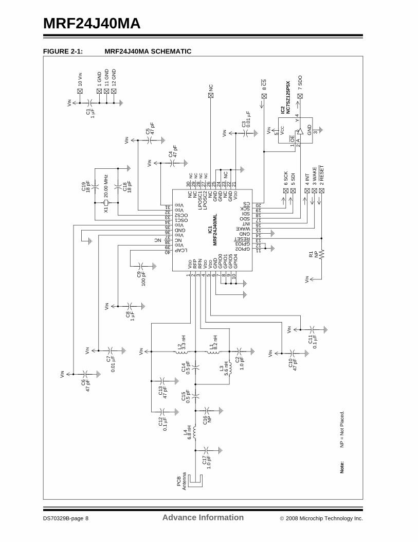
2.1 SchematicA schematic diagram of the module is shown inFigure 2-1 and the Bill of Materials (BOM) is shown inTable 2-1.
The MRF24J40MA module is based on the MicrochipTechnology MRF24J40 IEEE 802.15.4™ 2.4 GHz RFTransceiver IC. The serial I/O (SCK, SDI, SDO andCS), RESET, WAKE and INT pins are brought out tothe module pins. The SDO signal is tri-state buffered byIC2 to solve a silicon errata, where the SDO signaldoes not release to a high-impedance state, after theCS pin returns to its inactive state. Crystal, X1, is a20 MHz crystal with a frequency tolerance of±10 ppm @ 25°C to meet the IEEE Std. 802.15.4symbol rate tolerance of ±40 ppm. A balun is formed bycomponents: L1, L3, C2 and C14. L2 is an RF chokeand pull-up for the RFP and RFN pins on theMRF24J40. C15 is a DC block capacitor. A low-passfilter is formed by components: L4, C16 and C17. Theremaining capacitors provide RF and digital bypass.
© 2008 Microchip Technology Inc. Advance Information DS70329B-page 7
MRF24J40MA
FIGURE 2-1: MRF24J40MA SCHEMATICVD
D1
RFP
2R
FN3
VD
D4
VD
D5
GN
D6
GP
IO0
7G
PIO
18
GP
IO5
9G
PIO
410
NC
30N
C29
LPO
SC
128
LPO
SC
227
NC
26G
ND
25G
ND
24N
C23
GN
D22
VD
D21
IC1
GPIO2 11GPIO3 12RESET 13GND 14WAKE 15INT 16SDO 17SDI 18SCK 19CS 20
40393837363534333231
LCAPVDDNC
VDDGNDVDD
OSC1OCS2
VDDVDD
MR
F24J
40/M
L
NC
NC
NC
NC
NC NC
C10
47 p
F
VIN
C11
0.1
μF
VIN
L2 3.3
nH
L1 8.2
nH
VIN
C2
1.0
pF
L35.
6 nH
C14
0.5
pF
C13
47 p
FC
120.
1 μF
C15
0.5
pF
C16 NP
C17
1.0
pF
PC
BA
nten
naL4
6.8
nH
VIN
2 R
ES
ET
4 IN
T3
WA
KE
5 S
DI
6 S
CK
8 C
S
NC
OE
A
VIN
GN
D
Y
VC
C
1 2
IC2
NC
7SZ1
25P5
X
7 S
DO
35
4
C3
0.01
μF
VIN
R1
NP
12 G
ND
1 G
ND
11 G
ND
10 V
IN
VIN
C1
1 μF
C6
47 p
F
VIN
C4
47 p
F
VIN
C5
47 p
F
VIN
C18
18 p
F
C19
18 p
F
X1
20.0
0 M
Hz
C9
100
pF
C7
0.01
μF
VIN
C8
1 μF
VIN
Not
e:N
P =
Not
Pla
ced.
DS70329B-page 8 Advance Information © 2008 Microchip Technology Inc.

MRF24J40MA
TABLE 2-1: MRJ24J40MA BILL OF MATERIALSDesignator Description Manufacturer Part NumberC1 Chip Capacitor 0402 X5R 1U Murata GRM155R60J105ME19DC2 Chip Capacitor 0402 COG 1.0P Murata GRM1555C1H1R0CZ01DC3 Chip Capacitor 0402 X7R 10N Murata GRM155R71E103KA01DC4 Chip Capacitor 0402 COG 47P Murata GRM1555C1H470JZ01DC5 Chip Capacitor 0402 COG 47P Murata GRM1555C1H470JZ01DC6 Chip Capacitor 0402 COG 47P Murata GRM1555C1H470JZ01DC7 Chip Capacitor 0402 X7R 10N Murata GRM155R71E103KA01DC8 Chip Capacitor 0402 X5R 1U Murata GRM155R60J105ME19DC9 Chip Capacitor 0402 COG 100P Murata GRM1555C1H101JZ01D
C10 Chip Capacitor 0402 COG 47P Murata GRM1555C1H470JZ01DC11 Chip Capacitor 0402 X5R 100N Murata GRM155R61A104KA01DC12 Chip Capacitor 0402 X5R 100N Murata GRM155R61A104KA01DC13 Chip Capacitor 0402 COG 47P Murata GRM1555C1H470JZ01DC14 Chip Capacitor 0402 COG 0.5P Murata GRM1555C1HR50CZ01DC15 Chip Capacitor 0402 COG 0.5P Murata GRM1555C1HR50CZ01DC16 Not PlacedC17 Chip Capacitor 0402 COG 1.0P Murata GRM1555C1H1R0CZ01DC18 Chip Capacitor 0402 COG 18P Murata GRM1555C1H180JZ01DC19 Chip Capacitor 0402 COG 18P Murata GRM1555C1H180JZ01DIC1 IEEE 802.15.4™ RF Transceiver Microchip MRF24J40-I/MLIC2 Buffer, SC70 Package Fairchild NC7SZ125P5XL1 Chip Inductor 0402 8.2N Panasonic ELJ-RF8N2JFBL2 Chip Inductor 0402 3.3N Panasonic ELJ-RF3N3DFBL3 Chip Inductor 0402 5.6N Panasonic ELJ-RF5N6DFBL4 Chip Inductor 0402 6.8N Panasonic ELJ-RF6N8JFBR1 Not PlacedX1 20 MHz Crystal Abracon ABM8-156-20.0000MHZ-T
© 2008 Microchip Technology Inc. Advance Information DS70329B-page 9
MRF24J40MA
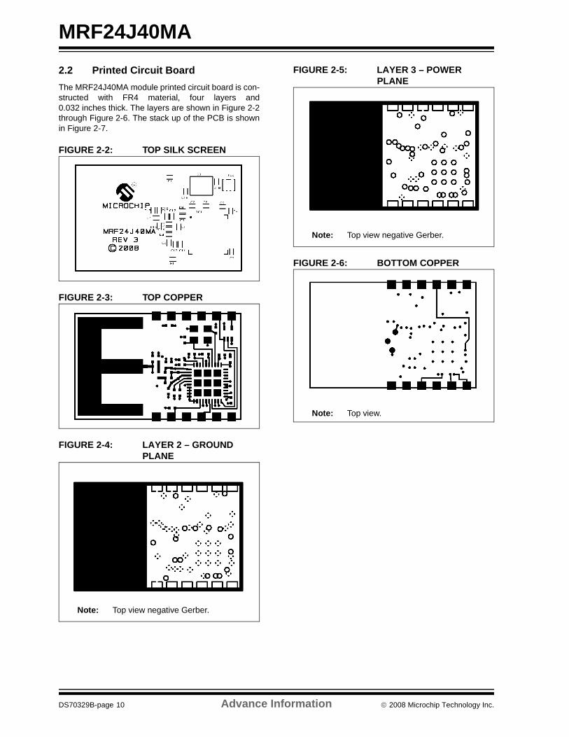
2.2 Printed Circuit BoardThe MRF24J40MA module printed circuit board is con-structed with FR4 material, four layers and0.032 inches thick. The layers are shown in Figure 2-2through Figure 2-6. The stack up of the PCB is shownin Figure 2-7.FIGURE 2-2: TOP SILK SCREEN
FIGURE 2-3: TOP COPPER
FIGURE 2-4: LAYER 2 – GROUND PLANE
FIGURE 2-5: LAYER 3 – POWER PLANE
FIGURE 2-6: BOTTOM COPPER
Note: Top view negative Gerber.
Note: Top view negative Gerber.
Note: Top view.
DS70329B-page 10 Advance Information © 2008 Microchip Technology Inc.

MRF24J40MA
FIGURE 2-7: PCB LAYER STACK UPTop Copper
Ground Plane
Power Plane
Bottom Copper
1/2 oz. Copper
1/2 oz. Copper
1/2 oz. Copper
1/2 oz. Copper
8 mil FR4
12 mil FR4
8 mil FR4
0.032”
+/- 0.005”
© 2008 Microchip Technology Inc. Advance Information DS70329B-page 11

MRF24J40MA
2.3 PCB AntennaThe PCB antenna is fabricated on the top copper trace.Figure 2-8 shows the trace dimensions. The layersbelow the antenna have no copper traces. The groundand power planes under the components serve as acounterpoise to the PCB antenna. Additional groundplane on the host PCB will substantially enhance theperformance of the module. For best performance,place the module on the host PCB following therecommendations in Section 1.2 “Mounting Details”.The Printed Circuit Board (PCB) antenna was designedand simulated using Ansoft Designer® and HFSS™ 3Dfull-wave solver software by Ansoft Corporation(www.ansoft.com). The design goal was to create acompact, low-cost antenna with the best radiationpattern. Figure 2-9 shows the simulation drawing andFigure 2-10 and Figure 2-11 show the 2D and 3Dradiation patterns, respectively. As shown by theradiation patterns, the performance of the antenna isdependant upon the orientation of the module.Figure 2-12 shows the impedance simulation andFigure 2-13 shows the actual impedance measurement.The discrete matching circuitry matches the impedanceof the antenna with the MRF24J40 transceiver IC.
FIGURE 2-8: PCB ANTENNA DIMENSIONS
FIGURE 2-9: PCB ANTENNA SIMULATION DRAWING
4.0 mm
16.5 mm
11.0 mm
2.5 mm2.0 mm5.0 mm
X
Y
Z
DS70329B-page 12 Advance Information © 2008 Microchip Technology Inc.

MRF24J40MA
FIGURE 2-10: SIMULATED 2D RADIATION PATTERNFIGURE 2-11: SIMULATED 3D RADIATION PATTERN
dB (Gain Total) 2.0921e+000 1.1359e-001-1.8649e+000-3.8435e+000-5.8220e+000-7.8005e+000 -9.7791e+000-1.1758e-001-1.3736e+001-1.5715e+001-1.7693e+001-1.9672e+001-2.1650e+001-2.3629e-001-2.5607e+001-2.7586e+001-2.9564e+001
Theta
Phi
Z
Y
X
© 2008 Microchip Technology Inc. Advance Information DS70329B-page 13

MRF24J40MA
FIGURE 2-12: SIMULATED PCB ANTENNA IMPEDANCEFIGURE 2-13: MEASURED PCB ANTENNA IMPEDANCE
DS70329B-page 14 Advance Information © 2008 Microchip Technology Inc.
MRF24J40MA
3.0 REGULATORY APPROVALThe MRF24J40MA module has received regulatoryapprovals for modular devices in the United States,Canada and European countries. Modular approvalallows the end user to place the MRF24J40MA moduleinside a finished product and not require regulatorytesting for an intentional radiator (RF transmitter), pro-vided no changes or modifications are made to themodule circuitry. Changes or modifications could voidthe user’s authority to operate the equipment. The enduser must comply with all of the instructions providedby the Grantee, which indicate installation and/oroperating conditions necessary for compliance.
The integrator may still be responsible for testing the endproduct for any additional compliance requirementsrequired with this module installed (for example: digitaldevice emission, PC peripheral requirements, etc.) inthe specific country that the end device will be marketed.
Annex F of the IEEE Std. 802.15.4 document has a goodsummary of regulatory requirements in various countriesconcerning IEEE Std. 802.15.4 devices. The standardcan be downloaded from the IEEE Standards web page:http://standards.ieee.org/getieee802/802.15.html.
Refer to the specific country radio regulations fordetails on regulatory compliance.
3.1 United StatesThe MRF24J40MA has received Federal Communica-tions Commission (FCC) CFR47 Telecommunications,Part 15 Subpart C “Intentional Radiators” 15.247 andmodular approval in accordance with FCC PublicNotice DA 00-1407 Released: June 26, 2000, Part 15Unlicensed Modular Transmitter Approval. TheMRF24J40MA module can be integrated into a finishedproduct without obtaining subsequent and separateFCC approvals.
The MRF24J40MA module has been labeled with itsown FCC ID number, and if the FCC ID is not visiblewhen the module is installed inside another device,then the outside of the finished product into which themodule is installed must also display a label referring tothe enclosed module. This exterior label can usewording such as the following:
The user’s manual should include the followingstatement:
3.1.1 RF EXPOSUREAll transmitters regulated by FCC must comply with RFexposure requirements. OET Bulletin 65 “EvaluatingCompliance with FCC Guidelines for Human Exposureto Radio Frequency Electromagnetic Fields” providesassistance in determining whether proposed or existingtransmitting facilities, operations or devices complywith limits for human exposure to Radio Frequency(RF) fields adopted by the Federal CommunicationsCommission (FCC). The bulletin offers guidelines andsuggestions for evaluating compliance.
If appropriate, compliance with exposure guidelines formobile and unlicensed devices can be accomplishedby the use of warning labels and by providing userswith information concerning minimum separationdistances from transmitting structures and properinstallation of antennas.
Contains Transmitter Module FCC ID: OA3MRF24J40MA
-or-
Contains FCC ID: OA3MRF24J40MA
This device complies with Part 15 of the FCC Rules.Operation is subject to the following two conditions:(1) this device may not cause harmful interference,and (2) this device must accept any interferencereceived, including interference that may causeundesired operation.
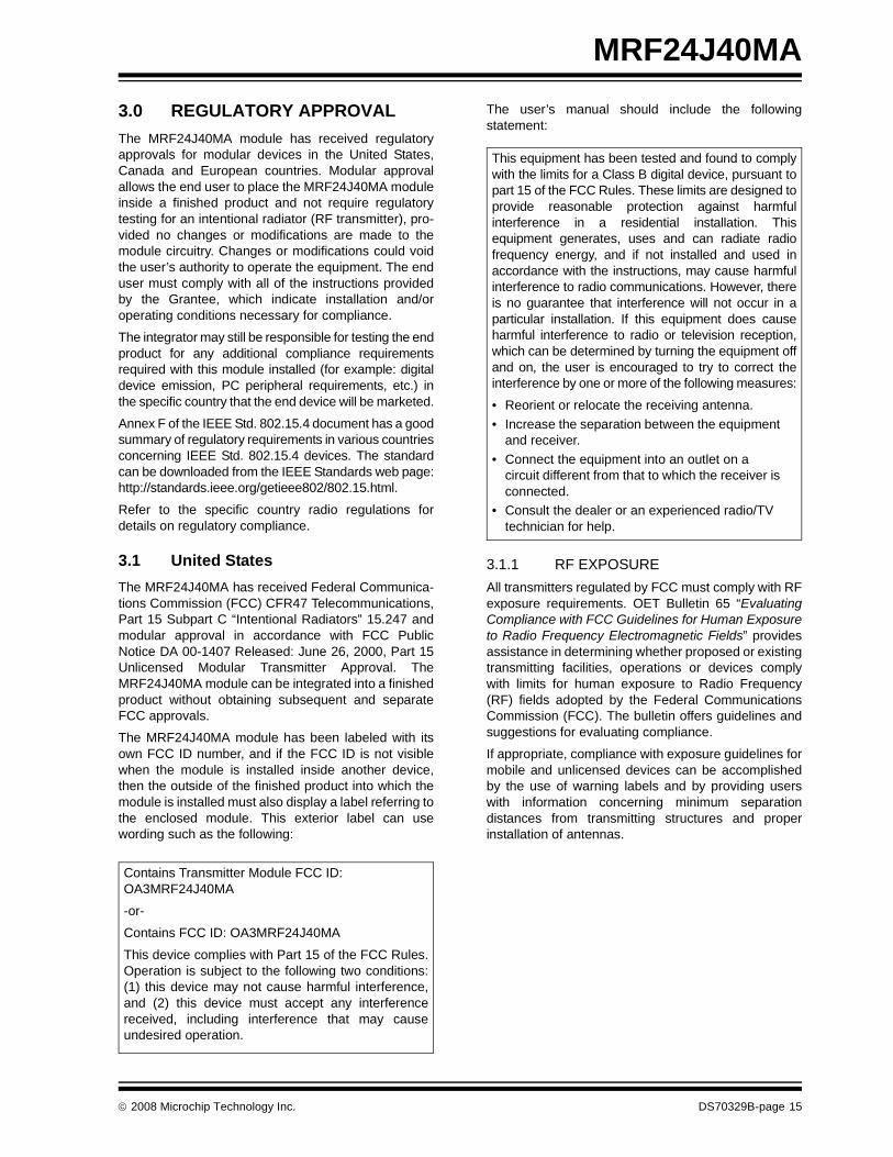
This equipment has been tested and found to complywith the limits for a Class B digital device, pursuant topart 15 of the FCC Rules. These limits are designed toprovide reasonable protection against harmfulinterference in a residential installation. Thisequipment generates, uses and can radiate radiofrequency energy, and if not installed and used inaccordance with the instructions, may cause harmfulinterference to radio communications. However, thereis no guarantee that interference will not occur in aparticular installation. If this equipment does causeharmful interference to radio or television reception,which can be determined by turning the equipment offand on, the user is encouraged to try to correct theinterference by one or more of the following measures:
• Reorient or relocate the receiving antenna.• Increase the separation between the equipment
and receiver.• Connect the equipment into an outlet on a
circuit different from that to which the receiver is connected.
• Consult the dealer or an experienced radio/TV technician for help.
© 2008 Microchip Technology Inc. DS70329B-page 15

MRF24J40MA
The following statement must be included as aCAUTION statement in manuals and OEM products toalert users of FCC RF Exposure compliance:If the MRF24J40MA module is used in a portableapplication (antenna is less than 20 cm from personsduring operation), the integrator is responsible forperforming Specific Absorption Rate (SAR) testing inaccordance with FCC rules 2.1091.
3.1.2 HELPFUL WEB SITESFederal Communications Commission (FCC):http://www.fcc.gov
3.2 CanadaThe MRF24J40MA module has been certified for use inCanada under Industry Canada (IC) Radio StandardsSpecification (RSS) RSS-210 and RSS-Gen.
From Section 7.1.1, RSS-Gen, Issue 2, June 2007,Modular Transmitter Approval:
Host devices which contain separately certifiedmodules do not need to be recertified, provided thatthey meet the following conditions:
a) The host device, as a stand-alone unitwithout any separately certified modules,complies with all applicable Radio StandardsSpecifications.
b) The host device and all the separatelycertified modules it contains jointly meet theRF exposure compliance requirements ofRSS-102, if applicable.
c) The host device complies with thecertification labeling requirements of each ofthe modules it contains.
From Section 5.2, RSS-Gen, Issue 2, June 2007,Equipment Labels:
All Category I radio equipment intended for use inCanada shall permanently display on each transmitter,receiver or inseparable combination thereof, theapplicant’s name (i.e., manufacturer’s name, tradename or brand name), model number and certificationnumber. This information shall be affixed in such amanner as to not be removable except by destruction ordefacement. The size of the lettering shall be legiblewithout the aid of magnification, but is not required to belarger than 8-point font size. If the device is too small tomeet this condition, the information can be included inthe user manual upon agreement with Industry Canada.
Label:
From Section 7.1.6, RSS-Gen, Issue 2, June 2007,Digital Circuits:
If the device contains digital circuitry that is not directlyassociated with the radio transmitter, the device shallalso have to comply with ICES-003, Class A or B asappropriate, except for ICES-003 labelingrequirements. The test data obtained (for the ICES-003tests) shall be kept by the manufacturer or importerwhose name appears on the equipment label, andmade available to Industry Canada on request, for aslong as the model is being marketed in Canada.
3.2.1 HELPFUL WEB SITESIndustry Canada: http://www.ic.gc.ca/
Note: Compliance of a module in its finalconfiguration is the responsibility of theapplicant. A host device will not beconsidered certified if the instructionsregarding antenna configuration providedin the original description, of one or moreseparately certified modules it contains,were not followed
To satisfy FCC RF Exposure requirements for mobileand base station transmission devices, a separationdistance of 20 cm or more should be maintainedbetween the antenna of this device and personsduring operation. To ensure compliance, operation atcloser than this distance is not recommended.
The antenna(s) used for this transmitter must not beco-located or operating in conjunction with any otherantenna or transmitter.
Contains IC: 7693A-24J40MA
DS70329B-page 16 © 2008 Microchip Technology Inc.

MRF24J40MA
3.3 EuropeThe MRF24J40MA module has been certified for use inEuropean countries. The following testing has beencompleted:Test standard ETSI EN 300 328 V1.7.1 (2006-10):
• Maximum Transmit Power• Maximum EIRP Spectral Density• Frequency Range• Radiated Emissions
Test standards ETSI EN 301 489-1:2008 and ETSIEN 301 489-17:2008:
• Radiated Emissions• Electro-Static Discharge• Radiated RF Susceptibility
A helpful document that can be used as a starting pointin understanding the use of Short Range Devices (SRD)in Europe is the European Radio Communications Com-mittee (ERC) Recommendation 70-03 E, downloadablefrom the European Radio Communications Office(ERO): http://www.ero.dk.
The end user is responsible for ensuring compliancewith harmonized frequencies and labelingrequirements for each country the end device ismarketed and sold.
3.3.1 HELPFUL WEB SITES:Radio and Telecommunications Terminal Equipment(R&TTE):http://ec.europa.eu/enterprise/rtte/index_en.htm
European Conference of Postal and TelecommunicationsAdministrations (CEPT): http://www.cept.org/
European Telecommunications Standards Institute(ETSI): http://www.etsi.org/
European Radio Communications Office (ERO):http://www.ero.dk/
© 2008 Microchip Technology Inc. DS70329B-page 17

MRF24J40MA
NOTES:DS70329B-page 18 © 2008 Microchip Technology Inc.

MRF24J40MA
4.0 ELECTRICAL CHARACTERISTICS
TABLE 4-1: RECOMMENDED OPERATING CONDITIONS
TABLE 4-2: CURRENT CONSUMPTION (TA = 25°C, VDD = 3.3V)
TABLE 4-3: RECEIVER AC CHARACTERISTICSTypical values are at TA = 25°C, VDD = 3.3V, LO Frequency = 2.445 GHz
Parameters Min Typ Max Units
Ambient Operating Temperature -40 — +85 °CSupply Voltage for RF, Analog and Digital Circuits
2.4 — 3.6 V
Supply Voltage for Digital I/O 2.4 3.3 3.6 VInput High Voltage (VIH) 0.5 x VDD — VDD + 0.3 VInput Low Voltage (VIL) -0.3 — 0.2 x VDD V
Chip Mode Condition Min Typ Max Units
Sleep Sleep Clock Disabled — 2 — μATX At Maximum Output Power — 23 — mARX — 19 — mA
Parameters Condition Min Typ Max Units
RF Input Frequency Compatible to IEEE Std. 802.15.4™, 2003
2.405 — 2.480 GHz
RF Sensitivity — -94 — dBmMaximum RF Input +5 — — dBmLO Leakage Measured at Balun Matching
Network Input at Frequency, 2.405-2.48 GHz
— -60 — dBm
Input Return Loss Externally Matched to 50 ohm Source by a Balun Matching Network
-8 -12 — dB
Noise Figure(including matching)
— 8 — dB
Adjacent Channel Rejection
@ +/-5 MHz 30 — — dB
Alternate Channel Rejection
@ +/-10 MHz 40 — — dB
RSSI Range — 50 — dBRSSI Error -5 — 5 dB
© 2008 Microchip Technology Inc. DS70329B-page 19

MRF24J40MA
TABLE 4-4: TRANSMITTER AC CHARACTERISTICSTypical values are at TA = 25°C, VDD = 3.3V, LO Frequency = 2.445 GHzParameters Condition Min Typ Max Units
RF Carrier Frequency 2.405 — 2.480 GHzMaximum RF Output Power
— 0 — dBm
RF Output Power Control Range
— 36 — dB
TX Gain Control Resolution
Programmed by Register — 1.25 — dB
Carrier Suppression — -30 — dBcTX Spectrum Mask for O-QPSK Signal
Offset Frequency > 3.5 MHz, at 0 dBm Output Power
-33 — — dBm
TX EVM — 15 — %
DS70329B-page 20 © 2008 Microchip Technology Inc.
MRF24J40MA
APPENDIX A: REVISION HISTORY
Revision A (June 2008)Original data sheet for the MRF24J40MA device.
Revision B (November 2008)Changed C17 to 1.0 pF and removed CLKOUT signal.
© 2008 Microchip Technology Inc. DS70329B-page 21

MRF24J40MA
NOTES:DS70329B-page 22 © 2008 Microchip Technology Inc.

DS70329B-page 23 © 2008 Microchip Technology Inc.
MRF24J40MA
INDEXAAC Characteristics
Receiver ......................................................................19Transmitter ..................................................................20
Antenna ImpedanceMeasured PCB............................................................14Simulated PCB............................................................14
BBlock Diagrams
Microcontroller to MRF24J40MA Interface....................4MRF24J40MA ...............................................................3
CCircuit Description .................................................................7Customer Change Notification Service ...............................24Customer Notification Service .............................................24Customer Notification System...............................................2Customer Support ...............................................................24
EElectrical Characteristics .....................................................19
Current Consumption ..................................................19Recommended Operating Conditions .........................19
Errata.....................................................................................2European Radio Communications (ERC)............................17
FFCC ID Number...................................................................15FCC RF Exposure Compliance ...........................................16
HHelpful Web Sites..........................................................16, 17
IInterface Description .............................................................3Internet Address ..................................................................24
MMAC/Baseband Features ......................................................1Microchip Internet Web Site ................................................24MiWi P2P...............................................................................3MiWi Protocol ........................................................................3More Information ...................................................................2
Customer Notification System.......................................2Errata ............................................................................2
Mounting Details....................................................................5MRF24J40 Data Sheet......................................................3, 7MRF24J40MA Bill of Materials (BOM) ..................................9MRF24J40MA Schematic......................................................8
OOverview ............................................................................... 3
PPCB Antenna ...................................................................... 12
Dimensions ................................................................. 12Simulation Drawing..................................................... 12
PCB LayersBottom Copper............................................................ 10Layer 2 – Ground Plane.............................................. 10Layer 3 – Power Plane ............................................... 10Stack Up ..................................................................... 11Top Copper................................................................. 10Top Silk Screen .......................................................... 10
Pin Description...................................................................... 4Pin Diagram .......................................................................... 1Printed Circuit Board (PCB) ................................................ 10
RRadiation Pattern
2D ............................................................................... 133D ............................................................................... 13
Reader Response ............................................................... 25Regulatory Approval ........................................................... 15
Canada ....................................................................... 16Europe ........................................................................ 17United States .............................................................. 15
Revision History .................................................................. 21RF Exposure ....................................................................... 15RF/Analog Features.............................................................. 1
SSerial I/O
SCK, SDI, SDO, CS...................................................... 7Short Range Devices (SRD) ............................................... 17Specific Absorption Rate (SAR).......................................... 16SPI ........................................................................................ 7
WWWW Address.................................................................... 24WWW, On-Line Support ....................................................... 2
ZZigBee Protocol .................................................................... 3

MRF24J40MA
DS70329B-page 24 © 2008 Microchip Technology Inc.
NOTES:

MRF24J40MA
THE MICROCHIP WEB SITEMicrochip provides online support via our WWW site atwww.microchip.com. This web site is used as a meansto make files and information easily available tocustomers. Accessible by using your favorite Internetbrowser, the web site contains the followinginformation:
• Product Support – Data sheets and errata, application notes and sample programs, design resources, user’s guides and hardware support documents, latest software releases and archived software
• General Technical Support – Frequently Asked Questions (FAQ), technical support requests, online discussion groups, Microchip consultant program member listing
• Business of Microchip – Product selector and ordering guides, latest Microchip press releases, listing of seminars and events, listings of Microchip sales offices, distributors and factory representatives
CUSTOMER CHANGE NOTIFICATION SERVICEMicrochip’s customer notification service helps keepcustomers current on Microchip products. Subscriberswill receive e-mail notification whenever there arechanges, updates, revisions or errata related to aspecified product family or development tool of interest.
To register, access the Microchip web site atwww.microchip.com, click on Customer ChangeNotification and follow the registration instructions.
CUSTOMER SUPPORTUsers of Microchip products can receive assistancethrough several channels:
• Distributor or Representative• Local Sales Office• Field Application Engineer (FAE)• Technical Support• Development Systems Information Line
Customers should contact their distributor,representative or field application engineer (FAE) forsupport. Local sales offices are also available to helpcustomers. A listing of sales offices and locations isincluded in the back of this document.
Technical support is available through the web siteat: http://support.microchip.com
© 2008 Microchip Technology Inc. DS70329B-page 25

MRF24J40MA
READER RESPONSEIt is our intention to provide you with the best documentation possible to ensure successful use of your Microchip prod-uct. If you wish to provide your comments on organization, clarity, subject matter, and ways in which our documentationcan better serve you, please FAX your comments to the Technical Publications Manager at (480) 792-4150.
Please list the following information, and use this outline to provide us with your comments about this document.
To: Technical Publications Manager
RE: Reader ResponseTotal Pages Sent ________
From: Name
CompanyAddressCity / State / ZIP / Country
Telephone: (_______) _________ - _________
Application (optional):
Would you like a reply? Y N
Device: Literature Number:
Questions:
FAX: (______) _________ - _________
DS70329BMRF24J40MA
1. What are the best features of this document?
2. How does this document meet your hardware and software development needs?
3. Do you find the organization of this document easy to follow? If not, why?
4. What additions to the document do you think would enhance the structure and subject?
5. What deletions from the document could be made without affecting the overall usefulness?
6. Is there any incorrect or misleading information (what and where)?
7. How would you improve this document?
DS70329B-page 26 © 2008 Microchip Technology Inc.
© 2008 Microchip Technology Inc. DS70329B-page 27
MRF24J40MA
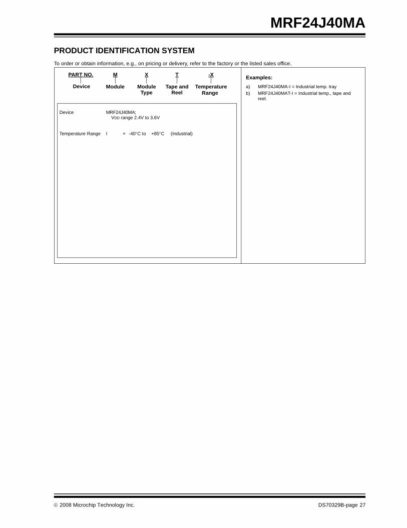
PRODUCT IDENTIFICATION SYSTEMTo order or obtain information, e.g., on pricing or delivery, refer to the factory or the listed sales office.
PART NO. -XX T
Tape andModule TemperatureRange
Device
Device MRF24J40MA;
VDD range 2.4V to 3.6V
Temperature Range I = -40°C to +85°C (Industrial)
Examples:a) MRF24J40MA-I = Industrial temp. trayb) MRF24J40MAT-I = Industrial temp., tape and
reel.
M
ModuleType Reel

DS70329B-page 28 © 2008 Microchip Technology Inc.
AMERICASCorporate Office2355 West Chandler Blvd.Chandler, AZ 85224-6199Tel: 480-792-7200 Fax: 480-792-7277Technical Support: http://support.microchip.comWeb Address: www.microchip.comAtlantaDuluth, GA Tel: 678-957-9614 Fax: 678-957-1455BostonWestborough, MA Tel: 774-760-0087 Fax: 774-760-0088ChicagoItasca, IL Tel: 630-285-0071 Fax: 630-285-0075DallasAddison, TX Tel: 972-818-7423 Fax: 972-818-2924DetroitFarmington Hills, MI Tel: 248-538-2250Fax: 248-538-2260KokomoKokomo, IN Tel: 765-864-8360Fax: 765-864-8387Los AngelesMission Viejo, CA Tel: 949-462-9523 Fax: 949-462-9608Santa ClaraSanta Clara, CA Tel: 408-961-6444Fax: 408-961-6445TorontoMississauga, Ontario, CanadaTel: 905-673-0699 Fax: 905-673-6509
ASIA/PACIFICAsia Pacific OfficeSuites 3707-14, 37th FloorTower 6, The GatewayHarbour City, KowloonHong KongTel: 852-2401-1200Fax: 852-2401-3431Australia - SydneyTel: 61-2-9868-6733Fax: 61-2-9868-6755China - BeijingTel: 86-10-8528-2100 Fax: 86-10-8528-2104China - ChengduTel: 86-28-8665-5511Fax: 86-28-8665-7889China - Hong Kong SARTel: 852-2401-1200 Fax: 852-2401-3431China - NanjingTel: 86-25-8473-2460Fax: 86-25-8473-2470China - QingdaoTel: 86-532-8502-7355Fax: 86-532-8502-7205China - ShanghaiTel: 86-21-5407-5533 Fax: 86-21-5407-5066China - ShenyangTel: 86-24-2334-2829Fax: 86-24-2334-2393China - ShenzhenTel: 86-755-8203-2660 Fax: 86-755-8203-1760China - WuhanTel: 86-27-5980-5300Fax: 86-27-5980-5118China - XiamenTel: 86-592-2388138 Fax: 86-592-2388130China - XianTel: 86-29-8833-7252Fax: 86-29-8833-7256China - ZhuhaiTel: 86-756-3210040 Fax: 86-756-3210049
ASIA/PACIFICIndia - BangaloreTel: 91-80-4182-8400 Fax: 91-80-4182-8422India - New DelhiTel: 91-11-4160-8631Fax: 91-11-4160-8632India - PuneTel: 91-20-2566-1512Fax: 91-20-2566-1513Japan - YokohamaTel: 81-45-471- 6166 Fax: 81-45-471-6122Korea - DaeguTel: 82-53-744-4301Fax: 82-53-744-4302Korea - SeoulTel: 82-2-554-7200Fax: 82-2-558-5932 or 82-2-558-5934Malaysia - Kuala LumpurTel: 60-3-6201-9857Fax: 60-3-6201-9859Malaysia - PenangTel: 60-4-227-8870Fax: 60-4-227-4068Philippines - ManilaTel: 63-2-634-9065Fax: 63-2-634-9069SingaporeTel: 65-6334-8870Fax: 65-6334-8850Taiwan - Hsin ChuTel: 886-3-572-9526Fax: 886-3-572-6459Taiwan - KaohsiungTel: 886-7-536-4818Fax: 886-7-536-4803Taiwan - TaipeiTel: 886-2-2500-6610 Fax: 886-2-2508-0102Thailand - BangkokTel: 66-2-694-1351Fax: 66-2-694-1350
EUROPEAustria - WelsTel: 43-7242-2244-39Fax: 43-7242-2244-393Denmark - CopenhagenTel: 45-4450-2828 Fax: 45-4485-2829France - ParisTel: 33-1-69-53-63-20 Fax: 33-1-69-30-90-79Germany - MunichTel: 49-89-627-144-0 Fax: 49-89-627-144-44Italy - Milan Tel: 39-0331-742611 Fax: 39-0331-466781Netherlands - DrunenTel: 31-416-690399 Fax: 31-416-690340Spain - MadridTel: 34-91-708-08-90Fax: 34-91-708-08-91UK - WokinghamTel: 44-118-921-5869Fax: 44-118-921-5820
WORLDWIDE SALES AND SERVICE
01/02/08