mpq45 72 high -effic iency, 2a, 60 v , fully integrated
TRANSCRIPT

MPQ4572 High-Efficiency, 2A, 60V, Fully Integrated, Synchronous Buck Converter, AEC-Q100 Qualified
MPQ4572 Rev. 1.0 www.MonolithicPower.com 1
1/21/2020 MPS Proprietary Information. Patent Protected. Unauthorized Photocopy and Duplication Prohibited. © 2020 MPS. All Rights Reserved.
DESCRIPTION The MPQ4572 is a fully integrated, fixed-frequency, synchronous step-down converter. It can achieve up to 2A of continuous output current with peak current control for excellent transient response.
The wide 4.5V to 60V input voltage range accommodates a variety of step-down applications in an automotive input environment. The device’s 2μA shutdown mode quiescent current makes it ideal for battery-powered applications.
The MPQ4572 integrates internal high-side and low-side power MOSFETs for high efficiency without an external Schottky diode. It employs advanced asynchronous modulation (AAM) to achieve high efficiency during light-load conditions by scaling down the frequency to reduce switching and gate driver losses.
Standard features include built-in soft start, enable control, and power good indication. High-duty cycle and low-dropout mode are provided for automotive cold crank conditions.
The chip provides over-current protection (OCP) with valley-current detection to avoid current runaway. It also has hiccup short-circuit protection (SCP), input under-voltage lockout (UVLO), and auto-recovery thermal protection.
With internal compensation, the MPQ4572 can offer a very compact solution with a minimal number of readily available, standard external components. It is available in a QFN-12 (2.5mmx3mm) package.
FEATURES Wide 4.5V to 60V Operating Input Range
2A Continuous Output Current
High-Efficiency, Synchronous Mode Control
250mΩ/45mΩ Internal Power MOSFETs
Configurable Frequency Up to 2.2MHz
180° Out-of-Phase SYNC Out Clock
40μA Quiescent Current
Low Shutdown Mode Current: 2μA
FB-Tolerance: 1% at Room Temp, 2% at Full Temp
Selectable AAM or Forced CCM Operation during Light-Load Conditions
Internal 0.45ms Soft Start
Remote EN Control
Power Good Indicator
Low-Dropout Mode
Over-Current Protection (OCP)
Short-Circuit Protection with Hiccup Mode
VIN Under-Voltage Lockout (UVLO)
Thermal Shutdown
Available in a QFN-12 (2.5mmx3mm) Package
Available in a Wettable Flank Package
Available in AEC-Q100 Grade-1
APPLICATIONS
Automotive Infotainment
Automotive Lamps and LEDs
Automotive Motor Control
Industrial Power Systems
All MPS parts are lead-free, halogen-free, and adhere to the RoHS directive. For MPS green status, please visit the MPS website under Quality Assurance. “MPS”, the MPS logo, and “Simple, Easy Solutions” are trademarks of Monolithic Power Systems, Inc. or its subsidiaries.

MPQ4572 – 60V, 2A, SYNCHRONOUS STEP-DOWN CONVERTER, AEC-Q100
MPQ4572 Rev. 1.0 www.MonolithicPower.com 2
1/21/2020 MPS Proprietary Information. Patent Protected. Unauthorized Photocopy and Duplication Prohibited. © 2020 MPS. All Rights Reserved.
TYPICAL APPLICATION
FREQ
IN
VCC
4.5V to 60VBST
SW
MPQ4572
ENEN
VIN
VOUTGND
FB
GND
GND
CCM/SYNCOPG PG
Efficiency vs. Load Current VOUT = 5V, L = 15μH, fSW = 400kHz, AAM
0.00
0.20
0.40
0.60
0.80
1.00
1.20
1.40
1.60
20
30
40
50
60
70
80
90
100
1 10 100 1000
PO
WE
R L
OS
S (
W)
EFFIC
IEN
CY
(%
)
LOAD CURRENT (mA)
VIN=8VVIN=12VVIN=24VVIN=36VVin=48VVIN=60V

MPQ4572 – 60V, 2A, SYNCHRONOUS STEP-DOWN CONVERTER, AEC-Q100
MPQ4572 Rev. 1.0 www.MonolithicPower.com 3
1/21/2020 MPS Proprietary Information. Patent Protected. Unauthorized Photocopy and Duplication Prohibited. © 2020 MPS. All Rights Reserved.
ORDERING INFORMATION Part Number* Package Top Marking MSL Rating**
MPQ4572GQB
QFN-12 (2.5mmx3mm) See Below 1 MPQ4572GQB-AEC1
MPQ4572GQBE-AEC1***
* For Tape & Reel, add suffix –Z (e.g. MPQ4572GQB–Z). ** Moisture Sensitivity Level Rating.
*** Wettable flank.
TOP MARKING (MPQ4572GQB AND MPQ4572GQB-AEC1)
AVN: Product code of MPQ4572GQB and MPQ4572GQB-AEC1 Y: Year code WW: Week code LLL: Lot number
TOP MARKING (MPQ4572GQBE-AEC1)
BMM: Product code of MPQ4572GQBE-AEC1 Y: Year code WW: Week code LLL: Lot number
MPQ4572 – 60V, 2A, SYNCHRONOUS STEP-DOWN CONVERTER, AEC-Q100
MPQ4572 Rev. 1.0 www.MonolithicPower.com 4
1/21/2020 MPS Proprietary Information. Patent Protected. Unauthorized Photocopy and Duplication Prohibited. © 2020 MPS. All Rights Reserved.
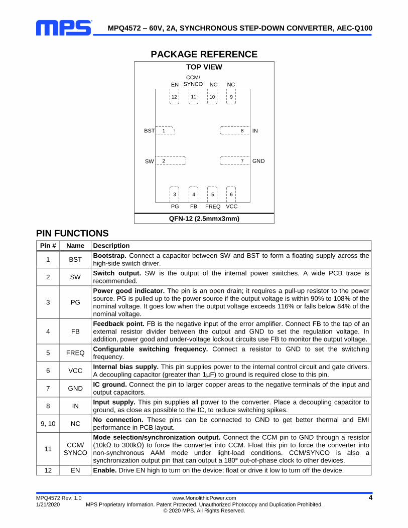
PACKAGE REFERENCE
TOP VIEW
1
2
3 4 5 6
7
8
FB VCC
EN
BST
SW
IN
GND
9101112
PG FREQ
NCNC
CCM/
SYNCO
QFN-12 (2.5mmx3mm)
PIN FUNCTIONS
Pin # Name Description
1 BST Bootstrap. Connect a capacitor between SW and BST to form a floating supply across the high-side switch driver.
2 SW Switch output. SW is the output of the internal power switches. A wide PCB trace is recommended.
3 PG
Power good indicator. The pin is an open drain; it requires a pull-up resistor to the power source. PG is pulled up to the power source if the output voltage is within 90% to 108% of the nominal voltage. It goes low when the output voltage exceeds 116% or falls below 84% of the nominal voltage.
4 FB Feedback point. FB is the negative input of the error amplifier. Connect FB to the tap of an external resistor divider between the output and GND to set the regulation voltage. In addition, power good and under-voltage lockout circuits use FB to monitor the output voltage.
5 FREQ Configurable switching frequency. Connect a resistor to GND to set the switching frequency.
6 VCC Internal bias supply. This pin supplies power to the internal control circuit and gate drivers. A decoupling capacitor (greater than 1µF) to ground is required close to this pin.
7 GND IC ground. Connect the pin to larger copper areas to the negative terminals of the input and output capacitors.
8 IN Input supply. This pin supplies all power to the converter. Place a decoupling capacitor to ground, as close as possible to the IC, to reduce switching spikes.
9, 10 NC No connection. These pins can be connected to GND to get better thermal and EMI performance in PCB layout.
11 CCM/
SYNCO
Mode selection/synchronization output. Connect the CCM pin to GND through a resistor (10kΩ to 300kΩ) to force the converter into CCM. Float this pin to force the converter into non-synchronous AAM mode under light-load conditions. CCM/SYNCO is also a synchronization output pin that can output a 180° out-of-phase clock to other devices.
12 EN Enable. Drive EN high to turn on the device; float or drive it low to turn off the device.

MPQ4572 – 60V, 2A, SYNCHRONOUS STEP-DOWN CONVERTER, AEC-Q100
MPQ4572 Rev. 1.0 www.MonolithicPower.com 5
1/21/2020 MPS Proprietary Information. Patent Protected. Unauthorized Photocopy and Duplication Prohibited. © 2020 MPS. All Rights Reserved.
ABSOLUTE MAXIMUM RATINGS (1) VIN .............................................................. 65V VSW ....................................... -0.3V to VIN + 0.3V VBST .....................................................VSW + 6V All other pins .................................. -0.3V to +6V Continuous power dissipation (TA = 25°C) (2) QFN-12 (2.5mmx3mm) ............................ 2.08W Junction temperature ............................... 150°C Lead temperature .................................... 260°C Storage temperature ................ -65°C to +150°C
Electrostatic Discharge (ESD) Rating
HBM (Human body model) ........................ ±2kV
CDM (Charged device model) ................. ±750V
Recommended Operating Conditions
Continuous supply voltage (VIN) ...... 4.5V to 60V Output voltage (VOUT) ............... 1V to 90% of VIN Load current range .............................. 0A to 2A Operating junction temp (TJ) .... -40°C to +150°C
Thermal Resistance θJA θJC
QFN-12 (2.5mmx3mm)
JESD51-7 (3).............................60......13....°C/W EVQ4572-QB-00A (4)................45......11....°C/W
Notes:
1) Absolute maximum ratings are rated under room temperature, unless otherwise noted. Exceeding these ratings may damage the device.
2) The maximum allowable power dissipation is a function of the maximum junction temperature TJ (MAX), the junction-to-ambient thermal resistance θJA, and the ambient temperature TA. The maximum allowable continuous power dissipation at any ambient temperature is calculated by PD (MAX) = (TJ
(MAX) - TA) / θJA. Exceeding the maximum allowable power dissipation will cause excessive die temperature, and the module will go into thermal shutdown. Internal thermal shutdown circuitry protects the device from permanent damage.
3) Measured on JESD51-7, 4-layer PCB. 4) Measured on MPS standard EVB: 8.9cmx8.9cm, 2oz copper
thick, 4-layer PCB.
MPQ4572 – 60V, 2A, SYNCHRONOUS STEP-DOWN CONVERTER, AEC-Q100
MPQ4572 Rev. 1.0 www.MonolithicPower.com 6
1/21/2020 MPS Proprietary Information. Patent Protected. Unauthorized Photocopy and Duplication Prohibited. © 2020 MPS. All Rights Reserved.
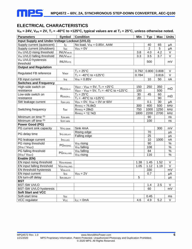
ELECTRICAL CHARACTERISTICS VIN = 24V, VEN = 2V, TJ = -40°C to +125°C, typical values are at TJ = 25°C, unless otherwise noted.
Parameters Symbol Condition Min Typ Max Units
Input Supply and Under-Voltage Lockout (UVLO)
Supply current (quiescent) IQ No load, VFB = 0.85V, AAM 40 65 μA
Supply current (shutdown) ISD VEN = 0V 2 5 μA
VIN UVLO rising threshold INUVVth-R 3.8 4.0 4.2 V
VIN UVLO falling threshold INUVVth-F 3.3 3.5 3.7 V
VIN UVLO hysteresis threshold
INUVHYS 500 mV
Output and Regulation
Regulated FB reference VREF TJ = 25°C 0.792 0.800 0.808 V
TJ = -40°C to +125°C 0.784 0.816 V
FB input current IFB VFB = 0.85V 10 50 nA
Switches and Frequency
High-side switch on resistance
RDSON-H VBST - VSW = 5V, TJ = +25°C 150 250 350
mΩ VBST - VSW = 5V, TJ = -40°C to +125°C 100 500
Low-side switch on resistance
RDSON-L TJ = 25°C 30 45 60
mΩ TJ = -40°C to +125°C 20 90
SW leakage current ISW-LKG VEN = 0V, VSW = 0V or 60V 0.1 30 μA
Switching frequency fSW
RFREQ = 76.8kΩ 300 400 500 kHz
RFREQ = 28kΩ 750 1000 1250 kHz
RFREQ = 12.1kΩ 1800 2200 2700 kHz
Minimum on time (5) tON-MIN 90 ns
Minimum off time (5) tOFF-MIN 100 ns
Power Good (PG)
PG current sink capacity VPG-SINK Sink 4mA 300 mV
PG delay time tPG-DELAY Rising edge 70 μs
Falling edge 25 μs
PG leakage current IPG-LKG 10 1000 nA
PG rising threshold (VFB / VREF)
PGRISING VFB rising 90 %
VFB falling 108 %
PG falling threshold (VFB / VREF)
PGFALLING VFB falling 84 %
VFB rising 116 %
Enable (EN)
EN input rising threshold VEN-RISING 1.38 1.45 1.52 V
EN input falling threshold VEN-FALLING 1.05 1.12 1.19 V
EN threshold hysteresis VEN-HYS 330 mV
EN input current IEN VEN = 2V 0.7 μA
EN turn-off delay tEN-DELAY 5 μs
BST
BST-SW UVLO 1.4 2.5 V
BST-SW UVLO hysteresis 60 mV
Soft Start and VCC
Soft-start time tSS 0.45 ms
VCC regulator VCC ICC = 0mA 4.6 4.9 5.2 V
MPQ4572 – 60V, 2A, SYNCHRONOUS STEP-DOWN CONVERTER, AEC-Q100
MPQ4572 Rev. 1.0 www.MonolithicPower.com 7
1/21/2020 MPS Proprietary Information. Patent Protected. Unauthorized Photocopy and Duplication Prohibited. © 2020 MPS. All Rights Reserved.
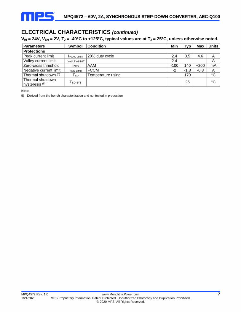
ELECTRICAL CHARACTERISTICS (continued) VIN = 24V, VEN = 2V, TJ = -40°C to +125°C, typical values are at TJ = 25°C, unless otherwise noted.
Parameters Symbol Condition Min Typ Max Units
Protections
Peak current limit IPEAK-LIMIT 20% duty cycle 2.4 3.5 4.6 A
Valley current limit IVALLEY-LIMIT 2.4 A
Zero-cross threshold IZCD AAM -100 140 +300 mA
Negative current limit INEG-LIMIT FCCM -2 -1.3 -0.8 A
Thermal shutdown (5) TSD Temperature rising 170 °C
Thermal shutdown hysteresis (5)
TSD-SYS 25 °C
Note:
5) Derived from the bench characterization and not tested in production.

MPQ4572 – 60V, 2A, SYNCHRONOUS STEP-DOWN CONVERTER, AEC-Q100
MPQ4572 Rev. 1.0 www.MonolithicPower.com 8
1/21/2020 MPS Proprietary Information. Patent Protected. Unauthorized Photocopy and Duplication Prohibited. © 2020 MPS. All Rights Reserved.
TYPICAL CHARACTERISTICS VIN = 24V, TJ = -40°C to +125°C, unless otherwise noted.
Quiescent Current vs. Temperature
Shutdown Current vs. Temperature
30
35
40
45
50
-50 -25 0 25 50 75 100 125
I Q(μ
A)
TEMPERATURE (oC)
1.8
1.9
2.0
2.1
2.2
2.3
2.4
2.5
-50 -25 0 25 50 75 100 125
I SH
UT
(μA
)
TEMPERATURE (oC)
VIN UVLO Threshold vs. Temperature
Feedback Reference vs. Temperature
3.4
3.5
3.6
3.7
3.8
3.9
4.0
4.1
-50 -25 0 25 50 75 100 125
VIN
UV
LO
TH
RE
SH
OL
D
(V)
TEMPERATURE (°C)
RisingFalling
0.790
0.795
0.800
0.805
0.810
-50 -25 0 25 50 75 100 125
VR
EF
(V)
TEMPERATURE (°C)
VCC vs. Temperature
EN Threshold vs. Temperature
4.86
4.88
4.90
4.92
4.94
-50 -25 0 25 50 75 100 125
VC
C(V
)
TEMPERATURE (°C)
1.0
1.1
1.2
1.3
1.4
1.5
-50 -25 0 25 50 75 100 125
VE
N(V
)
TEMPERATURE (°C)
RisingFalling

MPQ4572 – 60V, 2A, SYNCHRONOUS STEP-DOWN CONVERTER, AEC-Q100
MPQ4572 Rev. 1.0 www.MonolithicPower.com 9
1/21/2020 MPS Proprietary Information. Patent Protected. Unauthorized Photocopy and Duplication Prohibited. © 2020 MPS. All Rights Reserved.
TYPICAL CHARACTERISTICS (continued)
VIN = 24V, TJ = -40°C to +125°C, unless otherwise noted.
Zero-Current Detection (ZCD) vs. Temperature
Peak Current Limit vs. Temperature
110
120
130
140
150
160
-50 -25 0 25 50 75 100 125
I ZC
D(m
A)
TEMPERATURE (°C)
3.30
3.35
3.40
3.45
3.50
3.55
3.60
-50 -25 0 25 50 75 100 125
I LIM
IT(A
)TEMPERATURE (oC)
Valley Current Limit vs. Temperature
Negative Current Limit vs. Temperature
3.30
3.35
3.40
3.45
3.50
3.55
3.60
-50 -25 0 25 50 75 100 125
I LIM
IT-V
AL
LE
Y(A
)
TEMPERATURE (°C)
1.20
1.25
1.30
1.35
1.40
-50 -25 0 25 50 75 100 125
I LIM
IT-N
EG
AT
IVE
(A)
TEMPERATURE (oC)
HS-FET On Resistance vs. Temperature
LS-FET On Resistance vs. Temperature
200
250
300
350
400
-50 -25 0 25 50 75 100 125
RO
N-H
S(m
Ω)
TEMPERATURE (°C)
30
40
50
60
70
-50 -25 0 25 50 75 100 125
RO
N-L
S(m
Ω)
TEMPERATURE (°C)

MPQ4572 – 60V, 2A, SYNCHRONOUS STEP-DOWN CONVERTER
MPQ4572 Rev. 1.0 www.MonolithicPower.com 10
1/21/2020 MPS Proprietary Information. Patent Protected. Unauthorized Photocopy and Duplication Prohibited. © 2020 MPS. All Rights Reserved.
TYPICAL CHARACTERISTICS (continued)
VIN = 24V, TJ = -40°C to +125°C, unless otherwise noted.
PG Rising Threshold vs. Temperature
PG Falling Threshold vs. Temperature
85
90
95
100
105
110
115
-50 -25 0 25 50 75 100 125
PG
VT
H (A
S P
ER
CE
NT
AG
E
OF
VF
B)
TEMPERATURE (°C)
VFB FallingVFB Rising
80
85
90
95
100
105
110
115
120
-50 -25 0 25 50 75 100 125
PG
VT
H (A
S P
ER
CE
NT
AG
E
OF
VF
B)
TEMPERATURE (°C)
VFB RisingVFB Falling

MPQ4572 – 60V, 2A, SYNCHRONOUS STEP-DOWN CONVERTER, AEC-Q100
MPQ4572 Rev. 1.0 www.MonolithicPower.com 11
1/21/2020 MPS Proprietary Information. Patent Protected. Unauthorized Photocopy and Duplication Prohibited. © 2020 MPS. All Rights Reserved.
TYPICAL PERFORMANCE CHARACTERISTICS (continued) VIN = 24V, VOUT = 5V, L = 15µH, fSW = 400kHz, AAM, TA = 25°C, unless otherwise noted.
Efficiency vs. Load Current fSW = 400kHz, L = 15μH, AAM
Efficiency vs. Load Current fSW = 400kHz, L = 15μH, CCM
0.00
0.20
0.40
0.60
0.80
1.00
1.20
1.40
1.60
20
30
40
50
60
70
80
90
100
1 10 100 1000P
OW
ER
LO
SS
(W
)
EFFIC
IEN
CY
(%
)
LOAD CURRENT (mA)
VIN=8VVIN=12VVIN=24VVIN=36VVin=48VVIN=60V
2000
0.00
0.15
0.30
0.45
0.60
0.75
0.90
1.05
1.20
1.35
1.50
0
10
20
30
40
50
60
70
80
90
100
1 10 100 1000
PO
WE
R L
OS
S (
W)
EFFIC
IEN
CY
(%
)
LOAD CURRENT (mA)
VIN=8VVIN=12VVIN=24VVIN=36VVin=48VVIN=60V
2000
Efficiency vs. Load Current fSW = 1MHz, L = 10μH, AAM
Efficiency vs. Load Current fSW = 1MHz, L = 10μH, CCM
0.00
0.40
0.80
1.20
1.60
2.00
2.40
2.80
3.20
20
30
40
50
60
70
80
90
100
1 10 100 1000
PO
WE
R L
OS
S (
W)
EFFIC
IEN
CY
(%
)
LOAD CURRENT (mA)
VIN=8VVIN=12VVIN=24VVIN=36VVin=48VVIN=60V
2000
0.00
0.30
0.60
0.90
1.20
1.50
1.80
2.10
2.40
2.70
3.00
0
10
20
30
40
50
60
70
80
90
100
1 10 100 1000
PO
WE
R L
OS
S (
W)
EFFIC
IEN
CY
(%
)
LOAD CURRENT (mA)
VIN=8VVIN=12VVIN=24VVIN=36VVin=48VVIN=60V
2000
Efficiency vs. Load Current fSW = 2.2MHz, L = 4.7μH, AAM
Efficiency vs. Load Current fSW = 2.2MHz, L = 4.7μH, CCM
0.00
0.40
0.80
1.20
1.60
2.00
2.40
2.80
3.20
20
30
40
50
60
70
80
90
100
1 10 100 1000
PO
WE
R L
OS
S (
W)
EFFIC
IEN
CY
(%
)
LOAD CURRENT (mA)
VIN=8VVIN=12VVIN=24VVIN=36VVin=48VVIN=60V
2000
0.00
0.30
0.60
0.90
1.20
1.50
1.80
2.10
2.40
2.70
3.00
0
10
20
30
40
50
60
70
80
90
100
1 10 100 1000
PO
WE
R L
OS
S (
W)
EFFIC
IEN
CY
(%
)
LOAD CURRENT (mA)
VIN=8VVIN=12VVIN=24VVIN=36VVin=48VVIN=60V
2000

MPQ4572 – 60V, 2A, SYNCHRONOUS STEP-DOWN CONVERTER, AEC-Q100
MPQ4572 Rev. 1.0 www.MonolithicPower.com 12
1/21/2020 MPS Proprietary Information. Patent Protected. Unauthorized Photocopy and Duplication Prohibited. © 2020 MPS. All Rights Reserved.
TYPICAL PERFORMANCE CHARACTERISTICS (continued) VIN = 24V, VOUT = 5V, L = 15µH, fSW = 400kHz, AAM, TA = 25°C, unless otherwise noted.
Load Regulation
Line Regulation
-0.20
-0.15
-0.10
-0.05
0.00
0.05
0.10
0.15
0.20
10 100 1000
LO
AD
RE
GU
LA
TIO
N
(%)
LOAD CURRENT (mA)
Vin=8VVin=12VVin=24VVin=36VVin=48VVin=60V
2000
-0.20
-0.15
-0.10
-0.05
0.00
0.05
0.10
0.15
0.20
5 10 15 20 25 30 35 40 45 50 55 60
LIN
E R
EG
UL
AT
ION
(%
)
VIN (V)
Io=0.5AIo=1AIo=2A
Dropout vs. Input Voltage
Case Temp Rise vs. Load Current
4.0
4.2
4.4
4.6
4.8
5.0
5.2
5.0 5.2 5.4 5.6 5.8 6.0 6.2 6.4
VO
UT
(V)
VIN (V)
Io=0.1AIo=0.5AIo=1AIo=2A
0
10
20
30
40
50
60
0.0 0.2 0.4 0.6 0.8 1.0 1.2 1.4 1.6 1.8 2.0
CA
SE
T
EM
PE
RA
TU
RE
R
ISE
(°
C)
IOUT (A)
Vin=12VVin=24VVin=60V
Switching Frequency vs. RFREQ
Switching Frequency vs. VIN
200
400
600
800
1000
1200
1400
1600
1800
2000
2200
2400
10 20 30 40 50 60 70 80 90 100
f SW
(kH
z)
RFREQ (kΩ)
200
400
600
800
1000
1200
1400
1600
1800
2000
2200
2400
5 10 15 20 25 30 35 40 45 50 55 60
f SW
(kH
z)
VIN (V)
Rfreq=76.8kRfreq=12.1k

MPQ4572 – 60V, 2A, SYNCHRONOUS STEP-DOWN CONVERTER, AEC-Q100
MPQ4572 Rev. 1.0 www.MonolithicPower.com 13
1/21/2020 MPS Proprietary Information. Patent Protected. Unauthorized Photocopy and Duplication Prohibited. © 2020 MPS. All Rights Reserved.
TYPICAL PERFORMANCE CHARACTERISTICS (continued) VIN = 24V, VOUT = 5V, L = 15µH, fSW = 400kHz, AAM, TA = 25°C, unless otherwise noted. (6)
CISPR25 Class 5 Peak Conducted Emissions 150kHz to 108MHz
-20
-15
-10
-5
0
5
10
15
20
25
30
35
40
45
50
55
60
65
70
75
0.1 108
PE
AK
CO
ND
UC
TE
D E
MI
(dB
uV
)
Frequency (MHz)1 10
CISPR25 CLASS 5 LIMITS
NOISE FLOOR
CISPR25 Class 5 Average Conducted Emissions
150kHz to 108MHz
-20
-15
-10
-5
0
5
10
15
20
25
30
35
40
45
50
55
60
65
70
75
0.1 108
AV
ER
AG
E C
ON
DU
CT
ED
EM
I (d
Bu
V)
Frequency (MHz)1 10
CISPR25 CLASS 5 LIMITS
NOISE FLOOR
PR25 Class 5 Peak Radiated Emissions 150kHz to 30MHz
-10
-5
0
5
10
15
20
25
30
35
40
45
50
55
60
0.1 30
PEA
K R
AD
IATE
D E
MI (
dB
uV
/m)
Frequency (MHz)1
CISPR25 CLASS 5 LIMITS
NOISE FLOOR
10
CISPR25 Class 5 Average Radiated Emissions
150kHz to 30MHz
-10
-5
0
5
10
15
20
25
30
35
40
45
50
55
60
0.1 30
AV
ER
AG
E R
AD
IAT
ED
EM
I (d
Bu
V/m
)
Frequency (MHz)1
CISPR25 CLASS 5 LIMITS
NOISE FLOOR
10
CISPR25 Class 5 Peak Radiated Emissions Horizontal, 30MHz to 200MHz
-5
0
5
10
15
20
25
30
35
40
45
50
55
30 40 50 60 70 80 90 100 110 120 130 140 150 160 170 180 190 200
PE
AK
RA
DIA
TE
D E
MI (
dB
uV
/m)
Frequency (MHz)
CISPR25 CLASS 5 LIMITS
NOISE FLOOR
HORIZONTAL POLARIZATION
CISPR25 Class 5 Average Radiated Emissions
Horizontal, 30MHz to 200MHz
-5
0
5
10
15
20
25
30
35
40
45
50
55
30 40 50 60 70 80 90 100 110 120 130 140 150 160 170 180 190 200
AV
ERA
GE
RA
DIA
TED
EM
I (d
Bu
V/m
)
Frequency (MHz)
CISPR25 CLASS 5 LIMITS
NOISE FLOOR
HORIZONTAL POLARIZATION
MPQ4572 – 60V, 2A, SYNCHRONOUS STEP-DOWN CONVERTER, AEC-Q100
MPQ4572 Rev. 1.0 www.MonolithicPower.com 14
1/21/2020 MPS Proprietary Information. Patent Protected. Unauthorized Photocopy and Duplication Prohibited. © 2020 MPS. All Rights Reserved.
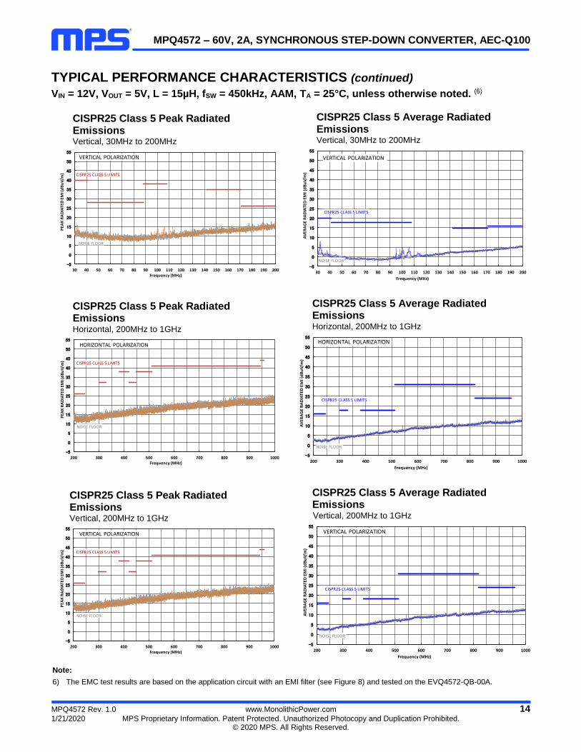
TYPICAL PERFORMANCE CHARACTERISTICS (continued) VIN = 12V, VOUT = 5V, L = 15µH, fSW = 450kHz, AAM, TA = 25°C, unless otherwise noted. (6)
CISPR25 Class 5 Peak Radiated Emissions Vertical, 30MHz to 200MHz
-5
0
5
10
15
20
25
30
35
40
45
50
55
30 40 50 60 70 80 90 100 110 120 130 140 150 160 170 180 190 200
PEA
K R
AD
IATE
D E
MI (
dB
uV
/m)
Frequency (MHz)
CISPR25 CLASS 5 LIMITS
NOISE FLOOR
VERTICAL POLARIZATION
CISPR25 Class 5 Average Radiated Emissions Vertical, 30MHz to 200MHz
-5
0
5
10
15
20
25
30
35
40
45
50
55
30 40 50 60 70 80 90 100 110 120 130 140 150 160 170 180 190 200
AV
ERA
GE
RA
DIA
TED
EM
I (d
Bu
V/m
)
Frequency (MHz)
CISPR25 CLASS 5 LIMITS
NOISE FLOOR
VERTICAL POLARIZATION
CISPR25 Class 5 Peak Radiated Emissions Horizontal, 200MHz to 1GHz
-5
0
5
10
15
20
25
30
35
40
45
50
55
200 300 400 500 600 700 800 900 1000
PEA
K R
AD
IATE
D E
MI (
dB
uV
/m)
Frequency (MHz)
CISPR25 CLASS 5 LIMITS
NOISE FLOOR
HORIZONTAL POLARIZATION
CISPR25 Class 5 Average Radiated Emissions Horizontal, 200MHz to 1GHz
-5
0
5
10
15
20
25
30
35
40
45
50
55
200 300 400 500 600 700 800 900 1000
AV
ERA
GE
RA
DIA
TED
EM
I (d
Bu
V/m
)
Frequency (MHz)
CISPR25 CLASS 5 LIMITS
NOISE FLOOR
HORIZONTAL POLARIZATION
CISPR25 Class 5 Peak Radiated Emissions Vertical, 200MHz to 1GHz
-5
0
5
10
15
20
25
30
35
40
45
50
55
200 300 400 500 600 700 800 900 1000
PEA
K R
AD
IATE
D E
MI (
dB
uV
/m)
Frequency (MHz)
CISPR25 CLASS 5 LIMITS
NOISE FLOOR
VERTICAL POLARIZATION
CISPR25 Class 5 Average Radiated Emissions
Vertical, 200MHz to 1GHz
-5
0
5
10
15
20
25
30
35
40
45
50
55
200 300 400 500 600 700 800 900 1000
AV
ERA
GE
RA
DIA
TED
EM
I (d
Bu
V/m
)
Frequency (MHz)
CISPR25 CLASS 5 LIMITS
NOISE FLOOR
VERTICAL POLARIZATION
Note:
6) The EMC test results are based on the application circuit with an EMI filter (see Figure 8) and tested on the EVQ4572-QB-00A.
MPQ4572 – 60V, 2A, SYNCHRONOUS STEP-DOWN CONVERTER, AEC-Q100
MPQ4572 Rev. 1.0 www.MonolithicPower.com 15
1/21/2020 MPS Proprietary Information. Patent Protected. Unauthorized Photocopy and Duplication Prohibited. © 2020 MPS. All Rights Reserved.
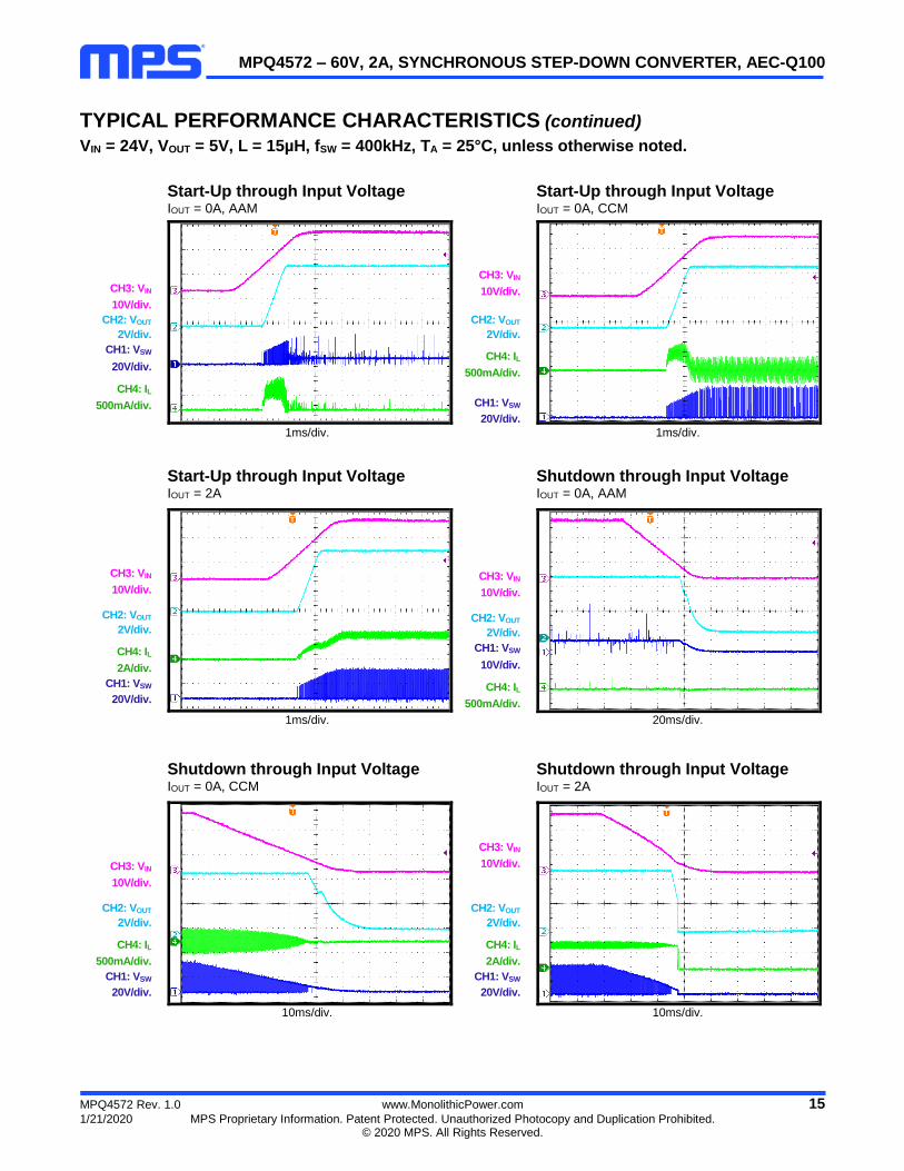
TYPICAL PERFORMANCE CHARACTERISTICS (continued) VIN = 24V, VOUT = 5V, L = 15µH, fSW = 400kHz, TA = 25°C, unless otherwise noted.
Start-Up through Input Voltage IOUT = 0A, AAM
Start-Up through Input Voltage IOUT = 0A, CCM
CH3: VIN
10V/div.
CH2: VOUT
2V/div.
CH1: VSW
20V/div.
CH4: IL
500mA/div.
CH3: VIN
10V/div.
CH2: VOUT
2V/div.
CH4: IL
500mA/div.
CH1: VSW
20V/div. 1ms/div. 1ms/div.
Start-Up through Input Voltage IOUT = 2A
Shutdown through Input Voltage IOUT = 0A, AAM
CH3: VIN
10V/div.
CH2: VOUT
2V/div.
CH4: IL
2A/div.
CH1: VSW
20V/div.
CH3: VIN
10V/div.
CH2: VOUT
2V/div.
CH1: VSW
10V/div.
CH4: IL
500mA/div. 1ms/div. 20ms/div.
Shutdown through Input Voltage IOUT = 0A, CCM
Shutdown through Input Voltage IOUT = 2A
CH3: VIN
10V/div.
CH2: VOUT
2V/div.
CH4: IL
500mA/div.
CH1: VSW
20V/div.
CH3: VIN
10V/div.
CH2: VOUT
2V/div.
CH4: IL
2A/div.
CH1: VSW
20V/div.
10ms/div. 10ms/div.

MPQ4572 – 60V, 2A, SYNCHRONOUS STEP-DOWN CONVERTER, AEC-Q100
MPQ4572 Rev. 1.0 www.MonolithicPower.com 16
1/21/2020 MPS Proprietary Information. Patent Protected. Unauthorized Photocopy and Duplication Prohibited. © 2020 MPS. All Rights Reserved.
TYPICAL PERFORMANCE CHARACTERISTICS (continued) VIN = 24V, VOUT = 5V, L = 15µH, fSW = 400kHz, TA = 25°C, unless otherwise noted.
Start-Up through EN IOUT = 0A, AAM
Start-Up through EN IOUT = 0A, CCM
CH3: VEN
2V/div.
CH2: VOUT
2V/div.
CH1: VSW
20V/div.
CH4: IL
500mA/div.
CH3: VEN
2V/div.
CH2: VOUT
2V/div.
CH4: IL
500mA/div.
CH1: VSW
20V/div. 1ms/div. 1ms/div.
Start-Up through EN IOUT = 2A
Shutdown through EN IOUT = 0A, AAM
CH3: VEN
2V/div.
CH2: VOUT
2V/div.
CH4: IL
2A/div.
CH1: VSW
20V/div.
CH3: VEN
2V/div.
CH2: VOUT
2V/div.
CH1: VSW
10V/div.
CH4: IL
500mA/div. 1ms/div. 1s/div.
Shutdown through EN IOUT = 0A, CCM
Shutdown through EN IOUT = 2A
CH3: VEN
2V/div.
CH2: VOUT
2V/div.
CH4: IL
500mA/div.
CH1: VSW
20V/div.
CH3: VEN
2V/div.
CH2: VOUT
2V/div.
CH4: IL
2A/div.
CH1: VSW
20V/div.
200ms/div. 100μs/div.

MPQ4572 – 60V, 2A, SYNCHRONOUS STEP-DOWN CONVERTER, AEC-Q100
MPQ4572 Rev. 1.0 www.MonolithicPower.com 17
1/21/2020 MPS Proprietary Information. Patent Protected. Unauthorized Photocopy and Duplication Prohibited. © 2020 MPS. All Rights Reserved.
TYPICAL PERFORMANCE CHARACTERISTICS (continued) VIN = 24V, VOUT = 5V, L = 15µH, fSW = 400kHz, TA = 25°C, unless otherwise noted.
Output Ripple IOUT = 0A, AAM
Output Ripple IOUT = 0A, CCM
CH2: VOUT/AC
10mV/div.
CH1: VSW
10V/div.
CH4: IL 500mA/div.
CH1: VSW
10V/div.
CH2:
VOUT/AC
20mV/div.
CH4: IL 1A/div.
400µs/div. 2µs/div.
Output Ripple IOUT = 2A
Short-Circuit Protection (SCP) Entry IOUT = 0A, AAM
CH1: VSW
10V/div.
CH2: VOUT/AC
20mV/div.
CH4: IL 2A/div.
CH2: VOUT
2V/div.
CH3: VPG
5V/div.
CH1: VSW 20V/div.
CH4: IL
2A/div.
2µs/div. 4ms/div.
Short-Circuit Protection (SCP) Entry IOUT = 0A, CCM
Short-Circuit Protection (SCP) Entry IOUT = 2A
CH2: VOUT
2V/div.
CH3: VPG
5V/div.
CH4: IL
2A/div.
CH1: VSW
20V/div.
CH2: VOUT
2V/div.
CH3: VPG
5V/div.
CH4: IL
2A/div.
CH1: VSW
20V/div. 4ms/div. 4ms/div.

MPQ4572 – 60V, 2A, SYNCHRONOUS STEP-DOWN CONVERTER, AEC-Q100
MPQ4572 Rev. 1.0 www.MonolithicPower.com 18
1/21/2020 MPS Proprietary Information. Patent Protected. Unauthorized Photocopy and Duplication Prohibited. © 2020 MPS. All Rights Reserved.
TYPICAL PERFORMANCE CHARACTERISTICS (continued) VIN = 24V, VOUT = 5V, L = 15µH, fSW = 400kHz, TA = 25°C, unless otherwise noted.
Short-Circuit Protection (SCP) Recovery IOUT = 0A, AAM
Short-Circuit Protection (SCP) Recovery IOUT = 0A, CCM
CH2: VOUT
2V/div.
CH3: VPG
5V/div.
CH4: IL
2A/div.
CH1: VSW 20V/div.
CH2: VOUT
2V/div.
CH3: VPG
5V/div.
CH4: IL
2A/div.
CH1: VSW
20V/div. 4ms/div. 4ms/div.
Short-Circuit Protection (SCP) Recovery IOUT = 2A
Short-Circuit Protection (SCP) Steady State
CH2: VOUT
2V/div.
CH3: VPG
5V/div.
CH4: IL
2A/div.
CH1: VSW
20V/div.
CH2: VOUT
2V/div.
CH3: VPG
5V/div.
CH4: IL
2A/div.
CH1: VSW
20V/div.
4ms/div. 4ms/div.
Load Transient IOUT = 0A to 1A, AAM
Load Transient IOUT = 1A to 2A, AAM
CH2:
VOUT/AC
200mV/div.
CH4: IOUT
500mA/div.
CH2:
VOUT/AC
200mV/div.
CH4: IOUT
1A/div.
100µs/div. 100µs/div.

MPQ4572 – 60V, 2A, SYNCHRONOUS STEP-DOWN CONVERTER, AEC-Q100
MPQ4572 Rev. 1.0 www.MonolithicPower.com 19
1/21/2020 MPS Proprietary Information. Patent Protected. Unauthorized Photocopy and Duplication Prohibited. © 2020 MPS. All Rights Reserved.
TYPICAL PERFORMANCE CHARACTERISTICS (continued) VIN = 24V, VOUT = 5V, L = 15µH, fSW = 400kHz, TA = 25°C, unless otherwise noted.
Cold Crank VIN = 24V to 4V to 5V, IOUT = 0A
Cold Crank VIN = 24V to 4V to 5V, IOUT = 2A
CH3: VIN
10V/div.
CH1: VSW
10V/div.
CH2: VOUT
5V/div.
CH4: IL
500mA/div.
CH3: VIN
10V/div.
CH1: VSW
10V/div.
CH2: VOUT
5V/div.
CH4: IL
2A/div.
40ms/div. 40ms/div.
VIN Ramp Down and Up VIN = 18V to 4.5V to 0V to 4.5V to 18V, IOUT = 0A
VIN Ramp Down and Up VIN = 18V to 4.5V to 0V to 4.5V to 18V, IOUT = 2A
CH3: VIN
5V/div.
CH1: VSW
5V/div.
CH2: VOUT
5V/div.
CH4: IL
2A/div.
CH3: VIN
5V/div.
CH1: VSW
5V/div.
CH2: VOUT
5V/div.
CH4: IL
2A/div. 10s/div. 10s/div.
Load Dump VIN = 24V to 48V to 24V, IOUT = 2A
CH3: VIN
20V/div.
CH1: VSW
20V/div.
CH2: VOUT
5V/div.
CH4: IL
2A/div.
100ms/div.
MPQ4572 – 60V, 2A, SYNCHRONOUS STEP-DOWN CONVERTER, AEC-Q100
MPQ4572 Rev. 1.0 www.MonolithicPower.com 20
1/21/2020 MPS Proprietary Information. Patent Protected. Unauthorized Photocopy and Duplication Prohibited. © 2020 MPS. All Rights Reserved.
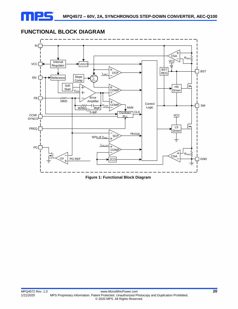
FUNCTIONAL BLOCK DIAGRAM
UVLOVCC
IN
FB Error
Amplifier
VREF
Internal
Regulator
Soft
Start
Slope
Comp
OCPILIMIT
Control
LogicSW
CSA
CSA
COMP
IVALLEY
SCPHiccup
PG REF
50% of VREF
COMP
GND
CLK
Reference
BSTBST
REG
ZCD
Oscillator
PLL
PG
HS
Driver
LS
Driver
RSEN
RSEN
VCC
UV
EN
CCM/
SYNCO
FREQ
VCC
COMPVAAMAAM
18kΩ
600kΩ
0.4pF
36pF
Figure 1: Functional Block Diagram
MPQ4572 – 60V, 2A, SYNCHRONOUS STEP-DOWN CONVERTER, AEC-Q100
MPQ4572 Rev. 1.0 www.MonolithicPower.com 21
1/21/2020 MPS Proprietary Information. Patent Protected. Unauthorized Photocopy and Duplication Prohibited. © 2020 MPS. All Rights Reserved.
OPERATION The MPQ4572 is a fully integrated, synchronous, rectified, step-down, non-isolated switch-mode converter. It is available with a wide 4.5V to 60V input supply range, and can achieve up to 2A of continuous output current with excellent load and line regulation over an ambient temperature range of -40°C to +125°C. Figure 1 shows a block diagram of the device.
PWM Control
At moderate to high output currents, the MPQ4572 operates in a fixed-frequency, peak current control mode to regulate the output voltage.
An internal clock initiates a PWM cycle. At the rising edge of the clock, the high-side switch (HS-FET) turns on, and the inductor current rises linearly to provide energy to the load. The HS-FET remains on until its current reaches the value set by the COMP voltage (VCOMP), which is the output of the internal error amplifier. VCOMP is based on the difference between the output feedback voltage and internal high-precision reference. VCOMP determines how much energy should be transferred to the load. A higher load current creates a higher VCOMP. Once the HS-FET is on, it remains on for at least 90ns.
When the HS-FET is off, the low-side switch (LS-FET) turns on immediately, and stays on until the next clock starts. During this time, the inductor current flows through the LS-FET. Once the LS-FET is on, it remains on for at least 100ns before the next cycle starts. To avoid shoot-through, a dead time is inserted to prevent the HS-FET and LS-FET from turning on simultaneously.
If the current in the HS-FET does not reach the value set by COMP within one PWM period, the HS-FET remains on, saving a turn-off operation.
Light-Load Operation
The MPQ4572 features configurable forced continuous conduction mode (FCCM) and light-load asynchronous advanced mode (AAM), which can be set by the CCM/SYNCO pin. FCCM maintains a constant switching frequency and smaller output ripple. However, FCCM has low efficiency during light-load conditions, while AAM achieves high efficiency (see Figure 2).
To force the device into FCCM, connect the CCM/SYNCO pin to GND using a resistor between 10kΩ and 300kΩ. In FCCM, the converter works with a fixed frequency across a no-load to full-load range. Float the CCM/SYNCO pin to force the device into AAM under light-load conditions. The device cannot change modes while it is operating, so the mode must be selected before start-up.
When AAM is enabled, the switching frequency is scaled down according to VCOMP during light-load conditions. The MPQ4572 first enters non-synchronous operation while the inductor current approaches zero at light-load. If the load further decreases or is at no-load, VCOMP drops below the internally set AAM value (VAAM). The MPQ4572 then enters sleep mode and consumes a low quiescent current to improve light-load efficiency.
In sleep mode, the internal clock is blocked, so the MPQ4572 skips some pulses. VFB is below VREF, so VCOMP ramps up until it exceeds VAAM. Then the internal clock is reset and the crossover time is used as a benchmark for the next clock. This control scheme helps the device achieve high efficiency by scaling down the frequency to reduce the switching and gate driver losses.
As the output current increases from light-load, both VCOMP and the switching frequency rise. If the output current exceeds the critical level set by VCOMP, the MPQ4572 enters discontinuous conduction operation (DCM) or CCM, which has a constant switching frequency.
AAMInductor
Current
t
t
t
Load
Decreased
FCCMInductor
Current
t
t
t
Load
Decreased
Figure 2: AAM and FCCM
Enable (EN) Control
The MPQ4572 can be enabled or disabled via a remote EN signal that is referenced to ground. The remote EN control operates with a positive logic that is compatible with popular logic devices.

MPQ4572 – 60V, 2A, SYNCHRONOUS STEP-DOWN CONVERTER, AEC-Q100
MPQ4572 Rev. 1.0 www.MonolithicPower.com 22
1/21/2020 MPS Proprietary Information. Patent Protected. Unauthorized Photocopy and Duplication Prohibited. © 2020 MPS. All Rights Reserved.
Positive logic indicates that when the input voltage exceeds the under-voltage lockout (UVLO) threshold (about 4.0V), the converter is enabled by pulling the EN pin above 1.45V. Drive the EN pin below 1.12V to disable the MPQ4572. An internal resistor (REN) from EN to GND allows EN to be floated to shut down the chip (REN = 2.8MΩ when EN is on; REN = 1.8MΩ when EN is off).
SYNC OUT (SYNCO)
The MPQ4572 has a SYNCO pin. During start-up, SYNCO stays low and quickly outputs a 180° phase-shift clock to the internal oscillator once soft start is ready. Note that the falling edge of SYNCO is a 180° phase-shift to the rising edge of the internal oscillator. This function allows two devices to operate in the same frequency, but 180° out of phase, which reduces the total input current ripple. This allows a smaller input bypass capacitor to be used.
Internal Regulator
A 4.9V internal regulator powers most of the internal circuitries. This regulator takes VIN and operates in the full VIN range. When VIN exceeds 4.9V, the output of the regulator is in full regulation. Lower VIN values result in lower output voltages. The regulator is enabled when VIN exceeds its UVLO threshold and EN is high. In EN shutdown mode, the internal VCC regulator is disabled to reduce power dissipation.
Frequency Programmable and Foldback
The oscillating frequency (fSW) of the MPQ4572 is programmed by an external frequency resistor. The frequency resistor should be located between the FREQ pin and GND, as close as possible to the device. Select a proper RFREQ, calculated with Equation (1):
(kHz)f
30MR
SW
FREQ )Ω( (1)
The calculated resistance may need fine tuning with a bench test.
It is not possible to use a high fsw with a high VIN, since the minimum on time required for the HS-FET is limited. The MPQ4572 control loop automatically sets the maximum possible fSW up to the set frequency, which also reduces excessive power loss in the IC. VOUT is regulated by varying the duration of the switch-off time of the HS-FET, which results in an automatic reduction of fSW.
Compliance with the minimum on time of the HS-FET is guaranteed. An advantage of this method is that the device works at the desired fSW as long as possible, and a correction is only made at high VIN. For the Switching Frequency vs. VIN curve, see the Typical Performance Characteristics section on page 11, where RFREQ equals 12.1kHz.
Internal Soft Start (SS)
To avoid overshoot during start-up, the MPQ4572 has built-in soft start (SS) that ramps up the output voltage at a controlled slew rate when the EN pin goes high. When the SS voltage (VSS) is below the internal reference (VREF), VSS overrides VREF as the error amplifier reference. When VSS exceeds VREF, VREF acts as the reference. At this point, soft start finishes, and the MPQ4572 enters steady-state.
The SS time is internally set to 0.45ms. When the output voltage is shorted to GND, the feedback voltage is pulled low, then VSS is discharged. The part will soft start again when it returns to the normal state.
Pre-Biased Start-Up
If VFB exceeds VSS during start-up, the output has a pre-biased voltage and neither the HS-FET nor LS-FET turns on until VSS exceeds VFB. Note that this capability is only available when the device is set to AAM.
Power Good (PG) Indicator
The MPQ4572 has power good (PG) indication. The PG pin is the open drain of a MOSFET. It should be connected to a voltage source through a resistor (e.g. 100kΩ). In the presence of an input voltage, the MOSFET turns on so that the PG pin is pulled to GND before soft start is ready. PG goes high if the output voltage is within 90% to 108% of the nominal voltage after a 70μs delay. PG goes low when the output voltage is above 116% or below 84% of the nominal voltage after a 25μs delay.
Under-Voltage Lock-Out (UVLO) Protection
The MPQ4572 has input under-voltage lockout protection (UVLO) to ensure reliable output power. Assuming EN is active, the MPQ4572 is powered on when the input voltage exceeds the UVLO rising threshold. The device is powered off when input voltage drops below the UVLO falling threshold. This function prevents the device from

MPQ4572 – 60V, 2A, SYNCHRONOUS STEP-DOWN CONVERTER, AEC-Q100
MPQ4572 Rev. 1.0 www.MonolithicPower.com 23
1/21/2020 MPS Proprietary Information. Patent Protected. Unauthorized Photocopy and Duplication Prohibited. © 2020 MPS. All Rights Reserved.
operating at an insufficient voltage. It is a non-latch protection.
Over-Current Protection (OCP)
The MPQ4572 has a 3.5A peak current limit. Once the inductor current reaches the current limit, the HS-FET turns off immediately. Then the LS-FET turns on to discharge the energy, and the inductor current decreases. The HS-FET does not turn on again until the inductor current drops below a current threshold (the valley current limit). This protection prevents the inductor current from running away and damaging the components.
Short-Circuit Protection (SCP)
When a short-circuit condition occurs, the MPQ4572 hits its current limit immediately. Meanwhile, the output voltage drops until VFB falls below 50% of VREF. The device considers this an output dead short, and triggers hiccup short-circuit protection (SCP) mode to periodically restart the part.
In hiccup mode, the MPQ4572 disables its output power stage, slowly discharges the soft-start capacitor, and then initiates a soft start. If the short-circuit condition remains after soft start ends, the device repeats this operation until the short circuit disappears and the output returns to the regulation level. This protection mode greatly reduces the average short-circuit current to alleviate thermal issues and protect the regulator.
Negative Current Protection
The MPQ4572 has a -1.3A negative current limit. Once the inductor current reaches the current limit, the LS-FET immediately turns off and the HS-FET turns on. The current limit prevents the negative current from dropping too low and damaging the components.
Thermal Shutdown
For thermal protection, the MPQ4572 monitors the IC temperature internally. This function prevents the chip from operating at exceedingly high temperatures. If the junction temperature exceeds the threshold value (about 170°C), it shuts down the whole chip. This is a non-latch protection. There is a 25°C hysteresis. Once the junction temperature drops to about 145°C, the device resumes operation by initiating a soft start.
Floating Driver and Bootstrap Charging
An external bootstrap capacitor powers the floating HS-FET driver. There are two methods to charge the bootstrap capacitor (see Figure 3).
The first method is through the main charging circuit from VCC through a diode. When the HS-FET is on, VSW is about equal to VIN but exceeds VCC, and the bootstrap capacitor is not charged. The best charging period occurs when the LS-FET is on, and VCC - VSW is at its largest. When there is no current in the inductor, VSW equals VOUT, so VCC can only charge BST when VOUT is very small.
The second method is through the auxiliary charging circuit from VIN. When the voltage difference between BST and SW is below the internal 5V bootstrap regulator, a PMOS pass transistor (M1) turns on to charge the bootstrap capacitor. The charging current is much smaller than that from VCC, but as long as VIN exceeds VSW, BST can be charged. This function is useful in sleep mode, when there is not always a switch.
Figure 3: Internal Bootstrap Charging Circuit
Low-Dropout Operation (BST Refresh)
To improve dropout, the MPQ4572 is designed to operate at close to 100% duty cycle as long as the BST-to-SW voltage exceeds 1.4V. When the BST-to-SW voltage drops below 1.34V, the HS-FET turns off using a UVLO circuit, which allows the LS-FET to conduct and refresh the charge on the BST capacitor. When the input voltage drops, the HS-FET remains on and close to 100% duty cycle to maintain output regulation, until the BST-to-SW voltage falls below 1.34V.
Since the supply current sourced from the BST capacitor is low, the HS-FET can remain on for more switching cycles than are required to refresh the capacitor. The means the effective duty cycle of the switching regulator is high.

MPQ4572 – 60V, 2A, SYNCHRONOUS STEP-DOWN CONVERTER, AEC-Q100
MPQ4572 Rev. 1.0 www.MonolithicPower.com 24
1/21/2020 MPS Proprietary Information. Patent Protected. Unauthorized Photocopy and Duplication Prohibited. © 2020 MPS. All Rights Reserved.
The effective duty cycle during regulator dropout is mostly influenced by the voltage drops across the power MOSFET, inductor resistance, low-side diode, and PCB resistance.
Start-Up and Shutdown
If both VIN and VEN exceed their respective thresholds, the chip starts. The reference block starts first, generating a stable reference voltage and current, and then the internal regulator is enabled. The regulator provides a stable supply for the remaining circuitries.
While the internal supply rail is up, an internal timer holds the power MOSFET off for about 50µs to blank the start-up glitches. When the soft-start block is enabled, it first holds its SS output low to ensure the circuitries are ready, and then slowly ramps up.
Three events can shut down the chip: EN going low, VIN UVLO, and thermal shutdown. In the shutdown procedure, the signaling path is first blocked to avoid any fault triggering. The COMP voltage and the internal supply rail are then pulled down. The floating driver is not subject to this shutdown command, but its charging path is disabled.

MPQ4572 – 60V, 2A, SYNCHRONOUS STEP-DOWN CONVERTER, AEC-Q100
MPQ4572 Rev. 1.0 www.MonolithicPower.com 25
1/21/2020 MPS Proprietary Information. Patent Protected. Unauthorized Photocopy and Duplication Prohibited. © 2020 MPS. All Rights Reserved.
APPLICATION INFORMATION Setting the Output Voltage
The external resistor divider connected to the FB pin sets the output voltage (see the Typical Application section on page 29). The feedback resistor (R1) must account for both stability and dynamic response, so it cannot be too large or too small. Choose an R1 value of about 40kΩ. R2 is then estimated with Equation (2):
OUT
R1R2
V1
0.8
(2)
Figure 4 shows the recommended T-type feedback network.
R1
R2
VOUTFB
MPQ4572
R35
Figure 4: Feedback Network
R3 + R1 is used to set the loop bandwidth. A higher R3 + R1 indicates a lower bandwidth. To ensure loop stability, it is strongly recommended to limit the bandwidth below 1/10 of the switching frequency, and no higher than 100kHz.
The calculated resistance may need fine-tuning via bench testing. Table 1 lists the recommended feedback divider resistor values for common output voltages. Use check loop analysis before using the device in an application, and change the resistance of R3 for loop stability if necessary.
Table 1: Resistor Values for Typical VOUT
VOUT (V) R1 (kΩ) R2 (kΩ)
3.3 41.2 13
5.0 41.2 7.68
Selecting the Inductor
The inductor must supply constant current to the output load while being driven by the switching input voltage. For the highest efficiency, choose an inductor with a low DC resistance. High inductance will result in less ripple current and lower output ripple voltage. However, a larger inductance value results in a physically larger
inductor, higher series resistance, and lower saturation current.
A good rule to determine the ideal inductance value is to allow the inductor ripple current to be approximately 30% of the maximum load current. Ensure that the peak inductor current is below the device peak current limit. The inductance value can be calculated with Equation (3):
OUT OUT
SW L IN
V VL (1 )
f I V (3)
Where ΔIL is the peak-to-peak inductor ripple current.
Choose an inductor that will not saturate under the maximum inductor peak current. Calculate the peak inductor current with Equation (4):
OUT OUTLP OUT
SW IN
V VI I (1 )
2f L V (4)
Selecting the Input Capacitor
The step-down converter has a discontinuous input current, and requires a capacitor to supply the AC current to the converter while maintaining the DC input voltage. Use low-ESR capacitors for the best performance. Ceramic capacitors with X5R or X7R dielectrics are strongly recommended because of their low ESR and small temperature coefficients. Other capacitors, such as Y5V and Z5U, should not be used since they lose too much capacitance with frequency, temperature, and bias voltage.
Place the input capacitors as close to the IN pin as possible. For most applications, a 22µF capacitor is sufficient. For higher output voltages, use a 47μF capacitor to improve system stability. To maintain a small solution size, choose a properly sized capacitor that has a voltage rating compliant with the input spec.
Since the input capacitor absorbs the input switching current, it requires an adequate ripple current rating, which should not exceed the converter’s maximum input ripple current. The input ripple current can be estimated with Equation (5):
OUT OUTCIN OUT
IN IN
V VI I (1 )
V V (5)

MPQ4572 – 60V, 2A, SYNCHRONOUS STEP-DOWN CONVERTER, AEC-Q100
MPQ4572 Rev. 1.0 www.MonolithicPower.com 26
1/21/2020 MPS Proprietary Information. Patent Protected. Unauthorized Photocopy and Duplication Prohibited. © 2020 MPS. All Rights Reserved.
The worst-case condition occurs at VIN = 2VOUT, calculated with Equation (6):
OUTCIN
II
2 (6)
For simplification, choose an input capacitor with an RMS current rating greater than half of the maximum load current.
The input capacitor can be electrolytic, tantalum, or ceramic. When using electrolytic or tantalum capacitors, use a small, high-quality ceramic capacitor (0.1μF), placed as close to the IC as possible. The input capacitance value determines the input voltage ripple of the converter. If there is an input voltage ripple requirement in the system design, choose an input capacitor that meets the specification.
The input voltage ripple caused by the capacitance can be estimated with Equation (7):
OUT OUT OUTIN
SW IN IN IN
I V VV (1 )
f C V V (7)
The worst-case condition occurs at VIN = 2VOUT, estimated with Equation (8):
OUTIN
SW IN
I1V
4 f C (8)
Selecting the Output Capacitor
The output capacitor maintains the output DC voltage. Ceramic capacitors with low ESR are recommended for a small size and low output voltage ripple. Electrolytic and polymer capacitors may also be used. The output voltage ripple can be estimated with Equation (9):
OUT OUTOUT ESR
SW IN SW OUT
V V 1V (1 ) (R )
f L V 8f C
(9)
Where RESR is the equivalent series resistance of the output capacitor.
For ceramic capacitors, the capacitance dominates the impedance at the switching frequency and causes most of the output voltage ripple. For simplification, the output voltage ripple can be calculated with Equation (10):
OUT OUTOUT 2
SW OUT IN
V VV (1 )
8 f L C V (10)
For tantalum or electrolytic capacitors, the ESR dominates the impedance at the switching frequency. For simplification, the output ripple can be calculated with Equation (11):
OUT OUTOUT ESR
SW IN
V VV (1 ) R
f L V (11)
Another consideration for output capacitance is the allowable overshoot in VOUT if the load is suddenly removed. In this case, energy stored in the inductor is transferred to COUT, causing its voltage to rise. To achieve a desired overshoot relative to the regulated voltage, the output capacitance can be estimated with Equation (12):
2
OUTOUT 2 2
OUT OUTMAX OUT
I LC
V ((V / V ) 1) (12)
Where VOUTMAX / VOUT is the allowable maximum overshoot.
After calculating the capacitance required for both ripple and overshoot needs, choose the larger value.
The characteristics of the output capacitor also affect the stability of the regulation system. The MPQ4572 can be optimized for a wide range of capacitance and ESR values.
VIN Under-Voltage Lockout (UVLO) Setting
The MPQ4572 has an internal, fixed UVLO threshold. The rising threshold is 4.0V, while the falling threshold is about 3.5V. For applications that require a higher UVLO point, place an external resistor divider between EN and IN to obtain a higher equivalent UVLO threshold (see Figure 5 and Figure 6). Add a 6V Zener diode between EN to GND if the EN pin is connected to VIN through a resistor.
VIN
EN
IN
R4
1.8MΩ R5
8
12
6V
Zener
Figure 5: Adjustable UVLO Using EN Divider when EN Rises

MPQ4572 – 60V, 2A, SYNCHRONOUS STEP-DOWN CONVERTER, AEC-Q100
MPQ4572 Rev. 1.0 www.MonolithicPower.com 27
1/21/2020 MPS Proprietary Information. Patent Protected. Unauthorized Photocopy and Duplication Prohibited. © 2020 MPS. All Rights Reserved.
VIN
EN
IN
R4
2.8MΩ R5
8
12
6V
Zener
Figure 6: Adjustable UVLO Using EN Divider when EN Falling
The UVLO threshold can be calculated with Equation (13) and Equation (14) when EN is rising or falling, respectively:
EN_RISINGRISING V
1.8M//R5
R4(1INUV ) (13)
EN_FALLINGFALLING V
2.8M//R5
R4(1INUV ) (14)
Where VEN_RISING = 1.45V, VEN_FALLING = 1.12V.
When choosing R4, ensure it is big enough to limit the current flowing into EN pin below 100µA.
BST Resistor and Capacitor A resistor in series with the BST capacitor (RBST) can reduce the SW rising rate and voltage spikes. This enhances EMI performance and reduces voltage stress at a high VIN. A higher resistance is better for SW spike reduction, but compromises efficiency. To make a tradeoff between EMI and efficiency, it is recommended to keep RBST below 20Ω. The recommended BST capacitor value is between 0.1µF and 1μF.

MPQ4572 – 60V, 2A, SYNCHRONOUS STEP-DOWN CONVERTER, AEC-Q100
MPQ4572 Rev. 1.0 www.MonolithicPower.com 28
1/21/2020 MPS Proprietary Information. Patent Protected. Unauthorized Photocopy and Duplication Prohibited. © 2020 MPS. All Rights Reserved.
PCB Layout Guidelines (7)
An optimized PCB layout is very important for proper operation. A 4-layer layout is strongly recommended to improve thermal performance. For the best results, refer to Figure 7 and follow the guidelines below:
1. Place the high-current paths (GND, IN, and SW) very close to the device with short, direct, and wide traces.
2. Use large copper areas to minimize conduction loss and thermal stress.
3. Place the ceramic input capacitors as close to the IN and GND pins as possible to minimize high-frequency noise.
4. Place the T-type feedback resistors as close as possible to the FB pin to ensure that the trace connecting to the FB pin is as short as possible.
5. Route SW and BST away from sensitive analog areas, such as FB.
6. Use multiple vias to connect the power planes to internal layer.
Note:
7) The recommended PCB layout is based on the circuit in Figure 8.
Top Layer and Top Silk
Inner Layer 1
Inner Layer 2
Bottom Layer and Bottom Silk
Figure 7: Recommended PCB Layout

MPQ4572 – 60V, 2A, SYNCHRONOUS STEP-DOWN CONVERTER, AEC-Q100
MPQ4572 Rev. 1.0 www.MonolithicPower.com 29
1/21/2020 MPS Proprietary Information. Patent Protected. Unauthorized Photocopy and Duplication Prohibited. © 2020 MPS. All Rights Reserved.
TYPICAL APPLICATION CIRCUIT
EN
GND
VOUT
100kΩ R1
10µF
C1A22µF
C2A
22µF
C2B
15µH
L3
10µF
C1B
5V/2A
0.1µF
C1C
76.8kΩ
R11
CCM/SYNCO
PG
41.2kΩ
R4
20kΩ
R6
7.68kΩ
R5
1µF
C3
100kΩ
R9
IN8
FREQ5
PG3
SW2
CCM/SYNCO11
VCC6
EN12
GN
D7
BS
T1
FB4
U1
MPQ4572
0.1µF
C4
1
2
JP1
100kΩ R10
GND
VEMI
22µF
CIN9
1210 1210 06030.1µF
C1D
0603
D1
BZT52C6V2
Figure 8: Typical Application Circuit
EN
GND
VOUT
100kΩ R1
10µF
C1A
22µFC2A
22µFC2B
15µHL3
10µF
C1B
5V to 60V
5V/2A
0.1µF
C1C
76.8kΩ
R11
CCM/SYNCO
10nFC2D
PG
41.2kΩ
R4
20kΩ R6
7.68kΩ R5
1nFC2C
1µFC3
100kΩ R9
IN8
FREQ5P
G3
SW2
CCM/SYNCO11
VCC6
EN12
GN
D7
BS
T1
FB4
U1
MPQ4572
0.1µF
C4
1
2
JP1
100kΩ
R10
10nFC2F
1nFC2E0.1µF/100V
C12 R2310Ω/0603
0.1µF
C10 R20
10Ω
0.1µF
C11 R21
10Ω
VOUT
GND
VEMI
240nHL1
22µF
CIN9
4.7µHL2
10µF
CIN7
1nF
CIN1
10nF
CIN2
1nF
CIN3
10nF
CIN4
0603 0603 0603 06031µF
CIN5
1µF
CIN6
0805 0805 121010µF
CIN8
1210 1210 1210 06030.1µF
C1D
0603
VIN
VIN
D1BZT52C6V2
VOUT
DFE201612E-R24M FDSD0402-H-4R7M
Figure 9: Typical Application Circuit with EMI Filters

MPQ4572 – 60V, 2A, SYNCHRONOUS STEP-DOWN CONVERTER, AEC-Q100
MPQ4572 Rev. 1.0 www.MonolithicPower.com 30
1/21/2020 MPS Proprietary Information. Patent Protected. Unauthorized Photocopy and Duplication Prohibited. © 2020 MPS. All Rights Reserved.
PACKAGE INFORMATION
QFN-12 (2.5mmx3mm) Non-Wettable Flank
SIDE VIEW
BOTTOM VIEW
NOTE:
1) LAND PATTERNS OF PINS 2, 7, AND 8
HAVE THE SAME LENGTH AND WIDTH.
2) ALL DIMENSIONS ARE IN MILLIMETERS.
3) LEAD COPLANARITY SHALL BE 0.10
MILLIMETERS MAX.
4) JEDEC REFERENCE IS MO-220.
5) DRAWING IS NOT TO SCALE.
PIN 1 ID
MARKING
TOP VIEW
PIN 1 ID
INDEX AREA
RECOMMENDED LAND PATTERN
QFN-12 (2.5mmX3mm)

MPQ4572 – 60V, 2A, SYNCHRONOUS STEP-DOWN CONVERTER, AEC-Q100
MPQ4572 Rev. 1.0 www.MonolithicPower.com 31
1/21/2020 MPS Proprietary Information. Patent Protected. Unauthorized Photocopy and Duplication Prohibited. © 2020 MPS. All Rights Reserved.
PACKAGE INFORMATION (continued)
QFN-12 (2.5mmx3mm) Wettable Flank
PACKAGE OUTLINE DRAWING FOR 12L FCQFN (2.5X3.0MM)-3
MF-PO-D-0484 revision 0.0
SIDE VIEW
BOTTOM VIEW
NOTE:
1) THE LEAD SIDE IS WETTABLE.
2) LAND PATTERNS OF PINS 2, 7, AND 8
HAVE THE SAME LENGTH AND WIDTH.
3) ALL DIMENSIONS ARE IN MILLIMETERS.
4) LEAD COPLANARITY SHALL BE 0.08
MILLIMETERS MAX.
5) JEDEC REFERENCE IS MO-220.
6) DRAWING IS NOT TO SCALE.
PIN 1 ID
MARKING
TOP VIEW
PIN 1 ID
INDEX AREA
RECOMMENDED LAND PATTERN
SECTION A-A

MPQ4572 – 60V, 2A, SYNCHRONOUS STEP-DOWN CONVERTER, AEC-Q100
Notice: The information in this document is subject to change without notice. Please contact MPS for current specifications.
Users should warrant and guarantee that third-party Intellectual Property rights are not infringed upon when integrating MPS products into any application. MPS will not assume any legal responsibility for any said applications.
MPQ4572 Rev. 1.0 www.MonolithicPower.com 32 1/21/2020 MPS Proprietary Information. Patent Protected. Unauthorized Photocopy and Duplication Prohibited. © 2020 MPS. All Rights Reserved.
CARRIER INFORMATION
Part Number Package
Description Quantity/Reel Reel Diameter
Carrier Tape Width
Carrier Tape Pitch
MPQ4572GQB-Z QFN-12
(2.5mmx3mm) 5000 13in 12mm 8mm MPQ4572GQB-AEC1-Z
MPQ4572GQBE-AEC1-Z