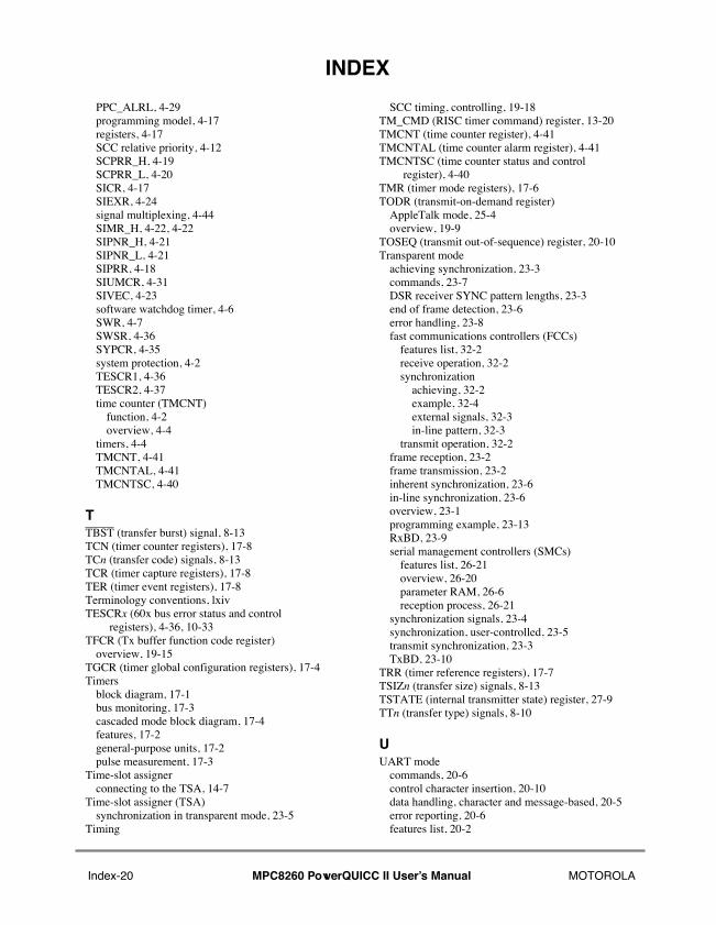
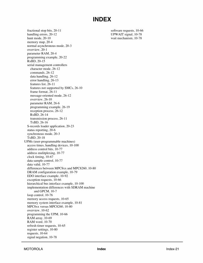
mpc8260 powerquicc ii user•s manual - the freebsd project
TRANSCRIPT
MPC8260UM/D4/1999Rev. 0
MPC8260 PowerQUICC IIUserÕs Manual
ª
ª
PowerQUICC II, Mfax, and DigitalDNA are trademarks of Motorola, Inc. The PowerPC name, the PowerPC logotype, PowerPC 601, PowerPC 603, PowerPC 603e, PowerPC 604, PowerPC 604e, and RS/6000 are trademarks ofInternational Business Machines Corporation used by Motorola under license from International Business Machines Corporation.I
2
C is a registered trademark of Philips Semiconductors
Information in this document is provided solely to enable system and software implementers to use PowerPC microprocessors. There are no express or impliedcopyright licenses granted hereunder to design or fabricate PowerPC integrated circuits or integrated circuits based on the information in this document.
Motorola reserves the right to make changes without further notice to any products herein. Motorola makes no warranty, representation or guaranteeregarding the suitability of its products for any particular purpose, nor does Motorola assume any liability arising out of the application or use of any product orcircuit, and specifically disclaims any and all liability, including without limitation consequential or incidental damages. ÒTypicalÓ parameters can and do vary indifferent applications. All operating parameters, including ÒTypicalsÓ must be validated for each customer application by customerÕs technical experts. Motoroladoes not convey any license under its patent rights nor the rights of others. Motorola products are not designed, intended, or authorized for use as componentsin systems intended for surgical implant into the body, or other applications intended to support or sustain life, or for any other application in which the failureof the Motorola product could create a situation where personal injury or death may occur. Should Buyer purchase or use Motorola products for any suchunintended or unauthorized application, Buyer shall indemnify and hold Motorola and its officers, employees, subsidiaries, affiliates, and distributors harmlessagainst all claims, costs, damages, and expenses, and reasonable attorney fees arising out of, directly or indirectly, any claim of personal injury or deathassociated with such unintended or unauthorized use, even if such claim alleges that Motorola was negligent regarding the design or manufacture of the part.
Motorola and are registered trademarks of Motorola, Inc. Motorola, Inc. is an Equal Opportunity/AfÞrmative Action Employer.
Motorola Literature Distribution Centers
:
USA/EUROPE:
Motorola Literature Distribution; P.O. Box 5405; Denver, Colorado 80217; Tel.: 1-800-441-2447 or 1-303-675-2140
JAPAN
: Nippon Motorola Ltd SPD, Strategic Planning Office 4-32-1, Nishi-Gotanda Shinagawa-ku, Tokyo 141, Japan Tel.: 81-3-5487-8488
ASIA/PACIFC
: Motorola Semiconductors H.K. Ltd.; 8B Tai Ping Industrial Park, 51 Ting Kok Road, Tai Po, N.T., Hong Kong; Tel.: 852-26629298
Mfaxª
: [email protected]; TOUCHTONE 1-602-244-6609; US & Canada ONLY (800) 774-1848;
World Wide Web Address
: http://sps.motorola.com/mfax
INTERNET
: http://motorola.com/sps
Technical Information
: Motorola Inc. SPS Customer Support Center; 1-800-521-6274; electronic mail address: [email protected].
Document Comments
: FAX (512) 895-2638, Attn: RISC Applications Engineering.
World Wide Web Addresses
: http://www.mot.com/PowerPChttp://www.mot.com/netcommhttp://www.mot.com/HPESD
© Motorola, Inc., 1999. All rights reserved.

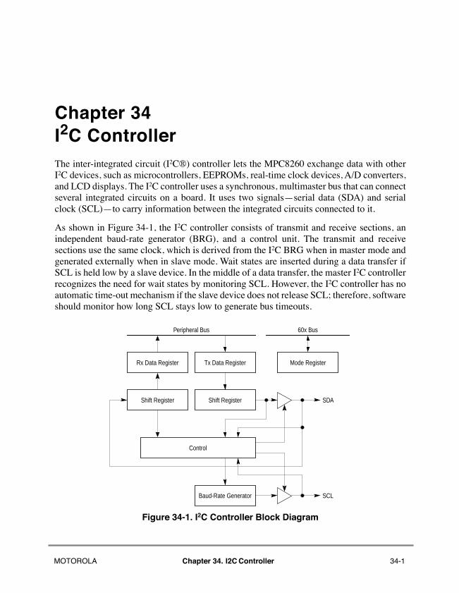
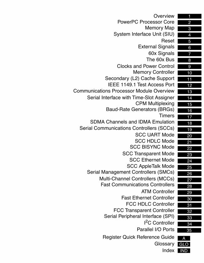
OverviewPowerPC Processor Core
Memory MapSystem Interface Unit (SIU)
ResetExternal Signals
60x SignalsThe 60x Bus
Clocks and Power ControlMemory Controller
Secondary (L2) Cache SupportIEEE 1149.1 Test Access Port
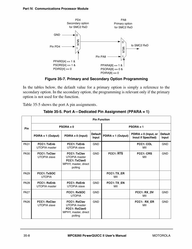
Communications Processor Module OverviewSerial Interface with Time-Slot Assigner
CPM MultiplexingBaud-Rate Generators (BRGs)
TimersSDMA Channels and IDMA Emulation
Serial Communications Controllers (SCCs)SCC UART ModeSCC HDLC Mode
SCC BISYNC ModeSCC Transparent Mode
SCC Ethernet ModeSCC AppleTalk Mode
Serial Management Controllers (SMCs)Multi-Channel Controllers (MCCs)Fast Communications Controllers
ATM ControllerFast Ethernet Controller
FCC HDLC ControllerFCC Transparent Controller
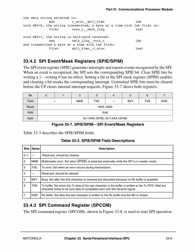
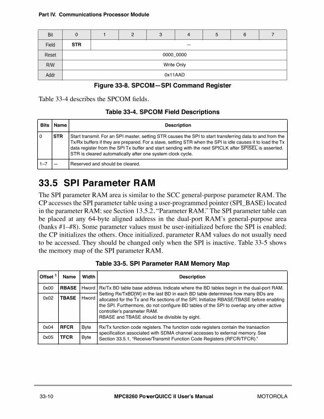
Serial Peripheral Interface (SPI)I
2
C ControllerParallel I/O Ports
Register Quick Reference GuideGlossary
Index
3
4
5
6
7
8
9
10
1
GLO
IND
12
13
14
15
16
17
18
19
11
20
22
23
24
25
26
27
28
29
21
30
32
33
34
31
35
2
A

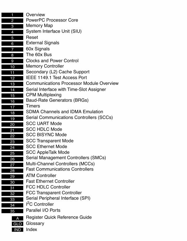
OverviewPowerPC Processor CoreMemory MapSystem Interface Unit (SIU)ResetExternal Signals60x SignalsThe 60x BusClocks and Power ControlMemory ControllerSecondary (L2) Cache SupportIEEE 1149.1 Test Access PortCommunications Processor Module OverviewSerial Interface with Time-Slot AssignerCPM MultiplexingBaud-Rate Generators (BRGs)TimersSDMA Channels and IDMA EmulationSerial Communications Controllers (SCCs)SCC UART ModeSCC HDLC ModeSCC BISYNC ModeSCC Transparent ModeSCC Ethernet ModeSCC AppleTalk ModeSerial Management Controllers (SMCs)Multi-Channel Controllers (MCCs)Fast Communications ControllersATM ControllerFast Ethernet ControllerFCC HDLC ControllerFCC Transparent ControllerSerial Peripheral Interface (SPI)I
2
C ControllerParallel I/O Ports
Register Quick Reference GuideGlossaryIndex
3
4
5
6
7
8
9
10
1
GLO
IND
12
13
14
15
16
17
18
19
11
20
22
23
24
25
26
27
28
29
21
30
32
33
34
31
35
2
A
CONTENTS
ParagraphNumber Title Page
Number
About This Book
Before Using this ManualÑImportant Note.......................................................... lvAudience ................................................................................................................ lvOrganization.......................................................................................................... lviSuggested Reading................................................................................................ lix
MPC8xx Documentation .............................................................................. lixPowerPC Documentation ............................................................................. lix
Conventions ........................................................................................................... lxAcronyms and Abbreviations ............................................................................... lxiPowerPC Architecture Terminology Conventions ............................................. lxiv
Chapter 1 Overview
1.1 Features ................................................................................................................ 1-11.2 MPC8260Õs Architecture Overview .................................................................... 1-41.2.1 MPC603e Core ................................................................................................ 1-51.2.2 System Interface Unit (SIU) ............................................................................ 1-61.2.3 Communications Processor Module (CPM) .................................................... 1-61.3 Software Compatibility Issues ............................................................................. 1-71.3.1 Signals.............................................................................................................. 1-71.4 Differences between MPC860 and MPC8260..................................................... 1-91.5 Serial Protocol Table............................................................................................ 1-91.6 MPC8260 Configurations .................................................................................. 1-101.6.1 Pin Configurations ......................................................................................... 1-101.6.2 Serial Performance......................................................................................... 1-101.7 MPC8260 Application Examples ...................................................................... 1-111.7.1 Examples of Communication Systems .......................................................... 1-111.7.1.1 Remote Access Server ............................................................................... 1-111.7.1.2 Regional Office Router.............................................................................. 1-121.7.1.3 LAN-to-WAN Bridge Router .................................................................... 1-131.7.1.4 Cellular Base Station ................................................................................. 1-141.7.1.5 Telecommunications Switch Controller .................................................... 1-141.7.1.6 SONET Transmission Controller .............................................................. 1-15
MOTOROLA Contents v
CONTENTS
ParagraphNumber Title Page
Number
1.7.2 Bus Configurations.........................................................................................1-151.7.2.1 Basic System ..............................................................................................1-151.7.2.2 High-Performance Communication ...........................................................1-161.7.2.3 High-Performance System Microprocessor ...............................................1-17
Chapter 2 PowerPC Processor Core
2.1 Overview ..............................................................................................................2-12.2 PowerPC Processor Core Features ......................................................................2-32.2.1 Instruction Unit.................................................................................................2-52.2.2 Instruction Queue and Dispatch Unit ...............................................................2-52.2.3 Branch Processing Unit (BPU).........................................................................2-62.2.4 Independent Execution Units ...........................................................................2-62.2.4.1 Integer Unit (IU)...........................................................................................2-62.2.4.2 Load/Store Unit (LSU).................................................................................2-72.2.4.3 System Register Unit (SRU) ........................................................................2-72.2.5 Completion Unit ...............................................................................................2-72.2.6 Memory Subsystem Support ............................................................................2-82.2.6.1 Memory Management Units (MMUs) .........................................................2-82.2.6.2 Cache Units ..................................................................................................2-82.3 Programming Model.............................................................................................2-82.3.1 Register Set.......................................................................................................2-82.3.1.1 PowerPC Register Set ..................................................................................2-92.3.1.2 MPC8260-Specific Registers .....................................................................2-112.3.1.2.1 Hardware Implementation-Dependent Register 0 (HID0) .....................2-112.3.1.2.2 Hardware Implementation-Dependent Register 1 (HID1) .....................2-142.3.1.2.3 Hardware Implementation-Dependent Register 2 (HID2) .....................2-152.3.1.2.4 Processor Version Register (PVR) .........................................................2-162.3.2 PowerPC Instruction Set and Addressing Modes...........................................2-162.3.2.1 Calculating Effective Addresses ................................................................2-162.3.2.2 PowerPC Instruction Set ............................................................................2-162.3.2.3 MPC8260 Implementation-Specific Instruction Set ..................................2-182.4 Cache Implementation........................................................................................2-182.4.1 PowerPC Cache Model...................................................................................2-182.4.2 MPC8260 Implementation-Specific Cache Implementation..........................2-192.4.2.1 Data Cache .................................................................................................2-192.4.2.2 Instruction Cache........................................................................................2-212.4.2.3 Cache Locking............................................................................................2-212.4.2.3.1 Entire Cache Locking.............................................................................2-212.4.2.3.2 Way Locking ..........................................................................................2-212.5 Exception Model.................................................................................................2-22
vi MPC8260 PowerQUICC II UserÕs Manual MOTOROLA
CONTENTS
ParagraphNumber Title Page
Number
2.5.1 PowerPC Exception Model ............................................................................2-222.5.2 MPC8260 Implementation-Specific Exception Model ..................................2-232.5.3 Exception Priorities........................................................................................2-262.6 Memory Management ........................................................................................2-262.6.1 PowerPC MMU Model ..................................................................................2-272.6.2 MPC8260 Implementation-Specific MMU Features .....................................2-282.7 Instruction Timing..............................................................................................2-292.8 Differences between the MPC8260Õs Core and the PowerPC 603e
Microprocessor...............................................................................................2-30
Chapter 3 Memory Map
Chapter 4 System Interface Unit (SIU)
4.1 System Configuration and Protection ..................................................................4-24.1.1 Bus Monitor .....................................................................................................4-34.1.2 Timers Clock....................................................................................................4-44.1.3 Time Counter (TMCNT)..................................................................................4-44.1.4 Periodic Interrupt Timer (PIT) .........................................................................4-54.1.5 Software Watchdog Timer ...............................................................................4-64.2 Interrupt Controller ..............................................................................................4-74.2.1 Interrupt Configuration ....................................................................................4-84.2.2 Interrupt Source Priorities ................................................................................4-94.2.2.1 SCC, FCC, and MCC Relative Priority .....................................................4-124.2.2.2 PIT, TMCNT, and IRQ Relative Priority ..................................................4-124.2.2.3 Highest Priority Interrupt ...........................................................................4-134.2.3 Masking Interrupt Sources .............................................................................4-134.2.4 Interrupt Vector Generation and Calculation.................................................4-144.2.4.1 Port C External Interrupts ..........................................................................4-164.3 Programming Model ..........................................................................................4-174.3.1 Interrupt Controller Registers ........................................................................4-174.3.1.1 SIU Interrupt Configuration Register (SICR)............................................4-174.3.1.2 SIU Interrupt Priority Register (SIPRR)....................................................4-184.3.1.3 CPM Interrupt Priority Registers (SCPRR_H and SCPRR_L) .................4-194.3.1.4 SIU Interrupt Pending Registers (SIPNR_H and SIPNR_L).....................4-214.3.1.5 SIU Interrupt Mask Registers (SIMR_H and SIMR_L) ............................4-224.3.1.6 SIU Interrupt Vector Register (SIVEC).....................................................4-234.3.1.7 SIU External Interrupt Control Register (SIEXR).....................................4-244.3.2 System Configuration and Protection Registers ............................................4-254.3.2.1 Bus Configuration Register (BCR) ...........................................................4-25
MOTOROLA Contents vii
CONTENTS
ParagraphNumber Title Page
Number
4.3.2.2 60x Bus Arbiter Configuration Register (PPC_ACR) ...............................4-284.3.2.3 60x Bus Arbitration-Level Registers (PPC_ALRH/PPC_ALRL) .............4-284.3.2.4 Local Bus Arbiter Configuration Register (LCL_ACR)............................4-294.3.2.5 Local Bus Arbitration Level Registers (LCL_ALRH and LCL_ACRL)...4-304.3.2.6 SIU Module Configuration Register (SIUMCR) .......................................4-314.3.2.7 Internal Memory Map Register (IMMR) ...................................................4-344.3.2.8 System Protection Control Register (SYPCR)...........................................4-354.3.2.9 Software Service Register (SWSR)............................................................4-364.3.2.10 60x Bus Transfer Error Status and Control Register 1 (TESCR1).............4-364.3.2.11 60x Bus Transfer Error Status and Control Register 2 (TESCR2).............4-374.3.2.12 Local Bus Transfer Error Status and Control Register 1 (L_TESCR1) .....4-384.3.2.13 Local Bus Transfer Error Status and Control Register 2 (L_TESCR2) .....4-394.3.2.14 Time Counter Status and Control Register (TMCNTSC) ..........................4-404.3.2.15 Time Counter Register (TMCNT)..............................................................4-414.3.2.16 Time Counter Alarm Register (TMCNTAL) .............................................4-414.3.3 Periodic Interrupt Registers ............................................................................4-424.3.3.1 Periodic Interrupt Status and Control Register (PISCR)............................4-424.3.3.2 Periodic Interrupt Timer Count Register (PITC) .......................................4-434.3.3.3 Periodic Interrupt Timer Register (PITR) ..................................................4-444.4 SIU Pin Multiplexing..........................................................................................4-44
Chapter 5 Reset
5.1 Reset Causes .........................................................................................................5-15.1.1 Reset Actions....................................................................................................5-25.1.2 Power-On Reset Flow.......................................................................................5-25.1.3 HRESET Flow .................................................................................................5-35.1.4 SRESET Flow...................................................................................................5-35.2 Reset Status Register (RSR) .................................................................................5-45.3 Reset Mode Register (RMR) ................................................................................5-55.4 Reset Configuration..............................................................................................5-65.4.1 Hard Reset Configuration Word.......................................................................5-85.4.2 Hard Reset Configuration Examples ................................................................5-95.4.2.1 Single MPC8260 with Default Configuration..............................................5-95.4.2.2 Single MPC8260 Configured from Boot EPROM.....................................5-105.4.2.3 Multiple MPC8260s Configured from Boot EPROM................................5-105.4.2.4 Multiple MPC8260s in a System with No EPROM...................................5-12
Chapter 6
viii MPC8260 PowerQUICC II UserÕs Manual MOTOROLA
CONTENTS
ParagraphNumber Title Page
Number
External Signals
6.1 Functional Pinout .................................................................................................6-16.2 Signal Descriptions ..............................................................................................6-2
Chapter 7 60x Signals
7.1 Signal Configuration ............................................................................................7-27.2 Signal Descriptions ..............................................................................................7-37.2.1 Address Bus Arbitration Signals......................................................................7-37.2.1.1 Bus Request (BR)ÑOutput .........................................................................7-37.2.1.1.1 Address Bus Request (BR)ÑOutput .......................................................7-37.2.1.1.2 Address Bus Request (BR)ÑInput ..........................................................7-47.2.1.2 Bus Grant (BG) ............................................................................................7-47.2.1.2.1 Bus Grant (BG)ÑInput............................................................................7-47.2.1.2.2 Bus Grant (BG)ÑOutput .........................................................................7-57.2.1.3 Address Bus Busy (ABB) ............................................................................7-57.2.1.3.1 Address Bus Busy (ABB)ÑOutput .........................................................7-57.2.1.3.2 Address Bus Busy (ABB)ÑInput............................................................7-67.2.2 Address Transfer Start Signal ..........................................................................7-67.2.2.1 Transfer Start (TS) .......................................................................................7-67.2.2.1.1 Transfer Start (TS)ÑOutput ....................................................................7-67.2.2.2 Transfer Start (TS)ÑInput...........................................................................7-67.2.3 Address Transfer Signals .................................................................................7-77.2.3.1 Address Bus (A[0Ð31]) ................................................................................7-77.2.3.1.1 Address Bus (A[0Ð31])ÑOutput .............................................................7-77.2.3.1.2 Address Bus (A[0Ð31])ÑInput................................................................7-77.2.4 Address Transfer Attribute Signals ..................................................................7-77.2.4.1 Transfer Type (TT[0Ð4])..............................................................................7-87.2.4.1.1 Transfer Type (TT[0Ð4])ÑOutput...........................................................7-87.2.4.1.2 Transfer Type (TT[0Ð4])ÑInput .............................................................7-87.2.4.2 Transfer Size (TSIZ[0Ð3]) ...........................................................................7-87.2.4.3 Transfer Burst (TBST) .................................................................................7-87.2.4.4 Global (GBL) ...............................................................................................7-97.2.4.4.1 Global (GBL)ÑOutput ............................................................................7-97.2.4.4.2 Global (GBL)ÑInput...............................................................................7-97.2.4.5 Caching-Inhibited (CI)ÑOutput..................................................................7-97.2.4.6 Write-Through (WT)ÑOutput ....................................................................7-97.2.5 Address Transfer Termination Signals...........................................................7-107.2.5.1 Address Acknowledge (AACK) ................................................................7-107.2.5.1.1 Address Acknowledge (AACK)ÑOutput .............................................7-107.2.5.1.2 Address Acknowledge (AACK)ÑInput................................................7-10
MOTOROLA Contents ix
CONTENTS
ParagraphNumber Title Page
Number
7.2.5.2 Address Retry (ARTRY)............................................................................7-117.2.5.2.1 Address Retry (ARTRY)ÑOutput.........................................................7-117.2.5.2.2 Address Retry (ARTRY)ÑInput ...........................................................7-117.2.6 Data Bus Arbitration Signals..........................................................................7-127.2.6.1 Data Bus Grant (DBG) ...............................................................................7-127.2.6.1.1 Data Bus Grant (DBG)ÑInput ..............................................................7-127.2.6.1.2 Data Bus Grant (DBG)ÑOutput............................................................7-127.2.6.2 Data Bus Busy (DBB) ................................................................................7-137.2.6.2.1 Data Bus Busy (DBB)ÑOutput .............................................................7-137.2.6.2.2 Data Bus Busy (DBB)ÑInput................................................................7-137.2.7 Data Transfer Signals .....................................................................................7-137.2.7.1 Data Bus (D[0Ð63]) ....................................................................................7-137.2.7.1.1 Data Bus (D[0Ð63])ÑOutput.................................................................7-147.2.7.1.2 Data Bus (D[0Ð63])ÑInput ...................................................................7-147.2.7.2 Data Bus Parity (DP[0Ð7]) .........................................................................7-147.2.7.2.1 Data Bus Parity (DP[0Ð7])ÑOutput ......................................................7-147.2.7.2.2 Data Bus Parity (DP[0Ð7])ÑInput.........................................................7-157.2.8 Data Transfer Termination Signals ................................................................7-157.2.8.1 Transfer Acknowledge (TA) ......................................................................7-157.2.8.1.1 Transfer Acknowledge (TA)ÑInput......................................................7-157.2.8.1.2 Transfer Acknowledge (TA)ÑOutput ...................................................7-167.2.8.2 Transfer Error Acknowledge (TEA) ..........................................................7-167.2.8.2.1 Transfer Error Acknowledge (TEA)ÑInput..........................................7-167.2.8.2.2 Transfer Error Acknowledge (TEA)ÑOutput .......................................7-177.2.8.3 Partial Data Valid Indication (PSDVAL)...................................................7-177.2.8.3.1 Partial Data Valid (PSDVAL)ÑInput ...................................................7-177.2.8.3.2 Partial Data Valid (PSDVAL)ÑOutput.................................................7-18
Chapter 8 The 60x Bus
8.1 Terminology .........................................................................................................8-18.2 Bus Configuration.................................................................................................8-28.2.1 Single MPC8260 Bus Mode.............................................................................8-28.2.2 60x-Compatible Bus Mode...............................................................................8-38.3 60x Bus Protocol Overview..................................................................................8-48.3.1 Arbitration Phase ..............................................................................................8-58.3.2 Address Pipelining and Split-Bus Transactions ...............................................8-78.4 Address Tenure Operations ..................................................................................8-78.4.1 Address Arbitration ..........................................................................................8-78.4.2 Address Pipelining............................................................................................8-98.4.3 Address Transfer Attribute Signals ................................................................8-10
x MPC8260 PowerQUICC II UserÕs Manual MOTOROLA
CONTENTS
ParagraphNumber Title Page
Number
8.4.3.1 Transfer Type Signal (TT[0Ð4]) Encoding ................................................8-108.4.3.2 Transfer Code Signals TC[0Ð2] .................................................................8-138.4.3.3 TBST and TSIZ[0Ð3] Signals and Size of Transfer...................................8-138.4.3.4 Burst Ordering During Data Transfers.......................................................8-148.4.3.5 Effect of Alignment on Data Transfers......................................................8-148.4.3.6 Effect of Port Size on Data Transfers ........................................................8-168.4.3.7 60x-Compatible Bus ModeÑSize Calculation..........................................8-198.4.3.8 Extended Transfer Mode............................................................................8-208.4.4 Address Transfer Termination .......................................................................8-238.4.4.1 Address Retried with ARTRY ...................................................................8-238.4.4.2 Address Tenure Timing Configuration ......................................................8-258.4.5 Pipeline Control .............................................................................................8-268.5 Data Tenure Operations .....................................................................................8-268.5.1 Data Bus Arbitration ......................................................................................8-268.5.2 Data Streaming Mode ....................................................................................8-278.5.3 Data Bus Transfers and Normal Termination ................................................8-278.5.4 Effect of ARTRY Assertion on Data Transfer and Arbitration .....................8-288.5.5 Port Size Data Bus Transfers and PSDVAL Termination .............................8-288.5.6 Data Bus Termination by Assertion of TEA..................................................8-308.6 Memory CoherencyÑMEI Protocol..................................................................8-318.7 Processor State Signals.......................................................................................8-328.7.1 Support for the lwarx/stwcx. Instruction Pair ................................................8-338.7.2 TLBISYNC Input...........................................................................................8-338.8 Little-Endian Mode ............................................................................................8-33
Chapter 9 Clocks and Power Control
9.1 Clock Unit ............................................................................................................9-19.2 Clock Configuration.............................................................................................9-29.3 External Clock Inputs...........................................................................................9-59.4 Main PLL .............................................................................................................9-59.4.1 PLL Block Diagram .........................................................................................9-59.4.2 Skew Elimination .............................................................................................9-69.5 Clock Dividers......................................................................................................9-69.6 The MPC8260Õs Internal Clock Signals...............................................................9-69.6.1 General System Clocks ....................................................................................9-79.7 PLL Pins...............................................................................................................9-7
MOTOROLA Contents xi
CONTENTS
ParagraphNumber Title Page
Number
9.8 System Clock Control Register (SCCR) ..............................................................9-89.9 System Clock Mode Register (SCMR) ................................................................9-99.10 Basic Power Structure ........................................................................................9-10
Chapter 10 Memory Controller
10.1 Features...............................................................................................................10-310.2 Basic Architecture ..............................................................................................10-510.2.1 Address and Address Space Checking ...........................................................10-810.2.2 Page Hit Checking..........................................................................................10-910.2.3 Error Checking and Correction (ECC) ...........................................................10-910.2.4 Parity Generation and Checking.....................................................................10-910.2.5 Transfer Error Acknowledge (TEA) Generation............................................10-910.2.6 Machine Check Interrupt (MCP) Generation .................................................10-910.2.7 Data Buffer Controls (BCTLx) ....................................................................10-1010.2.8 Atomic Bus Operation..................................................................................10-1010.2.9 Data Pipelining ............................................................................................10-1010.2.10 External Memory Controller Support...........................................................10-1110.2.11 External Address Latch Enable Signal (ALE)..............................................10-1110.2.12 ECC/Parity Byte Select (PBSE) ...................................................................10-1110.2.13 Partial Data Valid Indication (PSDVAL).....................................................10-1210.3 Register Descriptions........................................................................................10-1310.3.1 Base Registers (BRx) ...................................................................................10-1410.3.2 Option Registers (ORx)................................................................................10-1610.3.3 60x SDRAM Mode Register (PSDMR) .......................................................10-2110.3.4 Local Bus SDRAM Mode Register (LSDMR) ............................................10-2410.3.5 Machine A/B/C Mode Registers (MxMR) ...................................................10-2610.3.6 Memory Data Register (MDR).....................................................................10-2810.3.7 Memory Address Register (MAR) ...............................................................10-2910.3.8 60x Bus-Assigned UPM Refresh Timer (PURT).........................................10-3010.3.9 Local Bus-Assigned UPM Refresh Timer (LURT)......................................10-3010.3.10 60x Bus-Assigned SDRAM Refresh Timer (PSRT) ....................................10-3110.3.11 Local Bus-Assigned SDRAM Refresh Timer (LSRT).................................10-3210.3.12 Memory Refresh Timer Prescaler Register (MPTPR) .................................10-3210.3.13 60x Bus Error Status and Control Registers (TESCRx)...............................10-3310.3.14 Local Bus Error Status and Control Registers (L_TESCRx) .......................10-3310.4 SDRAM Machine .............................................................................................10-3310.4.1 Supported SDRAM Configurations .............................................................10-3510.4.2 SDRAM Power-On Initialization .................................................................10-3510.4.3 JEDEC-Standard SDRAM Interface Commands.........................................10-3510.4.4 Page-Mode Support and Pipeline Accesses .................................................10-36
xii MPC8260 PowerQUICC II UserÕs Manual MOTOROLA
CONTENTS
ParagraphNumber Title Page
Number
10.4.5 Bank Interleaving ........................................................................................10-3610.4.5.1 SDRAM Address Multiplexing (SDAM and BSMA) .............................10-3710.4.6 SDRAM Device-Specific Parameters ..........................................................10-3810.4.6.1 Precharge-to-Activate Interval .................................................................10-3810.4.6.2 Activate to Read/Write Interval ...............................................................10-3910.4.6.3 Column Address to First Data OutÑCAS Latency .................................10-4010.4.6.4 Last Data Out to Precharge ......................................................................10-4010.4.6.5 Last Data In to PrechargeÑWrite Recovery ...........................................10-4110.4.6.6 Refresh Recovery Interval (RFRC)..........................................................10-4110.4.6.7 External Address Multiplexing Signal .....................................................10-4110.4.6.8 External Address and Command Buffers (BUFCMD) ............................10-4210.4.7 SDRAM Interface Timing............................................................................10-4210.4.8 SDRAM Read/Write Transactions...............................................................10-4610.4.9 SDRAM Mode-Set Command Timing ........................................................10-4610.4.10 SDRAM Refresh ..........................................................................................10-4710.4.11 SDRAM Refresh Timing .............................................................................10-4710.4.12 SDRAM Configuration Examples ...............................................................10-4810.4.12.1 SDRAM Configuration Example (Page-Based Interleaving) ..................10-4810.4.13 SDRAM Configuration Example (Bank-Based Interleaving) .....................10-5010.5 General-Purpose Chip-Select Machine (GPCM) .............................................10-5110.5.1 Timing Configuration...................................................................................10-5210.5.1.1 Chip-Select Assertion Timing..................................................................10-5310.5.1.2 Chip-Select and Write Enable Deassertion Timing .................................10-5410.5.1.3 Relaxed Timing........................................................................................10-5510.5.1.4 Output Enable (OE) Timing.....................................................................10-5710.5.1.5 Programmable Wait State Configuration.................................................10-5710.5.1.6 Extended Hold Time on Read Accesses ..................................................10-5710.5.2 External Access Termination .......................................................................10-6010.5.3 Boot Chip-Select Operation .........................................................................10-6110.5.4 Differences between MPC8xxÕs GPCM and MPC8260Õs GPCM...............10-6210.6 User-Programmable Machines (UPMs) ...........................................................10-6210.6.1 Requests .......................................................................................................10-6410.6.1.1 Memory Access Requests ........................................................................10-6510.6.1.2 UPM Refresh Timer Requests .................................................................10-6510.6.1.3 Software RequestsÑrun Command.........................................................10-6610.6.1.4 Exception Requests ..................................................................................10-6610.6.2 Programming the UPMs...............................................................................10-6610.6.3 Clock Timing ...............................................................................................10-6710.6.4 The RAM Array ...........................................................................................10-6910.6.4.1 RAM Words.............................................................................................10-7010.6.4.1.1 Chip-Select Signals (CxTx) .................................................................10-7410.6.4.1.2 Byte-Select Signals (BxTx) .................................................................10-7510.6.4.1.3 General-Purpose Signals (GxTx, GOx) ...............................................10-76
MOTOROLA Contents xiii
CONTENTS
ParagraphNumber Title Page
Number
10.6.4.1.4 Loop Control ........................................................................................10-7610.6.4.1.5 Repeat Execution of Current RAM Word (REDO) ............................10-7610.6.4.2 Address Multiplexing ...............................................................................10-7710.6.4.3 Data Valid and Data Sample Control .......................................................10-7710.6.4.4 Signals Negation.......................................................................................10-7810.6.4.5 The Wait Mechanism ...............................................................................10-7810.6.4.6 Extended Hold Time on Read Accesses ..................................................10-7910.6.5 UPM DRAM Configuration Example..........................................................10-7910.6.6 Differences between MPC8xx UPM and MPC8260 UPM ..........................10-8010.7 Memory System Interface Example Using UPM.............................................10-8110.7.0.1 EDO Interface Example ...........................................................................10-9210.8 Handling Devices with Slow or Variable Access Times................................10-10010.8.1 Hierarchical Bus Interface Example...........................................................10-10010.8.2 Slow Devices Example...............................................................................10-10010.9 External Master Support (60x-Compatible Mode).........................................10-10110.9.1 60x-Compatible External Masters ..............................................................10-10110.9.2 MPC8260-Type External Masters ..............................................................10-10110.9.3 Extended Controls in 60x-Compatible Mode.............................................10-10110.9.4 Using BNKSEL SIgnals in Single-MPC8260 Bus Mode ..........................10-10210.9.5 Address Incrementing for External Bursting Masters ................................10-10210.9.6 External Masters Timing ............................................................................10-10210.9.6.1 Example of External Master Using the SDRAM Machine ....................10-104
Chapter 11 Secondary (L2) Cache Support
11.1 L2 Cache Configurations....................................................................................11-111.1.1 Copy-Back Mode............................................................................................11-111.1.2 Write-Through Mode......................................................................................11-211.1.3 ECC/Parity Mode ...........................................................................................11-411.2 L2 Cache Interface Parameters...........................................................................11-711.3 System Requirements When Using the L2 Cache Interface...............................11-711.4 L2 Cache Operation............................................................................................11-711.5 Timing Example .................................................................................................11-8
Chapter 12 IEEE 1149.1 Test Access Port
12.1 Overview ............................................................................................................12-112.2 TAP Controller ...................................................................................................12-212.3 Boundary Scan Register .....................................................................................12-312.4 Instruction Register...........................................................................................12-28
xiv MPC8260 PowerQUICC II UserÕs Manual MOTOROLA
CONTENTS
ParagraphNumber Title Page
Number
12.5 MPC8260 Restrictions .....................................................................................12-3012.6 Nonscan Chain Operation ................................................................................12-30
Chapter 13 Communications Processor Module Overview
13.1 Features ..............................................................................................................13-113.2 MPC8260 Serial Configurations ........................................................................13-313.3 Communications Processor (CP) .......................................................................13-413.3.1 Features ..........................................................................................................13-413.3.2 CP Block Diagram .........................................................................................13-413.3.3 PowerPC Core Interface.................................................................................13-613.3.4 Peripheral Interface ........................................................................................13-613.3.5 Execution from RAM.....................................................................................13-713.3.6 RISC Controller Configuration Register (RCCR) .........................................13-713.3.7 RISC Time-Stamp Control Register (RTSCR) ..............................................13-913.3.8 RISC Time-Stamp Register (RTSR)............................................................13-1013.3.9 RISC Microcode Revision Number .............................................................13-1013.4 Command Set ...................................................................................................13-1113.4.1 CP Command Register (CPCR) ...................................................................13-1113.4.1.1 CP Commands..........................................................................................13-1313.4.2 Command Register Example........................................................................13-1513.4.3 Command Execution Latency ......................................................................13-1513.5 Dual-Port RAM................................................................................................13-1513.5.1 Buffer Descriptors (BDs) .............................................................................13-1713.5.2 Parameter RAM ...........................................................................................13-1713.6 RISC Timer Tables...........................................................................................13-1813.6.1 RISC Timer Table Parameter RAM.............................................................13-1913.6.2 RISC Timer Command Register (TM_CMD) .............................................13-2013.6.3 RISC Timer Table Entries............................................................................13-2113.6.4 RISC Timer Event Register (RTER)/Mask Register (RTMR) ....................13-2113.6.5 set timer Command ......................................................................................13-2213.6.6 RISC Timer Initialization Sequence ............................................................13-2213.6.7 RISC Timer Initialization Example .............................................................13-2213.6.8 RISC Timer Interrupt Handling ...................................................................13-2313.6.9 RISC Timer Table Scan Algorithm..............................................................13-2313.6.10 Using the RISC Timers to Track CP Loading .............................................13-24
MOTOROLA Contents xv
CONTENTS
ParagraphNumber Title Page
Number
Chapter 14 Serial Interface with Time-Slot Assigner
14.1 Features...............................................................................................................14-314.2 Overview ............................................................................................................14-414.3 Enabling Connections to TSA ............................................................................14-714.4 Serial Interface RAM..........................................................................................14-814.4.1 One Multiplexed Channel with Static Frames................................................14-914.4.2 One Multiplexed Channel with Dynamic Frames ..........................................14-914.4.3 Programming SIx RAM Entries ...................................................................14-1014.4.4 SIx RAM Programming Example ................................................................14-1314.4.5 Static and Dynamic Routing.........................................................................14-1414.5 Serial Interface Registers..................................................................................14-1714.5.1 SI Global Mode Registers (SIxGMR) ..........................................................14-1714.5.2 SI Mode Registers (SIxMR).........................................................................14-1714.5.3 SIx RAM Shadow Address Registers (SIxRSR)..........................................14-2314.5.4 SI Command Register (SIxCMDR)..............................................................14-2414.5.5 SI Status Registers (SIxSTR) .......................................................................14-2514.6 Serial Interface IDL Interface Support .............................................................14-2514.6.1 IDL Interface Example .................................................................................14-2614.6.2 IDL Interface Programming .........................................................................14-2914.7 Serial Interface GCI Support ............................................................................14-3114.7.1 SI GCI Activation/Deactivation Procedure ..................................................14-3314.7.2 Serial Interface GCI Programming...............................................................14-3314.7.2.1 Normal Mode GCI Programming.............................................................14-3314.7.2.2 SCIT Programming ..................................................................................14-33
Chapter 15 CPM Multiplexing
15.1 Features...............................................................................................................15-215.2 Enabling Connections to TSA or NMSI.............................................................15-315.3 NMSI Configuration...........................................................................................15-415.4 CMX Registers ...................................................................................................15-615.4.1 CMX UTOPIA Address Register (CMXUAR)..............................................15-715.4.2 CMX SI1 Clock Route Register (CMXSI1CR) ...........................................15-1015.4.3 CMX SI2 Clock Route Register (CMXSI2CR) ...........................................15-1115.4.4 CMX FCC Clock Route Register (CMXFCR).............................................15-1215.4.5 CMX SCC Clock Route Register (CMXSCR).............................................15-1415.4.6 CMX SMC Clock Route Register (CMXSMR)...........................................15-17
xvi MPC8260 PowerQUICC II UserÕs Manual MOTOROLA
CONTENTS
ParagraphNumber Title Page
Number
Chapter 16 Baud-Rate Generators (BRGs)
16.1 BRG Configuration Registers 1Ð8 (BRGCx).....................................................16-216.2 Autobaud Operation on a UART .......................................................................16-416.3 UART Baud Rate Examples ..............................................................................16-5
Chapter 17 Timers
17.1 Features ..............................................................................................................17-217.2 General-Purpose Timer Units.............................................................................17-217.2.1 Cascaded Mode ..............................................................................................17-317.2.2 Timer Global Configuration Registers (TGCR1 and TGCR2) ......................17-417.2.3 Timer Mode Registers (TMR1ÐTMR4).........................................................17-617.2.4 Timer Reference Registers (TRR1ÐTRR4)....................................................17-717.2.5 Timer Capture Registers (TCR1ÐTCR4) .......................................................17-817.2.6 Timer Counters (TCN1ÐTCN4).....................................................................17-817.2.7 Timer Event Registers (TER1ÐTER4) ...........................................................17-8
Chapter 18 SDMA Channels and IDMA Emulation
18.1 SDMA Bus Arbitration and Bus Transfers ........................................................18-218.2 SDMA Registers ................................................................................................18-318.2.1 SDMA Status Register (SDSR) .....................................................................18-318.2.2 SDMA Mask Register (SDMR) .....................................................................18-418.2.3 SDMA Transfer Error Address Registers (PDTEA and LDTEA).................18-418.2.4 SDMA Transfer Error MSNUM Registers (PDTEM and LDTEM) .............18-418.3 IDMA Emulation................................................................................................18-518.4 IDMA Features...................................................................................................18-518.5 IDMA Transfers .................................................................................................18-618.5.1 Memory-to-Memory Transfers ......................................................................18-618.5.1.1 External Request Mode..............................................................................18-818.5.1.2 Normal Mode .............................................................................................18-918.5.2 Memory to/from Peripheral Transfers ...........................................................18-918.5.2.1 Dual-Address Transfers ...........................................................................18-1018.5.2.1.1 Peripheral to Memory ..........................................................................18-1018.5.2.1.2 Memory to Peripheral ..........................................................................18-1018.5.2.2 Single Address (Fly-By) Transfers ..........................................................18-1118.5.2.2.1 Peripheral-to-Memory Fly-By Transfers .............................................18-1118.5.2.2.2 Memory-to-Peripheral Fly-By Transfers .............................................18-11
MOTOROLA Contents xvii
CONTENTS
ParagraphNumber Title Page
Number
18.5.3 Controlling 60x Bus Bandwidth...................................................................18-1218.6 IDMA Priorities................................................................................................18-1218.7 IDMA Interface Signals....................................................................................18-1218.7.1 DREQx and DACKx ....................................................................................18-1318.7.1.1 Level-Sensitive Mode...............................................................................18-1318.7.1.2 Edge-Sensitive Mode ...............................................................................18-1318.7.2 DONEx.........................................................................................................18-1418.8 IDMA Operation...............................................................................................18-1418.8.1 Auto Buffer and Buffer Chaining.................................................................18-1518.8.2 IDMAx Parameter RAM ..............................................................................18-1618.8.2.1 DMA Channel Mode (DCM) ...................................................................18-1818.8.2.2 Data Transfer Types as Programmed in DCM.........................................18-2018.8.2.3 Programming DTS and STS.....................................................................18-2018.8.3 IDMA Performance ......................................................................................18-2218.8.4 IDMA Event Register (IDSR) and Mask Register (IDMR).........................18-2218.8.5 IDMA BDs ...................................................................................................18-2318.9 IDMA Commands ............................................................................................18-2618.9.1 start_idma Command....................................................................................18-2618.9.2 stop_idma Command....................................................................................18-2618.10 IDMA Bus Exceptions......................................................................................18-2718.10.1 Externally Recognizing IDMA Operand Transfers......................................18-2718.11 Programming the Parallel I/O Registers...........................................................18-2818.12 IDMA Programming Examples........................................................................18-2918.12.1 Peripheral-to-Memory Mode (60x Bus to Local Bus)ÑIDMA2.................18-2918.12.2 Memory-to-Peripheral Fly-By Mode (Both on 60x Bus)ÑIDMA3 ............18-30
Chapter 19 Serial Communications Controllers (SCCs)
19.1 Features...............................................................................................................19-219.1.1 The General SCC Mode Registers (GSMR1ÐGSMR4) .................................19-319.1.2 Protocol-Specific Mode Register (PSMR) .....................................................19-919.1.3 Data Synchronization Register (DSR)............................................................19-919.1.4 Transmit-on-Demand Register (TODR).........................................................19-919.2 SCC Buffer Descriptors (BDs) .........................................................................19-1019.3 SCC Parameter RAM .......................................................................................19-1319.3.1 SCC Base Addresses ....................................................................................19-1519.3.2 Function Code Registers (RFCR and TFCR)...............................................19-1519.3.3 Handling SCC Interrupts ..............................................................................19-1619.3.4 Initializing the SCCs.....................................................................................19-1719.3.5 Controlling SCC Timing with RTS, CTS, and CD ......................................19-1819.3.5.1 Synchronous Protocols .............................................................................19-18
xviii MPC8260 PowerQUICC II UserÕs Manual MOTOROLA
CONTENTS
ParagraphNumber Title Page
Number
19.3.5.2 Asynchronous Protocols ..........................................................................19-2119.3.6 Digital Phase-Locked Loop (DPLL) Operation...........................................19-2219.3.6.1 Encoding Data with a DPLL....................................................................19-2419.3.7 Clock Glitch Detection.................................................................................19-2619.3.8 Reconfiguring the SCCs...............................................................................19-2619.3.8.1 General Reconfiguration Sequence for an SCC Transmitter ...................19-2619.3.8.2 Reset Sequence for an SCC Transmitter..................................................19-2719.3.8.3 General Reconfiguration Sequence for an SCC Receiver .......................19-2719.3.8.4 Reset Sequence for an SCC Receiver ......................................................19-2719.3.8.5 Switching Protocols .................................................................................19-2719.3.9 Saving Power ...............................................................................................19-27
Chapter 20 SCC UART Mode
20.1 Features ..............................................................................................................20-220.2 Normal Asynchronous Mode .............................................................................20-320.3 Synchronous Mode.............................................................................................20-320.4 SCC UART Parameter RAM .............................................................................20-420.5 Data-Handling Methods: Character- or Message-Based....................................20-520.6 Error and Status Reporting.................................................................................20-620.7 SCC UART Commands .....................................................................................20-620.8 Multidrop Systems and Address Recognition....................................................20-720.9 Receiving Control Characters ............................................................................20-820.10 Hunt Mode (Receiver)......................................................................................20-1020.11 Inserting Control Characters into the Transmit Data Stream...........................20-1020.12 Sending a Break (Transmitter) .........................................................................20-1120.13 Sending a Preamble (Transmitter)....................................................................20-1120.14 Fractional Stop Bits (Transmitter)....................................................................20-1120.15 Handling Errors in the SCC UART Controller ................................................20-1220.16 UART Mode Register (PSMR) ........................................................................20-1320.17 SCC UART Receive Buffer Descriptor (RxBD) .............................................20-1520.18 SCC UART Transmit Buffer Descriptor (TxBD) ............................................20-1820.19 SCC UART Event Register (SCCE) and Mask Register (SCCM) ..................20-1920.20 SCC UART Status Register (SCCS)................................................................20-2120.21 SCC UART Programming Example ................................................................20-2220.22 S-Records Loader Application .........................................................................20-23
MOTOROLA Contents xix
CONTENTS
ParagraphNumber Title Page
Number
Chapter 21 SCC HDLC Mode
21.1 SCC HDLC Features ..........................................................................................21-221.2 SCC HDLC Channel Frame Transmission.........................................................21-221.3 SCC HDLC Channel Frame Reception ..............................................................21-321.4 SCC HDLC Parameter RAM .............................................................................21-321.5 Programming the SCC in HDLC Mode .............................................................21-521.6 SCC HDLC Commands .....................................................................................21-521.7 Handling Errors in the SCC HDLC Controller ..................................................21-621.8 HDLC Mode Register (PSMR) ..........................................................................21-721.9 SCC HDLC Receive Buffer Descriptor (RxBD)................................................21-821.10 SCC HDLC Transmit Buffer Descriptor (TxBD) ............................................21-1121.11 HDLC Event Register (SCCE)/HDLC Mask Register (SCCM)......................21-1221.12 SCC HDLC Status Register (SCCS) ................................................................21-1421.13 SCC HDLC Programming Examples ...............................................................21-1421.13.1 SCC HDLC Programming Example #1 .......................................................21-1521.13.2 SCC HDLC Programming Example #2 .......................................................21-1621.14 HDLC Bus Mode with Collision Detection .....................................................21-1721.14.1 HDLC Bus Features .....................................................................................21-1921.14.2 Accessing the HDLC Bus.............................................................................21-1921.14.3 Increasing Performance ................................................................................21-2021.14.4 Delayed RTS Mode ......................................................................................21-2121.14.5 Using the Time-Slot Assigner (TSA) ...........................................................21-2221.14.6 HDLC Bus Protocol Programming ..............................................................21-2321.14.6.1 Programming GSMR and PSMR for the HDLC Bus Protocol ................21-2321.14.6.2 HDLC Bus Controller Programming Example ........................................21-23
Chapter 22 SCC BISYNC Mode
22.1 Features...............................................................................................................22-222.2 SCC BISYNC Channel Frame Transmission.....................................................22-222.3 SCC BISYNC Channel Frame Reception ..........................................................22-322.4 SCC BISYNC Parameter RAM..........................................................................22-322.5 SCC BISYNC Commands..................................................................................22-522.6 SCC BISYNC Control Character Recognition...................................................22-622.7 BISYNC SYNC Register (BSYNC)...................................................................22-722.8 SCC BISYNC DLE Register (BDLE)................................................................22-822.9 Sending and Receiving the Synchronization Sequence......................................22-922.10 Handling Errors in the SCC BISYNC ................................................................22-922.11 BISYNC Mode Register (PSMR).....................................................................22-10
xx MPC8260 PowerQUICC II UserÕs Manual MOTOROLA
CONTENTS
ParagraphNumber Title Page
Number
22.12 SCC BISYNC Receive BD (RxBD) ................................................................22-1222.13 SCC BISYNC Transmit BD (TxBD) ...............................................................22-1422.14 BISYNC Event Register (SCCE)/BISYNC Mask Register (SCCM) ..............22-1522.15 SCC Status Registers (SCCS) ..........................................................................22-1622.16 Programming the SCC BISYNC Controller ....................................................22-1722.17 SCC BISYNC Programming Example ............................................................22-18
Chapter 23 SCC Transparent Mode
23.1 Features ..............................................................................................................23-123.2 SCC Transparent Channel Frame Transmission Process...................................23-223.3 SCC Transparent Channel Frame Reception Process ........................................23-223.4 Achieving Synchronization in Transparent Mode .............................................23-323.4.1 Synchronization in NMSI Mode ....................................................................23-323.4.1.1 In-Line Synchronization Pattern ................................................................23-323.4.1.2 External Synchronization Signals ..............................................................23-423.4.1.2.1 External Synchronization Example........................................................23-423.4.1.3 Transparent Mode without Explicit Synchronization ................................23-523.4.2 Synchronization and the TSA ........................................................................23-523.4.2.1 Inline Synchronization Pattern...................................................................23-623.4.2.2 Inherent Synchronization ...........................................................................23-623.4.3 End of Frame Detection .................................................................................23-623.5 CRC Calculation in Transparent Mode..............................................................23-623.6 SCC Transparent Parameter RAM.....................................................................23-623.7 SCC Transparent Commands .............................................................................23-723.8 Handling Errors in the Transparent Controller ..................................................23-823.9 Transparent Mode and the PSMR ......................................................................23-923.10 SCC Transparent Receive Buffer Descriptor (RxBD) .......................................23-923.11 SCC Transparent Transmit Buffer Descriptor (TxBD)....................................23-1023.12 SCC Transparent Event Register (SCCE)/Mask Register (SCCM).................23-1223.13 SCC Status Register in Transparent Mode (SCCS) .........................................23-1323.14 SCC2 Transparent Programming Example ......................................................23-13
Chapter 24 SCC Ethernet Mode
24.1 Ethernet on the MPC8260..................................................................................24-224.2 Features ..............................................................................................................24-324.3 Connecting the MPC8260 to Ethernet ...............................................................24-424.4 SCC Ethernet Channel Frame Transmission......................................................24-524.5 SCC Ethernet Channel Frame Reception ...........................................................24-6
MOTOROLA Contents xxi
CONTENTS
ParagraphNumber Title Page
Number
24.6 The Content-Addressable Memory (CAM) Interface ........................................24-724.7 SCC Ethernet Parameter RAM...........................................................................24-824.8 Programming the Ethernet Controller ..............................................................24-1024.9 SCC Ethernet Commands.................................................................................24-1024.10 SCC Ethernet Address Recognition .................................................................24-1124.11 Hash Table Algorithm ......................................................................................24-1324.12 Interpacket Gap Time .......................................................................................24-1324.13 Handling Collisions ..........................................................................................24-1324.14 Internal and External Loopback .......................................................................24-1424.15 Full-Duplex Ethernet Support ..........................................................................24-1424.16 Handling Errors in the Ethernet Controller ......................................................24-1424.17 Ethernet Mode Register (PSMR)......................................................................24-1524.18 SCC Ethernet Receive BD................................................................................24-1724.19 SCC Ethernet Transmit Buffer Descriptor .......................................................24-1924.20 SCC Ethernet Event Register (SCCE)/Mask Register (SCCM).......................24-2124.21 SCC Ethernet Programming Example..............................................................24-23
Chapter 25 SCC AppleTalk Mode
25.1 Operating the LocalTalk Bus..............................................................................25-125.2 Features...............................................................................................................25-225.3 Connecting to AppleTalk....................................................................................25-325.4 Programming the SCC in AppleTalk Mode .......................................................25-325.4.1 Programming the GSMR................................................................................25-325.4.2 Programming the PSMR.................................................................................25-425.4.3 Programming the TODR ................................................................................25-425.4.4 SCC AppleTalk Programming Example ........................................................25-4
Chapter 26 Serial Management Controllers (SMCs)
26.1 Features...............................................................................................................26-226.2 Common SMC Settings and Configurations ......................................................26-326.2.1 SMC Mode Registers (SMCMR1/SMCMR2) ...............................................26-326.2.2 SMC Buffer Descriptor Operation .................................................................26-526.2.3 SMC Parameter RAM ....................................................................................26-626.2.3.1 SMC Function Code Registers (RFCR/TFCR) ..........................................26-826.2.4 Disabling SMCs On-the-Fly...........................................................................26-926.2.4.1 SMC Transmitter Full Sequence ................................................................26-926.2.4.2 SMC Transmitter Shortcut Sequence .........................................................26-926.2.4.3 SMC Receiver Full Sequence.....................................................................26-9
xxii MPC8260 PowerQUICC II UserÕs Manual MOTOROLA
CONTENTS
ParagraphNumber Title Page
Number
26.2.4.4 SMC Receiver Shortcut Sequence ...........................................................26-1026.2.4.5 Switching Protocols .................................................................................26-1026.2.5 Saving Power ...............................................................................................26-1026.2.6 Handling Interrupts in the SMC...................................................................26-1026.3 SMC in UART Mode .......................................................................................26-1026.3.1 Features ........................................................................................................26-1126.3.2 SMC UART Channel Transmission Process ...............................................26-1126.3.3 SMC UART Channel Reception Process.....................................................26-1226.3.4 Programming the SMC UART Controller ...................................................26-1226.3.5 SMC UART Transmit and Receive Commands ..........................................26-1226.3.6 Sending a Break ...........................................................................................26-1326.3.7 Sending a Preamble......................................................................................26-1326.3.8 Handling Errors in the SMC UART Controller ...........................................26-1326.3.9 SMC UART RxBD ......................................................................................26-1426.3.10 SMC UART TxBD ......................................................................................26-1626.3.11 SMC UART Event Register (SMCE)/Mask Register (SMCM) ..................26-1826.3.12 SMC UART Controller Programming Example..........................................26-1926.4 SMC in Transparent Mode...............................................................................26-2026.4.1 Features ........................................................................................................26-2126.4.2 SMC Transparent Channel Transmission Process .......................................26-2126.4.3 SMC Transparent Channel Reception Process ............................................26-2226.4.4 Using SMSYN for Synchronization.............................................................26-2226.4.5 Using the Time-Slot Assigner (TSA) for Synchronization..........................26-2326.4.6 SMC Transparent Commands ......................................................................26-2526.4.7 Handling Errors in the SMC Transparent Controller ...................................26-2526.4.8 SMC Transparent RxBD..............................................................................26-2626.4.9 SMC Transparent TxBD ..............................................................................26-2726.4.10 SMC Transparent Event Register (SMCE)/Mask Register (SMCM) ..........26-2826.4.11 SMC Transparent NMSI Programming Example ........................................26-2926.5 The SMC in GCI Mode....................................................................................26-3026.5.1 SMC GCI Parameter RAM ..........................................................................26-3026.5.2 Handling the GCI Monitor Channel.............................................................26-3126.5.2.1 SMC GCI Monitor Channel Transmission Process .................................26-3126.5.2.2 SMC GCI Monitor Channel Reception Process ......................................26-3126.5.3 Handling the GCI C/I Channel.....................................................................26-3126.5.3.1 SMC GCI C/I Channel Transmission Process .........................................26-3126.5.3.2 SMC GCI C/I Channel Reception Process ..............................................26-3126.5.4 SMC GCI Commands ..................................................................................26-3226.5.5 SMC GCI Monitor Channel RxBD..............................................................26-3226.5.6 SMC GCI Monitor Channel TxBD..............................................................26-3226.5.7 SMC GCI C/I Channel RxBD......................................................................26-3326.5.8 SMC GCI C/I Channel TxBD......................................................................26-3326.5.9 SMC GCI Event Register (SMCE)/Mask Register (SMCM) ......................26-34
MOTOROLA Contents xxiii
CONTENTSParagraphNumber Title Page
Number
Chapter 27 Multi-Channel Controllers (MCCs)
27.1 Features...............................................................................................................27-127.2 MCC Data Structure Organization .....................................................................27-227.3 Global MCC Parameters.....................................................................................27-327.4 Channel Extra Parameters ..................................................................................27-527.5 Super-Channel Table ..........................................................................................27-527.6 Channel-Specific HDLC Parameters..................................................................27-827.6.1 Internal Transmitter State (TSTATE) ............................................................27-927.6.2 Interrupt Mask (INTMSK) .............................................................................27-927.6.3 Channel Mode Register (CHAMR)..............................................................27-1027.6.4 Internal Receiver State (RSTATE)...............................................................27-1127.7 Channel-Specific Transparent Parameters........................................................27-1227.7.1 Channel Mode Register (CHAMR)ÑTransparent Mode ............................27-1327.8 MCC Configuration Registers (MCCFx) .........................................................27-1527.9 MCC Commands ..............................................................................................27-1627.10 MCC Exceptions...............................................................................................27-1727.10.1 MCC Event Register (MCCE)/Mask Register (MCCM) .............................27-1827.10.1.1 Interrupt Table Entry ................................................................................27-1927.11 MCC Buffer Descriptors ..................................................................................27-2127.11.1 Receive Buffer Descriptor (RxBD) ..............................................................27-2127.11.2 Transmit Buffer Descriptor (TxBD).............................................................27-2327.12 MCC Initialization and Start/Stop Sequence....................................................27-2427.12.1 Single-Channel Initialization........................................................................27-2527.12.2 Super Channel Initialization .........................................................................27-2627.13 MCC Latency and Performance .......................................................................27-26
Chapter 28 Fast Communications Controllers (FCCs)
28.1 Overview ............................................................................................................28-228.2 General FCC Mode Registers (GFMRx)............................................................28-328.3 FCC Protocol-Specific Mode Registers (FPSMRx)...........................................28-728.4 FCC Data Synchronization Registers (FDSRx) .................................................28-728.5 FCC Transmit-on-Demand Registers (FTODRx) ..............................................28-728.6 FCC Buffer Descriptors......................................................................................28-828.7 FCC Parameter RAM .......................................................................................28-1028.7.1 FCC Function Code Registers (FCRx).........................................................28-1328.8 Interrupts from the FCCs..................................................................................28-1328.8.1 FCC Event Registers (FCCEx).....................................................................28-1428.8.2 FCC Mask Registers (FCCMx) ....................................................................28-14
xxiv MPC8260 PowerQUICC II UserÕs Manual MOTOROLA
CONTENTSParagraphNumber Title Page
Number
28.8.3 FCC Status Registers (FCCSx) ....................................................................28-1428.9 FCC Initialization.............................................................................................28-1428.10 FCC Interrupt Handling ...................................................................................28-1528.11 FCC Timing Control ........................................................................................28-1528.12 Disabling the FCCs On-the-Fly........................................................................28-1928.12.1 FCC Transmitter Full Sequence...................................................................28-2028.12.2 FCC Transmitter Shortcut Sequence............................................................28-2028.12.3 FCC Receiver Full Sequence .......................................................................28-2028.12.4 FCC Receiver Shortcut Sequence ................................................................28-2128.12.5 Switching Protocols .....................................................................................28-2128.13 Saving Power....................................................................................................28-21
Chapter 29 ATM Controller
29.1 Features ..............................................................................................................29-229.2 ATM Controller Overview.................................................................................29-429.2.1 Transmitter Overview ....................................................................................29-529.2.1.1 AAL5 Transmitter Overview .....................................................................29-529.2.1.2 AAL1 Transmitter Overview .....................................................................29-529.2.1.3 AAL0 Transmitter Overview .....................................................................29-629.2.1.4 Transmit External Rate and Internal Rate Modes ......................................29-629.2.2 Receiver Overview.........................................................................................29-629.2.2.1 AAL5 Receiver Overview .........................................................................29-729.2.2.2 AAL1 Receiver Overview .........................................................................29-729.2.2.3 AAL0 Receiver Overview .........................................................................29-829.2.3 Performance Monitoring ................................................................................29-829.2.4 ABR Flow Control .........................................................................................29-829.3 ATM Pace Control (APC) Unit..........................................................................29-829.3.1 APC Modes and ATM Service Types............................................................29-829.3.2 APC Unit Scheduling Mechanism .................................................................29-929.3.3 Determining the Scheduling Table Size.......................................................29-1029.3.3.1 Determining the Cells Per Slot (CPS) in a Scheduling Table..................29-1029.3.3.2 Determining the Number of Slots in a Scheduling Table ........................29-1129.3.4 Determining the Time-Slot Scheduling Rate of a Channel..........................29-1129.3.5 ATM Traffic Type........................................................................................29-1129.3.5.1 Peak Cell Rate Traffic Type.....................................................................29-1129.3.5.2 Determining the PCR Traffic Type Parameters .......................................29-1129.3.5.3 Peak and Sustain Traffic Type (VBR) .....................................................29-1229.3.5.3.1 Example for Using VBR Traffic Parameters .......................................29-1229.3.5.3.2 Handling the Cell Loss Priority (CLP)ÑVBR Type 1 and 2 ..............29-1329.3.5.4 Peak and Minimum Cell Rate Traffic Type (UBR+)...............................29-13
MOTOROLA Contents xxv
CONTENTSParagraphNumber Title Page
Number
29.3.6 Determining the Priority of an ATM Channel .............................................29-1329.4 VCI/VPI Address Lookup Mechanism.............................................................29-1429.4.1 External CAM Lookup .................................................................................29-1429.4.2 Address Compression...................................................................................29-1529.4.2.1 VP-Level Address Compression Table (VPLT) ......................................29-1729.4.2.2 VC-Level Address Compression Tables (VCLTs) ..................................29-1829.4.3 Misinserted Cells ..........................................................................................29-1829.4.4 Receive Raw Cell Queue..............................................................................29-1929.5 Available Bit Rate (ABR) Flow Control ..........................................................29-2029.5.1 The ABR Model ...........................................................................................29-2029.5.1.1 ABR Flow Control Source End-System Behavior ...................................29-2129.5.1.2 ABR Flow Control Destination End-System Behavior............................29-2129.5.1.3 ABR Flowcharts .......................................................................................29-2229.5.2 RM Cell Structure.........................................................................................29-2529.5.2.1 RM Cell Rate Representation...................................................................29-2629.5.3 ABR Flow Control Setup .............................................................................29-2729.6 OAM Support ...................................................................................................29-2729.6.1 ATM-Layer OAM Definitions .....................................................................29-2729.6.2 Virtual Path (F4) Flow Mechanism..............................................................29-2829.6.3 Virtual Channel (F5) Flow Mechanism........................................................29-2829.6.4 Receiving OAM F4 or F5 Cells....................................................................29-2829.6.5 Transmitting OAM F4 or F5 Cells ...............................................................29-2929.6.6 Performance Monitoring ..............................................................................29-2929.6.6.1 Running a Performance Block Test..........................................................29-3029.6.6.2 PM Block Monitoring ..............................................................................29-3029.6.6.3 PM Block Generation...............................................................................29-3129.6.6.4 BRC Performance Calculations................................................................29-3229.7 User-Defined Cells (UDC) ...............................................................................29-3229.7.1 UDC Extended Address Mode (UEAD) ......................................................29-3329.8 ATM Layer Statistics........................................................................................29-3329.9 ATM-to-TDM Interworking.............................................................................29-3429.9.1 Automatic Data Forwarding .........................................................................29-3429.9.2 Using Interrupts in Automatic Data Forwarding..........................................29-3529.9.3 Timing Issues................................................................................................29-3629.9.4 Clock Synchronization (SRTS and Adaptive FIFOs) ..................................29-3629.9.5 Mapping TDM Time Slots to VCs ...............................................................29-3629.9.6 CAS Support.................................................................................................29-3629.9.7 Trunk Condition ...........................................................................................29-3729.9.8 ATM-to-ATM Data Forwarding ..................................................................29-3729.10 ATM Memory Structure...................................................................................29-3729.10.1 Parameter RAM............................................................................................29-3729.10.1.1 Determining UEAD_OFFSET (UEAD Mode Only) ...............................29-4029.10.1.2 VCI Filtering (VCIF)................................................................................29-40
xxvi MPC8260 PowerQUICC II UserÕs Manual MOTOROLA
CONTENTSParagraphNumber Title Page
Number
29.10.1.3 Global Mode Entry (GMODE) ................................................................29-4129.10.2 Connection Tables (RCT, TCT, and TCTE)................................................29-4129.10.2.1 ATM Channel Code .................................................................................29-4229.10.2.2 Receive Connection Table (RCT)............................................................29-4329.10.2.2.1 AAL5 Protocol-Specific RCT..............................................................29-4629.10.2.2.2 AAL5-ABR Protocol-Specific RCT ....................................................29-4729.10.2.2.3 AAL1 Protocol-Specific RCT..............................................................29-4829.10.2.2.4 AAL0 Protocol-Specific RCT..............................................................29-5029.10.2.3 Transmit Connection Table (TCT) ..........................................................29-5129.10.2.3.1 AAL5 Protocol-Specific TCT..............................................................29-5429.10.2.3.2 AAL1 Protocol-Specific TCT..............................................................29-5429.10.2.3.3 AAL0 Protocol-Specific TCT..............................................................29-5529.10.2.3.4 VBR Protocol-Specific TCTE .............................................................29-5629.10.2.3.5 UBR+ Protocol-Specific TCTE ...........................................................29-5729.10.2.3.6 ABR Protocol-Specific TCTE .............................................................29-5829.10.3 OAM Performance Monitoring Tables ........................................................29-6029.10.4 APC Data Structure......................................................................................29-6129.10.4.1 APC Parameter Tables .............................................................................29-6229.10.4.2 APC Priority Table...................................................................................29-6329.10.4.3 APC Scheduling Tables ...........................................................................29-6329.10.5 ATM Controller Buffer Descriptors (BDs)..................................................29-6429.10.5.1 Transmit Buffer Operations .....................................................................29-6429.10.5.2 Receive Buffers Operation.......................................................................29-6529.10.5.2.1 Static Buffer Allocation .......................................................................29-6529.10.5.2.2 Global Buffer Allocation .....................................................................29-6629.10.5.2.3 Free Buffer Pools .................................................................................29-6729.10.5.2.4 Free Buffer Pool Parameter Tables......................................................29-6829.10.5.3 ATM Controller Buffers ..........................................................................29-6929.10.5.4 AAL5 RxBD ............................................................................................29-6929.10.5.5 AAL1 RxBD ............................................................................................29-7129.10.5.6 AAL0 RxBD ............................................................................................29-7229.10.5.7 AAL5, AAL1 User-Defined CellÑRxBD Extension..............................29-7329.10.5.8 AAL5 TxBDs...........................................................................................29-7429.10.5.9 AAL1 TxBDs...........................................................................................29-7629.10.5.10 AAL0 TxBDs...........................................................................................29-7729.10.5.11 AAL5, AAL1 User-Defined CellÑTxBD Extension..............................29-7829.10.6 AAL1 Sequence Number (SN) Protection Table (AAL1 Only) ..................29-7829.10.7 UNI Statistics Table .....................................................................................29-7829.11 ATM Exceptions ..............................................................................................29-7929.11.1 Interrupt Queues...........................................................................................29-7929.11.2 Interrupt Queue Entry ..................................................................................29-8029.11.3 Interrupt Queue Parameter Tables ...............................................................29-8129.12 The UTOPIA Interface.....................................................................................29-82
MOTOROLA Contents xxvii
CONTENTSParagraphNumber Title Page
Number
29.12.1 UTOPIA Interface Master Mode..................................................................29-8229.12.1.1 UTOPIA Master Multiple PHY Operation ..............................................29-8329.12.2 UTOPIA Interface Slave Mode ....................................................................29-8329.12.2.1 UTOPIA Slave Multiple PHY Operation.................................................29-8429.12.2.2 UTOPIA Clocking Modes........................................................................29-8429.12.2.3 UTOPIA Loop-Back Modes ....................................................................29-8529.13 ATM Registers .................................................................................................29-8529.13.1 General FCC Mode Register (GFMR) .........................................................29-8529.13.2 FCC Protocol-Specific Mode Register (FPSMR) ........................................29-8529.13.3 ATM Event Register (FCCE)/Mask Register (FCCM)................................29-8729.13.4 FCC Transmit Internal Rate Registers (FTIRRx) ........................................29-8829.14 ATM Transmit Command ................................................................................29-9029.15 SRTS Generation and Clock Recovery Using External Logic.........................29-9129.16 Configuring the ATM Controller for Maximum CPM Performance ...............29-9229.16.1 Using Transmit Internal Rate Mode .............................................................29-9229.16.2 APC Configuration.......................................................................................29-9329.16.3 Buffer Configuration ....................................................................................29-93
Chapter 30 Fast Ethernet Controller
30.1 Fast Ethernet on the MPC8260...........................................................................30-230.2 Features...............................................................................................................30-330.3 Connecting the MPC8260 to Fast Ethernet ........................................................30-430.4 Ethernet Channel Frame Transmission...............................................................30-530.5 Ethernet Channel Frame Reception....................................................................30-730.6 Flow Control.......................................................................................................30-830.7 CAM Interface....................................................................................................30-830.8 Ethernet Parameter RAM ...................................................................................30-930.9 Programming Model.........................................................................................30-1230.10 Ethernet Command Set.....................................................................................30-1230.11 RMON Support.................................................................................................30-1430.12 Ethernet Address Recognition ..........................................................................30-1530.13 Hash Table Algorithm ......................................................................................30-1730.14 Interpacket Gap Time .......................................................................................30-1830.15 Handling Collisions ..........................................................................................30-1830.16 Internal and External Loopback .......................................................................30-1830.17 Ethernet Error-Handling Procedure..................................................................30-1930.18 Fast Ethernet Registers .....................................................................................30-1930.18.1 FCC Ethernet Mode Register (FPSMR).......................................................30-2030.18.2 Ethernet Event Register (FCCE)/Mask Register (FCCM) ...........................30-21
xxviii MPC8260 PowerQUICC II UserÕs Manual MOTOROLA
CONTENTSParagraphNumber Title Page
Number
30.19 Ethernet RxBDs................................................................................................30-2330.20 Ethernet TxBDs................................................................................................30-26
Chapter 31 FCC HDLC Controller
31.1 Key Features.......................................................................................................31-231.2 HDLC Channel Frame Transmission Processing...............................................31-231.3 HDLC Channel Frame Reception Processing....................................................31-331.4 HDLC Parameter RAM......................................................................................31-431.5 Programming Model ..........................................................................................31-531.5.1 HDLC Command Set .....................................................................................31-531.5.2 HDLC Error Handling....................................................................................31-631.6 HDLC Mode Register (FPSMR)........................................................................31-731.7 HDLC Receive Buffer Descriptor (RxBD)........................................................31-931.8 HDLC Transmit Buffer Descriptor (TxBD).....................................................31-1231.9 HDLC Event Register (FCCE)/Mask Register (FCCM)..................................31-1431.10 FCC Status Register (FCCS)............................................................................31-16
Chapter 32 FCC Transparent Controller
32.1 Features ..............................................................................................................32-232.2 Transparent Channel Operation .........................................................................32-232.3 Achieving Synchronization in Transparent Mode .............................................32-232.3.1 In-Line Synchronization Pattern ....................................................................32-332.3.2 External Synchronization Signals ..................................................................32-332.3.3 Transparent Synchronization Example ..........................................................32-4
Chapter 33 Serial Peripheral Interface (SPI)
33.1 Features ..............................................................................................................33-233.2 SPI Clocking and Signal Functions....................................................................33-233.3 Configuring the SPI Controller ..........................................................................33-333.3.1 The SPI as a Master Device ...........................................................................33-333.3.2 The SPI as a Slave Device .............................................................................33-433.3.3 The SPI in Multimaster Operation .................................................................33-433.4 Programming the SPI Registers .........................................................................33-633.4.1 SPI Mode Register (SPMODE) .....................................................................33-633.4.1.1 SPI Examples with Different SPMODE[LEN] Values..............................33-833.4.2 SPI Event/Mask Registers (SPIE/SPIM) .......................................................33-9
MOTOROLA Contents xxix
CONTENTSParagraphNumber Title Page
Number
33.4.3 SPI Command Register (SPCOM) .................................................................33-933.5 SPI Parameter RAM .........................................................................................33-1033.5.1 Receive/Transmit Function Code Registers (RFCR/TFCR) ........................33-1233.6 SPI Commands .................................................................................................33-1233.7 The SPI Buffer Descriptor (BD) Table.............................................................33-1333.7.1 SPI Buffer Descriptors (BDs).......................................................................33-1333.7.1.1 SPI Receive BD (RxBD)..........................................................................33-1433.7.1.2 SPI Transmit BD (TxBD).........................................................................33-1533.8 SPI Master Programming Example ..................................................................33-1633.9 SPI Slave Programming Example ....................................................................33-1733.10 Handling Interrupts in the SPI ..........................................................................33-18
Chapter 34 I2C Controller
34.1 Features...............................................................................................................34-234.2 I2C Controller Clocking and Signal Functions...................................................34-234.3 I2C Controller Transfers.....................................................................................34-334.3.1 I2C Master Write (Slave Read) ......................................................................34-434.3.2 I2C Loopback Testing ....................................................................................34-434.3.3 I2C Master Read (Slave Write) ......................................................................34-434.3.4 I2C Multi-Master Considerations ...................................................................34-534.4 I2C Registers.......................................................................................................34-634.4.1 I2C Mode Register (I2MOD) .........................................................................34-634.4.2 I2C Address Register (I2ADD) ......................................................................34-734.4.3 I2C Baud Rate Generator Register (I2BRG) ..................................................34-734.4.4 I2C Event/Mask Registers (I2CER/I2CMR) ..................................................34-834.4.5 I2C Command Register (I2COM) ..................................................................34-834.5 I2C Parameter RAM ...........................................................................................34-934.6 I2C Commands .................................................................................................34-1134.7 The I2C Buffer Descriptor (BD) Table.............................................................34-1234.7.1 I2C Buffer Descriptors (BDs).......................................................................34-1234.7.1.1 I2C Receive Buffer Descriptor (RxBD) ...................................................34-1334.7.1.2 I2C Transmit Buffer Descriptor (TxBD)..................................................34-14
Chapter 35 Parallel I/O Ports
35.1 Features...............................................................................................................35-135.2 Port Registers......................................................................................................35-235.2.1 Port Open-Drain Registers (PODRAÐPODRD).............................................35-235.2.2 Port Data Registers (PDATAÐPDATD).........................................................35-2
xxx MPC8260 PowerQUICC II UserÕs Manual MOTOROLA
CONTENTSParagraphNumber Title Page
Number
35.2.3 Port Data Direction Registers (PDIRAÐPDIRD)...........................................35-335.2.4 Port Pin Assignment Register (PPAR)...........................................................35-435.2.5 Port Special Options Registers AÐD (PSORAÐPSORD)...............................35-435.3 Port Block Diagram............................................................................................35-635.4 Port Pins Functions ............................................................................................35-635.4.1 General Purpose I/O Pins ...............................................................................35-735.4.2 Dedicated Pins................................................................................................35-735.5 Ports Tables ........................................................................................................35-735.6 Interrupts from Port C ......................................................................................35-19
Appendix A Register Quick Reference Guide
A.1 PowerPC RegistersÑUser Registers ..................................................................A-1A.2 PowerPC RegistersÑSupervisor Registers.........................................................A-2A.3 MPC8260-Specific SPRs ....................................................................................A-3
Glossary
Index
MOTOROLA Contents xxxi

CONTENTSParagraphNumber Title Page
Number
xxxii MPC8260 PowerQUICC II UserÕs Manual MOTOROLA
ILLUSTRATIONS
FigureNumber Title Page
Number
1-1 MPC8260 Block Diagram ......................................................................................... 1-51-2 MPC8260 External Signals........................................................................................ 1-81-3 Remote Access Server Configuration...................................................................... 1-111-4 Regional Office Router Configuration .................................................................... 1-121-5 LAN-to-WAN Bridge Router Configuration........................................................... 1-131-6 Cellular Base Station Configuration........................................................................ 1-141-7 Telecommunications Switch Controller Configuration........................................... 1-141-8 SONET Transmission Controller Configuration ..................................................... 1-151-9 Basic System Configuration .................................................................................... 1-161-10 High-Performance Communication......................................................................... 1-161-11 High-Performance System Microprocessor Configuration ..................................... 1-172-1 MPC8260 Integrated Processor Core Block Diagram............................................... 2-22-2 MPC8260 Programming ModelÑRegisters............................................................ 2-102-3 Hardware Implementation Register 0 (HID0) ......................................................... 2-112-4 Hardware Implementation Register 1 (HID1) ......................................................... 2-152-5 Hardware Implementation-Dependent Register 2 (HID2) ...................................... 2-152-6 Data Cache Organization......................................................................................... 2-204-1 .SIU Block Diagram .................................................................................................. 4-14-2 System Configuration and Protection Logic.............................................................. 4-34-3 Timers Clock Generation........................................................................................... 4-44-4 TMCNT Block Diagram............................................................................................ 4-54-5 PIT Block Diagram.................................................................................................... 4-54-6 Software Watchdog Timer Service State Diagram.................................................... 4-64-7 Software Watchdog Timer Block Diagram ............................................................... 4-74-8 MPC8260 Interrupt Structure .................................................................................... 4-84-9 Interrupt Request Masking ...................................................................................... 4-144-10 SIU Interrupt Configuration Register (SICR).......................................................... 4-174-11 SIU Interrupt Priority Register (SIPRR).................................................................. 4-184-12 CPM High Interrupt Priority Register (SCPRR_H) ................................................ 4-194-13 CPM Low Interrupt Priority Register (SCPRR_L) ................................................. 4-204-14 SIPNR_H Fields ...................................................................................................... 4-214-15 SIPNR_L Fields....................................................................................................... 4-214-16 SIMR_H Register .................................................................................................... 4-224-17 SIMR_L Register..................................................................................................... 4-234-18 SIU Interrupt Vector Register (SIVEC) .................................................................. 4-234-19 Interrupt Table Handling Example .......................................................................... 4-24
MOTOROLA Illustrations xxxiii
ILLUSTRATIONSFigureNumber Title Page
Number
4-20 SIU External Interrupt Control Register (SIEXR)................................................... 4-254-21 Bus Configuration Register (BCR).......................................................................... 4-264-22 PPC_ACR................................................................................................................ 4-284-23 PPC_ALRH ............................................................................................................. 4-294-24 PPC_AALRL........................................................................................................... 4-294-25 LCL_ACR................................................................................................................ 4-294-26 LCL_ALRH............................................................................................................. 4-304-27 LCL_ALRL ............................................................................................................. 4-314-28 SIU Model Configuration Register (SIUMCR)....................................................... 4-314-29 Internal Memory Map Register (IMMR)................................................................. 4-344-30 System Protection Control Register (SYPCCR)...................................................... 4-354-31 The 60x Bus Transfer Error Status and Control Register 1 (TESCR1)................... 4-364-32 60x Bus Transfer Error Status and Control Register 2 (TESCR2).......................... 4-374-33 Local Bus Transfer Error Status and Control Register 1 (L_TESCR1) .................. 4-384-34 Local Bus Transfer Error Status and Control Register 2 (L_TESCR2) .................. 4-394-35 Time Counter Status and Control Register (TMCNTSC) ....................................... 4-404-36 Time Counter Register (TCMCNT) ........................................................................ 4-414-37 Time Counter Alarm Register (TMCNTAL) .......................................................... 4-424-38 Periodic Interrupt Status and Control Register (PISCR) ......................................... 4-424-39 Periodic interrupt Timer Count Register (PITC) ..................................................... 4-434-40 Periodic Interrupt Timer Register (PITR)................................................................ 4-445-1 Reset Status Register (RSR) ...................................................................................... 5-45-2 Reset Mode Register (RMR) ..................................................................................... 5-55-3 Hard Reset Configuration Word................................................................................ 5-85-4 Single Chip with Default Configuration.................................................................. 5-105-5 Configuring a Single Chip from EPROM ............................................................... 5-105-6 Configuring Multiple Chips..................................................................................... 5-116-1 MPC8260 External Signals........................................................................................ 6-27-1 PowerPC Signal Groupings ....................................................................................... 7-28-1 Single MPC8260 Bus Mode ...................................................................................... 8-38-2 60x-Compatible Bus Mode........................................................................................ 8-48-3 Basic Transfer Protocol ............................................................................................. 8-58-4 Address Bus Arbitration with External Bus Master .................................................. 8-98-5 Address Pipelining................................................................................................... 8-108-6 Interface to Different Port Size Devices .................................................................. 8-178-7 Retry Cycle .............................................................................................................. 8-248-8 Single-Beat and Burst Data Transfers ..................................................................... 8-288-9 128-Bit Extended Transfer to 32-Bit Port Size........................................................ 8-298-10 Burst Transfer to 32-Bit Port Size ........................................................................... 8-308-11 Data Tenure Terminated by Assertion of TEA........................................................ 8-318-12 MEI Cache Coherency ProtocolÑState Diagram (WIM = 001)............................. 8-329-1 System PLL Block Diagram...................................................................................... 9-59-2 PLL Filtering Circuit ................................................................................................. 9-8xxxiv MPC8260 PowerQUICC II UserÕs Manual MOTOROLA
ILLUSTRATIONSFigureNumber Title Page
Number
9-3 System Clock Control Register (SCCR).................................................................... 9-89-4 System Clock Mode Register (SCMR)...................................................................... 9-99-5 Relationships of SCMR Parameters ........................................................................ 9-1010-1 Dual-Bus Architecture ............................................................................................. 10-310-2 Memory Controller Machine Selection ................................................................... 10-610-3 Simple System Configuration.................................................................................. 10-710-4 Basic Memory Controller Operation ....................................................................... 10-810-5 Partial Data Valid for 32-Bit Port Size Memory, Double-Word Transfer ............ 10-1310-6 Base Registers (BRx) ............................................................................................ 10-1410-7 Option Registers (ORx)ÑSDRAM Mode ............................................................ 10-1610-8 ORx ÑGPCM Mode............................................................................................. 10-1810-9 ORxÑUPM Mode................................................................................................. 10-2010-10 60x/Local SDRAM Mode Register (PSDMR/LSDMR) ....................................... 10-2110-11 Machine x Mode Registers (MxMR)..................................................................... 10-2610-12 Memory Data Register (MDR).............................................................................. 10-2910-13 Memory Address Register (MAR) ........................................................................ 10-2910-14 60x Bus-Assigned UPM Refresh Timer (PURT) .................................................. 10-3010-15 Local Bus-Assigned UPM Refresh Timer (LURT)............................................... 10-3010-16 60x Bus-Assigned SDRAM Refresh Timer (PSRT) ............................................. 10-3110-17 Local Bus-Assigned SDRAM Refresh Timer (LSRT).......................................... 10-3210-18 Memory Refresh Timer Prescaler Register (MPTPR)........................................... 10-3210-19 128-Mbyte SDRAM (Eight-Bank Configuration, Banks 1 and 8 Shown)............ 10-3410-20 PRETOACT = 2 (2 Clock Cycles) ........................................................................ 10-3910-21 ACTTORW = 2 (2 Clock Cycles) ......................................................................... 10-3910-22 CL = 2 (2 Clock Cycles)........................................................................................ 10-4010-23 LDOTOPRE = 2 (-2 Clock Cycles)....................................................................... 10-4010-24 WRC = 2 (2 Clock Cycles).................................................................................... 10-4110-25 RFRC = 4 (6 Clock Cycles)................................................................................... 10-4110-26 EAMUX = 1 .......................................................................................................... 10-4210-27 BUFCMD = 1 ........................................................................................................ 10-4210-28 SDRAM Single-Beat Read, Page Closed, CL = 3................................................. 10-4310-29 SDRAM Single-Beat Read, Page Hit, CL = 3....................................................... 10-4310-30 SDRAM Two-Beat Burst Read, Page Closed, CL = 3 .......................................... 10-4310-31 SDRAM Four-Beat Burst Read, Page Miss, CL = 3 ............................................. 10-4410-32 SDRAM Single-Beat Write, Page Hit ................................................................... 10-4410-33 SDRAM Three-Beat Burst Write, Page Closed .................................................... 10-4410-34 SDRAM Read-after-Read Pipeline, Page Hit, CL = 3 .......................................... 10-4510-35 SDRAM Write-after-Write Pipelined, Page Hit .................................................... 10-4510-36 SDRAM Read-after-Write Pipelined, Page Hit..................................................... 10-4510-37 SDRAM Mode-Set Command Timing.................................................................. 10-4610-38 Mode Data Bit Settings.......................................................................................... 10-4710-39 SDRAM Bank-Staggered CBR Refresh Timing ................................................... 10-4810-40 GPCM-to-SRAM ConÞguration............................................................................ 10-52
MOTOROLA Illustrations xxxv
ILLUSTRATIONSFigureNumber Title Page
Number
10-41 GPCM Peripheral Device Interface ....................................................................... 10-5310-42 GPCM Peripheral Device Basic Timing (ACS = 1x and TRLX = 0) ................... 10-5310-43 GPCM Memory Device Interface.......................................................................... 10-5410-44 GPCM Memory Device Basic Timing (ACS = 00, CSNT = 1, TRLX = 0) ......... 10-5410-45 GPCM Memory Device Basic Timing (ACS ¹ 00, CSNT = 1, TRLX = 0) ......... 10-5510-46 GPCM Relaxed Timing Read (ACS = 1x, SCY = 1, CSNT = 0, TRLX = 1) ....... 10-5510-47 GPCM Relaxed-Timing Write (ACS = 1x, SCY = 0, CSNT = 0,TRLX = 1)....... 10-5610-48 GPCM Relaxed-Timing Write (ACS = 10, SCY = 0, CSNT = 1, TRLX = 1)...... 10-5610-49 GPCM Relaxed-Timing Write (ACS = 00, SCY = 0, CSNT = 1, TRLX = 1)...... 10-5710-50 GPCM Read Followed by Read (ORx[29Ð30] = 0x, Fastest Timing) .................. 10-5810-51 GPCM Read Followed by Read (ORx[29Ð30] = 01) ............................................ 10-5910-52 GPCM Read Followed by Write (ORx[29Ð30] = 01) ........................................... 10-5910-53 GPCM Read Followed by Read (ORx[29Ð30] = 10) ............................................ 10-6010-54 External Termination of GPCM Access ................................................................ 10-6110-55 User-Programmable Machine Block Diagram ...................................................... 10-6310-56 RAM Array Indexing............................................................................................. 10-6410-57 Memory Refresh Timer Request Block Diagram.................................................. 10-6610-58 Memory Controller UPM Clock Scheme for Integer Clock Ratios ...................... 10-6710-59 Memory Controller UPM Clock Scheme for Non-Integer (2.5:1/3.5:1)Clock Ratios ........................................................................................................ 10-6810-60 UPM Signals Timing Example.............................................................................. 10-6910-61 RAM Array and Signal Generation ....................................................................... 10-7010-62 The RAM Word..................................................................................................... 10-7010-63 CS Signal Selection ............................................................................................... 10-7510-64 BS Signal Selection ............................................................................................... 10-7510-65 UPM Read Access Data Sampling ........................................................................ 10-7810-66 Wait Mechanism Timing for Internal and External Synchronous Masters ........... 10-7910-67 DRAM Interface Connection to the 60x Bus (64-Bit Port Size) ........................... 10-8210-68 Single-Beat Read Access to FPM DRAM............................................................. 10-8310-69 Single-Beat Write Access to FPM DRAM............................................................ 10-8410-70 Burst Read Access to FPM DRAM (No LOOP) ................................................... 10-8510-71 Burst Read Access to FPM DRAM (LOOP)......................................................... 10-8610-72 Burst Write Access to FPM DRAM (No LOOP) .................................................. 10-8710-73 Refresh Cycle (CBR) to FPM DRAM................................................................... 10-8810-74 Exception Cycle..................................................................................................... 10-8910-75 FPM DRAM Burst Read Access (Data Sampling on Falling Edge of CLKIN) ... 10-9110-76 MPC8260/EDO Interface Connection to the 60x Bus........................................... 10-9210-77 Single-Beat Read Access to EDO DRAM............................................................. 10-9310-78 Single-Beat Write Access to EDO DRAM............................................................ 10-9410-79 Single-Beat Write Access to EDO DRAM Using REDO to Insert Three
Wait States........................................................................................................... 10-9510-80 Burst Read Access to EDO DRAM....................................................................... 10-9610-81 Burst Write Access to EDO DRAM...................................................................... 10-97
xxxvi MPC8260 PowerQUICC II UserÕs Manual MOTOROLA
ILLUSTRATIONSFigureNumber Title Page
Number
10-82 Refresh Cycle (CBR) to EDO DRAM................................................................... 10-9810-83 Exception Cycle For EDO DRAM ........................................................................ 10-9910-84 Pipelined Bus Operation and Memory Access in 60x-Compatible Mode........... 10-10310-85 External Master Access (GPCM) ........................................................................ 10-10410-86 External Master Configuration with SDRAM Device......................................... 10-10511-1 L2 Cache in Copy-Back Mode ................................................................................ 11-211-2 External L2 Cache in Write-Through Mode............................................................ 11-411-3 External L2 Cache in ECC/Parity Mode ................................................................. 11-611-4 Read Access with L2 Cache .................................................................................... 11-912-1 Test Logic Block Diagram....................................................................................... 12-212-2 TAP Controller State Machine ................................................................................ 12-312-3 Output Pin Cell (O.Pin) ........................................................................................... 12-412-4 Observe-Only Input Pin Cell (I.Obs)....................................................................... 12-412-5 Output Control Cell (IO.CTL)................................................................................. 12-512-6 General Arrangement of Bidirectional Pin Cells..................................................... 12-513-1 MPC8260 CPM Block Diagram.............................................................................. 13-313-2 Communications Processor (CP) Block Diagram ................................................... 13-513-3 RISC Controller Configuration Register (RCCR)................................................... 13-813-4 RISC Time-Stamp Control Register (RTSCR)........................................................ 13-913-5 RISC Time-Stamp Register (RTSR) ..................................................................... 13-1013-6 CP Command Register (CPCR)............................................................................. 13-1113-7 Dual-Port RAM Block Diagram............................................................................ 13-1513-8 Dual-Port RAM Memory Map .............................................................................. 13-1613-9 RISC Timer Table RAM Usage ............................................................................ 13-1913-10 RISC Timer Command Register (TM_CMD)....................................................... 13-2013-11 TM_CMD Field Descriptions................................................................................ 13-2113-12 RISC Timer Event Register (RTER)/Mask Register (RTMR).............................. 13-2114-1 SI Block Diagram .................................................................................................... 14-214-2 Various Configurations of a Single TDM Channel ................................................. 14-514-3 Dual TDM Channel Example .................................................................................. 14-614-4 Enabling Connections to the TSA ........................................................................... 14-814-5 One TDM Channel with Static Frames and Independent Rx and Tx Routes .......... 14-914-6 One TDM Channel with Shadow RAM for Dynamic Route Change ................... 14-1014-7 SIx RAM Entry Fields ........................................................................................... 14-1014-8 Using the SWTR Feature....................................................................................... 14-1214-9 Example: SIx RAM Dynamic Changes, TDMa and b, Same SIx RAM Size ....... 14-1614-10 SI Global Mode Registers (SIxGMR) ................................................................... 14-1714-11 SI Mode Registers (SIxMR) .................................................................................. 14-1814-12 One-Clock Delay from Sync to Data (xFSD = 01)................................................ 14-2014-13 No Delay from Sync to Data (xFSD = 00) ............................................................ 14-2014-14 Falling Edge (FE) Effect When CE = 1 and xFSD = 01 ....................................... 14-2114-15 Falling Edge (FE) Effect When CE = 0 and xFSD = 01 ....................................... 14-2114-16 Falling Edge (FE) Effect When CE = 1 and xFSD = 00 ....................................... 14-22
MOTOROLA Illustrations xxxvii
ILLUSTRATIONSFigureNumber Title Page
Number
14-17 Falling Edge (FE) Effect When CE = 0 and xFSD = 00 ....................................... 14-2314-18 SIx RAM Shadow Address Registers (SIxRSR) ................................................... 14-2414-19 SI Command Register (SIxCMDR)....................................................................... 14-2414-20 SI Status Registers (SIxSTR)................................................................................. 14-2514-21 Dual IDL Bus Application Example...................................................................... 14-2614-22 IDL Terminal Adaptor ........................................................................................... 14-2714-23 IDL Bus Signals..................................................................................................... 14-2814-24 GCI Bus Signals .................................................................................................... 14-3215-1 CPM Multiplexing Logic (CMX) Block Diagram .................................................. 15-215-2 Enabling Connections to the TSA ........................................................................... 15-415-3 Bank of Clocks ........................................................................................................ 15-515-4 CMX UTOPIA Address Register (CMXUAR)....................................................... 15-715-5 Connection of the Master Address .......................................................................... 15-815-6 Connection of the Slave Address............................................................................. 15-915-7 Multi-PHY Receive Address Multiplexing ........................................................... 15-1015-8 CMX SI1 Clock Route Register (CMXSI1CR)..................................................... 15-1115-9 CMX SI2 Clock Route Register (CMXSI2CR)..................................................... 15-1215-10 CMX FCC Clock Route Register (CMXFCR)...................................................... 15-1315-11 CMX SCC Clock Route Register (CMXSCR)...................................................... 15-1515-12 CMX SMC Clock Route Register (CMXSMR) .................................................... 15-1816-1 Baud-Rate Generator (BRG) Block Diagram.......................................................... 16-116-2 Baud-Rate Generator Configuration Registers (BRGCx) ....................................... 16-217-1 Timer Block Diagram .............................................................................................. 17-117-2 Timer Cascaded Mode Block Diagram ................................................................... 17-417-3 Timer Global Configuration Register 1 (TGCR1)................................................... 17-417-4 Timer Global Configuration Register 2 (TGCR2)................................................... 17-517-5 Timer Mode Registers (TMR1ÐTMR4) .................................................................. 17-617-6 Timer Reference Registers (TRR1ÐTRR4) ............................................................. 17-717-7 Timer Capture Registers (TCR1ÐTCR4)................................................................. 17-817-8 Timer Counter Registers (TCN1ÐTCN4) ................................................................ 17-817-9 Timer Event Registers (TER1ÐTER4)..................................................................... 17-818-1 SDMA Data Paths.................................................................................................... 18-118-2 SDMA Bus Arbitration (Transaction Steal) ............................................................ 18-318-3 SDMA Status Register (SDSR) ............................................................................... 18-318-4 SDMA Transfer Error MSNUM Registers (PDTEM/LDTEM).............................. 18-418-5 IDMA Transfer Buffer in the Dual-Port RAM........................................................ 18-718-6 Example IDMA Transfer Buffer States for a Memory-to-Memory Transfer(Size = 128 Bytes) ................................................................................................. 18-818-7 IDMAx ChannelÕs BD Table................................................................................. 18-1518-8 DCM Parameters ................................................................................................... 18-1818-9 IDMA Event/Mask Registers (IDSR/IDMR) ........................................................ 18-2318-10 IDMA BD Structure .............................................................................................. 18-2319-1 SCC Block Diagram ................................................................................................ 19-2
xxxviii MPC8260 PowerQUICC II UserÕs Manual MOTOROLA
ILLUSTRATIONSFigureNumber Title Page
Number
19-2 GSMR_HÑGeneral SCC Mode Register (High Order) ......................................... 19-319-3 GSMR_LÑGeneral SCC Mode Register (Low Order) .......................................... 19-619-4 Data Synchronization Register (DSR)..................................................................... 19-919-5 Transmit-on-Demand Register (TODR).................................................................. 19-919-6 SCC Buffer Descriptors (BDs) .............................................................................. 19-1119-7 SCC BD and Buffer Memory Structure................................................................. 19-1219-8 Function Code Registers (RFCR and TFCR) ........................................................ 19-1519-9 Output Delay from RTS Asserted for Synchronous Protocols .............................. 19-1819-10 Output Delay from CTS Asserted for Synchronous Protocols .............................. 19-1919-11 CTS Lost in Synchronous Protocols...................................................................... 19-2019-12 Using CD to Control Synchronous Protocol Reception ........................................ 19-2119-13 DPLL Receiver Block Diagram............................................................................. 19-2219-14 DPLL Transmitter Block Diagram ........................................................................ 19-2319-15 DPLL Encoding Examples .................................................................................... 19-2520-1 UART Character Format ......................................................................................... 20-120-2 Two UART Multidrop Configurations.................................................................... 20-820-3 Control Character Table .......................................................................................... 20-920-4 Transmit Out-of-Sequence Register (TOSEQ)...................................................... 20-1020-5 Asynchronous UART Transmitter......................................................................... 20-1120-6 Protocol-Specific Mode Register for UART (PSMR)........................................... 20-1420-7 SCC UART Receiving using RxBDs .................................................................... 20-1620-8 SCC UART Receive Buffer Descriptor (RxBD)................................................... 20-1720-9 SCC UART Transmit Buffer Descriptor (TxBD) ................................................. 20-1820-10 SCC UART Interrupt Event Example ................................................................... 20-2020-11 SCC UART Event Register (SCCE) and Mask Register (SCCM)........................ 20-2020-12 SCC Status Register for UART Mode (SCCS) ..................................................... 20-2121-1 HDLC Framing Structure ........................................................................................ 21-221-2 HDLC Address Recognition.................................................................................... 21-521-3 HDLC Mode Register (PSMR) ............................................................................... 21-721-4 SCC HDLC Receive Buffer Descriptor (RxBD)..................................................... 21-821-5 SCC HDLC Receiving Using RxBDs ................................................................... 21-1021-6 SCC HDLC Transmit Buffer Descriptor (TxBD) ................................................. 21-1121-7 HDLC Event Register (SCCE)/HDLC Mask Register (SCCM) ........................... 21-1221-8 SCC HDLC Interrupt Event Example ................................................................... 21-1321-9 SCC HDLC Status Register (SCCS) ..................................................................... 21-1421-10 Typical HDLC Bus Multimaster Configuration .................................................... 21-1821-11 Typical HDLC Bus Single-Master Configuration................................................. 21-1921-12 Detecting an HDLC Bus Collision ........................................................................ 21-2021-13 Nonsymmetrical Tx Clock Duty Cycle for Increased Performance ...................... 21-2121-14 HDLC Bus Transmission Line Configuration....................................................... 21-2121-15 Delayed RTS Mode ............................................................................................... 21-2221-16 HDLC Bus TDM Transmission Line Configuration ............................................. 21-2222-1 Classes of BISYNC Frames..................................................................................... 22-1
MOTOROLA Illustrations xxxix
ILLUSTRATIONSFigureNumber Title Page
Number
22-2 Control Character Table and RCCM ....................................................................... 22-622-3 BISYNC SYNC (BSYNC) ...................................................................................... 22-722-4 BISYNC DLE (BDLE)............................................................................................ 22-822-5 Protocol-Specific Mode Register for BISYNC (PSMR) ....................................... 22-1022-6 SCC BISYNC RxBD............................................................................................. 22-1222-7 SCC BISYNC Transmit BD (TxBD) .................................................................... 22-1422-8 BISYNC Event Register (SCCE)/BISYNC Mask Register (SCCM).................... 22-1522-9 SCC Status Registers (SCCS)................................................................................ 22-1623-1 Sending Transparent Frames between MPC8260s .................................................. 23-523-2 SCC Transparent Receive Buffer Descriptor (RxBD)............................................. 23-923-3 SCC Transparent Transmit Buffer Descriptor (TxBD) ......................................... 23-1123-4 SCC Transparent Event Register (SCCE)/Mask Register (SCCM) ...................... 23-1223-5 SCC Status Register in Transparent Mode (SCCS)............................................... 23-1324-1 Ethernet Frame Structure ......................................................................................... 24-124-2 Ethernet Block Diagram .......................................................................................... 24-224-3 Connecting the MPC8260 to Ethernet ..................................................................... 24-524-4 Ethernet Address Recognition Flowchart .............................................................. 24-1224-5 Ethernet Mode Register (PSMR)........................................................................... 24-1524-6 SCC Ethernet Receive RxBD ................................................................................ 24-1724-7 Ethernet Receiving using RxBDs .......................................................................... 24-1924-8 SCC Ethernet TxBD .............................................................................................. 24-2024-9 SCC Ethernet Event Register (SCCE)/Mask Register (SCCM)............................ 24-2124-10 Ethernet Interrupt Events Example........................................................................ 24-2225-1 LocalTalk Frame Format ......................................................................................... 25-125-2 Connecting the MPC8260 to LocalTalk .................................................................. 25-326-1 SMC Block Diagram ............................................................................................... 26-226-2 SMC Mode Registers (SMCMR1/SMCMR2)......................................................... 26-326-3 SMC Memory Structure .......................................................................................... 26-526-4 SMC Function Code Registers (RFCR/TFCR) ....................................................... 26-826-5 SMC UART Frame Format ................................................................................... 26-1126-6 SMC UART RxBD................................................................................................ 26-1426-7 RxBD Example...................................................................................................... 26-1626-8 SMC UART TxBD................................................................................................ 26-1726-9 SMC UART Event Register (SMCE)/Mask Register (SMCM)............................ 26-1826-10 SMC UART Interrupts Example ........................................................................... 26-1926-11 Synchronization with SMSYNx.................................................................... 26-2326-12 Synchronization with the TSA............................................................................... 26-2426-13 SMC Transparent RxBD........................................................................................ 26-2626-14 SMC Transparent Event Register (SMCE)/Mask Register (SMCM).................... 26-2826-15 SMC Monitor Channel RxBD ............................................................................... 26-3226-16 SMC Monitor Channel TxBD ............................................................................... 26-3226-17 SMC C/I Channel RxBD ....................................................................................... 26-3326-18 SMC C/I Channel TxBD ....................................................................................... 26-33xl MPC8260 PowerQUICC II UserÕs Manual MOTOROLA
ILLUSTRATIONSFigureNumber Title Page
Number
26-19 SMC GCI Event Register (SMCE)/Mask Register (SMCM)................................ 26-3427-1 BD Structure for One MCC..................................................................................... 27-327-2 Super Channel Table Entry...................................................................................... 27-527-3 Transmitter Super Channel Example....................................................................... 27-627-4 Receiver Super Channel with Slot Synchronization Example ................................ 27-727-5 Receiver Super Channel without Slot Synchronization Example ........................... 27-727-6 TSTATE High Byte................................................................................................. 27-927-7 INTMSK Mask Bits............................................................................................... 27-1027-8 Channel Mode Register (CHAMR) ....................................................................... 27-1027-9 Rx Internal State (RSTATE) High Byte ................................................................ 27-1227-10 Channel Mode Register (CHAMR)ÑTransparent Mode...................................... 27-1427-11 SI MCC Configuration Register (MCCF) ............................................................. 27-1527-12 Interrupt Circular Table ......................................................................................... 27-1727-13 MCC Event Register (MCCE)/Mask Register (MCCM) ...................................... 27-1827-14 Interrupt Circular Table Entry ............................................................................... 27-2027-15 MCC Receive Buffer Descriptor (RxBD) ............................................................. 27-2127-16 MCC Transmit Buffer Descriptor (TxBD) ............................................................ 27-2328-1 FCC Block Diagram ................................................................................................ 28-328-2 General FCC Mode Register (GFMR) .................................................................... 28-328-3 FCC Memory Structure ........................................................................................... 28-928-4 Buffer Descriptor Format ........................................................................................ 28-928-5 Function Code Register (FCRx) ............................................................................ 28-1328-6 Output Delay from RTS Asserted.......................................................................... 28-1628-7 Output Delay from CTS Asserted.......................................................................... 28-1728-8 CTS Lost ................................................................................................................ 28-1828-9 Using CD to Control Reception............................................................................. 28-1929-1 APC Scheduling Table Mechanism....................................................................... 29-1029-2 VBR Pacing Using the GCRA (Leaky Bucket Algorithm) ................................... 29-1229-3 External CAM Data Input Fields ........................................................................... 29-1429-4 External CAM Output Fields................................................................................. 29-1429-5 Address Compression Mechanism ........................................................................ 29-1629-6 General VCOFFSET Formula for Contiguous VCLTs ......................................... 29-1729-7 VP Pointer Address Compression ......................................................................... 29-1829-8 VC Pointer Address Compression ......................................................................... 29-1829-9 ATM Address Recognition Flowchart................................................................... 29-1929-10 MPC8260Õs ABR Basic Model ............................................................................. 29-2029-11 ABR Transmit Flow .............................................................................................. 29-2229-12 ABR Transmit Flow (Continued) .......................................................................... 29-2329-13 ABR Transmit Flow (Continued) .......................................................................... 29-2429-14 ABR Receive Flow ................................................................................................ 29-2529-15 Rate Format for RM Cells ..................................................................................... 29-2629-16 Rate Formula for RM Cells ................................................................................... 29-2629-17 Performance Monitoring Cell Structure (FMCs and BRCs) ................................. 29-29
MOTOROLA Illustrations xli
ILLUSTRATIONSFigureNumber Title Page
Number
29-18 FMC, BRC Insertion.............................................................................................. 29-3229-19 Format of User-Defined Cells ............................................................................... 29-3329-20 External CAM Address in UDC Extended Address Mode ................................... 29-3329-21 ATM-to-TDM Interworking.................................................................................. 29-3529-22 VCI Filtering Enable Bits ...................................................................................... 29-4029-23 Global Mode Entry (GMODE).............................................................................. 29-4129-24 Example of a 1024-Entry Receive Connection Table ........................................... 29-4329-25 Receive Connection Table (RCT) Entry................................................................ 29-4429-26 AAL5 Protocol-Specific RCT ............................................................................... 29-4629-27 AAL5-ABR Protocol-Specific RCT...................................................................... 29-4729-28 AAL1 Protocol-Specific RCT ............................................................................... 29-4829-29 AAL0 Protocol-Specific RCT ............................................................................... 29-5029-30 Transmit Connection Table (TCT) Entry .............................................................. 29-5129-31 AAL5 Protocol-Specific TCT................................................................................ 29-5429-32 AAL1 Protocol-Specific TCT................................................................................ 29-5429-33 AAL0 Protocol-Specific TCT................................................................................ 29-5529-34 Transmit Connection Table Extension (TCTE)ÑVBR Protocol-Specific ........... 29-5629-35 UBR+ Protocol-Specific TCTE............................................................................. 29-5729-36 ABR Protocol-Specific TCTE ............................................................................... 29-5829-37 OAM Performance Monitoring Table ................................................................... 29-6029-38 ATM Pace Control Data Structure ........................................................................ 29-6229-39 The APC Scheduling Table Structure.................................................................... 29-6329-40 Control Slot............................................................................................................ 29-6329-41 Transmit Buffers and BD Table Example ............................................................. 29-6529-42 Receive Static Buffer Allocation Example............................................................ 29-6629-43 Receive Global Buffer Allocation Example .......................................................... 29-6729-44 Free Buffer Pool Structure..................................................................................... 29-6729-45 Free Buffer Pool Entry........................................................................................... 29-6829-46 AAL5 RxBD.......................................................................................................... 29-6929-47 AAL1 RxBD.......................................................................................................... 29-7129-48 AAL0 RxBD.......................................................................................................... 29-7229-49 User-Defined CellÑRxBD Extension................................................................... 29-7429-50 AAL5 TxBD .......................................................................................................... 29-7429-51 AAL1 TxBD .......................................................................................................... 29-7629-52 AAL0 TxBDs......................................................................................................... 29-7729-53 User-Defined CellÑTxBD Extension................................................................... 29-7829-54 AAL1 Sequence Number (SN) Protection Table .................................................. 29-7829-55 Interrupt Queue Structure ...................................................................................... 29-8029-56 Interrupt Queue Entry ............................................................................................ 29-8029-57 UTOPIA Master Mode Signals ............................................................................. 29-8229-58 UTOPIA Slave Mode Signals................................................................................ 29-8329-59 FCC ATM Mode Register (FPSMR)..................................................................... 29-8629-60 ATM Event Register (FCCE)/FCC Mask Register (FCCM) ................................ 29-88xlii MPC8260 PowerQUICC II UserÕs Manual MOTOROLA
ILLUSTRATIONSFigureNumber Title Page
Number
29-62 FCC Transmit Internal Rate Clocking................................................................... 29-8929-61 FCC Transmit Internal Rate Registers (FTIRRx).................................................. 29-8929-63 COMM_INFO Field .............................................................................................. 29-9029-64 AAL1 SRTS Generation Using External Logic .................................................... 29-9129-65 AAL1 SRTS Clock Recovery Using External Logic ............................................ 29-9230-1 Ethernet Frame Structure ......................................................................................... 30-130-2 Ethernet Block Diagram ......................................................................................... 30-330-3 Connecting the MPC8260 to Ethernet ..................................................................... 30-530-4 Ethernet Address Recognition Flowchart .............................................................. 30-1630-5 FCC Ethernet Mode Registers (FPSMR) .............................................................. 30-2030-6 Ethernet Event Register (FCCE)/Mask Register (FCCM) .................................... 30-2230-7 Ethernet Interrupt Events Example........................................................................ 30-2330-8 Fast Ethernet Receive Buffer (RxBD)................................................................... 30-2430-9 Ethernet Receiving Using RxBDs ......................................................................... 30-2630-10 Fast Ethernet Transmit Buffer (TxBD).................................................................. 30-2731-1 HDLC Framing Structure ........................................................................................ 31-231-2 HDLC Address Recognition Example..................................................................... 31-531-3 HDLC Mode Register (FPSMR) ............................................................................. 31-831-4 FCC HDLC Receiving Using RxBDs ................................................................... 31-1031-5 FCC HDLC Receive Buffer Descriptor (RxBD)................................................... 31-1131-6 FCC HDLC Transmit Buffer Descriptor (TxBD) ................................................. 31-1231-7 HDLC Event Register (FCCE)/Mask Register (FCCM) ....................................... 31-1431-8 HDLC Interrupt Event Example............................................................................ 31-1631-9 FCC Status Register (FCCS) ................................................................................. 31-1632-1 In-Line Synchronization Pattern.............................................................................. 32-332-2 Sending Transparent Frames between MPC8260s .................................................. 32-433-1 SPI Block Diagram .................................................................................................. 33-133-2 Single-Master/Multi-Slave Configuration ............................................................... 33-333-3 Multimaster Configuration ...................................................................................... 33-533-4 SPMODEÑSPI Mode Register............................................................................... 33-633-5 SPI Transfer Format with SPMODE[CP] = 0 ......................................................... 33-733-6 SPI Transfer Format with SPMODE[CP] = 1 ......................................................... 33-733-7 SPIE/SPIMÑSPI Event/Mask Registers................................................................. 33-933-8 SPCOMÑSPI Command Register ........................................................................ 33-1033-9 RFCR/TFCRÑFunction Code Registers .............................................................. 33-1233-10 SPI Memory Structure ........................................................................................... 33-1333-11 SPI RxBD .............................................................................................................. 33-1433-12 SPI TxBD............................................................................................................... 33-1534-1 I2C Controller Block Diagram................................................................................. 34-134-2 I2C Master/Slave General Configuration ................................................................ 34-234-3 I2C Transfer Timing ................................................................................................ 34-334-4 I2C Master Write Timing......................................................................................... 34-434-5 I2C Master Read Timing ......................................................................................... 34-5
MOTOROLA Illustrations xliii
ILLUSTRATIONSFigureNumber Title Page
Number
34-6 I2C Mode Register (I2MOD)................................................................................... 34-634-7 I2C Address Register (I2ADD) ............................................................................... 34-734-8 I2C Baud Rate Generator Register (I2BRG) ........................................................... 34-734-9 I2C Event/Mask Registers (I2CER/I2CMR) ........................................................... 34-834-10 I2C Command Register (I2COM) ........................................................................... 34-934-11 I2C Function Code Registers (RFCR/TFCR) ........................................................ 34-1134-12 I2C Memory Structure ........................................................................................... 34-1234-13 I2C RxBD .............................................................................................................. 34-1334-14 I2C TxBD............................................................................................................... 34-1435-1 Port Open-Drain Registers (PODRAÐPODRD)...................................................... 35-235-2 Port Data Registers (PDATAÐPDATD).................................................................. 35-335-3 Port Data Direction Register (PDIR)....................................................................... 35-335-4 Port Pin Assignment Register (PPARAÐPPARD) .................................................. 35-435-5 Special Options Registers (PSORAÐPOSRD)......................................................... 35-535-6 Port Functional Operation........................................................................................ 35-635-7 Primary and Secondary Option Programming......................................................... 35-8xliv MPC8260 PowerQUICC II UserÕs Manual MOTOROLA
TABLES
TableNumber Title Page
Number
i Acronyms and Abbreviated Terms............................................................................. lxiii Terminology Conventions ....................................................................................... lxiviii Instruction Field Conventions ................................................................................... lxviv Acronyms and Abbreviated Terms...................................................................... I-lxviii1-1 MPC8260 Serial Protocols ........................................................................................ 1-91-2 MPC8260 Serial Performance ................................................................................. 1-102-1 HID0 Field Descriptions.......................................................................................... 2-122-2 HID1 Field Descriptions.......................................................................................... 2-152-3 HID2 Field Descriptions.......................................................................................... 2-152-4 Exception Classifications for the Processor Core.................................................... 2-242-5 Exceptions and Conditions ...................................................................................... 2-242-6 Integer Divide Latency ............................................................................................ 2-302-7 Major Differences between MPC8260Õs Core and the MPC603e UserÕs
Manual.................................................................................................................. 2-303-1 Internal Memory Map................................................................................................ 3-1v Acronyms and Abbreviated Terms........................................................................... II-ii4-1 System Configuration and Protection Functions ....................................................... 4-24-2 Interrupt Source Priority Levels ................................................................................ 4-94-3 Encoding the Interrupt Vector ................................................................................. 4-144-4 SICR Field Descriptions .......................................................................................... 4-184-5 SIPRR Field Descriptions........................................................................................ 4-194-6 SCPRR_H Field Descriptions.................................................................................. 4-204-7 SCPRR_L Field Descriptions .................................................................................. 4-204-8 SIEXR Field Descriptions ....................................................................................... 4-254-9 BCR Field Descriptions........................................................................................... 4-264-10 PPC_ACR Field Descriptions.................................................................................. 4-284-11 LCL_ACR Field Descriptions ................................................................................. 4-304-12 SIUMCR Register Field Descriptions ..................................................................... 4-324-13 IMMR Field Descriptions........................................................................................ 4-344-14 SYPCR Field Descriptions ...................................................................................... 4-354-15 TESCR1 Field Descriptions .................................................................................... 4-364-16 TESCR2 Field Descriptions .................................................................................... 4-384-17 L_TESCR1 Field Descriptions ................................................................................ 4-394-18 L_TESCR2 Field Descriptions ................................................................................ 4-404-19 TMCNTSC Field Descriptions ................................................................................ 4-404-20 TMCNTAL Field Descriptions................................................................................ 4-42
MOTOROLA Tables xlv
TABLESTableNumber Title Page
Number
4-21 PISCR Field Descriptions........................................................................................ 4-434-22 PITC Field Descriptions .......................................................................................... 4-444-23 PITR Field Descriptions .......................................................................................... 4-444-24 SIU Pins Multiplexing Control ................................................................................ 4-455-1 Reset Causes .............................................................................................................. 5-15-2 Reset Actions for Each Reset Source ........................................................................ 5-25-3 RSR Field Descriptions ............................................................................................. 5-45-4 RMR Field Descriptions ............................................................................................ 5-55-5 RSTCONF Connections in Multiple-MPC8260 Systems ......................................... 5-65-6 Configuration EPROM Addresses............................................................................. 5-75-7 Hard Reset Configuration Word Field Descriptions ................................................. 5-8vi Acronyms and Abbreviated Terms.........................................................................III-iii6-1 External Signals ......................................................................................................... 6-37-1 DP[0Ð7] Signal Assignments................................................................................... 7-158-1 Terminology .............................................................................................................. 8-18-2 Transfer Type Encoding .......................................................................................... 8-108-3 Transfer Code Encoding .......................................................................................... 8-138-4 Transfer Size Signal Encoding ................................................................................ 8-138-5 Burst Ordering ......................................................................................................... 8-148-6 Aligned Data Transfers............................................................................................ 8-158-7 Unaligned Data Transfer Example (4-Byte Example)............................................. 8-168-8 Data Bus Requirements For Read Cycle ................................................................. 8-188-9 Data Bus Contents for Write Cycles........................................................................ 8-198-10 Address and Size State Calculations........................................................................ 8-208-11 Data Bus Contents for Extended Write Cycles........................................................ 8-218-12 Data Bus Requirements for Extended Read Cycles ................................................ 8-218-13 Address and Size State for Extended Transfers....................................................... 8-229-1 Clock Default Modes................................................................................................. 9-29-2 Clock Configuration Modes ...................................................................................... 9-29-3 Dedicated PLL Pins ................................................................................................... 9-79-4 SCCR Field Descriptions........................................................................................... 9-89-5 SCMR Field Descriptions.......................................................................................... 9-910-1 Number of PSDVAL Assertions Needed for TA Assertion .................................. 10-1210-2 60x Bus Memory Controller Registers .................................................................. 10-1310-3 BRx Field Descriptions.......................................................................................... 10-1410-4 ORx Field Descriptions (SDRAM Mode) ............................................................. 10-1610-5 ORxÑGPCM Mode Field Descriptions................................................................ 10-1810-6 Option Register (ORx)ÑUPM Mode.................................................................... 10-2010-7 PSDMR Field Descriptions ................................................................................... 10-2110-8 LSDMR Field Descriptions ................................................................................... 10-2410-9 Machine x Mode Registers (MxMR)..................................................................... 10-2710-10 MDR Field Descriptions........................................................................................ 10-2910-11 MAR Field Description ......................................................................................... 10-30
xlvi MPC8260 PowerQUICC II UserÕs Manual MOTOROLA
TABLESTableNumber Title Page
Number
10-12 60x Bus-Assigned UPM Refresh Timer (PURT) .................................................. 10-3010-13 Local Bus-Assigned UPM Refresh Timer (LURT)............................................... 10-3110-14 60x Bus-Assigned SDRAM Refresh Timer (PSRT) ............................................. 10-3110-15 LSRT Field Descriptions ....................................................................................... 10-3210-16 MPTPR Field Descriptions.................................................................................... 10-3210-17 SDRAM Interface Signals ..................................................................................... 10-3310-18 SDRAM Interface Commands............................................................................... 10-3510-19 SDRAM Address Multiplexing (A0ÐA15)............................................................ 10-3710-20 SDRAM Address Multiplexing (A16ÐA31).......................................................... 10-3810-21 60x Address Bus Partition ..................................................................................... 10-4810-22 SDRAM Device Address Port during activate Command .................................... 10-4910-23 SDRAM Device Address Port during read/write Command................................. 10-4910-24 Register Settings (Page-Based Interleaving........................................................... 10-4910-25 60x Address Bus Partition ..................................................................................... 10-5010-26 SDRAM Device Address Port during activate Command .................................... 10-5010-27 SDRAM Device Address Port during read/write Command................................. 10-5010-28 Register Settings (Bank-Based Interleaving)......................................................... 10-5110-29 GPCM Interfaces Signals ...................................................................................... 10-5110-30 GPCM Strobe Signal Behavior.............................................................................. 10-5210-31 TRLX and EHTR Combinations ........................................................................... 10-5810-32 Boot Bank Field Values after Reset....................................................................... 10-6210-33 UPM Interfaces Signals ......................................................................................... 10-6210-34 UPM Routines Start Addresses ............................................................................. 10-6510-35 RAM Word Bit Settings ........................................................................................ 10-7110-36 MxMR Loop Field Usage...................................................................................... 10-7610-37 UPM Address Multiplexing................................................................................... 10-7710-38 60x Address Bus Partition ..................................................................................... 10-8010-39 DRAM Device Address Port during an activate command................................... 10-8010-40 Register Settings .................................................................................................... 10-8010-41 UPMs Attributes Example..................................................................................... 10-8210-42 UPMs Attributes Example..................................................................................... 10-9010-43 EDO Connection Field Value Example................................................................. 10-9212-1 TAP Signals ............................................................................................................. 12-212-2 Boundary Scan Bit Definition ................................................................................. 12-612-3 Instruction Decoding ............................................................................................. 12-29vii Acronyms and Abbreviated Terms.......................................................................... IV-v13-1 Possible MPC8260 Applications ............................................................................. 13-313-2 Peripheral Prioritization........................................................................................... 13-613-3 RISC Controller Configuration Register Field Descriptions................................... 13-813-4 RTSCR Field Descriptions .................................................................................... 13-1013-5 RISC Microcode Revision Number....................................................................... 13-1013-6 CP Command Register Field Descriptions ............................................................ 13-1113-7 CP Command Opcodes.......................................................................................... 13-13
MOTOROLA Tables xlvii
TABLESTableNumber Title Page
Number
13-8 Command Descriptions ......................................................................................... 13-1413-9 Buffer Descriptor Format ...................................................................................... 13-1713-10 Parameter RAM ..................................................................................................... 13-1813-11 RISC Timer Table Parameter RAM ...................................................................... 13-2014-1 SIx RAM Entry (MCC = 0) ................................................................................... 14-1114-2 SIx RAM Entry (MCC = 1) ................................................................................... 14-1314-3 SIx RAM Entry Descriptions................................................................................. 14-1414-4 SIxGMR Field Descriptions .................................................................................. 14-1714-5 SIxMR Field Descriptions ..................................................................................... 14-1814-6 SIxRSR Field Descriptions.................................................................................... 14-2414-7 SIxCMDR Field Description ................................................................................. 14-2514-8 SIxSTR Field Descriptions .................................................................................... 14-2514-9 IDL Signal Descriptions ........................................................................................ 14-2714-10 SIx RAM Entries for an IDL Interface .................................................................. 14-3014-11 GCI Signals............................................................................................................ 14-3114-12 SIx RAM Entries for a GCI Interface (SCIT Mode) ............................................. 14-3415-1 Clock Source Options .............................................................................................. 15-615-2 CMXUAR Field Descriptions ................................................................................. 15-715-3 CMXSI1CR Field Descriptions............................................................................. 15-1115-4 CMXSI2CR Field Descriptions............................................................................. 15-1215-5 CMXFCR Field Descriptions ................................................................................ 15-1315-6 CMXSCR Field Descriptions ................................................................................ 15-1515-7 CMXSMR Field Descriptions ............................................................................... 15-1816-1 BRGCx Field Descriptions ...................................................................................... 16-316-2 BRG External Clock Source Options ...................................................................... 16-416-3 Typical Baud Rates for Asynchronous Communication ......................................... 16-517-1 TGCR1 Field Descriptions ...................................................................................... 17-417-2 TGCR2 Field Descriptions ...................................................................................... 17-517-3 TMRIÐTMR4 Field Descriptions ............................................................................ 17-617-4 TER Field Descriptions ........................................................................................... 17-918-1 SDSR Field Descriptions......................................................................................... 18-318-2 PDTEM and LDTEM Field Descriptions................................................................ 18-418-3 IDMA Transfer Parameters ..................................................................................... 18-718-4 IDMAx Parameter RAM ....................................................................................... 18-1618-5 DCM Field Descriptions........................................................................................ 18-1818-6 IDMA Channel Data Transfer Operation .............................................................. 18-2018-7 Valid Memory-to-Memory STS/DTS Values ....................................................... 18-2118-8 Valid STS/DTS Values for Peripherals ................................................................. 18-2118-9 IDSR/IDMR Field Descriptions ............................................................................ 18-2318-10 IDMA BD Field Descriptions................................................................................ 18-2418-11 IDMA Bus Exceptions........................................................................................... 18-2718-12 Parallel I/O Register ProgrammingÑPort C ......................................................... 18-2818-13 Parallel I/O Register ProgrammingÑPort A......................................................... 18-28
xlviii MPC8260 PowerQUICC II UserÕs Manual MOTOROLA
TABLESTableNumber Title Page
Number
18-14 Parallel I/O Register ProgrammingÑPort D......................................................... 18-2918-15 Example: Peripheral-to-Memory ModeÑIDMA2 ................................................ 18-2918-16 Example: Memory-to-Peripheral Fly-By Mode (on 60x)ÐIDMA3 ....................... 18-3019-1 GSMR_H Field Descriptions................................................................................... 19-419-2 GSMR_L Field Descriptions ................................................................................... 19-619-3 TODR Field Descriptions ...................................................................................... 19-1019-4 SCC Parameter RAM Map for All Protocols ........................................................ 19-1319-5 Parameter RAMÑSCC Base Addresses ............................................................... 19-1519-6 RFCRx /TFCRx Field Descriptions....................................................................... 19-1619-7 SCCx Event, Mask, and Status Registers ............................................................. 19-1619-8 Preamble Requirements ......................................................................................... 19-2419-9 DPLL Codings ....................................................................................................... 19-2520-1 UART-Specific SCC Parameter RAM Memory Map ............................................. 20-420-2 Transmit Commands................................................................................................ 20-620-3 Receive Commands ................................................................................................. 20-720-4 Control Character Table, RCCM, and RCCR Descriptions .................................... 20-920-5 TOSEQ Field Descriptions .................................................................................... 20-1020-6 DSR Fields Descriptions........................................................................................ 20-1220-7 Transmission Errors............................................................................................... 20-1220-8 Reception Errors .................................................................................................... 20-1320-9 PSMR UART Field Descriptions .......................................................................... 20-1420-10 SCC UART RxBD Status and Control Field Descriptions ................................... 20-1720-11 SCC UART TxBD Status and Control Field Descriptions.................................... 20-1820-12 SCCE/SCCM Field Descriptions for UART Mode............................................... 20-2120-13 UART SCCS Field Descriptions ........................................................................... 20-2220-14 UART Control Characters for S-Records Example............................................... 20-2421-1 HDLC-Specific SCC Parameter RAM Memory Map ............................................. 21-421-2 Transmit Commands................................................................................................ 21-521-3 Receive Commands ................................................................................................ 21-621-4 Transmit Errors ...................................................................................................... 21-621-5 Receive Errors ......................................................................................................... 21-621-6 PSMR HDLC Field Descriptions ............................................................................ 21-721-7 SCC HDLC RxBD Status and Control Field Descriptions ..................................... 21-921-8 SCC HDLC TxBD Status and Control Field Descriptions.................................... 21-1121-9 SCCE/SCCM Field Descriptions........................................................................... 21-1221-10 HDLC SCCS Field Descriptions ........................................................................... 21-1422-1 SCC BISYNC Parameter RAM Memory Map........................................................ 22-422-2 Transmit Commands................................................................................................ 22-522-3 Receive Commands ................................................................................................. 22-522-4 Control Character Table and RCCM Field Descriptions......................................... 22-722-5 BSYNC Field Descriptions...................................................................................... 22-822-6 BDLE Field Descriptions ........................................................................................ 22-922-7 Receiver SYNC Pattern Lengths of the DSR .......................................................... 22-9
MOTOROLA Tables xlix
TABLESTableNumber Title Page
Number
22-8 Transmit Errors ...................................................................................................... 22-1022-9 Receive Errors ....................................................................................................... 22-1022-10 PSMR Field Descriptions ...................................................................................... 22-1122-11 SCC BISYNC RxBD Status and Control Field Descriptions................................ 22-1222-12 SCC BISYNC TxBD Status and Control Field Descriptions................................ 22-1422-13 SCCE/SCCM Field Descriptions........................................................................... 22-1622-14 SCCS Field Descriptions ....................................................................................... 22-1722-15 Control Characters ................................................................................................. 22-1823-1 Receiver SYNC Pattern Lengths of the DSR .......................................................... 23-323-2 SCC Transparent Parameter RAM Memory Map ................................................... 23-723-3 Transmit Commands................................................................................................ 23-723-4 Receive Commands ................................................................................................. 23-823-5 Transmit Errors ........................................................................................................ 23-823-6 Receive Errors ......................................................................................................... 23-823-7 SCC Transparent RxBD Status and Control Field Descriptions ............................. 23-923-8 SCC Transparent TxBD Status and Control Field Descriptions ........................... 23-1123-9 SCCE/SCCM Field Descriptions........................................................................... 23-1223-10 SCCS Field Descriptions ....................................................................................... 23-1324-1 SCC Ethernet Parameter RAM Memory Map......................................................... 24-824-2 Transmit Commands.............................................................................................. 24-1024-3 Receive Commands ............................................................................................... 24-1124-4 Transmission Errors............................................................................................... 24-1424-5 Reception Errors .................................................................................................... 24-1524-6 PSMR Field Descriptions ...................................................................................... 24-1624-7 SCC Ethernet Receive RxBD Status and Control Field Descriptions ................... 24-1724-8 SCC Ethernet Transmit TxBD Status and Control Field Descriptions.................. 24-2024-9 SCCE/SCCM Field Descriptions........................................................................... 24-2126-1 SMCMR1/SMCMR2 Field Descriptions ................................................................ 26-426-2 SMC UART and Transparent Parameter RAM Memory Map................................ 26-626-3 RFCR/TFCR Field Descriptions.............................................................................. 26-826-4 Transmit Commands.............................................................................................. 26-1226-5 Receive Commands ............................................................................................... 26-1326-6 SMC UART Errors ................................................................................................ 26-1326-7 SMC UART RxBD Field Descriptions ................................................................. 26-1426-8 SMC UART TxBD Field Descriptions.................................................................. 26-1726-9 SMCE/SMCM Field Descriptions......................................................................... 26-1826-10 SMC Transparent Transmit Commands ................................................................ 26-2526-11 SMC Transparent Receive Commands.................................................................. 26-2526-12 SMC Transparent Error Conditions....................................................................... 26-2526-13 SMC Transparent RxBD Field Descriptions ......................................................... 26-2626-14 SMC Transparent TxBD........................................................................................ 26-2726-15 SMC Transparent TxBD Field Descriptions ......................................................... 26-2726-16 SMCE/SMCM Field Descriptions......................................................................... 26-28
l MPC8260 PowerQUICC II UserÕs Manual MOTOROLA
TABLESTableNumber Title Page
Number
26-17 SMC GCI Parameter RAM Memory Map............................................................. 26-3026-18 SMC GCI Commands............................................................................................ 26-3226-19 SMC Monitor Channel RxBD Field Descriptions................................................. 26-3226-20 SMC Monitor Channel TxBD Field Descriptions ................................................. 26-3326-21 SMC C/I Channel RxBD Field Descriptions......................................................... 26-3326-22 SMC C/I Channel TxBD Field Descriptions ......................................................... 26-3426-23 SMCE/SMCM Field Descriptions......................................................................... 26-3427-1 Global Multiple-Channel Parameters ...................................................................... 27-327-2 Channel Extra Parameters........................................................................................ 27-527-3 Channel-Specific Parameters for HDLC ................................................................. 27-827-4 TSTATE High-Byte Field Descriptions .................................................................. 27-927-5 CHAMR Field Descriptions .................................................................................. 27-1027-6 RSTATE High-Byte Field Descriptions................................................................ 27-1227-7 Channel-Specific Parameters for Transparent Operation ...................................... 27-1227-8 CHAMR Field DescriptionsÑTransparent Mode................................................. 27-1427-9 MCCF Field Descriptions...................................................................................... 27-1527-10 Group Channel Assignments ................................................................................. 27-1627-11 Transmit Commands.............................................................................................. 27-1627-12 Receive Commands ............................................................................................... 27-1727-13 MCCE/MCCM Register Field Descriptions.......................................................... 27-1927-14 Interrupt Circular Table Entry Field Descriptions................................................. 27-2027-15 RxBD Field Descriptions....................................................................................... 27-2127-16 TxBD Field Descriptions....................................................................................... 27-2328-1 GFMR Register Field Descriptions ......................................................................... 28-428-2 FCC Data Synchronization Register (FDSR) .......................................................... 28-728-3 FCC Transmit-on-Demand Register (TODR) ......................................................... 28-828-4 TODR Field Descriptions ........................................................................................ 28-828-5 FCC Parameter RAM Common to All Protocols .................................................. 28-1128-6 FCRx Field Descriptions ....................................................................................... 28-1329-1 ATM Service Types................................................................................................. 29-929-2 External CAM Input and Output Field Descriptions ............................................. 29-1529-3 Field Descriptions for Address Compression ........................................................ 29-1629-4 VCOFFSET Calculation Examples for Contiguous VCLTs ................................. 29-1729-5 VP-Level Table Entry Address Calculation Example ........................................... 29-1729-6 VC-Level Table Entry Address Calculation Example........................................... 29-1829-7 Fields and their Positions in RM Cells .................................................................. 29-2629-8 Pre-Assigned Header Values at the UNI ............................................................... 29-2729-9 Pre-Assigned Header Values at the NNI ............................................................... 29-2829-10 Performance Monitoring Cell Fields ..................................................................... 29-3029-11 ATM Parameter RAM Map................................................................................... 29-3829-12 UEAD_OFFSETs for Extended Addresses in the UDC Extra Header ................. 29-4029-13 VCI Filtering Enable Field Descriptions ............................................................... 29-4029-14 GMODE Field Descriptions .................................................................................. 29-41
MOTOROLA Tables li
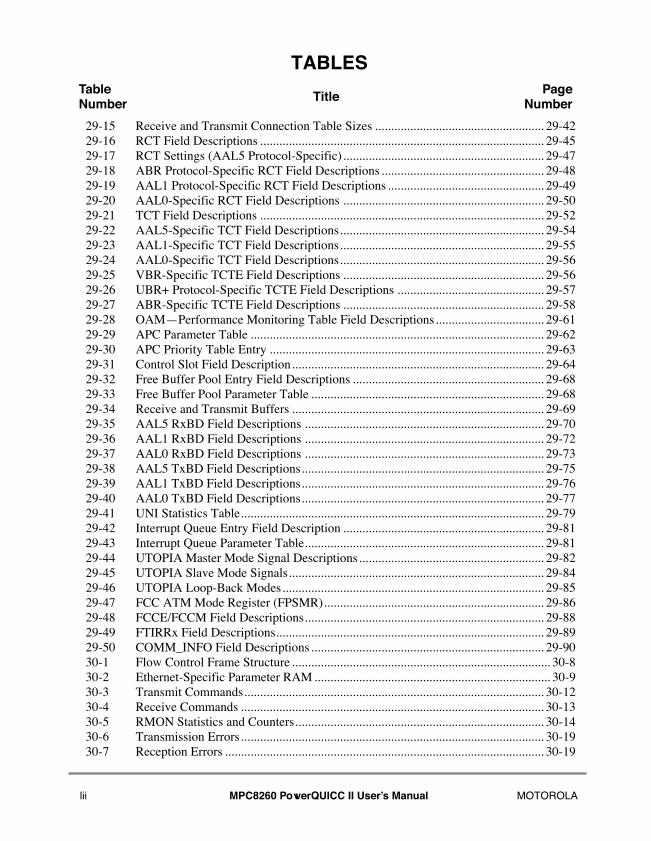
TABLESTableNumber Title Page
Number
29-15 Receive and Transmit Connection Table Sizes ..................................................... 29-4229-16 RCT Field Descriptions ......................................................................................... 29-4529-17 RCT Settings (AAL5 Protocol-Specific)............................................................... 29-4729-18 ABR Protocol-Specific RCT Field Descriptions ................................................... 29-4829-19 AAL1 Protocol-Specific RCT Field Descriptions ................................................. 29-4929-20 AAL0-Specific RCT Field Descriptions ............................................................... 29-5029-21 TCT Field Descriptions ......................................................................................... 29-5229-22 AAL5-Specific TCT Field Descriptions................................................................ 29-5429-23 AAL1-Specific TCT Field Descriptions................................................................ 29-5529-24 AAL0-Specific TCT Field Descriptions................................................................ 29-5629-25 VBR-Specific TCTE Field Descriptions ............................................................... 29-5629-26 UBR+ Protocol-Specific TCTE Field Descriptions .............................................. 29-5729-27 ABR-Specific TCTE Field Descriptions ............................................................... 29-5829-28 OAMÑPerformance Monitoring Table Field Descriptions.................................. 29-6129-29 APC Parameter Table ............................................................................................ 29-6229-30 APC Priority Table Entry ...................................................................................... 29-6329-31 Control Slot Field Description............................................................................... 29-6429-32 Free Buffer Pool Entry Field Descriptions ............................................................ 29-6829-33 Free Buffer Pool Parameter Table ......................................................................... 29-6829-34 Receive and Transmit Buffers ............................................................................... 29-6929-35 AAL5 RxBD Field Descriptions ........................................................................... 29-7029-36 AAL1 RxBD Field Descriptions ........................................................................... 29-7229-37 AAL0 RxBD Field Descriptions ........................................................................... 29-7329-38 AAL5 TxBD Field Descriptions............................................................................ 29-7529-39 AAL1 TxBD Field Descriptions............................................................................ 29-7629-40 AAL0 TxBD Field Descriptions............................................................................ 29-7729-41 UNI Statistics Table............................................................................................... 29-7929-42 Interrupt Queue Entry Field Description ............................................................... 29-8129-43 Interrupt Queue Parameter Table........................................................................... 29-8129-44 UTOPIA Master Mode Signal Descriptions.......................................................... 29-8229-45 UTOPIA Slave Mode Signals................................................................................ 29-8429-46 UTOPIA Loop-Back Modes.................................................................................. 29-8529-47 FCC ATM Mode Register (FPSMR)..................................................................... 29-8629-48 FCCE/FCCM Field Descriptions........................................................................... 29-8829-49 FTIRRx Field Descriptions.................................................................................... 29-8929-50 COMM_INFO Field Descriptions......................................................................... 29-9030-1 Flow Control Frame Structure ................................................................................. 30-830-2 Ethernet-Specific Parameter RAM .......................................................................... 30-930-3 Transmit Commands.............................................................................................. 30-1230-4 Receive Commands ............................................................................................... 30-1330-5 RMON Statistics and Counters.............................................................................. 30-1430-6 Transmission Errors............................................................................................... 30-1930-7 Reception Errors .................................................................................................... 30-19
lii MPC8260 PowerQUICC II UserÕs Manual MOTOROLA
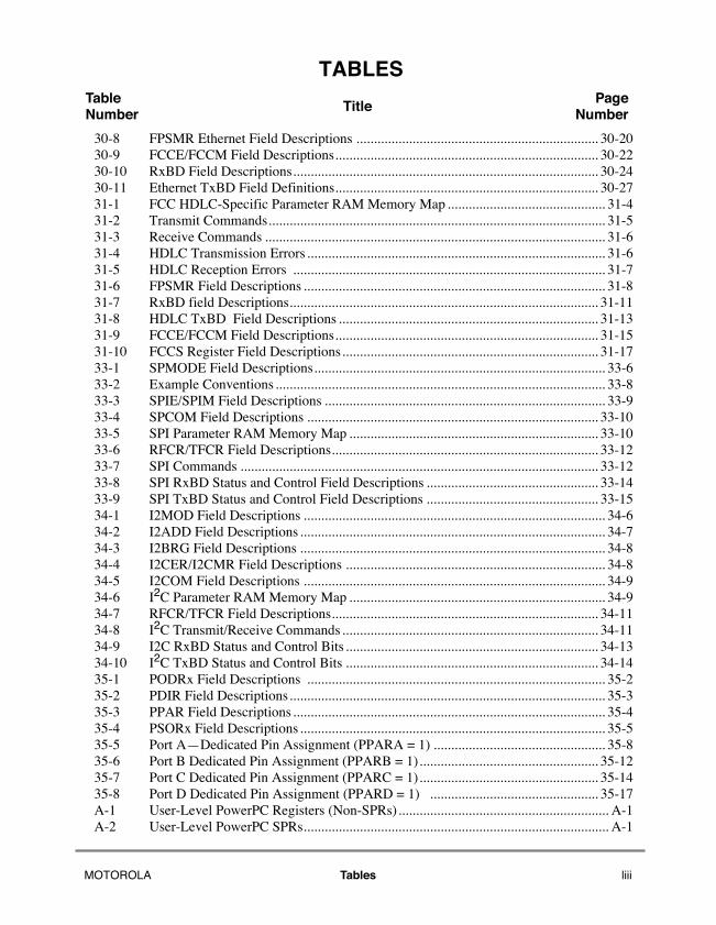
TABLESTableNumber Title Page
Number
30-8 FPSMR Ethernet Field Descriptions ..................................................................... 30-2030-9 FCCE/FCCM Field Descriptions........................................................................... 30-2230-10 RxBD Field Descriptions....................................................................................... 30-2430-11 Ethernet TxBD Field Definitions........................................................................... 30-2731-1 FCC HDLC-Specific Parameter RAM Memory Map ............................................. 31-431-2 Transmit Commands................................................................................................ 31-531-3 Receive Commands ................................................................................................. 31-631-4 HDLC Transmission Errors ..................................................................................... 31-631-5 HDLC Reception Errors ......................................................................................... 31-731-6 FPSMR Field Descriptions ...................................................................................... 31-831-7 RxBD field Descriptions........................................................................................ 31-1131-8 HDLC TxBD Field Descriptions .......................................................................... 31-1331-9 FCCE/FCCM Field Descriptions........................................................................... 31-1531-10 FCCS Register Field Descriptions......................................................................... 31-1733-1 SPMODE Field Descriptions................................................................................... 33-633-2 Example Conventions.............................................................................................. 33-833-3 SPIE/SPIM Field Descriptions ................................................................................ 33-933-4 SPCOM Field Descriptions ................................................................................... 33-1033-5 SPI Parameter RAM Memory Map ....................................................................... 33-1033-6 RFCR/TFCR Field Descriptions............................................................................ 33-1233-7 SPI Commands ...................................................................................................... 33-1233-8 SPI RxBD Status and Control Field Descriptions ................................................. 33-1433-9 SPI TxBD Status and Control Field Descriptions ................................................. 33-1534-1 I2MOD Field Descriptions ...................................................................................... 34-634-2 I2ADD Field Descriptions....................................................................................... 34-734-3 I2BRG Field Descriptions ....................................................................................... 34-834-4 I2CER/I2CMR Field Descriptions .......................................................................... 34-834-5 I2COM Field Descriptions ...................................................................................... 34-934-6 I2C Parameter RAM Memory Map ......................................................................... 34-934-7 RFCR/TFCR Field Descriptions............................................................................ 34-1134-8 I2C Transmit/Receive Commands......................................................................... 34-1134-9 I2C RxBD Status and Control Bits ........................................................................ 34-1334-10 I2C TxBD Status and Control Bits ........................................................................ 34-1435-1 PODRx Field Descriptions ..................................................................................... 35-235-2 PDIR Field Descriptions.......................................................................................... 35-335-3 PPAR Field Descriptions......................................................................................... 35-435-4 PSORx Field Descriptions....................................................................................... 35-535-5 Port AÑDedicated Pin Assignment (PPARA = 1) ................................................. 35-835-6 Port B Dedicated Pin Assignment (PPARB = 1)................................................... 35-1235-7 Port C Dedicated Pin Assignment (PPARC = 1)................................................... 35-1435-8 Port D Dedicated Pin Assignment (PPARD = 1) ................................................ 35-17A-1 User-Level PowerPC Registers (Non-SPRs)............................................................ A-1A-2 User-Level PowerPC SPRs....................................................................................... A-1
MOTOROLA Tables liii
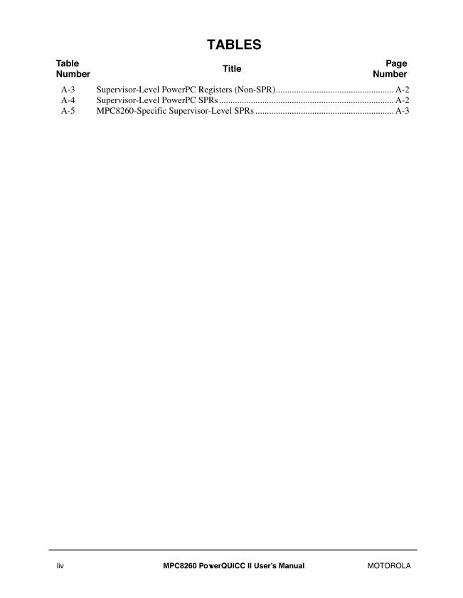
TABLESTableNumber Title Page
Number
A-3 Supervisor-Level PowerPC Registers (Non-SPR).................................................... A-2A-4 Supervisor-Level PowerPC SPRs............................................................................. A-2A-5 MPC8260-Specific Supervisor-Level SPRs ............................................................. A-3
liv MPC8260 PowerQUICC II UserÕs Manual MOTOROLA
About This BookThe primary objective of this manual is to help communications system designers buildsystems using the Motorola MPC8260 and to help software designers provide operatingsystems and user-level applications to take fullest advantage of the MPC8260.
Although this book describes aspects regarding the PowerPCª architecture that are criticalfor understanding the MPC8260 core, it does not contain a complete description of thearchitecture. Where additional information might help the reader, references are made toThe PowerPC Microprocessor Family: The Programming Environments. Orderinginformation for this book are provided in the section, ÒPowerPC Documentation.Ó
The information in this book is subject to change without notice, as described in thedisclaimers on the title page of this book. As with any technical documentation, it is thereadersÕ responsibility to be sure they are using the most recent version of thedocumentation. For more information, contact your sales representative.
Before Using this ManualÑImportant NoteBefore using this manual, determine whether it is the latest revision and if there are errataor addenda. To locate any published errata or updates for this document, refer to the world-wide web at http://www.motorola.com/netcomm.
AudienceThis manual is intended for software and hardware developers and applicationprogrammers who want to develop products for the MPC8260. It is assumed that the readerhas a basic understanding of computer networking, OSI layers, and RISC architecture. Inaddition, it is assumed that the reader has a basic understanding of the communicationsprotocols described here. Where it is considered useful, additional sources are provided thatprovide in-depth discussions of such topics.
MOTOROLA About This Book lv
OrganizationFollowing is a summary and a brief description of the chapters of this manual:
¥ Part I, ÒOverview,Ó provides a high-level description of the MPC8260, describing general operation and listing basic features.
Ñ Chapter 1, ÒOverview,Ó provides a high-level description of MPC8260 functions and features. It roughly follows the structure of this book, summarizing the relevant features and providing references for the reader who needs additional information.
Ñ Chapter 2, ÒPowerPC Processor Core,Ó provides an overview of the MPC8260 core, summarizing topics described in further detail in subsequent chapters.
Ñ Chapter 3, ÒMemory Map,Ó presents a table showing where MPC8260 registers are mapped in memory. It includes cross references that indicate where the registers are described in detail.
¥ Part II, ÒConÞguration and Reset,Ó describes start-up behavior of the MPC8260
Ñ Chapter 4, ÒSystem Interface Unit (SIU),Ó describes the system conÞguration and protection functions which provide various monitors and timers, and the 60x bus conÞguration.
Ñ Chapter 5, ÒReset,Ó describes the behavior of the MPC8260 at reset and start-up.
¥ Part III, ÒThe Hardware Interface,Ó describes external signals, clocking, memory control, and power management of the MPC8260.
Ñ Chapter 6, ÒExternal Signals,Ó shows a functional pinout of the MPC8260 and describes the MPC8260 signals.
Ñ Chapter 7, Ò60x Signals,Ó describes signals on the 60x bus.
Ñ Chapter 8, ÒThe 60x Bus,Ó describes the operation of the bus used by PowerPC processors.
Ñ Chapter 9, ÒClocks and Power Control,Ó describes the clocking architecture of the MPC8260.
Ñ Chapter 10, ÒMemory Controller,Ó describes the memory controller, which controlling a maximum of eight memory banks shared between a general-purpose chip-select machine (GPCM) and three user-programmable machines (UPMs).
Ñ Chapter 11, ÒSecondary (L2) Cache Support,Ó provides information about implementation and conÞguration of a level-2 cache.
Ñ Chapter 12, ÒIEEE 1149.1 Test Access Port,Ó describes the dedicated user-accessible test access port (TAP), which is fully compatible with the IEEE 1149.1 Standard Test Access Port and Boundary Scan Architecture.
¥ Part IV, ÒCommunications Processor Module,Ó describes the conÞguration, clocking, and operation of the various communications protocols supported by the MPC8260.
lvi MPC8260 PowerQUICC II UserÕs Manual MOTOROLA
Ñ Chapter 13, ÒCommunications Processor Module Overview,Ó provides a brief overview of the MPC8260 CPM.
Ñ Chapter 14, ÒSerial Interface with Time-Slot Assigner,Ó describes the SIU, which controls system start-up, initialization and operation, protection, as well as the external system bus.
Ñ Chapter 15, ÒCPM Multiplexing,Ó describes the CPM multiplexing logic (CMX) which connects the physical layerÑUTOPIA, MII, modem lines,
Ñ Chapter 16, ÒBaud-Rate Generators (BRGs),Ó describes the eight independent, identical baud-rate generators (BRGs) that can be used with the FCCs, SCCs, and SMCs.
Ñ Chapter 17, ÒTimers,Ó describes the MPC8260 timer implementation, which can be conÞgured as four identical 16-bit or two 32-bit general-purpose timers.
Ñ Chapter 18, ÒSDMA Channels and IDMA Emulation,Ó describes the two physical serial DMA (SDMA) channels on the MPC8260.
Ñ Chapter 19, ÒSerial Communications Controllers (SCCs),Ó describes the four serial communications controllers (SCC), which can be conÞgured independently to implement different protocols for bridging functions, routers, and gateways, and to interface with a wide variety of standard WANs, LANs, and proprietary networks.
Ñ Chapter 20, ÒSCC UART Mode,Ó describes the MPC8260 implementation of universal asynchronous receiver transmitter (UART) protocol that is used for sending low-speed data between devices.
Ñ Chapter 21, ÒSCC HDLC Mode,Ó describes the MPC8260 implementation of HDLC protocol.
Ñ Chapter 22, ÒSCC BISYNC Mode,Ó describes the MPC8260 implementation of byte-oriented BISYNC protocol developed by IBM for use in networking products.
Ñ Chapter 23, ÒSCC Transparent Mode,Ó describes the MPC8260 implementation of transparent mode (also called totally transparent mode), which provides a clear channel on which the SCC can send or receive serial data without bit-level manipulation.
Ñ Chapter 24, ÒSCC Ethernet Mode,Ó describes the MPC8260 implementation of Ethernet protocol.
Ñ Chapter 25, ÒSCC AppleTalk Mode,Ó describes the MPC8260 implementation of AppleTalk.
Ñ Chapter 26, ÒSerial Management Controllers (SMCs),Ó describes two serial management controllers, full-duplex ports that can be conÞgured independently to support one of three protocolsÑUART, transparent, or general-circuit interface (GCI).
MOTOROLA About This Book lvii
Ñ Chapter 27, ÒMulti-Channel Controllers (MCCs),Ó describes the MPC8260Õs multi-channel controller (MCC), which handles up to 128 serial, full-duplex data channels.
Ñ Chapter 28, ÒFast Communications Controllers (FCCs),Ó describes the MPC8260Õs fast communications controllers (FCCs), which are SCCs optimized for synchronous high-rate protocols.
Ñ Chapter 29, ÒATM Controller,Ó describes the MPC8260 ATM controller, which provides the ATM and AAL layers of the ATM protocol. The ATM controller performs segmentation and reassembly (SAR) functions of AAL5, AAL1, and AAL0, and most of the common parts convergence sublayer (CP-CS) of these protocols.
Ñ Chapter 30, ÒFast Ethernet Controller,Ó describes the MPC8260Õs implementation of the Ethernet IEEE 802.3 protocol.
Ñ Chapter 31, ÒFCC HDLC Controller,Ó describes the FCC implementation of the HDLC protocol.
Ñ Chapter 32, ÒFCC Transparent Controller,Ó describes the FCC implementation of the transparent protocol.
Ñ Chapter 33, ÒSerial Peripheral Interface (SPI),Ó describes the serial peripheral interface, which allows the MPC8260 to exchange data between other MPC8260 chips, the MC68360, the MC68302, the M68HC11, and M68HC05 microcontroller families, and peripheral devices such as EEPROMs, real-time clocks, A/D converters, and ISDN devices.
Ñ Chapter 34, ÒI2C Controller,Ó describes the MPC8260 implementation of the inter-integrated circuit (I2C¨) controller, which allows data to be exchanged with other I2C devices, such as microcontrollers, EEPROMs, real-time clock devices, and A/D converters.
Ñ Chapter 35, ÒParallel I/O Ports,Ó describes the four general-purpose I/O ports AÐD. Each signal in the I/O ports can be conÞgured as a general-purpose I/O signal or as a signal dedicated to supporting communications devices, such as SMCs, SCCs. MCCs, and FCCs.
¥ Appendix A, ÒRegister Quick Reference Guide,Ó provides a quick reference to the registers incorporated in the PowerPC core.
¥ This book also includes an index and a glossary.
lviii MPC8260 PowerQUICC II UserÕs Manual MOTOROLA

Suggested ReadingThis section lists additional reading that provides background for the information in thismanual as well as general information about the PowerPC architecture.
MPC8xx DocumentationSupporting documentation for the MPC8260 can be accessed through the world-wide webat http://www.mot.com/netcomm. This documentation includes technical speciÞcations,reference materials, and detailed applications notes.
PowerPC DocumentationThe PowerPC documentation is organized in the following types of documents:
¥ UserÕs manualsÑThese books provide details about individual PowerPC implementations and are intended to be used in conjunction with The Programming Environments Manual. These include the following:
Ñ PowerPC MPC603eª & EC603e RISC Microprocessor UserÕs Manual (Motorola order #: MPC603EUM/AD, Rev. 1)
Ñ PowerPC 604ª RISC Microprocessor UserÕs Manual(Motorola order #: MPC604UM/AD)
¥ Programming environments manualsÑThese books provide information about resources deÞned by the PowerPC architecture that are common to PowerPC processors. There are two versions, one that describes the functionality of the combined 32- and 64-bit architecture models and one that describes only the 32-bit model.
Ñ PowerPC Microprocessor Family: The Programming Environments, Rev 1 (Motorola order #: MPCFPE/AD)
Ñ PowerPC Microprocessor Family: The Programming Environments for 32-Bit Microprocessors, Rev. 1 (Motorola order #: MPCFPE32B/AD)
¥ PowerPC Microprocessor Family: The Bus Interface for 32-Bit Microprocessors (Motorola order #: MPCBUSIF/AD) provides a detailed functional description of the 60x bus interface, as implemented on the PowerPC MPC601ª, MPC603e, MPC604, and MPC750 family of PowerPC microprocessors. This document is intended to help system and chip set developers by providing a centralized reference source to identify the bus interface presented by the 60x family of PowerPC microprocessors.
¥ PowerPC Microprocessor Family: The ProgrammerÕs Reference Guide (Motorola order #: MPCPRG/D) is a concise reference that includes the register summary, memory control model, exception vectors, and the PowerPC instruction set.
¥ PowerPC Microprocessor Family: The ProgrammerÕs Pocket Reference Guide (Motorola order #: MPCPRGREF/D). This feedlot card provides an overview of the PowerPC registers, instructions, and exceptions for 32-bit implementations.
MOTOROLA About This Book lix
¥ Application notesÑThese short documents contain useful information about speciÞc design issues useful to programmers and engineers working with PowerPC processors.
For a current list of PowerPC documentation, refer to the world-wide web athttp://www.mot.com/PowerPC.
ConventionsThis document uses the following notational conventions:
Bold entries in Þgures and tables showing registers and parameter RAM should be initialized by the user.
mnemonics Instruction mnemonics are shown in lowercase bold.
italics Italics indicate variable command parameters, for example, bcctrx.Book titles in text are set in italics.
0x0 PreÞx to denote hexadecimal number
0b0 PreÞx to denote binary number
rA, rB Instruction syntax used to identify a source GPR
rD Instruction syntax used to identify a destination GPR
REG[FIELD] Abbreviations or acronyms for registers or buffer descriptors are shown in uppercase text. SpeciÞc bits, Þelds, or numerical ranges appear in brackets. For example, MSR[LE] refers to the little-endian mode enable bit in the machine state register.
x In certain contexts, such as in a signal encoding or a bit Þeld, indicates a donÕt care.
n Used to express an undeÞned numerical value
 NOT logical operator
& AND logical operator
| OR logical operator
Bold
lx MPC8260 PowerQUICC II UserÕs Manual MOTOROLA
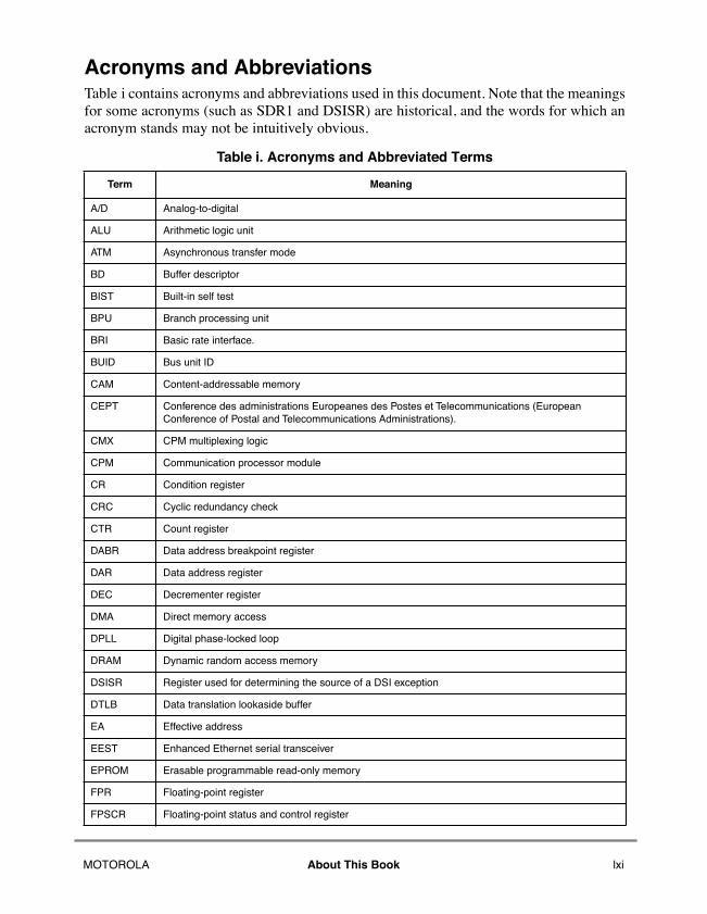
Acronyms and AbbreviationsTable i contains acronyms and abbreviations used in this document. Note that the meaningsfor some acronyms (such as SDR1 and DSISR) are historical, and the words for which anacronym stands may not be intuitively obvious.
Table i. Acronyms and Abbreviated Terms
Term Meaning
A/D Analog-to-digital
ALU Arithmetic logic unit
ATM Asynchronous transfer mode
BD Buffer descriptor
BIST Built-in self test
BPU Branch processing unit
BRI Basic rate interface.
BUID Bus unit ID
CAM Content-addressable memory
CEPT Conference des administrations Europeanes des Postes et Telecommunications (European Conference of Postal and Telecommunications Administrations).
CMX CPM multiplexing logic
CPM Communication processor module
CR Condition register
CRC Cyclic redundancy check
CTR Count register
DABR Data address breakpoint register
DAR Data address register
DEC Decrementer register
DMA Direct memory access
DPLL Digital phase-locked loop
DRAM Dynamic random access memory
DSISR Register used for determining the source of a DSI exception
DTLB Data translation lookaside buffer
EA Effective address
EEST Enhanced Ethernet serial transceiver
EPROM Erasable programmable read-only memory
FPR Floating-point register
FPSCR Floating-point status and control register
MOTOROLA About This Book lxi
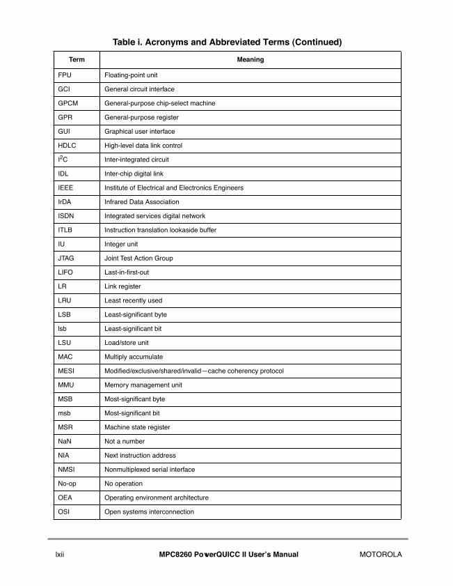
FPU Floating-point unit
GCI General circuit interface
GPCM General-purpose chip-select machine
GPR General-purpose register
GUI Graphical user interface
HDLC High-level data link control
I2C Inter-integrated circuit
IDL Inter-chip digital link
IEEE Institute of Electrical and Electronics Engineers
IrDA Infrared Data Association
ISDN Integrated services digital network
ITLB Instruction translation lookaside buffer
IU Integer unit
JTAG Joint Test Action Group
LIFO Last-in-Þrst-out
LR Link register
LRU Least recently used
LSB Least-signiÞcant byte
lsb Least-signiÞcant bit
LSU Load/store unit
MAC Multiply accumulate
MESI ModiÞed/exclusive/shared/invalidÑcache coherency protocol
MMU Memory management unit
MSB Most-signiÞcant byte
msb Most-signiÞcant bit
MSR Machine state register
NaN Not a number
NIA Next instruction address
NMSI Nonmultiplexed serial interface
No-op No operation
OEA Operating environment architecture
OSI Open systems interconnection
Table i. Acronyms and Abbreviated Terms (Continued)
Term Meaning
lxii MPC8260 PowerQUICC II UserÕs Manual MOTOROLA
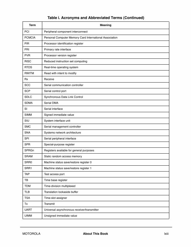
PCI Peripheral component interconnect
PCMCIA Personal Computer Memory Card International Association
PIR Processor identiÞcation register
PRI Primary rate interface
PVR Processor version register
RISC Reduced instruction set computing
RTOS Real-time operating system
RWITM Read with intent to modify
Rx Receive
SCC Serial communication controller
SCP Serial control port
SDLC Synchronous Data Link Control
SDMA Serial DMA
SI Serial interface
SIMM Signed immediate value
SIU System interface unit
SMC Serial management controller
SNA Systems network architecture
SPI Serial peripheral interface
SPR Special-purpose register
SPRGn Registers available for general purposes
SRAM Static random access memory
SRR0 Machine status save/restore register 0
SRR1 Machine status save/restore register 1
TAP Test access port
TB Time base register
TDM Time-division multiplexed
TLB Translation lookaside buffer
TSA Time-slot assigner
Tx Transmit
UART Universal asynchronous receiver/transmitter
UIMM Unsigned immediate value
Table i. Acronyms and Abbreviated Terms (Continued)
Term Meaning
MOTOROLA About This Book lxiii
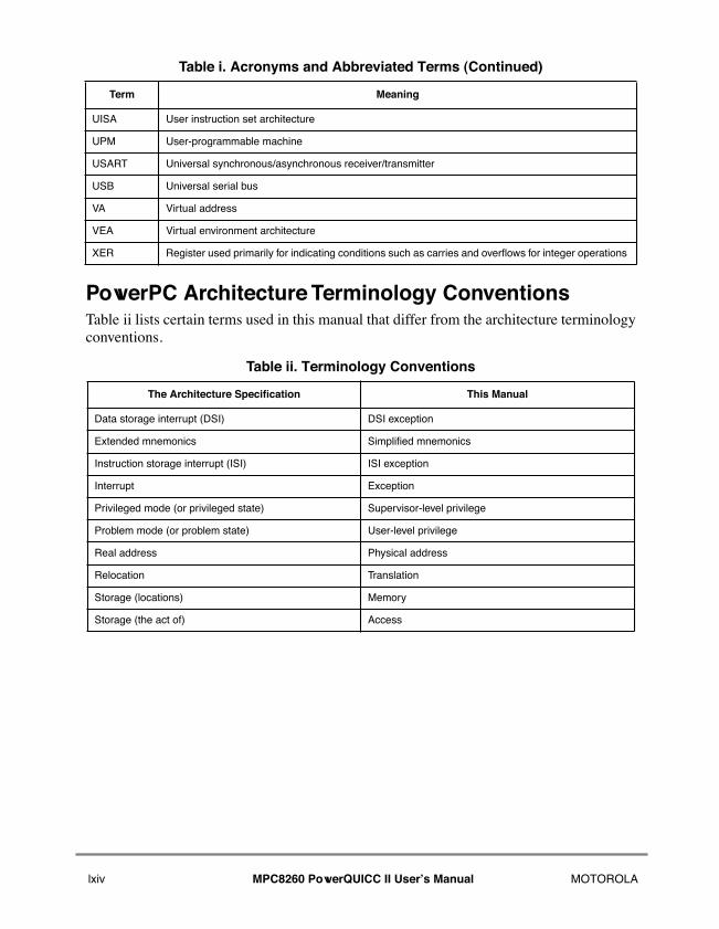
PowerPC Architecture Terminology ConventionsTable ii lists certain terms used in this manual that differ from the architecture terminologyconventions.
UISA User instruction set architecture
UPM User-programmable machine
USART Universal synchronous/asynchronous receiver/transmitter
USB Universal serial bus
VA Virtual address
VEA Virtual environment architecture
XER Register used primarily for indicating conditions such as carries and overßows for integer operations
Table ii. Terminology Conventions
The Architecture SpeciÞcation This Manual
Data storage interrupt (DSI) DSI exception
Extended mnemonics SimpliÞed mnemonics
Instruction storage interrupt (ISI) ISI exception
Interrupt Exception
Privileged mode (or privileged state) Supervisor-level privilege
Problem mode (or problem state) User-level privilege
Real address Physical address
Relocation Translation
Storage (locations) Memory
Storage (the act of) Access
Table i. Acronyms and Abbreviated Terms (Continued)
Term Meaning
lxiv MPC8260 PowerQUICC II UserÕs Manual MOTOROLA
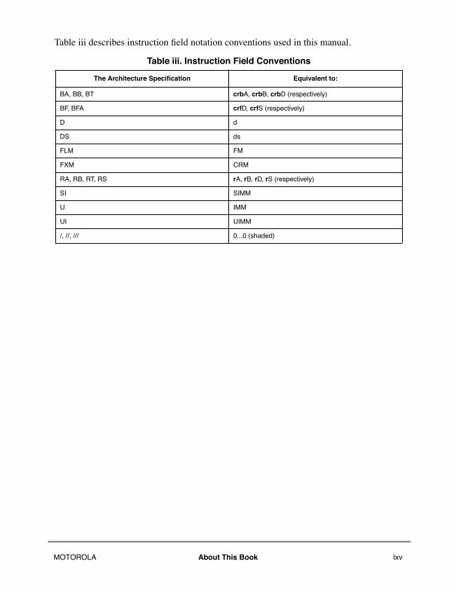
Table iii describes instruction Þeld notation conventions used in this manual.
Table iii. Instruction Field Conventions
The Architecture SpeciÞcation Equivalent to:
BA, BB, BT crbA, crbB, crbD (respectively)
BF, BFA crfD, crfS (respectively)
D d
DS ds
FLM FM
FXM CRM
RA, RB, RT, RS rA, rB, rD, rS (respectively)
SI SIMM
U IMM
UI UIMM
/, //, /// 0...0 (shaded)
MOTOROLA About This Book lxv

lxvi MPC8260 PowerQUICC II UserÕs Manual MOTOROLA
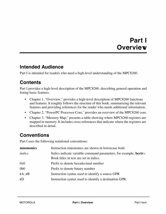
Part IOverview
Intended AudiencePart I is intended for readers who need a high-level understanding of the MPC8260.
ContentsPart I provides a high-level description of the MPC8260, describing general operation andlisting basic features.
¥ Chapter 1, ÒOverview,Ó provides a high-level description of MPC8260 functions and features. It roughly follows the structure of this book, summarizing the relevant features and providing references for the reader who needs additional information.
¥ Chapter 2, ÒPowerPC Processor Core,Ó provides an overview of the MPC8260 core.
¥ Chapter 3, ÒMemory Map,Ó presents a table showing where MPC8260 registers are mapped in memory. It includes cross references that indicate where the registers are described in detail.
ConventionsPart I uses the following notational conventions:
mnemonics Instruction mnemonics are shown in lowercase bold.
italics Italics indicate variable command parameters, for example, bcctrx.Book titles in text are set in italics.
0x0 PreÞx to denote hexadecimal number
0b0 PreÞx to denote binary number
rA, rB Instruction syntax used to identify a source GPR
rD Instruction syntax used to identify a destination GPR
MOTOROLA Part I. Overview Part I-lxvii
Part I. Overview
REG[FIELD] Abbreviations or acronyms for registers or buffer descriptors are shown in uppercase text. SpeciÞc bits, Þelds, or numerical ranges appear in brackets. For example, MSR[LE] refers to the little-endian mode enable bit in the machine state register.
x In certain contexts, such as in a signal encoding or a bit Þeld, indicates a donÕt care.
n Indicates an undeÞned numerical value
Acronyms and AbbreviationsTable iv contains acronyms and abbreviations that are used in this document.
Table iv. Acronyms and Abbreviated Terms
Term Meaning
ATM Asynchronous Mode
BD Buffer descriptor
BPU Branch processing unit
COP Common on-chip processor
CP Communications processor
CPM Communications processor module
CRC Cyclic redundancy check
CTR Count register
DABR Data address breakpoint register
DAR Data address register
DEC Decrementer register
DMA Direct memory access
DPLL Digital phase-locked loop
DRAM Dynamic random access memory
DTLB Data translation lookaside buffer
EA Effective address
FCCÔ Fast communications controller
FPR Floating-point register
GPCM General-purpose chip-select machine
GPR General-purpose register
HDLC High-level data link control
I2C Inter-integrated circuit
IEEE Institute of Electrical and Electronics Engineers
Part I-lxviii MPC8260 PowerQUICC II UserÕs Manual MOTOROLA
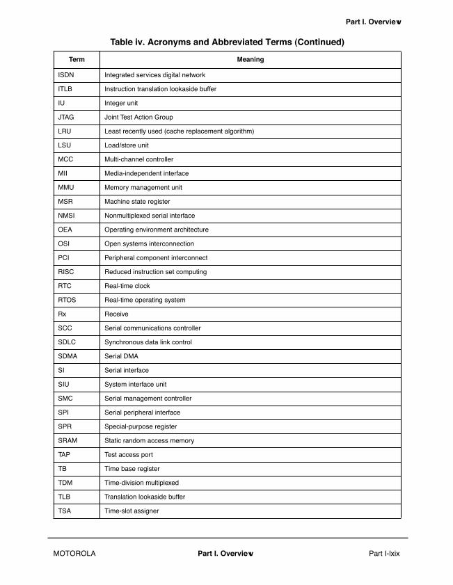
Part I. Overview
ISDN Integrated services digital network
ITLB Instruction translation lookaside buffer
IU Integer unit
JTAG Joint Test Action Group
LRU Least recently used (cache replacement algorithm)
LSU Load/store unit
MCC Multi-channel controller
MII Media-independent interface
MMU Memory management unit
MSR Machine state register
NMSI Nonmultiplexed serial interface
OEA Operating environment architecture
OSI Open systems interconnection
PCI Peripheral component interconnect
RISC Reduced instruction set computing
RTC Real-time clock
RTOS Real-time operating system
Rx Receive
SCC Serial communications controller
SDLC Synchronous data link control
SDMA Serial DMA
SI Serial interface
SIU System interface unit
SMC Serial management controller
SPI Serial peripheral interface
SPR Special-purpose register
SRAM Static random access memory
TAP Test access port
TB Time base register
TDM Time-division multiplexed
TLB Translation lookaside buffer
TSA Time-slot assigner
Table iv. Acronyms and Abbreviated Terms (Continued)
Term Meaning
MOTOROLA Part I. Overview Part I-lxix
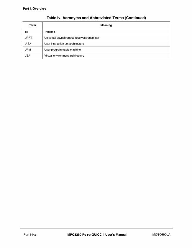
Part I. Overview
Tx Transmit
UART Universal asynchronous receiver/transmitter
UISA User instruction set architecture
UPM User-programmable machine
VEA Virtual environment architecture
Table iv. Acronyms and Abbreviated Terms (Continued)
Term Meaning
Part I-lxx MPC8260 PowerQUICC II UserÕs Manual MOTOROLA
Chapter 1 Overview1010
The MPC8260 PowerQUICC IIª is a versatile communications processor that integrateson one chip a high-performance PowerPCª RISC microprocessor, a very ßexible systemintegration unit, and many communications peripheral controllers that can be used in avariety of applications, particularly in communications and networking systems.
The core is an embedded variant of the PowerPC MPC603eª microprocessor with 16Kbytes of instruction cache and 16 Kbytes of data cache and no ßoating-point unit (FPU).The system interface unit (SIU) consists of a ßexible memory controller that interfaces toalmost any user-deÞned memory system, and many other peripherals making this device acomplete system on a chip.
The communications processor module (CPM) includes all the peripherals found in theMPC860, with the addition of three high-performance communication channels thatsupport new emerging protocols (for example, 155-Mbps ATM and Fast Ethernet).MPC8260 has dedicated hardware that can handle up to 256 full-duplex, time-division-multiplexed logical channels
This document describes the functional operation of MPC8260, with an emphasis onperipheral functions. Chapter 2, ÒPowerPC Processor Core,Ó is an overview of the PowerPCmicroprocessor core; detailed information about the core can be found in the MPC603e &EC603e RISC Microprocessors UserÕs Manual (order number: MPC603EUM/AD).
1.1 FeaturesThe following is an overview of the MPC8260 feature set:
¥ PowerPC dual-issue integer core
Ñ A core version of the MPC603e microprocessor
Ñ System core microprocessor supporting frequencies of 100Ð200 MHz
Ñ Separate 16-Kbyte data and instruction caches:
Ð Four-way set associative
Ð Physically addressed
Ð LRU replacement algorithm
MOTOROLA Chapter 1. Overview 1-1
Part I. Overview
Ñ PowerPC architecture-compliant memory management unit (MMU)
Ñ Common on-chip processor (COP) test interface
Ñ Supports bus snooping for cache coherency
Ñ No ßoating-point unit (FPU). Floating-point arithmetic is not supported.
Ñ Support for ßoating-point loads and stores.
Ñ Support for cache locking.
¥ Low-power (less than 2.5 W when fully operational at 133 MHz, 2-V internal and 3.3-V I/O)
¥ Separate power supply for internal logic (2 V) and for I/O (3.3 V)
¥ Separate PLLs for PowerPC core and for the CPM
Ñ PowerPC core and CPM can run at different frequencies for power/performance optimization
Ñ Internal PowerPC core/bus clock multiplier that provides 1.5:1, 2:1, 2.5:1, 3:1, 3.5:1, 4:1, 5:1, 6:1 ratios
Ñ Internal CPM/bus clock multiplier that provides 2:1, 2.5:1, 3:1, 3.5:1, 4:1, 5:1, 6:1 ratios
¥ 64-bit data and 32-bit address 60x bus
Ñ Bus supports multiple master designs
Ñ Supports single transfers and burst transfers
Ñ 64-, 32-, 16-, and 8-bit port sizes controlled by on-chip memory controller
Ñ Supports data parity or ECC and address parity
¥ 32-bit data and 18-bit address local bus
Ñ Single-master bus, supports external slaves
Ñ Eight-beat burst transfers
Ñ 32-, 16-, and 8-bit port sizes controlled by on-chip memory controller
¥ System interface unit (SIU)
Ñ Clock synthesizer
Ñ Reset controller
Ñ Real-time clock (RTC) register
Ñ Periodic interrupt timer
Ñ Hardware bus monitor and software watchdog timer
Ñ IEEE 1149.1 JTAG test access port
¥ Twelve-bank memory controller
Ñ Glueless interface to SRAM, page mode SDRAM, DRAM, EPROM, Flash and other user-deÞnable peripherals
1-2 MPC8260 PowerQUICC II UserÕs Manual MOTOROLA
Part I. Overview
Ñ Byte write enables and selectable parity generation
Ñ 32-bit address decodes with programmable bank size
Ñ Three user programmable machines, general-purpose chip-select machine, and page mode pipeline SDRAM machine
Ñ Byte selects for 64-bit bus width (60x) and for 32-bit bus width (local)
Ñ Dedicated interface logic for SDRAM
¥ Disable CPU mode
¥ Communications processor module (CPM)
Ñ Embedded 32-bit communications processor (CP) uses a RISC architecture for ßexible support for communications peripherals
Ñ Interfaces to PowerPC core through on-chip 24-Kbyte dual-port RAM and DMA controller
Ñ Serial DMA channels for receive and transmit on all serial channels
Ñ Parallel I/O registers with open-drain and interrupt capability
Ñ Virtual DMA functionality executing memory to memory and memory to I/O transfers
Ñ Three fast communication controllers (FCCs) supporting the following protocols
Ð 10/100-Mbit Ethernet/IEEE 802.3 CDMA/CS interface through media independent interface (MII)
Ð ATMÑfull-duplex SAR at 155 Mbps, UTOPIA interface, AAL5, AAL1, AAL0 protocols, TM 4.0 CBR, VBR, UBR, ABR trafÞc types, up to 64 K external connections
Ð Transparent
Ð HDLCÑup to T3 rates (clear channel)
Ñ Two multichannel controllers (MCCs)
Ð Two 128 serial full-duplex data channels (for a total of 256 64 Kbps channels). Each MCC can be split into four subgroups of 32 channels each.
Ð Almost any combination of subgroups can be multiplexed to single or multiple TDM interfaces
Ñ Four serial communications controllers (SCCs) identical to those on the MPC860, supporting the digital portions of the following protocols:
Ð Ethernet/IEEE 802.3 CDMA/CS
Ð HDLC/SDLC and HDLC bus
Ð Universal asynchronous receiver transmitter (UART)
Ð Synchronous UART
Ð Binary synchronous (BiSync) communications
Ð Transparent
MOTOROLA Chapter 1. Overview 1-3
Part I. Overview
Ñ Two serial management controllers (SMCs), identical to those of the MPC860
Ð Provide management for BRI devices as general-circuit interface (GCI) controllers in time- division-multiplexed (TDM) channels
Ð Transparent
Ð UART (low-speed operation)
Ñ One serial peripheral interface identical to the MPC860 SPI
Ñ One I2C controller (identical to the MPC860 I2C controller)
Ð Microwire compatible
Ð Multiple-master, single-master, and slave modes
Ñ Up to eight TDM interfaces
Ð Supports two groups of four TDM channels for a total of eight TDMs
Ð 2,048 bytes of SI RAM
Ð Bit or byte resolution
Ð Independent transmit and receive routing, frame synchronization.
Ð Supports T1, CEPT, T1/E1, T3/E3, pulse code modulation highway, ISDN basic rate, ISDN primary rate, Motorola interchip digital link (IDL), general circuit interface (GCI), and user-deÞned TDM serial interfaces
Ñ Eight independent baud rate generators and 20 input clock pins for supplying clocks to FCC, SCC, and SMC serial channels
Ñ Four independent 16-bit timers that can be interconnected as two 32-bit timers
1.2 MPC8260Õs Architecture OverviewThe MPC8260 has two external buses to accommodate bandwidth requirements from thehigh-speed system core and the very fast communications channels. As shown inFigure 1-1, the MPC8260 has three major functional blocks:
¥ A 64-bit PowerPC core derived from the MPC603e with MMUs and cache
¥ A system interface unit (SIU)
¥ A communications processor module (CPM)
1-4 MPC8260 PowerQUICC II UserÕs Manual MOTOROLA
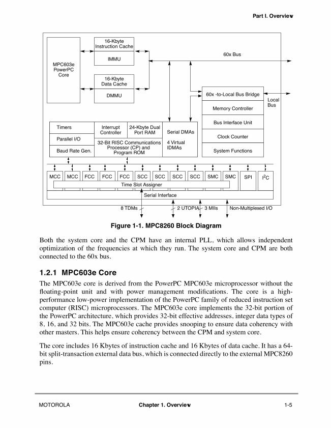
Part I. Overview
Figure 1-1. MPC8260 Block Diagram
Both the system core and the CPM have an internal PLL, which allows independentoptimization of the frequencies at which they run. The system core and CPM are bothconnected to the 60x bus.
1.2.1 MPC603e CoreThe MPC603e core is derived from the PowerPC MPC603e microprocessor without theßoating-point unit and with power management modiÞcations. The core is a high-performance low-power implementation of the PowerPC family of reduced instruction setcomputer (RISC) microprocessors. The MPC603e core implements the 32-bit portion ofthe PowerPC architecture, which provides 32-bit effective addresses, integer data types of8, 16, and 32 bits. The MPC603e cache provides snooping to ensure data coherency withother masters. This helps ensure coherency between the CPM and system core.
The core includes 16 Kbytes of instruction cache and 16 Kbytes of data cache. It has a 64-bit split-transaction external data bus, which is connected directly to the external MPC8260pins.
MPC603ePowerPC
Core
16-KbyteInstruction Cache
IMMU
16-KbyteData Cache
DMMU
60x Bus
LocalBus
60x -to-Local Bus Bridge
Memory Controller
Bus Interface Unit
Clock Counter
System Functions
Timers
Parallel I/O
Baud Rate Gen.
InterruptController
24-Kbyte DualPort RAM
32-Bit RISC CommunicationsProcessor (CP) and
Serial DMAs
4 Virtual IDMAs
MCC MCC FCC FCC FCC SCC SCC SCC SCC SMC SMC SPI I2CTime Slot Assigner
Serial Interface
8 TDMs 2 UTOPIA 3 MIIs Non-Multiplexed I/O
Program ROM
MOTOROLA Chapter 1. Overview 1-5
Part I. Overview
The MPC603e core has an internal common on-chip (COP) debug processor. Thisprocessor allows access to internal scan chains for debugging purposes. It is also used as aserial connection to the core for emulator support.
The MPC603e core performance for the SPEC 95 benchmark for integer operations rangesbetween 4.4 and 5.1 at 200 MHz. In Dhrystone 2.1 MIPS, the MPC603e is 280 MIPS at200 MHz (compared to 86 MIPS of the MPC860 at 66 MHz).
The MPC603e core can be disabled. In this mode, the MPC8260 functions as a slaveperipheral to an external core or to another MPC8260 device with its core enabled.
1.2.2 System Interface Unit (SIU)The SIU consists of the following:
¥ A 60x-compatible parallel system bus conÞgurable to 64-bit data width. The MPC8260 supports 64-, 32-, 16-, and 8-bit port sizes. The MPC8260 internal arbiter arbitrates between internal components that can access the bus (system core, CPM, and one external master). This arbiter can be disabled, and an external arbiter can be used if necessary.
¥ A local (32-bit data, 32-bit internal and 18-bit external address) bus. This bus is used to enhance the operation of the very high-speed communication controllers. Without requiring extensive manipulation by the core, the bus can be used to store connection tables for ATM or buffer descriptors (BDs) for the communication channels or raw data that is transmitted between channels. The local bus is synchronous to the 60x bus and runs at the same frequency.
¥ Memory controller supporting 12 memory banks that can be allocated for either the system or the local bus. The memory controller is an enhanced version of the MPC860 memory controller. It supports three user-programmable machines. Besides all MPC860 features, the memory controller also supports SDRAM with page mode and address data pipeline.
¥ Supports JTAG controller IEEE 1149.1 test access port (TAP).
¥ A bus monitor that prevents 60x bus lock-ups, a real-time clock, a periodic interrupt timer, and other system functions useful in embedded applications.
¥ Glueless interface to L2 cache (MPC2605) and 4-/16-K-entry CAM (MCM69C232/MCM69C432).
1.2.3 Communications Processor Module (CPM)The CPM contains features that allow the MPC8260 to excel in a variety of applicationstargeted mainly for networking and telecommunication markets.
The CPM is a superset of the MPC860 PowerQUICC CPM, with enhancements on the CPperformance and additional hardware and microcode routines that support high bit rateprotocols like ATM (up to 155 Mbps full-duplex) and Fast Ethernet (100-Mbps full-duplex).
1-6 MPC8260 PowerQUICC II UserÕs Manual MOTOROLA
Part I. Overview
The following list summarizes the major features of the CPM:
¥ The CP is an embedded 32-bit RISC controller residing on a separate bus (CPM local bus) from the 60x bus (used by the system core). With this separate bus, the CP does not affect the performance of the PowerPC core. The CP handles the lower layer tasks and DMA control activities, leaving the PowerPC core free to handle higher layer activities. The CP has an instruction set optimized for communications, but can also be used for general-purpose applications, relieving the system core of small often repeated tasks.
¥ Two serial DMA (SDMA) that can do simultaneous transfers, optimized for burst transfers to the 60x bus and to the local bus.
¥ Three full-duplex, serial fast communications controllers (FCCs) supporting ATM (155 Mbps) protocol through UTOPIA2 interface (there are two UTOPIA interfaces on the MPC8260), IEEE 802.3 and Fast Ethernet protocols, HDLC up to E3 rates (45 Mbps) and totally transparent operation. Each FCC can be conÞgured to transmit fully transparent and receive HDLC or vice-versa.
¥ Two multichannel controllers (MCCs) that can handle an aggregate of 256 X 64 Kbps HDLC or transparent channels, multiplexed on up to eight TDM interfaces. The MCC also supports super-channels of rates higher than 64 Kbps and subchanneling of the 64-Kbps channels.
¥ Four full-duplex serial communications controllers (SCCs) supporting IEEE802.3/Ethernet, high- level synchronous data link control, HDLC, local talk, UART, synchronous UART, BISYNC, and transparent.
¥ Two full-duplex serial management controllers (SMC) supporting GCI, UART, and transparent operations
¥ Serial peripheral interface (SPI) and I2C bus controllers
¥ Time-slot assigner (TSA) that supports multiplexing of data from any of the four SCCs, three FCCs, and two SMCs.
1.3 Software Compatibility IssuesAs much as possible, the MPC8260 CPM features were made similar to those of theprevious devices (MPC860). The code ßow ports easily from previous devices to theMPC8260, except for new protocols supported by the MPC8260.
Although many registers are new, most registers retain the old status and event bits, so anunderstanding of the programming models of the MC68360, MPC860, or MPC85015 ishelpful. Note that the MPC8260 initialization code requires changes from the MPC860initialization code (Motorola provides reference code).
1.3.1 SignalsFigure 1-2 shows MPC8260 signals grouped by function. Note that many of these signalsare multiplexed and this Þgure does not indicate how these signals are multiplexed.
MOTOROLA Chapter 1. Overview 1-7
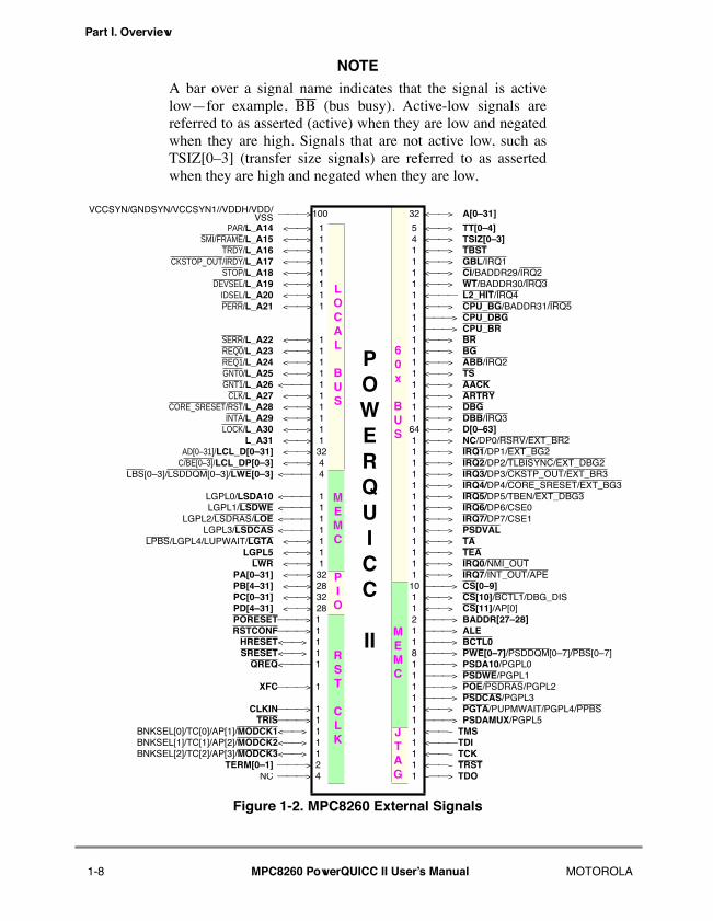
Part I. Overview
NOTEA bar over a signal name indicates that the signal is activelowÑfor example, BB (bus busy). Active-low signals arereferred to as asserted (active) when they are low and negatedwhen they are high. Signals that are not active low, such asTSIZ[0Ð3] (transfer size signals) are referred to as assertedwhen they are high and negated when they are low.
Figure 1-2. MPC8260 External Signals
VCCSYN/GNDSYN/VCCSYN1//VDDH/VDD/VSS ¾¾¾>100
POWERQUICC
II
60x
BUS
32 <¾¾> A[0Ð31]
PAR/L_A14 <¾¾> 1
LOCAL
BUS
5 <¾¾> TT[0Ð4]SMI/FRAME/L_A15 <¾¾> 1 4 <¾¾> TSIZ[0Ð3]
TRDY/L_A16 <¾¾> 1 1 <¾¾> TBSTCKSTOP_OUT/IRDY/L_A17 <¾¾> 1 1 <¾¾> GBL/IRQ1
STOP/L_A18 <¾¾> 1 1 <¾¾> CI/BADDR29/IRQ2DEVSEL/L_A19 <¾¾> 1 1 <¾¾> WT/BADDR30/IRQ3
IDSEL/L_A20 <¾¾> 1 1 <¾¾¾ L2_HIT/IRQ4PERR/L_A21 <¾¾> 1 1 <¾¾> CPU_BG/BADDR31/IRQ5
1 ¾¾¾> CPU_DBG1 ¾¾¾> CPU_BR
SERR/L_A22 <¾¾> 1 1 <¾¾> BRREQ0/L_A23 <¾¾> 1 1 <¾¾> BGREQ1/L_A24 <¾¾> 1 1 <¾¾> ABB/IRQ2GNT0/L_A25 <¾¾> 1 1 <¾¾> TSGNT1/L_A26 <¾¾¾ 1 1 <¾¾> AACK
CLK/L_A27 <¾¾> 1 1 <¾¾> ARTRYCORE_SRESET/RST/L_A28 <¾¾> 1 1 <¾¾> DBG
INTA/L_A29 <¾¾> 1 1 <¾¾> DBB/IRQ3LOCK/L_A30 <¾¾> 1 64 <¾¾> D[0Ð63]
L_A31 <¾¾> 1 1 <¾¾> NC/DP0/RSRV/EXT_BR2AD[0–31]/LCL_D[0Ð31] <¾¾> 32 1 <¾¾> IRQ1/DP1/EXT_BG2
C/BE[0–3]/LCL_DP[0Ð3] <¾¾> 4 1 <¾¾> IRQ2/DP2/TLBISYNC/EXT_DBG2LBS[0Ð3]/LSDDQM[0Ð3]/LWE[0Ð3] <¾¾¾ 4
MEMC
1 <¾¾> IRQ3/DP3/CKSTP_OUT/EXT_BR31 <¾¾> IRQ4/DP4/CORE_SRESET/EXT_BG3
LGPL0/LSDA10 <¾¾¾ 1 1 <¾¾> IRQ5/DP5/TBEN/EXT_DBG3LGPL1/LSDWE <¾¾¾ 1 1 <¾¾> IRQ6/DP6/CSE0
LGPL2/LSDRAS/LOE <¾¾¾ 1 1 <¾¾> IRQ7/DP7/CSE1LGPL3/LSDCAS <¾¾¾ 1 1 <¾¾> PSDVAL
LPBS/LGPL4/LUPWAIT/LGTA <¾¾> 1 1 <¾¾> TALGPL5 <¾¾> 1 1 <¾¾> TEA
LWR <¾¾> 1 1 <¾¾> IRQ0/NMI_OUTPA[0Ð31] <¾¾> 32 P
IO
1 <¾¾> IRQ7/INT_OUT/APEPB[4Ð31] <¾¾> 28
MEMC
10 ¾¾¾> CS[0Ð9]PC[0Ð31] <¾¾> 32 1 <¾¾> CS[10]/BCTL1/DBG_DISPD[4Ð31] <¾¾> 28 1 <¾¾> CS[11]/AP[0]PORESET¾¾¾> 1
RST
CLK
2 ¾¾¾> BADDR[27Ð28]RSTCONF¾¾¾> 1 1 ¾¾¾> ALE
HRESET<¾¾> 1 1 ¾¾¾> BCTL0SRESET<¾¾> 1 8 ¾¾¾> PWE[0Ð7]/PSDDQM[0Ð7]/PBS[0Ð7]
QREQ<¾¾¾ 1 1 ¾¾¾> PSDA10/PGPL01 ¾¾¾> PSDWE/PGPL1
XFC¾¾¾> 1 1 ¾¾¾> POE/PSDRAS/PGPL21 ¾¾¾> PSDCAS/PGPL3
CLKIN¾¾¾> 1 1 <¾¾> PGTA/PUPMWAIT/PGPL4/PPBSTRIS¾¾¾> 1 1 ¾¾¾> PSDAMUX/PGPL5
BNKSEL[0]/TC[0]/AP[1]/MODCK1<¾¾> 1 JTAG
1 <¾¾- TMSBNKSEL[1]/TC[1]/AP[2]/MODCK2<¾¾> 1 1 <¾¾¾TDIBNKSEL[2]/TC[2]/AP[3]/MODCK3<¾¾> 1 1 <¾¾- TCK
TERM[0Ð1] ¾¾¾> 2 1 <¾¾- TRSTNC ¾¾¾> 4 1 -¾¾> TDO
1-8 MPC8260 PowerQUICC II UserÕs Manual MOTOROLA
Part I. Overview
1.4 Differences between MPC860 and MPC8260 The following MPC860 features are not included in the MPC8260.
¥ On-chip crystal oscillators (must use external oscillator)
¥ 4-MHz oscillator (input clock must be at the bus speed)
¥ Low power (stand-by) modes
¥ Battery-backup real-time clock (must use external battery-backup clock)
¥ BDM (COP offers most of the same functionality)
¥ True little-endian mode
¥ PCMCIA interface
¥ Infrared (IR) port
¥ QMC protocol in SCC (256 HDLC channels are supported by the MCCs)
¥ Multiply and accumulate (MAC) block in the CPM
¥ Centronics port (PIP)
¥ Asynchronous HDLC protocol (optional RAM microcode)
¥ Pulse-width modulated outputs
¥ SCC Ethernet controller option to sample 1 byte from the parallel port when a receive frame is complete
¥ Parallel CAM interface for SCC (Ethernet)
1.5 Serial Protocol TableTable 1-1 summarizes available protocols for each serial port.
Table 1-1. MPC8260 Serial Protocols
PortPort
FCC SCC MCC SMC
ATM (Utopia) Ö
100BaseT Ö
10BaseT Ö Ö
HDLC Ö Ö Ö
HDLC_BUS Ö
Transparent Ö Ö Ö Ö
UART Ö Ö
DPLL Ö
Multichannel Ö
MOTOROLA Chapter 1. Overview 1-9
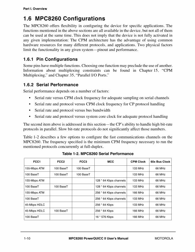
Part I. Overview
1.6 MPC8260 ConÞgurationsThe MPC8260 offers ßexibility in conÞguring the device for speciÞc applications. Thefunctions mentioned in the above sections are all available in the device, but not all of themcan be used at the same time. This does not imply that the device is not fully activated inany given implementation: The CPM architecture has the advantage of using commonhardware resources for many different protocols, and applications. Two physical factorslimit the functionality in any given systemÑpinout and performance.
1.6.1 Pin ConÞgurationsSome pins have multiple functions. Choosing one function may preclude the use of another.Information about multiplexing constraints can be found in Chapter 15, ÒCPMMultiplexing,Ó and Chapter 35, ÒParallel I/O Ports.Ó
1.6.2 Serial PerformanceSerial performance depends on a number of factors:
¥ Serial rate versus CPM clock frequency for adequate sampling on serial channels
¥ Serial rate and protocol versus CPM clock frequency for CP protocol handling
¥ Serial rate and protocol versus bus bandwidth
¥ Serial rate and protocol versus system core clock for adequate protocol handling
The second item above is addressed in this sectionÑthe CPÕs ability to handle high bit-rateprotocols in parallel. Slow bit-rate protocols do not signiÞcantly affect those numbers.
Table 1-2 describes a few options to conÞgure the fast communications channels on theMPC8260. The frequency speciÞed is the minimum CPM frequency necessary to run thementioned protocols concurrently at full-duplex.
Table 1-2. MPC8260 Serial Performance
FCC1 FCC2 FCC3 MCC CPM Clock 60x Bus Clock
155-Mbps ATM 100 BaseT 100 BaseT 133 MHz 66 MHz
100 BaseT 100 BaseT 100 BaseT 133 MHz 66 MHz
155-Mbps ATM 128 * 64 Kbps channels 133 MHz 66 MHz
100 BaseT 100 BaseT 128 * 64 Kbps channels 133 MHz 66 MHz
155-Mbps ATM 256 * 64 Kbps channels 166 MHz 66 MHz
100 BaseT 256 * 64 Kbps channels 133 MHz 66 MHz
45-Mbps HDLC 256 * 64 Kbps 133 MHz 66 MHz
45-Mbps HDLC 100 BaseT 256 * 64 Kbps 166 MHz 66 MHz
100 BaseT 16 * 576 Kbps 166 MHz 66 MHz
1-10 MPC8260 PowerQUICC II UserÕs Manual MOTOROLA
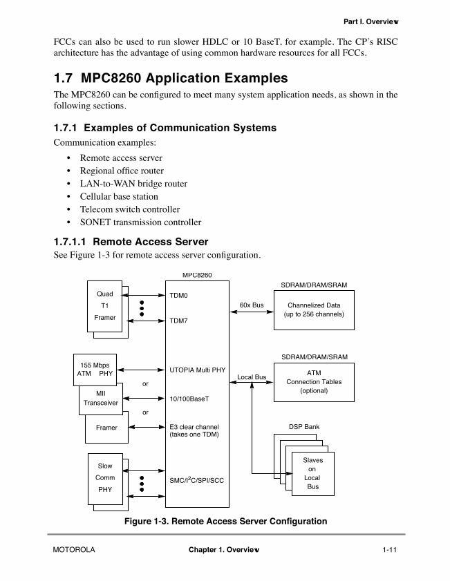
Part I. Overview
FCCs can also be used to run slower HDLC or 10 BaseT, for example. The CPÕs RISCarchitecture has the advantage of using common hardware resources for all FCCs.
1.7 MPC8260 Application Examples The MPC8260 can be conÞgured to meet many system application needs, as shown in thefollowing sections.
1.7.1 Examples of Communication SystemsCommunication examples:
¥ Remote access server¥ Regional ofÞce router¥ LAN-to-WAN bridge router¥ Cellular base station¥ Telecom switch controller¥ SONET transmission controller
1.7.1.1 Remote Access ServerSee Figure 1-3 for remote access server conÞguration.
Figure 1-3. Remote Access Server Configuration
MPC8260
TDM0
TDM7
Quad
T1
Framer
UTOPIA Multi PHY
60x Bus
SDRAM/DRAM/SRAM
Channelized Data
Local Bus
SDRAM/DRAM/SRAM
ATMConnection Tables
(up to 256 channels)
SMC/I2C/SPI/SCC
Slow
Comm
PHY
10/100BaseT
E3 clear channel(takes one TDM)
or
or
Slaves
DSP Bank
on Local Bus
(optional)
Framer
MIITransceiver
155 MbpsPHYATM
MOTOROLA Chapter 1. Overview 1-11
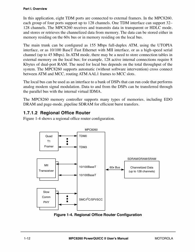
Part I. Overview
In this application, eight TDM ports are connected to external framers. In the MPC8260,each group of four ports support up to 128 channels. One TDM interface can support 32Ð128 channels. The MPC8260 receives and transmits data in transparent or HDLC mode,and stores or retrieves the channelized data from memory. The data can be stored either inmemory residing on the 60x bus or in memory residing on the local bus.
The main trunk can be conÞgured as 155 Mbps full-duplex ATM, using the UTOPIAinterface, or as 10/100 BaseT Fast Ethernet with MII interface, or as a high-speed serialchannel (up to 45 Mbps). In ATM mode, there may be a need to store connection tables inexternal memory on the local bus; for example, 128 active internal connections require 8Kbytes of dual-port RAM. The need for local bus depends on the total throughput of thesystem. The MPC8260 supports automatic (without software intervention) cross connectbetween ATM and MCC, routing ATM AAL1 frames to MCC slots.
The local bus can be used as an interface to a bank of DSPs that can run code that performsanalog modem signal modulation. Data to and from the DSPs can be transferred throughthe parallel bus with the internal virtual IDMA.
The MPC8260 memory controller supports many types of memories, including EDODRAM and page-mode, pipeline SDRAM for efÞcient burst transfers.
1.7.1.2 Regional OfÞce RouterFigure 1-4 shows a regional ofÞce router conÞguration.
Figure 1-4. Regional Office Router Configuration
Quad
T1
Framer
MII
Transceiver
MPC8260
TDM0
TDM3
10/100BaseT 60x Bus
SDRAM/DRAM/SRAM
Channelized Data(up to 128 channels)
10/100BaseT
SMC/I2C/SPI/SCC
Slow
Comm
PHY
1-12 MPC8260 PowerQUICC II UserÕs Manual MOTOROLA
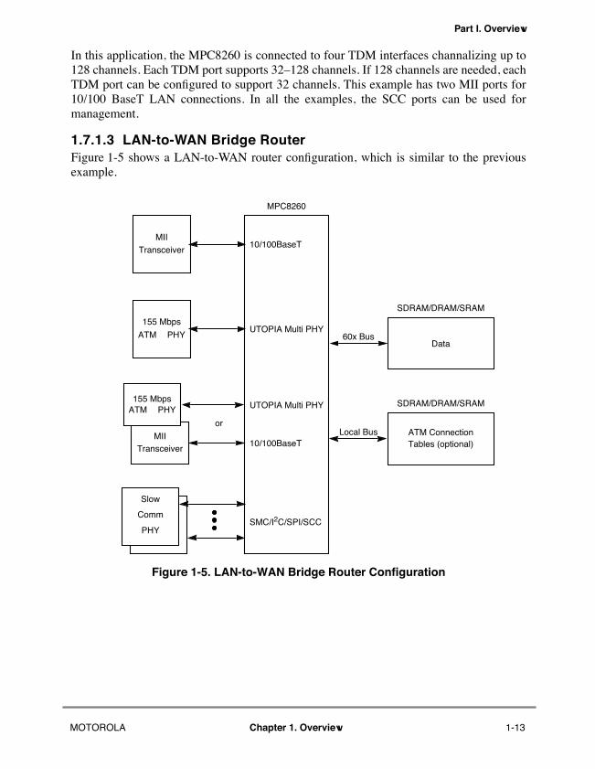
Part I. Overview
In this application, the MPC8260 is connected to four TDM interfaces channalizing up to128 channels. Each TDM port supports 32Ð128 channels. If 128 channels are needed, eachTDM port can be conÞgured to support 32 channels. This example has two MII ports for10/100 BaseT LAN connections. In all the examples, the SCC ports can be used formanagement.
1.7.1.3 LAN-to-WAN Bridge RouterFigure 1-5 shows a LAN-to-WAN router conÞguration, which is similar to the previousexample.
Figure 1-5. LAN-to-WAN Bridge Router Configuration
MPC8260
60x Bus
SDRAM/DRAM/SRAM
Local Bus
SDRAM/DRAM/SRAM
ATM ConnectionTables (optional)
MII
Transceiver10/100BaseT
155 Mbps
PHYATMData
SMC/I2C/SPI/SCC
Slow
Comm
PHY
UTOPIA Multi PHY
10/100BaseT
or
MIITransceiver
155 MbpsPHYATM UTOPIA Multi PHY
MOTOROLA Chapter 1. Overview 1-13
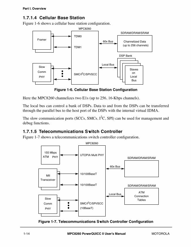
Part I. Overview
1.7.1.4 Cellular Base StationFigure 1-6 shows a cellular base station conÞguration.
Figure 1-6. Cellular Base Station Configuration
Here the MPC8260 channelizes two E1s (up to 256, 16-Kbps channels).
The local bus can control a bank of DSPs. Data to and from the DSPs can be transferredthrough the parallel bus to the host port of the DSPs with the internal virtual IDMA.
The slow communication ports (SCCs, SMCs, I2C, SPI) can be used for management anddebug functions.
1.7.1.5 Telecommunications Switch ControllerFigure 1-7 shows a telecommunications switch controller conÞguration.
Figure 1-7. Telecommunications Switch Controller Configuration
MPC8260
60x Bus
SDRAM/DRAM/SRAM
Channelized Data(up to 256 channels)
DSP Bank
on Local Bus
Local Bus
TDM0
Slaves
SMC/I2C/SPI/SCC
Slow
Comm
PHY
Framer
TDM1
MPC8260
10/100BaseT
60x Bus
SDRAM/DRAM/SRAM
Local Bus
SDRAM/DRAM/SRAM
ATMConnection
Tables
10/100BaseT
SMC/I2C/SPI/SCC
(10BaseT)
UTOPIA Multi PHY
Slow
Comm
PHY
155 Mbps
PHYATM
MII
Transceiver
1-14 MPC8260 PowerQUICC II UserÕs Manual MOTOROLA
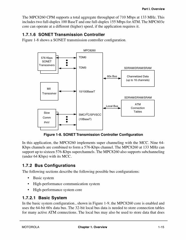
Part I. Overview
The MPC8260 CPM supports a total aggregate throughput of 710 Mbps at 133 MHz. Thisincludes two full-duplex 100 BaseT and one full-duplex 155 Mbps for ATM. The MPC603ecore can operate at a different (higher) speed, if the application requires it.
1.7.1.6 SONET Transmission ControllerFigure 1-8 shows a SONET transmission controller conÞguration.
Figure 1-8. SONET Transmission Controller ConÞguration
In this application, the MPC8260 implements super channeling with the MCC. Nine 64-Kbps channels are combined to form a 576-Kbps channel. The MPC8260 at 133 MHz cansupport up to sixteen 576-Kbps superchannels. The MPC8260 also supports subchanneling(under 64 Kbps) with its MCC.
1.7.2 Bus ConÞgurationsThe following sections describe the following possible bus conÞgurations:
¥ Basic system
¥ High-performance communication system
¥ High-performance system core
1.7.2.1 Basic SystemIn the basic system conÞguration., shown in Figure 1-9, the MPC8260 core is enabled anduses the 64-bit 60x data bus. The 32-bit local bus data is needed to store connection tablesfor many active ATM connections. The local bus may also be used to store data that does
MPC8260
10/100BaseT
60x Bus
SDRAM/DRAM/SRAM
Channelized Data
Local Bus
SDRAM/DRAM/SRAM
ATMConnection
TablesSMC/I2C/SPI/SCC
(10BaseT)
(up to 16 channels)
TDM0
TDM3
MII
Transceiver
576 KbpsSONET
Transceivers
Slow
Comm
PHY
MOTOROLA Chapter 1. Overview 1-15
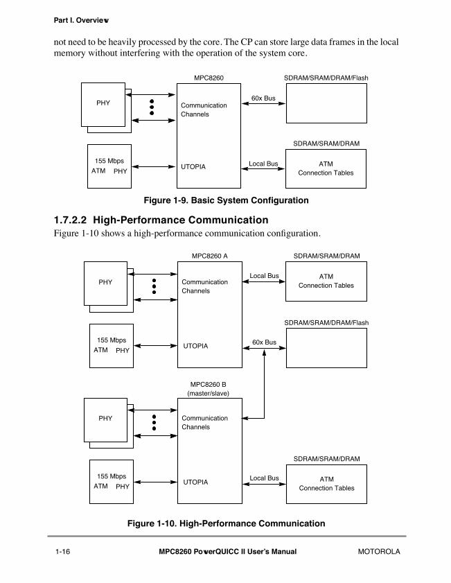
Part I. Overview
not need to be heavily processed by the core. The CP can store large data frames in the localmemory without interfering with the operation of the system core.
Figure 1-9. Basic System Configuration
1.7.2.2 High-Performance CommunicationFigure 1-10 shows a high-performance communication conÞguration.
Figure 1-10. High-Performance Communication
MPC8260
60x Bus
SDRAM/SRAM/DRAM/Flash
Local Bus
SDRAM/SRAM/DRAM
ATMConnection Tables
CommunicationChannels
UTOPIA
PHY
155 Mbps
PHYATM
MPC8260 A
60x Bus
SDRAM/SRAM/DRAM/Flash
Local Bus
SDRAM/SRAM/DRAM
ATMConnection TablesCommunication
Channels
UTOPIA
MPC8260 B
Local Bus
SDRAM/SRAM/DRAM
ATMConnection Tables
(master/slave)
PHY
155 Mbps
PHYATM
CommunicationChannels
UTOPIA
PHY
155 Mbps
PHYATM
1-16 MPC8260 PowerQUICC II UserÕs Manual MOTOROLA
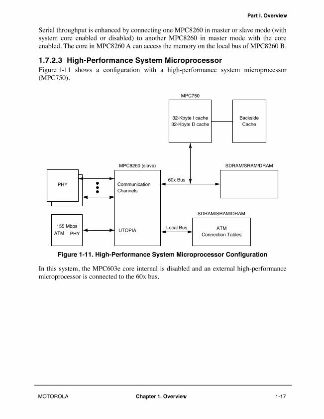
Part I. Overview
Serial throughput is enhanced by connecting one MPC8260 in master or slave mode (withsystem core enabled or disabled) to another MPC8260 in master mode with the coreenabled. The core in MPC8260 A can access the memory on the local bus of MPC8260 B.
1.7.2.3 High-Performance System MicroprocessorFigure 1-11 shows a conÞguration with a high-performance system microprocessor(MPC750).
Figure 1-11. High-Performance System Microprocessor Configuration
In this system, the MPC603e core internal is disabled and an external high-performancemicroprocessor is connected to the 60x bus.
MPC750
32-Kbyte I cache32-Kbyte D cache
BacksideCache
MPC8260 (slave)
Local Bus
SDRAM/SRAM/DRAM
60x Bus
SDRAM/SRAM/DRAM
ATMConnection Tables
CommunicationChannels
UTOPIA
PHY
155 Mbps
PHYATM
MOTOROLA Chapter 1. Overview 1-17

Part I. Overview
1-18 MPC8260 PowerQUICC II UserÕs Manual MOTOROLA
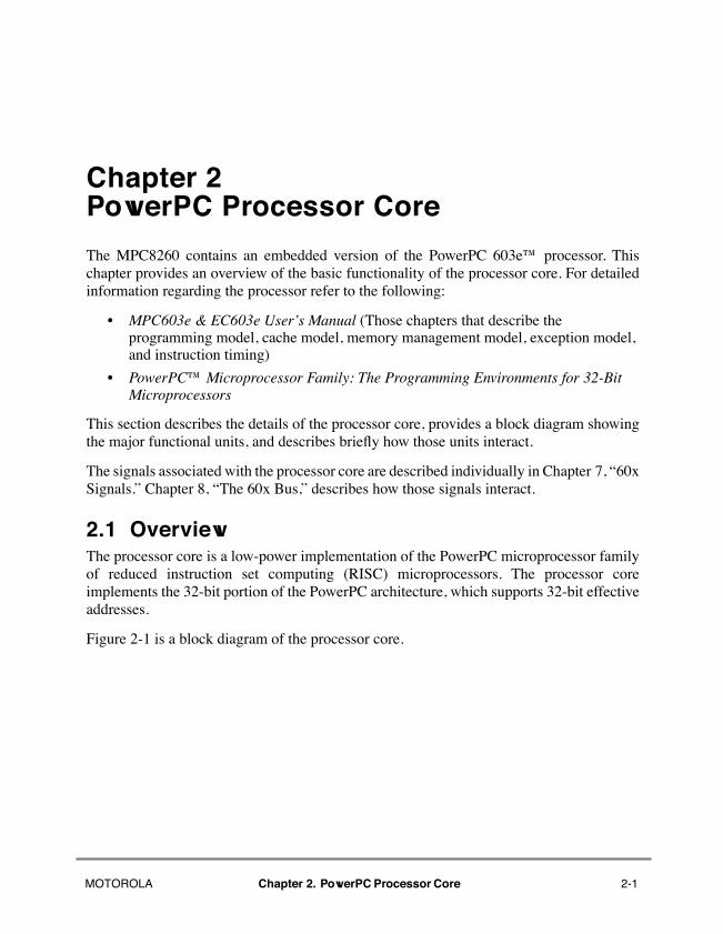
Chapter 2 PowerPC Processor Core2020
The MPC8260 contains an embedded version of the PowerPC 603eª processor. Thischapter provides an overview of the basic functionality of the processor core. For detailedinformation regarding the processor refer to the following:
¥ MPC603e & EC603e UserÕs Manual (Those chapters that describe the programming model, cache model, memory management model, exception model, and instruction timing)
¥ PowerPCª Microprocessor Family: The Programming Environments for 32-Bit Microprocessors
This section describes the details of the processor core, provides a block diagram showingthe major functional units, and describes brießy how those units interact.
The signals associated with the processor core are described individually in Chapter 7, Ò60xSignals.Ó Chapter 8, ÒThe 60x Bus,Ó describes how those signals interact.
2.1 OverviewThe processor core is a low-power implementation of the PowerPC microprocessor familyof reduced instruction set computing (RISC) microprocessors. The processor coreimplements the 32-bit portion of the PowerPC architecture, which supports 32-bit effectiveaddresses.
Figure 2-1 is a block diagram of the processor core.
MOTOROLA Chapter 2. PowerPC Processor Core 2-1
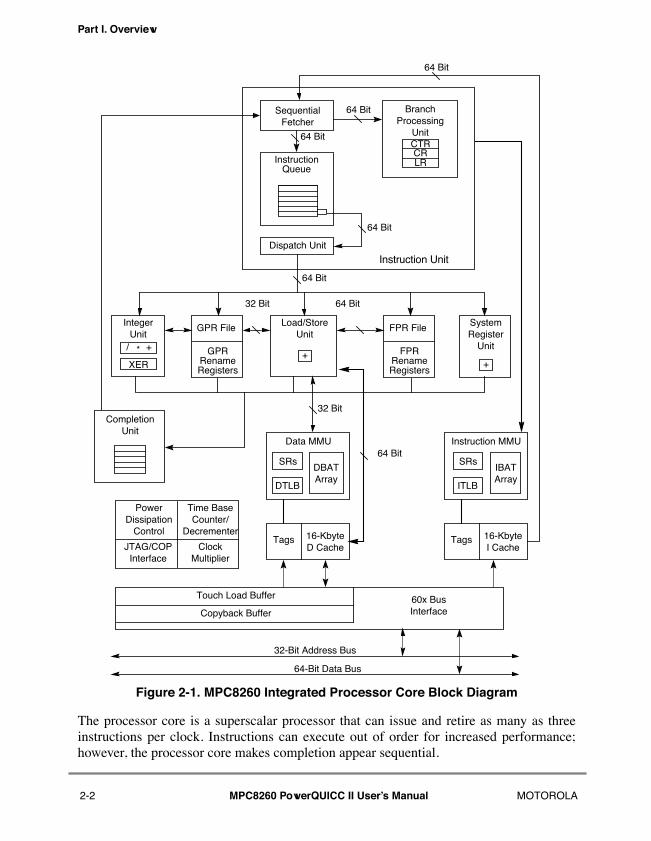
Part I. Overview
Figure 2-1. MPC8260 Integrated Processor Core Block Diagram
The processor core is a superscalar processor that can issue and retire as many as threeinstructions per clock. Instructions can execute out of order for increased performance;however, the processor core makes completion appear sequential.
FPR File
FPRRename Registers
Branch Processing
Unit
Instruction Unit
IntegerUnit
16-KbyteD Cache
Tags
Sequential Fetcher
CTRCRLR
+*/
60x Bus Interface
Data MMU
SRs
DTLB
DBATArray
Touch Load Buffer
Copyback Buffer
64 Bit
32 Bit
Dispatch Unit
64 Bit
Power Dissipation
Control
Completion Unit
Time Base Counter/
Decrementer
ClockMultiplier
JTAG/COPInterface
XER
Instruction MMU
SRs
ITLB
IBATArray
16-KbyteI Cache
Tags
64 Bit
64 Bit
64 Bit
64 Bit32 Bit
GPR File Load/Store Unit
+
64 Bit
GPRRename Registers
InstructionQueue
64-Bit Data Bus
32-Bit Address Bus
SystemRegister
Unit
+
2-2 MPC8260 PowerQUICC II UserÕs Manual MOTOROLA
Part I. Overview
The processor core integrates four execution unitsÑan integer unit (IU), a branchprocessing unit (BPU), a load/store unit (LSU), and a system register unit (SRU). Theability to execute four instructions in parallel and the use of simple instructions with rapidexecution times yield high efÞciency and throughput. Most integer instructions execute inone clock cycle.
The processor core supports integer data types of 8, 16, and 32 bits, and ßoating-point datatypes of 32 and 64 bits. Note that although the MPC8260 does not implement a ßoating-point arithmetic unit, it does retain the 32 architecturally-deÞned ßoating point registers(FPRs), which can be used to hold 32, 64-bit operands that can in turn be transferred to andfrom the 32 general-purpose registers (GPRs), which can hold 32, 32-bit operands.
The processor core provides separate on-chip, 16-Kbyte, four-way set-associative,physically addressed caches for instructions and data and on-chip instruction and datamemory management units (MMUs). The MMUs contain 64-entry, two-way set-associative, data and instruction translation lookaside buffers (DTLB and ITLB) thatprovide support for demand-paged virtual memory address translation and variable-sizedblock translation. The TLBs and caches use a least recently used (LRU) replacementalgorithm. The processor core also supports block address translation through the use oftwo independent instruction and data block address translation (IBAT and DBAT) arrays offour entries each. Effective addresses are compared simultaneously with all four entries inthe BAT array during block translation. In accordance with the PowerPC architecture, if aneffective address hits in both the TLB and BAT array, the BAT translation takes priority.
As an added feature to the MPC603e core, the MPC8260 can lock the contents of 1Ð3 waysin the instruction and data cache (or an entire cache). For example, this allows embeddedapplications to lock interrupt routines or other important (time-sensitive) instructionsequences into the instruction cache. It allows data to be locked into the data cache, whichmay be important to code that must have deterministic execution.
The processor core has a 60x bus that incorporates a 64-bit data bus and a 32-bit addressbus. The processor core supports single-beat and burst data transfers for memory accessesand supports memory-mapped I/O operations.
2.2 PowerPC Processor Core Features
This section describes the major features of the processor core:
¥ High-performance, superscalar microprocessor
Ñ As many as three instructions issued and retired per clock cycle
Ñ As many as four instructions in execution per clock cycle
Ñ Single-cycle execution for most instructions
MOTOROLA Chapter 2. PowerPC Processor Core 2-3
Part I. Overview
¥ Four independent execution units and two register Þles
Ñ BPU featuring static branch predictionÑ A 32-bit IUÑ LSU for data transfer between data cache and GPRs and FPRs Ñ SRU that executes condition register (CR), special-purpose register (SPR), and
integer add/compare instructionsÑ Thirty-two GPRs for integer operandsÑ Thirty-two FPRs. These can be used for operands for ßoating-point load and
store operands, ¥ High instruction and data throughput
Ñ Zero-cycle branch capability (branch folding)Ñ Programmable static branch prediction on unresolved conditional branchesÑ BPU that performs CR lookahead operationsÑ Instruction fetch unit capable of fetching two instructions per clock from the
instruction cacheÑ A six-entry instruction queue that provides lookahead capabilityÑ Independent pipelines with feed-forwarding that reduces data dependencies in
hardwareÑ 16-Kbyte data cacheÑfour-way set-associative, physically addressed; LRU
replacement algorithmÑ 16-Kbyte instruction cacheÑfour-way set-associative, physically addressed;
LRU replacement algorithmÑ Cache write-back or write-through operation programmable on a per page or per
block basisÑ Address translation facilities for 4-Kbyte page size, variable block size, and
256-Mbyte segment size Ñ A 64-entry, two-way set-associative ITLBÑ A 64-entry, two-way set-associative DTLBÑ Four-entry data and instruction BAT arrays providing 128-Kbyte to 256-Mbyte
blocksÑ Software table search operations and updates supported through fast trap
mechanismÑ 52-bit virtual address; 32-bit physical address
¥ Facilities for enhanced system performance
Ñ A 32- or 64-bit, split-transaction external data bus with burst transfersÑ Support for one-level address pipelining and out-of-order bus transactionsÑ Hardware support for misaligned little-endian accessesÑ Added bus multipliers of 4.5x, 5x, 5.5x, 6x, 6.5x 7x, 7.5x, 8x. See Figure 2-3.
2-4 MPC8260 PowerQUICC II UserÕs Manual MOTOROLA
Part I. Overview
¥ Integrated power management
Ñ Three power-saving modes: doze, nap, and sleepÑ Automatic dynamic power reduction when internal functional units are idle
¥ Deterministic behavior and debug features
Ñ On-chip cache locking options for the instruction and data caches (1Ð3 ways or the entire cache contents can be locked)
Ñ In-system testability and debugging features through JTAG and boundary-scan capability
Figure 2-1 shows how the execution unitsÑIU, BPU, LSU, and SRUÑoperateindependently and in parallel. Note that this is a conceptual diagram and does not attemptto show how these features are physically implemented on the chip.
The processor core provides address translation and protection facilities, including anITLB, DTLB, and instruction and data BAT arrays. Instruction fetching and issuing ishandled in the instruction unit. The MMUs translate addresses for cache or externalmemory accesses.
2.2.1 Instruction UnitAs shown in Figure 2-1, the instruction unit, which contains a fetch unit, instruction queue,dispatch unit, and the BPU, provides centralized control of instruction ßow to the executionunits. The instruction unit determines the address of the next instruction to be fetched basedon information from the sequential fetcher and from the BPU.
The instruction unit fetches the instructions from the instruction cache into the instructionqueue. The BPU extracts branch instructions from the fetcher and uses static branchprediction on unresolved conditional branches to allow the instruction unit to fetchinstructions from a predicted target instruction stream while a conditional branch isevaluated. The BPU folds out branch instructions for unconditional branches or conditionalbranches unaffected by instructions in progress in the execution pipeline.
Instructions issued beyond a predicted branch do not complete execution until the branchis resolved, preserving the programming model of sequential execution. If any of theseinstructions are to be executed in the BPU, they are decoded but not issued. Instructions tobe executed by the IU, LSU, and SRU are issued and allowed to complete up to the registerwrite-back stage. Write-back is allowed when a correctly predicted branch is resolved, andinstruction execution continues without interruption on the predicted path. If branchprediction is incorrect, the instruction unit ßushes all predicted path instructions, andinstructions are issued from the correct path.
2.2.2 Instruction Queue and Dispatch UnitThe instruction queue (IQ), shown in Figure 2-1, holds as many as six instructions andloads up to two instructions from the instruction unit during a single cycle. The instructionfetch unit continuously loads as many instructions as space in the IQ allows. Instructions
MOTOROLA Chapter 2. PowerPC Processor Core 2-5
Part I. Overview
are dispatched to their respective execution units from the dispatch unit at a maximum rateof two instructions per cycle. Reservation stations at the IU, LSU, and SRU facilitateinstruction dispatch to those units. The dispatch unit checks for source and destinationregister dependencies, determines dispatch serializations, and inhibits subsequentinstruction dispatching as required. Section 2.7, ÒInstruction Timing,Ó describes instructiondispatch in detail.
2.2.3 Branch Processing Unit (BPU)The BPU receives branch instructions from the fetch unit and performs CR lookaheadoperations on conditional branches to resolve them early, achieving the effect of a zero-cycle branch in many cases.
The BPU uses a bit in the instruction encoding to predict the direction of the conditionalbranch. Therefore, when an unresolved conditional branch instruction is encountered,instructions are fetched from the predicted target stream until the conditional branch isresolved.
The BPU contains an adder to compute branch target addresses and three user-controlregistersÑthe link register (LR), the count register (CTR), and the CR. The BPU calculatesthe return pointer for subroutine calls and saves it into the LR for certain types of branchinstructions. The LR also contains the branch target address for the Branch Conditional toLink Register (bclrx) instruction. The CTR contains the branch target address for theBranch Conditional to Count Register (bcctrx) instruction. The contents of the LR andCTR can be copied to or from any GPR. Because the BPU uses dedicated registers ratherthan GPRs or FPRs, execution of branch instructions is largely independent from executionof other instructions.
2.2.4 Independent Execution UnitsThe PowerPC architectureÕs support for independent execution units allowsimplementation of processors with out-of-order instruction execution. For example,because branch instructions do not depend on GPRs or FPRs, branches can often beresolved early, eliminating stalls caused by taken branches.
In addition to the BPU, the processor core provides three other execution units and acompletion unit, which are described in the following sections.
2.2.4.1 Integer Unit (IU)The IU executes all integer instructions. The IU executes one integer instruction at a time,performing computations with its arithmetic logic unit (ALU), multiplier, divider, and XERregister. Most integer instructions are single-cycle instructions. Thirty-two general-purposeregisters are provided to support integer operations. Stalls due to contention for GPRs areminimized by the automatic allocation of rename registers. The processor core writes thecontents of the rename registers to the appropriate GPR when integer instructions areretired by the completion unit.
2-6 MPC8260 PowerQUICC II UserÕs Manual MOTOROLA
Part I. Overview
2.2.4.2 Load/Store Unit (LSU)The LSU executes all load and store instructions and provides the data transfer interfacebetween the GPRs, FPRs, and the cache/memory subsystem. The LSU calculates effectiveaddresses, performs data alignment, and provides sequencing for load/store string andmultiple instructions.
Load and store instructions are issued and translated in program order; however, the actualmemory accesses can occur out of order. Synchronizing instructions are provided toenforce strict ordering where needed.
Cacheable loads, when free of data dependencies, execute in an out-of-order manner witha maximum throughput of one per cycle and a two-cycle total latency. Data returned fromthe cache is held in a rename register until the completion logic commits the value to a GPRor FPR. Store operations do not occur until a predicted branch is resolved. They remain inthe store queue until the completion logic signals that the store operation is deÞnitely to becompleted to memory.
The processor core executes store instructions with a maximum throughput of one per cycleand a three-cycle total latency. The time required to perform the actual load or storeoperation varies depending on whether the operation involves the cache, system memory,or an I/O device.
2.2.4.3 System Register Unit (SRU)The SRU executes various system-level instructions, including condition register logicaloperations and move to/from special-purpose register instructions, and also executesinteger add/compare instructions. Because SRU instructions affect modes of processoroperation, most SRU instructions are completion-serialized. That is, the instruction is heldfor execution in the SRU until all prior instructions issued have completed. Results fromcompletion-serialized instructions executed by the SRU are not available or forwarded forsubsequent instructions until the instruction completes.
2.2.5 Completion UnitThe completion unit tracks instructions from dispatch through execution, and then retires,or completes them in program order. Completing an instruction commits the processor coreto any architectural register changes caused by that instruction. In-order completion ensuresthe correct architectural state when the processor core must recover from a mispredictedbranch or any exception.
Instruction state and other information required for completion is kept in a Þrst-in-Þrst-out(FIFO) queue of Þve completion buffers. A single completion buffer is allocated for eachinstruction once it enters the dispatch unit. An available completion buffer is a requiredresource for instruction dispatch; if no completion buffers are available, instructiondispatch stalls. A maximum of two instructions per cycle are completed in order from thequeue.
MOTOROLA Chapter 2. PowerPC Processor Core 2-7
Part I. Overview
2.2.6 Memory Subsystem SupportThe processor core supports cache and memory management through separate instructionand data MMUs (IMMU and DMMU). The processor core also provides dual 16-Kbyteinstruction and data caches, and an efÞcient processor bus interface to facilitate access tomain memory and other bus subsystems. The memory subsystem support functions aredescribed in the following subsections.
2.2.6.1 Memory Management Units (MMUs)The processor coreÕs MMUs support up to 4 Petabytes (252) of virtual memory and4 Gbytes (232) of physical memory (referred to as real memory in the PowerPC architecturespeciÞcation) for instructions and data. The MMUs also control access privileges for thesespaces on block and page granularities. Referenced and changed status is maintained by theprocessor for each page to assist implementation of a demand-paged virtual memorysystem. A key bit is implemented to provide information about memory protectionviolations prior to page table search operations.
The LSU calculates effective addresses for data loads and stores, performs data alignmentto and from cache memory, and provides the sequencing for load and store string andmultiple word instructions. The instruction unit calculates the effective addresses forinstruction fetching.
The MMUs translate effective addresses and enforce the protection hierarchy programmedby the operating system in relation to the supervisor/user privilege level of the access andin relation to whether the access is a load or store.
2.2.6.2 Cache UnitsThe processor core provides independent 16-Kbyte, four-way set-associative instructionand data caches. The cache block size is 32 bytes. The caches are designed to adhere to awrite-back policy, but the processor core allows control of cacheability, write policy, andmemory coherency at the page and block levels. The caches use a least recently used (LRU)replacement algorithm.
The load/store and instruction fetch units provide the caches with the address of the data orinstruction to be fetched. In the case of a cache hit, the cache returns two words to therequesting unit.
2.3 Programming ModelThe following subsections describe the PowerPC instruction set and addressing modes ingeneral.
2.3.1 Register SetThis section describes the register organization in the processor core as deÞned by the threeprogramming environments of the PowerPC architectureÑthe user instruction setarchitecture (UISA), the virtual environment architecture (VEA), and the operating
2-8 MPC8260 PowerQUICC II UserÕs Manual MOTOROLA
Part I. Overview
environment architecture (OEA), as well as the MPC8260 core implementation-speciÞcregisters. Full descriptions of the basic register set deÞned by the PowerPC architecture areprovided in Chapter 2, ÒPowerPC Register Set,Ó in The Programming EnvironmentsManual.
The PowerPC architecture deÞnes register-to-register operations for all arithmeticinstructions. Source data for these instructions is accessed from the on-chip registers or isprovided as an immediate value embedded in the opcode. The three-register instructionformat allows speciÞcation of a target register distinct from the two source registers, thuspreserving the original data for use by other instructions and reducing the number ofinstructions required for certain operations. Data is transferred between memory andregisters with explicit load and store instructions only.
Figure 2-2 shows the complete MPC8260 register set and the programming environment towhich each register belongs. This Þgure includes both the PowerPC register set and theMPC8260-speciÞc registers.
Note that there may be registers common to other PowerPC processors that are notimplemented in the MPC8260Õs processor core. Unsupported SPR values are treated asfollows:
¥ Any mtspr with an invalid SPR executes as a no-op.
¥ Any mfspr with an invalid SPR cause boundedly undeÞned results in the target register.
Conversely, some SPRs in the processor core may not be implemented in other PowerPCprocessors, or may not be implemented in the same way in other PowerPC processors.
2.3.1.1 PowerPC Register SetThe PowerPC UISA registers, shown in Figure 2-2, can be accessed by either user- orsupervisor-level instructions. The general-purpose registers (GPRs) and ßoating-pointregisters (FPRs) are accessed through instruction operands. Access to registers can beexplicit (that is, through the use of speciÞc instructions for that purpose such as the mtsprand mfspr instructions) or implicit as part of the execution (or side effect) of an instruction.Some registers are accessed both explicitly and implicitly.
The number to the right of the register name indicates the number that is used in the syntaxof the instruction operands to access the register (for example, the number used to accessthe XER is one). For more information on the PowerPC register set, refer to Chapter 2,ÒPowerPC Register Set,Ó in The Programming Environments Manual.
Note that the reset value of the MSR exception preÞx bit (MSR[IP]), described in theMPC603e UserÕs Manual, is determined by the CIP bit in the hard reset conÞguration wordin the MPC8260. This is described in Section 5.4.1, ÒHard Reset ConÞguration Word.Ó
MOTOROLA Chapter 2. PowerPC Processor Core 2-9
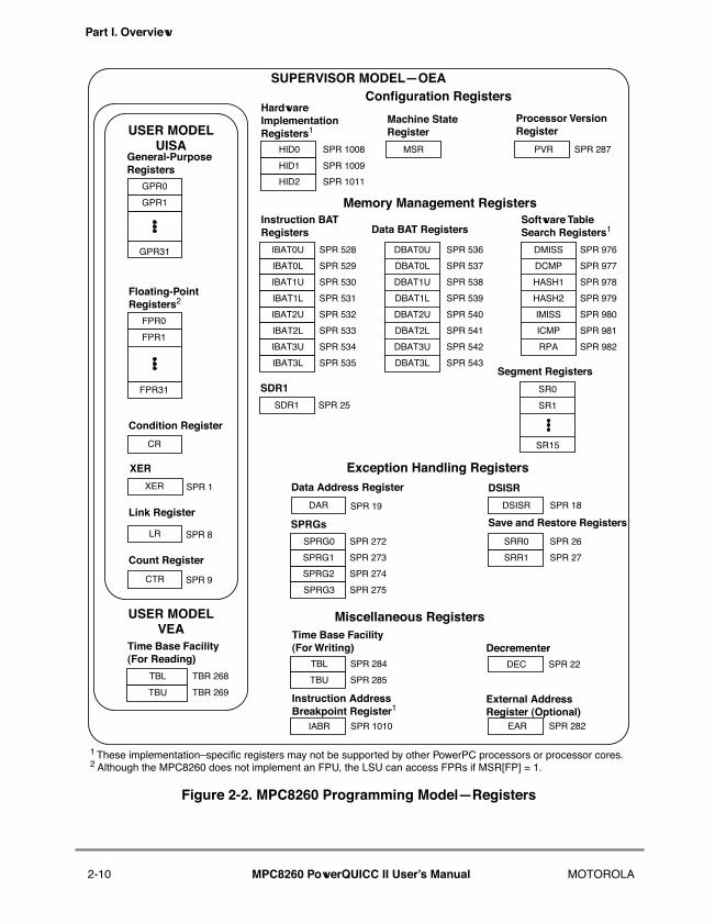
Part I. Overview
Figure 2-2. MPC8260 Programming ModelÑRegisters
DSISR
SPR 18DSISR
Data Address Register
SPR 19DAR
SPR 26SRR0
SPR 27SRR1
SPRGs
SPR 272SPRG0
SPR 273SPRG1
SPR 274SPRG2
SPR 275SPRG3
Exception Handling Registers
Save and Restore Registers
Instruction BATRegisters
SPR 528IBAT0U
SPR 529IBAT0L
SPR 530IBAT1U
SPR 531IBAT1L
SPR 532IBAT2U
SPR 533IBAT2L
SPR 534IBAT3U
SPR 535IBAT3L
Data BAT Registers
SPR 536DBAT0U
SPR 537DBAT0L
SPR 538DBAT1U
SPR 539DBAT1L
SPR 540DBAT2U
SPR 541DBAT2L
SPR 542DBAT3U
SPR 543DBAT3L
Memory Management RegistersSoftware Table Search Registers1
SPR 976DMISS
SPR 977DCMP
SPR 978HASH1
SPR 979HASH2
SPR 980IMISS
SPR 981ICMP
SPR 982RPA
Machine StateRegister
MSR
Processor Version Register
SPR 287PVR
Configuration RegistersHardware ImplementationRegisters1
SPR 1008HID0
TBR 268TBL
TBR 269TBU
SPR 1
USER MODELUISA
Condition Register
GPR0
GPR1
GPR31
General-PurposeRegisters
Floating-PointRegisters2
XER
XER
SPR 8
Link Register
LR
Time Base Facility (For Reading)
SUPERVISOR MODELÑOEA
SPR 22
Decrementer
DEC
Time Base Facility(For Writing)
SPR 284TBL
SPR 285TBU
SPR 282
External AddressRegister (Optional)
EAR
SDR1
SPR 25SDR1
SPR 9
Count Register
CTR
Miscellaneous Registers
SPR 1010IABR
Instruction Address Breakpoint Register1
Segment Registers
SR0
SR1
SR15
FPR0
FPR1
FPR31
1 These implementationÐspecific registers may not be supported by other PowerPC processors or processor cores.
SPR 1009HID1
CR
.
USER MODELVEA
SPR 1011HID2
2 Although the MPC8260 does not implement an FPU, the LSU can access FPRs if MSR[FP] = 1.
2-10 MPC8260 PowerQUICC II UserÕs Manual MOTOROLA
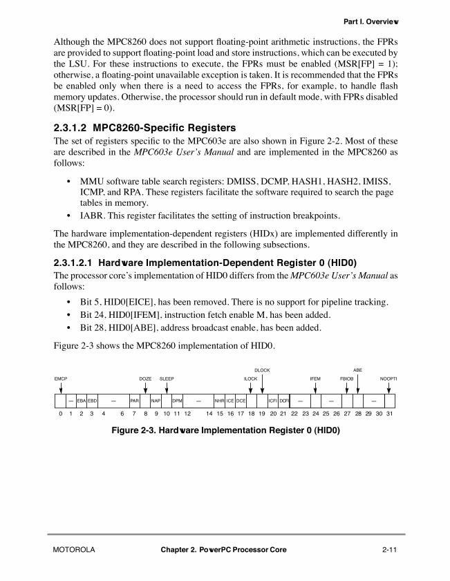
Part I. Overview
Although the MPC8260 does not support ßoating-point arithmetic instructions, the FPRsare provided to support ßoating-point load and store instructions, which can be executed bythe LSU. For these instructions to execute, the FPRs must be enabled (MSR[FP] = 1);otherwise, a ßoating-point unavailable exception is taken. It is recommended that the FPRsbe enabled only when there is a need to access the FPRs, for example, to handle ßashmemory updates. Otherwise, the processor should run in default mode, with FPRs disabled(MSR[FP] = 0).
2.3.1.2 MPC8260-SpeciÞc RegistersThe set of registers speciÞc to the MPC603e are also shown in Figure 2-2. Most of theseare described in the MPC603e UserÕs Manual and are implemented in the MPC8260 asfollows:
¥ MMU software table search registers: DMISS, DCMP, HASH1, HASH2, IMISS, ICMP, and RPA. These registers facilitate the software required to search the page tables in memory.
¥ IABR. This register facilitates the setting of instruction breakpoints.
The hardware implementation-dependent registers (HIDx) are implemented differently inthe MPC8260, and they are described in the following subsections.
2.3.1.2.1 Hardware Implementation-Dependent Register 0 (HID0)The processor coreÕs implementation of HID0 differs from the MPC603e UserÕs Manual asfollows:
¥ Bit 5, HID0[EICE], has been removed. There is no support for pipeline tracking.¥ Bit 24, HID0[IFEM], instruction fetch enable M, has been added. ¥ Bit 28, HID0[ABE], address broadcast enable, has been added.
Figure 2-3 shows the MPC8260 implementation of HID0.
Figure 2-3. Hardware Implementation Register 0 (HID0)
0 1 2 3 4 6 7 8 9 10 11 12 14 15 16 17 18 19 20 21 22 23 24 25 26 27 28 29 30 31
EBDEBA PAR NAP DPM NHR ICE DCE DCFI
EMCP DOZE SLEEP ILOCK
DLOCK
ICFI
FBIOB NOOPTI
Ñ Ñ Ñ
IFEM
Ñ Ñ Ñ
ABE
MOTOROLA Chapter 2. PowerPC Processor Core 2-11
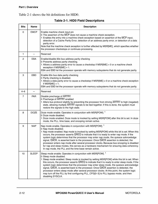
Part I. Overview
Table 2-1 shows the bit deÞnitions for HID0.
Table 2-1. HID0 Field Descriptions
Bits Name Description
0 EMCP Enable machine check input pin0 The assertion of the MCP does not cause a machine check exception. 1 Enables the entry into a machine check exception based on assertion of the MCP input,
detection of a Cache Parity Error, detection of an address parity error, or detection of a data parity error.
Note that the machine check exception is further affected by MSR[ME], which speciÞes whether the processor checkstops or continues processing.
1 Ñ Reserved
2 EBA Enable/disable 60x bus address parity checking 0 Prevents address parity checking.1 Allows a address parity error to cause a checkstop if MSR[ME] = 0 or a machine check
exception if MSR[ME] = 1.EBA and EBD let the processor operate with memory subsystems that do not generate parity.
3 EBD Enable 60x bus data parity checking0 Parity checking is disabled.1 Allows a data parity error to cause a checkstop if MSR[ME] = 0 or a machine check exception
if MSR[ME] = 1.EBA and EBD let the processor operate with memory subsystems that do not generate parity.
4Ð6 Ñ Reserved
7 PAR Disable precharge of ARTRY.0 Precharge of ARTRY enabled1 Alters bus protocol slightly by preventing the processor from driving ARTRY to high (negated)
state, allowing multiple ARTRY signals to be tied together. If this is done, the system must restore the signals to the high state.
8 DOZE Doze mode enable. Operates in conjunction with MSR[POW]. 1
0 Doze mode disabled.1 Doze mode enabled. Doze mode is invoked by setting MSR[POW] after this bit is set. In doze
mode, the PLL, time base, and snooping remain active.
9 NAP Nap mode enable. Operates in conjunction with MSR[POW]. 1
0 Nap mode disabled.1 Nap mode enabled. Nap mode is invoked by setting MSR[POW] while this bit is set. When this
occurs, the processor asserts QREQ to indicate that it is ready to enter nap mode. If the system logic determines that the processor may enter nap mode, the quiesce acknowledge signal, QACK, is asserted back to the processor. Once QACK assertion is detected, the processor enters nap mode after several processor clocks. Because bus snooping is disabled for nap and sleep modes, this serves as a hardware mechanism for ensuring data coherency. In nap mode, the PLL and the time base remain active.
10 SLEEP Sleep mode enable. Operates in conjunction with MSR[POW]. 1
0 Sleep mode disabled.1 Sleep mode enabled. Sleep mode is invoked by setting MSR[POW] while this bit is set. When
this occurs, the processor asserts QREQ to indicate that it is ready to enter sleep mode. If the system logic determines that the processor may enter sleep mode, the quiesce acknowledge signal, QACK, is asserted back to the processor. Once QACK assertion is detected, the processor enters sleep mode after several processor clocks. At this point, the system logic may turn off the PLL by Þrst conÞguring PLL_CFG[0Ð3] to PLL bypass mode, and then disabling SYSCLK.
2-12 MPC8260 PowerQUICC II UserÕs Manual MOTOROLA
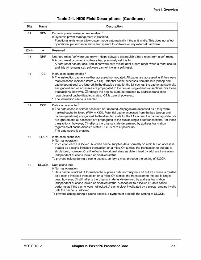
Part I. Overview
11 DPM Dynamic power management enable. 1
0 Dynamic power management is disabled.1 Functional units enter a low-power mode automatically if the unit is idle. This does not affect
operational performance and is transparent to software or any external hardware.
12Ð14 Ñ Reserved
15 NHR Not hard reset (software-use only)ÑHelps software distinguish a hard reset from a soft reset. 0 A hard reset occurred if software had previously set this bit.1 A hard reset has not occurred. If software sets this bit after a hard reset, when a reset occurs
and this bit remains set, software can tell it was a soft reset.
16 ICE Instruction cache enable 2
0 The instruction cache is neither accessed nor updated. All pages are accessed as if they were marked cache-inhibited (WIM = X1X). Potential cache accesses from the bus (snoop and cache operations) are ignored. In the disabled state for the L1 caches, the cache tag state bits are ignored and all accesses are propagated to the bus as single-beat transactions. For those transactions, however, CI reßects the original state determined by address translation regardless of cache disabled status. ICE is zero at power-up.
1 The instruction cache is enabled
17 DCE Data cache enable 2
0 The data cache is neither accessed nor updated. All pages are accessed as if they were marked cache-inhibited (WIM = X1X). Potential cache accesses from the bus (snoop and cache operations) are ignored. In the disabled state for the L1 caches, the cache tag state bits are ignored and all accesses are propagated to the bus as single-beat transactions. For those transactions, however, CI reßects the original state determined by address translation regardless of cache disabled status. DCE is zero at power-up.
1 The data cache is enabled.
18 ILOCK Instruction cache lock0 Normal operation 1 Instruction cache is locked. A locked cache supplies data normally on a hit, but an access is
treated as a cache-inhibited transaction on a miss. On a miss, the transaction to the bus is single-beat, however, CI still reßects the original state as determined by address translation independent of cache locked or disabled status.
To prevent locking during a cache access, an isync must precede the setting of ILOCK.
19 DLOCK Data cache lock 0 Normal operation1 Data cache is locked. A locked cache supplies data normally on a hit but an access is treated
as a cache-inhibited transaction on a miss. On a miss, the transaction to the bus is single-beat, however, CI still reßects the original state as determined by address translation independent of cache locked or disabled status. A snoop hit to a locked L1 data cache performs as if the cache were not locked. A cache block invalidated by a snoop remains invalid until the cache is unlocked.
To prevent locking during a cache access, a sync must precede the setting of DLOCK.
Table 2-1. HID0 Field Descriptions (Continued)
Bits Name Description
MOTOROLA Chapter 2. PowerPC Processor Core 2-13
Part I. Overview
2.3.1.2.2 Hardware Implementation-Dependent Register 1 (HID1)The MPC8260 implementation of HID1 is shown in Figure 2-4.
20 ICFI Instruction cache ßash invalidate 2
0 The instruction cache is not invalidated. The bit is cleared when the invalidation operation begins (usually the next cycle after the write operation to the register). The instruction cache must be enabled for the invalidation to occur.
1 An invalidate operation is issued that marks the state of each instruction cache block as invalid without writing back modiÞed cache blocks to memory. Cache access is blocked during this time. Bus accesses to the cache are signaled as a miss during invalidate-all operations. Setting ICFI clears all the valid bits of the blocks and the PLRU bits to point to way L0 of each set. Once the L1 ßash invalidate bits are set through an mtspr instruction, hardware automatically resets these bits in the next cycle (provided that the corresponding cache enable bits are set in HID0).
21 DCFI Data cache ßash invalidate 2
0 The data cache is not invalidated. The bit is cleared when the invalidation operation begins (usually the next cycle after the write operation to the register). The data cache must be enabled for the invalidation to occur.
1 An invalidate operation is issued that marks the state of each data cache block as invalid without writing back modiÞed cache blocks to memory. Cache access is blocked during this time. Bus accesses to the cache are signaled as a miss during invalidate-all operations. Setting DCFI clears all the valid bits of the blocks and the PLRU bits to point to way L0 of each set. Once the L1 ßash invalidate bits are set through an mtspr instruction, hardware automatically resets these bits in the next cycle (provided that the corresponding cache enable bits are set in HID0).
22Ð23 Ñ Reserved
24 IFEM Enable M bit on 60x bus for instruction fetches0 M bit not reßected on 60x bus. Instruction fetches are treated as nonglobal on the bus.1 Instruction fetches reßect the M bit from the WIM settings on the 60x bus.
25Ð26 Ñ Reserved
27 FBIOB Force branch indirect on bus. 0 Register indirect branch targets are fetched normally1 Forces register indirect branch targets to be fetched externally.
28 ABE Address broadcast enable 0 dcbf, dcbi, and dcbst instructions are not broadcast on the 60x bus. 1 dcbf, dcbi, and dcbst generate address-only broadcast operations on the 60x bus.
29Ð30 Ñ Reserved
31 NOOPTI No-op the data cache touch instructions.0 The dcbt and dcbtst instructions are enabled. 1 The dcbt and dcbtst instructions are no-oped globally.
1 See Chapter 9, ÒPower Management,Ó of the MPC603e UserÕs Manual for more information.2 See Chapter 3, ÒInstruction and Data Cache Operation,Ó of the MPC603e UserÕs Manual for more information.
Table 2-1. HID0 Field Descriptions (Continued)
Bits Name Description
2-14 MPC8260 PowerQUICC II UserÕs Manual MOTOROLA
Part I. Overview
Figure 2-4. Hardware Implementation Register 1 (HID1)
Table 2-2 shows the bit deÞnitions for HID1.
2.3.1.2.3 Hardware Implementation-Dependent Register 2 (HID2)The processor core implements an additional hardware implementation-dependent registernot described in the MPC603e UserÕs Manual, shown in Figure 2-5.
Figure 2-5. Hardware Implementation-Dependent Register 2 (HID2)
Table 2-3 describes the HID2 Þelds.
Table 2-2. HID1 Field Descriptions
Bits Name Function
0Ð4 PLLCFG PLL conÞguration setting
5Ð31 Ñ Reserved
Table 2-3. HID2 Field Descriptions
Bits Name Function
0Ð14 Ñ Reserved
15 SFP Speed for low power. Setting SFP reduces power consumption at the cost of reducing the maximum frequency, which beneÞts power-sensitive applications that are not frequency-critical.
16Ð18 IWLCK Instruction cache way lock. Useful for locking blocks of instructions into the instruction cache for time-critical applications that require deterministic behavior. See Section 2.4.2.3, ÒCache Locking.Ó
19Ð23 Ñ Reserved
24Ð26 DWLCK Data cache way lock. Useful for locking blocks of data into the data cache for time-critical applications where deterministic behavior is required. See Section 2.4.2.3, ÒCache Locking.Ó
27Ð31 Ñ Reserved
0 4 5 31
ÑPLLCFG
0 14 15 16 18 19 23 24 26 27 31
SFP IWLCK DWLCKÑ Ñ Ñ
MOTOROLA Chapter 2. PowerPC Processor Core 2-15
Part I. Overview
2.3.1.2.4 Processor Version Register (PVR)Software can identify the MPC8260Õs processor core by reading the processor versionregister (PVR). The MPC8260Õs processor version number is 0x0081; the processorrevision level starts at 0x0100 and is incremented for each revision of the chip.
2.3.2 PowerPC Instruction Set and Addressing ModesAll PowerPC instructions are encoded as single-word (32-bit) opcodes. Instruction formatsare consistent among all instruction types, permitting efÞcient decoding to occur in parallelwith operand accesses. This Þxed instruction length and consistent format greatly simpliÞesinstruction pipelining.
2.3.2.1 Calculating Effective Addresses The effective address (EA) is the 32-bit address computed by the processor when executinga memory access or branch instruction or when fetching the next sequential instruction.
The PowerPC architecture supports two simple memory addressing modes:
¥ EA = (rA|0) + offset (including offset = 0) (register indirect with immediate index)
¥ EA = (rA|0) + rB (register indirect with index)
These simple addressing modes allow efÞcient address generation for memory accesses.Calculation of the effective address for aligned transfers occurs in a single clock cycle.
For a memory access instruction, if the sum of the effective address and the operand lengthexceeds the maximum effective address, the memory operand is considered to wrap aroundfrom the maximum effective address to effective address 0.
Effective address computations for both data and instruction accesses use 32-bit unsignedbinary arithmetic. A carry from bit 0 is ignored in 32-bit implementations.
In addition to the functionality of the MPC603e, the MPC8260 has additional hardwaresupport for misaligned little-endian accesses. Except for string/multiple load and storeinstructions, little-endian load/store accesses not on a word boundary generate exceptionsunder the same circumstances as big-endian requests.
2.3.2.2 PowerPC Instruction SetThe PowerPC instructions are divided into the following categories:
¥ Integer instructionsÑThese include arithmetic and logical instructions.
Ñ Integer arithmetic Ñ Integer compare Ñ Integer logical Ñ Integer rotate and shift
2-16 MPC8260 PowerQUICC II UserÕs Manual MOTOROLA
Part I. Overview
¥ Load/store instructionsÑThese include integer and ßoating-point load and store instructions.
Ñ Integer load and storeÑ Integer load and store with byte reverseÑ Integer load and store string/multiple Ñ Floating-point load and store. Setting MSR[FPE] allows the MPC8260 to access
the FPRs with the ßoating-point load and store instructions described in the MPC603e UserÕs Manual. This is useful both for systems that require emulation of ßoating-point instructions and for increasing data throughput.
¥ Flow control instructionsÑThese include branching instructions, condition register logical instructions, trap instructions, and other synchronizing instructions that affect the instruction ßow.
Ñ Branch and trap Ñ Condition register logical Ñ Primitives used to construct atomic memory operations (lwarx and stwcx.)Ñ Synchronize
¥ Processor control instructionsÑThese instructions are used for synchronizing memory accesses and management of caches, TLBs, and the segment registers.
Ñ Move to/from SPR Ñ Move to/from MSRÑ Instruction synchronize
¥ Memory control instructionsÑThese provide control of caches, TLBs, and segment registers.
Ñ Supervisor-level cache management Ñ User-level cache managementÑ Segment register manipulation Ñ TLB management
Note that this grouping of the instructions does not indicate which execution unit executesa particular instruction or group of instructions.
Integer instructions operate on byte, half-word, and word operands. The PowerPCarchitecture uses instructions that are four bytes long and word-aligned. It provides forbyte, half-word, and word operand loads and stores between memory and a set of 32 GPRs.It also provides for word and double-word operand loads and stores between memory anda set of 32 ßoating-point registers (FPRs). Although the MPC8260 does use the FPRs for64-bit loads and stores, it does not support ßoating-point arithmetic instructions.
2-17 MPC8260 PowerQUICC II UserÕs Manual MOTOROLA
Part I. Overview
Computational instructions do not modify memory. To use a memory operand in acomputation and then modify the same or another memory location, the memory contentsmust be loaded into a register, modiÞed, and then written back to the target location withseparate instructions. Decoupling arithmetic instructions from memory accesses increasesthroughput by facilitating pipelining.
PowerPC processors follow the program ßow when they are in the normal execution state.However, the ßow of instructions can be interrupted directly by the execution of aninstruction or by an asynchronous event. Either kind of exception may cause one of severalcomponents of the system software to be invoked.
2.3.2.3 MPC8260 Implementation-SpeciÞc Instruction SetThe MPC8260 processor core instruction set is deÞned as follows:
¥ The processor core provides hardware support for all 32-bit PowerPC instructions.
¥ The processor core provides two implementation-speciÞc instructions used for software table search operations following TLB misses:
Ñ Load Data TLB Entry (tlbld)
Ñ Load Instruction TLB Entry (tlbli)
¥ The processor core implements the following instructions deÞned as optional by the PowerPC architecture:
Ñ External Control In Word Indexed (eciwx)
Ñ External Control Out Word Indexed (ecowx)
Ñ Store Floating-Point as Integer Word Indexed (stÞwx)
The MPC8260 does not provide the hardware support for misaligned eciwx and ecowx instructions provided by the MPC603e processor. An alignment exception is taken if these instructions are not word-aligned.
2.4 Cache ImplementationThe MPC8260 processor core has separate data and instruction caches. The cacheimplementation is described in the following sections.
2.4.1 PowerPC Cache ModelThe PowerPC architecture does not deÞne hardware aspects of cache implementations. Forexample, some PowerPC processors, including the MPC8260Õs processor core, haveseparate instruction and data caches (Harvard architecture), while others, such as thePowerPC 601¨ microprocessor, implement a uniÞed cache.
2-18 MPC8260 PowerQUICC II UserÕs Manual MOTOROLA
Part I. Overview
PowerPC microprocessors control the following memory access modes on a page or blockbasis:
¥ Write-back/write-through mode
¥ Caching-inhibited mode
¥ Memory coherency
The PowerPC cache management instructions provide a means by which the applicationprogrammer can affect the cache contents.
2.4.2 MPC8260 Implementation-SpeciÞc Cache ImplementationAs shown in Figure 2-1, the caches provide a 64-bit interface to the instruction fetch unitand load/store unit. The surrounding logic selects, organizes, and forwards the requestedinformation to the requesting unit. Write operations to the cache can be performed on a bytebasis, and a complete read-modify-write operation to the cache can occur in each cycle.
Each cache block contains eight contiguous words from memory that are loaded from an8-word boundary (that is, bits A27ÐA31 of the effective addresses are zero); thus, a cacheblock never crosses a page boundary. Misaligned accesses across a page boundary can incura performance penalty.
The cache blocks are loaded in to the processor core in four beats of 64 bits each. The burstload is performed as critical double word Þrst.
To ensure coherency among caches in a multiprocessor (or multiple caching-device)implementation, the processor core implements the MEI protocol. These three states,modiÞed, exclusive, and invalid, indicate the state of the cache block as follows:
¥ ModiÞedÑThe cache block is modiÞed with respect to system memory; that is, data for this address is valid only in the cache and not in system memory.
¥ ExclusiveÑThis cache block holds valid data that is identical to the data at this address in system memory. No other cache has this data.
¥ InvalidÑThis cache block does not hold valid data.
2.4.2.1 Data CacheAs shown in Figure 2-6, the data cache is conÞgured as 128 sets of four blocks each. Eachblock consists of 32 bytes, two state bits, and an address tag. The two state bits implementthe three-state MEI (modiÞed/exclusive/invalid) protocol. Each block contains eight 32-bitwords. Note that the PowerPC architecture deÞnes the term ÔblockÕ as the cacheable unit.For the MPC8260Õs processor core, the block size is equivalent to a cache line.
MOTOROLA Chapter 2. PowerPC Processor Core 2-19
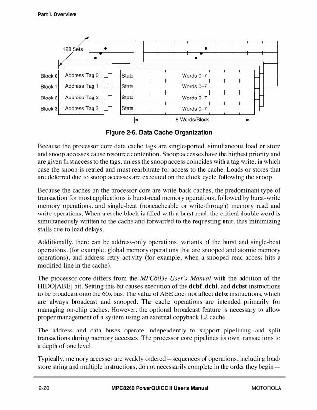
Part I. Overview
Figure 2-6. Data Cache Organization
Because the processor core data cache tags are single-ported, simultaneous load or storeand snoop accesses cause resource contention. Snoop accesses have the highest priority andare given Þrst access to the tags, unless the snoop access coincides with a tag write, in whichcase the snoop is retried and must rearbitrate for access to the cache. Loads or stores thatare deferred due to snoop accesses are executed on the clock cycle following the snoop.
Because the caches on the processor core are write-back caches, the predominant type oftransaction for most applications is burst-read memory operations, followed by burst-writememory operations, and single-beat (noncacheable or write-through) memory read andwrite operations. When a cache block is Þlled with a burst read, the critical double word issimultaneously written to the cache and forwarded to the requesting unit, thus minimizingstalls due to load delays.
Additionally, there can be address-only operations, variants of the burst and single-beatoperations, (for example, global memory operations that are snooped and atomic memoryoperations), and address retry activity (for example, when a snooped read access hits amodiÞed line in the cache).
The processor core differs from the MPC603e UserÕs Manual with the addition of theHIDO[ABE] bit. Setting this bit causes execution of the dcbf, dcbi, and dcbst instructionsto be broadcast onto the 60x bus. The value of ABE does not affect dcbz instructions, whichare always broadcast and snooped. The cache operations are intended primarily formanaging on-chip caches. However, the optional broadcast feature is necessary to allowproper management of a system using an external copyback L2 cache.
The address and data buses operate independently to support pipelining and splittransactions during memory accesses. The processor core pipelines its own transactions toa depth of one level.
Typically, memory accesses are weakly orderedÑsequences of operations, including load/store string and multiple instructions, do not necessarily complete in the order they beginÑ
Address Tag 1
Address Tag 2
Address Tag 3
Block 1
Block 2
Block 3
128 Sets
Address Tag 0Block 0
8 Words/Block
State
State
State
Words 0Ð7
Words 0Ð7
Words 0Ð7
Words 0Ð7State
2-20 MPC8260 PowerQUICC II UserÕs Manual MOTOROLA
Part I. Overview
maximizing the efÞciency of the internal bus without sacriÞcing coherency of the data. Theprocessor core allows pending read operations to precede previous store operations (exceptwhen a dependency exists, or in cases where a non-cacheable access is performed), andprovides support for a write operation to proceed a previously queued read data tenure (forexample, allowing a snoop push to be enveloped by the address and data tenures of a readoperation). Because the processor can dynamically optimize run-time ordering of load/store trafÞc, overall performance is improved.
2.4.2.2 Instruction CacheThe instruction cache also consists of 128 sets of four blocks, and each block consists of 32bytes, an address tag, and a valid bit. The instruction cache may not be written to exceptthrough a block Þll operation caused by a cache miss. In the processor core, internal accessto the instruction cache is blocked only until the critical load completes.
The processor core supports instruction fetching from other instruction cache linesfollowing the forwarding of the critical Þrst double word of a cache line load operation. Theprocessor coreÕs instruction cache is blocked only until the critical load completes (hitsunder reloads allowed). Successive instruction fetches from the cache line being loaded areforwarded, and accesses to other instruction cache lines can proceed during the cache lineload operation.
The instruction cache is not snooped, and cache coherency must be maintained by software.A fast hardware invalidation capability is provided to support cache maintenance. Theorganization of the instruction cache is very similar to the data cache shown in Figure 2-6.
2.4.2.3 Cache LockingThe processor core supports cache locking, which is the ability to prevent some or all of amicroprocessorÕs instruction or data cache from being overwritten. Cache entries can belocked for either an entire cache or for individual ways within the cache. Entire data cachelocking is enabled by setting HID0[DLOCK], and entire instruction cache locking isenabled by setting HID0[ILOCK]. For more information, refer to Cache Locking on the G2Core application note (order number: AN1767/D). Cache way locking is controlled by theIWLCK and DWLCK bits of HID2.
2.4.2.3.1 Entire Cache LockingWhen an entire cache is locked, hits within the cache are supplied in the same manner ashits to an unlocked cache. Any access that misses in the cache is treated as a cache-inhibitedaccess. Cache entries that are invalid at the time of locking will remain invalid andinaccessible until the cache is unlocked. Once the cache has been unlocked, all entries(including invalid entries) are available. Entire cache locking is inefÞcient if the number ofinstructions or the size of data to be locked is small compared to the cache size.
2.4.2.3.2 Way LockingLocking only a portion of the cache is accomplished by locking ways within the cache.Locking always begins with the Þrst way (way0) and is sequential. That is, it is valid to lock
MOTOROLA Chapter 2. PowerPC Processor Core 2-21
Part I. Overview
ways 0, 1, and 2 but it is not possible to lock just way0 and way2). When using way lockingat least one way must be left unlocked. The maximum number of lockable ways is three.
Unlike entire cache locking, invalid entries in a locked way are accessible and available fordata placement. As hits to the cache Þll invalid entries within a locked way, the entriesbecome valid and locked. This behavior differs from entire cache locking where nothing isplaced in the cache, even if invalid entries exist in the cache. Unlocked ways of the cachebehave normally.
2.5 Exception ModelThis section describes the PowerPC exception model and implementation-speciÞc detailsof the MPC8260 core.
2.5.1 PowerPC Exception ModelThe PowerPC exception mechanism allows the processor to change to supervisor state as aresult of external signals, errors, or unusual conditions arising in the execution ofinstructions. When exceptions occur, information about the state of the processor is savedto certain registers and the processor begins execution at an address (exception vector)predetermined for each exception. Processing of exceptions occurs in supervisor mode.
Although multiple exception conditions can map to a single exception vector, a morespeciÞc condition may be determined by examining a register associated with theexceptionÑfor example, the DSISR identiÞes instructions that cause a DSI exception.Additionally, some exception conditions can be explicitly enabled or disabled by software.
The PowerPC architecture requires that exceptions be handled in program order; therefore,although a particular implementation may recognize exception conditions out of order,exceptions are taken in strict order. When an instruction-caused exception is recognized,any unexecuted instructions that appear earlier in the instruction stream, including any thathave not yet entered the execute stage, are required to complete before the exception istaken. Any exceptions caused by those instructions are handled Þrst. Likewise, exceptionsthat are asynchronous and precise are recognized when they occur, but are not handled untilthe instruction currently in the completion stage successfully completes execution orgenerates an exception, and the completed store queue is emptied.
Unless a catastrophic condition causes a system reset or machine check exception, only oneexception is handled at a time. If, for example, a single instruction encounters multipleexception conditions, those conditions are handled sequentially. After the exception handlerhandles an exception, the instruction execution continues until the next exception conditionis encountered. However, in many cases there is no attempt to re-execute the instruction.This method of recognizing and handling exception conditions sequentially guarantees thatexceptions are recoverable.
Exception handlers should save the information stored in SRR0 and SRR1 early to preventthe program state from being lost due to a system reset or machine check exception or to
2-22 MPC8260 PowerQUICC II UserÕs Manual MOTOROLA
Part I. Overview
an instruction-caused exception in the exception handler. SRR0 and SRR1 should also besaved before enabling external interrupts.
The PowerPC architecture supports four types of exceptions:
¥ Synchronous, preciseÑThese are caused by instructions. All instruction-caused exceptions are handled precisely; that is, the machine state at the time the exception occurs is known and can be completely restored. This means that (excluding the trap and system call exceptions) the address of the faulting instruction is provided to the exception handler and that neither the faulting instruction nor subsequent instructions in the code stream will complete execution before the exception is taken. Once the exception is processed, execution resumes at the address of the faulting instruction (or at an alternate address provided by the exception handler). When an exception is taken due to a trap or system call instruction, execution resumes at an address provided by the handler.
¥ Synchronous, impreciseÑThe PowerPC architecture deÞnes two imprecise ßoating-point exception modes, recoverable and nonrecoverable. These are not implemented on the MPC8260.
¥ Asynchronous, maskableÑThe external, system management interrupt (SMI), and decrementer interrupts are maskable asynchronous exceptions. When these exceptions occur, their handling is postponed until the next instruction and any exceptions associated with that instruction complete execution. If no instructions are in the execution units, the exception is taken immediately upon determination of the correct restart address (for loading SRR0).
¥ Asynchronous, nonmaskableÑThere are two nonmaskable asynchronous exceptions: system reset and the machine check exception. These exceptions may not be recoverable, or may provide a limited degree of recoverability. All exceptions report recoverability through MSR[RI].
2.5.2 MPC8260 Implementation-SpeciÞc Exception ModelAs speciÞed by the PowerPC architecture, all processor core exceptions can be describedas either precise or imprecise and either synchronous or asynchronous. Asynchronousexceptions (some of which are maskable) are caused by events external to the processorÕsexecution. Synchronous exceptions, which are all handled precisely by the processor core,are caused by instructions. The processor core exception classes are shown in Table 2-4.
MOTOROLA Chapter 2. PowerPC Processor Core 2-23
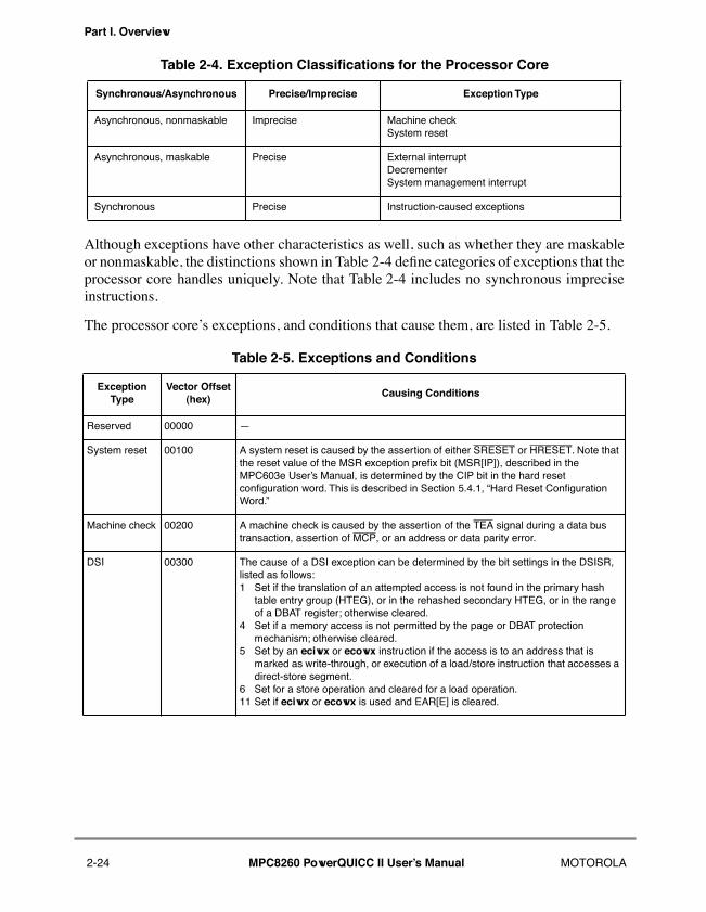
Part I. Overview
Although exceptions have other characteristics as well, such as whether they are maskableor nonmaskable, the distinctions shown in Table 2-4 deÞne categories of exceptions that theprocessor core handles uniquely. Note that Table 2-4 includes no synchronous impreciseinstructions.
The processor coreÕs exceptions, and conditions that cause them, are listed in Table 2-5.
Table 2-4. Exception Classifications for the Processor Core
Synchronous/Asynchronous Precise/Imprecise Exception Type
Asynchronous, nonmaskable Imprecise Machine checkSystem reset
Asynchronous, maskable Precise External interruptDecrementerSystem management interrupt
Synchronous Precise Instruction-caused exceptions
Table 2-5. Exceptions and Conditions
Exception Type
Vector Offset(hex)
Causing Conditions
Reserved 00000 Ñ
System reset 00100 A system reset is caused by the assertion of either SRESET or HRESET. Note that the reset value of the MSR exception preÞx bit (MSR[IP]), described in the MPC603e UserÕs Manual, is determined by the CIP bit in the hard reset conÞguration word. This is described in Section 5.4.1, ÒHard Reset ConÞguration Word.Ó
Machine check 00200 A machine check is caused by the assertion of the TEA signal during a data bus transaction, assertion of MCP, or an address or data parity error.
DSI 00300 The cause of a DSI exception can be determined by the bit settings in the DSISR, listed as follows:1 Set if the translation of an attempted access is not found in the primary hash
table entry group (HTEG), or in the rehashed secondary HTEG, or in the range of a DBAT register; otherwise cleared.
4 Set if a memory access is not permitted by the page or DBAT protection mechanism; otherwise cleared.
5 Set by an eciwx or ecowx instruction if the access is to an address that is marked as write-through, or execution of a load/store instruction that accesses a direct-store segment.
6 Set for a store operation and cleared for a load operation. 11 Set if eciwx or ecowx is used and EAR[E] is cleared.
2-24 MPC8260 PowerQUICC II UserÕs Manual MOTOROLA
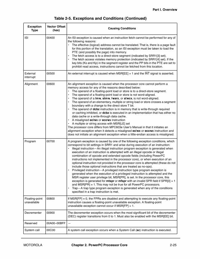
Part I. Overview
ISI 00400 An ISI exception is caused when an instruction fetch cannot be performed for any of the following reasons:¥ The effective (logical) address cannot be translated. That is, there is a page fault
for this portion of the translation, so an ISI exception must be taken to load the PTE (and possibly the page) into memory.
¥ The fetch access is to a direct-store segment (indicated by SRR1[3] set).¥ The fetch access violates memory protection (indicated by SRR1[4] set). If the
key bits (Ks and Kp) in the segment register and the PP bits in the PTE are set to prohibit read access, instructions cannot be fetched from this location.
External interrupt
00500 An external interrupt is caused when MSR[EE] = 1 and the INT signal is asserted.
Alignment 00600 An alignment exception is caused when the processor core cannot perform a memory access for any of the reasons described below:¥ The operand of a ßoating-point load or store is to a direct-store segment.¥ The operand of a ßoating-point load or store is not word-aligned.¥ The operand of a lmw, stmw, lwarx, or stwcx. is not word-aligned.¥ The operand of an elementary, multiple or string load or store crosses a segment
boundary with a change to the direct store T bit.¥ The operand of dcbz instruction is in memory that is write-through required or caching inhibited, or dcbz is executed in an implementation that has either no
data cache or a write-through data cache.¥ A misaligned eciwx or ecowx instruction¥ A multiple or string access with MSR[LE] setThe processor core differs from MPC603e UserÕs Manual in that it initiates an alignment exception when it detects a misaligned eciwx or ecowx instruction and does not initiate an alignment exception when a little-endian access is misaligned.
Program 00700 A program exception is caused by one of the following exception conditions, which correspond to bit settings in SRR1 and arise during execution of an instruction:¥ Illegal instructionÑAn illegal instruction program exception is generated when
execution of an instruction is attempted with an illegal opcode or illegal combination of opcode and extended opcode Þelds (including PowerPC instructions not implemented in the processor core), or when execution of an optional instruction not provided in the processor core is attempted (these do not include those optional instructions that are treated as no-ops).
¥ Privileged instructionÑA privileged instruction type program exception is generated when the execution of a privileged instruction is attempted and the MSR register user privilege bit, MSR[PR], is set. In the processor core, this exception is generated for mtspr or mfspr with an invalid SPR Þeld if SPR[0] = 1 and MSR[PR] = 1. This may not be true for all PowerPC processors.
¥ TrapÑA trap type program exception is generated when any of the conditions speciÞed in a trap instruction is met.
Floating-point unavailable
00800 If MSR[FP] = 0, the FPRs are disabled and attempting to execute any ßoating-point instruction causes a ßoating-point unavailable exception. A ßoating-point unavailable exception cannot occur if MSR[FP] = 1.
Decrementer 00900 The decrementer exception occurs when the most signiÞcant bit of the decrementer (DEC) register transitions from 0 to 1. Must also be enabled with the MSR[EE] bit.
Reserved 00A00Ð00BFF Ñ
System call 00C00 A system call exception occurs when a System Call (sc) instruction is executed.
Table 2-5. Exceptions and Conditions (Continued)
Exception Type
Vector Offset(hex)
Causing Conditions
MOTOROLA Chapter 2. PowerPC Processor Core 2-25
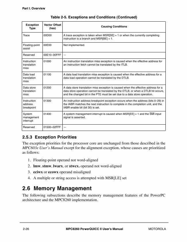
Part I. Overview
2.5.3 Exception PrioritiesThe exception priorities for the processor core are unchanged from those described in theMPC603e UserÕs Manual except for the alignment exception, whose causes are prioritizedas follows:
1. Floating-point operand not word-aligned
2. lmw, stmw, lwarx, or stwcx. operand not word-aligned
3. eciwx or ecowx operand misaligned
4. A multiple or string access is attempted with MSR[LE] set
2.6 Memory ManagementThe following subsections describe the memory management features of the PowerPCarchitecture and the MPC8260 implementation.
Trace 00D00 A trace exception is taken when MSR[SE] = 1 or when the currently completing instruction is a branch and MSR[BE] = 1.
Floating-point assist
00E00 Not implemented.
Reserved 00E10Ð00FFF Ñ
Instruction translation miss
01000 An instruction translation miss exception is caused when the effective address for an instruction fetch cannot be translated by the ITLB.
Data load translation miss
01100 A data load translation miss exception is caused when the effective address for a data load operation cannot be translated by the DTLB.
Data store translation miss
01200 A data store translation miss exception is caused when the effective address for a data store operation cannot be translated by the DTLB, or when a DTLB hit occurs, and the changed bit in the PTE must be set due to a data store operation.
Instruction address breakpoint
01300 An instruction address breakpoint exception occurs when the address (bits 0Ð29) in the IABR matches the next instruction to complete in the completion unit, and the IABR enable bit (bit 30) is set.
System management interrupt
01400 A system management interrupt is caused when MSR[EE] = 1 and the SMI input signal is asserted.
Reserved 01500Ð02FFF Ñ
Table 2-5. Exceptions and Conditions (Continued)
Exception Type
Vector Offset(hex)
Causing Conditions
2-26 MPC8260 PowerQUICC II UserÕs Manual MOTOROLA
Part I. Overview
2.6.1 PowerPC MMU ModelThe primary functions of the MMU are to translate logical (effective) addresses to physicaladdresses for memory accesses, and to provide access protection on blocks and pages ofmemory.
There are two types of accesses generated by the processor core that require addresstranslationÑinstruction accesses and data accesses to memory generated by load and storeinstructions.
The PowerPC MMU and exception models support demand-paged virtual memory. Virtualmemory management permits execution of programs larger than the size of physicalmemory; demand-paged implies that individual pages are loaded into physical memoryfrom system memory only when they are Þrst accessed by an executing program.
The PowerPC architecture supports the following three translation methods:
¥ Address translations disabled. Translation is enabled by setting bits in the MSRÑMSR[IR] enables instruction address translations and MSR[DR] enables data address translations. Clearing these bits disables translation and the effective address is used as the physical address.
¥ Block address translation. The PowerPC architecture deÞnes independent four-entry BAT arrays for instructions and data that maintain address translations for blocks of memory. Block sizes range from 128 Kbyte to 256 Mbyte and are software selectable. The BAT arrays are maintained by system software. The BAT registers, deÞned by the PowerPC architecture for block address translations, are shown in Figure 2-2.
¥ Demand page mode. The page table contains a number of page table entry groups (PTEGs). A PTEG contains eight page table entries (PTEs) of eight bytes each; therefore, each PTEG is 64 bytes long. PTEG addresses are entry points for table search operations.
The hashed page table is a variable-sized data structure that deÞnes the mapping between virtual page numbers and physical page numbers. The page table size is a power of 2, and its starting address is a multiple of its size.
On-chip instruction and data TLBs provide address translation in parallel with the on-chip cache access, incurring no additional time penalty in the event of a TLB hit. A TLB is a cache of the most recently used page table entries. Software is responsible for maintaining the consistency of the TLB with memory. In the MPC8260, the processor coreÕs TLBs are 64-entry, two-way set-associative caches that contain instruction and data address translations. The MPC8260Õs core provides hardware assist for software table search operations through the hashed page table on TLB misses. Supervisor software can invalidate TLB entries selectively.
The MMU also directs the address translation and enforces the protection hierarchyprogrammed by the operating system in relation to the supervisor/user privilege level of theaccess and in relation to whether the access is a load or store.
MOTOROLA Chapter 2. PowerPC Processor Core 2-27
Part I. Overview
2.6.2 MPC8260 Implementation-SpeciÞc MMU FeaturesThe instruction and data MMUs in the processor core provide 4-Gbytes of logical addressspace accessible to supervisor and user programs with a 4-Kbyte page size and 256-Mbytesegment size.
The MPC8260Õs MMUs support up to 4 Petabytes (252) of virtual memory and 4 Gbytes(232) of physical memory (referred to as real memory in the PowerPC architecturespeciÞcation) for instructions and data. Referenced and changed status is maintained by theprocessor for each page to assist implementation of a demand-paged virtual memorysystem.
The MPC8260Õs TLBs are 64-entry, two-way set-associative caches that contain instructionand data address translations. The processor core provides hardware assist for softwaretable search operations through the hashed page table on TLB misses. Supervisor softwarecan invalidate TLB entries selectively.
After an effective address is generated, the higher-order bits of the effective address aretranslated by the appropriate MMU into physical address bits. Simultaneously, the lower-order address bits (that are untranslated and therefore, considered both logical andphysical), are directed to the on-chip caches where they form the index into the four-wayset-associative tag array. After translating the address, the MMU passes the higher-orderbits of the physical address to the cache, and the cache lookup completes. For caching-inhibited accesses or accesses that miss in the cache, the untranslated lower-order addressbits are concatenated with the translated higher-order address bits; the resulting 32-bitphysical address is then used by the system interface, which accesses external memory.
For instruction accesses, the MMU performs an address lookup in both the 64 entries of theITLB, and in the IBAT array. If an effective address hits in both the ITLB and the IBATarray, the IBAT array translation takes priority. Data accesses cause a lookup in the DTLBand DBAT array for the physical address translation. In most cases, the physical addresstranslation resides in one of the TLBs and the physical address bits are readily available tothe on-chip cache.
When the physical address translation misses in the TLBs, the processor core provideshardware assistance for software to search the translation tables in memory. When arequired TLB entry is not found in the appropriate TLB, the processor vectors to one of thethree TLB miss exception handlers so that the softawre can perform a table search operationand load the TLB. When this occurs, the processor automatically saves information aboutthe access and the executing context. Refer to the MPC603e UserÕs Manual for moredetailed information about these features and the suggested software routines for searchingthe page tables.
2-28 MPC8260 PowerQUICC II UserÕs Manual MOTOROLA
Part I. Overview
2.7 Instruction TimingThe processor core is a pipelined superscalar processor. A pipelined processor is one inwhich the processing of an instruction is broken into discrete stages. Because theprocessing of an instruction is broken into a series of stages, an instruction does not requirethe entire resources of an execution unit at one time. For example, after an instructioncompletes the decode stage, it can pass on to the next stage, while the subsequentinstruction can advance into the decode stage. This improves the throughput of theinstruction ßow. The instruction pipeline in the processor core has four major stages,described as follows:
¥ The fetch pipeline stage primarily involves retrieving instructions from the memory system and determining the location of the next instruction fetch. Additionally, the BPU decodes branches during the fetch stage and folds out branch instructions before the dispatch stage if possible.
¥ The dispatch pipeline stage is responsible for decoding the instructions supplied by the instruction fetch stage, and determining which of the instructions are eligible to be dispatched in the current cycle. In addition, the source operands of the instructions are read from the appropriate register Þle and dispatched with the instruction to the execute pipeline stage. At the end of the dispatch pipeline stage, the dispatched instructions and their operands are latched by the appropriate execution unit.
¥ During the execute pipeline stage, each execution unit that has an executable instruction executes the selected instruction (perhaps over multiple cycles), writes the instruction's result into the appropriate rename register, and notiÞes the completion stage that the instruction has Þnished execution.
The execution unit reports any internal exceptions to the completion/writeback pipeline stage and discontinues execution until the exception is handled. The exception is not signaled until that instruction is the next to be completed. Execution of most load/store instructions is also pipelined. The load/store unit has two pipeline stages. The Þrst stage is for effective address calculation and MMU translation and the second stage is for accessing the data in the cache.
¥ The complete/writeback pipeline stage maintains the correct architectural machine state and transfers the contents of the rename registers to the GPRs and FPRs as instructions are retired. If the completion logic detects an instruction causing an exception, all following instructions are cancelled, their execution results in rename registers are discarded, and instructions are fetched from the correct instruction stream.
The processor core provides support for single-cycle store operations and it provides anadder/comparator in the SRU that allows the dispatch and execution of multiple integer addand compare instructions on each cycle.
Performance of integer divide operations has been improved in the processor core. A divideinstruction takes half the cycles to execute as described in the MPC603e UserÕs Manual.
MOTOROLA Chapter 2. PowerPC Processor Core 2-29
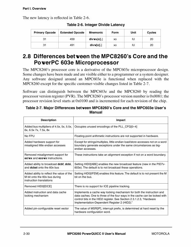
Part I. Overview
The new latency is reßected in Table 2-6.
2.8 Differences between the MPC8260Õs Core and the PowerPC 603e Microprocessor
The MPC8260Õs processor core is a derivative of the MPC603e microprocessor design.Some changes have been made and are visible either to a programmer or a system designer.Any software designed around an MPC603e is functional when replaced with theMPC8260 except for the speciÞc customer-visible changes listed in Table 2-7.
Software can distinguish between the MPC603e and the MPC8260 by reading theprocessor version register (PVR). The MPC8260Õs processor version number is 0x0081; theprocessor revision level starts at 0x0100 and is incremented for each revision of the chip.
Table 2-6. Integer Divide Latency
Primary Opcode Extended Opcode Mnemonic Form Unit Cycles
31 459 divwu[o][.] xo IU 20
31 491 divw[o][.] xo IU 20
Table 2-7. Major Differences between MPC8260Õs Core and the MPC603e UserÕs Manual
Description Impact
Added bus multipliers of 4.5x, 5x, 5.5x, 6x, 6.5x 7x, 7.5x, 8x
Occupies unused encodings of the PLL_CFG[0Ð4]
No FPU Floating-point arithmetic instructions are not supported in hardware.
Added hardware support for misaligned little endian accesses
Except for strings/multiples, little-endian load/store accesses not on a word boundary generate exceptions under the same circumstances as big-endian accesses.
Removed misalignment support for eciwx and ecowx instructions.
These instructions take an alignment exception if not on a word boundary.
Added ability to broadcast dcbf, dcbi, and dcbst onto the 60x bus
Setting HID0[ABE] enables the new broadcast feature (new in the PID7v-603e). The default is to not broadcast these operations.
Added ability to reßect the value of the M bit onto the 60x bus during instruction translations
Setting HID0[IFEM] enables this feature. The default is to not present the M bit on the bus.
Removed HID0[EICE] There is no support for ICE pipeline tracking.
Added instruction and data cache locking mechanism
Implements a cache way locking mechanism for both the instruction and data caches. One to three of the four ways in the cache can be locked with control bits in the HID2 register. See Section 2.3.1.2.3, ÒHardware Implementation-Dependent Register 2 (HID2).Ó
Added pin-conÞgurable reset vector The value of MSR[IP], interrupt preÞx, is determined at hard reset by the hardware conÞguration word.
2-30 MPC8260 PowerQUICC II UserÕs Manual MOTOROLA
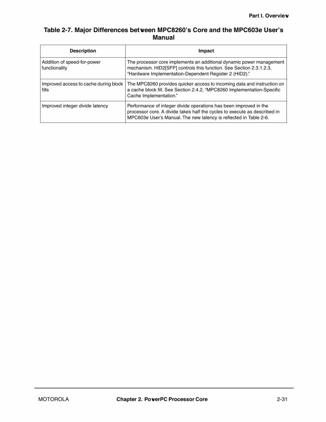
Part I. Overview
Addition of speed-for-power functionality
The processor core implements an additional dynamic power management mechanism. HID2[SFP] controls this function. See Section 2.3.1.2.3, ÒHardware Implementation-Dependent Register 2 (HID2).Ó
Improved access to cache during block Þlls
The MPC8260 provides quicker access to incoming data and instruction on a cache block Þll. See Section 2.4.2, ÒMPC8260 Implementation-SpeciÞc Cache Implementation.Ó
Improved integer divide latency Performance of integer divide operations has been improved in the processor core. A divide takes half the cycles to execute as described in MPC603e UserÕs Manual. The new latency is reßected in Table 2-6.
Table 2-7. Major Differences between MPC8260Õs Core and the MPC603e UserÕs Manual
Description Impact
MOTOROLA Chapter 2. PowerPC Processor Core 2-31

Part I. Overview
2-32 MPC8260 PowerQUICC II UserÕs Manual MOTOROLA
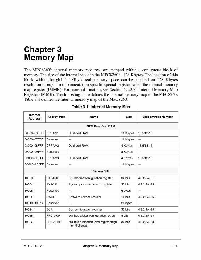
Chapter 3 Memory Map3030
The MPC8260's internal memory resources are mapped within a contiguous block ofmemory. The size of the internal space in the MPC8260 is 128 Kbytes. The location of thisblock within the global 4-Gbyte real memory space can be mapped on 128 Kbytesresolution through an implementation speciÞc special register called the internal memorymap register (IMMR). For more information, see Section 4.3.2.7, ÒInternal Memory MapRegister (IMMR). The following table deÞnes the internal memory map of the MPC8260.Table 3-1 deÞnes the internal memory map of the MPC8260.
Table 3-1. Internal Memory Map
Internal Address
Abbreviation Name Size Section/Page Number
CPM Dual-Port RAM
00000Ð03FFF DPRAM1 Dual-port RAM 16 Kbytes 13.5/13-15
04000Ð07FFF Reserved Ñ 16 Kbytes Ñ
08000Ð08FFF DPRAM2 Dual-port RAM 4 Kbytes 13.5/13-15
09000Ð0AFFF Reserved Ñ 8 Kbytes Ñ
0B000Ð0BFFF DPRAM3 Dual-port RAM 4 Kbytes 13.5/13-15
0C000Ð0FFFF Reserved Ñ 16 Kbytes Ñ
General SIU
10000 SIUMCR SIU module conÞguration register 32 bits 4.3.2.6/4-31
10004 SYPCR System protection control register 32 bits 4.3.2.8/4-35
10008 Reserved Ñ 6 bytes Ñ
1000E SWSR Software service register 16 bits 4.3.2.9/4-36
10010Ð10023 Reserved Ñ 20 bytes Ñ
10024 BCR Bus conÞguration register 32 bits 4.3.2.1/4-25
10028 PPC_ACR 60x bus arbiter conÞguration register 8 bits 4.3.2.2/4-28
1002C PPC ALRH 60x bus arbitration-level register high (Þrst 8 clients)
32 bits 4.3.2.3/4-28
MOTOROLA Chapter 3. Memory Map 3-1
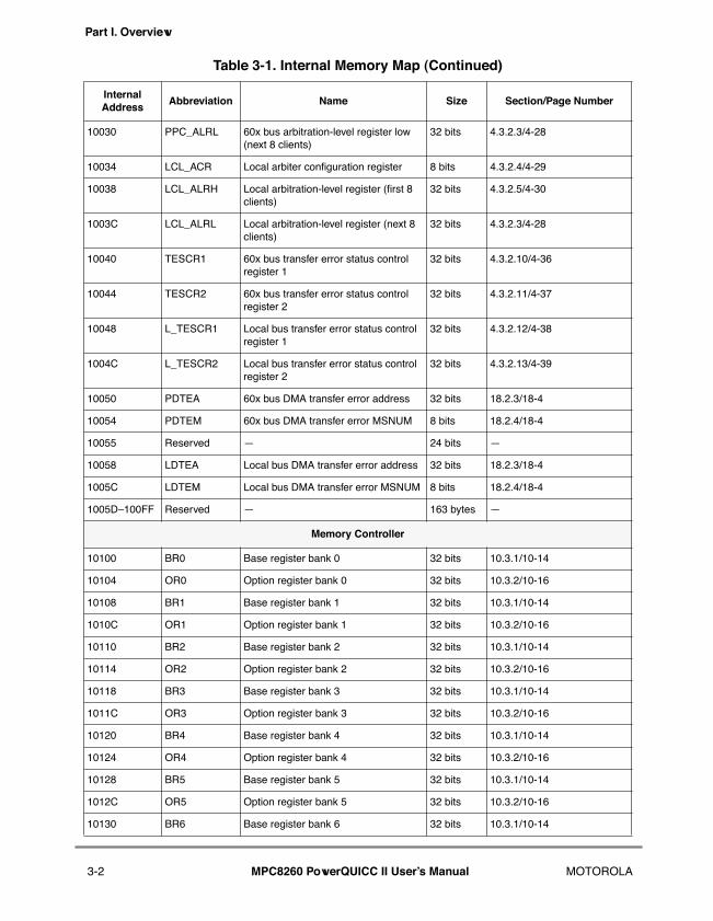
Part I. Overview
10030 PPC_ALRL 60x bus arbitration-level register low (next 8 clients)
32 bits 4.3.2.3/4-28
10034 LCL_ACR Local arbiter conÞguration register 8 bits 4.3.2.4/4-29
10038 LCL_ALRH Local arbitration-level register (Þrst 8 clients)
32 bits 4.3.2.5/4-30
1003C LCL_ALRL Local arbitration-level register (next 8 clients)
32 bits 4.3.2.3/4-28
10040 TESCR1 60x bus transfer error status control register 1
32 bits 4.3.2.10/4-36
10044 TESCR2 60x bus transfer error status control register 2
32 bits 4.3.2.11/4-37
10048 L_TESCR1 Local bus transfer error status control register 1
32 bits 4.3.2.12/4-38
1004C L_TESCR2 Local bus transfer error status control register 2
32 bits 4.3.2.13/4-39
10050 PDTEA 60x bus DMA transfer error address 32 bits 18.2.3/18-4
10054 PDTEM 60x bus DMA transfer error MSNUM 8 bits 18.2.4/18-4
10055 Reserved Ñ 24 bits Ñ
10058 LDTEA Local bus DMA transfer error address 32 bits 18.2.3/18-4
1005C LDTEM Local bus DMA transfer error MSNUM 8 bits 18.2.4/18-4
1005DÐ100FF Reserved Ñ 163 bytes Ñ
Memory Controller
10100 BR0 Base register bank 0 32 bits 10.3.1/10-14
10104 OR0 Option register bank 0 32 bits 10.3.2/10-16
10108 BR1 Base register bank 1 32 bits 10.3.1/10-14
1010C OR1 Option register bank 1 32 bits 10.3.2/10-16
10110 BR2 Base register bank 2 32 bits 10.3.1/10-14
10114 OR2 Option register bank 2 32 bits 10.3.2/10-16
10118 BR3 Base register bank 3 32 bits 10.3.1/10-14
1011C OR3 Option register bank 3 32 bits 10.3.2/10-16
10120 BR4 Base register bank 4 32 bits 10.3.1/10-14
10124 OR4 Option register bank 4 32 bits 10.3.2/10-16
10128 BR5 Base register bank 5 32 bits 10.3.1/10-14
1012C OR5 Option register bank 5 32 bits 10.3.2/10-16
10130 BR6 Base register bank 6 32 bits 10.3.1/10-14
Table 3-1. Internal Memory Map (Continued)
Internal Address
Abbreviation Name Size Section/Page Number
3-2 MPC8260 PowerQUICC II UserÕs Manual MOTOROLA
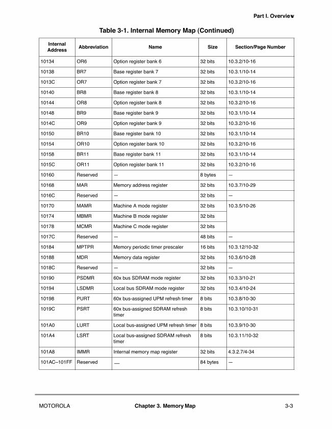
Part I. Overview
10134 OR6 Option register bank 6 32 bits 10.3.2/10-16
10138 BR7 Base register bank 7 32 bits 10.3.1/10-14
1013C OR7 Option register bank 7 32 bits 10.3.2/10-16
10140 BR8 Base register bank 8 32 bits 10.3.1/10-14
10144 OR8 Option register bank 8 32 bits 10.3.2/10-16
10148 BR9 Base register bank 9 32 bits 10.3.1/10-14
1014C OR9 Option register bank 9 32 bits 10.3.2/10-16
10150 BR10 Base register bank 10 32 bits 10.3.1/10-14
10154 OR10 Option register bank 10 32 bits 10.3.2/10-16
10158 BR11 Base register bank 11 32 bits 10.3.1/10-14
1015C OR11 Option register bank 11 32 bits 10.3.2/10-16
10160 Reserved Ñ 8 bytes Ñ
10168 MAR Memory address register 32 bits 10.3.7/10-29
1016C Reserved Ñ 32 bits Ñ
10170 MAMR Machine A mode register 32 bits 10.3.5/10-26
10174 MBMR Machine B mode register 32 bits
10178 MCMR Machine C mode register 32 bits
1017C Reserved Ñ 48 bits Ñ
10184 MPTPR Memory periodic timer prescaler 16 bits 10.3.12/10-32
10188 MDR Memory data register 32 bits 10.3.6/10-28
1018C Reserved Ñ 32 bits Ñ
10190 PSDMR 60x bus SDRAM mode register 32 bits 10.3.3/10-21
10194 LSDMR Local bus SDRAM mode register 32 bits 10.3.4/10-24
10198 PURT 60x bus-assigned UPM refresh timer 8 bits 10.3.8/10-30
1019C PSRT 60x bus-assigned SDRAM refresh timer
8 bits 10.3.10/10-31
101A0 LURT Local bus-assigned UPM refresh timer 8 bits 10.3.9/10-30
101A4 LSRT Local bus-assigned SDRAM refresh timer
8 bits 10.3.11/10-32
101A8 IMMR Internal memory map register 32 bits 4.3.2.7/4-34
101ACÐ101FF Reserved Ñ 84 bytes Ñ
Table 3-1. Internal Memory Map (Continued)
Internal Address
Abbreviation Name Size Section/Page Number
MOTOROLA Chapter 3. Memory Map 3-3
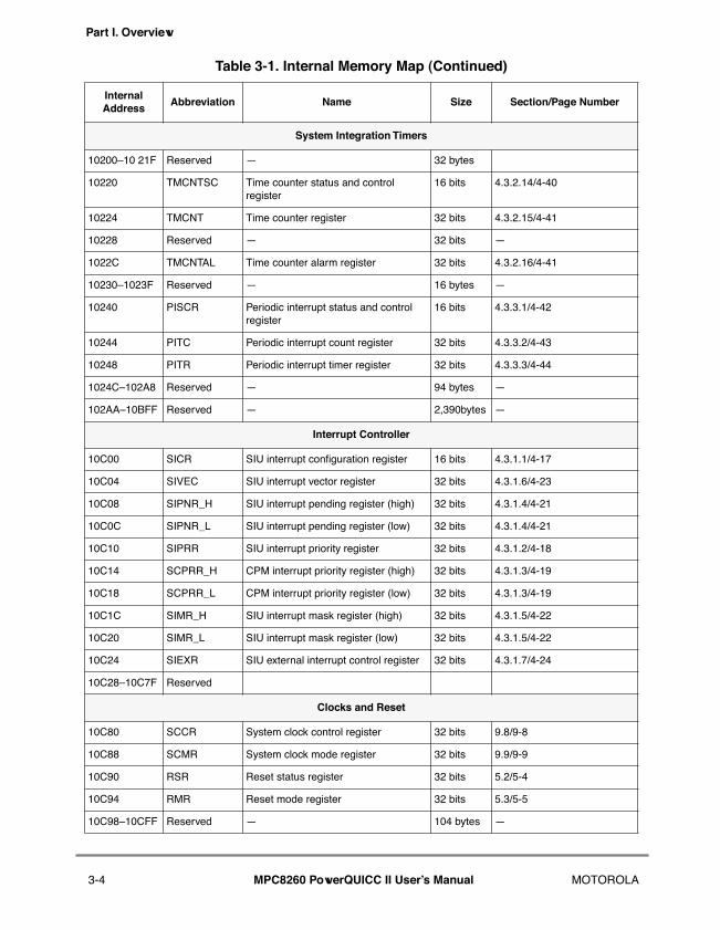
Part I. Overview
System Integration Timers
10200Ð10 21F Reserved Ñ 32 bytes
10220 TMCNTSC Time counter status and control register
16 bits 4.3.2.14/4-40
10224 TMCNT Time counter register 32 bits 4.3.2.15/4-41
10228 Reserved Ñ 32 bits Ñ
1022C TMCNTAL Time counter alarm register 32 bits 4.3.2.16/4-41
10230Ð1023F Reserved Ñ 16 bytes Ñ
10240 PISCR Periodic interrupt status and control register
16 bits 4.3.3.1/4-42
10244 PITC Periodic interrupt count register 32 bits 4.3.3.2/4-43
10248 PITR Periodic interrupt timer register 32 bits 4.3.3.3/4-44
1024CÐ102A8 Reserved Ñ 94 bytes Ñ
102AAÐ10BFF Reserved Ñ 2,390bytes Ñ
Interrupt Controller
10C00 SICR SIU interrupt conÞguration register 16 bits 4.3.1.1/4-17
10C04 SIVEC SIU interrupt vector register 32 bits 4.3.1.6/4-23
10C08 SIPNR_H SIU interrupt pending register (high) 32 bits 4.3.1.4/4-21
10C0C SIPNR_L SIU interrupt pending register (low) 32 bits 4.3.1.4/4-21
10C10 SIPRR SIU interrupt priority register 32 bits 4.3.1.2/4-18
10C14 SCPRR_H CPM interrupt priority register (high) 32 bits 4.3.1.3/4-19
10C18 SCPRR_L CPM interrupt priority register (low) 32 bits 4.3.1.3/4-19
10C1C SIMR_H SIU interrupt mask register (high) 32 bits 4.3.1.5/4-22
10C20 SIMR_L SIU interrupt mask register (low) 32 bits 4.3.1.5/4-22
10C24 SIEXR SIU external interrupt control register 32 bits 4.3.1.7/4-24
10C28Ð10C7F Reserved
Clocks and Reset
10C80 SCCR System clock control register 32 bits 9.8/9-8
10C88 SCMR System clock mode register 32 bits 9.9/9-9
10C90 RSR Reset status register 32 bits 5.2/5-4
10C94 RMR Reset mode register 32 bits 5.3/5-5
10C98Ð10CFF Reserved Ñ 104 bytes Ñ
Table 3-1. Internal Memory Map (Continued)
Internal Address
Abbreviation Name Size Section/Page Number
3-4 MPC8260 PowerQUICC II UserÕs Manual MOTOROLA
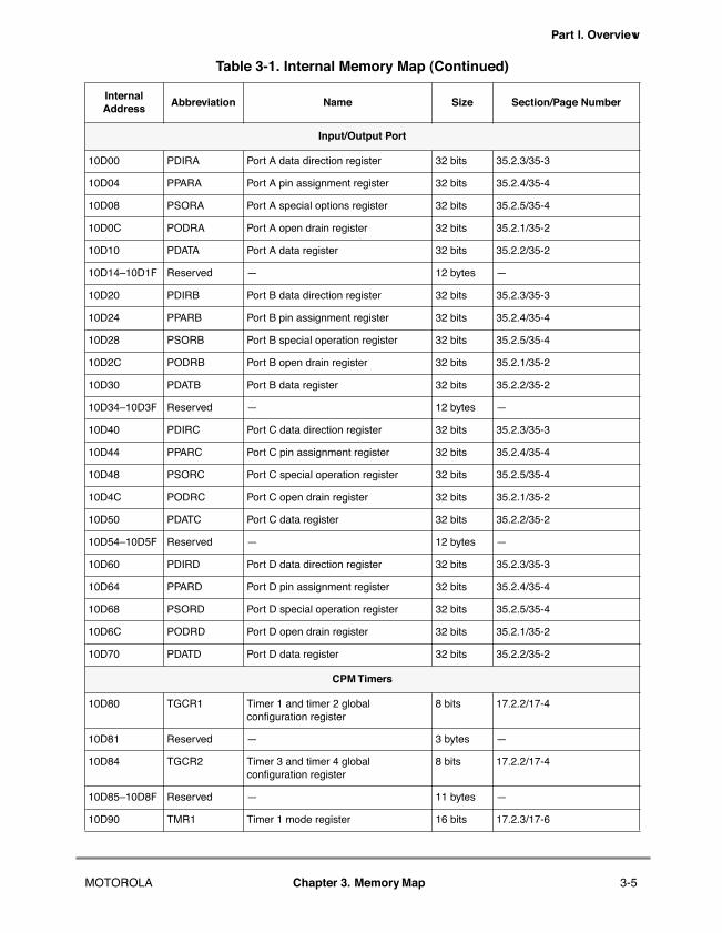
Part I. Overview
Input/Output Port
10D00 PDIRA Port A data direction register 32 bits 35.2.3/35-3
10D04 PPARA Port A pin assignment register 32 bits 35.2.4/35-4
10D08 PSORA Port A special options register 32 bits 35.2.5/35-4
10D0C PODRA Port A open drain register 32 bits 35.2.1/35-2
10D10 PDATA Port A data register 32 bits 35.2.2/35-2
10D14Ð10D1F Reserved Ñ 12 bytes Ñ
10D20 PDIRB Port B data direction register 32 bits 35.2.3/35-3
10D24 PPARB Port B pin assignment register 32 bits 35.2.4/35-4
10D28 PSORB Port B special operation register 32 bits 35.2.5/35-4
10D2C PODRB Port B open drain register 32 bits 35.2.1/35-2
10D30 PDATB Port B data register 32 bits 35.2.2/35-2
10D34Ð10D3F Reserved Ñ 12 bytes Ñ
10D40 PDIRC Port C data direction register 32 bits 35.2.3/35-3
10D44 PPARC Port C pin assignment register 32 bits 35.2.4/35-4
10D48 PSORC Port C special operation register 32 bits 35.2.5/35-4
10D4C PODRC Port C open drain register 32 bits 35.2.1/35-2
10D50 PDATC Port C data register 32 bits 35.2.2/35-2
10D54Ð10D5F Reserved Ñ 12 bytes Ñ
10D60 PDIRD Port D data direction register 32 bits 35.2.3/35-3
10D64 PPARD Port D pin assignment register 32 bits 35.2.4/35-4
10D68 PSORD Port D special operation register 32 bits 35.2.5/35-4
10D6C PODRD Port D open drain register 32 bits 35.2.1/35-2
10D70 PDATD Port D data register 32 bits 35.2.2/35-2
CPM Timers
10D80 TGCR1 Timer 1 and timer 2 global conÞguration register
8 bits 17.2.2/17-4
10D81 Reserved Ñ 3 bytes Ñ
10D84 TGCR2 Timer 3 and timer 4 global conÞguration register
8 bits 17.2.2/17-4
10D85Ð10D8F Reserved Ñ 11 bytes Ñ
10D90 TMR1 Timer 1 mode register 16 bits 17.2.3/17-6
Table 3-1. Internal Memory Map (Continued)
Internal Address
Abbreviation Name Size Section/Page Number
MOTOROLA Chapter 3. Memory Map 3-5
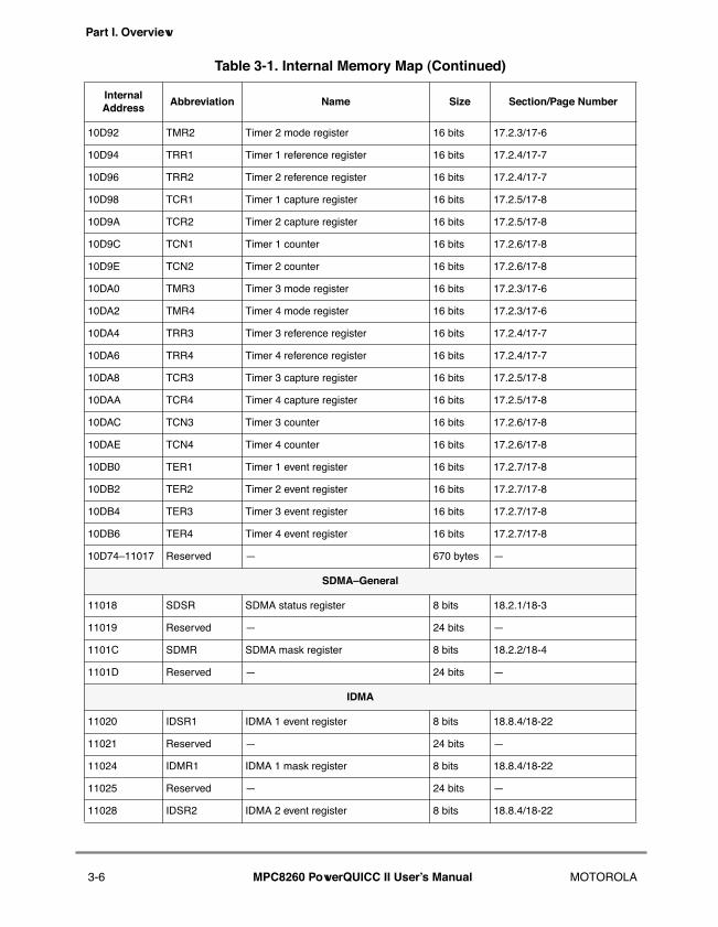
Part I. Overview
10D92 TMR2 Timer 2 mode register 16 bits 17.2.3/17-6
10D94 TRR1 Timer 1 reference register 16 bits 17.2.4/17-7
10D96 TRR2 Timer 2 reference register 16 bits 17.2.4/17-7
10D98 TCR1 Timer 1 capture register 16 bits 17.2.5/17-8
10D9A TCR2 Timer 2 capture register 16 bits 17.2.5/17-8
10D9C TCN1 Timer 1 counter 16 bits 17.2.6/17-8
10D9E TCN2 Timer 2 counter 16 bits 17.2.6/17-8
10DA0 TMR3 Timer 3 mode register 16 bits 17.2.3/17-6
10DA2 TMR4 Timer 4 mode register 16 bits 17.2.3/17-6
10DA4 TRR3 Timer 3 reference register 16 bits 17.2.4/17-7
10DA6 TRR4 Timer 4 reference register 16 bits 17.2.4/17-7
10DA8 TCR3 Timer 3 capture register 16 bits 17.2.5/17-8
10DAA TCR4 Timer 4 capture register 16 bits 17.2.5/17-8
10DAC TCN3 Timer 3 counter 16 bits 17.2.6/17-8
10DAE TCN4 Timer 4 counter 16 bits 17.2.6/17-8
10DB0 TER1 Timer 1 event register 16 bits 17.2.7/17-8
10DB2 TER2 Timer 2 event register 16 bits 17.2.7/17-8
10DB4 TER3 Timer 3 event register 16 bits 17.2.7/17-8
10DB6 TER4 Timer 4 event register 16 bits 17.2.7/17-8
10D74Ð11017 Reserved Ñ 670 bytes Ñ
SDMAÐGeneral
11018 SDSR SDMA status register 8 bits 18.2.1/18-3
11019 Reserved Ñ 24 bits Ñ
1101C SDMR SDMA mask register 8 bits 18.2.2/18-4
1101D Reserved Ñ 24 bits Ñ
IDMA
11020 IDSR1 IDMA 1 event register 8 bits 18.8.4/18-22
11021 Reserved Ñ 24 bits Ñ
11024 IDMR1 IDMA 1 mask register 8 bits 18.8.4/18-22
11025 Reserved Ñ 24 bits Ñ
11028 IDSR2 IDMA 2 event register 8 bits 18.8.4/18-22
Table 3-1. Internal Memory Map (Continued)
Internal Address
Abbreviation Name Size Section/Page Number
3-6 MPC8260 PowerQUICC II UserÕs Manual MOTOROLA
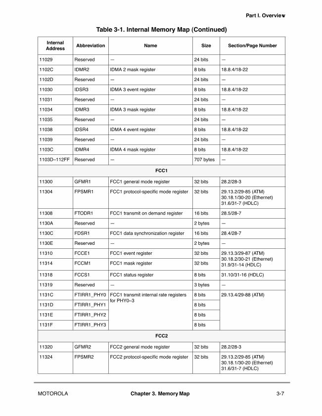
Part I. Overview
11029 Reserved Ñ 24 bits Ñ
1102C IDMR2 IDMA 2 mask register 8 bits 18.8.4/18-22
1102D Reserved Ñ 24 bits Ñ
11030 IDSR3 IDMA 3 event register 8 bits 18.8.4/18-22
11031 Reserved Ñ 24 bits Ñ
11034 IDMR3 IDMA 3 mask register 8 bits 18.8.4/18-22
11035 Reserved Ñ 24 bits Ñ
11038 IDSR4 IDMA 4 event register 8 bits 18.8.4/18-22
11039 Reserved Ñ 24 bits Ñ
1103C IDMR4 IDMA 4 mask register 8 bits 18.8.4/18-22
1103DÐ112FF Reserved Ñ 707 bytes Ñ
FCC1
11300 GFMR1 FCC1 general mode register 32 bits 28.2/28-3
11304 FPSMR1 FCC1 protocol-speciÞc mode register 32 bits 29.13.2/29-85 (ATM)30.18.1/30-20 (Ethernet)31.6/31-7 (HDLC)
11308 FTODR1 FCC1 transmit on demand register 16 bits 28.5/28-7
1130A Reserved Ñ 2 bytes Ñ
1130C FDSR1 FCC1 data synchronization register 16 bits 28.4/28-7
1130E Reserved Ñ 2 bytes Ñ
11310 FCCE1 FCC1 event register 32 bits 29.13.3/29-87 (ATM)30.18.2/30-21 (Ethernet)31.9/31-14 (HDLC)11314 FCCM1 FCC1 mask register 32 bits
11318 FCCS1 FCC1 status register 8 bits 31.10/31-16 (HDLC)
11319 Reserved Ñ 3 bytes Ñ
1131C FTIRR1_PHY0 FCC1 transmit internal rate registers for PHY0Ð3
8 bits 29.13.4/29-88 (ATM)
1131D FTIRR1_PHY1 8 bits
1131E FTIRR1_PHY2 8 bits
1131F FTIRR1_PHY3 8 bits
FCC2
11320 GFMR2 FCC2 general mode register 32 bits 28.2/28-3
11324 FPSMR2 FCC2 protocol-speciÞc mode register 32 bits 29.13.2/29-85 (ATM)30.18.1/30-20 (Ethernet)31.6/31-7 (HDLC)
Table 3-1. Internal Memory Map (Continued)
Internal Address
Abbreviation Name Size Section/Page Number
MOTOROLA Chapter 3. Memory Map 3-7
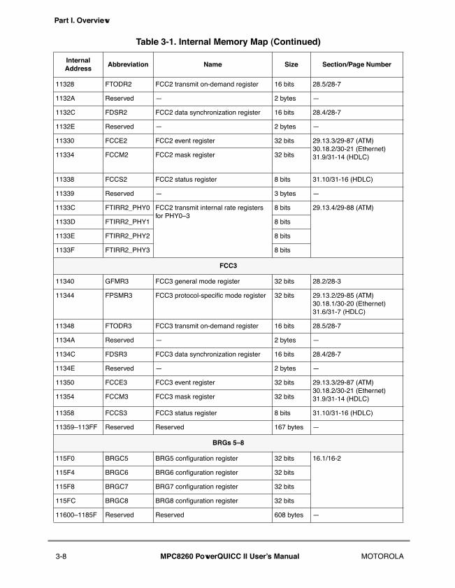
Part I. Overview
11328 FTODR2 FCC2 transmit on-demand register 16 bits 28.5/28-7
1132A Reserved Ñ 2 bytes Ñ
1132C FDSR2 FCC2 data synchronization register 16 bits 28.4/28-7
1132E Reserved Ñ 2 bytes Ñ
11330 FCCE2 FCC2 event register 32 bits 29.13.3/29-87 (ATM)30.18.2/30-21 (Ethernet)31.9/31-14 (HDLC)11334 FCCM2 FCC2 mask register 32 bits
11338 FCCS2 FCC2 status register 8 bits 31.10/31-16 (HDLC)
11339 Reserved Ñ 3 bytes Ñ
1133C FTIRR2_PHY0 FCC2 transmit internal rate registers for PHY0Ð3
8 bits 29.13.4/29-88 (ATM)
1133D FTIRR2_PHY1 8 bits
1133E FTIRR2_PHY2 8 bits
1133F FTIRR2_PHY3 8 bits
FCC3
11340 GFMR3 FCC3 general mode register 32 bits 28.2/28-3
11344 FPSMR3 FCC3 protocol-speciÞc mode register 32 bits 29.13.2/29-85 (ATM)30.18.1/30-20 (Ethernet)31.6/31-7 (HDLC)
11348 FTODR3 FCC3 transmit on-demand register 16 bits 28.5/28-7
1134A Reserved Ñ 2 bytes Ñ
1134C FDSR3 FCC3 data synchronization register 16 bits 28.4/28-7
1134E Reserved Ñ 2 bytes Ñ
11350 FCCE3 FCC3 event register 32 bits 29.13.3/29-87 (ATM)30.18.2/30-21 (Ethernet)31.9/31-14 (HDLC)11354 FCCM3 FCC3 mask register 32 bits
11358 FCCS3 FCC3 status register 8 bits 31.10/31-16 (HDLC)
11359Ð113FF Reserved Reserved 167 bytes Ñ
BRGs 5Ð8
115F0 BRGC5 BRG5 conÞguration register 32 bits 16.1/16-2
115F4 BRGC6 BRG6 conÞguration register 32 bits
115F8 BRGC7 BRG7 conÞguration register 32 bits
115FC BRGC8 BRG8 conÞguration register 32 bits
11600Ð1185F Reserved Reserved 608 bytes Ñ
Table 3-1. Internal Memory Map (Continued)
Internal Address
Abbreviation Name Size Section/Page Number
3-8 MPC8260 PowerQUICC II UserÕs Manual MOTOROLA
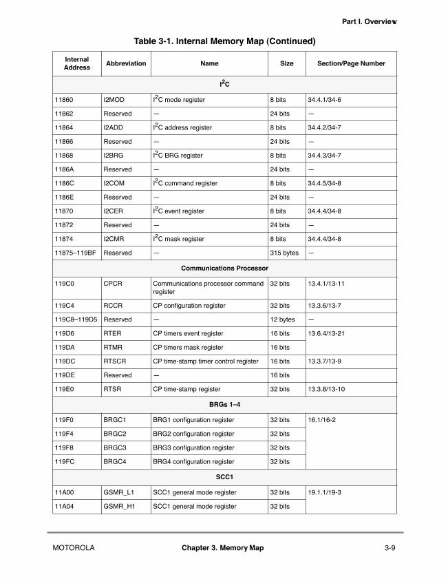
Part I. Overview
I2C
11860 I2MOD I2C mode register 8 bits 34.4.1/34-6
11862 Reserved Ñ 24 bits Ñ
11864 I2ADD I2C address register 8 bits 34.4.2/34-7
11866 Reserved Ñ 24 bits Ñ
11868 I2BRG I2C BRG register 8 bits 34.4.3/34-7
1186A Reserved Ñ 24 bits Ñ
1186C I2COM I2C command register 8 bits 34.4.5/34-8
1186E Reserved Ñ 24 bits Ñ
11870 I2CER I2C event register 8 bits 34.4.4/34-8
11872 Reserved Ñ 24 bits Ñ
11874 I2CMR I2C mask register 8 bits 34.4.4/34-8
11875Ð119BF Reserved Ñ 315 bytes Ñ
Communications Processor
119C0 CPCR Communications processor command register
32 bits 13.4.1/13-11
119C4 RCCR CP conÞguration register 32 bits 13.3.6/13-7
119C8Ð119D5 Reserved Ñ 12 bytes Ñ
119D6 RTER CP timers event register 16 bits 13.6.4/13-21
119DA RTMR CP timers mask register 16 bits
119DC RTSCR CP time-stamp timer control register 16 bits 13.3.7/13-9
119DE Reserved Ñ 16 bits
119E0 RTSR CP time-stamp register 32 bits 13.3.8/13-10
BRGs 1Ð4
119F0 BRGC1 BRG1 conÞguration register 32 bits 16.1/16-2
119F4 BRGC2 BRG2 conÞguration register 32 bits
119F8 BRGC3 BRG3 conÞguration register 32 bits
119FC BRGC4 BRG4 conÞguration register 32 bits
SCC1
11A00 GSMR_L1 SCC1 general mode register 32 bits 19.1.1/19-3
11A04 GSMR_H1 SCC1 general mode register 32 bits
Table 3-1. Internal Memory Map (Continued)
Internal Address
Abbreviation Name Size Section/Page Number
MOTOROLA Chapter 3. Memory Map 3-9
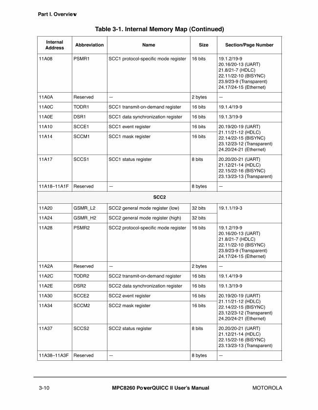
Part I. Overview
11A08 PSMR1 SCC1 protocol-speciÞc mode register 16 bits 19.1.2/19-920.16/20-13 (UART)21.8/21-7 (HDLC)22.11/22-10 (BISYNC)23.9/23-9 (Transparent)24.17/24-15 (Ethernet)
11A0A Reserved Ñ 2 bytes Ñ
11A0C TODR1 SCC1 transmit-on-demand register 16 bits 19.1.4/19-9
11A0E DSR1 SCC1 data synchronization register 16 bits 19.1.3/19-9
11A10 SCCE1 SCC1 event register 16 bits 20.19/20-19 (UART)21.11/21-12 (HDLC)22.14/22-15 (BISYNC)23.12/23-12 (Transparent)24.20/24-21 (Ethernet)
11A14 SCCM1 SCC1 mask register 16 bits
11A17 SCCS1 SCC1 status register 8 bits 20.20/20-21 (UART)21.12/21-14 (HDLC)22.15/22-16 (BISYNC)23.13/23-13 (Transparent)
11A18Ð11A1F Reserved Ñ 8 bytes Ñ
SCC2
11A20 GSMR_L2 SCC2 general mode register (low) 32 bits 19.1.1/19-3
11A24 GSMR_H2 SCC2 general mode register (high) 32 bits
11A28 PSMR2 SCC2 protocol-speciÞc mode register 16 bits 19.1.2/19-920.16/20-13 (UART)21.8/21-7 (HDLC)22.11/22-10 (BISYNC)23.9/23-9 (Transparent)24.17/24-15 (Ethernet)
11A2A Reserved Ñ 2 bytes Ñ
11A2C TODR2 SCC2 transmit-on-demand register 16 bits 19.1.4/19-9
11A2E DSR2 SCC2 data synchronization register 16 bits 19.1.3/19-9
11A30 SCCE2 SCC2 event register 16 bits 20.19/20-19 (UART)21.11/21-12 (HDLC)22.14/22-15 (BISYNC)23.12/23-12 (Transparent)24.20/24-21 (Ethernet)
11A34 SCCM2 SCC2 mask register 16 bits
11A37 SCCS2 SCC2 status register 8 bits 20.20/20-21 (UART)21.12/21-14 (HDLC)22.15/22-16 (BISYNC)23.13/23-13 (Transparent)
11A38Ð11A3F Reserved Ñ 8 bytes Ñ
Table 3-1. Internal Memory Map (Continued)
Internal Address
Abbreviation Name Size Section/Page Number
3-10 MPC8260 PowerQUICC II UserÕs Manual MOTOROLA
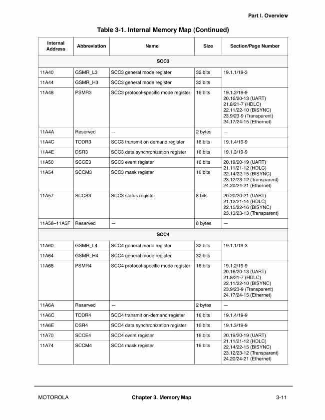
Part I. Overview
SCC3
11A40 GSMR_L3 SCC3 general mode register 32 bits 19.1.1/19-3
11A44 GSMR_H3 SCC3 general mode register 32 bits
11A48 PSMR3 SCC3 protocol-speciÞc mode register 16 bits 19.1.2/19-920.16/20-13 (UART)21.8/21-7 (HDLC)22.11/22-10 (BISYNC)23.9/23-9 (Transparent)24.17/24-15 (Ethernet)
11A4A Reserved Ñ 2 bytes Ñ
11A4C TODR3 SCC3 transmit on demand register 16 bits 19.1.4/19-9
11A4E DSR3 SCC3 data synchronization register 16 bits 19.1.3/19-9
11A50 SCCE3 SCC3 event register 16 bits 20.19/20-19 (UART)21.11/21-12 (HDLC)22.14/22-15 (BISYNC)23.12/23-12 (Transparent)24.20/24-21 (Ethernet)
11A54 SCCM3 SCC3 mask register 16 bits
11A57 SCCS3 SCC3 status register 8 bits 20.20/20-21 (UART)21.12/21-14 (HDLC)22.15/22-16 (BISYNC)23.13/23-13 (Transparent)
11A58Ð11A5F Reserved Ñ 8 bytes Ñ
SCC4
11A60 GSMR_L4 SCC4 general mode register 32 bits 19.1.1/19-3
11A64 GSMR_H4 SCC4 general mode register 32 bits
11A68 PSMR4 SCC4 protocol-speciÞc mode register 16 bits 19.1.2/19-920.16/20-13 (UART)21.8/21-7 (HDLC)22.11/22-10 (BISYNC)23.9/23-9 (Transparent)24.17/24-15 (Ethernet)
11A6A Reserved Ñ 2 bytes Ñ
11A6C TODR4 SCC4 transmit on-demand register 16 bits 19.1.4/19-9
11A6E DSR4 SCC4 data synchronization register 16 bits 19.1.3/19-9
11A70 SCCE4 SCC4 event register 16 bits 20.19/20-19 (UART)21.11/21-12 (HDLC)22.14/22-15 (BISYNC)23.12/23-12 (Transparent)24.20/24-21 (Ethernet)
11A74 SCCM4 SCC4 mask register 16 bits
Table 3-1. Internal Memory Map (Continued)
Internal Address
Abbreviation Name Size Section/Page Number
MOTOROLA Chapter 3. Memory Map 3-11
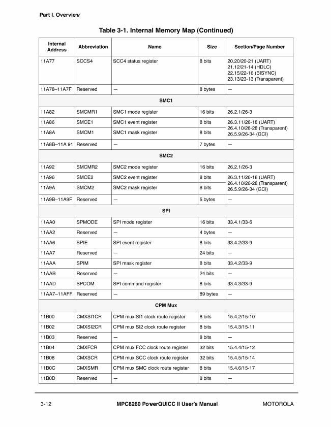
Part I. Overview
11A77 SCCS4 SCC4 status register 8 bits 20.20/20-21 (UART)21.12/21-14 (HDLC)22.15/22-16 (BISYNC)23.13/23-13 (Transparent)
11A78Ð11A7F Reserved Ñ 8 bytes Ñ
SMC1
11A82 SMCMR1 SMC1 mode register 16 bits 26.2.1/26-3
11A86 SMCE1 SMC1 event register 8 bits 26.3.11/26-18 (UART)26.4.10/26-28 (Transparent)26.5.9/26-34 (GCI)11A8A SMCM1 SMC1 mask register 8 bits
11A8BÐ11A 91 Reserved Ñ 7 bytes Ñ
SMC2
11A92 SMCMR2 SMC2 mode register 16 bits 26.2.1/26-3
11A96 SMCE2 SMC2 event register 8 bits 26.3.11/26-18 (UART)26.4.10/26-28 (Transparent)26.5.9/26-34 (GCI)11A9A SMCM2 SMC2 mask register 8 bits
11A9BÐ11A9F Reserved Ñ 5 bytes Ñ
SPI
11AA0 SPMODE SPI mode register 16 bits 33.4.1/33-6
11AA2 Reserved Ñ 4 bytes Ñ
11AA6 SPIE SPI event register 8 bits 33.4.2/33-9
11AA7 Reserved Ñ 24 bits Ñ
11AAA SPIM SPI mask register 8 bits 33.4.2/33-9
11AAB Reserved Ñ 24 bits Ñ
11AAD SPCOM SPI command register 8 bits 33.4.3/33-9
11AA7Ð11AFF Reserved Ñ 89 bytes Ñ
CPM Mux
11B00 CMXSI1CR CPM mux SI1 clock route register 8 bits 15.4.2/15-10
11B02 CMXSI2CR CPM mux SI2 clock route register 8 bits 15.4.3/15-11
11B03 Reserved Ñ 8 bits Ñ
11B04 CMXFCR CPM mux FCC clock route register 32 bits 15.4.4/15-12
11B08 CMXSCR CPM mux SCC clock route register 32 bits 15.4.5/15-14
11B0C CMXSMR CPM mux SMC clock route register 8 bits 15.4.6/15-17
11B0D Reserved Ñ 8 bits Ñ
Table 3-1. Internal Memory Map (Continued)
Internal Address
Abbreviation Name Size Section/Page Number
3-12 MPC8260 PowerQUICC II UserÕs Manual MOTOROLA
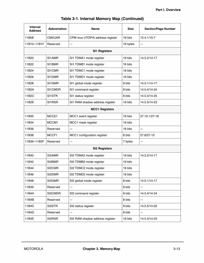
Part I. Overview
11B0E CMXUAR CPM mux UTOPIA address register 16 bits 15.4.1/15-7
11B10Ð11B1F Reserved Ñ 16 bytes Ñ
SI1 Registers
11B20 SI1AMR SI1 TDMA1 mode register 16 bits 14.5.2/14-17
11B22 SI1BMR SI1 TDMB1 mode register 16 bits
11B24 SI1CMR SI1 TDMC1 mode register 16 bits
11B26 SI1DMR SI1 TDMD1 mode register 16 bits
11B28 SI1GMR SI1 global mode register 8 bits 14.5.1/14-17
11B2A SI1CMDR SI1 command register 8 bits 14.5.4/14-24
11B2C SI1STR SI1 status register 8 bits 14.5.5/14-25
11B2E SI1RSR SI1 RAM shadow address register 16 bits 14.5.3/14-23
MCC1 Registers
11B30 MCCE1 MCC1 event register 16 bits 27.10.1/27-18
11B34 MCCM1 MCC1 mask register 16 bits
11B36 Reserved Ñ 16 bits Ñ
11B38 MCCF1 MCC1 conÞguration register 8 bits 27.8/27-15
11B39Ð11B3F Reserved Ñ 7 bytes Ñ
SI2 Registers
11B40 SI2AMR SI2 TDMA2 mode register 16 bits 14.5.2/14-17
11B42 SI2BMR SI2 TDMB2 mode register 16 bits
11B44 SI2CMR SI2 TDMC2 mode register 16 bits
11B46 SI2DMR SI2 TDMD2 mode register 16 bits
11B48 SI2GMR SI2 global mode register 8 bits 14.5.1/14-17
11B49 Reserved Ñ 8 bits Ñ
11B4A SI2CMDR SI2 command register 8 bits 14.5.4/14-24
11B4B Reserved Ñ 8 bits Ñ
11B4C SI2STR SI2 status register 8 bits 14.5.5/14-25
11B4D Reserved Ñ 8 bits Ñ
11B4E SI2RSR SI2 RAM shadow address register 16 bits 14.5.3/14-23
Table 3-1. Internal Memory Map (Continued)
Internal Address
Abbreviation Name Size Section/Page Number
MOTOROLA Chapter 3. Memory Map 3-13
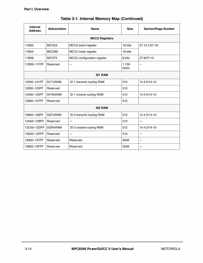
Part I. Overview
MCC2 Registers
11B50 MCCE2 MCC2 event register 16 bits 27.10.1/27-18
11B54 MCCM2 MCC2 mask register 16 bits
11B58 MCCF2 MCC2 conÞguration register 8 bits 27.8/27-15
11B59Ð11FFF Reserved Ñ 1,159 bytes
Ñ
SI1 RAM
12000Ð121FF SI1TxRAM SI 1 transmit routing RAM 512 14.4.3/14-10
12200Ð123FF Reserved 512
12400Ð125FF SI1RxRAM SI 1 receive routing RAM 512 14.4.3/14-10
12600Ð127FF Reserved 512
SI2 RAM
12800Ð129FF SI2TxRAM SI 2 transmit routing RAM 512 14.4.3/14-10
12A00Ð12BFF Reserved Ñ 512 Ñ
12C00Ð12DFF SI2RxRAM SI 2 receive routing RAM 512 14.4.3/14-10
12E00Ð12FFF Reserved Ñ 512 Ñ
13000Ð137FF Reserved Reserved 2048 Ñ
13800Ð13FFF Reserved Reserved 2048 Ñ
Table 3-1. Internal Memory Map (Continued)
Internal Address
Abbreviation Name Size Section/Page Number
3-14 MPC8260 PowerQUICC II UserÕs Manual MOTOROLA
Part IIConÞguration and Reset
AudiencePart II is intended for system designers and programmers who need to understand theoperation of the MPC8260 at start up. It assumes understanding of the PowerPCprogramming model described in the previous chapters and a high level understanding ofthe MPC8260.
ContentsPart II describes start-up behavior of the MPC8260.
It contains the following chapters:
¥ Chapter 4, ÒSystem Interface Unit (SIU),Ó describes the system conÞguration and protection functions which provide various monitors and timers, and the 60x bus conÞguration.
¥ Chapter 5, ÒReset,Ó describes the behavior of the MPC8260 at reset and start-up.
Suggested ReadingSupporting documentation for the MPC8260 can be accessed through the world-wide webat http://www.motorola.com/netcomm and at http://www.mot.com/PowerPC. Thisdocumentation includes technical speciÞcations, reference materials, and detailedapplications notes.
MOTOROLA Part II. Configuration and Reset Part II-i
Part II. Configuration and Reset
ConventionsThis chapter uses the following notational conventions:
Bold entries in Þgures and tables showing registers and parameter RAM should be initialized by the user.
mnemonics Instruction mnemonics are shown in lowercase bold.
italics Italics indicate variable command parameters, for example, bcctrx.Book titles in text are set in italics.
0x0 PreÞx to denote hexadecimal number
0b0 PreÞx to denote binary number
rA, rB Instruction syntax used to identify a source GPR
rD Instruction syntax used to identify a destination GPR
REG[FIELD] Abbreviations or acronyms for registers or buffer descriptors are shown in uppercase text. SpeciÞc bits, Þelds, or numerical ranges appear in brackets. For example, MSR[LE] refers to the little-endian mode enable bit in the machine state register.
x In certain contexts, such as in a signal encoding or a bit Þeld, indicates a donÕt care.
n Indicates an undeÞned numerical value
Acronyms and AbbreviationsTable i contains acronyms and abbreviations that are used in this document. Note that themeanings for some acronyms (such as SDR1 and DSISR) are historical, and the words forwhich an acronym stands may not be intuitively obvious.
Table v. Acronyms and Abbreviated Terms
Term Meaning
BIST Built-in self test
DMA Direct memory access
DRAM Dynamic random access memory
EA Effective address
GPR General-purpose register
IEEE Institute of Electrical and Electronics Engineers
LSB Least-signiÞcant byte
lsb Least-signiÞcant bit
LSU Load/store unit
MSB Most-signiÞcant byte
Bold
Part II-ii MPC8260 PowerQUICC II UserÕs Manual MOTOROLA
Part II. Configuration and Reset
msb Most-signiÞcant bit
MSR Machine state register
PCI Peripheral component interconnect
RTOS Real-time operating system
Rx Receive
SPR Special-purpose register
SWT Software watchdog timer
Tx Transmit
Table v. Acronyms and Abbreviated Terms (Continued)
Term Meaning
MOTOROLA Part II. Configuration and Reset Part II-iii

Part II. Configuration and Reset
Part II-iv MPC8260 PowerQUICC II UserÕs Manual MOTOROLA
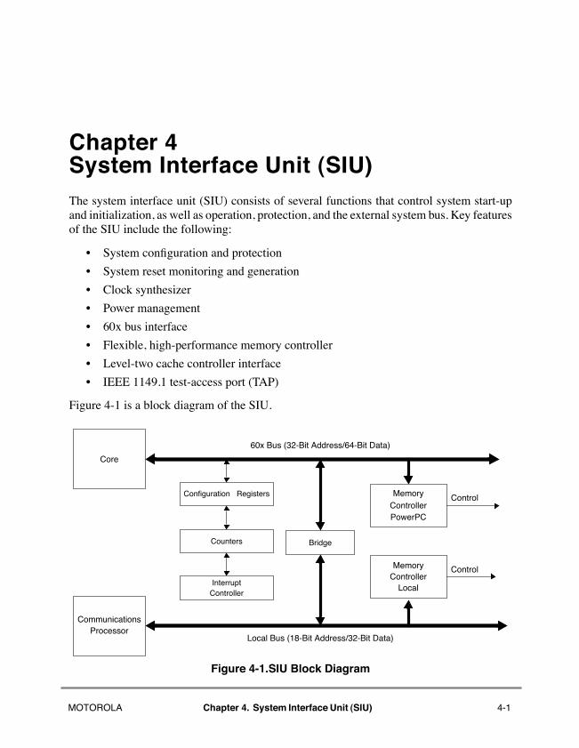
Chapter 4 System Interface Unit (SIU)4040
The system interface unit (SIU) consists of several functions that control system start-upand initialization, as well as operation, protection, and the external system bus. Key featuresof the SIU include the following:
¥ System conÞguration and protection
¥ System reset monitoring and generation
¥ Clock synthesizer
¥ Power management
¥ 60x bus interface
¥ Flexible, high-performance memory controller
¥ Level-two cache controller interface
¥ IEEE 1149.1 test-access port (TAP)
Figure 4-1 is a block diagram of the SIU.
Figure 4-1.SIU Block Diagram
60x Bus (32-Bit Address/64-Bit Data)
MemoryControllerPowerPC
Control
MemoryController
Local
Control
Local Bus (18-Bit Address/32-Bit Data)
Bridge
Core
CommunicationsProcessor
Configuration Registers
Counters
InterruptController
MOTOROLA Chapter 4. System Interface Unit (SIU) 4-1
Part II. ConÞguration and Reset
The system conÞguration and protection functions provide various monitors and timers,including the bus monitor, software watchdog timer, periodic interrupt timer, and timecounter. The clock synthesizer generates the clock signals used by the SIU and otherMPC8260 modules. The SIU clocking scheme supports stop and normal modes.
The 60x bus interface is a standard pipelined bus. The MPC8260 allows external busmasters to request and obtain system bus mastership. Chapter 8, ÒThe 60x Bus,Ó describesbus operation, but 60x bus conÞguration is explained in this section.
The memory controller module, described in Chapter 10, ÒMemory Controller,Ó provides aseamless interface to many types of memory devices and peripherals. It supports up totwelve memory banks, each with its own device and timing attributes.
The MPC8260Õs implementation supports circuit board test strategies through a user-accessible test logic that is fully compliant with the IEEE 1149.1 test access port.
4.1 System ConÞguration and ProtectionThe MPC8260 incorporates many system functions that normally must be provided inexternal circuits. In addition, it is designed to provide maximum system safeguards againsthardware and/or software faults. Table 4-1 describes functions provided in the systemconÞguration and protection submodule.
Table 4-1. System Configuration and Protection Functions
Function Description
System conÞguration
The SIU allows the user to conÞgure the system according to the particular requirements. The functions include control of parity checking and part and mask number constants.
60x bus monitor
Monitors the transfer acknowledge (TA) and address acknowledge (AACK) response time for all bus accesses initiated by internal or external masters. TEA is asserted if the TA/AACK response limit is exceeded. This function can be disabled if needed.
Local bus monitor
Monitors transfers between local bus internal masters and local bus slaves. An internal TEA assertion occurs if the transfer time limit is exceeded. This function can be disabled.
Software watchdog timer
Asserts a reset or NMI interrupt, selected by the system protection control register (SYPCR) if the software fails to service the software watchdog timer for a certain period of time (for example, because software is lost or trapped in a loop). After a system reset, this function is enabled, selects a maximum time-out period, and asserts a system reset if the time-out is reached. The software watchdog timer can be disabled or its time-out period may be changed in the SYPCR. Once the SYPCR is written, it cannot be written again until a system reset. For more information, see Section 4.1.5, ÒSoftware Watchdog Timer.Ó
Periodic interrupt timer (PIT)
Generates periodic interrupts for use with a real-time operating system or the application software. The periodic interrupt timer (PIT) is clocked by the timersclk clock, providing a period from 122 µs to 8 seconds. The PIT function can be disabled if needed. See Section 4.1.4, ÒPeriodic Interrupt Timer (PIT).Ó
Time counter
Provides a time-of-day information to the operating system/application software. It is composed of a 45-bit counter and an alarm register. A maskable interrupt is generated when the counter reaches the value programmed in the alarm register. The time counter (TMCNT) is clocked by the timersclk clock. See Section 4.1.3, ÒTime Counter (TMCNT).Ó
4-2 MPC8260 PowerQUICC II UserÕs Manual MOTOROLA
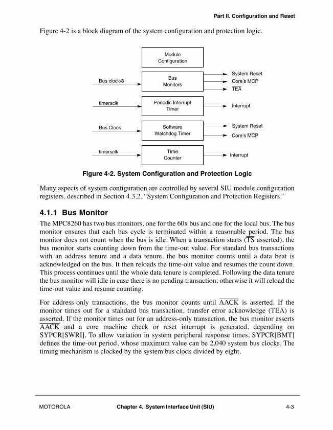
Part II. ConÞguration and Reset
Figure 4-2 is a block diagram of the system conÞguration and protection logic.
Figure 4-2. System Configuration and Protection Logic
Many aspects of system conÞguration are controlled by several SIU module conÞgurationregisters, described in Section 4.3.2, ÒSystem ConÞguration and Protection Registers.Ó
4.1.1 Bus MonitorThe MPC8260 has two bus monitors, one for the 60x bus and one for the local bus. The busmonitor ensures that each bus cycle is terminated within a reasonable period. The busmonitor does not count when the bus is idle. When a transaction starts (TS asserted), thebus monitor starts counting down from the time-out value. For standard bus transactionswith an address tenure and a data tenure, the bus monitor counts until a data beat isacknowledged on the bus. It then reloads the time-out value and resumes the count down.This process continues until the whole data tenure is completed. Following the data tenurethe bus monitor will idle in case there is no pending transaction; otherwise it will reload thetime-out value and resume counting.
For address-only transactions, the bus monitor counts until AACK is asserted. If themonitor times out for a standard bus transaction, transfer error acknowledge (TEA) isasserted. If the monitor times out for an address-only transaction, the bus monitor assertsAACK and a core machine check or reset interrupt is generated, depending onSYPCR[SWRI]. To allow variation in system peripheral response times, SYPCR[BMT]deÞnes the time-out period, whose maximum value can be 2,040 system bus clocks. Thetiming mechanism is clocked by the system bus clock divided by eight.
ModuleConfiguration
BusMonitors
Periodic InterruptTimer
SoftwareWatchdog Timer
TimeCounter
TEA
Interrupt
CoreÕs MCP
Interrupt
CoreÕs MCP
System Reset
timersclk
Bus Clock
timersclk
System Reset
Bus clock/8
MOTOROLA Chapter 4. System Interface Unit (SIU) 4-3
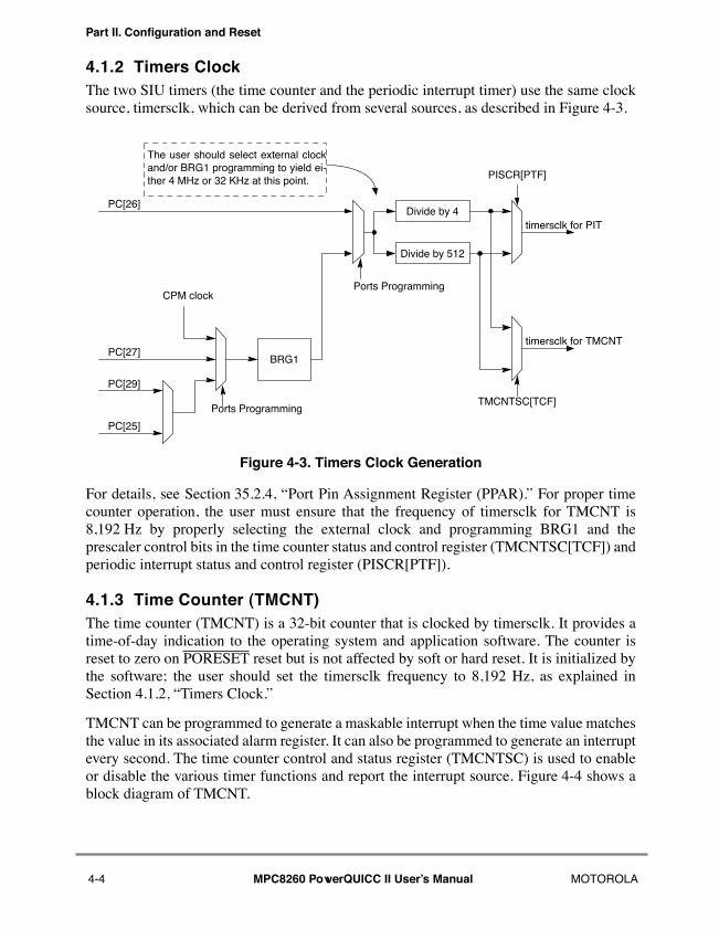
Part II. ConÞguration and Reset
4.1.2 Timers ClockThe two SIU timers (the time counter and the periodic interrupt timer) use the same clocksource, timersclk, which can be derived from several sources, as described in Figure 4-3.
Figure 4-3. Timers Clock Generation
For details, see Section 35.2.4, ÒPort Pin Assignment Register (PPAR).Ó For proper timecounter operation, the user must ensure that the frequency of timersclk for TMCNT is8,192 Hz by properly selecting the external clock and programming BRG1 and theprescaler control bits in the time counter status and control register (TMCNTSC[TCF]) andperiodic interrupt status and control register (PISCR[PTF]).
4.1.3 Time Counter (TMCNT)The time counter (TMCNT) is a 32-bit counter that is clocked by timersclk. It provides atime-of-day indication to the operating system and application software. The counter isreset to zero on PORESET reset but is not affected by soft or hard reset. It is initialized bythe software; the user should set the timersclk frequency to 8,192 Hz, as explained inSection 4.1.2, ÒTimers Clock.Ó
TMCNT can be programmed to generate a maskable interrupt when the time value matchesthe value in its associated alarm register. It can also be programmed to generate an interruptevery second. The time counter control and status register (TMCNTSC) is used to enableor disable the various timer functions and report the interrupt source. Figure 4-4 shows ablock diagram of TMCNT.
PC[29]
PC[25]
CPM clock
PC[27]
PC[26]
Ports Programming
The user should select external clockand/or BRG1 programming to yield ei-ther 4 MHz or 32 KHz at this point.
BRG1
Divide by 512
Divide by 4
PISCR[PTF]
TMCNTSC[TCF]
Ports Programming
timersclk for TMCNT
timersclk for PIT
4-4 MPC8260 PowerQUICC II UserÕs Manual MOTOROLA
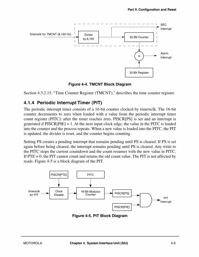
Part II. ConÞguration and Reset
Figure 4-4. TMCNT Block Diagram
Section 4.3.2.15, ÒTime Counter Register (TMCNT),Ó describes the time counter register.
4.1.4 Periodic Interrupt Timer (PIT)The periodic interrupt timer consists of a 16-bit counter clocked by timersclk. The 16-bitcounter decrements to zero when loaded with a value from the periodic interrupt timercount register (PITC); after the timer reaches zero, PISCR[PS] is set and an interrupt isgenerated if PISCR[PIE] = 1. At the next input clock edge, the value in the PITC is loadedinto the counter and the process repeats. When a new value is loaded into the PITC, the PITis updated, the divider is reset, and the counter begins counting.
Setting PS creates a pending interrupt that remains pending until PS is cleared. If PS is setagain before being cleared, the interrupt remains pending until PS is cleared. Any write tothe PITC stops the current countdown and the count resumes with the new value in PITC.If PTE = 0, the PIT cannot count and retains the old count value. The PIT is not affected byreads. Figure 4-5 is a block diagram of the PIT.
Figure 4-5. PIT Block Diagram
Divide32-Bit Counter
32-Bit Register
SEC
Alarm= Interrupt
Interrupt
by 8,192
timersclk for TMCNT (8,192 Hz)
Clock
PITC
timersclkPISCR[PS]
PISCR[PIE]
PIT
PISCR[PTE]
Disablefor PIT16-Bit Modulus
Interrupt
Counter
MOTOROLA Chapter 4. System Interface Unit (SIU) 4-5
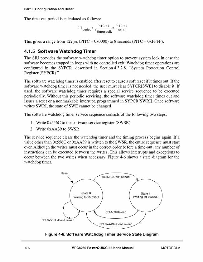
Part II. ConÞguration and Reset
The time-out period is calculated as follows:
This gives a range from 122 µs (PITC = 0x0000) to 8 seconds (PITC = 0xFFFF).
4.1.5 Software Watchdog Timer The SIU provides the software watchdog timer option to prevent system lock in case thesoftware becomes trapped in loops with no controlled exit. Watchdog timer operations areconÞgured in the SYPCR, described in Section 4.3.2.8, ÒSystem Protection ControlRegister (SYPCR).Ó
The software watchdog timer is enabled after reset to cause a soft reset if it times out. If thesoftware watchdog timer is not needed, the user must clear SYPCR[SWE] to disable it. Ifused, the software watchdog timer requires a special service sequence to be executedperiodically. Without this periodic servicing, the software watchdog timer times out andissues a reset or a nonmaskable interrupt, programmed in SYPCR[SWRI]. Once softwarewrites SWRI, the state of SWE cannot be changed.
The software watchdog timer service sequence consists of the following two steps:
1. Write 0x556C to the software service register (SWSR)
2. Write 0xAA39 to SWSR
The service sequence clears the watchdog timer and the timing process begins again. If avalue other than 0x556C or 0xAA39 is written to the SWSR, the entire sequence must startover. Although the writes must occur in the correct order before a time-out, any number ofinstructions can be executed between the writes. This allows interrupts and exceptions tooccur between the two writes when necessary. Figure 4-6 shows a state diagram for thewatchdog timer.
Figure 4-6. Software Watchdog Timer Service State Diagram
PIT periodPITC 1+
F timersclk-------------------------------------
PITC 1+8192
-------------------------==
0x556C/DonÕt reloadReset
0xAA39/Reload
State 0Waiting for 0x556C
State 1Waiting for 0xAA39
Not 0xAA39/DonÕt reloadNot 0x556C/DonÕt reload
4-6 MPC8260 PowerQUICC II UserÕs Manual MOTOROLA
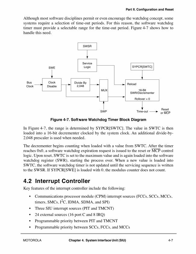
Part II. ConÞguration and Reset
Although most software disciplines permit or even encourage the watchdog concept, somesystems require a selection of time-out periods. For this reason, the software watchdogtimer must provide a selectable range for the time-out period. Figure 4-7 shows how tohandle this need.
Figure 4-7. Software Watchdog Timer Block Diagram
In Figure 4-7, the range is determined by SYPCR[SWTC]. The value in SWTC is thenloaded into a 16-bit decrementer clocked by the system clock. An additional divide-by-2,048 prescaler is used when needed.
The decrementer begins counting when loaded with a value from SWTC. After the timerreaches 0x0, a software watchdog expiration request is issued to the reset or MCP controllogic. Upon reset, SWTC is set to the maximum value and is again loaded into the softwarewatchdog register (SWR), starting the process over. When a new value is loaded intoSWTC, the software watchdog timer is not updated until the servicing sequence is writtento the SWSR. If SYPCR[SWE] is loaded with 0, the modulus counter does not count.
4.2 Interrupt ControllerKey features of the interrupt controller include the following:
¥ Communications processor module (CPM) interrupt sources (FCCs, SCCs, MCCs, timers, SMCs, I2C, IDMA, SDMA, and SPI)
¥ Three SIU interrupt sources (PIT and TMCNT)
¥ 24 external sources (16 port C and 8 IRQ)
¥ Programmable priority between PIT and TMCNT
¥ Programmable priority between SCCs, FCCs, and MCCs
DisableClock
SWR/Decrementer
Time-out
16-Bit
SYPCR[SWTC]SWE
ServiceLogic
Reload
Rollover = 0
Reset
SWSR
MUX
2,048Bus
SWP
ClockDivide By
or MCP
MOTOROLA Chapter 4. System Interface Unit (SIU) 4-7
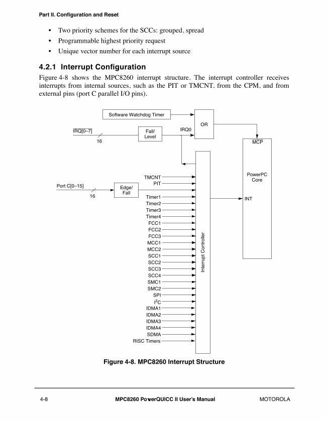
Part II. ConÞguration and Reset
¥ Two priority schemes for the SCCs: grouped, spread
¥ Programmable highest priority request
¥ Unique vector number for each interrupt source
4.2.1 Interrupt ConÞgurationFigure 4-8 shows the MPC8260 interrupt structure. The interrupt controller receivesinterrupts from internal sources, such as the PIT or TMCNT, from the CPM, and fromexternal pins (port C parallel I/O pins).
Figure 4-8. MPC8260 Interrupt Structure
MCP
IRQ[0Ð7]
INT
OR
PowerPCCore
Port C[0Ð15]
Timer1Timer2Timer3Timer4
SCC3SCC4SMC1
SPI
I2C
SMC2
Software Watchdog Timer
IRQ0
Inte
rrup
t Con
trol
ler
IDMA1IDMA2
RISC Timers
Fall/Level
SCC2SCC1
MCC1FCC3FCC2FCC1
PITTMCNT
Edge/Fall
IDMA3IDMA4SDMA
MCC2
16
16
4-8 MPC8260 PowerQUICC II UserÕs Manual MOTOROLA
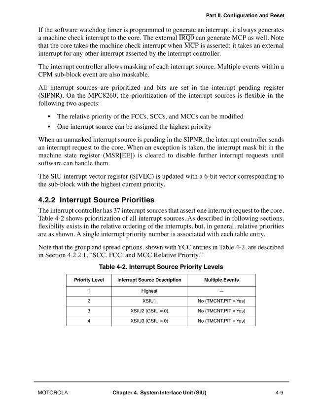
Part II. ConÞguration and Reset
If the software watchdog timer is programmed to generate an interrupt, it always generatesa machine check interrupt to the core. The external IRQ0 can generate MCP as well. Notethat the core takes the machine check interrupt when MCP is asserted; it takes an externalinterrupt for any other interrupt asserted by the interrupt controller.
The interrupt controller allows masking of each interrupt source. Multiple events within aCPM sub-block event are also maskable.
All interrupt sources are prioritized and bits are set in the interrupt pending register(SIPNR). On the MPC8260, the prioritization of the interrupt sources is ßexible in thefollowing two aspects:
¥ The relative priority of the FCCs, SCCs, and MCCs can be modiÞed
¥ One interrupt source can be assigned the highest priority
When an unmasked interrupt source is pending in the SIPNR, the interrupt controller sendsan interrupt request to the core. When an exception is taken, the interrupt mask bit in themachine state register (MSR[EE]) is cleared to disable further interrupt requests untilsoftware can handle them.
The SIU interrupt vector register (SIVEC) is updated with a 6-bit vector corresponding tothe sub-block with the highest current priority.
4.2.2 Interrupt Source PrioritiesThe interrupt controller has 37 interrupt sources that assert one interrupt request to the core.Table 4-2 shows prioritization of all interrupt sources. As described in following sections,ßexibility exists in the relative ordering of the interrupts, but, in general, relative prioritiesare as shown. A single interrupt priority number is associated with each table entry.
Note that the group and spread options, shown with YCC entries in Table 4-2, are describedin Section 4.2.2.1, ÒSCC, FCC, and MCC Relative Priority.Ó
Table 4-2. Interrupt Source Priority Levels
Priority Level Interrupt Source Description Multiple Events
1 Highest Ñ
2 XSIU1 No (TMCNT,PIT = Yes)
3 XSIU2 (GSIU = 0) No (TMCNT,PIT = Yes)
4 XSIU3 (GSIU = 0) No (TMCNT,PIT = Yes)
MOTOROLA Chapter 4. System Interface Unit (SIU) 4-9
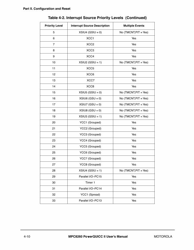
Part II. ConÞguration and Reset
5 XSIU4 (GSIU = 0) No (TMCNT,PIT = Yes)
6 XCC1 Yes
7 XCC2 Yes
8 XCC3 Yes
9 XCC4 Yes
10 XSIU2 (GSIU = 1) No (TMCNT,PIT = Yes)
11 XCC5 Yes
12 XCC6 Yes
13 XCC7 Yes
14 XCC8 Yes
15 XSIU5 (GSIU = 0) No (TMCNT,PIT = Yes)
16 XSIU6 (GSU = 0) No (TMCNT,PIT = Yes)
17 XSIU7 (GSU = 0) No (TMCNT,PIT = Yes)
18 XSIU8 (GSU = 0) No (TMCNT,PIT = Yes)
19 XSIU3 (GSIU = 1) No (TMCNT,PIT = Yes)
20 YCC1 (Grouped) Yes
21 YCC2 (Grouped) Yes
22 YCC3 (Grouped) Yes
23 YCC4 (Grouped) Yes
24 YCC5 (Grouped) Yes
25 YCC6 (Grouped) Yes
26 YCC7 (Grouped) Yes
27 YCC8 (Grouped) Yes
28 XSIU4 (GSIU = 1) No (TMCNT,PIT = Yes)
29 Parallel I/OÐPC15 Yes
30 Timer 1 Yes
31 Parallel I/OÐPC14 Yes
32 YCC1 (Spread) Yes
33 Parallel I/OÐPC13 Yes
Table 4-2. Interrupt Source Priority Levels (Continued)
Priority Level Interrupt Source Description Multiple Events
4-10 MPC8260 PowerQUICC II UserÕs Manual MOTOROLA
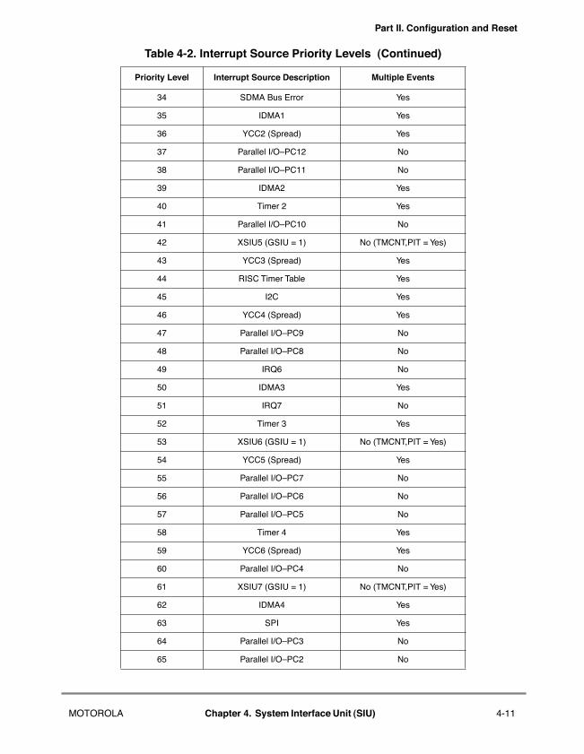
Part II. ConÞguration and Reset
34 SDMA Bus Error Yes
35 IDMA1 Yes
36 YCC2 (Spread) Yes
37 Parallel I/OÐPC12 No
38 Parallel I/OÐPC11 No
39 IDMA2 Yes
40 Timer 2 Yes
41 Parallel I/OÐPC10 No
42 XSIU5 (GSIU = 1) No (TMCNT,PIT = Yes)
43 YCC3 (Spread) Yes
44 RISC Timer Table Yes
45 I2C Yes
46 YCC4 (Spread) Yes
47 Parallel I/OÐPC9 No
48 Parallel I/OÐPC8 No
49 IRQ6 No
50 IDMA3 Yes
51 IRQ7 No
52 Timer 3 Yes
53 XSIU6 (GSIU = 1) No (TMCNT,PIT = Yes)
54 YCC5 (Spread) Yes
55 Parallel I/OÐPC7 No
56 Parallel I/OÐPC6 No
57 Parallel I/OÐPC5 No
58 Timer 4 Yes
59 YCC6 (Spread) Yes
60 Parallel I/OÐPC4 No
61 XSIU7 (GSIU = 1) No (TMCNT,PIT = Yes)
62 IDMA4 Yes
63 SPI Yes
64 Parallel I/OÐPC3 No
65 Parallel I/OÐPC2 No
Table 4-2. Interrupt Source Priority Levels (Continued)
Priority Level Interrupt Source Description Multiple Events
MOTOROLA Chapter 4. System Interface Unit (SIU) 4-11
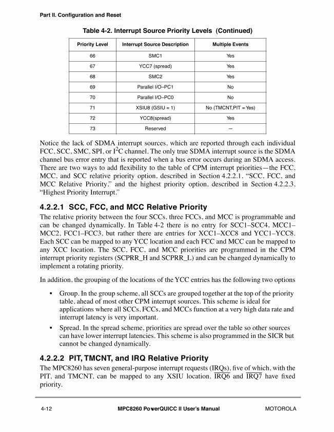
Part II. ConÞguration and Reset
Notice the lack of SDMA interrupt sources, which are reported through each individualFCC, SCC, SMC, SPI, or I2C channel. The only true SDMA interrupt source is the SDMAchannel bus error entry that is reported when a bus error occurs during an SDMA access.There are two ways to add ßexibility to the table of CPM interrupt prioritiesÑthe FCC,MCC, and SCC relative priority option, described in Section 4.2.2.1, ÒSCC, FCC, andMCC Relative Priority,Ó and the highest priority option, described in Section 4.2.2.3,ÒHighest Priority Interrupt.Ó
4.2.2.1 SCC, FCC, and MCC Relative PriorityThe relative priority between the four SCCs, three FCCs, and MCC is programmable andcan be changed dynamically. In Table 4-2 there is no entry for SCC1ÐSCC4, MCC1ÐMCC2, FCC1ÐFCC3, but rather there are entries for XCC1ÐXCC8 and YCC1ÐYCC8.Each SCC can be mapped to any YCC location and each FCC and MCC can be mapped toany XCC location. The SCC, FCC, and MCC priorities are programmed in the CPMinterrupt priority registers (SCPRR_H and SCPRR_L) and can be changed dynamically toimplement a rotating priority.
In addition, the grouping of the locations of the YCC entries has the following two options
¥ Group. In the group scheme, all SCCs are grouped together at the top of the priority table, ahead of most other CPM interrupt sources. This scheme is ideal for applications where all SCCs, FCCs, and MCCs function at a very high data rate and interrupt latency is very important.
¥ Spread. In the spread scheme, priorities are spread over the table so other sources can have lower interrupt latencies. This scheme is also programmed in the SICR but cannot be changed dynamically.
4.2.2.2 PIT, TMCNT, and IRQ Relative PriorityThe MPC8260 has seven general-purpose interrupt requests (IRQs), Þve of which, with thePIT, and TMCNT, can be mapped to any XSIU location. IRQ6 and IRQ7 have Þxedpriority.
66 SMC1 Yes
67 YCC7 (spread) Yes
68 SMC2 Yes
69 Parallel I/OÐPC1 No
70 Parallel I/OÐPC0 No
71 XSIU8 (GSIU = 1) No (TMCNT,PIT = Yes)
72 YCC8(spread) Yes
73 Reserved Ñ
Table 4-2. Interrupt Source Priority Levels (Continued)
Priority Level Interrupt Source Description Multiple Events
4-12 MPC8260 PowerQUICC II UserÕs Manual MOTOROLA
Part II. ConÞguration and Reset
4.2.2.3 Highest Priority InterruptIn addition to the FCC/MCC/SCC relative priority option, SICR[HP] can be used to specifyone interrupt source as having highest priority. This interrupt remains within the sameinterrupt level as the other interrupt controller interrupts, but is serviced before any otherinterrupt in the table.
If the highest priority feature is not used, select the interrupt request in XSIU1 to be thehighest priority interrupt; the standard interrupt priority order is used. SICR[HP] can beupdated dynamically to allow the user to change a normally low priority source into a highpriority-source for a certain period.
4.2.3 Masking Interrupt Sources By programming the SIU mask registers, SIMR_H and SIMR_L, the user can maskinterrupt requests to the core. Each SIMR bit corresponds an interrupt source. To enable aninterrupt, write a one to the corresponding SIMR bit. When a masked interrupt source hasa pending interrupt request, the corresponding SIPNR bit is set, even though the interruptis not generated to the core. The user can mask all interrupt sources to implement a pollinginterrupt servicing scheme.
When an interrupt source has multiple interrupting events, the user can individually maskthese events by programming a mask register within that block. Table 4-2 shows whichinterrupt sources have multiple interrupting events. Figure 4-9 shows an example of howthe masking occurs, using an SCC as an example.
MOTOROLA Chapter 4. System Interface Unit (SIU) 4-13
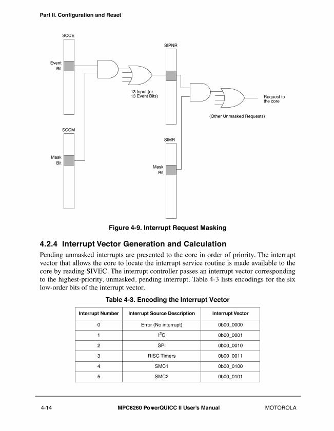
Part II. ConÞguration and Reset
Figure 4-9. Interrupt Request Masking
4.2.4 Interrupt Vector Generation and CalculationPending unmasked interrupts are presented to the core in order of priority. The interruptvector that allows the core to locate the interrupt service routine is made available to thecore by reading SIVEC. The interrupt controller passes an interrupt vector correspondingto the highest-priority, unmasked, pending interrupt. Table 4-3 lists encodings for the sixlow-order bits of the interrupt vector.
Table 4-3. Encoding the Interrupt Vector
Interrupt Number Interrupt Source Description Interrupt Vector
0 Error (No interrupt) 0b00_0000
1 I2C 0b00_0001
2 SPI 0b00_0010
3 RISC Timers 0b00_0011
4 SMC1 0b00_0100
5 SMC2 0b00_0101
SCCE
SCCM
13 Input (or
SIPNR
MaskBit
SIMR
(Other Unmasked Requests)
Request tothe core
MaskBit
EventBit
13 Event Bits)
4-14 MPC8260 PowerQUICC II UserÕs Manual MOTOROLA
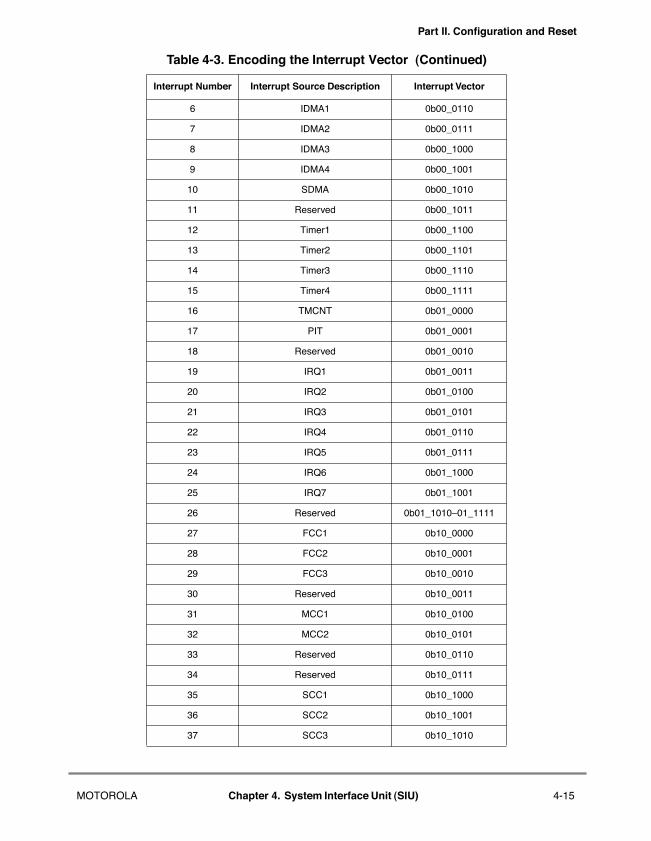
Part II. ConÞguration and Reset
6 IDMA1 0b00_0110
7 IDMA2 0b00_0111
8 IDMA3 0b00_1000
9 IDMA4 0b00_1001
10 SDMA 0b00_1010
11 Reserved 0b00_1011
12 Timer1 0b00_1100
13 Timer2 0b00_1101
14 Timer3 0b00_1110
15 Timer4 0b00_1111
16 TMCNT 0b01_0000
17 PIT 0b01_0001
18 Reserved 0b01_0010
19 IRQ1 0b01_0011
20 IRQ2 0b01_0100
21 IRQ3 0b01_0101
22 IRQ4 0b01_0110
23 IRQ5 0b01_0111
24 IRQ6 0b01_1000
25 IRQ7 0b01_1001
26 Reserved 0b01_1010Ð01_1111
27 FCC1 0b10_0000
28 FCC2 0b10_0001
29 FCC3 0b10_0010
30 Reserved 0b10_0011
31 MCC1 0b10_0100
32 MCC2 0b10_0101
33 Reserved 0b10_0110
34 Reserved 0b10_0111
35 SCC1 0b10_1000
36 SCC2 0b10_1001
37 SCC3 0b10_1010
Table 4-3. Encoding the Interrupt Vector (Continued)
Interrupt Number Interrupt Source Description Interrupt Vector
MOTOROLA Chapter 4. System Interface Unit (SIU) 4-15
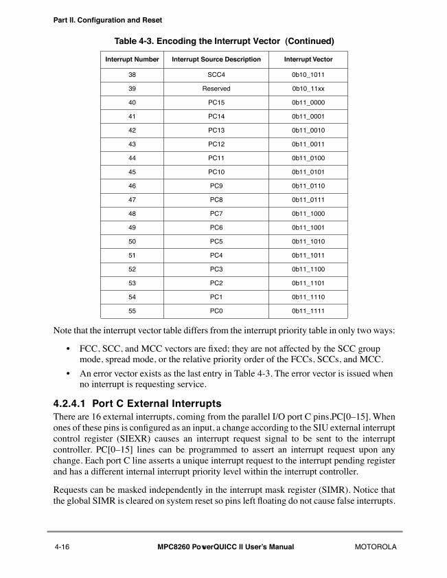
Part II. ConÞguration and Reset
Note that the interrupt vector table differs from the interrupt priority table in only two ways:
¥ FCC, SCC, and MCC vectors are Þxed; they are not affected by the SCC group mode, spread mode, or the relative priority order of the FCCs, SCCs, and MCC.
¥ An error vector exists as the last entry in Table 4-3. The error vector is issued when no interrupt is requesting service.
4.2.4.1 Port C External Interrupts There are 16 external interrupts, coming from the parallel I/O port C pins,PC[0Ð15]. Whenones of these pins is conÞgured as an input, a change according to the SIU external interruptcontrol register (SIEXR) causes an interrupt request signal to be sent to the interruptcontroller. PC[0Ð15] lines can be programmed to assert an interrupt request upon anychange. Each port C line asserts a unique interrupt request to the interrupt pending registerand has a different internal interrupt priority level within the interrupt controller.
Requests can be masked independently in the interrupt mask register (SIMR). Notice thatthe global SIMR is cleared on system reset so pins left ßoating do not cause false interrupts.
38 SCC4 0b10_1011
39 Reserved 0b10_11xx
40 PC15 0b11_0000
41 PC14 0b11_0001
42 PC13 0b11_0010
43 PC12 0b11_0011
44 PC11 0b11_0100
45 PC10 0b11_0101
46 PC9 0b11_0110
47 PC8 0b11_0111
48 PC7 0b11_1000
49 PC6 0b11_1001
50 PC5 0b11_1010
51 PC4 0b11_1011
52 PC3 0b11_1100
53 PC2 0b11_1101
54 PC1 0b11_1110
55 PC0 0b11_1111
Table 4-3. Encoding the Interrupt Vector (Continued)
Interrupt Number Interrupt Source Description Interrupt Vector
4-16 MPC8260 PowerQUICC II UserÕs Manual MOTOROLA
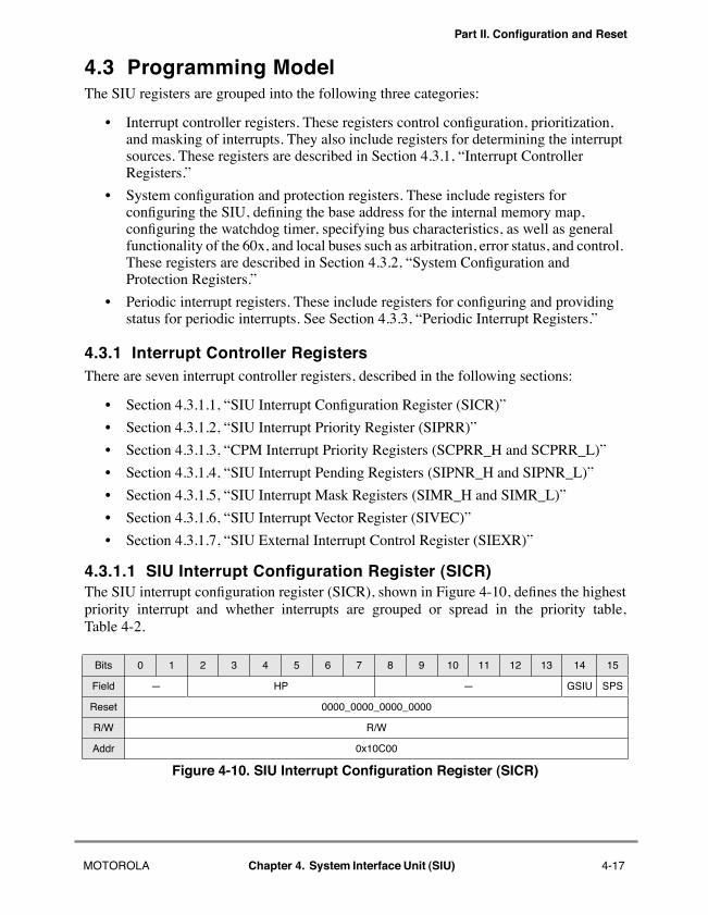
Part II. ConÞguration and Reset
4.3 Programming ModelThe SIU registers are grouped into the following three categories:
¥ Interrupt controller registers. These registers control conÞguration, prioritization, and masking of interrupts. They also include registers for determining the interrupt sources. These registers are described in Section 4.3.1, ÒInterrupt Controller Registers.Ó
¥ System conÞguration and protection registers. These include registers for conÞguring the SIU, deÞning the base address for the internal memory map, conÞguring the watchdog timer, specifying bus characteristics, as well as general functionality of the 60x, and local buses such as arbitration, error status, and control. These registers are described in Section 4.3.2, ÒSystem ConÞguration and Protection Registers.Ó
¥ Periodic interrupt registers. These include registers for conÞguring and providing status for periodic interrupts. See Section 4.3.3, ÒPeriodic Interrupt Registers.Ó
4.3.1 Interrupt Controller RegistersThere are seven interrupt controller registers, described in the following sections:
¥ Section 4.3.1.1, ÒSIU Interrupt ConÞguration Register (SICR)Ó
¥ Section 4.3.1.2, ÒSIU Interrupt Priority Register (SIPRR)Ó
¥ Section 4.3.1.3, ÒCPM Interrupt Priority Registers (SCPRR_H and SCPRR_L)Ó
¥ Section 4.3.1.4, ÒSIU Interrupt Pending Registers (SIPNR_H and SIPNR_L)Ó
¥ Section 4.3.1.5, ÒSIU Interrupt Mask Registers (SIMR_H and SIMR_L)Ó
¥ Section 4.3.1.6, ÒSIU Interrupt Vector Register (SIVEC)Ó
¥ Section 4.3.1.7, ÒSIU External Interrupt Control Register (SIEXR)Ó
4.3.1.1 SIU Interrupt ConÞguration Register (SICR)The SIU interrupt conÞguration register (SICR), shown in Figure 4-10, deÞnes the highestpriority interrupt and whether interrupts are grouped or spread in the priority table,Table 4-2.
Bits 0 1 2 3 4 5 6 7 8 9 10 11 12 13 14 15
Field Ñ HP Ñ GSIU SPS
Reset 0000_0000_0000_0000
R/W R/W
Addr 0x10C00
Figure 4-10. SIU Interrupt Configuration Register (SICR)
MOTOROLA Chapter 4. System Interface Unit (SIU) 4-17
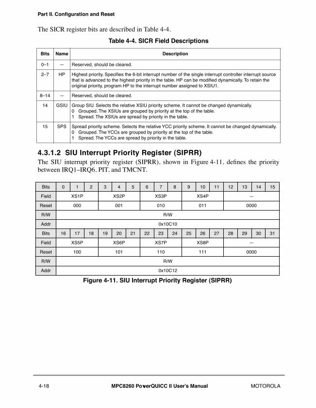
Part II. ConÞguration and Reset
The SICR register bits are described in Table 4-4.
4.3.1.2 SIU Interrupt Priority Register (SIPRR)The SIU interrupt priority register (SIPRR), shown in Figure 4-11, deÞnes the prioritybetween IRQ1ÐIRQ6, PIT, and TMCNT.
Table 4-4. SICR Field Descriptions
Bits Name Description
0Ð1 Ñ Reserved, should be cleared.
2Ð7 HP Highest priority. SpeciÞes the 6-bit interrupt number of the single interrupt controller interrupt source that is advanced to the highest priority in the table. HP can be modiÞed dynamically. To retain the original priority, program HP to the interrupt number assigned to XSIU1.
8Ð14 Ñ Reserved, should be cleared.
14 GSIU Group SIU. Selects the relative XSIU priority scheme. It cannot be changed dynamically.0 Grouped. The XSIUs are grouped by priority at the top of the table.1 Spread. The XSIUs are spread by priority in the table.
15 SPS Spread priority scheme. Selects the relative YCC priority scheme. It cannot be changed dynamically.0 Grouped. The YCCs are grouped by priority at the top of the table.1 Spread. The YCCs are spread by priority in the table.
Bits 0 1 2 3 4 5 6 7 8 9 10 11 12 13 14 15
Field XS1P XS2P XS3P XS4P Ñ
Reset 000 001 010 011 0000
R/W R/W
Addr 0x10C10
Bits 16 17 18 19 20 21 22 23 24 25 26 27 28 29 30 31
Field XS5P XS6P XS7P XS8P Ñ
Reset 100 101 110 111 0000
R/W R/W
Addr 0x10C12
Figure 4-11. SIU Interrupt Priority Register (SIPRR)
4-18 MPC8260 PowerQUICC II UserÕs Manual MOTOROLA
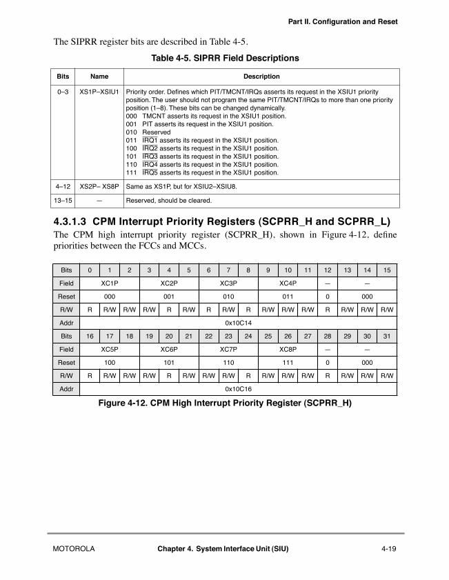
Part II. ConÞguration and Reset
The SIPRR register bits are described in Table 4-5.
4.3.1.3 CPM Interrupt Priority Registers (SCPRR_H and SCPRR_L)The CPM high interrupt priority register (SCPRR_H), shown in Figure 4-12, deÞnepriorities between the FCCs and MCCs.
Table 4-5. SIPRR Field Descriptions
Bits Name Description
0Ð3 XS1PÐXSIU1 Priority order. DeÞnes which PIT/TMCNT/IRQs asserts its request in the XSIU1 priority position. The user should not program the same PIT/TMCNT/IRQs to more than one priority position (1Ð8). These bits can be changed dynamically.000 TMCNT asserts its request in the XSIU1 position.001 PIT asserts its request in the XSIU1 position.010 Reserved011 IRQ1 asserts its request in the XSIU1 position.100 IRQ2 asserts its request in the XSIU1 position.101 IRQ3 asserts its request in the XSIU1 position.110 IRQ4 asserts its request in the XSIU1 position.111 IRQ5 asserts its request in the XSIU1 position.
4Ð12 XS2PÐ XS8P Same as XS1P, but for XSIU2ÐXSIU8.
13Ð15 Ñ Reserved, should be cleared.
Bits 0 1 2 3 4 5 6 7 8 9 10 11 12 13 14 15
Field XC1P XC2P XC3P XC4P Ñ Ñ
Reset 000 001 010 011 0 000
R/W R R/W R/W R/W R R/W R R/W R R/W R/W R/W R R/W R/W R/W
Addr 0x10C14
Bits 16 17 18 19 20 21 22 23 24 25 26 27 28 29 30 31
Field XC5P XC6P XC7P XC8P Ñ Ñ
Reset 100 101 110 111 0 000
R/W R R/W R/W R/W R R/W R/W R/W R R/W R/W R/W R R/W R/W R/W
Addr 0x10C16
Figure 4-12. CPM High Interrupt Priority Register (SCPRR_H)
MOTOROLA Chapter 4. System Interface Unit (SIU) 4-19
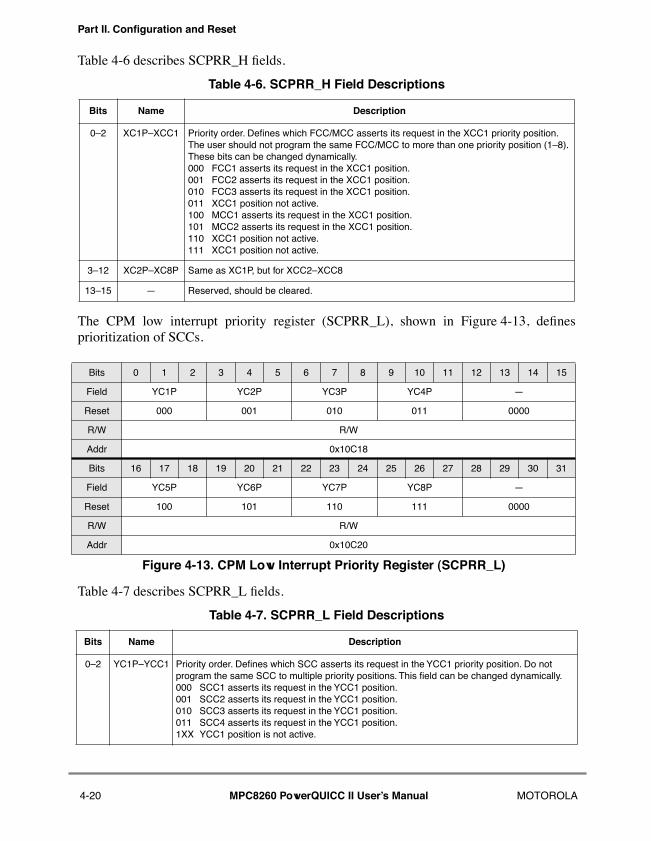
Part II. ConÞguration and Reset
Table 4-6 describes SCPRR_H Þelds.
The CPM low interrupt priority register (SCPRR_L), shown in Figure 4-13, deÞnesprioritization of SCCs.
Table 4-7 describes SCPRR_L Þelds.
Table 4-6. SCPRR_H Field Descriptions
Bits Name Description
0Ð2 XC1PÐXCC1 Priority order. DeÞnes which FCC/MCC asserts its request in the XCC1 priority position. The user should not program the same FCC/MCC to more than one priority position (1Ð8). These bits can be changed dynamically.000 FCC1 asserts its request in the XCC1 position.001 FCC2 asserts its request in the XCC1 position.010 FCC3 asserts its request in the XCC1 position.011 XCC1 position not active.100 MCC1 asserts its request in the XCC1 position.101 MCC2 asserts its request in the XCC1 position.110 XCC1 position not active.111 XCC1 position not active.
3Ð12 XC2PÐXC8P Same as XC1P, but for XCC2ÐXCC8
13Ð15 Ñ Reserved, should be cleared.
Bits 0 1 2 3 4 5 6 7 8 9 10 11 12 13 14 15
Field YC1P YC2P YC3P YC4P Ñ
Reset 000 001 010 011 0000
R/W R/W
Addr 0x10C18
Bits 16 17 18 19 20 21 22 23 24 25 26 27 28 29 30 31
Field YC5P YC6P YC7P YC8P Ñ
Reset 100 101 110 111 0000
R/W R/W
Addr 0x10C20
Figure 4-13. CPM Low Interrupt Priority Register (SCPRR_L)
Table 4-7. SCPRR_L Field Descriptions
Bits Name Description
0Ð2 YC1PÐYCC1 Priority order. DeÞnes which SCC asserts its request in the YCC1 priority position. Do not program the same SCC to multiple priority positions. This Þeld can be changed dynamically.000 SCC1 asserts its request in the YCC1 position.001 SCC2 asserts its request in the YCC1 position.010 SCC3 asserts its request in the YCC1 position.011 SCC4 asserts its request in the YCC1 position.1XX YCC1 position is not active.
4-20 MPC8260 PowerQUICC II UserÕs Manual MOTOROLA
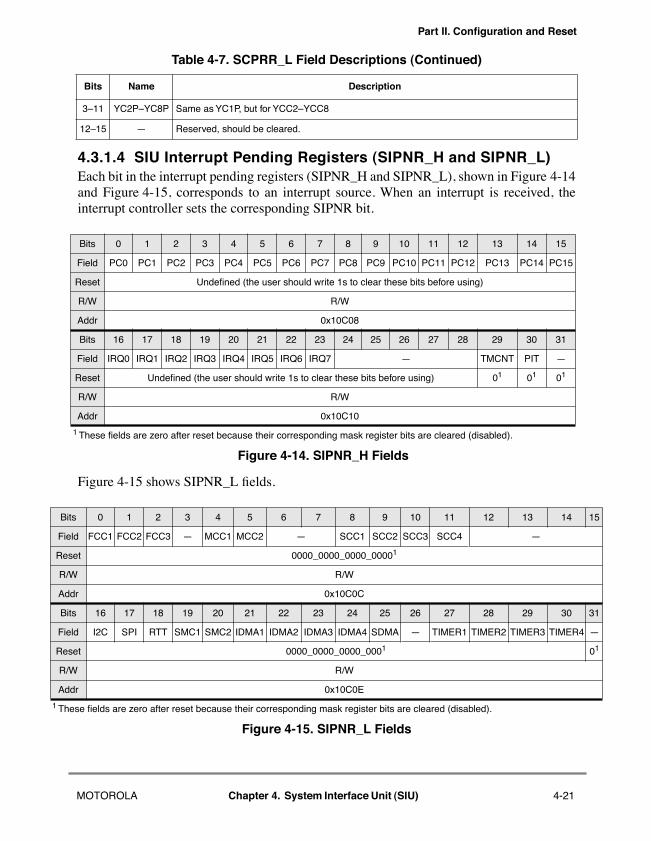
Part II. ConÞguration and Reset
Bi 15
Fie
Re
R/
Ad
Bi 31
Fie Ñ
Re 01
R/
Ad
1 Th
4.3.1.4 SIU Interrupt Pending Registers (SIPNR_H and SIPNR_L) Each bit in the interrupt pending registers (SIPNR_H and SIPNR_L), shown in Figure 4-14and Figure 4-15, corresponds to an interrupt source. When an interrupt is received, theinterrupt controller sets the corresponding SIPNR bit.
Figure 4-15 shows SIPNR_L Þelds.
3Ð11 YC2PÐYC8P Same as YC1P, but for YCC2ÐYCC8
12Ð15 Ñ Reserved, should be cleared.
Bits 0 1 2 3 4 5 6 7 8 9 10 11 12 13 14 15
Field PC0 PC1 PC2 PC3 PC4 PC5 PC6 PC7 PC8 PC9 PC10 PC11 PC12 PC13 PC14 PC15
Reset UndeÞned (the user should write 1s to clear these bits before using)
R/W R/W
Addr 0x10C08
Bits 16 17 18 19 20 21 22 23 24 25 26 27 28 29 30 31
Field IRQ0 IRQ1 IRQ2 IRQ3 IRQ4 IRQ5 IRQ6 IRQ7 Ñ TMCNT PIT Ñ
Reset UndeÞned (the user should write 1s to clear these bits before using) 01 01 01
R/W R/W
Addr 0x10C10
1 These Þelds are zero after reset because their corresponding mask register bits are cleared (disabled).
Figure 4-14. SIPNR_H Fields
ts 0 1 2 3 4 5 6 7 8 9 10 11 12 13 14
ld FCC1 FCC2 FCC3 Ñ MCC1 MCC2 Ñ SCC1 SCC2 SCC3 SCC4 Ñ
set 0000_0000_0000_00001
W R/W
dr 0x10C0C
ts 16 17 18 19 20 21 22 23 24 25 26 27 28 29 30
ld I2C SPI RTT SMC1 SMC2 IDMA1 IDMA2 IDMA3 IDMA4 SDMA Ñ TIMER1 TIMER2 TIMER3 TIMER4
set 0000_0000_0000_0001
W R/W
dr 0x10C0E
ese Þelds are zero after reset because their corresponding mask register bits are cleared (disabled).
Figure 4-15. SIPNR_L Fields
Table 4-7. SCPRR_L Field Descriptions (Continued)
Bits Name Description
MOTOROLA Chapter 4. System Interface Unit (SIU) 4-21
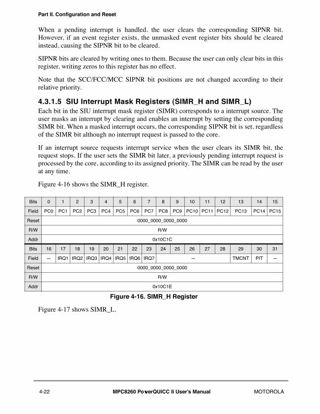
Part II. ConÞguration and Reset
Bi
Fie
Res
R/W
Ad
Bi
Fie
Res
R/W
Ad
When a pending interrupt is handled, the user clears the corresponding SIPNR bit.However, if an event register exists, the unmasked event register bits should be clearedinstead, causing the SIPNR bit to be cleared.
SIPNR bits are cleared by writing ones to them. Because the user can only clear bits in thisregister, writing zeros to this register has no effect.
Note that the SCC/FCC/MCC SIPNR bit positions are not changed according to theirrelative priority.
4.3.1.5 SIU Interrupt Mask Registers (SIMR_H and SIMR_L) Each bit in the SIU interrupt mask register (SIMR) corresponds to a interrupt source. Theuser masks an interrupt by clearing and enables an interrupt by setting the correspondingSIMR bit. When a masked interrupt occurs, the corresponding SIPNR bit is set, regardlessof the SIMR bit although no interrupt request is passed to the core.
If an interrupt source requests interrupt service when the user clears its SIMR bit, therequest stops. If the user sets the SIMR bit later, a previously pending interrupt request isprocessed by the core, according to its assigned priority. The SIMR can be read by the userat any time.
Figure 4-16 shows the SIMR_H register.
Figure 4-17 shows SIMR_L.
ts 0 1 2 3 4 5 6 7 8 9 10 11 12 13 14 15
ld PC0 PC1 PC2 PC3 PC4 PC5 PC6 PC7 PC8 PC9 PC10 PC11 PC12 PC13 PC14 PC15
et 0000_0000_0000_0000
R/W
dr 0x10C1C
ts 16 17 18 19 20 21 22 23 24 25 26 27 28 29 30 31
ld Ñ IRQ1 IRQ2 IRQ3 IRQ4 IRQ5 IRQ6 IRQ7 Ñ TMCNT PIT Ñ
et 0000_0000_0000_0000
R/W
dr 0x10C1E
Figure 4-16. SIMR_H Register
4-22 MPC8260 PowerQUICC II UserÕs Manual MOTOROLA
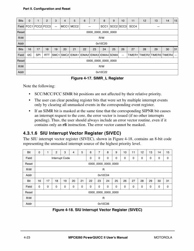
Part II. ConÞguration and Reset
B 5
Fie
Re
R/
Ad
B 1
Fie
Re
R/
Ad
Note the following:
¥ SCC/MCC/FCC SIMR bit positions are not affected by their relative priority.
¥ The user can clear pending register bits that were set by multiple interrupt events only by clearing all unmasked events in the corresponding event register.
¥ If an SIMR bit is masked at the same time that the corresponding SIPNR bit causes an interrupt request to the core, the error vector is issued (if no other interrupts pending). Thus, the user should always include an error vector routine, even if it contains only an rÞ instruction. The error vector cannot be masked.
4.3.1.6 SIU Interrupt Vector Register (SIVEC)The SIU interrupt vector register (SIVEC), shown in Figure 4-18, contains an 8-bit coderepresenting the unmasked interrupt source of the highest priority level.
its 0 1 2 3 4 5 6 7 8 9 10 11 12 13 14 1
ld FCC1 FCC2 FCC3 Ñ MCC1 MCC2 Ñ SCC1 SCC2 SCC3 SCC4 Ñ
set 0000_0000_0000_0000
W R/W
dr 0x10C20
its 16 17 18 19 20 21 22 23 24 25 26 27 28 29 30 3
ld I2C SPI RTT SMC1 SMC2 IDMA1 IDMA2 IDMA3 IDMA4 SDMA Ñ TIMER1 TIMER2 TIMER3 TIMER4 Ñ
set 0000_0000_0000_0000
W R/W
dr 0x10C22
Figure 4-17. SIMR_L Register
Bit 0 1 2 3 4 5 6 7 8 9 10 11 12 13 14 15
Field Interrupt Code 0 0 0 0 0 0 0 0 0 0
Reset 0000_0000_0000_0000
R/W R
Addr 0x10C04
Bit 16 17 18 19 20 21 22 23 24 25 26 27 28 29 30 31
Field 0 0 0 0 0 0 0 0 0 0 0 0 0 0 0 0
Reset 0000_0000_0000_0000
R/W R
Addr 0x10C06
Figure 4-18. SIU Interrupt Vector Register (SIVEC)
4-23 MPC8260 PowerQUICC II UserÕs Manual MOTOROLA
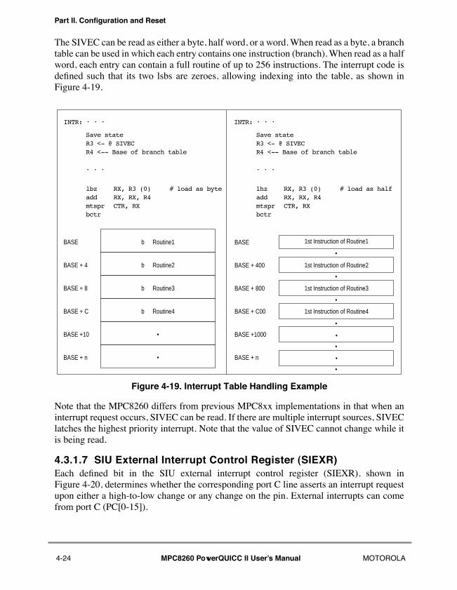
Part II. ConÞguration and Reset
The SIVEC can be read as either a byte, half word, or a word. When read as a byte, a branchtable can be used in which each entry contains one instruction (branch). When read as a halfword, each entry can contain a full routine of up to 256 instructions. The interrupt code isdeÞned such that its two lsbs are zeroes, allowing indexing into the table, as shown inFigure 4-19.
Figure 4-19. Interrupt Table Handling Example
Note that the MPC8260 differs from previous MPC8xx implementations in that when aninterrupt request occurs, SIVEC can be read. If there are multiple interrupt sources, SIVEClatches the highest priority interrupt. Note that the value of SIVEC cannot change while itis being read.
4.3.1.7 SIU External Interrupt Control Register (SIEXR)Each deÞned bit in the SIU external interrupt control register (SIEXR), shown inFigure 4-20, determines whether the corresponding port C line asserts an interrupt requestupon either a high-to-low change or any change on the pin. External interrupts can comefrom port C (PC[0-15]).
BASE b Routine1
b Routine2
b Routine3
b Routine4
•
•BASE + n
BASE + 4
BASE + 8
BASE + C
BASE +10
BASE 1st Instruction of Routine1
1st Instruction of Routine2
1st Instruction of Routine3
1st Instruction of Routine4
•
•BASE + n
BASE + 400
BASE + 800
BASE + C00
BASE +1000
•
•
•
•
•
•
INTR: ¥ ¥ ¥
Save stateR3 <- @ SIVECR4 <-- Base of branch table
¥ ¥ ¥
lbzaddmtsprbctr
RX, R3 (0) # load as byteRX, RX, R4CTR, RX
INTR: ¥ ¥ ¥
Save stateR3 <- @ SIVECR4 <-- Base of branch table
¥ ¥ ¥
lhzaddmtsprbctr
RX, R3 (0) # load as halfRX, RX, R4CTR, RX
4-24 MPC8260 PowerQUICC II UserÕs Manual MOTOROLA
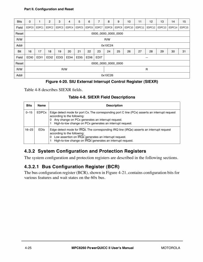
Part II. ConÞguration and Reset
Bits 5
Field PC15
Rese
R/W
Add
Bit 1
Field
Rese
R/W
Add
Table 4-8 describes SIEXR Þelds.
4.3.2 System ConÞguration and Protection Registers
The system conÞguration and protection registers are described in the following sections.
4.3.2.1 Bus ConÞguration Register (BCR)
The bus conÞguration register (BCR), shown in Figure 4-21, contains conÞguration bits forvarious features and wait states on the 60x bus.
0 1 2 3 4 5 6 7 8 9 10 11 12 13 14 1
EDPC0 EDPC1 EDPC2 EDPC3 EDPC4 EDPC5 EDPC6 EDPC7 EDPC8 EDPC9 EDPC10 EDPC11 EDPC12 EDPC13 EDPC14 ED
t 0000_0000_0000_0000
R/W
r 0x10C24
16 17 18 19 20 21 22 23 24 25 26 27 28 29 30 3
EDI0 EDI1 EDI2 EDI3 EDI4 EDI5 EDI6 EDI7 Ñ
t 0000_0000_0000_0000
R/W R
r 0x10C26
Figure 4-20. SIU External Interrupt Control Register (SIEXR)
Table 4-8. SIEXR Field Descriptions
Bits Name Description
0Ð15 EDPCx Edge detect mode for port Cx. The corresponding port C line (PCx) asserts an interrupt request according to the following:0 Any change on PCx generates an interrupt request.1 High-to-low change on PCx generates an interrupt request.
16Ð23 EDIx Edge detect mode for IRQ
x
. The corresponding IRQ line (IRQx) asserts an interrupt request according to the following:0 Low assertion on IRQ
x
generates an interrupt request.1 High-to-low change on IRQ
x
generates an interrupt request.
4-25 MPC8260 PowerQUICC II UserÕs Manual MOTOROLA
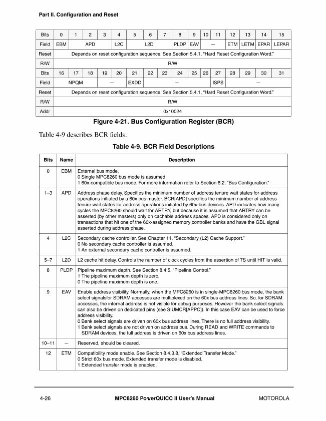
Part II. ConÞguration and Reset
Table 4-9 describes BCR Þelds.
Bits 0 1 2 3 4 5 6 7 8 9 10 11 12 13 14 15
Field EBM APD L2C L2D PLDP EAV Ñ ETM LETM EPAR LEPAR
Reset Depends on reset conÞguration sequence. See Section 5.4.1, ÒHard Reset ConÞguration Word.Ó
R/W R/W
Bits 16 17 18 19 20 21 22 23 24 25 26 27 28 29 30 31
Field NPQM Ñ EXDD Ñ ISPS Ñ
Reset Depends on reset conÞguration sequence. See Section 5.4.1, ÒHard Reset ConÞguration Word.Ó
R/W R/W
Addr 0x10024
Figure 4-21. Bus Configuration Register (BCR)
Table 4-9. BCR Field Descriptions
Bits Name Description
0 EBM External bus mode. 0 Single MPC8260 bus mode is assumed1 60x-compatible bus mode. For more information refer to Section 8.2, ÒBus ConÞguration.Ó
1Ð3 APD Address phase delay. SpeciÞes the minimum number of address tenure wait states for address operations initiated by a 60x bus master. BCR[APD] speciÞes the minimum number of address tenure wait states for address operations initiated by 60x-bus devices. APD indicates how many cycles the MPC8260 should wait for ARTRY, but because it is assumed that ARTRY can be asserted (by other masters) only on cachable address spaces, APD is considered only on transactions that hit one of the 60x-assigned memory controller banks and have the GBL signal asserted during address phase.
4 L2C Secondary cache controller. See Chapter 11, ÒSecondary (L2) Cache Support.Ó0 No secondary cache controller is assumed. 1 An external secondary cache controller is assumed.
5Ð7 L2D L2 cache hit delay. Controls the number of clock cycles from the assertion of TS until HIT is valid.
8 PLDP Pipeline maximum depth. See Section 8.4.5, ÒPipeline Control.Ó1 The pipeline maximum depth is zero. 0 The pipeline maximum depth is one.
9 EAV Enable address visibility. Normally, when the MPC8260 is in single-MPC8260 bus mode, the bank select signalsfor SDRAM accesses are multiplexed on the 60x bus address lines. So, for SDRAM accesses, the internal address is not visible for debug purposes. However the bank select signals can also be driven on dedicated pins (see SIUMCR[APPC]). In this case EAV can be used to force address visibility.0 Bank select signals are driven on 60x bus address lines. There is no full address visibility.1 Bank select signals are not driven on address bus. During READ and WRITE commands to
SDRAM devices, the full address is driven on 60x bus address lines.
10Ð11 Ñ Reserved, should be cleared.
12 ETM Compatibility mode enable. See Section 8.4.3.8, ÒExtended Transfer Mode.Ó0 Strict 60x bus mode. Extended transfer mode is disabled. 1 Extended transfer mode is enabled.
4-26 MPC8260 PowerQUICC II UserÕs Manual MOTOROLA
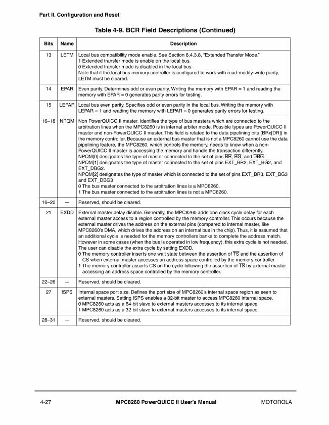
Part II. ConÞguration and Reset
13 LETM Local bus compatibility mode enable. See Section 8.4.3.8, ÒExtended Transfer Mode.Ó 1 Extended transfer mode is enable on the local bus. 0 Extended transfer mode is disabled in the local bus. Note that if the local bus memory controller is conÞgured to work with read-modify-write parity, LETM must be cleared.
14 EPAR Even parity. Determines odd or even parity, Writing the memory with EPAR = 1 and reading the memory with EPAR = 0 generates parity errors for testing.
15 LEPAR Local bus even parity. SpeciÞes odd or even parity in the local bus. Writing the memory with LEPAR = 1 and reading the memory with LEPAR = 0 generates parity errors for testing.
16Ð18 NPQM Non PowerQUICC II master. IdentiÞes the type of bus masters which are connected to the arbitration lines when the MPC8260 is in internal arbiter mode. Possible types are PowerQUICC II master and non-PowerQUICC II master. This Þeld is related to the data pipelining bits (BRx[DR]) in the memory controller. Because an external bus master that is not a MPC8260 cannot use the data pipelining feature, the MPC8260, which controls the memory, needs to know when a non-PowerQUICC II master is accessing the memory and handle the transaction differently.NPQM[0] designates the type of master connected to the set of pins BR, BG, and DBG. NPQM[1] designates the type of master connected to the set of pins EXT_BR2, EXT_BG2, and EXT_DBG2. NPQM[2] designates the type of master which is connected to the set of pins EXT_BR3, EXT_BG3 and EXT_DBG30 The bus master connected to the arbitration lines is a MPC8260.1 The bus master connected to the arbitration lines is not a MPC8260.
16Ð20 Ñ Reserved, should be cleared.
21 EXDD External master delay disable. Generally, the MPC8260 adds one clock cycle delay for each external master access to a region controlled by the memory controller. This occurs because the external master drives the address on the external pins (compared to internal master, like MPC8260Õs DMA, which drives the address on an internal bus in the chip). Thus, it is assumed that an additional cycle is needed for the memory controllers banks to complete the address match. However in some cases (when the bus is operated in low frequency), this extra cycle is not needed. The user can disable the extra cycle by setting EXDD.0 The memory controller inserts one wait state between the assertion of TS and the assertion of
CS when external master accesses an address space controlled by the memory controller.1 The memory controller asserts CS on the cycle following the assertion of TS by external master
accessing an address space controlled by the memory controller.
22Ð26 Ñ Reserved, should be cleared.
27 ISPS Internal space port size. DeÞnes the port size of MPC8260Õs internal space region as seen to external masters. Setting ISPS enables a 32-bit master to access MPC8260 internal space.0 MPC8260 acts as a 64-bit slave to external masters accesses to its internal space.1 MPC8260 acts as a 32-bit slave to external masters accesses to its internal space.
28Ð31 Ñ Reserved, should be cleared.
Table 4-9. BCR Field Descriptions (Continued)
Bits Name Description
4-27 MPC8260 PowerQUICC II UserÕs Manual MOTOROLA
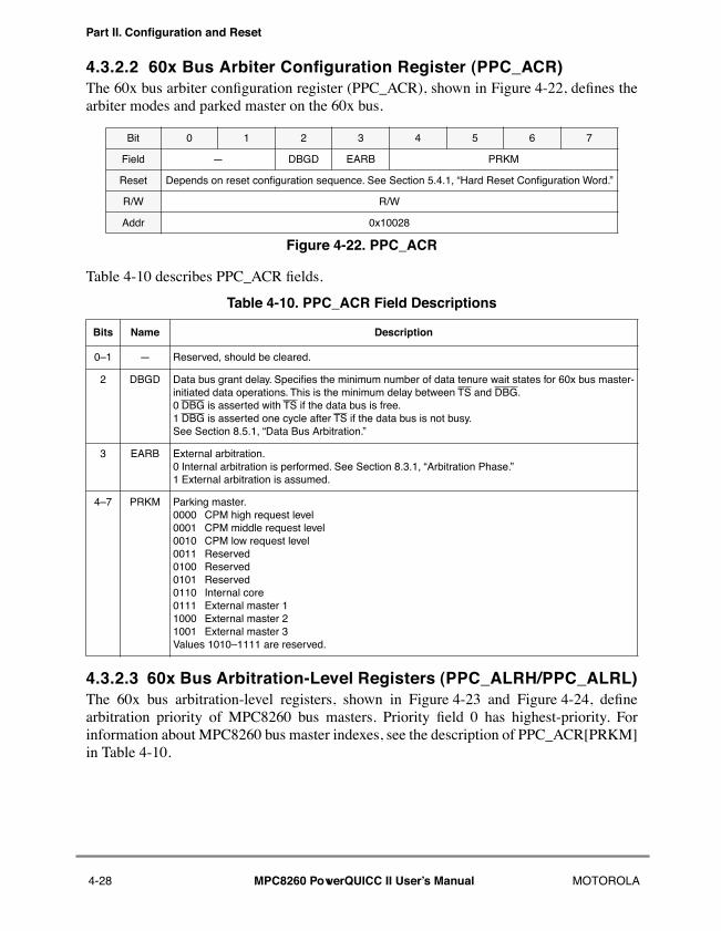
Part II. ConÞguration and Reset
4.3.2.2 60x Bus Arbiter ConÞguration Register (PPC_ACR)The 60x bus arbiter conÞguration register (PPC_ACR), shown in Figure 4-22, deÞnes thearbiter modes and parked master on the 60x bus.
Table 4-10 describes PPC_ACR Þelds.
4.3.2.3 60x Bus Arbitration-Level Registers (PPC_ALRH/PPC_ALRL)The 60x bus arbitration-level registers, shown in Figure 4-23 and Figure 4-24, deÞnearbitration priority of MPC8260 bus masters. Priority Þeld 0 has highest-priority. Forinformation about MPC8260 bus master indexes, see the description of PPC_ACR[PRKM]in Table 4-10.
Bit 0 1 2 3 4 5 6 7
Field Ñ DBGD EARB PRKM
Reset Depends on reset conÞguration sequence. See Section 5.4.1, ÒHard Reset ConÞguration Word.Ó
R/W R/W
Addr 0x10028
Figure 4-22. PPC_ACR
Table 4-10. PPC_ACR Field Descriptions
Bits Name Description
0Ð1 Ñ Reserved, should be cleared.
2 DBGD Data bus grant delay. SpeciÞes the minimum number of data tenure wait states for 60x bus master-initiated data operations. This is the minimum delay between TS and DBG. 0 DBG is asserted with TS if the data bus is free. 1 DBG is asserted one cycle after TS if the data bus is not busy. See Section 8.5.1, ÒData Bus Arbitration.Ó
3 EARB External arbitration. 0 Internal arbitration is performed. See Section 8.3.1, ÒArbitration Phase.Ó1 External arbitration is assumed.
4Ð7 PRKM Parking master. 0000 CPM high request level0001 CPM middle request level0010 CPM low request level0011 Reserved0100 Reserved0101 Reserved0110 Internal core0111 External master 11000 External master 21001 External master 3Values 1010Ð1111 are reserved.
4-28 MPC8260 PowerQUICC II UserÕs Manual MOTOROLA
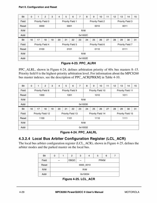
Part II. ConÞguration and Reset
PPC_ALRL, shown in Figure 4-24, deÞnes arbitration priority of 60x bus masters 8Ð15.Priority Þeld 0 is the highest-priority arbitration level. For information about the MPC8260bus master indexes, see the description of PPC_ACR[PRKM] in Table 4-10.
4.3.2.4 Local Bus Arbiter ConÞguration Register (LCL_ACR)The local bus arbiter conÞguration register (LCL_ACR), shown in Figure 4-25, deÞnes thearbiter modes and the parked master on the local bus.
Bit 0 1 2 3 4 5 6 7 8 9 10 11 12 13 14 15
Field Priority Field 0 Priority Field 1 Priority Field 2 Priority Field 3
Reset 0000 0001 0010 0011
R/W R/W
Addr 0x1002C
Bit 16 17 18 19 20 21 22 23 24 25 26 27 28 29 30 31
Field Priority Field 4 Priority Field 5 Priority Field 6 Priority Field 7
Reset 0100 0101 0110 0111
R/W R/W
Addr 0x1002E
Figure 4-23. PPC_ALRH
Bit 0 1 2 3 4 5 6 7 8 9 10 11 12 13 14 15
Field Priority Field 8 Priority Field 9 Priority Field 10 Priority Field 11
Reset 1000 1001 1010 1011
R/W R/W
Addr 0x10030
Bit 16 17 18 19 20 21 22 23 24 25 26 27 28 29 30 31
Field Priority Field 12 Priority Field 13 Priority Field 14 Priority Field 15
Reset 1100 1101 1110 1111
R/W R/W
Addr 0x10032
Figure 4-24. PPC_AALRL
Bit 0 1 2 3 4 5 6 7
Field Ñ DBGD Ñ PRKM
Reset 0000_0010
R/W R/W
Addr 0x10034
Figure 4-25. LCL_ACR
4-29 MPC8260 PowerQUICC II UserÕs Manual MOTOROLA
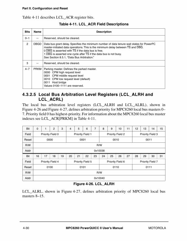
Part II. ConÞguration and Reset
Table 4-11 describes LCL_ACR register bits.
4.3.2.5 Local Bus Arbitration Level Registers (LCL_ALRH and LCL_ACRL)
The local bus arbitration level registers (LCL_ALRH and LCL_ALRL), shown inFigure 4-26 and Figure 4-27, deÞnes arbitration priority for MPC8260 local bus masters 0Ð7. Priority Þeld 0 has highest-priority. For information about the MPC8260 local bus masterindexes see LCL_ACR[PRKM] in Table 4-11.
LCL_ALRL, shown in Figure 4-27, deÞnes arbitration priority of MPC8260 local busmasters 8Ð15.
Table 4-11. LCL_ACR Field Descriptions
Bits Name Description
0Ð1 Ñ Reserved, should be cleared.
2 DBGD Data bus grant delay. SpeciÞes the minimum number of data tenure wait states for PowerPC master-initiated data operations. This is the minimum delay between TS and DBG. 0 DBG is asserted with TS if the data bus is free. 1 DBG is asserted one cycle after TS if the data bus is not busy. See Section 8.5.1, ÒData Bus Arbitration.Ó
3 Ñ Reserved, should be cleared.
4Ð7 PRKM Parking master. DeÞnes the parked master. 0000 CPM high request level0001 CPM middle request level0010 CPM low request level (default)0011 Host bridgeValues 0100Ð1111 are reserved.
Bit 0 1 2 3 4 5 6 7 8 9 10 11 12 13 14 15
Field Priority Field 0 Priority Field 1 Priority Field 2 Priority Field 3
Reset 0000 0001 0010 0011
R/W R/W
Addr 0x10038
Bit 16 17 18 19 20 21 22 23 24 25 26 27 28 29 30 31
Field Priority Field 4 Priority Field 5 Priority Field 6 Priority Field 7
Reset 0100 0101 0110 0111
R/W R/W
Addr 0x10040
Figure 4-26. LCL_ALRH
4-30 MPC8260 PowerQUICC II UserÕs Manual MOTOROLA
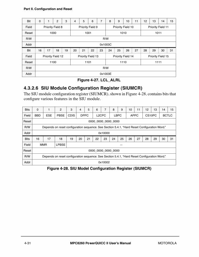
Part II. ConÞguration and Reset
4.3.2.6 SIU Module ConÞguration Register (SIUMCR)The SIU module conÞguration register (SIUMCR), shown in Figure 4-28, contains bits thatconÞgure various features in the SIU module.
Bit 0 1 2 3 4 5 6 7 8 9 10 11 12 13 14 15
Field Priority Field 8 Priority Field 9 Priority Field 10 Priority Field 11
Reset 1000 1001 1010 1011
R/W R/W
Addr 0x1003C
Bit 16 17 18 19 20 21 22 23 24 25 26 27 28 29 30 31
Field Priority Field 12 Priority Field 13 Priority Field 14 Priority Field 15
Reset 1100 1101 1110 1111
R/W R/W
Addr 0x1003E
Figure 4-27. LCL_ALRL
Bits 0 1 2 3 4 5 6 7 8 9 10 11 12 13 14 15
Field BBD ESE PBSE CDIS DPPC L2CPC LBPC APPC CS10PC BCTLC
Reset 0000_0000_0000_0000
R/W Depends on reset conÞguration sequence. See Section 5.4.1, ÒHard Reset ConÞguration Word.Ó
Addr 0x10000
Bits 16 17 18 19 20 21 22 23 24 25 26 27 28 29 30 31
Field MMR LPBSE Ñ
Reset 0000_0000_0000_0000
R/W Depends on reset conÞguration sequence. See Section 5.4.1, ÒHard Reset ConÞguration Word.Ó
Addr 0x10002
Figure 4-28. SIU Model Configuration Register (SIUMCR)
4-31 MPC8260 PowerQUICC II UserÕs Manual MOTOROLA
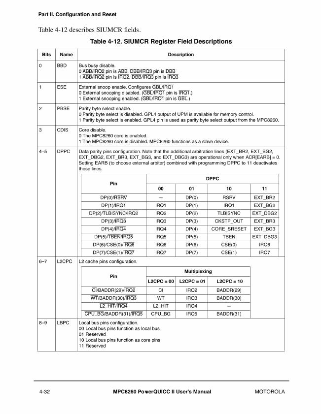
Part II. ConÞguration and Reset
Table 4-12 describes SIUMCR Þelds.
Table 4-12. SIUMCR Register Field Descriptions
Bits Name Description
0 BBD Bus busy disable. 0 ABB/IRQ2 pin is ABB, DBB/IRQ3 pin is DBB1 ABB/IRQ2 pin is IRQ2, DBB/IRQ3 pin is IRQ3
1 ESE External snoop enable. ConÞgures GBL/IRQ10 External snooping disabled. (GBL/IRQ1 pin is IRQ1.) 1 External snooping enabled. (GBL/IRQ1 pin is GBL.)
2 PBSE Parity byte select enable. 0 Parity byte select is disabled. GPL4 output of UPM is available for memory control.1 Parity byte select is enabled. GPL4 pin is used as parity byte select output from the MPC8260.
3 CDIS Core disable.0 The MPC8260 core is enabled.1 The MPC8260 core is disabled. MPC8260 functions as a slave device.
4Ð5 DPPC Data parity pins conÞguration. Note that the additional arbitration lines (EXT_BR2, EXT_BG2, EXT_DBG2, EXT_BR3, EXT_BG3, and EXT_DBG3) are operational only when ACR[EARB] = 0. Setting EARB (to choose external arbiter) combined with programming DPPC to 11 deactivates these lines.
Pin DPPC
00 01 10 11
DP(0)/RSRV Ñ DP(0) RSRV EXT_BR2
DP(1)/IRQ1 IRQ1 DP(1) IRQ1 EXT_BG2
DP(2)/TLBISYNC/IRQ2 IRQ2 DP(2) TLBISYNC EXT_DBG2
DP(3)/IRQ3 IRQ3 DP(3) CKSTP_OUT EXT_BR3
DP(4)/IRQ4 IRQ4 DP(4) CORE_SRESET EXT_BG3
DP(5)/TBEN/IRQ5 IRQ5 DP(5) TBEN EXT_DBG3
DP(6)/CSE(0)/IRQ6 IRQ6 DP(6) CSE(0) IRQ6
DP(7)/CSE(1)/IRQ7 IRQ7 DP(7) CSE(1) IRQ7
6Ð7 L2CPC L2 cache pins conÞguration.
Pin Multiplexing
L2CPC = 00 L2CPC = 01 L2CPC = 10
CI/BADDR(29)/IRQ2 CI IRQ2 BADDR(29)
WT/BADDR(30)/IRQ3 WT IRQ3 BADDR(30)
L2_HIT/IRQ4 L2_HIT IRQ4 Ñ
CPU_BG/BADDR(31)/IRQ5 CPU_BG IRQ5 BADDR(31)
8Ð9 LBPC Local bus pins conÞguration.00 Local bus pins function as local bus01 Reserved10 Local bus pins function as core pins11 Reserved
4-32 MPC8260 PowerQUICC II UserÕs Manual MOTOROLA
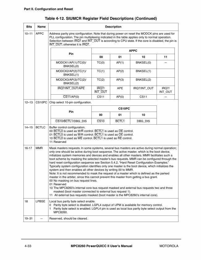
Part II. ConÞguration and Reset
10Ð11 APPC Address parity pins conÞguration. Note that during power on reset the MODCK pins are used for PLL conÞguration. The pin multiplexing indicated in the table applies only to normal operation. Selection between IRQ7 and INT_OUT is according to CPU state. If the core is disabled, the pin is INT_OUT; otherwise it is IRQ7.
Pin APPC
00 01 10 11
MODCK1/AP(1)/TC(0)/BNKSEL(0)
TC(0) AP(1) BNKSEL(0) Ñ
MODCK2/AP(2)/TC(1)/BNKSEL(1)
TC(1) AP(2) BNKSEL(1)
MODCK3/AP(3)/TC(2)/BNKSEL(2)
TC(2) AP(3) BNKSEL(2)
IRQ7/INT_OUT/APE IRQ7/INT_OUT
APE IRQ7/INT_OUT IRQ7/INT_OUT
CS11/AP(0) CS11 AP(0) CS11 Ñ
12Ð13 CS10PC Chip select 10-pin conÞguration.
Pin CS10PC
00 01 10
CS10/BCTL1/DBG_DIS CS10 BCTL1 DBG_DIS
14Ð15 BCTLC Buffer control conÞguration. 00 BCTL0 is used as W/R control. BCTL1 is used as OE control.01 BCTL0 is used as W/R control. BCTL1 is used as OE control.10 BCTL0 is used as WE control. BCTL1 is used as RE control.11 Reserved
16-17 MMR Mask masters requests. In some systems, several bus masters are active during normal operation; only one should be active during boot sequence. The active master, which is the boot device, initializes system memories and devices and enables all other masters. MMR facilitates such a boot scheme by masking the selected masterÕs bus requests. MMR can be conÞgured through the hard reset conÞguration sequence see Section 5.4.2, ÒHard Reset ConÞguration Examples.Ó Typically system conÞguration identiÞes only one master is the boot device, which initializes the system and then enables all other devices by writing 00 to MMR. Note: It is not recommended to mask the request of a master which is deÞned as the parked master in the arbiter, since this cannot prevent this master from getting a bus grant.00 No masking on bus request lines.01 Reserved10 The MPC8260Õs internal core bus request masked and external bus requests two and three
masked (boot master connected to external bus request 1).11 All external bus requests masked (boot master is the MPC8260Õs internal core).
18 LPBSE Local bus parity byte select enable.0 Parity byte select is disabled. LGPL4 output of UPM is available for memory control.1 Parity byte select is enabled. LGPL4 pin is used as local bus parity byte select output from the
MPC8260.
19Ð31 Ñ Reserved, should be cleared.
Table 4-12. SIUMCR Register Field Descriptions (Continued)
Bits Name Description
4-33 MPC8260 PowerQUICC II UserÕs Manual MOTOROLA
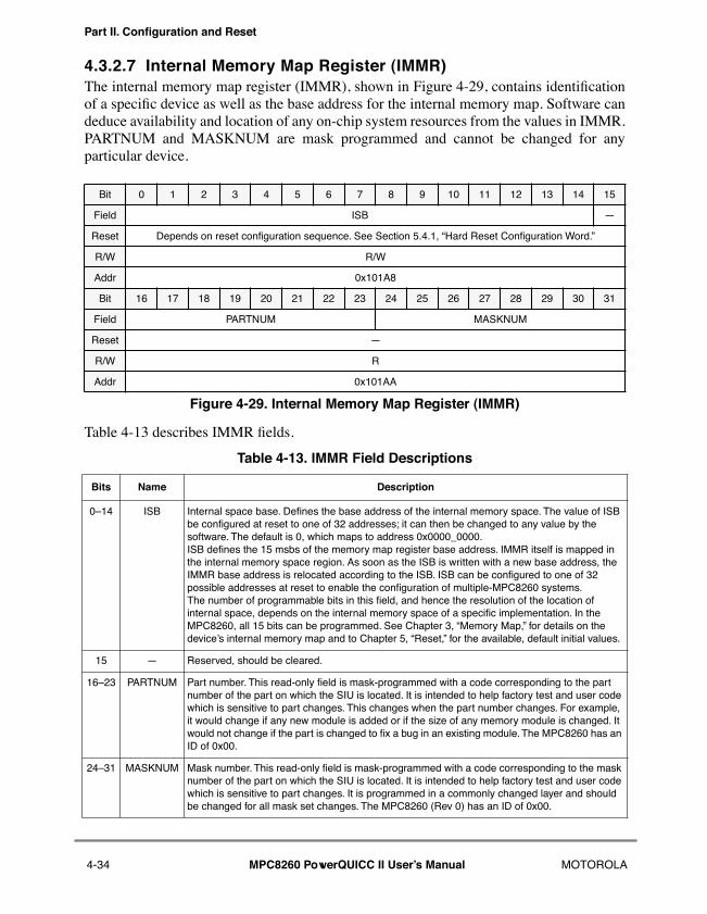
Part II. ConÞguration and Reset
4.3.2.7 Internal Memory Map Register (IMMR)The internal memory map register (IMMR), shown in Figure 4-29, contains identiÞcationof a speciÞc device as well as the base address for the internal memory map. Software candeduce availability and location of any on-chip system resources from the values in IMMR.PARTNUM and MASKNUM are mask programmed and cannot be changed for anyparticular device.
Table 4-13 describes IMMR Þelds.
Bit 0 1 2 3 4 5 6 7 8 9 10 11 12 13 14 15
Field ISB Ñ
Reset Depends on reset conÞguration sequence. See Section 5.4.1, ÒHard Reset ConÞguration Word.Ó
R/W R/W
Addr 0x101A8
Bit 16 17 18 19 20 21 22 23 24 25 26 27 28 29 30 31
Field PARTNUM MASKNUM
Reset Ñ
R/W R
Addr 0x101AA
Figure 4-29. Internal Memory Map Register (IMMR)
Table 4-13. IMMR Field Descriptions
Bits Name Description
0Ð14 ISB Internal space base. DeÞnes the base address of the internal memory space. The value of ISB be conÞgured at reset to one of 32 addresses; it can then be changed to any value by the software. The default is 0, which maps to address 0x0000_0000. ISB deÞnes the 15 msbs of the memory map register base address. IMMR itself is mapped in the internal memory space region. As soon as the ISB is written with a new base address, the IMMR base address is relocated according to the ISB. ISB can be conÞgured to one of 32 possible addresses at reset to enable the conÞguration of multiple-MPC8260 systems.The number of programmable bits in this Þeld, and hence the resolution of the location of internal space, depends on the internal memory space of a speciÞc implementation. In the MPC8260, all 15 bits can be programmed. See Chapter 3, ÒMemory Map,Ó for details on the deviceÕs internal memory map and to Chapter 5, ÒReset,Ó for the available, default initial values.
15 Ñ Reserved, should be cleared.
16Ð23 PARTNUM Part number. This read-only Þeld is mask-programmed with a code corresponding to the part number of the part on which the SIU is located. It is intended to help factory test and user code which is sensitive to part changes. This changes when the part number changes. For example, it would change if any new module is added or if the size of any memory module is changed. It would not change if the part is changed to Þx a bug in an existing module. The MPC8260 has an ID of 0x00.
24Ð31 MASKNUM Mask number. This read-only Þeld is mask-programmed with a code corresponding to the mask number of the part on which the SIU is located. It is intended to help factory test and user code which is sensitive to part changes. It is programmed in a commonly changed layer and should be changed for all mask set changes. The MPC8260 (Rev 0) has an ID of 0x00.
4-34 MPC8260 PowerQUICC II UserÕs Manual MOTOROLA
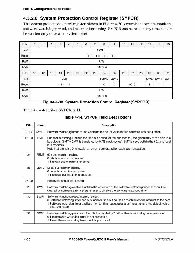
Part II. ConÞguration and Reset
4.3.2.8 System Protection Control Register (SYPCR)The system protection control register, shown in Figure 4-30, controls the system monitors,software watchdog period, and bus monitor timing. SYPCR can be read at any time but canbe written only once after system reset.
Table 4-14 describes SYPCR Þelds.
Bits 0 1 2 3 4 5 6 7 8 9 10 11 12 13 14 15
Field SWTC
Reset 1111_1111_1111_1111
R/W R/W
Addr 0x10004
Bits 16 17 18 19 20 21 22 23 24 25 26 27 28 29 30 31
Field BMT PBME LBME Ñ SWE SWRI SWP
Reset 1111_1111 0 0 00_0 1 1 1
R/W R/W
Addr 0x10006
Figure 4-30. System Protection Control Register (SYPCCR)
Table 4-14. SYPCR Field Descriptions
Bits Name Description
0Ð15 SWTC Software watchdog timer count. Contains the count value for the software watchdog timer.
16Ð23 BMT Bus monitor timing. DeÞnes the time-out period for the bus monitor, the granularity of this Þeld is 8 bus clocks. (BMT = 0xFF is translated to 0x7f8 clock cycles). BMT is used both in the 60x and local bus monitors.Note that the value 0 in invalid; an error is generated for each bus transaction.
24 PBME 60x bus monitor enable. 0 60x bus monitor is disabled.1 The 60x bus monitor is enabled.
25 LBME Local bus monitor enable. 0 Local bus monitor is disabled.1 The local bus monitor is enabled.
26Ð29 Ñ Reserved, should be cleared.
29 SWE Software watchdog enable. Enables the operation of the software watchdog timer. It should be cleared by software after a system reset to disable the software watchdog timer.
30 SWRI Software watchdog reset/interrupt select. 0 Software watchdog timer and bus monitor time-out causes a machine check interrupt to the core. 1 Software watchdog timer and bus monitor time-out causes a soft reset (this is the default value
after soft reset).
31 SWP Software watchdog prescale. Controls the divide-by-2,048 software watchdog timer prescaler. 0 The software watchdog timer is not prescaled. 1 The software watchdog timer clock is prescaled.
4-35 MPC8260 PowerQUICC II UserÕs Manual MOTOROLA
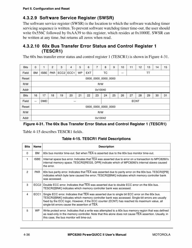
Part II. ConÞguration and Reset
4.3.2.9 Software Service Register (SWSR)The software service register (SWSR) is the location to which the software watchdog timerservicing sequence is written. To prevent software watchdog timer time-out, the user shouldwrite 0x556C followed by 0xAA39 to this register, which resides at 0x1000E. SWSR canbe written at any time, but returns all zeros when read.
4.3.2.10 60x Bus Transfer Error Status and Control Register 1 (TESCR1)
The 60x bus transfer error status and control register 1 (TESCR1) is shown in Figure 4-31.
Table 4-15 describes TESCR1 Þelds.
Bits 0 1 2 3 4 5 6 7 8 9 10 11 12 13 14 15
Field BM ISBE PAR ECC2 ECC1 WP EXT TC Ñ TT
Reset 0000_0000_0000_0000
R/W R/W
Addr 0x10040
Bits 16 17 18 19 20 21 22 23 24 25 26 27 28 29 30 31
Field Ñ DMD Ñ ECNT
Reset 0000_0000_0000_0000
R/W R/W
Addr 0x10042
Figure 4-31. The 60x Bus Transfer Error Status and Control Register 1 (TESCR1)
Table 4-15. TESCR1 Field Descriptions
Bits Name Description
0 BM 60x bus monitor time-out. Set when TEA is asserted due to the 60x bus monitor time-out.
1 ISBE Internal space bus error. Indicates that TEA was asserted due to error on a transaction to MPC8260Õs internal memory space. TESCR2[REGS, DPR] indicate which of MPC8260Õs internal slaves caused the error.
2 PAR 60x bus parity error. Indicates that TEA was asserted due to parity error on the 60x bus. TESCR2[PB] indicates which byte lane caused the error; TESCR2[BNK] indicates which memory controller bank was accessed.
3 ECC2 Double ECC error. Indicates that TEA was asserted due to double ECC error on the 60x bus. TESCR2[BNK] indicates which memory controller bank was accessed.
4 ECC1 Single ECC error. Indicates that TEA was asserted due to single bit ECC error on the 60x bus. TESCR2[BNK] indicates which memory controller bank was accessed. Single-bit errors are usually Þxed by the ECC logic. However, if the ECC counter (ECNT) has reached its maximum value, all single-bit errors cause the assertion of TEA.
5 WP Write protect error. Indicates that a write was attempted to a 60x bus memory region that was deÞned as read-only in the memory controller. Note that this alone does not cause TEA assertion. Usually, in this case, the bus monitor will time-out.
4-36 MPC8260 PowerQUICC II UserÕs Manual MOTOROLA
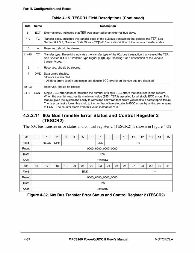
Part II. ConÞguration and Reset
4.3.2.11 60x Bus Transfer Error Status and Control Register 2 (TESCR2)
The 60x bus transfer error status and control register 2 (TESCR2) is shown in Figure 4-32.
6 EXT External error. Indicates that TEA was asserted by an external bus slave.
7Ð9 TC Transfer code. Indicates the transfer code of the 60x bus transaction that caused the TEA. See Section 8.4.3.2, ÒTransfer Code Signals TC[0Ð2],Ó for a description of the various transfer codes.
10 Ñ Reserved, should be cleared.
11Ð15 TT Transfer type. These bits indicates the transfer type of the 60x bus transaction that caused the TEA. See Section 8.4.3.1, ÒTransfer Type Signal (TT[0Ð4]) Encoding,Ó for a description of the various transfer types.
16 Ñ Reserved, should be cleared.
17 DMD Data errors disable.0 Errors are enabled.1 All data errors (parity and single and double ECC errors) on the 60x bus are disabled.
18Ð23 Ñ Reserved, should be cleared.
24Ð31 ECNT Single ECC error counter.Indicates the number of single ECC errors that occurred in the system. When the counter reaches its maximum value (255), TEA is asserted for all single ECC errors. This feature gives the system the ability to withstand a few random errors yet react to a catastrophic failure. The user can set a lower threshold to the number of tolerated single ECC errors by writing some value to ECNT. The counter starts from this value instead of zero.
Bits 0 1 2 3 4 5 6 7 8 9 10 11 12 13 14 15
Field Ñ REGS DPR Ñ LCL PB
Reset 0000_0000_0000_0000
R/W R/W
Addr 0x10044
Bits 16 17 18 19 20 21 22 23 24 25 26 27 28 29 30 31
Field BNK Ñ
Reset 0000_0000_0000_0000
R/W R/W
Addr 0x10046
Figure 4-32. 60x Bus Transfer Error Status and Control Register 2 (TESCR2)
Table 4-15. TESCR1 Field Descriptions (Continued)
Bits Name Description
4-37 MPC8260 PowerQUICC II UserÕs Manual MOTOROLA
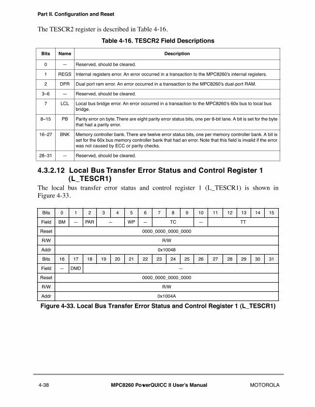
Part II. ConÞguration and Reset
The TESCR2 register is described in Table 4-16.
4.3.2.12 Local Bus Transfer Error Status and Control Register 1 (L_TESCR1)
The local bus transfer error status and control register 1 (L_TESCR1) is shown inFigure 4-33.
Table 4-16. TESCR2 Field Descriptions
Bits Name Description
0 Ñ Reserved, should be cleared.
1 REGS Internal registers error. An error occurred in a transaction to the MPC8260Õs internal registers.
2 DPR Dual port ram error. An error occurred in a transaction to the MPC8260Õs dual-port RAM.
3Ð6 Ñ Reserved, should be cleared.
7 LCL Local bus bridge error. An error occurred in a transaction to the MPC8260Õs 60x bus to local bus bridge.
8Ð15 PB Parity error on byte. There are eight parity error status bits, one per 8-bit lane. A bit is set for the byte that had a parity error.
16Ð27 BNK Memory controller bank. There are twelve error status bits, one per memory controller bank. A bit is set for the 60x bus memory controller bank that had an error. Note that this Þeld is invalid if the error was not caused by ECC or parity checks.
28Ð31 Ñ Reserved, should be cleared.
Bits 0 1 2 3 4 5 6 7 8 9 10 11 12 13 14 15
Field BM Ñ PAR Ñ WP Ñ TC Ñ TT
Reset 0000_0000_0000_0000
R/W R/W
Addr 0x10048
Bits 16 17 18 19 20 21 22 23 24 25 26 27 28 29 30 31
Field Ñ DMD Ñ
Reset 0000_0000_0000_0000
R/W R/W
Addr 0x1004A
Figure 4-33. Local Bus Transfer Error Status and Control Register 1 (L_TESCR1)
4-38 MPC8260 PowerQUICC II UserÕs Manual MOTOROLA
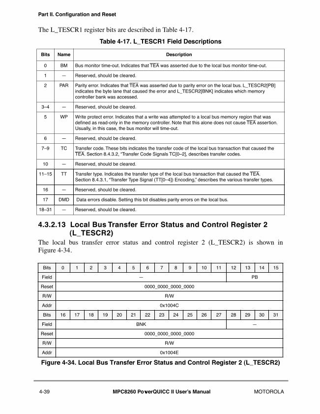
Part II. ConÞguration and Reset
The L_TESCR1 register bits are described in Table 4-17.
4.3.2.13 Local Bus Transfer Error Status and Control Register 2 (L_TESCR2)
The local bus transfer error status and control register 2 (L_TESCR2) is shown inFigure 4-34.
Table 4-17. L_TESCR1 Field Descriptions
Bits Name Description
0 BM Bus monitor time-out. Indicates that TEA was asserted due to the local bus monitor time-out.
1 Ñ Reserved, should be cleared.
2 PAR Parity error. Indicates that TEA was asserted due to parity error on the local bus. L_TESCR2[PB] indicates the byte lane that caused the error and L_TESCR2[BNK] indicates which memory controller bank was accessed.
3Ð4 Ñ Reserved, should be cleared.
5 WP Write protect error. Indicates that a write was attempted to a local bus memory region that was deÞned as read-only in the memory controller. Note that this alone does not cause TEA assertion. Usually, in this case, the bus monitor will time-out.
6 Ñ Reserved, should be cleared.
7Ð9 TC Transfer code. These bits indicates the transfer code of the local bus transaction that caused the TEA. Section 8.4.3.2, ÒTransfer Code Signals TC[0Ð2], describes transfer codes.
10 Ñ Reserved, should be cleared.
11Ð15 TT Transfer type. Indicates the transfer type of the local bus transaction that caused the TEA. Section 8.4.3.1, ÒTransfer Type Signal (TT[0Ð4]) Encoding,Ó describes the various transfer types.
16 Ñ Reserved, should be cleared.
17 DMD Data errors disable. Setting this bit disables parity errors on the local bus.
18Ð31 Ñ Reserved, should be cleared.
Bits 0 1 2 3 4 5 6 7 8 9 10 11 12 13 14 15
Field Ñ PB
Reset 0000_0000_0000_0000
R/W R/W
Addr 0x1004C
Bits 16 17 18 19 20 21 22 23 24 25 26 27 28 29 30 31
Field BNK Ñ
Reset 0000_0000_0000_0000
R/W R/W
Addr 0x1004E
Figure 4-34. Local Bus Transfer Error Status and Control Register 2 (L_TESCR2)
4-39 MPC8260 PowerQUICC II UserÕs Manual MOTOROLA
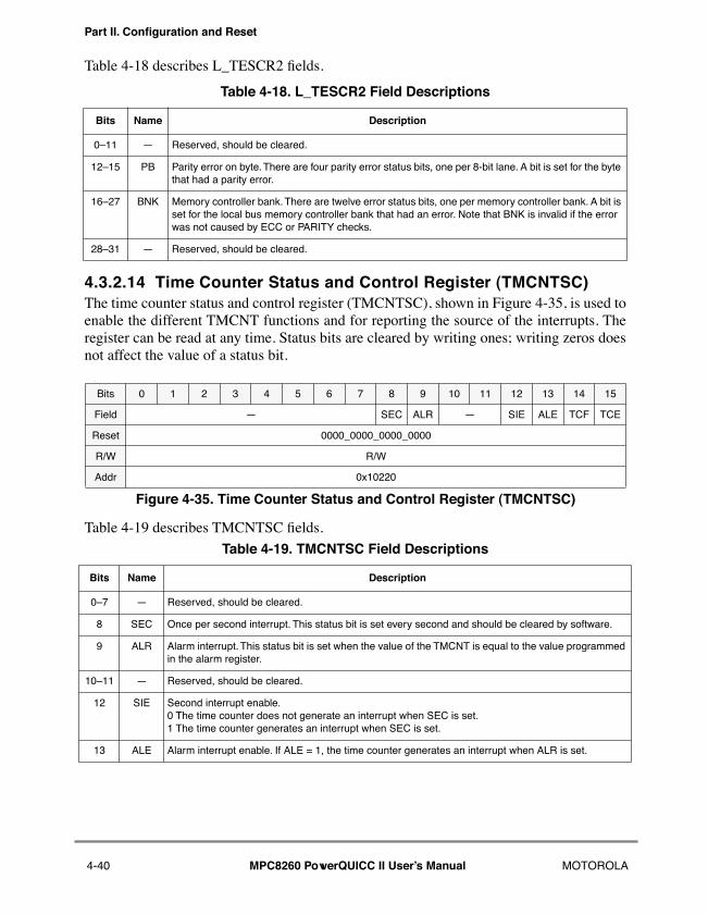
Part II. ConÞguration and Reset
Table 4-18 describes L_TESCR2 Þelds.
4.3.2.14 Time Counter Status and Control Register (TMCNTSC)The time counter status and control register (TMCNTSC), shown in Figure 4-35, is used toenable the different TMCNT functions and for reporting the source of the interrupts. Theregister can be read at any time. Status bits are cleared by writing ones; writing zeros doesnot affect the value of a status bit.
.
Table 4-19 describes TMCNTSC Þelds.
Table 4-18. L_TESCR2 Field Descriptions
Bits Name Description
0Ð11 Ñ Reserved, should be cleared.
12Ð15 PB Parity error on byte. There are four parity error status bits, one per 8-bit lane. A bit is set for the byte that had a parity error.
16Ð27 BNK Memory controller bank. There are twelve error status bits, one per memory controller bank. A bit is set for the local bus memory controller bank that had an error. Note that BNK is invalid if the error was not caused by ECC or PARITY checks.
28Ð31 Ñ Reserved, should be cleared.
Bits 0 1 2 3 4 5 6 7 8 9 10 11 12 13 14 15
Field Ñ SEC ALR Ñ SIE ALE TCF TCE
Reset 0000_0000_0000_0000
R/W R/W
Addr 0x10220
Figure 4-35. Time Counter Status and Control Register (TMCNTSC)
Table 4-19. TMCNTSC Field Descriptions
Bits Name Description
0Ð7 Ñ Reserved, should be cleared.
8 SEC Once per second interrupt. This status bit is set every second and should be cleared by software.
9 ALR Alarm interrupt. This status bit is set when the value of the TMCNT is equal to the value programmed in the alarm register.
10Ð11 Ñ Reserved, should be cleared.
12 SIE Second interrupt enable. 0 The time counter does not generate an interrupt when SEC is set.1 The time counter generates an interrupt when SEC is set.
13 ALE Alarm interrupt enable. If ALE = 1, the time counter generates an interrupt when ALR is set.
4-40 MPC8260 PowerQUICC II UserÕs Manual MOTOROLA
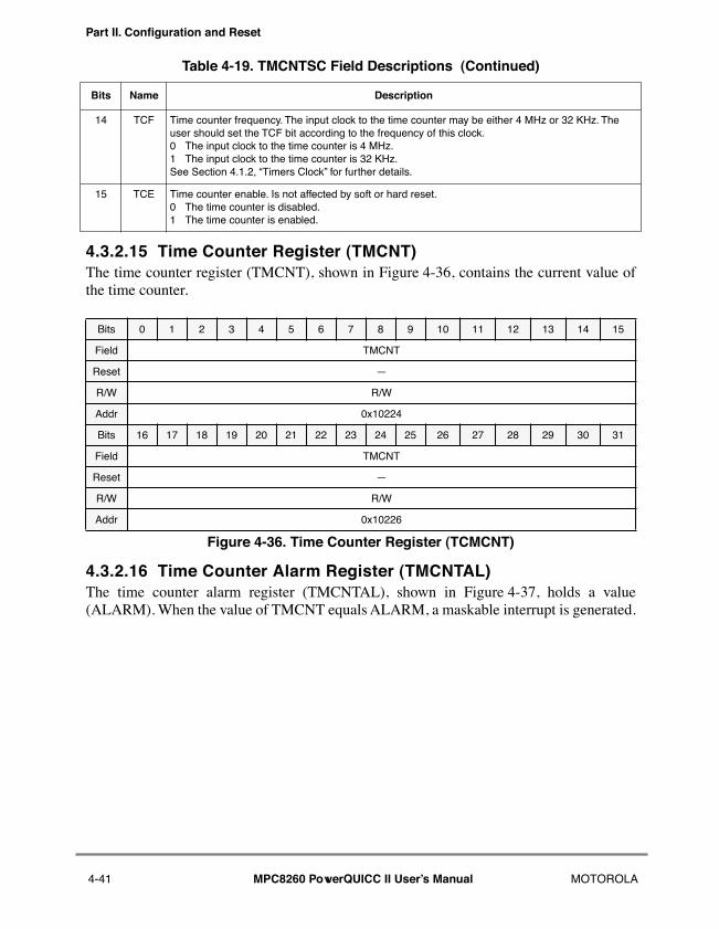
Part II. ConÞguration and Reset
4.3.2.15 Time Counter Register (TMCNT)The time counter register (TMCNT), shown in Figure 4-36, contains the current value ofthe time counter.
4.3.2.16 Time Counter Alarm Register (TMCNTAL)The time counter alarm register (TMCNTAL), shown in Figure 4-37, holds a value(ALARM). When the value of TMCNT equals ALARM, a maskable interrupt is generated.
14 TCF Time counter frequency. The input clock to the time counter may be either 4 MHz or 32 KHz. The user should set the TCF bit according to the frequency of this clock. 0 The input clock to the time counter is 4 MHz. 1 The input clock to the time counter is 32 KHz.See Section 4.1.2, ÒTimers ClockÓ for further details.
15 TCE Time counter enable. Is not affected by soft or hard reset.0 The time counter is disabled. 1 The time counter is enabled.
Bits 0 1 2 3 4 5 6 7 8 9 10 11 12 13 14 15
Field TMCNT
Reset Ñ
R/W R/W
Addr 0x10224
Bits 16 17 18 19 20 21 22 23 24 25 26 27 28 29 30 31
Field TMCNT
Reset Ñ
R/W R/W
Addr 0x10226
Figure 4-36. Time Counter Register (TCMCNT)
Table 4-19. TMCNTSC Field Descriptions (Continued)
Bits Name Description
4-41 MPC8260 PowerQUICC II UserÕs Manual MOTOROLA
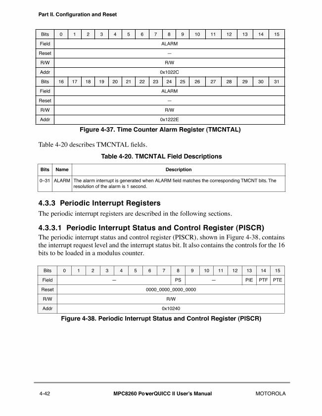
Part II. ConÞguration and Reset
Table 4-20 describes TMCNTAL Þelds.
4.3.3 Periodic Interrupt RegistersThe periodic interrupt registers are described in the following sections.
4.3.3.1 Periodic Interrupt Status and Control Register (PISCR)The periodic interrupt status and control register (PISCR), shown in Figure 4-38, containsthe interrupt request level and the interrupt status bit. It also contains the controls for the 16bits to be loaded in a modulus counter.
Bits 0 1 2 3 4 5 6 7 8 9 10 11 12 13 14 15
Field ALARM
Reset Ñ
R/W R/W
Addr 0x1022C
Bits 16 17 18 19 20 21 22 23 24 25 26 27 28 29 30 31
Field ALARM
Reset Ñ
R/W R/W
Addr 0x1222E
Figure 4-37. Time Counter Alarm Register (TMCNTAL)
Table 4-20. TMCNTAL Field Descriptions
Bits Name Description
0Ð31 ALARM The alarm interrupt is generated when ALARM Þeld matches the corresponding TMCNT bits. The resolution of the alarm is 1 second.
Bits 0 1 2 3 4 5 6 7 8 9 10 11 12 13 14 15
Field Ñ PS Ñ PIE PTF PTE
Reset 0000_0000_0000_0000
R/W R/W
Addr 0x10240
Figure 4-38. Periodic Interrupt Status and Control Register (PISCR)
4-42 MPC8260 PowerQUICC II UserÕs Manual MOTOROLA
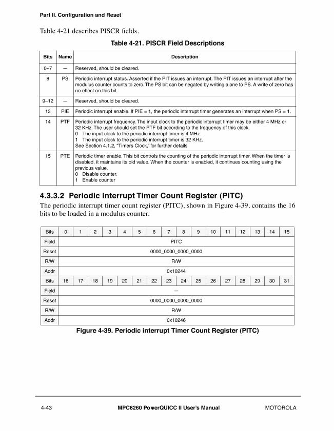
Part II. ConÞguration and Reset
Table 4-21 describes PISCR Þelds.
4.3.3.2 Periodic Interrupt Timer Count Register (PITC)The periodic interrupt timer count register (PITC), shown in Figure 4-39, contains the 16bits to be loaded in a modulus counter.
Table 4-21. PISCR Field Descriptions
Bits Name Description
0Ð7 Ñ Reserved, should be cleared.
8 PS Periodic interrupt status. Asserted if the PIT issues an interrupt. The PIT issues an interrupt after the modulus counter counts to zero. The PS bit can be negated by writing a one to PS. A write of zero has no effect on this bit.
9Ð12 Ñ Reserved, should be cleared.
13 PIE Periodic interrupt enable. If PIE = 1, the periodic interrupt timer generates an interrupt when PS = 1.
14 PTF Periodic interrupt frequency. The input clock to the periodic interrupt timer may be either 4 MHz or 32 KHz. The user should set the PTF bit according to the frequency of this clock. 0 The input clock to the periodic interrupt timer is 4 MHz. 1 The input clock to the periodic interrupt timer is 32 KHz.See Section 4.1.2, ÒTimers Clock,Ó for further details
15 PTE Periodic timer enable. This bit controls the counting of the periodic interrupt timer. When the timer is disabled, it maintains its old value. When the counter is enabled, it continues counting using the previous value.0 Disable counter.1 Enable counter
Bits 0 1 2 3 4 5 6 7 8 9 10 11 12 13 14 15
Field PITC
Reset 0000_0000_0000_0000
R/W R/W
Addr 0x10244
Bits 16 17 18 19 20 21 22 23 24 25 26 27 28 29 30 31
Field Ñ
Reset 0000_0000_0000_0000
R/W R/W
Addr 0x10246
Figure 4-39. Periodic interrupt Timer Count Register (PITC)
4-43 MPC8260 PowerQUICC II UserÕs Manual MOTOROLA
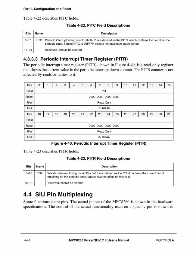
Part II. ConÞguration and Reset
Table 4-22 describes PITC Þelds.
4.3.3.3 Periodic Interrupt Timer Register (PITR)The periodic interrupt timer register (PITR), shown in Figure 4-40, is a read-only registerthat shows the current value in the periodic interrupt down counter. The PITR counter is notaffected by reads or writes to it.
Table 4-23 describes PITR Þelds.
4.4 SIU Pin MultiplexingSome functions share pins. The actual pinout of the MPC8260 is shown in the hardwarespeciÞcations. The control of the actual functionality used on a speciÞc pin is shown in
Table 4-22. PITC Field Descriptions
Bits Name Description
0Ð15 PITC Periodic interrupt timing count. Bits 0Ð15 are deÞned as the PITC, which contains the count for the periodic timer. Setting PITC to 0xFFFF selects the maximum count period.
16Ð31 Ñ Reserved, should be cleared.
Bits 0 1 2 3 4 5 6 7 8 9 10 11 12 13 14 15
Field PIT
Reset 0000_0000_0000_0000
R/W Read Only
Addr 0x10248
Bits 16 17 18 19 20 21 22 23 24 25 26 27 28 29 30 31
Field Ñ
Reset 0000_0000_0000_0000
R/W Read Only
Addr 0x1024A
Figure 4-40. Periodic Interrupt Timer Register (PITR)
Table 4-23. PITR Field Descriptions
Bits Name Description
0Ð15 PITC Periodic interrupt timing count. Bits 0Ð15 are deÞned as the PIT. It contains the current count remaining for the periodic timer. Writes have no effect on this Þeld.
16Ð31 Ñ Reserved, should be cleared.
4-44 MPC8260 PowerQUICC II UserÕs Manual MOTOROLA
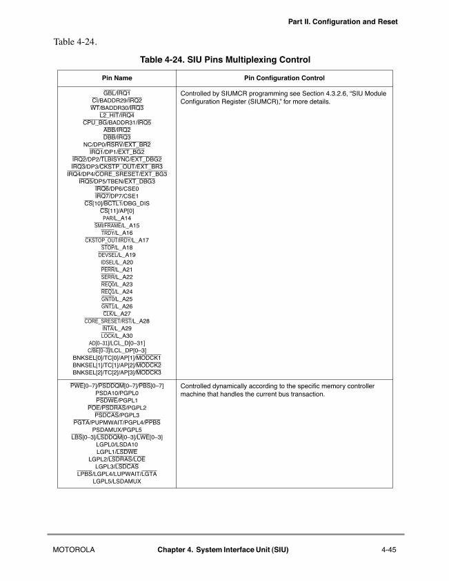
Part II. ConÞguration and Reset
Table 4-24.
Table 4-24. SIU Pins Multiplexing Control
Pin Name Pin ConÞguration Control
GBL/IRQ1CI/BADDR29/IRQ2WT/BADDR30/IRQ3
L2_HIT/IRQ4CPU_BG/BADDR31/IRQ5
ABB/IRQ2DBB/IRQ3
NC/DP0/RSRV/EXT_BR2IRQ1/DP1/EXT_BG2
IRQ2/DP2/TLBISYNC/EXT_DBG2IRQ3/DP3/CKSTP_OUT/EXT_BR3
IRQ4/DP4/CORE_SRESET/EXT_BG3IRQ5/DP5/TBEN/EXT_DBG3
IRQ6/DP6/CSE0IRQ7/DP7/CSE1
CS[10]/BCTL1/DBG_DISCS[11]/AP[0]
PAR/L_A14SMI/FRAME/L_A15
TRDY/L_A16CKSTOP_OUT/IRDY/L_A17
STOP/L_A18DEVSEL/L_A19IDSEL/L_A20PERR/L_A21SERR/L_A22REQ0/L_A23REQ1/L_A24GNT0/L_A25GNT1/L_A26CLK/L_A27
CORE_SRESET/RST/L_A28INTA/L_A29LOCK/L_A30
AD[0–31]/LCL_D[0Ð31]C/BE[0–3]/LCL_DP[0Ð3]
BNKSEL[0]/TC[0]/AP[1]/MODCK1BNKSEL[1]/TC[1]/AP[2]/MODCK2BNKSEL[2]/TC[2]/AP[3]/MODCK3
Controlled by SIUMCR programming see Section 4.3.2.6, ÒSIU Module ConÞguration Register (SIUMCR),Ó for more details.
PWE[0Ð7]/PSDDQM[0Ð7]/PBS[0Ð7]PSDA10/PGPL0PSDWE/PGPL1
POE/PSDRAS/PGPL2PSDCAS/PGPL3
PGTA/PUPMWAIT/PGPL4/PPBSPSDAMUX/PGPL5
LBS[0Ð3]/LSDDQM[0Ð3]/LWE[0Ð3]LGPL0/LSDA10LGPL1/LSDWE
LGPL2/LSDRAS/LOELGPL3/LSDCAS
LPBS/LGPL4/LUPWAIT/LGTALGPL5/LSDAMUX
Controlled dynamically according to the speciÞc memory controller machine that handles the current bus transaction.
MOTOROLA Chapter 4. System Interface Unit (SIU) 4-45

Part II. ConÞguration and Reset
4-46 MPC8260 PowerQUICC II UserÕs Manual MOTOROLA
Chapter 5 Reset5050
The MPC8260 has several inputs to the reset logic:
¥ Power-on reset (PORESET)¥ External hard reset (HRESET)¥ External soft reset (SRESET)¥ Software watchdog reset¥ Bus monitor reset¥ Checkstop reset¥ JTAG reset
All of these reset sources are fed into the reset controller and, depending on the source ofthe reset, different actions are taken. The reset status register, described in Section 5.2,ÒReset Status Register (RSR),Ó indicates the last sources to cause a reset.
5.1 Reset CausesTable 5-1 describes reset causes.
Table 5-1. Reset Causes
Name Description
Power-on reset(PORESET)
Input pin. Asserting this pin initiates the power-on reset ßow that resets all the chip and conÞgures various attributes of the chip including its clock mode.
Hard reset (HRESET)
This is a bidirectional I/O pin. The MPC8260 can detect an external assertion of HRESET only if it occurs while the MPC8260 is not asserting reset. During HRESET, SRESET is asserted. HRESET is an open-collector pin.
Soft reset (SRESET)
Bidirectional I/O pin. The MPC8260 can only detect an external assertion of SRESET if it occurs while the MPC8260 is not asserting reset. SRESET is an open-drain pin.
Software watchdog reset
After the MPC8260Õs watchdog counts to zero, a software watchdog reset is signaled. The enabled software watchdog event then generates an internal hard reset sequence.
Bus monitor reset
After the MPC8260s bus monitor counts to zero, a bus monitor reset is asserted. The enabled bus monitor event then generates an internal hard reset sequence.
Checkstop reset
If the core enters checkstop state and the checkstop reset is enabled (RMR[CSRE] = 1), the checkstop reset is asserted. The enabled checkstop event then generates an internal hard reset sequence.
JTAG reset When JTAG logic asserts the JTAG soft reset signal, an internal soft reset sequence is generated.
MOTOROLA Chapter 5. Reset 5-1
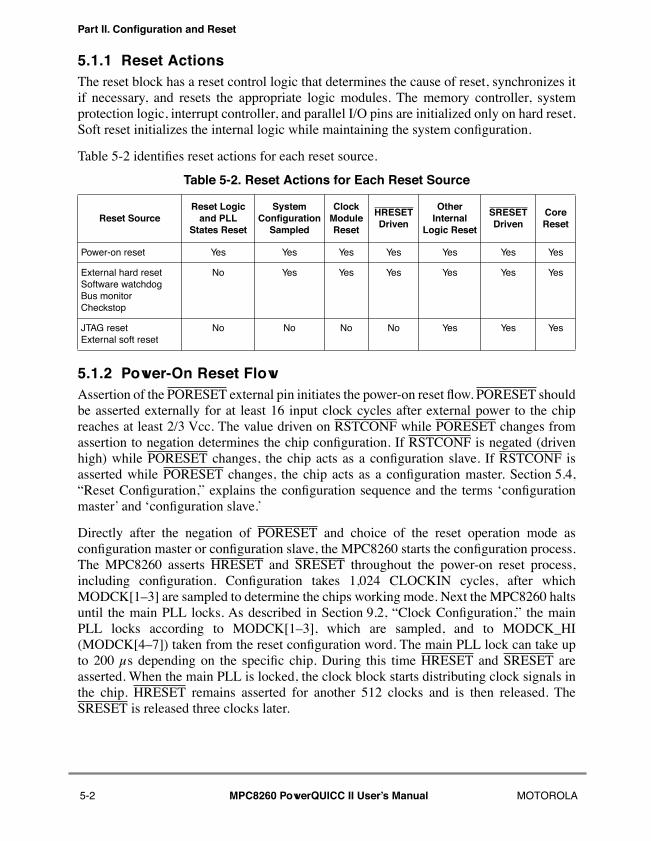
Part II. ConÞguration and Reset
5.1.1 Reset ActionsThe reset block has a reset control logic that determines the cause of reset, synchronizes itif necessary, and resets the appropriate logic modules. The memory controller, systemprotection logic, interrupt controller, and parallel I/O pins are initialized only on hard reset.Soft reset initializes the internal logic while maintaining the system conÞguration.
Table 5-2 identiÞes reset actions for each reset source.
5.1.2 Power-On Reset FlowAssertion of the PORESET external pin initiates the power-on reset ßow. PORESET shouldbe asserted externally for at least 16 input clock cycles after external power to the chipreaches at least 2/3 Vcc. The value driven on RSTCONF while PORESET changes fromassertion to negation determines the chip conÞguration. If RSTCONF is negated (drivenhigh) while PORESET changes, the chip acts as a conÞguration slave. If RSTCONF isasserted while PORESET changes, the chip acts as a conÞguration master. Section 5.4,ÒReset ConÞguration,Ó explains the conÞguration sequence and the terms ÔconÞgurationmasterÕ and ÔconÞguration slave.Õ
Directly after the negation of PORESET and choice of the reset operation mode asconÞguration master or conÞguration slave, the MPC8260 starts the conÞguration process.The MPC8260 asserts HRESET and SRESET throughout the power-on reset process,including conÞguration. ConÞguration takes 1,024 CLOCKIN cycles, after whichMODCK[1Ð3] are sampled to determine the chips working mode. Next the MPC8260 haltsuntil the main PLL locks. As described in Section 9.2, ÒClock ConÞguration,Ó the mainPLL locks according to MODCK[1Ð3], which are sampled, and to MODCK_HI(MODCK[4Ð7]) taken from the reset conÞguration word. The main PLL lock can take upto 200 µs depending on the speciÞc chip. During this time HRESET and SRESET areasserted. When the main PLL is locked, the clock block starts distributing clock signals inthe chip. HRESET remains asserted for another 512 clocks and is then released. TheSRESET is released three clocks later.
Table 5-2. Reset Actions for Each Reset Source
Reset SourceReset Logic
and PLL States Reset
System ConÞguration
Sampled
Clock Module Reset
HRESET Driven
Other Internal
Logic Reset
SRESET Driven
Core Reset
Power-on reset Yes Yes Yes Yes Yes Yes Yes
External hard resetSoftware watchdogBus monitorCheckstop
No Yes Yes Yes Yes Yes Yes
JTAG resetExternal soft reset
No No No No Yes Yes Yes
5-2 MPC8260 PowerQUICC II UserÕs Manual MOTOROLA
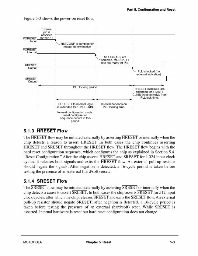
Part II. ConÞguration and Reset
Figure 5-3 shows the power-on reset ßow.
5.1.3 HRESET FlowThe HRESET ßow may be initiated externally by asserting HRESET or internally when thechip detects a reason to assert HRESET. In both cases the chip continues assertingHRESET and SRESET throughout the HRESET ßow. The HRESET ßow begins with thehard reset conÞguration sequence, which conÞgures the chip as explained in Section 5.4,ÒReset ConÞguration.Ó After the chip asserts HRESET and SRESET for 1,024 input clockcycles, it releases both signals and exits the HRESET ßow. An external pull-up resistorshould negate the signals. After negation is detected, a 16-cycle period is taken beforetesting the presence of an external (hard/soft) reset.
5.1.4 SRESET FlowThe SRESET ßow may be initiated externally by asserting SRESET or internally when thechip detects a cause to assert SRESET. In both cases the chip asserts SRESET for 512 inputclock cycles, after which the chip releases SRESET and exits the SRESET ßow. An externalpull-up resistor should negate SRESET; after negation is detected, a 16-cycle period istaken before testing the presence of an external (hard/soft) reset. While SRESET isasserted, internal hardware is reset but hard reset conÞguration does not change.
PORESET
PORESET Internal
HRESET
Input
Output
SRESETOutput
External pin is
asserted for min 16
RSTCONF is sampled for master determination
MODCK[1Ð3] are sampled. MODCK_HI bits are ready for PLL
PLL is locked (no external indication)
HRESET /SRESET are extended for 512/515
CLKIN (respectively), from PLL lock time.
PLL locking period
PORESET to internal logic is extended for 1024 CLKIN.
In reset conÞguration mode: reset conÞguration
sequence occurs in this period.
Interval depends on PLL locking time.
MOTOROLA Chapter 5. Reset 5-3
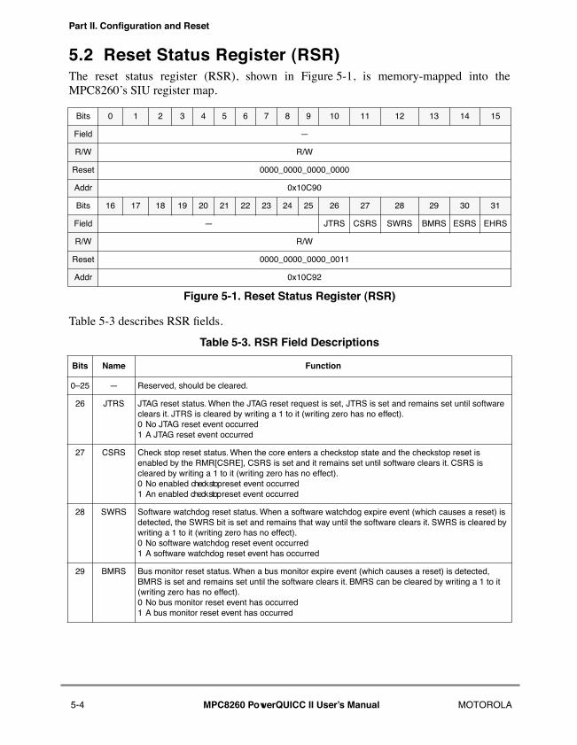
Part II. ConÞguration and Reset
5.2 Reset Status Register (RSR)The reset status register (RSR), shown in Figure 5-1, is memory-mapped into theMPC8260Õs SIU register map.
Table 5-3 describes RSR Þelds.
Bits 0 1 2 3 4 5 6 7 8 9 10 11 12 13 14 15
Field Ñ
R/W R/W
Reset 0000_0000_0000_0000
Addr 0x10C90
Bits 16 17 18 19 20 21 22 23 24 25 26 27 28 29 30 31
Field Ñ JTRS CSRS SWRS BMRS ESRS EHRS
R/W R/W
Reset 0000_0000_0000_0011
Addr 0x10C92
Figure 5-1. Reset Status Register (RSR)
Table 5-3. RSR Field Descriptions
Bits Name Function
0Ð25 Ñ Reserved, should be cleared.
26 JTRS JTAG reset status. When the JTAG reset request is set, JTRS is set and remains set until software clears it. JTRS is cleared by writing a 1 to it (writing zero has no effect).0 No JTAG reset event occurred1 A JTAG reset event occurred
27 CSRS Check stop reset status. When the core enters a checkstop state and the checkstop reset is enabled by the RMR[CSRE], CSRS is set and it remains set until software clears it. CSRS is cleared by writing a 1 to it (writing zero has no effect).0 No enabled check stop reset event occurred1 An enabled check stop reset event occurred
28 SWRS Software watchdog reset status. When a software watchdog expire event (which causes a reset) is detected, the SWRS bit is set and remains that way until the software clears it. SWRS is cleared by writing a 1 to it (writing zero has no effect).0 No software watchdog reset event occurred1 A software watchdog reset event has occurred
29 BMRS Bus monitor reset status. When a bus monitor expire event (which causes a reset) is detected, BMRS is set and remains set until the software clears it. BMRS can be cleared by writing a 1 to it (writing zero has no effect).0 No bus monitor reset event has occurred1 A bus monitor reset event has occurred
5-4 MPC8260 PowerQUICC II UserÕs Manual MOTOROLA
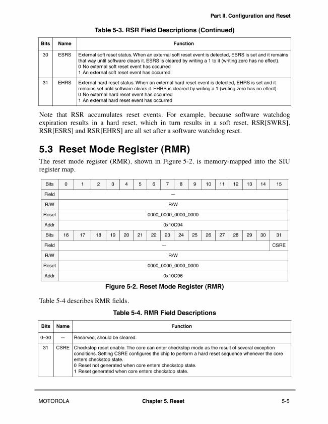
Part II. ConÞguration and Reset
Note that RSR accumulates reset events. For example, because software watchdogexpiration results in a hard reset, which in turn results in a soft reset, RSR[SWRS],RSR[ESRS] and RSR[EHRS] are all set after a software watchdog reset.
5.3 Reset Mode Register (RMR)The reset mode register (RMR), shown in Figure 5-2, is memory-mapped into the SIUregister map.
Table 5-4 describes RMR Þelds.
30 ESRS External soft reset status. When an external soft reset event is detected, ESRS is set and it remains that way until software clears it. ESRS is cleared by writing a 1 to it (writing zero has no effect).0 No external soft reset event has occurred1 An external soft reset event has occurred
31 EHRS External hard reset status. When an external hard reset event is detected, EHRS is set and it remains set until software clears it. EHRS is cleared by writing a 1 (writing zero has no effect).0 No external hard reset event has occurred1 An external hard reset event has occurred
Bits 0 1 2 3 4 5 6 7 8 9 10 11 12 13 14 15
Field Ñ
R/W R/W
Reset 0000_0000_0000_0000
Addr 0x10C94
Bits 16 17 18 19 20 21 22 23 24 25 26 27 28 29 30 31
Field Ñ CSRE
R/W R/W
Reset 0000_0000_0000_0000
Addr 0x10C96
Figure 5-2. Reset Mode Register (RMR)
Table 5-4. RMR Field Descriptions
Bits Name Function
0Ð30 Ñ Reserved, should be cleared.
31 CSRE Checkstop reset enable. The core can enter checkstop mode as the result of several exception conditions. Setting CSRE conÞgures the chip to perform a hard reset sequence whenever the core enters checkstop state.0 Reset not generated when core enters checkstop state.1 Reset generated when core enters checkstop state.
Table 5-3. RSR Field Descriptions (Continued)
Bits Name Function
MOTOROLA Chapter 5. Reset 5-5
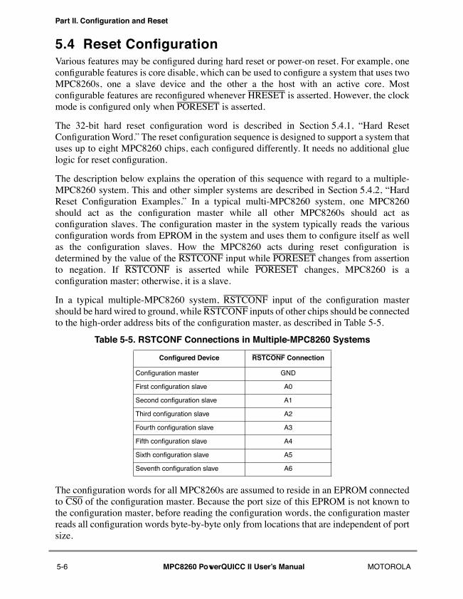
Part II. ConÞguration and Reset
5.4 Reset ConÞgurationVarious features may be conÞgured during hard reset or power-on reset. For example, oneconÞgurable features is core disable, which can be used to conÞgure a system that uses twoMPC8260s, one a slave device and the other a the host with an active core. MostconÞgurable features are reconÞgured whenever HRESET is asserted. However, the clockmode is conÞgured only when PORESET is asserted.
The 32-bit hard reset conÞguration word is described in Section 5.4.1, ÒHard ResetConÞguration Word.Ó The reset conÞguration sequence is designed to support a system thatuses up to eight MPC8260 chips, each conÞgured differently. It needs no additional gluelogic for reset conÞguration.
The description below explains the operation of this sequence with regard to a multiple-MPC8260 system. This and other simpler systems are described in Section 5.4.2, ÒHardReset ConÞguration Examples.Ó In a typical multi-MPC8260 system, one MPC8260should act as the conÞguration master while all other MPC8260s should act asconÞguration slaves. The conÞguration master in the system typically reads the variousconÞguration words from EPROM in the system and uses them to conÞgure itself as wellas the conÞguration slaves. How the MPC8260 acts during reset conÞguration isdetermined by the value of the RSTCONF input while PORESET changes from assertionto negation. If RSTCONF is asserted while PORESET changes, MPC8260 is aconÞguration master; otherwise, it is a slave.
In a typical multiple-MPC8260 system, RSTCONF input of the conÞguration mastershould be hard wired to ground, while RSTCONF inputs of other chips should be connectedto the high-order address bits of the conÞguration master, as described in Table 5-5.
The conÞguration words for all MPC8260s are assumed to reside in an EPROM connectedto CS0 of the conÞguration master. Because the port size of this EPROM is not known tothe conÞguration master, before reading the conÞguration words, the conÞguration masterreads all conÞguration words byte-by-byte only from locations that are independent of portsize.
Table 5-5. RSTCONF Connections in Multiple-MPC8260 Systems
ConÞgured Device RSTCONF Connection
ConÞguration master GND
First conÞguration slave A0
Second conÞguration slave A1
Third conÞguration slave A2
Fourth conÞguration slave A3
Fifth conÞguration slave A4
Sixth conÞguration slave A5
Seventh conÞguration slave A6
5-6 MPC8260 PowerQUICC II UserÕs Manual MOTOROLA
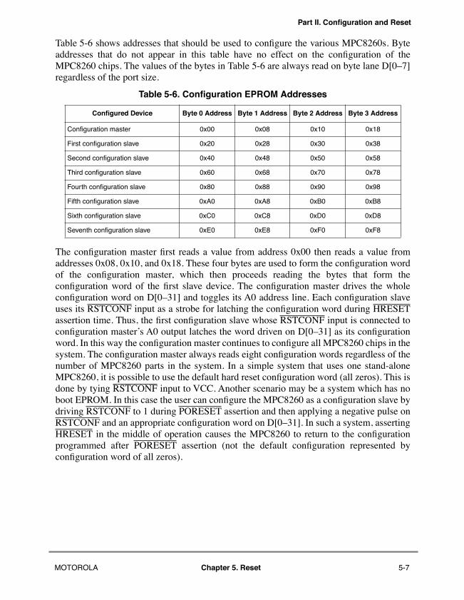
Part II. ConÞguration and Reset
Table 5-6 shows addresses that should be used to conÞgure the various MPC8260s. Byteaddresses that do not appear in this table have no effect on the conÞguration of theMPC8260 chips. The values of the bytes in Table 5-6 are always read on byte lane D[0Ð7]regardless of the port size.
The conÞguration master Þrst reads a value from address 0x00 then reads a value fromaddresses 0x08, 0x10, and 0x18. These four bytes are used to form the conÞguration wordof the conÞguration master, which then proceeds reading the bytes that form theconÞguration word of the Þrst slave device. The conÞguration master drives the wholeconÞguration word on D[0Ð31] and toggles its A0 address line. Each conÞguration slaveuses its RSTCONF input as a strobe for latching the conÞguration word during HRESETassertion time. Thus, the Þrst conÞguration slave whose RSTCONF input is connected toconÞguration masterÕs A0 output latches the word driven on D[0Ð31] as its conÞgurationword. In this way the conÞguration master continues to conÞgure all MPC8260 chips in thesystem. The conÞguration master always reads eight conÞguration words regardless of thenumber of MPC8260 parts in the system. In a simple system that uses one stand-aloneMPC8260, it is possible to use the default hard reset conÞguration word (all zeros). This isdone by tying RSTCONF input to VCC. Another scenario may be a system which has noboot EPROM. In this case the user can conÞgure the MPC8260 as a conÞguration slave bydriving RSTCONF to 1 during PORESET assertion and then applying a negative pulse onRSTCONF and an appropriate conÞguration word on D[0Ð31]. In such a system, assertingHRESET in the middle of operation causes the MPC8260 to return to the conÞgurationprogrammed after PORESET assertion (not the default conÞguration represented byconÞguration word of all zeros).
Table 5-6. Configuration EPROM Addresses
ConÞgured Device Byte 0 Address Byte 1 Address Byte 2 Address Byte 3 Address
ConÞguration master 0x00 0x08 0x10 0x18
First conÞguration slave 0x20 0x28 0x30 0x38
Second conÞguration slave 0x40 0x48 0x50 0x58
Third conÞguration slave 0x60 0x68 0x70 0x78
Fourth conÞguration slave 0x80 0x88 0x90 0x98
Fifth conÞguration slave 0xA0 0xA8 0xB0 0xB8
Sixth conÞguration slave 0xC0 0xC8 0xD0 0xD8
Seventh conÞguration slave 0xE0 0xE8 0xF0 0xF8
MOTOROLA Chapter 5. Reset 5-7
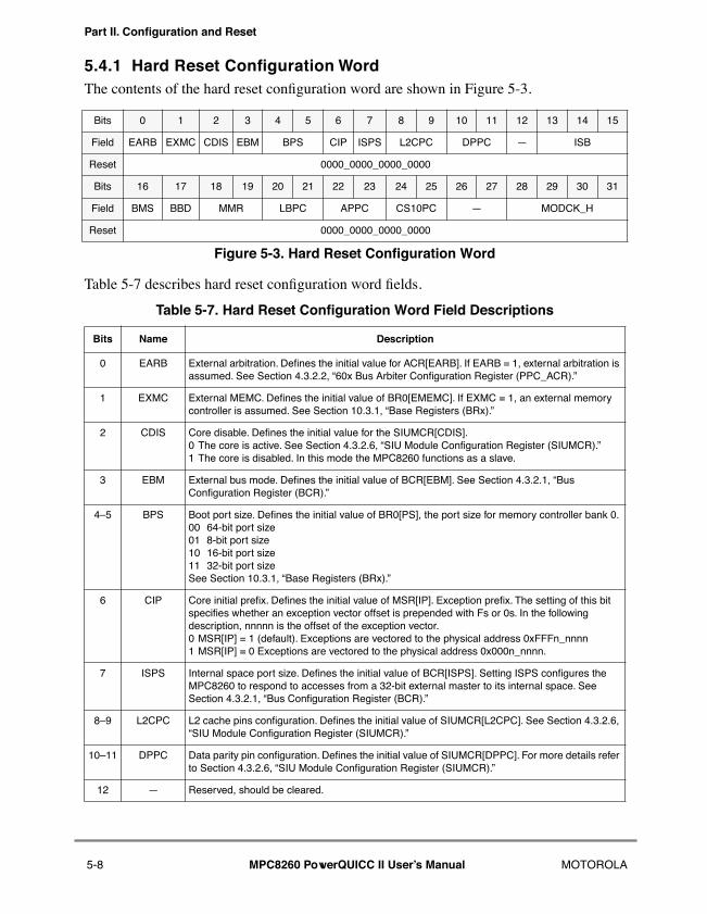
Part II. ConÞguration and Reset
5.4.1 Hard Reset ConÞguration WordThe contents of the hard reset conÞguration word are shown in Figure 5-3.
Table 5-7 describes hard reset conÞguration word Þelds.
Bits 0 1 2 3 4 5 6 7 8 9 10 11 12 13 14 15
Field EARB EXMC CDIS EBM BPS CIP ISPS L2CPC DPPC Ñ ISB
Reset 0000_0000_0000_0000
Bits 16 17 18 19 20 21 22 23 24 25 26 27 28 29 30 31
Field BMS BBD MMR LBPC APPC CS10PC Ñ MODCK_H
Reset 0000_0000_0000_0000
Figure 5-3. Hard Reset Configuration Word
Table 5-7. Hard Reset Configuration Word Field Descriptions
Bits Name Description
0 EARB External arbitration. DeÞnes the initial value for ACR[EARB]. If EARB = 1, external arbitration is assumed. See Section 4.3.2.2, Ò60x Bus Arbiter ConÞguration Register (PPC_ACR).Ó
1 EXMC External MEMC. DeÞnes the initial value of BR0[EMEMC]. If EXMC = 1, an external memory controller is assumed. See Section 10.3.1, ÒBase Registers (BRx).Ó
2 CDIS Core disable. DeÞnes the initial value for the SIUMCR[CDIS]. 0 The core is active. See Section 4.3.2.6, ÒSIU Module ConÞguration Register (SIUMCR).Ó1 The core is disabled. In this mode the MPC8260 functions as a slave.
3 EBM External bus mode. DeÞnes the initial value of BCR[EBM]. See Section 4.3.2.1, ÒBus ConÞguration Register (BCR).Ó
4Ð5 BPS Boot port size. DeÞnes the initial value of BR0[PS], the port size for memory controller bank 0. 00 64-bit port size01 8-bit port size10 16-bit port size11 32-bit port sizeSee Section 10.3.1, ÒBase Registers (BRx).Ó
6 CIP Core initial preÞx. DeÞnes the initial value of MSR[IP]. Exception preÞx. The setting of this bit speciÞes whether an exception vector offset is prepended with Fs or 0s. In the following description, nnnnn is the offset of the exception vector. 0 MSR[IP] = 1 (default). Exceptions are vectored to the physical address 0xFFFn_nnnn1 MSR[IP] = 0 Exceptions are vectored to the physical address 0x000n_nnnn.
7 ISPS Internal space port size. DeÞnes the initial value of BCR[ISPS]. Setting ISPS conÞgures the MPC8260 to respond to accesses from a 32-bit external master to its internal space. See Section 4.3.2.1, ÒBus ConÞguration Register (BCR).Ó
8Ð9 L2CPC L2 cache pins conÞguration. DeÞnes the initial value of SIUMCR[L2CPC]. See Section 4.3.2.6, ÒSIU Module ConÞguration Register (SIUMCR).Ó
10Ð11 DPPC Data parity pin conÞguration. DeÞnes the initial value of SIUMCR[DPPC]. For more details refer to Section 4.3.2.6, ÒSIU Module ConÞguration Register (SIUMCR).Ó
12 Ñ Reserved, should be cleared.
5-8 MPC8260 PowerQUICC II UserÕs Manual MOTOROLA
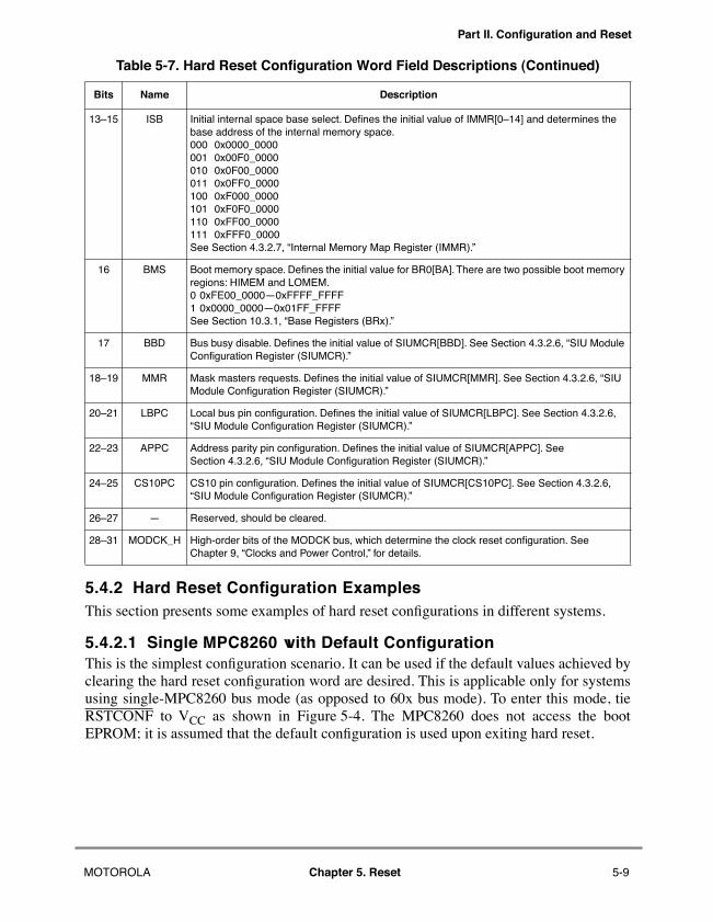
Part II. ConÞguration and Reset
5.4.2 Hard Reset ConÞguration ExamplesThis section presents some examples of hard reset conÞgurations in different systems.
5.4.2.1 Single MPC8260 with Default ConÞgurationThis is the simplest conÞguration scenario. It can be used if the default values achieved byclearing the hard reset conÞguration word are desired. This is applicable only for systemsusing single-MPC8260 bus mode (as opposed to 60x bus mode). To enter this mode, tieRSTCONF to VCC as shown in Figure 5-4. The MPC8260 does not access the bootEPROM; it is assumed that the default conÞguration is used upon exiting hard reset.
13Ð15 ISB Initial internal space base select. DeÞnes the initial value of IMMR[0Ð14] and determines the base address of the internal memory space. 000 0x0000_0000001 0x00F0_0000010 0x0F00_0000011 0x0FF0_0000100 0xF000_0000101 0xF0F0_0000110 0xFF00_0000111 0xFFF0_0000See Section 4.3.2.7, ÒInternal Memory Map Register (IMMR).Ó
16 BMS Boot memory space. DeÞnes the initial value for BR0[BA]. There are two possible boot memory regions: HIMEM and LOMEM. 0 0xFE00_0000Ñ0xFFFF_FFFF1 0x0000_0000Ñ0x01FF_FFFFSee Section 10.3.1, ÒBase Registers (BRx).Ó
17 BBD Bus busy disable. DeÞnes the initial value of SIUMCR[BBD]. See Section 4.3.2.6, ÒSIU Module ConÞguration Register (SIUMCR).Ó
18Ð19 MMR Mask masters requests. DeÞnes the initial value of SIUMCR[MMR]. See Section 4.3.2.6, ÒSIU Module ConÞguration Register (SIUMCR).Ó
20Ð21 LBPC Local bus pin conÞguration. DeÞnes the initial value of SIUMCR[LBPC]. See Section 4.3.2.6, ÒSIU Module ConÞguration Register (SIUMCR).Ó
22Ð23 APPC Address parity pin conÞguration. DeÞnes the initial value of SIUMCR[APPC]. See Section 4.3.2.6, ÒSIU Module ConÞguration Register (SIUMCR).Ó
24Ð25 CS10PC CS10 pin conÞguration. DeÞnes the initial value of SIUMCR[CS10PC]. See Section 4.3.2.6, ÒSIU Module ConÞguration Register (SIUMCR).Ó
26Ð27 Ñ Reserved, should be cleared.
28Ð31 MODCK_H High-order bits of the MODCK bus, which determine the clock reset conÞguration. See Chapter 9, ÒClocks and Power Control,Ó for details.
Table 5-7. Hard Reset Configuration Word Field Descriptions (Continued)
Bits Name Description
MOTOROLA Chapter 5. Reset 5-9
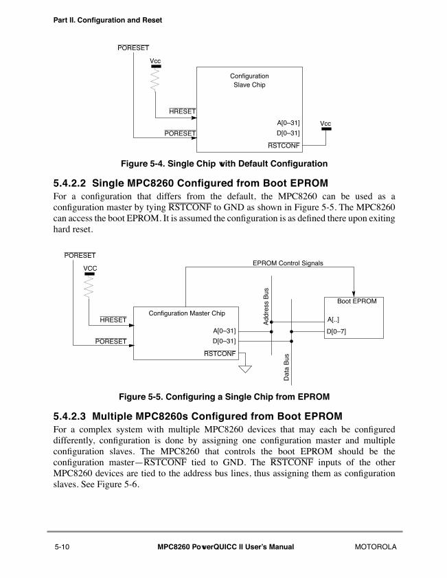
Part II. ConÞguration and Reset
Figure 5-4. Single Chip with Default Configuration
5.4.2.2 Single MPC8260 ConÞgured from Boot EPROMFor a conÞguration that differs from the default, the MPC8260 can be used as aconÞguration master by tying RSTCONF to GND as shown in Figure 5-5. The MPC8260can access the boot EPROM. It is assumed the conÞguration is as deÞned there upon exitinghard reset.
Figure 5-5. Configuring a Single Chip from EPROM
5.4.2.3 Multiple MPC8260s ConÞgured from Boot EPROMFor a complex system with multiple MPC8260 devices that may each be conÞgureddifferently, conÞguration is done by assigning one conÞguration master and multipleconÞguration slaves. The MPC8260 that controls the boot EPROM should be theconÞguration masterÑRSTCONF tied to GND. The RSTCONF inputs of the otherMPC8260 devices are tied to the address bus lines, thus assigning them as conÞgurationslaves. See Figure 5-6.
ConfigurationSlave Chip
PORESET
PORESET
RSTCONF
D[0Ð31]
A[0Ð31]
HRESET
Vcc
Vcc
Configuration Master Chip
PORESET
PORESET
Boot EPROM
EPROM Control Signals
RSTCONF
D[0Ð31]
D[0Ð7]A[0Ð31]
A[..]HRESET
VCCA
ddre
ss B
us
Dat
a B
us
5-10 MPC8260 PowerQUICC II UserÕs Manual MOTOROLA
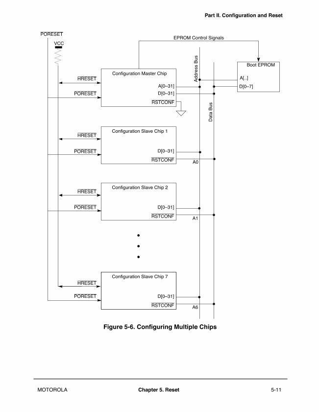
Part II. ConÞguration and Reset
Figure 5-6. Configuring Multiple Chips
PORESET
PORESET
PORESET
PORESET
A0
A1
A6
HRESET
HRESET
HRESET
HRESET
VCC
Configuration Master Chip
PORESET
Boot EPROM
EPROM Control Signals
RSTCONF
D[0Ð31]
D[0Ð7]A[0Ð31]
A[..]Add
ress
Bus
Dat
a B
us
Configuration Slave Chip 1
RSTCONF
D[0Ð31]
Configuration Slave Chip 2
RSTCONF
D[0Ð31]
Configuration Slave Chip 7
RSTCONF
D[0Ð31]
MOTOROLA Chapter 5. Reset 5-11
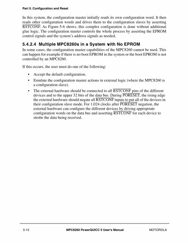
Part II. ConÞguration and Reset
In this system, the conÞguration master initially reads its own conÞguration word. It thenreads other conÞguration words and drives them to the conÞguration slaves by assertingRSTCONF. As Figure 5-6 shows, this complex conÞguration is done without additionalglue logic. The conÞguration master controls the whole process by asserting the EPROMcontrol signals and the systemÕs address signals as needed.
5.4.2.4 Multiple MPC8260s in a System with No EPROMIn some cases, the conÞguration master capabilities of the MPC8260 cannot be used. Thiscan happen for example if there is no boot EPROM in the system or the boot EPROM is notcontrolled by an MPC8260.
If this occurs, the user must do one of the following:
¥ Accept the default conÞguration,
¥ Emulate the conÞguration master actions in external logic (where the MPC8260 is a conÞguration slave).
¥ The external hardware should be connected to all RSTCONF pins of the different devices and to the upper 32 bits of the data bus. During PORESET, the rising edge the external hardware should negate all RSTCONF inputs to put all of the devices in their conÞguration slave mode. For 1,024 clocks after PORESET negation, the external hardware can conÞgure the different devices by driving appropriate conÞguration words on the data bus and asserting RSTCONF for each device to strobe the data being received.
5-12 MPC8260 PowerQUICC II UserÕs Manual MOTOROLA
Part IIIThe Hardware Interface
Intended AudiencePart III is intended for system designers who need to understand how each MPC8260 signalworks and how those signals interact.
ContentsPart III describes external signals, clocking, memory control, and power management ofthe MPC8260.
It contains the following chapters:
¥ Chapter 6, ÒExternal Signals,Ó shows a functional pinout of the MPC8260 and describes the MPC8260 signals.
¥ Chapter 7, Ò60x Signals,Ó describes signals on the 60x bus.
¥ Chapter 8, ÒThe 60x Bus,Ó describes the operation of the bus used by PowerPC processors.
¥ Chapter 9, ÒClocks and Power Control,Ó describes the clocking architecture of the MPC8260.
¥ Chapter 10, ÒMemory Controller,Ó describes the memory controller, which controlling a maximum of eight memory banks shared between a general-purpose chip-select machine (GPCM) and three user-programmable machines (UPMs).
¥ Chapter 11, ÒSecondary (L2) Cache Support,Ó provides information about implementation and conÞguration of a level-2 cache.
¥ Chapter 12, ÒIEEE 1149.1 Test Access Port,Ó describes the dedicated user-accessible test access port (TAP), which is fully compatible with the IEEE 1149.1 Standard Test Access Port and Boundary Scan Architecture.
MOTOROLA Part III. The Hardware Interface Part III-i
Part III. The Hardware Interface
Suggested ReadingThis section lists additional reading that provides background for the information in thismanual as well as general information about the PowerPC architecture.
MPC8xx DocumentationSupporting documentation for the MPC8260 can be accessed through the world-wide webat http://www.motorola.com/SPS/RISC/netcomm. This documentation includes technicalspeciÞcations, reference materials, and detailed applications notes.
PowerPC DocumentationThe PowerPC documentation is organized in the following types of documents:
¥ PowerPC Microprocessor Family: The Bus Interface for 32-Bit Microprocessors (Motorola order #: MPCBUSIF/AD) provides a detailed functional description of the 60x bus interface, as implemented on the PowerPC MPC601ª, MPC603, MPC604, and MPC750 family of PowerPC microprocessors. This document is intended to help system and chip set developers by providing a centralized reference source to identify the bus interface presented by the 60x family of PowerPC microprocessors.
¥ Application notesÑThese short documents contain useful information about speciÞc design issues useful to programmers and engineers working with PowerPC processors.
For a current list of PowerPC documentation, refer to the world-wide web at http://www.mot.com/PowerPC.
ConventionsThis document uses the following notational conventions:
Bold entries in Þgures and tables showing registers and parameter RAM should be initialized by the user.
mnemonics Instruction mnemonics are shown in lowercase bold.
italics Italics indicate variable command parameters, for example, bcctrx.Book titles in text are set in italics.
0x0 PreÞx to denote hexadecimal number
0b0 PreÞx to denote binary number
REG[FIELD] Abbreviations or acronyms for registers or buffer descriptors are shown in uppercase text. SpeciÞc bits, Þelds, or numerical ranges appear in brackets. For example, MSR[LE] refers to the little-endian mode enable bit in the machine state register.
x In certain contexts, such as in a signal encoding or a bit Þeld, indicates a donÕt care.
Bold
Part III-ii MPC8260 PowerQUICC II UserÕs Manual MOTOROLA
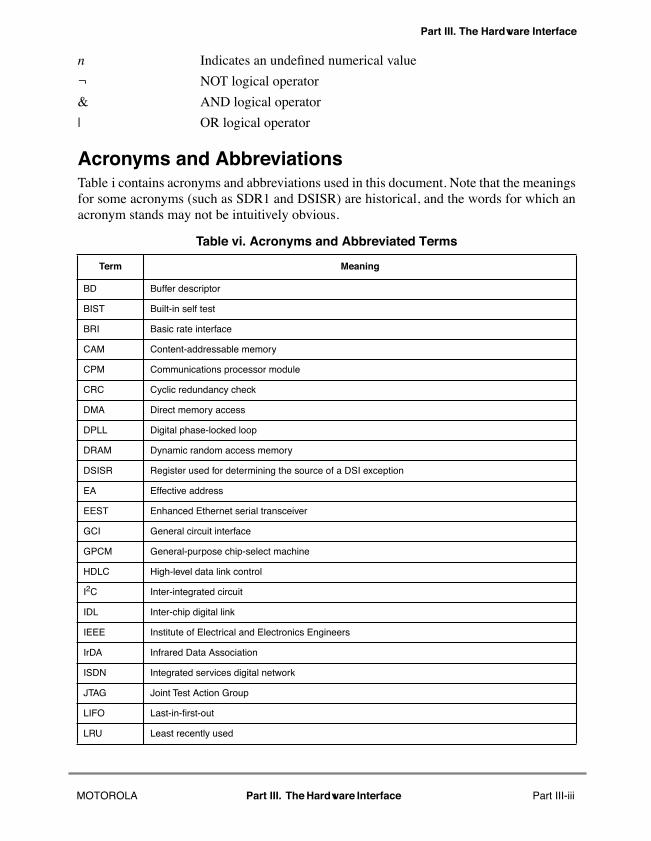
Part III. The Hardware Interface
n Indicates an undeÞned numerical value
 NOT logical operator
& AND logical operator
| OR logical operator
Acronyms and AbbreviationsTable i contains acronyms and abbreviations used in this document. Note that the meaningsfor some acronyms (such as SDR1 and DSISR) are historical, and the words for which anacronym stands may not be intuitively obvious.
Table vi. Acronyms and Abbreviated Terms
Term Meaning
BD Buffer descriptor
BIST Built-in self test
BRI Basic rate interface
CAM Content-addressable memory
CPM Communications processor module
CRC Cyclic redundancy check
DMA Direct memory access
DPLL Digital phase-locked loop
DRAM Dynamic random access memory
DSISR Register used for determining the source of a DSI exception
EA Effective address
EEST Enhanced Ethernet serial transceiver
GCI General circuit interface
GPCM General-purpose chip-select machine
HDLC High-level data link control
I2C Inter-integrated circuit
IDL Inter-chip digital link
IEEE Institute of Electrical and Electronics Engineers
IrDA Infrared Data Association
ISDN Integrated services digital network
JTAG Joint Test Action Group
LIFO Last-in-Þrst-out
LRU Least recently used
MOTOROLA Part III. The Hardware Interface Part III-iii
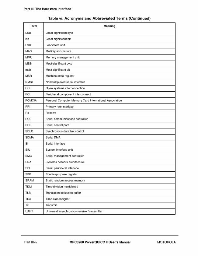
Part III. The Hardware Interface
LSB Least-signiÞcant byte
lsb Least-signiÞcant bit
LSU Load/store unit
MAC Multiply accumulate
MMU Memory management unit
MSB Most-signiÞcant byte
msb Most-signiÞcant bit
MSR Machine state register
NMSI Nonmultiplexed serial interface
OSI Open systems interconnection
PCI Peripheral component interconnect
PCMCIA Personal Computer Memory Card International Association
PRI Primary rate interface
Rx Receive
SCC Serial communications controller
SCP Serial control port
SDLC Synchronous data link control
SDMA Serial DMA
SI Serial interface
SIU System interface unit
SMC Serial management controller
SNA Systems network architecture.
SPI Serial peripheral interface
SPR Special-purpose register
SRAM Static random access memory
TDM Time-division multiplexed
TLB Translation lookaside buffer
TSA Time-slot assigner
Tx Transmit
UART Universal asynchronous receiver/transmitter
Table vi. Acronyms and Abbreviated Terms (Continued)
Term Meaning
Part III-iv MPC8260 PowerQUICC II UserÕs Manual MOTOROLA
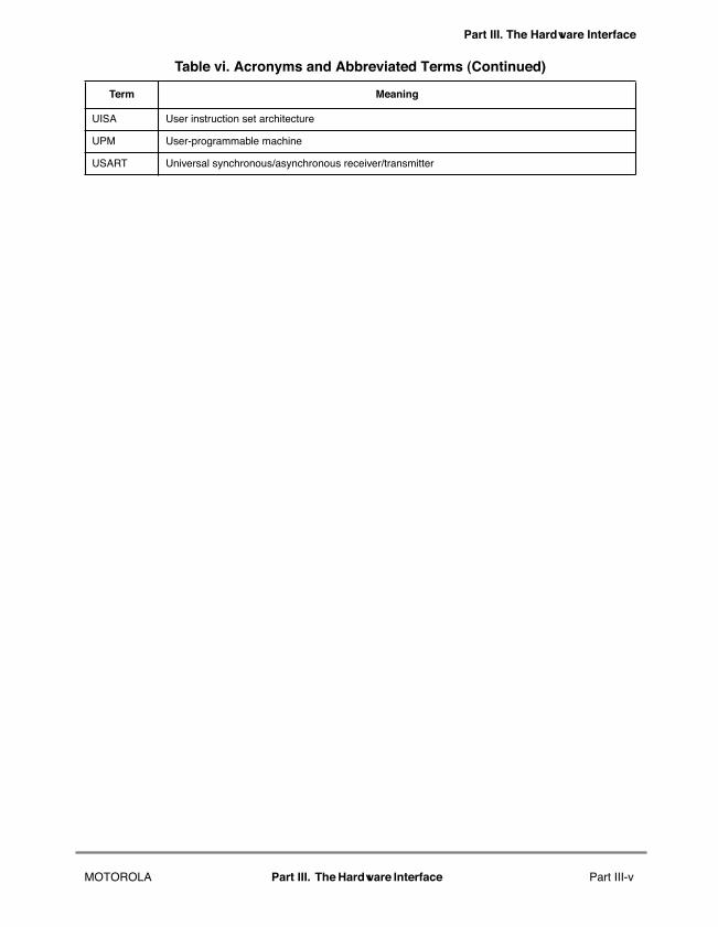
Part III. The Hardware Interface
UISA User instruction set architecture
UPM User-programmable machine
USART Universal synchronous/asynchronous receiver/transmitter
Table vi. Acronyms and Abbreviated Terms (Continued)
Term Meaning
MOTOROLA Part III. The Hardware Interface Part III-v

Part III. The Hardware Interface
Part III-vi MPC8260 PowerQUICC II UserÕs Manual MOTOROLA
Chapter 6 External Signals6060
This chapter describes the MPC8260 external signals. A more detailed description of 60xbus signals is provided in Chapter 8, ÒThe 60x Bus.Ó
6.1 Functional PinoutFigure 6-1 shows MPC8260 signals grouped by function. Note that many of these signalsare multiplexed and this Þgure does not indicate how these signals are multiplexed.
NOTEA bar over a signal name indicates that the signal is activelowÑfor example, BB (bus busy). Active-low signals arereferred to as asserted (active) when they are low and negatedwhen they are high. Signals that are not active low, such asTSIZ[0Ð1] (transfer size signals) are referred to as assertedwhen they are high and negated when they are low.
MOTOROLA Chapter 6. External Signals 6-1
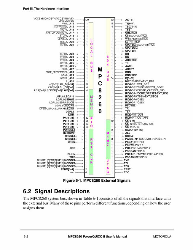
Part III. The Hardware Interface
Figure 6-1. MPC8260 External Signals
6.2 Signal DescriptionsThe MPC8260 system bus, shown in Table 6-1, consists of all the signals that interface withthe external bus. Many of these pins perform different functions, depending on how the userassigns them.
VCCSYN/GNDSYN/VCCSYN1//VD-DH/VDD/VSS ¾¾¾>100
MPC8260
60x
BUS
32 <¾¾> A[0Ð31]
PAR/L_A14 <¾¾> 1
LOCAL
BUS
5 <¾¾> TT[0Ð4]SMI/FRAME/L_A15 <¾¾> 1 4 <¾¾> TSIZ[0Ð3]
TRDY/L_A16 <¾¾> 1 1 <¾¾> TBSTCKSTOP_OUT/IRDY/L_A17 <¾¾> 1 1 <¾¾> GBL/IRQ1
STOP/L_A18 <¾¾> 1 1 <¾¾> CI/BADDR29/IRQ2DEVSEL/L_A19 <¾¾> 1 1 <¾¾> WT/BADDR30/IRQ3
IDSEL/L_A20 <¾¾> 1 1 <¾¾¾ L2_HIT/IRQ4PERR/L_A21 <¾¾> 1 1 <¾¾> CPU_BG/BADDR31/IRQ5
1 ¾¾¾> CPU_DBG1 ¾¾¾> CPU_BR
SERR/L_A22 <¾¾> 1 1 <¾¾> BRREQ0/L_A23 <¾¾> 1 1 <¾¾> BGREQ1/L_A24 <¾¾> 1 1 <¾¾> ABB/IRQ2GNT0/L_A25 <¾¾> 1 1 <¾¾> TSGNT1/L_A26 <¾¾¾ 1 1 <¾¾> AACK
CLK/L_A27 <¾¾> 1 1 <¾¾> ARTRYCORE_SRESET/RST/L_A28 <¾¾> 1 1 <¾¾> DBG
INTA/L_A29 <¾¾> 1 1 <¾¾> DBB/IRQ3LOCK/L_A30 <¾¾> 1 64 <¾¾> D[0Ð63]
L_A31 <¾¾> 1 1 <¾¾> NC/DP0/RSRV/EXT_BR2AD[0–31]/LCL_D[0Ð31] <¾¾> 32 1 <¾¾> IRQ1/DP1/EXT_BG2
C/BE[0–3]/LCL_DP[0Ð3] <¾¾> 4 1 <¾¾> IRQ2/DP2/TLBISYNC/EXT_DBG2LBS[0Ð3]/LSDDQM[0Ð3]/LWE[0Ð3] <¾¾¾ 4
MEMC
1 <¾¾> IRQ3/DP3/CKSTP_OUT/EXT_BR31 <¾¾> IRQ4/DP4/CORE_SRESET/EXT_BG3
LGPL0/LSDA10 <¾¾¾ 1 1 <¾¾> IRQ5/DP5/TBEN/EXT_DBG3LGPL1/LSDWE <¾¾¾ 1 1 <¾¾> IRQ6/DP6/CSE0
LGPL2/LSDRAS/LOE <¾¾¾ 1 1 <¾¾> IRQ7/DP7/CSE1LGPL3/LSDCAS <¾¾¾ 1 1 <¾¾> PSDVAL
LPBS/LGPL4/LUPWAIT/LGTA <¾¾> 1 1 <¾¾> TALGPL5 <¾¾> 1 1 <¾¾> TEA
LWR <¾¾> 1 1 <¾¾> IRQ0/NMI_OUTPA[0Ð31] <¾¾> 32 P
IO
1 <¾¾> IRQ7/INT_OUT/APEPB[4Ð31] <¾¾> 28
MEMC
10 ¾¾¾> CS[0Ð9]PC[0Ð31] <¾¾> 32 1 <¾¾> CS[10]/BCTL1/DBG_DISPD[4Ð31] <¾¾> 28 1 <¾¾> CS[11]/AP[0]PORESET¾¾¾> 1
RST
CLK
2 ¾¾¾> BADDR[27Ð28]RSTCONF¾¾¾> 1 1 ¾¾¾> ALE
HRESET<¾¾> 1 1 ¾¾¾> BCTL0SRESET<¾¾> 1 8 ¾¾¾> PWE[0Ð7]/PSDDQM[0Ð7]/PBS[0Ð7]
QREQ<¾¾¾ 1 1 ¾¾¾> PSDA10/PGPL01 ¾¾¾> PSDWE/PGPL1
XFC¾¾¾> 1 1 ¾¾¾> POE/PSDRAS/PGPL21 ¾¾¾> PSDCAS/PGPL3
CLKIN¾¾¾> 1 1 <¾¾> PGTA/PUPMWAIT/PGPL4/PPBSTRIS¾¾¾> 1 1 ¾¾¾> PSDAMUX/PGPL5
BNKSEL[0]/TC[0]/AP[1]/MODCK1<¾¾> 1 JTAG
1 <¾¾- TMSBNKSEL[1]/TC[1]/AP[2]/MODCK2<¾¾> 1 1 <¾¾¾TDIBNKSEL[2]/TC[2]/AP[3]/MODCK3<¾¾> 1 1 <¾¾- TCK
TERM[0Ð1] ¾¾¾> 2 1 <¾¾- TRSTNC ¾¾¾> 4 1 -¾¾> TDO
6-2 MPC8260 PowerQUICC II UserÕs Manual MOTOROLA
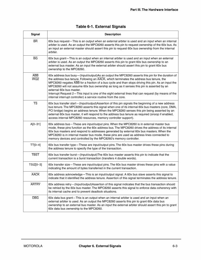
Part III. The Hardware Interface
Table 6-1. External Signals
Signal Description
BR 60x bus requestÑThis is an output when an external arbiter is used and an input when an internal arbiter is used. As an output the MPC8260 asserts this pin to request ownership of the 60x bus. As an input an external master should assert this pin to request 60x bus ownership from the internal arbiter.
BG 60x bus grantÑThis is an output when an internal arbiter is used and an input when an external arbiter is used. As an output the MPC8260 asserts this pin to grant 60x bus ownership to an external bus master. As an input the external arbiter should assert this pin to grant 60x bus ownership to the MPC8260.
ABBIRQ2
60x address bus busyÑ(Input/output)As an output the MPC8260 asserts this pin for the duration of the address bus tenure. Following an AACK, which terminates the address bus tenure, the MPC8260 negates ABB for a fraction of a bus cycle and than stops driving this pin. As an input the MPC8260 will not assume 60x bus ownership as long as it senses this pin is asserted by an external 60x bus master.Interrupt Request 2ÑThis input is one of the eight external lines that can request (by means of the internal interrupt controller) a service routine from the core.
TS 60x bus transfer startÑ(Input/output)Assertion of this pin signals the beginning of a new address bus tenure. The MPC8260 asserts this signal when one of its internal 60x bus masters (core, DMA, PCI bridge) begins an address tenure. When the MPC8260 senses this pin being asserted by an external 60x bus master, it will respond to the address bus tenure as required (snoop if enabled, access internal MPC8260 resources, memory controller support).
A[0Ð31] 60x address busÑThese are input/output pins. When the MPC8260 is in external master bus mode, these pins function as the 60x address bus. The MPC8260 drives the address of its internal 60x bus masters and respond to addresses generated by external 60x bus masters. When the MPC8260 is in internal master bus mode, these pins are used as address lines connected to memory devices and controlled by the MPC8260Õs memory controller.
TT[0Ð4] 60x bus transfer typeÑThese are input/output pins. The 60x bus master drives these pins during the address tenure to specify the type of the transaction.
TBST 60x bus transfer burstÑ(Input/output)The 60x bus master asserts this pin to indicate that the current transaction is a burst transaction (transfers 4 double words).
TSIZ[0Ð3] 60x transfer sizeÑThese are input/output pins. The 60x bus master drives these pins with a value indicating the amount of bytes transferred in the current transaction.
AACK 60x address acknowledgeÑThis is an input/output signal. A 60x bus slave asserts this signal to indicate that it identiÞed the address tenure. Assertion of this signal terminates the address tenure.
ARTRY 60x address retryÑ(Input/output)Assertion of this signal indicates that the bus transaction should be retried by the 60x bus master. The MPC8260 asserts this signal to enforce data coherency with its internal cache and to prevent deadlock situations.
DBG 60x data bus grantÑThis is an output when an internal arbiter is used and an input when an external arbiter is used. As an output the MPC8260 asserts this pin to grant 60x data bus ownership to an external bus master. As an input the external arbiter should assert this pin to grant 60x data bus ownership to the MPC8260.
MOTOROLA Chapter 6. External Signals 6-3
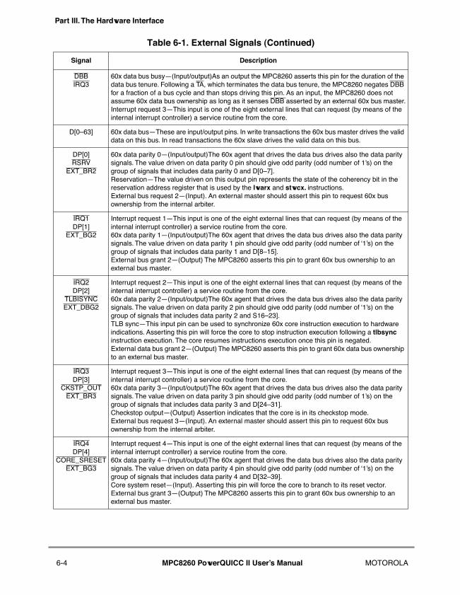
Part III. The Hardware Interface
DBBIRQ3
60x data bus busyÑ(Input/output)As an output the MPC8260 asserts this pin for the duration of the data bus tenure. Following a TA, which terminates the data bus tenure, the MPC8260 negates DBB for a fraction of a bus cycle and than stops driving this pin. As an input, the MPC8260 does not assume 60x data bus ownership as long as it senses DBB asserted by an external 60x bus master.Interrupt request 3ÑThis input is one of the eight external lines that can request (by means of the internal interrupt controller) a service routine from the core.
D[0Ð63] 60x data busÑThese are input/output pins. In write transactions the 60x bus master drives the valid data on this bus. In read transactions the 60x slave drives the valid data on this bus.
DP[0]RSRV
EXT_BR2
60x data parity 0Ñ(Input/output)The 60x agent that drives the data bus drives also the data parity signals. The value driven on data parity 0 pin should give odd parity (odd number of 1Õs) on the group of signals that includes data parity 0 and D[0Ð7].ReservationÑThe value driven on this output pin represents the state of the coherency bit in the reservation address register that is used by the lwarx and stwcx. instructions.External bus request 2Ñ(Input). An external master should assert this pin to request 60x bus ownership from the internal arbiter.
IRQ1DP[1]
EXT_BG2
Interrupt request 1ÑThis input is one of the eight external lines that can request (by means of the internal interrupt controller) a service routine from the core.60x data parity 1Ñ(Input/output)The 60x agent that drives the data bus drives also the data parity signals. The value driven on data parity 1 pin should give odd parity (odd number of Ô1Õs) on the group of signals that includes data parity 1 and D[8Ð15].External bus grant 2Ñ(Output) The MPC8260 asserts this pin to grant 60x bus ownership to an external bus master.
IRQ2DP[2]
TLBISYNCEXT_DBG2
Interrupt request 2ÑThis input is one of the eight external lines that can request (by means of the internal interrupt controller) a service routine from the core.60x data parity 2Ñ(Input/output)The 60x agent that drives the data bus drives also the data parity signals. The value driven on data parity 2 pin should give odd parity (odd number of Ô1Õs) on the group of signals that includes data parity 2 and S16Ð23].TLB syncÑThis input pin can be used to synchronize 60x core instruction execution to hardware indications. Asserting this pin will force the core to stop instruction execution following a tlbsync instruction execution. The core resumes instructions execution once this pin is negated.External data bus grant 2Ñ(Output) The MPC8260 asserts this pin to grant 60x data bus ownership to an external bus master.
IRQ3DP[3]
CKSTP_OUTEXT_BR3
Interrupt request 3ÑThis input is one of the eight external lines that can request (by means of the internal interrupt controller) a service routine from the core.60x data parity 3Ñ(Input/output)The 60x agent that drives the data bus drives also the data parity signals. The value driven on data parity 3 pin should give odd parity (odd number of 1Õs) on the group of signals that includes data parity 3 and D[24Ð31].Checkstop outputÑ(Output) Assertion indicates that the core is in its checkstop mode.External bus request 3Ñ(Input). An external master should assert this pin to request 60x bus ownership from the internal arbiter.
IRQ4DP[4]
CORE_SRESETEXT_BG3
Interrupt request 4ÑThis input is one of the eight external lines that can request (by means of the internal interrupt controller) a service routine from the core.60x data parity 4Ñ(Input/output)The 60x agent that drives the data bus drives also the data parity signals. The value driven on data parity 4 pin should give odd parity (odd number of Ô1Õs) on the group of signals that includes data parity 4 and D[32Ð39].Core system resetÑ(Input). Asserting this pin will force the core to branch to its reset vector.External bus grant 3Ñ(Output) The MPC8260 asserts this pin to grant 60x bus ownership to an external bus master.
Table 6-1. External Signals (Continued)
Signal Description
6-4 MPC8260 PowerQUICC II UserÕs Manual MOTOROLA
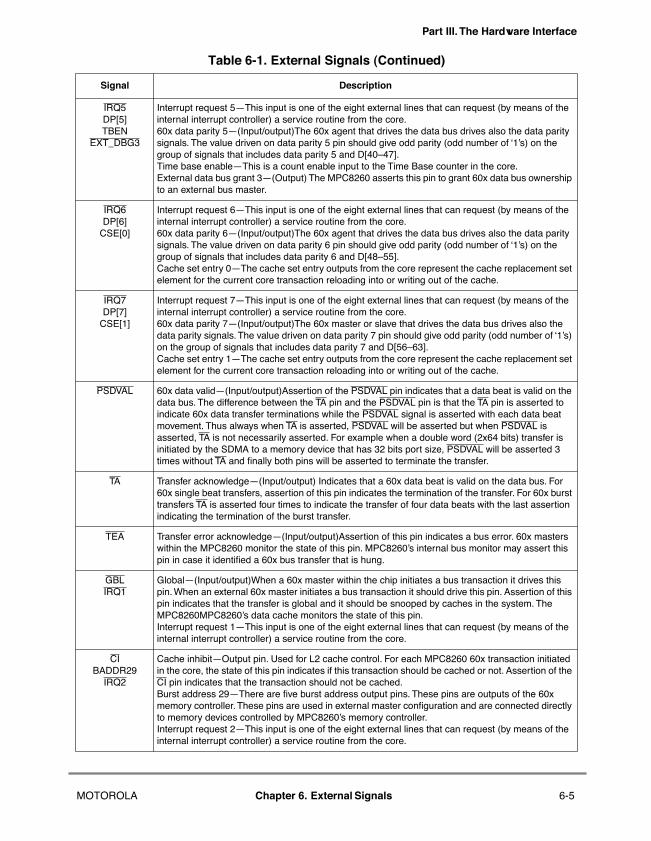
Part III. The Hardware Interface
IRQ5DP[5]TBEN
EXT_DBG3
Interrupt request 5ÑThis input is one of the eight external lines that can request (by means of the internal interrupt controller) a service routine from the core.60x data parity 5Ñ(Input/output)The 60x agent that drives the data bus drives also the data parity signals. The value driven on data parity 5 pin should give odd parity (odd number of Ô1Õs) on the group of signals that includes data parity 5 and D[40Ð47].Time base enableÑThis is a count enable input to the Time Base counter in the core.External data bus grant 3Ñ(Output) The MPC8260 asserts this pin to grant 60x data bus ownership to an external bus master.
IRQ6DP[6]
CSE[0]
Interrupt request 6ÑThis input is one of the eight external lines that can request (by means of the internal interrupt controller) a service routine from the core.60x data parity 6Ñ(Input/output)The 60x agent that drives the data bus drives also the data parity signals. The value driven on data parity 6 pin should give odd parity (odd number of Ô1Õs) on the group of signals that includes data parity 6 and D[48Ð55].Cache set entry 0ÑThe cache set entry outputs from the core represent the cache replacement set element for the current core transaction reloading into or writing out of the cache.
IRQ7DP[7]
CSE[1]
Interrupt request 7ÑThis input is one of the eight external lines that can request (by means of the internal interrupt controller) a service routine from the core.60x data parity 7Ñ(Input/output)The 60x master or slave that drives the data bus drives also the data parity signals. The value driven on data parity 7 pin should give odd parity (odd number of Ô1Õs) on the group of signals that includes data parity 7 and D[56Ð63].Cache set entry 1ÑThe cache set entry outputs from the core represent the cache replacement set element for the current core transaction reloading into or writing out of the cache.
PSDVAL 60x data validÑ(Input/output)Assertion of the PSDVAL pin indicates that a data beat is valid on the data bus. The difference between the TA pin and the PSDVAL pin is that the TA pin is asserted to indicate 60x data transfer terminations while the PSDVAL signal is asserted with each data beat movement. Thus always when TA is asserted, PSDVAL will be asserted but when PSDVAL is asserted, TA is not necessarily asserted. For example when a double word (2x64 bits) transfer is initiated by the SDMA to a memory device that has 32 bits port size, PSDVAL will be asserted 3 times without TA and Þnally both pins will be asserted to terminate the transfer.
TA Transfer acknowledgeÑ(Input/output) Indicates that a 60x data beat is valid on the data bus. For 60x single beat transfers, assertion of this pin indicates the termination of the transfer. For 60x burst transfers TA is asserted four times to indicate the transfer of four data beats with the last assertion indicating the termination of the burst transfer.
TEA Transfer error acknowledgeÑ(Input/output)Assertion of this pin indicates a bus error. 60x masters within the MPC8260 monitor the state of this pin. MPC8260Õs internal bus monitor may assert this pin in case it identiÞed a 60x bus transfer that is hung.
GBLIRQ1
GlobalÑ(Input/output)When a 60x master within the chip initiates a bus transaction it drives this pin. When an external 60x master initiates a bus transaction it should drive this pin. Assertion of this pin indicates that the transfer is global and it should be snooped by caches in the system. The MPC8260MPC8260Õs data cache monitors the state of this pin.Interrupt request 1ÑThis input is one of the eight external lines that can request (by means of the internal interrupt controller) a service routine from the core.
CIBADDR29
IRQ2
Cache inhibitÑOutput pin. Used for L2 cache control. For each MPC8260 60x transaction initiated in the core, the state of this pin indicates if this transaction should be cached or not. Assertion of the CI pin indicates that the transaction should not be cached. Burst address 29ÑThere are Þve burst address output pins. These pins are outputs of the 60x memory controller. These pins are used in external master conÞguration and are connected directly to memory devices controlled by MPC8260Õs memory controller.Interrupt request 2ÑThis input is one of the eight external lines that can request (by means of the internal interrupt controller) a service routine from the core.
Table 6-1. External Signals (Continued)
Signal Description
MOTOROLA Chapter 6. External Signals 6-5
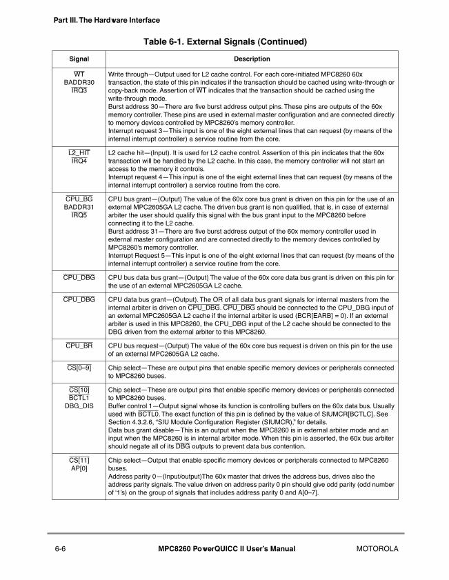
Part III. The Hardware Interface
WTBADDR30
IRQ3
Write throughÑOutput used for L2 cache control. For each core-initiated MPC8260 60x transaction, the state of this pin indicates if the transaction should be cached using write-through or copy-back mode. Assertion of WT indicates that the transaction should be cached using the write-through mode. Burst address 30ÑThere are Þve burst address output pins. These pins are outputs of the 60x memory controller. These pins are used in external master conÞguration and are connected directly to memory devices controlled by MPC8260Õs memory controller.Interrupt request 3ÑThis input is one of the eight external lines that can request (by means of the internal interrupt controller) a service routine from the core.
L2_HITIRQ4
L2 cache hitÑ(Input). It is used for L2 cache control. Assertion of this pin indicates that the 60x transaction will be handled by the L2 cache. In this case, the memory controller will not start an access to the memory it controls.Interrupt request 4ÑThis input is one of the eight external lines that can request (by means of the internal interrupt controller) a service routine from the core.
CPU_BGBADDR31
IRQ5
CPU bus grantÑ(Output) The value of the 60x core bus grant is driven on this pin for the use of an external MPC2605GA L2 cache. The driven bus grant is non qualiÞed, that is, in case of external arbiter the user should qualify this signal with the bus grant input to the MPC8260 before connecting it to the L2 cache.Burst address 31ÑThere are Þve burst address output of the 60x memory controller used in external master conÞguration and are connected directly to the memory devices controlled by MPC8260Õs memory controller.Interrupt Request 5ÑThis input is one of the eight external lines that can request (by means of the internal interrupt controller) a service routine from the core.
CPU_DBG CPU bus data bus grantÑ(Output) The value of the 60x core data bus grant is driven on this pin for the use of an external MPC2605GA L2 cache.
CPU_DBG CPU data bus grantÑ(Output). The OR of all data bus grant signals for internal masters from the internal arbiter is driven on CPU_DBG. CPU_DBG should be connected to the CPU_DBG input of an external MPC2605GA L2 cache if the internal arbiter is used (BCR[EARB] = 0). If an external arbiter is used in this MPC8260, the CPU_DBG input of the L2 cache should be connected to the DBG driven from the external arbiter to this MPC8260.
CPU_BR CPU bus requestÑ(Output) The value of the 60x core bus request is driven on this pin for the use of an external MPC2605GA L2 cache.
CS[0Ð9] Chip selectÑThese are output pins that enable speciÞc memory devices or peripherals connected to MPC8260 buses.
CS[10]BCTL1
DBG_DIS
Chip selectÑThese are output pins that enable speciÞc memory devices or peripherals connected to MPC8260 buses.Buffer control 1ÑOutput signal whose its function is controlling buffers on the 60x data bus. Usually used with BCTL0. The exact function of this pin is deÞned by the value of SIUMCR[BCTLC]. See Section 4.3.2.6, ÒSIU Module ConÞguration Register (SIUMCR),Ó for details.Data bus grant disableÑThis is an output when the MPC8260 is in external arbiter mode and an input when the MPC8260 is in internal arbiter mode. When this pin is asserted, the 60x bus arbiter should negate all of its DBG outputs to prevent data bus contention.
CS[11]AP[0]
Chip selectÑOutput that enable speciÞc memory devices or peripherals connected to MPC8260 buses.Address parity 0Ñ(Input/output)The 60x master that drives the address bus, drives also the address parity signals. The value driven on address parity 0 pin should give odd parity (odd number of Ô1Õs) on the group of signals that includes address parity 0 and A[0Ð7].
Table 6-1. External Signals (Continued)
Signal Description
6-6 MPC8260 PowerQUICC II UserÕs Manual MOTOROLA
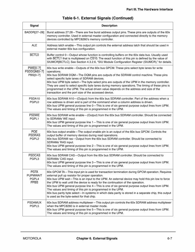
Part III. The Hardware Interface
BADDR[27Ð28] Burst address 27:28ÑThere are Þve burst address output pins. These pins are outputs of the 60x memory controller. Used in external master conÞguration and connected directly to the memory devices controlled by MPC8260Õs memory controller.
ALE Address latch enableÑThis output pin controls the external address latch that should be used in external master 60x bus conÞguration.
BCTL0 Buffer control 0ÑOutput whose function is controlling buffers on the 60x data bus. Usually used with BCTL1 that is multiplexed on CS10. The exact function of this pin is deÞned by the value of SIUMCR[BCTLC]. See Section 4.3.2.6, ÒSIU Module ConÞguration Register (SIUMCR),Ó for details.
PWE[0Ð7]PSDDQM[0Ð7]
PBS[0Ð7]
60x bus write enableÑOutputs of the 60x bus GPCM. These pins select byte lanes for write operations.60x bus SDRAM DQMÑThe DQM pins are outputs of the SDRAM control machine. These pins select speciÞc byte lanes of SDRAM devices.60x bus UPM byte selectÑThe byte select pins are outputs of the UPM in the memory controller. They are used to select speciÞc byte lanes during memory operations. The timing of these pins is programmed in the UPM. The actual driven value depends on the address and size of the transaction and the port size of the accessed device.
PSDA10PGPL0
60x bus SDRAM A10Ñ(Output) from the 60x bus SDRAM controller. Part of the address when a row address is driven and is part of the command when a column address is driven.60x bus UPM general purpose line 0ÑThis is one of six general purpose output lines from UPM. The values and timing of this pin is programmed in the UPM.
PSDWEPGPL1
60x bus SDRAM write enableÑ(Output) from the 60x bus SDRAM controller. Should be connected to SDRAMsÕ WE input.60x bus UPM general purpose line 1ÑThis is one of six general purpose output lines from UPM. The values and timing of this pin is programmed in the UPM.
POEPSDRASPGPL2
60x bus output enableÑThe output enable pin is an output of the 60x bus GPCM. Controls the output buffer of memory devices during read operations.60x bus SDRAM rasÑOutput from the 60x bus SDRAM controller. Should be connected to SDRAMsÕ RAS input.60x bus UPM general purpose line 2ÑThis is one of six general purpose output lines from UPM. The values and timing of this pin is programmed in the UPM.
PSDCASPGPL3
60x bus SDRAM CASÑOutput from the 60x bus SDRAM controller. Should be connected to SDRAMsÕ CAS input.60x bus UPM general purpose line 3ÑThis is one of six general purpose output lines from UPM. The values and timing of this pin is programmed in the UPM.
PGTAPUPMWAIT
PGPL4PPBS
60x GPCM TAÑThis input pin is used for transaction termination during GPCM operation. Requires external pull up resistor for proper operation.60x bus UPM waitÑThis is an input to the UPM. An external device may hold this pin low to force the UPM to wait until the device is ready for the continuation of the operation.60x bus UPM general purpose line 4ÑThis is one of six general purpose output lines from UPM. The values and timing of this pin is programmed in the UPM.60x bus parity byte selectÑIn systems in which data parity is stored in a separate chip, this output is used as the byte-select for that chip.
PSDAMUXPGPL5
60x bus SDRAM address multiplexerÑThis output pin controls the 60x SDRAM address multiplexer when the MPC8260 is in external master mode.60x bus UPM general purpose line 5ÑThis is one of six general purpose output lines from UPM. The values and timing of this pin is programmed in the UPM.
Table 6-1. External Signals (Continued)
Signal Description
MOTOROLA Chapter 6. External Signals 6-7
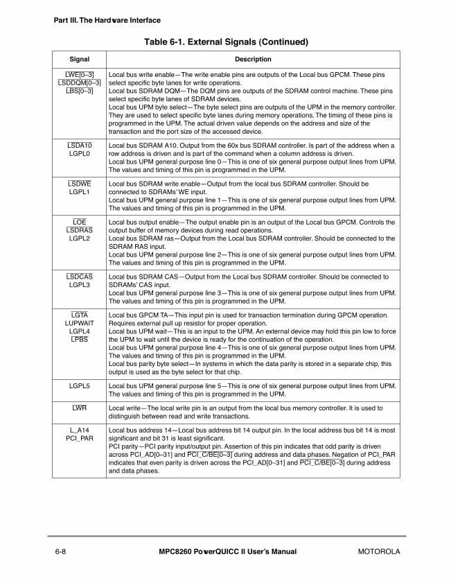
Part III. The Hardware Interface
LWE[0Ð3]LSDDQM[0Ð3]
LBS[0Ð3]
Local bus write enableÑThe write enable pins are outputs of the Local bus GPCM. These pins select speciÞc byte lanes for write operations.Local bus SDRAM DQMÑThe DQM pins are outputs of the SDRAM control machine. These pins select speciÞc byte lanes of SDRAM devices.Local bus UPM byte selectÑThe byte select pins are outputs of the UPM in the memory controller. They are used to select speciÞc byte lanes during memory operations. The timing of these pins is programmed in the UPM. The actual driven value depends on the address and size of the transaction and the port size of the accessed device.
LSDA10LGPL0
Local bus SDRAM A10. Output from the 60x bus SDRAM controller. Is part of the address when a row address is driven and is part of the command when a column address is driven.Local bus UPM general purpose line 0ÑThis is one of six general purpose output lines from UPM. The values and timing of this pin is programmed in the UPM.
LSDWELGPL1
Local bus SDRAM write enableÑOutput from the local bus SDRAM controller. Should be connected to SDRAMsÕ WE input.Local bus UPM general purpose line 1ÑThis is one of six general purpose output lines from UPM. The values and timing of this pin is programmed in the UPM.
LOELSDRASLGPL2
Local bus output enableÑThe output enable pin is an output of the Local bus GPCM. Controls the output buffer of memory devices during read operations.Local bus SDRAM rasÑOutput from the Local bus SDRAM controller. Should be connected to the SDRAM RAS input.Local bus UPM general purpose line 2ÑThis is one of six general purpose output lines from UPM. The values and timing of this pin is programmed in the UPM.
LSDCASLGPL3
Local bus SDRAM CASÑOutput from the Local bus SDRAM controller. Should be connected to SDRAMsÕ CAS input.Local bus UPM general purpose line 3ÑThis is one of six general purpose output lines from UPM. The values and timing of this pin is programmed in the UPM.
LGTALUPWAIT
LGPL4LPBS
Local bus GPCM TAÑThis input pin is used for transaction termination during GPCM operation. Requires external pull up resistor for proper operation.Local bus UPM waitÑThis is an input to the UPM. An external device may hold this pin low to force the UPM to wait until the device is ready for the continuation of the operation.Local bus UPM general purpose line 4ÑThis is one of six general purpose output lines from UPM. The values and timing of this pin is programmed in the UPM.Local bus parity byte selectÑIn systems in which the data parity is stored in a separate chip, this output is used as the byte select for that chip.
LGPL5 Local bus UPM general purpose line 5ÑThis is one of six general purpose output lines from UPM. The values and timing of this pin is programmed in the UPM.
LWR Local writeÑThe local write pin is an output from the local bus memory controller. It is used to distinguish between read and write transactions.
L_A14PCI_PAR
Local bus address 14ÑLocal bus address bit 14 output pin. In the local address bus bit 14 is most signiÞcant and bit 31 is least signiÞcant.PCI parityÑPCI parity input/output pin. Assertion of this pin indicates that odd parity is driven across PCI_AD[0Ð31] and PCI_C/BE[0Ð3] during address and data phases. Negation of PCI_PAR indicates that even parity is driven across the PCI_AD[0Ð31] and PCI_C/BE[0Ð3] during address and data phases.
Table 6-1. External Signals (Continued)
Signal Description
6-8 MPC8260 PowerQUICC II UserÕs Manual MOTOROLA
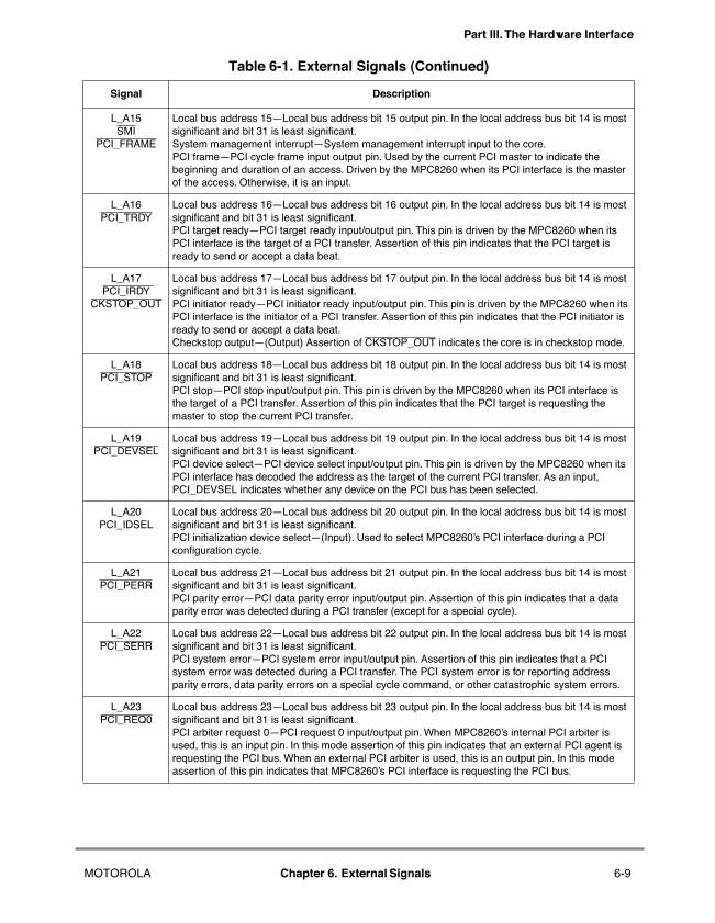
Part III. The Hardware Interface
L_A15SMI
PCI_FRAME
Local bus address 15ÑLocal bus address bit 15 output pin. In the local address bus bit 14 is most signiÞcant and bit 31 is least signiÞcant.System management interruptÑSystem management interrupt input to the core.PCI frameÑPCI cycle frame input output pin. Used by the current PCI master to indicate the beginning and duration of an access. Driven by the MPC8260 when its PCI interface is the master of the access. Otherwise, it is an input.
L_A16PCI_TRDY
Local bus address 16ÑLocal bus address bit 16 output pin. In the local address bus bit 14 is most signiÞcant and bit 31 is least signiÞcant.PCI target readyÑPCI target ready input/output pin. This pin is driven by the MPC8260 when its PCI interface is the target of a PCI transfer. Assertion of this pin indicates that the PCI target is ready to send or accept a data beat.
L_A17PCI_IRDY
CKSTOP_OUT
Local bus address 17ÑLocal bus address bit 17 output pin. In the local address bus bit 14 is most signiÞcant and bit 31 is least signiÞcant.PCI initiator readyÑPCI initiator ready input/output pin. This pin is driven by the MPC8260 when its PCI interface is the initiator of a PCI transfer. Assertion of this pin indicates that the PCI initiator is ready to send or accept a data beat.Checkstop outputÑ(Output) Assertion of CKSTOP_OUT indicates the core is in checkstop mode.
L_A18PCI_STOP
Local bus address 18ÑLocal bus address bit 18 output pin. In the local address bus bit 14 is most signiÞcant and bit 31 is least signiÞcant.PCI stopÑPCI stop input/output pin. This pin is driven by the MPC8260 when its PCI interface is the target of a PCI transfer. Assertion of this pin indicates that the PCI target is requesting the master to stop the current PCI transfer.
L_A19PCI_DEVSEL
Local bus address 19ÑLocal bus address bit 19 output pin. In the local address bus bit 14 is most signiÞcant and bit 31 is least signiÞcant.PCI device selectÑPCI device select input/output pin. This pin is driven by the MPC8260 when its PCI interface has decoded the address as the target of the current PCI transfer. As an input, PCI_DEVSEL indicates whether any device on the PCI bus has been selected.
L_A20PCI_IDSEL
Local bus address 20ÑLocal bus address bit 20 output pin. In the local address bus bit 14 is most signiÞcant and bit 31 is least signiÞcant.PCI initialization device selectÑ(Input). Used to select MPC8260Õs PCI interface during a PCI conÞguration cycle.
L_A21PCI_PERR
Local bus address 21ÑLocal bus address bit 21 output pin. In the local address bus bit 14 is most signiÞcant and bit 31 is least signiÞcant.PCI parity errorÑPCI data parity error input/output pin. Assertion of this pin indicates that a data parity error was detected during a PCI transfer (except for a special cycle).
L_A22PCI_SERR
Local bus address 22ÑLocal bus address bit 22 output pin. In the local address bus bit 14 is most signiÞcant and bit 31 is least signiÞcant.PCI system errorÑPCI system error input/output pin. Assertion of this pin indicates that a PCI system error was detected during a PCI transfer. The PCI system error is for reporting address parity errors, data parity errors on a special cycle command, or other catastrophic system errors.
L_A23PCI_REQ0
Local bus address 23ÑLocal bus address bit 23 output pin. In the local address bus bit 14 is most signiÞcant and bit 31 is least signiÞcant.PCI arbiter request 0ÑPCI request 0 input/output pin. When MPC8260Õs internal PCI arbiter is used, this is an input pin. In this mode assertion of this pin indicates that an external PCI agent is requesting the PCI bus. When an external PCI arbiter is used, this is an output pin. In this mode assertion of this pin indicates that MPC8260Õs PCI interface is requesting the PCI bus.
Table 6-1. External Signals (Continued)
Signal Description
MOTOROLA Chapter 6. External Signals 6-9
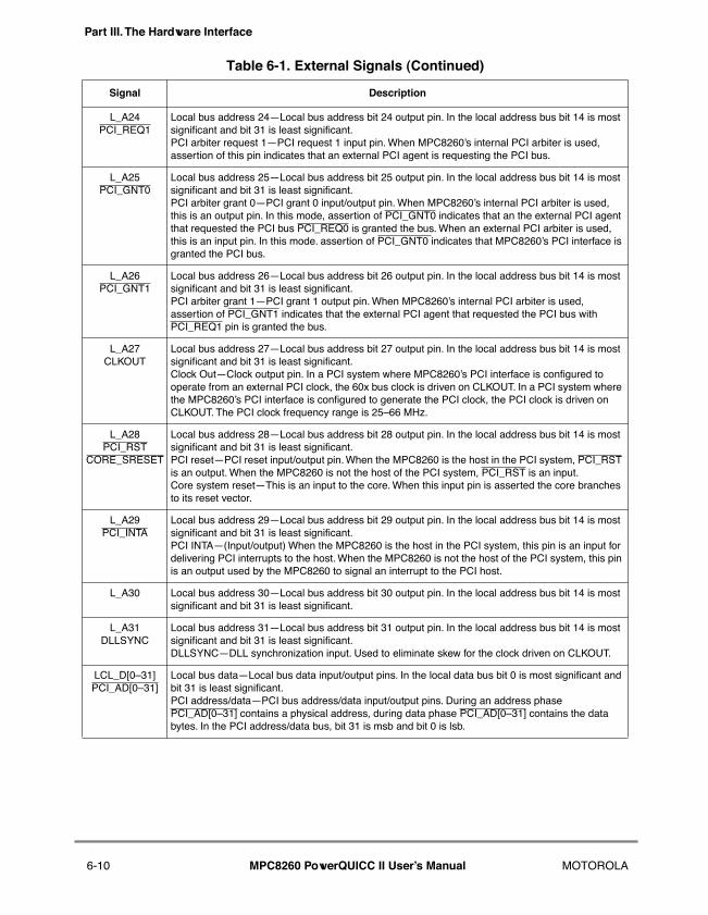
Part III. The Hardware Interface
L_A24PCI_REQ1
Local bus address 24ÑLocal bus address bit 24 output pin. In the local address bus bit 14 is most signiÞcant and bit 31 is least signiÞcant.PCI arbiter request 1ÑPCI request 1 input pin. When MPC8260Õs internal PCI arbiter is used, assertion of this pin indicates that an external PCI agent is requesting the PCI bus.
L_A25PCI_GNT0
Local bus address 25ÑLocal bus address bit 25 output pin. In the local address bus bit 14 is most signiÞcant and bit 31 is least signiÞcant.PCI arbiter grant 0ÑPCI grant 0 input/output pin. When MPC8260Õs internal PCI arbiter is used, this is an output pin. In this mode, assertion of PCI_GNT0 indicates that an the external PCI agent that requested the PCI bus PCI_REQ0 is granted the bus. When an external PCI arbiter is used, this is an input pin. In this mode. assertion of PCI_GNT0 indicates that MPC8260Õs PCI interface is granted the PCI bus.
L_A26PCI_GNT1
Local bus address 26ÑLocal bus address bit 26 output pin. In the local address bus bit 14 is most signiÞcant and bit 31 is least signiÞcant.PCI arbiter grant 1ÑPCI grant 1 output pin. When MPC8260Õs internal PCI arbiter is used, assertion of PCI_GNT1 indicates that the external PCI agent that requested the PCI bus with PCI_REQ1 pin is granted the bus.
L_A27CLKOUT
Local bus address 27ÑLocal bus address bit 27 output pin. In the local address bus bit 14 is most signiÞcant and bit 31 is least signiÞcant.Clock OutÑClock output pin. In a PCI system where MPC8260Õs PCI interface is conÞgured to operate from an external PCI clock, the 60x bus clock is driven on CLKOUT. In a PCI system where the MPC8260Õs PCI interface is conÞgured to generate the PCI clock, the PCI clock is driven on CLKOUT. The PCI clock frequency range is 25Ð66 MHz.
L_A28PCI_RST
CORE_SRESET
Local bus address 28ÑLocal bus address bit 28 output pin. In the local address bus bit 14 is most signiÞcant and bit 31 is least signiÞcant.PCI resetÑPCI reset input/output pin. When the MPC8260 is the host in the PCI system, PCI_RST is an output. When the MPC8260 is not the host of the PCI system, PCI_RST is an input. Core system resetÑThis is an input to the core. When this input pin is asserted the core branches to its reset vector.
L_A29PCI_INTA
Local bus address 29ÑLocal bus address bit 29 output pin. In the local address bus bit 14 is most signiÞcant and bit 31 is least signiÞcant.PCI INTAÑ(Input/output) When the MPC8260 is the host in the PCI system, this pin is an input for delivering PCI interrupts to the host. When the MPC8260 is not the host of the PCI system, this pin is an output used by the MPC8260 to signal an interrupt to the PCI host.
L_A30 Local bus address 30ÑLocal bus address bit 30 output pin. In the local address bus bit 14 is most signiÞcant and bit 31 is least signiÞcant.
L_A31DLLSYNC
Local bus address 31ÑLocal bus address bit 31 output pin. In the local address bus bit 14 is most signiÞcant and bit 31 is least signiÞcant.DLLSYNCÑDLL synchronization input. Used to eliminate skew for the clock driven on CLKOUT.
LCL_D[0Ð31]PCI_AD[0Ð31]
Local bus dataÑLocal bus data input/output pins. In the local data bus bit 0 is most signiÞcant and bit 31 is least signiÞcant.PCI address/dataÑPCI bus address/data input/output pins. During an address phase PCI_AD[0Ð31] contains a physical address, during data phase PCI_AD[0Ð31] contains the data bytes. In the PCI address/data bus, bit 31 is msb and bit 0 is lsb.
Table 6-1. External Signals (Continued)
Signal Description
6-10 MPC8260 PowerQUICC II UserÕs Manual MOTOROLA
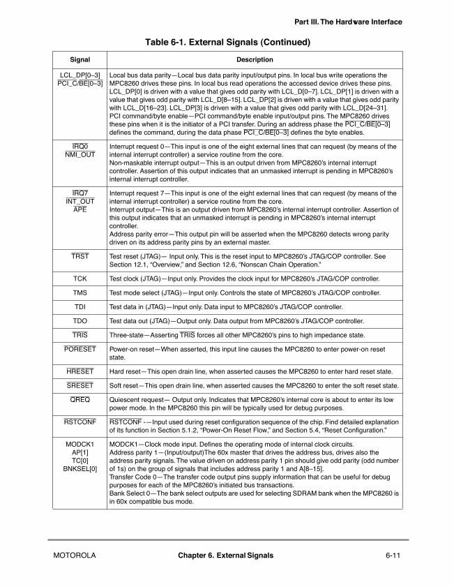
Part III. The Hardware Interface
LCL_DP[0Ð3]PCI_C/BE[0Ð3]
Local bus data parityÑLocal bus data parity input/output pins. In local bus write operations the MPC8260 drives these pins. In local bus read operations the accessed device drives these pins. LCL_DP[0] is driven with a value that gives odd parity with LCL_D[0Ð7]. LCL_DP[1] is driven with a value that gives odd parity with LCL_D[8Ð15]. LCL_DP[2] is driven with a value that gives odd parity with LCL_D[16Ð23]. LCL_DP[3] is driven with a value that gives odd parity with LCL_D[24Ð31]. PCI command/byte enableÑPCI command/byte enable input/output pins. The MPC8260 drives these pins when it is the initiator of a PCI transfer. During an address phase the PCI_C/BE[0Ð3] deÞnes the command, during the data phase PCI_C/BE[0Ð3] deÞnes the byte enables.
IRQ0NMI_OUT
Interrupt request 0ÑThis input is one of the eight external lines that can request (by means of the internal interrupt controller) a service routine from the core. Non-maskable interrupt outputÑThis is an output driven from MPC8260Õs internal interrupt controller. Assertion of this output indicates that an unmasked interrupt is pending in MPC8260Õs internal interrupt controller.
IRQ7INT_OUT
APE
Interrupt request 7ÑThis input is one of the eight external lines that can request (by means of the internal interrupt controller) a service routine from the core.Interrupt outputÑThis is an output driven from MPC8260Õs internal interrupt controller. Assertion of this output indicates that an unmasked interrupt is pending in MPC8260Õs internal interrupt controller.Address parity errorÑThis output pin will be asserted when the MPC8260 detects wrong parity driven on its address parity pins by an external master.
TRST Test reset (JTAG)Ñ Input only. This is the reset input to MPC8260Õs JTAG/COP controller. See Section 12.1, ÒOverview,Ó and Section 12.6, ÒNonscan Chain Operation.Ó
TCK Test clock (JTAG)ÑInput only. Provides the clock input for MPC8260Õs JTAG/COP controller.
TMS Test mode select (JTAG)ÑInput only. Controls the state of MPC8260Õs JTAG/COP controller.
TDI Test data in (JTAG)ÑInput only. Data input to MPC8260Õs JTAG/COP controller.
TDO Test data out (JTAG)ÑOutput only. Data output from MPC8260Õs JTAG/COP controller.
TRIS Three-stateÑAsserting TRIS forces all other MPC8260Õs pins to high impedance state.
PORESET Power-on resetÑWhen asserted, this input line causes the MPC8260 to enter power-on reset state.
HRESET Hard resetÑThis open drain line, when asserted causes the MPC8260 to enter hard reset state.
SRESET Soft resetÑThis open drain line, when asserted causes the MPC8260 to enter the soft reset state.
QREQ Quiescent requestÑ Output only. Indicates that MPC8260Õs internal core is about to enter its low power mode. In the MPC8260 this pin will be typically used for debug purposes.
RSTCONF RSTCONF -ÑInput used during reset conÞguration sequence of the chip. Find detailed explanation of its function in Section 5.1.2, ÒPower-On Reset Flow,Ó and Section 5.4, ÒReset ConÞguration.Ó
MODCK1AP[1]TC[0]
BNKSEL[0]
MODCK1ÑClock mode input. DeÞnes the operating mode of internal clock circuits.Address parity 1Ñ(Input/output)The 60x master that drives the address bus, drives also the address parity signals. The value driven on address parity 1 pin should give odd parity (odd number of 1s) on the group of signals that includes address parity 1 and A[8Ð15].Transfer Code 0ÑThe transfer code output pins supply information that can be useful for debug purposes for each of the MPC8260Õs initiated bus transactions.Bank Select 0ÑThe bank select outputs are used for selecting SDRAM bank when the MPC8260 is in 60x compatible bus mode.
Table 6-1. External Signals (Continued)
Signal Description
MOTOROLA Chapter 6. External Signals 6-11
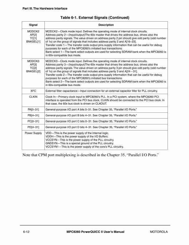
Part III. The Hardware Interface
Note that CPM port multiplexing is described in the Chapter 35, ÒParallel I/O Ports.Ó
MODCK2AP[2]TC[1]
BNKSEL[1]
MODCK2ÑClock mode input. DeÞnes the operating mode of internal clock circuits.Address parity 2Ñ(Input/output)The 60x master that drives the address bus, drives also the address parity signals. The value driven on address parity 2 pin should give odd parity (odd number of 1s) on the group of signals that includes address parity 2 and A[16Ð23].Transfer code 1ÑThe transfer code output pins supply information that can be useful for debug purposes for each of the MPC8260Õs initiated bus transactions.Bank select 1ÑThe bank select outputs are used for selecting SDRAM bank when the MPC8260 is in 60x-compatible bus mode.
MODCK3AP[3]TC[2]
BNKSEL[2]
MODCK3ÑClock mode input. DeÞnes the operating mode of internal clock circuits.Address parity 3Ñ(Input/output)The 60x master that drives the address bus, drives also the address parity signals. The value driven on address parity 3 pin should give odd parity (odd number of 1s) on the group of signals that includes address parity 3 and A[24Ñ31].Transfer code 2ÑThe transfer code output pins supply information that can be useful for debug purposes for each of the MPC8260Õs initiated bus transactions.Bank select 2ÑThe bank select outputs are used for selecting SDRAM bank when the MPC8260 is in 60x-compatible bus mode.
XFC External Þlter capacitanceÑInput connection for an external capacitor Þlter for PLL circuitry.
CLKIN Clock InÑPrimary clock input to MPC8260Õs PLL. In a PCI system, where the MPC8260 PCI interface is operated from the PCI bus clock, CLKIN should be connected to the PCI bus clock. In that case, the 60x bus clock is driven on CLKOUT.
PA[0Ð31] General-purpose I/O port A bits 0Ð31. See Chapter 35, ÒParallel I/O Ports.Ó
PB[4Ð31] General-purpose I/O port B bits 4Ð31. See Chapter 35, ÒParallel I/O Ports.Ó
PC[0Ð31] General-purpose I/O port C bits 0Ð31. See Chapter 35, ÒParallel I/O Ports.Ó
PD[4Ð31] General-purpose I/O port D bits 4Ð31. See Chapter 35, ÒParallel I/O Ports.Ó
Power Supply VDDÑThis is the power supply of the internal logic.VDDHÑThis is the power supply of the I/O Buffers. VCCSYNÑThis is the power supply of the PLL circuitry. GNDSYNÑThis is a special ground of the PLL circuitry. VCCSYN1ÑThis is the power supply of the coreÕs PLL circuitry.
Table 6-1. External Signals (Continued)
Signal Description
6-12 MPC8260 PowerQUICC II UserÕs Manual MOTOROLA
Chapter 7 60x Signals7070
This chapter describes the MPC8260 PowerPC processorÕs external signals. It contains aconcise description of individual signals, showing behavior when a signal is asserted andnegated, when the signal is an input and an output, and the differences in how signals workin external-master or internal-only conÞgurations.
NOTEA bar over a signal name indicates that the signal is active lowÐfor example, ARTRY (address retry) and TS (transfer start).Active-low signals are referred to as asserted (active) whenthey are low and negated when they are high. Signals that arenot active-low, such as TSIZ[0Ð3] (transfer size signals) andTT[0Ð4] (transfer type signals) are referred to as asserted whenthey are high and negated when they are low.
The 60x bus signals used with MPC8260 are grouped as follows:
¥ Address arbitration signalsÑIn external arbiter mode, MPC8260 uses these signals to arbitrate for address bus mastership. The MPC8260 arbiter uses these signals to enable an external device to arbitrate for address bus mastership.
¥ Address transfer start signalsÑThese signals indicate that a bus master has begun a transaction on the address bus.
¥ Address transfer signals (address bus)ÑThese signals are used to transfer the address.
¥ Transfer attribute signalsÑThese signals provide information about the type of transfer, such as the transfer size and whether the transaction is single, single extended, bursted, write-through or cache-inhibited.
¥ Address transfer termination signalsÑThese signals are used to acknowledge the end of the address phase of the transaction. They also indicate whether a condition exists that requires the address phase to be repeated.
¥ Data arbitration signalsÑThe MPC8260, in external arbiter mode, uses these signals to arbitrate for data bus mastership. The MPC8260 arbiter uses these signals to enable an external device to arbitrate for data bus mastership.
MOTOROLA Chapter 7. 60x Signals 7-1
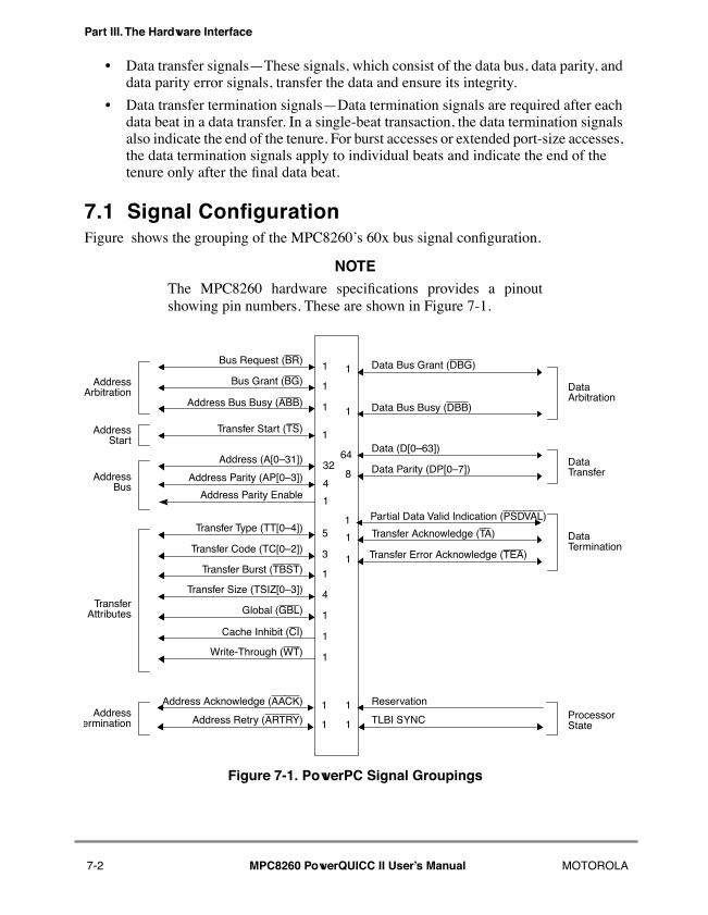
Part III. The Hardware Interface
¥ Data transfer signalsÑThese signals, which consist of the data bus, data parity, and data parity error signals, transfer the data and ensure its integrity.
¥ Data transfer termination signalsÑData termination signals are required after each data beat in a data transfer. In a single-beat transaction, the data termination signals also indicate the end of the tenure. For burst accesses or extended port-size accesses, the data termination signals apply to individual beats and indicate the end of the tenure only after the Þnal data beat.
7.1 Signal ConÞgurationFigure shows the grouping of the MPC8260Õs 60x bus signal conÞguration.
NOTEThe MPC8260 hardware speciÞcations provides a pinoutshowing pin numbers. These are shown in Figure 7-1.
Figure 7-1. PowerPC Signal Groupings
Bus Request (BR)
Bus Grant (BG)
Address Bus Busy (ABB)
Transfer Start (TS)
Address Parity (AP[0Ð3])
Transfer Size (TSIZ[0Ð3])
Transfer Burst (TBST)
Cache Inhibit (CI)
Write-Through (WT)
Address Acknowledge (AACK)
Address Retry (ARTRY)
Data Bus Grant (DBG)
Data Bus Busy (DBB)
Data (D[0Ð63])
Data Parity (DP[0Ð7])
Transfer Acknowledge (TA)
Transfer Error Acknowledge (TEA)
Reservation
1
1
1
1
1
64
8
1
1
1
4
5
4
1
1
1
1
1
Data
Data
Data
Processor
Address
Address
Address
TransferAttributes
Addressermination
1
Transfer Type (TT[0Ð4])
Global (GBL) 1
TLBI SYNC 1
Partial Data Valid Indication (PSDVAL)1
3Transfer Code (TC[0Ð2])
Address (A[0Ð31])32
Address Parity Enable1
State
Termination
Transfer
ArbitrationArbitration
Start
Bus
7-2 MPC8260 PowerQUICC II UserÕs Manual MOTOROLA
Part III. The Hardware Interface
7.2 Signal Descriptions This section describes individual MPC8260 60x signals, grouped according to Figure 7-1.Note that the following sections brießy summarize signal functions. Chapter 8, ÒThe 60xBus,Ó describes many of these signals in greater detail, both in terms of their function andhow groups of signals interact.
7.2.1 Address Bus Arbitration SignalsThe address arbitration signals are a collection of input and output signals devices use torequest address bus mastership, recognize when the request is granted, and indicate to otherdevices when mastership is granted. For a detailed description of how these signals interact,see Section 8.4.1, ÒAddress Arbitration.Ó
Bus arbitration signals have no meaning in internal-only mode.
7.2.1.1 Bus Request (BR)ÑOutputThe bus request (BR) signal is both an input and an output signal on the MPC8260.
7.2.1.1.1 Address Bus Request (BR)ÑOutputFollowing are the state meaning and timing comments for the BR signal output in externalmaster mode.
State Meaning AssertedÑIndicates that MPC8260 is requesting mastership of the address bus. Note that BR may be asserted for one or more cycles and then deasserted due to an internal cancellation of the bus request (for example, due to a load hit in the touch load buffer). See Section 8.4.1, ÒAddress Arbitration.Ó
NegatedÑIndicates that the MPC8260 is not requesting the address bus. The MPC8260 may have no bus operation pending, it may be parked, or the ARTRY input was asserted on the previous bus clock cycle.
Timing Comments AssertionÑMay occur on any cycle; does not occur if the MPC8260 is parked and the address bus is idle (BG asserted and ABB input negated).
NegationÑOccurs for at least one cycle following a qualiÞed BG even if another transaction is pending; also negated for at least one cycle following any qualiÞed ARTRY on the bus unless MPC8260 asserted ARTRY and requires a snoop copyback; may also be negated if MPC8260 cancels the bus request internally before receiving a qualiÞed BG.
High ImpedanceÑOccurs during a hard reset or checkstop condition
MOTOROLA Chapter 7. 60x Signals 7-3
Part III. The Hardware Interface
7.2.1.1.2 Address Bus Request (BR)ÑInputFollowing are the state meaning and timing comments for the BR signal input in externalmaster mode.
State Meaning AssertedÑIndicates that the external master has a bus transaction to perform and is waiting for a qualiÞed BG to begin the address tenure. BR may be asserted even if the two possible pipelined address tenures have already been granted.
NegatedÑIndicates that the external master has no bus transaction to perform, or if the device is parked, that it is potentially ready to start a bus transaction on the next clock cycle (with proper qualiÞcation, see BG).
Timing Comments AssertionÑMay occur on any cycle; does not occur if the external master is parked and the address bus is idle (BG asserted and ABB input negated).
NegationÑOccurs for at least one cycle after a qualiÞed BG even if another transaction is pending; also negated for at least one cycle following any qualiÞed ARTRY on the bus unless this chip asserted the ARTRY and requires to perform a snoop copyback; may also be negated if the external master cancels a bus request internally before receiving a qualiÞed BG.
High ImpedanceÑOccurs during a hard reset or checkstop condition.
7.2.1.2 Bus Grant (BG)The address bus grant (BG) signal is both an input and an output signal.
7.2.1.2.1 Bus Grant (BG)ÑInputThe following are the state meaning and timing comments for the BG signal input inexternal master mode.
State Meaning AssertedÑIndicates that the MPC8260 may, with the proper qualiÞcation, begin a bus transaction and assume ownership of the address bus. A qualiÞed bus grant is generally determined from the bus state as follows: QBG = BG ¥ ÂABB ¥ ÂARTRY where ARTRY is asserted only during the cycle after AACK. Note that the assertion of BR is not required for a qualiÞed bus grant (for bus parking).
NegatedÑIndicates that the MPC8260 is not granted next address ownership.
Timing Comments AssertionÑMay occur on any cycle. Once the MPC8260 has assumed address bus ownership, it does not begin checking for BG again until the cycle after AACK.
7-4 MPC8260 PowerQUICC II UserÕs Manual MOTOROLA
Part III. The Hardware Interface
NegationÑMay occur whenever the MPC8260 must be prevented from using the address bus. The MPC8260 may still assume address bus ownership on the cycle BG is negated if it was asserted the previous cycle with other bus grant qualiÞcations.
7.2.1.2.2 Bus Grant (BG)ÑOutputFollowing are the state meaning and timing comments for the BG signal output in externalmaster mode.
State Meaning AssertedÑIndicates that the external device may, with the proper qualiÞcation, begin a bus transaction and assume ownership of the address bus. A qualiÞed bus grant is generally determined from the bus state as follows: QBG = BG ¥ ÂABB ¥ ÂARTRY where ARTRY is asserted only during the cycle after AACK. Note that the assertion of BR is not required for a qualiÞed bus grant (for bus parking).
NegatedÑIndicates that the external device is not granted next address ownership.
Timing Comments AssertionÑMay occur on any cycle. Once the external device has assumed address bus ownership, it does not begin checking for BG again until the cycle after AACK.
NegationÑMay occur when an external device must be kept from using the address bus. The external device may still assume address bus ownership on the cycle that BG is negated if it was asserted the previous cycle with other bus grant qualiÞcations.
7.2.1.3 Address Bus Busy (ABB)The address bus busy (ABB) signal is both an input and an output signal.
7.2.1.3.1 Address Bus Busy (ABB)ÑOutputFollowing are the state meaning and timing comments for the ABB output signal.
State Meaning AssertedÑIndicates that the MPC8260 is the current address bus master. The MPC8260 may not assume address bus ownership in case a bus request is internally cancelled by the cycle a qualiÞed BG would have been recognized.
NegatedÑIndicates that MPC8260 is not the current address bus master.
Timing Comments AssertionÑOccurs the cycle after a qualiÞed BG is accepted by MPC8260 and remains asserted for the duration of the address tenure.
Turn-Off SequencingÑNegates for a fraction of a bus cycle (1/2 minimum, depends on clock mode) starting the cycle following the assertion of AACK. It then goes to the high impedance state.
MOTOROLA Chapter 7. 60x Signals 7-5
Part III. The Hardware Interface
7.2.1.3.2 Address Bus Busy (ABB)ÑInputFollowing are the state meaning and timing comments for the ABB input signal.
State Meaning AssertedÑIndicates that external device is the address bus master.
NegatedÑIndicates that the address bus may be available for use by the MPC8260 (see BG). The MPC8260 also tracks the state of ABB on the bus from the TS and AACK inputs. (See section on address arbitration phase.)
Timing Comments AssertionÑMay occur whenever the MPC8260 must be prevented from using the address bus.
NegationÑMay occur whenever the MPC8260 may use the address bus.
7.2.2 Address Transfer Start SignalIn the internal only mode the address transfer start signal has no meaning.
Address transfer start signal are input and output signals that indicate that an address bustransfer has begun.
7.2.2.1 Transfer Start (TS)The TS signal is both an input and an output signal on the MPC8260.
7.2.2.1.1 Transfer Start (TS)ÑOutputFollowing are the state meaning and timing comments for the TS output signal.
State Meaning AssertedÑIndicates that the MPC8260 has started a bus transaction and that the address bus and transfer attribute signals are valid. It is also an implied data bus request if the transfer attributes TT[0Ð4] indicate that a data tenure is required for the transaction.
NegatedÑHas no special meaning during a normal transaction.
Timing Comments Assertion/NegationÑDriven and asserted on the cycle after a qualiÞed BG is accepted by MPC8260; remains asserted for one clock only. Negated for the remainder of the address tenure. Assertion is coincident with the Þrst clock that ABB is asserted.
High ImpedanceÑOccurs the cycle following the assertion of AACK (same cycle as ABB negation).
7.2.2.2 Transfer Start (TS)ÑInputFollowing are the state meaning and timing comments for the TS input signal.
State Meaning AssertedÑIndicates that another device has begun a bus transaction and that the address bus and transfer attribute signals are valid for snooping.
NegatedÑHas no special meaning.
7-6 MPC8260 PowerQUICC II UserÕs Manual MOTOROLA
Part III. The Hardware Interface
Timing Comments Assertion/NegationÑMust be asserted for one cycle only and then immediately negated. Assertion may occur at any time during the assertion of ABB.
7.2.3 Address Transfer SignalsIn internal only mode the memory controller uses these signals for glueless addresstransfers to memory and I/O devices.
The address transfer signals are used to transmit the address.
7.2.3.1 Address Bus (A[0Ð31])The address bus (A[0Ð31]) consists of 32 signals that are both input and output signals.
7.2.3.1.1 Address Bus (A[0Ð31])ÑOutputFollowing are the state meaning and timing comments for the A[0Ð31] output signals.
State Meaning ContentÑSpeciÞes the physical address of the bus transaction. For burst or extended operations, the address is a double-word.
Timing Comments Assertion/NegationÑDriven valid on the same cycle that TS is driven/asserted; remains driven/valid for the duration of the address tenure.
High ImpedanceÑ Occurs the cycle following the assertion of AACK; no precharge action performed on release.
7.2.3.1.2 Address Bus (A[0Ð31])ÑInputFollowing are the state meaning and timing comments for the A[0Ð31] input signals.
State Meaning AssertedÑIndicates that another device has begun a bus transaction and that the address bus and transfer attribute signals are valid for snooping and in slave mode.
NegatedÑHas no special meaning.
Timing Comments Assertion/NegationÑMust be valid on the same cycle that TS is asserted; sampled by the processor only on this cycle.
7.2.4 Address Transfer Attribute SignalsIn internal only mode the address transfer attribute signals have no meaning.
The transfer attribute signals are a set of signals that further characterize the transferÑsuchas the size of the transfer, whether it is a read or write operation, and whether it is a burstor single-beat transfer. For a detailed description of how these signals interact, seeSection 7.2.4, ÒAddress Transfer Attribute Signals.Ó
MOTOROLA Chapter 7. 60x Signals 7-7
Part III. The Hardware Interface
7.2.4.1 Transfer Type (TT[0Ð4])The transfer type signals (TT[0Ð4]) consist of Þve input/output signals on the MPC8260.For a complete description of TT[0Ð4] signals and transfer type encoding, seeSection 8.4.3.1, ÒTransfer Type Signal (TT[0Ð4]) Encoding.Ó
7.2.4.1.1 Transfer Type (TT[0Ð4])ÑOutputFollowing are the state meaning and timing comments for the TT[0Ð4] output signals onthe MPC8260.
State Meaning Asserted/NegatedÑSpeciÞes the type of transfer in progress.
Timing Comments Assertion/NegationÑSame as A[0Ð31].
High ImpedanceÑSame as A[0Ð31].
7.2.4.1.2 Transfer Type (TT[0Ð4])ÑInputFollowing are the state meaning and timing comments for the TT[0Ð4] input signals on theMPC8260.
State Meaning Asserted/NegatedÑSpeciÞes the type of transfer in progress for snooping by the MPC8260
Timing Comments Assertion/NegationÑSame as A[0Ð31].
7.2.4.2 Transfer Size (TSIZ[0Ð3])The transfer size (TSIZ[0Ð3]) signals consist of four input/output signals on the MPC8260,following are the state meaning and timing comments for the TSIZ[0Ð3] signals on theMPC8260.
State Meaning Asserted/NegatedÑSpeciÞes the data transfer size for the transaction (see Section 8.4.3.3, ÒTBST and TSIZ[0Ð3] Signals and Size of TransferÓ). During graphics transfer operations, these signals form part of the Resource ID (see TBST).
Timing Comments Assertion/NegationÑSame as A[0Ð31].
High ImpedanceÑSame as A[0Ð31].
7.2.4.3 Transfer Burst (TBST)The transfer burst (TBST) signal is an input/output signal on the MPC8260. Following arethe state meaning and timing comments for the TBST output/input signal.
State Meaning AssertedÑIndicates that a burst transfer is in progress (see Section 8.4.3.3, ÒTBST and TSIZ[0Ð3] Signals and Size of TransferÓ). During graphics transfer operations, this signal forms part of the Resource ID Þeld from the EAR as follows:
TBST || TSIZ[0Ð3] = EAR[28Ð31]. (See TBST.)
NegatedÑIndicates that a burst transfer is not in progress.
Timing Comments Assertion/NegationÑSame as A[0Ð31].
7-8 MPC8260 PowerQUICC II UserÕs Manual MOTOROLA
Part III. The Hardware Interface
High ImpedanceÑSame as A[0Ð31].
7.2.4.4 Global (GBL)The global (GBL) signal is an input/output signal on the MPC8260.
7.2.4.4.1 Global (GBL)ÑOutputFollowing are the state meaning and timing comments for the GBL output signal.
State Meaning AssertedÑIndicates that the transaction is global and should be snooped by other devices. GBL reßects the M bit (WIM bits) from the MMU except during certain transactions.
NegatedÑIndicates that the transaction is not global and should not be snooped by other devices.
Timing Comments Assertion/NegationÑSame as A[0Ð31].
High ImpedanceÑSame as A[0Ð31].
7.2.4.4.2 Global (GBL)ÑInputFollowing are the state meaning and timing comments for the GBL input signal.
State Meaning AssertedÑIndicates that a transaction must be snooped by MPC8260.
NegatedÑIndicates that a transaction should not be snooped by MPC8260. (In addition, certain non-global transactions are snooped for reservation coherency.)
Timing Comments Assertion/NegationÑSame as A[0Ð31].
7.2.4.5 Caching-Inhibited (CI)ÑOutputThe cache inhibit (CI) signal is an output signal on the MPC8260. Following are the statemeaning and timing comments for CI.
State Meaning AssertedÑIndicates that the transaction in progress should not be cached. CI reßects the I bit (WIM bits) from the MMU except during certain transactions.NegatedÑIndicates that the transaction should be cached.
Timing Comments Assertion/NegationÑSame as A[0Ð31].High ImpedanceÑSame as A[0Ð31].
7.2.4.6 Write-Through (WT)ÑOutputThe write-through (WT) signal is an output signal on the MPC8260. Following are the statemeaning and timing comments for WT.
State Meaning AssertedÑIndicates that the transaction should operate in write-through mode. WT reßects the W bit (WIM bits) from the MMU except during certain transactions. WT may be asserted during read transactions.
MOTOROLA Chapter 7. 60x Signals 7-9
Part III. The Hardware Interface
NegatedÑIndicates that the transaction should not operate in write-through mode.
Timing Comments Assertion/NegationÑSame as A[0Ð31].
High ImpedanceÑSame as A[0Ð31].
7.2.5 Address Transfer Termination SignalsThe address transfer termination signals are used to indicate either that the address phaseof the transaction has completed successfully or must be repeated, and when it should beterminated. For detailed information about how these signals interact, see Section 7.2.5,ÒAddress Transfer Termination Signals.Ó
The address transfer termination signals have no meaning in internal only mode.
7.2.5.1 Address Acknowledge (AACK)The address acknowledge (AACK) signal is an input/output on the MPC8260.
7.2.5.1.1 Address Acknowledge (AACK)ÑOutput.Following are the state meaning and timing comments for AACK as an output signal.
State Meaning AssertedÑIndicates that the address tenure of a transaction is terminated. On the cycle following the assertion of AACK, the bus master releases the address-tenure-related signals to the high-impedance state and samples ARTRY.
NegatedÑIndicates that the address bus and the transfer attributes must remain driven, if negated during ABB.
Timing Comments AssertionÑOccurs a programmable number of clocks after TS or whenever ARTRY conditions are resolved.
NegationÑOccurs one clock after assertion.
7.2.5.1.2 Address Acknowledge (AACK)ÑInputFollowing are the state meaning and timing comments for AACK as an input signal.
State Meaning AssertedÑIndicates that a 60x bus slave is terminating the address tenure. On the cycle following the assertion of AACK, the bus master releases the address tenure related signals to the high-impedance state and samples ARTRY.
NegatedÑIndicates that the address tenure must remain active and the address tenure related signals driven.
Timing Comments AssertionÑOccurs during the 60x bus slave access, at least two clocks after TS.
NegationÑOccurs one clock after assertion.
7-10 MPC8260 PowerQUICC II UserÕs Manual MOTOROLA
Part III. The Hardware Interface
7.2.5.2 Address Retry (ARTRY)The address retry (ARTRY) signal is both an input and output signal on the MPC8260
7.2.5.2.1 Address Retry (ARTRY)ÑOutput.Following are the state meaning and timing comments for ARTRY as an output signal.
State Meaning AssertedÑIndicates that the MPC8260 detects a condition in which an address tenure must be retried. If the MPC8260 processor needs to update memory as a result of snoop that caused the retry, the MPC8260 asserts BR the second cycle after AACK if ARTRY is asserted.
High ImpedanceÑIndicates that the MPC8260 does not need the address tenure to be retried.
Timing Comments AssertionÑAsserted the third bus cycle following the assertion of TS if a retry is required.
NegationÑOccurs the second bus cycle after the assertion of AACK. Since this signal may be simultaneously driven by multiple devices, it negates in a unique fashion. First the buffer goes to high impedance for a minimum of one-half processor cycle (dependent on the clock mode), then it is driven negated for one bus cycle before returning to high impedance.
7.2.5.2.2 Address Retry (ARTRY)ÑInputFollowing are the state meaning and timing comments for the ARTRY input.
State Meaning AssertedÑIf the MPC8260 is the address bus master, ARTRY indicates that the MPC8260 must retry the preceding address tenure and immediately negate BR (if asserted). If the associated data tenure has started, the MPC8260 also aborts the data tenure immediately even if the burst data has been received. If the MPC8260 is not the address bus master, this input indicates that the MPC8260 should negate BR for one bus clock cycle immediately after external device asserts ARTRY to permit a copy-back operation to main memory. Note that the subsequent address presented on the address bus may not be the one that generated the assertion of ARTRY.
Negated/High ImpedanceÑIndicates that the MPC8260 does not need to retry the last address tenure.
Timing Comments AssertionÑMay occur as early as the second cycle following the assertion of TS and must occur by the bus clock cycle immediately following the assertion of AACK if an address retry is required.
NegationÑMust occur during the second cycle after the assertion of AACK.
MOTOROLA Chapter 7. 60x Signals 7-11
Part III. The Hardware Interface
7.2.6 Data Bus Arbitration SignalsThe data bus arbitration signals have no meaning in internal-only mode.
Like the address bus arbitration signals, data bus arbitration signals maintain an orderlyprocess for determining data bus mastership. Note that there is no data bus arbitration signalequivalent to the address bus arbitration signal BR (bus request), because, except foraddress-only transactions, TS implies data bus requests. For a detailed description on howthese signals interact, see Section 8.5.1, ÒData Bus Arbitration.Ó
7.2.6.1 Data Bus Grant (DBG)The data bus grant signal (DBG) is an output/input on the MPC8260
7.2.6.1.1 Data Bus Grant (DBG)ÑInputDBG an input when MPC8260 is conÞgured to an external arbiter. The following are thestate meaning and timing comments for DBG.
State Meaning AssertedÑIndicates that the MPC8260 may, with the proper qualiÞcation, assume mastership of the data bus. The MPC8260 derives a qualiÞed data bus grant when DBG is asserted and DBB and ARTRY are negated; that is, the data bus is not busy (DBB is negated), and there is no outstanding attempt to perform an ARTRY of the associated address tenure.
NegatedÑIndicates that the MPC8260 must hold off its data tenures.
Timing Comments AssertionÑMay occur any time to indicate the MPC8260 is free to take data bus mastership. It is not sampled until TS is asserted.
NegationÑMay occur at any time to indicate the MPC8260 cannot assume data bus mastership.
7.2.6.1.2 Data Bus Grant (DBG)ÑOutputDBG signal is output when the MPC8260 conÞgured to Internal Arbiter. Following are thestate meaning and timing comments for the DBG signal.
State Meaning AssertedÑIndicates that the external device may, with the proper qualiÞcation, assume mastership of the data bus. A qualiÞed data bus grant is deÞned as the assertion of DBG, negation of DBB, and negation of ARTRY. The requirement for the ARTRY signal is only for the address bus tenure associated with the data bus tenure about to be granted (that is, not for another address tenure available because of address pipelining).NegatedÑIndicates that an external device is not granted mastership of the data bus.
Timing Comments AssertionÑOccurs on the Þrst clock in which the data bus is not busy and the processor has the highest priority outstanding data transaction.NegationÑOccurs one clock after assertion.
7-12 MPC8260 PowerQUICC II UserÕs Manual MOTOROLA
Part III. The Hardware Interface
7.2.6.2 Data Bus Busy (DBB)The data bus busy (DBB) signal is both an input and output signal on the MPC8260
7.2.6.2.1 Data Bus Busy (DBB)ÑOutputFollowing are the state meaning and timing comments for the DBB output signal.
State Meaning AssertedÑIndicates that the MPC8260 is the data bus master. The MPC8260 always assumes data bus mastership if it needs the data bus and determines a qualiÞed data bus grant (see DBG).
NegatedÑIndicates that the MPC8260 is not using the data bus.
Timing Comments AssertionÑOccurs during the bus clock cycle following a qualiÞed DBG.
NegationÑOccurs for a minimum of one-half bus clock cycle following the assertion of the Þnal TA following TEA or certain ARTRY cases.
High ImpedanceÑOccurs after DBB is negated.
7.2.6.2.2 Data Bus Busy (DBB)ÑInputFollowing are the state meaning and timing comments for the DBB input signal.
State Meaning AssertedÑIndicates that another device is bus master.
NegatedÑIndicates that the data bus is free (with proper qualiÞcation, see DBG) for use by the MPC8260.
Timing Comments AssertionÑMust occur when the MPC8260 must be prevented from using the data bus.
NegationÑMay occur whenever the data bus is available.
7.2.7 Data Transfer SignalsData transfer signals are used in the same way in both internal only and external mastermodes. Like the address transfer signals, the data transfer signals are used to transmit dataand to generate and monitor parity for the data transfer. For a detailed description of howdata transfer signals interact, see Section 7.2.7, ÒData Transfer Signals.Ó
7.2.7.1 Data Bus (D[0Ð63])The data bus (D[0Ð63]) states have the same meanings in both internal only mode externalmaster mode. The data bus consists of 64 signals that are both inputs and outputs on theMPC8260. Following are the state meaning and timing comments for the data bus.
State Meaning The data bus holds 8 byte lanes assigned as shown in Table 7-1.
Timing Comments The number of times the data bus is driven depends on the transfer size, port size, and whether the transfer is a single-beat or burst operation.
MOTOROLA Chapter 7. 60x Signals 7-13
Part III. The Hardware Interface
7.2.7.1.1 Data Bus (D[0Ð63])ÑOutputFollowing are the state meaning and timing comments for the D[0Ð63] output signals.
State Meaning Asserted/NegatedÑRepresents the state of data during a data write. Byte lanes not selected for data transfer do not supply valid data. MPC8260 duplicates data to enable valid data to be sent to different port sizes.
Timing Comments Assertion/NegationÑInitial beat coincides with DBB, for bursts, transitions on the bus clock cycle following each assertion of TA and, for port size, transitions on the bus clock cycle following each assertion of PSDVAL.
High ImpedanceÑOccurs on the bus clock cycle after the Þnal assertion of TA, TEA, or certain ARTRY cases.
7.2.7.1.2 Data Bus (D[0Ð63])ÑInputFollowing are the state meaning and timing comments for the D[0Ð63] input signals.
State Meaning Asserted/NegatedÑRepresents the state of data during a data read transaction.
Timing Comments Assertion/NegationÑData must be valid on the same bus clock cycle that TA and/or PSDVAL is asserted.
7.2.7.2 Data Bus Parity (DP[0Ð7])The eight data bus parity (DP[0Ð7]) signals both output and input signals.
7.2.7.2.1 Data Bus Parity (DP[0Ð7])ÑOutputFollowing are the state meaning and timing comments for the DP[0Ð7] output signals.
State Meaning Asserted/NegatedÑRepresents odd parity for each of 8 bytes of data write transactions. Odd parity means that an odd number of bits, including the parity bit, are driven high. The signal assignments are listed in Table 7-1.
Table 0-1. Data Bus Lane Assignments
Data Bus Signals Byte Lane
D0ÐD7 0
D8ÐD15 1
D16ÐD23 2
D24ÐD31 3
D32ÐD39 4
D40ÐD47 5
D48ÐD55 6
D56ÐD63 7
7-14 MPC8260 PowerQUICC II UserÕs Manual MOTOROLA
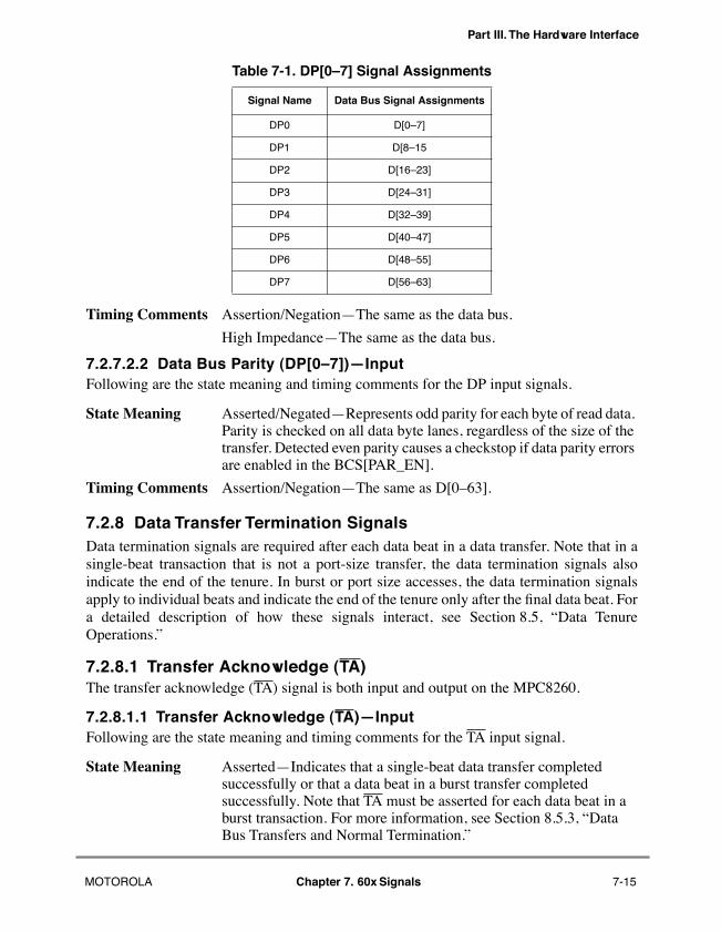
Part III. The Hardware Interface
Timing Comments Assertion/NegationÑThe same as the data bus.
High ImpedanceÑThe same as the data bus.
7.2.7.2.2 Data Bus Parity (DP[0Ð7])ÑInputFollowing are the state meaning and timing comments for the DP input signals.
State Meaning Asserted/NegatedÑRepresents odd parity for each byte of read data. Parity is checked on all data byte lanes, regardless of the size of the transfer. Detected even parity causes a checkstop if data parity errors are enabled in the BCS[PAR_EN].
Timing Comments Assertion/NegationÑThe same as D[0Ð63].
7.2.8 Data Transfer Termination SignalsData termination signals are required after each data beat in a data transfer. Note that in asingle-beat transaction that is not a port-size transfer, the data termination signals alsoindicate the end of the tenure. In burst or port size accesses, the data termination signalsapply to individual beats and indicate the end of the tenure only after the Þnal data beat. Fora detailed description of how these signals interact, see Section 8.5, ÒData TenureOperations.Ó
7.2.8.1 Transfer Acknowledge (TA)The transfer acknowledge (TA) signal is both input and output on the MPC8260.
7.2.8.1.1 Transfer Acknowledge (TA)ÑInputFollowing are the state meaning and timing comments for the TA input signal.
State Meaning AssertedÑIndicates that a single-beat data transfer completed successfully or that a data beat in a burst transfer completed successfully. Note that TA must be asserted for each data beat in a burst transaction. For more information, see Section 8.5.3, ÒData Bus Transfers and Normal Termination.Ó
Table 7-1. DP[0Ð7] Signal Assignments
Signal Name Data Bus Signal Assignments
DP0 D[0Ð7]
DP1 D[8Ð15
DP2 D[16Ð23]
DP3 D[24Ð31]
DP4 D[32Ð39]
DP5 D[40Ð47]
DP6 D[48Ð55]
DP7 D[56Ð63]
MOTOROLA Chapter 7. 60x Signals 7-15
Part III. The Hardware Interface
NegatedÑ(During assertion of DBB) indicates that, until TA is asserted, the MPC8260 must continue to drive the data for the current write or must wait to sample the data for reads.
Timing Comments AssertionÑMust not occur before AACK for the current transaction (if the address retry mechanism is to be used to prevent invalid data from being used by the MPC8260); otherwise, assertion may occur at any time during the assertion of DBB. The system can withhold assertion of TA to indicate that the MPC8260 should insert wait states to extend the duration of the data beat. NegationÑMust occur after the bus clock cycle of the Þnal (or only) data beat of the transfer. For a burst transfer, the system can assert TA for one bus clock cycle and then negate it to advance the burst transfer to the next beat and insert wait states during the next beat. (Note: when conÞgured for 1:1 clock mode and is performing a burst read into the data cache, the MPC8260 requires two wait states between the assertion of TS and the Þrst assertion of TA for that transaction, or one wait state for 1.5:1 clock mode.)
7.2.8.1.2 Transfer Acknowledge (TA)ÑOutputFollowing are the state meaning and timing comments for TA as an output signal.
State Meaning AssertedÑIndicates that the data has been latched for a write operation, or that the data is valid for a read operation, thus terminating the current data beat. If it is the last or only data beat, this also terminates the data tenure. NegatedÑIndicates that master must extend the current data beat (insert wait states) until data can be provided or accepted by the MPC8260.
Timing Comments AssertionÑOccurs on the clock in which the current data transfer can be completed.
NegationÑOccurs after the clock cycle of the Þnal (or only) data beat of the transfer. For a burst transfer, TA may be negated between beats to insert one or more wait states before the completion of the next beat.
7.2.8.2 Transfer Error Acknowledge (TEA)The transfer error acknowledge (TEA) signal is both input and output on the MPC8260,This signal can be ignored if BCR[TEA_EN] is cleared.
7.2.8.2.1 Transfer Error Acknowledge (TEA)ÑInputFollowing are the state meaning and timing comments for the TEA input signal.
State Meaning AssertedÑIndicates that a bus error occurred. The assertion of TEA causes the negation/high impedance of DBB in the next clock cycle. However, data entering the MPC8260 internal memory resources such as GPRs or caches are not invalidated.
7-16 MPC8260 PowerQUICC II UserÕs Manual MOTOROLA
Part III. The Hardware Interface
NegatedÑIndicates that no bus error was detected.
Timing Comments AssertionÑMay be asserted while DBB is asserted and for the cycle after is TA is asserted during a read operation. TEA should be asserted for one cycle only.
NegationÑTEA must be negated no later than the negation of DBB.
7.2.8.2.2 Transfer Error Acknowledge (TEA)ÑOutputFollowing are the state meaning and timing comments for the TEA output.
State Meaning AssertedÑIndicates that a bus error has occurred. Assertion of TEA terminates the transaction in progress; that is, asserting TA is unnecessary because it is ignored by the target device. An unsupported memory transaction, such as a direct-store access or a graphics read or write, causes the assertion of TEA (provided TEA is enabled and the address transfer matches the MPC8260 memory map).
NegatedÑIndicates that no bus error was detected.
Timing Comments AssertionÑOccurs on the Þrst clock after the bus error is detected.
NegationÑOccurs one clock after assertion.
7.2.8.3 Partial Data Valid Indication (PSDVAL)The partial data valid indication (PSDVAL) is both an input and output on the MPC8260
7.2.8.3.1 Partial Data Valid (PSDVAL)ÑInputFollowing are the state meaning and timing comments for the PSDVAL input signal. Notethat TA asserts with PSDVAL to indicate the termination of the current transfer and for eachcomplete data beat in burst transactions.
State Meaning AssertedÑIndicates that a beat data transfer completed successfully. Note that PSDVAL must be asserted for each data beat in a single beat, port size and burst transaction,. For more information, see Section 8.5.5, ÒPort Size Data Bus Transfers and PSDVAL Termination.Ó
NegatedÑ(During DBB) indicates that, until PSDVAL is asserted, the MPC8260 must continue to drive the data for the current write or must wait to sample the data for reads.
Timing Comments AssertionÑMust not occur before AACK for the current transaction (if the address retry mechanism is to be used to prevent invalid data from being used by the MPC8260); otherwise, assertion may occur at any time during the assertion of DBB. The system can withhold assertion of PSDVAL to indicate that the MPC8260 should insert wait states to extend the duration of the data beat.
NegationÑMust occur after the bus clock cycle of the Þnal (or only) data beat of the transfer. For a burst and/or port size transfer, the
MOTOROLA Chapter 7. 60x Signals 7-17
Part III. The Hardware Interface
system can assert PSDVAL for one bus clock cycle and then negate it to insert wait states during the next beat. (Note: when the MPC8260 Processor is conÞgured for 1:1 clock mode and is performing a burst read into the data cache, the MPC8260 requires two wait state between the assertion of TS and the Þrst assertion of PSDVAL for that transaction, or 1 wait state for 1.5:1 clock mode.)
7.2.8.3.2 Partial Data Valid (PSDVAL)ÑOutputFollowing are the state meaning and timing comments for PSDVAL as an output signal.
State Meaning AssertedÑIndicates that the data has been latched for a write operation, or that the data is valid for a read operation, thus terminating the current data beat. If it is the last or only data beat, this also terminates the data tenure.
NegatedÑIndicates that the master must extend the current data beat (insert wait states) until data can be provided or accepted by the MPC8260.
Timing Comments AssertionÑOccurs on the clock in which the current data transfer can be completed.
NegationÑOccurs after the clock cycle of the Þnal (or only) data beat of the transfer. For a burst transfer, PSDVAL may be negated between beats to insert one or more wait states before the completion of the next beat.
7-18 MPC8260 PowerQUICC II UserÕs Manual MOTOROLA
Chapter 8 The 60x Bus8080
The 60x bus, which is used by PowerPC processors, provides ßexible support for the on-chip PowerPC MPC603 processor as well as other internal and external bus devices. The60x bus supports 32-bit addressing, a 64-bit data bus, and burst operations that transfer asmany as 256 bits of data in a four-beat burst. The 60x data bus can be accessed in 8-, 16-,32-, and 64-bit data ports. The 60x bus supports accesses of 1, 2, 3, and 4 bytes, aligned orunaligned, on 4-byte (word) boundaries; it also supports 64-, 128-, 192-, and 256-bitaccesses.
The address and data buses support synchronous, one-level pipeline transactions. The 60xbus interface can be conÞgured to support both external and internal masters or internalmasters only.
8.1 TerminologyTable 8-1 deÞnes terms used in this chapter.
Table 8-1. Terminology
Term DeÞnition
Atomic A bus access that attempts to be part of a read-write operation to the same address uninterrupted by any other access to that address. The MPC8260 initiates the read and write separately, but signals the memory system that it is attempting an atomic operation. If the operation fails, status is kept so that MPC8260 can try again.
Beat A single state on the MPC8260 interface that may extend across multiple bus cycles. (An MPC8260 transaction can be composed of multiple address or data beats.)
Burst A multiple-beat data transfer whose total size is typically equal to a cache block size (in MPC8260: 32 bytes, or 4 data beats at 8 bytes per beat).
Cache block The PowerPC architecture deÞnes the basic unit of coherency as a cache block, which can be considered the same thing as a cache line.
Clean An operation that causes a cache block to be written to memory if modiÞed, and then left in a valid, unmodiÞed state in the cache.
Flush An operation that causes a cache block to be invalidated in the cache, and its data, if modiÞed, to be written back to main memory.
Kill An operation that causes a cache block to be invalidated in the cache without writing any modiÞed data to memory.
MOTOROLA Chapter 8. The 60x Bus 8-1
Part III. The Hardware Interface
8.2 Bus ConÞgurationThe 60x bus supports separate bus conÞgurations for internal masters and external busmasters.
¥ Single-MPC8260 bus mode connects external devices by using only the memory controller. This is described in Section 8.2.1, ÒSingle MPC8260 Bus Mode.Ó
¥ The 60x-compatible bus mode, described in Section 8.2.2, Ò60x-Compatible Bus Mode,Ó enables connections to other masters and 60x-bus slaves, such as an external L2 cache controller.
The Þgures in the following sections show how the MPC8260 can be connected in thesetwo conÞgurations.
8.2.1 Single MPC8260 Bus ModeIn single-MPC8260 bus mode, the MPC8260 is the only bus device in the system. Theinternal memory controller controls all devices on the external pins. Figure 8-1 shows thesignal connections for single-MPC8260 bus mode.
Lane A sub-grouping of signals within a bus. An 8-bit section of the address or data bus may be referred to as a byte lane for that bus.
Master The device that owns the address or data bus, the device that initiates or requests the transaction.
ModiÞed IdentiÞes a cache block The M state in a MESI or MEI protocol.
Parking Granting potential bus mastership without requiring a bus request from that device. This eliminates the arbitration delay associated with the bus request.
Pipelining Initiating a bus transaction before the current one Þnishes. This involves running an address tenure for a new bus transaction before the data tenure for a current bus transaction completes.
Slave The device addressed by the master. The slave is identiÞed in the address tenure and is responsible for sourcing or sinking the requested data for the master during the data tenure.
Snooping Monitoring addresses driven by a bus master to detect the need for coherency actions.
Split-transaction A transaction with separate request and response tenures.
Tenure The period of bus mastership. For MPC8260, there can be separate address bus tenures and data bus tenures.
Transaction A complete exchange between two bus devices. A typical transaction is composed of an address tenure and a data tenure, which may overlap or occur separately from the address tenure. A transaction can minimally consist of an address tenure alone.
Table 8-1. Terminology (Continued)
Term DeÞnition
8-2 MPC8260 PowerQUICC II UserÕs Manual MOTOROLA
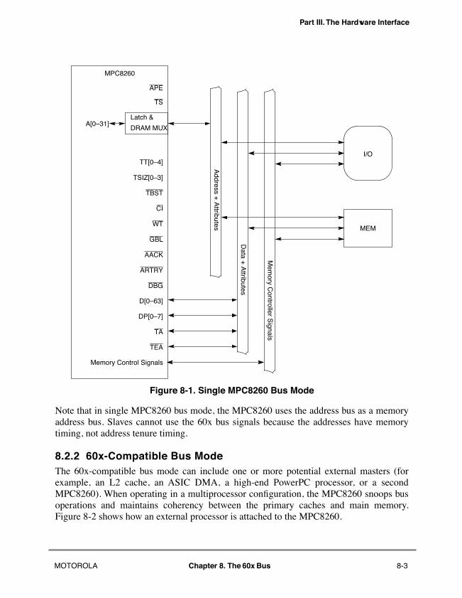
Part III. The Hardware Interface
Figure 8-1. Single MPC8260 Bus Mode
Note that in single MPC8260 bus mode, the MPC8260 uses the address bus as a memoryaddress bus. Slaves cannot use the 60x bus signals because the addresses have memorytiming, not address tenure timing.
8.2.2 60x-Compatible Bus ModeThe 60x-compatible bus mode can include one or more potential external masters (forexample, an L2 cache, an ASIC DMA, a high-end PowerPC processor, or a secondMPC8260). When operating in a multiprocessor conÞguration, the MPC8260 snoops busoperations and maintains coherency between the primary caches and main memory.Figure 8-2 shows how an external processor is attached to the MPC8260.
TS
A[0Ð31]
TT[0Ð4]
TSIZ[0Ð3]
TBST
CI
WT
GBL
AACK
ARTRY
DBG
D[0Ð63]
DP[0Ð7]
TA
TEA
MPC8260
I/O
MEMD
ata + A
ttributes
Address +
Attributes
Latch &
Mem
ory Controller S
ignals
DRAM MUX
Memory Control Signals
APE
MOTOROLA Chapter 8. The 60x Bus 8-3
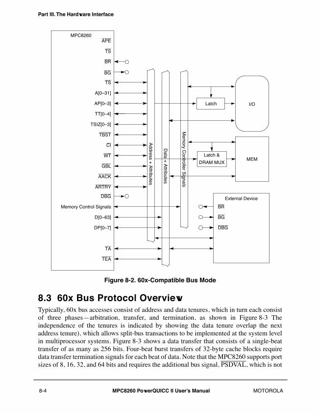
Part III. The Hardware Interface
Figure 8-2. 60x-Compatible Bus Mode
8.3 60x Bus Protocol OverviewTypically, 60x bus accesses consist of address and data tenures, which in turn each consistof three phasesÑarbitration, transfer, and termination, as shown in Figure 8-3 Theindependence of the tenures is indicated by showing the data tenure overlap the nextaddress tenure), which allows split-bus transactions to be implemented at the system levelin multiprocessor systems. Figure 8-3 shows a data transfer that consists of a single-beattransfer of as many as 256 bits. Four-beat burst transfers of 32-byte cache blocks requiredata transfer termination signals for each beat of data. Note that the MPC8260 supports portsizes of 8, 16, 32, and 64 bits and requires the additional bus signal, PSDVAL, which is not
BR
BG
TS
A[0Ð31]
TT[0Ð4]
TSIZ[0Ð3]
TBST
CI
WT
GBL
AACK
ARTRY
DBG
D[0Ð63]
DP[0Ð7]
TA
TEA
MPC8260
I/O
MEMD
ata + A
ttributes
Address +
Attributes
Mem
ory Controller S
ignals
External Device
BR
BG
DBG
Latch
Latch &
DRAM MUX
Memory Control Signals
AP[0Ð3]
TS
APE
8-4 MPC8260 PowerQUICC II UserÕs Manual MOTOROLA
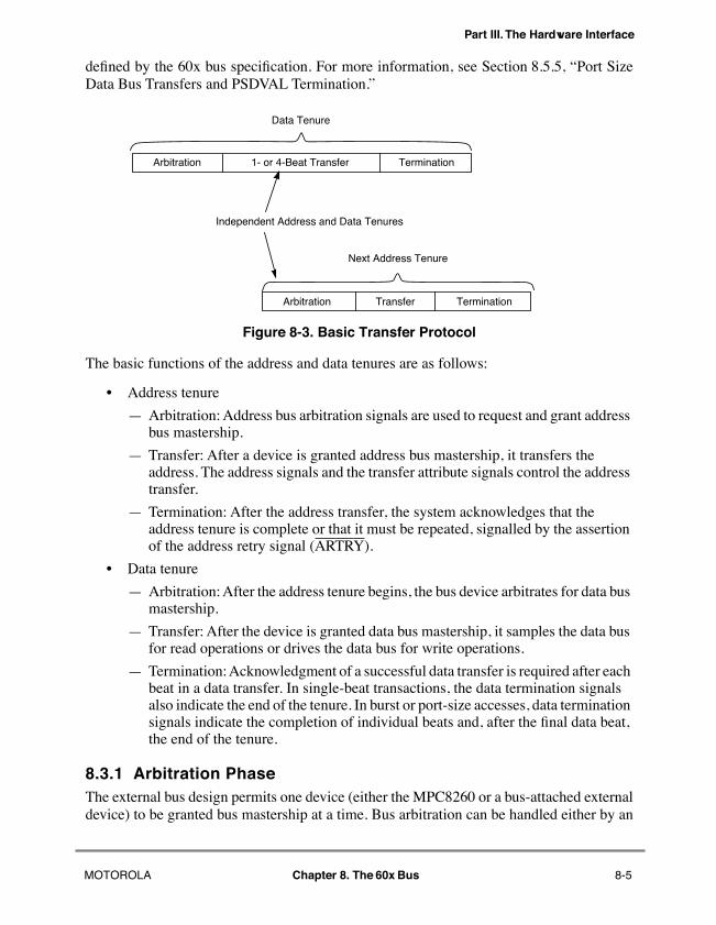
Part III. The Hardware Interface
deÞned by the 60x bus speciÞcation. For more information, see Section 8.5.5, ÒPort SizeData Bus Transfers and PSDVAL Termination.Ó
Figure 8-3. Basic Transfer Protocol
The basic functions of the address and data tenures are as follows:
¥ Address tenure
Ñ Arbitration: Address bus arbitration signals are used to request and grant address bus mastership.
Ñ Transfer: After a device is granted address bus mastership, it transfers the address. The address signals and the transfer attribute signals control the address transfer.
Ñ Termination: After the address transfer, the system acknowledges that the address tenure is complete or that it must be repeated, signalled by the assertion of the address retry signal (ARTRY).
¥ Data tenure
Ñ Arbitration: After the address tenure begins, the bus device arbitrates for data bus mastership.
Ñ Transfer: After the device is granted data bus mastership, it samples the data bus for read operations or drives the data bus for write operations.
Ñ Termination: Acknowledgment of a successful data transfer is required after each beat in a data transfer. In single-beat transactions, the data termination signals also indicate the end of the tenure. In burst or port-size accesses, data termination signals indicate the completion of individual beats and, after the Þnal data beat, the end of the tenure.
8.3.1 Arbitration PhaseThe external bus design permits one device (either the MPC8260 or a bus-attached externaldevice) to be granted bus mastership at a time. Bus arbitration can be handled either by an
Data Tenure
Arbitration 1- or 4-Beat Transfer Termination
Next Address Tenure
Independent Address and Data Tenures
Arbitration Transfer Termination
MOTOROLA Chapter 8. The 60x Bus 8-5
Part III. The Hardware Interface
external central bus arbiter or by the internal on-chip arbiter. In the latter case, the systemis optimized for three external bus masters besides the MPC8260. The arbitrationconÞguration (external or internal) is determined at system reset by sampling conÞgurationpins. See Section 10.9, ÒExternal Master Support (60x-Compatible Mode),Ó for moreinformation.
The MPC8260 controls bus access through the bus request (BR) and bus grant (BG) signals.It determines the state of the address and data bus busy signals by monitoring DBG, TS,AACK, and TA, and it qualiÞes them with ABB and DBB.
The following signals are used for address bus arbitration:
¥ BR (bus request)ÑA device asserts BR to request address bus mastership.
¥ BG (bus grant)ÑAssertion indicates that a bus device may, with proper qualiÞcation, assume mastership of the address bus. A qualiÞed bus grant occurs when BG is asserted while ABB and ARTRY are negated.
¥ ABB (address bus busy)ÑA device asserts ABB to indicate it is the current address bus master. Note that if all devices assert AACK with TS and would normally negate ABB after AACK is asserted, the devices can ignore ABB because the MPC8260 can internally generate ABB. The MPC8260Õs ABB, if enabled, must be tied to a pull-up resistor.
The following signals are used for data bus arbitration:
¥ DBG (data bus grant)ÑIndicates that a bus device can, with the proper qualiÞcation, assume data bus mastership. A qualiÞed data bus grant occurs when DBG is asserted while DBB and ARTRY are negated.
¥ DBB (data bus busy)ÑAssertion by the device indicates that the device is the current data bus master. The device master always assumes data bus mastership if it needs the data bus and is given a qualiÞed data bus grant (see DBG). Note that if all devices assert DBB in conjunction with qualiÞed data bus grant and would normally negate DBB after the last TA is asserted, the devices can ignore DBB because the MPC8260 can generate DBB internally. The MPC8260Õs DBB signal, if enabled, must be tied to a pull-up resistor.
The following is a summary of rules for arbitration:
¥ Preference among devices is determined at the request level. The MPC8260 supports eight levels of bus requests.
¥ When no bus device is requesting the address bus, the MPC8260 parks the device selected in the arbiter conÞguration register on the bus.
For more information, see Section 4.3.2.2, Ò60x Bus Arbiter ConÞguration Register(PPC_ACR).Ó
8-6 MPC8260 PowerQUICC II UserÕs Manual MOTOROLA
Part III. The Hardware Interface
8.3.2 Address Pipelining and Split-Bus TransactionsThe 60x bus protocol provides independent address and data bus capability to supportpipelined and split-bus transaction system organizations. Address pipelining allows thenext address tenure to begin before the current data tenure has Þnished. Although thisability does not inherently reduce memory latency, support for address pipelining and split-bus transactions can greatly improve effective bus/memory throughput. These beneÞts aremost fully realized in shared-memory, multiple-master implementations where busbandwidth is critical to system performance.
External arbitration (as provided by the MPC8260) is required in systems in which multipledevices share the system bus. The MPC8260 uses the address acknowledge (AACK) signalto control pipelining. The MPC8260 supports both one- and zero-level bus pipelining. One-level pipelining is achieved by asserting AACK to the current address bus master andgranting mastership of the address bus to the next requesting master before the current databus tenure has completed. Two address tenures can occur before the current data bus tenurecompletes. The MPC8260 also supports non-pipelined accesses.
8.4 Address Tenure OperationsThis section describes the three phases of the address tenureÑaddress bus arbitration,address transfer, and address termination.
8.4.1 Address ArbitrationBus arbitration can be handled either by an external arbiter or by the internal on-chiparbiter. The arbitration conÞguration (external or internal) is chosen at system reset. Forinternal arbitration, the MPC8260 provides arbitration for the 60x address bus and thesystem is optimized for three external bus masters besides the MPC8260. The bus request(BR) for the external device is an external input to the arbiter. The bus grant signal for theexternal device (BG) is output to the external device.The BG signal asserted by MPC8260Õson-chip arbiter is asserted one clock after the current master on the bus has asserted AACK;therefore, it can be called a qualiÞed BG. Assuming that all potential masters negate ABBone clock after receiving AACK, the device receiving BG can start the address tenure (byasserting TS) one clock after receiving BG. In addition to the external signals, there areinternal request and grant signals for the MPC8260 processor, communications processor,refresh controller, and the PCI internal bridge. Bus accesses are prioritized, withprogrammable priority. When a MPC8260Õs internal master needs the 60x bus, it asserts theinternal bus request along with the request level. The arbiter asserts the internal bus grantfor the highest priority request.
The MPC8260 supports address bus parking through the use of the parked master bits inthe arbiter conÞguration register. The MPC8260 parks the address bus (asserts the addressbus grant signal in anticipation of an address bus request) to the external master or internalmasters. When a device is parked, the arbiter can hold BG asserted for a device even if thatdevice has not requested the bus. Therefore, when the parked device needs to perform a bus
MOTOROLA Chapter 8. The 60x Bus 8-7
Part III. The Hardware Interface
transaction, it skips the bus request delay and assumes address bus mastership on the nextcycle. For this case, BR is not asserted and the access latency seen by the device isshortened by one cycle.
The MPC8260 and external device bus devices qualify BG by sampling ARTRY in thenegated state prior to taking address bus mastership. The negation of ARTRY during theaddress retry window (one cycle after the assertion of AACK) indicates that no addressretry is requested. If a device detects ARTRY asserted, it cannot accept a address bus grantduring the ARTRY cycle or the cycle following. A device that asserts ARTRY due to amodiÞed cache block hit, for example, asserts its bus request during the cycle after theassertion of ARTRY and assumes bus mastership for the cache block push when it is givena bus grant.
The series of address transfers in Figure 8-4 shows the transfer protocol when theMPC8260 is conÞgured in 60x-compatible bus mode. In this example, MPC8260 is initiallyparked on the bus with BG INT-asserted (note that BG INT is an internal signal not seen bythe user at the pins), which lets it start an address bus tenure by asserting TS. During thesame clock cycle, the external masterÕs bus request is asserted to request access to the 60xbus, thereby causing the negation of BG INT internally and the assertion of BG at the pin.Following MPC8260Õs address tenure, the external master takes the bus and initiates itsaddress transaction. The on-chip arbiter samples BR during the clock cycle in which AACKis asserted; if BR is not asserted (no pending request), it negates BG and asserts the parkedbus grant (BG_INT in this example).
The master can assert BR and receive a qualiÞed bus grant without subsequently using thebus. It can negate (cancel) BR before accepting a qualiÞed bus grant. This can occur whena replacement copyback transaction waiting to be run on the bus is killed by a snoop ofanother bus master. This can also occur when the reservation set by a pending stwcx.transaction is cancelled by a snoop of another master. In both cases, the pending transactionby the processor is cancelled and BR is negated.
8-8 MPC8260 PowerQUICC II UserÕs Manual MOTOROLA
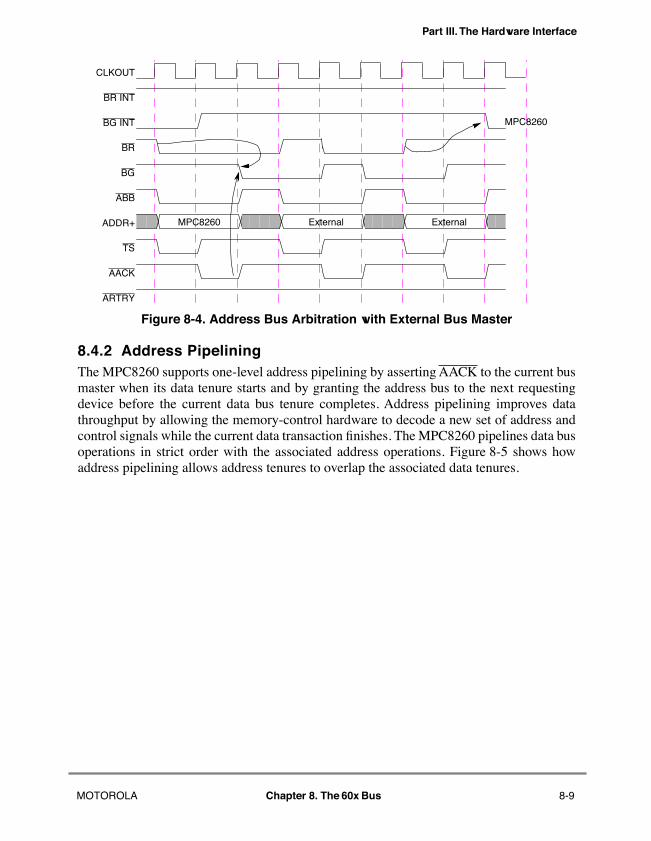
Part III. The Hardware Interface
Figure 8-4. Address Bus Arbitration with External Bus Master
8.4.2 Address PipeliningThe MPC8260 supports one-level address pipelining by asserting AACK to the current busmaster when its data tenure starts and by granting the address bus to the next requestingdevice before the current data bus tenure completes. Address pipelining improves datathroughput by allowing the memory-control hardware to decode a new set of address andcontrol signals while the current data transaction Þnishes. The MPC8260 pipelines data busoperations in strict order with the associated address operations. Figure 8-5 shows howaddress pipelining allows address tenures to overlap the associated data tenures.
CLKOUT
BR INT
BG INT MPC8260
BR
BG
ABB
ADDR+ MPC8260 External External
TS
AACK
ARTRY
MOTOROLA Chapter 8. The 60x Bus 8-9
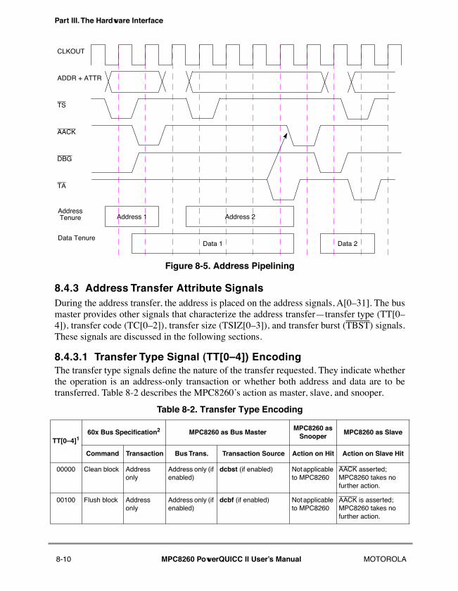
Part III. The Hardware Interface
Figure 8-5. Address Pipelining
8.4.3 Address Transfer Attribute SignalsDuring the address transfer, the address is placed on the address signals, A[0Ð31]. The busmaster provides other signals that characterize the address transferÑtransfer type (TT[0Ð4]), transfer code (TC[0Ð2]), transfer size (TSIZ[0Ð3]), and transfer burst (TBST) signals.These signals are discussed in the following sections.
8.4.3.1 Transfer Type Signal (TT[0Ð4]) EncodingThe transfer type signals deÞne the nature of the transfer requested. They indicate whetherthe operation is an address-only transaction or whether both address and data are to betransferred. Table 8-2 describes the MPC8260Õs action as master, slave, and snooper.
Table 8-2. Transfer Type Encoding
TT[0Ð4]160x Bus SpeciÞcation2 MPC8260 as Bus Master
MPC8260 as Snooper
MPC8260 as Slave
Command Transaction Bus Trans. Transaction Source Action on Hit Action on Slave Hit
00000 Clean block Address only
Address only (if enabled)
dcbst (if enabled) Not applicable to MPC8260
AACK asserted; MPC8260 takes no further action.
00100 Flush block Address only
Address only (if enabled)
dcbf (if enabled) Not applicable to MPC8260
AACK is asserted; MPC8260 takes no further action.
CLKOUT
ADDR + ATTR
TS
AACK
DBG
TA
Address
Data Tenure
Tenure Address 1
Data 1
Address 2
Data 2
8-10 MPC8260 PowerQUICC II UserÕs Manual MOTOROLA
Part III. The Hardware Interface
01000 sync Address only
Address only (if enabled)
sync (if enabled) Not applicable to MPC8260
Assert AACK. BG is negated until MPC8260 buffers are ßushed.
01100 Kill block Address only
Address only dcbz or dcbi (if enabled)
Flush, cancel reservation
AACK is asserted.
10000 eieio Address only
Address only (if enabled)
eieio (if enabled) Not applicable to MPC8260
Assert AACK. BG is negated until MPC8260 buffers are ßushed.
101 00 Graphics write
Single-beat write
Single-beat write (non-GLB)
ecowx Not applicable to MPC8260
No action.
11000 TLB invalidate
Address only
Not applicable to MPC8260
Not applicable to MPC8260
Not applicable to MPC8260
AACK is asserted; MPC8260 takes no further action.
11100 Graphics read
Single-beat read
Single-beat read (non-GBL)
eciwx Not applicable to MPC8260
MPC8260 takes no action.
00001 lwarx reservation set
Address only
Not applicable to MPC8260
Not applicable to MPC8260
Not applicable to MPC8260
Address-only operation. AACK is asserted; MPC8260 takes no further action.
00101 Reserved Ñ Not applicable to MPC8260
Not applicable to MPC8260
Not applicable to MPC8260
Illegal
01001 tlbsync Address only
Not applicable to MPC8260
Not applicable to MPC8260
Not applicable to MPC8260
Address-only operation. AACK is asserted; MPC8260 takes no further action.
01101 icbi Address only
Not applicable to MPC8260
Not applicable to MPC8260
Not applicable to MPC8260
Address-only operation. AACK is asserted; MPC8260 takes no further action.
1XX01 Reserved for customer
Ñ Not applicable to MPC8260
Not applicable to MPC8260
Not applicable to MPC8260
Illegal
00010 WR w/ßush Single-beat write or Burst
Single-beat write
CI, WT store, or non-processor master under
Flush, cancel reservation
Write, assert AACK and TA.
00110 WR w/Kill Burst Burst (non-GLB)
Castout, ca-op push, or snoop copyback
Kill, cancel reservation
Write, assert AACK and TA.
01010 Read Single-beat read or burst
Single-beat read
CI load, CI I-fetch or nonprocessor master
Clean or ßush Read, assert AACK and TA.
Table 8-2. Transfer Type Encoding (Continued)
TT[0Ð4]160x Bus SpeciÞcation2 MPC8260 as Bus Master
MPC8260 as Snooper
MPC8260 as Slave
Command Transaction Bus Trans. Transaction Source Action on Hit Action on Slave Hit
MOTOROLA Chapter 8. The 60x Bus 8-11
Part III. The Hardware Interface
Note the following regarding Table 8-2:
¥ For reads, the processor cleans or ßushes during a snoop based on the TBST input. The processor cleans for single-beat reads (TBST negated) to emulate read-with-no-intent-to-cache operations.
¥ Castouts and snoop copybacks are generally marked as non-global and are not snooped (except for reservation monitoring). However, other masters performing DMA write operations with the same TT encoding and marked as a global WR operation (whether global or non-global) will cancel an active reservation during a snoop hit in the reservation register (independent of a snoop hit in the cache).
¥ A non-processor read can cause the internal processor to invalidate the corresponding cache line if it exists.
01110 Read with intent to modify
Burst Burst Load miss, store miss, or I-fetch
Flush Read, assert AACK and TA.
10010 WR w/ßush atomic
Single-beat write
Single-beat write
stwcx Flush, cancel reservation
Write, assert AACK and TA
10110 Reserved Not applicable to MPC8260
Not applicable to MPC8260
Not applicable to MPC8260
Not applicable to MPC8260
Illegal
11010 Read atomic
Single-beat read or burst
Single-beat read
lwarx (CI load) Clean or ßush Read, assert AACK and TA
11110 Read with intent to modify atomic
Burst Burst lwarx (load miss) Flush Read, assert AACK and TA
00011 Reserved Ñ Not applicable to MPC8260
Not applicable to MPC8260
Not applicable to MPC8260
Illegal
00111 Reserved Ñ Not applicable to MPC8260
Not applicable to MPC8260
Not applicable to MPC8260
Illegal
01011 Read with no intent to cache
Single-beat read or burst
Not applicable to MPC8260
Not applicable to MPC8260
Clean Read, assert AACK and TA
01111 Reserved Ñ Not applicable to MPC8260
Not applicable to MPC8260
Not applicable to MPC8260
Illegal
1XX11 Reserved for customer
Ñ Not applicable to MPC8260
Not applicable to MPC8260
Not applicable to MPC8260
Illegal
1TT1 can be interpreted as a read-versus-write indicator for the bus.2This column speciÞes the TT encoding for the general 60x protocol. The processor generates or snoops only a
subset of those encodings.
Table 8-2. Transfer Type Encoding (Continued)
TT[0Ð4]160x Bus SpeciÞcation2 MPC8260 as Bus Master
MPC8260 as Snooper
MPC8260 as Slave
Command Transaction Bus Trans. Transaction Source Action on Hit Action on Slave Hit
8-12 MPC8260 PowerQUICC II UserÕs Manual MOTOROLA
Part III. The Hardware Interface
8.4.3.2 Transfer Code Signals TC[0Ð2] The transfer code signals, TC[0Ð2], provide supplemental information about thecorresponding address (mainly regarding the source of the transaction). Note that TCxsignals can be used with the TT[0Ð4] and TBST to further deÞne the current transaction.
8.4.3.3 TBST and TSIZ[0Ð3] Signals and Size of TransferAs shown in Table 8-4, the transfer size signals (TSIZ[0Ð3]) and the transfer burst signal(TBST) together indicate the size of the requested data transfer. These signals can be usedwith address bits A[27Ð31] and the device port size to determine which portion of the databus contains valid data for a write transaction or which portion of the bus should containvalid data for a read transaction.
The MPC8260 uses four double-word burst transactions for transferring cache blocks. Forthese transactions, TSIZ[0Ð3] are encoded as 0b0010, and address bits A[27Ð28] determinewhich double-word is sent Þrst.
The MPC8260 supports critical-word-Þrst burst transactions (double-word-aligned) fromthe processor. The MPC8260 transfers the critical double word of data Þrst, followed by thedouble words from increasing addresses, wrapping back to the beginning of the eight-wordblock as required.
Table 8-3 Transfer Code Encoding
TC[0Ð2] Read Write
000 Core data transaction Any write
001 Core touch load Ñ
010 Core instruction fetch Ñ
011 Reserved Ñ
100 Reserved
101 Reserved
110 DMA function code 0
111 DMA function code 1
Table 8-4. Transfer Size Signal Encoding
TBST TSIZ[0Ð3] Transfer Size Comments Source
Negated 0 0 0 1 1 Byte Byte Core and DMA
Negated 0 0 1 0 2 Bytes Half-word Core and DMA
Negated 0 0 1 1 3 Bytes Ñ Core and DMA
Negated 0 1 0 0 4 Bytes Word Core and DMA
Negated 0 1 0 1 5 Bytes Extended 5 bytes SDMA (MPC8260 only)
Negated 0 1 1 0 6 Bytes Extended 6 bytes SDMA (MPC8260 only)
MOTOROLA Chapter 8. The 60x Bus 8-13
Part III. The Hardware Interface
Note that the basic coherency size of the bus is 32 bytes for the processor (cache-blocksize). Data transfers that cross an aligned 32-byte boundary must present a new addressonto the bus at that boundary for proper snoop operation, or must operate as non-coherentwith respect to the MPC8260.
8.4.3.4 Burst Ordering During Data TransfersDuring burst transfers, 32 bytes of data (one cache block) are transferred to or from thecache. Burst write transfers are performed zero double-word-Þrst. However, because burstreads are performed critical-double-word-Þrst, a burst-read transfer may not start with theÞrst double word of the cache block and the cache-block-Þll operation may wrap aroundthe end of the cache block. Table 8-5 describes MPC8260 burst ordering.
Each data beat is terminated with an assertion of TA.
8.4.3.5 Effect of Alignment on Data TransfersTable 8-6 lists the aligned transfers that can occur to and from the MPC8260. These aretransfers in which the data is aligned to an address that is an integer multiple of the size ofthe data. For example, Table 8-6 shows that 1-byte data is always aligned; however, a 4-byteword must reside at an address that is a multiple of 4 to be aligned.
In Figure 8-6, Table 8-8, and Table 8-9, OP0 is the most-signiÞcant byte of a word operandand OP7 is the least-signiÞcant byte.
Negated 0 1 1 1 7 Bytes Extended 7 bytes SDMA (MPC8260 only)
Negated 0 0 0 0 8 Bytes Double-word (maximum data bus size) Core and DMA
Negated 1 0 0 1 16 Bytes Extended double double-word SDMA (MPC8260 only)
Negated 1 0 1 0 24 Bytes Extended triple double-word SDMA (MPC8260 only)
Asserted 0 0 1 0 32 bytes Quad double-word (4 maximum data beats) Core and DMA
Table 8-5. Burst Ordering
Data TransferDouble-Word Starting Address:
A[27Ð28] = 001
1A[27Ð28] speciÞes the Þrst double word of the 32-byte block being transferred; any subsequent double words must wrap-around the block. A[29Ð31] are always 0b000 for burst transfers by the MPC8260.
A[27Ð28] = 01 A[27Ð28] = 10 A[27Ð28] = 11
1st data beat DW02
2DWx represents the double word that would be addressed by A[27Ð28] = x if a nonburst transfer were performed.
DW1 DW2 DW3
2nd data beat DW1 DW2 DW3 DW0
3rd data beat DW2 DW3 DW0 DW1
4th data beat DW3 DW0 DW1 DW2
Table 8-4. Transfer Size Signal Encoding (Continued)
TBST TSIZ[0Ð3] Transfer Size Comments Source
8-14 MPC8260 PowerQUICC II UserÕs Manual MOTOROLA
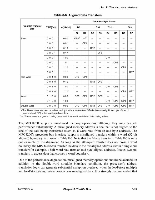
Part III. The Hardware Interface
The MPC8260 supports misaligned memory operations, although they may degradeperformance substantially. A misaligned memory address is one that is not aligned to thesize of the data being transferred (such as, a word read from an odd byte address). TheMPC8260Õs processor bus interface supports misaligned transfers within a word (32-bitaligned) boundary, as shown in Table 8-7. Note that the 4-byte transfer in Table 8-7 is onlyone example of misalignment. As long as the attempted transfer does not cross a wordboundary, the MPC8260 can transfer the data to the misaligned address within a single bustransfer (for example, a half-word read from an odd byte-aligned address). It takes two bustransfers to access data that crosses a word boundary.
Due to the performance degradation, misaligned memory operations should be avoided. Inaddition to the double-word straddle boundary condition, the processorÕs addresstranslation logic can generate substantial exception overhead when the load/store multipleand load/store string instructions access misaligned data. It is strongly recommended that
Table 8-6. Aligned Data Transfers
Program Transfer Size
TSIZ[0Ð3] A[29Ð31]
Data Bus Byte Lanes
D0... ...D31 D32... ...D63
B0 B1 B2 B3 B4 B5 B6 B7
Byte 0 0 0 1 0 0 0 OP01
1OPn: These lanes are read or written during that bus transaction. OP0 is the most-signiÞcant byte of a word operand and OP7 is the least-signiÞcant byte.
Ñ2
2Ñ: These lanes are ignored during reads and driven with undeÞned data during writes.
Ñ Ñ Ñ Ñ Ñ Ñ
0 0 0 1 0 0 1 Ñ OP1 Ñ Ñ Ñ Ñ Ñ Ñ
0 0 0 1 0 1 0 Ñ Ñ OP2 Ñ Ñ Ñ Ñ Ñ
0 0 0 1 0 1 1 Ñ Ñ Ñ OP3 Ñ Ñ Ñ Ñ
0 0 0 1 1 0 0 Ñ Ñ Ñ Ñ OP4 Ñ Ñ Ñ
0 0 0 1 1 0 1 Ñ Ñ Ñ Ñ Ñ OP5 Ñ Ñ
0 0 0 1 1 1 0 Ñ Ñ Ñ Ñ Ñ Ñ OP6 Ñ
0 0 0 1 1 1 1 Ñ Ñ Ñ Ñ Ñ Ñ Ñ OP7
Half-Word 0 0 1 0 0 0 0 OP0 OP1 Ñ Ñ Ñ Ñ Ñ Ñ
0 0 1 0 0 1 0 Ñ Ñ OP2 OP3 Ñ Ñ Ñ Ñ
0 0 1 0 1 0 0 Ñ Ñ Ñ Ñ OP4 OP5 Ñ Ñ
0 0 1 0 1 1 0 Ñ Ñ Ñ Ñ Ñ Ñ OP6 OP7
Word 0 1 0 0 0 0 0 OP0 OP1 OP2 OP3 Ñ Ñ Ñ Ñ
0 1 0 0 1 0 0 Ñ Ñ Ñ Ñ OP4 OP5 OP6 OP7
Double-Word 0 0 0 0 0 0 0 OP0 OP1 OP2 OP3 OP4 OP5 OP6 OP7
MOTOROLA Chapter 8. The 60x Bus 8-15
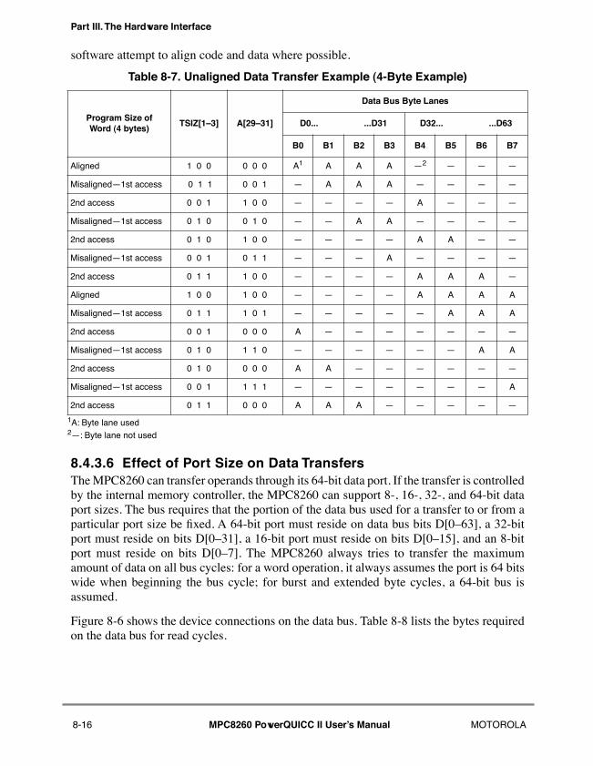
Part III. The Hardware Interface
software attempt to align code and data where possible.
8.4.3.6 Effect of Port Size on Data TransfersThe MPC8260 can transfer operands through its 64-bit data port. If the transfer is controlledby the internal memory controller, the MPC8260 can support 8-, 16-, 32-, and 64-bit dataport sizes. The bus requires that the portion of the data bus used for a transfer to or from aparticular port size be Þxed. A 64-bit port must reside on data bus bits D[0Ð63], a 32-bitport must reside on bits D[0Ð31], a 16-bit port must reside on bits D[0Ð15], and an 8-bitport must reside on bits D[0Ð7]. The MPC8260 always tries to transfer the maximumamount of data on all bus cycles: for a word operation, it always assumes the port is 64 bitswide when beginning the bus cycle; for burst and extended byte cycles, a 64-bit bus isassumed.
Figure 8-6 shows the device connections on the data bus. Table 8-8 lists the bytes requiredon the data bus for read cycles.
Table 8-7. Unaligned Data Transfer Example (4-Byte Example)
Program Size ofWord (4 bytes)
TSIZ[1Ð3] A[29Ð31]
Data Bus Byte Lanes
D0... ...D31 D32... ...D63
B0 B1 B2 B3 B4 B5 B6 B7
Aligned 1 0 0 0 0 0 A1
1A: Byte lane used
A A A Ñ2
2Ñ: Byte lane not used
Ñ Ñ Ñ
MisalignedÑ1st access 0 1 1 0 0 1 Ñ A A A Ñ Ñ Ñ Ñ
2nd access 0 0 1 1 0 0 Ñ Ñ Ñ Ñ A Ñ Ñ Ñ
MisalignedÑ1st access 0 1 0 0 1 0 Ñ Ñ A A Ñ Ñ Ñ Ñ
2nd access 0 1 0 1 0 0 Ñ Ñ Ñ Ñ A A Ñ Ñ
MisalignedÑ1st access 0 0 1 0 1 1 Ñ Ñ Ñ A Ñ Ñ Ñ Ñ
2nd access 0 1 1 1 0 0 Ñ Ñ Ñ Ñ A A A Ñ
Aligned 1 0 0 1 0 0 Ñ Ñ Ñ Ñ A A A A
MisalignedÑ1st access 0 1 1 1 0 1 Ñ Ñ Ñ Ñ Ñ A A A
2nd access 0 0 1 0 0 0 A Ñ Ñ Ñ Ñ Ñ Ñ Ñ
MisalignedÑ1st access 0 1 0 1 1 0 Ñ Ñ Ñ Ñ Ñ Ñ A A
2nd access 0 1 0 0 0 0 A A Ñ Ñ Ñ Ñ Ñ Ñ
MisalignedÑ1st access 0 0 1 1 1 1 Ñ Ñ Ñ Ñ Ñ Ñ Ñ A
2nd access 0 1 1 0 0 0 A A A Ñ Ñ Ñ Ñ Ñ
8-16 MPC8260 PowerQUICC II UserÕs Manual MOTOROLA
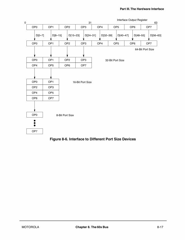
Part III. The Hardware Interface
Figure 8-6. Interface to Different Port Size Devices
0 31 63
OP0 OP1 OP2 OP3 OP4 OP5 OP6 OP7
OP0 OP1 OP2 OP3 OP4 OP5 OP6 OP7
D[0Ð7] D[8Ð15] D[15Ð23] D[24Ð31] D[32Ð39] D[40Ð47] D[48Ð55] D[56Ð63]
OP0 OP1 OP2 OP3
OP4 OP5 OP6 OP7
OP0 OP1
OP2 OP3
OP4 OP5
OP6 OP7
OP0
OP7
32-Bit Port Size
64-Bit Port Size
Interface Output Register
16-Bit Port Size
8-Bit Port Size
MOTOROLA Chapter 8. The 60x Bus 8-17
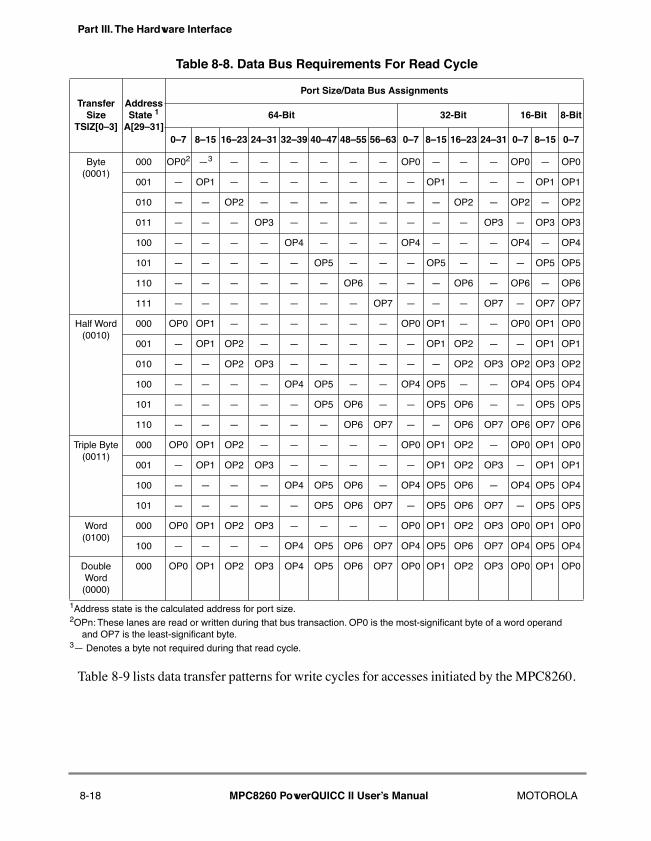
Part III. The Hardware Interface
Table 8-9 lists data transfer patterns for write cycles for accesses initiated by the MPC8260.
Table 8-8. Data Bus Requirements For Read Cycle
TransferSize
TSIZ[0Ð3]
Address State 1
A[29Ð31]
1Address state is the calculated address for port size.
Port Size/Data Bus Assignments
64-Bit 32-Bit 16-Bit 8-Bit
0Ð7 8Ð15 16Ð23 24Ð31 32Ð39 40Ð47 48Ð55 56Ð63 0Ð7 8Ð15 16Ð23 24Ð31 0Ð7 8Ð15 0Ð7
Byte(0001)
000 OP02
2OPn: These lanes are read or written during that bus transaction. OP0 is the most-signiÞcant byte of a word operand and OP7 is the least-signiÞcant byte.
Ñ3
3Ñ Denotes a byte not required during that read cycle.
Ñ Ñ Ñ Ñ Ñ Ñ OP0 Ñ Ñ Ñ OP0 Ñ OP0
001 Ñ OP1 Ñ Ñ Ñ Ñ Ñ Ñ Ñ OP1 Ñ Ñ Ñ OP1 OP1
010 Ñ Ñ OP2 Ñ Ñ Ñ Ñ Ñ Ñ Ñ OP2 Ñ OP2 Ñ OP2
011 Ñ Ñ Ñ OP3 Ñ Ñ Ñ Ñ Ñ Ñ Ñ OP3 Ñ OP3 OP3
100 Ñ Ñ Ñ Ñ OP4 Ñ Ñ Ñ OP4 Ñ Ñ Ñ OP4 Ñ OP4
101 Ñ Ñ Ñ Ñ Ñ OP5 Ñ Ñ Ñ OP5 Ñ Ñ Ñ OP5 OP5
110 Ñ Ñ Ñ Ñ Ñ Ñ OP6 Ñ Ñ Ñ OP6 Ñ OP6 Ñ OP6
111 Ñ Ñ Ñ Ñ Ñ Ñ Ñ OP7 Ñ Ñ Ñ OP7 Ñ OP7 OP7
Half Word(0010)
000 OP0 OP1 Ñ Ñ Ñ Ñ Ñ Ñ OP0 OP1 Ñ Ñ OP0 OP1 OP0
001 Ñ OP1 OP2 Ñ Ñ Ñ Ñ Ñ Ñ OP1 OP2 Ñ Ñ OP1 OP1
010 Ñ Ñ OP2 OP3 Ñ Ñ Ñ Ñ Ñ Ñ OP2 OP3 OP2 OP3 OP2
100 Ñ Ñ Ñ Ñ OP4 OP5 Ñ Ñ OP4 OP5 Ñ Ñ OP4 OP5 OP4
101 Ñ Ñ Ñ Ñ Ñ OP5 OP6 Ñ Ñ OP5 OP6 Ñ Ñ OP5 OP5
110 Ñ Ñ Ñ Ñ Ñ Ñ OP6 OP7 Ñ Ñ OP6 OP7 OP6 OP7 OP6
Triple Byte (0011)
000 OP0 OP1 OP2 Ñ Ñ Ñ Ñ Ñ OP0 OP1 OP2 Ñ OP0 OP1 OP0
001 Ñ OP1 OP2 OP3 Ñ Ñ Ñ Ñ Ñ OP1 OP2 OP3 Ñ OP1 OP1
100 Ñ Ñ Ñ Ñ OP4 OP5 OP6 Ñ OP4 OP5 OP6 Ñ OP4 OP5 OP4
101 Ñ Ñ Ñ Ñ Ñ OP5 OP6 OP7 Ñ OP5 OP6 OP7 Ñ OP5 OP5
Word(0100)
000 OP0 OP1 OP2 OP3 Ñ Ñ Ñ Ñ OP0 OP1 OP2 OP3 OP0 OP1 OP0
100 Ñ Ñ Ñ Ñ OP4 OP5 OP6 OP7 OP4 OP5 OP6 OP7 OP4 OP5 OP4
Double Word(0000)
000 OP0 OP1 OP2 OP3 OP4 OP5 OP6 OP7 OP0 OP1 OP2 OP3 OP0 OP1 OP0
8-18 MPC8260 PowerQUICC II UserÕs Manual MOTOROLA
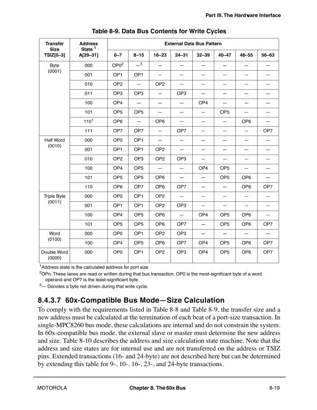
Part III. The Hardware Interface
8.4.3.7 60x-Compatible Bus ModeÑSize CalculationTo comply with the requirements listed in Table 8-8 and Table 8-9, the transfer size and anew address must be calculated at the termination of each beat of a port-size transaction. Insingle-MPC8260 bus mode, these calculations are internal and do not constrain the system.In 60x-compatible bus mode, the external slave or master must determine the new addressand size. Table 8-10 describes the address and size calculation state machine. Note that theaddress and size states are for internal use and are not transferred on the address or TSIZpins. Extended transactions (16- and 24-byte) are not described here but can be determinedby extending this table for 9-, 10-, 16-, 23-, and 24-byte transactions.
Table 8-9. Data Bus Contents for Write Cycles
TransferSize
TSIZ[0Ð3]
AddressState 1
A[29Ð31]
1Address state is the calculated address for port size
External Data Bus Pattern
0Ð7 8Ð15 16Ð23 24Ð31 32Ð39 40Ð47 48Ð55 56Ð63
Byte(0001)
000 OP02
2OPn: These lanes are read or written during that bus transaction. OP0 is the most-signiÞcant byte of a word operand and OP7 is the least-signiÞcant byte.
Ñ3
3Ñ Denotes a byte not driven during that write cycle.
Ñ Ñ Ñ Ñ Ñ Ñ
001 OP1 OP1 Ñ Ñ Ñ Ñ Ñ Ñ
010 OP2 Ñ OP2 Ñ Ñ Ñ Ñ Ñ
011 OP3 OP3 Ñ OP3 Ñ Ñ Ñ Ñ
100 OP4 Ñ Ñ Ñ OP4 Ñ Ñ Ñ
101 OP5 OP5 Ñ Ñ Ñ OP5 Ñ Ñ
1101 OP6 Ñ OP6 Ñ Ñ Ñ OP6 Ñ
111 OP7 OP7 Ñ OP7 Ñ Ñ Ñ OP7
Half Word(0010)
000 OP0 OP1 Ñ Ñ Ñ Ñ Ñ Ñ
001 OP1 OP1 OP2 Ñ Ñ Ñ Ñ Ñ
010 OP2 OP3 OP2 OP3 Ñ Ñ Ñ Ñ
100 OP4 OP5 Ñ Ñ OP4 OP5 Ñ Ñ
101 OP5 OP5 OP6 Ñ Ñ OP5 OP6 Ñ
110 OP6 OP7 OP6 OP7 Ñ Ñ OP6 OP7
Triple Byte (0011)
000 OP0 OP1 OP2 Ñ Ñ Ñ Ñ Ñ
001 OP1 OP1 OP2 OP3 Ñ Ñ Ñ Ñ
100 OP4 OP5 OP6 Ñ OP4 OP5 OP6 Ñ
101 OP5 OP5 OP6 OP7 Ñ OP5 OP6 OP7
Word(0100)
000 OP0 OP1 OP2 OP3 Ñ Ñ Ñ Ñ
100 OP4 OP5 OP6 OP7 OP4 OP5 OP6 OP7
Double Word(0000)
000 OP0 OP1 OP2 OP3 OP4 OP5 OP6 OP7
MOTOROLA Chapter 8. The 60x Bus 8-19
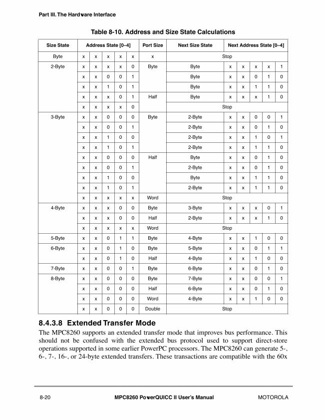
Part III. The Hardware Interface
8.4.3.8 Extended Transfer ModeThe MPC8260 supports an extended transfer mode that improves bus performance. Thisshould not be confused with the extended bus protocol used to support direct-storeoperations supported in some earlier PowerPC processors. The MPC8260 can generate 5-,6-, 7-, 16-, or 24-byte extended transfers. These transactions are compatible with the 60x
Table 8-10. Address and Size State Calculations
Size State Address State [0Ð4] Port Size Next Size State Next Address State [0Ð4]
Byte x x x x x x Stop
2-Byte x x x x 0 Byte Byte x x x x 1
x x 0 0 1 Byte x x 0 1 0
x x 1 0 1 Byte x x 1 1 0
x x x 0 1 Half Byte x x x 1 0
x x x x 0 Stop
3-Byte x x 0 0 0 Byte 2-Byte x x 0 0 1
x x 0 0 1 2-Byte x x 0 1 0
x x 1 0 0 2-Byte x x 1 0 1
x x 1 0 1 2-Byte x x 1 1 0
x x 0 0 0 Half Byte x x 0 1 0
x x 0 0 1 2-Byte x x 0 1 0
x x 1 0 0 Byte x x 1 1 0
x x 1 0 1 2-Byte x x 1 1 0
x x x x x Word Stop
4-Byte x x x 0 0 Byte 3-Byte x x x 0 1
x x x 0 0 Half 2-Byte x x x 1 0
x x x x x Word Stop
5-Byte x x 0 1 1 Byte 4-Byte x x 1 0 0
6-Byte x x 0 1 0 Byte 5-Byte x x 0 1 1
x x 0 1 0 Half 4-Byte x x 1 0 0
7-Byte x x 0 0 1 Byte 6-Byte x x 0 1 0
8-Byte x x 0 0 0 Byte 7-Byte x x 0 0 1
x x 0 0 0 Half 6-Byte x x 0 1 0
x x 0 0 0 Word 4-Byte x x 1 0 0
x x 0 0 0 Double Stop
8-20 MPC8260 PowerQUICC II UserÕs Manual MOTOROLA

Part III. The Hardware Interface
bus, but some slaves or masters do not support these features. Clear BCR[ETM] to disablethis type of transaction. This places the MPC8260 in strict 60x bus mode. The followingtables are extensions to Table 8-9, Table 8-8, and Table 8-10.
Table 8-11 lists the patterns of the extended data transfer for write cycles when MPC8260initiates an access. Note that 16- and 24-byte transfers are always eight-byte aligned anduse a 64-bit or less port size.
Table 8-12 lists the bytes required on the data bus for extended read cycles. Note that 16-and 24-byte transfers are always 8-byte aligned and use a maximum 64-bit port size.
Table 8-13 includes added states to the transfer size calculation state machine. Onlyextended transfers use these states.
Table 8-11. Data Bus Contents for Extended Write Cycles
Transfer Size
TSIZ[0Ð3])
Address State A[29Ð
31]
External Data Bus Pattern
D[0Ð7] D[8Ð15] D[16Ð23] D[24Ð31] D[32Ð39] D[40Ð47] D[48Ð55] D[56Ð63]
5 Bytes(0101)
000 OP0 OP1 OP2 OP3 OP4 Ñ Ñ Ñ
011 OP3 OP3 Ñ OP3 OP4 OP5 OP6 OP7
6 Bytes(0110)
000 OP0 OP1 OP2 OP3 OP4 OP5 Ñ Ñ
010 OP2 OP3 OP2 OP3 OP4 OP5 OP6 OP7
7 Bytes(0111)
000 OP0 OP1 OP2 OP3 OP4 OP5 OP6 Ñ
001 OP1 OP1 OP2 OP3 OP4 OP5 OP6 OP7
Table 8-12. Data Bus Requirements for Extended Read Cycles
Transfer Size
TSIZ[0Ð3]
Address State
A[29-31]
Port Size/Data Bus Assignments
64-Bit 32-Bit 16-Bit 8-Bit
0Ð7 8Ð15 16Ð23 24Ð31 32Ð39 40Ð47 48Ð55 56Ð63 0Ð7 8Ð15 16Ð23 24Ð31 0Ð7 8Ð15 0Ð7
5 Byte(0101)
000 OP0 OP1 OP2 OP3 OP4 Ñ Ñ Ñ OP0 OP1 OP2 OP3 OP0 OP1 OP0
011 Ñ Ñ Ñ OP3 OP4 OP5 OP6 OP7 Ñ Ñ Ñ OP3 Ñ OP3 OP3
6 Byte(0110)
000 OP0 OP1 OP2 OP3 OP4 OP5 Ñ Ñ OP0 OP1 OP2 OP3 OP0 OP1 OP0
010 Ñ Ñ OP2 OP3 OP4 OP5 OP6 OP7 Ñ Ñ OP2 OP3 OP2 OP3 OP2
7 Byte(0111)
000 OP0 OP1 OP2 OP3 OP4 OP5 OP6 Ñ OP0 OP1 OP2 OP3 OP0 OP1 OP0
001 Ñ OP1 OP2 OP3 OP4 OP5 OP6 OP7 Ñ OP1 OP2 OP3 Ñ OP1 OP1
MOTOROLA Chapter 8. The 60x Bus 8-21
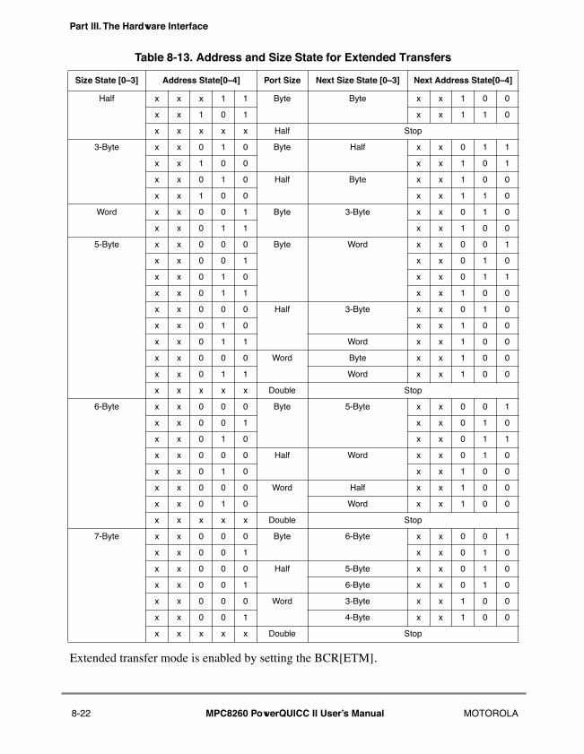
Part III. The Hardware Interface
Extended transfer mode is enabled by setting the BCR[ETM].
Table 8-13. Address and Size State for Extended Transfers
Size State [0Ð3] Address State[0Ð4] Port Size Next Size State [0Ð3] Next Address State[0Ð4]
Half x x x 1 1 Byte Byte x x 1 0 0
x x 1 0 1 x x 1 1 0
x x x x x Half Stop
3-Byte x x 0 1 0 Byte Half x x 0 1 1
x x 1 0 0 x x 1 0 1
x x 0 1 0 Half Byte x x 1 0 0
x x 1 0 0 x x 1 1 0
Word x x 0 0 1 Byte 3-Byte x x 0 1 0
x x 0 1 1 x x 1 0 0
5-Byte x x 0 0 0 Byte Word x x 0 0 1
x x 0 0 1 x x 0 1 0
x x 0 1 0 x x 0 1 1
x x 0 1 1 x x 1 0 0
x x 0 0 0 Half 3-Byte x x 0 1 0
x x 0 1 0 x x 1 0 0
x x 0 1 1 Word x x 1 0 0
x x 0 0 0 Word Byte x x 1 0 0
x x 0 1 1 Word x x 1 0 0
x x x x x Double Stop
6-Byte x x 0 0 0 Byte 5-Byte x x 0 0 1
x x 0 0 1 x x 0 1 0
x x 0 1 0 x x 0 1 1
x x 0 0 0 Half Word x x 0 1 0
x x 0 1 0 x x 1 0 0
x x 0 0 0 Word Half x x 1 0 0
x x 0 1 0 Word x x 1 0 0
x x x x x Double Stop
7-Byte x x 0 0 0 Byte 6-Byte x x 0 0 1
x x 0 0 1 x x 0 1 0
x x 0 0 0 Half 5-Byte x x 0 1 0
x x 0 0 1 6-Byte x x 0 1 0
x x 0 0 0 Word 3-Byte x x 1 0 0
x x 0 0 1 4-Byte x x 1 0 0
x x x x x Double Stop
8-22 MPC8260 PowerQUICC II UserÕs Manual MOTOROLA
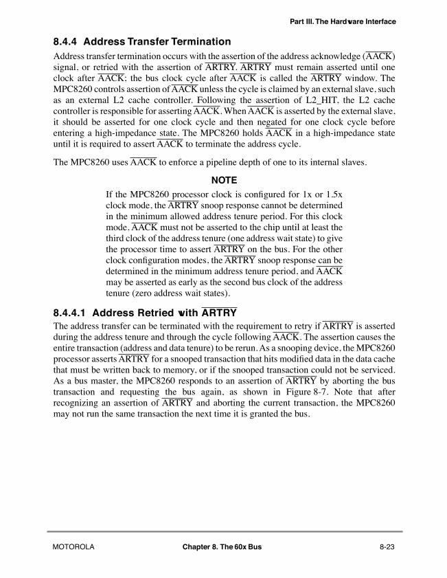
Part III. The Hardware Interface
8.4.4 Address Transfer TerminationAddress transfer termination occurs with the assertion of the address acknowledge (AACK)signal, or retried with the assertion of ARTRY. ARTRY must remain asserted until oneclock after AACK; the bus clock cycle after AACK is called the ARTRY window. TheMPC8260 controls assertion of AACK unless the cycle is claimed by an external slave, suchas an external L2 cache controller. Following the assertion of L2_HIT, the L2 cachecontroller is responsible for asserting AACK. When AACK is asserted by the external slave,it should be asserted for one clock cycle and then negated for one clock cycle beforeentering a high-impedance state. The MPC8260 holds AACK in a high-impedance stateuntil it is required to assert AACK to terminate the address cycle.
The MPC8260 uses AACK to enforce a pipeline depth of one to its internal slaves.
NOTEIf the MPC8260 processor clock is conÞgured for 1x or 1.5xclock mode, the ARTRY snoop response cannot be determinedin the minimum allowed address tenure period. For this clockmode, AACK must not be asserted to the chip until at least thethird clock of the address tenure (one address wait state) to givethe processor time to assert ARTRY on the bus. For the otherclock conÞguration modes, the ARTRY snoop response can bedetermined in the minimum address tenure period, and AACKmay be asserted as early as the second bus clock of the addresstenure (zero address wait states).
8.4.4.1 Address Retried with ARTRYThe address transfer can be terminated with the requirement to retry if ARTRY is assertedduring the address tenure and through the cycle following AACK. The assertion causes theentire transaction (address and data tenure) to be rerun. As a snooping device, the MPC8260processor asserts ARTRY for a snooped transaction that hits modiÞed data in the data cachethat must be written back to memory, or if the snooped transaction could not be serviced.As a bus master, the MPC8260 responds to an assertion of ARTRY by aborting the bustransaction and requesting the bus again, as shown in Figure 8-7. Note that afterrecognizing an assertion of ARTRY and aborting the current transaction, the MPC8260may not run the same transaction the next time it is granted the bus.
MOTOROLA Chapter 8. The 60x Bus 8-23
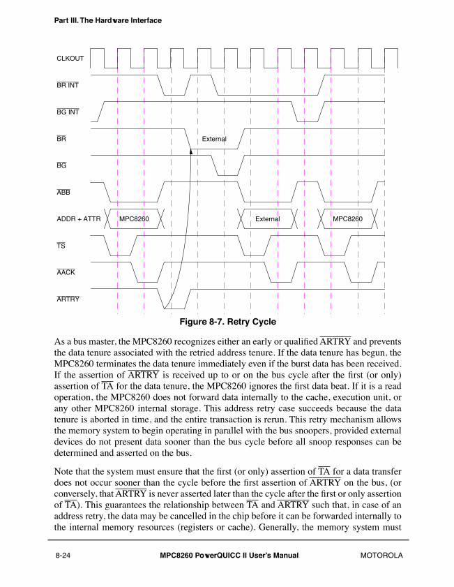
Part III. The Hardware Interface
Figure 8-7. Retry Cycle
As a bus master, the MPC8260 recognizes either an early or qualiÞed ARTRY and preventsthe data tenure associated with the retried address tenure. If the data tenure has begun, theMPC8260 terminates the data tenure immediately even if the burst data has been received.If the assertion of ARTRY is received up to or on the bus cycle after the Þrst (or only)assertion of TA for the data tenure, the MPC8260 ignores the Þrst data beat. If it is a readoperation, the MPC8260 does not forward data internally to the cache, execution unit, orany other MPC8260 internal storage. This address retry case succeeds because the datatenure is aborted in time, and the entire transaction is rerun. This retry mechanism allowsthe memory system to begin operating in parallel with the bus snoopers, provided externaldevices do not present data sooner than the bus cycle before all snoop responses can bedetermined and asserted on the bus.
Note that the system must ensure that the Þrst (or only) assertion of TA for a data transferdoes not occur sooner than the cycle before the Þrst assertion of ARTRY on the bus, (orconversely, that ARTRY is never asserted later than the cycle after the Þrst or only assertionof TA). This guarantees the relationship between TA and ARTRY such that, in case of anaddress retry, the data may be cancelled in the chip before it can be forwarded internally tothe internal memory resources (registers or cache). Generally, the memory system must
CLKOUT
BR INT
BG
ADDR + ATTR
BG INT
BR
ABB
TS
AACK
ARTRY
MPC8260 External MPC8260
External
8-24 MPC8260 PowerQUICC II UserÕs Manual MOTOROLA
Part III. The Hardware Interface
also detect this event and abort any transfer in progress. If this TA/ARTRY relationship isnot met, the master may enter an undeÞned state. Users may use PPC_ACR[DBGD] toensure correct operation of the system.
During the clock of a qualiÞed ARTRY, each device master determines whether it shouldnegate BR and ignore BG on the following cycle. The following cycle is referred to as thewindow-of-opportunity for the snooping master. During this window, only the snoopingmaster that asserted ARTRY and requires a snoop copyback operation is allowed to assertBR. This guarantees the snooping master a window of opportunity to request and be grantedthe bus before the just-retried master can restart its transaction. BG is also blocked in thewindow-of-opportunity, so the arbiter has a chance to negate BG to an already grantedpotential bus master to perform a new arbitration.
Note that in some systems, an external processor may be unable to perform a pending snoopcopyback when a new snoop operation is performed. In this case, the MPC8260 requeststhe window of opportunity if it hits on the new snooped address. To clear its internal snoopqueue, it performs the snoop copyback operation for the earlier snooped address instead ofthe current snooped address.
8.4.4.2 Address Tenure Timing ConÞgurationDuring address tenures initiated by 60x-bus devices, the timing of the assertion of AACKby the MPC8260 is determined by the BCR[APD] and the pipeline status of the 60x bus.Because the MPC8260 can support one level of pipelining, it uses AACK to control the60x-bus pipeline condition. To maintain the one-level pipeline, AACK is not asserted for apipelined address tenure until the current data tenure ends. The MPC8260 also delaysasserting AACK until no more address retry conditions can occur. Note that the earliest theMPC8260 can assert AACK is the clock cycle when the wait-state values set by BCR[APD]have expired.
BCR[APD] speciÞes the minimum number of address tenure wait states for addressoperations initiated by 60x-bus devices. APD indicates how many cycles the MPC8260should wait for ARTRY, but because it is assumed that ARTRY can be asserted (by othermasters) only on cacheable address spaces, APD is considered only on transactions that hita 60x-assigned memory controller bank and that have GBL asserted during the addressphase.
Extra wait states may occur because of other MPC8260 conÞguration parameters. Note thatin a system with an L2 cache, the number of wait states conÞgured by BCR[APD] shouldbe at least as large as the value needed by the L2 controller to assert hit response. In systemswith multiple potential masters, the number of wait states conÞgured by BCR[APD] shouldbe at least as large as the value the slowest master would need by to assert a snoop response.For example, additional wait states are required when the internal processor is in 1:1 clockmode; this case requires at least one wait state to generate the ARTRY response.
MOTOROLA Chapter 8. The 60x Bus 8-25
Part III. The Hardware Interface
8.4.5 Pipeline ControlThe MPC8260 supports the two following modes:
¥ One-level pipeline modeÑTo maintain the one-level pipeline, AACK is not asserted for a pipelined address tenure until the current data tenure ends. In 60x-compatible bus mode, a two-level pipeline depth can occur (for example, when an external 60x-bus slave does not support one-level pipelining). When the internal arbiter counts a pipeline depth of two (two assertions of AACK before the assertion of the current data tenure) it negates all address bus grant (BG) signals.
¥ No-pipeline modeÑThe MPC8260 does not assert AACK until the corresponding data tenure ends.
8.5 Data Tenure OperationsThis section describes the operation of the MPC8260 during the data bus arbitration,transfer, and termination phases of the data tenure.
8.5.1 Data Bus ArbitrationThe beginning of an address transfer, marked by the assertion of transfer start (TS), is alsoan implicit data bus request provided that the transfer type signals (TT[0Ð4]) indicate thatthe transaction is not address-only.
The MPC8260 arbiter supports one external master and uses DBG to grant the externalmaster data bus.The DBG signals are not asserted if the data bus, which is shared withmemory, is busy with a transaction.
A qualiÞed data bus grant (QDBG) can be expressed as the assertion of DBG while DBBand ARTRY (associated with the data bus operation) are negated.
Note that the MPC8260 arbiter should assert DBG only when it is certain that the Þrst TAwill be asserted with or after the associated ARTRY. The MPC8260 DBG is asserted withTS if the data bus is free and if the PPC_ACR[DBGD] = 0. If PPC_ACR[DBGD] = 1, DBGis asserted one cycle after TS if the data bus is not busy. The DBG delay should be used toensure that ARTRY is not asserted after the Þrst or only TA assertion. For the programmingmodel, see Section 4.3.2.2, Ò60x Bus Arbiter ConÞguration Register (PPC_ACR).Ó
Note that DBB should not be asserted after the data tenure is Þnished. Assertion of DBBafter the last TA causes improper operation of the bus. (MPC8260 internal masters do notassert DBB after the last TA.)
Note the following:
¥ External bus arbiters must comply with the following restriction on assertion of DBG which is connected to the MPC8260. In case the data bus is not busy with the data of a previous transaction on the bus, external arbiter must assert DBG in the same cycle in which TS is asserted (by a master which was granted the bus) or in the
8-26 MPC8260 PowerQUICC II UserÕs Manual MOTOROLA
Part III. The Hardware Interface
following cycle. In case the external arbiter asserts DBG on the cycle in which TS was asserted, PPC_ACR[DBGD] should be zero. Otherwise, PPC_ACR[DBGD] should be set.
¥ External masters connected to the 60x bus must assert DBB only for the duration of its data tenure. External masters should not use DBB to prevent other masters from using the data bus after their data tenure has ended.
8.5.2 Data Streaming ModeThe MPC8260 supports a special data streaming mode that can improve bus performancein some conditions. Generally, the bus protocol requires one idle cycle between any twodata tenures. This idle cycle is essential to prevent contention on the data bus when thedriver of the data is changing. However, when the driver on the data bus is the same for bothdata tenures, this idle cycle may be omitted.
In data streaming mode, the MPC8260 omits the idle cycle where possible. MPC8260applications often require data stream transfers of more than 4 x 64 bits. For example, theATM cellÕs payload is 6 x 64 bits. All this data is driven from a single device on the bus, sodata-streaming saves a cycle for such a transfer. When data-streaming mode is enabled,transactions initiated by the core are not affected, while transactions initiated by other busmasters within the chip omit the idle cycle if the data driver is the same. Note that datastreaming mode cannot be enabled when the MPC8260 is in 60x-compatible bus mode anda device that uses DBB is connected to the bus. This restriction is due to the fact that aMPC8260 for which data streaming mode is enabled may leave DBB asserted after the lastTA of a transaction and this is a violation of the strict bus protocol. The data streamingmode is enabled by setting BCR[ETM].
8.5.3 Data Bus Transfers and Normal TerminationThe data transfer signals include D[0Ð63] and DP[0Ð7]. For memory accesses, the datasignals form a 64-bit data path, D[0Ð63], for read and write operations.
The MPC8260 handles data transfers in either single-beat or burst operations. Single-beatoperations can transfer from 1 to 24 bytes of data at a time. Burst operations always transfereight words in four double-word beats. A burst transaction is indicated by the assertion ofTBST by the bus master. A transaction is terminated normally by asserting TA.
The three following signals are used to terminate the individual data beats of the data tenureand the data tenure itself:
¥ TA indicates normal termination of data transactions. It must always be asserted on the bus cycle coincident with the data that it is qualifying. It may be withheld by the slave for any number of clocks until valid data is ready to be supplied or accepted.
¥ Asserting TEA indicates a nonrecoverable bus error event. Upon receiving a Þnal (or only) termination condition, the MPC8260 always negates DBB for one cycle, except when fast data bus grant is performed.
MOTOROLA Chapter 8. The 60x Bus 8-27
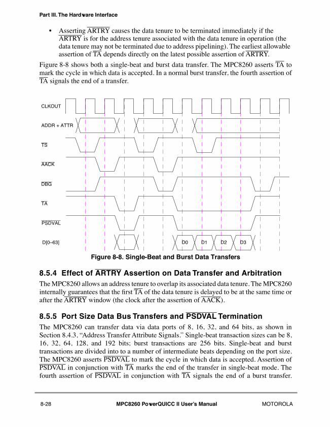
Part III. The Hardware Interface
¥ Asserting ARTRY causes the data tenure to be terminated immediately if the ARTRY is for the address tenure associated with the data tenure in operation (the data tenure may not be terminated due to address pipelining). The earliest allowable assertion of TA depends directly on the latest possible assertion of ARTRY.
Figure 8-8 shows both a single-beat and burst data transfer. The MPC8260 asserts TA tomark the cycle in which data is accepted. In a normal burst transfer, the fourth assertion ofTA signals the end of a transfer.
Figure 8-8. Single-Beat and Burst Data Transfers
8.5.4 Effect of ARTRY Assertion on Data Transfer and ArbitrationThe MPC8260 allows an address tenure to overlap its associated data tenure. The MPC8260internally guarantees that the Þrst TA of the data tenure is delayed to be at the same time orafter the ARTRY window (the clock after the assertion of AACK).
8.5.5 Port Size Data Bus Transfers and PSDVAL TerminationThe MPC8260 can transfer data via data ports of 8, 16, 32, and 64 bits, as shown inSection 8.4.3, ÒAddress Transfer Attribute Signals.Ó Single-beat transaction sizes can be 8,16, 32, 64, 128, and 192 bits; burst transactions are 256 bits. Single-beat and bursttransactions are divided into to a number of intermediate beats depending on the port size.The MPC8260 asserts PSDVAL to mark the cycle in which data is accepted. Assertion ofPSDVAL in conjunction with TA marks the end of the transfer in single-beat mode. Thefourth assertion of PSDVAL in conjunction with TA signals the end of a burst transfer.
CLKOUT
ADDR + ATTR
TS
AACK
DBG
TA
D[0Ð63]
PSDVAL
D0 D1 D2 D3
8-28 MPC8260 PowerQUICC II UserÕs Manual MOTOROLA

Part III. The Hardware Interface
Figure 8-9 shows an extended transaction of 4 words to a port size of 32 bits. The single-beat transaction is translated to four port-sized beats.
Figure 8-9. 128-Bit Extended Transfer to 32-Bit Port Size
Figure 8-10 shows a burst transfer to a 32-bit port. Each double-word burst beat is dividedinto two port-sized beats such that the four double words are transferred in eight beats.
CLKOUT
ADDR + ATTR
TS
AACK
DBG
PSDVAL
D[0Ð31]
TA
D0 D1 D2 D3
MOTOROLA Chapter 8. The 60x Bus 8-29
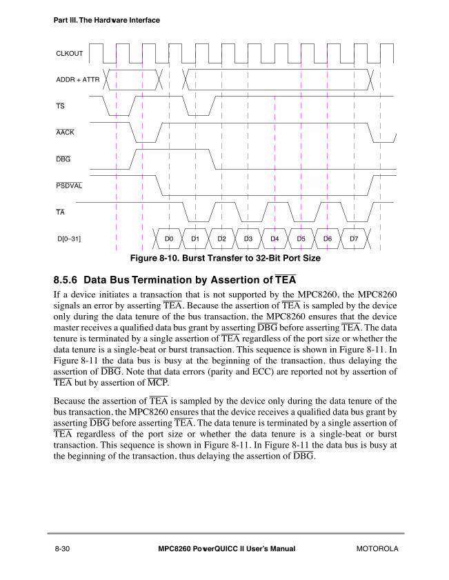
Part III. The Hardware Interface
Figure 8-10. Burst Transfer to 32-Bit Port Size
8.5.6 Data Bus Termination by Assertion of TEAIf a device initiates a transaction that is not supported by the MPC8260, the MPC8260signals an error by asserting TEA. Because the assertion of TEA is sampled by the deviceonly during the data tenure of the bus transaction, the MPC8260 ensures that the devicemaster receives a qualiÞed data bus grant by asserting DBG before asserting TEA. The datatenure is terminated by a single assertion of TEA regardless of the port size or whether thedata tenure is a single-beat or burst transaction. This sequence is shown in Figure 8-11. InFigure 8-11 the data bus is busy at the beginning of the transaction, thus delaying theassertion of DBG. Note that data errors (parity and ECC) are reported not by assertion ofTEA but by assertion of MCP.
Because the assertion of TEA is sampled by the device only during the data tenure of thebus transaction, the MPC8260 ensures that the device receives a qualiÞed data bus grant byasserting DBG before asserting TEA. The data tenure is terminated by a single assertion ofTEA regardless of the port size or whether the data tenure is a single-beat or bursttransaction. This sequence is shown in Figure 8-11. In Figure 8-11 the data bus is busy atthe beginning of the transaction, thus delaying the assertion of DBG.
CLKOUT
ADDR + ATTR
TS
AACK
DBG
PSDVAL
D[0Ð31]
TA
D0 D1 D2 D3 D4 D5 D6 D7
8-30 MPC8260 PowerQUICC II UserÕs Manual MOTOROLA
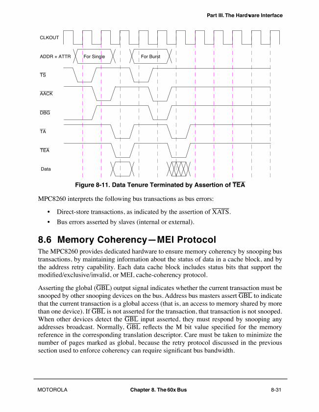
Part III. The Hardware Interface
Figure 8-11. Data Tenure Terminated by Assertion of TEA
MPC8260 interprets the following bus transactions as bus errors:
¥ Direct-store transactions, as indicated by the assertion of XATS.
¥ Bus errors asserted by slaves (internal or external).
8.6 Memory CoherencyÑMEI ProtocolThe MPC8260 provides dedicated hardware to ensure memory coherency by snooping bustransactions, by maintaining information about the status of data in a cache block, and bythe address retry capability. Each data cache block includes status bits that support themodiÞed/exclusive/invalid, or MEI, cache-coherency protocol.
Asserting the global (GBL) output signal indicates whether the current transaction must besnooped by other snooping devices on the bus. Address bus masters assert GBL to indicatethat the current transaction is a global access (that is, an access to memory shared by morethan one device). If GBL is not asserted for the transaction, that transaction is not snooped.When other devices detect the GBL input asserted, they must respond by snooping anyaddresses broadcast. Normally, GBL reßects the M bit value speciÞed for the memoryreference in the corresponding translation descriptor. Care must be taken to minimize thenumber of pages marked as global, because the retry protocol discussed in the previoussection used to enforce coherency can require signiÞcant bus bandwidth.
CLKOUT
ADDR + ATTR
TS
AACK
DBG
TA
Data
TEA
For Single For Burst
MOTOROLA Chapter 8. The 60x Bus 8-31
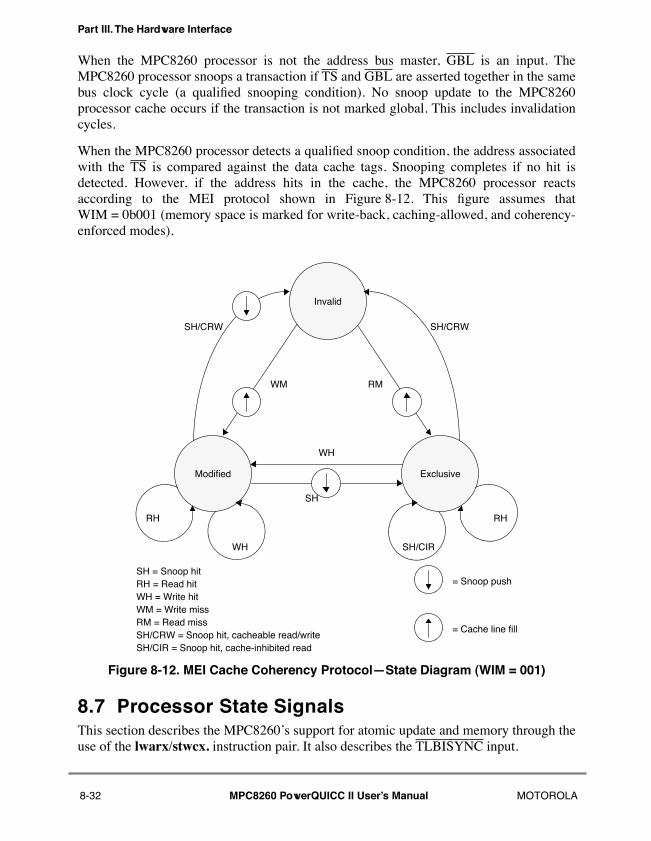
Part III. The Hardware Interface
When the MPC8260 processor is not the address bus master, GBL is an input. TheMPC8260 processor snoops a transaction if TS and GBL are asserted together in the samebus clock cycle (a qualiÞed snooping condition). No snoop update to the MPC8260processor cache occurs if the transaction is not marked global. This includes invalidationcycles.
When the MPC8260 processor detects a qualiÞed snoop condition, the address associatedwith the TS is compared against the data cache tags. Snooping completes if no hit isdetected. However, if the address hits in the cache, the MPC8260 processor reactsaccording to the MEI protocol shown in Figure 8-12. This Þgure assumes thatWIM = 0b001 (memory space is marked for write-back, caching-allowed, and coherency-enforced modes).
Figure 8-12. MEI Cache Coherency ProtocolÑState Diagram (WIM = 001)
8.7 Processor State SignalsThis section describes the MPC8260Õs support for atomic update and memory through theuse of the lwarx/stwcx. instruction pair. It also describes the TLBISYNC input.
Invalid
Modified
WH
SH
SH/CRW
WM
WH
RH
SH = Snoop hitRH = Read hitWH = Write hitWM = Write missRM = Read missSH/CRW = Snoop hit, cacheable read/writeSH/CIR = Snoop hit, cache-inhibited read
= Snoop push
= Cache line fill
Exclusive
SH/CRW
RM
SH/CIR
RH
8-32 MPC8260 PowerQUICC II UserÕs Manual MOTOROLA
Part III. The Hardware Interface
8.7.1 Support for the lwarx/stwcx. Instruction PairThe load word and reserve indexed (lwarx) and the store word conditional indexed (stwcx.)instructions provide a way to update memory atomically by setting a reservation on the loadand checking that the reservation is still valid before the store is performed. In theMPC8260, reservations are made on behalf of aligned, 32-byte sections of the memoryaddress space.
The reservation (RSRV) output signal is driven synchronously with the bus clock andreßects the status of the reservation coherency bit in the reservation address register.
Note that each external master must do its own snooping; the MPC8260 does not provideexternal reservation snooping.
8.7.2 TLBISYNC InputThe TLBISYNC input permits hardware synchronization of changes to MMU tables whenthe MPC8260 and another DMA master share the MMU translation tables in systemmemory. A DMA master asserts TLBISYNC when it uses shared addresses that theMPC8260 could change in the MMU tables during the DMA masterÕs tenure.
When the TLBISYNC input is asserted, the MPC8260 cannot complete any instructionspast a tlbsync instruction. Generally, during the execution of an eciwx or ecowxinstruction, the selected DMA device should assert the MPC8260Õs TLBISYNC signal andhold it asserted during its DMA tenure if it is using a shared translation address. Subsequentinstructions by the MPC8260 processor should include a sync and tlbsync instructionbefore any MMU table changes are performed. This prevents the MPC8260 from makingdisruptive table changes during the DMA tenure.
8.8 Little-Endian ModeThe MPC8260 supports a little-endian mode in which low-order address bits are operatedon (munged) based on the size of the requested data transfer. This mode allows a little-endian program running on the processor with a big-endian memory system to offset intoa data structure and receive the same results as it would if it were operating on a true little-endian processor and memory system. For example, writing a word to memory as a wordoperation on the bus and then reading in the second byte of that word as a byte operationon the bus.
Note that when the processor is selected for little-endian operation, the bus interface is stilloperating in big-endian mode. That is, byte address 0 of a double word (as selected byA[29Ð31] on the busÑafter the internal address munge) still selects the most signiÞcant(left most) byte of the double word on D[0Ð7]. If the processor interfaces with a true little-endian environment, the system may need to perform byte-lane swapping or otheroperations external to the processor.
MOTOROLA Chapter 8. The 60x Bus 8-33

Part III. The Hardware Interface
8-34 MPC8260 PowerQUICC II UserÕs Manual MOTOROLA
Chapter 9 Clocks and Power Control9090
The MPC8260Õs clocking architecture includes two PLLsÑthe main PLL and the corePLL.
The clock block, which contains the main PLL, provides the following:
¥ Internal clocks for all blocks in the chip except core blocks
¥ The internal 60x bus clock in the chip
The core input clock has the 60x bus frequency, which the core PLL multiplies by aconÞgurable factor and provides to all core blocks.
Seven bits, three that are dedicated (MODCK[1Ð3]) and four that are from the hardwareconÞguration word, (MODCK_H) map the MPC8260 clocks to one of 49 work options.Each option determines the bus, core, and CPM frequencies. Assuming the fourconÞguration bits are zero, the three dedicated pins MODCK[1Ð3] select one of eight workoptions, see Section 9.2, ÒClock ConÞguration.Ó
The CLOCKIN signal is the main timing reference for the MPC8260. The CLOCKINfrequency is equal to the 60x and local bus frequencies. The main PLL can multiply thefrequency of the input clock to the Þnal CPM frequency.
9.1 Clock Unit The MPC8260Õs clock module consists of the input clock interface (OSCM), the PLL, thesystem frequency dividers, the clock generator/driver blocks, the conÞguration control unit,and the clock control block. The clock module and the conÞguration control unit aremanaged through the system clock mode register (SCMR), the conÞguration bitsMODCK[1Ð7], and reset block.
To improve noise immunity, the charge pump and the VCO of the main PLL have their ownset of power supply pins (VCCSYN and GNDSYN). All other circuits are powered by thenormal supply pins, VDD and VSS.
MOTOROLA Chapter 9. Clocks and Power Control 9-1
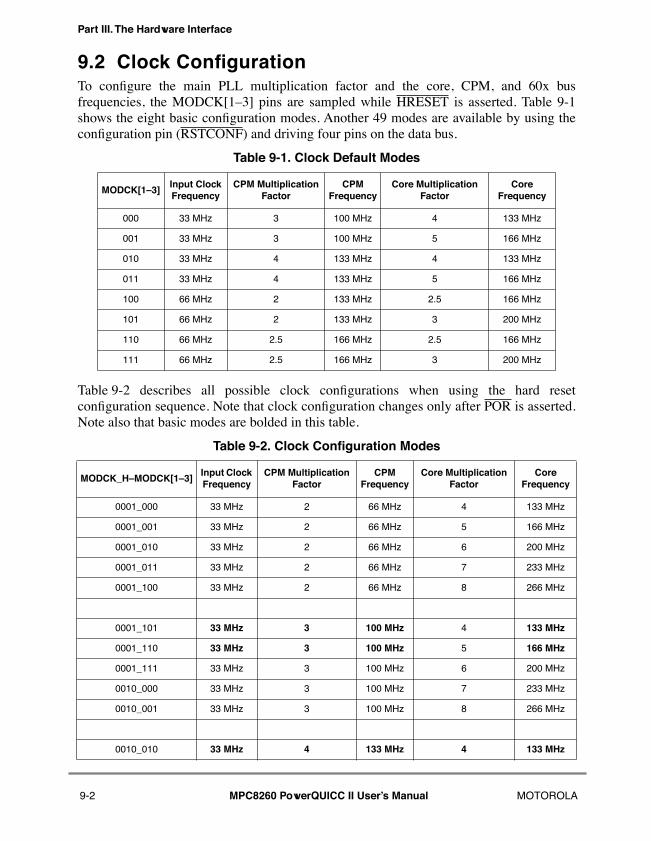
Part III. The Hardware Interface
9.2 Clock ConÞgurationTo conÞgure the main PLL multiplication factor and the core, CPM, and 60x busfrequencies, the MODCK[1Ð3] pins are sampled while HRESET is asserted. Table 9-1shows the eight basic conÞguration modes. Another 49 modes are available by using theconÞguration pin (RSTCONF) and driving four pins on the data bus.
Table 9-2 describes all possible clock conÞgurations when using the hard resetconÞguration sequence. Note that clock conÞguration changes only after POR is asserted.Note also that basic modes are bolded in this table.
Table 9-1. Clock Default Modes
MODCK[1Ð3]Input Clock Frequency
CPM Multiplication Factor
CPM Frequency
Core Multiplication Factor
Core Frequency
000 33 MHz 3 100 MHz 4 133 MHz
001 33 MHz 3 100 MHz 5 166 MHz
010 33 MHz 4 133 MHz 4 133 MHz
011 33 MHz 4 133 MHz 5 166 MHz
100 66 MHz 2 133 MHz 2.5 166 MHz
101 66 MHz 2 133 MHz 3 200 MHz
110 66 MHz 2.5 166 MHz 2.5 166 MHz
111 66 MHz 2.5 166 MHz 3 200 MHz
Table 9-2. Clock Configuration Modes
MODCK_HÐMODCK[1Ð3]Input Clock Frequency
CPM Multiplication Factor
CPMFrequency
Core Multiplication Factor
CoreFrequency
0001_000 33 MHz 2 66 MHz 4 133 MHz
0001_001 33 MHz 2 66 MHz 5 166 MHz
0001_010 33 MHz 2 66 MHz 6 200 MHz
0001_011 33 MHz 2 66 MHz 7 233 MHz
0001_100 33 MHz 2 66 MHz 8 266 MHz
0001_101 33 MHz 3 100 MHz 4 133 MHz
0001_110 33 MHz 3 100 MHz 5 166 MHz
0001_111 33 MHz 3 100 MHz 6 200 MHz
0010_000 33 MHz 3 100 MHz 7 233 MHz
0010_001 33 MHz 3 100 MHz 8 266 MHz
0010_010 33 MHz 4 133 MHz 4 133 MHz
9-2 MPC8260 PowerQUICC II UserÕs Manual MOTOROLA
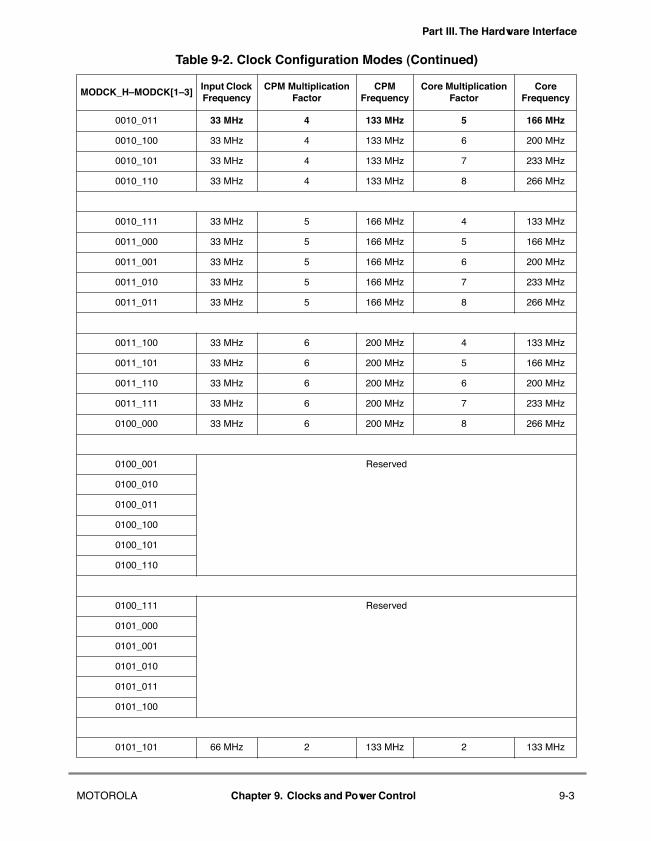
Part III. The Hardware Interface
0010_011 33 MHz 4 133 MHz 5 166 MHz
0010_100 33 MHz 4 133 MHz 6 200 MHz
0010_101 33 MHz 4 133 MHz 7 233 MHz
0010_110 33 MHz 4 133 MHz 8 266 MHz
0010_111 33 MHz 5 166 MHz 4 133 MHz
0011_000 33 MHz 5 166 MHz 5 166 MHz
0011_001 33 MHz 5 166 MHz 6 200 MHz
0011_010 33 MHz 5 166 MHz 7 233 MHz
0011_011 33 MHz 5 166 MHz 8 266 MHz
0011_100 33 MHz 6 200 MHz 4 133 MHz
0011_101 33 MHz 6 200 MHz 5 166 MHz
0011_110 33 MHz 6 200 MHz 6 200 MHz
0011_111 33 MHz 6 200 MHz 7 233 MHz
0100_000 33 MHz 6 200 MHz 8 266 MHz
0100_001 Reserved
0100_010
0100_011
0100_100
0100_101
0100_110
0100_111 Reserved
0101_000
0101_001
0101_010
0101_011
0101_100
0101_101 66 MHz 2 133 MHz 2 133 MHz
Table 9-2. Clock Configuration Modes (Continued)
MODCK_HÐMODCK[1Ð3]Input Clock Frequency
CPM Multiplication Factor
CPMFrequency
Core Multiplication Factor
CoreFrequency
MOTOROLA Chapter 9. Clocks and Power Control 9-3
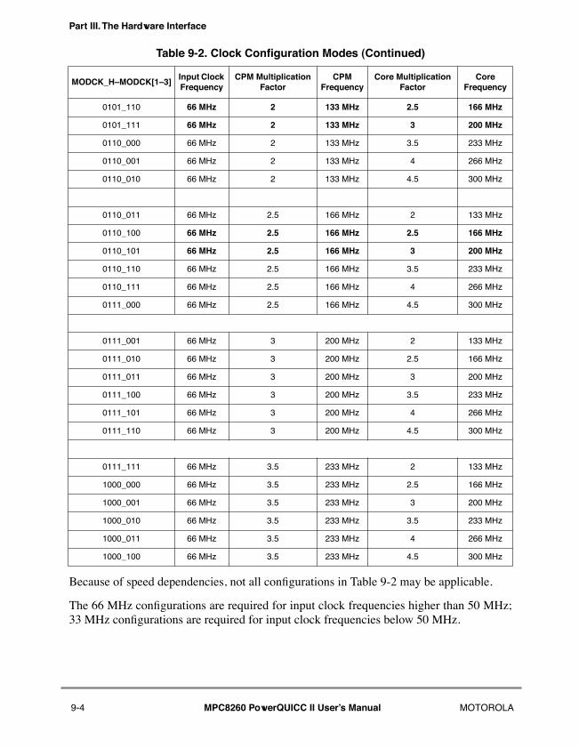
Part III. The Hardware Interface
Because of speed dependencies, not all conÞgurations in Table 9-2 may be applicable.
The 66 MHz conÞgurations are required for input clock frequencies higher than 50 MHz;33 MHz conÞgurations are required for input clock frequencies below 50 MHz.
0101_110 66 MHz 2 133 MHz 2.5 166 MHz
0101_111 66 MHz 2 133 MHz 3 200 MHz
0110_000 66 MHz 2 133 MHz 3.5 233 MHz
0110_001 66 MHz 2 133 MHz 4 266 MHz
0110_010 66 MHz 2 133 MHz 4.5 300 MHz
0110_011 66 MHz 2.5 166 MHz 2 133 MHz
0110_100 66 MHz 2.5 166 MHz 2.5 166 MHz
0110_101 66 MHz 2.5 166 MHz 3 200 MHz
0110_110 66 MHz 2.5 166 MHz 3.5 233 MHz
0110_111 66 MHz 2.5 166 MHz 4 266 MHz
0111_000 66 MHz 2.5 166 MHz 4.5 300 MHz
0111_001 66 MHz 3 200 MHz 2 133 MHz
0111_010 66 MHz 3 200 MHz 2.5 166 MHz
0111_011 66 MHz 3 200 MHz 3 200 MHz
0111_100 66 MHz 3 200 MHz 3.5 233 MHz
0111_101 66 MHz 3 200 MHz 4 266 MHz
0111_110 66 MHz 3 200 MHz 4.5 300 MHz
0111_111 66 MHz 3.5 233 MHz 2 133 MHz
1000_000 66 MHz 3.5 233 MHz 2.5 166 MHz
1000_001 66 MHz 3.5 233 MHz 3 200 MHz
1000_010 66 MHz 3.5 233 MHz 3.5 233 MHz
1000_011 66 MHz 3.5 233 MHz 4 266 MHz
1000_100 66 MHz 3.5 233 MHz 4.5 300 MHz
Table 9-2. Clock Configuration Modes (Continued)
MODCK_HÐMODCK[1Ð3]Input Clock Frequency
CPM Multiplication Factor
CPMFrequency
Core Multiplication Factor
CoreFrequency
9-4 MPC8260 PowerQUICC II UserÕs Manual MOTOROLA
Part III. The Hardware Interface
9.3 External Clock InputsThe input clock source to the PLL is an external clock oscillator at the bus frequency. ThePLL skew elimination between the CLOCKIN pin and the internal bus clock is guaranteed.
9.4 Main PLLThe main PLL performs frequency multiplication and skew elimination. It allows theprocessor to operate at a high internal clock frequency using a low-frequency clock input,which has two immediate beneÞts: A lower clock input frequency reduces overallelectromagnetic interference generated by the system, and oscillating at differentfrequencies eliminates the need for another oscillator to the system.
9.4.1 PLL Block DiagramFigure 9-1 shows how clocking is implemented and the interdependencies of the SCMRÞelds:
¥ BUSDFÑ60x bus division factor
¥ CPMDFÑCPM division factor. This value is always 1.
¥ PLLDFÑPLL pre-divider value. Ensures that PLLMF is an integer value regardless of whether CPM_CLK/CLKIN is an integer.
¥ PLLMFÑPLL multiplication factor
These Þelds are described in detail in Table 9-5.
Figure 9-1. System PLL Block Diagram
The reference signal (CLKIN) goes to the phase comparator that controls the direction (upor down) that the charge pump drives the voltage across the external Þlter capacitor (XFC).
÷ (PLLDF + 1)
VCO_OUT
´ 2(PLLMF + 1)÷ (CPMDF + 1)
÷ (BUSDF + 1)
÷ 4
22 (DFBRG + 1)
CPM_CLKCPM_CLK_90°
BUS_CLK (= CLKIN)BUS_CLK_90°
SCC_CLKSCC_CLK_90°
BRG
CLKIN
(÷2)
PLLDF ensures that PLLMF is an integer, according to thefollowing formula:
PLLMF =CPM_CLK
CLKIN ´ (PLLDF + 1) Ð 1
General-Purpose Divider
(2*CPM_CLK)
MOTOROLA Chapter 9. Clocks and Power Control 9-5
Part III. The Hardware Interface
The direction selected depends on whether the feedback signal phase lags or leads thereference signal. The output of the charge pump drives the VCO whose output frequency isdivided and fed back to the phase comparator for comparison with the reference signal,CLKIN. Ranging between 1 and 4,096, the PLL multiplication factor is held in the systemclock mode register (SCMR[PLLMF]). Also, when the PLL is operating, its outputfrequency is twice the CPM frequency. This double frequency is required to generate theCPM_CLK and CPM_CLK_90 clocks. See the block diagram in Figure 9-1 for details.
On initial system power-up, power-on reset (PORESET) should be asserted by externallogic for 16 input clocks after a valid level is reached on the power supply. Wheneverpower-on reset is asserted, SCMR[PLLMF, PLLDF] are programmed by the conÞgurationpins; see Table 9-2. This value then drives the clock block to generate the correct CPM andbus frequencies.
9.4.2 Skew EliminationThe PLL can tighten synchronous timings by eliminating skew between phases of theinternal clock and the external clock entering the chip (CLOCKIN). Skew elimination isalways active when the PLL is enabled. Disabling the PLL can greatly increase clock skew.
9.5 Clock DividersThe PLL output is twice the maximum frequency needed for all the clocks. The PLL outputis sent to general-purpose dividers (CPMDF, BUSDF), either of which can divide thedouble clock by a programmable number between 1 and 16. The delay is the same for alldividers independent on the programmable number, so the clocks are synchronized.
The output of each divider has two phases, one shifted 90¡ from the other, as shown inTable 9-1. Each phase has a 50% duty cycle.
9.6 The MPC8260Õs Internal Clock SignalsThe internal logic of the MPC8260 uses the following internal clock lines:
¥ CPM general system clocks (CPM_CLK, CPM_CLK_90)
¥ 60x bus, core bus (BUS_CLK, BUS_CLK_90)
¥ SCC clocks (SCC_CLK, SCC_CLK_90)
¥ Baud-rate generator clock (BRG_CLK)
The PLL synchronizes these clock signals to each other (but does not synchronize toBRG_CLK).
9-6 MPC8260 PowerQUICC II UserÕs Manual MOTOROLA
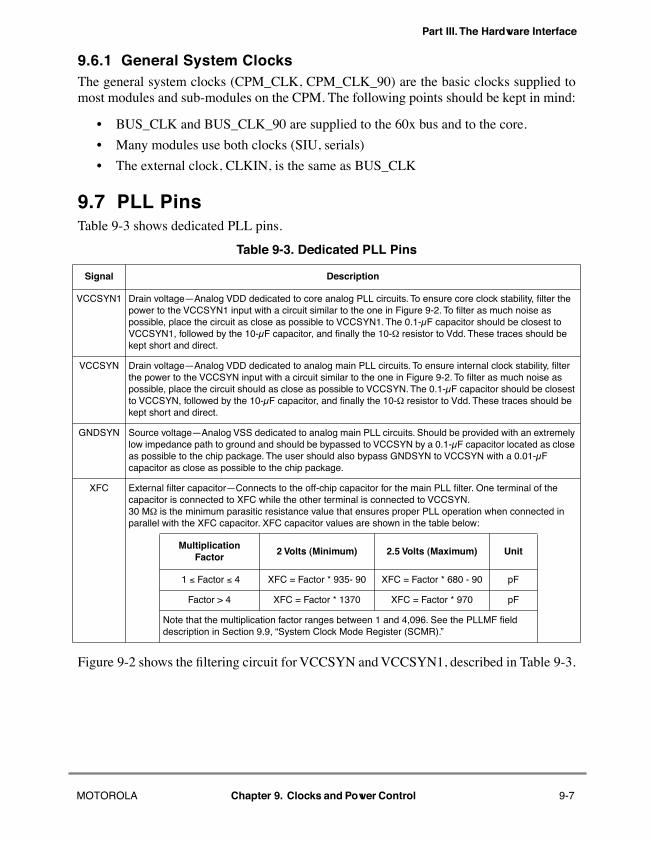
Part III. The Hardware Interface
9.6.1 General System ClocksThe general system clocks (CPM_CLK, CPM_CLK_90) are the basic clocks supplied tomost modules and sub-modules on the CPM. The following points should be kept in mind:
¥ BUS_CLK and BUS_CLK_90 are supplied to the 60x bus and to the core.
¥ Many modules use both clocks (SIU, serials)
¥ The external clock, CLKIN, is the same as BUS_CLK
9.7 PLL Pins Table 9-3 shows dedicated PLL pins.
Figure 9-2 shows the Þltering circuit for VCCSYN and VCCSYN1, described in Table 9-3.
Table 9-3. Dedicated PLL Pins
Signal Description
VCCSYN1 Drain voltageÑAnalog VDD dedicated to core analog PLL circuits. To ensure core clock stability, Þlter the power to the VCCSYN1 input with a circuit similar to the one in Figure 9-2. To Þlter as much noise as possible, place the circuit as close as possible to VCCSYN1. The 0.1-µF capacitor should be closest to VCCSYN1, followed by the 10-µF capacitor, and Þnally the 10-W resistor to Vdd. These traces should be kept short and direct.
VCCSYN Drain voltageÑAnalog VDD dedicated to analog main PLL circuits. To ensure internal clock stability, Þlter the power to the VCCSYN input with a circuit similar to the one in Figure 9-2. To Þlter as much noise as possible, place the circuit should as close as possible to VCCSYN. The 0.1-µF capacitor should be closest to VCCSYN, followed by the 10-µF capacitor, and Þnally the 10-W resistor to Vdd. These traces should be kept short and direct.
GNDSYN Source voltageÑAnalog VSS dedicated to analog main PLL circuits. Should be provided with an extremely low impedance path to ground and should be bypassed to VCCSYN by a 0.1-µF capacitor located as close as possible to the chip package. The user should also bypass GNDSYN to VCCSYN with a 0.01-µF capacitor as close as possible to the chip package.
XFC External Þlter capacitorÑConnects to the off-chip capacitor for the main PLL Þlter. One terminal of the capacitor is connected to XFC while the other terminal is connected to VCCSYN. 30 MW is the minimum parasitic resistance value that ensures proper PLL operation when connected in parallel with the XFC capacitor. XFC capacitor values are shown in the table below:
Multiplication Factor
2 Volts (Minimum) 2.5 Volts (Maximum) Unit
1 £ Factor £ 4 XFC = Factor * 935- 90 XFC = Factor * 680 - 90 pF
Factor > 4 XFC = Factor * 1370 XFC = Factor * 970 pF
Note that the multiplication factor ranges between 1 and 4,096. See the PLLMF Þeld description in Section 9.9, ÒSystem Clock Mode Register (SCMR).Ó
MOTOROLA Chapter 9. Clocks and Power Control 9-7
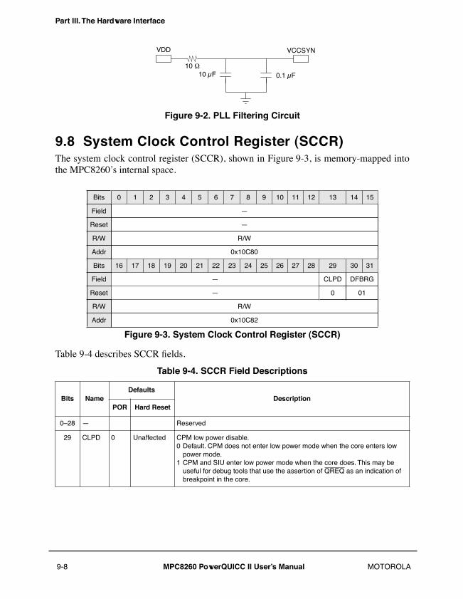
Part III. The Hardware Interface
Figure 9-2. PLL Filtering Circuit
9.8 System Clock Control Register (SCCR)The system clock control register (SCCR), shown in Figure 9-3, is memory-mapped intothe MPC8260Õs internal space.
Table 9-4 describes SCCR Þelds.
Bits 0 1 2 3 4 5 6 7 8 9 10 11 12 13 14 15
Field Ñ
Reset Ñ
R/W R/W
Addr 0x10C80
Bits 16 17 18 19 20 21 22 23 24 25 26 27 28 29 30 31
Field Ñ CLPD DFBRG
Reset Ñ 0 01
R/W R/W
Addr 0x10C82
Figure 9-3. System Clock Control Register (SCCR)
Table 9-4. SCCR Field Descriptions
Bits NameDefaults
DescriptionPOR Hard Reset
0Ð28 Ñ Reserved
29 CLPD 0 Unaffected CPM low power disable. 0 Default. CPM does not enter low power mode when the core enters low
power mode.1 CPM and SIU enter low power mode when the core does. This may be
useful for debug tools that use the assertion of QREQ as an indication of breakpoint in the core.
10 W
VDD
0.1 µF10 µF
VCCSYN
9-8 MPC8260 PowerQUICC II UserÕs Manual MOTOROLA
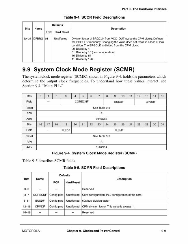
Part III. The Hardware Interface
9.9 System Clock Mode Register (SCMR)The system clock mode register (SCMR), shown in Figure 9-4, holds the parameters whichdetermine the output clock frequencies. To understand how these values interact, seeSection 9.4, ÒMain PLL.Ó
Table 9-5 describes SCMR Þelds.
30Ð31 DFBRG 01 Unaffected Division factor of BRGCLK from VCO_OUT (twice the CPM clock). DeÞnes the BRGCLK frequency. Changing the value does not result in a loss of lock condition. The BRGCLK is divided from the CPM clock.00 Divide by 401 Divide by 16 (normal operation)10 Divide by 6411 Divide by 128
Bits 0 1 2 3 4 5 6 7 8 9 10 11 12 13 14 15
Field Ñ CORECNF BUSDF CPMDF
Reset See Table 9-5
R/W R
Addr 0x10C88
Bits 16 17 18 19 20 21 22 23 24 25 26 27 28 29 30 31
Field Ñ PLLDF PLLMF
Reset See Table 9-5
R/W R
Addr 0x10C8A
Figure 9-4. System Clock Mode Register (SCMR)
Table 9-5. SCMR Field Descriptions
Bits NameDefaults
DescriptionPOR Hard Reset
0Ð2 Ñ Ñ Ñ Reserved
3Ð7 CORECNF ConÞg pins Unaffected Core conÞguration. PLL conÞguration of the core.
8Ð11 BUSDF ConÞg pins Unaffected 60x bus division factor
12Ð15 CPMDF ConÞg pins Unaffected CPM division factor. This value is always 1.
16Ð18 Ñ Ñ Ñ Reserved
Table 9-4. SCCR Field Descriptions
Bits NameDefaults
DescriptionPOR Hard Reset
MOTOROLA Chapter 9. Clocks and Power Control 9-9
Part III. The Hardware Interface
The relationships among these parameters are described in the formulas in Figure 9-5.
Figure 9-5. Relationships of SCMR Parameters
9.10 Basic Power StructureThe I/O buffers, logic, and clock block are fed by a 3.3-V power supply that allows them tofunction in a TTL-compatible voltage range. Internal logic can be fed by a 2.0-V sourceconsiderably reducing power consumption. The PLL is fed by a separate power supply(VCCSYN) to achieve a highly stable output frequency. The VCCSYN value is equal to theinternal supply (2.0 V).
The MPC8260 supports the two following power modes:
¥ Full mode: Both the chip PLL and core PLL work.
¥ Stop mode: Main PLL is working, core PLL is stopped, internal clocks are disabled.
Ñ When stop mode is entered, software sets the sleep bit in the core (HID0[10] = 1) and the clock block freezes all clocks to the chip (the core clock and all other clocks) the main PLL remains active
Ñ When stop mode is exited, the SRESET_B input must be asserted to the chip, the clock block resumes clocks to all blocks and then releases the reset to the whole chip.
19 PLLDF ConÞg pins Unaffected PLL pre-divider value. Ensures that PLLMF is an integer value regardless of whether CPM_CLK/CLKIN is an integer.0 The ratio, CPM_CLK/CLKIN, is an integer1 The ratio, CPM_CLK/CLKIN, is not an integerPLL division factor can be either 1 or 2.
20Ð31 PLLMF ConÞg pins Unaffected PLL multiplication factor. (A PLLMF value of 0x000 corresponds to 1, and 0xFFF to 4,096.) The VCO output is divided to generate the feedback signal that goes to the phase comparator. PLLMF and PLLDF bits control the value of the divider in the PLL feedback loop. The phase comparator determines the phase shift between the feedback signal and the reference clock. This difference causes an increase or decrease in the VCO output frequency.
Table 9-5. SCMR Field Descriptions (Continued)
Bits NameDefaults
DescriptionPOR Hard Reset
PLLMF = CPM_CLKCLKIN
´ (PLLDF + 1) Ð 1
BUSDF = (PLLMF + 1) ´ 2(PLLDF + 1)
Ð 1
9-10 MPC8260 PowerQUICC II UserÕs Manual MOTOROLA
Chapter 10 Memory Controller100100
The memory controller is responsible for controlling a maximum of twelve memory banksshared by a high performance SDRAM machine, a general-purpose chip-select machine(GPCM), and three user-programmable machines (UPMs). It supports a glueless interfaceto synchronous DRAM (SDRAM), SRAM, EPROM, ßash EPROM, burstable RAM,regular DRAM devices, extended data output DRAM devices, and other peripherals. Thisßexible memory controller allows the implementation of memory systems with veryspeciÞc timing requirements.
¥ The SDRAM machine provides an interface to synchronous DRAMs, using SDRAM pipelining, bank interleaving, and back-to-back page mode to achieve the highest performance.
¥ The GPCM provides interfacing for simpler, lower-performance memory resources and memory-mapped devices. The GPCM has inherently lower performance because it does not support bursting. For this reason, GPCM-controlled banks are used primarily for boot-loading and access to low-performance memory-mapped peripherals.
¥ The UPM supports address multiplexing of the external bus, refresh timers, and generation of programmable control signals for row address and column address strobes to allow for a glueless interface to DRAMs, burstable SRAMs, and almost any other kind of peripheral. The refresh timers allow refresh cycles to be initiated. The UPM can be used to generate different timing patterns for the control signals that govern a memory device. These patterns deÞne how the external control signals behave during a read, write, burst-read, or burst- write access request. Refresh timers are also available to periodically generate user-deÞned refresh cycles.
Unless stated otherwise, this chapter describes the 60x bus memory controller. The localbus memory controller provides the same functionality as the 60x bus memory controllerexcept 64-bit port size ECC and external master support.
MOTOROLA Chapter 10. Memory Controller 10-1
Part III. The Hardware Interface
The MPC8260 supports the following new features as compared to the MPC860 andMPC850.
¥ The synchronous DRAM machine enables back-to-back memory read or write operations using page mode, pipelined operation and bank interleaving for high-performance systems.
¥ The memory controller supports the local bus and the 60x bus in parallel. The 60x bus and the local bus share twelve memory banks as well as two SDRAM machines, three user-programmable machines (UPMs) and GPCMs.
¥ The memory controller supports atomic operation.
¥ The memory controller supports read-modify-write (RMW) data parity check.
¥ The memory controller supports ECC data check and correction.
¥ Two data buffer controls (one for the local bus).
¥ ECC/parity byte select pin, which enables a fast, glueless connection to ECC/RMW-parity devices.
¥ 18-bit address and 32-bit local data bus memory controller. The local bus memory controller supports the following:
Ñ 8-, 16-, and 32-bit port sizes
Ñ Parity checking and generation
Ñ Ability to work in parallel with the 60x bus memory controller
Unless stated otherwise, this chapter describes the 60x bus memory controller. The local bus memory controller provides the same functionality as the 60x bus memory controller except 64-bit port size, ECC, and external master support.
¥ Flexible chip-select assignmentÑThe 60x bus and local bus share twelve chip-select lines (controlled by a memory controller bank). The user can allocate the twelve banks as needed between the 60x bus and the local bus.
¥ Flexible UPM assignmentÑThe user can assign any of the three UPMs to the 60x bus or the Local bus
Figure 10-1 shows the dual-bus architecture.
10-2 MPC8260 PowerQUICC II UserÕs Manual MOTOROLA
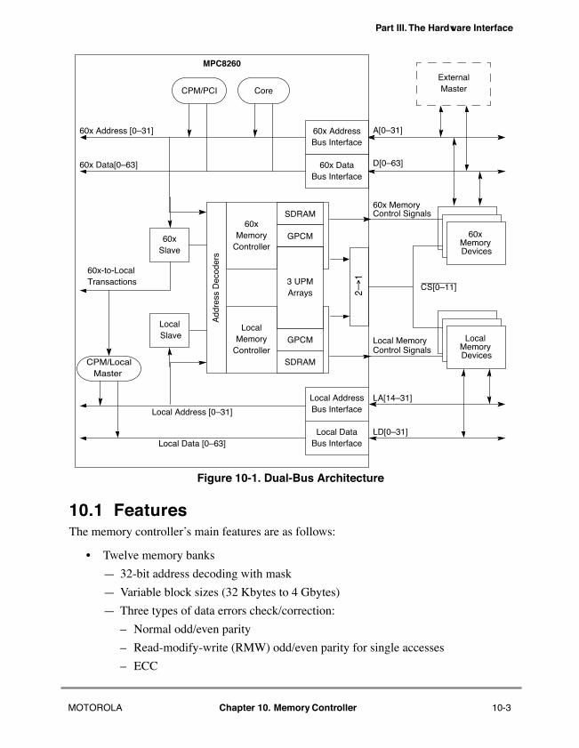
Part III. The Hardware Interface
Figure 10-1. Dual-Bus Architecture
10.1 FeaturesThe memory controllerÕs main features are as follows:
¥ Twelve memory banks
Ñ 32-bit address decoding with mask
Ñ Variable block sizes (32 Kbytes to 4 Gbytes)
Ñ Three types of data errors check/correction:
Ð Normal odd/even parity
Ð Read-modify-write (RMW) odd/even parity for single accesses
Ð ECC
MPC8260
A[0Ð31]
D[0Ð63]
LA[14Ð31]
LD[0Ð31]
ExternalMaster
60x
Local
60x MemoryControl Signals
CS[0Ð11]
Local MemoryControl Signals
60x AddressBus Interface
Local AddressBus Interface
Local DataBus Interface
60x Address [0Ð31]
Local Address [0Ð31]
60x Data[0Ð63]
Local Data [0Ð63]
GPCM
SDRAM
LocalMemory
Controller
SDRAM
GPCM60x
MemoryController
3 UPMArrays
Add
ress
Dec
oder
s
Local
60x-to-Local
Core
CPM/Local2®
1
60x
Transactions
60x DataBus Interface
CPM/PCI
Master
Slave
SlaveMemory Devices
Memory Devices
MOTOROLA Chapter 10. Memory Controller 10-3
Part III. The Hardware Interface
Ñ Write-protection capability
Ñ Control signal generation machine selection on a per-bank basis
Ñ Flexible chip-select assignment between the 60x bus and the local bus
Ñ Supports internal or external masters on the 60x bus
Ñ Data buffer controls activated on a per-bank basis
Ñ Atomic operation
Ñ Extensive external memory-controller/bus-slave support
Ñ ECC/parity byte-select
Ñ Data pipeline to reduce data setup time for synchronous devices
¥ Synchronous DRAM machine (60x or local bus)
Ñ Provides the control functions and signals for glueless connection to JEDEC-compliant SDRAM devices
Ñ Back-to-back page mode for consecutive, back-to-back accesses
Ñ Supports 2-, 4- and 8-way bank interleaving
Ñ Supports SDRAM port size of 64-bit (60x only), 32-bit, 16-bit and 8-bit
Ñ Supports external address and/or command lines buffering
¥ General-purpose chip-select machine (GPCM)Ñ60x or local bus
Ñ Compatible with SRAM, EPROM, FEPROM, and peripherals
Ñ Global (boot) chip-select available at system reset
Ñ Boot chip-select support for 8-, 16-, 32-, and 64-bit devices
Ñ Minimum two clock accesses to external device
Ñ Eight byte write enable signals (WE)Ñfour on the local bus
Ñ Output enable signal (OE)
Ñ External access termination signal (GTA)
¥ Three UPMs
Ñ Each machine can be assigned to the 60x or local bus.
Ñ Programmable-array-based machine controls external signal timing with a granularity of up to one quarter of an external bus clock period
Ñ User-speciÞed control-signal patterns run when an internal or external master requests a single-beat or burst read or write access.
Ñ UPM refresh timer runs a user-speciÞed control signal pattern to support refresh
Ñ User-speciÞed control-signal patterns can be initiated by software
10-4 MPC8260 PowerQUICC II UserÕs Manual MOTOROLA
Part III. The Hardware Interface
Ñ Each UPM can be deÞned to support DRAM devices with depths of 64, 128, 256, and 512 Kbytes, and 1, 2, 4, 8, 16, 32, 64, 128, and 256 Mbytes
Ð Chip-select line
Ð Byte-select lines
Ð Six external general-purpose lines
Ñ Supports 8-, 16-, 32-, and 64-bit memory port sizes, 8-, 16-, and 32-bit port sizes on the local bus
Ñ Page mode support for successive transfers within a burst
Ñ Internal address multiplexing for all on-chip bus masters supporting 64-, 128-, 256-, and 512-Kbyte, and 1-, 2-, 4-, 8-, 16-, 32-, 64-, 128-, 256-Mbyte page banks
10.2 Basic ArchitectureThe memory controller consists of three basic machines:
¥ Synchronous DRAM machine
¥ General-purpose chip-select machine (GPCM)
¥ Three UPMs
Each bank can be assigned to any one of these machines via BRx[MS] as shown inFigure 10-2. The MS and MxMR[BS] bits (for UPMs) assign banks to the 60x bus or localbus, as shown in Figure 10-2. Addresses are decoded by comparing (A[0Ð16] bit-wise andORx[AM]) with BRx[BA]. If an address match occurs in multiple banks, the lowestnumbered bank has priority. However, if a 60x bus access hits a bank allocated to the localbus, the access is transferred to the local bus. Local bus access hits to 60x assigned banksare ignored.
When a memory address matches BRx[BA], the corresponding machine takes ownershipof the external signals that control access and maintains control until the cycle ends.
MOTOROLA Chapter 10. Memory Controller 10-5
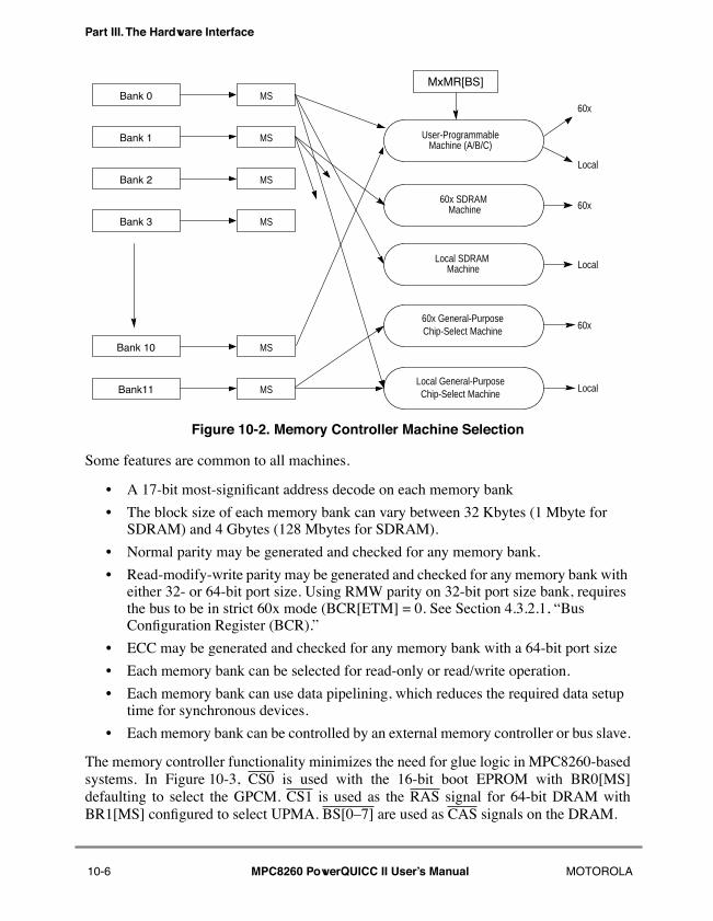
Part III. The Hardware Interface
Figure 10-2. Memory Controller Machine Selection
Some features are common to all machines.
¥ A 17-bit most-signiÞcant address decode on each memory bank
¥ The block size of each memory bank can vary between 32 Kbytes (1 Mbyte for SDRAM) and 4 Gbytes (128 Mbytes for SDRAM).
¥ Normal parity may be generated and checked for any memory bank.
¥ Read-modify-write parity may be generated and checked for any memory bank with either 32- or 64-bit port size. Using RMW parity on 32-bit port size bank, requires the bus to be in strict 60x mode (BCR[ETM] = 0. See Section 4.3.2.1, ÒBus ConÞguration Register (BCR).Ó
¥ ECC may be generated and checked for any memory bank with a 64-bit port size
¥ Each memory bank can be selected for read-only or read/write operation.
¥ Each memory bank can use data pipelining, which reduces the required data setup time for synchronous devices.
¥ Each memory bank can be controlled by an external memory controller or bus slave.
The memory controller functionality minimizes the need for glue logic in MPC8260-basedsystems. In Figure 10-3, CS0 is used with the 16-bit boot EPROM with BR0[MS]defaulting to select the GPCM. CS1 is used as the RAS signal for 64-bit DRAM withBR1[MS] conÞgured to select UPMA. BS[0Ð7] are used as CAS signals on the DRAM.
User-Programmable
Local General-Purpose
Bank 0
Bank 1
Bank 2
Bank 3
Bank 10
Bank11
MS
MS
MS
MS
MS
MS Chip-Select Machine
Local SDRAM Local
60x
Local
MxMR[BS]
60x SDRAM 60x
Local
60x General-PurposeChip-Select Machine 60x
Machine (A/B/C)
Machine
Machine
10-6 MPC8260 PowerQUICC II UserÕs Manual MOTOROLA
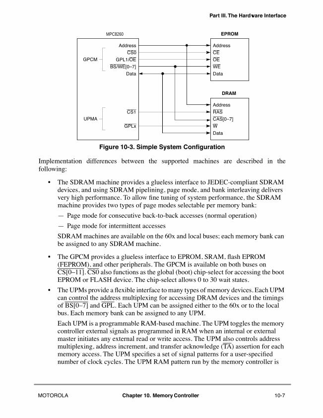
Part III. The Hardware Interface
Figure 10-3. Simple System Configuration
Implementation differences between the supported machines are described in thefollowing:
¥ The SDRAM machine provides a glueless interface to JEDEC-compliant SDRAM devices, and using SDRAM pipelining, page mode, and bank interleaving delivers very high performance. To allow Þne tuning of system performance, the SDRAM machine provides two types of page modes selectable per memory bank:
Ñ Page mode for consecutive back-to-back accesses (normal operation)
Ñ Page mode for intermittent accesses
SDRAM machines are available on the 60x and local buses; each memory bank can be assigned to any SDRAM machine.
¥ The GPCM provides a glueless interface to EPROM, SRAM, ßash EPROM (FEPROM), and other peripherals. The GPCM is available on both buses on CS[0Ð11]. CS0 also functions as the global (boot) chip-select for accessing the boot EPROM or FLASH device. The chip-select allows 0 to 30 wait states.
¥ The UPMs provide a ßexible interface to many types of memory devices. Each UPM can control the address multiplexing for accessing DRAM devices and the timings of BS[0Ð7] and GPL. Each UPM can be assigned either to the 60x or to the local bus. Each memory bank can be assigned to any UPM.
Each UPM is a programmable RAM-based machine. The UPM toggles the memory controller external signals as programmed in RAM when an internal or external master initiates any external read or write access. The UPM also controls address multiplexing, address increment, and transfer acknowledge (TA) assertion for each memory access. The UPM speciÞes a set of signal patterns for a user-speciÞed number of clock cycles. The UPM RAM pattern run by the memory controller is
Address
CE
OE
WE
Data
EPROM
RAS
CAS[0Ð7]
W
Data
DRAM
CS1
GPLx
Data
BS/WE[0Ð7]
GPL1/OE
CS0
Address
Address
UPMA
GPCM
MPC8260
MOTOROLA Chapter 10. Memory Controller 10-7
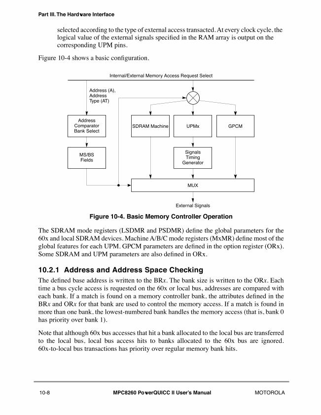
Part III. The Hardware Interface
selected according to the type of external access transacted. At every clock cycle, the logical value of the external signals speciÞed in the RAM array is output on the corresponding UPM pins.
Figure 10-4 shows a basic conÞguration.
Figure 10-4. Basic Memory Controller Operation
The SDRAM mode registers (LSDMR and PSDMR) deÞne the global parameters for the60x and local SDRAM devices. Machine A/B/C mode registers (MxMR) deÞne most of theglobal features for each UPM. GPCM parameters are deÞned in the option register (ORx).Some SDRAM and UPM parameters are also deÞned in ORx.
10.2.1 Address and Address Space CheckingThe deÞned base address is written to the BRx. The bank size is written to the ORx. Eachtime a bus cycle access is requested on the 60x or local bus, addresses are compared witheach bank. If a match is found on a memory controller bank, the attributes deÞned in theBRx and ORx for that bank are used to control the memory access. If a match is found inmore than one bank, the lowest-numbered bank handles the memory access (that is, bank 0has priority over bank 1).
Note that although 60x bus accesses that hit a bank allocated to the local bus are transferredto the local bus, local bus access hits to banks allocated to the 60x bus are ignored.60x-to-local bus transactions has priority over regular memory bank hits.
AddressComparatorBank Select
UPMx GPCM
MS/BSFields
SignalsTiming
Generator
MUX
Internal/External Memory Access Request Select
Address (A),AddressType (AT)
External Signals
SDRAM Machine
10-8 MPC8260 PowerQUICC II UserÕs Manual MOTOROLA
Part III. The Hardware Interface
10.2.2 Page Hit CheckingThe SDRAM machine supports page-mode operation. Each time a page is activated on theSDRAM device, the SDRAM machine stores its address in a page register. The pageinformation, which the user writes to the ORx register, is used along with the bank size tocompare page bits of the address to the page register each time a bus-cycle access isrequested. If a match is found together with bank match, the bus cycle is deÞned as a pagehit. An open page is automatically closed by the SDRAM machine if the bus becomes idle,unless ORx[PMSEL] is set.
10.2.3 Error Checking and Correction (ECC)ECC can be conÞgured for any bank as long as it is assigned to the 60x bus and is connectedto a 64-bit port size memory. ECC is generated and checked on a 64-bit basis using DP[0Ð7]for the bank if BRx[DECC] = 11. If ECC is used, single errors can be corrected and alldouble-bit errors can be detected.
10.2.4 Parity Generation and CheckingParity can be conÞgured for any bank, if it is preferred. Parity is generated and checked ona per-byte basis using DP[0Ð7] or LDP[0Ð3] for the bank if BR[DECC] = 01 for normalparity and 10 for RMW parity. SIUMCR[EPAR] determines the global type of parity (oddor even).
Note that RMW parity can be used only for 32- or 64-bit port size banks. Also, using RMWparity on a 32-bit port size bank, requires that the bus is placed is strict 60x mode. This isdone by setting BCR[ETM] (BCR[LETM] for the local bus) see Section 4.3.2.1, ÒBusConÞguration Register (BCR),Ó for more details.
10.2.5 Transfer Error Acknowledge (TEA) GenerationThe memory controller asserts the transfer error acknowledge signal (TEA) (if enabled) inthe following cases:
¥ An unaligned or burst access is attempted to internal MPC8260 space (registers or dual-port RAM).
¥ The core or an external master attempts a burst access to the local bus address space
¥ A bus monitor timeout
10.2.6 Machine Check Interrupt (MCP) GenerationThe memory controller asserts machine check interrupt (MCP) in the following cases:
¥ A parity error
¥ An ECC double-bit error
¥ An ECC single bit error when the maximum number of ECC errors has been reached
MOTOROLA Chapter 10. Memory Controller 10-9
Part III. The Hardware Interface
10.2.7 Data Buffer Controls (BCTLx)The memory controller provides two data buffer controls for the 60x bus (BCTL0 andBCTL1) and one for the local bus (LWR). These controls are activated when a GPCM- orUPM-controlled bank is accessed. The BCTLx controls can be disabled by settingORx[BCTLD]. Access to SDRAM-machine controlled bank does not activate the BCTLxcontrols. The BCTL signals are asserted on the rising edge of CLKIN on the Þrst cycle ofthe memory controller operation. They are negated on the rising edge of CLKIN after thelast assertion of PSDVAL of the access is asserted. (See Section 10.2.13, ÒPartial Data ValidIndication (PSDVAL).Ó) If back-to-back memory controller operations are pending,BCTLx is not negated.
The BCTL signals have a programmable polarity. See Section 4.3.2.6, ÒSIU ModuleConÞguration Register (SIUMCR).Ó
10.2.8 Atomic Bus Operation The MPC8260 supports the following kinds of atomic bus operations BRx[ATOM]:
¥ Read-after-write (RAWA). When a write access hits a memory bank in which ATOM = 01, the MPC8260 locks the bus for the exclusive use of the accessing master (internal or external).
While the bus is locked, no other device can be granted the bus. The lock is released when the master that created the lock access the same bank with a read transaction. If the master fails to release the lock within 256 bus clock cycles, the lock is released and a special interrupt is generated. This feature is intended for CAM operations.
¥ Write-after-read (WARA). When a read access hit a memory bank in which ATOM = 10, the MPC8260 locks the bus for the exclusive use of the accessing master (internal or external).
During the lock period, no other device can be granted bus mastership. The lock is released when the device that created the lock access the same bank with a write transaction. If the device fails to release the lock within 256 bus clock cycles, the lock is released and a special interrupt is generated.
Note that this mechanism does not replace the PowerPC reservation mechanism.
10.2.9 Data Pipelining Multiple-MPC8260 systems that use that use data checking, such as ECC or parity, face atiming problem when synchronous memories, such as SDRAM, are used. Because thesedevices can output data every cycle and because the data checking requires additional datasetup time, the timing constraints are extremely hard to meet. In such systems, the usershould set the data pipelining bit, BRx[DR]. This creates data pipelining of one stage withinthe memory controller in which the data check calculations are done, thus eliminating theadditional data setup time requirement.
10-10 MPC8260 PowerQUICC II UserÕs Manual MOTOROLA
Part III. The Hardware Interface
Note that this feature cannot be used with L2 cacheable banks and that in systems thatinvolve both PowerQUICC II-type masters and 60x compatible master, this feature can stillbe used on the 60x bus under the following restrictions:
1. The arbiter and the memory controller are in the same MPC8260.
2. The register Þeld BCR[NPQM] is setup correctly.
See ÒSection 10.9, ÒExternal Master Support (60x-Compatible Mode)Ó andÒSection 4.3.2.1, ÒBus ConÞguration Register (BCR).Ó
10.2.10 External Memory Controller Support The MPC8260 has an option to allocate speciÞc banks (address spaces) to be controlled byan external memory controller or bus slave, while retaining all the bank properties: portsize, data check/correction, atomic operation, and data pipelining. This is done byprogramming BRx and ORx[AM] and by setting the external memory controller bit,BRx[EMEMC]. This action automatically assigns the bank to the 60x bus. For an accessthat hits the bank, all bus acknowledgment signals (such as AACK, PSDVAL, and TA) andthe memory-device control strobes are driven by an external memory controller or slave. Ifthe device that initiates the transaction is internal to the MPC8260, the memory controllerhandles the port size, data checking, atomic locking, and data pipelining as if the accesswere governed by it.
This feature allows multiple MPC8260 systems to be connected in 60x-compatible modewithout loosing functionality and performance. It also make it easy to connect other60x-compatible slaves on the 60x bus.
10.2.11 External Address Latch Enable Signal (ALE)The memory controller provides control for an external address latch, needed on the 60xbus in 60x compatible mode. ALE is asserted for one clock cycle on the Þrst cycle of eachmemory-controller transaction. In this section, whenever ALE is not on a timing diagram,assume that it is asserted on the Þrst cycle in which CS can be asserted. Note that ALE isrelevant only on the 60x bus and only in 60x-compatible mode.
10.2.12 ECC/Parity Byte Select (PBSE)Systems that use ECC or read-modify-write parity, require an additional memory devicethat requires byte-select like a normal data device. ANDing BS[0Ð7] through external logicto achieve the logical function of this byte-select can affect the memory access timingbecause it adds a delay to the byte-select path. The MPC8260Õs memory controller providesoptional byte-select pins that are an internal AND of the eight byte selects, allowingglueless, faster connection to ECC/RMW-parity devices.
This option is enabled by setting SIUMCR[PBSE], as described in Section 4.3.2.6, ÒSIUModule ConÞguration Register (SIUMCR).Ó
MOTOROLA Chapter 10. Memory Controller 10-11
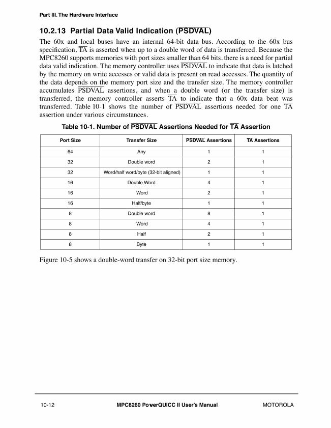
Part III. The Hardware Interface
10.2.13 Partial Data Valid Indication (PSDVAL)The 60x and local buses have an internal 64-bit data bus. According to the 60x busspeciÞcation, TA is asserted when up to a double word of data is transferred. Because theMPC8260 supports memories with port sizes smaller than 64 bits, there is a need for partialdata valid indication. The memory controller uses PSDVAL to indicate that data is latchedby the memory on write accesses or valid data is present on read accesses. The quantity ofthe data depends on the memory port size and the transfer size. The memory controlleraccumulates PSDVAL assertions, and when a double word (or the transfer size) istransferred, the memory controller asserts TA to indicate that a 60x data beat wastransferred. Table 10-1 shows the number of PSDVAL assertions needed for one TAassertion under various circumstances.
Figure 10-5 shows a double-word transfer on 32-bit port size memory.
Table 10-1. Number of PSDVAL Assertions Needed for TA Assertion
Port Size Transfer Size PSDVAL Assertions TA Assertions
64 Any 1 1
32 Double word 2 1
32 Word/half word/byte (32-bit aligned) 1 1
16 Double Word 4 1
16 Word 2 1
16 Half/byte 1 1
8 Double word 8 1
8 Word 4 1
8 Half 2 1
8 Byte 1 1
10-12 MPC8260 PowerQUICC II UserÕs Manual MOTOROLA
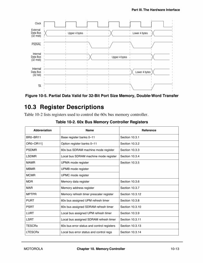
Part III. The Hardware Interface
Figure 10-5. Partial Data Valid for 32-Bit Port Size Memory, Double-Word Transfer
10.3 Register DescriptionsTable 10-2 lists registers used to control the 60x bus memory controller.
Table 10-2. 60x Bus Memory Controller Registers
Abbreviation Name Reference
BR0ÐBR11 Base register banks 0Ð11 Section 10.3.1
OR0ÐOR11] Option register banks 0Ð11 Section 10.3.2
PSDMR 60x bus SDRAM machine mode register Section 10.3.3
LSDMR Local bus SDRAM machine mode register Section 10.3.4
MAMR UPMA mode register Section 10.3.5
MBMR UPMB mode register
MCMR UPMC mode register
MDR Memory data register Section 10.3.6
MAR Memory address register Section 10.3.7
MPTPR Memory refresh timer prescaler register Section 10.3.12
PURT 60x bus assigned UPM refresh timer Section 10.3.8
PSRT 60x bus assigned SDRAM refresh timer Section 10.3.10
LURT Local bus assigned UPM refresh timer Section 10.3.9
LSRT Local bus assigned SDRAM refresh timer Section 10.3.11
TESCRx 60x bus error status and control registers Section 10.3.13
LTESCRx Local bus error status and control regs Section 10.3.14
Clock
External
PSDVAL
Internal
TA
Data Bus
Data Bus
(32 msb)
(32 msb)
Upper 4 bytes Lower 4 bytes
InternalData Bus
(32 lsb)
Upper 4 bytes
Lower 4 bytes
MOTOROLA Chapter 10. Memory Controller 10-13
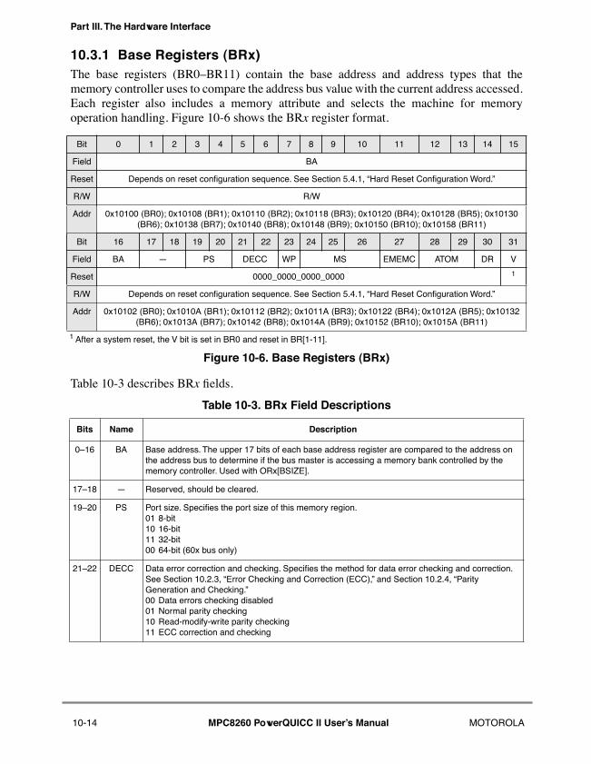
Part III. The Hardware Interface
10.3.1 Base Registers (BRx)The base registers (BR0ÐBR11) contain the base address and address types that thememory controller uses to compare the address bus value with the current address accessed.Each register also includes a memory attribute and selects the machine for memoryoperation handling. Figure 10-6 shows the BRx register format.
Table 10-3 describes BRx Þelds.
Bit 0 1 2 3 4 5 6 7 8 9 10 11 12 13 14 15
Field BA
Reset Depends on reset conÞguration sequence. See Section 5.4.1, ÒHard Reset ConÞguration Word.Ó
R/W R/W
Addr 0x10100 (BR0); 0x10108 (BR1); 0x10110 (BR2); 0x10118 (BR3); 0x10120 (BR4); 0x10128 (BR5); 0x10130 (BR6); 0x10138 (BR7); 0x10140 (BR8); 0x10148 (BR9); 0x10150 (BR10); 0x10158 (BR11)
Bit 16 17 18 19 20 21 22 23 24 25 26 27 28 29 30 31
Field BA Ñ PS DECC WP MS EMEMC ATOM DR V
Reset 0000_0000_0000_0000 1
R/W Depends on reset conÞguration sequence. See Section 5.4.1, ÒHard Reset ConÞguration Word.Ó
Addr 0x10102 (BR0); 0x1010A (BR1); 0x10112 (BR2); 0x1011A (BR3); 0x10122 (BR4); 0x1012A (BR5); 0x10132 (BR6); 0x1013A (BR7); 0x10142 (BR8); 0x1014A (BR9); 0x10152 (BR10); 0x1015A (BR11)
1 After a system reset, the V bit is set in BR0 and reset in BR[1-11].
Figure 10-6. Base Registers (BRx)
Table 10-3. BRx Field Descriptions
Bits Name Description
0Ð16 BA Base address. The upper 17 bits of each base address register are compared to the address on the address bus to determine if the bus master is accessing a memory bank controlled by the memory controller. Used with ORx[BSIZE].
17Ð18 Ñ Reserved, should be cleared.
19Ð20 PS Port size. SpeciÞes the port size of this memory region. 01 8-bit 10 16-bit 11 32-bit 00 64-bit (60x bus only)
21Ð22 DECC Data error correction and checking. SpeciÞes the method for data error checking and correction. See Section 10.2.3, ÒError Checking and Correction (ECC),Ó and Section 10.2.4, ÒParity Generation and Checking.Ó00 Data errors checking disabled01 Normal parity checking10 Read-modify-write parity checking11 ECC correction and checking
10-14 MPC8260 PowerQUICC II UserÕs Manual MOTOROLA
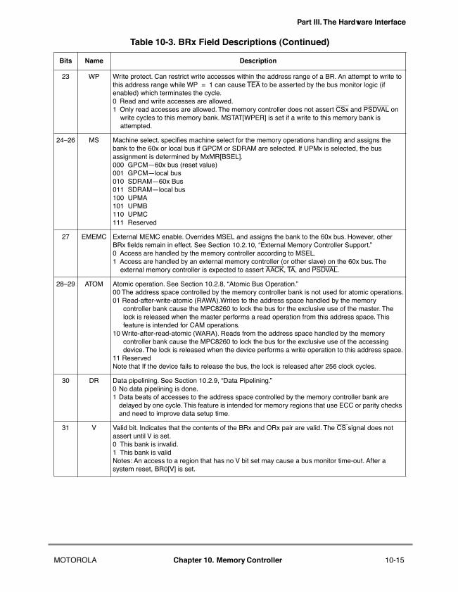
Part III. The Hardware Interface
23 WP Write protect. Can restrict write accesses within the address range of a BR. An attempt to write to this address range while WP = 1 can cause TEA to be asserted by the bus monitor logic (if enabled) which terminates the cycle. 0 Read and write accesses are allowed.1 Only read accesses are allowed. The memory controller does not assert CSx and PSDVAL on
write cycles to this memory bank. MSTAT[WPER] is set if a write to this memory bank is attempted.
24Ð26 MS Machine select. speciÞes machine select for the memory operations handling and assigns the bank to the 60x or local bus if GPCM or SDRAM are selected. If UPMx is selected, the bus assignment is determined by MxMR[BSEL].000 GPCMÑ60x bus (reset value)001 GPCMÑlocal bus010 SDRAMÑ60x Bus011 SDRAMÑlocal bus100 UPMA101 UPMB110 UPMC111 Reserved
27 EMEMC External MEMC enable. Overrides MSEL and assigns the bank to the 60x bus. However, other BRx Þelds remain in effect. See Section 10.2.10, ÒExternal Memory Controller Support.Ó0 Access are handled by the memory controller according to MSEL.1 Access are handled by an external memory controller (or other slave) on the 60x bus. The
external memory controller is expected to assert AACK, TA, and PSDVAL.
28Ð29 ATOM Atomic operation. See Section 10.2.8, ÒAtomic Bus Operation.Ó00 The address space controlled by the memory controller bank is not used for atomic operations.01 Read-after-write-atomic (RAWA).Writes to the address space handled by the memory
controller bank cause the MPC8260 to lock the bus for the exclusive use of the master. The lock is released when the master performs a read operation from this address space. This feature is intended for CAM operations.
10 Write-after-read-atomic (WARA). Reads from the address space handled by the memory controller bank cause the MPC8260 to lock the bus for the exclusive use of the accessing device. The lock is released when the device performs a write operation to this address space.
11 ReservedNote that If the device fails to release the bus, the lock is released after 256 clock cycles.
30 DR Data pipelining. See Section 10.2.9, ÒData Pipelining.Ó0 No data pipelining is done.1 Data beats of accesses to the address space controlled by the memory controller bank are
delayed by one cycle. This feature is intended for memory regions that use ECC or parity checks and need to improve data setup time.
31 V Valid bit. Indicates that the contents of the BRx and ORx pair are valid. The CS signal does not assert until V is set. 0 This bank is invalid.1 This bank is validNotes: An access to a region that has no V bit set may cause a bus monitor time-out. After a system reset, BR0[V] is set.
Table 10-3. BRx Field Descriptions (Continued)
Bits Name Description
MOTOROLA Chapter 10. Memory Controller 10-15
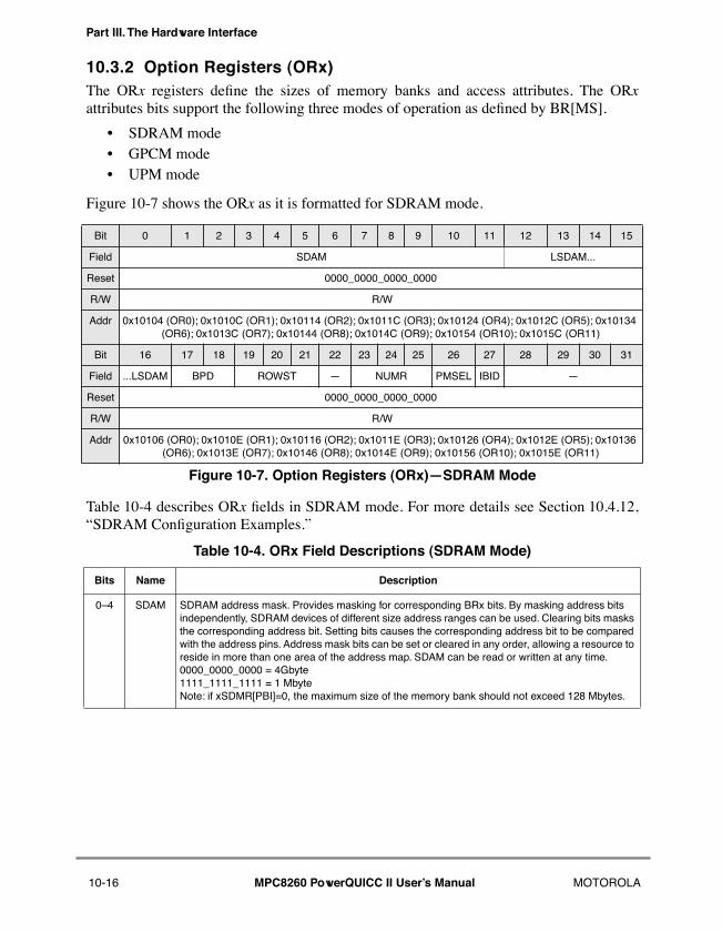
Part III. The Hardware Interface
10.3.2 Option Registers (ORx)The ORx registers deÞne the sizes of memory banks and access attributes. The ORxattributes bits support the following three modes of operation as deÞned by BR[MS].
¥ SDRAM mode¥ GPCM mode¥ UPM mode
Figure 10-7 shows the ORx as it is formatted for SDRAM mode.
Table 10-4 describes ORx Þelds in SDRAM mode. For more details see Section 10.4.12,ÒSDRAM ConÞguration Examples.Ó
Bit 0 1 2 3 4 5 6 7 8 9 10 11 12 13 14 15
Field SDAM LSDAM...
Reset 0000_0000_0000_0000
R/W R/W
Addr 0x10104 (OR0); 0x1010C (OR1); 0x10114 (OR2); 0x1011C (OR3); 0x10124 (OR4); 0x1012C (OR5); 0x10134 (OR6); 0x1013C (OR7); 0x10144 (OR8); 0x1014C (OR9); 0x10154 (OR10); 0x1015C (OR11)
Bit 16 17 18 19 20 21 22 23 24 25 26 27 28 29 30 31
Field ...LSDAM BPD ROWST Ñ NUMR PMSEL IBID Ñ
Reset 0000_0000_0000_0000
R/W R/W
Addr 0x10106 (OR0); 0x1010E (OR1); 0x10116 (OR2); 0x1011E (OR3); 0x10126 (OR4); 0x1012E (OR5); 0x10136 (OR6); 0x1013E (OR7); 0x10146 (OR8); 0x1014E (OR9); 0x10156 (OR10); 0x1015E (OR11)
Figure 10-7. Option Registers (ORx)ÑSDRAM Mode
Table 10-4. ORx Field Descriptions (SDRAM Mode)
Bits Name Description
0Ð4 SDAM SDRAM address mask. Provides masking for corresponding BRx bits. By masking address bits independently, SDRAM devices of different size address ranges can be used. Clearing bits masks the corresponding address bit. Setting bits causes the corresponding address bit to be compared with the address pins. Address mask bits can be set or cleared in any order, allowing a resource to reside in more than one area of the address map. SDAM can be read or written at any time.0000_0000_0000 = 4Gbyte1111_1111_1111 = 1 MbyteNote: if xSDMR[PBI]=0, the maximum size of the memory bank should not exceed 128 Mbytes.
10-16 MPC8260 PowerQUICC II UserÕs Manual MOTOROLA
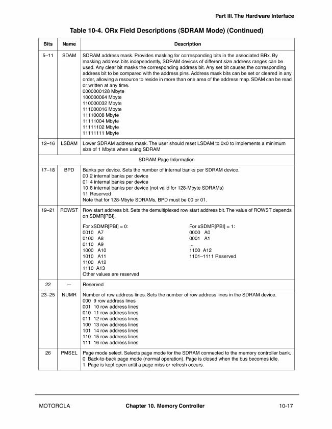
Part III. The Hardware Interface
5Ð11 SDAM SDRAM address mask. Provides masking for corresponding bits in the associated BRx. By masking address bits independently, SDRAM devices of different size address ranges can be used. Any clear bit masks the corresponding address bit. Any set bit causes the corresponding address bit to be compared with the address pins. Address mask bits can be set or cleared in any order, allowing a resource to reside in more than one area of the address map. SDAM can be read or written at any time.0000000128 Mbyte100000064 Mbyte110000032 Mbyte111000016 Mbyte11110008 Mbyte11111004 Mbyte11111102 Mbyte11111111 Mbyte
12Ð16 LSDAM Lower SDRAM address mask. The user should reset LSDAM to 0x0 to implements a minimum size of 1 Mbyte when using SDRAM
SDRAM Page Information
17Ð18 BPD Banks per device. Sets the number of internal banks per SDRAM device.00 2 internal banks per device01 4 internal banks per device10 8 internal banks per device (not valid for 128-Mbyte SDRAMs)11 ReservedNote that for 128-Mbyte SDRAMs, BPD must be 00 or 01.
19Ð21 ROWST Row start address bit. Sets the demultiplexed row start address bit. The value of ROWST depends on SDMR[PBI].
For xSDMR[PBI] = 0:0010 A70100 A80110 A91000 A101010 A111100 A121110 A13 Other values are reserved
For xSDMR[PBI] = 1:0000 A00001 A1...1100 A121101Ð1111 Reserved
22 Ñ Reserved
23Ð25 NUMR Number of row address lines. Sets the number of row address lines in the SDRAM device.000 9 row address lines001 10 row address lines010 11 row address lines011 12 row address lines100 13 row address lines101 14 row address lines110 15 row address lines111 16 row address lines
26 PMSEL Page mode select. Selects page mode for the SDRAM connected to the memory controller bank. 0 Back-to-back page mode (normal operation). Page is closed when the bus becomes idle.1 Page is kept open until a page miss or refresh occurs.
Table 10-4. ORx Field Descriptions (SDRAM Mode) (Continued)
Bits Name Description
MOTOROLA Chapter 10. Memory Controller 10-17
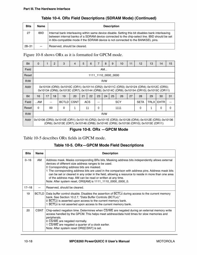
Part III. The Hardware Interface
Figure 10-8 shows ORx as it is formatted for GPCM mode.
Table 10-5 describes ORx Þelds in GPCM mode.
27 IBID Internal bank interleaving within same device disable. Setting this bit disables bank interleaving between internal banks of a SDRAM device connected to the chip-select line. IBID should be set in 60x-compatible mode if the SDRAM device is not connected to the BANKSEL pins.
28Ð31 Ñ Reserved, should be cleared.
Bit 0 1 2 3 4 5 6 7 8 9 10 11 12 13 14 15
Field AM...
Reset 1111_1110_0000_0000
R/W R/W
Addr 0x10104 (OR0); 0x1010C (OR1); 0x10114 (OR2); 0x1011C (OR3); 0x10124 (OR4); 0x1012C (OR5); 0x10134 (OR6); 0x1013C (OR7); 0x10144 (OR8); 0x1014C (OR9); 0x10154 (OR10); 0x1015C (OR11)
Bit 16 17 18 19 20 21 22 23 24 25 26 27 28 29 30 31
Field ...AM Ñ BCTLD CSNT ACS Ñ SCY SETA TRLX EHTR Ñ
Reset 0 00 0 1 11 0 1111 0 1 0 0
R/W R/W
Addr 0x10106 (OR0); 0x1010E (OR1); 0x10116 (OR2); 0x1011E (OR3); 0x10126 (OR4); 0x1012E (OR5); 0x10136 (OR6); 0x1013E (OR7); 0x10146 (OR8); 0x1014E (OR9); 0x10156 (OR10); 0x1015E (OR11)
Figure 10-8. ORx ÑGPCM Mode
Table 10-5. ORxÑGPCM Mode Field Descriptions
Bits Name Description
0Ð16 AM Address mask. Masks corresponding BRx bits. Masking address bits independently allows external devices of different size address ranges to be used. 0 Corresponding address bits are masked. 1 The corresponding address bits are used in the comparison with address pins. Address mask bits
can be set or cleared in any order in the Þeld, allowing a resource to reside in more than one area of the address map. AM can be read or written at any time.
Note: After system reset, OR0[AM] is 1111_1110_0000_0000_0.
17Ð18 Ñ Reserved, should be cleared.
19 BCTLD Data buffer control disable. Disables the assertion of BCTLx during access to the current memory bank. See Section 10.2.7, ÒData Buffer Controls (BCTLx).Ó0 BCTLx is asserted upon access to the current memory bank. 1 BCTLx is not asserted upon access to the current memory bank.
20 CSNT Chip-select negation time. Determines when CS/WE are negated during an external memory write access handled by the GPCM. This helps meet address/data hold times for slow memories and peripherals.0 CS/WE are negated normally. 1 CS/WE are negated a quarter of a clock earlier.Note: After system reset OR0[CSNT] is set.
Table 10-4. ORx Field Descriptions (SDRAM Mode) (Continued)
Bits Name Description
10-18 MPC8260 PowerQUICC II UserÕs Manual MOTOROLA
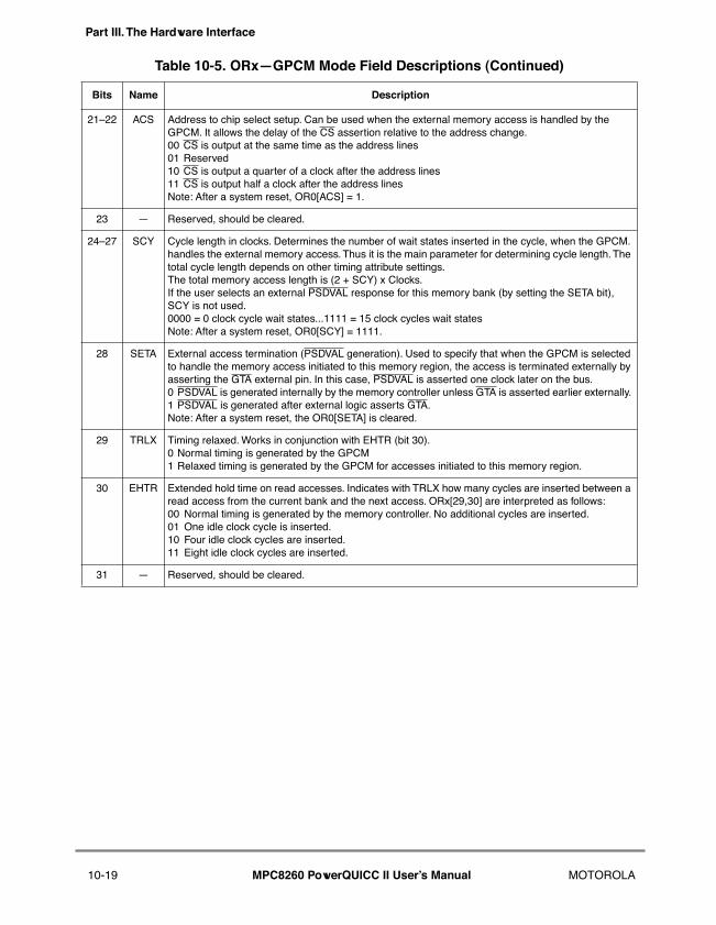
Part III. The Hardware Interface
21Ð22 ACS Address to chip select setup. Can be used when the external memory access is handled by the GPCM. It allows the delay of the CS assertion relative to the address change.00 CS is output at the same time as the address lines 01 Reserved10 CS is output a quarter of a clock after the address lines11 CS is output half a clock after the address linesNote: After a system reset, OR0[ACS] = 1.
23 Ñ Reserved, should be cleared.
24Ð27 SCY Cycle length in clocks. Determines the number of wait states inserted in the cycle, when the GPCM. handles the external memory access. Thus it is the main parameter for determining cycle length. The total cycle length depends on other timing attribute settings.The total memory access length is (2 + SCY) x Clocks.If the user selects an external PSDVAL response for this memory bank (by setting the SETA bit), SCY is not used.0000 = 0 clock cycle wait states...1111 = 15 clock cycles wait statesNote: After a system reset, OR0[SCY] = 1111.
28 SETA External access termination (PSDVAL generation). Used to specify that when the GPCM is selected to handle the memory access initiated to this memory region, the access is terminated externally by asserting the GTA external pin. In this case, PSDVAL is asserted one clock later on the bus.0 PSDVAL is generated internally by the memory controller unless GTA is asserted earlier externally. 1 PSDVAL is generated after external logic asserts GTA.Note: After a system reset, the OR0[SETA] is cleared.
29 TRLX Timing relaxed. Works in conjunction with EHTR (bit 30).0 Normal timing is generated by the GPCM1 Relaxed timing is generated by the GPCM for accesses initiated to this memory region.
30 EHTR Extended hold time on read accesses. Indicates with TRLX how many cycles are inserted between a read access from the current bank and the next access. ORx[29,30] are interpreted as follows:00 Normal timing is generated by the memory controller. No additional cycles are inserted. 01 One idle clock cycle is inserted.10 Four idle clock cycles are inserted.11 Eight idle clock cycles are inserted.
31 Ñ Reserved, should be cleared.
Table 10-5. ORxÑGPCM Mode Field Descriptions (Continued)
Bits Name Description
10-19 MPC8260 PowerQUICC II UserÕs Manual MOTOROLA
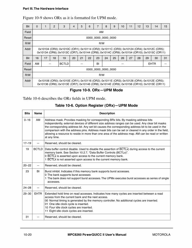
Part III. The Hardware Interface
Figure 10-9 shows ORx as it is formatted for UPM mode.
Table 10-6 describes the ORx Þelds in UPM mode.
Bit 0 1 2 3 4 5 6 7 8 9 10 11 12 13 14 15
Field AM
Reset 0000_0000_0000_0000
R/W R/W
Addr 0x10104 (OR0); 0x1010C (OR1); 0x10114 (OR2); 0x1011C (OR3); 0x10124 (OR4); 0x1012C (OR5); 0x10134 (OR6); 0x1013C (OR7); 0x10144 (OR8); 0x1014C (OR9); 0x10154 (OR10); 0x1015C (OR11)
Bit 16 17 18 19 20 21 22 23 24 25 26 27 28 29 30 31
Field AM Ñ BCTLD Ñ BI Ñ EHTR Ñ
Reset 0000_0000_0000_0000
R/W R/W
Addr 0x10106 (OR0); 0x1010E (OR1); 0x10116 (OR2); 0x1011E (OR3); 0x10126 (OR4); 0x1012E (OR5); 0x10136 (OR6); 0x1013E (OR7); 0x10146 (OR8); 0x1014E (OR9); 0x10156 (OR10); 0x1015E (OR11)
Figure 10-9. ORxÑUPM Mode
Table 10-6. Option Register (ORx)ÑUPM Mode
Bits Name Description
0Ð16 AM Address mask. Provides masking for corresponding BRx bits. By masking address bits independently, external devices of different size address ranges can be used. Any clear bit masks the corresponding address bit. Any set bit causes the corresponding address bit to be used in the comparison with the address pins. Address mask bits can be set or cleared in any order in the Þeld, allowing a resource to reside in more than one area of the address map. AM can be read or written at any time.
17Ð19 Ñ Reserved, should be cleared.
19 BCTLD Data buffer control disable. Used to disable the assertion of BCTLx) during access to the current memory bank. See Section 10.2.7, ÒData Buffer Controls (BCTLx)Ó.0 BCTLx is asserted upon access to the current memory bank. 1 BCTLx is not asserted upon access to the current memory bank.
20Ð22 Ñ Reserved, should be cleared.
23 BI Burst inhibit. Indicates if this memory bank supports burst accesses. 0 The bank supports burst accesses1 The bank does not support burst accesses. The UPMx executes burst accesses as series of single
accesses.
24Ð28 Ñ Reserved, should be cleared.
29Ð30 EHTR Extended hold time on read accesses. Indicates how many cycles are inserted between a read access from the current bank and the next access. 00 Normal timing is generated by the memory controller. No additional cycles are inserted. 01 One idle clock cycle is inserted.10 Four idle clock cycles are inserted.11 Eight idle clock cycles are inserted.
31 Ñ Reserved, should be cleared.
10-20 MPC8260 PowerQUICC II UserÕs Manual MOTOROLA
Part III. The Hardware Interface
10.3.3 60x SDRAM Mode Register (PSDMR)The 60x SDRAM mode register (PSDMR), shown in Figure 10-10, is used to conÞgureoperations pertaining to SDRAM.
Table 10-7 describes PSMDR Þelds. LSMDR Þelds are described in Table 10-8.
Bit 0 1 2 3 4 5 6 7 8 9 10 11 12 13 14 15
Field PBI RFEN OP SDAM BSMA SDA10 RFRC
Reset 0000_0000_0000_0000
R/W R/W
Addr 0x10190 (PSDMR), 0x10194 (LSDMR)
Bit 16 17 18 19 20 21 22 23 24 25 26 27 28 29 30 31
Field RFRC PRETOACT ACTTORW BL LDOTOPRE WRC EAMUX BUFCMD CL
Reset 0000_0000_0000_0000
R/W R/W
Addr 0x10192 (PSDMR), 0x10196 (LSDMR)
Figure 10-10. 60x/Local SDRAM Mode Register (PSDMR/LSDMR)
Table 10-7. PSDMR Field Descriptions
Bits Name Description
0 PBI Page-based interleaving. Selects the address multiplexing method. PBI works in conjunction with ORx[SDA10]. See Section 10.4.5, ÒBank Interleaving.Ó 0 Bank-based interleaving1 Page-based interleaving (normal operation)
1 RFEN Refresh enable. Indicates that the UPM needs refresh services.0 Refresh services are not required 1 Refresh services are requiredNote: After system reset, RFEN is cleared.See Section 10.3.8, Ò60x Bus-Assigned UPM Refresh Timer (PURT),Ó Section 10.3.9, ÒLocal Bus-Assigned UPM Refresh Timer (LURT),Ó Section 10.3.10, Ò60x Bus-Assigned SDRAM Refresh Timer (PSRT),Ó and Section 10.3.11, ÒLocal Bus-Assigned SDRAM Refresh Timer (LSRT).Ó
2Ð4 OP SDRAM operation. Determines which operation occurs when the SDRAM device is accessed. 000 Normal operation001 CBR refresh, used in SDRAM initialization.010 Self refresh (for debug purpose).011 Mode Register write, used in SDRAM initialization.Note that if 60x-compatible mode is in effect on the 60x bus, the bus master must supply the mode register data on the low bits of the address during the access.100 Precharge bank (for debug purpose).101 Precharge all banks, used in SDRAM initialization.110 Activate bank (for debug purpose).111 Read/write (for debug purpose).
5Ð7 SDAM Address multiplex size. Determines how the address of the current memory cycle can be output on the address pins. See Section 10.4.5.1, ÒSDRAM Address Multiplexing (SDAM and BSMA).Ó
MOTOROLA Chapter 10. Memory Controller 10-21
Part III. The Hardware Interface
8Ð10 BSMA Bank select multiplexed address line. Selects the address pins to serve as bank-select address for the 60x SDRAM. The bank select address can also be output on the BANKSEL pins (optional). See Section 10.4.5.1, ÒSDRAM Address Multiplexing (SDAM and BSMA).Ó000 A12ÐA14001 A13ÐA15010 A14ÐA16011 A15ÐA17100 A16ÐA18101 A17ÐA19110 A18ÐA20111 A19ÐA21
11Ð13 SDA10 ÒA10Ó control. With ORx[PBI], determines which address line can be output to SDA10 during an ACTIVATE command, when SDRAM is selected, to control the memory access. See Section 10.4.12.1, ÒSDRAM ConÞguration Example (Page-Based Interleaving).Ó
For PBI = 0:000 A12001 A11010 A10011 A9100 A8101 A7110 A6111 A5
For PBI = 1:000 A10001 A9010 A8011 A7100 A6101 A5110 A4111 A3
SDRAM DeviceÐSpeciÞc Parameters:
14Ð16 RFRC Refresh recovery. DeÞnes the earliest timing for an activate command after a REFRESH command. Sets the refresh recovery interval in clock cycles. See Section 10.4.6.6, ÒRefresh Recovery Interval (RFRC),Ó for how to set this Þeld.000 Reserved001 3 clocks010 4 clocks011 5 clocks100 6 clocks101 7 clocks110 8 clocks111 16 clocks
17Ð19 PRETOACT Precharge to activate interval. DeÞnes the earliest timing for ACTIVATE or REFRESH command after a precharge command. See Section 10.4.6.1, ÒPrecharge-to-Activate Interval.Ó001 1 clock-cycle wait states010 2 clock-cycle wait states...111 7 clock-cycle wait states000 8 clock-cycle wait states
20Ð22 ACTTORW Activate to read/write interval. DeÞnes the earliest timing for READ/WRITE command after an ACTIVATE command. See Section 10.4.6.2, ÒActivate to Read/Write Interval.Ó001 1 clock cycle 010 2 clock cycles ...111 7 clock cycles 000 8 clock cycles
Table 10-7. PSDMR Field Descriptions (Continued)
Bits Name Description
10-22 MPC8260 PowerQUICC II UserÕs Manual MOTOROLA
Part III. The Hardware Interface
23 BL Burst length0 SDRAM burst length is 4. Use this value if the device port size is 64 or 161 SDRAM burst length is 8. Use this value if the device port size is 32 or 8
24Ð25 LDOTOPRE Last data out to precharge. DeÞnes the earliest timing for PRECHARGE command after the last data was read from the SDRAM. See Section 10.4.6.4, ÒLast Data Out to Precharge.Ó00 0 clock cycles 01 -1 clock cycle10 -2 clock cycles 11 Reserved
26Ð27 WRC Write recovery time. DeÞnes the earliest timing for PRECHARGE command after the last data was written to the SDRAM. See Section 10.4.6.5, ÒLast Data In to PrechargeÑWrite Recovery.Ó01 1 clock cycles 10 2 clock cycles 11 3 clock cycles 00 4 clock cycles
28 EAMUX External address multiplexing enable/disable. 0 No external address multiplexing. Fastest timing.1 The memory controller asserts SDAMUX for an extra cycle before issuing an ACTIVATE
command to the SDRAM. This is useful when external address multiplexing can cause a delay on the address lines. Note that if this bit is set, ACTTORW should be a minimum of 2.
In 60x-compatible mode, external address multiplexing is placed on the address lines. If the additional delay of the multiplexing endangers the device setup time, EAMUX should be set. Setting this bit causes the memory controller to add another cycle for each address phase. Note that EAMUX can also be set in any case of delays on the address lines, such as address buffers. See Section 10.4.6.7, ÒExternal Address Multiplexing Signal.Ó
29 BUFCMD If external buffers are placed on the control lines going to both the SDRAM and address lines, setting BUFCMD causes all SDRAM control lines except CS to be asserted for two cycles, instead of one. See Section 10.4.6.8, ÒExternal Address and Command Buffers (BUFCMD).Ó0 Normal timing for the control lines1 All control lines except CS are asserted for two cyclesIn 60x-compatible mode, external buffers may be placed on the command strobes, except CS, as well as the address lines. If the additional delay of the buffers endangers the device setup time, BUFCMD should be set, which causes the memory controller to add a cycle for each SDRAM command.
30Ð31 CL CAS latency. DeÞnes the timing for Þrst read data after SDRAM samples a column address. See Section 10.4.6.3, ÒColumn Address to First Data OutÑCAS Latency.Ó00 Reserved 01 110 2 11 3
Table 10-7. PSDMR Field Descriptions (Continued)
Bits Name Description
MOTOROLA Chapter 10. Memory Controller 10-23
Part III. The Hardware Interface
10.3.4 Local Bus SDRAM Mode Register (LSDMR)The LSDMR, shown in Figure 10-10, has the same Þelds as the PSDMR. Table 10-8describes LSDMR Þelds.
Table 10-8. LSDMR Field Descriptions
Bits Name Description
0 PBI Page-based interleaving. Selects the address multiplexing method. PBI works in conjunction with ORx[SDA10]. See Section 10.4.5, ÒBank Interleaving.Ó 0 Bank-based interleaving1 Page-based interleaving (normal operation)
1 RFEN Refresh enable. Indicates that the SDRAM requires refresh services.0 Refresh services are not required 1 Refresh services are required
2Ð4 OP SDRAM operation. Selects the operation that occurs when the SDRAM device is accessed. 000 Normal operation001 CBR refresh, used in SDRAM initialization.010 Self refresh (for debug purpose).011 Mode Register write, used in SDRAM initialization.100 Precharge bank (for debug purpose).101 Precharge all banks, used in SDRAM initialization.110 Activate bank (for debug purpose).111 Read/write (for debug purpose).
5Ð7 SDAM Address multiplex size. Determines how the address of the current memory cycle is output on the address pins. See Section 10.4.5.1, ÒSDRAM Address Multiplexing (SDAM and BSMA).Ó
8Ð10 BSMA Bank select multiplexed address line. Selects which MPC8260 address pins serve as bank-select address for the local bus SDRAM. See Section 10.4.5.1, ÒSDRAM Address Multiplexing (SDAM and BSMA).Ó000 L_A14 (ORx[BPD] must be 00)001 L_AÐL_A15 (ORx[BPD] must be 00 or 01)010 L_A14ÐL_A16011 L_A15ÐL_A17100 L_A16ÐL_A18101 L_A17ÐL_A19110 L_A18ÐL_A20111 L_A19ÐL_A21
11Ð13 SDA10 ÒA10Ó control. When SDRAM is selected, with ORx[PBI], determines which address line is output to SDA10 during an ACTIVATE command, to control the memory access. See Section 10.4.12.1, ÒSDRAM ConÞguration Example (Page-Based Interleaving).Ó
For PBI=0:000 A12001 A11010 A10011 A9100 A8101 A7110 A6111 A5
For PBI=1:000 A10001 A9010 A8011 A7100 A6101 A5110 A4111 A3
10-24 MPC8260 PowerQUICC II UserÕs Manual MOTOROLA
Part III. The Hardware Interface
SDRAM DeviceÐSpeciÞc Parameters:
14Ð16 RFRC Refresh recovery. DeÞnes the earliest timing for an activate command after a REFRESH command. Sets the refresh recovery interval in clock cycles. See Section 10.4.6.6, ÒRefresh Recovery Interval (RFRC),Ó for how to set this Þeld.000 Reserved001 3 clocks010 4 clocks011 5 clocks100 6 clocks101 7 clocks110 8 clocks111 16 clocks
17Ð19 PRETOACT Precharge to activate interval. DeÞnes the earliest timing for ACTIVATE or REFRESH command after a precharge command. See Section 10.4.6.1, ÒPrecharge-to-Activate Interval.Ó001 1 clock-cycle wait states010 2 clock-cycle wait states...111 7 clock-cycle wait states000 8 clock-cycle wait states
20Ð22 ACTTORW Activate to read/write interval. DeÞnes the earliest timing for READ/WRITE command after an ACTIVATE command. See Section 10.4.6.2, ÒActivate to Read/Write Interval.Ó001 1 clock cycle 010 2 clock cycles ...111 7 clock cycles 000 8 clock cycles
23 BL Burst length0 SDRAM burst length is 4. Use this value if the device port size is161 SDRAM burst length is 8. Use this value if the device port size is 32 or 8
24Ð25 LDOTOPRE Last data out to precharge. DeÞnes the earliest timing for PRECHARGE command after the last data was read from the SDRAM. See Section 10.4.6.4, ÒLast Data Out to Precharge.Ó00 0 clock cycles 01 -1 clock cycle10 -2 clock cycles 11 Reserved
26Ð27 WRC Write recovery time. DeÞnes the earliest timing for PRECHARGE command after the last data is written to the SDRAM. See Section 10.4.6.5, ÒLast Data In to PrechargeÑWrite Recovery.Ó01 1 clock cycles 10 2 clock cycles 11 3 clock cycles 00 4 clock cycles
Table 10-8. LSDMR Field Descriptions (Continued)
Bits Name Description
MOTOROLA Chapter 10. Memory Controller 10-25
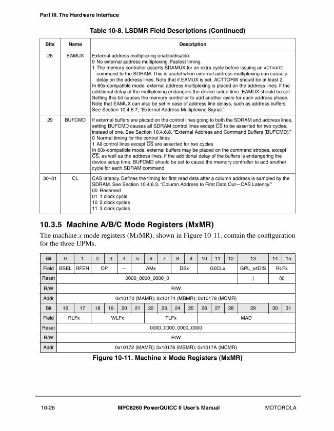
Part III. The Hardware Interface
10.3.5 Machine A/B/C Mode Registers (MxMR)The machine x mode registers (MxMR), shown in Figure 10-11, contain the conÞgurationfor the three UPMs.
28 EAMUX External address multiplexing enable/disable.0 No external address multiplexing. Fastest timing.1 The memory controller asserts SDAMUX for an extra cycle before issuing an ACTIVATE
command to the SDRAM. This is useful when external address multiplexing can cause a delay on the address lines. Note that if EAMUX is set, ACTTORW should be at least 2.
In 60x-compatible mode, external address multiplexing is placed on the address lines. If the additional delay of the multiplexing endangers the device setup time, EAMUX should be set. Setting this bit causes the memory controller to add another cycle for each address phase. Note that EAMUX can also be set in case of address line delays, such as address buffers.See Section 10.4.6.7, ÒExternal Address Multiplexing Signal.Ó
29 BUFCMD If external buffers are placed on the control lines going to both the SDRAM and address lines, setting BUFCMD causes all SDRAM control lines except CS to be asserted for two cycles, instead of one. See Section 10.4.6.8, ÒExternal Address and Command Buffers (BUFCMD).Ó0 Normal timing for the control lines1 All control lines except CS are asserted for two cyclesIn 60x-compatible mode, external buffers may be placed on the command strobes, except CS, as well as the address lines. If the additional delay of the buffers is endangering the device setup time, BUFCMD should be set to cause the memory controller to add another cycle for each SDRAM command.
30Ð31 CL CAS latency. DeÞnes the timing for Þrst read data after a column address is sampled by the SDRAM. See Section 10.4.6.3, ÒColumn Address to First Data OutÑCAS Latency.Ó00 Reserved 01 1 clock cycle10 2 clock cycles11 3 clock cycles
Bit 0 1 2 3 4 5 6 7 8 9 10 11 12 13 14 15
Field BSEL RFEN OP Ñ AMx DSx G0CLx GPL_x4DIS RLFx
Reset 0000_0000_0000_0 1 00
R/W R/W
Addr 0x10170 (MAMR); 0x10174 (MBMR); 0x10178 (MCMR)
Bit 16 17 18 19 20 21 22 23 24 25 26 27 28 29 30 31
Field RLFx WLFx TLFx MAD
Reset 0000_0000_0000_0000
R/W R/W
Addr 0x10172 (MAMR); 0x10176 (MBMR); 0x1017A (MCMR)
Figure 10-11. Machine x Mode Registers (MxMR)
Table 10-8. LSDMR Field Descriptions (Continued)
Bits Name Description
10-26 MPC8260 PowerQUICC II UserÕs Manual MOTOROLA
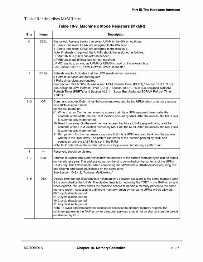
Part III. The Hardware Interface
Table 10-9 describes MxMR bits.
Table 10-9. Machine x Mode Registers (MxMR)
Bits Name Description
0 BSEL Bus select. Assigns banks that select UPMx to the 60x or local bus.0 Banks that select UPMx are assigned to the 60x bus.1 Banks that select UPMx are assigned to the local bus.Note: if refresh is required, the UPMÕs should be assigned as follows:UPMA: 60x bus (if 60x bus refresh needed)UPMB: Local bus (if local bus refresh required)UPMC: any bus, as long as UPMA or UPMB is used on the relevant bus. See Section 10.6.1.2, ÒUPM Refresh Timer Requests.Ó
1 RFEN Refresh enable. Indicates that the UPM needs refresh services.0 Refresh services are not required 1 Refresh services are requiredSee Section 10.3.8, Ò60x Bus-Assigned UPM Refresh Timer (PURT),Ó Section 10.3.9, ÒLocal Bus-Assigned UPM Refresh Timer (LURT),Ó Section 10.3.10, Ò60x Bus-Assigned SDRAM Refresh Timer (PSRT),Ó and Section 10.3.11, ÒLocal Bus-Assigned SDRAM Refresh Timer (LSRT).Ó
2Ð3 OP Command opcode. Determines the command executed by the UPMx when a memory access hit a UPM assigned bank.00 Normal operation.01 Write to array. On the next memory access that hits a UPM assigned bank, write the
contents of the MDR into the RAM location pointed by MAD. After the access, the MAD Þeld is automatically incremented.
10 Read from array. On the next memory access that hits a UPM assigned bank, read the contents of the RAM location pointed by MAD into the MDR. After the access, the MAD Þeld is automatically incremented
11 Run pattern. On the next memory access that hits a UPM assigned bank, run the pattern written in the RAM array. The pattern run starts at the location pointed by MAD and continues until the LAST bit is set in the RAM.
Note: RLF determines the number of times a loop is executed during a pattern run.
4 Ñ Reserved, should be cleared.
5Ð7 AMx Address multiplex size. Determines how the address of the current memory cycle can be output on the address pins. The address output on the pins controlled by the contents of the UPMx RAM array. This Þeld is useful when connecting the MPC8260 to DRAM devices requiring row and column addresses multiplexed on the same pins.See Section 10.6.4.2, ÒAddress Multiplexing.Ó
8Ð9 DSx Disable timer period. Guarantees a minimum time between accesses to the same memory bank if it is controlled by the UPMx. The disable timer is turned on by the TODT in the RAM array, and when expired, the UPMx allows the machine access to handle a memory pattern to the same memory region. Accesses to a different memory region by the same UPMx will be allowed.00 1-cycle disable period01 2-cycle disable period10 3-cycle disable period11 4-cycle disable periodNote: To avoid conßicts between successive accesses to different memory regions, the minimum pattern in the RAM array for a request serviced should not be shorter than the period established by DSx.
MOTOROLA Chapter 10. Memory Controller 10-27
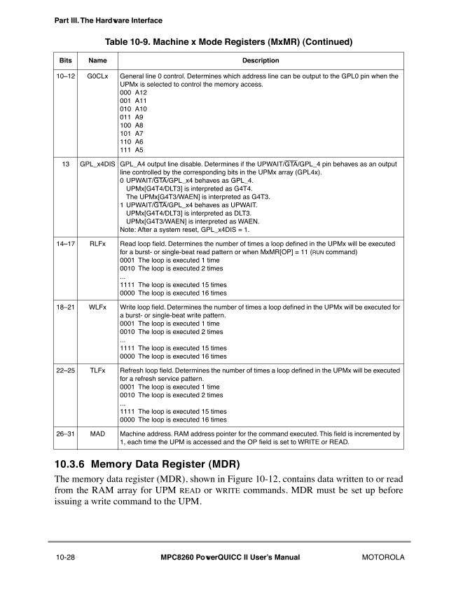
Part III. The Hardware Interface
10.3.6 Memory Data Register (MDR)The memory data register (MDR), shown in Figure 10-12, contains data written to or readfrom the RAM array for UPM READ or WRITE commands. MDR must be set up beforeissuing a write command to the UPM.
10Ð12 G0CLx General line 0 control. Determines which address line can be output to the GPL0 pin when the UPMx is selected to control the memory access.000 A12001 A11010 A10011 A9100 A8101 A7110 A6111 A5
13 GPL_x4DIS GPL_A4 output line disable. Determines if the UPWAIT/GTA/GPL_4 pin behaves as an output line controlled by the corresponding bits in the UPMx array (GPL4x). 0 UPWAIT/GTA/GPL_x4 behaves as GPL_4.
UPMx[G4T4/DLT3] is interpreted as G4T4.The UPMx[G4T3/WAEN] is interpreted as G4T3.
1 UPWAIT/GTA/GPL_x4 behaves as UPWAIT.UPMx[G4T4/DLT3] is interpreted as DLT3.UPMx[G4T3/WAEN] is interpreted as WAEN.
Note: After a system reset, GPL_x4DIS = 1.
14Ð17 RLFx Read loop Þeld. Determines the number of times a loop deÞned in the UPMx will be executed for a burst- or single-beat read pattern or when MxMR[OP] = 11 (RUN command)0001 The loop is executed 1 time0010 The loop is executed 2 times...1111 The loop is executed 15 times0000 The loop is executed 16 times
18Ð21 WLFx Write loop Þeld. Determines the number of times a loop deÞned in the UPMx will be executed for a burst- or single-beat write pattern.0001 The loop is executed 1 time0010 The loop is executed 2 times...1111 The loop is executed 15 times0000 The loop is executed 16 times
22Ð25 TLFx Refresh loop Þeld. Determines the number of times a loop deÞned in the UPMx will be executed for a refresh service pattern.0001 The loop is executed 1 time0010 The loop is executed 2 times...1111 The loop is executed 15 times0000 The loop is executed 16 times
26Ð31 MAD Machine address. RAM address pointer for the command executed. This Þeld is incremented by 1, each time the UPM is accessed and the OP Þeld is set to WRITE or READ.
Table 10-9. Machine x Mode Registers (MxMR) (Continued)
Bits Name Description
10-28 MPC8260 PowerQUICC II UserÕs Manual MOTOROLA
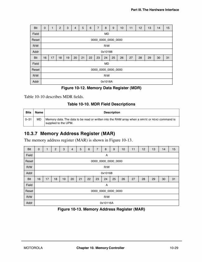
Part III. The Hardware Interface
Table 10-10 describes MDR Þelds.
10.3.7 Memory Address Register (MAR)The memory address register (MAR) is shown in Figure 10-13.
Bit 0 1 2 3 4 5 6 7 8 9 10 11 12 13 14 15
Field MD
Reset 0000_0000_0000_0000
R/W R/W
Addr 0x10188
Bit 16 17 18 19 20 21 22 23 24 25 26 27 28 29 30 31
Field MD
Reset 0000_0000_0000_0000
R/W R/W
Addr 0x1018A
Figure 10-12. Memory Data Register (MDR)
Table 10-10. MDR Field Descriptions
Bits Name Description
0Ð31 MD Memory data. The data to be read or written into the RAM array when a WRITE or READ command is supplied to the UPM.
Bit 0 1 2 3 4 5 6 7 8 9 10 11 12 13 14 15
Field A
Reset 0000_0000_0000_0000
R/W R/W
Addr 0x10168
Bit 16 17 18 19 20 21 22 23 24 25 26 27 28 29 30 31
Field A
Reset 0000_0000_0000_0000
R/W R/W
Addr 0x10116A
Figure 10-13. Memory Address Register (MAR)
MOTOROLA Chapter 10. Memory Controller 10-29
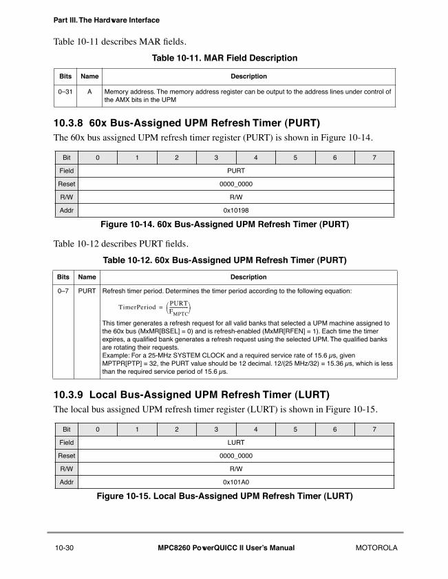
Part III. The Hardware Interface
Table 10-11 describes MAR Þelds.
10.3.8 60x Bus-Assigned UPM Refresh Timer (PURT)The 60x bus assigned UPM refresh timer register (PURT) is shown in Figure 10-14.
Table 10-12 describes PURT Þelds.
10.3.9 Local Bus-Assigned UPM Refresh Timer (LURT)The local bus assigned UPM refresh timer register (LURT) is shown in Figure 10-15.
Table 10-11. MAR Field Description
Bits Name Description
0Ð31 A Memory address. The memory address register can be output to the address lines under control of the AMX bits in the UPM
Bit 0 1 2 3 4 5 6 7
Field PURT
Reset 0000_0000
R/W R/W
Addr 0x10198
Figure 10-14. 60x Bus-Assigned UPM Refresh Timer (PURT)
Table 10-12. 60x Bus-Assigned UPM Refresh Timer (PURT)
Bits Name Description
0Ð7 PURT Refresh timer period. Determines the timer period according to the following equation:
This timer generates a refresh request for all valid banks that selected a UPM machine assigned to the 60x bus (MxMR[BSEL] = 0) and is refresh-enabled (MxMR[RFEN] = 1). Each time the timer expires, a qualiÞed bank generates a refresh request using the selected UPM. The qualiÞed banks are rotating their requests. Example: For a 25-MHz SYSTEM CLOCK and a required service rate of 15.6 µs, given MPTPR[PTP] = 32, the PURT value should be 12 decimal. 12/(25 MHz/32) = 15.36 µs, which is less than the required service period of 15.6 µs.
Bit 0 1 2 3 4 5 6 7
Field LURT
Reset 0000_0000
R/W R/W
Addr 0x101A0
Figure 10-15. Local Bus-Assigned UPM Refresh Timer (LURT)
TimerPeriodPURTFMPTC-----------------è ø
æ ö=
10-30 MPC8260 PowerQUICC II UserÕs Manual MOTOROLA
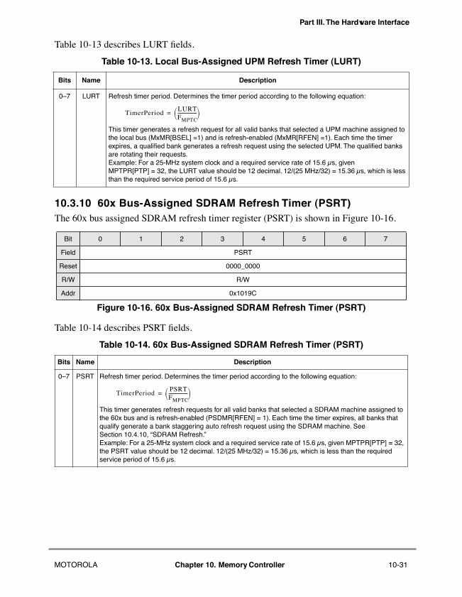
Part III. The Hardware Interface
Table 10-13 describes LURT Þelds.
10.3.10 60x Bus-Assigned SDRAM Refresh Timer (PSRT)The 60x bus assigned SDRAM refresh timer register (PSRT) is shown in Figure 10-16.
Table 10-14 describes PSRT Þelds.
Table 10-13. Local Bus-Assigned UPM Refresh Timer (LURT)
Bits Name Description
0Ð7 LURT Refresh timer period. Determines the timer period according to the following equation:
This timer generates a refresh request for all valid banks that selected a UPM machine assigned to the local bus (MxMR[BSEL] =1) and is refresh-enabled (MxMR[RFEN] =1). Each time the timer expires, a qualiÞed bank generates a refresh request using the selected UPM. The qualiÞed banks are rotating their requests.Example: For a 25-MHz system clock and a required service rate of 15.6 µs, given MPTPR[PTP] = 32, the LURT value should be 12 decimal. 12/(25 MHz/32) = 15.36 µs, which is less than the required service period of 15.6 µs.
Bit 0 1 2 3 4 5 6 7
Field PSRT
Reset 0000_0000
R/W R/W
Addr 0x1019C
Figure 10-16. 60x Bus-Assigned SDRAM Refresh Timer (PSRT)
Table 10-14. 60x Bus-Assigned SDRAM Refresh Timer (PSRT)
Bits Name Description
0Ð7 PSRT Refresh timer period. Determines the timer period according to the following equation:
This timer generates refresh requests for all valid banks that selected a SDRAM machine assigned to the 60x bus and is refresh-enabled (PSDMR[RFEN] = 1). Each time the timer expires, all banks that qualify generate a bank staggering auto refresh request using the SDRAM machine. See Section 10.4.10, ÒSDRAM Refresh.ÓExample: For a 25-MHz system clock and a required service rate of 15.6 µs, given MPTPR[PTP] = 32, the PSRT value should be 12 decimal. 12/(25 MHz/32) = 15.36 µs, which is less than the required service period of 15.6 µs.
TimerPeriodLURTFMPTC-----------------è ø
æ ö=
TimerPeriodPSRTFMPTC-----------------è ø
æ ö=
MOTOROLA Chapter 10. Memory Controller 10-31
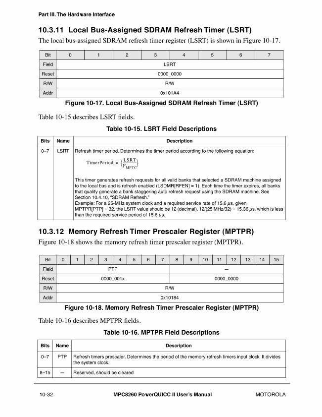
Part III. The Hardware Interface
10.3.11 Local Bus-Assigned SDRAM Refresh Timer (LSRT)The local bus-assigned SDRAM refresh timer register (LSRT) is shown in Figure 10-17.
Table 10-15 describes LSRT Þelds.
10.3.12 Memory Refresh Timer Prescaler Register (MPTPR)Figure 10-18 shows the memory refresh timer prescaler register (MPTPR).
Table 10-16 describes MPTPR Þelds.
Bit 0 1 2 3 4 5 6 7
Field LSRT
Reset 0000_0000
R/W R/W
Addr 0x101A4
Figure 10-17. Local Bus-Assigned SDRAM Refresh Timer (LSRT)
Table 10-15. LSRT Field Descriptions
Bits Name Description
0Ð7 LSRT Refresh timer period. Determines the timer period according to the following equation:
This timer generates refresh requests for all valid banks that selected a SDRAM machine assigned to the local bus and is refresh enabled (LSDMR[RFEN] = 1). Each time the timer expires, all banks that qualify generate a bank staggering auto refresh request using the SDRAM machine. See Section 10.4.10, ÒSDRAM Refresh.Ó Example: For a 25-MHz system clock and a required service rate of 15.6 µs, given MPTPR[PTP] = 32, the LSRT value should be 12 (decimal). 12/(25 MHz/32) = 15.36 µs, which is less than the required service period of 15.6 µs.
Bit 0 1 2 3 4 5 6 7 8 9 10 11 12 13 14 15
Field PTP Ñ
Reset 0000_001x 0000_0000
R/W R/W
Addr 0x10184
Figure 10-18. Memory Refresh Timer Prescaler Register (MPTPR)
Table 10-16. MPTPR Field Descriptions
Bits Name Description
0Ð7 PTP Refresh timers prescaler. Determines the period of the memory refresh timers input clock. It divides the system clock.
8Ð15 Ñ Reserved, should be cleared
TimerPeriodLSRTFMPTC-----------------è ø
æ ö=
10-32 MPC8260 PowerQUICC II UserÕs Manual MOTOROLA
Part III. The Hardware Interface
10.3.13 60x Bus Error Status and Control Registers (TESCRx)These registers indicate the source of an error that caused TEA or MCP to be asserted onthe 60x bus. See Section 4.3.2.10, Ò60x Bus Transfer Error Status and Control Register 1(TESCR1),Ó and Section 4.3.2.11, Ò60x Bus Transfer Error Status and Control Register 2(TESCR2).Ó
10.3.14 Local Bus Error Status and Control Registers (L_TESCRx)These registers indicate the source of an error that causes TEA or MCP to be asserted onthe local bus. See Section 4.3.2.12, ÒLocal Bus Transfer Error Status and Control Register 1(L_TESCR1),Ó and Section 4.3.2.13, ÒLocal Bus Transfer Error Status and ControlRegister 2 (L_TESCR2).Ó
10.4 SDRAM MachineThe MPC8260 provides one SDRAM interface (machine) for the 60x bus and one for thelocal bus. The machines provide the necessary control functions and signals forJEDEC-compliant SDRAM devices.
Each bank can control a SDRAM device on the 60x or the local bus. Table 10-17 describesthe SDRAM interface signals controlled by the memory controller.
Additional controls are available in 60x-compatible mode (60x bus only):
¥ ALEÑExternal address latch enable
¥ PSDAMUXÑExternal address multiplexing control (asserted = row, negated = column)
¥ BNKSEL[0Ð2]ÑBank select address to allow internal bank interleaving
Throughout this section, whenever a signal is named, the reference is to the 60x or local bussignal, according to the accessed bankÕs machine-select.
Figure 10-19 shows an eight-bank, 128-Mbyte system. Each bank consists of eight 2 x1-Mbit x 8 SDRAMs. Note that the SDRAM memory clock must operate at the samefrequency as, and be phase-aligned with, the system clock.
Table 10-17. SDRAM Interface Signals
60x Bus Local Bus Comments
CS[0Ð11] Device select
PSDRAS LSDRAS RAS
SDCAS LSDCAS CAS
SDWE LSDWE WEN
SDA10 LSDA10 ÒA10Ó control
DQM[0Ð7] LDQM[0Ð3] Byte select
MOTOROLA Chapter 10. Memory Controller 10-33
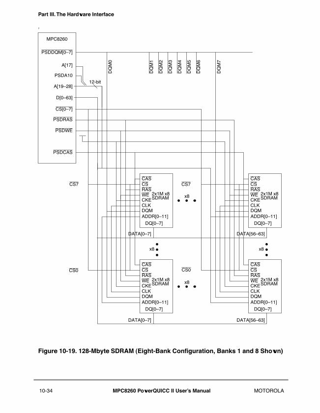
Part III. The Hardware Interface
y
Figure 10-19. 128-Mbyte SDRAM (Eight-Bank Configuration, Banks 1 and 8 Shown)
CKECLKDQMADDR[0Ð11]
DQ[0Ð7]
DATA[0Ð7] DATA[56Ð63]
DATA[0Ð7] DATA[56Ð63]
CS[0Ð7]
PSDRAS
PSDWE
PSDCAS
CS7
CS0
CS7
CS0
PSDDQM[0Ð7]
DQ
M0
DQ
M7
DQ
M1
DQ
M2
DQ
M3
DQ
M4
DQ
M5
DQ
M6
2x1M x8SDRAM x8
x8
x8
A[17]
D[0Ð63]
MPC8260
PSDA10
A[19Ð28]
x8
CASCSRASWE
CKECLKDQMADDR[0Ð11]
DQ[0Ð7]
2x1M x8SDRAM
CASCSRASWE
CKECLKDQMADDR[0Ð11]
DQ[0Ð7]
2x1M x8SDRAM
CASCSRASWE
CKECLKDQMADDR[0Ð11]
DQ[0Ð7]
2x1M x8SDRAM
CASCSRASWE
12-bit
10-34 MPC8260 PowerQUICC II UserÕs Manual MOTOROLA
Part III. The Hardware Interface
10.4.1 Supported SDRAM ConÞgurationsThe MPC8260 memory controller supports any SDRAM conÞguration under therestrictions that all SDRAM devices that reside on the same bus (60x or local) should havethe same port size and timing parameters.
10.4.2 SDRAM Power-On InitializationAt system reset, initialization software must set up the programmable parameters in thememory controller banks registers (ORx, BRx, P/LSDMR). After all memory parametersare conÞgured, system software should execute the following initialization sequence foreach SDRAM device.
1. Issue a PRECHARGE-ALL-BANKS command
2. Issue eight CBR REFRESH commands
3. Issue a MODE-SET command to initialize the mode register
The initial commands are executed by setting P/LSDMR[OP] and accessing the SDRAMwith a single-byte transaction. See Figure 10-10.
Note that software should ensure that no memory operations begin until this processcompletes.
10.4.3 JEDEC-Standard SDRAM Interface CommandsThe MPC8260 performs all accesses to SDRAM by using JEDEC-standard SDRAMinterface commands. The SDRAM device samples the command and data inputs on therising edge of the MPC8260 bus clock. Data at the output of the SDRAM device must besampled on the rising edge of the MPC8260 bus clock.
The MPC8260 provides the following SDRAM interface commands:
Table 10-18. SDRAM Interface Commands
Command Description
BANK-ACTIVATE Latches the row address and initiates a memory read of that row. Row data is latched in SDRAM sense ampliÞers and must be restored with a PRECHARGE command before another BANK-ACTIVATE is issued.
MODE-SET Allows setting of SDRAM optionsÑCAS latency, burst type, and burst length. CAS latency depends on the SDRAM device used (some SDRAMs provide CAS latency of 1, 2, or 3; some provide a latency of 1, 2, 3, or 4, etc.). Burst type must be chosen according to the 60x cache wrap (sequential). Although some SDRAMs provide burst lengths of 1, 2, 4, 8, or a page, MPC8260 supports only a 4-beat burst for 64-bit port size and an 8-beat burst for 32-bit port size. MPC8260 does not support burst lengths of 1, 2, and a page for SDRAMs. The mode register data (CAS latency, burst length, and burst type) is programmed into the P/LSDMR register by initialization software at reset. After the P/LSDMR is set, the MPC8260 transfers the information in the SDMODE Þeld to the SDRAM array by issuing a MODE-SET command. Section 10.4.9, ÒSDRAM Mode-Set Command Timing,Ó gives timing information.
MOTOROLA Chapter 10. Memory Controller 10-35
Part III. The Hardware Interface
10.4.4 Page-Mode Support and Pipeline AccessesThe SDRAM interface supports back-to-back page mode. A page remains open as long asback-to-back accesses that hit the page are generated on the bus. The page is closed oncethe bus becomes idle unless ORx[PMSEL] is set.
The use of SDRAM pipelining allows data phases to occur on with zero bubbles for CPMaccesses and with one bubble for core accesses, as required by the 60x bus speciÞcation.
If ETM/LETM = 1, the use of SDRAM pipelining also allows for back-to-back data phases to occur with zero clocks of separation for CPM accesses and with one clock of separation for core accesses, as required by the 60x bus speciÞcation.
10.4.5 Bank Interleaving The SDRAM interface supports bank interleaving. This means that if a missed page is in adifferent SDRAM bank than the currently open page, the SDRAM machine Þrst issues anACTIVATE command to the new page and later issues a DEACTIVATE command to the oldpage, thus eliminating the DEACTIVATE time overhead.
This procedure can be done if both pages reside on different SDRAM devices or ondifferent internal SDRAM banks. The second option can be disabled by setting ORx[IBID].The user should set this bit if the BNKSEL pins are not used in 60x-compatible mode.
PRECHARGE (SINGLE BANK/ALL BANKS)
Restores data from the sense ampliÞers to the appropriate row. Also initializes the sense ampliÞers to prepare for reading another row in the SDRAM array. A PRECHARGE command must be issued after a read or write if the row address changes on the next access. Note that the MPC8260 uses the SDA10 pin to distinguish the PRECHARGE-ALL-BANKS command. The SDRAMs must be compatible with this format.
READ Latches the column address and transfers data from the selected sense ampliÞer to the output buffer as determined by the column address. During each successive clock, additional data is output without additional READ commands. The amount of data transferred is determined by the burst size. At the end of the burst, the page remains open.
REFRESH Causes a row to be read in both memory banks (JEDEC SDRAM) as determined by the refresh row address counter (similar to CBR). The refresh row address counter is internal to the SDRAM device. After being read, a row is automatically rewritten into the memory array. Both banks must be in a precharged state before executing REFRESH.
WRITE Latches the column address and transfers data from the data signals to the selected sense ampliÞer as determined by the column address. During each successive clock, additional data is transferred to the sense ampliÞers from the data signals without additional WRITE commands. The amount of data transferred is determined by the burst size. At the end of the burst, the page remains open.
Table 10-18. SDRAM Interface Commands (Continued)
Command Description
10-36 MPC8260 PowerQUICC II UserÕs Manual MOTOROLA
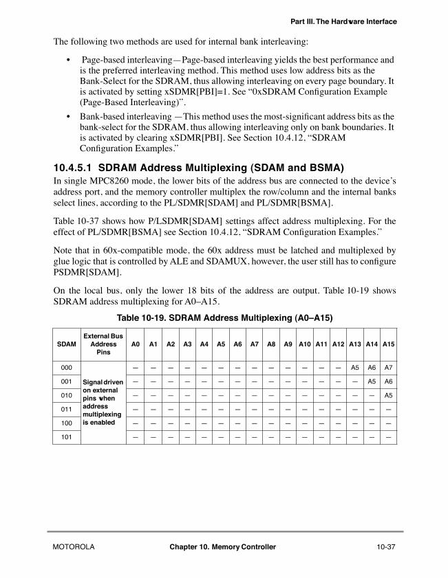
Part III. The Hardware Interface
The following two methods are used for internal bank interleaving:
¥ Page-based interleavingÑPage-based interleaving yields the best performance and is the preferred interleaving method. This method uses low address bits as the Bank-Select for the SDRAM, thus allowing interleaving on every page boundary. It is activated by setting xSDMR[PBI]=1. See Ò0xSDRAM ConÞguration Example (Page-Based Interleaving)Ó.
¥ Bank-based interleaving ÑThis method uses the most-signiÞcant address bits as the bank-select for the SDRAM, thus allowing interleaving only on bank boundaries. It is activated by clearing xSDMR[PBI]. See Section 10.4.12, ÒSDRAM ConÞguration Examples.Ó
10.4.5.1 SDRAM Address Multiplexing (SDAM and BSMA)In single MPC8260 mode, the lower bits of the address bus are connected to the deviceÕsaddress port, and the memory controller multiplex the row/column and the internal banksselect lines, according to the PL/SDMR[SDAM] and PL/SDMR[BSMA].
Table 10-37 shows how P/LSDMR[SDAM] settings affect address multiplexing. For theeffect of PL/SDMR[BSMA] see Section 10.4.12, ÒSDRAM ConÞguration Examples.Ó
Note that in 60x-compatible mode, the 60x address must be latched and multiplexed byglue logic that is controlled by ALE and SDAMUX, however, the user still has to conÞgurePSDMR[SDAM].
On the local bus, only the lower 18 bits of the address are output. Table 10-19 showsSDRAM address multiplexing for A0ÐA15.
Table 10-19. SDRAM Address Multiplexing (A0ÐA15)
SDAMExternal Bus
Address Pins
A0 A1 A2 A3 A4 A5 A6 A7 A8 A9 A10 A11 A12 A13 A14 A15
000
Signal driven on external pins when address multiplexing is enabled
Ñ Ñ Ñ Ñ Ñ Ñ Ñ Ñ Ñ Ñ Ñ Ñ Ñ A5 A6 A7
001 Ñ Ñ Ñ Ñ Ñ Ñ Ñ Ñ Ñ Ñ Ñ Ñ Ñ Ñ A5 A6
010 Ñ Ñ Ñ Ñ Ñ Ñ Ñ Ñ Ñ Ñ Ñ Ñ Ñ Ñ Ñ A5
011 Ñ Ñ Ñ Ñ Ñ Ñ Ñ Ñ Ñ Ñ Ñ Ñ Ñ Ñ Ñ Ñ
100 Ñ Ñ Ñ Ñ Ñ Ñ Ñ Ñ Ñ Ñ Ñ Ñ Ñ Ñ Ñ Ñ
101 Ñ Ñ Ñ Ñ Ñ Ñ Ñ Ñ Ñ Ñ Ñ Ñ Ñ Ñ Ñ Ñ
MOTOROLA Chapter 10. Memory Controller 10-37
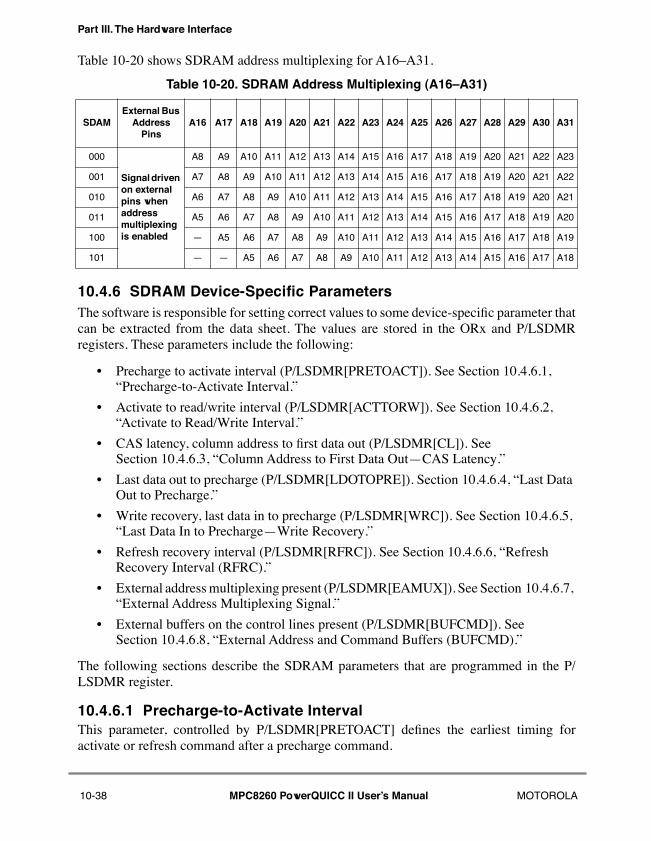
Part III. The Hardware Interface
Table 10-20 shows SDRAM address multiplexing for A16ÐA31.
10.4.6 SDRAM Device-SpeciÞc ParametersThe software is responsible for setting correct values to some device-speciÞc parameter thatcan be extracted from the data sheet. The values are stored in the ORx and P/LSDMRregisters. These parameters include the following:
¥ Precharge to activate interval (P/LSDMR[PRETOACT]). See Section 10.4.6.1, ÒPrecharge-to-Activate Interval.Ó
¥ Activate to read/write interval (P/LSDMR[ACTTORW]). See Section 10.4.6.2, ÒActivate to Read/Write Interval.Ó
¥ CAS latency, column address to Þrst data out (P/LSDMR[CL]). See Section 10.4.6.3, ÒColumn Address to First Data OutÑCAS Latency.Ó
¥ Last data out to precharge (P/LSDMR[LDOTOPRE]). Section 10.4.6.4, ÒLast Data Out to Precharge.Ó
¥ Write recovery, last data in to precharge (P/LSDMR[WRC]). See Section 10.4.6.5, ÒLast Data In to PrechargeÑWrite Recovery.Ó
¥ Refresh recovery interval (P/LSDMR[RFRC]). See Section 10.4.6.6, ÒRefresh Recovery Interval (RFRC).Ó
¥ External address multiplexing present (P/LSDMR[EAMUX]). See Section 10.4.6.7, ÒExternal Address Multiplexing Signal.Ó
¥ External buffers on the control lines present (P/LSDMR[BUFCMD]). See Section 10.4.6.8, ÒExternal Address and Command Buffers (BUFCMD).Ó
The following sections describe the SDRAM parameters that are programmed in the P/LSDMR register.
10.4.6.1 Precharge-to-Activate Interval This parameter, controlled by P/LSDMR[PRETOACT] deÞnes the earliest timing foractivate or refresh command after a precharge command.
Table 10-20. SDRAM Address Multiplexing (A16ÐA31)
SDAMExternal Bus
Address Pins
A16 A17 A18 A19 A20 A21 A22 A23 A24 A25 A26 A27 A28 A29 A30 A31
000
Signal driven on external pins when address multiplexing is enabled
A8 A9 A10 A11 A12 A13 A14 A15 A16 A17 A18 A19 A20 A21 A22 A23
001 A7 A8 A9 A10 A11 A12 A13 A14 A15 A16 A17 A18 A19 A20 A21 A22
010 A6 A7 A8 A9 A10 A11 A12 A13 A14 A15 A16 A17 A18 A19 A20 A21
011 A5 A6 A7 A8 A9 A10 A11 A12 A13 A14 A15 A16 A17 A18 A19 A20
100 Ñ A5 A6 A7 A8 A9 A10 A11 A12 A13 A14 A15 A16 A17 A18 A19
101 Ñ Ñ A5 A6 A7 A8 A9 A10 A11 A12 A13 A14 A15 A16 A17 A18
10-38 MPC8260 PowerQUICC II UserÕs Manual MOTOROLA
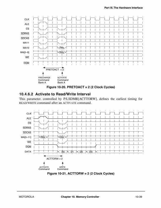
Part III. The Hardware Interface
Figure 10-20. PRETOACT = 2 (2 Clock Cycles)
10.4.6.2 Activate to Read/Write Interval This parameter, controlled by P/LSDMR[ACTTORW], deÞnes the earliest timing forREAD/WRITE command after an ACTIVATE command.
Figure 10-21. ACTTORW = 2 (2 Clock Cycles)
CLK
ALE
CS
SDRAS
SDCAS
WE
DQM
PRECHARGE Command
ACTIVATE
MA11
MA10
MA[0Ð9] RAy
RAy
Bank ACommand Bank A
PRETOACT = 2
CLK
ALE
CS
SDRAS
SDCAS
Rbz
WE
DQM
ACTIVATE
MA[0Ð11]
Command
ACTTORW = 2
DATA D0 D1 D2 D3
WRITE Command
Cbz
MOTOROLA Chapter 10. Memory Controller 10-39
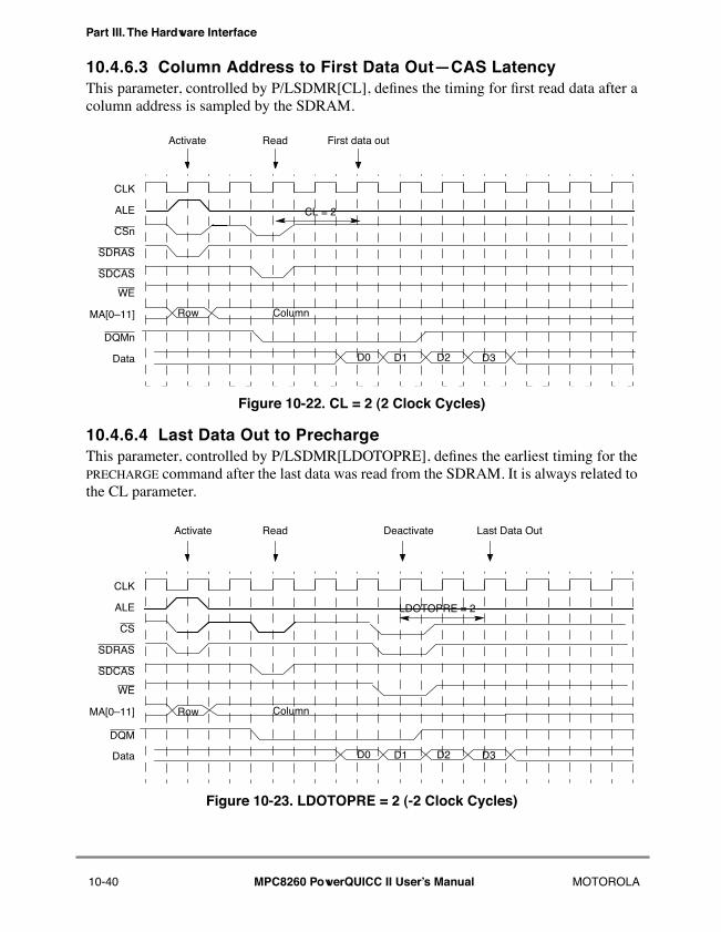
Part III. The Hardware Interface
10.4.6.3 Column Address to First Data OutÑCAS Latency This parameter, controlled by P/LSDMR[CL], deÞnes the timing for Þrst read data after acolumn address is sampled by the SDRAM.
Figure 10-22. CL = 2 (2 Clock Cycles)
10.4.6.4 Last Data Out to Precharge This parameter, controlled by P/LSDMR[LDOTOPRE], deÞnes the earliest timing for thePRECHARGE command after the last data was read from the SDRAM. It is always related tothe CL parameter.
Figure 10-23. LDOTOPRE = 2 (-2 Clock Cycles)
CLK
ALE
CSn
SDRAS
SDCAS
MA[0Ð11] Row Column
WE
DQMn
Data D0 D1 D2 D3
Activate Read First data out
CL = 2
CLK
ALE
CS
SDRAS
SDCAS
MA[0Ð11] Row Column
WE
Data D0 D1 D2 D3
Activate Read Deactivate Last Data Out
LDOTOPRE = 2
DQM
10-40 MPC8260 PowerQUICC II UserÕs Manual MOTOROLA
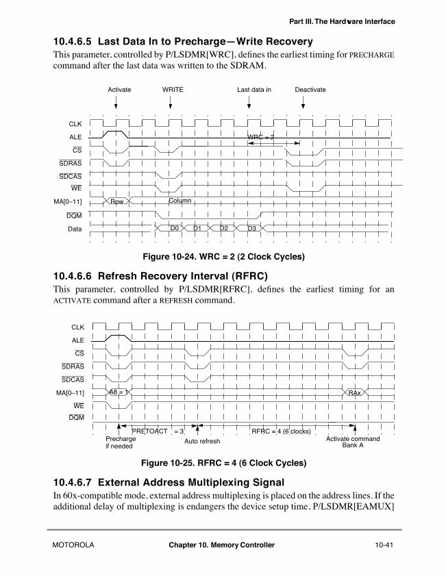
Part III. The Hardware Interface
10.4.6.5 Last Data In to PrechargeÑWrite Recovery This parameter, controlled by P/LSDMR[WRC], deÞnes the earliest timing for PRECHARGE
command after the last data was written to the SDRAM.
Figure 10-24. WRC = 2 (2 Clock Cycles)
10.4.6.6 Refresh Recovery Interval (RFRC)This parameter, controlled by P/LSDMR[RFRC], deÞnes the earliest timing for anACTIVATE command after a REFRESH command.
Figure 10-25. RFRC = 4 (6 Clock Cycles)
10.4.6.7 External Address Multiplexing Signal In 60x-compatible mode, external address multiplexing is placed on the address lines. If theadditional delay of multiplexing is endangers the device setup time, P/LSDMR[EAMUX]
CLK
ALE
CS
SDRAS
SDCAS
MA[0Ð11] Row Column
WE
Data D0 D1 D2 D3
Activate WRITE Last data in Deactivate
WRC = 2
DQM
CLK
ALE
CS
SDRAS
SDCAS
MA[0Ð11]
WE
DQM
A8 = 1
RFRC = 4 (6 clocks)
RAx
PRETOACT = 3Precharge if needed
Auto refresh Activate commandBank A
MOTOROLA Chapter 10. Memory Controller 10-41
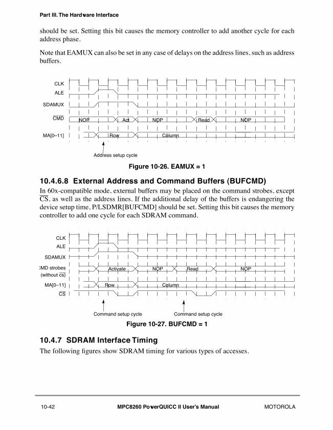
Part III. The Hardware Interface
should be set. Setting this bit causes the memory controller to add another cycle for eachaddress phase.
Note that EAMUX can also be set in any case of delays on the address lines, such as addressbuffers.
Figure 10-26. EAMUX = 1
10.4.6.8 External Address and Command Buffers (BUFCMD)In 60x-compatible mode, external buffers may be placed on the command strobes, exceptCS, as well as the address lines. If the additional delay of the buffers is endangering thedevice setup time, P/LSDMR[BUFCMD] should be set. Setting this bit causes the memorycontroller to add one cycle for each SDRAM command.
Figure 10-27. BUFCMD = 1
10.4.7 SDRAM Interface TimingThe following Þgures show SDRAM timing for various types of accesses.
CLK
SDAMUX
CMD
MA[0Ð11] Row Column
NOP Act Read NOPNOP
Address setup cycle
ALE
CLK
SDAMUX
CMD strobes
MA[0Ð11] Row Column
Activate Read NOPNOP(without cs)
CS
ALE
Command setup cycle Command setup cycle
10-42 MPC8260 PowerQUICC II UserÕs Manual MOTOROLA
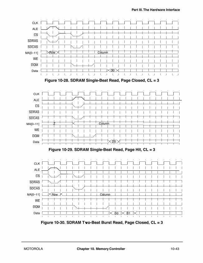
Part III. The Hardware Interface
Figure 10-28. SDRAM Single-Beat Read, Page Closed, CL = 3
Figure 10-29. SDRAM Single-Beat Read, Page Hit, CL = 3
Figure 10-30. SDRAM Two-Beat Burst Read, Page Closed, CL = 3
CLK
ALE
CS
SDRAS
SDCAS
MA[0Ð11] Row Column
WE
DQM
Data D0
CLK
ALE
CS
SDRAS
SDCAS
MA[0Ð11] Column
WE
DQM
Data D0
Z
CLK
ALE
CS
SDRAS
SDCAS
MA[0Ð11] Row Column
WE
DQM
Data D0 D1
MOTOROLA Chapter 10. Memory Controller 10-43
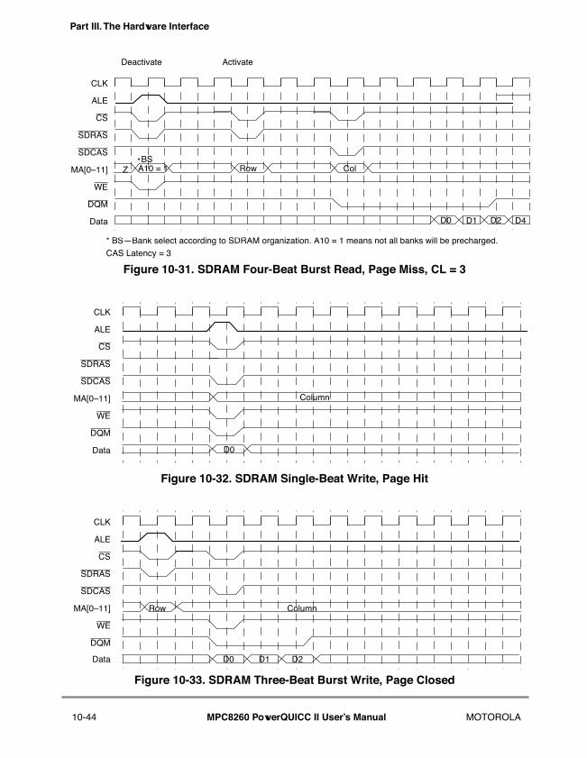
Part III. The Hardware Interface
Figure 10-31. SDRAM Four-Beat Burst Read, Page Miss, CL = 3
Figure 10-32. SDRAM Single-Beat Write, Page Hit
Figure 10-33. SDRAM Three-Beat Burst Write, Page Closed
CLK
ALE
CS
SDRAS
SDCAS
MA[0Ð11]
WE
DQM
Data D0
Z A10 = 1BS*
* BSÑBank select according to SDRAM organization. A10 = 1 means not all banks will be precharged.
Row
CAS Latency = 3
Col
D1 D2 D4
Deactivate Activate
CLK
ALE
CS
SDRAS
SDCAS
MA[0Ð11] Column
WE
DQM
Data D0
CLK
ALE
CS
SDRAS
SDCAS
MA[0Ð11] Row Column
WE
DQM
Data D0 D1 D2
10-44 MPC8260 PowerQUICC II UserÕs Manual MOTOROLA
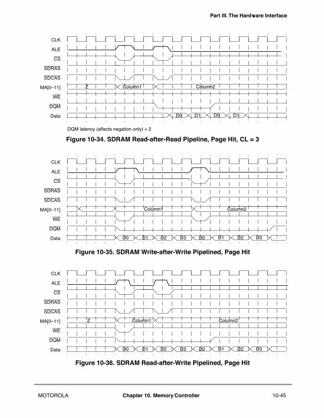
Part III. The Hardware Interface
Figure 10-34. SDRAM Read-after-Read Pipeline, Page Hit, CL = 3
Figure 10-35. SDRAM Write-after-Write Pipelined, Page Hit
Figure 10-36. SDRAM Read-after-Write Pipelined, Page Hit
CLK
ALE
CS
SDRAS
SDCAS
MA[0Ð11] Column1
WE
DQM
Data D0
Z Column2
D0 D1D1
DQM latency (affects negation only) = 2
CLK
ALE
CS
SDRAS
SDCAS
MA[0Ð11] Column1
WE
DQM
Data D0 D1 D2 D3 D1 D2 D3D0
Column2
CLK
ALE
CS
SDRAS
SDCAS
MA[0Ð11] Column1
WE
DQM
Data D0 D1 D2 D3 D1 D2 D3D0
Column2Z
MOTOROLA Chapter 10. Memory Controller 10-45
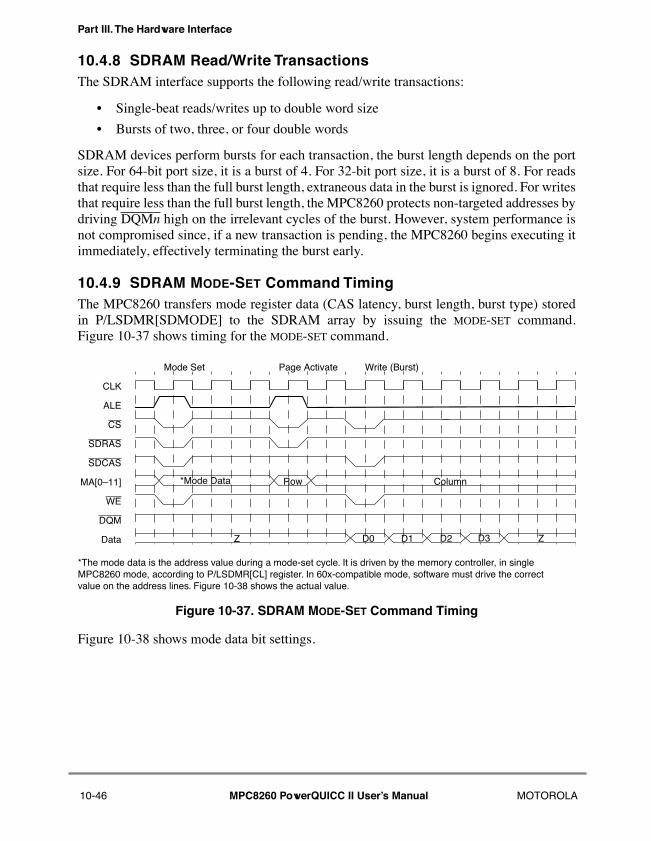
Part III. The Hardware Interface
10.4.8 SDRAM Read/Write TransactionsThe SDRAM interface supports the following read/write transactions:
¥ Single-beat reads/writes up to double word size
¥ Bursts of two, three, or four double words
SDRAM devices perform bursts for each transaction, the burst length depends on the portsize. For 64-bit port size, it is a burst of 4. For 32-bit port size, it is a burst of 8. For readsthat require less than the full burst length, extraneous data in the burst is ignored. For writesthat require less than the full burst length, the MPC8260 protects non-targeted addresses bydriving DQMn high on the irrelevant cycles of the burst. However, system performance isnot compromised since, if a new transaction is pending, the MPC8260 begins executing itimmediately, effectively terminating the burst early.
10.4.9 SDRAM MODE-SET Command TimingThe MPC8260 transfers mode register data (CAS latency, burst length, burst type) storedin P/LSDMR[SDMODE] to the SDRAM array by issuing the MODE-SET command.Figure 10-37 shows timing for the MODE-SET command.
Figure 10-37. SDRAM MODE-SET Command Timing
Figure 10-38 shows mode data bit settings.
CLK
ALE
CS
SDRAS
SDCAS
MA[0Ð11]
WE
DQM
Data Z ZD0 D1 D2 D3
*Mode Data Row Column
*The mode data is the address value during a mode-set cycle. It is driven by the memory controller, in single MPC8260 mode, according to P/LSDMR[CL] register. In 60x-compatible mode, software must drive the correct value on the address lines. Figure 10-38 shows the actual value.
Mode Set Page Activate Write (Burst)
10-46 MPC8260 PowerQUICC II UserÕs Manual MOTOROLA
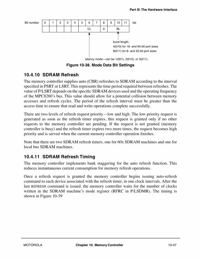
Part III. The Hardware Interface
Figure 10-38. Mode Data Bit Settings
10.4.10 SDRAM RefreshThe memory controller supplies auto (CBR) refreshes to SDRAM according to the intervalspeciÞed in PSRT or LSRT. This represents the time period required between refreshes. Thevalue of P/LSRT depends on the speciÞc SDRAM devices used and the operating frequencyof the MPC8260Õs bus. This value should allow for a potential collision between memoryaccesses and refresh cycles. The period of the refresh interval must be greater than theaccess time to ensure that read and write operations complete successfully.
There are two levels of refresh request priorityÑlow and high. The low priority request isgenerated as soon as the refresh timer expires, this request is granted only if no otherrequests to the memory controller are pending. If the request is not granted (memorycontroller is busy) and the refresh timer expires two more times, the request becomes highpriority and is served when the current memory controller operation Þnishes.
Note that there are two SDRAM refresh timers, one for 60x SDRAM machines and one forlocal bus SDRAM machines.
10.4.11 SDRAM Refresh TimingThe memory controller implements bank staggering for the auto refresh function. Thisreduces instantaneous current consumption for memory refresh operations.
Once a refresh request is granted the memory controller begins issuing auto-refreshcommand to each device associated with the refresh timer, in one clock intervals. After thelast REFRESH command is issued, the memory controller waits for the number of clockswritten in the SDRAM machineÕs mode register (RFRC in P/LSDMR). The timing isshown in Figure 10-39
latency modeÑcan be 1(001), 2(010), or 3(011).
burst length:
4(010) for 16- and 64-bit port sizes
8(011) for 8- and 32-bit port sizes
Bit number 0 1 2 3 4 5 6 7 8 9 10 11 lsb
CL 0 BL
MOTOROLA Chapter 10. Memory Controller 10-47
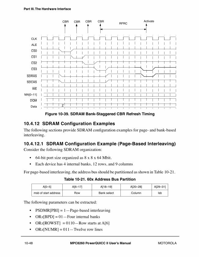
Part III. The Hardware Interface
Figure 10-39. SDRAM Bank-Staggered CBR Refresh Timing
10.4.12 SDRAM ConÞguration ExamplesThe following sections provide SDRAM conÞguration examples for page- and bank-basedinterleaving.
10.4.12.1 SDRAM ConÞguration Example (Page-Based Interleaving)Consider the following SDRAM organization:
¥ 64-bit port size organized as 8 x 8 x 64 Mbit.
¥ Each device has 4 internal banks, 12 rows, and 9 columns
For page-based interleaving, the address bus should be partitioned as shown in Table 10-21.
The following parameters can be extracted:
¥ PSDMR[PBI] = 1ÑPage-based interleaving
¥ ORx[BPD] = 01ÑFour internal banks
¥ ORx[ROWST] = 0110ÑRow starts at A[6]
¥ ORx[NUMR] = 011ÑTwelve row lines
Table 10-21. 60x Address Bus Partition
A[0Ð5] A[6Ð17] A[18Ð19] A[20Ð28] A[29Ð31]
msb of start address Row Bank select Column lsb
CLK
ALE
CS0
SDRAS
SDCAS
MA[0Ð11]
WE
DQM
Data
CS1
CS2
CS3
RFRCCBR CBR CBR CBR Activate
Z
10-48 MPC8260 PowerQUICC II UserÕs Manual MOTOROLA
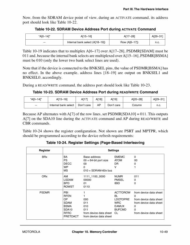
Part III. The Hardware Interface
Now, from the SDRAM device point of view, during an ACTIVATE command, its addressport should look like Table 10-22.
Table 10-19 indicates that to multiplex A[6Ð17] over A[17Ð28], PSDMR[SDAM] must be011 and, because the internal bank selects are multiplexed over A[15Ð16], PSDMR[BSMA]must be 010 (only the lower two bank select lines are used).
Note that if the device is connected to the BNKSEL pins, the value of PSDMR[BSMA] hasno effect. In the above example, address lines [18Ð19] are output on BNKSEL1 andBNKSEL0, accordingly.
During a READ/WRITE command, the address port should look like Table 10-23.
Because AP alternates with A[7] of the row lines, set PSDMR[SDA10] = 011. This outputsA[7] on the SDA10 line during the ACTIVATE command and AP during READ/WRITE andCBR commands.
Table 10-24 shows the register conÞguration. Not shown are PSRT and MPTPR, whichshould be programmed according to the device refresh requirements:
Table 10-22. SDRAM Device Address Port during ACTIVATE Command
ÒA[0Ð14]Ó A[15Ð16] A[17Ð28] A[29Ð31]
Ñ Internal bank select (A[18Ð19]) Row (A[6Ð17]) n.c.
Table 10-23. SDRAM Device Address Port during READ/WRITE Command
ÒA[0Ð14]Ó A[15Ð16] A[17] A[18] A[19] A[20Ð28] A[29Ð31]
Ñ Internal bank select DonÕt care AP DonÕt care Column n.c.
Table 10-24. Register Settings (Page-Based Interleaving
Register Settings
BRx BA Base address PS 00 = 64-bit port sizeDECC 00WP 0MS 010 = SDRAM-60x bus
EMEMC 0ATOM 00DR 0V 1
ORx AM 1111_1100_0000LSDAM 00000BPD 01ROWST 0110
NUMR 011PMSEL 0IBID 0
PSDMR PBI 1RFEN 1OP 000SDAM 011BSMA 010SDA10 011RFRC from device data sheetPRETOACT from device data sheet
ACTTOROW from device data sheetBL 0LDOTOPRE from device data sheetWRC from device data sheetEAMUX 0BUFCMD 0CL from device data sheet
MOTOROLA Chapter 10. Memory Controller 10-49
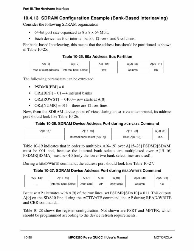
Part III. The Hardware Interface
10.4.13 SDRAM ConÞguration Example (Bank-Based Interleaving)Consider the following SDRAM organization:
¥ 64-bit port size organized as 8 x 8 x 64 Mbit.
¥ Each device has four internal banks, 12 rows, and 9 columns
For bank-based Interleaving, this means that the address bus should be partitioned as shownin Table 10-25.
The following parameters can be extracted:
¥ PSDMR[PBI] = 0
¥ ORx[BPD] = 01Ñ4 internal banks
¥ ORx[ROWST] = 0100Ñrow starts at A[8]
¥ ORx[NUMR] = 011Ñthere are 12 row lines
Now, from the SDRAM device point of view, during an ACTIVATE command, its addressport should look like Table 10-26.
Table 10-19 indicates that in order to multiplex A[6Ð19] over A[15Ð28] PSDMR[SDAM]must be 001 and, because the internal bank selects are multiplexed over A[15Ð16]PSDMR[BSMA] must be 010 (only the lower two bank select lines are used).
During a READ/WRITE command, the address port should look like Table 10-27.
Because AP alternates with A[9] of the row lines, set PSDMR[SDA10] = 011. This outputsA[9] on the SDA10 line during the ACTIVATE command and AP during READ/WRITEand CBR commands.
Table 10-28 shows the register conÞguration. Not shown are PSRT and MPTPR, whichshould be programmed according to the device refresh requirements.
Table 10-25. 60x Address Bus Partition
A[0Ð5] A[6Ð7] A[8Ð19] A[20Ð28] A[29Ð31]
msb of start address Internal bank select Row Column lsb
Table 10-26. SDRAM Device Address Port during ACTIVATE Command
ÒA[0Ð14]Ó A[15Ð16] A[17Ð28] A[29Ð31]
Ñ Internal bank select (A[6Ð7]) Row (A[8Ð19]) n.c.
Table 10-27. SDRAM Device Address Port during READ/WRITE Command
ÒA[0Ð14]Ó A[15Ð16] A[17] A[18] A[19] A[20Ð28] A[29Ð31]
Ñ Internal bank select DonÕt care AP DonÕt care Column n.c.
10-50 MPC8260 PowerQUICC II UserÕs Manual MOTOROLA
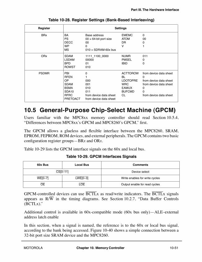
Part III. The Hardware Interface
10.5 General-Purpose Chip-Select Machine (GPCM)Users familiar with the MPC8xx memory controller should read Section 10.5.4,ÒDifferences between MPC8xxÕs GPCM and MPC8260Õs GPCM,Ó Þrst.
The GPCM allows a glueless and ßexible interface between the MPC8260, SRAM,EPROM, FEPROM, ROM devices, and external peripherals. The GPCM contains two basicconÞguration register groupsÑBRx and ORx.
Table 10-29 lists the GPCM interface signals on the 60x and local bus.
GPCM-controlled devices can use BCTLx as read/write indicators. The BCTLx signalsappears as R/W in the timing diagrams. See Section 10.2.7, ÒData Buffer Controls(BCTLx).Ó
Additional control is available in 60x-compatible mode (60x bus only)ÑALEÐexternaladdress latch enable
In this section, when a signal is named, the reference is to the 60x or local bus signal,according to the bank being accessed. Figure 10-40 shows a simple connection between a32-bit port size SRAM device and the MPC8260.
Table 10-28. Register Settings (Bank-Based Interleaving)
Register Settings
BRx BA Base address PS 00 = 64-bit port sizeDECC 00WP 0MS 010 = SDRAM-60x bus
EMEMC 0ATOM 00DR 0V 1
ORx SDAM 1111_1100_0000LSDAM 00000BPD 01ROWST 010
NUMR 011PMSEL 0IBID 0
PSDMR PBI 0RFEN 1OP 000SDAM 001BSMA 010SDA10 011RFRC from device data sheetPRETOACT from device data sheet
ACTTOROW from device data sheetBL 0LDOTOPRE from device data sheetWRC from device data sheetEAMUX 0BUFCMD 0CL from device data sheet
Table 10-29. GPCM Interfaces Signals
60x Bus Local Bus Comments
CS[0Ð11] Device select
WE[0Ð7] LWE[0Ð3] Write enables for write cycles
OE LOE Output enable for read cycles
MOTOROLA Chapter 10. Memory Controller 10-51
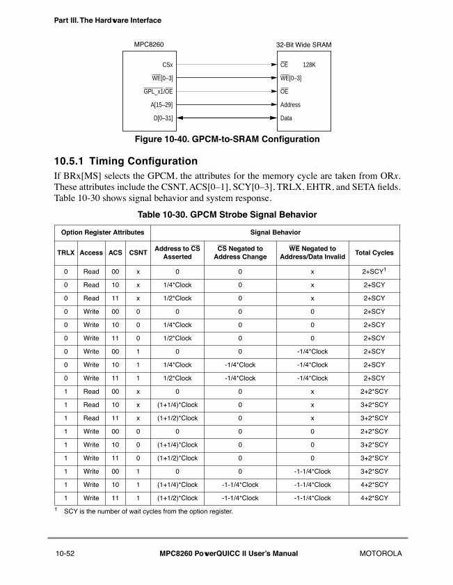
Part III. The Hardware Interface
Figure 10-40. GPCM-to-SRAM ConÞguration
10.5.1 Timing ConÞgurationIf BRx[MS] selects the GPCM, the attributes for the memory cycle are taken from ORx.These attributes include the CSNT, ACS[0Ð1], SCY[0Ð3], TRLX, EHTR, and SETA Þelds.Table 10-30 shows signal behavior and system response.
Table 10-30. GPCM Strobe Signal Behavior
Option Register Attributes Signal Behavior
TRLX Access ACS CSNT Address to CS
AssertedCS Negated to
Address Change WE Negated to
Address/Data InvalidTotal Cycles
0 Read 00 x 0 0 x 2+SCY1
1 SCY is the number of wait cycles from the option register.
0 Read 10 x 1/4*Clock 0 x 2+SCY
0 Read 11 x 1/2*Clock 0 x 2+SCY
0 Write 00 0 0 0 0 2+SCY
0 Write 10 0 1/4*Clock 0 0 2+SCY
0 Write 11 0 1/2*Clock 0 0 2+SCY
0 Write 00 1 0 0 -1/4*Clock 2+SCY
0 Write 10 1 1/4*Clock -1/4*Clock -1/4*Clock 2+SCY
0 Write 11 1 1/2*Clock -1/4*Clock -1/4*Clock 2+SCY
1 Read 00 x 0 0 x 2+2*SCY
1 Read 10 x (1+1/4)*Clock 0 x 3+2*SCY
1 Read 11 x (1+1/2)*Clock 0 x 3+2*SCY
1 Write 00 0 0 0 0 2+2*SCY
1 Write 10 0 (1+1/4)*Clock 0 0 3+2*SCY
1 Write 11 0 (1+1/2)*Clock 0 0 3+2*SCY
1 Write 00 1 0 0 -1-1/4*Clock 3+2*SCY
1 Write 10 1 (1+1/4)*Clock -1-1/4*Clock -1-1/4*Clock 4+2*SCY
1 Write 11 1 (1+1/2)*Clock -1-1/4*Clock -1-1/4*Clock 4+2*SCY
CE
WE[0–3]
OE
Address
Data
32-Bit Wide SRAM
D[0–31]
A[15–29]
GPL_x1/OE
WE[0–3]
CSx
128K
MPC8260
10-52 MPC8260 PowerQUICC II UserÕs Manual MOTOROLA
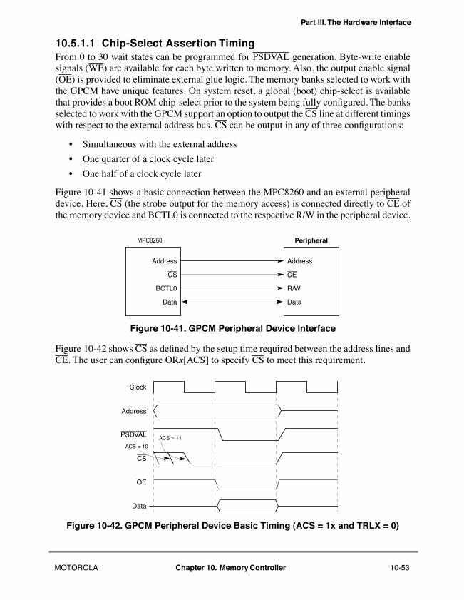
Part III. The Hardware Interface
10.5.1.1 Chip-Select Assertion Timing From 0 to 30 wait states can be programmed for PSDVAL generation. Byte-write enablesignals (WE) are available for each byte written to memory. Also, the output enable signal(OE) is provided to eliminate external glue logic. The memory banks selected to work withthe GPCM have unique features. On system reset, a global (boot) chip-select is availablethat provides a boot ROM chip-select prior to the system being fully conÞgured. The banksselected to work with the GPCM support an option to output the CS line at different timingswith respect to the external address bus. CS can be output in any of three conÞgurations:
¥ Simultaneous with the external address
¥ One quarter of a clock cycle later
¥ One half of a clock cycle later
Figure 10-41 shows a basic connection between the MPC8260 and an external peripheraldevice. Here, CS (the strobe output for the memory access) is connected directly to CE ofthe memory device and BCTL0 is connected to the respective R/W in the peripheral device.
Figure 10-41. GPCM Peripheral Device Interface
Figure 10-42 shows CS as deÞned by the setup time required between the address lines andCE. The user can conÞgure ORx[ACS] to specify CS to meet this requirement.
Figure 10-42. GPCM Peripheral Device Basic Timing (ACS = 1x and TRLX = 0)
Address
CE
R/W
Data
Peripheral
Data
BCTL0
CS
Address
MPC8260
Clock
Address
PSDVAL
CS
OE
Data
ACS = 11
ACS = 10
MOTOROLA Chapter 10. Memory Controller 10-53
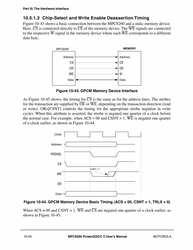
Part III. The Hardware Interface
10.5.1.2 Chip-Select and Write Enable Deassertion Timing Figure 10-43 shows a basic connection between the MPC8260 and a static memory device.Here, CS is connected directly to CE of the memory device. The WE signals are connectedto the respective W signal in the memory device where each WE corresponds to a differentdata byte.
Figure 10-43. GPCM Memory Device Interface
As Figure 10-45 shows, the timing for CS is the same as for the address lines. The strobesfor the transaction are supplied by OE or WE, depending on the transaction direction (reador write). ORx[CSNT] controls the timing for the appropriate strobe negation in writecycles. When this attribute is asserted, the strobe is negated one quarter of a clock beforethe normal case. For example, when ACS = 00 and CSNT = 1, WE is negated one quarterof a clock earlier, as shown in Figure 10-44.
Figure 10-44. GPCM Memory Device Basic Timing (ACS = 00, CSNT = 1, TRLX = 0)
When ACS ¹ 00 and CSNT = 1, WE and CS are negated one quarter of a clock earlier, asshown in Figure 10-45.
Address
CE
OE
W
Data
MEMORY
Data
WE
OE
CS
Address
MPC8260
Clock
Address
PSDVAL
CS
WE
OE
Data
CSNT = 1
10-54 MPC8260 PowerQUICC II UserÕs Manual MOTOROLA
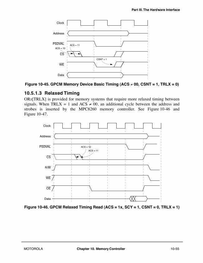
Part III. The Hardware Interface
Figure 10-45. GPCM Memory Device Basic Timing (ACS ¹ 00, CSNT = 1, TRLX = 0)
10.5.1.3 Relaxed TimingORx[TRLX] is provided for memory systems that require more relaxed timing betweensignals. When TRLX = 1 and ACS ¹ 00, an additional cycle between the address andstrobes is inserted by the MPC8260 memory controller. See Figure 10-46 andFigure 10-47.
Figure 10-46. GPCM Relaxed Timing Read (ACS = 1x, SCY = 1, CSNT = 0, TRLX = 1)
Clock
Address
PSDVAL
CS
WE
Data
CSNT = 1
ACS = 11ACS = 10
Clock
Address
PSDVAL
CS
R/W
WE
OE
Data
ACS = 10
ACS = 11
MOTOROLA Chapter 10. Memory Controller 10-55
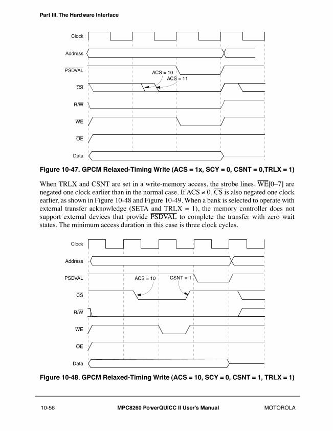
Part III. The Hardware Interface
Figure 10-47. GPCM Relaxed-Timing Write (ACS = 1x, SCY = 0, CSNT = 0,TRLX = 1)
When TRLX and CSNT are set in a write-memory access, the strobe lines, WE[0Ð7] arenegated one clock earlier than in the normal case. If ACS ¹ 0, CS is also negated one clockearlier, as shown in Figure 10-48 and Figure 10-49. When a bank is selected to operate withexternal transfer acknowledge (SETA and TRLX = 1), the memory controller does notsupport external devices that provide PSDVAL to complete the transfer with zero waitstates. The minimum access duration in this case is three clock cycles.
Figure 10-48. GPCM Relaxed-Timing Write (ACS = 10, SCY = 0, CSNT = 1, TRLX = 1)
Clock
Address
PSDVAL
CS
R/W
WE
OE
Data
ACS = 10ACS = 11
Clock
Address
PSDVAL
CS
R/W
WE
OE
Data
ACS = 10 CSNT = 1
10-56 MPC8260 PowerQUICC II UserÕs Manual MOTOROLA
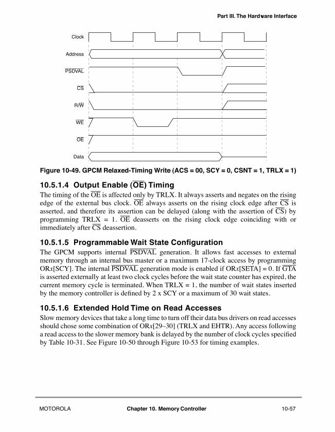
Part III. The Hardware Interface
Figure 10-49. GPCM Relaxed-Timing Write (ACS = 00, SCY = 0, CSNT = 1, TRLX = 1)
10.5.1.4 Output Enable (OE) Timing The timing of the OE is affected only by TRLX. It always asserts and negates on the risingedge of the external bus clock. OE always asserts on the rising clock edge after CS isasserted, and therefore its assertion can be delayed (along with the assertion of CS) byprogramming TRLX = 1. OE deasserts on the rising clock edge coinciding with orimmediately after CS deassertion.
10.5.1.5 Programmable Wait State ConÞgurationThe GPCM supports internal PSDVAL generation. It allows fast accesses to externalmemory through an internal bus master or a maximum 17-clock access by programmingORx[SCY]. The internal PSDVAL generation mode is enabled if ORx[SETA] = 0. If GTAis asserted externally at least two clock cycles before the wait state counter has expired, thecurrent memory cycle is terminated. When TRLX = 1, the number of wait states insertedby the memory controller is deÞned by 2 x SCY or a maximum of 30 wait states.
10.5.1.6 Extended Hold Time on Read AccessesSlow memory devices that take a long time to turn off their data bus drivers on read accessesshould chose some combination of ORx[29Ð30] (TRLX and EHTR). Any access followinga read access to the slower memory bank is delayed by the number of clock cycles speciÞedby Table 10-31. See Figure 10-50 through Figure 10-53 for timing examples.
Clock
Address
PSDVAL
CS
R/W
WE
OE
Data
MOTOROLA Chapter 10. Memory Controller 10-57
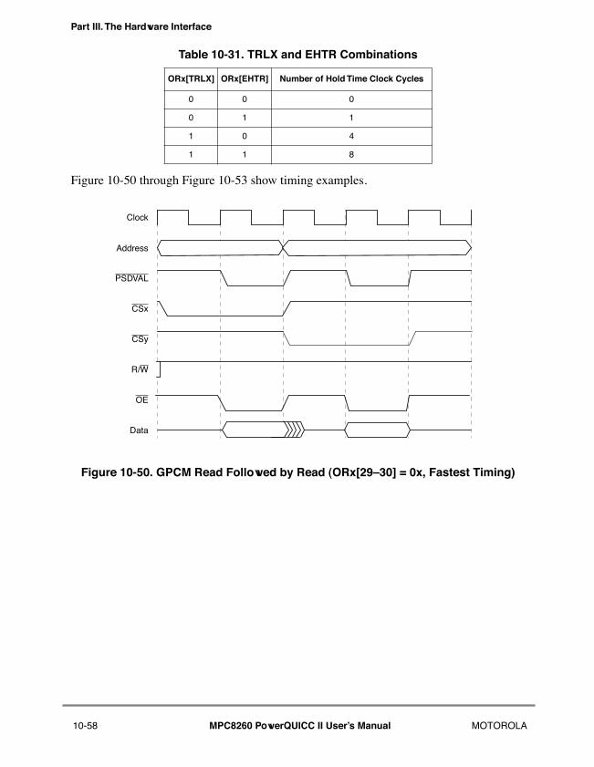
Part III. The Hardware Interface
Figure 10-50 through Figure 10-53 show timing examples.
Figure 10-50. GPCM Read Followed by Read (ORx[29Ð30] = 0x, Fastest Timing)
Table 10-31. TRLX and EHTR Combinations
ORx[TRLX] ORx[EHTR] Number of Hold Time Clock Cycles
0 0 0
0 1 1
1 0 4
1 1 8
Clock
Address
PSDVAL
CSx
CSy
R/W
OE
Data
10-58 MPC8260 PowerQUICC II UserÕs Manual MOTOROLA
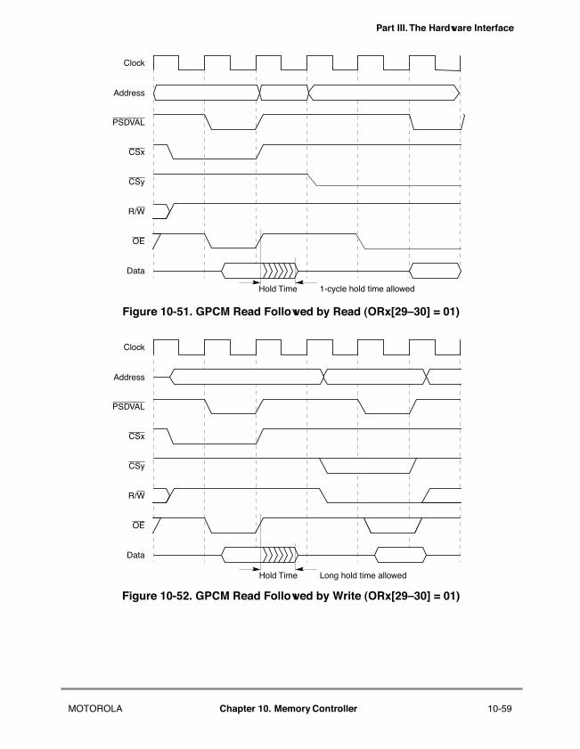
Part III. The Hardware Interface
Figure 10-51. GPCM Read Followed by Read (ORx[29Ð30] = 01)
Figure 10-52. GPCM Read Followed by Write (ORx[29Ð30] = 01)
Clock
Address
PSDVAL
CSx
CSy
R/W
OE
Data
Hold Time 1-cycle hold time allowed
Clock
Address
PSDVAL
CSx
CSy
R/W
OE
Data
Hold Time Long hold time allowed
MOTOROLA Chapter 10. Memory Controller 10-59
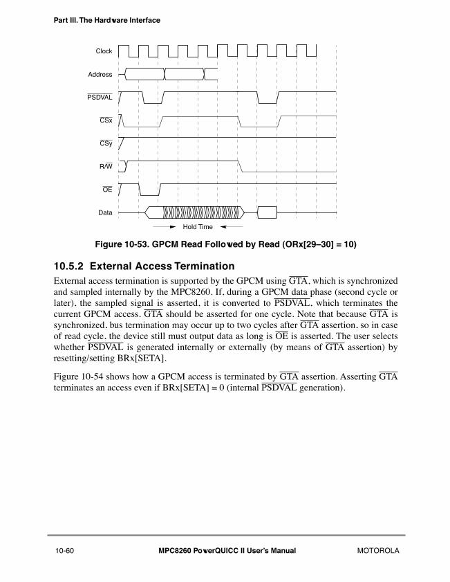
Part III. The Hardware Interface
Figure 10-53. GPCM Read Followed by Read (ORx[29Ð30] = 10)
10.5.2 External Access TerminationExternal access termination is supported by the GPCM using GTA, which is synchronizedand sampled internally by the MPC8260. If, during a GPCM data phase (second cycle orlater), the sampled signal is asserted, it is converted to PSDVAL, which terminates thecurrent GPCM access. GTA should be asserted for one cycle. Note that because GTA issynchronized, bus termination may occur up to two cycles after GTA assertion, so in caseof read cycle, the device still must output data as long is OE is asserted. The user selectswhether PSDVAL is generated internally or externally (by means of GTA assertion) byresetting/setting BRx[SETA].
Figure 10-54 shows how a GPCM access is terminated by GTA assertion. Asserting GTAterminates an access even if BRx[SETA] = 0 (internal PSDVAL generation).
Clock
Address
PSDVAL
CSx
CSy
R/W
OE
Data
Hold Time
10-60 MPC8260 PowerQUICC II UserÕs Manual MOTOROLA
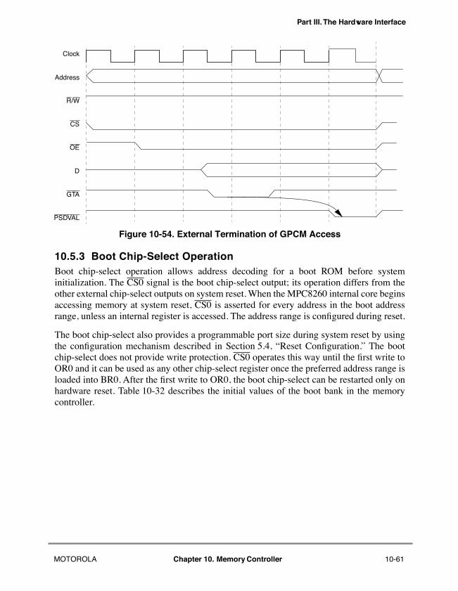
Part III. The Hardware Interface
Figure 10-54. External Termination of GPCM Access
10.5.3 Boot Chip-Select OperationBoot chip-select operation allows address decoding for a boot ROM before systeminitialization. The CS0 signal is the boot chip-select output; its operation differs from theother external chip-select outputs on system reset. When the MPC8260 internal core beginsaccessing memory at system reset, CS0 is asserted for every address in the boot addressrange, unless an internal register is accessed. The address range is conÞgured during reset.
The boot chip-select also provides a programmable port size during system reset by usingthe conÞguration mechanism described in Section 5.4, ÒReset ConÞguration.Ó The bootchip-select does not provide write protection. CS0 operates this way until the Þrst write toOR0 and it can be used as any other chip-select register once the preferred address range isloaded into BR0. After the Þrst write to OR0, the boot chip-select can be restarted only onhardware reset. Table 10-32 describes the initial values of the boot bank in the memorycontroller.
Clock
Address
R/W
CS
OE
D
GTA
PSDVAL
MOTOROLA Chapter 10. Memory Controller 10-61
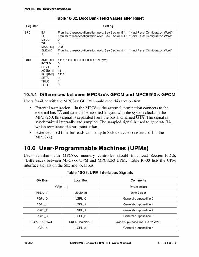
Part III. The Hardware Interface
10.5.4 Differences between MPC8xxÕs GPCM and MPC8260Õs GPCMUsers familiar with the MPC8xx GPCM should read this section Þrst:
¥ External terminationÑIn the MPC8xx the external termination connects to the external bus TA and so must be asserted in sync with the system clock. In the MPC8260, this signal is separated from the bus and named GTA. The signal is synchronized internally and sampled. The sampled signal is used to generate TA, which terminates the bus transaction.
¥ Extended hold time for reads can be up to 8 clock cycles (instead of 1 in the MPC8xx).
10.6 User-Programmable Machines (UPMs)Users familiar with MPC8xx memory controller should Þrst read Section 10.6.6,ÒDifferences between MPC8xx UPM and MPC8260 UPM.Ó Table 10-33 lists the UPMinterface signals on the 60x and local bus.
Table 10-32. Boot Bank Field Values after Reset
Register Setting
BR0 BA From hard reset conÞguration word. See Section 5.4.1, ÒHard Reset ConÞguration Word.ÓPS From hard reset conÞguration word. See Section 5.4.1, ÒHard Reset ConÞguration WordÓDECC 0WP 0MS[0Ð12] 000EMEMC From hard reset conÞguration word. See Section 5.4.1, ÒHard Reset ConÞguration WordÓV 1
OR0 AM[0Ð16] 1111_1110_0000_0000_0 (32 MByte)BCTLD 0CSNT 1ACS[0Ð1] 11SCY[0Ð3] 1111SETA 0TRLX 1EHTR 0
Table 10-33. UPM Interfaces Signals
60x Bus Local Bus Comments
CS[0Ð11] Device select
PBS[0Ð7] LBS[0Ð3] Byte Select
PGPL_0 LGPL_0 General-purpose line 0
PGPL_1 LGPL_1 General-purpose line 1
PGPL_2 LGPL_2 General-purpose line 2
PGPL_3 LGPL_3 General-purpose line 3
PGPL_4/UPWAIT LGPL_4/UPWAIT General-purpose line 4/UPM WAIT
PGPL_5 LGPL_5 General-purpose line 5
10-62 MPC8260 PowerQUICC II UserÕs Manual MOTOROLA
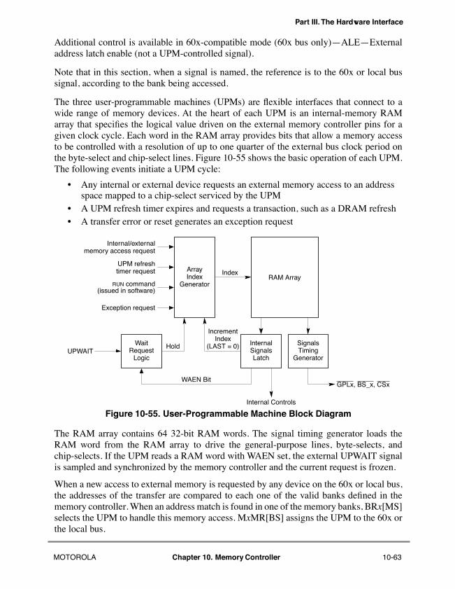
Part III. The Hardware Interface
Additional control is available in 60x-compatible mode (60x bus only)ÑALEÑExternaladdress latch enable (not a UPM-controlled signal).
Note that in this section, when a signal is named, the reference is to the 60x or local bussignal, according to the bank being accessed.
The three user-programmable machines (UPMs) are ßexible interfaces that connect to awide range of memory devices. At the heart of each UPM is an internal-memory RAMarray that speciÞes the logical value driven on the external memory controller pins for agiven clock cycle. Each word in the RAM array provides bits that allow a memory accessto be controlled with a resolution of up to one quarter of the external bus clock period onthe byte-select and chip-select lines. Figure 10-55 shows the basic operation of each UPM.The following events initiate a UPM cycle:
¥ Any internal or external device requests an external memory access to an address space mapped to a chip-select serviced by the UPM
¥ A UPM refresh timer expires and requests a transaction, such as a DRAM refresh¥ A transfer error or reset generates an exception request
Figure 10-55. User-Programmable Machine Block Diagram
The RAM array contains 64 32-bit RAM words. The signal timing generator loads theRAM word from the RAM array to drive the general-purpose lines, byte-selects, andchip-selects. If the UPM reads a RAM word with WAEN set, the external UPWAIT signalis sampled and synchronized by the memory controller and the current request is frozen.
When a new access to external memory is requested by any device on the 60x or local bus,the addresses of the transfer are compared to each one of the valid banks deÞned in thememory controller. When an address match is found in one of the memory banks, BRx[MS]selects the UPM to handle this memory access. MxMR[BS] assigns the UPM to the 60x orthe local bus.
RUN command
UPM refreshtimer request Array
IndexGenerator
Internal/externalmemory access request
Exception request
Index
SignalsTiming
Generator
InternalSignalsLatch
WaitRequest
Logic
RAM Array
UPWAIT
WAEN Bit
Internal Controls
GPLx, BS_x, CSx
IncrementIndex
(LAST = 0)Hold
(issued in software)
MOTOROLA Chapter 10. Memory Controller 10-63
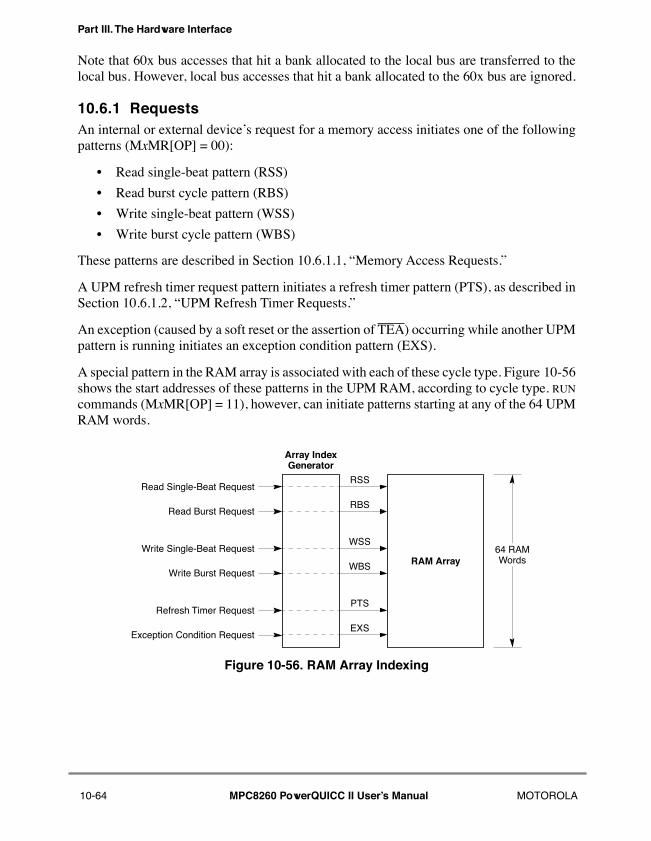
Part III. The Hardware Interface
Note that 60x bus accesses that hit a bank allocated to the local bus are transferred to thelocal bus. However, local bus accesses that hit a bank allocated to the 60x bus are ignored.
10.6.1 RequestsAn internal or external deviceÕs request for a memory access initiates one of the followingpatterns (MxMR[OP] = 00):
¥ Read single-beat pattern (RSS)
¥ Read burst cycle pattern (RBS)
¥ Write single-beat pattern (WSS)
¥ Write burst cycle pattern (WBS)
These patterns are described in Section 10.6.1.1, ÒMemory Access Requests.Ó
A UPM refresh timer request pattern initiates a refresh timer pattern (PTS), as described inSection 10.6.1.2, ÒUPM Refresh Timer Requests.Ó
An exception (caused by a soft reset or the assertion of TEA) occurring while another UPMpattern is running initiates an exception condition pattern (EXS).
A special pattern in the RAM array is associated with each of these cycle type. Figure 10-56shows the start addresses of these patterns in the UPM RAM, according to cycle type. RUN
commands (MxMR[OP] = 11), however, can initiate patterns starting at any of the 64 UPMRAM words.
Figure 10-56. RAM Array Indexing
Write Single-Beat Request
Read Burst Request
Read Single-Beat Request
Write Burst RequestRAM Array
Refresh Timer Request
Exception Condition Request
RSS
RBS
WSS
WBS
PTS
EXS
64 RAMWords
Array IndexGenerator
10-64 MPC8260 PowerQUICC II UserÕs Manual MOTOROLA
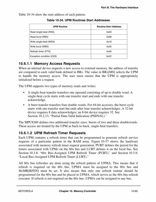
Part III. The Hardware Interface
Table 10-34 show the start address of each pattern.
10.6.1.1 Memory Access RequestsWhen an internal device requests a new access to external memory, the address of transferare compared to each valid bank deÞned in BRx. The value in BRx[MS] selects the UPMto handle the memory access. The user must ensure that the UPM is appropriatelyinitialized before a request.
The UPM supports two types of memory reads and writes:
¥ A single-beat transfer transfers one operand consisting of up to double word. A single-beat cycle starts with one transfer start and ends with one transfer acknowledge.
¥ A burst transfer transfers four double words. For 64-bit accesses, the burst cycle starts with one transfer start but ends after four transfer acknowledges. A 32-bit device requires 8 data acknowledges; an 8-bit device requires 32. See Section 10.2.13, ÒPartial Data Valid Indication (PSDVAL).Ó
The MPC8260 deÞnes two additional transfer sizes: bursts of two and three doublewords.These access are treated by the UPM as back-to-back, single-beat transfers.
10.6.1.2 UPM Refresh Timer RequestsEach UPM contains a refresh timer that can be programmed to generate refresh servicerequests of a particular pattern in the RAM array. Figure 10-57 shows the hardwareassociated with memory refresh timer request generation. PURT deÞnes the period for thetimers associated with UPMx on the 60x bus and LURT deÞnes it on the local bus. SeeSection 10.3.8, Ò60x Bus-Assigned UPM Refresh Timer (PURT),Ó and Section 10.3.9,ÒLocal Bus-Assigned UPM Refresh Timer (LURT).Ó
All 60x bus refreshes are done using the refresh pattern of UPMA. This means that ifrefresh is required on the 60x bus, UPMA must be assigned to the 60x bus andMxMR[RFEN] must be set. It also means that only one refresh routine should beprogrammed for the 60x bus and be placed in UPMA, which serves as the 60x bus refreshexecutor. If refresh is not required on the 60x bus, UPMA can be assigned to any bus.
Table 10-34. UPM Routines Start Addresses
UPM Routine Routine Start Address
Read single-beat (RSS) 0x00
Read burst (RBS) 0x08
Write single-beat (WSS) 0x18
Write burst (WBS) 0x20
Refresh timer (PTS) 0x30
Exception condition (EXS) 0x3C
MOTOROLA Chapter 10. Memory Controller 10-65
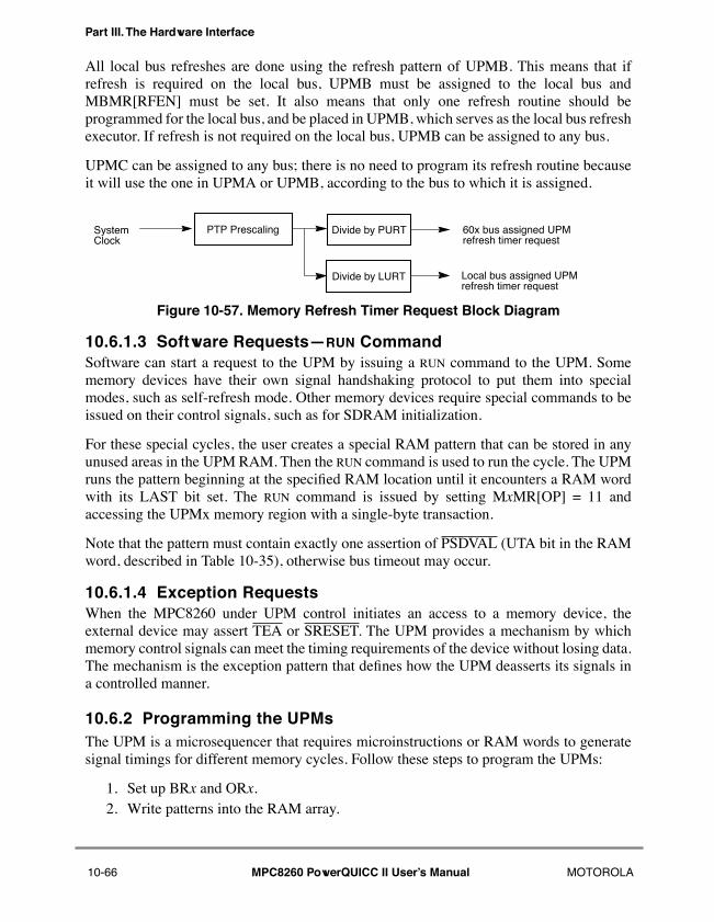
Part III. The Hardware Interface
All local bus refreshes are done using the refresh pattern of UPMB. This means that ifrefresh is required on the local bus, UPMB must be assigned to the local bus andMBMR[RFEN] must be set. It also means that only one refresh routine should beprogrammed for the local bus, and be placed in UPMB, which serves as the local bus refreshexecutor. If refresh is not required on the local bus, UPMB can be assigned to any bus.
UPMC can be assigned to any bus; there is no need to program its refresh routine becauseit will use the one in UPMA or UPMB, according to the bus to which it is assigned.
Figure 10-57. Memory Refresh Timer Request Block Diagram
10.6.1.3 Software RequestsÑRUN CommandSoftware can start a request to the UPM by issuing a RUN command to the UPM. Somememory devices have their own signal handshaking protocol to put them into specialmodes, such as self-refresh mode. Other memory devices require special commands to beissued on their control signals, such as for SDRAM initialization.
For these special cycles, the user creates a special RAM pattern that can be stored in anyunused areas in the UPM RAM. Then the RUN command is used to run the cycle. The UPMruns the pattern beginning at the speciÞed RAM location until it encounters a RAM wordwith its LAST bit set. The RUN command is issued by setting MxMR[OP] = 11 andaccessing the UPMx memory region with a single-byte transaction.
Note that the pattern must contain exactly one assertion of PSDVAL (UTA bit in the RAMword, described in Table 10-35), otherwise bus timeout may occur.
10.6.1.4 Exception RequestsWhen the MPC8260 under UPM control initiates an access to a memory device, theexternal device may assert TEA or SRESET. The UPM provides a mechanism by whichmemory control signals can meet the timing requirements of the device without losing data.The mechanism is the exception pattern that deÞnes how the UPM deasserts its signals ina controlled manner.
10.6.2 Programming the UPMsThe UPM is a microsequencer that requires microinstructions or RAM words to generatesignal timings for different memory cycles. Follow these steps to program the UPMs:
1. Set up BRx and ORx.2. Write patterns into the RAM array.
60x bus assigned UPM
Local bus assigned UPM
System Divide by PURTPTP Prescaling
Divide by LURT
refresh timer request
refresh timer request
Clock
10-66 MPC8260 PowerQUICC II UserÕs Manual MOTOROLA
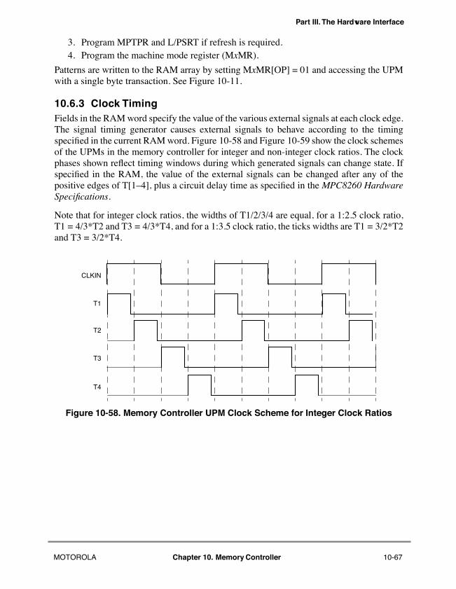
Part III. The Hardware Interface
3. Program MPTPR and L/PSRT if refresh is required.4. Program the machine mode register (MxMR).
Patterns are written to the RAM array by setting MxMR[OP] = 01 and accessing the UPMwith a single byte transaction. See Figure 10-11.
10.6.3 Clock TimingFields in the RAM word specify the value of the various external signals at each clock edge.The signal timing generator causes external signals to behave according to the timingspeciÞed in the current RAM word. Figure 10-58 and Figure 10-59 show the clock schemesof the UPMs in the memory controller for integer and non-integer clock ratios. The clockphases shown reßect timing windows during which generated signals can change state. IfspeciÞed in the RAM, the value of the external signals can be changed after any of thepositive edges of T[1Ð4], plus a circuit delay time as speciÞed in the MPC8260 HardwareSpeciÞcations.
Note that for integer clock ratios, the widths of T1/2/3/4 are equal, for a 1:2.5 clock ratio,T1 = 4/3*T2 and T3 = 4/3*T4, and for a 1:3.5 clock ratio, the ticks widths are T1 = 3/2*T2and T3 = 3/2*T4.
Figure 10-58. Memory Controller UPM Clock Scheme for Integer Clock Ratios
CLKIN
T1
T2
T3
T4
MOTOROLA Chapter 10. Memory Controller 10-67
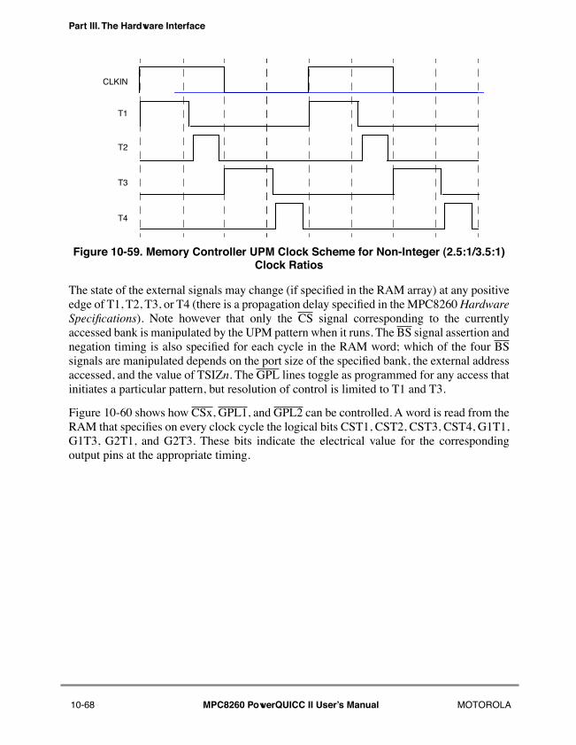
Part III. The Hardware Interface
Figure 10-59. Memory Controller UPM Clock Scheme for Non-Integer (2.5:1/3.5:1) Clock Ratios
The state of the external signals may change (if speciÞed in the RAM array) at any positiveedge of T1, T2, T3, or T4 (there is a propagation delay speciÞed in the MPC8260 HardwareSpeciÞcations). Note however that only the CS signal corresponding to the currentlyaccessed bank is manipulated by the UPM pattern when it runs. The BS signal assertion andnegation timing is also speciÞed for each cycle in the RAM word; which of the four BSsignals are manipulated depends on the port size of the speciÞed bank, the external addressaccessed, and the value of TSIZn. The GPL lines toggle as programmed for any access thatinitiates a particular pattern, but resolution of control is limited to T1 and T3.
Figure 10-60 shows how CSx, GPL1, and GPL2 can be controlled. A word is read from theRAM that speciÞes on every clock cycle the logical bits CST1, CST2, CST3, CST4, G1T1,G1T3, G2T1, and G2T3. These bits indicate the electrical value for the correspondingoutput pins at the appropriate timing.
CLKIN
T1
T2
T3
T4
10-68 MPC8260 PowerQUICC II UserÕs Manual MOTOROLA
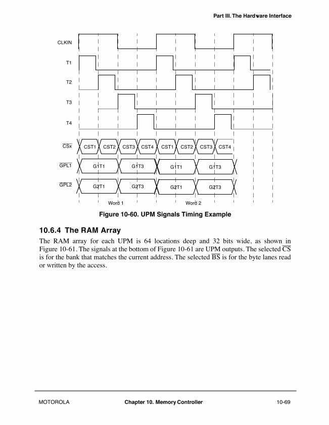
Part III. The Hardware Interface
Figure 10-60. UPM Signals Timing Example
10.6.4 The RAM ArrayThe RAM array for each UPM is 64 locations deep and 32 bits wide, as shown inFigure 10-61. The signals at the bottom of Figure 10-61 are UPM outputs. The selected CSis for the bank that matches the current address. The selected BS is for the byte lanes reador written by the access.
CSx
GPL1
GPL2
CST1 CST2 CST3 CST4 CST1 CST2 CST3 CST4
G1T1 G1T3
Word 1 Word 2
CLKIN
T1
T2
T3
T4
G1T1 G1T3
G2T1 G2T3 G2T1 G2T3
MOTOROLA Chapter 10. Memory Controller 10-69
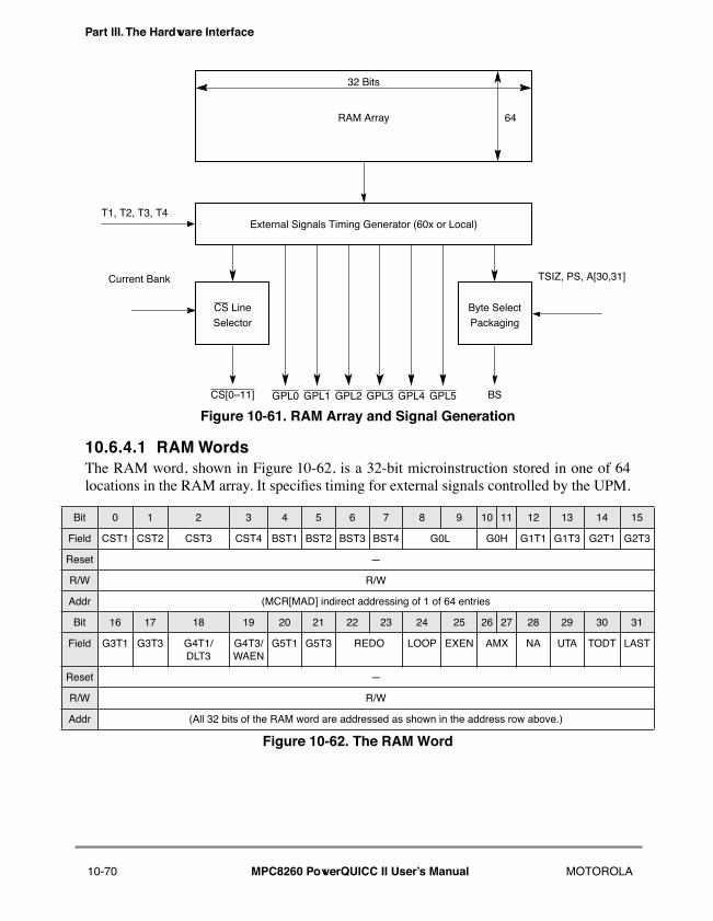
Part III. The Hardware Interface
B
F 3
Re
R
A
B
F T
Re
R
A
Figure 10-61. RAM Array and Signal Generation
10.6.4.1 RAM WordsThe RAM word, shown in Figure 10-62, is a 32-bit microinstruction stored in one of 64locations in the RAM array. It speciÞes timing for external signals controlled by the UPM.
it 0 1 2 3 4 5 6 7 8 9 10 11 12 13 14 15
ield CST1 CST2 CST3 CST4 BST1 BST2 BST3 BST4 G0L G0H G1T1 G1T3 G2T1 G2T
set Ñ
/W R/W
ddr (MCR[MAD] indirect addressing of 1 of 64 entries
it 16 17 18 19 20 21 22 23 24 25 26 27 28 29 30 31
ield G3T1 G3T3 G4T1/DLT3
G4T3/WAEN
G5T1 G5T3 REDO LOOP EXEN AMX NA UTA TODT LAS
set Ñ
/W R/W
ddr (All 32 bits of the RAM word are addressed as shown in the address row above.)
Figure 10-62. The RAM Word
T1, T2, T3, T4
GPL0 GPL2 GPL3 GPL4 GPL5
External Signals Timing Generator (60x or Local)
RAM Array
CS LineSelector
Byte SelectPackaging
CS[0Ð11] BS
Current Bank TSIZ, PS, A[30,31]
32 Bits
64
GPL1
10-70 MPC8260 PowerQUICC II UserÕs Manual MOTOROLA
Part III. The Hardware Interface
Table 10-35 describes RAM word Þelds.
Table 10-35. RAM Word Bit Settings
Bit Name Description
0 CST1 Chip-select timing 1. DeÞnes the state of CS during clock phase 1.0 The value of the CS line at the rising edge of T1 will be 01 The value of the CS line at the rising edge of T1 will be 1See Section 10.6.4.1.1, ÒChip-Select Signals (CxTx).Ó
1 CST2 Chip-select timing 2. DeÞnes the state of CS during clock phase 2.0 The value of the CS line at the rising edge of T2 will be 01 The value of the CS line at the rising edge of T2 will be 1
2 CST3 Chip-select timing 3. DeÞnes the state of CS during clock phase 3.0 The value of the CS line at the rising edge of T3 will be 01 The value of the CS line at the rising edge of T3 will be 1
3 CST4 Chip-select timing4. DeÞnes the state of CS during clock phase 4.0 The value of the CS line at the rising edge of T4 will be 01 The value of the CS line at the rising edge of T4 will be 1
4 BST1 Byte-select timing 1. DeÞnes the state of BS during clock phase 1.0 The value of the BS lines at the rising edge of T2 will be 01 The value of the BS lines at the rising edge of T2 will be 1The Þnal value of the BS lines depends on the values of BRx[PS], the TSIZ lines, and A[30Ð31] for the access. See Section 10.6.4.1.2, ÒByte-Select Signals (BxTx).Ó
5 BST2 Byte-select timing 2. DeÞnes the state of BS during clock phase 2.0 The value of the BS lines at the rising edge of T2 will be 01 The value of the BS lines at the rising edge of T2 will be 1The Þnal value of the BS lines depends on the values of BRx[PS], TSIZx, and A[30Ð31] for the access.
6 BST3 Byte-select timing 3. DeÞnes the state of BS during clock phase 3.0 The value of the BS lines at the rising edge of T3 will be 01 The value of the BS lines at the rising edge of T3 will be 1The Þnal value of the BS lines depends on the values of BRx[PS], TSIZx, and A[30Ð31] for the access.
7 BST4 Byte-select timing 4. DeÞnes the state of BS during clock phase 4.0 The value of the BS lines at the rising edge of T4 will be 01 The value of the BS lines at the rising edge of T4 will be 1The Þnal value of the BS lines depends on the values of BRx[PS], TSIZx, and A[30Ð31] for the access.
8Ð9 G0L General-purpose line 0 lower. DeÞnes the state of GPL0 during phases 1Ð2.00 The value of GPL0 at the rising edge of T1 is as deÞned in MxMR[G0CL] 10 The value of the GPL0 line at the rising edge of T1 will be 011 The value of the GPL0 line at the rising edge of T1 will be 1See Section 10.6.4.1.3, ÒGeneral-Purpose Signals (GxTx, GOx).Ó
10Ð11 G0H General-purpose line 0 higher. DeÞnes the state of GPL0 during phase 3Ð4.00 The value of GPL0 at the rising edge of T3 is as deÞned in MxMR[G0CL]10 The value of the GPL0 line at the rising edge of T3 will be 011 The value of the GPL0 line at the rising edge of T3 will be 1See Section 10.6.4.1.3, ÒGeneral-Purpose Signals (GxTx, GOx).Ó
MOTOROLA Chapter 10. Memory Controller 10-71
Part III. The Hardware Interface
12 G1T1 General-purpose line 1 timing 1. DeÞnes the state of GPL1 during phase 1Ð2.0 The value of the GPL0 line at the rising edge of T1 will be 01 The value of the GPL0 line at the rising edge of T1 will be 1See Section 10.6.4.1.3, ÒGeneral-Purpose Signals (GxTx, GOx).Ó
13 G1T3 General-purpose line 1 timing 3. DeÞnes the state of GPL1 during phase 3Ð4.0 The value of the GPL1 line at the rising edge of T3 will be 01 The value of the GPL1 line at the rising edge of T3 will be 1See Section 10.6.4.1.3, ÒGeneral-Purpose Signals (GxTx, GOx).Ó
14 G2T1 General-purpose line 2 timing 1. DeÞnes the state of GPL2 during phase 1Ð2.0 The value of the GPL2 line at the rising edge of T1 will be 01 The value of the GPL2 line at the rising edge of T1 will be 1See Section 10.6.4.1.3, ÒGeneral-Purpose Signals (GxTx, GOx).Ó
15 G2T3 General-purpose line 2 timing 3. DeÞnes the state of GPL2 during phase 3Ð4.0 The value of the GPL2 line at the rising edge of T3 will be 01 The value of the GPL2 line at the rising edge of T3 will be 1See Section 10.6.4.1.3, ÒGeneral-Purpose Signals (GxTx, GOx).Ó
16 G3T1 General-purpose line 3 timing 1. DeÞnes the state of GPL3 during phase 1Ð2.0 The value of the GPL3 line at the rising edge of T1 will be 01The value of the GPL3 line at the rising edge of T1 will be 1See Section 10.6.4.1.3, ÒGeneral-Purpose Signals (GxTx, GOx).Ó
17 G3T3 General-purpose line 3 timing 3. DeÞnes the state of GPL3 during phase 3Ð4.0 The value of the GPL3 line at the rising edge of T3 will be 01 The value of the GPL3 line at the rising edge of T3 will be 1See Section 10.6.4.1.3, ÒGeneral-Purpose Signals (GxTx, GOx).Ó
18 G4T/DLT2
General-purpose line 4 timing 1/delay time 2. The function is determined by MxMR[GPLx4DIS].
G4T1 If MxMR deÞnes UPWAITx/GPL_x4 as an output (GPL_x4), this bit functions as G4T1:0 The value of the GPL4 line at the rising edge of T1 will be 01 The value of the GPL4 line at the rising edge of T1 will be 1See Section 10.6.4.1.3, ÒGeneral-Purpose Signals (GxTx, GOx).Ó
DLT3 If MxMR[GPLx4DIS] = 1, UPWAITx is chosen and this bit functions as DLT3.0 In the current word, indicates that the data bus should be sampled at the rising edge of T1 (if a read
burst or a single read service is executed).1 In the current word, indicates that the data bus should be sampled at the rising edge of T3 (if a read
burst or a single read service is executed).For an example, see Section 10.6.4.3, ÒData Valid and Data Sample Control.Ó
19 G4T3/WAEN
General-purpose line 4 timing 3/wait enable. Function depends on the value of MxMR[GPLx4DIS].
G4T3 If MxMR[GPLx4DIS] = 0, G4T3 is selected.0 The value of the GPL4 line at the rising edge of T3 will be 01 The value of the GPL4 line at the rising edge of T3 will be 1
WAEN If MxMR[GPLx4DIS] = 1, WAEN is selected. See Section 10.6.4.5, ÒThe Wait Mechanism.Ó0 The UPWAITx function is disabled.1 A freeze in the external signals logical value occurs if the external WAIT signal is detected
asserted. This condition lasts until WAIT is negated.
Table 10-35. RAM Word Bit Settings (Continued)
Bit Name Description
10-72 MPC8260 PowerQUICC II UserÕs Manual MOTOROLA
Part III. The Hardware Interface
20 G5T1 General-purpose line 5 timing 1. DeÞnes the state of GPL5 during phase 1Ð2.0 The value of the GPL5 line at the rising edge of T1 will be 01 The value of the GPL5 line at the rising edge of T1 will be 1
21 G5T3 General-purpose line 5 timing 3. DeÞnes the state of GPL5 during phase 3Ð4.0 The value of the GPL5 line at the rising edge of T3 will be 01 The value of the GPL5 line at the rising edge of T3 will be 1
22Ð23 Ñ Redo current RAM word. See ÒSection 10.6.4.1.5, ÒRepeat Execution of Current RAM Word (REDO).Ó00 Normal operation01 The current RAM word is executed twice.10 The current RAM word is executed tree times.11 The current RAM word is executed four times.
24 LOOP Loop. The Þrst RAM word in the RAM array where LOOP is 1 is recognized as the loop start word. The next RAM word where LOOP is 1 is the loop end word. RAM words between the start and end are deÞned as the loop. The number of times the UPM executes this loop is deÞned in the corresponding loop Þeld of the MxMR.0 The current RAM word is not the loop start word or loop end word. 1 The current RAM word is the start or end of a loop. See Section 10.6.4.1.4, ÒLoop Control.Ó
25 EXEN Exception enable. If an external device asserts TEA or RESET, EXEN allows branching to an exception pattern at the exception start address (EXS) at a Þxed address in the RAM array.When the MPC8260 under UPM control begins accessing a memory device, the external device may assert TEA or SRESET. An exception occurs when one of these signals is asserted by an external device and the MPC8260 begins closing the memory cycle transfer. When one of these exceptions is recognized and EXEN in the RAM word is set, the UPM branches to the special exception start address (EXS) and begins operating as the pattern deÞned there speciÞes. See Table 10-34. The user should provide an exception pattern to deassert signals controlled by the UPM in a controlled fashion. For DRAM control, a handler should negate RAS and CAS to prevent data corruption. If EXEN = 0, exceptions are deferred and execution continues. After the UPM branches to the exception start address, it continues reading until the LAST bit is set in the RAM word.0 The UPM continues executing the remaining RAM words.1 The current RAM word allows a branch to the exception pattern after the current cycle if an
exception condition is detected. The exception condition can be an external device asserting TEA or SRESET.
26Ð27 AMX Address multiplexing. Determines the source of A[0Ð31] at the rising edge of t1 (single-MPC8260 mode only). See Section 10.6.4.2, ÒAddress Multiplexing.Ó 00 A[0Ð31] is the non-multiplexed address. For example, column address.01 Reserved.10 A[0Ð31] is the address requested by the internal master multiplexed according to MxMR[AMx].
For example, row address.11 A[0Ð31] is the contents of MAR. Used for example, during SDRAM mode initialization.
28 NA Next address. Determines when the address is incremented during a burst access.0 The address increment function is disabled1 The address is incremented in the next cycle. In conjunction with the BRx[PS], the increment value
of A[27Ð31] and/or BADDR[27Ð31] at the rising edge of T1 is as followsIf the accessed bank has a 64-bit port size, the value is incremented by 8.If the accessed bank has a 32-bit port size, the value is incremented by 4.If the accessed bank has a 16-bit port size, the value is incremented by 2.If the accessed bank has an 8-bit port size, the value is incremented by 1.
Note: The value of NA is relevant only when the UPM serves a burst-read or burst-write request. NA is reserved under other patterns.
Table 10-35. RAM Word Bit Settings (Continued)
Bit Name Description
MOTOROLA Chapter 10. Memory Controller 10-73
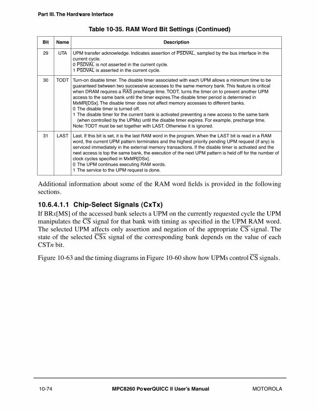
Part III. The Hardware Interface
Additional information about some of the RAM word Þelds is provided in the followingsections.
10.6.4.1.1 Chip-Select Signals (CxTx)If BRx[MS] of the accessed bank selects a UPM on the currently requested cycle the UPMmanipulates the CS signal for that bank with timing as speciÞed in the UPM RAM word.The selected UPM affects only assertion and negation of the appropriate CS signal. Thestate of the selected CSx signal of the corresponding bank depends on the value of eachCSTn bit.
Figure 10-63 and the timing diagrams in Figure 10-60 show how UPMs control CS signals.
29 UTA UPM transfer acknowledge. Indicates assertion of PSDVAL, sampled by the bus interface in the current cycle.0 PSDVAL is not asserted in the current cycle.1 PSDVAL is asserted in the current cycle.
30 TODT Turn-on disable timer. The disable timer associated with each UPM allows a minimum time to be guaranteed between two successive accesses to the same memory bank. This feature is critical when DRAM requires a RAS precharge time. TODT, turns the timer on to prevent another UPM access to the same bank until the timer expires.The disable timer period is determined in MxMR[DSx]. The disable timer does not affect memory accesses to different banks. 0 The disable timer is turned off.1 The disable timer for the current bank is activated preventing a new access to the same bank
(when controlled by the UPMs) until the disable timer expires. For example, precharge time.Note: TODT must be set together with LAST. Otherwise it is ignored.
31 LAST Last. If this bit is set, it is the last RAM word in the program. When the LAST bit is read in a RAM word, the current UPM pattern terminates and the highest priority pending UPM request (if any) is serviced immediately in the external memory transactions. If the disable timer is activated and the next access is top the same bank, the execution of the next UPM pattern is held off for the number of clock cycles speciÞed in MxMR[DSx].0 The UPM continues executing RAM words.1 The service to the UPM request is done.
Table 10-35. RAM Word Bit Settings (Continued)
Bit Name Description
10-74 MPC8260 PowerQUICC II UserÕs Manual MOTOROLA
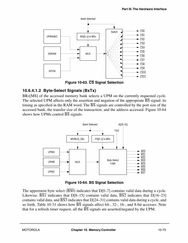
Part III. The Hardware Interface
Figure 10-63. CS Signal Selection
10.6.4.1.2 Byte-Select Signals (BxTx)BRx[MS] of the accessed memory bank selects a UPM on the currently requested cycle.The selected UPM affects only the assertion and negation of the appropriate BS signal; itstiming as speciÞed in the RAM word. The BS signals are controlled by the port size of theaccessed bank, the transfer size of the transaction, and the address accessed. Figure 10-64shows how UPMs control BS signals.
Figure 10-64. BS Signal Selection
The uppermost byte select (BS0) indicates that D[0Ð7] contains valid data during a cycle.Likewise, BS1 indicates that D[8Ð15] contains valid data, BS2 indicates that D[16Ð23]contains valid data, and BS3 indicates that D[24Ð31] contains valid data during a cycle, andso forth. Table 10-31 shows how BS signals affect 64-, 32-, 16-, and 8-bit accesses. Notethat for a refresh timer request, all the BS signals are asserted/negated by the UPM.
UPMA/B/C
SDRAM
GPCM
MUX
MS[0–1] in BRx
CS3
CS4
CS5
CS6
CS7
CS8
Switch
Bank Selected
CS9
CS10
CS11
CS0
CS1
CS2
UPMA
MUX
MS/BUS_SEL
BS0BS1BS2BS3
Bank Selected
PS[0–1] in BRx
A[29–31]
TSIZ
Byte-SelectLogicUPMB
UPMC
BS4BS5BS6BS7
MOTOROLA Chapter 10. Memory Controller 10-75
Part III. The Hardware Interface
10.6.4.1.3 General-Purpose Signals (GxTx, GOx)The general-purpose signals (GPL[1Ð5]) each have two bits in the RAM word that deÞnethe logical value of the signal to be changed at the rising edge of T1 and/or at the rising edgeof T3. GPL0 offer enhancements beyond the other GPLx lines.
GPL0 can be controlled by an address line speciÞed in MxMR[G0CLx]. To use this feature,set G0H and G0L in the RAM word. For example, for a SIMM with multiple banks, thisaddress line can be used to switch between banks.
10.6.4.1.4 Loop Control The LOOP bit in the RAM word (bit 24) speciÞes the beginning and end of a set of UPMRAM words that are to be repeated. The Þrst time LOOP = 1, the memory controllerrecognizes it as a loop start word and loads the memory loop counter with thecorresponding contents of the loop Þeld shown in Table 10-36. The next RAM word forwhich LOOP = 1 is recognized as a loop end word. When it is reached, the loop counter isdecremented by one.
Continued loop execution depends on the loop counter. If the counter is not zero, the nextRAM word executed is the loop start word. Otherwise, the next RAM word executed is theone after the loop end word. Loops can be executed sequentially but cannot be nested.
10.6.4.1.5 Repeat Execution of Current RAM Word (REDO) The REDO function is useful for wait-state insertion in a long UPM routine that wouldotherwise need too many RAM words. Setting the REDO bits of the RAM word to anonzero value to cause the UPM to reexecute the current RAM word up to three times,according to Table 10-35.
Special care must be taken in the following cases:
¥ When UTA and REDO are set together, PSDVAL is asserted the number of times speciÞed by the REDO function.
¥ When LOOP and REDO are set together, the loop mechanism works as usual and the line is repeated according to the REDO function.
¥ LAST and REDO should not be set together.¥ REDO should not be used within the exception routine.
Table 10-36. MxMR Loop Field Usage
Request Serviced Loop Field
Read single-beat cycle RLFx
Read burst cycle RLFx
Write single-beat cycle WLFx
Write burst cycle WLFx
Refresh timer expired TLFx
RUN command RLFx
10-76 MPC8260 PowerQUICC II UserÕs Manual MOTOROLA
Part III. The Hardware Interface
Figure 10-79 shows an example of REDO use.
10.6.4.2 Address Multiplexing The address lines can be controlled by the pattern the user provides in the UPM. Theaddress multiplex bits can choose between outputting an address requested by the internalmaster as is and outputting it according to the multiplexing speciÞed by the MxMR[AMx].The last option is to output the contents of the MAR on the address pins.
Note that in 60x-compatible mode, MAR cannot be output on the 60x bus external addressline.
Note that on the local bus, only the lower 18 bits of the MAR are output.
Table 10-37 shows how MxMR[AMx] settings affect address multiplexing.
See Section 10.6.5, ÒUPM DRAM ConÞguration Example,Ó for more details.
10.6.4.3 Data Valid and Data Sample Control When a read access is handled by the UPM and the UTA bit is 1, the value of the DLT3 bitin the same RAM word indicates when the data input is sampled by the internal bus master,assuming that MxMR[GPLx4DIS] = 1.
¥ If G4T4/DLT3 functions as DLT3 and DLT3 = 1 in the RAM word, data is latched on the falling edge of CLKIN instead of the rising edge. The data is sampled by the internal master on the next rising edge as is required by the MPC8260 bus operation spec. This feature lets the user speed up the memory interface by latching data 1/2 clock early, which can be useful during burst reads. This feature should be used only in systems without external synchronous bus devices.
¥ If G4T4/DLT3 functions as G4T4, data is latched on the rising edge of CLKIN, as is normal in MPC8260 bus operation.
Figure 10-65 shows data sampling that is controlled by the UPM.
Table 10-37. UPM Address Multiplexing
AMxExternal Bus Address Pin
A16 A17 A18 A19 A20 A21 A22 A23 A24 A25 A26 A27 A28 A29 A30 A31
000
Signal Driven on External Pin when Address Multiplexing is Enabled
A8 A9 A10 A11 A12 A13 A14 A15 A16 A17 A18 A19 A20 A21 A22 A23
001 A7 A8 A9 A10 A11 A12 A13 A14 A15 A16 A17 A18 A19 A20 A21 A22
010 A6 A7 A8 A9 A10 A11 A12 A13 A14 A15 A16 A17 A18 A19 A20 A21
011 A5 A6 A7 A8 A9 A10 A11 A12 A13 A14 A15 A16 A17 A18 A19 A20
100 Ñ A5 A6 A7 A8 A9 A10 A11 A12 A13 A14 A15 A16 A17 A18 A19
101 Ñ Ñ A5 A6 A7 A8 A9 A10 A11 A12 A13 A14 A15 A16 A17 A18
MOTOROLA Chapter 10. Memory Controller 10-77
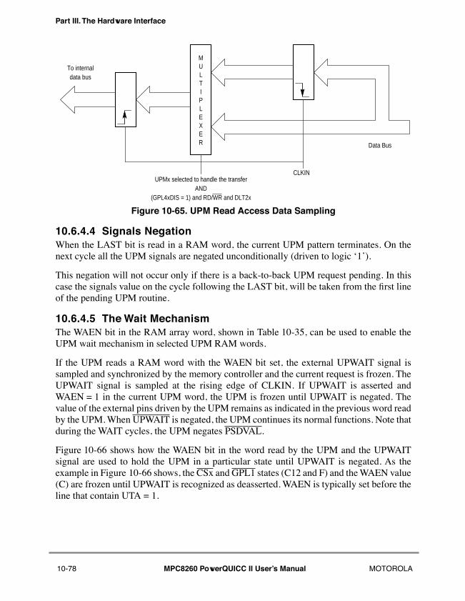
Part III. The Hardware Interface
Figure 10-65. UPM Read Access Data Sampling
10.6.4.4 Signals NegationWhen the LAST bit is read in a RAM word, the current UPM pattern terminates. On thenext cycle all the UPM signals are negated unconditionally (driven to logic Ô1Õ).
This negation will not occur only if there is a back-to-back UPM request pending. In thiscase the signals value on the cycle following the LAST bit, will be taken from the Þrst lineof the pending UPM routine.
10.6.4.5 The Wait Mechanism The WAEN bit in the RAM array word, shown in Table 10-35, can be used to enable theUPM wait mechanism in selected UPM RAM words.
If the UPM reads a RAM word with the WAEN bit set, the external UPWAIT signal issampled and synchronized by the memory controller and the current request is frozen. TheUPWAIT signal is sampled at the rising edge of CLKIN. If UPWAIT is asserted andWAEN = 1 in the current UPM word, the UPM is frozen until UPWAIT is negated. Thevalue of the external pins driven by the UPM remains as indicated in the previous word readby the UPM. When UPWAIT is negated, the UPM continues its normal functions. Note thatduring the WAIT cycles, the UPM negates PSDVAL.
Figure 10-66 shows how the WAEN bit in the word read by the UPM and the UPWAITsignal are used to hold the UPM in a particular state until UPWAIT is negated. As theexample in Figure 10-66 shows, the CSx and GPL1 states (C12 and F) and the WAEN value(C) are frozen until UPWAIT is recognized as deasserted. WAEN is typically set before theline that contain UTA = 1.
To internaldata bus
CLKINUPMx selected to handle the transfer
AND(GPL4xDIS = 1) and RD/WR and DLT2x
Data Bus
MULTIPLEXER
10-78 MPC8260 PowerQUICC II UserÕs Manual MOTOROLA
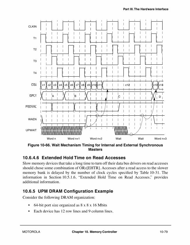
Part III. The Hardware Interface
Figure 10-66. Wait Mechanism Timing for Internal and External Synchronous Masters
10.6.4.6 Extended Hold Time on Read Accesses Slow memory devices that take a long time to turn off their data bus drivers on read accessesshould chose some combination of ORx[EHTR]. Accesses after a read access to the slowermemory bank is delayed by the number of clock cycles speciÞed by Table 10-31. Theinformation in Section 10.5.1.6, ÒExtended Hold Time on Read Accesses,Ó providesadditional information.
10.6.5 UPM DRAM ConÞguration ExampleConsider the following DRAM organization:
¥ 64-bit port size organized as 8 x 8 x 16 Mbits
¥ Each device has 12 row lines and 9 column lines.
CSx
GPL1
WAEN
Word n Word n+1
c1 c2 c3 c4 c5 c6 c7 c8
UPWAIT
c9 c10 c11 c12 c13 c14
Word n+2 Wait Wait Word n+3
PSDVAL
CLKIN
T1
T2
T3
T4
A B C D
MOTOROLA Chapter 10. Memory Controller 10-79

Part III. The Hardware Interface
This means that the address bus should be partitioned as shown in Table 10-38.
From the device perspective, during RAS assertion, its address port should look likeTable 10-39:
Table 10-37 indicates that to multiplex A[8Ð19] over A[17Ð28], choose AMx = 001.
Table 10-40 shows the register conÞguration. Not shown are PURT and MPTPR, whichshould be programmed according to the device refresh requirements.
10.6.6 Differences between MPC8xx UPM and MPC8260 UPMUsers familiar with the MPC8xx UPM should read this section Þrst.
Below is a list of the major differences between the MPC8xx devices and the MPC8260:
¥ First cycle timing transferred to the UPM arrayÑIn the MPC8xxÕs UPM, the Þrst cycle value of some of the signals is determined from ORx[SAM,G5LA,G5LS]. This is eliminated in the MPC8260. All signals are controlled only by the pattern written to the array.
Table 10-38. 60x Address Bus Partition
A[0Ð7] A[8Ð19] A[20Ð28] A[29Ð31]
msb of start address Row Column lsb
Table 10-39. DRAM Device Address Port during an ACTIVATE command
ÒA[0Ð16]Ó A[17Ð28] A[29Ð31]
Ñ Row (A[8Ð19]) n.c.
Table 10-40. Register Settings
Register Settings
BRx BA msb of base address PS 00 = 64-bit port sizeDECC 00WP 0MS 100 = UPMA
EMEMC 0ATOM 00DR 0V 1
ORx AM 1111_1111_0000_0000_0 = 16 MbyteBI 0
EHTR 0
MxMR BSEL 0 = 60x busRFEN 1OP 00AM 001DSA As neededG0CLA N/A
GPL_A4DIS 0RLFA As neededWLFA As neededTLFA As neededMAD N/A
10-80 MPC8260 PowerQUICC II UserÕs Manual MOTOROLA
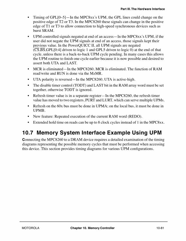
Part III. The Hardware Interface
¥ Timing of GPL[0Ð5]ÑIn the MPC8xxÕs UPM, the GPL lines could change on the positive edge of T2 or T3. In the MPC8260 these signals can change in the positive edge of T1 or T3 to allow connection to high-speed synchronous devices such as burst SRAM.
¥ UPM controlled signals negated at end of an accessÑIn the MPC8xxÕs UPM, if the user did not negate the UPM signals at end of an access, those signals kept their previous value. In the PowerQUICC II, all UPM signals are negated (CS,BS,GPL[0:4] driven to logic 1 and GPL5 driven to logic 0) at the end of that cycle, unless there is a back-to-back UPM cycle pending. In many cases this allows the UPM routine to Þnish one cycle earlier because it is now possible and desired to assert both UTA and LAST.
¥ MCR is eliminatedÑIn the MPC8260, MCR is eliminated. The function of RAM read/write and RUN is done via the MxMR.
¥ UTA polarity is reversedÑIn the MPC8260, UTA is active-high.
¥ The disable timer control (TODT) and LAST bit in the RAM array word must be set together, otherwise TODT is ignored.
¥ Refresh timer value is in a separate registerÑIn the MPC8260, the refresh timer value has moved to two registers, PURT and LURT, which can serve multiple UPMs.
¥ Refresh on the 60x bus must be done in UPMA; on the local bus, it must be done in UPMB.
¥ New feature: Repeated execution of the current RAM word (REDO).
¥ Extended hold time on reads can be up to 8 clock cycles instead of 1 in the MPC8xx.
10.7 Memory System Interface Example Using UPMConnecting the MPC8260 to a DRAM device requires a detailed examination of the timingdiagrams representing the possible memory cycles that must be performed when accessingthis device. This section provides timing diagrams for various UPM conÞgurations.
MOTOROLA Chapter 10. Memory Controller 10-81
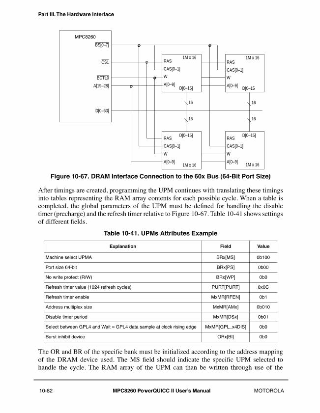
Part III. The Hardware Interface
Figure 10-67. DRAM Interface Connection to the 60x Bus (64-Bit Port Size)
After timings are created, programming the UPM continues with translating these timingsinto tables representing the RAM array contents for each possible cycle. When a table iscompleted, the global parameters of the UPM must be deÞned for handling the disabletimer (precharge) and the refresh timer relative to Figure 10-67. Table 10-41 shows settingsof different Þelds.
The OR and BR of the speciÞc bank must be initialized according to the address mappingof the DRAM device used. The MS Þeld should indicate the speciÞc UPM selected tohandle the cycle. The RAM array of the UPM can than be written through use of the
Table 10-41. UPMs Attributes Example
Explanation Field Value
Machine select UPMA BRx[MS] 0b100
Port size 64-bit BRx[PS] 0b00
No write protect (R/W) BRx[WP] 0b0
Refresh timer value (1024 refresh cycles) PURT[PURT] 0x0C
Refresh timer enable MxMR[RFEN] 0b1
Address multiplex size MxMR[AMx] 0b010
Disable timer period MxMR[DSx] 0b01
Select between GPL4 and Wait = GPL4 data sample at clock rising edge MxMR[GPL_x4DIS] 0b0
Burst inhibit device ORx[BI] 0b0
RAS
CAS[0–1]
W
1M x 16
16
A[0–9]D[0–15]
RAS
CAS[0–1]
W
1M x 16
16
A[0–9]
D[0–15]
MPC8260
BS[0–7]
CS1
BCTL0
A[19–28]
D[0–63]
RAS
CAS[0–1]
W
1M x 16
16
A[0–9]
D[0–15]
RAS
CAS[0–1]
W
1M x 16
16
A[0–9]D[0–15
10-82 MPC8260 PowerQUICC II UserÕs Manual MOTOROLA
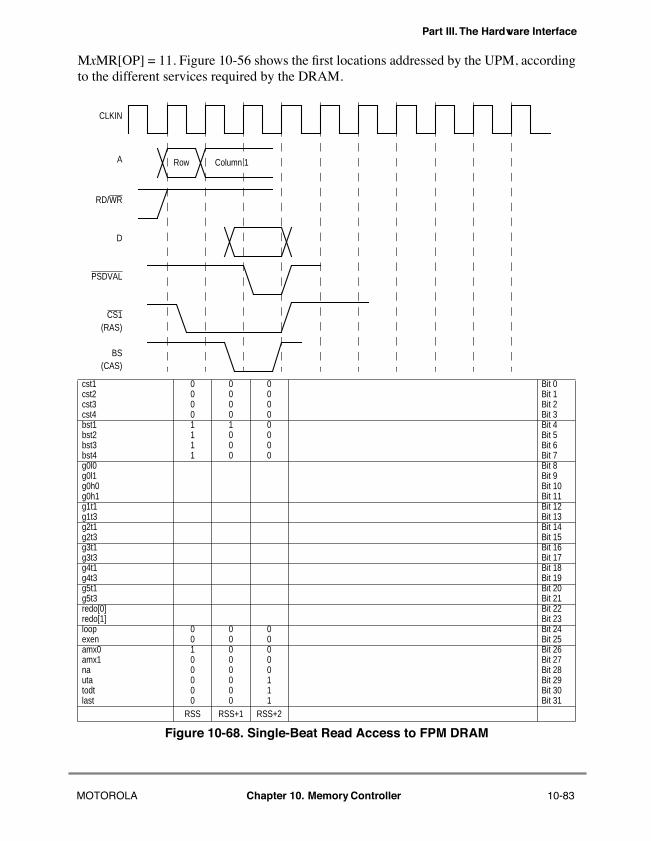
Part III. The Hardware Interface
MxMR[OP] = 11. Figure 10-56 shows the Þrst locations addressed by the UPM, accordingto the different services required by the DRAM.
Figure 10-68. Single-Beat Read Access to FPM DRAM
cst1 0 0 0 Bit 0cst2 0 0 0 Bit 1cst3 0 0 0 Bit 2cst4 0 0 0 Bit 3bst1 1 1 0 Bit 4bst2 1 0 0 Bit 5bst3 1 0 0 Bit 6bst4 1 0 0 Bit 7g0l0 Bit 8g0l1 Bit 9g0h0 Bit 10g0h1 Bit 11g1t1 Bit 12g1t3 Bit 13g2t1 Bit 14g2t3 Bit 15g3t1 Bit 16g3t3 Bit 17g4t1 Bit 18g4t3 Bit 19g5t1 Bit 20g5t3 Bit 21redo[0] Bit 22redo[1] Bit 23loop 0 0 0 Bit 24exen 0 0 0 Bit 25amx0 1 0 0 Bit 26amx1 0 0 0 Bit 27na 0 0 0 Bit 28uta 0 0 1 Bit 29todt 0 0 1 Bit 30last 0 0 1 Bit 31
RSS RSS+1 RSS+2
CLKIN
A
RD/WR
D
PSDVAL
CS1
BS
Row Column 1
(CAS)
(RAS)
MOTOROLA Chapter 10. Memory Controller 10-83

Part III. The Hardware Interface
Figure 10-69. Single-Beat Write Access to FPM DRAM
cst1 0 0 0 Bit 0cst2 0 0 0 Bit 1cst3 0 0 0 Bit 2cst4 0 0 1 Bit 3bst1 1 1 0 Bit 4bst2 1 1 0 Bit 5bst3 1 0 0 Bit 6bst4 1 0 1 Bit 7g0l0 Bit 8g0l1 Bit 9g0h0 Bit 10g0h1 Bit 11g1t1 Bit 12g1t3 Bit 13g2t1 Bit 14g2t3 Bit 15g3t1 Bit 16g3t3 Bit 17g4t1 Bit 18g4t3 Bit 19g5t1 Bit 20g5t3 Bit 21redo[0] Bit 22redo[1] Bit 23loop 0 0 0 Bit 24exen 0 0 0 Bit 25amx0 1 0 0 Bit 26amx1 0 0 0 Bit 27na 0 0 0 Bit 28uta 0 0 1 Bit 29todt 0 0 1 Bit 30last 0 0 1 Bit 31
WSS WSS+1 WSS+2
CLKIN
A
RD/WR
D
PSDVAL
CS1
BS
Row Column 1
(CAS)
(RAS)
10-84 MPC8260 PowerQUICC II UserÕs Manual MOTOROLA

Part III. The Hardware Interface
Figure 10-70. Burst Read Access to FPM DRAM (No LOOP)
cst1 0 0 0 0 0 0 0 0 0 Bit 0cst2 0 0 0 0 0 0 0 0 0 Bit 1cst3 0 0 0 0 0 0 0 0 0 Bit 2cst4 0 0 0 0 0 0 0 0 1 Bit 3bst1 1 1 0 1 0 1 0 1 0 Bit 4bst2 1 1 0 1 0 1 0 1 0 Bit 5bst3 1 1 0 1 0 1 0 1 0 Bit 6bst4 1 0 0 0 0 0 0 0 0 Bit 7g0l0 Bit 8g0l1 Bit 9g0h0 Bit 10g0h1 Bit 11g1t1 Bit 12g1t3 Bit 13g2t1 Bit 14g2t3 Bit 15g3t1 Bit 16g3t3 Bit 17g4t1 Bit 18g4t3 Bit 19g5t1 Bit 20g5t3 Bit 21redo[0] Bit 22redo[1] Bit 23loop 0 0 0 0 0 0 0 0 0 Bit 24exen 0 0 1 0 1 0 1 0 0 Bit 25amx0 1 0 0 0 0 0 0 0 0 Bit 26amx1 0 0 0 0 0 0 0 0 0 Bit 27na 0 0 1 0 1 0 1 0 0 Bit 28uta 0 0 1 0 1 0 1 0 1 Bit 29todt 0 0 0 0 0 0 0 0 1 Bit 30last 0 0 0 0 0 0 0 0 1 Bit 31
RBS RBS+1 RBS+2 RBS+3 RBS+4 RBS+5 RBS+6 RBS+7 RBS+8
CLKIN
A
RD/WR
D
PSDVAL
CS1
BS
Row Column 1 Column 2 Column 3 Column 4
(CAS)
(RAS)
MOTOROLA Chapter 10. Memory Controller 10-85
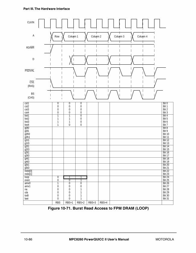
Part III. The Hardware Interface
Figure 10-71. Burst Read Access to FPM DRAM (LOOP)
cst1 0 0 0 Bit 0cst2 0 0 0 Bit 1cst3 0 0 0 Bit 2cst4 0 0 0 Bit 3bst1 1 1 0 Bit 4bst2 1 1 0 Bit 5bst3 1 1 0 Bit 6bst4 1 0 0 Bit 7g0l0 Bit 8g0l1 Bit 9g0h0 Bit 10g0h1 Bit 11g1t1 Bit 12g1t3 Bit 13g2t1 Bit 14g2t3 Bit 15g3t1 Bit 16g3t3 Bit 17g4t1 Bit 18g4t3 Bit 19g5t1 Bit 20g5t3 Bit 21redo[0] Bit 22redo[1] Bit 23loop 0 1 1 Bit 24exen 0 0 1 Bit 25amx0 1 0 0 Bit 26amx1 0 0 0 Bit 27na 0 0 1 Bit 28uta 0 0 1 Bit 29todt 0 0 1 Bit 30last 0 0 1 Bit 31
RBS RBS+1 RBS+2 RBS+3 RBS+4
CLKIN
A
RD/WR
D
PSDVAL
CS1
BS
Row Column 1 Column 2 Column 3 Column 4
(CAS)
(RAS)
10-86 MPC8260 PowerQUICC II UserÕs Manual MOTOROLA
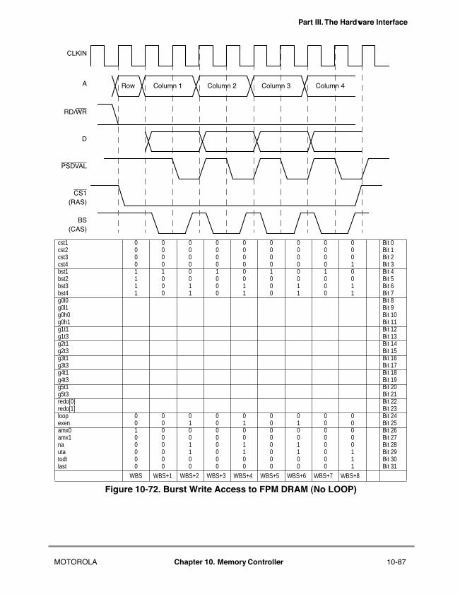
Part III. The Hardware Interface
Figure 10-72. Burst Write Access to FPM DRAM (No LOOP)
cst1 0 0 0 0 0 0 0 0 0 Bit 0cst2 0 0 0 0 0 0 0 0 0 Bit 1cst3 0 0 0 0 0 0 0 0 0 Bit 2cst4 0 0 0 0 0 0 0 0 1 Bit 3bst1 1 1 0 1 0 1 0 1 0 Bit 4bst2 1 0 0 0 0 0 0 0 0 Bit 5bst3 1 0 1 0 1 0 1 0 1 Bit 6bst4 1 0 1 0 1 0 1 0 1 Bit 7g0l0 Bit 8g0l1 Bit 9g0h0 Bit 10g0h1 Bit 11g1t1 Bit 12g1t3 Bit 13g2t1 Bit 14g2t3 Bit 15g3t1 Bit 16g3t3 Bit 17g4t1 Bit 18g4t3 Bit 19g5t1 Bit 20g5t3 Bit 21redo[0] Bit 22redo[1] Bit 23loop 0 0 0 0 0 0 0 0 0 Bit 24exen 0 0 1 0 1 0 1 0 0 Bit 25amx0 1 0 0 0 0 0 0 0 0 Bit 26amx1 0 0 0 0 0 0 0 0 0 Bit 27na 0 0 1 0 1 0 1 0 0 Bit 28uta 0 0 1 0 1 0 1 0 1 Bit 29todt 0 0 0 0 0 0 0 0 1 Bit 30last 0 0 0 0 0 0 0 0 1 Bit 31
WBS WBS+1 WBS+2 WBS+3 WBS+4 WBS+5 WBS+6 WBS+7 WBS+8
CLKIN
A
RD/WR
D
PSDVAL
CS1
BS
Row Column 1 Column 2 Column 3 Column 4
(RAS)
(CAS)
MOTOROLA Chapter 10. Memory Controller 10-87
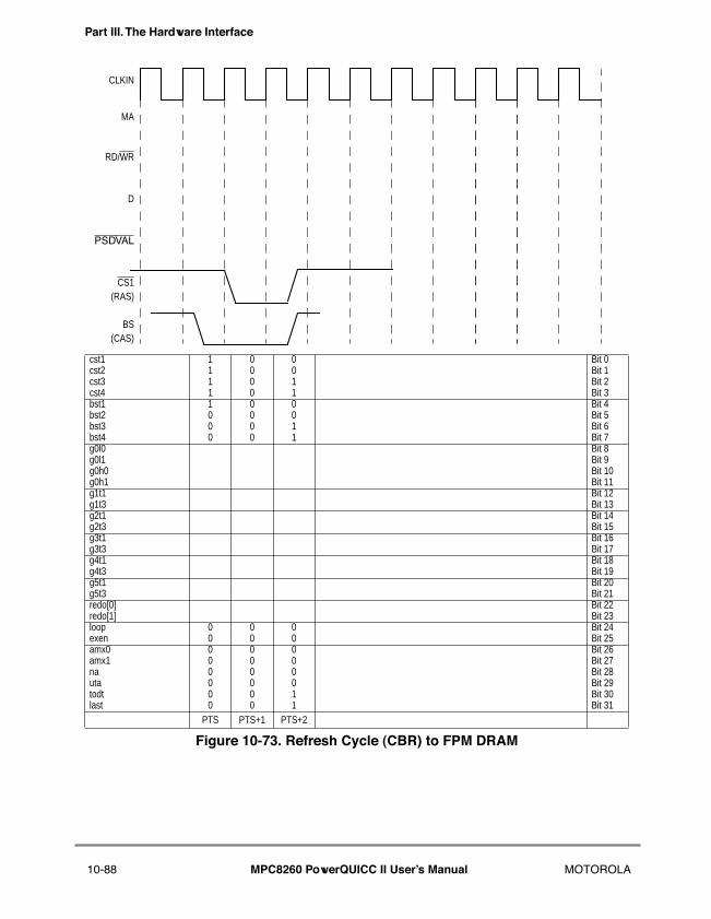
Part III. The Hardware Interface
Figure 10-73. Refresh Cycle (CBR) to FPM DRAM
cst1 1 0 0 Bit 0cst2 1 0 0 Bit 1cst3 1 0 1 Bit 2cst4 1 0 1 Bit 3bst1 1 0 0 Bit 4bst2 0 0 0 Bit 5bst3 0 0 1 Bit 6bst4 0 0 1 Bit 7g0l0 Bit 8g0l1 Bit 9g0h0 Bit 10g0h1 Bit 11g1t1 Bit 12g1t3 Bit 13g2t1 Bit 14g2t3 Bit 15g3t1 Bit 16g3t3 Bit 17g4t1 Bit 18g4t3 Bit 19g5t1 Bit 20g5t3 Bit 21redo[0] Bit 22redo[1] Bit 23loop 0 0 0 Bit 24exen 0 0 0 Bit 25amx0 0 0 0 Bit 26amx1 0 0 0 Bit 27na 0 0 0 Bit 28uta 0 0 0 Bit 29todt 0 0 1 Bit 30last 0 0 1 Bit 31
PTS PTS+1 PTS+2
CLKIN
MA
RD/WR
D
PSDVAL
CS1
BS(CAS)
(RAS)
10-88 MPC8260 PowerQUICC II UserÕs Manual MOTOROLA
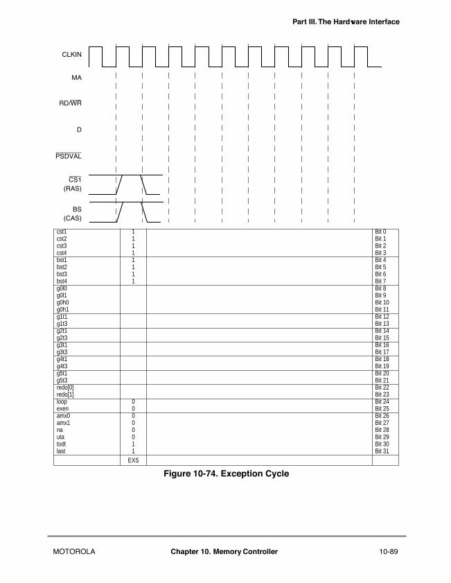
Part III. The Hardware Interface
Figure 10-74. Exception Cycle
cst1 1 Bit 0cst2 1 Bit 1cst3 1 Bit 2cst4 1 Bit 3bst1 1 Bit 4bst2 1 Bit 5bst3 1 Bit 6bst4 1 Bit 7g0l0 Bit 8g0l1 Bit 9g0h0 Bit 10g0h1 Bit 11g1t1 Bit 12g1t3 Bit 13g2t1 Bit 14g2t3 Bit 15g3t1 Bit 16g3t3 Bit 17g4t1 Bit 18g4t3 Bit 19g5t1 Bit 20g5t3 Bit 21redo[0] Bit 22redo[1] Bit 23loop 0 Bit 24exen 0 Bit 25amx0 0 Bit 26amx1 0 Bit 27na 0 Bit 28uta 0 Bit 29todt 1 Bit 30last 1 Bit 31
EXS
CLKIN
MA
RD/WR
D
PSDVAL
CS1
BS(CAS)
(RAS)
MOTOROLA Chapter 10. Memory Controller 10-89
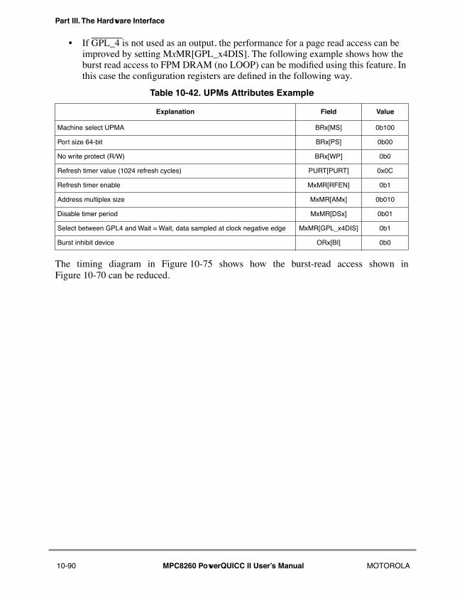
Part III. The Hardware Interface
¥ If GPL_4 is not used as an output, the performance for a page read access can be improved by setting MxMR[GPL_x4DIS]. The following example shows how the burst read access to FPM DRAM (no LOOP) can be modiÞed using this feature. In this case the conÞguration registers are deÞned in the following way.
The timing diagram in Figure 10-75 shows how the burst-read access shown inFigure 10-70 can be reduced.
Table 10-42. UPMs Attributes Example
Explanation Field Value
Machine select UPMA BRx[MS] 0b100
Port size 64-bit BRx[PS] 0b00
No write protect (R/W) BRx[WP] 0b0
Refresh timer value (1024 refresh cycles) PURT[PURT] 0x0C
Refresh timer enable MxMR[RFEN] 0b1
Address multiplex size MxMR[AMx] 0b010
Disable timer period MxMR[DSx] 0b01
Select between GPL4 and Wait = Wait, data sampled at clock negative edge MxMR[GPL_x4DIS] 0b1
Burst inhibit device ORx[BI] 0b0
10-90 MPC8260 PowerQUICC II UserÕs Manual MOTOROLA
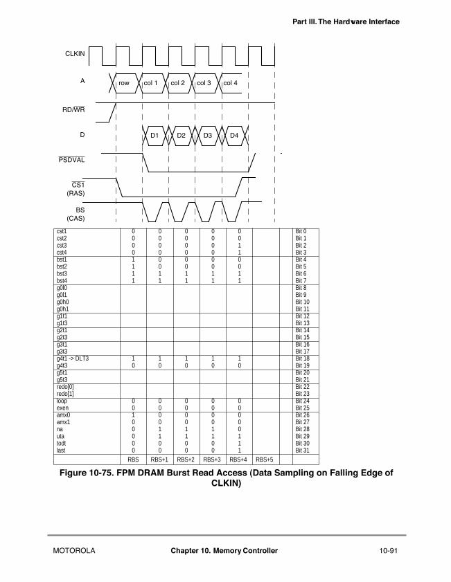
Part III. The Hardware Interface
Figure 10-75. FPM DRAM Burst Read Access (Data Sampling on Falling Edge of CLKIN)
cst1 0 0 0 0 0 Bit 0cst2 0 0 0 0 0 Bit 1cst3 0 0 0 0 1 Bit 2cst4 0 0 0 0 1 Bit 3bst1 1 0 0 0 0 Bit 4bst2 1 0 0 0 0 Bit 5bst3 1 1 1 1 1 Bit 6bst4 1 1 1 1 1 Bit 7g0l0 Bit 8g0l1 Bit 9g0h0 Bit 10g0h1 Bit 11g1t1 Bit 12g1t3 Bit 13g2t1 Bit 14g2t3 Bit 15g3t1 Bit 16g3t3 Bit 17g4t1 -> DLT3 1 1 1 1 1 Bit 18g4t3 0 0 0 0 0 Bit 19g5t1 Bit 20g5t3 Bit 21redo[0] Bit 22redo[1] Bit 23loop 0 0 0 0 0 Bit 24exen 0 0 0 0 0 Bit 25amx0 1 0 0 0 0 Bit 26amx1 0 0 0 0 0 Bit 27na 0 1 1 1 0 Bit 28uta 0 1 1 1 1 Bit 29todt 0 0 0 0 1 Bit 30last 0 0 0 0 1 Bit 31
RBS RBS+1 RBS+2 RBS+3 RBS+4 RBS+5
CLKIN
A
RD/WR
D
PSDVAL
CS1
BS
row col 1
(CAS)
(RAS)
col 2 col 3 col 4
D1 D2 D3 D4
MOTOROLA Chapter 10. Memory Controller 10-91
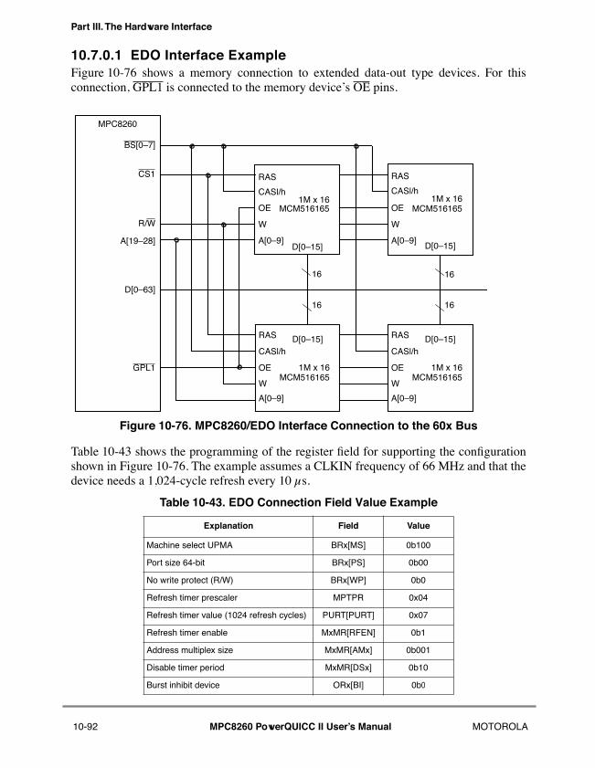
Part III. The Hardware Interface
10.7.0.1 EDO Interface ExampleFigure 10-76 shows a memory connection to extended data-out type devices. For thisconnection, GPL1 is connected to the memory deviceÕs OE pins.
Figure 10-76. MPC8260/EDO Interface Connection to the 60x Bus
Table 10-43 shows the programming of the register Þeld for supporting the conÞgurationshown in Figure 10-76. The example assumes a CLKIN frequency of 66 MHz and that thedevice needs a 1,024-cycle refresh every 10 µs.
Table 10-43. EDO Connection Field Value Example
Explanation Field Value
Machine select UPMA BRx[MS] 0b100
Port size 64-bit BRx[PS] 0b00
No write protect (R/W) BRx[WP] 0b0
Refresh timer prescaler MPTPR 0x04
Refresh timer value (1024 refresh cycles) PURT[PURT] 0x07
Refresh timer enable MxMR[RFEN] 0b1
Address multiplex size MxMR[AMx] 0b001
Disable timer period MxMR[DSx] 0b10
Burst inhibit device ORx[BI] 0b0
RAS
CASl/h
W
MCM5161651M x 16
16
A[0Ð9]D[0Ð15]
16
MPC8260
BS[0Ð7]
CS1
R/W
A[19Ð28]
D[0Ð63]
16
16
OE
RAS
CASl/h
W
MCM5161651M x 16
A[0Ð9]D[0Ð15]
OE
RAS
CASl/h
WMCM516165
1M x 16
A[0Ð9]
D[0Ð15]
OE
RAS
CASl/h
WMCM516165
1M x 16
A[0Ð9]
D[0Ð15]
OEGPL1
10-92 MPC8260 PowerQUICC II UserÕs Manual MOTOROLA
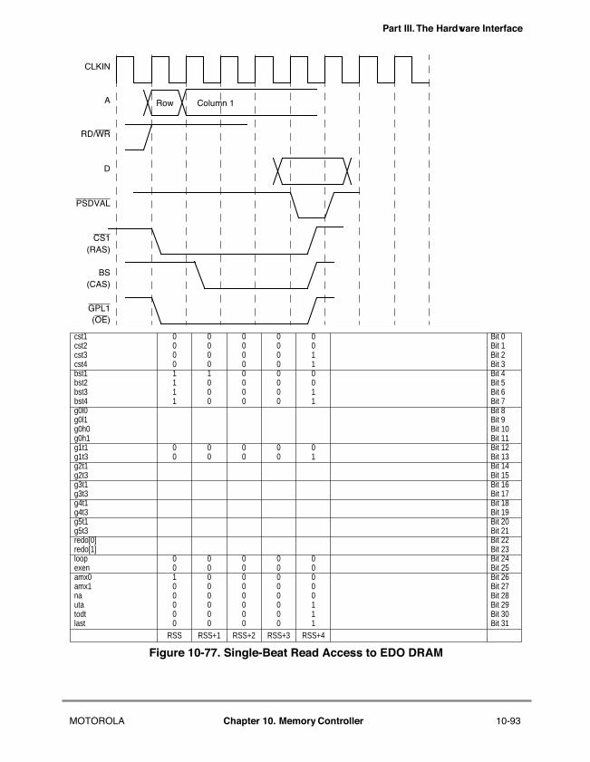
Part III. The Hardware Interface
Figure 10-77. Single-Beat Read Access to EDO DRAM
cst1 0 0 0 0 0 Bit 0cst2 0 0 0 0 0 Bit 1cst3 0 0 0 0 1 Bit 2cst4 0 0 0 0 1 Bit 3bst1 1 1 0 0 0 Bit 4bst2 1 0 0 0 0 Bit 5bst3 1 0 0 0 1 Bit 6bst4 1 0 0 0 1 Bit 7g0l0 Bit 8g0l1 Bit 9g0h0 Bit 10g0h1 Bit 11g1t1 0 0 0 0 0 Bit 12g1t3 0 0 0 0 1 Bit 13g2t1 Bit 14g2t3 Bit 15g3t1 Bit 16g3t3 Bit 17g4t1 Bit 18g4t3 Bit 19g5t1 Bit 20g5t3 Bit 21redo[0] Bit 22redo[1] Bit 23loop 0 0 0 0 0 Bit 24exen 0 0 0 0 0 Bit 25amx0 1 0 0 0 0 Bit 26amx1 0 0 0 0 0 Bit 27na 0 0 0 0 0 Bit 28uta 0 0 0 0 1 Bit 29todt 0 0 0 0 1 Bit 30last 0 0 0 0 1 Bit 31
RSS RSS+1 RSS+2 RSS+3 RSS+4
CLKIN
A
RD/WR
D
PSDVAL
CS1
BS
Row Column 1
(CAS)
(RAS)
GPL1(OE)
MOTOROLA Chapter 10. Memory Controller 10-93
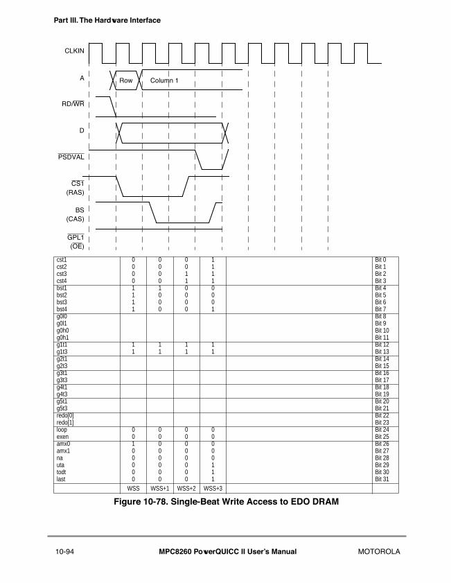
Part III. The Hardware Interface
Figure 10-78. Single-Beat Write Access to EDO DRAM
cst1 0 0 0 1 Bit 0cst2 0 0 0 1 Bit 1cst3 0 0 1 1 Bit 2cst4 0 0 1 1 Bit 3bst1 1 1 0 0 Bit 4bst2 1 0 0 0 Bit 5bst3 1 0 0 0 Bit 6bst4 1 0 0 1 Bit 7g0l0 Bit 8g0l1 Bit 9g0h0 Bit 10g0h1 Bit 11g1t1 1 1 1 1 Bit 12g1t3 1 1 1 1 Bit 13g2t1 Bit 14g2t3 Bit 15g3t1 Bit 16g3t3 Bit 17g4t1 Bit 18g4t3 Bit 19g5t1 Bit 20g5t3 Bit 21redo[0] Bit 22redo[1] Bit 23loop 0 0 0 0 Bit 24exen 0 0 0 0 Bit 25amx0 1 0 0 0 Bit 26amx1 0 0 0 0 Bit 27na 0 0 0 0 Bit 28uta 0 0 0 1 Bit 29todt 0 0 0 1 Bit 30last 0 0 0 1 Bit 31
WSS WSS+1 WSS+2 WSS+3
CLKIN
A
RD/WR
D
PSDVAL
CS1
BS
Row Column 1
(CAS)
(RAS)
GPL1(OE)
10-94 MPC8260 PowerQUICC II UserÕs Manual MOTOROLA
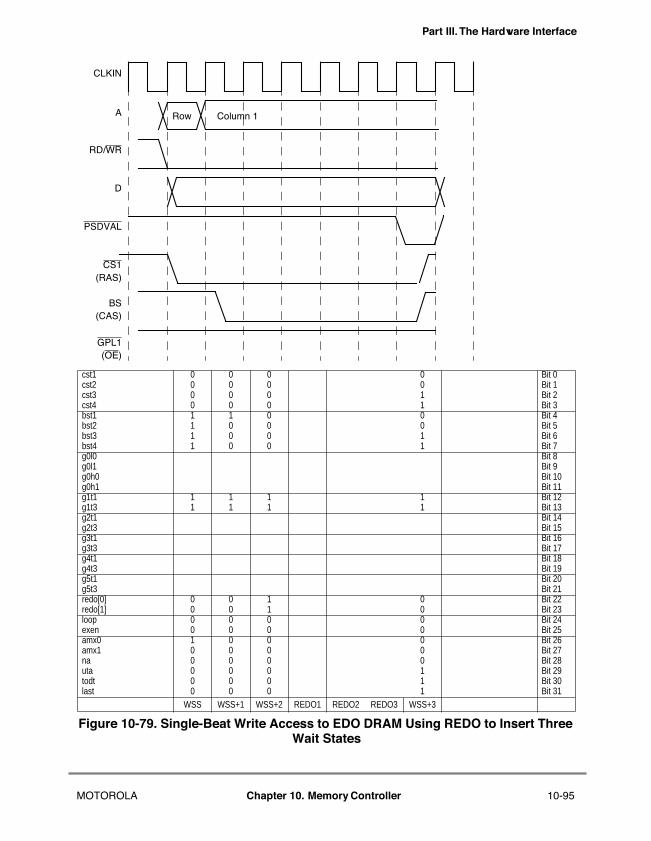
Part III. The Hardware Interface
Figure 10-79. Single-Beat Write Access to EDO DRAM Using REDO to Insert Three Wait States
cst1 0 0 0 0 Bit 0cst2 0 0 0 0 Bit 1cst3 0 0 0 1 Bit 2cst4 0 0 0 1 Bit 3bst1 1 1 0 0 Bit 4bst2 1 0 0 0 Bit 5bst3 1 0 0 1 Bit 6bst4 1 0 0 1 Bit 7g0l0 Bit 8g0l1 Bit 9g0h0 Bit 10g0h1 Bit 11g1t1 1 1 1 1 Bit 12g1t3 1 1 1 1 Bit 13g2t1 Bit 14g2t3 Bit 15g3t1 Bit 16g3t3 Bit 17g4t1 Bit 18g4t3 Bit 19g5t1 Bit 20g5t3 Bit 21redo[0] 0 0 1 0 Bit 22redo[1] 0 0 1 0 Bit 23loop 0 0 0 0 Bit 24exen 0 0 0 0 Bit 25amx0 1 0 0 0 Bit 26amx1 0 0 0 0 Bit 27na 0 0 0 0 Bit 28uta 0 0 0 1 Bit 29todt 0 0 0 1 Bit 30last 0 0 0 1 Bit 31
WSS WSS+1 WSS+2 REDO1 REDO2 REDO3 WSS+3
CLKIN
A
RD/WR
D
PSDVAL
CS1
BS
Row Column 1
(CAS)
(RAS)
GPL1(OE)
MOTOROLA Chapter 10. Memory Controller 10-95
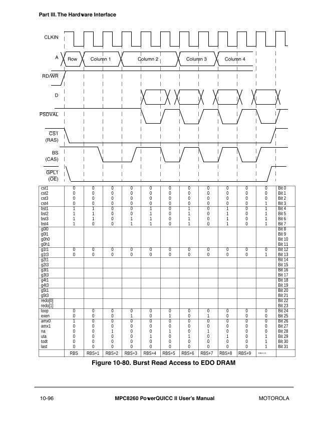
Part III. The Hardware Interface
Figure 10-80. Burst Read Access to EDO DRAM
cst1 0 0 0 0 0 0 0 0 0 0 0 Bit 0cst2 0 0 0 0 0 0 0 0 0 0 0 Bit 1cst3 0 0 0 0 0 0 0 0 0 0 0 Bit 2cst4 0 0 0 0 0 0 0 0 0 0 1 Bit 3bst1 1 1 0 0 1 0 1 0 1 0 1 Bit 4bst2 1 1 0 0 1 0 1 0 1 0 1 Bit 5bst3 1 1 0 1 1 0 1 0 1 0 1 Bit 6bst4 1 0 0 1 1 0 1 0 1 0 1 Bit 7g0l0 Bit 8g0l1 Bit 9g0h0 Bit 10g0h1 Bit 11g1t1 0 0 0 0 0 0 0 0 0 0 0 Bit 12g1t3 0 0 0 0 0 0 0 0 0 0 1 Bit 13g2t1 Bit 14g2t3 Bit 15g3t1 Bit 16g3t3 Bit 17g4t1 Bit 18g4t3 Bit 19g5t1 Bit 20g5t3 Bit 21redo[0] Bit 22redo[1] Bit 23loop 0 0 0 0 0 0 0 0 0 0 0 Bit 24exen 0 0 0 1 0 1 0 1 0 0 0 Bit 25amx0 1 0 0 0 0 0 0 0 0 0 0 Bit 26amx1 0 0 0 0 0 0 0 0 0 0 0 Bit 27na 0 0 1 0 0 1 0 1 0 0 0 Bit 28uta 0 0 0 0 1 0 1 0 1 0 1 Bit 29todt 0 0 0 0 0 0 0 0 0 0 1 Bit 30last 0 0 0 0 0 0 0 0 0 0 1 Bit 31
RBS RBS+1 RBS+2 RBS+3 RBS+4 RBS+5 RBS+6 RBS+7 RBS+8 RBS+9 RBS+10
CLKIN
A
RD/WR
D
PSDVAL
CS1
BS
Row Column 1
(CAS)
(RAS)
GPL1(OE)
Column 2 Column 3 Column 4
10-96 MPC8260 PowerQUICC II UserÕs Manual MOTOROLA
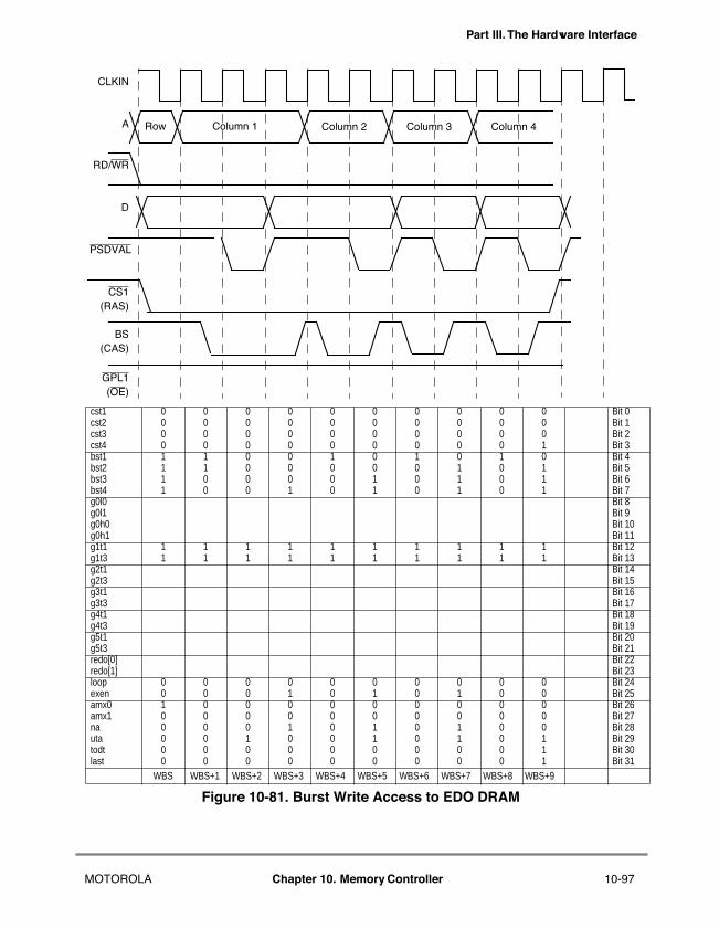
Part III. The Hardware Interface
Figure 10-81. Burst Write Access to EDO DRAM
cst1 0 0 0 0 0 0 0 0 0 0 Bit 0cst2 0 0 0 0 0 0 0 0 0 0 Bit 1cst3 0 0 0 0 0 0 0 0 0 0 Bit 2cst4 0 0 0 0 0 0 0 0 0 1 Bit 3bst1 1 1 0 0 1 0 1 0 1 0 Bit 4bst2 1 1 0 0 0 0 0 1 0 1 Bit 5bst3 1 0 0 0 0 1 0 1 0 1 Bit 6bst4 1 0 0 1 0 1 0 1 0 1 Bit 7g0l0 Bit 8g0l1 Bit 9g0h0 Bit 10g0h1 Bit 11g1t1 1 1 1 1 1 1 1 1 1 1 Bit 12g1t3 1 1 1 1 1 1 1 1 1 1 Bit 13g2t1 Bit 14g2t3 Bit 15g3t1 Bit 16g3t3 Bit 17g4t1 Bit 18g4t3 Bit 19g5t1 Bit 20g5t3 Bit 21redo[0] Bit 22redo[1] Bit 23loop 0 0 0 0 0 0 0 0 0 0 Bit 24exen 0 0 0 1 0 1 0 1 0 0 Bit 25amx0 1 0 0 0 0 0 0 0 0 0 Bit 26amx1 0 0 0 0 0 0 0 0 0 0 Bit 27na 0 0 0 1 0 1 0 1 0 0 Bit 28uta 0 0 1 0 0 1 0 1 0 1 Bit 29todt 0 0 0 0 0 0 0 0 0 1 Bit 30last 0 0 0 0 0 0 0 0 0 1 Bit 31
WBS WBS+1 WBS+2 WBS+3 WBS+4 WBS+5 WBS+6 WBS+7 WBS+8 WBS+9
CLKIN
A
RD/WR
D
PSDVAL
CS1
BS
Row Column 1
(CAS)
(RAS)
GPL1(OE)
Column 2 Column 3 Column 4
MOTOROLA Chapter 10. Memory Controller 10-97
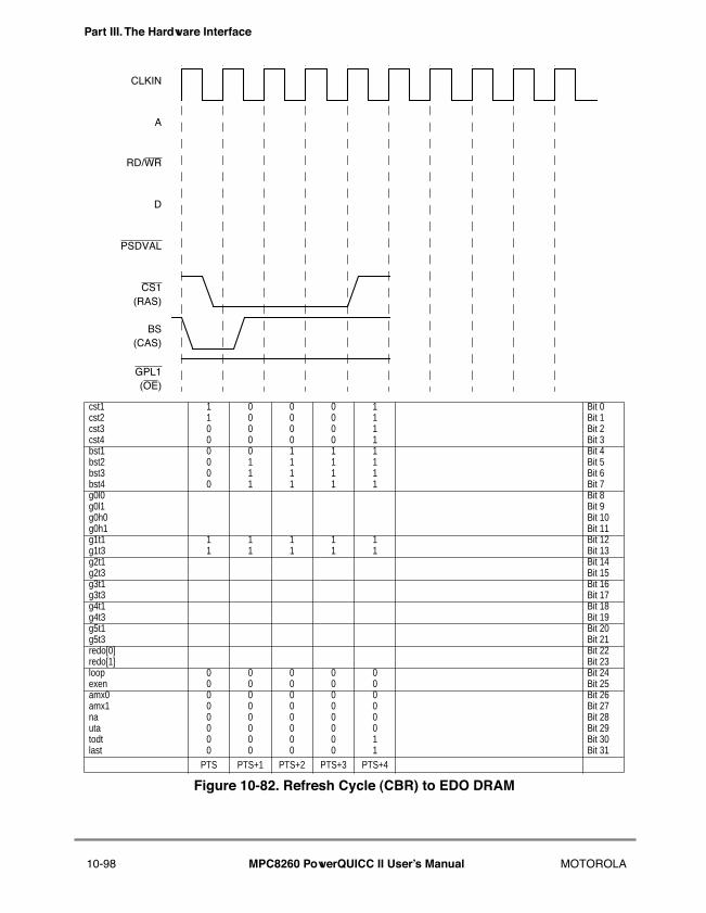
Part III. The Hardware Interface
Figure 10-82. Refresh Cycle (CBR) to EDO DRAM
cst1 1 0 0 0 1 Bit 0cst2 1 0 0 0 1 Bit 1cst3 0 0 0 0 1 Bit 2cst4 0 0 0 0 1 Bit 3bst1 0 0 1 1 1 Bit 4bst2 0 1 1 1 1 Bit 5bst3 0 1 1 1 1 Bit 6bst4 0 1 1 1 1 Bit 7g0l0 Bit 8g0l1 Bit 9g0h0 Bit 10g0h1 Bit 11g1t1 1 1 1 1 1 Bit 12g1t3 1 1 1 1 1 Bit 13g2t1 Bit 14g2t3 Bit 15g3t1 Bit 16g3t3 Bit 17g4t1 Bit 18g4t3 Bit 19g5t1 Bit 20g5t3 Bit 21redo[0] Bit 22redo[1] Bit 23loop 0 0 0 0 0 Bit 24exen 0 0 0 0 0 Bit 25amx0 0 0 0 0 0 Bit 26amx1 0 0 0 0 0 Bit 27na 0 0 0 0 0 Bit 28uta 0 0 0 0 0 Bit 29todt 0 0 0 0 1 Bit 30last 0 0 0 0 1 Bit 31
PTS PTS+1 PTS+2 PTS+3 PTS+4
CLKIN
A
RD/WR
D
PSDVAL
CS1
BS(CAS)
(RAS)
GPL1(OE)
10-98 MPC8260 PowerQUICC II UserÕs Manual MOTOROLA
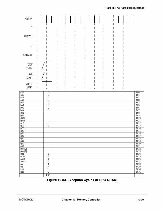
Part III. The Hardware Interface
Figure 10-83. Exception Cycle For EDO DRAM
cst1 1 Bit 0cst2 1 Bit 1cst3 1 Bit 2cst4 1 Bit 3bst1 1 Bit 4bst2 1 Bit 5bst3 1 Bit 6bst4 1 Bit 7g0l0 Bit 8g0l1 Bit 9g0h0 Bit 10g0h1 Bit 11g1t1 1 Bit 12g1t3 1 Bit 13g2t1 Bit 14g2t3 Bit 15g3t1 Bit 16g3t3 Bit 17g4t1 Bit 18g4t3 Bit 19g5t1 Bit 20g5t3 Bit 21redo[0] Bit 22redo[1] Bit 23loop 0 Bit 24exen 0 Bit 25amx0 0 Bit 26amx1 0 Bit 27na 0 Bit 28uta 0 Bit 29todt 1 Bit 30last 1 Bit 31
EXS
CLKIN
A
RD/WR
D
PSDVAL
CS1
BS(CAS)
(RAS)
GPL1(OE)
MOTOROLA Chapter 10. Memory Controller 10-99
Part III. The Hardware Interface
10.8 Handling Devices with Slow or Variable Access Times
The memory controller provides two ways to interface with slave devices that are very slow(access time is greater than the maximum allowed by the user programming model) orcannot guarantee a predeÞned access time (for example some FIFO, hierarchical businterface, or dual-port memory devices). These mechanisms are as follows:
¥ The wait mechanismÑUsed only in accesses controlled by the UPM. Setting MxMR[GPLx4DIS] enables this mechanism.
¥ The external termination (GTA) mechanism is used only in accesses controlled by the GPCM. ORx[SETA] speciÞes whether the access is terminated internally or externally.
The following examples show how the two mechanisms work.
10.8.1 Hierarchical Bus Interface ExampleAssume that the core initiates a local-bus read cycle that addresses main memory connectedto the system bus. The hierarchical bus interface accepts local bus requests and generates aread cycle on the system bus. The programmer cannot predict when valid data can belatched by the core because a DMA device may be occupying the system bus.
¥ The wait solution (UPM)ÑThe external module asserts UPWAIT to the memory controller to indicate that data is not ready. The memory controller synchronized this signal because the wait signal is asynchronous. As a result of the wait signal being asserted, the UPM enters a freeze mode at the rising edge of CLKIN upon encountering the WAEN bit being set in the UPM word. The UPM stays in that state until UPWAIT is negated. After UPWAIT is negated, the UPM continues executing from the next entry to the end of the pattern (LAST bit is set).
¥ The external termination solution (GPCM)ÑThe bus interface module asserts GTA to the memory controller when it can sample data. Note that GTA is also synchronized.
10.8.2 Slow Devices ExampleAssume that the core initiates a read cycle from a device whose access time exceeds themaximum allowed by the user programming model.
¥ The wait solution (UPM)ÑThe core generates a read access from the slow device. The device in turn asserts the wait signal until the data is ready. The core samples data only after the wait signal is negated.
¥ The external termination solution (GPCM)ÑThe core generates a read access from the slow device, which must generate the asynchronous GTA when it is ready.
10-100 MPC8260 PowerQUICC II UserÕs Manual MOTOROLA
Part III. The Hardware Interface
10.9 External Master Support (60x-Compatible Mode)The memory controller supports internal and external bus masters. Accesses from the coreor the CPM are considered internal; accesses from an external bus master are external.External bus master support is available only if the MPC8260 is placed in 60x-compatiblemode. This is done by setting the BCR[EBM], described in Section 4.3.2.1, ÒBusConÞguration Register (BCR).Ó
There are two types of external bus masters:
¥ Any 60x-compatible device that uses a 64-bit data bus, such as: MPC603e, MPC604e, MPC750, MPC2605 (L2 cache) in copy-back mode and others
¥ MPC8260 type devices
10.9.1 60x-Compatible External MastersAny 60x-compatible devices that use a 64-bit data bus can access the MPC8260 internalregisters and local bus. These devices can also use memory controller services under thefollowing restrictions, which apply only to 60x-assigned memory banks accessed by theexternal device:
¥ 64-bit port size only
¥ No ECC or RMW-parity
For 60x bus compatibility, the following connections should be observed:
¥ MPC8260Õs TSIZ[1Ð3] should be connected to the external masterÕs TSIZ[0Ð2]
¥ MPC8260Õs TSIZ[0] should be pulled down
¥ MPC8260Õs PSDVAL should be pulled up
10.9.2 MPC8260-Type External MastersAn MPC8260 external master is a 60x-compatible master with additional functionality. Asdescribed in the following, it has fewer the restrictions than other 60x-compatible masters:
¥ Any port size is allowed
¥ ECC and RMW-parity are supported
10.9.3 Extended Controls in 60x-Compatible ModeIn 60x-compatible mode, the memory controller provided extended controls for the gluelogic. The extended control consists of the following:
¥ Memory address latch (ALE) to latch the 60x address for memory use
¥ The address multiplex pin (GPL5/SDAMUX), which controls external multiplexing for DRAM and SDRAM devices
¥ LSB address pins (BADDR[27Ð31]) for incrementing memory addresses
MOTOROLA Chapter 10. Memory Controller 10-101
Part III. The Hardware Interface
¥ PSDVAL as a termination to a partial transaction (such as port-size beat access).
¥ Internal SDRAM bank selects (BNKSEL[0Ð2]) to allow SDRAM bank interleaving, as described in Section 10.9.4, ÒUsing BNKSEL SIgnals in Single-MPC8260 Bus Mode.Ó
10.9.4 Using BNKSEL SIgnals in Single-MPC8260 Bus ModeThe BNKSEL signals provide the following functionality in single-MPC8260 bus mode
¥ If bank-based interleaving is used, BNKSEL signals facilitate compatibility with SDRAMs that have different numbers of row or column address lines. The address lines of the MPC8260 bus and the BNKSEL lines can be routed independently to the address lines and BA lines of the DIMM. Note that all SDRAMs populated on an MPC8260 bus must still have the same organization. This ßexibility merely allows the SDRAMs to be populated as a group with larger or smaller devices as appropriate.
If BNKSEL lines were not used, the number of row and column address lines of the SDRAMs would affect which MPC8260 address bus lines on which the bank select signals would be driven, and would thus require that the BA signals of the SDRAMs be routed to those address lines, thus limiting ßexibility.
¥ If BCR[HP] is programmed, BNKSEL signals facilitate logic analysis of the system. Otherwise, the logic analyzer equipment must understand the address multiplexing scheme of the board and intelligently reconstruct the address of bus transactions.
10.9.5 Address Incrementing for External Bursting MastersBADDR[27Ð31] should be used to generate addresses to memory devices for burstaccesses. In 60x-compatible mode, when a master initiates an external bus transaction, itreßects the value of A[27Ð31] on the Þrst clock cycle of the memory access. These signalsare latched by the memory controller and on subsequent clock cycles, BADDR[27Ð31]increments as programmed in the UPM or after each data beat is sampled in the GPCM orafter each READ/WRITE command in the SDRAM machine (the SDRAM machine usesBADDR only for port sizes of 16 or 8 bits).
10.9.6 External Masters TimingExternal and internal masters have similar memory access timings. However, because ittakes more time to decode the addresses of external masters, memory accesses by externalmasters start one cycle later than those of internal masters.
As soon as the external master asserts TS, the memory controller compares the address witheach of its deÞned valid banks. If a match is found, the memory controller asserts theaddress latch enable (ALE) and control signals to the memory devices. The memorycontroller asserts PSDVAL for each data beat to indicate data beat termination on writetransactions and data valid on read transactions.
10-102 MPC8260 PowerQUICC II UserÕs Manual MOTOROLA
Part III. The Hardware Interface
The 60x bus is pipelined. The ALE pins control the external latch that latches the addressfrom the 60x bus and keeps the address stable for the memory access. The memorycontroller asserts ALE only on the start of new memory controller access.
Figure 10-84 shows the pipelined bus operation in 60x-compatible mode.
Figure 10-84. Pipelined Bus Operation and Memory Access in 60x-Compatible Mode
CLKIN
ADDR + ATTR
TS
AACK
DBG
PSDVAL
D
TA
CS
WE
OE
BADDR[27–28]
ALE
MA
00 01 02 03
MOTOROLA Chapter 10. Memory Controller 10-103
Part III. The Hardware Interface
Figure 10-85 shows the 1-cycle delay for external master access. For systems that use the60x bus with low frequency (33 MHz), the 1-cycle delay for external masters can beeliminated by setting BCR[EXDD].
Figure 10-85. External Master Access (GPCM)
10.9.6.1 Example of External Master Using the SDRAM MachineFigure 10-86 shows an interconnection in which a 60x-compatible external master and theMPC8260 can share access to a SDRAM bank. Note that the address multiplexer iscontrolled by SDAMUX, while the address latch is controlled by ALE. Also note thatbecause this is a 64-bit port size SDRAM, BADDR is not needed.
CLKIN
A[0–28]
A[27–31]
TT
TBST
TSIZ
TS
TA
CS
WE
OE
Data
AddressMatch andCompare
MemoryDeviceAccess
10-104 MPC8260 PowerQUICC II UserÕs Manual MOTOROLA
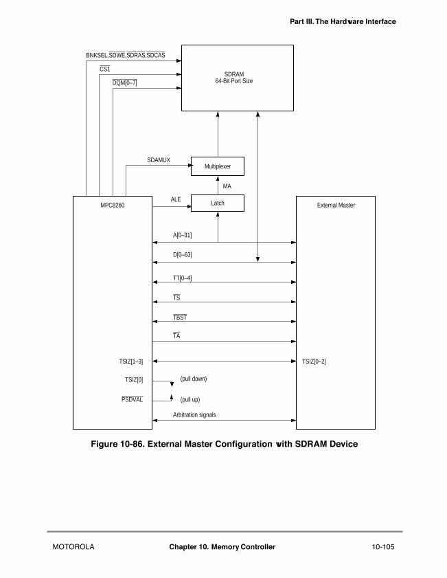
Part III. The Hardware Interface
Figure 10-86. External Master Configuration with SDRAM Device
SDAMUX
TT[0–4]
A[0–31]
DQM[0–7]
CS1
TS
TBST
TA
Arbitration signals
D[0–63]
SDRAM
Multiplexer
MPC8260 External MasterLatch
MA
ALE
BNKSEL,SDWE,SDRAS,SDCAS
64-Bit Port Size
TSIZ[1–3] TSIZ[0–2]
(pull down)
(pull up)
TSIZ[0]
PSDVAL
MOTOROLA Chapter 10. Memory Controller 10-105

Part III. The Hardware Interface
10-106 MPC8260 PowerQUICC II UserÕs Manual MOTOROLA
Chapter 11 Secondary (L2) Cache Support110110
The MPC8260 has features to support an externally controlled secondary (L2) cache suchas the Motorola MPC2605 integrated secondary cache for PowerPC microprocessors. Thischapter describes the MPC8260Õs L2 cache interfaceÑconÞgurations, operation,programmable parameters, system requirements, and timing.
11.1 L2 Cache ConÞgurationsThe MPC8260 supports three L2 cache conÞgurationsÑcopy-back mode, write-throughmode, and ECC/parity mode. The following sections describe the L2 cache modes.
11.1.1 Copy-Back ModeThe use of a copy-back L2 cache offers several advantages over direct access to the memorysystem. In copy-back mode, cacheable write operations are performed to the L2 cachewithout updating main memory. Since every cacheable write operation does not go to mainmemory but to the L2 cache which can be accessed more quickly, write operation latencyis reduced along with contention for the memory system. In copy-back mode, cacheableread operations that hit in the L2 cache are serviced from the L2 cache without requiring amemory transaction and its associated latency. Copy-back mode offers the greatestperformance of all the L2 cache modes.
Copy-back L2 cache blocks implement a dirty bit in their tag RAM, which indicateswhether the contents of the L2 cache block have been modiÞed from that in main memory.During L2 cache line replacement, L2 cache blocks that have been modiÞed (dirty) arewritten back to memory; unmodiÞed (not dirty) L2 cache blocks are invalidated andoverwritten without being written back to memory.
Copy-back mode requires that the L2 cache is able to initiate copy-backs to main memory.To do this, the L2 cache must act as a bus master and implement the bus arbitration signalsBR, BG, and DBG. The MPC8260 can also support additional bus masters (60x orMPC8260 type) in copy-back mode.
Figure 11-1 shows a MPC8260 connected to a MPC2605 integrated L2 cache in copy-backmode.
MOTOROLA Chapter 11. Secondary (L2) Cache Support 11-1
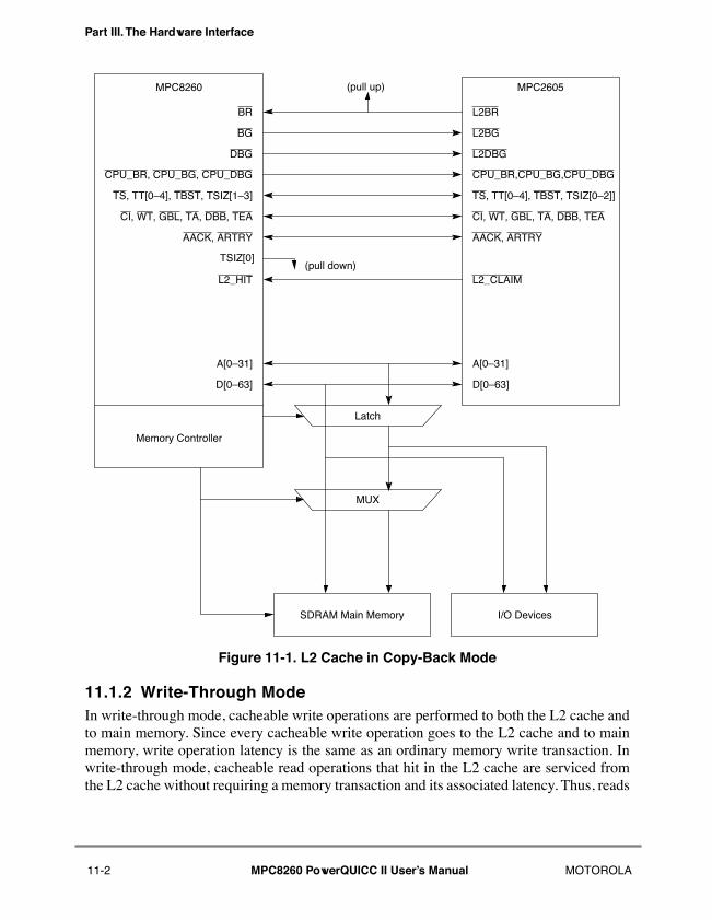
Part III. The Hardware Interface
Figure 11-1. L2 Cache in Copy-Back Mode
11.1.2 Write-Through ModeIn write-through mode, cacheable write operations are performed to both the L2 cache andto main memory. Since every cacheable write operation goes to the L2 cache and to mainmemory, write operation latency is the same as an ordinary memory write transaction. Inwrite-through mode, cacheable read operations that hit in the L2 cache are serviced fromthe L2 cache without requiring a memory transaction and its associated latency. Thus, reads
BR
DBG
TS, TT[0Ð4], TBST, TSIZ[1Ð3]
A[0Ð31]
CI, WT, GBL, TA, DBB, TEA
CPU_BR, CPU_BG, CPU_DBG
D[0Ð63]
MPC8260
L2BR
L2DBG
TS, TT[0Ð4], TBST, TSIZ[0Ð2]]
CI, WT, GBL, TA, DBB, TEA
AACK, ARTRY AACK, ARTRY
CPU_BR,CPU_BG,CPU_DBG
L2_CLAIML2_HIT
A[0Ð31]
D[0Ð63]
Memory Controller
SDRAM Main Memory
Latch
MUX
I/O Devices
MPC2605
BG L2BG
TSIZ[0](pull down)
(pull up)
11-2 MPC8260 PowerQUICC II UserÕs Manual MOTOROLA
Part III. The Hardware Interface
are serviced just as they are for copy-back mode. Write-through mode sacriÞces some ofthe write performance of copy-back mode, but guarantees L2 cache coherency with mainmemory.
Since write-through mode keeps memory coherent with the contents of the L2 cache, thereis never any need to perform an L2 copy-back. This removes the need for the L2 cache tomaintain a dirty bit in the tag RAM (all cache blocks are unmodiÞed) and it also removesthe need for bus arbitration signals.
The L2 cache is conÞgured for write-through mode by pulling down itÕs WT signal. Thereare no conÞguration changes to the MPC8260 required in write-through mode. TheMPC8260 can also support additional bus masters (60x or MPC8260 type) in write-throughmode.
Figure 11-2 shows a MPC8260 connected to a MPC2605 integrated L2 cache in write-through mode.
MOTOROLA Chapter 11. Secondary (L2) Cache Support 11-3
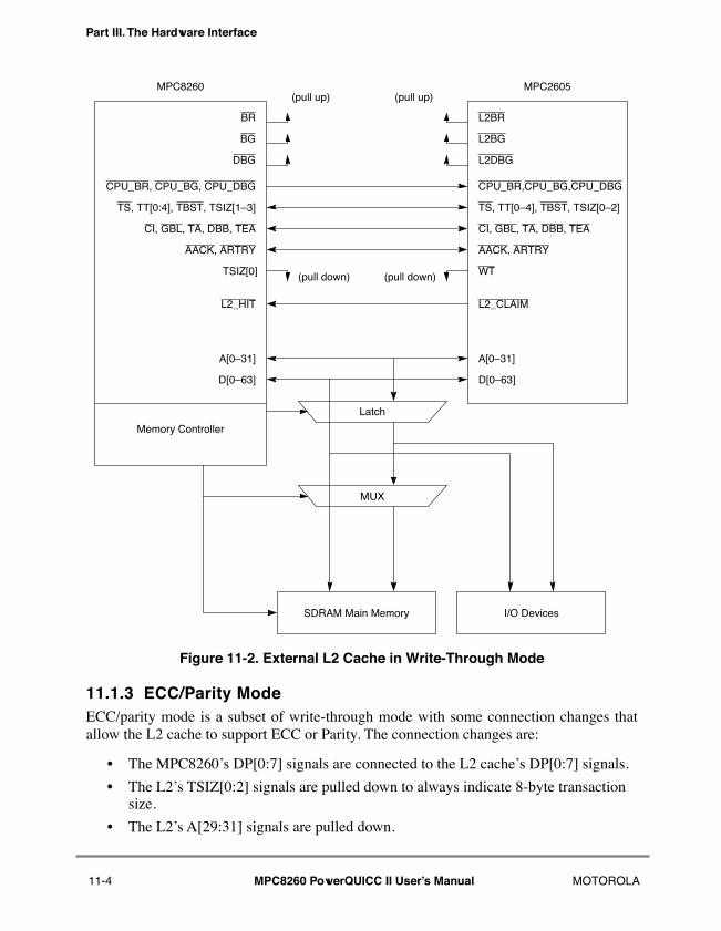
Part III. The Hardware Interface
Figure 11-2. External L2 Cache in Write-Through Mode
11.1.3 ECC/Parity ModeECC/parity mode is a subset of write-through mode with some connection changes thatallow the L2 cache to support ECC or Parity. The connection changes are:
¥ The MPC8260Õs DP[0:7] signals are connected to the L2 cacheÕs DP[0:7] signals.
¥ The L2Õs TSIZ[0:2] signals are pulled down to always indicate 8-byte transaction size.
¥ The L2Õs A[29:31] signals are pulled down.
BR
DBG
TS, TT[0:4], TBST, TSIZ[1Ð3]
A[0Ð31]
CI, GBL, TA, DBB, TEA
CPU_BR, CPU_BG, CPU_DBG
D[0Ð63]
MPC8260
L2BR
L2DBG
TS, TT[0Ð4], TBST, TSIZ[0Ð2]
CI, GBL, TA, DBB, TEA
AACK, ARTRY AACK, ARTRY
CPU_BR,CPU_BG,CPU_DBG
L2_CLAIML2_HIT
A[0Ð31]
D[0Ð63]
Memory Controller
SDRAM Main Memory
Latch
MUX
I/O Devices
MPC2605
BG L2BG
TSIZ[0] (pull down) WT(pull down)
(pull up)(pull up)
11-4 MPC8260 PowerQUICC II UserÕs Manual MOTOROLA
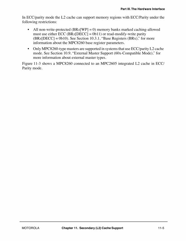
Part III. The Hardware Interface
In ECC/parity mode the L2 cache can support memory regions with ECC/Parity under thefollowing restrictions:
¥ All non-write-protected (BRx[WP] = 0) memory banks marked caching-allowed must use either ECC (BRx[DECC] = 0b11) or read-modify-write parity (BRx[DECC] = 0b10). See Section 10.3.1, ÒBase Registers (BRx),Ó for more information about the MPC8260 base register parameters.
¥ Only MPC8260-type masters are supported in systems that use ECC/parity L2 cache mode. See Section 10.9, ÒExternal Master Support (60x-Compatible Mode),Ó for more information about external master types.
Figure 11-3 shows a MPC8260 connected to an MPC2605 integrated L2 cache in ECC/Parity mode.
MOTOROLA Chapter 11. Secondary (L2) Cache Support 11-5
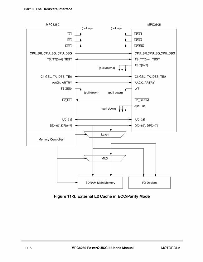
Part III. The Hardware Interface
Figure 11-3. External L2 Cache in ECC/Parity Mode
TS, TT[0Ð4], TBST
A[0Ð31]
CI, GBL, TA, DBB, TEA
CPU_BR, CPU_BG, CPU_DBG
D[0Ð63],DP[0Ð7]
MPC8260
TS, TT[0Ð4], TBST
CI, GBL, TA, DBB, TEA
AACK, ARTRY AACK, ARTRY
CPU_BR,CPU_BG,CPU_DBG
L2_CLAIML2_HIT
A[0Ð28]
D[0Ð63], DP[0Ð7]
Memory Controller
SDRAM Main Memory
Latch
MUX
I/O Devices
MPC2605
TSIZE[0](pull down)
WT(pull down)
TSIZ[0Ð2](pull downs)
A[29Ð31](pull downs)
BR
DBG
L2BR
L2DBG
BG L2BG
(pull up)(pull up)
11-6 MPC8260 PowerQUICC II UserÕs Manual MOTOROLA
Part III. The Hardware Interface
11.2 L2 Cache Interface ParametersThe L2 cache interface parameters in the bus conÞguration register (BCR) control theconÞguration and operation of the MPC8260Õs L2 interface. The parameters should beconÞgured as follows:
¥ BCR[EBM] = 1ÑMPC8260 in 60x-compatible mode.
¥ BCR[L2C] = 1ÑL2 cache is present.
¥ BCR[L2D] = 0ÑL2 response time. In this case, the L2 will claim a bus transaction one clock cycle after TS assertion.
¥ BCR[APD] = 1: This parameter is not L2 speciÞc, but should consider the L2 ARTRY assertion timing.
See Section 4.3.2.1, ÒBus ConÞguration Register (BCR),Ó for more details about theseparameters.
11.3 System Requirements When Using the L2 Cache InterfaceThe following requirements apply to MPC8260-based systems that implement an externalL2 cache:
¥ For systems that use copy-back mode, all cachable memory regions must be marked as global in the CPUÕs MMU and the CPMÕs RBA. This causes the assertion of the GBL signal on every cachable transaction. Systems that use write-through mode (or ECC/Parity mode) have no such restriction.
¥ All cachable memory regions must have a 64-bit port size.
¥ All cachable memory regions must not set the BRx[DR] bit.
¥ All cachable memory regions must not use ECC or parity unless the external L2 is connected as described in Section 11.1.3, ÒECC/Parity Mode.Ó
¥ All non-cachable memory regions must be marked as caching-inhibited in the CPUÕs MMU. This causes the assertion of the CI signal on every non-cachable transaction. Note that the MPC8260Õs internal space (IMMR) and any memory banks assigned to the local bus are always considered non-cachable.
11.4 L2 Cache OperationWhen conÞgured for an L2 cache (BCR[L2C] = 1), the MPC8260 samples the L2_HITinput signal when the delay time programmed in BCR[L2D] expires. For 60x bus cycles, ifL2_HIT is asserted, the external L2 cache drives AACK and TA to complete the transactionwithout the MPC8260 initiating a system memory transfer.
The external L2 cache can assert ARTRY to retry 60x bus cycles, and can request the busby asserting BR to perform L2 cast-out operations. The arbiter grants the address and data
MOTOROLA Chapter 11. Secondary (L2) Cache Support 11-7
Part III. The Hardware Interface
bus to the external L2 cache by asserting BG and DBG, respectively. If the external L2cache asserts ARTRY, it should not assert L2_HIT.
For more information about the timing and behavior of the MPC2605 integrated L2 cache,refer to the MPC2605 data sheet.
11.5 Timing ExampleFigure 11-4 shows a read access performed by the MPC8260 with an externally controlledL2 cache. For the Þrst transaction (A0), the MPC8260 grants the bus and asserts TS withthe address and address transfer attributes. In this example, BCR[L2D] = 0, which meansthat L2_HIT is valid one clock cycle after the assertion of TS. The MPC8260 samplesL2_HIT when L2D expires. In the second transaction (A1), the access misses in the L2cache and the memory controller starts the transaction a minimum of three cycles after theassertion of TS.
11-8 MPC8260 PowerQUICC II UserÕs Manual MOTOROLA
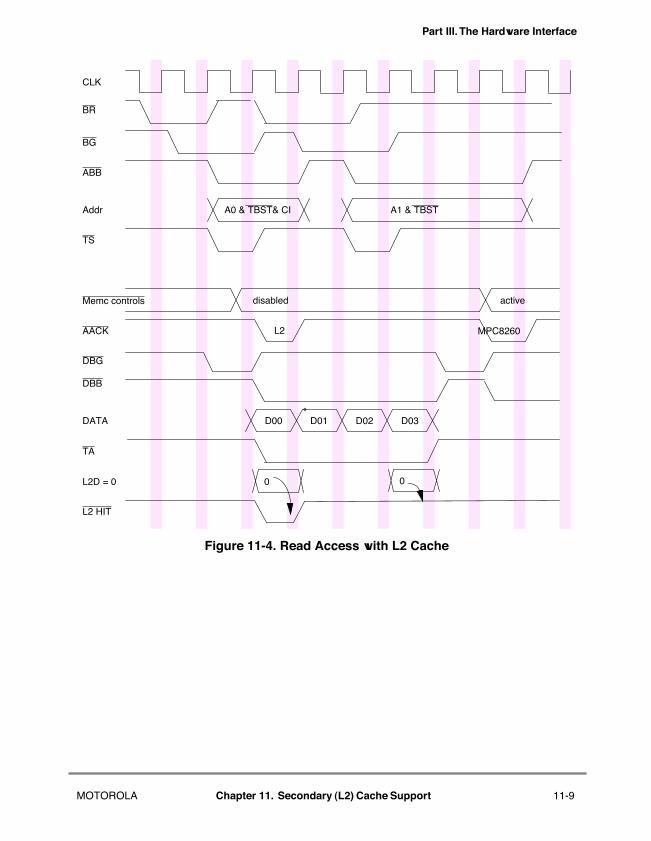
Part III. The Hardware Interface
Figure 11-4. Read Access with L2 Cache
CLK
BR
BG
Addr
TS
ABB
A0 & TBST& CI
Memc controls
AACK
DBG
DBB
DATA
TA
D00
active
A1 & TBST
D01 D02 D03
L2 HIT
L2D = 0 0
L2
disabled
MPC8260
0
MOTOROLA Chapter 11. Secondary (L2) Cache Support 11-9

Part III. The Hardware Interface
11-10 MPC8260 PowerQUICC II UserÕs Manual MOTOROLA
Chapter 12 IEEE 1149.1 Test Access Port120120
The MPC8260 provides a dedicated user-accessible test access port (TAP) that is fullycompatible with the IEEE 1149.1 Standard Test Access Port and Boundary ScanArchitecture. Problems associated with testing high-density circuit boards have led todevelopment of this proposed standard under the sponsorship of the Test TechnologyCommittee of IEEE and the Joint Test Action Group (JTAG). The MPC8260Õsimplementation supports circuit-board test strategies based on this standard.
The TAP consists of Þve dedicated signal pinsÑa 16-state TAP controller and two test dataregisters. A boundary scan register links all device signal pins into a single shift register.The test logic, which is implemented using static logic design, is independent of the devicesystem logic. The MPC8260Õs implementation provides the capability to do the following:
¥ Perform boundary scan operations to check circuit-board electrical continuity.
¥ Bypass the MPC8260 for a given circuit-board test by effectively reducing the boundary scan register to a single cell.
¥ Sample the MPC8260 system pins during operation and transparently shift out the result in the boundary-scan register.
¥ Disable the output drive to pins during circuit-board testing.
NOTEPrecautions must be observed to ensure that the IEEE 1149.1-like test logic does not interfere with nontest operation.
12.1 OverviewThe MPC8260Õs implementation includes a TAP controller, a 4-bit instruction register, andtwo test registers (a 1-bit bypass register and a 475-bit boundary scan register). Figure 12-1shows an overview of the MPC8260Õs scan chain implementation.
MOTOROLA Chapter 12. IEEE 1149.1 Test Access Port 12-1
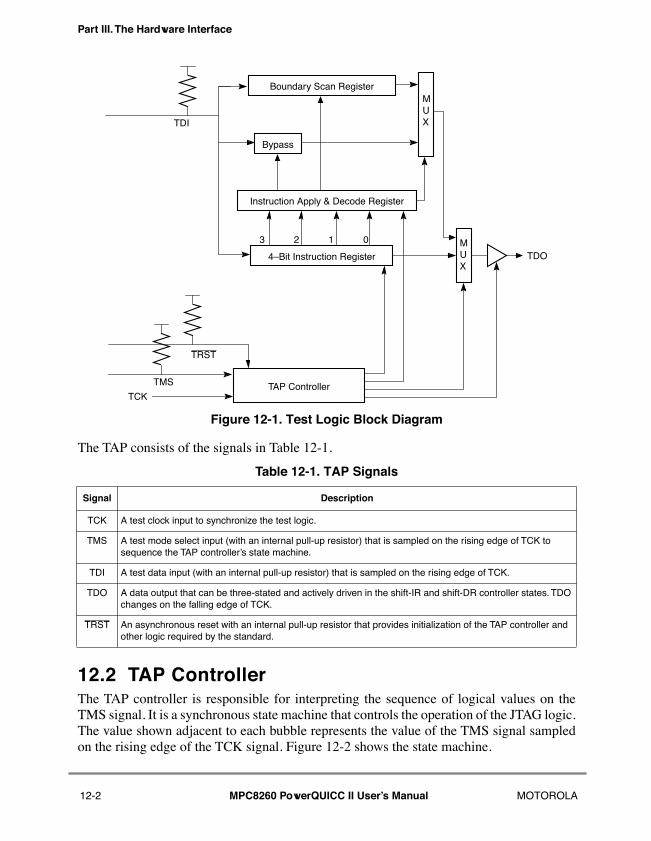
Part III. The Hardware Interface
Figure 12-1. Test Logic Block Diagram
The TAP consists of the signals in Table 12-1.
12.2 TAP ControllerThe TAP controller is responsible for interpreting the sequence of logical values on theTMS signal. It is a synchronous state machine that controls the operation of the JTAG logic.The value shown adjacent to each bubble represents the value of the TMS signal sampledon the rising edge of the TCK signal. Figure 12-2 shows the state machine.
Table 12-1. TAP Signals
Signal Description
TCK A test clock input to synchronize the test logic.
TMS A test mode select input (with an internal pull-up resistor) that is sampled on the rising edge of TCK to sequence the TAP controllerÕs state machine.
TDI A test data input (with an internal pull-up resistor) that is sampled on the rising edge of TCK.
TDO A data output that can be three-stated and actively driven in the shift-IR and shift-DR controller states. TDO changes on the falling edge of TCK.
TRST An asynchronous reset with an internal pull-up resistor that provides initialization of the TAP controller and other logic required by the standard.
Boundary Scan Register
Bypass
MUX
Instruction Apply & Decode Register
4ÐBit Instruction RegisterMUX
TDO
TDI
TMS
TCK
TRST
012
TAP Controller
3
12-2 MPC8260 PowerQUICC II UserÕs Manual MOTOROLA
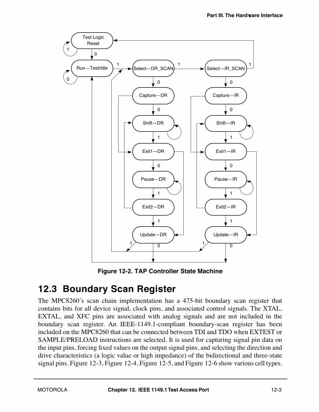
Part III. The Hardware Interface
Figure 12-2. TAP Controller State Machine
12.3 Boundary Scan RegisterThe MPC8260Õs scan chain implementation has a 475-bit boundary scan register thatcontains bits for all device signal, clock pins, and associated control signals. The XTAL,EXTAL, and XFC pins are associated with analog signals and are not included in theboundary scan register. An IEEE-1149.1-compliant boundary-scan register has beenincluded on the MPC8260 that can be connected between TDI and TDO when EXTEST orSAMPLE/PRELOAD instructions are selected. It is used for capturing signal pin data onthe input pins, forcing Þxed values on the output signal pins, and selecting the direction anddrive characteristics (a logic value or high impedance) of the bidirectional and three-statesignal pins. Figure 12-3, Figure 12-4, Figure 12-5, and Figure 12-6 show various cell types.
Test LogicReset
RunÑTest/Idle SelectÑDR_SCAN
CaptureÑDR
ShiftÑDR
Exit1ÑDR
PauseÑDR
Exit2ÑDR
UpdateÑDR
SelectÑIR_SCAN
CaptureÑIR
ShiftÑIR
Exit1ÑIR
PauseÑIR
Exit2ÑIR
UpdateÑIR
0 0
0
0
1
1
1
0 0
0
0
1
111
1
0
0
1
1
11
MOTOROLA Chapter 12. IEEE 1149.1 Test Access Port 12-3
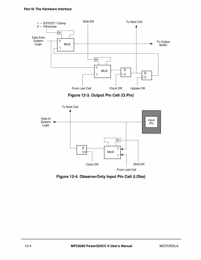
Part III. The Hardware Interface
Figure 12-3. Output Pin Cell (O.Pin)
Figure 12-4. Observe-Only Input Pin Cell (I.Obs)
1
1MUX
1
1MUX
G1
C
D
CD
From Last Cell Clock DR Update DR
Shift DR1 Ñ EXTEST | Clamp
Data fromTo Output
Buffer
0 Ñ Otherwise
LogicSystem
To Next Cell
G1
1
1MUX
G1
CD
From Last Cell
Clock DR
Data toSystemLogic
InputPin
Shift DR
To Next Cell
12-4 MPC8260 PowerQUICC II UserÕs Manual MOTOROLA
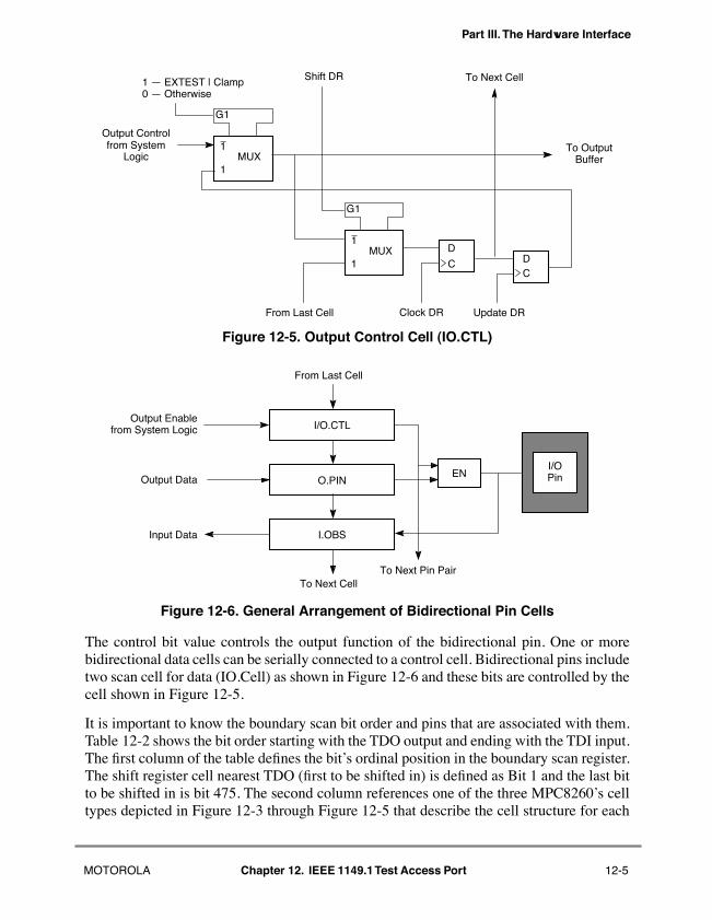
Part III. The Hardware Interface
Figure 12-5. Output Control Cell (IO.CTL)
Figure 12-6. General Arrangement of Bidirectional Pin Cells
The control bit value controls the output function of the bidirectional pin. One or morebidirectional data cells can be serially connected to a control cell. Bidirectional pins includetwo scan cell for data (IO.Cell) as shown in Figure 12-6 and these bits are controlled by thecell shown in Figure 12-5.
It is important to know the boundary scan bit order and pins that are associated with them.Table 12-2 shows the bit order starting with the TDO output and ending with the TDI input.The Þrst column of the table deÞnes the bitÕs ordinal position in the boundary scan register.The shift register cell nearest TDO (Þrst to be shifted in) is deÞned as Bit 1 and the last bitto be shifted in is bit 475. The second column references one of the three MPC8260Õs celltypes depicted in Figure 12-3 through Figure 12-5 that describe the cell structure for each
1
1MUX
G1
1
1MUX
G1
C
D
CD
From Last Cell Clock DR Update DR
Shift DR1 Ñ EXTEST | Clamp
To OutputBuffer
0 Ñ Otherwise
To Next Cell
Output Control
Logicfrom System
I/OPin
From Last Cell
Output Data
Input Data
Output Enable
I.OBS
EN
from System Logic
O.PIN
I/O.CTL
To Next Pin PairTo Next Cell
MOTOROLA Chapter 12. IEEE 1149.1 Test Access Port 12-5
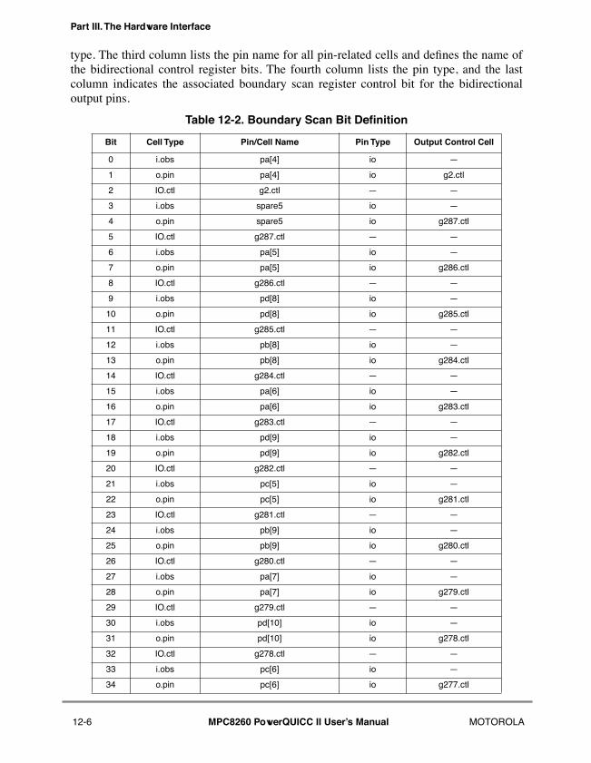
Part III. The Hardware Interface
type. The third column lists the pin name for all pin-related cells and deÞnes the name ofthe bidirectional control register bits. The fourth column lists the pin type, and the lastcolumn indicates the associated boundary scan register control bit for the bidirectionaloutput pins.
Table 12-2. Boundary Scan Bit Definition
Bit Cell Type Pin/Cell Name Pin Type Output Control Cell
0 i.obs pa[4] io Ñ
1 o.pin pa[4] io g2.ctl
2 IO.ctl g2.ctl Ñ Ñ
3 i.obs spare5 io Ñ
4 o.pin spare5 io g287.ctl
5 IO.ctl g287.ctl Ñ Ñ
6 i.obs pa[5] io Ñ
7 o.pin pa[5] io g286.ctl
8 IO.ctl g286.ctl Ñ Ñ
9 i.obs pd[8] io Ñ
10 o.pin pd[8] io g285.ctl
11 IO.ctl g285.ctl Ñ Ñ
12 i.obs pb[8] io Ñ
13 o.pin pb[8] io g284.ctl
14 IO.ctl g284.ctl Ñ Ñ
15 i.obs pa[6] io Ñ
16 o.pin pa[6] io g283.ctl
17 IO.ctl g283.ctl Ñ Ñ
18 i.obs pd[9] io Ñ
19 o.pin pd[9] io g282.ctl
20 IO.ctl g282.ctl Ñ Ñ
21 i.obs pc[5] io Ñ
22 o.pin pc[5] io g281.ctl
23 IO.ctl g281.ctl Ñ Ñ
24 i.obs pb[9] io Ñ
25 o.pin pb[9] io g280.ctl
26 IO.ctl g280.ctl Ñ Ñ
27 i.obs pa[7] io Ñ
28 o.pin pa[7] io g279.ctl
29 IO.ctl g279.ctl Ñ Ñ
30 i.obs pd[10] io Ñ
31 o.pin pd[10] io g278.ctl
32 IO.ctl g278.ctl Ñ Ñ
33 i.obs pc[6] io Ñ
34 o.pin pc[6] io g277.ctl
12-6 MPC8260 PowerQUICC II UserÕs Manual MOTOROLA
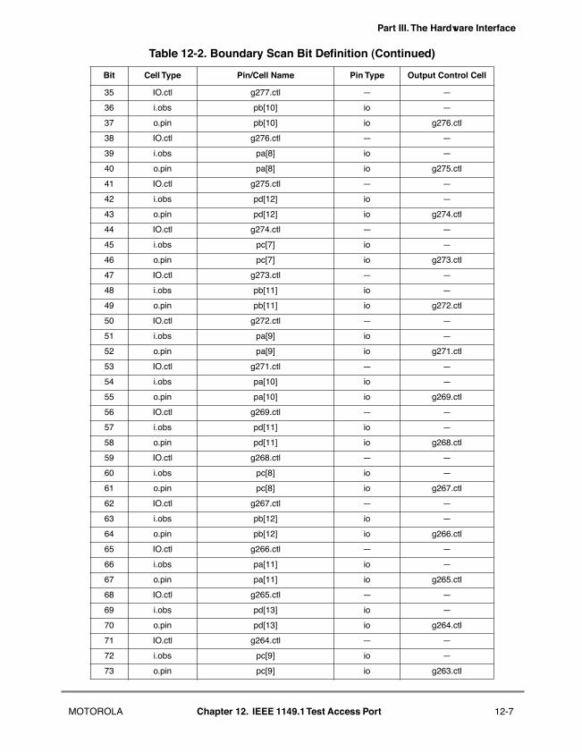
Part III. The Hardware Interface
35 IO.ctl g277.ctl Ñ Ñ
36 i.obs pb[10] io Ñ
37 o.pin pb[10] io g276.ctl
38 IO.ctl g276.ctl Ñ Ñ
39 i.obs pa[8] io Ñ
40 o.pin pa[8] io g275.ctl
41 IO.ctl g275.ctl Ñ Ñ
42 i.obs pd[12] io Ñ
43 o.pin pd[12] io g274.ctl
44 IO.ctl g274.ctl Ñ Ñ
45 i.obs pc[7] io Ñ
46 o.pin pc[7] io g273.ctl
47 IO.ctl g273.ctl Ñ Ñ
48 i.obs pb[11] io Ñ
49 o.pin pb[11] io g272.ctl
50 IO.ctl g272.ctl Ñ Ñ
51 i.obs pa[9] io Ñ
52 o.pin pa[9] io g271.ctl
53 IO.ctl g271.ctl Ñ Ñ
54 i.obs pa[10] io Ñ
55 o.pin pa[10] io g269.ctl
56 IO.ctl g269.ctl Ñ Ñ
57 i.obs pd[11] io Ñ
58 o.pin pd[11] io g268.ctl
59 IO.ctl g268.ctl Ñ Ñ
60 i.obs pc[8] io Ñ
61 o.pin pc[8] io g267.ctl
62 IO.ctl g267.ctl Ñ Ñ
63 i.obs pb[12] io Ñ
64 o.pin pb[12] io g266.ctl
65 IO.ctl g266.ctl Ñ Ñ
66 i.obs pa[11] io Ñ
67 o.pin pa[11] io g265.ctl
68 IO.ctl g265.ctl Ñ Ñ
69 i.obs pd[13] io Ñ
70 o.pin pd[13] io g264.ctl
71 IO.ctl g264.ctl Ñ Ñ
72 i.obs pc[9] io Ñ
73 o.pin pc[9] io g263.ctl
Table 12-2. Boundary Scan Bit Definition (Continued)
Bit Cell Type Pin/Cell Name Pin Type Output Control Cell
MOTOROLA Chapter 12. IEEE 1149.1 Test Access Port 12-7
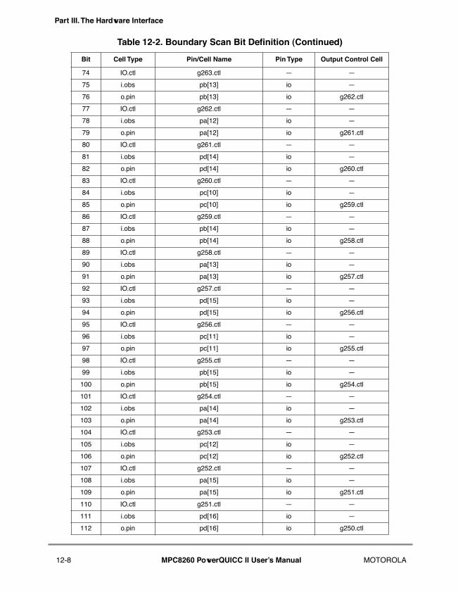
Part III. The Hardware Interface
74 IO.ctl g263.ctl Ñ Ñ
75 i.obs pb[13] io Ñ
76 o.pin pb[13] io g262.ctl
77 IO.ctl g262.ctl Ñ Ñ
78 i.obs pa[12] io Ñ
79 o.pin pa[12] io g261.ctl
80 IO.ctl g261.ctl Ñ Ñ
81 i.obs pd[14] io Ñ
82 o.pin pd[14] io g260.ctl
83 IO.ctl g260.ctl Ñ Ñ
84 i.obs pc[10] io Ñ
85 o.pin pc[10] io g259.ctl
86 IO.ctl g259.ctl Ñ Ñ
87 i.obs pb[14] io Ñ
88 o.pin pb[14] io g258.ctl
89 IO.ctl g258.ctl Ñ Ñ
90 i.obs pa[13] io Ñ
91 o.pin pa[13] io g257.ctl
92 IO.ctl g257.ctl Ñ Ñ
93 i.obs pd[15] io Ñ
94 o.pin pd[15] io g256.ctl
95 IO.ctl g256.ctl Ñ Ñ
96 i.obs pc[11] io Ñ
97 o.pin pc[11] io g255.ctl
98 IO.ctl g255.ctl Ñ Ñ
99 i.obs pb[15] io Ñ
100 o.pin pb[15] io g254.ctl
101 IO.ctl g254.ctl Ñ Ñ
102 i.obs pa[14] io Ñ
103 o.pin pa[14] io g253.ctl
104 IO.ctl g253.ctl Ñ Ñ
105 i.obs pc[12] io Ñ
106 o.pin pc[12] io g252.ctl
107 IO.ctl g252.ctl Ñ Ñ
108 i.obs pa[15] io Ñ
109 o.pin pa[15] io g251.ctl
110 IO.ctl g251.ctl Ñ Ñ
111 i.obs pd[16] io Ñ
112 o.pin pd[16] io g250.ctl
Table 12-2. Boundary Scan Bit Definition (Continued)
Bit Cell Type Pin/Cell Name Pin Type Output Control Cell
12-8 MPC8260 PowerQUICC II UserÕs Manual MOTOROLA
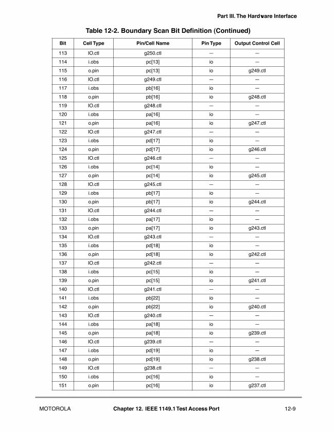
Part III. The Hardware Interface
113 IO.ctl g250.ctl Ñ Ñ
114 i.obs pc[13] io Ñ
115 o.pin pc[13] io g249.ctl
116 IO.ctl g249.ctl Ñ Ñ
117 i.obs pb[16] io Ñ
118 o.pin pb[16] io g248.ctl
119 IO.ctl g248.ctl Ñ Ñ
120 i.obs pa[16] io Ñ
121 o.pin pa[16] io g247.ctl
122 IO.ctl g247.ctl Ñ Ñ
123 i.obs pd[17] io Ñ
124 o.pin pd[17] io g246.ctl
125 IO.ctl g246.ctl Ñ Ñ
126 i.obs pc[14] io Ñ
127 o.pin pc[14] io g245.ctl
128 IO.ctl g245.ctl Ñ Ñ
129 i.obs pb[17] io Ñ
130 o.pin pb[17] io g244.ctl
131 IO.ctl g244.ctl Ñ Ñ
132 i.obs pa[17] io Ñ
133 o.pin pa[17] io g243.ctl
134 IO.ctl g243.ctl Ñ Ñ
135 i.obs pd[18] io Ñ
136 o.pin pd[18] io g242.ctl
137 IO.ctl g242.ctl Ñ Ñ
138 i.obs pc[15] io Ñ
139 o.pin pc[15] io g241.ctl
140 IO.ctl g241.ctl Ñ Ñ
141 i.obs pb[22] io Ñ
142 o.pin pb[22] io g240.ctl
143 IO.ctl g240.ctl Ñ Ñ
144 i.obs pa[18] io Ñ
145 o.pin pa[18] io g239.ctl
146 IO.ctl g239.ctl Ñ Ñ
147 i.obs pd[19] io Ñ
148 o.pin pd[19] io g238.ctl
149 IO.ctl g238.ctl Ñ Ñ
150 i.obs pc[16] io Ñ
151 o.pin pc[16] io g237.ctl
Table 12-2. Boundary Scan Bit Definition (Continued)
Bit Cell Type Pin/Cell Name Pin Type Output Control Cell
MOTOROLA Chapter 12. IEEE 1149.1 Test Access Port 12-9
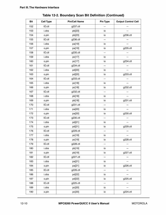
Part III. The Hardware Interface
152 IO.ctl g237.ctl Ñ Ñ
153 i.obs pb[23] io Ñ
154 o.pin pb[23] io g236.ctl
155 IO.ctl g236.ctl Ñ Ñ
156 i.obs pa[19] io Ñ
157 o.pin pa[19] io g235.ctl
158 IO.ctl g235.ctl Ñ Ñ
159 i.obs pc[17] io Ñ
160 o.pin pc[17] io g234.ctl
161 IO.ctl g234.ctl Ñ Ñ
162 i.obs pd[20] io Ñ
163 o.pin pd[20] io g233.ctl
164 IO.ctl g233.ctl Ñ Ñ
165 i.obs pc[18] io Ñ
166 o.pin pc[18] io g232.ctl
167 IO.ctl g232.ctl Ñ Ñ
168 i.obs pb[18] io Ñ
169 o.pin pb[18] io g231.ctl
170 IO.ctl g231.ctl Ñ Ñ
171 i.obs pa[20] io Ñ
172 o.pin pa[20] io g230.ctl
173 IO.ctl g230.ctl Ñ Ñ
174 i.obs pd[21] io Ñ
175 o.pin pd[21] io g229.ctl
176 IO.ctl g229.ctl Ñ Ñ
177 i.obs pc[19] io Ñ
178 o.pin pc[19] io g228.ctl
179 IO.ctl g228.ctl Ñ Ñ
180 i.obs pb[19] io Ñ
181 o.pin pb[19] io g227.ctl
182 IO.ctl g227.ctl Ñ Ñ
183 i.obs pa[21] io Ñ
184 o.pin pa[21] io g226.ctl
185 IO.ctl g226.ctl Ñ Ñ
186 i.obs pd[22] io Ñ
187 o.pin pd[22] io g225.ctl
188 IO.ctl g225.ctl Ñ Ñ
189 i.obs pc[20] io Ñ
190 o.pin pc[20] io g224.ctl
Table 12-2. Boundary Scan Bit Definition (Continued)
Bit Cell Type Pin/Cell Name Pin Type Output Control Cell
12-10 MPC8260 PowerQUICC II UserÕs Manual MOTOROLA
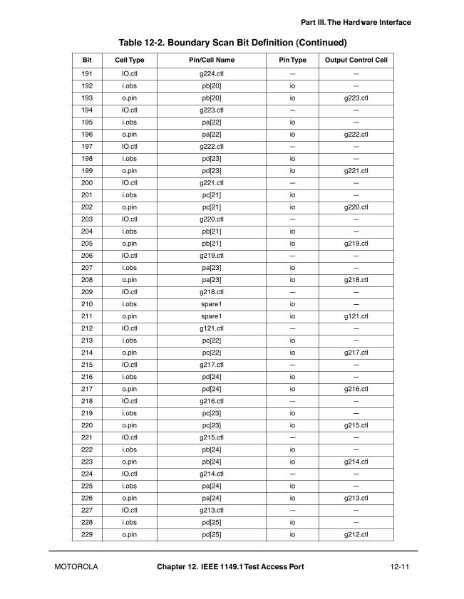
Part III. The Hardware Interface
191 IO.ctl g224.ctl Ñ Ñ
192 i.obs pb[20] io Ñ
193 o.pin pb[20] io g223.ctl
194 IO.ctl g223.ctl Ñ Ñ
195 i.obs pa[22] io Ñ
196 o.pin pa[22] io g222.ctl
197 IO.ctl g222.ctl Ñ Ñ
198 i.obs pd[23] io Ñ
199 o.pin pd[23] io g221.ctl
200 IO.ctl g221.ctl Ñ Ñ
201 i.obs pc[21] io Ñ
202 o.pin pc[21] io g220.ctl
203 IO.ctl g220.ctl Ñ Ñ
204 i.obs pb[21] io Ñ
205 o.pin pb[21] io g219.ctl
206 IO.ctl g219.ctl Ñ Ñ
207 i.obs pa[23] io Ñ
208 o.pin pa[23] io g218.ctl
209 IO.ctl g218.ctl Ñ Ñ
210 i.obs spare1 io Ñ
211 o.pin spare1 io g121.ctl
212 IO.ctl g121.ctl Ñ Ñ
213 i.obs pc[22] io Ñ
214 o.pin pc[22] io g217.ctl
215 IO.ctl g217.ctl Ñ Ñ
216 i.obs pd[24] io Ñ
217 o.pin pd[24] io g216.ctl
218 IO.ctl g216.ctl Ñ Ñ
219 i.obs pc[23] io Ñ
220 o.pin pc[23] io g215.ctl
221 IO.ctl g215.ctl Ñ Ñ
222 i.obs pb[24] io Ñ
223 o.pin pb[24] io g214.ctl
224 IO.ctl g214.ctl Ñ Ñ
225 i.obs pa[24] io Ñ
226 o.pin pa[24] io g213.ctl
227 IO.ctl g213.ctl Ñ Ñ
228 i.obs pd[25] io Ñ
229 o.pin pd[25] io g212.ctl
Table 12-2. Boundary Scan Bit Definition (Continued)
Bit Cell Type Pin/Cell Name Pin Type Output Control Cell
MOTOROLA Chapter 12. IEEE 1149.1 Test Access Port 12-11
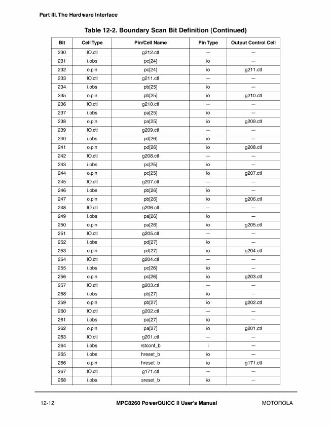
Part III. The Hardware Interface
230 IO.ctl g212.ctl Ñ Ñ
231 i.obs pc[24] io Ñ
232 o.pin pc[24] io g211.ctl
233 IO.ctl g211.ctl Ñ Ñ
234 i.obs pb[25] io Ñ
235 o.pin pb[25] io g210.ctl
236 IO.ctl g210.ctl Ñ Ñ
237 i.obs pa[25] io Ñ
238 o.pin pa[25] io g209.ctl
239 IO.ctl g209.ctl Ñ Ñ
240 i.obs pd[26] io Ñ
241 o.pin pd[26] io g208.ctl
242 IO.ctl g208.ctl Ñ Ñ
243 i.obs pc[25] io Ñ
244 o.pin pc[25] io g207.ctl
245 IO.ctl g207.ctl Ñ Ñ
246 i.obs pb[26] io Ñ
247 o.pin pb[26] io g206.ctl
248 IO.ctl g206.ctl Ñ Ñ
249 i.obs pa[26] io Ñ
250 o.pin pa[26] io g205.ctl
251 IO.ctl g205.ctl Ñ Ñ
252 i.obs pd[27] io Ñ
253 o.pin pd[27] io g204.ctl
254 IO.ctl g204.ctl Ñ Ñ
255 i.obs pc[26] io Ñ
256 o.pin pc[26] io g203.ctl
257 IO.ctl g203.ctl Ñ Ñ
258 i.obs pb[27] io Ñ
259 o.pin pb[27] io g202.ctl
260 IO.ctl g202.ctl Ñ Ñ
261 i.obs pa[27] io Ñ
262 o.pin pa[27] io g201.ctl
263 IO.ctl g201.ctl Ñ Ñ
264 i.obs rstconf_b i Ñ
265 i.obs hreset_b io Ñ
266 o.pin hreset_b io g171.ctl
267 IO.ctl g171.ctl Ñ Ñ
268 i.obs sreset_b io Ñ
Table 12-2. Boundary Scan Bit Definition (Continued)
Bit Cell Type Pin/Cell Name Pin Type Output Control Cell
12-12 MPC8260 PowerQUICC II UserÕs Manual MOTOROLA

Part III. The Hardware Interface
269 o.pin sreset_b io g170.ctl
270 IO.ctl g170.ctl Ñ Ñ
271 i.obs clkin i Ñ
272 i.obs pc[27] io Ñ
273 o.pin pc[27] io g166.ctl
274 IO.ctl g166.ctl Ñ Ñ
275 i.obs pd[28] io Ñ
276 o.pin pd[28] io g165.ctl
277 IO.ctl g165.ctl Ñ Ñ
278 i.obs pc[28] io Ñ
279 o.pin pc[28] io g164.ctl
280 IO.ctl g164.ctl Ñ Ñ
281 i.obs pb[28] io Ñ
282 o.pin pb[28] io g163.ctl
283 IO.ctl g163.ctl Ñ Ñ
284 i.obs pa[28] io Ñ
285 o.pin pa[28] io g162.ctl
286 IO.ctl g162.ctl Ñ Ñ
287 i.obs pd[29] io Ñ
288 o.pin pd[29] io g161.ctl
289 IO.ctl g161.ctl Ñ Ñ
290 i.obs pc[29] io Ñ
291 o.pin pc[29] io g160.ctl
292 IO.ctl g160.ctl Ñ Ñ
293 i.obs pb[29] io Ñ
294 o.pin pb[29] io g159.ctl
295 IO.ctl g159.ctl Ñ Ñ
296 i.obs pa[29] io Ñ
297 o.pin pa[29] io g158.ctl
298 IO.ctl g158.ctl Ñ Ñ
299 i.obs pd[30] io Ñ
300 o.pin pd[30] io g157.ctl
301 IO.ctl g157.ctl Ñ Ñ
302 i.obs pc[30] io Ñ
303 o.pin pc[30] io g156.ctl
304 IO.ctl g156.ctl Ñ Ñ
305 i.obs pb[30] io Ñ
306 o.pin pb[30] io g155.ctl
307 IO.ctl g155.ctl Ñ Ñ
Table 12-2. Boundary Scan Bit Definition (Continued)
Bit Cell Type Pin/Cell Name Pin Type Output Control Cell
MOTOROLA Chapter 12. IEEE 1149.1 Test Access Port 12-13
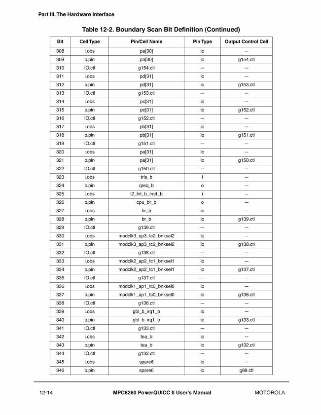
Part III. The Hardware Interface
308 i.obs pa[30] io Ñ
309 o.pin pa[30] io g154.ctl
310 IO.ctl g154.ctl Ñ Ñ
311 i.obs pd[31] io Ñ
312 o.pin pd[31] io g153.ctl
313 IO.ctl g153.ctl Ñ Ñ
314 i.obs pc[31] io Ñ
315 o.pin pc[31] io g152.ctl
316 IO.ctl g152.ctl Ñ Ñ
317 i.obs pb[31] io Ñ
318 o.pin pb[31] io g151.ctl
319 IO.ctl g151.ctl Ñ Ñ
320 i.obs pa[31] io Ñ
321 o.pin pa[31] io g150.ctl
322 IO.ctl g150.ctl Ñ Ñ
323 i.obs tris_b i Ñ
324 o.pin qreq_b o Ñ
325 i.obs l2_hit_b_irq4_b i Ñ
326 o.pin cpu_br_b o Ñ
327 i.obs br_b io Ñ
328 o.pin br_b io g139.ctl
329 IO.ctl g139.ctl Ñ Ñ
330 i.obs modclk3_ap3_tc2_bnksel2 io Ñ
331 o.pin modclk3_ap3_tc2_bnksel2 io g138.ctl
332 IO.ctl g138.ctl Ñ Ñ
333 i.obs modclk2_ap2_tc1_bnksel1 io Ñ
334 o.pin modclk2_ap2_tc1_bnksel1 io g137.ctl
335 IO.ctl g137.ctl Ñ Ñ
336 i.obs modclk1_ap1_tc0_bnksel0 io Ñ
337 o.pin modclk1_ap1_tc0_bnksel0 io g136.ctl
338 IO.ctl g136.ctl Ñ Ñ
339 i.obs gbl_b_irq1_b io Ñ
340 o.pin gbl_b_irq1_b io g133.ctl
341 IO.ctl g133.ctl Ñ Ñ
342 i.obs tea_b io Ñ
343 o.pin tea_b io g132.ctl
344 IO.ctl g132.ctl Ñ Ñ
345 i.obs spare6 io Ñ
346 o.pin spare6 io g89.ctl
Table 12-2. Boundary Scan Bit Definition (Continued)
Bit Cell Type Pin/Cell Name Pin Type Output Control Cell
12-14 MPC8260 PowerQUICC II UserÕs Manual MOTOROLA
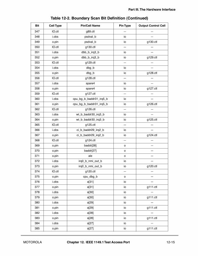
Part III. The Hardware Interface
347 IO.ctl g89.ctl Ñ Ñ
348 i.obs psdval_b io Ñ
349 o.pin psdval_b io g130.ctl
350 IO.ctl g130.ctl Ñ Ñ
351 i.obs dbb_b_irq3_b io Ñ
352 o.pin dbb_b_irq3_b io g129.ctl
353 IO.ctl g129.ctl Ñ Ñ
354 i.obs dbg_b io Ñ
355 o.pin dbg_b io g128.ctl
356 IO.ctl g128.ctl Ñ Ñ
357 i.obs spare4 io Ñ
358 o.pin spare4 io g127.ctl
359 IO.ctl g127.ctl Ñ Ñ
360 i.obs cpu_bg_b_baddr31_irq5_b io Ñ
361 o.pin cpu_bg_b_baddr31_irq5_b io g126.ctl
362 IO.ctl g126.ctl Ñ Ñ
363 i.obs wt_b_baddr30_irq3_b io Ñ
364 o.pin wt_b_baddr30_irq3_b io g125.ctl
365 IO.ctl g125.ctl Ñ Ñ
366 i.obs ci_b_baddr29_irq2_b io Ñ
367 o.pin ci_b_baddr29_irq2_b io g124.ctl
368 IO.ctl g124.ctl Ñ Ñ
369 o.pin baddr[28] o Ñ
370 o.pin baddr[27] o Ñ
371 o.pin ale o Ñ
372 i.obs irq0_b_nmi_out_b io Ñ
373 o.pin irq0_b_nmi_out_b io g120.ctl
374 IO.ctl g120.ctl Ñ Ñ
375 o.pin cpu_dbg_b o Ñ
376 i.obs a[31] io Ñ
377 o.pin a[31] io g111.ctl
378 i.obs a[30] io Ñ
379 o.pin a[30] io g111.ctl
380 i.obs a[29] io Ñ
381 o.pin a[29] io g111.ctl
382 i.obs a[28] io Ñ
383 o.pin a[28] io g111.ctl
384 i.obs a[27] io Ñ
385 o.pin a[27] io g111.ctl
Table 12-2. Boundary Scan Bit Definition (Continued)
Bit Cell Type Pin/Cell Name Pin Type Output Control Cell
MOTOROLA Chapter 12. IEEE 1149.1 Test Access Port 12-15
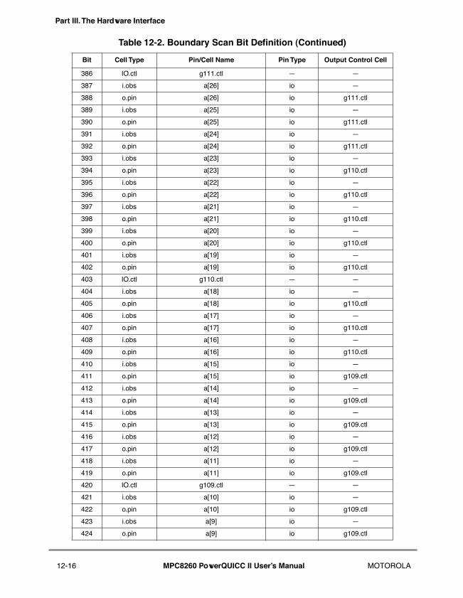
Part III. The Hardware Interface
386 IO.ctl g111.ctl Ñ Ñ
387 i.obs a[26] io Ñ
388 o.pin a[26] io g111.ctl
389 i.obs a[25] io Ñ
390 o.pin a[25] io g111.ctl
391 i.obs a[24] io Ñ
392 o.pin a[24] io g111.ctl
393 i.obs a[23] io Ñ
394 o.pin a[23] io g110.ctl
395 i.obs a[22] io Ñ
396 o.pin a[22] io g110.ctl
397 i.obs a[21] io Ñ
398 o.pin a[21] io g110.ctl
399 i.obs a[20] io Ñ
400 o.pin a[20] io g110.ctl
401 i.obs a[19] io Ñ
402 o.pin a[19] io g110.ctl
403 IO.ctl g110.ctl Ñ Ñ
404 i.obs a[18] io Ñ
405 o.pin a[18] io g110.ctl
406 i.obs a[17] io Ñ
407 o.pin a[17] io g110.ctl
408 i.obs a[16] io Ñ
409 o.pin a[16] io g110.ctl
410 i.obs a[15] io Ñ
411 o.pin a[15] io g109.ctl
412 i.obs a[14] io Ñ
413 o.pin a[14] io g109.ctl
414 i.obs a[13] io Ñ
415 o.pin a[13] io g109.ctl
416 i.obs a[12] io Ñ
417 o.pin a[12] io g109.ctl
418 i.obs a[11] io Ñ
419 o.pin a[11] io g109.ctl
420 IO.ctl g109.ctl Ñ Ñ
421 i.obs a[10] io Ñ
422 o.pin a[10] io g109.ctl
423 i.obs a[9] io Ñ
424 o.pin a[9] io g109.ctl
Table 12-2. Boundary Scan Bit Definition (Continued)
Bit Cell Type Pin/Cell Name Pin Type Output Control Cell
12-16 MPC8260 PowerQUICC II UserÕs Manual MOTOROLA
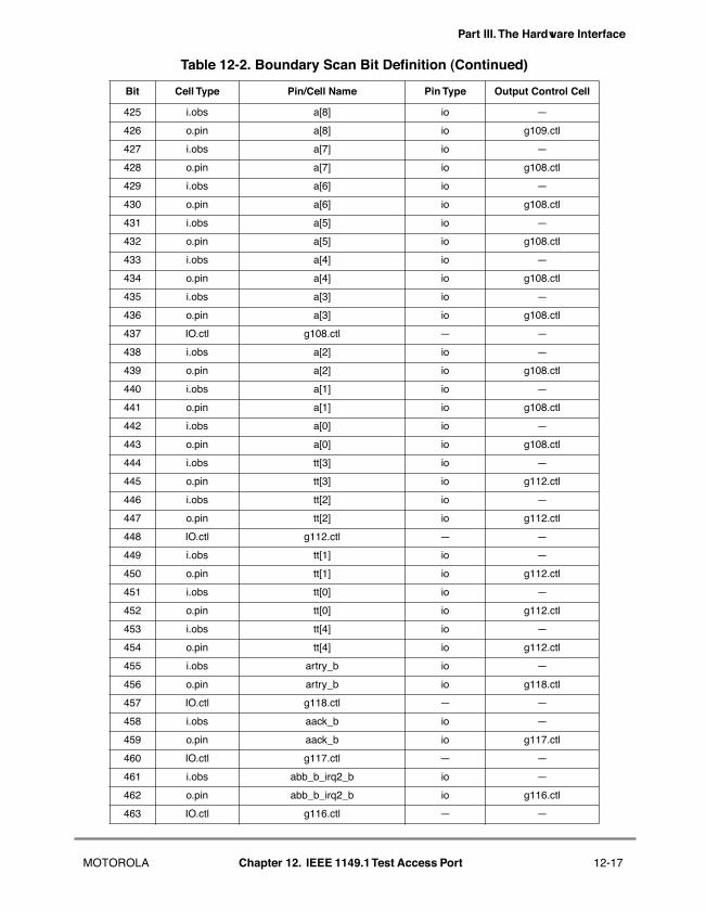
Part III. The Hardware Interface
425 i.obs a[8] io Ñ
426 o.pin a[8] io g109.ctl
427 i.obs a[7] io Ñ
428 o.pin a[7] io g108.ctl
429 i.obs a[6] io Ñ
430 o.pin a[6] io g108.ctl
431 i.obs a[5] io Ñ
432 o.pin a[5] io g108.ctl
433 i.obs a[4] io Ñ
434 o.pin a[4] io g108.ctl
435 i.obs a[3] io Ñ
436 o.pin a[3] io g108.ctl
437 IO.ctl g108.ctl Ñ Ñ
438 i.obs a[2] io Ñ
439 o.pin a[2] io g108.ctl
440 i.obs a[1] io Ñ
441 o.pin a[1] io g108.ctl
442 i.obs a[0] io Ñ
443 o.pin a[0] io g108.ctl
444 i.obs tt[3] io Ñ
445 o.pin tt[3] io g112.ctl
446 i.obs tt[2] io Ñ
447 o.pin tt[2] io g112.ctl
448 IO.ctl g112.ctl Ñ Ñ
449 i.obs tt[1] io Ñ
450 o.pin tt[1] io g112.ctl
451 i.obs tt[0] io Ñ
452 o.pin tt[0] io g112.ctl
453 i.obs tt[4] io Ñ
454 o.pin tt[4] io g112.ctl
455 i.obs artry_b io Ñ
456 o.pin artry_b io g118.ctl
457 IO.ctl g118.ctl Ñ Ñ
458 i.obs aack_b io Ñ
459 o.pin aack_b io g117.ctl
460 IO.ctl g117.ctl Ñ Ñ
461 i.obs abb_b_irq2_b io Ñ
462 o.pin abb_b_irq2_b io g116.ctl
463 IO.ctl g116.ctl Ñ Ñ
Table 12-2. Boundary Scan Bit Definition (Continued)
Bit Cell Type Pin/Cell Name Pin Type Output Control Cell
MOTOROLA Chapter 12. IEEE 1149.1 Test Access Port 12-17
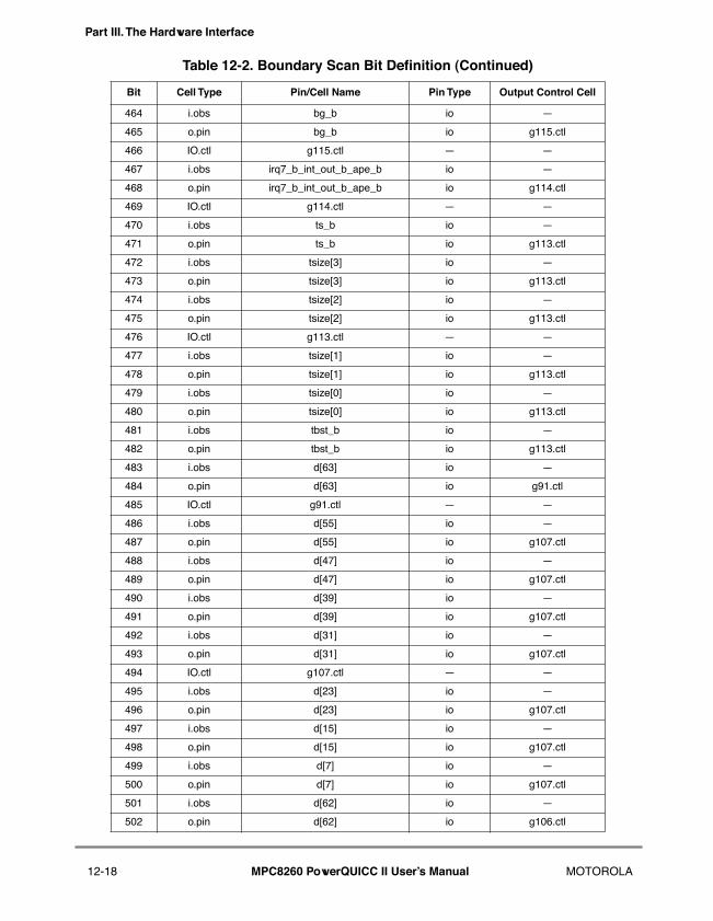
Part III. The Hardware Interface
464 i.obs bg_b io Ñ
465 o.pin bg_b io g115.ctl
466 IO.ctl g115.ctl Ñ Ñ
467 i.obs irq7_b_int_out_b_ape_b io Ñ
468 o.pin irq7_b_int_out_b_ape_b io g114.ctl
469 IO.ctl g114.ctl Ñ Ñ
470 i.obs ts_b io Ñ
471 o.pin ts_b io g113.ctl
472 i.obs tsize[3] io Ñ
473 o.pin tsize[3] io g113.ctl
474 i.obs tsize[2] io Ñ
475 o.pin tsize[2] io g113.ctl
476 IO.ctl g113.ctl Ñ Ñ
477 i.obs tsize[1] io Ñ
478 o.pin tsize[1] io g113.ctl
479 i.obs tsize[0] io Ñ
480 o.pin tsize[0] io g113.ctl
481 i.obs tbst_b io Ñ
482 o.pin tbst_b io g113.ctl
483 i.obs d[63] io Ñ
484 o.pin d[63] io g91.ctl
485 IO.ctl g91.ctl Ñ Ñ
486 i.obs d[55] io Ñ
487 o.pin d[55] io g107.ctl
488 i.obs d[47] io Ñ
489 o.pin d[47] io g107.ctl
490 i.obs d[39] io Ñ
491 o.pin d[39] io g107.ctl
492 i.obs d[31] io Ñ
493 o.pin d[31] io g107.ctl
494 IO.ctl g107.ctl Ñ Ñ
495 i.obs d[23] io Ñ
496 o.pin d[23] io g107.ctl
497 i.obs d[15] io Ñ
498 o.pin d[15] io g107.ctl
499 i.obs d[7] io Ñ
500 o.pin d[7] io g107.ctl
501 i.obs d[62] io Ñ
502 o.pin d[62] io g106.ctl
Table 12-2. Boundary Scan Bit Definition (Continued)
Bit Cell Type Pin/Cell Name Pin Type Output Control Cell
12-18 MPC8260 PowerQUICC II UserÕs Manual MOTOROLA
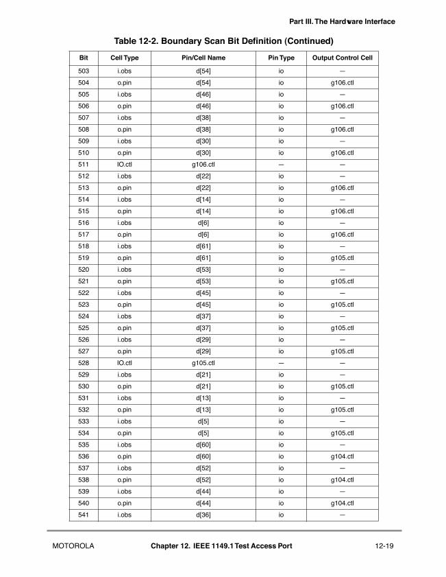
Part III. The Hardware Interface
503 i.obs d[54] io Ñ
504 o.pin d[54] io g106.ctl
505 i.obs d[46] io Ñ
506 o.pin d[46] io g106.ctl
507 i.obs d[38] io Ñ
508 o.pin d[38] io g106.ctl
509 i.obs d[30] io Ñ
510 o.pin d[30] io g106.ctl
511 IO.ctl g106.ctl Ñ Ñ
512 i.obs d[22] io Ñ
513 o.pin d[22] io g106.ctl
514 i.obs d[14] io Ñ
515 o.pin d[14] io g106.ctl
516 i.obs d[6] io Ñ
517 o.pin d[6] io g106.ctl
518 i.obs d[61] io Ñ
519 o.pin d[61] io g105.ctl
520 i.obs d[53] io Ñ
521 o.pin d[53] io g105.ctl
522 i.obs d[45] io Ñ
523 o.pin d[45] io g105.ctl
524 i.obs d[37] io Ñ
525 o.pin d[37] io g105.ctl
526 i.obs d[29] io Ñ
527 o.pin d[29] io g105.ctl
528 IO.ctl g105.ctl Ñ Ñ
529 i.obs d[21] io Ñ
530 o.pin d[21] io g105.ctl
531 i.obs d[13] io Ñ
532 o.pin d[13] io g105.ctl
533 i.obs d[5] io Ñ
534 o.pin d[5] io g105.ctl
535 i.obs d[60] io Ñ
536 o.pin d[60] io g104.ctl
537 i.obs d[52] io Ñ
538 o.pin d[52] io g104.ctl
539 i.obs d[44] io Ñ
540 o.pin d[44] io g104.ctl
541 i.obs d[36] io Ñ
Table 12-2. Boundary Scan Bit Definition (Continued)
Bit Cell Type Pin/Cell Name Pin Type Output Control Cell
MOTOROLA Chapter 12. IEEE 1149.1 Test Access Port 12-19
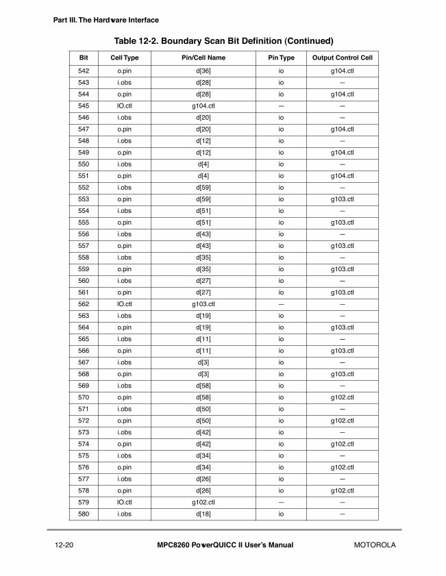
Part III. The Hardware Interface
542 o.pin d[36] io g104.ctl
543 i.obs d[28] io Ñ
544 o.pin d[28] io g104.ctl
545 IO.ctl g104.ctl Ñ Ñ
546 i.obs d[20] io Ñ
547 o.pin d[20] io g104.ctl
548 i.obs d[12] io Ñ
549 o.pin d[12] io g104.ctl
550 i.obs d[4] io Ñ
551 o.pin d[4] io g104.ctl
552 i.obs d[59] io Ñ
553 o.pin d[59] io g103.ctl
554 i.obs d[51] io Ñ
555 o.pin d[51] io g103.ctl
556 i.obs d[43] io Ñ
557 o.pin d[43] io g103.ctl
558 i.obs d[35] io Ñ
559 o.pin d[35] io g103.ctl
560 i.obs d[27] io Ñ
561 o.pin d[27] io g103.ctl
562 IO.ctl g103.ctl Ñ Ñ
563 i.obs d[19] io Ñ
564 o.pin d[19] io g103.ctl
565 i.obs d[11] io Ñ
566 o.pin d[11] io g103.ctl
567 i.obs d[3] io Ñ
568 o.pin d[3] io g103.ctl
569 i.obs d[58] io Ñ
570 o.pin d[58] io g102.ctl
571 i.obs d[50] io Ñ
572 o.pin d[50] io g102.ctl
573 i.obs d[42] io Ñ
574 o.pin d[42] io g102.ctl
575 i.obs d[34] io Ñ
576 o.pin d[34] io g102.ctl
577 i.obs d[26] io Ñ
578 o.pin d[26] io g102.ctl
579 IO.ctl g102.ctl Ñ Ñ
580 i.obs d[18] io Ñ
Table 12-2. Boundary Scan Bit Definition (Continued)
Bit Cell Type Pin/Cell Name Pin Type Output Control Cell
12-20 MPC8260 PowerQUICC II UserÕs Manual MOTOROLA
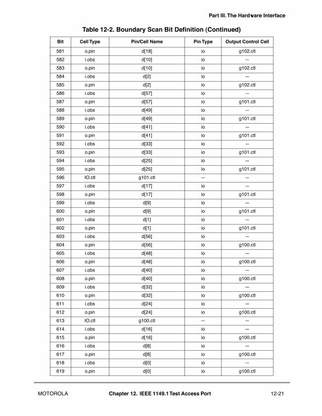
Part III. The Hardware Interface
581 o.pin d[18] io g102.ctl
582 i.obs d[10] io Ñ
583 o.pin d[10] io g102.ctl
584 i.obs d[2] io Ñ
585 o.pin d[2] io g102.ctl
586 i.obs d[57] io Ñ
587 o.pin d[57] io g101.ctl
588 i.obs d[49] io Ñ
589 o.pin d[49] io g101.ctl
590 i.obs d[41] io Ñ
591 o.pin d[41] io g101.ctl
592 i.obs d[33] io Ñ
593 o.pin d[33] io g101.ctl
594 i.obs d[25] io Ñ
595 o.pin d[25] io g101.ctl
596 IO.ctl g101.ctl Ñ Ñ
597 i.obs d[17] io Ñ
598 o.pin d[17] io g101.ctl
599 i.obs d[9] io Ñ
600 o.pin d[9] io g101.ctl
601 i.obs d[1] io Ñ
602 o.pin d[1] io g101.ctl
603 i.obs d[56] io Ñ
604 o.pin d[56] io g100.ctl
605 i.obs d[48] io Ñ
606 o.pin d[48] io g100.ctl
607 i.obs d[40] io Ñ
608 o.pin d[40] io g100.ctl
609 i.obs d[32] io Ñ
610 o.pin d[32] io g100.ctl
611 i.obs d[24] io Ñ
612 o.pin d[24] io g100.ctl
613 IO.ctl g100.ctl Ñ Ñ
614 i.obs d[16] io Ñ
615 o.pin d[16] io g100.ctl
616 i.obs d[8] io Ñ
617 o.pin d[8] io g100.ctl
618 i.obs d[0] io Ñ
619 o.pin d[0] io g100.ctl
Table 12-2. Boundary Scan Bit Definition (Continued)
Bit Cell Type Pin/Cell Name Pin Type Output Control Cell
MOTOROLA Chapter 12. IEEE 1149.1 Test Access Port 12-21
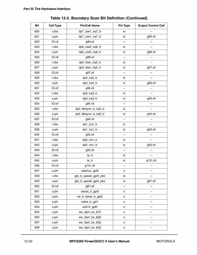
Part III. The Hardware Interface
620 i.obs dp7_cse1_irq7_b io Ñ
621 o.pin dp7_cse1_irq7_b io g99.ctl
622 IO.ctl g99.ctl Ñ Ñ
623 i.obs dp6_cse0_irq6_b io Ñ
624 o.pin dp6_cse0_irq6_b io g98.ctl
625 IO.ctl g98.ctl Ñ Ñ
626 i.obs dp5_tben_irq5_b io Ñ
627 o.pin dp5_tben_irq5_b io g97.ctl
628 IO.ctl g97.ctl Ñ Ñ
629 i.obs dp4_irq4_b io Ñ
630 o.pin dp4_irq4_b io g96.ctl
631 IO.ctl g96.ctl Ñ Ñ
632 i.obs dp3_irq3_b io Ñ
633 o.pin dp3_irq3_b io g95.ctl
634 IO.ctl g95.ctl Ñ Ñ
635 i.obs dp2_tlbisync_b_irq2_b io Ñ
636 o.pin dp2_tlbisync_b_irq2_b io g94.ctl
637 IO.ctl g94.ctl Ñ Ñ
638 i.obs dp1_irq1_b io Ñ
639 o.pin dp1_irq1_b io g93.ctl
640 IO.ctl g93.ctl Ñ Ñ
641 i.obs dp0_rsrv_b io Ñ
642 o.pin dp0_rsrv_b io g92.ctl
643 IO.ctl g92.ctl Ñ Ñ
644 i.obs ta_b io Ñ
645 o.pin ta_b io g131.ctl
646 IO.ctl g131.ctl Ñ Ñ
647 o.pin sdamux_gpl5 o Ñ
648 i.obs gta_b_upwait_gpl4_pbs io Ñ
649 o.pin gta_b_upwait_gpl4_pbs io g87.ctl
650 IO.ctl g87.ctl Ñ Ñ
651 o.pin sdcas_b_gpl3 o Ñ
652 o.pin oe_b_sdras_b_gpl2 o Ñ
653 o.pin sdwe_b_gpl1 o Ñ
654 o.pin sda10_gpl0 o Ñ
655 o.pin we_dqm_bs_b[7] o Ñ
656 o.pin we_dqm_bs_b[6] o Ñ
657 o.pin we_dqm_bs_b[5] o Ñ
658 o.pin we_dqm_bs_b[4] o Ñ
Table 12-2. Boundary Scan Bit Definition (Continued)
Bit Cell Type Pin/Cell Name Pin Type Output Control Cell
12-22 MPC8260 PowerQUICC II UserÕs Manual MOTOROLA
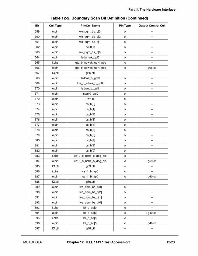
Part III. The Hardware Interface
659 o.pin we_dqm_bs_b[3] o Ñ
660 o.pin we_dqm_bs_b[2] o Ñ
661 o.pin we_dqm_bs_b[1] o Ñ
662 o.pin bctl0_b o Ñ
663 o.pin we_dqm_bs_b[0] o Ñ
664 o.pin lsdamux_gpl5 o Ñ
665 i.obs lgta_b_upwait_gpl4_pbs io Ñ
666 o.pin lgta_b_upwait_gpl4_pbs io g66.ctl
667 IO.ctl g66.ctl Ñ Ñ
668 o.pin lsdcas_b_gpl3 o Ñ
669 o.pin loe_b_sdras_b_gpl2 o Ñ
670 o.pin lsdwe_b_gpl1 o Ñ
671 o.pin lsda10_gpl0 o Ñ
672 o.pin lwr_b o Ñ
673 o.pin cs_b[0] o Ñ
674 o.pin cs_b[1] o Ñ
675 o.pin cs_b[2] o Ñ
676 o.pin cs_b[3] o Ñ
677 o.pin cs_b[4] o Ñ
678 o.pin cs_b[5] o Ñ
679 o.pin cs_b[6] o Ñ
680 o.pin cs_b[7] o Ñ
681 o.pin cs_b[8] o Ñ
682 o.pin cs_b[9] o Ñ
683 i.obs cs10_b_bctl1_b_dbg_dis io Ñ
684 o.pin cs10_b_bctl1_b_dbg_dis io g59.ctl
685 IO.ctl g59.ctl Ñ Ñ
686 i.obs cs11_b_ap0 io Ñ
687 o.pin cs11_b_ap0 io g60.ctl
688 IO.ctl g60.ctl Ñ Ñ
689 o.pin lwe_dqm_bs_b[3] o Ñ
690 o.pin lwe_dqm_bs_b[2] o Ñ
691 o.pin lwe_dqm_bs_b[1] o Ñ
692 o.pin lwe_dqm_bs_b[0] o Ñ
693 i.obs lcl_d_ad[0] io Ñ
694 o.pin lcl_d_ad[0] io g40.ctl
695 i.obs lcl_d_ad[5] io Ñ
696 o.pin lcl_d_ad[5] io g48.ctl
697 IO.ctl g48.ctl Ñ Ñ
Table 12-2. Boundary Scan Bit Definition (Continued)
Bit Cell Type Pin/Cell Name Pin Type Output Control Cell
MOTOROLA Chapter 12. IEEE 1149.1 Test Access Port 12-23
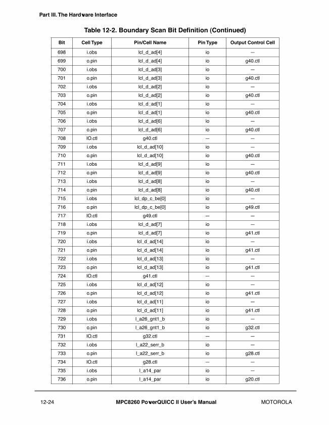
Part III. The Hardware Interface
698 i.obs lcl_d_ad[4] io Ñ
699 o.pin lcl_d_ad[4] io g40.ctl
700 i.obs lcl_d_ad[3] io Ñ
701 o.pin lcl_d_ad[3] io g40.ctl
702 i.obs lcl_d_ad[2] io Ñ
703 o.pin lcl_d_ad[2] io g40.ctl
704 i.obs lcl_d_ad[1] io Ñ
705 o.pin lcl_d_ad[1] io g40.ctl
706 i.obs lcl_d_ad[6] io Ñ
707 o.pin lcl_d_ad[6] io g40.ctl
708 IO.ctl g40.ctl Ñ Ñ
709 i.obs lcl_d_ad[10] io Ñ
710 o.pin lcl_d_ad[10] io g40.ctl
711 i.obs lcl_d_ad[9] io Ñ
712 o.pin lcl_d_ad[9] io g40.ctl
713 i.obs lcl_d_ad[8] io Ñ
714 o.pin lcl_d_ad[8] io g40.ctl
715 i.obs lcl_dp_c_be[0] io Ñ
716 o.pin lcl_dp_c_be[0] io g49.ctl
717 IO.ctl g49.ctl Ñ Ñ
718 i.obs lcl_d_ad[7] io Ñ
719 o.pin lcl_d_ad[7] io g41.ctl
720 i.obs lcl_d_ad[14] io Ñ
721 o.pin lcl_d_ad[14] io g41.ctl
722 i.obs lcl_d_ad[13] io Ñ
723 o.pin lcl_d_ad[13] io g41.ctl
724 IO.ctl g41.ctl Ñ Ñ
725 i.obs lcl_d_ad[12] io Ñ
726 o.pin lcl_d_ad[12] io g41.ctl
727 i.obs lcl_d_ad[11] io Ñ
728 o.pin lcl_d_ad[11] io g41.ctl
729 i.obs l_a26_gnt1_b io Ñ
730 o.pin l_a26_gnt1_b io g32.ctl
731 IO.ctl g32.ctl Ñ Ñ
732 i.obs l_a22_serr_b io Ñ
733 o.pin l_a22_serr_b io g28.ctl
734 IO.ctl g28.ctl Ñ Ñ
735 i.obs l_a14_par io Ñ
736 o.pin l_a14_par io g20.ctl
Table 12-2. Boundary Scan Bit Definition (Continued)
Bit Cell Type Pin/Cell Name Pin Type Output Control Cell
12-24 MPC8260 PowerQUICC II UserÕs Manual MOTOROLA

Part III. The Hardware Interface
737 IO.ctl g20.ctl Ñ Ñ
738 i.obs lcl_dp_c_be[1] io Ñ
739 o.pin lcl_dp_c_be[1] io g44.ctl
740 IO.ctl g44.ctl Ñ Ñ
741 i.obs lcl_d_ad[15] io Ñ
742 o.pin lcl_d_ad[15] io g47.ctl
743 IO.ctl g47.ctl Ñ Ñ
744 i.obs l_a30_lock_b io Ñ
745 o.pin l_a30_lock_b io g36.ctl
746 IO.ctl g36.ctl Ñ Ñ
747 i.obs l_a21_perr_b io Ñ
748 o.pin l_a21_perr_b io g27.ctl
749 IO.ctl g27.ctl Ñ Ñ
750 i.obs l_a24_req1_b io Ñ
751 o.pin l_a24_req1_b io g30.ctl
752 IO.ctl g30.ctl Ñ Ñ
753 i.obs l_a19_devsel_b io Ñ
754 o.pin l_a19_devsel_b io g25.ctl
755 IO.ctl g25.ctl Ñ Ñ
756 i.obs l_a17_irdy_b_ckstp_out io Ñ
757 o.pin l_a17_irdy_b_ckstp_out io g23.ctl
758 IO.ctl g23.ctl Ñ Ñ
759 i.obs l_a16_trdy_b io Ñ
760 o.pin l_a16_trdy_b io g22.ctl
761 IO.ctl g22.ctl Ñ Ñ
762 i.obs l_a18_stop_b io Ñ
763 o.pin l_a18_stop_b io g24.ctl
764 IO.ctl g24.ctl Ñ Ñ
765 i.obs l_a15_frm_b_smi_b io Ñ
766 o.pin l_a15_frm_b_smi_b io g21.ctl
767 IO.ctl g21.ctl Ñ Ñ
768 i.obs lcl_dp_c_be[2] io Ñ
769 o.pin lcl_dp_c_be[2] io g46.ctl
770 IO.ctl g46.ctl Ñ Ñ
771 i.obs lcl_d_ad[16] io Ñ
772 o.pin lcl_d_ad[16] io g42.ctl
773 i.obs lcl_d_ad[17] io Ñ
774 o.pin lcl_d_ad[17] io g42.ctl
775 i.obs lcl_d_ad[18] io Ñ
Table 12-2. Boundary Scan Bit Definition (Continued)
Bit Cell Type Pin/Cell Name Pin Type Output Control Cell
MOTOROLA Chapter 12. IEEE 1149.1 Test Access Port 12-25
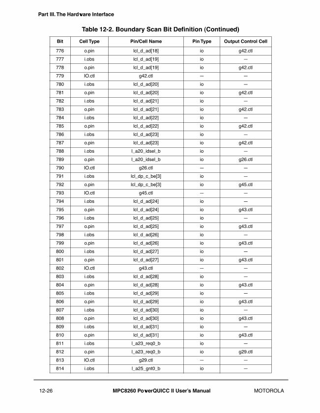
Part III. The Hardware Interface
776 o.pin lcl_d_ad[18] io g42.ctl
777 i.obs lcl_d_ad[19] io Ñ
778 o.pin lcl_d_ad[19] io g42.ctl
779 IO.ctl g42.ctl Ñ Ñ
780 i.obs lcl_d_ad[20] io Ñ
781 o.pin lcl_d_ad[20] io g42.ctl
782 i.obs lcl_d_ad[21] io Ñ
783 o.pin lcl_d_ad[21] io g42.ctl
784 i.obs lcl_d_ad[22] io Ñ
785 o.pin lcl_d_ad[22] io g42.ctl
786 i.obs lcl_d_ad[23] io Ñ
787 o.pin lcl_d_ad[23] io g42.ctl
788 i.obs l_a20_idsel_b io Ñ
789 o.pin l_a20_idsel_b io g26.ctl
790 IO.ctl g26.ctl Ñ Ñ
791 i.obs lcl_dp_c_be[3] io Ñ
792 o.pin lcl_dp_c_be[3] io g45.ctl
793 IO.ctl g45.ctl Ñ Ñ
794 i.obs lcl_d_ad[24] io Ñ
795 o.pin lcl_d_ad[24] io g43.ctl
796 i.obs lcl_d_ad[25] io Ñ
797 o.pin lcl_d_ad[25] io g43.ctl
798 i.obs lcl_d_ad[26] io Ñ
799 o.pin lcl_d_ad[26] io g43.ctl
800 i.obs lcl_d_ad[27] io Ñ
801 o.pin lcl_d_ad[27] io g43.ctl
802 IO.ctl g43.ctl Ñ Ñ
803 i.obs lcl_d_ad[28] io Ñ
804 o.pin lcl_d_ad[28] io g43.ctl
805 i.obs lcl_d_ad[29] io Ñ
806 o.pin lcl_d_ad[29] io g43.ctl
807 i.obs lcl_d_ad[30] io Ñ
808 o.pin lcl_d_ad[30] io g43.ctl
809 i.obs lcl_d_ad[31] io Ñ
810 o.pin lcl_d_ad[31] io g43.ctl
811 i.obs l_a23_req0_b io Ñ
812 o.pin l_a23_req0_b io g29.ctl
813 IO.ctl g29.ctl Ñ Ñ
814 i.obs l_a25_gnt0_b io Ñ
Table 12-2. Boundary Scan Bit Definition (Continued)
Bit Cell Type Pin/Cell Name Pin Type Output Control Cell
12-26 MPC8260 PowerQUICC II UserÕs Manual MOTOROLA
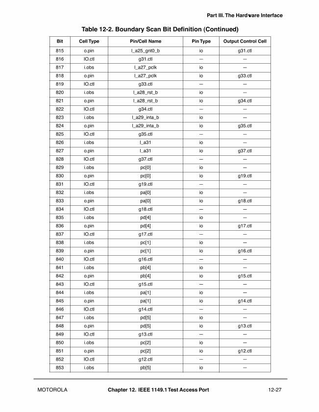
Part III. The Hardware Interface
815 o.pin l_a25_gnt0_b io g31.ctl
816 IO.ctl g31.ctl Ñ Ñ
817 i.obs l_a27_pclk io Ñ
818 o.pin l_a27_pclk io g33.ctl
819 IO.ctl g33.ctl Ñ Ñ
820 i.obs l_a28_rst_b io Ñ
821 o.pin l_a28_rst_b io g34.ctl
822 IO.ctl g34.ctl Ñ Ñ
823 i.obs l_a29_inta_b io Ñ
824 o.pin l_a29_inta_b io g35.ctl
825 IO.ctl g35.ctl Ñ Ñ
826 i.obs l_a31 io Ñ
827 o.pin l_a31 io g37.ctl
828 IO.ctl g37.ctl Ñ Ñ
829 i.obs pc[0] io Ñ
830 o.pin pc[0] io g19.ctl
831 IO.ctl g19.ctl Ñ Ñ
832 i.obs pa[0] io Ñ
833 o.pin pa[0] io g18.ctl
834 IO.ctl g18.ctl Ñ Ñ
835 i.obs pd[4] io Ñ
836 o.pin pd[4] io g17.ctl
837 IO.ctl g17.ctl Ñ Ñ
838 i.obs pc[1] io Ñ
839 o.pin pc[1] io g16.ctl
840 IO.ctl g16.ctl Ñ Ñ
841 i.obs pb[4] io Ñ
842 o.pin pb[4] io g15.ctl
843 IO.ctl g15.ctl Ñ Ñ
844 i.obs pa[1] io Ñ
845 o.pin pa[1] io g14.ctl
846 IO.ctl g14.ctl Ñ Ñ
847 i.obs pd[5] io Ñ
848 o.pin pd[5] io g13.ctl
849 IO.ctl g13.ctl Ñ Ñ
850 i.obs pc[2] io Ñ
851 o.pin pc[2] io g12.ctl
852 IO.ctl g12.ctl Ñ Ñ
853 i.obs pb[5] io Ñ
Table 12-2. Boundary Scan Bit Definition (Continued)
Bit Cell Type Pin/Cell Name Pin Type Output Control Cell
MOTOROLA Chapter 12. IEEE 1149.1 Test Access Port 12-27
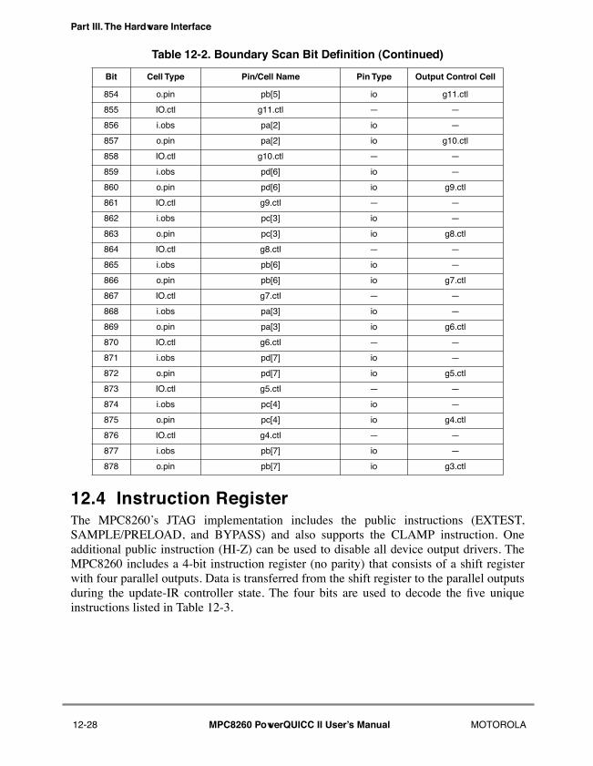
Part III. The Hardware Interface
12.4 Instruction RegisterThe MPC8260Õs JTAG implementation includes the public instructions (EXTEST,SAMPLE/PRELOAD, and BYPASS) and also supports the CLAMP instruction. Oneadditional public instruction (HI-Z) can be used to disable all device output drivers. TheMPC8260 includes a 4-bit instruction register (no parity) that consists of a shift registerwith four parallel outputs. Data is transferred from the shift register to the parallel outputsduring the update-IR controller state. The four bits are used to decode the Þve uniqueinstructions listed in Table 12-3.
854 o.pin pb[5] io g11.ctl
855 IO.ctl g11.ctl Ñ Ñ
856 i.obs pa[2] io Ñ
857 o.pin pa[2] io g10.ctl
858 IO.ctl g10.ctl Ñ Ñ
859 i.obs pd[6] io Ñ
860 o.pin pd[6] io g9.ctl
861 IO.ctl g9.ctl Ñ Ñ
862 i.obs pc[3] io Ñ
863 o.pin pc[3] io g8.ctl
864 IO.ctl g8.ctl Ñ Ñ
865 i.obs pb[6] io Ñ
866 o.pin pb[6] io g7.ctl
867 IO.ctl g7.ctl Ñ Ñ
868 i.obs pa[3] io Ñ
869 o.pin pa[3] io g6.ctl
870 IO.ctl g6.ctl Ñ Ñ
871 i.obs pd[7] io Ñ
872 o.pin pd[7] io g5.ctl
873 IO.ctl g5.ctl Ñ Ñ
874 i.obs pc[4] io Ñ
875 o.pin pc[4] io g4.ctl
876 IO.ctl g4.ctl Ñ Ñ
877 i.obs pb[7] io Ñ
878 o.pin pb[7] io g3.ctl
Table 12-2. Boundary Scan Bit Definition (Continued)
Bit Cell Type Pin/Cell Name Pin Type Output Control Cell
12-28 MPC8260 PowerQUICC II UserÕs Manual MOTOROLA
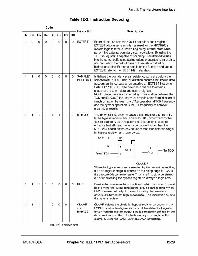
Part III. The Hardware Interface
Table 12-3. Instruction Decoding
CodeInstruction Description
B7 B6 B5 B4 B3 B2 B1 B0
0 0 0 0 0 0 0 0 EXTEST External test. Selects the 475-bit boundary scan register. EXTEST also asserts an internal reset for the MPC8260Õs system logic to force a known beginning internal state while performing external boundary scan operations. By using the TAP, the register is capable of scanning user-deÞned values into the output buffers, capturing values presented to input pins, and controlling the output drive of three-state output or bidirectional pins. For more details on the function and use of EXTEST, refer to the IEEE 1149.1 standard.
1 1 0 0 0 0 0 0 SAMPLE/PRELOAD
Initializes the boundary scan register output cells before the selection of EXTEST. This initialization ensures that known data appears on the outputs when entering an EXTEST instruction. SAMPLE/PRELOAD also provides a chance to obtain a snapshot of system data and control signals.NOTE: Since there is no internal synchronization between the TCK and CLKOUT, the user must provide some form of external synchronization between the JTAG operation at TCK frequency and the system operation CLKOUT frequency to achieve meaningful results.
1 1 1 1 1 1 1 1 BYPASS The BYPASS instruction creates a shift register path from TDI to the bypass register and, Þnally, to TDO, circumventing the 475-bit boundary scan register. This instruction is used to enhance test efÞciency when a component other than the MPC8260 becomes the device under test. It selects the single-bit bypass register as shown below.
When the bypass register is selected by the current instruction, the shift register stage is cleared on the rising edge of TCK in the capture-DR controller state. Thus, the Þrst bit to be shifted out after selecting the bypass register is always a logic zero.
1 1 1 1 0 0 0 0 HIÐZ Provided as a manufacturerÕs optional public instruction to avoid back driving the output pins during circuit-board testing. When HI-Z is invoked all output drivers, including the two-state drivers, are turned off (high impedance). The instruction selects the bypass register.
1 1 1 1 0 0 0 1 CLAMP and BYPASS
CLAMP selects the single-bit bypass register as shown in the BYPASS instruction Þgure above, and the state of all signals driven from the system output pins is completely deÞned by the data previously shifted into the boundary scan register. For example, using the SAMPLE/PRELOAD instruction.
B0 (lsb) is shifted Þrst.
1
1MUX
G1
C
DTo TDO
From TDI
0
Shift DR
Clock DR
MOTOROLA Chapter 12. IEEE 1149.1 Test Access Port 12-29
Part III. The Hardware Interface
The parallel output of the instruction register is set to all ones in the test-logic-resetcontroller state. Notice that this preset state is equivalent to the BYPASS instruction.During the capture-IR controller state, the parallel inputs to the instruction shift register areloaded with the CLAMP command code.12.5 MPC8260 RestrictionsThe control afforded by the output enable signals using the boundary-scan register and theEXTEST instruction requires a compatible circuit-board test environment to avoiddevice-destructive conÞgurations. The user must avoid situations in which the MPC8260Õsoutput drivers are enabled into actively driven networks.
12.6 Nonscan Chain OperationIn nonscan chain operation, the TCK input does not include an internal pull-up resistor andshould be tied high or low to preclude mid-level inputs.
To ensure that the scan chain test logic is kept transparent to the system logic, the TAPcontroller is forced into the test-logic-reset state. This is done inside the chip by connectingTRST to PORESET
TMS should remain connected to Vcc or should not change state, so that the TAP controllerwill not leave the test-logic-reset state.
12-30 MPC8260 PowerQUICC II UserÕs Manual MOTOROLA
Part IVCommunications Processor Module
Intended AudiencePart IV is intended for system designers who need to implement various communicationsprotocols on the MPC8260. It assumes a basic understanding of the PowerPC exceptionmodel, the MPC8260 interrupt structure, as well as a working knowledge of thecommunications protocols to be used. A complete discussion of these protocols is beyondthe scope of this book.
ContentsPart IV describes behavior of the MPC8260 communications processor module (CPM) andthe RISC communications processor (CP) that it contains (note that this is separate fromthe embedded PowerPC processor).
It contains the following chapters:
¥ Chapter 13, ÒCommunications Processor Module Overview,Ó provides a brief overview of the MPC8260 CPM.
¥ Chapter 14, ÒSerial Interface with Time-Slot Assigner,Ó describes the SIU, which controls system start-up, initialization and operation, protection, as well as the external system bus.
¥ Chapter 15, ÒCPM Multiplexing,Ó describes the CPM multiplexing logic (CMX) which connects the physical layerÑUTOPIA, MII, modem lines,
¥ Chapter 16, ÒBaud-Rate Generators (BRGs),Ó describes the eight independent, identical baud-rate generators (BRGs) that can be used with the FCCs, SCCs, and SMCs.
¥ Chapter 17, ÒTimers,Ó describes the MPC8260 timer implementation, which can be conÞgured as four identical 16-bit or two 32-bit general-purpose timers.
¥ Chapter 18, ÒSDMA Channels and IDMA Emulation,Ó describes the two physical serial DMA (SDMA) channels on the MPC8260.
MOTOROLA Part IV. Communications Processor Module Part IV-i
Part IV. Communications Processor Module
¥ Chapter 19, ÒSerial Communications Controllers (SCCs),Ó describes the four serial communications controllers (SCC), which can be conÞgured independently to implement different protocols for bridging functions, routers, and gateways, and to interface with a wide variety of standard WANs, LANs, and proprietary networks.
¥ Chapter 20, ÒSCC UART Mode,Ó describes the MPC8260 implementation of universal asynchronous receiver transmitter (UART) protocol that is used for sending low-speed data between devices.
¥ Chapter 21, ÒSCC HDLC Mode,Ó describes the MPC8260 implementation of HDLC protocol.
¥ Chapter 22, ÒSCC BISYNC Mode,Ó describes the MPC8260 implementation of byte-oriented BISYNC protocol developed by IBM for use in networking products.
¥ Chapter 23, ÒSCC Transparent Mode,Ó describes the MPC8260 implementation of transparent mode (also called totally transparent mode), which provides a clear channel on which the SCC can send or receive serial data without bit-level manipulation.
¥ Chapter 24, ÒSCC Ethernet Mode,Ó describes the MPC8260 implementation of Ethernet protocol.
¥ Chapter 25, ÒSCC AppleTalk Mode,Ó describes the MPC8260 implementation of AppleTalk.
¥ Chapter 26, ÒSerial Management Controllers (SMCs),Ó describes two serial management controllers, full-duplex ports that can be conÞgured independently to support one of three protocolsÑUART, transparent, or general-circuit interface (GCI).
¥ Chapter 27, ÒMulti-Channel Controllers (MCCs),Ó describes the MPC8260Õs multi-channel controller (MCC), which handles up to 128 serial, full-duplex data channels.
¥ Chapter 28, ÒFast Communications Controllers (FCCs),Ó describes the MPC8260Õs fast communications controllers (FCCs), which are SCCs optimized for synchronous high-rate protocols.
¥ Chapter 29, ÒATM Controller,Ó describes the MPC8260 ATM controller, which provides the ATM and AAL layers of the ATM protocol. The ATM controller performs segmentation and reassembly (SAR) functions of AAL5, AAL1, and AAL0, and most of the common parts convergence sublayer (CP-CS) of these protocols.
¥ Chapter 30, ÒFast Ethernet Controller,Ó describes the MPC8260Õs implementation of the Ethernet IEEE 802.3 protocol.
¥ Chapter 31, ÒFCC HDLC Controller,Ó describes the FCC implementation of the HDLC protocol.
¥ Chapter 32, ÒFCC Transparent Controller,Ó describes the FCC implementation of the transparent protocol.
Part IV-ii MOTOROLA
Part IV. Communications Processor Module
¥ Chapter 33, ÒSerial Peripheral Interface (SPI),Ó describes the serial peripheral interface, which allows the MPC8260 to exchange data between other MPC8260 chips, the MC68360, the MC68302, the M68HC11, and M68HC05 microcontroller families, and peripheral devices such as EEPROMs, real-time clocks, A/D converters, and ISDN devices.
¥ Chapter 34, ÒI2C Controller,Ó describes the MPC8260 implementation of the inter-integrated circuit (I2C¨) controller, which allows data to be exchanged with other I2C devices, such as microcontrollers, EEPROMs, real-time clock devices, and A/D converters.
¥ Chapter 35, ÒParallel I/O Ports,Ó describes the four general-purpose I/O ports AÐD. Each signal in the I/O ports can be conÞgured as a general-purpose I/O signal or as a signal dedicated to supporting communications devices, such as SMCs, SCCs. MCCs, and FCCs.
Suggested ReadingThis section lists additional reading that provides background for the information in thismanual as well as general information about the PowerPC architecture.
MPC8xx DocumentationSupporting documentation for the MPC8260 can be accessed through the world-wide webat http://www.mot.com/netcomm. This documentation includes technical speciÞcations,reference materials, and detailed applications notes.
PowerPC DocumentationThe PowerPC documentation is organized in the following types of documents:
¥ Programming environments manualsÑThese books provide information about resources deÞned by the PowerPC architecture that are common to PowerPC processors. There are two versions, one that describes the functionality of the combined 32- and 64-bit architecture models and one that describes only the 32-bit model.
Ñ PowerPC Microprocessor Family: The Programming Environments, Rev 1 (Motorola order #: MPCFPE/AD)
Ñ PowerPC Microprocessor Family: The Programming Environments for 32-Bit Microprocessors, Rev. 1 (Motorola order #: MPCFPE32B/AD)
¥ PowerPC Microprocessor Family: The Bus Interface for 32-Bit Microprocessors (Motorola order #: MPCBUSIF/AD) provides a detailed functional description of the 60x bus interface, as implemented on the PowerPC 601ª, 603, and 604 family of PowerPC microprocessors. This document is intended to help system and chip set developers by providing a centralized reference source to identify the bus interface presented by the 60x family of PowerPC microprocessors.
MOTOROLA Part IV. Communications Processor Module Part IV-iii
Part IV. Communications Processor Module
¥ PowerPC Microprocessor Family: The ProgrammerÕs Reference Guide (Motorola order #: MPCPRG/D) is a concise reference that includes the register summary, memory control model, exception vectors, and the PowerPC instruction set.
For a current list of PowerPC documentation, refer to the world-wide web at http://www.mot.com/PowerPC.
ConventionsThis document uses the following notational conventions:
Bold entries in Þgures and tables showing registers and parameter RAM should be initialized by the user.
mnemonics Instruction mnemonics are shown in lowercase bold.
italics Italics indicate variable command parameters, for example, bcctrx.Book titles in text are set in italics.
0x0 PreÞx to denote hexadecimal number
0b0 PreÞx to denote binary number
rA, rB Instruction syntax used to identify a source GPR
rD Instruction syntax used to identify a destination GPR
REG[FIELD] Abbreviations or acronyms for registers or buffer descriptors are shown in uppercase text. SpeciÞc bits, Þelds, or numerical ranges appear in brackets. For example, MSR[LE] refers to the little-endian mode enable bit in the machine state register.
x In certain contexts, such as in a signal encoding or a bit Þeld, indicates a donÕt care.
n Indicates an undeÞned numerical value
 NOT logical operator
& AND logical operator
| OR logical operator
Acronyms and AbbreviationsTable i contains acronyms and abbreviations used in this document. Note that the meaningsfor some acronyms (such as SDR1 and DSISR) are historical, and the words for which anacronym stands may not be intuitively obvious.
Bold
Part IV-iv MOTOROLA
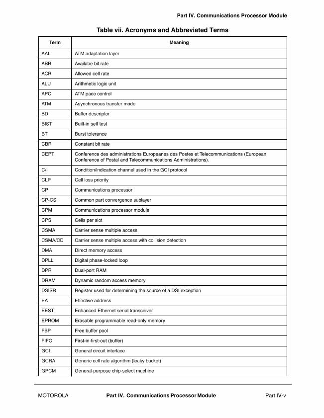
Part IV. Communications Processor Module
Table vii. Acronyms and Abbreviated Terms
Term Meaning
AAL ATM adaptation layer
ABR Availabe bit rate
ACR Allowed cell rate
ALU Arithmetic logic unit
APC ATM pace control
ATM Asynchronous transfer mode
BD Buffer descriptor
BIST Built-in self test
BT Burst tolerance
CBR Constant bit rate
CEPT Conference des administrations Europeanes des Postes et Telecommunications (European Conference of Postal and Telecommunications Administrations).
C/I Condition/indication channel used in the GCI protocol
CLP Cell loss priority
CP Communications processor
CP-CS Common part convergence sublayer
CPM Communications processor module
CPS Cells per slot
CSMA Carrier sense multiple access
CSMA/CD Carrier sense multiple access with collision detection
DMA Direct memory access
DPLL Digital phase-locked loop
DPR Dual-port RAM
DRAM Dynamic random access memory
DSISR Register used for determining the source of a DSI exception
EA Effective address
EEST Enhanced Ethernet serial transceiver
EPROM Erasable programmable read-only memory
FBP Free buffer pool
FIFO First-in-Þrst-out (buffer)
GCI General circuit interface
GCRA Generic cell rate algorithm (leaky bucket)
GPCM General-purpose chip-select machine
MOTOROLA Part IV. Communications Processor Module Part IV-v
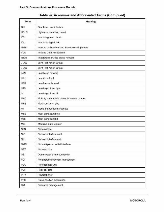
Part IV. Communications Processor Module
GUI Graphical user interface
HDLC High-level data link control
I2C Inter-integrated circuit
IDL Inter-chip digital link
IEEE Institute of Electrical and Electronics Engineers
IrDA Infrared Data Association
ISDN Integrated services digital network
JTAG Joint Test Action Group
JTAG Joint Test Action Group
LAN Local area network
LIFO Last-in-Þrst-out
LRU Least recently used
LSB Least-signiÞcant byte
lsb Least-signiÞcant bit
MAC Multiply accumulate or media access control
MBS Maximum burst size
MII Media-independent interface
MSB Most-signiÞcant byte
msb Most-signiÞcant bit
MSR Machine state register
NaN Not a number
NIC Network interface card
NIU Network interface unit
NMSI Nonmultiplexed serial interface
NRT Non-real time
OSI Open systems interconnection
PCI Peripheral component interconnect
PDU Protocol data unit
PCR Peak cell rate
PHY Physical layer
PPM Pulse-position modulation
RM Resource management
Table vii. Acronyms and Abbreviated Terms (Continued)
Term Meaning
Part IV-vi MOTOROLA
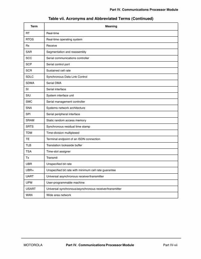
Part IV. Communications Processor Module
RT Real-time
RTOS Real-time operating system
Rx Receive
SAR Segmentation and reassembly
SCC Serial communications controller
SCP Serial control port
SCR Sustained cell rate
SDLC Synchronous Data Link Control
SDMA Serial DMA
SI Serial interface
SIU System interface unit
SMC Serial management controller
SNA Systems network architecture
SPI Serial peripheral interface
SRAM Static random access memory
SRTS Synchronous residual time stamp
TDM Time-division multiplexed
TE Terminal endpoint of an ISDN connection
TLB Translation lookaside buffer
TSA Time-slot assigner
Tx Transmit
UBR UnspeciÞed bit rate
UBR+ UnspeciÞed bit rate with minimum cell rate guarantee
UART Universal asynchronous receiver/transmitter
UPM User-programmable machine
USART Universal synchronous/asynchronous receiver/transmitter
WAN Wide area network
Table vii. Acronyms and Abbreviated Terms (Continued)
Term Meaning
MOTOROLA Part IV. Communications Processor Module Part IV-vii
Part IV. Communications Processor Module
Part IV-viii MOTOROLA
Chapter 13 Communications Processor Module Overview130130
The MPC8260Õs communications processor module (CPM) is a superset of the MPC860PowerQUICC CPM, with enhancements in performance and the addition of hardware andmicrocode routines for supporting high bit-rate protocols like ATM and Fast Ethernet. Thesupport for multiple HDLC channels is enhanced to support up to 256 HDLC channels.
13.1 FeaturesThe CPM includes various blocks to provide the system with an efÞcient way to handle datacommunication tasks. The following is a list of the CPMÕs important features.
¥ Communications processor (CP)
Ñ One instruction per clock
Ñ Executes code from internal ROM or dual-port RAM
Ñ 32-bit RISC architecture
Ñ Tuned for communication environments: instruction set supports CRC computation and bit manipulation.
Ñ Internal timer
Ñ Interfaces with the PowerPCª embedded core processor through a 24-Kbyte dual-port RAM and virtual DMA channels for each peripheral controller
Ñ Handles serial protocols and virtual DMA.
¥ Three full-duplex fast serial communications controllers (FCCs) support the following protocols:
Ñ ATM protocol through UTOPIA interface (FCC1 and FCC2 only)
Ñ IEEE802.3/Fast Ethernet
Ñ HDLC
Ñ Totally transparent operation
¥ Two multi-channel controllers (MCCs) that together can handle up to 256 HDLC/transparent channels at 64 Kbps each, multiplexed on up to eight TDM interfaces
MOTOROLA Chapter 13. Communications Processor Module Overview 13-1
Part IV. Communications Processor Module
¥ Four full-duplex serial communications controllers (SCCs) support the following protocols:
Ñ IEEE802.3/Ethernet
Ñ High level/synchronous data link control (HDLC/SDLC)
Ñ LocalTalk (HDLC-based local area network protocol)
Ñ Universal asynchronous receiver transmitter (UART)
Ñ Synchronous UART (1x clock mode)
Ñ Binary synchronous communication (BISYNC)
Ñ Totally transparent operation
¥ Two full-duplex serial management controllers (SMCs) support the following protocols:
Ñ GCI (ISDN interface) monitor and C/I channels
Ñ UART
Ñ Transparent operation
¥ Serial peripheral interface (SPI) support for master or slave
¥ I2C bus controller
¥ Time-slot assigner supports multiplexing of data from any of the SCCs, FCCs, SMCs, and MCCs onto eight time-division multiplexed (TDM) interfaces. The time-slot assigner supports the following TDM formats:
Ñ T1/CEPT lines
Ñ T3/E3
Ñ Pulse code modulation (PCM) highway interface
Ñ ISDN primary rate
Ñ Motorola interchip digital link (IDL)
Ñ General circuit interface (GCI)
Ñ User-deÞned interfaces
¥ Eight independent baud rate generators (BRGs)
¥ Four general-purpose 16-bit timers or two 32-bit timers
¥ General-purpose parallel portsÑsixteen parallel I/O lines with interrupt capability
Figure 13-1 shows the MPC8260Õs CPM block diagram.
13-2 MPC8260 PowerQUICC II UserÕs Manual MOTOROLA
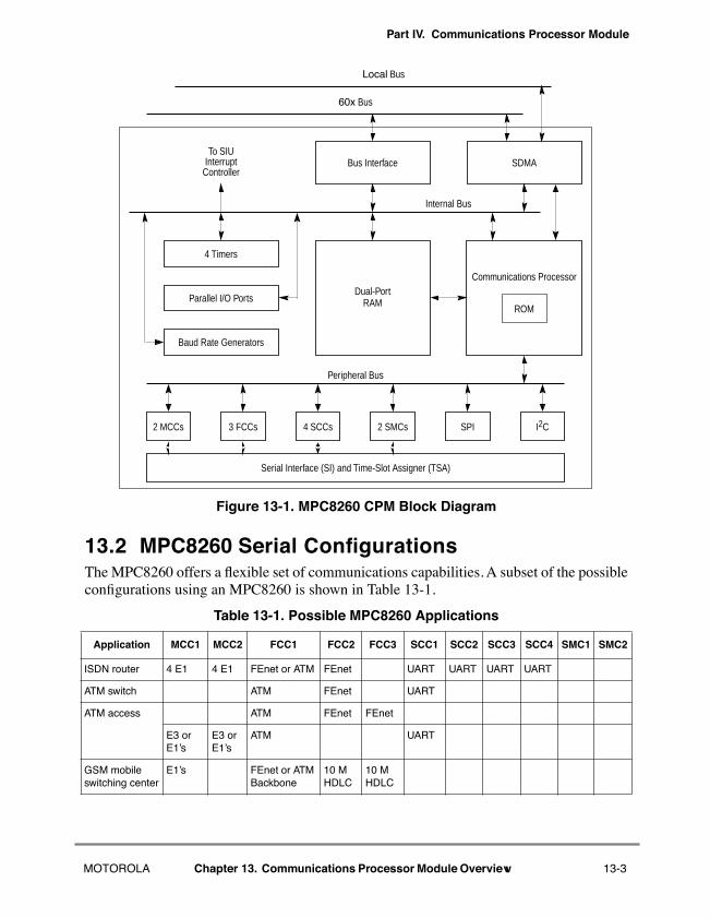
Part IV. Communications Processor Module
Figure 13-1. MPC8260 CPM Block Diagram
13.2 MPC8260 Serial ConÞgurationsThe MPC8260 offers a ßexible set of communications capabilities. A subset of the possibleconÞgurations using an MPC8260 is shown in Table 13-1.
Table 13-1. Possible MPC8260 Applications
Application MCC1 MCC2 FCC1 FCC2 FCC3 SCC1 SCC2 SCC3 SCC4 SMC1 SMC2
ISDN router 4 E1 4 E1 FEnet or ATM FEnet UART UART UART UART
ATM switch ATM FEnet UART
ATM access ATM FEnet FEnet
E3 or E1Õs
E3 or E1Õs
ATM UART
GSM mobile switching center
E1Õs FEnet or ATM Backbone
10 M HDLC
10 M HDLC
Baud Rate Generators
60x Bus
2 MCCs 3 FCCs 4 SCCs 2 SMCs SPI I2C
To SIU
4 Timers
Parallel I/O Ports
Bus Interface SDMA
Dual-PortRAM
Communications Processor
ROM
Internal Bus
Peripheral Bus
Serial Interface (SI) and Time-Slot Assigner (TSA)
InterruptController
Local Bus
MOTOROLA Chapter 13. Communications Processor Module Overview 13-3
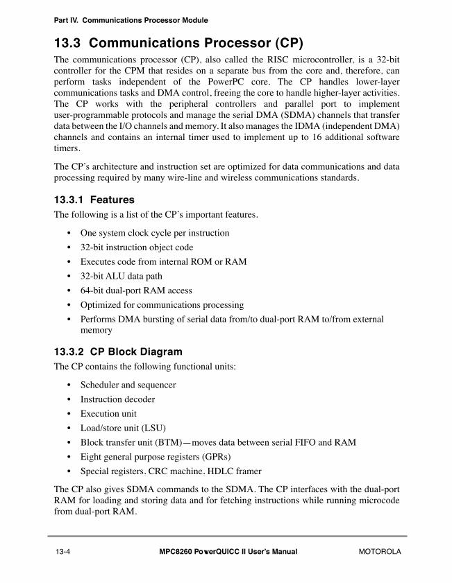
Part IV. Communications Processor Module
13.3 Communications Processor (CP) The communications processor (CP), also called the RISC microcontroller, is a 32-bitcontroller for the CPM that resides on a separate bus from the core and, therefore, canperform tasks independent of the PowerPC core. The CP handles lower-layercommunications tasks and DMA control, freeing the core to handle higher-layer activities.The CP works with the peripheral controllers and parallel port to implementuser-programmable protocols and manage the serial DMA (SDMA) channels that transferdata between the I/O channels and memory. It also manages the IDMA (independent DMA)channels and contains an internal timer used to implement up to 16 additional softwaretimers.
The CPÕs architecture and instruction set are optimized for data communications and dataprocessing required by many wire-line and wireless communications standards.
13.3.1 FeaturesThe following is a list of the CPÕs important features.
¥ One system clock cycle per instruction
¥ 32-bit instruction object code
¥ Executes code from internal ROM or RAM
¥ 32-bit ALU data path
¥ 64-bit dual-port RAM access
¥ Optimized for communications processing
¥ Performs DMA bursting of serial data from/to dual-port RAM to/from external memory
13.3.2 CP Block DiagramThe CP contains the following functional units:
¥ Scheduler and sequencer
¥ Instruction decoder
¥ Execution unit
¥ Load/store unit (LSU)
¥ Block transfer unit (BTM)Ñmoves data between serial FIFO and RAM
¥ Eight general purpose registers (GPRs)
¥ Special registers, CRC machine, HDLC framer
The CP also gives SDMA commands to the SDMA. The CP interfaces with the dual-portRAM for loading and storing data and for fetching instructions while running microcodefrom dual-port RAM.
13-4 MPC8260 PowerQUICC II UserÕs Manual MOTOROLA
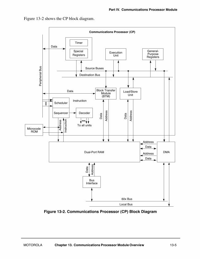
Part IV. Communications Processor Module
Figure 13-2 shows the CP block diagram.
Figure 13-2. Communications Processor (CP) Block Diagram
General-
Load/StoreUnit
Block Transfer
Dual-Port RAM
Microcode
DMA
Execution
Source Buses
Destination Bus
Address
Data
Address
Data
Add
ress
Dat
a
Per
iphe
rial B
us
Scheduler
Decoder
Instruction
To all units
Bus
Communications Processor (CP)
Timer
Special
Sequencer
Registers Unit
Data
Add
ress
Dat
a
Data
ROM Inst
ruct
ion
Add
ress
Add
ress
Dat
a
Interface
Local Bus
60x Bus
Module(BTM)
PurposeRegisters
MOTOROLA Chapter 13. Communications Processor Module Overview 13-5
Part IV. Communications Processor Module
13.3.3 PowerPC Core InterfaceThe CP communicates with the PowerPC core in several ways:
¥ Many parameters are exchanged through the dual-port RAM.
¥ The CP can execute special commands issued by the core. These commands should only be issued in special situations like exceptions or error recovery.
¥ The CP generates interrupts through the SIU interrupt controller.
¥ The PowerPC core can read the CPM status/event registers at any time.
13.3.4 Peripheral InterfaceThe CP uses the peripheral bus to communicate with all of its peripherals. Each FCC andeach SCC has a separate receive and transmit FIFOs. The FCC FIFOs are 192 bytes. TheSCC FIFOs are 32 bytes. The SMCs, SPI, and I2C are all double-buffered, creating effectiveFIFO sizes of two characters.
Table 13-2 shows the order in which the CP handles requests from peripherals from highestto lowest priority.
Table 13-2. Peripheral Prioritization
Priority Request
1 Reset in the CPCR or SRESET
2 SDMA bus error
3 Commands issued to the CPCR
4 Emergency (from FCCs, MCCs, and SCCs)
5 IDMA[1Ð4] emulation (defaultÑoption 1)1
6 FCC1 receive
7 FCC1 transmit
8 MCC1 receive
9 MCC2 receive
10 MCC1 transmit
11 MCC2 transmit
12 FCC2 receive
13 FCC2 transmit
14 FCC3 receive
15 FCC3 transmit
16 SCC1 receive
17 SCC1 transmit
18 SCC2 receive
13-6 MPC8260 PowerQUICC II UserÕs Manual MOTOROLA
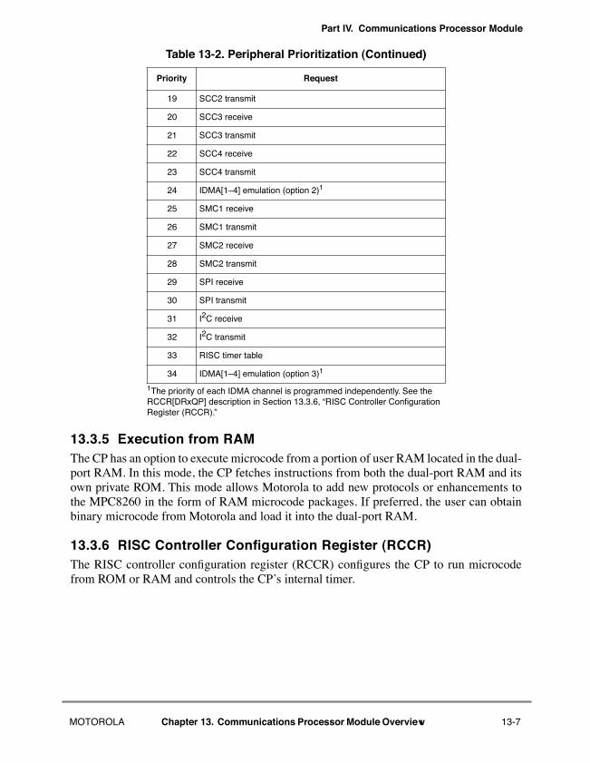
Part IV. Communications Processor Module
13.3.5 Execution from RAMThe CP has an option to execute microcode from a portion of user RAM located in the dual-port RAM. In this mode, the CP fetches instructions from both the dual-port RAM and itsown private ROM. This mode allows Motorola to add new protocols or enhancements tothe MPC8260 in the form of RAM microcode packages. If preferred, the user can obtainbinary microcode from Motorola and load it into the dual-port RAM.
13.3.6 RISC Controller ConÞguration Register (RCCR)The RISC controller conÞguration register (RCCR) conÞgures the CP to run microcodefrom ROM or RAM and controls the CPÕs internal timer.
19 SCC2 transmit
20 SCC3 receive
21 SCC3 transmit
22 SCC4 receive
23 SCC4 transmit
24 IDMA[1Ð4] emulation (option 2)1
25 SMC1 receive
26 SMC1 transmit
27 SMC2 receive
28 SMC2 transmit
29 SPI receive
30 SPI transmit
31 I2C receive
32 I2C transmit
33 RISC timer table
34 IDMA[1Ð4] emulation (option 3)1
1The priority of each IDMA channel is programmed independently. See the RCCR[DRxQP] description in Section 13.3.6, ÒRISC Controller ConÞguration Register (RCCR).Ó
Table 13-2. Peripheral Prioritization (Continued)
Priority Request
MOTOROLA Chapter 13. Communications Processor Module Overview 13-7
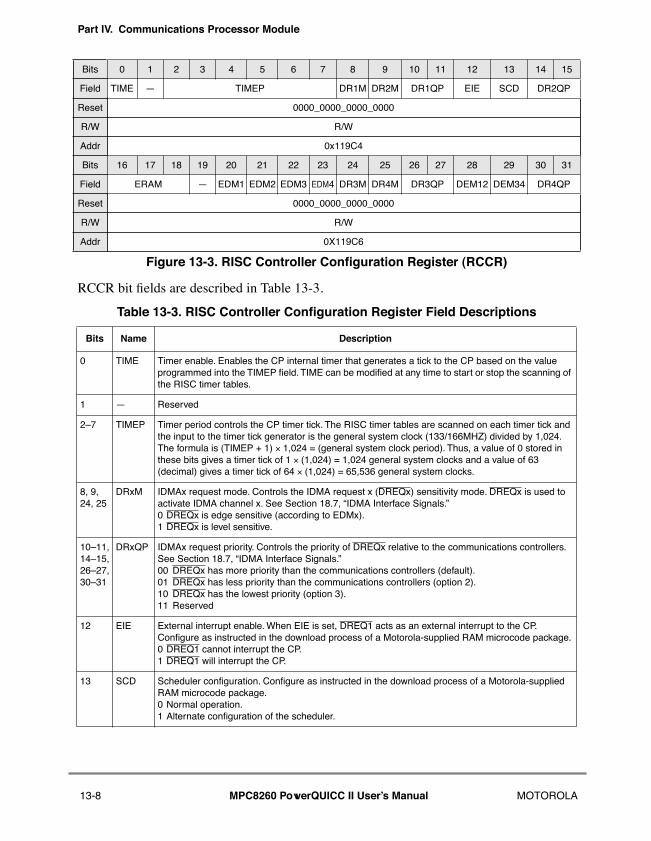
Part IV. Communications Processor Module
RCCR bit Þelds are described in Table 13-3.
Bits 0 1 2 3 4 5 6 7 8 9 10 11 12 13 14 15
Field TIME Ñ TIMEP DR1M DR2M DR1QP EIE SCD DR2QP
Reset 0000_0000_0000_0000
R/W R/W
Addr 0x119C4
Bits 16 17 18 19 20 21 22 23 24 25 26 27 28 29 30 31
Field ERAM Ñ EDM1 EDM2 EDM3 EDM4 DR3M DR4M DR3QP DEM12 DEM34 DR4QP
Reset 0000_0000_0000_0000
R/W R/W
Addr 0X119C6
Figure 13-3. RISC Controller Configuration Register (RCCR)
Table 13-3. RISC Controller Configuration Register Field Descriptions
Bits Name Description
0 TIME Timer enable. Enables the CP internal timer that generates a tick to the CP based on the value programmed into the TIMEP Þeld. TIME can be modiÞed at any time to start or stop the scanning of the RISC timer tables.
1 Ñ Reserved
2Ð7 TIMEP Timer period controls the CP timer tick. The RISC timer tables are scanned on each timer tick and the input to the timer tick generator is the general system clock (133/166MHZ) divided by 1,024. The formula is (TIMEP + 1) ´ 1,024 = (general system clock period). Thus, a value of 0 stored in these bits gives a timer tick of 1 ´ (1,024) = 1,024 general system clocks and a value of 63 (decimal) gives a timer tick of 64 ´ (1,024) = 65,536 general system clocks.
8, 9,24, 25
DRxM IDMAx request mode. Controls the IDMA request x (DREQx) sensitivity mode. DREQx is used to activate IDMA channel x. See Section 18.7, ÒIDMA Interface Signals.Ó0 DREQx is edge sensitive (according to EDMx).1 DREQx is level sensitive.
10Ð11,14Ð15,26Ð27,30Ð31
DRxQP IDMAx request priority. Controls the priority of DREQx relative to the communications controllers. See Section 18.7, ÒIDMA Interface Signals.Ó00 DREQx has more priority than the communications controllers (default).01 DREQx has less priority than the communications controllers (option 2).10 DREQx has the lowest priority (option 3).11 Reserved
12 EIE External interrupt enable. When EIE is set, DREQ1 acts as an external interrupt to the CP. ConÞgure as instructed in the download process of a Motorola-supplied RAM microcode package.0 DREQ1 cannot interrupt the CP.1 DREQ1 will interrupt the CP.
13 SCD Scheduler conÞguration. ConÞgure as instructed in the download process of a Motorola-supplied RAM microcode package.0 Normal operation.1 Alternate conÞguration of the scheduler.
13-8 MPC8260 PowerQUICC II UserÕs Manual MOTOROLA
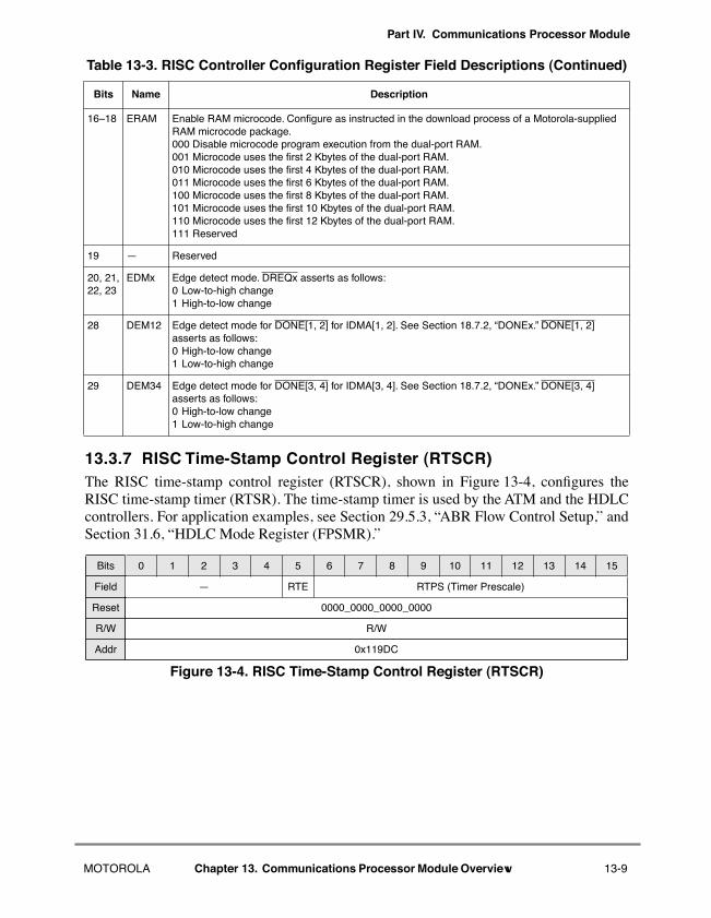
Part IV. Communications Processor Module
13.3.7 RISC Time-Stamp Control Register (RTSCR)The RISC time-stamp control register (RTSCR), shown in Figure 13-4, conÞgures theRISC time-stamp timer (RTSR). The time-stamp timer is used by the ATM and the HDLCcontrollers. For application examples, see Section 29.5.3, ÒABR Flow Control Setup,Ó andSection 31.6, ÒHDLC Mode Register (FPSMR).Ó
16Ð18 ERAM Enable RAM microcode. ConÞgure as instructed in the download process of a Motorola-supplied RAM microcode package. 000 Disable microcode program execution from the dual-port RAM.001 Microcode uses the Þrst 2 Kbytes of the dual-port RAM.010 Microcode uses the Þrst 4 Kbytes of the dual-port RAM.011 Microcode uses the Þrst 6 Kbytes of the dual-port RAM.100 Microcode uses the Þrst 8 Kbytes of the dual-port RAM.101 Microcode uses the Þrst 10 Kbytes of the dual-port RAM.110 Microcode uses the Þrst 12 Kbytes of the dual-port RAM.111 Reserved
19 Ñ Reserved
20, 21,22, 23
EDMx Edge detect mode. DREQx asserts as follows:0 Low-to-high change1 High-to-low change
28 DEM12 Edge detect mode for DONE[1, 2] for IDMA[1, 2]. See Section 18.7.2, ÒDONEx.Ó DONE[1, 2] asserts as follows:0 High-to-low change1 Low-to-high change
29 DEM34 Edge detect mode for DONE[3, 4] for IDMA[3, 4]. See Section 18.7.2, ÒDONEx.Ó DONE[3, 4] asserts as follows:0 High-to-low change1 Low-to-high change
Bits 0 1 2 3 4 5 6 7 8 9 10 11 12 13 14 15
Field Ñ RTE RTPS (Timer Prescale)
Reset 0000_0000_0000_0000
R/W R/W
Addr 0x119DC
Figure 13-4. RISC Time-Stamp Control Register (RTSCR)
Table 13-3. RISC Controller Configuration Register Field Descriptions (Continued)
Bits Name Description
MOTOROLA Chapter 13. Communications Processor Module Overview 13-9
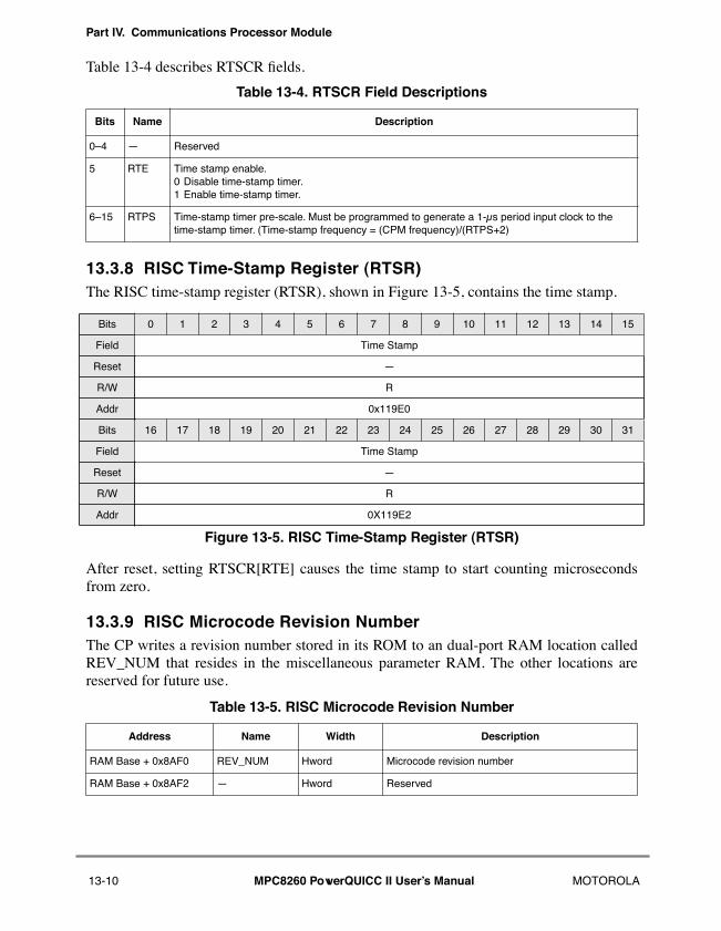
Part IV. Communications Processor Module
Table 13-4 describes RTSCR Þelds.
13.3.8 RISC Time-Stamp Register (RTSR)The RISC time-stamp register (RTSR), shown in Figure 13-5, contains the time stamp.
After reset, setting RTSCR[RTE] causes the time stamp to start counting microsecondsfrom zero.
13.3.9 RISC Microcode Revision NumberThe CP writes a revision number stored in its ROM to an dual-port RAM location calledREV_NUM that resides in the miscellaneous parameter RAM. The other locations arereserved for future use.
Table 13-4. RTSCR Field Descriptions
Bits Name Description
0Ð4 Ñ Reserved
5 RTE Time stamp enable.0 Disable time-stamp timer.1 Enable time-stamp timer.
6Ð15 RTPS Time-stamp timer pre-scale. Must be programmed to generate a 1-µs period input clock to the time-stamp timer. (Time-stamp frequency = (CPM frequency)/(RTPS+2)
Bits 0 1 2 3 4 5 6 7 8 9 10 11 12 13 14 15
Field Time Stamp
Reset Ñ
R/W R
Addr 0x119E0
Bits 16 17 18 19 20 21 22 23 24 25 26 27 28 29 30 31
Field Time Stamp
Reset Ñ
R/W R
Addr 0X119E2
Figure 13-5. RISC Time-Stamp Register (RTSR)
Table 13-5. RISC Microcode Revision Number
Address Name Width Description
RAM Base + 0x8AF0 REV_NUM Hword Microcode revision number
RAM Base + 0x8AF2 Ñ Hword Reserved
13-10 MPC8260 PowerQUICC II UserÕs Manual MOTOROLA
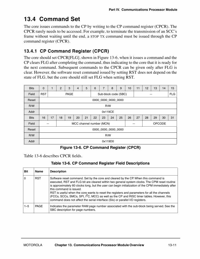
Part IV. Communications Processor Module
13.4 Command SetThe core issues commands to the CP by writing to the CP command register (CPCR). TheCPCR rarely needs to be accessed. For example, to terminate the transmission of an SCCÕsframe without waiting until the end, a STOP TX command must be issued through the CPcommand register (CPCR).
13.4.1 CP Command Register (CPCR)The core should set CPCR[FLG], shown in Figure 13-6, when it issues a command and theCP clears FLG after completing the command, thus indicating to the core that it is ready forthe next command. Subsequent commands to the CPCR can be given only after FLG isclear. However, the software reset command issued by setting RST does not depend on thestate of FLG, but the core should still set FLG when setting RST.
Table 13-6 describes CPCR Þelds.
Bits 0 1 2 3 4 5 6 7 8 9 10 11 12 13 14 15
Field RST PAGE Sub-block code (SBC) Ñ FLG
Reset 0000_0000_0000_0000
R/W R/W
Addr 0x119CE
Bits 16 17 18 19 20 21 22 23 24 25 26 27 28 29 30 31
Field Ñ MCC channel number (MCN) Ñ OPCODE
Reset 0000_0000_0000_0000
R/W R/W
Addr 0x119D0
Figure 13-6. CP Command Register (CPCR)
Table 13-6. CP Command Register Field Descriptions
Bit Name Description
0 RST Software reset command. Set by the core and cleared by the CP. When this command is executed, RST and FLG bit are cleared within two general system clocks. The CPM reset routine is approximately 60 clocks long, but the user can begin initialization of the CPM immediately after this command is issued. RST is useful when the core wants to reset the registers and parameters for all the channels (FCCs, SCCs, SMCs, SPI, I2C, MCC) as well as the CP and RISC timer tables. However, this command does not affect the serial interface (SIx) or parallel I/O registers.
1Ð5 PAGE Indicates the parameter RAM page number associated with the sub-block being served. See the SBC description for page numbers.
MOTOROLA Chapter 13. Communications Processor Module Overview 13-11
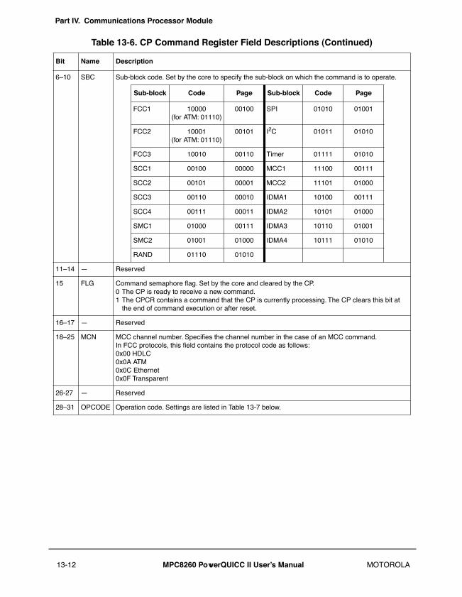
Part IV. Communications Processor Module
6Ð10 SBC Sub-block code. Set by the core to specify the sub-block on which the command is to operate.
Sub-block Code Page Sub-block Code Page
FCC1 10000(for ATM: 01110)
00100 SPI 01010 01001
FCC2 10001(for ATM: 01110)
00101 I2C 01011 01010
FCC3 10010 00110 Timer 01111 01010
SCC1 00100 00000 MCC1 11100 00111
SCC2 00101 00001 MCC2 11101 01000
SCC3 00110 00010 IDMA1 10100 00111
SCC4 00111 00011 IDMA2 10101 01000
SMC1 01000 00111 IDMA3 10110 01001
SMC2 01001 01000 IDMA4 10111 01010
RAND 01110 01010
11Ð14 Ñ Reserved
15 FLG Command semaphore ßag. Set by the core and cleared by the CP.0 The CP is ready to receive a new command.1 The CPCR contains a command that the CP is currently processing. The CP clears this bit at
the end of command execution or after reset.
16Ð17 Ñ Reserved
18Ð25 MCN MCC channel number. SpeciÞes the channel number in the case of an MCC command.In FCC protocols, this Þeld contains the protocol code as follows:0x00 HDLC0x0A ATM0x0C Ethernet0x0F Transparent
26-27 Ñ Reserved
28Ð31 OPCODE Operation code. Settings are listed in Table 13-7 below.
Table 13-6. CP Command Register Field Descriptions (Continued)
Bit Name Description
13-12 MPC8260 PowerQUICC II UserÕs Manual MOTOROLA
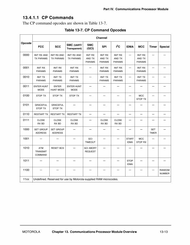
Part IV. Communications Processor Module
13.4.1.1 CP CommandsThe CP command opcodes are shown in Table 13-7.
Table 13-7. CP Command Opcodes
Opcode
Channel
FCC SCCSMC (UART/Transparent)
SMC (GCI)
SPI I2C IDMA MCC Timer Special
0000 INIT RX AND TX PARAMS
INIT RX AND TX PARAMS
INIT RX AND TX PARAMS
INIT RX AND TX PARAMS
INIT RX AND TX PARAMS
INIT RX AND TX PARAMS
Ñ INIT RX AND TX PARAMS
Ñ Ñ
0001 INIT RX PARAMS
INIT RX PARAMS
INIT RX PARAMS
Ñ INIT RX PARAMS
INIT RX PARAMS
Ñ INIT RX PARAMS
Ñ Ñ
0010 INIT TX PARAMS
INIT TX PARAMS
INIT TX PARAMS
Ñ INIT TX PARAMS
INIT TX PARAMS
Ñ INIT TX PARAMS
Ñ Ñ
0011 ENTER HUNT MODE
ENTER HUNT MODE
ENTER HUNT MODE
Ñ Ñ Ñ Ñ Ñ Ñ Ñ
0100 STOP TX STOP TX STOP TX Ñ Ñ Ñ Ñ MCC STOP TX
Ñ Ñ
0101 GRACEFUL
STOP TX
GRACEFUL
STOP TX
Ñ Ñ Ñ Ñ Ñ Ñ Ñ Ñ
0110 RESTART TX RESTART TX RESTART TX Ñ Ñ Ñ Ñ Ñ Ñ Ñ
0111 CLOSE
RX BD
CLOSE
RX BD
CLOSE
RX BD
Ñ CLOSE
RX BD
CLOSE
RX BD
Ñ Ñ Ñ Ñ
1000 SET GROUP
ADDRESS
SET GROUP
ADDRESS
Ñ Ñ Ñ Ñ Ñ Ñ SET
TIMER
Ñ
1001 Ñ Ñ Ñ GCI TIMEOUT
Ñ Ñ START IDMA
MCC STOP RX
Ñ Ñ
1010 ATM TRANSMIT COMMAND
RESET BCS Ñ GCI ABORT
REQUEST
Ñ Ñ Ñ Ñ Ñ Ñ
1011 Ñ Ñ Ñ Ñ Ñ Ñ STOP IDMA
Ñ Ñ Ñ
1100 Ñ Ñ Ñ Ñ Ñ Ñ Ñ Ñ Ñ RANDOM NUMBER
11XX UndeÞned. Reserved for use by Motorola-supplied RAM microcodes.
MOTOROLA Chapter 13. Communications Processor Module Overview 13-13
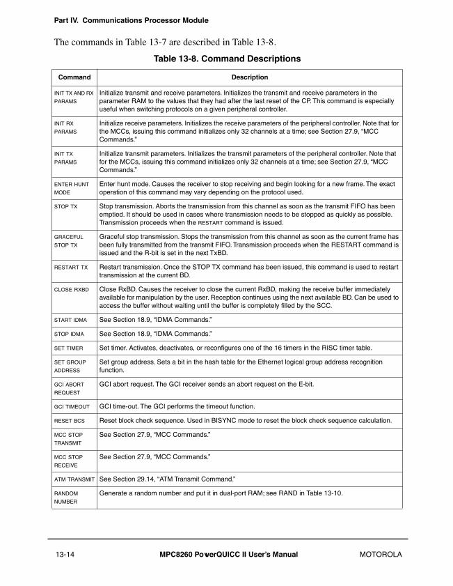
Part IV. Communications Processor Module
The commands in Table 13-7 are described in Table 13-8.
Table 13-8. Command Descriptions
Command Description
INIT TX AND RX PARAMS
Initialize transmit and receive parameters. Initializes the transmit and receive parameters in the parameter RAM to the values that they had after the last reset of the CP. This command is especially useful when switching protocols on a given peripheral controller.
INIT RX PARAMS
Initialize receive parameters. Initializes the receive parameters of the peripheral controller. Note that for the MCCs, issuing this command initializes only 32 channels at a time; see Section 27.9, ÒMCC Commands.Ó
INIT TX PARAMS
Initialize transmit parameters. Initializes the transmit parameters of the peripheral controller. Note that for the MCCs, issuing this command initializes only 32 channels at a time; see Section 27.9, ÒMCC Commands.Ó
ENTER HUNT MODE
Enter hunt mode. Causes the receiver to stop receiving and begin looking for a new frame. The exact operation of this command may vary depending on the protocol used.
STOP TX Stop transmission. Aborts the transmission from this channel as soon as the transmit FIFO has been emptied. It should be used in cases where transmission needs to be stopped as quickly as possible. Transmission proceeds when the RESTART command is issued.
GRACEFUL STOP TX
Graceful stop transmission. Stops the transmission from this channel as soon as the current frame has been fully transmitted from the transmit FIFO. Transmission proceeds when the RESTART command is issued and the R-bit is set in the next TxBD.
RESTART TX Restart transmission. Once the STOP TX command has been issued, this command is used to restart transmission at the current BD.
CLOSE RXBD Close RxBD. Causes the receiver to close the current RxBD, making the receive buffer immediately available for manipulation by the user. Reception continues using the next available BD. Can be used to access the buffer without waiting until the buffer is completely Þlled by the SCC.
START IDMA See Section 18.9, ÒIDMA Commands.Ó
STOP IDMA See Section 18.9, ÒIDMA Commands.Ó
SET TIMER Set timer. Activates, deactivates, or reconÞgures one of the 16 timers in the RISC timer table.
SET GROUP ADDRESS
Set group address. Sets a bit in the hash table for the Ethernet logical group address recognition function.
GCI ABORT REQUEST
GCI abort request. The GCI receiver sends an abort request on the E-bit.
GCI TIMEOUT GCI time-out. The GCI performs the timeout function.
RESET BCS Reset block check sequence. Used in BISYNC mode to reset the block check sequence calculation.
MCC STOP TRANSMIT
See Section 27.9, ÒMCC Commands.Ó
MCC STOP RECEIVE
See Section 27.9, ÒMCC Commands.Ó
ATM TRANSMIT See Section 29.14, ÒATM Transmit Command.Ó
RANDOM NUMBER
Generate a random number and put it in dual-port RAM; see RAND in Table 13-10.
13-14 MPC8260 PowerQUICC II UserÕs Manual MOTOROLA
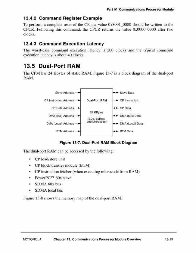
Part IV. Communications Processor Module
13.4.2 Command Register ExampleTo perform a complete reset of the CP, the value 0x8001_0000 should be written to theCPCR. Following this command, the CPCR returns the value 0x0000_0000 after twoclocks.
13.4.3 Command Execution LatencyThe worst-case command execution latency is 200 clocks and the typical commandexecution latency is about 40 clocks.
13.5 Dual-Port RAM The CPM has 24 Kbytes of static RAM. Figure 13-7 is a block diagram of the dual-portRAM.
Figure 13-7. Dual-Port RAM Block Diagram
The dual-port RAM can be accessed by the following:
¥ CP load/store unit
¥ CP block transfer module (BTM)
¥ CP instruction fetcher (when executing microcode from RAM)
¥ PowerPCª 60x slave
¥ SDMA 60x bus
¥ SDMA local bus
Figure 13-8 shows the memory map of the dual-port RAM.
Slave Address
CP Instruction Address
CP Data Address
24 KBytes
Dual-Port RAM
(BDs, Buffersand Microcode)
DMA (60x) Address
DMA (Local) Address
BTM Address
Slave Data
CP Instruction
CP Data
DMA (60x) Data
DMA (Local) Data
BTM Data
MOTOROLA Chapter 13. Communications Processor Module Overview 13-15
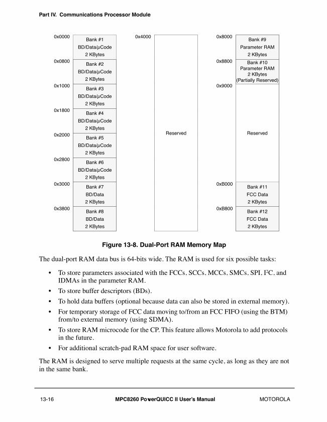
Part IV. Communications Processor Module
Figure 13-8. Dual-Port RAM Memory Map
The dual-port RAM data bus is 64-bits wide. The RAM is used for six possible tasks:
¥ To store parameters associated with the FCCs, SCCs, MCCs, SMCs, SPI, I2C, and IDMAs in the parameter RAM.
¥ To store buffer descriptors (BDs).
¥ To hold data buffers (optional because data can also be stored in external memory).
¥ For temporary storage of FCC data moving to/from an FCC FIFO (using the BTM) from/to external memory (using SDMA).
¥ To store RAM microcode for the CP. This feature allows Motorola to add protocols in the future.
¥ For additional scratch-pad RAM space for user software.
The RAM is designed to serve multiple requests at the same cycle, as long as they are notin the same bank.
BD/Data/µCode
2 KBytes
Bank #10x0000
BD/Data/µCode
2 KBytes
Bank #20x0800
BD/Data/µCode
2 KBytes
Bank #30x1000
BD/Data/µCode
2 KBytes
Bank #40x1800
BD/Data/µCode
2 KBytes
Bank #50x2000
BD/Data/µCode
2 KBytes
Bank #60x2800
BD/Data
2 KBytes
Bank #70x3000
BD/Data
2 KBytes
Bank #80x3800
BD/Data/µCode
2 KBytes
Bank #10x4000
BD/Data/µCode
2 KBytes
Bank #1
BD/Data/µCode
2 KBytes
Bank #1
BD/Data/µCode
2 KBytes
Bank #1
BD/Data/µCode
2 KBytes
Bank #1
BD/Data/µCode
2 KBytes
Bank #1
BD/Data/µCode
2 KBytes
Bank #1
BD/Data/µCode
2 KBytes
Bank #1
Parameter RAM
2 KBytes
Bank #90x8000
Parameter RAM2 KBytes
Bank #100x8800
BD/Data/µCode
2 KBytes
Bank #110x9000
BD/Data/µCode
2 KBytes
Bank #1
BD/Data/µCode
2 KBytes
Bank #1
BD/Data/µCode
2 KBytes
Bank #1
FCC Data
2 KBytes
Bank #110xB000
FCC Data
2 KBytes
Bank #120xB800
Reserved Reserved
(Partially Reserved)
13-16 MPC8260 PowerQUICC II UserÕs Manual MOTOROLA
Part IV. Communications Processor Module
Only the parameters in the parameter RAM and the microcode RAM option require Þxedaddresses to be used. The BDs, buffer data, and scratchpad RAM can be located in the dual-port system RAM or in any unused parameter RAM, such as, in the area made availablewhen a peripheral controller or sub-block is not being used.
Microcode can be executed from the Þrst 12 Kbytes. To ensure an uninterrupted instructionstream (one per cycle), no other agent is allowed to use a RAM bank used by the microcode.Since the Þrst 12 Kbytes are divided to six 2-Kbyte banks, RAM microcode occupies 2, 4,6, 8, 10, or 12 Kbytes of RAM, depending on RCCR[ERAM]; see Section 13.3.6, ÒRISCController ConÞguration Register (RCCR).Ó
13.5.1 Buffer Descriptors (BDs)The peripheral controllers (FCCs, SCCs, SMCs, MCCs, SPI, and I2C) always use BDs forcontrolling buffers and their BD formats are all the same, as shown in Table 13-9.
If the IDMA is used in the buffer chaining or auto-buffer mode, the IDMA channel also usesBDs. They are described in Section 18.3, ÒIDMA Emulation.Ó
13.5.2 Parameter RAMThe CPM maintains a section of RAM called the parameter RAM, which contains manyparameters for the operation of the FCCs, SCCs, SMCs, SPI, I2C, and IDMA channels. Anoverview of the parameter RAM structure is shown in Table 13-10.
The exact deÞnition of the parameter RAM is contained in each protocol subsectiondescribing a device that uses a parameter RAM. For example, the Ethernet parameter RAMis deÞned differently in some locations from the HDLC-speciÞc parameter RAM.
Table 13-9. Buffer Descriptor Format
Address Descriptor
Offset + 0 Status and control
Offset + 2 Data length
Offset + 4 High-order buffer pointer
Offset + 6 Low-order buffer pointer
MOTOROLA Chapter 13. Communications Processor Module Overview 13-17

Part IV. Communications Processor Module
13.6 RISC Timer TablesThe CP can control up to 16 software timers that are separate from the four general-purposetimers and the BRGs in the CPM. These timers are best used in protocols that do not requireextreme precision, but in which it is preferable to free the core from scanning the softwareÕs
Table 13-10. Parameter RAM
Page Address 1
1Offset from RAM_BASE
Peripheral Size (Bytes)
1 0x8000 SCC1 256
2 0x8100 SCC2 256
3 0x8200 SCC3 256
4 0x8300 SCC4 256
5 0x8400 FCC1 256
6 0x8500 FCC2 256
7 0x8600 FCC3 256
8 0x8700 MCC1 128
0x8780 Reserved 124
0x87FC SMC1_BASE 2
0x87FE IDMA1_BASE 2
9 0x8800 MCC2 128
0x8880 Reserved 124
0x88FC SMC2_BASE 2
0x88FE IDMA2_BASE 2
10 0x8900 Reserved 252
0x89FC SPI_BASE 2
0x89FE IDMA3_BASE 2
11 0x8A00 Reserved 224
0x8AE0 RISC Timers 16
0x8AF0 REV_NUM 2
0x8AF2 Reserved 2
0x8AF4 Reserved 4
0x8AF8 RAND 4
0x8AFC I2C_BASE 2
0x8AFE IDMA4_BASE 2
12-16 0x8B00 Reserved 1280
13-18 MPC8260 PowerQUICC II UserÕs Manual MOTOROLA
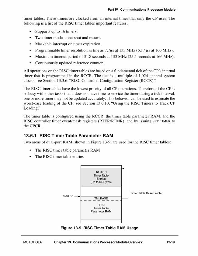
Part IV. Communications Processor Module
timer tables. These timers are clocked from an internal timer that only the CP uses. Thefollowing is a list of the RISC timer tables important features.
¥ Supports up to 16 timers.
¥ Two timer modes: one-shot and restart.
¥ Maskable interrupt on timer expiration.
¥ Programmable timer resolution as Þne as 7.7µs at 133 MHz (6.17 µs at 166 MHz).
¥ Maximum timeout period of 31.8 seconds at 133 MHz (25.5 seconds at 166 MHz).
¥ Continuously updated reference counter.
All operations on the RISC timer tables are based on a fundamental tick of the CPÕs internaltimer that is programmed in the RCCR. The tick is a multiple of 1,024 general systemclocks; see Section 13.3.6, ÒRISC Controller ConÞguration Register (RCCR).Ó
The RISC timer tables have the lowest priority of all CP operations. Therefore, if the CP isso busy with other tasks that it does not have time to service the timer during a tick interval,one or more timer may not be updated accurately. This behavior can be used to estimate theworst-case loading of the CP; see Section 13.6.10, ÒUsing the RISC Timers to Track CPLoading.Ó
The timer table is conÞgured using the RCCR, the timer table parameter RAM, and theRISC controller timer event/mask registers (RTER/RTMR), and by issuing SET TIMER tothe CPCR.
13.6.1 RISC Timer Table Parameter RAMTwo areas of dual-port RAM, shown in Figure 13-9, are used for the RISC timer tables:
¥ The RISC timer table parameter RAM
¥ The RISC timer table entries
Figure 13-9. RISC Timer Table RAM Usage
TM_BASE
16 RISCTimer Table
Entries(Up to 64 Bytes)
RISCTimer Table
Parameter RAM
0x8AE0Timer Table Base Pointer
MOTOROLA Chapter 13. Communications Processor Module Overview 13-19
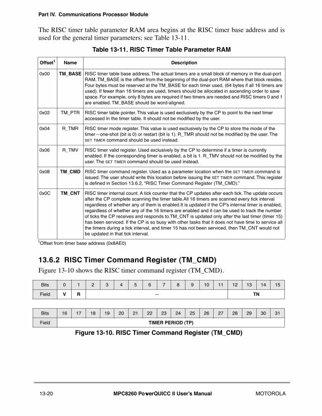
Part IV. Communications Processor Module
The RISC timer table parameter RAM area begins at the RISC timer base address and isused for the general timer parameters; see Table 13-11.
13.6.2 RISC Timer Command Register (TM_CMD)Figure 13-10 shows the RISC timer command register (TM_CMD).
Table 13-11. RISC Timer Table Parameter RAM
Offset1
1Offset from timer base address (0x8AE0)
Name Description
0x00 TM_BASE RISC timer table base address. The actual timers are a small block of memory in the dual-port RAM. TM_BASE is the offset from the beginning of the dual-port RAM where that block resides. Four bytes must be reserved at the TM_BASE for each timer used, (64 bytes if all 16 timers are used). If fewer than 16 timers are used, timers should be allocated in ascending order to save space. For example, only 8 bytes are required if two timers are needed and RISC timers 0 and 1 are enabled. TM_BASE should be word-aligned.
0x02 TM_PTR RISC timer table pointer. This value is used exclusively by the CP to point to the next timer accessed in the timer table. It should not be modiÞed by the user.
0x04 R_TMR RISC timer mode register. This value is used exclusively by the CP to store the mode of the timerÑone-shot (bit is 0) or restart (bit is 1). R_TMR should not be modiÞed by the user. The SET TIMER command should be used instead.
0x06 R_TMV RISC timer valid register. Used exclusively by the CP to determine if a timer is currently enabled. If the corresponding timer is enabled, a bit is 1. R_TMV should not be modiÞed by the user. The SET TIMER command should be used instead.
0x08 TM_CMD RISC timer command register. Used as a parameter location when the SET TIMER command is issued. The user should write this location before issuing the SET TIMER command. This register is deÞned in Section 13.6.2, ÒRISC Timer Command Register (TM_CMD).Ó
0x0C TM_CNT RISC timer internal count. A tick counter that the CP updates after each tick. The update occurs after the CP complete scanning the timer table.All 16 timers are scanned every tick interval regardless of whether any of them is enabled.It is updated if the CPÕs internal timer is enabled, regardless of whether any of the 16 timers are enabled and it can be used to track the number of ticks the CP receives and responds to.TM_CNT is updated only after the last timer (timer 15) has been serviced. If the CP is so busy with other tasks that it does not have time to service all the timers during a tick interval, and timer 15 has not been serviced, then TM_CNT would not be updated in that tick interval.
Bits 0 1 2 3 4 5 6 7 8 9 10 11 12 13 14 15
Field V R Ñ TN
Bits 16 17 18 19 20 21 22 23 24 25 26 27 28 29 30 31
Field TIMER PERIOD (TP)
Figure 13-10. RISC Timer Command Register (TM_CMD)
13-20 MPC8260 PowerQUICC II UserÕs Manual MOTOROLA
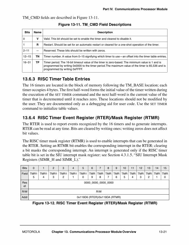
Part IV. Communications Processor Module
TM_CMD Þelds are described in Figure 13-11.
13.6.3 RISC Timer Table EntriesThe 16 timers are located in the block of memory following the TM_BASE location; eachtimer occupies 4 bytes. The Þrst half-word forms the initial value of the timer written duringthe execution of the SET TIMER command and the next half-word is the current value of thetimer that is decremented until it reaches zero. These locations should not be modiÞed bythe user. They are documented only as a debugging aid for user code. Use the SET TIMER
command to initialize table values.
13.6.4 RISC Timer Event Register (RTER)/Mask Register (RTMR)The RTER is used to report events recognized by the 16 timers and to generate interrupts.RTER can be read at any time. Bits are cleared by writing ones; writing zeros does not affectbit values.
The RISC timer mask register (RTMR) is used to enable interrupts that can be generated inthe RTER. Setting an RTMR bit enables the corresponding interrupt in the RTER; clearinga bit masks the corresponding interrupt. An interrupt is generated only if the RISC timertable bit is set in the SIU interrupt mask register; see Section 4.3.1.5, ÒSIU Interrupt MaskRegisters (SIMR_H and SIMR_L).Ó
Figure 13-11. TM_CMD Field Descriptions
Bits Name Description
0 V Valid. This bit should be set to enable the timer and cleared to disable it.
1 R Restart. Should be set for an automatic restart or cleared for a one-shot operation of the timer.
2Ð11 Ñ Reserved. These bits should be written with zeros.
12Ð15 TN Timer number. A value from 0Ð15 signifying which timer to useÑan offset into the timer table entries.
16Ð31 TP Timer period. The 16-bit timeout value of the timer is zero-based. The minimum value is 1 and is programmed by writing 0x0000 to the timer period.The maximum value of the timer is 65,536 and is programmed by writing 0xFFFF.
Bits 0 1 2 3 4 5 6 7 8 9 10 11 12 13 14 15
Field TMR15
TMR14
TMR13
TMR12
TMR11
TMR10
TMR9
TMR8
TMR7
TMR6
TMR5
TMR4
TMR3
TMR2
TMR1
TMR0
Reset
0000_0000_0000_0000
R/W R/W
Addr 0x119D6 (RTER)/0x119DA (RTMR)
Figure 13-12. RISC Timer Event Register (RTER)/Mask Register (RTMR)
MOTOROLA Chapter 13. Communications Processor Module Overview 13-21
Part IV. Communications Processor Module
13.6.5 SET TIMER CommandThe SET TIMER command is used to enable, disable, and conÞgure the 16 timers in the RISCtimer table and is issued to the CPCR. This means the value 0x29E1008 should be writtento CPCR. However, before writing this value, the user should program the TM_CMD Þelds.See Section 13.6.2, ÒRISC Timer Command Register (TM_CMD).Ó
13.6.6 RISC Timer Initialization SequenceThe following sequence initializes the RISC timers:
1. ConÞgure RCCR to determine the preferred tick interval for the entire timer table. The TIME bit is normally set at this time but can be set later if all RISC timers need to be synchronized.
2. Determine the maximum number of timers to be located in the timer table. ConÞgure the TM_BASE in the RISC timer table parameter RAM to point to a location in the dual-port RAM with 4 ´ n bytes available, where n is the number of timers. If n is less than 16, use timer 0 through timer nÐ1 to save space.
3. Clear the TM_CNT Þeld in the RISC timer table parameter RAM to show how many ticks elapsed since the RISC internal timer was enabled. This step is optional.
4. Clear RTER, if it is not already cleared. Write ones to clear this register.
5. ConÞgure RTMR to enable the timers that should generate interrupts. Ones enable interrupts.
6. Set the RISC timer table bit in the SIU interrupt mask register (SIMR_L[RTT]) to generate interrupts to the system. The SIU interrupt controller may require other initialization not mentioned here.
7. ConÞgure the TM_CMD Þeld of the RISC timer table parameter RAM. At this point, determine whether a timer is to be enabled or disabled, one-shot or restart, and what its timeout period should be. If the timer is being disabled, the parameters (other than the timer number) are ignored.
8. Issue the SET TIMER command by writing 0x29E1_0008 to the CPCR.
9. Repeat the preceding two steps for each timer to be enabled or disabled.
13.6.7 RISC Timer Initialization ExampleThe following sequence initializes RISC timer 0 to generate an interrupt approximatelyevery second using a 133-MHz general system clock:
1. Write 111111 to RCCR[TIMEP] to generate the slowest clock. This value generates a tick every 64,512 clocks, which is every 485 µs at 133 MHz.
2. ConÞgure the TM_BASE in the RISC timer table parameter RAM to point to a location in the dual-port RAM with 4 bytes available. Assuming the beginning of dual-port RAM is available, write 0x0000 to TM_BASE.
13-22 MPC8260 PowerQUICC II UserÕs Manual MOTOROLA
Part IV. Communications Processor Module
3. (Optional) Write 0x0000 to the TM_CNT Þeld in the RISC timer table parameter RAM to see how many ticks elapsed since the RISC internal timer was enabled.
4. Write 0xFFFF to the RTER to clear any previous events.
5. Write 0x0001 to the RTMR to enable RISC timer 0 to generate an interrupt.
6. Write 0x0002_0000 to the SIU interrupt mask register (SIMR_L) to allow the RISC timers to generate a system interrupt. Initialize the SIU interrupt conÞguration register.
7. Write 0xC000_080D to the TM_CMD Þeld of the RISC timer table parameter RAM. This enables RISC timer 0 to timeout after 2,061(decimal) ticks of the timer. The timer automatically restarts after it times out.
8. Write 0x29E1_0008 to the CPCR to issue the SET TIMER command.
9. Set RCCR[TIME] to enable the RISC timer to begin operation.
13.6.8 RISC Timer Interrupt HandlingThe following sequence describes what normally would occur within an interrupt handlerfor the RISC timer tables:
1. Once an interrupt occurs, read RTER to see which timers have caused interrupts. The RISC timer event bits are usually cleared by this time.
2. Issue additional SET TIMER commands at this time or later, as preferred. Nothing needs to be done if the timer is being automatically restarted for a repetitive interrupt.
3. Clear the RTT bit in the SIU interrupt pending register (SIPNR_L).
4. Execute the RTE instruction.
13.6.9 RISC Timer Table Scan AlgorithmThe CP scans the timer table once every tick. It handles each of the 16 timers at its turn andchecks for other requests with higher priority to service, before handling the next one. Foreach valid timer in the table, the CP decrements the count and checks for a timeout. If noneoccurs, the CP moves to the next timer. If a timeout occurs, the CP sets the correspondingevent bit in RTER. Then the CP checks to see if the timer is to be restarted and if it is, theCP leaves the timerÕs valid bit set in the R_TMV location and resets the current count to theinitial count. Otherwise, it clears R_TMV. Once the timer table scanning has completed, theCP updates the TM_CNT value in the RISC timer table parameter RAM and stops workingon the timer tables until the next tick.
If a SET TIMER command is issued, the CP makes the appropriate modiÞcations to the timertable and parameter RAM, but does not scan the timer table until the next tick of the internaltimer. It is important to use the SET TIMER command to properly synchronize timer tablemodiÞcations to the execution of the CP.
MOTOROLA Chapter 13. Communications Processor Module Overview 13-23
Part IV. Communications Processor Module
13.6.10 Using the RISC Timers to Track CP LoadingThe RISC timers can be used to track CP loading. The following sequence provides a wayto use the 16 RISC timers to determine if the CP ever exceeds the 96% utilization levelduring any tick interval. Removing the timers adds a 4% margin to the CP utilization level,but the aggressive user can use this technique to push CP performance to its limit. The usershould use the standard initialization sequence and incorporate the following differences:
1. Program the tick of the RISC timers to be every 1,024 x 16 = 16,384 system clocks.
2. Disable RISC timer interrupts, if preferred.
3. Using the SET TIMER command, initialize all 16 RISC timers to have a timer period of 0xFFFF, which equates to 65,536.
4. Program one of the four general-purpose timers to increment once every tick. The general-purpose timer should be free-running and should have a timeout of 65,536.
5. After a few hours of operation, compare the general-purpose timer to the current count of RISC timer 15. If it is more than two ticks different from the general-purpose timer, the CP has, during some tick interval, exceeded the 96% utilization level.
NOTE:General-purpose timers are up counters, but RISC timers aredown counters. The user should take this under considerationwhen comparing timer counts.
13-24 MPC8260 PowerQUICC II UserÕs Manual MOTOROLA
Chapter 14 Serial Interface with Time-Slot Assigner140140
Figure 14-1 shows a block diagram of the TSA. Two SI blocks in the MPC8260 (SI1 andSI2), can be programmed to handle eight TDM lines concurrently with the same ßexibilitydescribed in this manual. TDM channels on SI1 are referred to as TDMa1, TDMb1,TDMc1, TDMd1; TDM channels on SI2 are TDMa2, TDMb2, TDMc2, TDMd2.
MOTOROLA Chapter 14. Serial Interface with Time-Slot Assigner 14-1
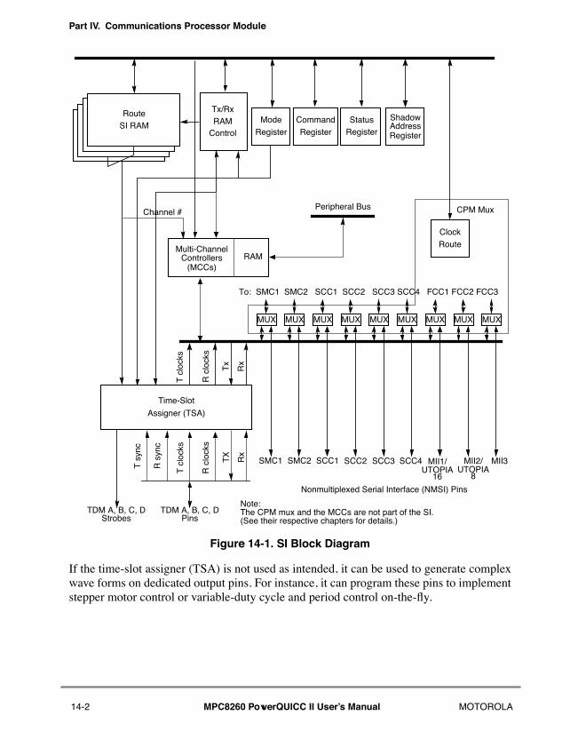
Part IV. Communications Processor Module
Figure 14-1. SI Block Diagram
If the time-slot assigner (TSA) is not used as intended, it can be used to generate complexwave forms on dedicated output pins. For instance, it can program these pins to implementstepper motor control or variable-duty cycle and period control on-the-ßy.
Time-Slot
Assigner (TSA)
R c
lock
s
T c
lock
s
R c
lock
s
T c
lock
s
R s
ync
T s
ync
TDM A, B, C, DPinsStrobes
RouteSI RAM
Tx/RxRAM
Control
Mode
Register
TDM A, B, C, D
Tx
TX
Command
RegisterStatus
Register
SMC1 SMC2 SCC1 SCC2 SCC3 SCC4 MII1/ MII2/
MUX
MII3
To: SMC1 SMC2 SCC1 SCC2 SCC3 SCC4 FCC1 FCC2 FCC3
Multi-Channel
Peripheral Bus
Nonmultiplexed Serial Interface (NMSI) Pins
Channel #
Controllers
Shadow
Register
Clock
RouteRAM
Address
Rx
Rx
UTOPIA UTOPIA16 8
CPM Mux
Note: The CPM mux and the MCCs are not part of the SI.
MUXMUX MUX MUX MUXMUX MUXMUX
(MCCs)
(See their respective chapters for details.)
14-2 MPC8260 PowerQUICC II UserÕs Manual MOTOROLA
Part IV. Communications Processor Module
14.1 FeaturesEach SI has the following features:
¥ Can connect to four independent TDM channels. Each TDM can be one of the following:
Ñ T1 or E1 line
Ñ Integrated services digital network primary rate (PRI)
Ñ An ISDN basic rateÐinterchip digital link (IDL) channel in up to four TDM channelsÑeach IDL channel requires support from a separate SCC
Ñ ISDN basic rateÐgeneral circuit interface (GCI) in up to two TDM channelsÑeach GCI channel requires support from a separate SMC
Ñ E3 or DS3 clear channel (on TDMa only)
Ñ User-deÞned interfaces
¥ Independent, programmable transmit and receive routing paths
¥ Independent transmit and receive frame syncs allowed
¥ Independent transmit and receive clocks allowed
¥ Selection of rising/falling clock edges for the frame sync and data bits
¥ Supports 1´ and 2´ input clocks (1 or 2 clocks per data bit)
¥ Selectable delay (0Ð3 bits) between frame sync and frame start
¥ Four programmable strobe outputs and four (2´) clock output pins
¥ 1- or 8-bit resolution in routing, masking, and strobe selection
¥ Supports frames up to 16,384 bits long
¥ Internal routing and strobe selection can be dynamically programmed
¥ Supports automatic echo and loopback mode for each TDM
¥ Supports parallel-nibble interface for E3 or DS3 on TDMa channel
For the MCC route, the SI performs the following features:
¥ Up to 128 independent communication channels (64-Kbps per channel)
¥ Arbitrary mapping of any TDM time slots
¥ Can connect up to four independent TDM channels. Each TDM channel can support up to 128 channels (all four channels can support up to 128 channels together).
¥ Independent mapping for receive/transmit
¥ Individual channel echo or loop mode
¥ Global echo or loop mode through the SI
MOTOROLA Chapter 14. Serial Interface with Time-Slot Assigner 14-3
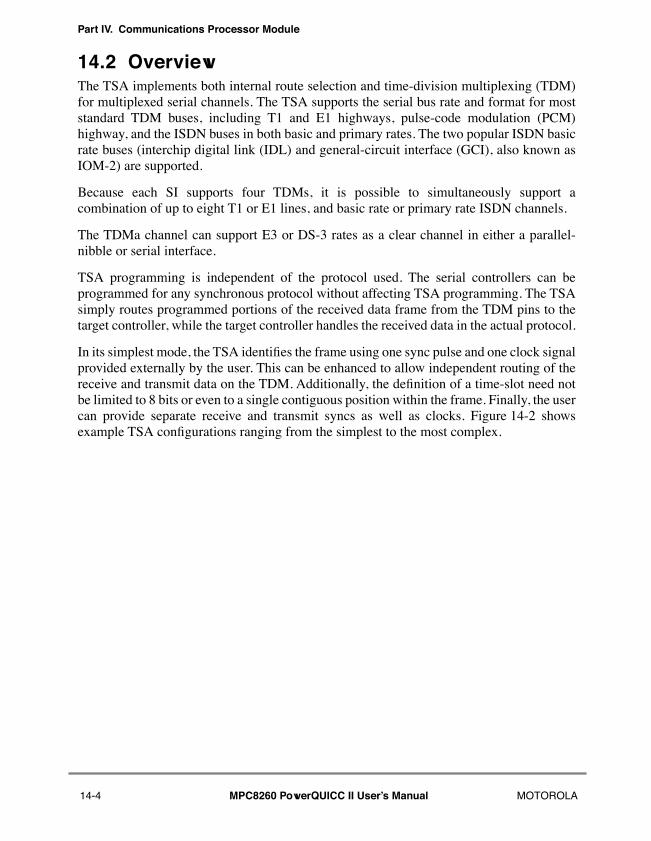
Part IV. Communications Processor Module
14.2 OverviewThe TSA implements both internal route selection and time-division multiplexing (TDM)for multiplexed serial channels. The TSA supports the serial bus rate and format for moststandard TDM buses, including T1 and E1 highways, pulse-code modulation (PCM)highway, and the ISDN buses in both basic and primary rates. The two popular ISDN basicrate buses (interchip digital link (IDL) and general-circuit interface (GCI), also known asIOM-2) are supported.
Because each SI supports four TDMs, it is possible to simultaneously support acombination of up to eight T1 or E1 lines, and basic rate or primary rate ISDN channels.
The TDMa channel can support E3 or DS-3 rates as a clear channel in either a parallel-nibble or serial interface.
TSA programming is independent of the protocol used. The serial controllers can beprogrammed for any synchronous protocol without affecting TSA programming. The TSAsimply routes programmed portions of the received data frame from the TDM pins to thetarget controller, while the target controller handles the received data in the actual protocol.
In its simplest mode, the TSA identiÞes the frame using one sync pulse and one clock signalprovided externally by the user. This can be enhanced to allow independent routing of thereceive and transmit data on the TDM. Additionally, the deÞnition of a time-slot need notbe limited to 8 bits or even to a single contiguous position within the frame. Finally, the usercan provide separate receive and transmit syncs as well as clocks. Figure 14-2 showsexample TSA conÞgurations ranging from the simplest to the most complex.
14-4 MPC8260 PowerQUICC II UserÕs Manual MOTOROLA
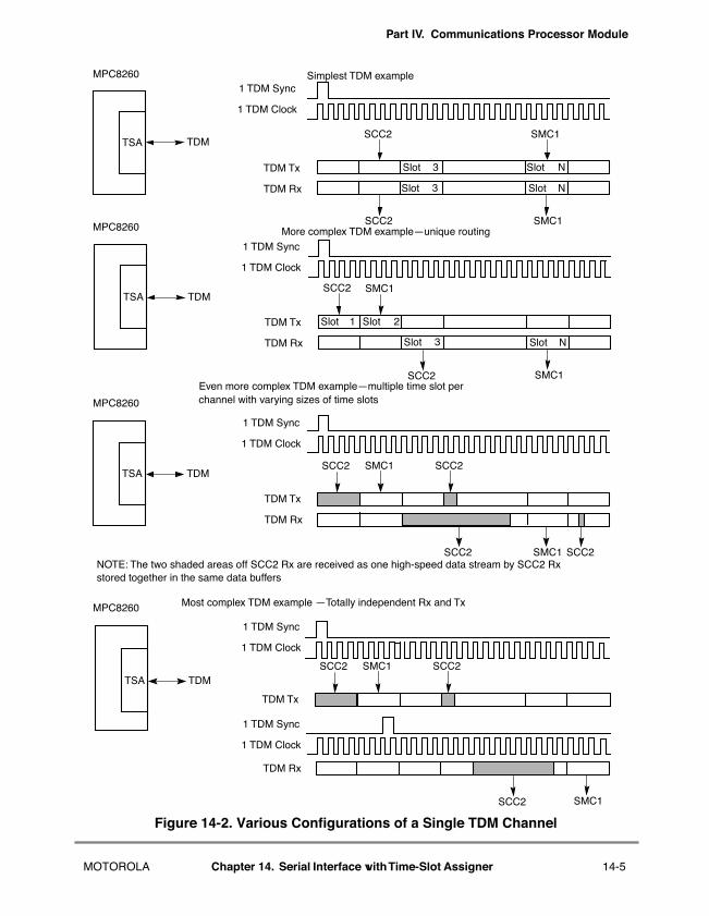
Part IV. Communications Processor Module
Figure 14-2. Various Configurations of a Single TDM Channel
TSA
MPC8260
TDM
TSA
TSA
TSA
Slot
Slot
3
3 Slot
Slot
N
N
TDM
TDM
TDM
SCC2 SMC1
SCC2 SMC1
TDM Tx
TDM Rx
Simplest TDM example
Slot 2
Slot N
1 TDM Sync
1 TDM Clock
SMC1
SCC2 SMC1
TDM Tx
TDM Rx
Slot 1
Slot 3
SCC2
More complex TDM exampleÑunique routing
SCC2 SMC1 SCC2
SCC2 SMC1 SCC2
TDM Tx
TDM Rx
Even more complex TDM exampleÑmultiple time slot per
SCC2 SMC1 SCC2
TDM Tx
SCC2
TDM Rx
SMC1
Most complex TDM example ÑTotally independent Rx and Tx
NOTE: The two shaded areas off SCC2 Rx are received as one high-speed data stream by SCC2 Rxstored together in the same data buffers
channel with varying sizes of time slots
MPC8260
MPC8260
MPC8260
1 TDM Sync
1 TDM Clock
1 TDM Sync
1 TDM Clock
1 TDM Sync
1 TDM Clock
1 TDM Sync
1 TDM Clock
MOTOROLA Chapter 14. Serial Interface with Time-Slot Assigner 14-5
Part IV. Communications Processor Module
At its most ßexible, the TSA can provide four separate TDM channels, each withindependent receive and transmit routing assignments and independent sync pulse andclock inputs. Thus, the TSA can support eight, independent, half-duplex TDM sources, fourin reception and four in transmission, using eight sync inputs and eight clock inputs.Figure 14-3 shows a dual-channel example.
Figure 14-3. Dual TDM Channel Example
In addition to channel programming, the TSA supports up to four strobe outputs that maybe asserted on a bit or byte basis. These strobes are completely independent from thechannel routing used by the SCCs and SMCs. The strobe outputs are useful for interfacingto other devices that do not support the multiplexed interface or for enabling/disablingthree-state I/O buffers in a multiple-transmitter architecture. Notice that open-drainprogramming on the TXDx pins that supports a multiple-transmitter architecture occurs inthe parallel I/O block. These strobes can also be used for generating output wave forms tosupport such applications as stepper-motor control.
Most TSA programming is done in the two 256- ´ 16-bit SIx RAMs. These SIx RAMs aredirectly accessible by the core in the internal register section of the MPC8260 and are not
SCC3 SMC1
TDMa Rx
TSATDMa
TDMb
TDMa Tx SYNC
TDMa Tx CLOCK
SCC2 SMC1 SCC2
TDMa Rx Sync
TDMa Rx Clock
TDMa Rx
SCC3 SCC4
TDMa Tx
TDMb Tx Sync
TDMb Tx Clock
TDMb Rx Sync
TDMb Rx Clock
SCC2 SMC1
TDMb Rx
Note: SCCs can receive on one TDM and transmit on another (SCC2 and SCC3).
14-6 MPC8260 PowerQUICC II UserÕs Manual MOTOROLA
Part IV. Communications Processor Module
associated with the dual-port RAM. One SIx RAM is always used to program the transmitrouting; the other is always used to program the receive routing. SIx RAMs can be used todeÞne the number of bits/bytes to be routed to the MCC, FCC, SCC, or SMC and determinewhen external strobes are to be asserted and negated.
The size of the SIx RAM available for time-slot programming depends on the userÕsconÞguration. The user deÞnes how many of the 256 entries are related to each TDM. Theresolution of the division is by fractions of 32. If on-the-ßy changes are allowed, the SIxRAM entries are reduced according to the userÕs programming. The maximum frame lengththat can be supported in any conÞguration is 16,384 bits.
The maximum external serial clock that may be an input to the TSA is CPM CLK/3.
The SI supports two testing modesÑecho and loopback.
¥ The echo mode provides a return signal from the physical interface by retransmitting the signal it has received. The physical interface echo mode differs from the individual FCC or SCC echo mode in that it can operate on the entire TDM signal rather than just on a particular serial channel.
¥ Loopback mode causes the physical interface to receive the same signal it is sending. The SI loopback mode checks more than the individual serial loopback; it checks both the SI and the internal channel routes.
Note that the ßexibility described in the preceding section can be applied to each of the fourTDM channels and to all serial interfaces independently.
14.3 Enabling Connections to TSAEach serial interface can be independently enabled to connect to one of the following: TSA,UTOPIA, MII, or dedicated external pins. Note the following:
¥ Each FCC can be connected to a dedicated MII or one of four TDMs. FCC1 can also be connected to a 8-/16-bit UTOPIA level-2 interface; FCC2 can also be connected to an 8-bit UTOPIA level-2 interface.
¥ Each SCC or SMC can be connected to one of four TDMs or to its own set of pins.
¥ The MCC can be connected to one of the four TDMs with different numbers of channels.
The four TDMs are connected to four independent TDM interfaces. Figure 14-4 illustratesthe connection between the TSA and the serial interfaces. The connection is made byprogramming the CPM mux. See Chapter 15, ÒCPM Multiplexing.Ó Once the connectionsare made, the exact routing decisions are made in the SIx RAM.
MOTOROLA Chapter 14. Serial Interface with Time-Slot Assigner 14-7
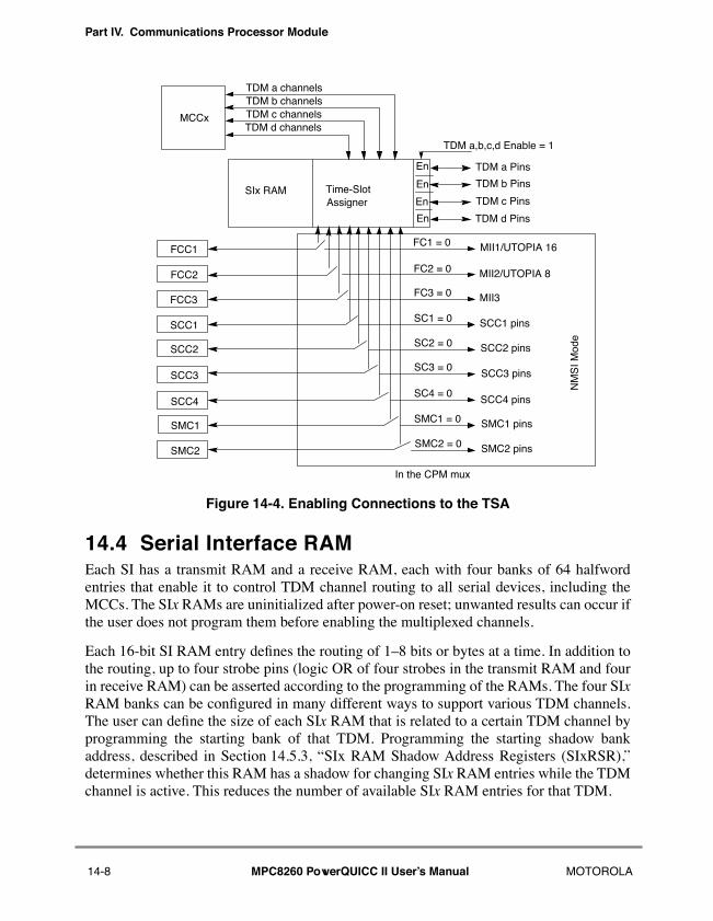
Part IV. Communications Processor Module
Figure 14-4. Enabling Connections to the TSA
14.4 Serial Interface RAMEach SI has a transmit RAM and a receive RAM, each with four banks of 64 halfwordentries that enable it to control TDM channel routing to all serial devices, including theMCCs. The SIx RAMs are uninitialized after power-on reset; unwanted results can occur ifthe user does not program them before enabling the multiplexed channels.
Each 16-bit SI RAM entry deÞnes the routing of 1Ð8 bits or bytes at a time. In addition tothe routing, up to four strobe pins (logic OR of four strobes in the transmit RAM and fourin receive RAM) can be asserted according to the programming of the RAMs. The four SIxRAM banks can be conÞgured in many different ways to support various TDM channels.The user can deÞne the size of each SIx RAM that is related to a certain TDM channel byprogramming the starting bank of that TDM. Programming the starting shadow bankaddress, described in Section 14.5.3, ÒSIx RAM Shadow Address Registers (SIxRSR),Ódetermines whether this RAM has a shadow for changing SIx RAM entries while the TDMchannel is active. This reduces the number of available SIx RAM entries for that TDM.
En
En
En
En
SIx RAM Time-SlotAssigner
TDM a,b,c,d Enable = 1
TDM a Pins
TDM b Pins
TDM c Pins
TDM d Pins
FCC1
FCC2
FCC3
SCC1
SCC2
SCC3
SCC4
SMC1
SMC2
MII1/UTOPIA 16FC1 = 0
MII2/UTOPIA 8FC2 = 0
MII3FC3 = 0
SCC1 pinsSC1 = 0
SCC2 pinsSC2 = 0
SCC3 pinsSC3 = 0
SCC4 pinsSC4 = 0
SMC1 pinsSMC1 = 0
SMC2 pinsSMC2 = 0
MCCx
TDM a channelsTDM b channelsTDM c channelsTDM d channels
NM
SI M
ode
In the CPM mux
14-8 MPC8260 PowerQUICC II UserÕs Manual MOTOROLA
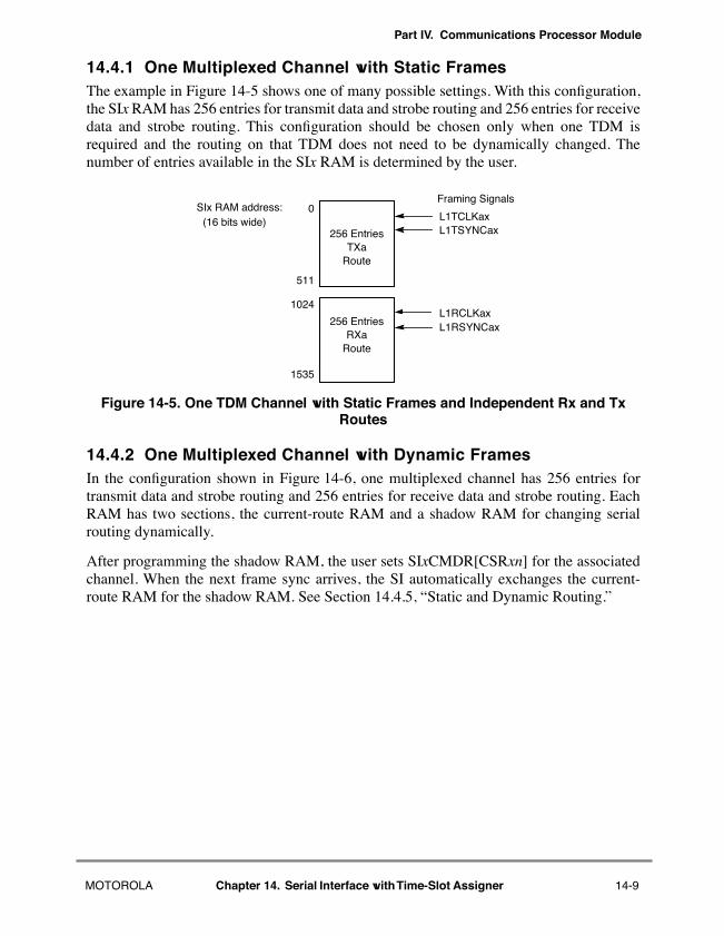
Part IV. Communications Processor Module
14.4.1 One Multiplexed Channel with Static FramesThe example in Figure 14-5 shows one of many possible settings. With this conÞguration,the SIx RAM has 256 entries for transmit data and strobe routing and 256 entries for receivedata and strobe routing. This conÞguration should be chosen only when one TDM isrequired and the routing on that TDM does not need to be dynamically changed. Thenumber of entries available in the SIx RAM is determined by the user.
Figure 14-5. One TDM Channel with Static Frames and Independent Rx and Tx Routes
14.4.2 One Multiplexed Channel with Dynamic FramesIn the conÞguration shown in Figure 14-6, one multiplexed channel has 256 entries fortransmit data and strobe routing and 256 entries for receive data and strobe routing. EachRAM has two sections, the current-route RAM and a shadow RAM for changing serialrouting dynamically.
After programming the shadow RAM, the user sets SIxCMDR[CSRxn] for the associatedchannel. When the next frame sync arrives, the SI automatically exchanges the current-route RAM for the shadow RAM. See Section 14.4.5, ÒStatic and Dynamic Routing.Ó
256 EntriesTXa
Route
Framing Signals
L1TCLKaxL1TSYNCax
SIx RAM address:
256 EntriesRXa
Route
511
1535
1024L1RCLKaxL1RSYNCax
(16 bits wide)0
MOTOROLA Chapter 14. Serial Interface with Time-Slot Assigner 14-9
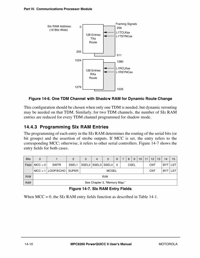
Part IV. Communications Processor Module
Figure 14-6. One TDM Channel with Shadow RAM for Dynamic Route Change
This conÞguration should be chosen when only one TDM is needed, but dynamic reroutingmay be needed on that TDM. Similarly, for two TDM channels, the number of SI
x
RAMentries are reduced for every TDM channel programmed for shadow mode.
14.4.3 Programming SI
x
RAM Entries
The programming of each entry in the SI
x
RAM determines the routing of the serial bits (orbit groups) and the assertion of strobe outputs. If MCC is set, the entry refers to thecorresponding MCC; otherwise, it refers to other serial controllers. Figure 14-7 shows theentry Þelds for both cases.
When MCC = 0, the SI
x
RAM entry Þelds function as described in Table 14-1.
Bits 0 1 2 3 4 5 6 7 8 9 10 11 12 13 14 15
Field MCC = 0 SWTR SSEL1 SSEL2 SSEL3 SSEL4 0 CSEL CNT BYT LST
MCC = 1 LOOP/ECHO SUPER MCSEL CNT BYT LST
R/W R/W
Addr See Chapter 3, ÒMemory Map.Ó
Figure 14-7. SI
x
RAM Entry Fields
128 EntriesTXa
Route
Framing Signals
L1TCLKa
x
L1TSYNCa
x
SI
x
RAM Address:
128 EntriesRXa
Route
255
1279
1024
L1RCLKa
x
L1RSYNCa
x
1280
256
511
1535
(16 Bits Wide)0
14-10 MPC8260 PowerQUICC II UserÕs Manual MOTOROLA
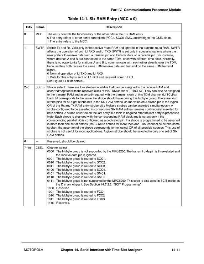
Part IV. Communications Processor Module
Table 14-1. SI
x
RAM Entry (MCC = 0)
Bits Name Description
0 MCC The entry controls the functionality of the other bits in the SI
x
RAM entry.
0 The entry refers to other serial controllers (FCCs, SCCs, SMC, according to the CSEL Þeld).1 The entry refers to the MCC.
1 SWTR Switch Tx and Rx. Valid only in the receive route RAM and ignored in the transmit route RAM. SWTR affects the operation of both L1RXD and L1TXD. SWTR is set only in special situations where the user prefers to receive data from a transmit pin and transmit data on a receive pin. For instance, where devices A and B are connected to the same TDM, each with different time-slots. Normally, there is no opportunity for stations A and B to communicate with each other directly over the TDM, because they both receive the same TDM receive data and transmit on the same TDM transmit signal. 0 Normal operation of L1TXD and L1RXD.1 Data for this entry is sent on L1RXD and received from L1TXD.See Figure 14-8 for details.
2Ð5 SSELx Strobe select. There are four strobes available that can be assigned to the receive RAM and asserted/negated with the received clock of this TDM channel (L1RCLKx). They can also be assigned to the transmit RAM and asserted/negated with the transmit clock of this TDM channel (L1TCLKx). Each bit corresponds to the value the strobe should have during this bit/byte group. There are four strobe pins for all eight strobe bits in the SI
x
RAM entries, so the value on a strobe pin is the logical OR of the Rx and Tx RAM entry strobe bit.s Multiple strobes can be asserted simultaneously. A strobe conÞgured to be asserted in consecutive SI
x
RAM entries remains continuously asserted for both entries. A strobe asserted on the last entry in a table is negated after the last entry is processed. Note: Each strobe is changed with the corresponding RAM clock and is output only if the corresponding parallel I/O is conÞgured as a dedicated pin. If a strobe is programmed to be asserted in more than one set of entries (the SI route entries for more then one TDM channel select the same strobe), the assertion of the strobe corresponds to the logical OR of all possible sources. This use of strobes is not useful for most applications. A given strobe should be selected in only one set of SI
x
RAM entries.
6 Ñ Reserved, should be cleared.
7Ð10 CSEL Channel select0000 The bit/byte group is not supported by the MPC8260. The transmit data pin is three-stated and
the receive data pin is ignored.0001 The bit/byte group is routed to SCC1.0010 The bit/byte group is routed to SCC2.0011 The bit/byte group is routed to SCC3.0100 The bit/byte group is routed to SCC4.0101 The bit/byte group is routed to SMC1.0110 The bit/byte group is routed to SMC2.0111 The bit/byte group is not supported by the MPC8260. This code is also used in SCIT mode as
the D channel grant. See Section 14.7.2.2, ÒSCIT Programming.Ó1000 Reserved.1001 The bit/byte group is routed to FCC1.1010 The bit/byte group is routed to FCC2.1011 The bit/byte group is routed to FCC3.11xx Reserved.
MOTOROLA Chapter 14. Serial Interface with Time-Slot Assigner 14-11
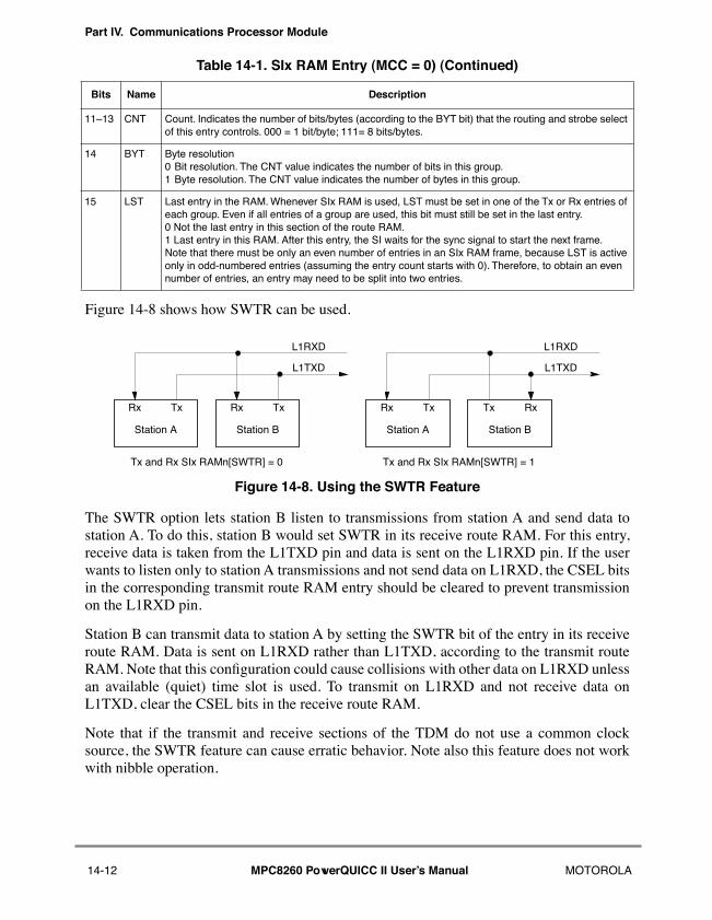
Part IV. Communications Processor Module
Figure 14-8 shows how SWTR can be used.
Figure 14-8. Using the SWTR Feature
The SWTR option lets station B listen to transmissions from station A and send data tostation A. To do this, station B would set SWTR in its receive route RAM. For this entry,receive data is taken from the L1TXD pin and data is sent on the L1RXD pin. If the userwants to listen only to station A transmissions and not send data on L1RXD, the CSEL bitsin the corresponding transmit route RAM entry should be cleared to prevent transmissionon the L1RXD pin.
Station B can transmit data to station A by setting the SWTR bit of the entry in its receiveroute RAM. Data is sent on L1RXD rather than L1TXD, according to the transmit routeRAM. Note that this conÞguration could cause collisions with other data on L1RXD unlessan available (quiet) time slot is used. To transmit on L1RXD and not receive data onL1TXD, clear the CSEL bits in the receive route RAM.
Note that if the transmit and receive sections of the TDM do not use a common clocksource, the SWTR feature can cause erratic behavior. Note also this feature does not workwith nibble operation.
11Ð13 CNT Count. Indicates the number of bits/bytes (according to the BYT bit) that the routing and strobe select
of this entry controls. 000 = 1 bit/byte; 111= 8 bits/bytes.
14 BYT Byte resolution0 Bit resolution. The CNT value indicates the number of bits in this group.1 Byte resolution. The CNT value indicates the number of bytes in this group.
15 LST Last entry in the RAM. Whenever SI
x
RAM is used, LST must be set in one of the Tx or Rx entries of each group. Even if all entries of a group are used, this bit must still be set in the last entry.0 Not the last entry in this section of the route RAM.1 Last entry in this RAM. After this entry, the SI waits for the sync signal to start the next frame.Note that there must be only an even number of entries in an SI
x
RAM frame, because LST is active only in odd-numbered entries (assuming the entry count starts with 0). Therefore, to obtain an even number of entries, an entry may need to be split into two entries.
Table 14-1. SI
x
RAM Entry (MCC = 0) (Continued)
Bits Name Description
Rx
Station A
Tx Rx
Station B
Tx
L1TXD
L1RXD
Rx
Station A
Tx Tx
Station B
Rx
L1TXD
L1RXD
Tx and Rx SIx RAMn[SWTR] = 1Tx and Rx SIx RAMn[SWTR] = 0
14-12 MPC8260 PowerQUICC II UserÕs Manual MOTOROLA
Part IV. Communications Processor Module
When MCC = 1, the SI
x
RAM entry Þelds function as described in Table 14-2.
14.4.4 SI
x
RAM Programming Example
This example shows how to program the RAM to support the 10-bit IDL bus. Figure 14-23shows the 10-bit IDL bus format. In this example, the TSA supports the B1 channel withSCC2, the D channel with SCC1, the Þrst 4 bits of the B2 channel with an external device(using a strobe to enable the external device), and the last 4 bits of B2 with SMC1.Additionally, the TSA marks the D channel with another strobe signal.
Table 14-2. SI
x
RAM Entry (MCC = 1)
Bits Name Description
0 MCC If MCC =1, the other SI
x
RAM entries in this table are valid:
1 LOOP/ECHO
Channel loopback or echo. 0 Normal mode of operation.1 Operation depends on the following conÞgurations:
In the receive SI
x
RAM, this bit selects loopback mode for this MCC channel. The channelÕs transmit data is sent to both the receiverÕs input and to the data output line.In the transmit SI
x
RAM, this bit selects echo mode for this MCC channel. The channelÕs receive data is sent both to the transmitterÕs line and to the receiverÕs input.
To use the loop/echo modes, program the receive and transmit SI
x
RAMs identically, except that the LOOP/ECHO bit should be set in only one of the entry pairs; that is, select only one of the modes (echo or loopback, not both) per MCC slot. Also, the receive and transmit clocks must be identical.
2 SUPER MCC super channel enable. See Section 27.5, ÒSuper-Channel Table.Ó0 The current entry refers to a regular channel.1 The current entry refers to a super channel.
3Ð10 MCSEL MCC channel select. Indicates the MCC channel the bit/byte group is routed to. 0000_0000 selects channel 0; 1111_1111, selects channel 255.For SI1 use values 0Ð127 and for SI2 use values 128Ð255. Note that the channel programming must be coherent with the MCCF; see Section 27.8, ÒMCC ConÞguration Registers (MCCFx).Ó
11Ð13 CNT Count. If SUPER = 0 (normal mode), CNT indicates the number of bits/bytes (according to the BYT bit) that the routing select of this entry controls. 000 = 1 bit/byte; 111 = 8 bits/bytes.If SUPER = 1 (MCC super channel), CNT and BYT together indicate whether the current entry is the Þrst byte of the MCC super channel.CNT= 000 and BYT = 1ÑThe current entry is the Þrst byte of this MCC super channel.CNT= 111 and BYT = 0ÑThe current entry is not the Þrst byte of this MCC super channel.Note that because all SI
x
RAM entries relating to super channels must be 1-byte in resolution, only the above two combinations of CNT and BYT are allowed when SUPER = 1.
14 BYT Byte resolution0 Bit resolution. The CNT value indicates the number of bits in this group.1 Byte resolution. The CNT value indicates the number of bytes in this group.
15 LST Last entry in the RAM. Whenever the SI
x
RAM is used, LST must be set in one of the Tx or Rx entries of each group. Even if all entries of a group are used, LST must still be set in the last entry.0 Not the last entry in this section of the route RAM.1 Last entry in this RAM. After this entry, the SI waits for the sync signal to start the next frame.Note that there must be only an even number of entries in an SI
x
RAM frame, because LST is active only in odd-numbered entries (assuming the entry count starts with 0). Therefore, to obtain an even number of entries, an entry may need to be split into two entries.
MOTOROLA Chapter 14. Serial Interface with Time-Slot Assigner 14-13
Part IV. Communications Processor Module
First, divide the frame from the start (the sync) to the end of the frame according to thesupport that is required:
¥ 8 bits (B1)ÑSCC2
¥ 1 bit (D)ÑSCC1 + strobe 1
¥ 1 bitÑno support
¥ 4 bits (B2)Ñstrobe 2
¥ 4 bits (B2)ÑSMC1
¥ 1 bit (D)ÑSCC1 + strobe 1
Each of these six divisions can be supported by a single SI
x
RAM entry. Thus, six SI
x
RAMentries are needed. See Table 14-3.
Note that because IDL requires the same routing for both receive and transmit, an exactduplicate of the above entries should be written to both the receive and transmit sections ofthe SI
x
RAM. Then SI
x
MR[CRTx] can be used to instruct the SI
x
RAM to use the sameclock and sync to simultaneously control both sets of SI
x
RAM entries.
14.4.5 Static and Dynamic Routing
The SI
x
RAM has two operating modes for the TDMs:
¥ Static routing. The number of SI
x
RAM entries is determined by the banks the user relates to the corresponding TDM and is divided into two parts (Rx and Tx). Three requirements must be met before the new routing takes effect.
Ñ All serial devices connected to the TSA must be disabled.
Ñ SI routing can be modiÞed.
Ñ All appropriate serial devices connected to the TSA must be reenabled.
Table 14-3. SI
x
RAM Entry Descriptions
Entry Number
SI
x
RAM Entry
MCC SWTR SSEL CSEL CNT BYT LST Description
0 0 0 0000 0010 000 1 0 8-bit SCC2
1 0 0 1000 0001 000 0 0 1-bit SCC1 strobe1
2 0 0 0000 0000 000 0 0 1-bit no support
3 0 0 0100 0000 011 0 0 4-bit strobe2
4 0 0 0000 0101 011 0 0 4-bit SMC1
5 0 0 1000 0001 000 0 1 1-bit SCC1 strobe1
14-14 MPC8260 PowerQUICC II UserÕs Manual MOTOROLA
Part IV. Communications Processor Module
¥ Dynamic routing. A TDMÕs routing deÞnition can be modiÞed while FCCs, MCCs, SCCs, or SMCs are connected to the TDM. The number of SI
x
RAM entries is determined by the banks the user relates to the corresponding TDM channel and is divided into four parts (Rx, Rx shadow, Tx, and Tx shadow).
Dynamic changes divide portions of the SI
x
RAM into current-route and shadow RAM.Once the current-route RAM is programmed, the TSA and SI channels are enabled, andTSA operation begins. When a change in routing is required, the shadow RAM must beprogrammed with the new route and SI
x
CMDR[CSR
xn
] must be set. As a result, as soonas the corresponding sync arrives the SI exchanges the shadow RAM with the current-routeRAM and resets CSR
xn
to indicate that the operation is complete. At this time, the user maychange the routing again. Notice that the original current-route RAM is now the shadowRAM and vice versa. Figure 14-9 shows an example of the shadow RAM exchange processfor two TDM channels both with half of the RAM as a shadow.
If for instance one TDM with dynamic changes is programmed to own all four banks, andthe shadow is programmed to the last two banks, the initial current-route RAM addressesin the SI
x
RAM are as follows.
¥ 0Ð255: TXa route
¥ 1024Ð1279: RXa route
The initial shadow RAMs are at addresses:
¥ 256Ð511: TXa route
¥ 1280Ð1535: RXa route
The user can read any RAM at any time, but for proper SI operation the user must notattempt to write the current-route RAM. The SI
x
status register (SI
x
STR) can be read to Þndout which part of the RAM is the current-route RAM. The user can also externally connectone of the strobes to an interrupt pin to generate an interrupt on a particular SI
x
RAM entrystarting or ending execution by the TSA.
An example is shown in Figure 14-9.
MOTOROLA Chapter 14. Serial Interface with Time-Slot Assigner 14-15
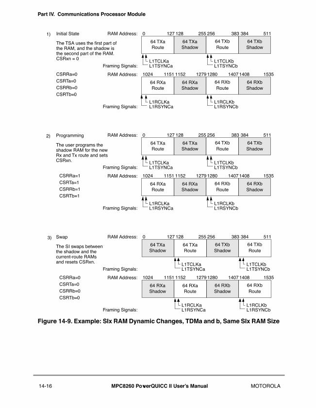
Part IV. Communications Processor Module
Figure 14-9. Example: SIx RAM Dynamic Changes, TDMa and b, Same SIx RAM Size
L1TCLKbL1TSYNCb
64 TXbShadow
64 TXa 64 TXbRouteRoute
The TSA uses the first part of
Framing Signals:L1TCLKaL1TSYNCa
1) Initial State
the RAM, and the shadow is64 TXaShadow
0 127 128 255 256 383 384 511
CSRRa=0
The user programs the
2) Programming
shadow RAM for the new
The SI swaps between
Swap
the shadow and the
Rx and Tx route and sets
the second part of the RAM. CSRxn = 0
current-route RAMs
1024 1151 1152 1279 1280 1407 1408 1535
RAM Address:
CSRTa=0CSRRb=0CSRTb=0
CSRRa=1CSRTa=1CSRRb=1CSRTb=1
CSRRa=0CSRTa=0CSRRb=0CSRTb=0
L1RCLKbL1RSYNCb
64 RXbShadow
64 RXa 64 RXbRouteRoute
Framing Signals:L1RCLKaL1RSYNCa
64 RXaShadow
RAM Address:
CSRxn. L1TCLKbL1TSYNCb
64 TXbShadow
64 TXa 64 TXbRouteRoute
Framing Signals:L1TCLKaL1TSYNCa
64 TXaShadow
0 127 128 255 256 383 384 511
1024 1151 1152 1279 1280 1407 1408 1535
RAM Address:
L1RCLKbL1RSYNCb
64 RXbShadow
64 RXa 64 RXbRouteRoute
Framing Signals:L1RCLKaL1RSYNCa
64 RXaShadow
RAM Address:
and resets CSRxn. L1TCLKbL1TSYNCb
64 TXbShadow
64 TXa 64 TXbRouteRoute
Framing Signals:L1TCLKaL1TSYNCa
64 TXaShadow
0 127 128 255 256 383 384 511
1024 1151 1152 1279 1280 1407 1408 1535
RAM Address:
L1RCLKbL1RSYNCb
64 RXbShadow
64 RXa 64 RXbRouteRoute
Framing Signals:L1RCLKaL1RSYNCa
64 RXaShadow
RAM Address:
3)
14-16 MPC8260 PowerQUICC II UserÕs Manual MOTOROLA
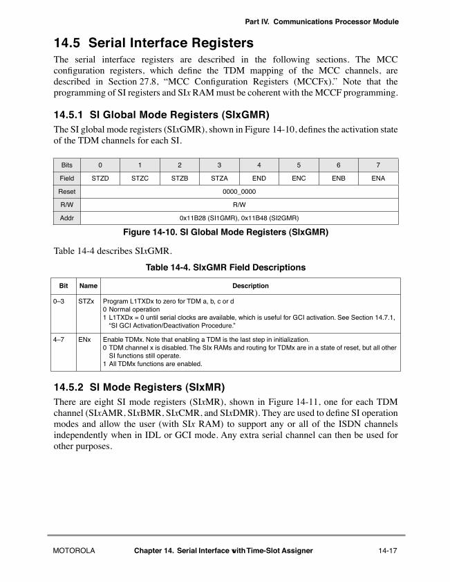
Part IV. Communications Processor Module
14.5 Serial Interface RegistersThe serial interface registers are described in the following sections. The MCCconÞguration registers, which deÞne the TDM mapping of the MCC channels, aredescribed in Section 27.8, ÒMCC ConÞguration Registers (MCCFx).Ó Note that theprogramming of SI registers and SIx RAM must be coherent with the MCCF programming.
14.5.1 SI Global Mode Registers (SIxGMR)The SI global mode registers (SIxGMR), shown in Figure 14-10, deÞnes the activation stateof the TDM channels for each SI.
Table 14-4 describes SIxGMR.
14.5.2 SI Mode Registers (SIxMR)There are eight SI mode registers (SIxMR), shown in Figure 14-11, one for each TDMchannel (SIxAMR, SIxBMR, SIxCMR, and SIxDMR). They are used to deÞne SI operationmodes and allow the user (with SIx RAM) to support any or all of the ISDN channelsindependently when in IDL or GCI mode. Any extra serial channel can then be used forother purposes.
Bits 0 1 2 3 4 5 6 7
Field STZD STZC STZB STZA END ENC ENB ENA
Reset 0000_0000
R/W R/W
Addr 0x11B28 (SI1GMR), 0x11B48 (SI2GMR)
Figure 14-10. SI Global Mode Registers (SIxGMR)
Table 14-4. SIxGMR Field Descriptions
Bit Name Description
0Ð3 STZx Program L1TXDx to zero for TDM a, b, c or d0 Normal operation1 L1TXDx = 0 until serial clocks are available, which is useful for GCI activation. See Section 14.7.1,
ÒSI GCI Activation/Deactivation Procedure.Ó
4Ð7 ENx Enable TDMx. Note that enabling a TDM is the last step in initialization.0 TDM channel x is disabled. The SIx RAMs and routing for TDMx are in a state of reset, but all other
SI functions still operate.1 All TDMx functions are enabled.
MOTOROLA Chapter 14. Serial Interface with Time-Slot Assigner 14-17
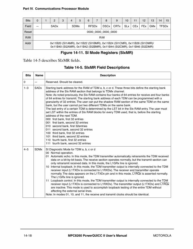
Part IV. Communications Processor Module
Table 14-5 describes SIxMR Þelds.
Bits 0 1 2 3 4 5 6 7 8 9 10 11 12 13 14 15
Field Ñ SADx SDMx RFSDx DSCx CRTx SLx CEx FEx GMx TFSDx
Reset 0000_0000_0000_0000
R/W R/W
Addr 0x11B20 (SI1AMR), 0x11B22 (SI1BMR), 0x11B24 (SI1CMR), 0x11B26 (SI1DMR)/0x11B40 (SI2AMR), 0x11B42 (SI2BMR), 0x11B44 (SI2CMR), 0x11B46 (SI2DMR)
Figure 14-11. SI Mode Registers (SIxMR)
Table 14-5. SIxMR Field Descriptions
Bits Name Description
0 Ñ Reserved. Should be cleared.
1Ð3 SADx Starting bank address for the RAM of TDM a, b, c or d. These three bits deÞne the starting bank address of the SIx RAM section that belongs to TDMx channel. Note: As noted previously, the SIx RAM contains four banks of 64 entries for receive and four banks of 64 entries for transmit. The starting bank address of each TDM can be programmed with a granularity of 32 entries. The user can put the shadow RAM section of the same TDM on the same bank, but the user cannot put two different TDMs on the same bank.The last entry of a certain TDM is determined by the LST bit in the SIx RAM entry. The user must set LST within the entries of SIx RAM blocks for every TDM used, that is, before the starting address of the next TDM.000 Þrst bank, Þrst 32 entries001 Þrst bank, second 32 entries010 second bank, Þrst 32entries011 second bank, second 32 entries100 third bank, Þrst 32 entries101 third bank, second 32 entries110 fourth bank, Þrst 32 entries111 fourth bank, second 32 entries
4Ð5 SDMx SI Diagnostic Mode for TDM a, b, c or d00 Normal operation.01 Automatic echo. In this mode, the TDM transmitter automatically retransmits the TDM received
data on a bit-by-bit basis. The receive section operates normally, but the transmit section can only retransmit received data. In this mode, the L1GRx line is ignored.
10 Internal loopback. In this mode, the TDM transmitter output is internally connected to the TDM receiver input (L1TXDx is connected to L1RXDx). The receiver and transmitter operate normally. The data appears on the L1TXDx pin and in this mode, L1RQx is asserted normally. The L1GRx line is ignored.
11 Loopback control. In this mode, the TDM transmitter output is internally connected to the TDM receiver input (L1TXDx is connected to L1RXDx). The transmitter output (L1TXDx) and L1RQx are inactive. This mode is used to accomplish loopback testing of the entire TDM without affecting the external serial lines.
Note: In modes 01, 10, and 11, the receive and transmit clocks should be identical.
14-18 MPC8260 PowerQUICC II UserÕs Manual MOTOROLA
Part IV. Communications Processor Module
6Ð7 RFSDx Receive frame sync delay for TDM a, b, c, or d. Determines the number of clock delays between the receive sync and the Þrst bit of the receive frame. Even if CRTx is set, these bits do not control the delay for the transmit frame.00 No bit delay. The Þrst bit of the frame is transmitted/received on the same clock as the sync; use
for GCI.01 1-bit delay. Use for IDL10 2-bit delay11 3-bit delayFigure 14-12 and Figure 14-13 show how these bits are used.
8 DSCx Double speed clock for TDM a, b, c or d. Some TDMs, such as GCI, deÞne the input clock to be twice as fast as the data rate and this bit controls this option.0 The channel clock (L1RCLKx and/or L1TCLKx) is equal to the data clock. Use for IDL and most
TDM formats.1 The channel clock rate is twice the data rate. Use for GCI.
9 CRTx Common receive and transmit pins for TDM a, b, c or d. Useful when the transmit and receive sections of a given TDM use the same clock and sync signals. In this mode, L1TCLKx and L1TSYNCx pins can be used as general-purpose I/O pins. 0 Separate pins. The receive section of this TDM uses L1RCLKx and L1RSYNCx pins for framing
and the transmit section uses L1TCLKx and L1TSYNCx for framing.1 Common pins. The receive and transmit sections of this TDM use L1RCLKx as clock pin of
channel x and L1RSYNCx as the receive and transmit sync pin. Use for IDL and GCI. RFSD and TFSD are independent of one another in this mode.
10 SLx Sync level for TDM a, b, c, or d. 0 The L1RSYNCx and L1TSYNCx signals are active on logic Ò1Ó.1 The L1RSYNCx and L1TSYNCx signals are active on logic Ò0Ó.
11 CEx Clock edge for TDM a, b, c or d. The function depends on DSCx. When DSCx = 0:0 The data is sent on the rising edge of the clock and received on the falling edge (use for IDL).1 The data is sent on the falling edge of the clock and received on the rising edge.When DSCx = 1:0 The data is sent on the rising edge of the clock and received on the rising edge.1 The data is sent on the falling edge of the clock and received on the falling edge (use for GCI).See Figure 14-14 and Figure 14-15.
12 FEx Frame sync edge for TDM a, b, c or d. Determines whether L1RSYNCx and L1TSYNCx pulses are sampled with the falling/rising edge of the channel clock. See Figure 14-13, Figure 14-14, Figure 14-15, and Figure 14-16. 0 Falling edge. Use for IDL and GCI.1 Rising edge.
Table 14-5. SIxMR Field Descriptions (Continued)
Bits Name Description
MOTOROLA Chapter 14. Serial Interface with Time-Slot Assigner 14-19
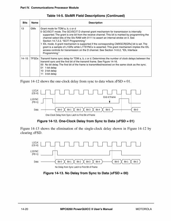
Part IV. Communications Processor Module
Figure 14-12 shows the one-clock delay from sync to data when xFSD = 01.
Figure 14-12. One-Clock Delay from Sync to Data (xFSD = 01)
Figure 14-13 shows the elimination of the single-clock delay shown in Figure 14-12 byclearing xFSD.
Figure 14-13. No Delay from Sync to Data (xFSD = 00)
13 GMx Grant mode for TDM a, b, c or d0 GCI/SCIT mode. The GCI/SCIT D channel grant mechanism for transmission is internally
supported. The grant is one bit from the receive channel. This bit is marked by programming the channel select bits of the SIx RAM with 0111 to assert an internal strobe on it. See Section 14.7.2.2, ÒSCIT Programming.Ó
1 IDL mode. A grant mechanism is supported if the corresponding CMXSCR[GRx] bit is set. The grant is a sample of L1GRx while L1TSYNCx is asserted. This grant mechanism implies the IDL access controls for transmission on the D channel. See Section 14.6.2, ÒIDL Interface Programming.Ó
14Ð15 TFSDx Transmit frame sync delay for TDM a, b, c or d. Determines the number of clock delays between the transmit sync and the Þrst bit of the transmit frame. See Figure 14-16.00 No bit delay. The Þrst bit of the frame is transmitted/received on the same clock as the sync.01 1-bit delay10 2-bit delay11 3-bit delay
Table 14-5. SIxMR Field Descriptions (Continued)
Bits Name Description
L1CLK
Data
(CE=0)
L1SYNC(FE=1)
Bit-0 Bit-1 Bit-2 Bit-3 Bit-4 Bit-0
One-Clock Delay from Sync Latch to First Bit of Frame
Bit-5
End of Frame
L1CLK
Data
(CE=0)
L1SYNC(FE=1)
Bit-0 Bit-1 Bit-2 Bit-3 Bit-4
No Delay from Sync Latch to First Bit of Frame
Bit-2Bit-1Bit-0
14-20 MPC8260 PowerQUICC II UserÕs Manual MOTOROLA
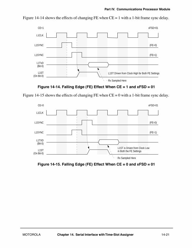
Part IV. Communications Processor Module
Figure 14-14 shows the effects of changing FE when CE = 1 with a 1-bit frame sync delay.
Figure 14-14. Falling Edge (FE) Effect When CE = 1 and xFSD = 01
Figure 14-15 shows the effects of changing FE when CE = 0 with a 1-bit frame sync delay.
Figure 14-15. Falling Edge (FE) Effect When CE = 0 and xFSD = 01
L1TxD
Rx Sampled Here
L1ST
L1SYNC
L1SYNC
L1CLK
(Bit-0)
(On Bit-0)L1ST Driven from Clock High for Both FE Settings
xFSD=01
(FE=0)
(FE=1)
CE=1
L1TXD
Rx Sampled Here
L1ST
L1SYNC
L1SYNC
L1CLK
(Bit-0)
(On Bit-0)
L1ST is Driven from Clock Low
(FE=0)
(FE=1)
CE=0
in Both the FE Settings
xFSD=01
MOTOROLA Chapter 14. Serial Interface with Time-Slot Assigner 14-21
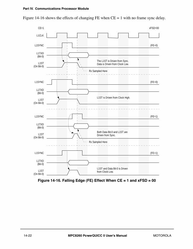
Part IV. Communications Processor Module
Figure 14-16 shows the effects of changing FE when CE = 1 with no frame sync delay.
Figure 14-16. Falling Edge (FE) Effect When CE = 1 and xFSD = 00
L1TXD
L1ST
L1SYNC
L1CLK
(Bit-0)
(On Bit-0)
xFSD=00
(FE=0)
CE=1
The L1ST is Driven from Sync.Data is Driven from Clock Low.
L1TXD
L1ST
L1SYNC
(Bit-0)
(On Bit-0)
(FE=0)
L1ST is Driven from Clock High.
L1TXD
L1ST
L1SYNC
(Bit-0)
(On Bit-0)
(FE=1)
Both Data Bit-0 and L1ST areDriven from Sync.
Rx Sampled Here
Rx Sampled Here
L1TXD
L1ST
L1SYNC
(Bit-0)
(On Bit-0)
(FE=1)
L1ST and Data Bit-0 is Drivenfrom Clock Low.
14-22 MPC8260 PowerQUICC II UserÕs Manual MOTOROLA
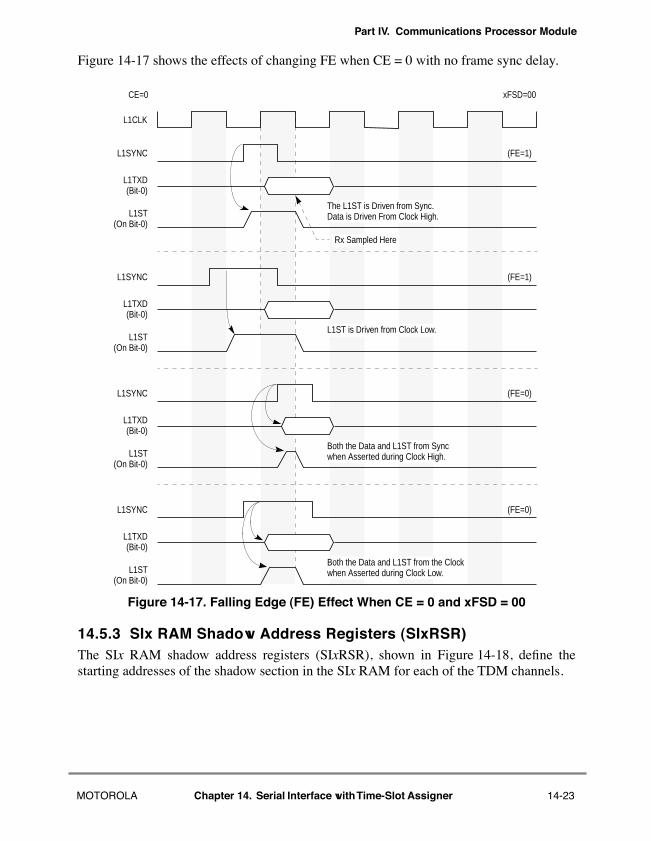
Part IV. Communications Processor Module
Figure 14-17 shows the effects of changing FE when CE = 0 with no frame sync delay.
Figure 14-17. Falling Edge (FE) Effect When CE = 0 and xFSD = 00
14.5.3 SIx RAM Shadow Address Registers (SIxRSR)The SIx RAM shadow address registers (SIxRSR), shown in Figure 14-18, deÞne thestarting addresses of the shadow section in the SIx RAM for each of the TDM channels.
L1TXD
L1ST
L1SYNC
L1CLK
(Bit-0)
(On Bit-0)
xFSD=00
(FE=1)
CE=0
The L1ST is Driven from Sync.Data is Driven From Clock High.
L1TXD
L1ST
L1SYNC
(Bit-0)
(On Bit-0)
(FE=1)
L1ST is Driven from Clock Low.
L1TXD
L1ST
L1SYNC
(Bit-0)
(On Bit-0)
(FE=0)
Both the Data and L1ST from Syncwhen Asserted during Clock High.
Rx Sampled Here
L1TXD
L1ST
L1SYNC
(Bit-0)
(On Bit-0)
(FE=0)
Both the Data and L1ST from the Clockwhen Asserted during Clock Low.
MOTOROLA Chapter 14. Serial Interface with Time-Slot Assigner 14-23
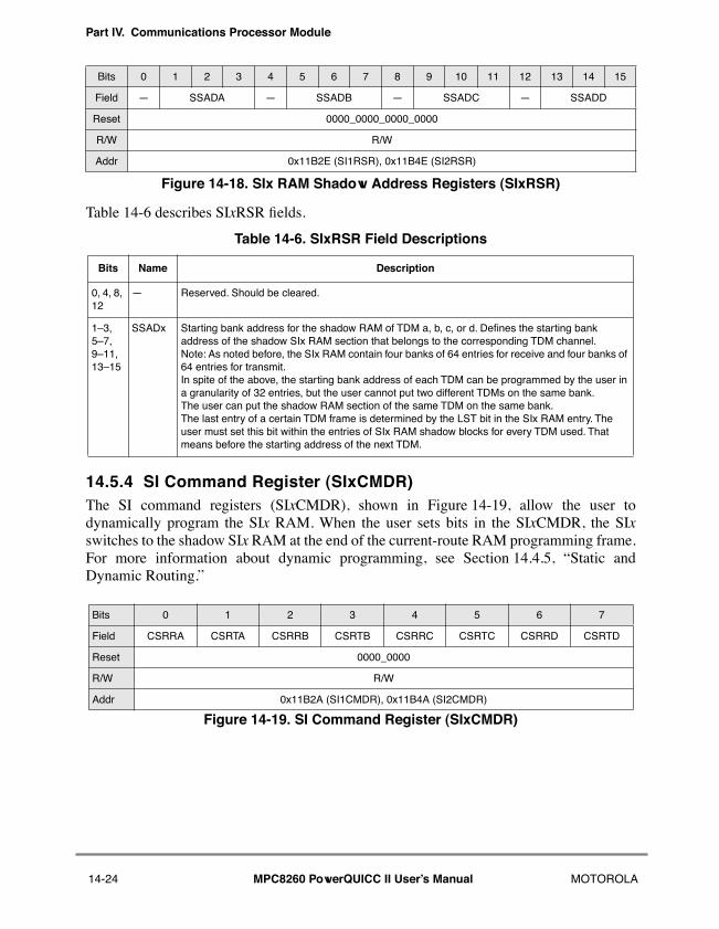
Part IV. Communications Processor Module
Table 14-6 describes SIxRSR Þelds.
14.5.4 SI Command Register (SIxCMDR)The SI command registers (SIxCMDR), shown in Figure 14-19, allow the user todynamically program the SIx RAM. When the user sets bits in the SIxCMDR, the SIxswitches to the shadow SIx RAM at the end of the current-route RAM programming frame.For more information about dynamic programming, see Section 14.4.5, ÒStatic andDynamic Routing.Ó
Bits 0 1 2 3 4 5 6 7 8 9 10 11 12 13 14 15
Field Ñ SSADA Ñ SSADB Ñ SSADC Ñ SSADD
Reset 0000_0000_0000_0000
R/W R/W
Addr 0x11B2E (SI1RSR), 0x11B4E (SI2RSR)
Figure 14-18. SIx RAM Shadow Address Registers (SIxRSR)
Table 14-6. SIxRSR Field Descriptions
Bits Name Description
0, 4, 8, 12
Ñ Reserved. Should be cleared.
1Ð3, 5Ð7, 9Ð11, 13Ð15
SSADx Starting bank address for the shadow RAM of TDM a, b, c, or d. DeÞnes the starting bank address of the shadow SIx RAM section that belongs to the corresponding TDM channel.Note: As noted before, the SIx RAM contain four banks of 64 entries for receive and four banks of 64 entries for transmit.In spite of the above, the starting bank address of each TDM can be programmed by the user in a granularity of 32 entries, but the user cannot put two different TDMs on the same bank.The user can put the shadow RAM section of the same TDM on the same bank.The last entry of a certain TDM frame is determined by the LST bit in the SIx RAM entry. The user must set this bit within the entries of SIx RAM shadow blocks for every TDM used. That means before the starting address of the next TDM.
Bits 0 1 2 3 4 5 6 7
Field CSRRA CSRTA CSRRB CSRTB CSRRC CSRTC CSRRD CSRTD
Reset 0000_0000
R/W R/W
Addr 0x11B2A (SI1CMDR), 0x11B4A (SI2CMDR)
Figure 14-19. SI Command Register (SIxCMDR)
14-24 MPC8260 PowerQUICC II UserÕs Manual MOTOROLA
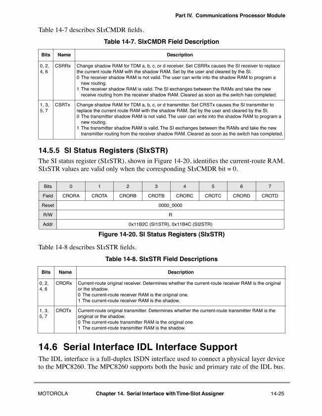
Part IV. Communications Processor Module
Table 14-7 describes SIxCMDR Þelds.
14.5.5 SI Status Registers (SIxSTR)The SI status register (SIxSTR), shown in Figure 14-20, identiÞes the current-route RAM.SIxSTR values are valid only when the corresponding SIxCMDR bit = 0.
Table 14-8 describes SIxSTR Þelds.
14.6 Serial Interface IDL Interface Support The IDL interface is a full-duplex ISDN interface used to connect a physical layer deviceto the MPC8260. The MPC8260 supports both the basic and primary rate of the IDL bus.
Table 14-7. SIxCMDR Field Description
Bits Name Description
0, 2, 4, 6
CSRRx Change shadow RAM for TDM a, b, c, or d receiver. Set CSRRx causes the SI receiver to replace the current route RAM with the shadow RAM. Set by the user and cleared by the SI.0 The receiver shadow RAM is not valid. The user can write into the shadow RAM to program a
new routing.1 The receiver shadow RAM is valid. The SI exchanges between the RAMs and take the new
receive routing from the receiver shadow RAM. Cleared as soon as the switch has completed.
1, 3, 5, 7
CSRTx Change shadow RAM for TDM a, b, c, or d transmitter. Set CRSTx causes the SI transmitter to replace the current route RAM with the shadow RAM. Set by the user and cleared by the SI.0 The transmitter shadow RAM is not valid. The user can write into the shadow RAM to program a
new routing.1 The transmitter shadow RAM is valid. The SI exchanges between the RAMs and take the new
transmitter routing from the receiver shadow RAM. Cleared as soon as the switch has completed.
Bits 0 1 2 3 4 5 6 7
Field CRORA CROTA CRORB CROTB CRORC CROTC CRORD CROTD
Reset 0000_0000
R/W R
Addr 0x11B2C (SI1STR), 0x11B4C (SI2STR)
Figure 14-20. SI Status Registers (SIxSTR)
Table 14-8. SIxSTR Field Descriptions
Bits Name Description
0, 2, 4, 6
CRORx Current-route original receiver. Determines whether the current-route receiver RAM is the original or the shadow. 0 The current-route receiver RAM is the original one.1 The current-route receiver RAM is the shadow.
1, 3, 5, 7
CROTx Current-route original transmitter. Determines whether the current-route transmitter RAM is the original or the shadow. 0 The current-route transmitter RAM is the original one.1 The current-route transmitter RAM is the shadow.
MOTOROLA Chapter 14. Serial Interface with Time-Slot Assigner 14-25
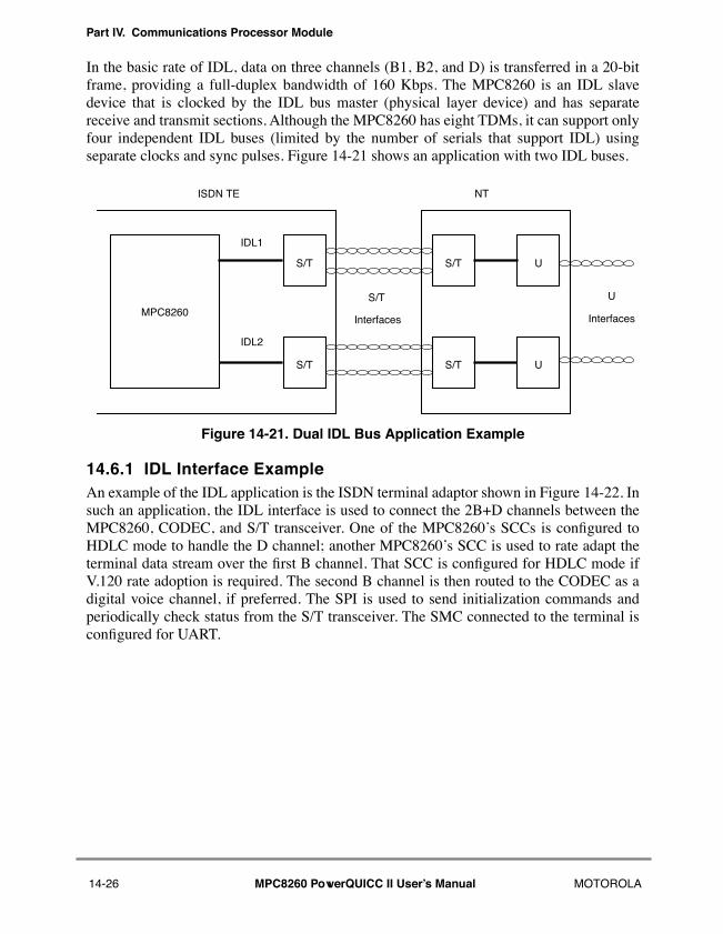
Part IV. Communications Processor Module
In the basic rate of IDL, data on three channels (B1, B2, and D) is transferred in a 20-bitframe, providing a full-duplex bandwidth of 160 Kbps. The MPC8260 is an IDL slavedevice that is clocked by the IDL bus master (physical layer device) and has separatereceive and transmit sections. Although the MPC8260 has eight TDMs, it can support onlyfour independent IDL buses (limited by the number of serials that support IDL) usingseparate clocks and sync pulses. Figure 14-21 shows an application with two IDL buses.
Figure 14-21. Dual IDL Bus Application Example
14.6.1 IDL Interface ExampleAn example of the IDL application is the ISDN terminal adaptor shown in Figure 14-22. Insuch an application, the IDL interface is used to connect the 2B+D channels between theMPC8260, CODEC, and S/T transceiver. One of the MPC8260Õs SCCs is conÞgured toHDLC mode to handle the D channel; another MPC8260Õs SCC is used to rate adapt theterminal data stream over the Þrst B channel. That SCC is conÞgured for HDLC mode ifV.120 rate adoption is required. The second B channel is then routed to the CODEC as adigital voice channel, if preferred. The SPI is used to send initialization commands andperiodically check status from the S/T transceiver. The SMC connected to the terminal isconÞgured for UART.
MPC8260
S/T
S/T
U
U
S/T
S/T
IDL1
S/T
Interfaces
IDL2
ISDN TE NT
U
Interfaces
14-26 MPC8260 PowerQUICC II UserÕs Manual MOTOROLA
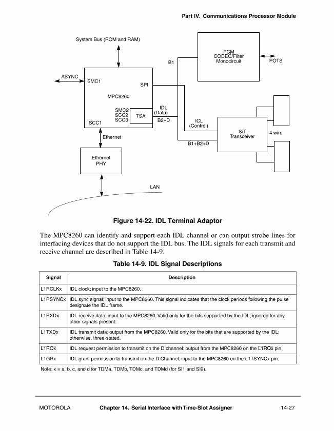
Part IV. Communications Processor Module
Figure 14-22. IDL Terminal Adaptor
The MPC8260 can identify and support each IDL channel or can output strobe lines forinterfacing devices that do not support the IDL bus. The IDL signals for each transmit andreceive channel are described in Table 14-9.
Table 14-9. IDL Signal Descriptions
Signal Description
L1RCLKx IDL clock; input to the MPC8260.
L1RSYNCx IDL sync signal; input to the MPC8260. This signal indicates that the clock periods following the pulse designate the IDL frame.
L1RXDx IDL receive data; input to the MPC8260. Valid only for the bits supported by the IDL; ignored for any other signals present.
L1TXDx IDL transmit data; output from the MPC8260. Valid only for the bits that are supported by the IDL; otherwise, three-stated.
L1RQx IDL request permission to transmit on the D channel; output from the MPC8260 on the L1RQx pin.
L1GRx IDL grant permission to transmit on the D Channel; input to the MPC8260 on the L1TSYNCx pin.
Note: x = a, b, c, and d for TDMa, TDMb, TDMc, and TDMd (for SI1 and SI2).
TSASCC1
Ethernet
EthernetPHY
LAN
ASYNC
PCMCODEC/FilterMonocircuit
S/TTransceiver
SPI
ICL(Control)
B1+B2+D
IDL(Data)
B2+D
B1
MPC8260
System Bus (ROM and RAM)
SMC1
POTS
4 wire
SCC2SMC2
SCC3
MOTOROLA Chapter 14. Serial Interface with Time-Slot Assigner 14-27
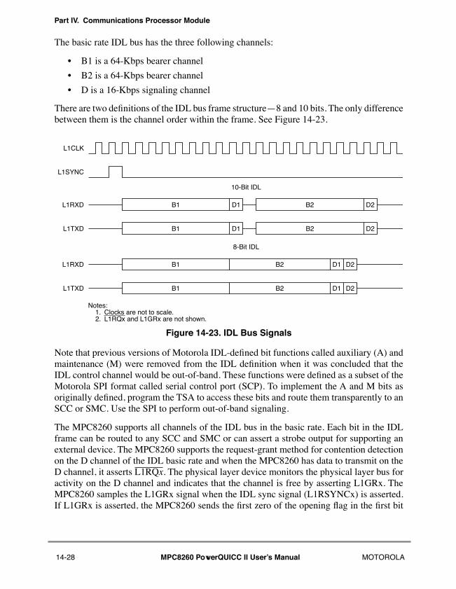
Part IV. Communications Processor Module
The basic rate IDL bus has the three following channels:
¥ B1 is a 64-Kbps bearer channel
¥ B2 is a 64-Kbps bearer channel
¥ D is a 16-Kbps signaling channel
There are two deÞnitions of the IDL bus frame structureÑ8 and 10 bits. The only differencebetween them is the channel order within the frame. See Figure 14-23.
Figure 14-23. IDL Bus Signals
Note that previous versions of Motorola IDL-deÞned bit functions called auxiliary (A) andmaintenance (M) were removed from the IDL deÞnition when it was concluded that theIDL control channel would be out-of-band. These functions were deÞned as a subset of theMotorola SPI format called serial control port (SCP). To implement the A and M bits asoriginally deÞned, program the TSA to access these bits and route them transparently to anSCC or SMC. Use the SPI to perform out-of-band signaling.
The MPC8260 supports all channels of the IDL bus in the basic rate. Each bit in the IDLframe can be routed to any SCC and SMC or can assert a strobe output for supporting anexternal device. The MPC8260 supports the request-grant method for contention detectionon the D channel of the IDL basic rate and when the MPC8260 has data to transmit on theD channel, it asserts L1RQx. The physical layer device monitors the physical layer bus foractivity on the D channel and indicates that the channel is free by asserting L1GRx. TheMPC8260 samples the L1GRx signal when the IDL sync signal (L1RSYNCx) is asserted.If L1GRx is asserted, the MPC8260 sends the Þrst zero of the opening ßag in the Þrst bit
L1CLK
L1SYNC
L1RXD
L1TXD
B1 D1
10-Bit IDL
D2
B1 D1 B2 D2
L1RXD
L1TXD
B1 D1
8-Bit IDL
D2
B1 B2 D2
B2
D1
B2
Notes:1. Clocks are not to scale.2. L1RQx and L1GRx are not shown.
14-28 MPC8260 PowerQUICC II UserÕs Manual MOTOROLA
Part IV. Communications Processor Module
of the D channel. If a collision is detected on the D channel, the physical layer devicenegates L1GRx. The MPC8260 then stops sending and retransmits the frame when L1GRxis reasserted. This procedure is handled automatically for the Þrst two buffers of a frame.
For the primary rate IDL, the MPC8260 supports up to four 8-bit channels in the frame,determined by the SIx RAM programming. To support more channels, the user can routemore than one channel to each SCC and the SCC treats it as one high-speed stream andstore it in the same data buffers (appropriate only for transparent data). Additionally, theMPC8260 can be used to assert strobes for support of additional external IDL channels.
The IDL interface supports the CCITT I.460 recommendation for data-rate adaptation sinceit separately accesses each bit of the IDL bus. The current-route RAM speciÞes which bitsare supported by the IDL interface and by which serial controller. The receiver onlyreceives bits that are enabled by the receiver route RAM. Otherwise, the transmitter sendsonly bits that are enabled by the transmitter route RAM and three-states L1TXDx.
14.6.2 IDL Interface ProgrammingTo program an IDL interface, Þrst program SIxMR[GMx] to the IDL grant mode for thatchannel. If the receive and transmit sections interface to the same IDL bus, setSIxMR[CRTx] to internally connect the Rx clock and sync signals to the transmit section.Then, program the SIx RAM used for the IDL channels to the preferred routing. SeeSection 14.4.4, ÒSIx RAM Programming Example.Ó
DeÞne the IDL frame structure by programming SIxMR[xFSDx] to have a 1-bit delay fromframe sync to data, SIxMR[FEx] to sample on the falling edge, and SIxMR[CEx] to transmiton the rising edge of the clock. Program the parallel I/O open-drain register so that L1TXDxis three-stated when inactive; see Section 35.2.1, ÒPort Open-Drain Registers (PODRAÐPODRD).Ó To support the D channel, program the appropriate CMXSCR[GRx] bit, asdescribed in Section 15.4.5, ÒCMX SCC Clock Route Register (CMXSCR),Ó and programthe SIx RAM entry to route data to the chosen serial controller. The two deÞnitions of IDL,8 or 10 bits, are implemented by simply modifying the SIx RAM programming. In bothcases, L1GRx is sampled with L1TSYNCx and transferred to the D-channel SCC as a grantindication.
MOTOROLA Chapter 14. Serial Interface with Time-Slot Assigner 14-29
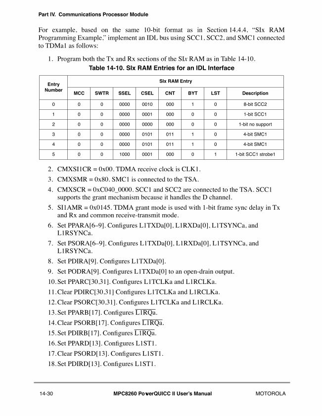
Part IV. Communications Processor Module
For example, based on the same 10-bit format as in Section 14.4.4, ÒSIx RAMProgramming Example,Ó implement an IDL bus using SCC1, SCC2, and SMC1 connectedto TDMa1 as follows:
1. Program both the Tx and Rx sections of the SIx RAM as in Table 14-10.
2. CMXSI1CR = 0x00. TDMA receive clock is CLK1.
3. CMXSMR = 0x80. SMC1 is connected to the TSA.
4. CMXSCR = 0xC040_0000. SCC1 and SCC2 are connected to the TSA. SCC1 supports the grant mechanism because it handles the D channel.
5. SI1AMR = 0x0145. TDMA grant mode is used with 1-bit frame sync delay in Tx and Rx and common receive-transmit mode.
6. Set PPARA[6Ð9]. ConÞgures L1TXDa[0], L1RXDa[0], L1TSYNCa, and L1RSYNCa.
7. Set PSORA[6Ð9]. ConÞgures L1TXDa[0], L1RXDa[0], L1TSYNCa, and L1RSYNCa.
8. Set PDIRA[9]. ConÞgures L1TXDa[0].
9. Set PODRA[9]. ConÞgures L1TXDa[0] to an open-drain output.
10. Set PPARC[30,31]. ConÞgures L1TCLKa and L1RCLKa.
11. Clear PDIRC[30,31] ConÞgures L1TCLKa and L1RCLKa.
12. Clear PSORC[30,31]. ConÞgures L1TCLKa and L1RCLKa.
13. Set PPARB[17]. ConÞgures L1RQa.
14. Clear PSORB[17]. ConÞgures L1RQa.
15. Set PDIRB[17]. ConÞgures L1RQa.
16. Set PPARD[13]. ConÞgures L1ST1.
17. Clear PSORD[13]. ConÞgures L1ST1.
18. Set PDIRD[13]. ConÞgures L1ST1.
Table 14-10. SIx RAM Entries for an IDL Interface
Entry Number
SIx RAM Entry
MCC SWTR SSEL CSEL CNT BYT LST Description
0 0 0 0000 0010 000 1 0 8-bit SCC2
1 0 0 0000 0001 000 0 0 1-bit SCC1
2 0 0 0000 0000 000 0 0 1-bit no support
3 0 0 0000 0101 011 1 0 4-bit SMC1
4 0 0 0000 0101 011 1 0 4-bit SMC1
5 0 0 1000 0001 000 0 1 1-bit SCC1 strobe1
14-30 MPC8260 PowerQUICC II UserÕs Manual MOTOROLA
Part IV. Communications Processor Module
19. SI1CMDR is not used.
20. SI1STR does not need to be read.
21. ConÞgure the SCC1 for HDLC operation (to handle the LAPD protocol of the D channel), and conÞgure SCC2 and SMC1 as preferred.
22. SI1GMR = 0x01. Enable TDM A (one static TDM).
23. Enable SCC1, SCC2 and SMC1.
14.7 Serial Interface GCI SupportThe MPC8260 fully supports the normal mode of the GCI, also known as the ISDN-oriented modular revision 2.2 (IOM-2), and the SCIT. The MPC8260 also supports the D-channel access control in S/T interface terminals using the command/indication (C/I)channel.
The GCI bus consists of four linesÑtwo data lines, a clock, and a frame synchronizationline. Usually, an 8-kHz frame structure deÞnes the various channels within the 256-kbpsdata rate. The MPC8260 supports two (limited by the number of SMCs) independent GCIbuses, each with independent receive and transmit sections. The interface can also be usedin a multiplexed frame structure on which up to eight physical layer devices multiplex theirGCI channels. In this mode, the data rate would be 2,048 kbps.
In the GCI bus, the clock rate is twice the data rate. The SI divides the input clock by twoto produce the data clock. The MPC8260 also has data strobe lines and the 1´ data rateclock L1CLKOx output pins. These signals are used for interfacing devices to GCI that donot support the GCI bus. Table 14-11 describes GCI signals for each transmit and receivechannel.
The GCI bus signals are shown in Figure 14-24.
Table 14-11. GCI Signals
Signal Description
L1RSYNCx Used as a GCI sync signal; input to the MPC8260. This signal indicates that the clock periods following the pulse designate the GCI frame.
L1RCLKx Used as a GCI clock; input to the MPC8260. The L1RCLKx signal frequency is twice the data clock.
L1RXDx Used as a GCI receive data; input to the MPC8260.
L1TXDx Used as a GCI transmit data; open-drain output. Valid only for the bits that are supported by the IDL; otherwise, three-stated.
L1CLKOx Optional signal; output from the MPC8260. This 1´ clock output is used to clock devices that do not interface directly to the GCI. If the double-speed clock is used, (DSCx bit is set in the SIxMR), this output is the L1RCLKx divided by 2; otherwise, it is simply a 1´ output of the L1RCLKx signal.
Note: x = a, b, c, and d for TDMa, TDMb, TDMc, and TDMd (for SI1 and SI2).
MOTOROLA Chapter 14. Serial Interface with Time-Slot Assigner 14-31
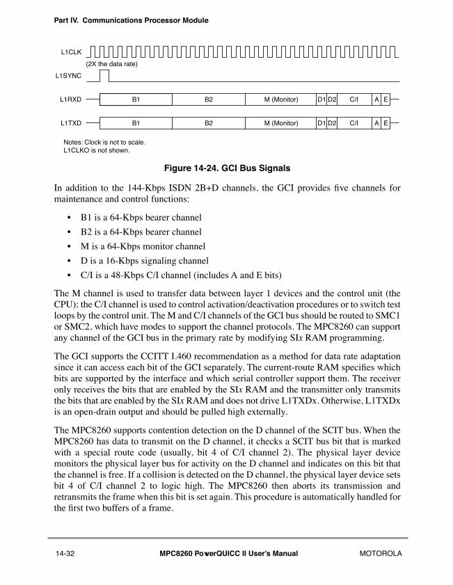
Part IV. Communications Processor Module
Figure 14-24. GCI Bus Signals
In addition to the 144-Kbps ISDN 2B+D channels, the GCI provides Þve channels formaintenance and control functions:
¥ B1 is a 64-Kbps bearer channel
¥ B2 is a 64-Kbps bearer channel
¥ M is a 64-Kbps monitor channel
¥ D is a 16-Kbps signaling channel
¥ C/I is a 48-Kbps C/I channel (includes A and E bits)
The M channel is used to transfer data between layer 1 devices and the control unit (theCPU); the C/I channel is used to control activation/deactivation procedures or to switch testloops by the control unit. The M and C/I channels of the GCI bus should be routed to SMC1or SMC2, which have modes to support the channel protocols. The MPC8260 can supportany channel of the GCI bus in the primary rate by modifying SIx RAM programming.
The GCI supports the CCITT I.460 recommendation as a method for data rate adaptationsince it can access each bit of the GCI separately. The current-route RAM speciÞes whichbits are supported by the interface and which serial controller support them. The receiveronly receives the bits that are enabled by the SIx RAM and the transmitter only transmitsthe bits that are enabled by the SIx RAM and does not drive L1TXDx. Otherwise, L1TXDxis an open-drain output and should be pulled high externally.
The MPC8260 supports contention detection on the D channel of the SCIT bus. When theMPC8260 has data to transmit on the D channel, it checks a SCIT bus bit that is markedwith a special route code (usually, bit 4 of C/I channel 2). The physical layer devicemonitors the physical layer bus for activity on the D channel and indicates on this bit thatthe channel is free. If a collision is detected on the D channel, the physical layer device setsbit 4 of C/I channel 2 to logic high. The MPC8260 then aborts its transmission andretransmits the frame when this bit is set again. This procedure is automatically handled forthe Þrst two buffers of a frame.
L1CLK
L1SYNC
L1RXD
L1TXD
B1 B2
B1 B2 M (Monitor) C/I A E
M (Monitor) C/I A E
(2X the data rate)
Notes: Clock is not to scale.L1CLKO is not shown.
D2D1
D1 D2
14-32 MPC8260 PowerQUICC II UserÕs Manual MOTOROLA
Part IV. Communications Processor Module
14.7.1 SI GCI Activation/Deactivation ProcedureIn the deactivated state, the clock pulse is disabled and the data line is at a logic one. Thelayer 1 device activates the MPC8260 by enabling the clock pulses and by an indication inthe channel 0 C/I channel. The MPC8260 reports to the core (via a maskable interrupt) thata valid indication is in the SMC RxBD.
When the core activates the line, the data output of L1TXDn is programmed to zero bysetting SIxGMR[STZx]. Code 0 (command timing TIM) is transmitted on channel 0 C/Ichannel to the layer 1 device until STZx is reset. The physical layer device resumes theclock pulses and gives an indication in the channel 0 C/I channel. The core should resetSTZx to enable data output.
14.7.2 Serial Interface GCI ProgrammingThe following sections describe serial interface GCI programming.
14.7.2.1 Normal Mode GCI ProgrammingThe user can program and conÞgure the channels used for the GCI bus interface. First, theSIxMR register to the GCI/SCIT mode for that channel must be programmed, using theDSCx, FEx, CEx, and RFSDx bits. This mode deÞnes the sync pulse to GCI sync forframing and data clock as one-half the input clock rate. The user can program more thanone channel to interface to the GCI bus. Also, if the receive and transmit section are usedfor interfacing the same GCI bus, the user internally connects the receive clock and syncsignals to the SIx RAM transmit section, using the CRTx bits. The user should then deÞnethe GCI frame routing and strobe select using the SIx RAM.
When the receive and transmit section uses the same clock and sync signals, these sectionsshould be programmed to the same conÞguration. Also, the L1TXDx pin in the I/O registershould be programmed to be an open-drain output. To support the monitor and the C/Ichannels in GCI, those channels should be routed to one of the SMCs. To support the Dchannel when there is no possibility of collision, the user should clear the SIxMR[GRx] bitcorresponding to the SCC that supports the D channel.
14.7.2.2 SCIT ProgrammingFor interfacing the GCI/SCIT bus, SIxMR must be programmed to the GCI/SCIT mode.The SIx RAM is programmed to support a 96-bit frame length and the frame sync isprogrammed to the GCI sync pulse. Generally, the SCIT bus supports the D channel accesscollision mechanism. For this purpose, the user should program the CRTx bits so thereceive and transmit sections use the same clock and sync signals and program the GRx bitsto transfer the D channel grant to the SCC that supports this channel. The received (grant)bit should be marked by programming the channel select bits of the SIx RAM to 0b0111for an internal assertion of a strobe on this bit. This bit is sampled by the SI and transferredto the D-channel SCC as the grant. The bit is generally bit 4 of the C/I in channel 2 of theGCI, but any other bit can be selected using the SIx RAM.
MOTOROLA Chapter 14. Serial Interface with Time-Slot Assigner 14-33
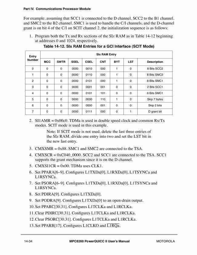
Part IV. Communications Processor Module
For example, assuming that SCC1 is connected to the D channel, SCC2 to the B1 channel,and SMC2 to the B2 channel, SMC1 is used to handle the C/I channels, and the D-channelgrant is on bit 4 of the C/I on SCIT channel 2, the initialization sequence is as follows:
1. Program both the Tx and Rx sections of the SIx RAM as in Table 14-12 beginning at addresses 0 and 1024, respectively.
2. SI1AMR = 0x00c0. TDMa is used in double speed clock and common Rx/Tx modes. SCIT mode is used in this example.
Note: If SCIT mode is not used, delete the last three entries ofthe SIx RAM, divide one entry into two and set the LST bit inthe new last entry.
3. CMXSMR = 0x88. SMC1 and SMC2 are connected to the TSA.
4. CMXSCR = 0xC040_0000. SCC2 and SCC1 are connected to the TSA. SCC1 supports the grant mechanism since it is on the D channel.
5. CMXSI1CR = 0x00. TDMa uses CLK1.
6. Set PPARA[6Ð9]. ConÞgures L1TXDa[0], L1RXDa[0], L1TSYNCa and L1RSYNCa.
7. Set PSORA[6Ð9]. ConÞgures L1TXDa[0], L1RXDa[0], L1TSYNCa and L1RSYNCa.
8. Set PDIRA[9]. ConÞgures L1TXDa[0].
9. Set PODRA[9]. ConÞgures L1TXDa[0] to an open-drain output.
10. Set PPARC[30,31]. ConÞgures L1TCLKa and L1RCLKa.
11. Clear PDIRC[30,31]. ConÞgures L1TCLKa and L1RCLKa.
12. Clear PSORC[30,31]. ConÞgures L1TCLKa and L1RCLKa.
13. Set PPARB[17]. ConÞgures L1CLKO and L1RQa.
Table 14-12. SIx RAM Entries for a GCI Interface (SCIT Mode)
Entry Number
SIx RAM Entry
MCC SWTR SSEL CSEL CNT BYT LST Description
0 0 0 0000 0010 000 1 0 8 Bits SCC2
1 0 0 0000 0110 000 1 0 8 Bits SMC2
2 0 0 0000 0101 000 1 0 8 Bits SMC1
3 0 0 0000 0001 001 0 0 2 Bits SCC1
4 0 0 0000 0101 101 0 0 6 Bits SMC1
5 0 0 0000 0000 110 1 0 Skip 7 bytes
6 0 0 0000 0000 001 0 0 Skip 2 bits
7 0 0 0000 0111 000 0 1 D grant bit
14-34 MPC8260 PowerQUICC II UserÕs Manual MOTOROLA
Part IV. Communications Processor Module
14. Clear PSORB[17]. ConÞgures L1CLKO and L1RQa.
15. Set PDIRB[17]. ConÞgures L1CLKO and L1RQa.
16. If the 1x GCI data clock is required, set PBPAR bit 16 and PBDIR bit 16 and clear PSORB 16, which conÞgures L1CLKOa as an output.
17. ConÞgure SCC1 for HDLC operation (to handle the LAPD protocol of the D channel). ConÞgure SMC1 for SCIT operation and conÞgure SCC2 and SMC2 as preferred.
18. SI1GMR = 0x11. Enable TDMa (one static TDM), STZ for TDMa.
19. SI1CMDR is not used.
20. SI1STR does not need to be read.
21. Enable the SCC1, SCC2, SMC1 and SMC2.
MOTOROLA Chapter 14. Serial Interface with Time-Slot Assigner 14-35

Part IV. Communications Processor Module
14-36 MPC8260 PowerQUICC II UserÕs Manual MOTOROLA
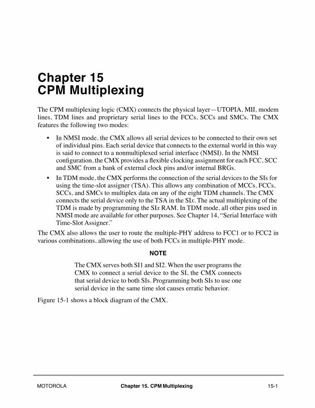
Chapter 15 CPM Multiplexing150150
The CPM multiplexing logic (CMX) connects the physical layerÑUTOPIA, MII, modemlines, TDM lines and proprietary serial lines to the FCCs, SCCs and SMCs. The CMXfeatures the following two modes:
¥ In NMSI mode, the CMX allows all serial devices to be connected to their own set of individual pins. Each serial device that connects to the external world in this way is said to connect to a nonmultiplexed serial interface (NMSI). In the NMSI conÞguration, the CMX provides a ßexible clocking assignment for each FCC, SCC and SMC from a bank of external clock pins and/or internal BRGs.
¥ In TDM mode, the CMX performs the connection of the serial devices to the SIs for using the time-slot assigner (TSA). This allows any combination of MCCs, FCCs, SCCs, and SMCs to multiplex data on any of the eight TDM channels. The CMX connects the serial device only to the TSA in the SIx. The actual multiplexing of the TDM is made by programming the SIx RAM. In TDM mode, all other pins used in NMSI mode are available for other purposes. See Chapter 14, ÒSerial Interface with Time-Slot Assigner.Ó
The CMX also allows the user to route the multiple-PHY address to FCC1 or to FCC2 invarious combinations, allowing the use of both FCCs in multiple-PHY mode.
NOTE
The CMX serves both SI1 and SI2. When the user programs theCMX to connect a serial device to the SI, the CMX connectsthat serial device to both SIs. Programming both SIs to use oneserial device in the same time slot causes erratic behavior.
Figure 15-1 shows a block diagram of the CMX.
MOTOROLA Chapter 15. CPM Multiplexing 15-1
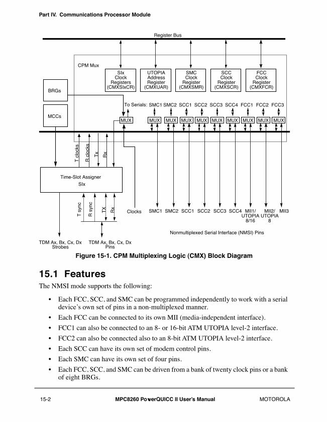
Part IV. Communications Processor Module
Figure 15-1. CPM Multiplexing Logic (CMX) Block Diagram
15.1 FeaturesThe NMSI mode supports the following:
¥ Each FCC, SCC, and SMC can be programmed independently to work with a serial deviceÕs own set of pins in a non-multiplexed manner.
¥ Each FCC can be connected to its own MII (media-independent interface).
¥ FCC1 can also be connected to an 8- or 16-bit ATM UTOPIA level-2 interface.
¥ FCC2 can also be connected also to an 8-bit ATM UTOPIA level-2 interface.
¥ Each SCC can have its own set of modem control pins.
¥ Each SMC can have its own set of four pins.
¥ Each FCC, SCC, and SMC can be driven from a bank of twenty clock pins or a bank of eight BRGs.
Time-Slot Assigner
SIx
R c
lock
s
T c
lock
s
R s
ync
T s
ync
TDM Ax, Bx, Cx, DxPinsStrobes
Register Bus
TDM Ax, Bx, Cx, Dx
Tx
TX SMC1
Nonmultiplexed Serial Interface (NMSI) Pins
Rx
Rx
Clocks
CPM Mux
BRGs
To Serials:
UTOPIAAddressRegister
(CMXUAR)
SMCClock
Register(CMXSMR)
SCCClock
Register(CMXSCR)
FCCClock
Register(CMXFCR)
SIxClock
Registers(CMXSIxCR)
SMC1
MCCsMUX
MII3
FCC3
MUX
MII2/
FCC2
MUX
MII1/
FCC1
MUX
SCC4
SCC4
MUX
SCC3
SCC3
MUX
SCC2
SCC2
MUX
SCC1
SCC1
MUX
SMC2
SMC2
MUX
UTOPIA8/16
UTOPIA8
MUX
15-2 MPC8260 PowerQUICC II UserÕs Manual MOTOROLA
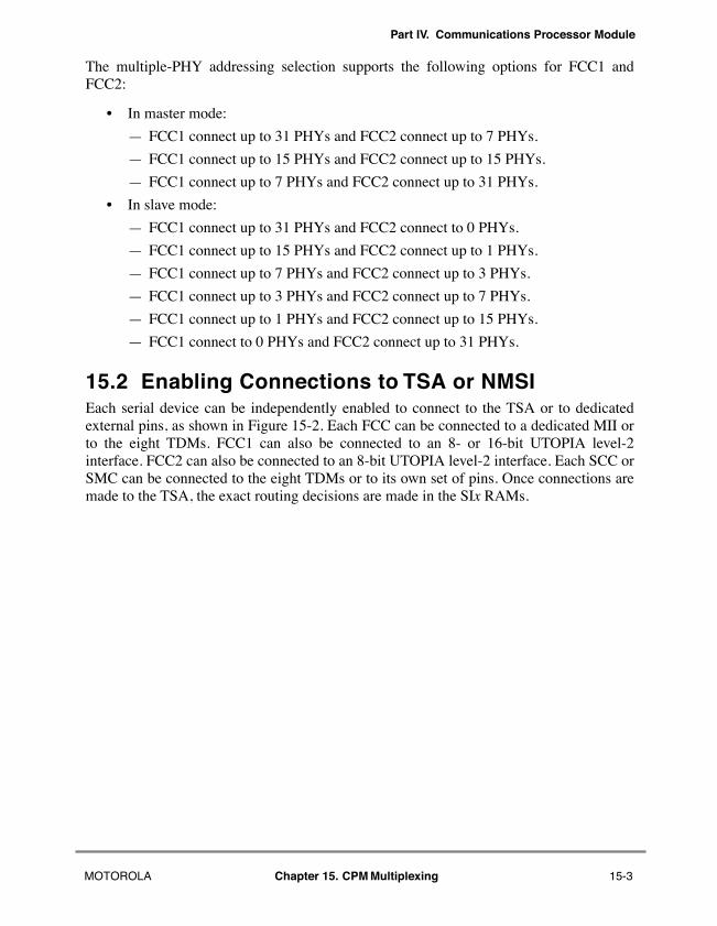
Part IV. Communications Processor Module
The multiple-PHY addressing selection supports the following options for FCC1 andFCC2:
¥ In master mode:
Ñ FCC1 connect up to 31 PHYs and FCC2 connect up to 7 PHYs.
Ñ FCC1 connect up to 15 PHYs and FCC2 connect up to 15 PHYs.
Ñ FCC1 connect up to 7 PHYs and FCC2 connect up to 31 PHYs.
¥ In slave mode:
Ñ FCC1 connect up to 31 PHYs and FCC2 connect to 0 PHYs.
Ñ FCC1 connect up to 15 PHYs and FCC2 connect up to 1 PHYs.
Ñ FCC1 connect up to 7 PHYs and FCC2 connect up to 3 PHYs.
Ñ FCC1 connect up to 3 PHYs and FCC2 connect up to 7 PHYs.
Ñ FCC1 connect up to 1 PHYs and FCC2 connect up to 15 PHYs.
Ñ FCC1 connect to 0 PHYs and FCC2 connect up to 31 PHYs.
15.2 Enabling Connections to TSA or NMSIEach serial device can be independently enabled to connect to the TSA or to dedicatedexternal pins, as shown in Figure 15-2. Each FCC can be connected to a dedicated MII orto the eight TDMs. FCC1 can also be connected to an 8- or 16-bit UTOPIA level-2interface. FCC2 can also be connected to an 8-bit UTOPIA level-2 interface. Each SCC orSMC can be connected to the eight TDMs or to its own set of pins. Once connections aremade to the TSA, the exact routing decisions are made in the SIx RAMs.
MOTOROLA Chapter 15. CPM Multiplexing 15-3
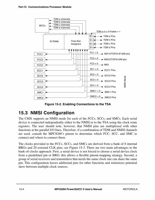
Part IV. Communications Processor Module
Figure 15-2. Enabling Connections to the TSA
15.3 NMSI ConÞgurationThe CMX supports an NMSI mode for each of the FCCs, SCCs, and SMCs. Each serialdevice is connected independently either to the NMSI or to the TSA using the clock routeregisters. The user should note, however, that NMSI pins are multiplexed with otherfunctions at the parallel I/O lines. Therefore, if a combination of TDM and NMSI channelsare used, consult the MPC8260Õs pinout to determine which FCC, SCC, and SMC toconnect and where to connect them.
The clocks provided to the FCCs, SCCs, and SMCs are derived from a bank of 8 internalBRGs and 20 external CLK pins; see Figure 15-3. There are two main advantages to thebank-of-clocks approach. First, a serial device is not forced to choose a serial device clockfrom a predeÞned pin or BRG; this allows a ßexible pinout-mapping strategy. Second, agroup of serial receivers and transmitters that needs the same clock rate can share the samepin. This conÞguration leaves additional pins for other functions and minimizes potentialskew between multiple clock sources.
En
En
En
En
SI RAMs Time-SlotAssigners
TDM a,b,c,d Enable = 1
TDM a Pins
TDM b Pins
TDM c Pins
TDM d Pins
FCC1
FCC2
FCC3
SCC1
SCC2
SCC3
SCC4
SMC1
SMC2
MII1/UTOPIA 8/16/M-phyFC1 = 0
MII2/UTOPIA 8/M-phyFC2 = 0
MII3FC3 = 0
SCC1 PinsSC1 = 0
SCC2 PinsSC2 = 0
SCC3 PinsSC3 = 0
SCC4 PinsSC4 = 0
SMC1 PinsSMC1 = 0
SMC2 PinsSMC2 = 0
MCCs
TDM a channelsTDM b channelsTDM c channelsTDM d channels
NM
SI M
ode
15-4 MPC8260 PowerQUICC II UserÕs Manual MOTOROLA
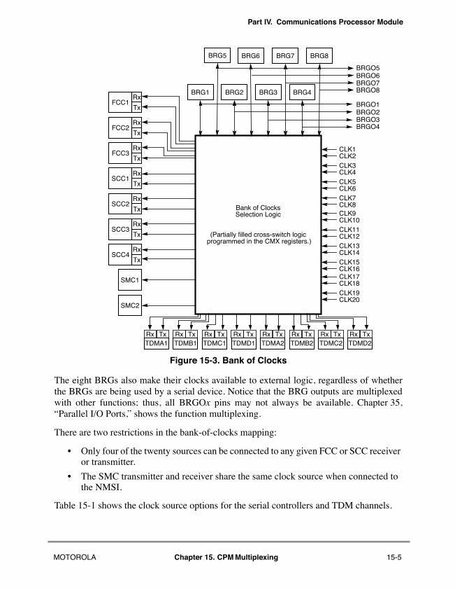
Part IV. Communications Processor Module
Figure 15-3. Bank of Clocks
The eight BRGs also make their clocks available to external logic, regardless of whetherthe BRGs are being used by a serial device. Notice that the BRG outputs are multiplexedwith other functions; thus, all BRGOx pins may not always be available. Chapter 35,ÒParallel I/O Ports,Ó shows the function multiplexing.
There are two restrictions in the bank-of-clocks mapping:
¥ Only four of the twenty sources can be connected to any given FCC or SCC receiver or transmitter.
¥ The SMC transmitter and receiver share the same clock source when connected to the NMSI.
Table 15-1 shows the clock source options for the serial controllers and TDM channels.
BRG1 BRG2 BRG3 BRG4
CLK1CLK2
BRGO1BRGO2BRGO3BRGO4
Bank of ClocksSelection Logic
CLK3CLK4CLK5CLK6CLK7CLK8CLK9CLK10CLK11CLK12CLK13CLK14CLK15CLK16
BRG5 BRG6 BRG7 BRG8
BRGO5BRGO6BRGO7BRGO8
FCC1Tx
CLK17CLK18CLK19CLK20
(Partially filled cross-switch logic programmed in the CMX registers.)
Rx
FCC2Tx
Rx
FCC3Tx
Rx
SCC1Tx
Rx
SCC2Tx
Rx
SCC3Tx
Rx
SCC4Tx
Rx
SMC1
SMC2
TDMA1TxRx
TDMB1TxRx
TDMC1TxRx
TDMD1TxRx
TDMA2TxRx
TDMB2TxRx
TDMC2TxRx
TDMD2TxRx
MOTOROLA Chapter 15. CPM Multiplexing 15-5
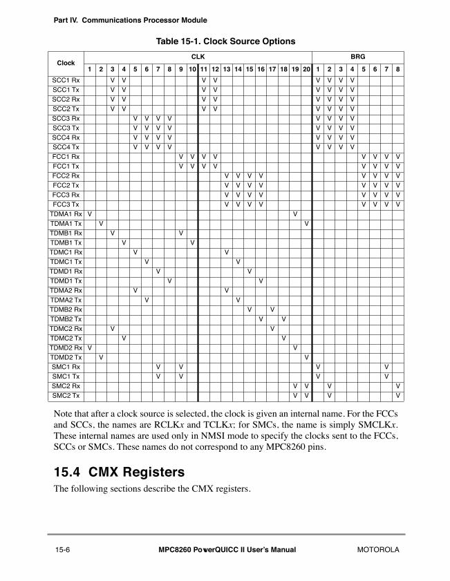
Part IV. Communications Processor Module
Note that after a clock source is selected, the clock is given an internal name. For the FCCsand SCCs, the names are RCLKx and TCLKx; for SMCs, the name is simply SMCLKx.These internal names are used only in NMSI mode to specify the clocks sent to the FCCs,SCCs or SMCs. These names do not correspond to any MPC8260 pins.
15.4 CMX RegistersThe following sections describe the CMX registers.
Table 15-1. Clock Source Options
ClockCLK BRG
1 2 3 4 5 6 7 8 9 10 11 12 13 14 15 16 17 18 19 20 1 2 3 4 5 6 7 8
SCC1 Rx V V V V V V V VSCC1 Tx V V V V V V V VSCC2 Rx V V V V V V V VSCC2 Tx V V V V V V V VSCC3 Rx V V V V V V V VSCC3 Tx V V V V V V V VSCC4 Rx V V V V V V V VSCC4 Tx V V V V V V V VFCC1 Rx V V V V V V V VFCC1 Tx V V V V V V V VFCC2 Rx V V V V V V V VFCC2 Tx V V V V V V V VFCC3 Rx V V V V V V V VFCC3 Tx V V V V V V V V
TDMA1 Rx V VTDMA1 Tx V VTDMB1 Rx V VTDMB1 Tx V VTDMC1 Rx V VTDMC1 Tx V VTDMD1 Rx V VTDMD1 Tx V VTDMA2 Rx V VTDMA2 Tx V VTDMB2 Rx V VTDMB2 Tx V VTDMC2 Rx V VTDMC2 Tx V VTDMD2 Rx V VTDMD2 Tx V VSMC1 Rx V V V VSMC1 Tx V V V VSMC2 Rx V V V VSMC2 Tx V V V V
15-6 MPC8260 PowerQUICC II UserÕs Manual MOTOROLA
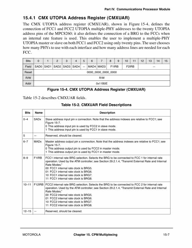
Part IV. Communications Processor Module
15.4.1 CMX UTOPIA Address Register (CMXUAR)The CMX UTOPIA address register (CMXUAR), shown in Figure 15-4, deÞnes theconnection of FCC1 and FCC2 UTOPIA multiple-PHY addresses to the twenty UTOPIAaddress pins of the MPC8260; it also deÞnes the connection of a BRG to the FCCs whenan internal rate feature is used. This enables the user to implement a multiple-PHYUTOPIA master or slave on both FCC1 and FCC2 using only twenty pins. The user chooseshow many PHYs to use with each interface and how many address lines are needed for eachFCC.
Table 15-2 describes CMXUAR Þelds.
Bits 0 1 2 3 4 5 6 7 8 9 10 11 12 13 14 15
Field SAD0 SAD1 SAD2 SAD3 SAD4 Ñ MAD4 MAD3 F1IRB F2IRB Ñ
Reset 0000_0000_0000_0000
R/W R/W
Addr 0x11B0E
Figure 15-4. CMX UTOPIA Address Register (CMXUAR)
Table 15-2. CMXUAR Field Descriptions
Bits Name Description
0Ð4 SADx Slave address input pin x connection. Note that the address indexes are relative to FCC1; see Figure 15-7.0 This address input pin is used by FCC2 in slave mode.1 This address input pin is used by FCC1 in slave mode.
5 Ñ Reserved, should be cleared.
6Ð7 MADx Master address output pin x connection. Note that the address indexes are relative to FCC1; see Figure 15-7.0 This address output pin is used by FCC2 in master mode.1 This address output pin is used by FCC1 in master mode.
8Ð9 F1IRB FCC1 internal rate BRG selection. Selects the BRG to be connected to FCC 1 for internal rate operation. Used by the ATM controller; see Section 29.2.1.4, ÒTransmit External Rate and Internal Rate Modes.Ó00 FCC1 internal rate clock is BRG5.01 FCC1 internal rate clock is BRG6.10 FCC1 internal rate clock is BRG7.11 FCC1 internal rate clock is BRG8.
10Ð11 F12IRB FCC2 internal rate BRG selection. Selects the BRG to be connected to FCC 2 for internal rate operation. Used by the ATM controller; see Section 29.2.1.4, ÒTransmit External Rate and Internal Rate Modes.Ó00 FCC2 internal rate clock is BRG5.01 FCC2 internal rate clock is BRG6.10 FCC2 internal rate clock is BRG7.11 FCC2 internal rate clock is BRG8.
12Ð15 Ñ Reserved, should be cleared.
MOTOROLA Chapter 15. CPM Multiplexing 15-7
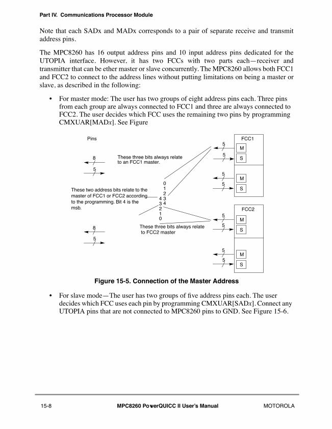
Part IV. Communications Processor Module
Note that each SADx and MADx corresponds to a pair of separate receive and transmitaddress pins.
The MPC8260 has 16 output address pins and 10 input address pins dedicated for theUTOPIA interface. However, it has two FCCs with two parts eachÑreceiver andtransmitter that can be ether master or slave concurrently. The MPC8260 allows both FCC1and FCC2 to connect to the address lines without putting limitations on being a master orslave, as described in the following:
¥ For master mode: The user has two groups of eight address pins each. Three pins from each group are always connected to FCC1 and three are always connected to FCC2. The user decides which FCC uses the remaining two pins by programming CMXUAR[MADx]. See Figure
Figure 15-5. Connection of the Master Address
¥ For slave modeÑThe user has two groups of Þve address pins each. The user decides which FCC uses each pin by programming CMXUAR[SADx]. Connect any UTOPIA pins that are not connected to MPC8260 pins to GND. See Figure 15-6.
FCC1
FCC2
M
S
M
S
M
S
M
S
5
5
5
5
5
5
5
5
8
5
8
5
01234
43210
These three bits always relate
These three bits always relate to FCC2 master
Pins
to an FCC1 master.
These two address bits relate to the master of FCC1 or FCC2 according to the programming. Bit 4 is the msb.
15-8 MPC8260 PowerQUICC II UserÕs Manual MOTOROLA
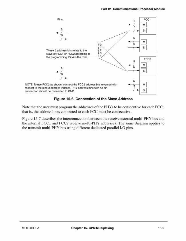
Part IV. Communications Processor Module
Figure 15-6. Connection of the Slave Address
Note that the user must program the addresses of the PHYs to be consecutive for each FCC; that is, the address lines connected to each FCC must be consecutive.
Figure 15-7 describes the interconnection between the receive external multi-PHY bus andthe internal FCC1 and FCC2 receive multi-PHY addresses. The same diagram applies tothe transmit multi-PHY bus using different dedicated parallel I/O pins.
FCC1
FCC2
M
S
M
S
M
S
M
S
5
5
5
5
5
5
5
5
8
5
8
5
01234
43210
Pins
These 5 address bits relate to the slave of FCC1 or FCC2 according to the programming. Bit 4 is the msb.
NOTE: To use FCC2 as shown, connect the FCC2 address bits reversed with respect to the pinout address indexes. PHY address pins with no pin connection should be connected to GND.
MOTOROLA Chapter 15. CPM Multiplexing 15-9
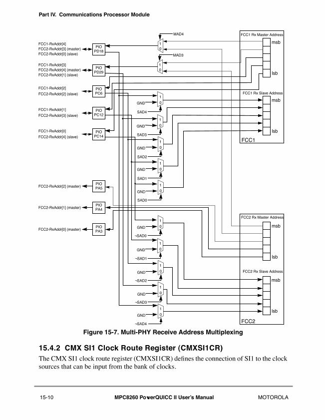
Part IV. Communications Processor Module
Figure 15-7. Multi-PHY Receive Address Multiplexing
15.4.2 CMX SI1 Clock Route Register (CMXSI1CR)The CMX SI1 clock route register (CMXSI1CR) deÞnes the connection of SI1 to the clocksources that can be input from the bank of clocks.
1
0
ÂSAD4
1
0
ÂSAD3
1
0
ÂSAD2
1
0
ÂSAD1
1
0
ÂSAD0
1
0
SAD0
1
0
SAD1
1
0
SAD2
1
0
SAD3
1
0
SAD4
10
MAD4
10
MAD3
FCC1 Rx Master Address
msb
lsb
FCC1 Rx Slave Address
msb
lsb
FCC2 Rx Slave Address
msb
lsb
FCC2 Rx Master Address
msb
lsb
FCC1-RxAddr[4]
GND
GND
GND
GND
GND
GND
GND
GND
GND
GND
FCC1
FCC2
PIOPA4
PIOPD18
PIOPD29
PIOPC6
PIOPC12
PIOPC14
PIOPA5
PIOPA3
FCC2-RxAddr[3] (master)FCC2-RxAddr[0] (slave)
FCC1-RxAddr[3]FCC2-RxAddr[4] (master)FCC2-RxAddr[1] (slave)
FCC1-RxAddr[2]
FCC2-RxAddr[2] (slave)
FCC1-RxAddr[1]
FCC2-RxAddr[3] (slave)
FCC1-RxAddr[0]
FCC2-RxAddr[4] (slave)
FCC2-RxAddr[2] (master)
FCC2-RxAddr[1] (master)
FCC2-RxAddr[0] (master)
15-10 MPC8260 PowerQUICC II UserÕs Manual MOTOROLA
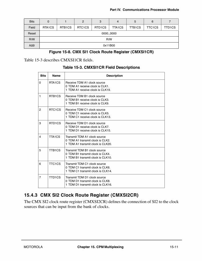
Part IV. Communications Processor Module
Table 15-3 describes CMXSI1CR Þelds.
15.4.3 CMX SI2 Clock Route Register (CMXSI2CR)The CMX SI2 clock route register (CMXSI2CR) deÞnes the connection of SI2 to the clocksources that can be input from the bank of clocks.
Bits 0 1 2 3 4 5 6 7
Field RTA1CS RTB1CS RTC1CS RTD1CS TTA1CS TTB1CS TTC1CS TTD1CS
Reset 0000_0000
R/W R/W
Addr 0x11B00
Figure 15-8. CMX SI1 Clock Route Register (CMXSI1CR)
Table 15-3. CMXSI1CR Field Descriptions
Bits Name Description
0 RTA1CS Receive TDM A1 clock source0 TDM A1 receive clock is CLK1.1 TDM A1 receive clock is CLK19.
1 RTB1CS Receive TDM B1 clock source0 TDM B1 receive clock is CLK3.1 TDM B1 receive clock is CLK9.
2 RTC1CS Receive TDM C1 clock source0 TDM C1 receive clock is CLK5.1 TDM C1 receive clock is CLK13.
3 RTD1CS Receive TDM D1 clock source0 TDM D1 receive clock is CLK7.1 TDM D1 receive clock is CLK15.
4 TTA1CS Transmit TDM A1 clock source0 TDM A1 transmit clock is CLK2.1 TDM A1 transmit clock is CLK20.
5 TTB1CS Transmit TDM B1 clock source0 TDM B1 transmit clock is CLK4.1 TDM B1 transmit clock is CLK10.
6 TTC1CS Transmit TDM C1 clock source0 TDM C1 transmit clock is CLK6.1 TDM C1 transmit clock is CLK14.
7 TTD1CS Transmit TDM D1 clock source0 TDM D1 transmit clock is CLK8.1 TDM D1 transmit clock is CLK16.
MOTOROLA Chapter 15. CPM Multiplexing 15-11
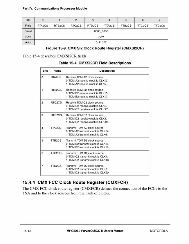
Part IV. Communications Processor Module
Table 15-4 describes CMXSI2CR Þelds.
15.4.4 CMX FCC Clock Route Register (CMXFCR)The CMX FCC clock route register (CMXFCR) deÞnes the connection of the FCCs to theTSA and to the clock sources from the bank of clocks.
Bits 0 1 2 3 4 5 6 7
Field RTA2CS RTB2CS RTC2CS RTD2CS TTA2CS TTB2CS TTC2CS TTD2CS
Reset 0000_0000
R/W R/W
Addr 0x11B02
Figure 15-9. CMX SI2 Clock Route Register (CMXSI2CR)
Table 15-4. CMXSI2CR Field Descriptions
Bits Name Description
0 RTA2CS Receive TDM A2 clock source0 TDM A2 receive clock is CLK13.1 TDM A2 receive clock is CLK5.
1 RTB2CS Receive TDM B2 clock source0 TDM B2 receive clock is CLK15.1 TDM B2 receive clock is CLK17.
2 RTC2CS Receive TDM C2 clock source0 TDM C2 receive clock is CLK3.1 TDM C2 receive clock is CLK17.
3 RTD2CS Receive TDM D2 clock source0 TDM D2 receive clock is CLK1.1 TDM D2 receive clock is CLK19.
4 TTA2CS Transmit TDM A2 clock source0 TDM A2 transmit clock is CLK14.1 TDM A2 transmit clock is CLK6.
5 TTB2CS Transmit TDM B2 clock source0 TDM B2 transmit clock is CLK16.1 TDM B2 transmit clock is CLK18.
6 TTC2CS Transmit TDM C2 clock source0 TDM C2 transmit clock is CLK4.1 TDM C2 transmit clock is CLK18.
7 TTD2CS Transmit TDM D2 clock source0 TDM D2 transmit clock is CLK2.1 TDM D2 transmit clock is CLK20.
15-12 MPC8260 PowerQUICC II UserÕs Manual MOTOROLA
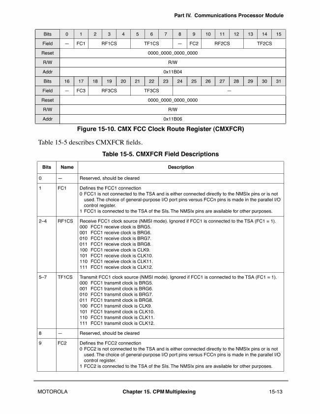
Part IV. Communications Processor Module
Table 15-5 describes CMXFCR Þelds.
Bits 0 1 2 3 4 5 6 7 8 9 10 11 12 13 14 15
Field Ñ FC1 RF1CS TF1CS Ñ FC2 RF2CS TF2CS
Reset 0000_0000_0000_0000
R/W R/W
Addr 0x11B04
Bits 16 17 18 19 20 21 22 23 24 25 26 27 28 29 30 31
Field Ñ FC3 RF3CS TF3CS Ñ
Reset 0000_0000_0000_0000
R/W R/W
Addr 0x11B06
Figure 15-10. CMX FCC Clock Route Register (CMXFCR)
Table 15-5. CMXFCR Field Descriptions
Bits Name Description
0 Ñ Reserved, should be cleared
1 FC1 DeÞnes the FCC1 connection0 FCC1 is not connected to the TSA and is either connected directly to the NMSIx pins or is not
used. The choice of general-purpose I/O port pins versus FCCn pins is made in the parallel I/O control register.
1 FCC1 is connected to the TSA of the SIs. The NMSIx pins are available for other purposes.
2Ð4 RF1CS Receive FCC1 clock source (NMSI mode). Ignored if FCC1 is connected to the TSA (FC1 = 1).000 FCC1 receive clock is BRG5.001 FCC1 receive clock is BRG6.010 FCC1 receive clock is BRG7.011 FCC1 receive clock is BRG8.100 FCC1 receive clock is CLK9.101 FCC1 receive clock is CLK10.110 FCC1 receive clock is CLK11.111 FCC1 receive clock is CLK12.
5Ð7 TF1CS Transmit FCC1 clock source (NMSI mode). Ignored if FCC1 is connected to the TSA (FC1 = 1).000 FCC1 transmit clock is BRG5.001 FCC1 transmit clock is BRG6.010 FCC1 transmit clock is BRG7.011 FCC1 transmit clock is BRG8.100 FCC1 transmit clock is CLK9.101 FCC1 transmit clock is CLK10.110 FCC1 transmit clock is CLK11.111 FCC1 transmit clock is CLK12.
8 Ñ Reserved, should be cleared
9 FC2 DeÞnes the FCC2 connection0 FCC2 is not connected to the TSA and is either connected directly to the NMSIx pins or is not
used. The choice of general-purpose I/O port pins versus FCCn pins is made in the parallel I/O control register.
1 FCC2 is connected to the TSA of the SIs. The NMSIx pins are available for other purposes.
MOTOROLA Chapter 15. CPM Multiplexing 15-13
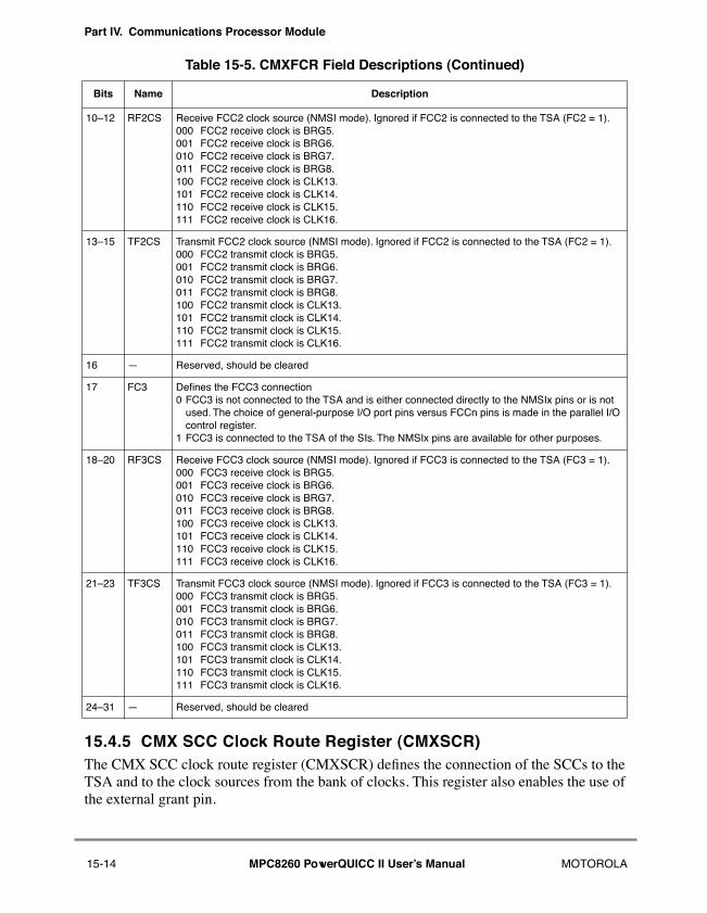
Part IV. Communications Processor Module
15.4.5 CMX SCC Clock Route Register (CMXSCR)The CMX SCC clock route register (CMXSCR) deÞnes the connection of the SCCs to theTSA and to the clock sources from the bank of clocks. This register also enables the use ofthe external grant pin.
10Ð12 RF2CS Receive FCC2 clock source (NMSI mode). Ignored if FCC2 is connected to the TSA (FC2 = 1).000 FCC2 receive clock is BRG5.001 FCC2 receive clock is BRG6.010 FCC2 receive clock is BRG7.011 FCC2 receive clock is BRG8.100 FCC2 receive clock is CLK13.101 FCC2 receive clock is CLK14.110 FCC2 receive clock is CLK15.111 FCC2 receive clock is CLK16.
13Ð15 TF2CS Transmit FCC2 clock source (NMSI mode). Ignored if FCC2 is connected to the TSA (FC2 = 1).000 FCC2 transmit clock is BRG5.001 FCC2 transmit clock is BRG6.010 FCC2 transmit clock is BRG7.011 FCC2 transmit clock is BRG8.100 FCC2 transmit clock is CLK13.101 FCC2 transmit clock is CLK14.110 FCC2 transmit clock is CLK15.111 FCC2 transmit clock is CLK16.
16 Ñ Reserved, should be cleared
17 FC3 DeÞnes the FCC3 connection0 FCC3 is not connected to the TSA and is either connected directly to the NMSIx pins or is not
used. The choice of general-purpose I/O port pins versus FCCn pins is made in the parallel I/O control register.
1 FCC3 is connected to the TSA of the SIs. The NMSIx pins are available for other purposes.
18Ð20 RF3CS Receive FCC3 clock source (NMSI mode). Ignored if FCC3 is connected to the TSA (FC3 = 1).000 FCC3 receive clock is BRG5.001 FCC3 receive clock is BRG6.010 FCC3 receive clock is BRG7.011 FCC3 receive clock is BRG8.100 FCC3 receive clock is CLK13.101 FCC3 receive clock is CLK14.110 FCC3 receive clock is CLK15.111 FCC3 receive clock is CLK16.
21Ð23 TF3CS Transmit FCC3 clock source (NMSI mode). Ignored if FCC3 is connected to the TSA (FC3 = 1).000 FCC3 transmit clock is BRG5.001 FCC3 transmit clock is BRG6.010 FCC3 transmit clock is BRG7.011 FCC3 transmit clock is BRG8.100 FCC3 transmit clock is CLK13.101 FCC3 transmit clock is CLK14.110 FCC3 transmit clock is CLK15.111 FCC3 transmit clock is CLK16.
24Ð31 Ñ Reserved, should be cleared
Table 15-5. CMXFCR Field Descriptions (Continued)
Bits Name Description
15-14 MPC8260 PowerQUICC II UserÕs Manual MOTOROLA
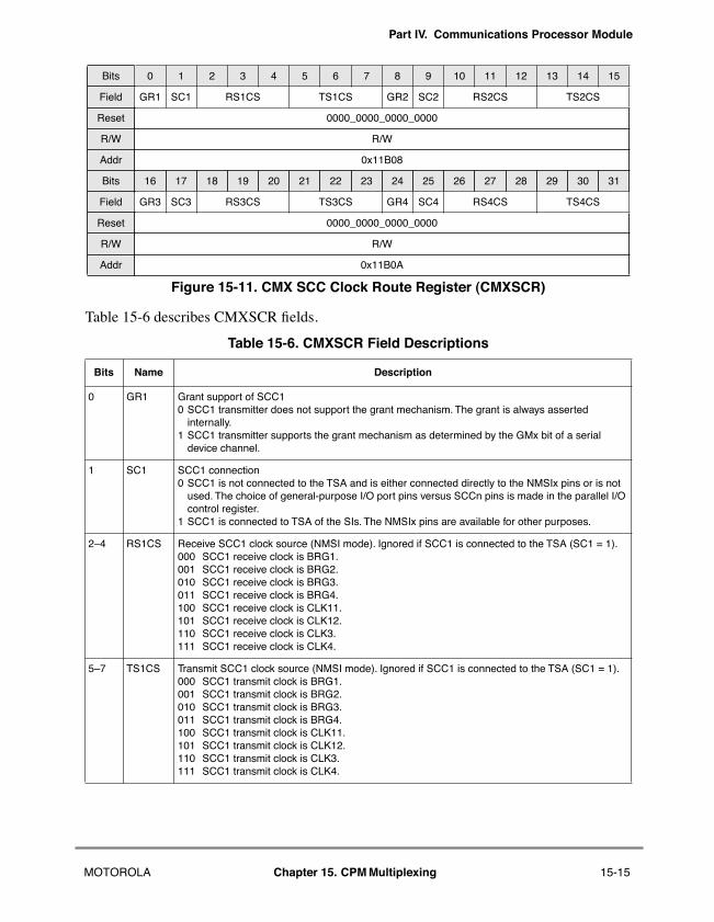
Part IV. Communications Processor Module
Table 15-6 describes CMXSCR Þelds.
Bits 0 1 2 3 4 5 6 7 8 9 10 11 12 13 14 15
Field GR1 SC1 RS1CS TS1CS GR2 SC2 RS2CS TS2CS
Reset 0000_0000_0000_0000
R/W R/W
Addr 0x11B08
Bits 16 17 18 19 20 21 22 23 24 25 26 27 28 29 30 31
Field GR3 SC3 RS3CS TS3CS GR4 SC4 RS4CS TS4CS
Reset 0000_0000_0000_0000
R/W R/W
Addr 0x11B0A
Figure 15-11. CMX SCC Clock Route Register (CMXSCR)
Table 15-6. CMXSCR Field Descriptions
Bits Name Description
0 GR1 Grant support of SCC10 SCC1 transmitter does not support the grant mechanism. The grant is always asserted
internally.1 SCC1 transmitter supports the grant mechanism as determined by the GMx bit of a serial
device channel.
1 SC1 SCC1 connection0 SCC1 is not connected to the TSA and is either connected directly to the NMSIx pins or is not
used. The choice of general-purpose I/O port pins versus SCCn pins is made in the parallel I/O control register.
1 SCC1 is connected to TSA of the SIs. The NMSIx pins are available for other purposes.
2Ð4 RS1CS Receive SCC1 clock source (NMSI mode). Ignored if SCC1 is connected to the TSA (SC1 = 1).000 SCC1 receive clock is BRG1.001 SCC1 receive clock is BRG2.010 SCC1 receive clock is BRG3.011 SCC1 receive clock is BRG4.100 SCC1 receive clock is CLK11.101 SCC1 receive clock is CLK12.110 SCC1 receive clock is CLK3.111 SCC1 receive clock is CLK4.
5Ð7 TS1CS Transmit SCC1 clock source (NMSI mode). Ignored if SCC1 is connected to the TSA (SC1 = 1).000 SCC1 transmit clock is BRG1.001 SCC1 transmit clock is BRG2.010 SCC1 transmit clock is BRG3.011 SCC1 transmit clock is BRG4.100 SCC1 transmit clock is CLK11.101 SCC1 transmit clock is CLK12.110 SCC1 transmit clock is CLK3.111 SCC1 transmit clock is CLK4.
MOTOROLA Chapter 15. CPM Multiplexing 15-15
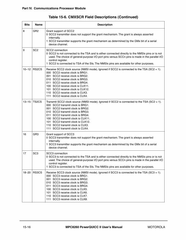
Part IV. Communications Processor Module
8 GR2 Grant support of SCC20 SCC2 transmitter does not support the grant mechanism. The grant is always asserted
internally.1 SCC2 transmitter supports the grant mechanism as determined by the GMx bit of a serial
device channel.
9 SC2 SCC2 connection0 SCC2 is not connected to the TSA and is either connected directly to the NMSIx pins or is not
used. The choice of general-purpose I/O port pins versus SCCn pins is made in the parallel I/O control register.
1 SCC2 is connected to TSA of the SIs. The NMSIx pins are available for other purposes.
10Ð12 RS2CS Receive SCC2 clock source (NMSI mode). Ignored if SCC2 is connected to the TSA (SC2 = 1).000 SCC2 receive clock is BRG1.001 SCC2 receive clock is BRG2.010 SCC2 receive clock is BRG3.011 SCC2 receive clock is BRG4.100 SCC2 receive clock is CLK11.101 SCC2 receive clock is CLK12.110 SCC2 receive clock is CLK3.111 SCC2 receive clock is CLK4.
13Ð15 TS2CS Transmit SCC2 clock source (NMSI mode). Ignored if SCC2 is connected to the TSA (SC2 = 1).000 SCC2 transmit clock is BRG1.001 SCC2 transmit clock is BRG2.010 SCC2 transmit clock is BRG3.011 SCC2 transmit clock is BRG4.100 SCC2 transmit clock is CLK11.101 SCC2 transmit clock is CLK12.110 SCC2 transmit clock is CLK3.111 SCC2 transmit clock is CLK4.
16 GR3 Grant support of SCC30 SCC3 transmitter does not support the grant mechanism. The grant is always asserted
internally.1 SCC3 transmitter supports the grant mechanism as determined by the GMx bit of a serial
device channel.
17 SC3 SCC3 connection0 SCC3 is not connected to the TSA and is either connected directly to the NMSIx pins or is not
used. The choice of general-purpose I/O port pins versus SCCn pins is made in the parallel I/O control register.
1 SCC3 is connected to TSA of the SIs. The NMSIx pins are available for other purposes.
18Ð20 RS3CS Receive SCC3 clock source (NMSI mode). Ignored if SCC3 is connected to the TSA (SC3 = 1).000 SCC3 receive clock is BRG1.001 SCC3 receive clock is BRG2.010 SCC3 receive clock is BRG3.011 SCC3 receive clock is BRG4.100 SCC3 receive clock is CLK5.101 SCC3 receive clock is CLK6.110 SCC3 receive clock is CLK7.111 SCC3 receive clock is CLK8.
Table 15-6. CMXSCR Field Descriptions (Continued)
Bits Name Description
15-16 MPC8260 PowerQUICC II UserÕs Manual MOTOROLA
Part IV. Communications Processor Module
15.4.6 CMX SMC Clock Route Register (CMXSMR)The CMX SMC clock route register (CMXSMR) deÞnes the connection of the SMCs to theTSA and to the clock sources from the bank of clocks.
21Ð23 TS3CS Transmit SCC3 clock source (NMSI mode). Ignored if SCC3 is connected to the TSA (SC3 = 1).000 SCC3 transmit clock is BRG1.001 SCC3 transmit clock is BRG2.010 SCC3 transmit clock is BRG3.011 SCC3 transmit clock is BRG4.100 SCC3 transmit clock is CLK5.101 SCC3 transmit clock is CLK6.110 SCC3 transmit clock is CLK7.111 SCC3 transmit clock is CLK8.
24 GR4 Grant support of SCC40 SCC4 transmitter does not support the grant mechanism. The grant is always asserted
internally.1 SCC4 transmitter supports the grant mechanism as determined by the GMx bit of a serial
device channel.
25 SC4 SCC4 connection0 SCC4 is not connected to the TSA and is either connected directly to the NMSIx pins or is not
used. The choice of general-purpose I/O port pins versus SCCn pins is made in the parallel I/O control register.
1 SCC4 is connected to TSA of the SIs. The NMSIx pins are available for other purposes.
26Ð28 RS4CS Receive SCC4 clock source (NMSI mode). Ignored if SCC4 is connected to the TSA (SC4 = 1).000 SCC4 receive clock is BRG1.001 SCC4 receive clock is BRG2.010 SCC4 receive clock is BRG3.011 SCC4 receive clock is BRG4.100 SCC4 receive clock is CLK5.101 SCC4 receive clock is CLK6.110 SCC4 receive clock is CLK7.111 SCC4 receive clock is CLK8
29Ð31 TS4CS Transmit SCC4 clock source (NMSI mode). Ignored if SCC4 is connected to the TSA (SC4 = 1).000 SCC4 transmit clock is BRG1.001 SCC4 transmit clock is BRG2.010 SCC4 transmit clock is BRG3.011 SCC4 transmit clock is BRG4.100 SCC4 transmit clock is CLK5.101 SCC4 transmit clock is CLK6.110 SCC4 transmit clock is CLK7.111 SCC4 transmit clock is CLK8
Table 15-6. CMXSCR Field Descriptions (Continued)
Bits Name Description
MOTOROLA Chapter 15. CPM Multiplexing 15-17
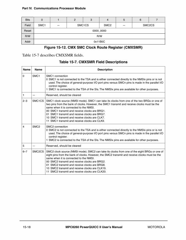
Part IV. Communications Processor Module
Table 15-7 describes CMXSMR Þelds.
Bits 0 1 2 3 4 5 6 7
Field SMC1 Ñ SMC1CS SMC2 Ñ SMC2CS
Reset 0000_0000
R/W R/W
Addr 0x11B0C
Figure 15-12. CMX SMC Clock Route Register (CMXSMR)
Table 15-7. CMXSMR Field Descriptions
Name Name Description
0 SMC1 SMC1 connection0 SMC1 is not connected to the TSA and is either connected directly to the NMSIx pins or is not
used. The choice of general-purpose I/O port pins versus SMCn pins is made in the parallel I/O control register.
1 SMC1 is connected to the TSA of the SIs. The NMSIx pins are available for other purposes.
1 Ñ Reserved, should be cleared
2Ð3 SMC1CS SMC1 clock source (NMSI mode). SMC1 can take its clocks from one of the two BRGs or one of two pins from the bank of clocks. However, the SMC1 transmit and receive clocks must be the same when it is connected to the NMSI. 00 SMC1 transmit and receive clocks are BRG1.01 SMC1 transmit and receive clocks are BRG7.10 SMC1 transmit and receive clocks are CLK7.11 SMC1 transmit and receive clocks are CLK9.
4 SMC2 SMC2 connection0 SMC2 is not connected to the TSA and is either connected directly to the NMSIx pins or is not
used. The choice of general-purpose I/O port pins versus SMCn pins is made in the parallel I/O control register.
1 SMC2 is connected to the TSA of the SIs. The NMSIx pins are available for other purposes.
5 Ñ Reserved, should be cleared
6Ð7 SMC2CS SMC2 clock source (NMSI mode). SMC2 can take its clocks from one of the eight BRGs or one of eight pins from the bank of clocks. However, the SMC2 transmit and receive clocks must be the same when it is connected to the NMSI. 00 SMC2 transmit and receive clocks are BRG2.01 SMC2 transmit and receive clocks are BRG8.10 SMC2 transmit and receive clocks are CLK19.11 SMC2 transmit and receive clocks are CLK20.
15-18 MPC8260 PowerQUICC II UserÕs Manual MOTOROLA
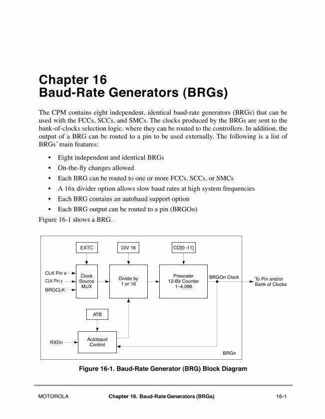
Chapter 16 Baud-Rate Generators (BRGs)160160
The CPM contains eight independent, identical baud-rate generators (BRGs) that can beused with the FCCs, SCCs, and SMCs. The clocks produced by the BRGs are sent to thebank-of-clocks selection logic, where they can be routed to the controllers. In addition, theoutput of a BRG can be routed to a pin to be used externally. The following is a list ofBRGsÕ main features:
¥ Eight independent and identical BRGs
¥ On-the-ßy changes allowed
¥ Each BRG can be routed to one or more FCCs, SCCs, or SMCs
¥ A 16x divider option allows slow baud rates at high system frequencies
¥ Each BRG contains an autobaud support option
¥ Each BRG output can be routed to a pin (BRGOn)
Figure 16-1 shows a BRG.
Figure 16-1. Baud-Rate Generator (BRG) Block Diagram
CLK Pin x ClockSourceMUX
Divide by1 or 16
Prescaler12-Bit Counter
1Ð4,096
DIV 16 CD[0Ð11]
BRGOn Clock
BRGCLK
EXTC
ATB
AutobaudControlRXDn
To Pin and/orBank of Clocks
BRGn
CLK Pin y
MOTOROLA Chapter 16. Baud-Rate Generators (BRGs) 16-1
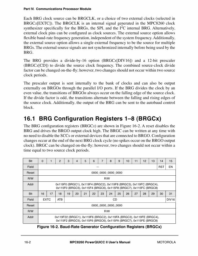
Part IV. Communications Processor Module
Each BRG clock source can be BRGCLK, or a choice of two external clocks (selected inBRGCx[EXTC]). The BRGCLK is an internal signal generated in the MPC8260 clocksynthesizer speciÞcally for the BRGs, the SPI, and the I2C internal BRG. Alternatively,external clock pins can be conÞgured as clock sources. The external source option allowsßexible baud-rate frequency generation, independent of the system frequency. Additionally,the external source option allows a single external frequency to be the source for multipleBRGs. The external source signals are not synchronized internally before being used by theBRG.
The BRG provides a divide-by-16 option (BRGCx[DIV16]) and a 12-bit prescaler(BRGCx[CD]) to divide the source clock frequency. The combined source-clock dividefactor can be changed on-the-ßy; however, two changes should not occur within two sourceclock periods.
The prescaler output is sent internally to the bank of clocks and can also be outputexternally on BRGOn through the parallel I/O ports. If the BRG divides the clock by aneven value, the transitions of BRGOn always occur on the falling edge of the source clock.If the divide factor is odd, the transitions alternate between the falling and rising edges ofthe source clock. Additionally, the output of the BRG can be sent to the autobaud controlblock.
16.1 BRG ConÞguration Registers 1Ð8 (BRGCx)The BRG conÞguration registers (BRGCx) are shown in Figure 16-2. A reset disables theBRG and drives the BRGO output clock high. The BRGC can be written at any time withno need to disable the SCCs or external devices that are connected to BRGO. ConÞgurationchanges occur at the end of the next BRG clock cycle (no spikes occur on the BRGO outputclock). BRGC can be changed on-the-ßy; however, two changes should not occur within atime equal to two source clock periods.
Bit 0 1 2 3 4 5 6 7 8 9 10 11 12 13 14 15
Field Ñ RST EN
Reset 0000_0000_0000_0000
R/W R/W
Addr 0x119F0 (BRGC1), 0x119F4 (BRGC2), 0x119F8 (BRGC3), 0x119FC (BRGC4), 0x115F0 (BRGC5), 0x115F4 (BRGC6), 0x115F8 (BRGC7), 0x115FC (BRGC8)
Bit 16 17 18 19 20 21 22 23 24 25 26 27 28 29 30 31
Field EXTC ATB CD DIV16
Reset 0000_0000_0000_0000
R/W R/W
Addr 0x119F22 (BRGC1), 0x119F6 (BRGC2), 0x119FA (BRGC3), 0x119FE (BRGC4), 0x115F2 (BRGC5), 0x115F6 (BRGC6), 0x115FA (BRGC7), 0x115FE (BRGC8)
Figure 16-2. Baud-Rate Generator Configuration Registers (BRGCx)
16-2 MPC8260 PowerQUICC II UserÕs Manual MOTOROLA
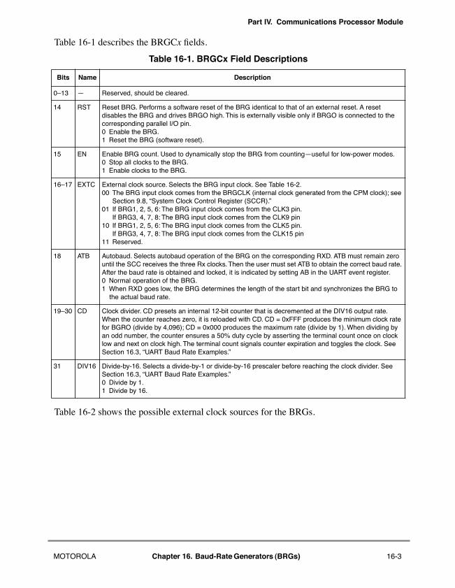
Part IV. Communications Processor Module
Table 16-1 describes the BRGCx Þelds.
Table 16-2 shows the possible external clock sources for the BRGs.
Table 16-1. BRGCx Field Descriptions
Bits Name Description
0Ð13 Ñ Reserved, should be cleared.
14 RST Reset BRG. Performs a software reset of the BRG identical to that of an external reset. A reset disables the BRG and drives BRGO high. This is externally visible only if BRGO is connected to the corresponding parallel I/O pin.0 Enable the BRG.1 Reset the BRG (software reset).
15 EN Enable BRG count. Used to dynamically stop the BRG from countingÑuseful for low-power modes.0 Stop all clocks to the BRG.1 Enable clocks to the BRG.
16Ð17 EXTC External clock source. Selects the BRG input clock. See Table 16-2.00 The BRG input clock comes from the BRGCLK (internal clock generated from the CPM clock); see
Section 9.8, ÒSystem Clock Control Register (SCCR).Ó01 If BRG1, 2, 5, 6: The BRG input clock comes from the CLK3 pin.
If BRG3, 4, 7, 8: The BRG input clock comes from the CLK9 pin10 If BRG1, 2, 5, 6: The BRG input clock comes from the CLK5 pin.
If BRG3, 4, 7, 8: The BRG input clock comes from the CLK15 pin11 Reserved.
18 ATB Autobaud. Selects autobaud operation of the BRG on the corresponding RXD. ATB must remain zero until the SCC receives the three Rx clocks. Then the user must set ATB to obtain the correct baud rate. After the baud rate is obtained and locked, it is indicated by setting AB in the UART event register.0 Normal operation of the BRG.1 When RXD goes low, the BRG determines the length of the start bit and synchronizes the BRG to
the actual baud rate.
19Ð30 CD Clock divider. CD presets an internal 12-bit counter that is decremented at the DIV16 output rate. When the counter reaches zero, it is reloaded with CD. CD = 0xFFF produces the minimum clock rate for BGRO (divide by 4,096); CD = 0x000 produces the maximum rate (divide by 1). When dividing by an odd number, the counter ensures a 50% duty cycle by asserting the terminal count once on clock low and next on clock high. The terminal count signals counter expiration and toggles the clock. See Section 16.3, ÒUART Baud Rate Examples.Ó
31 DIV16 Divide-by-16. Selects a divide-by-1 or divide-by-16 prescaler before reaching the clock divider. See Section 16.3, ÒUART Baud Rate Examples.Ó0 Divide by 1.1 Divide by 16.
MOTOROLA Chapter 16. Baud-Rate Generators (BRGs) 16-3
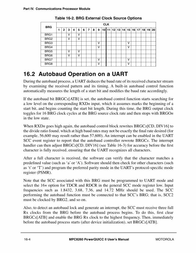
Part IV. Communications Processor Module
16.2 Autobaud Operation on a UARTDuring the autobaud process, a UART deduces the baud rate of its received character streamby examining the received pattern and its timing. A built-in autobaud control functionautomatically measures the length of a start bit and modiÞes the baud rate accordingly.
If the autobaud bit BRGCx[ATB] is set, the autobaud control function starts searching fora low level on the corresponding RXDn input, which it assumes marks the beginning of astart bit, and begins counting the start bit length. During this time, the BRG output clocktoggles for 16 BRG clock cycles at the BRG source clock rate and then stops with BRGOnin the low state.
When RXDn goes high again, the autobaud control block rewrites BRGCx[CD, DIV16] tothe divide ratio found, which at high baud rates may not be exactly the Þnal rate desired (forexample, 56,600 may result rather than 57,600). An interrupt can be enabled in the UARTSCC event register to report that the autobaud controller rewrote BRGCx. The interrupthandler can then adjust BRGCx[CD, DIV16] (see Table 16-3) for accuracy before the Þrstcharacter is fully received, ensuring that the UART recognizes all characters.
After a full character is received, the software can verify that the character matches apredeÞned value (such as ÔaÕ or ÔAÕ). Software should then check for other characters (suchas ÔtÕ or ÔTÕ) and program the preferred parity mode in the UARTÕs protocol-speciÞc moderegister (PSMR).
Note that the SCC associated with this BRG must be programmed to UART mode andselect the 16´ option for TDCR and RDCR in the general SCC mode register low. Inputfrequencies such as 1.8432, 3.68, 7.36, and 14.72 MHz should be used. The SCCperforming the autobaud function must be connected to that SCCÕs BRG; that is, SCC2must be clocked by BRG2, and so on.
Also, to detect an autobaud lock and generate an interrupt, the SCC must receive three fullRx clocks from the BRG before the autobaud process begins. To do this, Þrst clearBRGCx[ATB] and enable the BRG Rx clock to the highest frequency. Then, immediatelybefore the autobaud process starts (after device initialization), set BRGCx[ATB].
Table 16-2. BRG External Clock Source Options
BRGCLK
1 2 3 4 5 6 7 8 9 10 11 12 13 14 15 16 17 18 19 20
BRG1 V VBRG2 V VBRG3 V VBRG4 V VBRG5 V VBRG6 V VBRG7 V VBRG8 V V
16-4 MPC8260 PowerQUICC II UserÕs Manual MOTOROLA
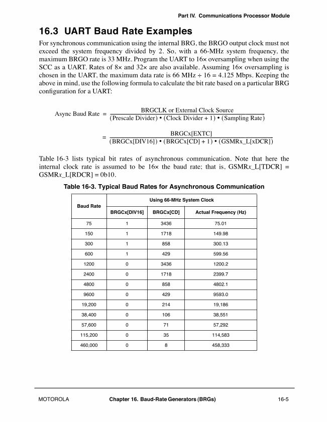
Part IV. Communications Processor Module
16.3 UART Baud Rate Examples For synchronous communication using the internal BRG, the BRGO output clock must notexceed the system frequency divided by 2. So, with a 66-MHz system frequency, themaximum BRGO rate is 33 MHz. Program the UART to 16´ oversampling when using theSCC as a UART. Rates of 8´ and 32´ are also available. Assuming 16´ oversampling ischosen in the UART, the maximum data rate is 66 MHz Ö 16 = 4.125 Mbps. Keeping theabove in mind, use the following formula to calculate the bit rate based on a particular BRGconÞguration for a UART:
Table 16-3 lists typical bit rates of asynchronous communication. Note that here theinternal clock rate is assumed to be 16´ the baud rate; that is, GSMRx_L[TDCR] =GSMRx_L[RDCR] = 0b10.
Table 16-3. Typical Baud Rates for Asynchronous Communication
Baud RateUsing 66-MHz System Clock
BRGCx[DIV16] BRGCx[CD] Actual Frequency (Hz)
75 1 3436 75.01
150 1 1718 149.98
300 1 858 300.13
600 1 429 599.56
1200 0 3436 1200.2
2400 0 1718 2399.7
4800 0 858 4802.1
9600 0 429 9593.0
19,200 0 214 19,186
38,400 0 106 38,551
57,600 0 71 57,292
115,200 0 35 114,583
460,000 0 8 458,333
Async Baud Rate BRGCLK or External Clock SourcePrescale Divider( ) Clock Divider + 1( ) Sampling Rate( )··
-------------------------------------------------------------------------------------------------------------------------------------------------=
BRGCx[EXTC]BRGCx[DIV16]( ) BRGCx[CD] + 1( ) GSMRx_L[xDCR]( )··
---------------------------------------------------------------------------------------------------------------------------------------------------------=
MOTOROLA Chapter 16. Baud-Rate Generators (BRGs) 16-5
Part IV. Communications Processor Module
For synchronous communication, the internal clock is identical to the baud-rate output. Toget the preferred rate, select the system clock according to the following:
For example, to get a rate of 64 kbps, the system clock can be 24.96 MHz,BRGCx[DIV16] = 0, and BRGCx[CD] = 389.
Sync Baud Rate BRGCLK or External Clock SourcePrescale Divider( ) Clock Divider + 1( )·
--------------------------------------------------------------------------------------------------=
BRGCx[EXTC]BRGCx[DIV16]( ) BRGCx[CD] + 1( )·
------------------------------------------------------------------------------------------------=
16-6 MPC8260 PowerQUICC II UserÕs Manual MOTOROLA
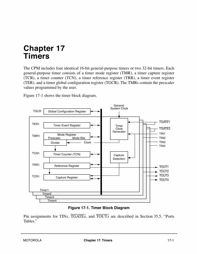
Chapter 17 Timers170170
The CPM includes four identical 16-bit general-purpose timers or two 32-bit timers. Eachgeneral-purpose timer consists of a timer mode register (TMR), a timer capture register(TCR), a timer counter (TCN), a timer reference register (TRR), a timer event register(TER), and a timer global conÞguration register (TGCR). The TMRs contain the prescalervalues programmed by the user.
Figure 17-1 shows the timer block diagram.
Figure 17-1. Timer Block Diagram
Pin assignments for TINx, TGATEx, and TOUTx are described in Section 35.5, ÒPortsTables.Ó
Timer
CaptureDetection
Timer Event Register
Mode RegisterMode BitsPrescaler
Timer Counter (TCN)
Capture Register
Reference Register
Divider Clock
TER1
TMR1
TCN1
TRR1
TCR1
General
TIN1
TOUT1
Timer1Timer2
Timer3Timer4
Global Configuration Register
TGATE1
TGATE2
TGCR
TIN2
TIN3TIN4
TOUT2TOUT3
TOUT4
System Clock
ClockGenerator
MOTOROLA Chapter 17. Timers 17-1

Part IV. Communications Processor Module
17.1 FeaturesThe key features of the timer include the following:
¥ The maximum input clock is the bus clock
¥ Maximum period of 4 seconds (at 66 MHz)
¥ 16-nanosecond resolution (at 66 MHz)
¥ Programmable sources for the clock input
¥ Input capture capability
¥ Output compare with programmable mode for the output pin
¥ Two timers cascade internally or externally to form a 32-bit timer
¥ Free run and restart modes
¥ Functional compatibility with timers on the MC68360 and MPC860
17.2 General-Purpose Timer UnitsThe clock input to the prescaler can be selected from three sources:
¥ The bus clock (CLKIN)
¥ The bus clock divided by 16 (CLKIN/16)
¥ The corresponding TINx, programmed in the parallel port registers
The general system clock is generated in the clock synthesizer and defaults to the systemfrequency. However, the general system clock has the option to be divided before it leavesthe clock synthesizer. This mode, called slow go, is used to save power. Whatever theresulting frequency of the general system clock, the user can either choose that frequencyor the frequency divided by 16 as the input to the prescaler of each timer. Alternatively, theuser may prefer TINx to be the clock source. TINx is internally synchronized to the internalclock. If the user has chosen to internally cascade two 16-bit timers to a 32-bit timer, thena timer can use the clock generated by the output of another timer.
The clock input source is selected by the corresponding TMR[ICLK] bits. The prescaler isprogrammed to divide the clock input by values from 1 to 256 and the output of theprescaler is used as an input to the 16-bit counter. The best resolution of the timer is oneclock cycle (16 ns at 66 MHz). The maximum period (when the reference value is all ones)is 268,435,456 cycles (4 seconds at 66 MHz).
Each timer can be conÞgured to count until a reference is reached and then either begin anew time count immediately or continue to run. The FRR bit of the corresponding TMRselects each mode. Upon reaching the reference value, the corresponding TER bit is set andan interrupt is issued if TMR[ORI] = 1. The timers can output a signal on the timer outputs(TOUT1ÐTOUT4) when the reference value is reached (selected by the correspondingTMR[OM]). This signal can be an active-low pulse or a toggle of the current output. The
17-2 MPC8260 PowerQUICC II UserÕs Manual MOTOROLA
Part IV. Communications Processor Module
output can also be connected internally to the input of another timer, resulting in a 32-bittimer.
In addition, each timer has a 16-bit TCR used to latch the value of the counter when adeÞned transition of TIN1, TIN2, TIN3, or TIN4 is sensed by the corresponding inputcapture edge detector. The type of transition triggering the capture is selected by thecorresponding TMR[CE] bits. Upon a capture or reference event, the corresponding TERbit is set and a maskable interrupt request is issued to the interrupt controller. The timersmay be gated/restarted by an external gate signal. There are two gate signalsÑTGATE1controls timer 1 and/or 2 and TGATE2 controls timer 3 and/or 4. Normal gate mode enablesthe count on a falling edge of TGATEx and disables the count on the rising edge ofTGATEx. This mode allows the timer to count conditionally, based on the state of TGATEx.
The restart gate mode performs the same function as normal mode, except it also resets thecounter on the falling edge of TGATEx. This mode has applications in pulse intervalmeasurement and bus monitoring as follows:
¥ Pulse measurementÑThe restart gate mode can measure a low TGATEx. The rising edge of TGATEx completes the measurement and if TGATEx is connected externally to TINx, it causes the timer to capture the count value and generate a rising-edge interrupt.
¥ Bus monitoringÑThe restart gate mode can detect a signal that is abnormally stuck low. The bus signal should be connected to TGATEx. The timer count is reset on the falling edge of the bus signal and if the bus signal does not go high again within the number of user-deÞned clocks, an interrupt can be generated.
The gate function is enabled in the TMR; the gate operating mode is selected in the TGCR.
NOTETGATEx is internally synchronized to the system clock. IfTGATEx meets the asynchronous input setup time, the counterbegins counting after one system clock when working with theinternal clock.
17.2.1 Cascaded ModeIn this mode, two 16-bit timers can be internally cascaded to form a 32-bit counter. Timer1 may be internally cascaded to timer 2, and timer 3 can be internally cascaded to timer 4.Because the decision to cascade timers is made independently, the user can select two 16-bit timers or one 32-bit timer. TGCR is used to put the timers into cascaded mode, as shownin Figure 17-2.
MOTOROLA Chapter 17. Timers 17-3
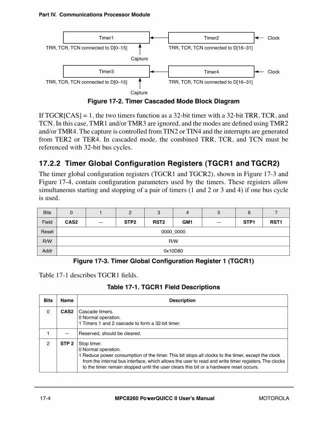
Part IV. Communications Processor Module
Figure 17-2. Timer Cascaded Mode Block Diagram
If TGCR[CAS] = 1, the two timers function as a 32-bit timer with a 32-bit TRR, TCR, andTCN. In this case, TMR1 and/or TMR3 are ignored, and the modes are deÞned using TMR2and/or TMR4. The capture is controlled from TIN2 or TIN4 and the interrupts are generatedfrom TER2 or TER4. In cascaded mode, the combined TRR, TCR, and TCN must bereferenced with 32-bit bus cycles.
17.2.2 Timer Global ConÞguration Registers (TGCR1 and TGCR2)The timer global conÞguration registers (TGCR1 and TGCR2), shown in Figure 17-3 andFigure 17-4, contain conÞguration parameters used by the timers. These registers allowsimultaneous starting and stopping of a pair of timers (1 and 2 or 3 and 4) if one bus cycleis used.
Table 17-1 describes TGCR1 Þelds.
Bits 0 1 2 3 4 5 6 7
Field CAS2 Ñ STP2 RST2 GM1 Ñ STP1 RST1
Reset 0000_0000
R/W R/W
Addr 0x10D80
Figure 17-3. Timer Global Configuration Register 1 (TGCR1)
Table 17-1. TGCR1 Field Descriptions
Bits Name Description
0 CAS2 Cascade timers. 0 Normal operation. 1 Timers 1 and 2 cascade to form a 32-bit timer.
1 Ñ Reserved, should be cleared.
2 STP 2 Stop timer. 0 Normal operation. 1 Reduce power consumption of the timer. This bit stops all clocks to the timer, except the clock
from the internal bus interface, which allows the user to read and write timer registers. The clocks to the timer remain stopped until the user clears this bit or a hardware reset occurs.
Timer1 Timer2
Timer3 Timer4
Capture
Capture
Clock
Clock
TRR, TCR, TCN connected to D[16Ð31] TRR, TCR, TCN connected to D[0Ð15]
TRR, TCR, TCN connected to D[0Ð15] TRR, TCR, TCN connected to D[16Ð31]
17-4 MPC8260 PowerQUICC II UserÕs Manual MOTOROLA
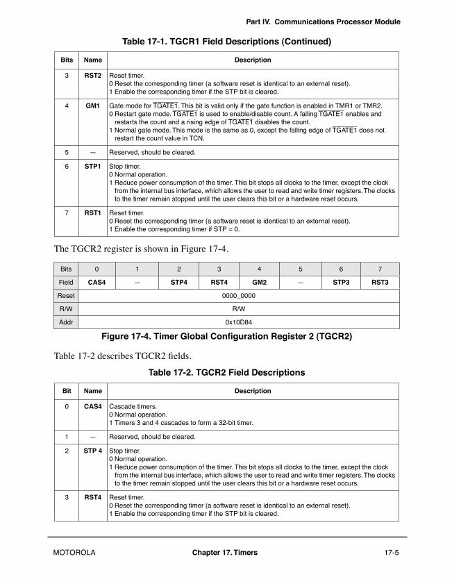
Part IV. Communications Processor Module
The TGCR2 register is shown in Figure 17-4.
Table 17-2 describes TGCR2 Þelds.
3 RST2 Reset timer. 0 Reset the corresponding timer (a software reset is identical to an external reset). 1 Enable the corresponding timer if the STP bit is cleared.
4 GM1 Gate mode for TGATE1. This bit is valid only if the gate function is enabled in TMR1 or TMR2.0 Restart gate mode. TGATE1 is used to enable/disable count. A falling TGATE1 enables and
restarts the count and a rising edge of TGATE1 disables the count.1 Normal gate mode. This mode is the same as 0, except the falling edge of TGATE1 does not
restart the count value in TCN.
5 Ñ Reserved, should be cleared.
6 STP1 Stop timer. 0 Normal operation. 1 Reduce power consumption of the timer. This bit stops all clocks to the timer, except the clock
from the internal bus interface, which allows the user to read and write timer registers. The clocks to the timer remain stopped until the user clears this bit or a hardware reset occurs.
7 RST1 Reset timer. 0 Reset the corresponding timer (a software reset is identical to an external reset). 1 Enable the corresponding timer if STP = 0.
Bits 0 1 2 3 4 5 6 7
Field CAS4 Ñ STP4 RST4 GM2 Ñ STP3 RST3
Reset 0000_0000
R/W R/W
Addr 0x10D84
Figure 17-4. Timer Global Configuration Register 2 (TGCR2)
Table 17-2. TGCR2 Field Descriptions
Bit Name Description
0 CAS4 Cascade timers. 0 Normal operation. 1 Timers 3 and 4 cascades to form a 32-bit timer.
1 Ñ Reserved, should be cleared.
2 STP 4 Stop timer. 0 Normal operation. 1 Reduce power consumption of the timer. This bit stops all clocks to the timer, except the clock
from the internal bus interface, which allows the user to read and write timer registers. The clocks to the timer remain stopped until the user clears this bit or a hardware reset occurs.
3 RST4 Reset timer. 0 Reset the corresponding timer (a software reset is identical to an external reset). 1 Enable the corresponding timer if the STP bit is cleared.
Table 17-1. TGCR1 Field Descriptions (Continued)
Bits Name Description
MOTOROLA Chapter 17. Timers 17-5
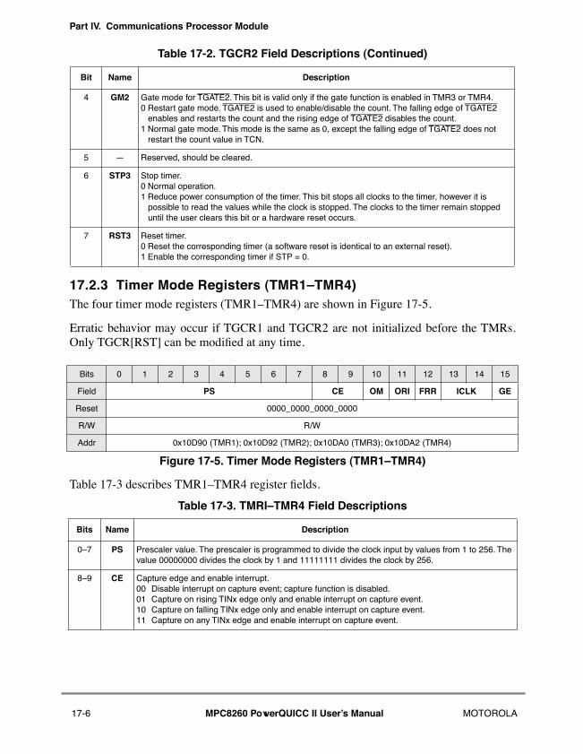
Part IV. Communications Processor Module
17.2.3 Timer Mode Registers (TMR1ÐTMR4)The four timer mode registers (TMR1ÐTMR4) are shown in Figure 17-5.
Erratic behavior may occur if TGCR1 and TGCR2 are not initialized before the TMRs.Only TGCR[RST] can be modiÞed at any time.
Table 17-3 describes TMR1ÐTMR4 register Þelds.
4 GM2 Gate mode for TGATE2. This bit is valid only if the gate function is enabled in TMR3 or TMR4.0 Restart gate mode. TGATE2 is used to enable/disable the count. The falling edge of TGATE2
enables and restarts the count and the rising edge of TGATE2 disables the count.1 Normal gate mode. This mode is the same as 0, except the falling edge of TGATE2 does not
restart the count value in TCN.
5 Ñ Reserved, should be cleared.
6 STP3 Stop timer. 0 Normal operation. 1 Reduce power consumption of the timer. This bit stops all clocks to the timer, however it is
possible to read the values while the clock is stopped. The clocks to the timer remain stopped until the user clears this bit or a hardware reset occurs.
7 RST3 Reset timer. 0 Reset the corresponding timer (a software reset is identical to an external reset). 1 Enable the corresponding timer if STP = 0.
Bits 0 1 2 3 4 5 6 7 8 9 10 11 12 13 14 15
Field PS CE OM ORI FRR ICLK GE
Reset 0000_0000_0000_0000
R/W R/W
Addr 0x10D90 (TMR1); 0x10D92 (TMR2); 0x10DA0 (TMR3); 0x10DA2 (TMR4)
Figure 17-5. Timer Mode Registers (TMR1ÐTMR4)
Table 17-3. TMRIÐTMR4 Field Descriptions
Bits Name Description
0Ð7 PS Prescaler value. The prescaler is programmed to divide the clock input by values from 1 to 256. The value 00000000 divides the clock by 1 and 11111111 divides the clock by 256.
8Ð9 CE Capture edge and enable interrupt. 00 Disable interrupt on capture event; capture function is disabled. 01 Capture on rising TINx edge only and enable interrupt on capture event. 10 Capture on falling TINx edge only and enable interrupt on capture event. 11 Capture on any TINx edge and enable interrupt on capture event.
Table 17-2. TGCR2 Field Descriptions (Continued)
Bit Name Description
17-6 MPC8260 PowerQUICC II UserÕs Manual MOTOROLA
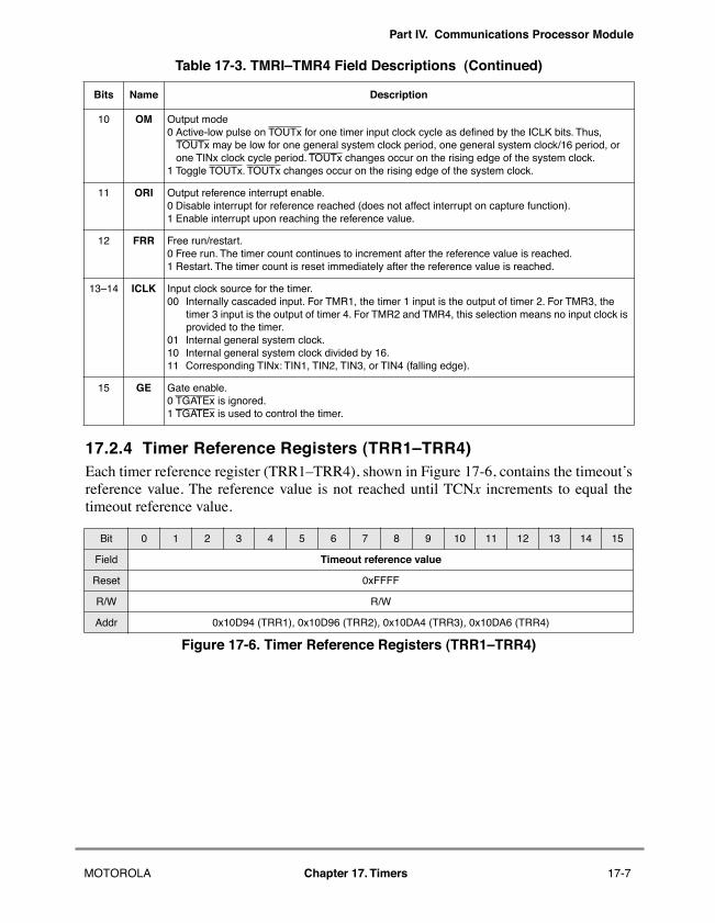
Part IV. Communications Processor Module
17.2.4 Timer Reference Registers (TRR1ÐTRR4)Each timer reference register (TRR1ÐTRR4), shown in Figure 17-6, contains the timeoutÕsreference value. The reference value is not reached until TCNx increments to equal thetimeout reference value.
10 OM Output mode0 Active-low pulse on TOUTx for one timer input clock cycle as deÞned by the ICLK bits. Thus,
TOUTx may be low for one general system clock period, one general system clock/16 period, or one TINx clock cycle period. TOUTx changes occur on the rising edge of the system clock.
1 Toggle TOUTx. TOUTx changes occur on the rising edge of the system clock.
11 ORI Output reference interrupt enable.0 Disable interrupt for reference reached (does not affect interrupt on capture function). 1 Enable interrupt upon reaching the reference value.
12 FRR Free run/restart. 0 Free run. The timer count continues to increment after the reference value is reached. 1 Restart. The timer count is reset immediately after the reference value is reached.
13Ð14 ICLK Input clock source for the timer. 00 Internally cascaded input. For TMR1, the timer 1 input is the output of timer 2. For TMR3, the
timer 3 input is the output of timer 4. For TMR2 and TMR4, this selection means no input clock is provided to the timer.
01 Internal general system clock. 10 Internal general system clock divided by 16. 11 Corresponding TINx: TIN1, TIN2, TIN3, or TIN4 (falling edge).
15 GE Gate enable. 0 TGATEx is ignored.1 TGATEx is used to control the timer.
Bit 0 1 2 3 4 5 6 7 8 9 10 11 12 13 14 15
Field Timeout reference value
Reset 0xFFFF
R/W R/W
Addr 0x10D94 (TRR1), 0x10D96 (TRR2), 0x10DA4 (TRR3), 0x10DA6 (TRR4)
Figure 17-6. Timer Reference Registers (TRR1ÐTRR4)
Table 17-3. TMRIÐTMR4 Field Descriptions (Continued)
Bits Name Description
MOTOROLA Chapter 17. Timers 17-7
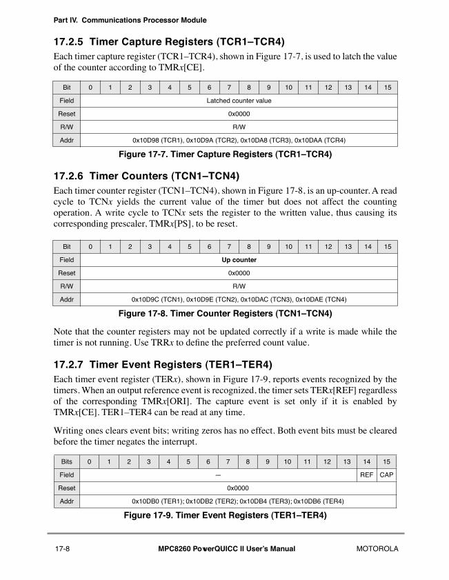
Part IV. Communications Processor Module
17.2.5 Timer Capture Registers (TCR1ÐTCR4)Each timer capture register (TCR1ÐTCR4), shown in Figure 17-7, is used to latch the valueof the counter according to TMRx[CE].
17.2.6 Timer Counters (TCN1ÐTCN4)Each timer counter register (TCN1ÐTCN4), shown in Figure 17-8, is an up-counter. A readcycle to TCNx yields the current value of the timer but does not affect the countingoperation. A write cycle to TCNx sets the register to the written value, thus causing itscorresponding prescaler, TMRx[PS], to be reset.
Note that the counter registers may not be updated correctly if a write is made while thetimer is not running. Use TRRx to deÞne the preferred count value.
17.2.7 Timer Event Registers (TER1ÐTER4)Each timer event register (TERx), shown in Figure 17-9, reports events recognized by thetimers. When an output reference event is recognized, the timer sets TERx[REF] regardlessof the corresponding TMRx[ORI]. The capture event is set only if it is enabled byTMRx[CE]. TER1ÐTER4 can be read at any time.
Writing ones clears event bits; writing zeros has no effect. Both event bits must be clearedbefore the timer negates the interrupt.
Bit 0 1 2 3 4 5 6 7 8 9 10 11 12 13 14 15
Field Latched counter value
Reset 0x0000
R/W R/W
Addr 0x10D98 (TCR1), 0x10D9A (TCR2), 0x10DA8 (TCR3), 0x10DAA (TCR4)
Figure 17-7. Timer Capture Registers (TCR1ÐTCR4)
Bit 0 1 2 3 4 5 6 7 8 9 10 11 12 13 14 15
Field Up counter
Reset 0x0000
R/W R/W
Addr 0x10D9C (TCN1), 0x10D9E (TCN2), 0x10DAC (TCN3), 0x10DAE (TCN4)
Figure 17-8. Timer Counter Registers (TCN1ÐTCN4)
Bits 0 1 2 3 4 5 6 7 8 9 10 11 12 13 14 15
Field Ñ REF CAP
Reset 0x0000
Addr 0x10DB0 (TER1); 0x10DB2 (TER2); 0x10DB4 (TER3); 0x10DB6 (TER4)
Figure 17-9. Timer Event Registers (TER1ÐTER4)
17-8 MPC8260 PowerQUICC II UserÕs Manual MOTOROLA
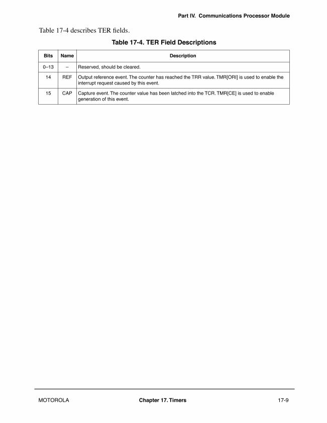
Part IV. Communications Processor Module
Table 17-4 describes TER Þelds.
Table 17-4. TER Field Descriptions
Bits Name Description
0Ð13 Ð Reserved, should be cleared.
14 REF Output reference event. The counter has reached the TRR value. TMR[ORI] is used to enable the interrupt request caused by this event.
15 CAP Capture event. The counter value has been latched into the TCR. TMR[CE] is used to enable generation of this event.
MOTOROLA Chapter 17. Timers 17-9

Part IV. Communications Processor Module
17-10 MPC8260 PowerQUICC II UserÕs Manual MOTOROLA
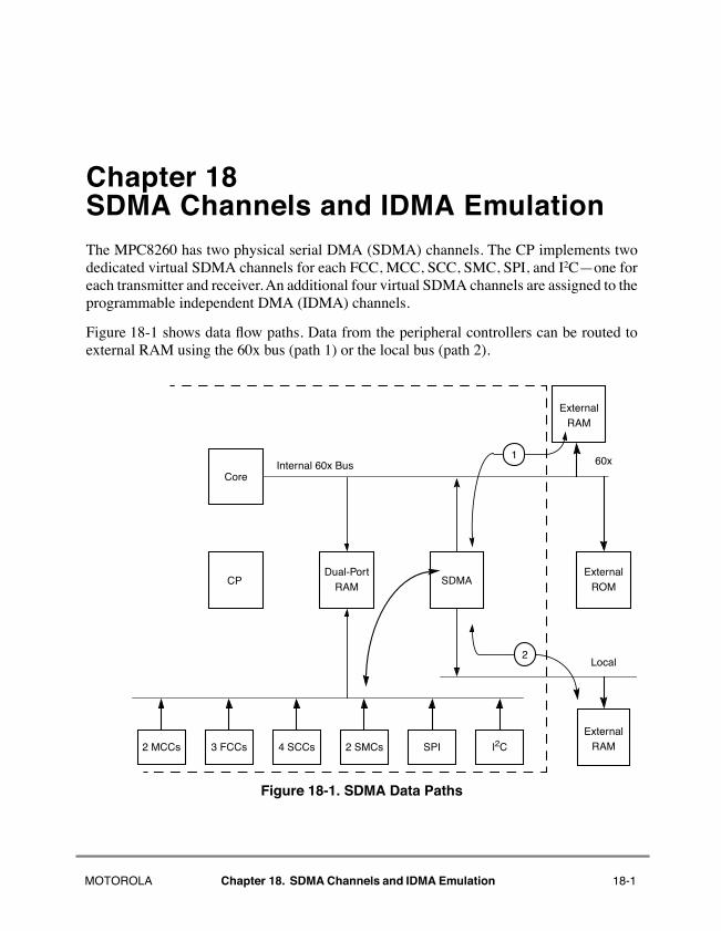
Chapter 18 SDMA Channels and IDMA Emulation180180
The MPC8260 has two physical serial DMA (SDMA) channels. The CP implements twodedicated virtual SDMA channels for each FCC, MCC, SCC, SMC, SPI, and I2CÑone foreach transmitter and receiver. An additional four virtual SDMA channels are assigned to theprogrammable independent DMA (IDMA) channels.
Figure 18-1 shows data ßow paths. Data from the peripheral controllers can be routed toexternal RAM using the 60x bus (path 1) or the local bus (path 2).
Figure 18-1. SDMA Data Paths
ExternalRAM
ExternalROM
Internal 60x BusCore
CP SDMADual-Port
RAM
1
3 FCCs
ExternalRAM
2
60x
Local
2 MCCs 4 SCCs SPI2 SMCs I2C
MOTOROLA Chapter 18. SDMA Channels and IDMA Emulation 18-1
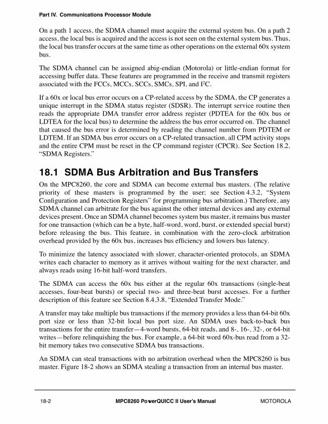
Part IV. Communications Processor Module
On a path 1 access, the SDMA channel must acquire the external system bus. On a path 2access, the local bus is acquired and the access is not seen on the external system bus. Thus,the local bus transfer occurs at the same time as other operations on the external 60x systembus.
The SDMA channel can be assigned abig-endian (Motorola) or little-endian format foraccessing buffer data. These features are programmed in the receive and transmit registersassociated with the FCCs, MCCs, SCCs, SMCs, SPI, and I2C.
If a 60x or local bus error occurs on a CP-related access by the SDMA, the CP generates aunique interrupt in the SDMA status register (SDSR). The interrupt service routine thenreads the appropriate DMA transfer error address register (PDTEA for the 60x bus orLDTEA for the local bus) to determine the address the bus error occurred on. The channelthat caused the bus error is determined by reading the channel number from PDTEM orLDTEM. If an SDMA bus error occurs on a CP-related transaction, all CPM activity stopsand the entire CPM must be reset in the CP command register (CPCR). See Section 18.2,ÒSDMA Registers.Ó
18.1 SDMA Bus Arbitration and Bus TransfersOn the MPC8260, the core and SDMA can become external bus masters. (The relativepriority of these masters is programmed by the user; see Section 4.3.2, ÒSystemConÞguration and Protection RegistersÓ for programming bus arbitration.) Therefore, anySDMA channel can arbitrate for the bus against the other internal devices and any externaldevices present. Once an SDMA channel becomes system bus master, it remains bus masterfor one transaction (which can be a byte, half-word, word, burst, or extended special burst)before releasing the bus. This feature, in combination with the zero-clock arbitrationoverhead provided by the 60x bus, increases bus efÞciency and lowers bus latency.
To minimize the latency associated with slower, character-oriented protocols, an SDMAwrites each character to memory as it arrives without waiting for the next character, andalways reads using 16-bit half-word transfers.
The SDMA can access the 60x bus either at the regular 60x transactions (single-beataccesses, four-beat bursts) or special two- and three-beat burst accesses. For a furtherdescription of this feature see Section 8.4.3.8, ÒExtended Transfer Mode.Ó
A transfer may take multiple bus transactions if the memory provides a less than 64-bit 60xport size or less than 32-bit local bus port size. An SDMA uses back-to-back bustransactions for the entire transferÑ4-word bursts, 64-bit reads, and 8-, 16-, 32-, or 64-bitwritesÑbefore relinquishing the bus. For example, a 64-bit word 60x-bus read from a 32-bit memory takes two consecutive SDMA bus transactions.
An SDMA can steal transactions with no arbitration overhead when the MPC8260 is busmaster. Figure 18-2 shows an SDMA stealing a transaction from an internal bus master.
18-2 MPC8260 PowerQUICC II UserÕs Manual MOTOROLA
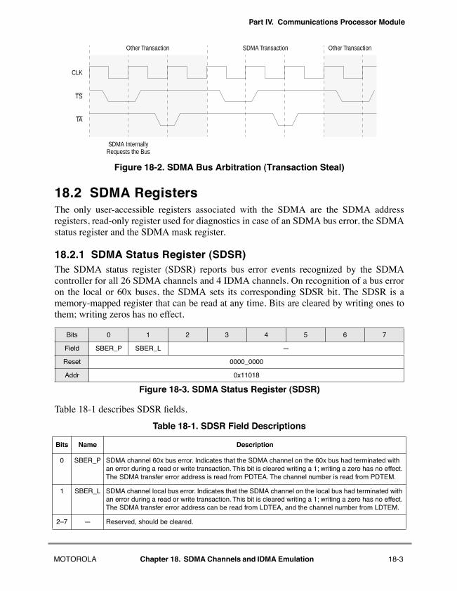
Part IV. Communications Processor Module
Figure 18-2. SDMA Bus Arbitration (Transaction Steal)
18.2 SDMA RegistersThe only user-accessible registers associated with the SDMA are the SDMA addressregisters, read-only register used for diagnostics in case of an SDMA bus error, the SDMAstatus register and the SDMA mask register.
18.2.1 SDMA Status Register (SDSR)The SDMA status register (SDSR) reports bus error events recognized by the SDMAcontroller for all 26 SDMA channels and 4 IDMA channels. On recognition of a bus erroron the local or 60x buses, the SDMA sets its corresponding SDSR bit. The SDSR is amemory-mapped register that can be read at any time. Bits are cleared by writing ones tothem; writing zeros has no effect.
Table 18-1 describes SDSR Þelds.
Bits 0 1 2 3 4 5 6 7
Field SBER_P SBER_L Ñ
Reset 0000_0000
Addr 0x11018
Figure 18-3. SDMA Status Register (SDSR)
Table 18-1. SDSR Field Descriptions
Bits Name Description
0 SBER_P SDMA channel 60x bus error. Indicates that the SDMA channel on the 60x bus had terminated with an error during a read or write transaction. This bit is cleared writing a 1; writing a zero has no effect. The SDMA transfer error address is read from PDTEA. The channel number is read from PDTEM.
1 SBER_L SDMA channel local bus error. Indicates that the SDMA channel on the local bus had terminated with an error during a read or write transaction. This bit is cleared writing a 1; writing a zero has no effect. The SDMA transfer error address can be read from LDTEA, and the channel number from LDTEM.
2Ð7 Ñ Reserved, should be cleared.
CLK
TS
TA
SDMA InternallyRequests the Bus
Other Transaction SDMA Transaction Other Transaction
MOTOROLA Chapter 18. SDMA Channels and IDMA Emulation 18-3
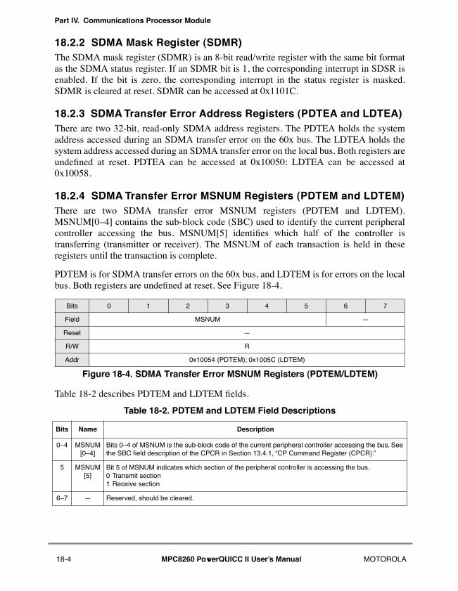
Part IV. Communications Processor Module
18.2.2 SDMA Mask Register (SDMR)The SDMA mask register (SDMR) is an 8-bit read/write register with the same bit formatas the SDMA status register. If an SDMR bit is 1, the corresponding interrupt in SDSR isenabled. If the bit is zero, the corresponding interrupt in the status register is masked.SDMR is cleared at reset. SDMR can be accessed at 0x1101C.
18.2.3 SDMA Transfer Error Address Registers (PDTEA and LDTEA) There are two 32-bit, read-only SDMA address registers. The PDTEA holds the systemaddress accessed during an SDMA transfer error on the 60x bus. The LDTEA holds thesystem address accessed during an SDMA transfer error on the local bus. Both registers areundeÞned at reset. PDTEA can be accessed at 0x10050; LDTEA can be accessed at0x10058.
18.2.4 SDMA Transfer Error MSNUM Registers (PDTEM and LDTEM)There are two SDMA transfer error MSNUM registers (PDTEM and LDTEM).MSNUM[0Ð4] contains the sub-block code (SBC) used to identify the current peripheralcontroller accessing the bus. MSNUM[5] identiÞes which half of the controller istransferring (transmitter or receiver). The MSNUM of each transaction is held in theseregisters until the transaction is complete.
PDTEM is for SDMA transfer errors on the 60x bus, and LDTEM is for errors on the localbus. Both registers are undeÞned at reset. See Figure 18-4.
Table 18-2 describes PDTEM and LDTEM Þelds.
Bits 0 1 2 3 4 5 6 7
Field MSNUM Ñ
Reset Ñ
R/W R
Addr 0x10054 (PDTEM); 0x1005C (LDTEM)
Figure 18-4. SDMA Transfer Error MSNUM Registers (PDTEM/LDTEM)
Table 18-2. PDTEM and LDTEM Field Descriptions
Bits Name Description
0Ð4 MSNUM[0Ð4]
Bits 0Ð4 of MSNUM is the sub-block code of the current peripheral controller accessing the bus. See the SBC Þeld description of the CPCR in Section 13.4.1, ÒCP Command Register (CPCR).Ó
5 MSNUM[5]
Bit 5 of MSNUM indicates which section of the peripheral controller is accessing the bus.0 Transmit section1 Receive section
6Ð7 Ñ Reserved, should be cleared.
18-4 MPC8260 PowerQUICC II UserÕs Manual MOTOROLA
Part IV. Communications Processor Module
18.3 IDMA EmulationThe CPM can be conÞgured to provide general-purpose DMA functionality through theSDMA channel. Four general-purpose independent DMA (IDMA) channels are supported.In this special emulation mode, the user can specify any memory-to-memory orperipheral-to/from-memory transfers as if using dedicated DMA hardware.
The general-purpose IDMA channels can operate in different user-programmable datatransfer modes. The IDMA can transfer data between any combination of memory and I/O.In addition, data may be transferred in either byte, half-word, word, double-word or burstquantities and the source and destination addresses may be odd or even. The most efÞcientpacking algorithms are used in the IDMA transfers. The single-address mode (ßy-by mode)gives the highest performance, allowing data to be transferred between memory and aperipheral in a single bus transaction. The chip-select and wait-state generation logic on theMPC8260 can be used with the IDMA.
The bus bandwidth occupied by the IDMA can be programmed in the IDMA parameterRAM to achieve maximum system performance.
The IDMA supports two buffer handling modesÑauto buffer and buffer chaining. The autobuffer mode allows blocks of data to be repeatedly moved from one location to anotherwithout user intervention. The buffer chaining mode allows a chain of blocks to be moved.The user speciÞes the data movement using BD tables like those used by other peripheralcontrollers. The BD tables reside in the dual-port RAM.
Each IDMA has three signals (DREQx, DACKx and DONEx) for peripheral handshaking.
18.4 IDMA FeaturesThe main IDMA features are as follows:
¥ Four independent, fully programmable DMA channels¥ Dual- or single-address transfers with 32-bit address and 64-bit data capability¥ Memory-to-memory, memory-to-peripheral, and peripheral-to-memory modes¥ 4-Gbyte maximum block length for each buffer¥ 32-bit address pointers that can be optionally incremented¥ Two buffer handling modesÑauto buffer and buffer chaining¥ Interrupts are optionally generated for BD transfer completion, external DONE
assertion, and STOP_IDMA command completion.¥ Any channel is independently conÞgurable for data transfer from any 60x, local bus
source to any 60x, local bus destination¥ Programmable byte-order conversion is supported independently for each DMA
channel¥ Supports programmable 60x-bus bandwidth usage for system performance
optimization
MOTOROLA Chapter 18. SDMA Channels and IDMA Emulation 18-5
Part IV. Communications Processor Module
Peripheral to/from memory features include the following:
¥ External DREQ, DACK, and DONE signals for each channel simpliÞes the peripheral interface for memory-to/from-peripheral transfers
¥ Supports 1-, 2-, 4-, and 8-byte peripheral port sizes¥ Supports standard 60x burst accesses (four consecutive 64-bit data phases) to/from
peripherals
18.5 IDMA TransfersThe IDMA channel transfers data from a source to a destination using an intermediatetransfer buffer (of programmable size) in the dual-port RAM. An efÞcient data-packingalgorithm bursts data through the IDMA transfer buffer to minimize the bus cycles neededfor the transfer. In single-address peripheral transfers, however, data is transferred directlybetween memory and a peripheral device without using the IDMA transfer buffer.
Unaligned data is transferred in single accesses until alignment is achieved. Then, bursttransactions are used (if allowed by the user) to transfer the bulk of the data buffer. Singleaccesses are used again for any remaining non-burstable data at the end of the transfer.
18.5.1 Memory-to-Memory TransfersFor memory-to-memory transfers, the IDMA Þrst Þlls the IDMA transfer buffer in the dual-port RAM by initiating read accesses on the source bus. It then empties the data from theinternal transfer buffer to the destination bus by initiating write accesses. The transfer sizesfor the source and destination buses are programmed in the IDMA parameter RAM.
For the DMA to generate bursts on the 60x bus, the address boundaries of each bursttransfer must be 32-byte aligned. If the transfer does not start on a burst boundary, theIDMA controller transfers the end-of-burst (EOB) data (1Ð31 bytes) in non-bursttransactions on the source bus and on the destination bus until reaching the next boundary.When alignment is achieved, subsequent data is bursted until the remainder of the data inthe buffer is less than a burst size (32 bytes). The remaining data is transferred using non-burst transactions.
Data transfers use the parameters described in Table 18-3.
18-6 MPC8260 PowerQUICC II UserÕs Manual MOTOROLA
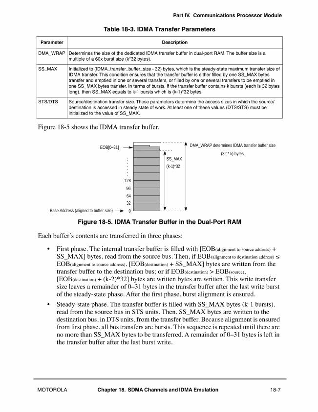
Part IV. Communications Processor Module
Figure 18-5 shows the IDMA transfer buffer.
Figure 18-5. IDMA Transfer Buffer in the Dual-Port RAM
Each bufferÕs contents are transferred in three phases:
¥ First phase. The internal transfer buffer is Þlled with [EOB(alignment to source address) + SS_MAX] bytes, read from the source bus. Then, if EOB(alignment to destination address) £ EOB(alignment to source address), [EOB(destination) + SS_MAX] bytes are written from the transfer buffer to the destination bus; or if EOB(destination) > EOB(source), [EOB(destination) + (k-2)*32] bytes are written bytes are written. This write transfer size leaves a remainder of 0Ð31 bytes in the transfer buffer after the last write burst of the steady-state phase. After the Þrst phase, burst alignment is ensured.
¥ Steady-state phase. The transfer buffer is Þlled with SS_MAX bytes (k-1 bursts), read from the source bus in STS units. Then, SS_MAX bytes are written to the destination bus, in DTS units, from the transfer buffer. Because alignment is ensured from Þrst phase, all bus transfers are bursts. This sequence is repeated until there are no more than SS_MAX bytes to be transferred. A remainder of 0Ð31 bytes is left in the transfer buffer after the last burst write.
Table 18-3. IDMA Transfer Parameters
Parameter Description
DMA_WRAP Determines the size of the dedicated IDMA transfer buffer in dual-port RAM. The buffer size is a multiple of a 60x burst size (k*32 bytes).
SS_MAX Initialized to (IDMA_transfer_buffer_size - 32) bytes, which is the steady-state maximum transfer size of IDMA transfer. This condition ensures that the transfer buffer is either Þlled by one SS_MAX bytes transfer and emptied in one or several transfers, or Þlled by one or several transfers to be emptied in one SS_MAX bytes transfer. In terms of bursts, if the transfer buffer contains k bursts (each is 32 bytes long), then SS_MAX equals to k-1 bursts which is (k-1)*32 bytes.
STS/DTS Source/destination transfer size. These parameters determine the access sizes in which the source/destination is accessed in steady state of work. At least one of these values (DTS/STS) must be initialized to the value of SS_MAX.
SS_MAX
DMA_WRAP determines IDMA transfer buffer sizeEOB[0–31]
32
64
96
0
128
(k-1)*32
(32 * k) bytes
Base Address (aligned to buffer size)
MOTOROLA Chapter 18. SDMA Channels and IDMA Emulation 18-7
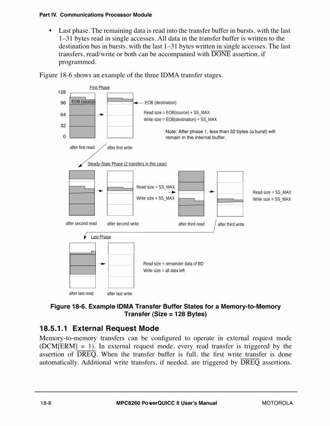
Part IV. Communications Processor Module
¥ Last phase. The remaining data is read into the transfer buffer in bursts, with the last 1Ð31 bytes read in single accesses. All data in the transfer buffer is written to the destination bus in bursts, with the last 1Ð31 bytes written in single accesses. The last transfers, read/write or both can be accompanied with DONE assertion, if programmed.
Figure 18-6 shows an example of the three IDMA transfer stages.
Figure 18-6. Example IDMA Transfer Buffer States for a Memory-to-Memory Transfer (Size = 128 Bytes)
18.5.1.1 External Request ModeMemory-to-memory transfers can be conÞgured to operate in external request mode(DCM[ERM] = 1). In external request mode, every read transfer is triggered by theassertion of DREQ. When the transfer buffer is full, the Þrst write transfer is doneautomatically. Additional write transfers, if needed, are triggered by DREQ assertions.
First Phase
after first read after first write
after second read after second write after third read after third write
Steady-State Phase (2 transfers in this case)
Last Phase
after last read after last write
Read size = EOB(source) + SS_MAXWrite size = EOB(destination) + SS_MAX
Read size = SS_MAXWrite size = SS_MAX
Read size = remainder data of BDWrite size = all data left
EOB (source) EOB (destination)
0
32
64
96
128
Read size = SS_MAX
Write size = SS_MAX
Note: After phase 1, less than 32 bytes (a burst) willremain in the internal buffer.
18-8 MPC8260 PowerQUICC II UserÕs Manual MOTOROLA
Part IV. Communications Processor Module
Because at least one of the transfer sizes (STS or DTS) equals SS_MAX, every DREQassertion causes one transfer to the smaller (in STS/DTS terms) bus. If STS = DTS,asserting DREQ triggers one read transfer automatically followed by one write transfer.
NOTEExternal request mode does not support external DONEsignaling from a device and DACK signaling from an IDMAchannel.
18.5.1.2 Normal ModeWhen external request mode is not selected (DCM[ERM] = 0), the IDMA channel operatesautomatically, ignoring DREQ.
18.5.2 Memory to/from Peripheral TransfersWorking with peripheral devices requires the external signals DONE, DREQ, DACK tocontrol the data transfer using the following rules:
¥ The peripheral sets a request for data to be read-from/write-to by asserting DREQ as conÞgured, falling or rising edge sensitive.
¥ The peripheral transfers/samples the data when DACK is asserted.
¥ The peripheral asserts DONE to stop the current transfer.
¥ The peripheral terminates the current transfer when DONE is asserted, combined with DACK, by the IDMA.
Peripherals are usually accessed with Þxed port-size transfers. The transfer sizes (STS/DTS) related to the peripheral must be programmed to its port size; thus, every access to aperipheral yields a single bus transaction. The maximum peripheral port size is (bus_width- 8) bytes and also should evenly divide the buffer length, BD[Data Length].
A peripheral can also be conÞgured to accept a burst per DREQ assertion. In this case, thetransfer size parameter should be initialized to 32, and the accesses are made in bursts. SeeTable 18-8.
A peripheral can be accessed at a Þxed address location or at incremental addresses. SettingDCM[SINC, DINC] in the DMA channel mode register causes the address to beincremented before the next transfer; see Section 18.8.2.1, ÒDMA Channel Mode (DCM).ÓThis allows the IDMA to access a FIFO buffer the same way it does peripherals.
DCM[S/D] determines whether the peripheral is the source or destination.
MOTOROLA Chapter 18. SDMA Channels and IDMA Emulation 18-9
Part IV. Communications Processor Module
Data can be transferred between a peripheral and memory in single- or dual-addressaccesses:
¥ For dual-address accesses, the data is read from the source, temporarily stored in the IDMA transfer buffer in the dual-port RAM, and then written to the destination.
¥ For single-address accesses (ßy-by mode), the data is transferred directly between memory and the peripheral. Memory responds to the address phase, while the peripheral ignores it and responds to DACK assertions.
Any IDMA access to a peripheral uses the highest arbitration priority allowed for the DMA,providing faster bus access by bypassing other pending DMA requests.
18.5.2.1 Dual-Address TransfersThe following sections discuss various dual-address transfers.
18.5.2.1.1 Peripheral to MemoryDual-address peripheral-to-memory data transfers are similar to memory-to-memorytransfers using the three-phase algorithm; see Section 18.5.1, ÒMemory-to-MemoryTransfers.Ó When a peripheral asserts DREQ, data is loaded from the peripheral in port-sizeunits to the internal transfer buffer. When the transfer buffer reaches the steady-state level,it is automatically written to the memory destination in one transfer. The source transfersize (STS) is initialized to the peripheral port size, and the destination transfer size (DTS)is initialized to SS_MAX.
External requests must be enabled (DCM[ERM] = 1) for dual-address peripheral-to-memory transfers. If DONE is asserted externally by the peripheral or if a STOP_IDMA
command is issued, the current transfer stops. All data in the internal transfer buffer iswritten to memory in one transfer before its BD is closed, and the IDSR[EDN] orIDSR[SC] event bits are set; see Section 18.8.4, ÒIDMA Event Register (IDSR) and MaskRegister (IDMR).Ó
When the peripheral controls a transfer of unknown length, initialize a large enough bufferso that the peripheral will most likely assert DONE before overßowing the buffer. WhenDONE is asserted, the BD is closed and interrupts are generated (if enabled). The nextDREQ assertion opens the next BD if DCM[DT] is set; see Section 18.8.2.1, ÒDMAChannel Mode (DCM).Ó
18.5.2.1.2 Memory to PeripheralDual-address memory-to-peripheral data transfers are similar to memory-to-memorytransfers using the three-phase algorithm; see Section 18.5.1, ÒMemory-to-MemoryTransfers.Ó STS is initialized to SS_MAX and DTS is initialized to the peripheral port size.The Þrst DREQ peripheral assertion triggers a read of SS_MAX (or more in the Þrst phase)bytes from the memory into the internal transfer buffer, automatically followed by a writeof DTS bytes to the peripheral. Subsequent DREQ assertions trigger writes to the
18-10 MPC8260 PowerQUICC II UserÕs Manual MOTOROLA
Part IV. Communications Processor Module
peripheral. When the transfer buffer has fewer than DTS bytes left, the next DREQassertion triggers a read of SS_MAX bytes from memory, automatically followed by awrite to the peripheral, and the sequence begins again.
External requests must be enabled (DCM[ERM] = 1) for dual-address peripheral-to-memory transfers. If DONE is asserted externally by the peripheral or if a STOP_IDMA
command is issued, the current transfer is stopped, its BD is closed, and the IDSR[EDN]or IDSR[SC] event bits are set; see Section 18.8.4, ÒIDMA Event Register (IDSR) andMask Register (IDMR).Ó
18.5.2.2 Single Address (Fly-By) TransfersWhen DCM[FB] = 1, both peripheral-to-memory and memory-to-peripheral transfersoccur in ßy-by mode; see Section 18.8.2.1, ÒDMA Channel Mode (DCM).Ó In fly-by mode,an internal transfer buffer is not needed because the data is transferred directly betweenmemory and the peripheral. Also, parameters related to the dual-port RAM bus are notrelevant in ßy-by mode. Each DREQ assertion triggers a transfer the size of the peripheralport. All transfers are made in single memory accesses accompanied by DACK assertion.When DONE is asserted externally or a STOP_IDMA command is issued, the current transferis stopped, its BD is closed, and the IDSR[EDN] or IDSR[SC] event bits are set; seeSection 18.8.4, ÒIDMA Event Register (IDSR) and Mask Register (IDMR).Ó
In ßy-by mode, a peripheral can be conÞgured to handle a burst per DREQ assertion if STSis programmed to 32. The Þrst phase of the transfer aligns the data to the burst boundary sothat subsequent accesses can be performed in bursts.
18.5.2.2.1 Peripheral-to-Memory Fly-By TransfersDuring peripheral-to-memory ßy-by transfers, the IDMA controller writes to memorywhile simultaneously asserting DACK. The constant assertion of DACK enables thecontroller to write to memory as soon as the peripheral outputs data to the bus. Thus, datais transferred from a peripheral to memory in one data phase instead of two, increasingthroughput.
For proper operation, STS must equal the peripheral port size.
18.5.2.2.2 Memory-to-Peripheral Fly-By TransfersDuring memory-to-peripheral ßy-by transfers, the IDMA controller reads from memorywhile simultaneously asserting DACK.
The constant assertion of DACK enables the controller to read from memory as soon as theperipheral samples the data bus. Thus, data is transferred from memory to a peripheral inone data phase instead of two, increasing throughput.
For proper operation, DTS must equal the peripheral port size.
MOTOROLA Chapter 18. SDMA Channels and IDMA Emulation 18-11
Part IV. Communications Processor Module
18.5.3 Controlling 60x Bus BandwidthSTS, DTS, and SS_MAX can be used to control the 60x bus bandwidth occupied by theIDMA channel. In every mode except ßy-by mode, at least one transfer size parameter(STS/DTS) must be initialized to the SS_MAX value. For memory-to-memory transfers,the other transfer size parameter can be initialized to a smaller value used to control the 60xbus bandwidth. For example, if the transfer size is N*32 bytes, each time the DMAcontroller wins arbitration, it transfers N bursts before releasing the bus. When SS_MAXbytes have been transferred, the controller reverts to single transactions (double-word,word, half-word, or byte).
Memory-to-memory transfer sizes must evenly divide into SS_MAX and also be a multipleof 32 (for bursting); see Table 18-7.
The size of the IDMA transfer buffer in the dual-port RAM should be determined by thelargest transfer (usually SS_MAX + 32 bytes) needed by one of the buses, while the othertransfer size can be programmed to control the bandwidth of the other bus.
Summarizing the above, a larger DMA transfer size provides for greater microcodeefÞciency and lower DMA bus latency, because the DMA controller does not release the60x bus until the transfer is completed. If the DMA priority on the 60x bus is high, however,other 60x masters may experience a high bus latency. Conversely, if the transfer size issmall, the DMA requests the 60x bus more often, DMA latency increases and microcodeefÞciency decreases.
The IDMA transfer size parameters give high ßexibility, but it is recommended to checkoverall system performance with different IDMA parameter settings for maximumthroughput.
Note that the memory priority parameter DCM[LP] should be considered when dealingwith bus bandwidth usage.
18.6 IDMA PrioritiesEach IDMA channel can be programmed to have a higher or lower priority relative to theserial controllers or to have the lowest overall priority when requesting service from the CP.The IDMA priorities are programmed in RCCR[DRxQP]; see Section 13.3.6, ÒRISCController ConÞguration Register (RCCR).Ó Take care to avoid overrun or underrun errorsin the serial controllers when selecting high priorities for IDMA.
Additional priority over all serial controllers can be selected by setting DCM[LP]; seeSection 18.8.2.1, ÒDMA Channel Mode (DCM).Ó
18.7 IDMA Interface SignalsEach IDMA has three dedicated handshake control signals for transfers involving anexternal peripheral device: DMA request (DREQ[1Ð4]), DMA acknowledge (DACK[1Ð4])
18-12 MPC8260 PowerQUICC II UserÕs Manual MOTOROLA
Part IV. Communications Processor Module
and DMA done (DONE[1Ð4]). DREQx may also be used to control the transfer pace ofmemory-to-memory transfers.
¥ DREQx is the external DMA request signal.
¥ DACKx is the DMA acknowledge.
¥ DONEx marks the end of an IDMA transfer.
The IDMA signals are multiplexed with other internal controller signals at the parallel I/Oports. To enable the IDMA signals, the corresponding bits in the parallel I/O registersshould be set. See Chapter 35, ÒParallel I/O Ports.Ó
18.7.1 DREQx and DACKx When the peripheral requires IDMA service, it asserts DREQx and the MPC8260 beginsthe IDMA process. When the IDMA service is in progress, DACKx is asserted duringaccesses to the peripheral. A peripheral must validate the transfer by asserting TA or signalan error by asserting TEA.
DREQx may be conÞgured as either edge- or level-sensitive by programming theRCCR[DRxM]. When DREQx is conÞgured as edge-sensitive, RCCR[EDMx] controlswhether the request is generated on the rising or falling edge; see Section 13.3.6, ÒRISCController ConÞguration Register (RCCR).Ó
DREQx is sampled at each rising edge of the clock to determine when a valid request isasserted by the device.
18.7.1.1 Level-Sensitive ModeFor external devices requiring very high data transfer rates, level-sensitive mode allows theIDMA to use a maximum bandwidth to service the device. The device requests service byasserting DREQx and leaving it asserted as long as it needs service. This mode is selectedby setting the corresponding RCCR[DRxM].
The IDMA asserts DACK each time it issues a bus transaction to either read or write theperipheral. The peripheral must use TA and TEA for data validation. DACK is theacknowledgment of the original burst request given on DREQx. DREQx should be negatedduring the DACK active period to ensure that no further transactions are performed.
18.7.1.2 Edge-Sensitive ModeFor external devices that generate a pulsed signal for each operand to be transferred, edge-sensitive mode should be used. In edge-sensitive mode, the IDMA controller moves oneoperand for each falling/rising (as conÞgured by RCCR[EDMx]) edge of DREQx. Thismode is selected by clearing the corresponding RCCR[DRxM] and programming thecorresponding RCCR[EDMx] to the proper edge.
When the IDMA controller detects a valid edge on DREQx, a request becomes pending andremains pending until it is serviced by the IDMA. Subsequent changes on DREQx are
MOTOROLA Chapter 18. SDMA Channels and IDMA Emulation 18-13
Part IV. Communications Processor Module
ignored until the request begins to be serviced. The servicing of the request results in oneoperand being transferred. Each time the IDMA issues a bus transaction to either read orwrite the device, the IDMA asserts DACK. The device must use TA and TEA for datavalidation. Thus, DACK is the acknowledgment of the original transaction request given onDREQx.
18.7.2 DONEx This bidirectional open-drain signal is used to indicate the last IDMA transfer. DONE canbe an output of the IDMA in the source or destination bus transaction if the transfer countis exhausted. This function is controlled by BD[SDN, DDN].
DONE can also operate as an input. When operating in external request modes, DONE maybe used as an input to the IDMA controller to indicate that the device being servicedrequires no more transfers. In that case, the transfer is terminated, the current BD is closed,and an interrupt is generated (if enabled).
NOTE
DONE is ignored if it is asserted externally during internalrequest mode (DCM[ERM] = 0).
DONE must not be asserted externally during memory-to-memory transfers if external request mode is enabled(DCM[ERM] = 1).
18.8 IDMA OperationEvery IDMA operation involves the following stepsÑIDMA channel initialization, datatransfer, and block termination.
¥ During initialization, the core initializes the IDMA_BASE register in the internal parameter RAM to point to the IDMA-speciÞc table in RAM. This table contains control information for the IDMA operation. In addition the core initializes the parallel I/O registers to enable IDMA external signals, if needed, and other registers related to the channel priority and operation modes; see Section 18.11, ÒProgramming the Parallel I/O Registers.Ó The core initiates the IDMA BDs to point to the data for the transfer and/or a free space for data to be transferred to, and starts the transfer by issuing the START_IDMA command.
¥ During data transfer, the IDMA accepts requests for data transfers and provides addressing and bus control for the transfers.
¥ Termination occurs when the IDMA operation completes or the peripheral asserts DONE externally. The core can initiate termination by using the STOP_IDMA command. The IDMA can interrupt the core if interrupts are enabled to signal for operation termination and other events related to the data transfer.
The IDMA uses a data structure, which, as with serial controller BDs, allows ßexible data
18-14 MPC8260 PowerQUICC II UserÕs Manual MOTOROLA
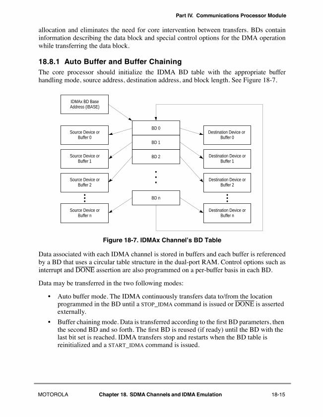
Part IV. Communications Processor Module
allocation and eliminates the need for core intervention between transfers. BDs containinformation describing the data block and special control options for the DMA operationwhile transferring the data block.
18.8.1 Auto Buffer and Buffer Chaining The core processor should initialize the IDMA BD table with the appropriate bufferhandling mode, source address, destination address, and block length. See Figure 18-7.
Figure 18-7. IDMAx ChannelÕs BD Table
Data associated with each IDMA channel is stored in buffers and each buffer is referencedby a BD that uses a circular table structure in the dual-port RAM. Control options such asinterrupt and DONE assertion are also programmed on a per-buffer basis in each BD.
Data may be transferred in the two following modes:
¥ Auto buffer mode. The IDMA continuously transfers data to/from the location programmed in the BD until a STOP_IDMA command is issued or DONE is asserted externally.
¥ Buffer chaining mode. Data is transferred according to the Þrst BD parameters, then the second BD and so forth. The Þrst BD is reused (if ready) until the BD with the last bit set is reached. IDMA transfers stop and restarts when the BD table is reinitialized and a START_IDMA command is issued.
IDMAx BD BaseAddress (IBASE)
Source Device orBuffer 0
Source Device orBuffer 1
Source Device orBuffer 2
Source Device orBuffer n
BD 0Destination Device or
Buffer 0BD 1
BD 2
BD n
Destination Device orBuffer 1
Destination Device orBuffer 2
Destination Device orBuffer n
•••
••••••
MOTOROLA Chapter 18. SDMA Channels and IDMA Emulation 18-15
Part IV. Communications Processor Module
18.8.2 IDMAx Parameter RAMWhen an IDMAx channel is conÞgured to auto buffer or buffer chaining mode, theMPC8260 uses the IDMAx parameters listed in the Table 18-4. Parameters should bemodiÞed only while the channel is disabled, that is, before the Þrst START_IDMA commandor when the event registerÕs stop-completed bit (IDSR[SC]) is set following a STOP_IDMA
command.
Each IDMAx channel parameter table can be placed at any 64-byte aligned address in thedual-port RAMÕs general-purpose area (banks 1Ð8). The CP accesses each IDMAx channelparameter table using a user-programmed pointer (IDMAx_BASE) located in theparameter RAM; see Section 13.5.2, ÒParameter RAM.Ó For example, if the IDMA1channel parameter table is to be placed at address offset 0x2000 in the dual-port RAM,write 0x2000 to IDMA1_BASE.
Table 18-4. IDMAx Parameter RAM
Offset 1 Name Width Description
0x00 IBASE Hword IDMA BD table base address. DeÞnes the starting location in the dual-port RAM for the set of IDMA BDs. It is an offset from the beginning of the dual-port RAM. The user must initialize IBASE before enabling the IDMA channel and should not overlap BD tables of two enabled serial controllers or IDMA channels or erratic operation results. The IBASE value should be 16-bit aligned.
0x02 DCM Hword DMA channel mode. See Section 18.8.2.1, ÒDMA Channel Mode (DCM).Ó
0x04 IBDPTR Hword IDMA BD pointer. Points to the current BD during transfer processing. Points to the next BD to be processed when an idle channel is restarted. Initialize to IBASE before the Þrst START_IDMA command. If BD[W] = 1, the CP initializes IBPTR to IBASE When the end of an IDMA BD table is reached. After a STOP_IDMA command is issued, IBDPTR points to the next BD to be processed. It can be modiÞed after SC interrupt is set and before a START_IDMA command is reissued.
0x06 DPR_BUF Hword IDMA transfer buffer base address. The base address should be aligned according to the buffer size determined by DCM[DMA_WRAP]. The transfer buffer size should be consistent with DCM[DMA_WRAP]; that is, DPR_BUF = (64 X 2DMA_WRAP) - 32. See Section 18.8.2.1, ÒDMA Channel Mode (DCM).Ó
0x08 BUF_INV Hword Internal buffer inventory. Indicates the quantity of data inside the internal buffer.
0x0A SS_MAX Hword Steady-state maximum transfer size in bytes. User-deÞned parameter to increase microcode efÞciency. Initialize to internal_buffer_size - 32, that is, SS_MAX = (64 X 2DMA_WRAP) - 32. If possible, SS_MAX is used as the transfer size on transfers to/from memory in memory-to-peripheral mode or in peripheral-to-memory mode. For memory-to-memory mode, SS_MAX is used as the transfer size for at least one of the devices. SS_MAX should be consistent with STS, DTS, and DCM[S/D]. See Table 18-7 and Table 18-8.
0x0C DPR_IN_PTR Hword Write pointer inside the internal buffer.
18-16 MPC8260 PowerQUICC II UserÕs Manual MOTOROLA
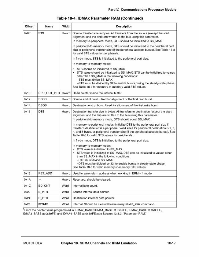
Part IV. Communications Processor Module
0x0E STS Hword Source transfer size in bytes. All transfers from the source (except the start alignment and the end) are written to the bus using this parameter.In memory-to-peripheral mode, STS should be initialized to SS_MAX.
In peripheral-to-memory mode, STS should be initialized to the peripheral port size or peripheral transfer size (if the peripheral accepts bursts). See Table 18-8 for valid STS values for peripherals.
In ßy-by mode, STS is initialized to the peripheral port size.
In memory-to-memory mode:
¥ STS should be initialized to SS_MAX.¥ DTS value should be initialized to SS_MAX. STS can be initialized to values
other than SS_MAX in the following conditions: ÐSTS must divide SS_MAX.ÐSTS must be divided by 32 to enable bursts during the steady-state phase.
See Table 18-7 for memory-to-memory valid STS values.
0x10 DPR_OUT_PTR Hword Read pointer inside the internal buffer.
0x12 SEOB Hword Source end of burst. Used for alignment of the Þrst read burst.
0x14 DEOB Hword Destination end of burst. Used for alignment of the Þrst write burst.
0x16 DTS Hword Destination transfer size in bytes. All transfers to destination (except the start alignment and the tail) are written to the bus using this parameter.In peripheral-to-memory mode, DTS should equal SS_MAX.
In memory-to-peripheral modes, initialize DTS to the peripheral port size if transferÕs destination is a peripheral. Valid sizes for peripheral destination is 1, 2, 4, and 8 bytes, or peripheral transfer size (if the peripheral accepts bursts). See Table 18-8 for valid STS values for peripherals.
In ßy-by mode, DTS is initialized to the peripheral port size.
In memory-to-memory mode:¥ DTS value is initialized to SS_MAX.¥ STS value is initialized to SS_MAX. DTS can be initialized to values other
than SS_MAX in the following conditions: ÐDTS must divide SS_MAX.ÐDTS must be divided by 32, to enable bursts in steady-state phase.
See Table 18-8 for valid memory-to-memory DTS values.
0x18 RET_ADD Hword Used to save return address when working in ERM = 1 mode.
0x1A Ñ Hword Reserved, should be cleared.
0x1C BD_CNT Word Internal byte count.
0x20 S_PTR Word Source internal data pointer.
0x24 D_PTR Word Destination internal data pointer.
0x28 ISTATE Word Internal. Should be cleared before every START_IDMA command.
1From the pointer value programmed in IDMAx_BASE: IDMA1_BASE at 0x87FE, IDMA2_BASE at 0x88FE, IDMA3_BASE at 0x89FE, and IDMA4_BASE at 0x8AFE; see Section 13.5.2, ÒParameter RAM.Ó
Table 18-4. IDMAx Parameter RAM (Continued)
Offset 1 Name Width Description
MOTOROLA Chapter 18. SDMA Channels and IDMA Emulation 18-17
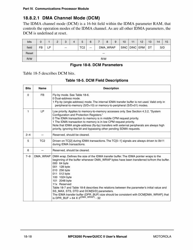
Part IV. Communications Processor Module
18.8.2.1 DMA Channel Mode (DCM)The IDMA channel mode (DCM) is a 16-bit Þeld within the IDMA parameter RAM, thatcontrols the operation modes of the IDMA channel. As are all other IDMA parameters, theDCM is undeÞned at reset.
Table 18-5 describes DCM bits.
bits 0 1 2 3 4 5 6 7 8 9 10 11 12 13 14 15
Þeld FB LP Ñ TC2 Ñ DMA_WRAP SINC DINC ERM DT S/D
Reset Ñ
R/W R/W
Figure 18-8. DCM Parameters
Table 18-5. DCM Field Descriptions
Bits Name Description
0 FB Fly-by mode. See Table 18-6.0 Dual-address mode.1 Fly-by (single-address) mode. The internal IDMA transfer buffer is not used. Valid only in
peripheral-to-memory (S/D=10) or memory-to-peripheral (S/D=01) modes.
1 LP Low priority. Applies to memory-to-memory accesses only. See Section 4.3.2, ÒSystem ConÞguration and Protection Registers.Ó0 The IDMA transaction to memory is in middle CPM request priority.1 The IDMA transaction to memory is in low CPM request priority.Note that IDMA single-address (ßy-by) transfers with external peripherals are always high priority, ignoring this bit and bypassing other pending SDMA requests.
2Ð4 Ñ Reserved, should be cleared.
5 TC2 Driven on TC[2] during IDMA transactions. The TC[0Ð1] signals are always driven to 0b11 during IDMA transactions.
6 Ñ Reserved, should be cleared.
7Ð9 DMA_WRAP DMA wrap. DeÞnes the size of the IDMA transfer buffer. The IDMA pointer wraps to the beginning of the buffer whenever DMA_WRAP bytes have been transferred to/from the buffer.000 64 byte 001 128 byte 010 256 byte 011 512 byte 100 1024 byte 101 2048 byte 11x ReservedTable 18-7 and Table 18-8 describes the relations between the parameterÕs initial value and SS_MAX, STS, DTD and DCM[S/D] parameters. The IDMA transfer buffer (DPR_BUF) size should be consistent with DCM[DMA_WRAP]; that is DPR_BUF = 64 X 2(DMA_WRAP) - 32
18-18 MPC8260 PowerQUICC II UserÕs Manual MOTOROLA
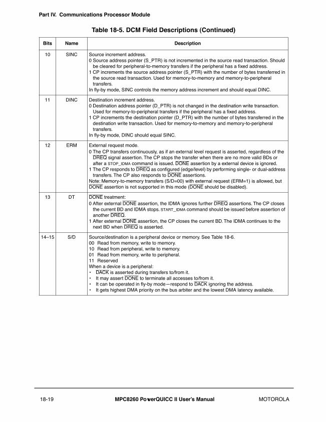
Part IV. Communications Processor Module
10 SINC Source increment address.0 Source address pointer (S_PTR) is not incremented in the source read transaction. Should
be cleared for peripheral-to-memory transfers if the peripheral has a Þxed address. 1 CP increments the source address pointer (S_PTR) with the number of bytes transferred in
the source read transaction. Used for memory-to-memory and memory-to-peripheral transfers.
In ßy-by mode, SINC controls the memory address increment and should equal DINC.
11 DINC Destination increment address.0 Destination address pointer (D_PTR) is not changed in the destination write transaction.
Used for memory-to-peripheral transfers if the peripheral has a Þxed address.1 CP increments the destination pointer (D_PTR) with the number of bytes transferred in the
destination write transaction. Used for memory-to-memory and memory-to-peripheral transfers.
In ßy-by mode, DINC should equal SINC.
12 ERM External request mode.0 The CP transfers continuously, as if an external level request is asserted, regardless of the
DREQ signal assertion. The CP stops the transfer when there are no more valid BDs or after a STOP_IDMA command is issued. DONE assertion by a external device is ignored.
1 The CP responds to DREQ as conÞgured (edge/level) by performing single- or dual-address transfers. The CP also responds to DONE assertions.
Note: Memory-to-memory transfers (S/D=00) with external request (ERM=1) is allowed, but DONE assertion is not supported in this mode (DONE should be disabled).
13 DT DONE treatment:0 After external DONE assertion, the IDMA ignores further DREQ assertions. The CP closes
the current BD and IDMA stops. START_IDMA command should be issued before assertion of another DREQ.
1 After external DONE assertion, the CP closes the current BD. The IDMA continues to the next BD when DREQ is asserted.
14Ð15 S/D Source/destination is a peripheral device or memory. See Table 18-6.00 Read from memory, write to memory.10 Read from peripheral, write to memory.01 Read from memory, write to peripheral.11 ReservedWhen a device is a peripheral: ¥ DACK is asserted during transfers to/from it.¥ It may assert DONE to terminate all accesses to/from it.¥ It can be operated in ßy-by modeÑrespond to DACK ignoring the address.¥ It gets highest DMA priority on the bus arbiter and the lowest DMA latency available.
Table 18-5. DCM Field Descriptions (Continued)
Bits Name Description
18-19 MPC8260 PowerQUICC II UserÕs Manual MOTOROLA
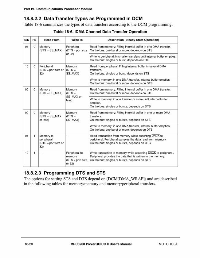
Part IV. Communications Processor Module
18.8.2.2 Data Transfer Types as Programmed in DCMTable 18-6 summarizes the types of data transfers according to the DCM programming.
18.8.2.3 Programming DTS and STSThe options for setting STS and DTS depend on (DCM[DMA_WRAP]) and are describedin the following tables for memory/memory and memory/peripheral transfers.
Table 18-6. IDMA Channel Data Transfer Operation
S/D FB Read From Write To Description (Steady-State Operation)
01 0 Memory(STS = SS_MAX)
Peripheral(DTS = port size or 32)
Read from memory: Filling internal buffer in one DMA transfer.On the bus: one burst or more, depends on STS
Write to peripheral: In smaller transfers until internal buffer empties. On the bus: singles or burst, depends on DTS
10 0 Peripheral(STS = port size or 32)
Memory(DTS = SS_MAX)
Read from peripheral: Filling internal buffer in several DMA transfers.On the bus: singles or burst, depends on STS
Write to memory: in one DMA transfer, internal buffer empties. On the bus: one burst or more, depends on DTS
00 0 Memory(STS = SS_MAX)
Memory(DTS = SS_MAX or less)
Read from memory: Filling internal buffer in one DMA transfer.On the bus: one burst or more, depends on STS
Write to memory: in one transfer or more until internal buffer empties. On the bus: singles or bursts, depends on DTS
00 0 Memory(STS = SS_MAX or less)
Memory(DTS = SS_MAX)
Read from memory: Filling internal buffer in one or more DMA transfers.On the bus: singles or bursts, depends on STS
Write to memory: in one DMA transfer, internal buffer empties. On the bus: one burst or more, depends on DTS
01 1 Memory to peripheral(DTS = port size or 32)
Ñ Read transaction from memory while asserting DACK to peripheral. Peripheral samples the data read from memory.On the bus: singles or bursts, depends on DTS
10 1 Ñ Peripheral to memory(STS = port size or 32)
Write transaction to memory while asserting DACK to peripheral. Peripheral provides the data that is written to the memory.On the bus: singles or bursts, depends on STS
18-20 MPC8260 PowerQUICC II UserÕs Manual MOTOROLA
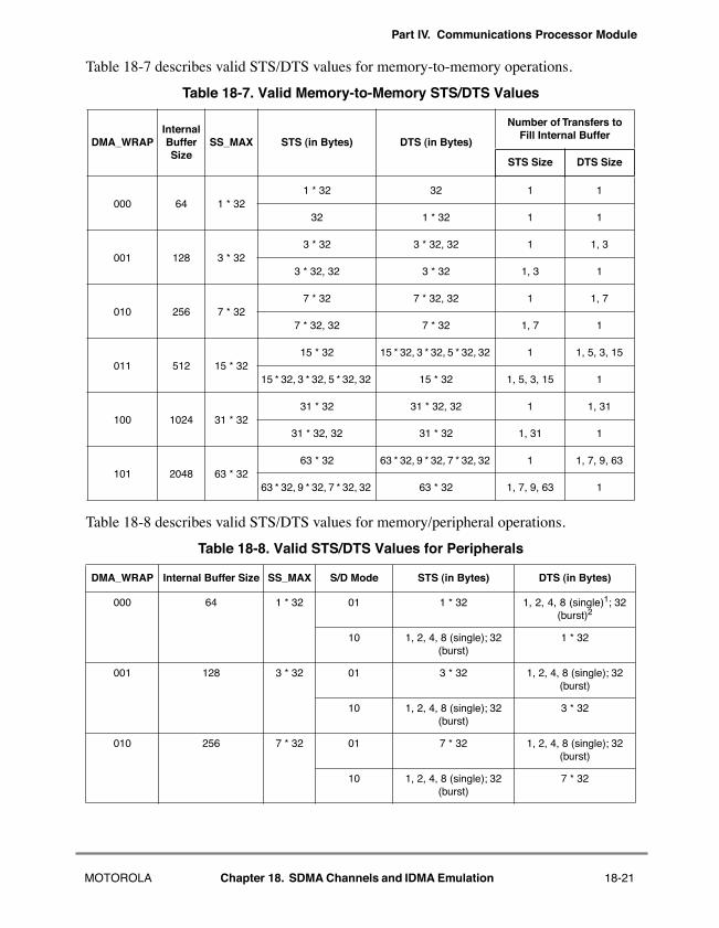
Part IV. Communications Processor Module
Table 18-7 describes valid STS/DTS values for memory-to-memory operations.
Table 18-8 describes valid STS/DTS values for memory/peripheral operations.
Table 18-7. Valid Memory-to-Memory STS/DTS Values
DMA_WRAPInternal Buffer Size
SS_MAX STS (in Bytes) DTS (in Bytes)
Number of Transfers to Fill Internal Buffer
STS Size DTS Size
000 64 1 * 321 * 32 32 1 1
32 1 * 32 1 1
001 128 3 * 323 * 32 3 * 32, 32 1 1, 3
3 * 32, 32 3 * 32 1, 3 1
010 256 7 * 327 * 32 7 * 32, 32 1 1, 7
7 * 32, 32 7 * 32 1, 7 1
011 512 15 * 3215 * 32 15 * 32, 3 * 32, 5 * 32, 32 1 1, 5, 3, 15
15 * 32, 3 * 32, 5 * 32, 32 15 * 32 1, 5, 3, 15 1
100 1024 31 * 3231 * 32 31 * 32, 32 1 1, 31
31 * 32, 32 31 * 32 1, 31 1
101 2048 63 * 3263 * 32 63 * 32, 9 * 32, 7 * 32, 32 1 1, 7, 9, 63
63 * 32, 9 * 32, 7 * 32, 32 63 * 32 1, 7, 9, 63 1
Table 18-8. Valid STS/DTS Values for Peripherals
DMA_WRAP Internal Buffer Size SS_MAX S/D Mode STS (in Bytes) DTS (in Bytes)
000 64 1 * 32 01 1 * 32 1, 2, 4, 8 (single)1; 32 (burst)2
10 1, 2, 4, 8 (single); 32 (burst)
1 * 32
001 128 3 * 32 01 3 * 32 1, 2, 4, 8 (single); 32 (burst)
10 1, 2, 4, 8 (single); 32 (burst)
3 * 32
010 256 7 * 32 01 7 * 32 1, 2, 4, 8 (single); 32 (burst)
10 1, 2, 4, 8 (single); 32 (burst)
7 * 32
MOTOROLA Chapter 18. SDMA Channels and IDMA Emulation 18-21
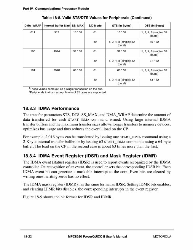
Part IV. Communications Processor Module
18.8.3 IDMA PerformanceThe transfer parameters STS, DTS, SS_MAX, and DMA_WRAP determine the amount ofdata transferred for each START_IDMA command issued. Using large internal IDMAtransfer buffers and the maximum transfer sizes allows longer transfers to memory devices,optimizes bus usage and thus reduces the overall load on the CP.
For example, 2,016 bytes can be transferred by issuing one START_IDMA command using a2-Kbyte internal transfer buffer, or by issuing 63 START_IDMA commands using a 64-bytebuffer. The load on the CP in the second case is about 63 times more than the Þrst.
18.8.4 IDMA Event Register (IDSR) and Mask Register (IDMR)The IDMA event (status) register (IDSR) is used to report events recognized by the IDMAcontroller. On recognition of an event, the controller sets the corresponding IDSR bit. EachIDMA event bit can generate a maskable interrupt to the core. Even bits are cleared bywriting ones; writing zeros has no effect.
The IDMA mask register (IDMR) has the same format as IDSR. Setting IDMR bits enables,and clearing IDMR bits disables, the corresponding interrupts in the event register.
Figure 18-9 shows the bit format for IDSR and IDMR.
011 512 15 * 32 01 15 * 32 1, 2, 4, 8 (single); 32 (burst)
10 1, 2, 4, 8 (single); 32 (burst)
15 * 32
100 1024 31 * 32 01 31 * 32 1, 2, 4, 8 (single); 32 (burst)
10 1, 2, 4, 8 (single); 32 (burst)
31 * 32
101 2048 63 * 32 01 63 * 32 1, 2, 4, 8 (single); 32 (burst)
10 1, 2, 4, 8 (single); 32 (burst)
63 * 32
1These values come out as a single transaction on the bus.2Peripherals that can accept bursts of 32 bytes are supported.
Table 18-8. Valid STS/DTS Values for Peripherals (Continued)
DMA_WRAP Internal Buffer Size SS_MAX S/D Mode STS (in Bytes) DTS (in Bytes)
18-22 MPC8260 PowerQUICC II UserÕs Manual MOTOROLA
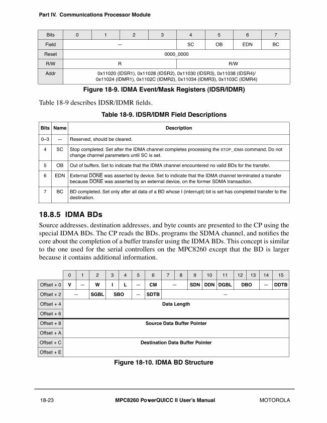
Part IV. Communications Processor Module
Table 18-9 describes IDSR/IDMR Þelds.
18.8.5 IDMA BDsSource addresses, destination addresses, and byte counts are presented to the CP using thespecial IDMA BDs. The CP reads the BDs, programs the SDMA channel, and notiÞes thecore about the completion of a buffer transfer using the IDMA BDs. This concept is similarto the one used for the serial controllers on the MPC8260 except that the BD is largerbecause it contains additional information.
Bits 0 1 2 3 4 5 6 7
Field Ñ SC OB EDN BC
Reset 0000_0000
R/W R R/W
Addr 0x11020 (IDSR1), 0x11028 (IDSR2), 0x11030 (IDSR3), 0x11038 (IDSR4)/ 0x11024 (IDMR1), 0x1102C (IDMR2), 0x11034 (IDMR3), 0x1103C (IDMR4)
Figure 18-9. IDMA Event/Mask Registers (IDSR/IDMR)
Table 18-9. IDSR/IDMR Field Descriptions
Bits Name Description
0Ð3 Ñ Reserved, should be cleared.
4 SC Stop completed. Set after the IDMA channel completes processing the STOP_IDMA command. Do not change channel parameters until SC is set.
5 OB Out of buffers. Set to indicate that the IDMA channel encountered no valid BDs for the transfer.
6 EDN External DONE was asserted by device. Set to indicate that the IDMA channel terminated a transfer because DONE was asserted by an external device, on the former SDMA transaction.
7 BC BD completed. Set only after all data of a BD whose I (interrupt) bit is set has completed transfer to the destination.
0 1 2 3 4 5 6 7 8 9 10 11 12 13 14 15
Offset + 0 V Ñ W I L Ñ CM Ñ SDN DDN DGBL DBO Ñ DDTB
Offset + 2 Ñ SGBL SBO Ñ SDTB Ñ
Offset + 4 Data Length
Offset + 6
Offset + 8 Source Data Buffer Pointer
Offset + A
Offset + C Destination Data Buffer Pointer
Offset + E
Figure 18-10. IDMA BD Structure
18-23 MPC8260 PowerQUICC II UserÕs Manual MOTOROLA
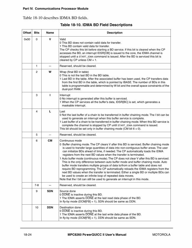
Part IV. Communications Processor Module
Table 18-10 describes IDMA BD Þelds.
Table 18-10. IDMA BD Field Descriptions
Offset Bits Name Description
0x00 0 V Valid0 This BD does not contain valid data for transfer.1 This BD contain valid data for transfer.The CP checks this bit before starting a BD service. If this bit is cleared when the CP accesses the BD, an interrupt IDSR[OB] is issued to the core, the IDMA channel is stopped until a START_IDMA command is issued. After the BD is serviced this bit is cleared by CP unless CM = 1.
1 Ñ Reserved, should be cleared.
2 W Wrap (Þnal BD in table)0 This is not the last BD in the BD table.1 Last BD in the table. After the associated buffer has been used, the CP transfers data
from the Þrst BD in the table, which is pointed by IBASE. The number of BDs in this table is programmable and determined by W bit and the overall space constraints of the dual-port RAM.
3 I Interrupt0 No interrupt is generated after this buffer is serviced. 1 When the CP services all the bufferÕs data, IDSR[BC] is set, which generates a
maskable interrupt.
4 L Last0 Not the last buffer of a chain to be transferred in buffer chaining mode. The I bit can be
used to generate an interrupt when this buffer service is complete.1 Last buffer of a chain to be transferred in buffer chaining mode. When this BD service is
complete the channel is stopped by CP until START_IDMA command is issued. This bit should be set only in buffer chaining mode (CM bit 6 = 0).
5 Ñ Reserved, should be cleared.
6 CM Continuous mode0 Buffer chaining mode. The CP clears V after this BD is serviced. Buffer chaining mode
is used to transfer large quantities of data into non-contiguous buffer areas. The user can initialize BDs ahead of time, if needed. The CP automatically loads the IDMA registers from the next BD values when the transfer is terminated.
1 Auto buffer mode (continuous mode). The CP does not clear V after this BD is serviced. This is the only difference between auto buffer mode and buffer chaining mode. Auto buffer mode transfers multiple groups of data to/from a buffer table and does not require BD reprogramming. The CP automatically reloads the IDMA registers from the next BD values when the transfer is terminated. Either a single BD or multiple BDs can be used to create an inÞnite loop of repeated data moves.
Note that the I bit can still be used to generate an interrupt in this mode.
7-8 Ñ Reserved, should be cleared.
9 SDN Source done0 DONE is inactive during this BD.1 The IDMA asserts DONE at the last read data phase of the BD.In ßy-by mode (DCM[FB] = 1), SDN should be same as DDN.
10 DDN Destination done0 DONE is inactive during this BD.1 The IDMA asserts DONE at the last write data phase of the BD.In ßy-by mode (DCM[FB] = 1), DDN should be same as SDN.
18-24 MPC8260 PowerQUICC II UserÕs Manual MOTOROLA
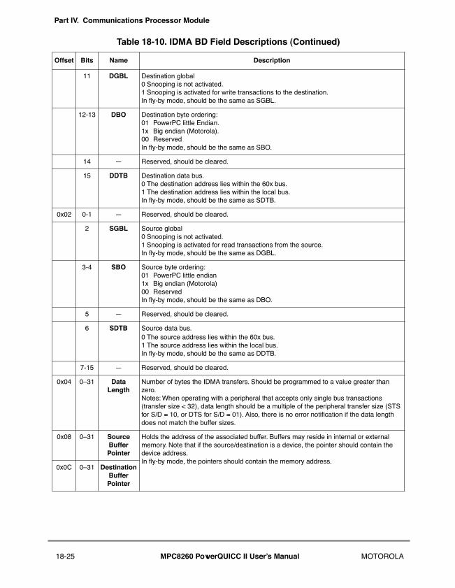
Part IV. Communications Processor Module
11 DGBL Destination global0 Snooping is not activated.1 Snooping is activated for write transactions to the destination.In ßy-by mode, should be the same as SGBL.
12-13 DBO Destination byte ordering:01 PowerPC little Endian.1x Big endian (Motorola).00 ReservedIn ßy-by mode, should be the same as SBO.
14 Ñ Reserved, should be cleared.
15 DDTB Destination data bus.0 The destination address lies within the 60x bus. 1 The destination address lies within the local bus.In ßy-by mode, should be the same as SDTB.
0x02 0-1 Ñ Reserved, should be cleared.
2 SGBL Source global 0 Snooping is not activated.1 Snooping is activated for read transactions from the source.In ßy-by mode, should be the same as DGBL.
3-4 SBO Source byte ordering:01 PowerPC little endian1x Big endian (Motorola)00 ReservedIn ßy-by mode, should be the same as DBO.
5 Ñ Reserved, should be cleared.
6 SDTB Source data bus.0 The source address lies within the 60x bus.1 The source address lies within the local bus.In ßy-by mode, should be the same as DDTB.
7-15 Ñ Reserved, should be cleared.
0x04 0Ð31 Data Length
Number of bytes the IDMA transfers. Should be programmed to a value greater than zero.Notes: When operating with a peripheral that accepts only single bus transactions (transfer size < 32), data length should be a multiple of the peripheral transfer size (STS for S/D = 10, or DTS for S/D = 01). Also, there is no error notiÞcation if the data length does not match the buffer sizes.
0x08 0Ð31 Source Buffer Pointer
Holds the address of the associated buffer. Buffers may reside in internal or external memory. Note that if the source/destination is a device, the pointer should contain the device address.In ßy-by mode, the pointers should contain the memory address.
0x0C 0Ð31 Destination Buffer Pointer
Table 18-10. IDMA BD Field Descriptions (Continued)
Offset Bits Name Description
18-25 MPC8260 PowerQUICC II UserÕs Manual MOTOROLA
Part IV. Communications Processor Module
18.9 IDMA CommandsThe user has two commands to control each IDMA channel. These commands are executedthrough the CP command register (CPCR); see Section 13.4, ÒCommand Set.Ó
18.9.1 START_IDMA CommandThe START_IDMA command is used to start a transfer on an IDMA channel. The user mustinitialize all parameters relevant for the correct operation of the channel (IDMAx_BASEand IDMA channel parameter table) before issuing this command.
To restart the channel operation, the START_IDMA command can be reissued after everypause in channel activity. The user must ensure that parameters are correct for the channelto continue operation correctly.
The parameter ISTATE of the IDMA parameter RAM should be cleared before every issueof a START_IDMA command.
An IDMA pause may occur for one of the following reasons:
¥ The channel is out of buffersÑIDSR[OB] event is set and an interrupt is generated to the core, if enabled.
¥ DONE was asserted externally and DCM[DT] = 0 (see Table 18-5). An IDSR[EDN] event is set and an interrupt is generated to the core, if enabled.
¥ STOP_IDMA command was issued.
¥ The channel has Þnished a transfer of a BD with the last bit (L) set.
If the START_IDMA command is reissued and channel has more buffers to transfer, it restartstransferring data according to the next BD in the buffer table.
In external request mode (ERM=1), the START_IDMA command initializes the channel, butthe Þrst data transfer is performed after external DREQx assertion.
In internal request mode (ERM=0), the START_IDMA command starts the data transferalmost immediately, with a delay which depends on the CP load.
18.9.2 STOP_IDMA CommandThe STOP_IDMA command is issued to stop the transfer of an IDMA channel.
When a STOP_IDMA command is issued, the CP terminates current IDMA transfers and thecurrent BD is closed (if it was open). If memory is the destination, all data in the IDMAinternal buffer is transferred to memory before termination.
At the end of the stop process, the stop-completed event (SC) is set and a maskable interruptis generated to the core. The user should not modify channel parameters until SC = 1. Whenthe channel is stopped, it does not respond to external requests. If a START_IDMA commandis reissued, the next BD in the BD table is processed (if it is valid).
18-26 MPC8260 PowerQUICC II UserÕs Manual MOTOROLA
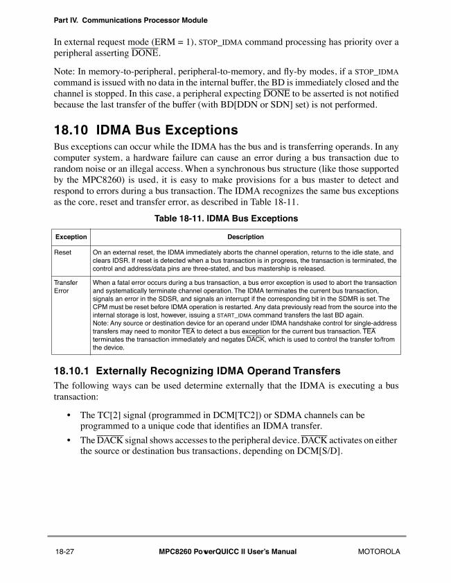
Part IV. Communications Processor Module
In external request mode (ERM = 1), STOP_IDMA command processing has priority over aperipheral asserting DONE.
Note: In memory-to-peripheral, peripheral-to-memory, and ßy-by modes, if a STOP_IDMA
command is issued with no data in the internal buffer, the BD is immediately closed and thechannel is stopped. In this case, a peripheral expecting DONE to be asserted is not notiÞedbecause the last transfer of the buffer (with BD[DDN or SDN] set) is not performed.
18.10 IDMA Bus ExceptionsBus exceptions can occur while the IDMA has the bus and is transferring operands. In anycomputer system, a hardware failure can cause an error during a bus transaction due torandom noise or an illegal access. When a synchronous bus structure (like those supportedby the MPC8260) is used, it is easy to make provisions for a bus master to detect andrespond to errors during a bus transaction. The IDMA recognizes the same bus exceptionsas the core, reset and transfer error, as described in Table 18-11.
18.10.1 Externally Recognizing IDMA Operand TransfersThe following ways can be used determine externally that the IDMA is executing a bustransaction:
¥ The TC[2] signal (programmed in DCM[TC2]) or SDMA channels can be programmed to a unique code that identiÞes an IDMA transfer.
¥ The DACK signal shows accesses to the peripheral device. DACK activates on either the source or destination bus transactions, depending on DCM[S/D].
Table 18-11. IDMA Bus Exceptions
Exception Description
Reset On an external reset, the IDMA immediately aborts the channel operation, returns to the idle state, and clears IDSR. If reset is detected when a bus transaction is in progress, the transaction is terminated, the control and address/data pins are three-stated, and bus mastership is released.
Transfer Error
When a fatal error occurs during a bus transaction, a bus error exception is used to abort the transaction and systematically terminate channel operation. The IDMA terminates the current bus transaction, signals an error in the SDSR, and signals an interrupt if the corresponding bit in the SDMR is set. The CPM must be reset before IDMA operation is restarted. Any data previously read from the source into the internal storage is lost, however, issuing a START_IDMA command transfers the last BD again.Note: Any source or destination device for an operand under IDMA handshake control for single-address transfers may need to monitor TEA to detect a bus exception for the current bus transaction. TEA terminates the transaction immediately and negates DACK, which is used to control the transfer to/from the device.
18-27 MPC8260 PowerQUICC II UserÕs Manual MOTOROLA
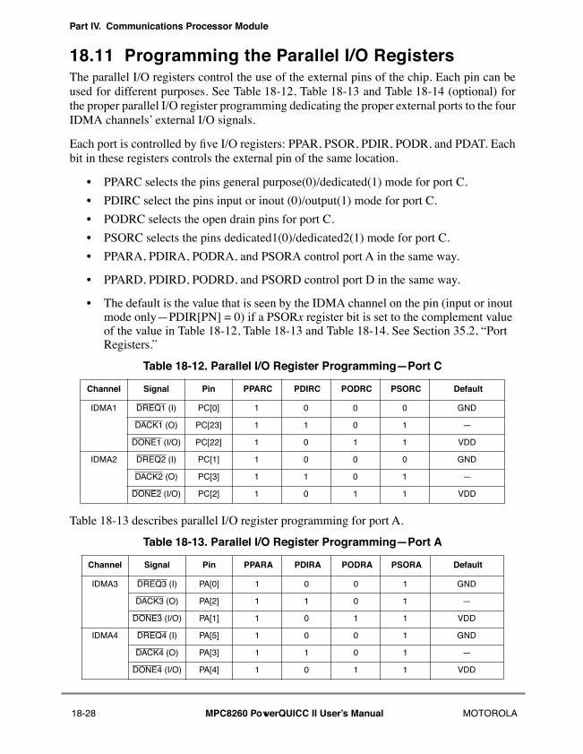
Part IV. Communications Processor Module
18.11 Programming the Parallel I/O RegistersThe parallel I/O registers control the use of the external pins of the chip. Each pin can beused for different purposes. See Table 18-12, Table 18-13 and Table 18-14 (optional) forthe proper parallel I/O register programming dedicating the proper external ports to the fourIDMA channelsÕ external I/O signals.
Each port is controlled by Þve I/O registers: PPAR, PSOR, PDIR, PODR, and PDAT. Eachbit in these registers controls the external pin of the same location.
¥ PPARC selects the pins general purpose(0)/dedicated(1) mode for port C.
¥ PDIRC select the pins input or inout (0)/output(1) mode for port C.
¥ PODRC selects the open drain pins for port C.
¥ PSORC selects the pins dedicated1(0)/dedicated2(1) mode for port C.
¥ PPARA, PDIRA, PODRA, and PSORA control port A in the same way.
¥ PPARD, PDIRD, PODRD, and PSORD control port D in the same way.
¥ The default is the value that is seen by the IDMA channel on the pin (input or inout mode onlyÑPDIR[PN] = 0) if a PSORx register bit is set to the complement value of the value in Table 18-12, Table 18-13 and Table 18-14. See Section 35.2, ÒPort Registers.Ó
Table 18-13 describes parallel I/O register programming for port A.
Table 18-12. Parallel I/O Register ProgrammingÑPort C
Channel Signal Pin PPARC PDIRC PODRC PSORC Default
IDMA1 DREQ1 (I) PC[0] 1 0 0 0 GND
DACK1 (O) PC[23] 1 1 0 1 Ñ
DONE1 (I/O) PC[22] 1 0 1 1 VDD
IDMA2 DREQ2 (I) PC[1] 1 0 0 0 GND
DACK2 (O) PC[3] 1 1 0 1 Ñ
DONE2 (I/O) PC[2] 1 0 1 1 VDD
Table 18-13. Parallel I/O Register ProgrammingÑPort A
Channel Signal Pin PPARA PDIRA PODRA PSORA Default
IDMA3 DREQ3 (I) PA[0] 1 0 0 1 GND
DACK3 (O) PA[2] 1 1 0 1 Ñ
DONE3 (I/O) PA[1] 1 0 1 1 VDD
IDMA4 DREQ4 (I) PA[5] 1 0 0 1 GND
DACK4 (O) PA[3] 1 1 0 1 Ñ
DONE4 (I/O) PA[4] 1 0 1 1 VDD
18-28 MPC8260 PowerQUICC II UserÕs Manual MOTOROLA
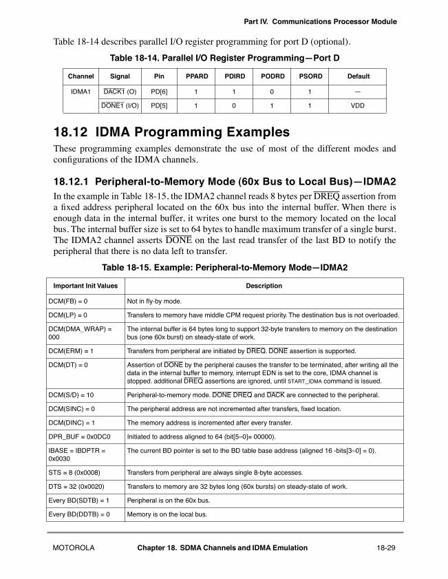
Part IV. Communications Processor Module
Table 18-14 describes parallel I/O register programming for port D (optional).
18.12 IDMA Programming ExamplesThese programming examples demonstrate the use of most of the different modes andconÞgurations of the IDMA channels.
18.12.1 Peripheral-to-Memory Mode (60x Bus to Local Bus)ÑIDMA2In the example in Table 18-15, the IDMA2 channel reads 8 bytes per DREQ assertion froma Þxed address peripheral located on the 60x bus into the internal buffer. When there isenough data in the internal buffer, it writes one burst to the memory located on the localbus. The internal buffer size is set to 64 bytes to handle maximum transfer of a single burst.The IDMA2 channel asserts DONE on the last read transfer of the last BD to notify theperipheral that there is no data left to transfer.
Table 18-14. Parallel I/O Register ProgrammingÑPort D
Channel Signal Pin PPARD PDIRD PODRD PSORD Default
IDMA1 DACK1 (O) PD[6] 1 1 0 1 Ñ
DONE1 (I/O) PD[5] 1 0 1 1 VDD
Table 18-15. Example: Peripheral-to-Memory ModeÑIDMA2
Important Init Values Description
DCM(FB) = 0 Not in ßy-by mode.
DCM(LP) = 0 Transfers to memory have middle CPM request priority. The destination bus is not overloaded.
DCM(DMA_WRAP) = 000
The internal buffer is 64 bytes long to support 32-byte transfers to memory on the destination bus (one 60x burst) on steady-state of work.
DCM(ERM) = 1 Transfers from peripheral are initiated by DREQ. DONE assertion is supported.
DCM(DT) = 0 Assertion of DONE by the peripheral causes the transfer to be terminated, after writing all the data in the internal buffer to memory, interrupt EDN is set to the core, IDMA channel is stopped. additional DREQ assertions are ignored, until START_IDMA command is issued.
DCM(S/D) = 10 Peripheral-to-memory mode. DONE DREQ and DACK are connected to the peripheral.
DCM(SINC) = 0 The peripheral address are not incremented after transfers, Þxed location.
DCM(DINC) = 1 The memory address is incremented after every transfer.
DPR_BUF = 0x0DC0 Initiated to address aligned to 64 (bit[5Ð0]= 00000).
IBASE = IBDPTR = 0x0030
The current BD pointer is set to the BD table base address (aligned 16 -bits[3Ð0] = 0).
STS = 8 (0x0008) Transfers from peripheral are always single 8-byte accesses.
DTS = 32 (0x0020) Transfers to memory are 32 bytes long (60x bursts) on steady-state of work.
Every BD(SDTB) = 1 Peripheral is on the 60x bus.
Every BD(DDTB) = 0 Memory is on the local bus.
MOTOROLA Chapter 18. SDMA Channels and IDMA Emulation 18-29
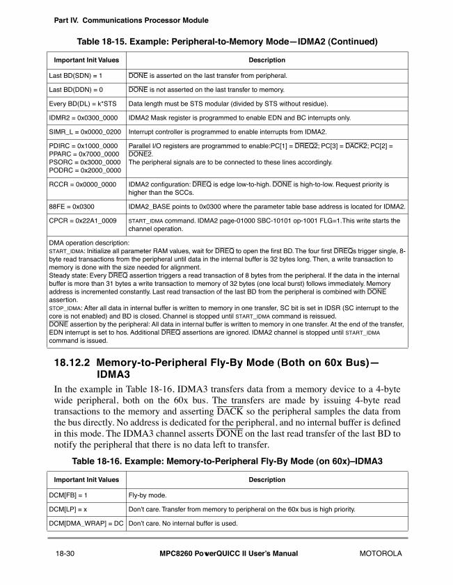
Part IV. Communications Processor Module
18.12.2 Memory-to-Peripheral Fly-By Mode (Both on 60x Bus)ÑIDMA3
In the example in Table 18-16, IDMA3 transfers data from a memory device to a 4-bytewide peripheral, both on the 60x bus. The transfers are made by issuing 4-byte readtransactions to the memory and asserting DACK so the peripheral samples the data fromthe bus directly. No address is dedicated for the peripheral, and no internal buffer is deÞnedin this mode. The IDMA3 channel asserts DONE on the last read transfer of the last BD tonotify the peripheral that there is no data left to transfer.
Last BD(SDN) = 1 DONE is asserted on the last transfer from peripheral.
Last BD(DDN) = 0 DONE is not asserted on the last transfer to memory.
Every BD(DL) = k*STS Data length must be STS modular (divided by STS without residue).
IDMR2 = 0x0300_0000 IDMA2 Mask register is programmed to enable EDN and BC interrupts only.
SIMR_L = 0x0000_0200 Interrupt controller is programmed to enable interrupts from IDMA2.
PDIRC = 0x1000_0000PPARC = 0x7000_0000 PSORC = 0x3000_0000 PODRC = 0x2000_0000
Parallel I/O registers are programmed to enable:PC[1] = DREQ2; PC[3] = DACK2; PC[2] = DONE2.The peripheral signals are to be connected to these lines accordingly.
RCCR = 0x0000_0000 IDMA2 conÞguration: DREQ is edge low-to-high. DONE is high-to-low. Request priority is higher than the SCCs.
88FE = 0x0300 IDMA2_BASE points to 0x0300 where the parameter table base address is located for IDMA2.
CPCR = 0x22A1_0009 START_IDMA command. IDMA2 page-01000 SBC-10101 op-1001 FLG=1.This write starts the channel operation.
DMA operation description:START_IDMA: Initialize all parameter RAM values, wait for DREQ to open the Þrst BD. The four Þrst DREQs trigger single, 8-byte read transactions from the peripheral until data in the internal buffer is 32 bytes long. Then, a write transaction to memory is done with the size needed for alignment.Steady state: Every DREQ assertion triggers a read transaction of 8 bytes from the peripheral. If the data in the internal buffer is more than 31 bytes a write transaction to memory of 32 bytes (one local burst) follows immediately. Memory address is incremented constantly. Last read transaction of the last BD from the peripheral is combined with DONE assertion.STOP_IDMA: After all data in internal buffer is written to memory in one transfer, SC bit is set in IDSR (SC interrupt to the core is not enabled) and BD is closed. Channel is stopped until START_IDMA command is reissued.DONE assertion by the peripheral: All data in internal buffer is written to memory in one transfer. At the end of the transfer, EDN interrupt is set to hos. Additional DREQ assertions are ignored. IDMA2 channel is stopped until START_IDMA command is issued.
Table 18-16. Example: Memory-to-Peripheral Fly-By Mode (on 60x)ÐIDMA3
Important Init Values Description
DCM[FB] = 1 Fly-by mode.
DCM[LP] = x DonÕt care. Transfer from memory to peripheral on the 60x bus is high priority.
DCM[DMA_WRAP] = DC DonÕt care. No internal buffer is used.
Table 18-15. Example: Peripheral-to-Memory ModeÑIDMA2 (Continued)
Important Init Values Description
18-30 MPC8260 PowerQUICC II UserÕs Manual MOTOROLA
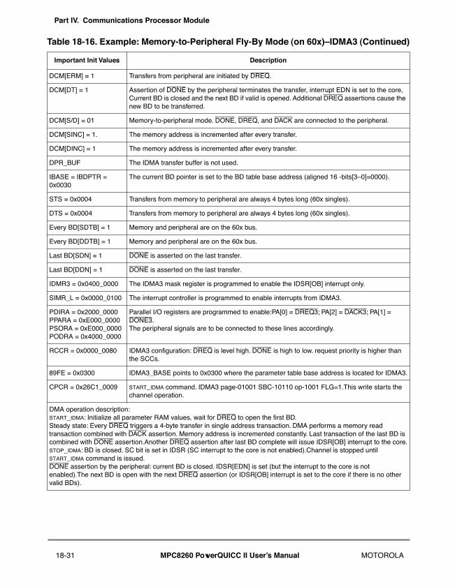
Part IV. Communications Processor Module
T
DCM[ERM] = 1 Transfers from peripheral are initiated by DREQ.
DCM[DT] = 1 Assertion of DONE by the peripheral terminates the transfer, interrupt EDN is set to the core, Current BD is closed and the next BD if valid is opened. Additional DREQ assertions cause the new BD to be transferred.
DCM[S/D] = 01 Memory-to-peripheral mode. DONE, DREQ, and DACK are connected to the peripheral.
DCM[SINC] = 1. The memory address is incremented after every transfer.
DCM[DINC] = 1 The memory address is incremented after every transfer.
DPR_BUF The IDMA transfer buffer is not used.
IBASE = IBDPTR = 0x0030
The current BD pointer is set to the BD table base address (aligned 16 -bits[3Ð0]=0000).
STS = 0x0004 Transfers from memory to peripheral are always 4 bytes long (60x singles).
DTS = 0x0004 Transfers from memory to peripheral are always 4 bytes long (60x singles).
Every BD[SDTB] = 1 Memory and peripheral are on the 60x bus.
Every BD[DDTB] = 1 Memory and peripheral are on the 60x bus.
Last BD[SDN] = 1 DONE is asserted on the last transfer.
Last BD[DDN] = 1 DONE is asserted on the last transfer.
IDMR3 = 0x0400_0000 The IDMA3 mask register is programmed to enable the IDSR[OB] interrupt only.
SIMR_L = 0x0000_0100 The interrupt controller is programmed to enable interrupts from IDMA3.
PDIRA = 0x2000_0000PPARA = 0xE000_0000 PSORA = 0xE000_0000 PODRA = 0x4000_0000
Parallel I/O registers are programmed to enable:PA[0] = DREQ3; PA[2] = DACK3; PA[1] = DONE3.The peripheral signals are to be connected to these lines accordingly.
RCCR = 0x0000_0080 IDMA3 conÞguration: DREQ is level high. DONE is high to low. request priority is higher than the SCCs.
89FE = 0x0300 IDMA3_BASE points to 0x0300 where the parameter table base address is located for IDMA3.
CPCR = 0x26C1_0009 START_IDMA command. IDMA3 page-01001 SBC-10110 op-1001 FLG=1.This write starts the channel operation.
DMA operation description:START_IDMA: Initialize all parameter RAM values, wait for DREQ to open the Þrst BD.Steady state: Every DREQ triggers a 4-byte transfer in single address transaction. DMA performs a memory read transaction combined with DACK assertion. Memory address is incremented constantly. Last transaction of the last BD is combined with DONE assertion.Another DREQ assertion after last BD complete will issue IDSR[OB] interrupt to the core.STOP_IDMA: BD is closed. SC bit is set in IDSR (SC interrupt to the core is not enabled).Channel is stopped until START_IDMA command is issued.DONE assertion by the peripheral: current BD is closed. IDSR[EDN] is set (but the interrupt to the core is not enabled).The next BD is open with the next DREQ assertion (or IDSR[OB] interrupt is set to the core if there is no other valid BDs).
able 18-16. Example: Memory-to-Peripheral Fly-By Mode (on 60x)ÐIDMA3 (Continued)
Important Init Values Description
18-31 MPC8260 PowerQUICC II UserÕs Manual MOTOROLA

Part IV. Communications Processor Module
18-32 MPC8260 PowerQUICC II UserÕs Manual MOTOROLA
Chapter 19 Serial Communications Controllers (SCCs)190190
The MPC8260 has four serial communications controllers (SCCs), which can beconÞgured independently to implement different protocols for bridging functions, routers,and gateways, and to interface with a wide variety of standard WANs, LANs, andproprietary networks. An SCC has many physical interface options such as interfacing toTDM buses, ISDN buses, and standard modem interfaces.
The SCCs are independent from the physical interface, but SCC logic formats andmanipulates data from the physical interface. Furthermore, the choice of protocol isindependent from the choice of interface. An SCC is described in terms of the protocol itruns. When an SCC is programmed to a certain protocol or mode, it implementsfunctionality that corresponds to parts of the protocolÕs link layer (layer 2 of the OSIreference model). Many SCC functions are common to protocols of the followingcontrollers:
¥ UART, described in Chapter 20, ÒSCC UART Mode.Ó
¥ HDLC and HDLC bus, described in Chapter 21, ÒSCC HDLC Mode.Ó
¥ AppleTalk/LocalTalk, described in Chapter 25, ÒSCC AppleTalk Mode.Ó
¥ BISYNC, described in Chapter 22, ÒSCC BISYNC Mode.Ó
¥ Transparent, described in Chapter 23, ÒSCC Transparent Mode.Ó
¥ Ethernet, described in Chapter 24, ÒSCC Ethernet Mode.Ó
Although the selected protocol usually applies both to the SCC transmitter and receiver, onehalf of an SCC can run transparent operations while the other runs a standard protocol(except Ethernet).
Each Rx and Tx internal clock can be programmed with either an external or internalsource. Internal clocks originate from one of eight baud rate generators (BRGs) or anexternal clock pin; see Section 15.3, ÒNMSI ConÞguration,Ó for each SCCÕs available clocksources. These clocks can be as fast as a 1:2 ratio of the system clock. (For example, an SCCinternal clock can run at 12.5 MHz in a 25-MHz system.) However, an SCCÕs ability tosupport a sustained bit stream depends on the protocol as well as other factors.
MOTOROLA Chapter 19. Serial Communications Controllers (SCCs) 19-1
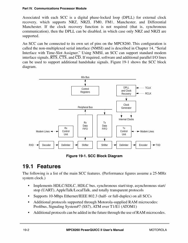
Part IV. Communications Processor Module
Associated with each SCC is a digital phase-locked loop (DPLL) for external clockrecovery, which supports NRZ, NRZI, FM0, FM1, Manchester, and DifferentialManchester. If the clock recovery function is not required (that is, synchronouscommunication), then the DPLL can be disabled, in which case only NRZ and NRZI aresupported.
An SCC can be connected to its own set of pins on the MPC8260. This conÞguration iscalled the non-multiplexed serial interface (NMSI) and is described in Chapter 14, ÒSerialInterface with Time-Slot Assigner.Ó Using NMSI, an SCC can support standard modeminterface signals, RTS, CTS, and CD. If required, software and additional parallel I/O linescan be used to support additional handshake signals. Figure 19-1 shows the SCC blockdiagram.
Figure 19-1. SCC Block Diagram
19.1 FeaturesThe following is a list of the main SCC features. (Performance Þgures assume a 25-MHzsystem clock.)
¥ Implements HDLC/SDLC, HDLC bus, synchronous start/stop, asynchronous start/stop (UART), AppleTalk/LocalTalk, and totally transparent protocols
¥ Supports 10-Mbps Ethernet/IEEE 802.3 (half- or full-duplex) on all SCCs
¥ Additional protocols supported through Motorola-supplied RAM microcodes: ProÞbus, Signaling System#7 (SS7), ATM over T1/E1 (ATOM1)
¥ Additional protocols can be added in the future through the use of RAM microcodes.
Decoder Delimiter Shifter Delimiter
Internal Clocks
Encoder
Modem LinesRx
ControlUnit
RxDataFIFO
TxDataFIFO Tx
ControlUnit
RXD
Modem Lines
ClockGenerator
DPLLand ClockRecovery
TCLK
TXD
ControlRegisters
Shifter
60x Bus
Peripheral Bus
RCLK
19-2 MPC8260 PowerQUICC II UserÕs Manual MOTOROLA
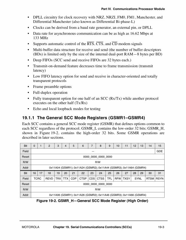
Part IV. Communications Processor Module
¥ DPLL circuitry for clock recovery with NRZ, NRZI, FM0, FM1, Manchester, and Differential Manchester (also known as Differential Bi-phase-L)
¥ Clocks can be derived from a baud rate generator, an external pin, or DPLL
¥ Data rate for asynchronous communication can be as high as 16.62 Mbps at 133 MHz
¥ Supports automatic control of the RTS, CTS, and CD modem signals
¥ Multi-buffer data structure for receive and send (the number of buffer descriptors (BDs) is limited only by the size of the internal dual-port RAMÑ8 bytes per BD)
¥ Deep FIFOs (SCC send and receive FIFOs are 32 bytes each.)
¥ Transmit-on-demand feature decreases time to frame transmission (transmit latency)
¥ Low FIFO latency option for send and receive in character-oriented and totally transparent protocols
¥ Frame preamble options
¥ Full-duplex operation
¥ Fully transparent option for one half of an SCC (Rx/Tx) while another protocol executes on the other half (Tx/Rx)
¥ Echo and local loopback modes for testing
19.1.1 The General SCC Mode Registers (GSMR1ÐGSMR4)Each SCC contains a general SCC mode register (GSMR) that deÞnes options common toeach SCC regardless of the protocol. GSMR_L contains the low-order 32 bits; GSMR_H,shown in Figure 19-2, contains the high-order 32 bits. Some GSMR operations aredescribed in later sections.
Bit 0 1 2 3 4 5 6 7 8 9 10 11 12 13 14 15
Field Ñ GDE
Reset 0000_0000_0000_0000
R/W R/W
Addr 0x11A04 (GSMR1); 0x11A24 (GSMR2); 0x11A44 (GSMR3); 0x11A64 (GSMR4)
Bit 16 17 18 19 20 21 22 23 24 25 26 27 28 29 30 31
Field TCRC REVD TRX TTX CDP CTSP CDS CTSS TFL RFW TXSY SYNL RTSM RSYN
Reset 0000_0000_0000_0000
R/W R/W
Addr 0x11A06 (GSMR1); 0x11A26 (GSMR2); 0x11A46 (GSMR3); 0x11A66 (GSMR4)
Figure 19-2. GSMR_HÑGeneral SCC Mode Register (High Order)
MOTOROLA Chapter 19. Serial Communications Controllers (SCCs) 19-3
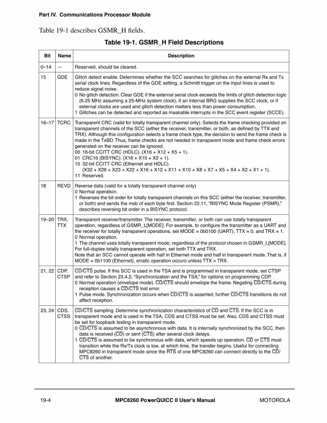
Part IV. Communications Processor Module
Table 19-1 describes GSMR_H Þelds.
Table 19-1. GSMR_H Field Descriptions
Bit Name Description
0Ð14 Ñ Reserved, should be cleared.
15 GDE Glitch detect enable. Determines whether the SCC searches for glitches on the external Rx and Tx serial clock lines. Regardless of the GDE setting, a Schmitt trigger on the input lines is used to reduce signal noise.0 No glitch detection. Clear GDE if the external serial clock exceeds the limits of glitch detection logic
(6.25 MHz assuming a 25-MHz system clock), if an internal BRG supplies the SCC clock, or if external clocks are used and glitch detection matters less than power consumption.
1 Glitches can be detected and reported as maskable interrupts in the SCC event register (SCCE).
16Ð17 TCRC Transparent CRC (valid for totally transparent channel only). Selects the frame checking provided on transparent channels of the SCC (either the receiver, transmitter, or both, as deÞned by TTX and TRX). Although this conÞguration selects a frame check type, the decision to send the frame check is made in the TxBD. Thus, frame checks are not needed in transparent mode and frame check errors generated on the receiver can be ignored.00 16-bit CCITT CRC (HDLC). (X16 + X12 + X5 + 1).01 CRC16 (BISYNC). (X16 + X15 + X2 + 1).10 32-bit CCITT CRC (Ethernet and HDLC).
(X32 + X26 + X23 + X22 + X16 + X12 + X11 + X10 + X8 + X7 + X5 + X4 + X2 + X1 + 1).11 Reserved.
18 REVD Reverse data (valid for a totally transparent channel only)0 Normal operation.1 Reverses the bit order for totally transparent channels on this SCC (either the receiver, transmitter,
or both) and sends the msb of each byte Þrst. Section 22.11, ÒBISYNC Mode Register (PSMR),Ó describes reversing bit order in a BISYNC protocol.
19Ð20 TRX, TTX
Transparent receiver/transmitter. The receiver, transmitter, or both can use totally transparent operation, regardless of GSMR_L[MODE]. For example, to conÞgure the transmitter as a UART and the receiver for totally transparent operations, set MODE = 0b0100 (UART), TTX = 0, and TRX = 1.0 Normal operation.1 The channel uses totally transparent mode, regardless of the protocol chosen in GSMR_L[MODE]. For full-duplex totally transparent operation, set both TTX and TRX.Note that an SCC cannot operate with half in Ethernet mode and half in transparent mode. That is, if MODE = 0b1100 (Ethernet), erratic operation occurs unless TTX = TRX.
21, 22 CDP, CTSP
CD/CTS pulse. If this SCC is used in the TSA and is programmed in transparent mode, set CTSP and refer to Section 23.4.2, ÒSynchronization and the TSA,Ó for options on programming CDP.0 Normal operation (envelope mode). CD/CTS should envelope the frame. Negating CD/CTS during
reception causes a CD/CTS lost error.1 Pulse mode. Synchronization occurs when CD/CTS is asserted; further CD/CTS transitions do not
affect reception.
23, 24 CDS, CTSS
CD/CTS sampling. Determine synchronization characteristics of CD and CTS. If the SCC is in transparent mode and is used in the TSA, CDS and CTSS must be set. Also, CDS and CTSS must be set for loopback testing in transparent mode.0 CD/CTS is assumed to be asynchronous with data. It is internally synchronized by the SCC, then
data is received (CD) or sent (CTS) after several clock delays.1 CD/CTS is assumed to be synchronous with data, which speeds up operation. CD or CTS must
transition while the Rx/Tx clock is low, at which time, the transfer begins. Useful for connecting MPC8260 in transparent mode since the RTS of one MPC8260 can connect directly to the CD/CTS of another.
19-4 MPC8260 PowerQUICC II UserÕs Manual MOTOROLA
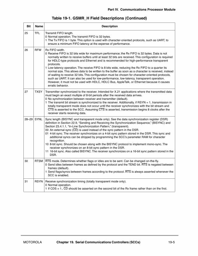
Part IV. Communications Processor Module
25 TFL Transmit FIFO length.0 Normal operation. The transmit FIFO is 32 bytes. 1 The Tx FIFO is 1 byte. This option is used with character-oriented protocols, such as UART, to
ensure a minimum FIFO latency at the expense of performance.
26 RFW Rx FIFO width. 0 Receive FIFO is 32 bits wide for maximum performance; the Rx FIFO is 32 bytes. Data is not
normally written to receive buffers until at least 32 bits are received. This conÞguration is required for HDLC-type protocols and Ethernet and is recommended for high-performance transparent protocols.
1 Low-latency operation. The receive FIFO is 8 bits wide, reducing the Rx FIFO to a quarter its normal size. This allows data to be written to the buffer as soon as a character is received, instead of waiting to receive 32 bits. This conÞguration must be chosen for character-oriented protocols, such as UART. It can also be used for low-performance, low-latency, transparent operation. However, it must not be used with HDLC, HDLC Bus, AppleTalk, or Ethernet because it causes erratic behavior.
27 TXSY Transmitter synchronized to the receiver. Intended for X.21 applications where the transmitted data must begin an exact multiple of 8-bit periods after the received data arrives.0 No synchronization between receiver and transmitter (default).1 The transmit bit stream is synchronized to the receiver. Additionally, if RSYN = 1, transmission in
totally transparent mode does not occur until the receiver synchronizes with the bit stream and CTS is asserted to the SCC. Assuming CTS is asserted, transmission begins 8 clocks after the receiver starts receiving data.
28Ð29 SYNL Sync length (BISYNC and transparent mode only). See the data synchronization register (DSR) deÞnition in Section 22.9, ÒSending and Receiving the Synchronization Sequence,Ó (BISYNC) and Section 23.4.1.1, ÒIn-Line Synchronization Pattern,Ó (transparent). 00 An external sync (CD) is used instead of the sync pattern in the DSR.01 4-bit sync. The receiver synchronizes on a 4-bit sync pattern stored in the DSR. This sync and
additional syncs can be stripped by programming the SCCÕs parameter RAM for character recognition.
10 8-bit sync. Should be chosen along with the BISYNC protocol to implement mono-sync. The receiver synchronizes on an 8-bit sync pattern in the DSR.
11 16-bit sync. Also called BISYNC. The receiver synchronizes on a 16-bit sync pattern stored in the DSR.
30 RTSM RTS mode. Determines whether ßags or idles are to be sent. Can be changed on-the-ßy. 0 Send idles between frames as deÞned by the protocol and the TEND bit. RTS is negated between
frames (default).1 Send ßags/syncs between frames according to the protocol. RTS is always asserted whenever the
SCC is enabled.
31 RSYN Receive synchronization timing (totally transparent mode only). 0 Normal operation. 1 If CDS = 1, CD should be asserted on the second bit of the Rx frame rather than on the Þrst.
Table 19-1. GSMR_H Field Descriptions (Continued)
Bit Name Description
MOTOROLA Chapter 19. Serial Communications Controllers (SCCs) 19-5
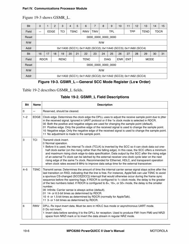
Part IV. Communications Processor Module
Figure 19-3 shows GSMR_L.
Table 19-2 describes GSMR_L Þelds.
Bit 0 1 2 3 4 5 6 7 8 9 10 11 12 13 14 15
Field Ñ EDGE TCI TSNC RINV TINV TPL TPP TEND TDCR
Reset 0000_0000_0000_0000
R/W R/W
Addr 0x11A00 (SCC1); 0x11A20 (SCC2); 0x11A40 (SCC3); 0x11A60 (SCC4)
Bit 16 17 18 19 20 21 22 23 24 25 26 27 28 29 30 31
Field RDCR RENC TENC DIAG ENR ENT MODE
Reset 0000_0000_0000_0000
R/W R/W
Addr 0x11A02 (SCC1); 0x11A22 (SCC2); 0x11A42 (SCC3); 0x11A62 (SCC4)
Figure 19-3. GSMR_LÑGeneral SCC Mode Register (Low Order)
Table 19-2. GSMR_L Field Descriptions
Bit Name Description
0 Ñ Reserved, should be cleared.
1Ð2 EDGE Clock edge. Determines the clock edge the DPLL uses to adjust the receive sample point due to jitter in the received signal. Ignored in UART protocol or if the 1x clock mode is selected in RDCR.00 Both the positive and negative edges are used for changing the sample point (default).01 Positive edge. Only the positive edge of the received signal is used to change the sample point.10 Negative edge. Only the negative edge of the received signal is used to change the sample point.11 No adjustment is made to the sample point.
3 TCI Transmit clock invert. 0 Normal operation.1 Before it is used, the internal Tx clock (TCLK) is inverted by the SCC so it can clock data out one-
half clock earlier (on the rising rather than the falling edge). In this case, the SCC offers a minimum and maximum rising clock edge-to-data speciÞcation. Data output by the SCC after the rising edge of an external Tx clock can be latched by the external receiver one clock cycle later on the next rising edge of the same Tx clock. Recommended for Ethernet, HDLC, and transparent operation when clock rates exceed 8 MHz to improve data setup time for the external transceiver.
4Ð5 TSNC Transmit sense. Determines the amount of time the internal carrier sense signal stays active after the last transition on RXD, indicating that the line is free. For instance, AppleTalk can use TSNC to avoid a spurious CS-changed (SCCE[DCC]) interrupt that would otherwise occur during the frame sync sequence before the opening ßags. If RDCR is conÞgured to 1´ clock mode, the delay is the greater of the two numbers listed. If RDCR is conÞgured to 8´, 16´, or 32´ mode, the delay is the smaller number.00 InÞnite. Carrier sense is always active (default).01 14- or 6.5-bit times as determined by RDCR.10 4- or 1.5-bit times as determined by RDCR (normally for AppleTalk).11 3- or 1-bit times as determined by RDCR.
6 RINV DPLL Rx input invert data. Must be zero in HDLC bus mode or asynchronous UART mode.0 Do not invert.1 Invert data before sending it to the DPLL for reception. Used to produce FM1 from FM0 and NRZI
space from NRZI mark or to invert the data stream in regular NRZ mode.
19-6 MPC8260 PowerQUICC II UserÕs Manual MOTOROLA
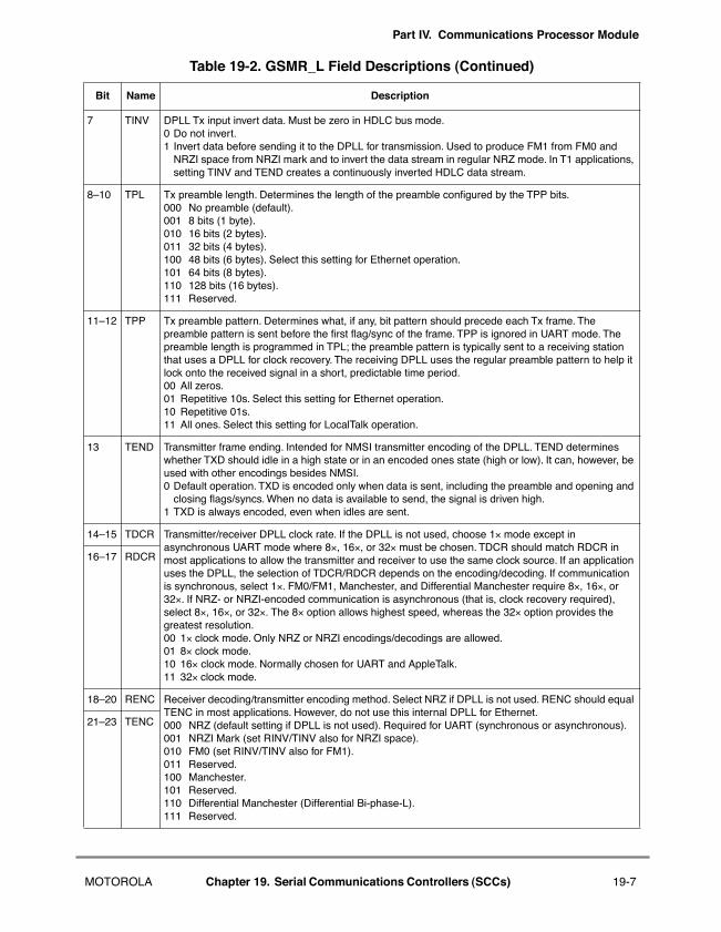
Part IV. Communications Processor Module
7 TINV DPLL Tx input invert data. Must be zero in HDLC bus mode.0 Do not invert.1 Invert data before sending it to the DPLL for transmission. Used to produce FM1 from FM0 and
NRZI space from NRZI mark and to invert the data stream in regular NRZ mode. In T1 applications, setting TINV and TEND creates a continuously inverted HDLC data stream.
8Ð10 TPL Tx preamble length. Determines the length of the preamble conÞgured by the TPP bits.000 No preamble (default).001 8 bits (1 byte).010 16 bits (2 bytes).011 32 bits (4 bytes).100 48 bits (6 bytes). Select this setting for Ethernet operation.101 64 bits (8 bytes).110 128 bits (16 bytes).111 Reserved.
11Ð12 TPP Tx preamble pattern. Determines what, if any, bit pattern should precede each Tx frame. The preamble pattern is sent before the Þrst ßag/sync of the frame. TPP is ignored in UART mode. The preamble length is programmed in TPL; the preamble pattern is typically sent to a receiving station that uses a DPLL for clock recovery. The receiving DPLL uses the regular preamble pattern to help it lock onto the received signal in a short, predictable time period.00 All zeros.01 Repetitive 10s. Select this setting for Ethernet operation.10 Repetitive 01s.11 All ones. Select this setting for LocalTalk operation.
13 TEND Transmitter frame ending. Intended for NMSI transmitter encoding of the DPLL. TEND determines whether TXD should idle in a high state or in an encoded ones state (high or low). It can, however, be used with other encodings besides NMSI.0 Default operation. TXD is encoded only when data is sent, including the preamble and opening and
closing ßags/syncs. When no data is available to send, the signal is driven high.1 TXD is always encoded, even when idles are sent.
14Ð15 TDCR Transmitter/receiver DPLL clock rate. If the DPLL is not used, choose 1´ mode except in asynchronous UART mode where 8´, 16´, or 32´ must be chosen. TDCR should match RDCR in most applications to allow the transmitter and receiver to use the same clock source. If an application uses the DPLL, the selection of TDCR/RDCR depends on the encoding/decoding. If communication is synchronous, select 1´. FM0/FM1, Manchester, and Differential Manchester require 8´, 16´, or 32´. If NRZ- or NRZI-encoded communication is asynchronous (that is, clock recovery required), select 8´, 16´, or 32´. The 8´ option allows highest speed, whereas the 32´ option provides the greatest resolution.00 1´ clock mode. Only NRZ or NRZI encodings/decodings are allowed.01 8´ clock mode.10 16´ clock mode. Normally chosen for UART and AppleTalk.11 32´ clock mode.
16Ð17 RDCR
18Ð20 RENC Receiver decoding/transmitter encoding method. Select NRZ if DPLL is not used. RENC should equal TENC in most applications. However, do not use this internal DPLL for Ethernet.000 NRZ (default setting if DPLL is not used). Required for UART (synchronous or asynchronous).001 NRZI Mark (set RINV/TINV also for NRZI space).010 FM0 (set RINV/TINV also for FM1).011 Reserved.100 Manchester.101 Reserved.110 Differential Manchester (Differential Bi-phase-L).111 Reserved.
21Ð23 TENC
Table 19-2. GSMR_L Field Descriptions (Continued)
Bit Name Description
MOTOROLA Chapter 19. Serial Communications Controllers (SCCs) 19-7
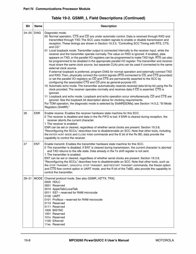
Part IV. Communications Processor Module
24Ð25 DIAG Diagnostic mode. 00 Normal operation, CTS and CD are under automatic control. Data is received through RXD and
transmitted through TXD. The SCC uses modem signals to enable or disable transmission and reception. These timings are shown in Section 19.3.5, ÒControlling SCC Timing with RTS, CTS, and CD.Ó
01 Local loopback mode. Transmitter output is connected internally to the receiver input, while the receiver and the transmitter operate normally. The value on RXD is ignored. If enabled, data appears on TXD, or the parallel I/O registers can be programmed to make TXD high. RTS can also be programmed to be disabled in the appropriate parallel I/O register. The transmitter and receiver must share the same clock source, but separate CLKx pins can be used if connected to the same external clock source.If external loopback is preferred, program DIAG for normal operation and externally connect TXD and RXD. Then, physically connect the control signals (RTS connected to CD, and CTS grounded) or set the parallel I/O registers so CD and CTS are permanently asserted to the SCC by conÞguring the associated CTS and CD pins as general-purpose I/O.
10 Automatic echo mode. The transmitter automatically resends received data bit-by-bit using the Rx clock provided. The receiver operates normally and receives data if CD is asserted. CTS is ignored.
11 Loopback and echo mode. Loopback and echo operation occur simultaneously. CD and CTS are ignored. See the loopback bit description above for clocking requirements.
For TDM operation, the diagnostic mode is selected by SIxMR[SDMx]; see Section 14.5.2, ÒSI Mode Registers (SIxMR).Ó
26 ENR Enable receive. Enables the receiver hardware state machine for this SCC. 0 The receiver is disabled and data in the Rx FIFO is lost. If ENR is cleared during reception, the
receiver aborts the current character.1 The receiver is enabled. ENR can be set or cleared, regardless of whether serial clocks are present. Section 19.3.8, ÒReconÞguring the SCCs,Ó describes how to disable/enable an SCC. Note that other tools, including the ENTER HUNT MODE and CLOSE RXBD commands and the E bit of the Rx BD, data provide the capability to control the receiver.
27 ENT Enable transmit. Enables the transmitter hardware state machine for this SCC.0 The transmitter is disabled. If ENT is cleared during transmission, the current character is aborted
and TXD returns to the idle state. Data already in the Tx shift register is not sent. 1 The transmitter is enabled. ENT can be set or cleared, regardless of whether serial clocks are present. Section 19.3.8, ÒReconÞguring the SCCs,Ó describes how to disable/enable an SCC. Note that other tools, such as the STOP TRANSMIT, GRACEFUL STOP TRANSMIT, and RESTART TRANSMIT commands, the freeze option and CTS ßow control option in UART mode, and the R bit of the TxBD, also provide the capability to control the transmitter.
28Ð31 MODE Channel protocol mode. See also GSMR_H[TTX, TRX].0000 HDLC0001 Reserved0010 AppleTalk/LocalTalk0011 SS7Ñreserved for RAM microcode0100 UART0101 ProÞbusÑreserved for RAM microcode0110 Reserved0111 Reserved1000 BISYNC1001 Reserved101x Reserved1100 Ethernet 11xx Reserved
Table 19-2. GSMR_L Field Descriptions (Continued)
Bit Name Description
19-8 MPC8260 PowerQUICC II UserÕs Manual MOTOROLA
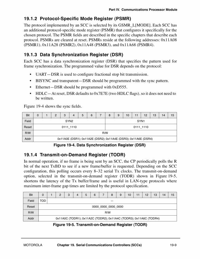
Part IV. Communications Processor Module
19.1.2 Protocol-SpeciÞc Mode Register (PSMR)The protocol implemented by an SCC is selected by its GSMR_L[MODE]. Each SCC hasan additional protocol-speciÞc mode register (PSMR) that conÞgures it speciÞcally for thechosen protocol. The PSMR Þelds are described in the speciÞc chapters that describe eachprotocol. PSMRs are cleared at reset. PSMRs reside at the following addresses: 0x11A08(PSMR1), 0x11A28 (PSMR2), 0x11A48 (PSMR3), and 0x11A68 (PSMR4).
19.1.3 Data Synchronization Register (DSR)Each SCC has a data synchronization register (DSR) that speciÞes the pattern used forframe synchronization. The programmed value for DSR depends on the protocol:
¥ UARTÑDSR is used to conÞgure fractional stop bit transmission.
¥ BISYNC and transparentÑDSR should be programmed with the sync pattern.
¥ EthernetÑDSR should be programmed with 0xD555.
¥ HDLCÑAt reset, DSR defaults to 0x7E7E (two HDLC ßags), so it does not need to be written.
Figure 19-4 shows the sync Þelds.
19.1.4 Transmit-on-Demand Register (TODR)In normal operation, if no frame is being sent by an SCC, the CP periodically polls the Rbit of the next TxBD to see if a new frame/buffer is requested. Depending on the SCCconÞguration, this polling occurs every 8Ð32 serial Tx clocks. The transmit-on-demandoption, selected in the transmit-on-demand register (TODR) shown in Figure 19-5,shortens the latency of the Tx buffer/frame and is useful in LAN-type protocols wheremaximum inter-frame gap times are limited by the protocol speciÞcation.
Bit 0 1 2 3 4 5 6 7 8 9 10 11 12 13 14 15
Field SYN2 SYN1
Reset 0111_1110 0111_1110
R/W R/W
Addr 0x11A0E (DSR1); 0x11A2E (DSR2); 0x11A4E (DSR3); 0x11A6E (DSR4)
Figure 19-4. Data Synchronization Register (DSR)
Bit 0 1 2 3 4 5 6 7 8 9 10 11 12 13 14 15
Field TOD Ñ
Reset 0000_0000_0000_0000
R/W R/W
Addr 0x11A0C (TODR1); 0x11A2C (TODR2); 0x11A4C (TODR3); 0x11A6C (TODR4)
Figure 19-5. Transmit-on-Demand Register (TODR)
MOTOROLA Chapter 19. Serial Communications Controllers (SCCs) 19-9
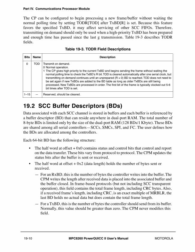
Part IV. Communications Processor Module
The CP can be conÞgured to begin processing a new frame/buffer without waiting thenormal polling time by setting TODR[TOD] after TxBD[R] is set. Because this featurefavors the speciÞed TxBD, it may affect servicing of other SCC FIFOs. Therefore,transmitting on demand should only be used when a high-priority TxBD has been preparedand enough time has passed since the last g transmission. Table 19-3 describes TODRÞelds.
19.2 SCC Buffer Descriptors (BDs)Data associated with each SCC channel is stored in buffers and each buffer is referenced bya buffer descriptor (BD) that can reside anywhere in dual-port RAM. The total number of8-byte BDs is limited only by the size of the dual-port RAM (128 BDs/1 Kbyte). These BDsare shared among all serial controllersÑSCCs, SMCs, SPI, and I2C. The user deÞnes howthe BDs are allocated among the controllers.
Each 64-bit BD has the following structure:
¥ The half word at offset + 0x0 contains status and control bits that control and report on the data transfer. These bits vary from protocol to protocol. The CPM updates the status bits after the buffer is sent or received.
¥ The half word at offset + 0x2 (data length) holds the number of bytes sent or received.
Ñ For an RxBD, this is the number of bytes the controller writes into the buffer. The CPM writes the length after received data is placed into the associated buffer and the buffer closed. In frame-based protocols (but not including SCC transparent operation), this Þeld contains the total frame length, including CRC bytes. Also, if a received frameÕs length, including CRC, is an exact multiple of MRBLR, the last BD holds no actual data but does contain the total frame length.
Ñ For a TxBD, this is the number of bytes the controller should send from its buffer. Normally, this value should be greater than zero. The CPM never modiÞes this Þeld.
Table 19-3. TODR Field Descriptions
Bits Name Description
0 TOD Transmit on demand. 0 Normal operation.1 The CP gives high priority to the current TxBD and begins sending the frame without waiting the
normal polling time to check the TxBDÕs R bit. TOD is cleared automatically after one serial clock, but transmitting on demand continues until an unprepared (R = 0) BD is reached. TOD does not need to be set again if new TxBDs are added to the BD table as long as older TxBDs are still being processed. New TxBDs are processed in order. The Þrst bit of the frame is typically clocked out 5-6 bit times after TOD is set.
1Ð15 Ñ Reserved, should be cleared.
19-10 MPC8260 PowerQUICC II UserÕs Manual MOTOROLA
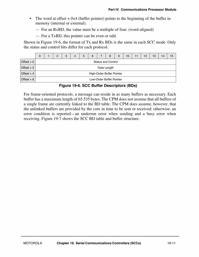
Part IV. Communications Processor Module
¥ The word at offset + 0x4 (buffer pointer) points to the beginning of the buffer in memory (internal or external).
Ñ For an RxBD, the value must be a multiple of four. (word-aligned)
Ñ For a TxBD, this pointer can be even or odd.
Shown in Figure 19-6, the format of Tx and Rx BDs is the same in each SCC mode. Onlythe status and control bits differ for each protocol.
For frame-oriented protocols, a message can reside in as many buffers as necessary. Eachbuffer has a maximum length of 65,535 bytes. The CPM does not assume that all buffers ofa single frame are currently linked to the BD table. The CPM does assume, however, thatthe unlinked buffers are provided by the core in time to be sent or received; otherwise, anerror condition is reportedÑan underrun error when sending and a busy error whenreceiving. Figure 19-7 shows the SCC BD table and buffer structure.
0 1 2 3 4 5 6 7 8 9 10 11 12 13 14 15
Offset + 0 Status and Control
Offset + 2 Data Length
Offset + 4 High-Order Buffer Pointer
Offset + 6 Low-Order Buffer Pointer
Figure 19-6. SCC Buffer Descriptors (BDs)
MOTOROLA Chapter 19. Serial Communications Controllers (SCCs) 19-11
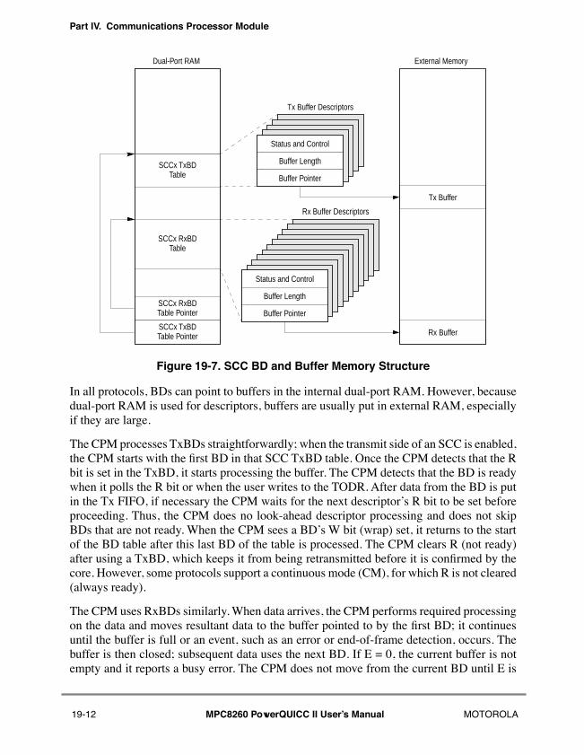
Part IV. Communications Processor Module
Figure 19-7. SCC BD and Buffer Memory Structure
In all protocols, BDs can point to buffers in the internal dual-port RAM. However, becausedual-port RAM is used for descriptors, buffers are usually put in external RAM, especiallyif they are large.
The CPM processes TxBDs straightforwardly; when the transmit side of an SCC is enabled,the CPM starts with the Þrst BD in that SCC TxBD table. Once the CPM detects that the Rbit is set in the TxBD, it starts processing the buffer. The CPM detects that the BD is readywhen it polls the R bit or when the user writes to the TODR. After data from the BD is putin the Tx FIFO, if necessary the CPM waits for the next descriptorÕs R bit to be set beforeproceeding. Thus, the CPM does no look-ahead descriptor processing and does not skipBDs that are not ready. When the CPM sees a BDÕs W bit (wrap) set, it returns to the startof the BD table after this last BD of the table is processed. The CPM clears R (not ready)after using a TxBD, which keeps it from being retransmitted before it is conÞrmed by thecore. However, some protocols support a continuous mode (CM), for which R is not cleared(always ready).
The CPM uses RxBDs similarly. When data arrives, the CPM performs required processingon the data and moves resultant data to the buffer pointed to by the Þrst BD; it continuesuntil the buffer is full or an event, such as an error or end-of-frame detection, occurs. Thebuffer is then closed; subsequent data uses the next BD. If E = 0, the current buffer is notempty and it reports a busy error. The CPM does not move from the current BD until E is
Status and Control
Buffer Length
Buffer Pointer
SCCx TxBDTable Pointer
SCCx RxBDTable Pointer
SCCx RxBDTable
SCCx TxBDTable
Dual-Port RAM
Status and Control
Buffer Length
Buffer Pointer
Tx Buffer
External Memory
Rx Buffer Descriptors
Tx Buffer Descriptors
Rx Buffer
19-12 MPC8260 PowerQUICC II UserÕs Manual MOTOROLA
Part IV. Communications Processor Module
set by the core (the buffer is empty). After using a descriptor, the CPM clears E (not empty)and does not reuse a BD until it has been processed by the core. However, in continuousmode (CM), E remains set. When the CPM discovers a descriptorÕs W bit set (indicating itis the last BD in the circular BD table), it returns to the beginning of the table when it istime to move to the next buffer.
19.3 SCC Parameter RAMEach SCC parameter RAM area begins at the same offset from each SCC base area.Section 19.3.1, ÒSCC Base Addresses,Ó describes the SCCÕs base addresses. The protocol-speciÞc portions of the SCC parameter RAM are discussed in the speciÞc protocoldescriptions and the part that is common to all SCC protocols is shown in Table 19-4.
Some parameter RAM values must be initialized before the SCC can be enabled. Othervalues are initialized or written by the CPM. Once initialized, most parameter RAM valuesdo not need to be accessed because most activity centers around the descriptors rather thanthe parameter RAM. However, if the parameter RAM is accessed, note the following:
¥ Parameter RAM can be read at any time.
¥ Tx parameter RAM can be written only when the transmitter is disabledÑafter a STOP TRANSMIT command and before a RESTART TRANSMIT command or after the buffer/frame Þnishes transmitting after a GRACEFUL STOP TRANSMIT command and before a RESTART TRANSMIT command.
¥ Rx parameter RAM can be written only when the receiver is disabled. Note the CLOSE RXBD command does not stop reception, but it does allow the user to extract data from a partially full Rx buffer.
¥ See Section 19.3.8, ÒReconÞguring the SCCs.Ó
Table 19-4 shows the parameter RAM map for all SCC protocols. Boldfaced entries mustbe initialized by the user.
Table 19-4. SCC Parameter RAM Map for All Protocols
Offset 1 Name Width Description
0x00 RBASE Hword Rx/TxBD table base addressÑoffset from the beginning of dual-port RAM. The BD tables can be placed in any unused portion of the dual-port RAM. The CPM starts BD processing at the top of the table. (The user deÞnes the end of the BD table by setting the W bit in the last BD to be processed.) Initialize these entries before enabling the corresponding channel. Erratic operations occur if BD tables of active SCCs overlap.Values in RBASE and TBASE should be multiples of eight.
0x02 TBASE Hword
0x04 RFCR Byte Rx function code. See Section 19.3.2, ÒFunction Code Registers (RFCR and TFCR).Ó
0x05 TFCR Byte Tx function code. See Section 19.3.2, ÒFunction Code Registers (RFCR and TFCR).Ó
MOTOROLA Chapter 19. Serial Communications Controllers (SCCs) 19-13
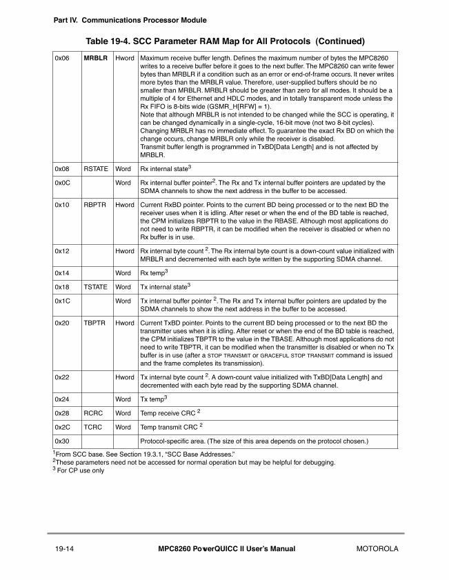
Part IV. Communications Processor Module
0x06 MRBLR Hword Maximum receive buffer length. DeÞnes the maximum number of bytes the MPC8260 writes to a receive buffer before it goes to the next buffer. The MPC8260 can write fewer bytes than MRBLR if a condition such as an error or end-of-frame occurs. It never writes more bytes than the MRBLR value. Therefore, user-supplied buffers should be no smaller than MRBLR. MRBLR should be greater than zero for all modes. It should be a multiple of 4 for Ethernet and HDLC modes, and in totally transparent mode unless the Rx FIFO is 8-bits wide (GSMR_H[RFW] = 1).Note that although MRBLR is not intended to be changed while the SCC is operating, it can be changed dynamically in a single-cycle, 16-bit move (not two 8-bit cycles). Changing MRBLR has no immediate effect. To guarantee the exact Rx BD on which the change occurs, change MRBLR only while the receiver is disabled.Transmit buffer length is programmed in TxBD[Data Length] and is not affected by MRBLR.
0x08 RSTATE Word Rx internal state3
0x0C Word Rx internal buffer pointer2. The Rx and Tx internal buffer pointers are updated by the SDMA channels to show the next address in the buffer to be accessed.
0x10 RBPTR Hword Current RxBD pointer. Points to the current BD being processed or to the next BD the receiver uses when it is idling. After reset or when the end of the BD table is reached, the CPM initializes RBPTR to the value in the RBASE. Although most applications do not need to write RBPTR, it can be modiÞed when the receiver is disabled or when no Rx buffer is in use.
0x12 Hword Rx internal byte count 2. The Rx internal byte count is a down-count value initialized with MRBLR and decremented with each byte written by the supporting SDMA channel.
0x14 Word Rx temp3
0x18 TSTATE Word Tx internal state3
0x1C Word Tx internal buffer pointer 2. The Rx and Tx internal buffer pointers are updated by the SDMA channels to show the next address in the buffer to be accessed.
0x20 TBPTR Hword Current TxBD pointer. Points to the current BD being processed or to the next BD the transmitter uses when it is idling. After reset or when the end of the BD table is reached, the CPM initializes TBPTR to the value in the TBASE. Although most applications do not need to write TBPTR, it can be modiÞed when the transmitter is disabled or when no Tx buffer is in use (after a STOP TRANSMIT or GRACEFUL STOP TRANSMIT command is issued and the frame completes its transmission).
0x22 Hword Tx internal byte count 2. A down-count value initialized with TxBD[Data Length] and decremented with each byte read by the supporting SDMA channel.
0x24 Word Tx temp3
0x28 RCRC Word Temp receive CRC 2
0x2C TCRC Word Temp transmit CRC 2
0x30 Protocol-speciÞc area. (The size of this area depends on the protocol chosen.)
1From SCC base. See Section 19.3.1, ÒSCC Base Addresses.Ó2These parameters need not be accessed for normal operation but may be helpful for debugging.3 For CP use only
Table 19-4. SCC Parameter RAM Map for All Protocols (Continued)
19-14 MPC8260 PowerQUICC II UserÕs Manual MOTOROLA
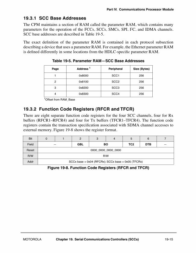
Part IV. Communications Processor Module
19.3.1 SCC Base AddressesThe CPM maintains a section of RAM called the parameter RAM, which contains manyparameters for the operation of the FCCs, SCCs, SMCs, SPI, I2C, and IDMA channels.SCC base addresses are described in Table 19-5.
The exact deÞnition of the parameter RAM is contained in each protocol subsectiondescribing a device that uses a parameter RAM. For example, the Ethernet parameter RAMis deÞned differently in some locations from the HDLC-speciÞc parameter RAM.
19.3.2 Function Code Registers (RFCR and TFCR)There are eight separate function code registers for the four SCC channels, four for Rxbuffers (RFCR1ÐRFCR4) and four for Tx buffers (TFCR1ÐTFCR4). The function coderegisters contain the transaction speciÞcation associated with SDMA channel accesses toexternal memory. Figure 19-8 shows the register format.
Table 19-5. Parameter RAMÑSCC Base Addresses
Page Address 1
1Offset from RAM_Base
Peripheral Size (Bytes)
1 0x8000 SCC1 256
2 0x8100 SCC2 256
3 0x8200 SCC3 256
4 0x8300 SCC4 256
Bit 0 1 2 3 4 5 6 7
Field Ñ GBL BO TC2 DTB Ñ
Reset 0000_0000_0000_0000
R/W R/W
Addr SCCx base + 0x04 (RFCRx); SCCx base + 0x05 (TFCRx)
Figure 19-8. Function Code Registers (RFCR and TFCR)
MOTOROLA Chapter 19. Serial Communications Controllers (SCCs) 19-15
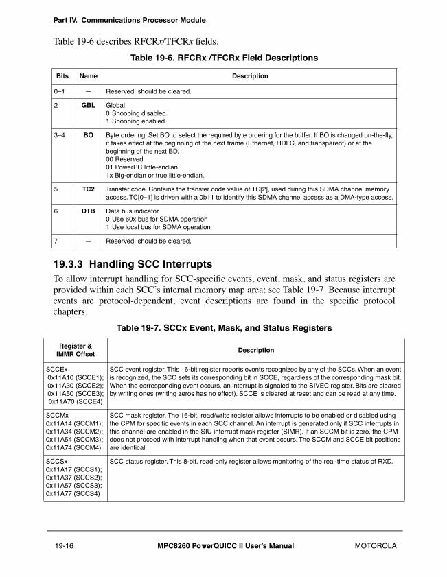
Part IV. Communications Processor Module
S
S0000
S0000
Table 19-6 describes RFCRx/TFCRx Þelds.
19.3.3 Handling SCC InterruptsTo allow interrupt handling for SCC-speciÞc events, event, mask, and status registers areprovided within each SCCÕs internal memory map area; see Table 19-7. Because interruptevents are protocol-dependent, event descriptions are found in the speciÞc protocolchapters.
Table 19-6. RFCRx /TFCRx Field Descriptions
Bits Name Description
0Ð1 Ñ Reserved, should be cleared.
2 GBL Global0 Snooping disabled. 1 Snooping enabled.
3Ð4 BO Byte ordering. Set BO to select the required byte ordering for the buffer. If BO is changed on-the-ßy, it takes effect at the beginning of the next frame (Ethernet, HDLC, and transparent) or at the beginning of the next BD.00 Reserved01 PowerPC little-endian. 1x Big-endian or true little-endian.
5 TC2 Transfer code. Contains the transfer code value of TC[2], used during this SDMA channel memory access. TC[0Ð1] is driven with a 0b11 to identify this SDMA channel access as a DMA-type access.
6 DTB Data bus indicator0 Use 60x bus for SDMA operation1 Use local bus for SDMA operation
7 Ñ Reserved, should be cleared.
Table 19-7. SCCx Event, Mask, and Status Registers
Register &IMMR Offset
Description
CCEx0x11A10 (SCCE1); 0x11A30 (SCCE2); 0x11A50 (SCCE3); 0x11A70 (SCCE4)
SCC event register. This 16-bit register reports events recognized by any of the SCCs. When an event is recognized, the SCC sets its corresponding bit in SCCE, regardless of the corresponding mask bit. When the corresponding event occurs, an interrupt is signaled to the SIVEC register. Bits are cleared by writing ones (writing zeros has no effect). SCCE is cleared at reset and can be read at any time.
CCMxx11A14 (SCCM1); x11A34 (SCCM2); x11A54 (SCCM3); x11A74 (SCCM4)
SCC mask register. The 16-bit, read/write register allows interrupts to be enabled or disabled using the CPM for speciÞc events in each SCC channel. An interrupt is generated only if SCC interrupts in this channel are enabled in the SIU interrupt mask register (SIMR). If an SCCM bit is zero, the CPM does not proceed with interrupt handling when that event occurs. The SCCM and SCCE bit positions are identical.
CCSxx11A17 (SCCS1); x11A37 (SCCS2); x11A57 (SCCS3); x11A77 (SCCS4)
SCC status register. This 8-bit, read-only register allows monitoring of the real-time status of RXD.
19-16 MPC8260 PowerQUICC II UserÕs Manual MOTOROLA
Part IV. Communications Processor Module
Follow these steps to handle an SCC interrupt:
1. When an interrupt occurs, read SCCE to determine the interrupt sources and clear those SCCE bits (in most cases).
2. Process the TxBDs to reuse them if SCCE[TX] or SCCE[TXE] = 1. If the transmit speed is fast or the interrupt delay is long, the SCC may have sent more than one Tx buffer. Thus, it is important to check more than one TxBD during interrupt handling. A common practice is to process all TxBDs in the handler until one is found with its R bit set.
3. Extract data from the RxBD if SCCE[RX], SCCE[RXB], or SCCE[RXF] is set. As with transmit buffers, if the receive speed is fast or the interrupt delay is long, the SCC may have received more than one buffer and the handler should check more than one RxBD. A common practice is to process all RxBDs in the interrupt handler until one is found with RxBD[E] set.
4. Execute the rÞ instruction.
Additional information about interrupt handling can be found in Section 4.2, ÒInterruptController.Ó
19.3.4 Initializing the SCCsThe SCCs require that a number of registers and parameters be conÞgured after a power-onreset. Regardless of the protocol used, follow these steps to initialize SCCs:
1. Write the parallel I/O ports to conÞgure and connect the I/O pins to the SCCs.
2. ConÞgure the parallel I/O registers to enable RTS, CTS, and CD if these signals are required.
3. If the time-slot assigner (TSA) is used, the serial interface (SIx) must be conÞgured. If the SCC is used in NMSI mode, CMXSCR must still be initialized.
4. Write all GSMR bits except ENT or ENR.
5. Write the PSMR.
6. Write the DSR.
7. Initialize the required values for this SCCÕs parameter RAM.
8. Initialize the transmit/receive parameters via the CP command register (CPCR).
9. Clear out any current events in SCCE (optional).
10. Write ones to SCCM register to enable interrupts.
11. Set GSMR_L[ENT] and GSMR_L[ENR].
Descriptors can have their R or E bits set at any time. Notice that the CPCR does not needto be accessed after a hardware reset. An SCC should be disabled and reenabled after anydynamic change to its parallel I/O ports or serial channel physical interface conÞguration.A full reset can also be implemented using CPCR[RST].
MOTOROLA Chapter 19. Serial Communications Controllers (SCCs) 19-17
Part IV. Communications Processor Module
19.3.5 Controlling SCC Timing with RTS, CTS, and CDWhen GSMR_L[DIAG] is programmed to normal operation, CD and CTS are controlledby the SCC. In the following subsections, it is assumed that GSMR_L[TCI] is zero,implying normal transmit clock operation.
19.3.5.1 Synchronous ProtocolsRTS is asserted when the SCC data is loaded into the Tx FIFO and a falling Tx clock occurs.At this point, the SCC starts sending data once appropriate conditions occur on CTS. In allcases, the Þrst data bit is the start of the opening ßag, sync pattern, or preamble.
Figure 19-9 shows that the delay between RTS and data is 0 bit times, regardless ofGSMR_H[CTSS]. This operation assumes that CTS is already asserted to the SCC or thatCTS is reprogrammed to be a parallel I/O line, in which case CTS to the SCC is alwaysasserted. RTS is negated one clock after the last bit in the frame.
Figure 19-9. Output Delay from RTS Asserted for Synchronous Protocols
When RTS is asserted, if CTS is not already asserted, delays to the Þrst data bit depend onwhen CTS is asserted. Figure 19-10 shows that the delay between CTS and the data can beapproximately 0.5 to 1 bit times or 0 bit times, depending on GSMR_H[CTSS].
1. A frame includes opening and closing flags and syncs, if present in the protocol.
TCLK
TXD
Last Bit of Frame DataFirst Bit of Frame Data
NOTE:
(Output)
RTS(Output)
CTS(Input)
19-18 MPC8260 PowerQUICC II UserÕs Manual MOTOROLA
Part IV. Communications Processor Module
Figure 19-10. Output Delay from CTS Asserted for Synchronous Protocols
If CTS is programmed to envelope data, negating it during frame transmission causes aCTS lost error. Negating CTS forces RTS high and Tx data to become idle. IfGSMR_H[CTSS] is zero, the SCC must sample CTS before a CTS lost is recognized;otherwise, the negation of CTS immediately causes the CTS lost condition. SeeFigure 19-11.
1. GSMR_H[CTSS] = 0. CTSP is a donÕt care.
TCLK
TXD
Last Bit of Frame DataFirst Bit of Frame Data
NOTE:
CTS Sampled Low Here
1. GSMR_H[CTSS] = 1. CTSP is a donÕt care.
TCLK
TXD
Last Bit of Frame DataFirst Bit of Frame Data
NOTE:
(Output)
RTS(Output)
CTS(Input)
(Output)
RTS(Output)
CTS(Input)
MOTOROLA Chapter 19. Serial Communications Controllers (SCCs) 19-19
Part IV. Communications Processor Module
Figure 19-11. CTS Lost in Synchronous Protocols
Note that if GSMR_H[CTSS] = 1, CTS transitions must occur while the Tx clock is low.
Reception delays are determined by CD as shown in Figure 19-12. If GSMR_H[CDS] iszero, CD is sampled on the rising Rx clock edge before data is received. If GSMR_H[CDS]is 1, CD transitions cause data to be immediately gated into the receiver.
1. GSMR_H[CTSS] = 0. CTSP=0 or no CTS lost can occur.
TCLK
TXD
First Bit of Frame Data
NOTE:
CTS Sampled Low Here
1. GSMR_H[CTSS] = 1. CTSP=0 or no CTS lost can occur.
TCLK
First Bit of Frame Data
NOTE:
CTS Sampled High Here
Data Forced High
RTS Forced High
Data Forced High
RTS Forced High
CTS Lost Signaled in Frame BD
CTS Lost Signaled in Frame BD
(Output)
RTS(Output)
CTS(Input)
CTS(Input)
RTS(Output)
TXD(Output)
19-20 MPC8260 PowerQUICC II UserÕs Manual MOTOROLA
Part IV. Communications Processor Module
Figure 19-12. Using CD to Control Synchronous Protocol Reception
If CD is programmed to envelope the data, it must remain asserted during frametransmission or a CD lost error occurs. Negation of CD terminates reception. IfGSMR_H[CDS] is zero, CD must be sampled by the SCC before a CD lost error isrecognized; otherwise, the negation of CD immediately causes the CD lost condition.
If GSMR_H[CDS] is set, all CD transitions must occur while the Rx clock is low.
19.3.5.2 Asynchronous ProtocolsIn asynchronous protocols, RTS is asserted when SCC data is loaded into the Tx FIFO anda falling Tx clock occurs. CD and CTS can be used to control reception and transmissionin the same manner as the synchronous protocols. The Þrst bit sent in an asynchronousprotocol is the start bit of the Þrst character. In addition, the UART protocol has an optionfor CTS ßow control as described in Chapter 20, ÒSCC UART Mode.Ó
¥ If CTS is already asserted when RTS is asserted, transmission begins in two additional bit times.
¥ If CTS is not already asserted when RTS is asserted and GSMR_H[CTSS] = 0, transmission begins in three additional bit times.
¥ If CTS is not already asserted when RTS is asserted and GSMR_H[CTSS] = 1, transmission begins in two additional bit times.
1. GSMR_H[CDS] = 0. CDP=0.
RCLK
First Bit of Frame Data
NOTE:
CD Sampled Low Here
RCLK
CD Sampled High Here
Last Bit of Frame Data
2. If CD is negated prior to the last bit of the receive frame, CD lost is signaled in the frame BD.3. If CDP=1, CD lost cannot occur and CD negation has no effect on reception.
1. GSMR_H[CDS] = 1. CDP=0.NOTE:
2. If CD is negated prior to the last bit of the receive frame, CD lost is signaled in the frame BD.3. If CDP=1, CD lost cannot occur and CD negation has no effect on reception.
Last Bit of Frame DataFirst Bit of Frame Data
CD Assertion ImmediatelyGates Reception
CD Negation ImmediatelyHalts Reception
RXD(Input)
CD(Input)
CD(Input)
RXD(Input)
MOTOROLA Chapter 19. Serial Communications Controllers (SCCs) 19-21
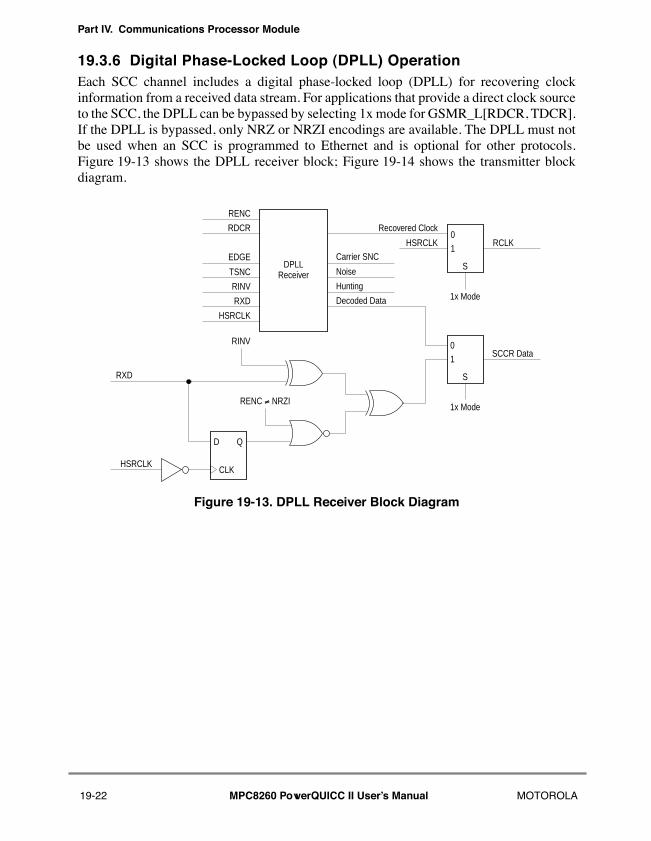
Part IV. Communications Processor Module
19.3.6 Digital Phase-Locked Loop (DPLL) OperationEach SCC channel includes a digital phase-locked loop (DPLL) for recovering clockinformation from a received data stream. For applications that provide a direct clock sourceto the SCC, the DPLL can be bypassed by selecting 1x mode for GSMR_L[RDCR, TDCR].If the DPLL is bypassed, only NRZ or NRZI encodings are available. The DPLL must notbe used when an SCC is programmed to Ethernet and is optional for other protocols.Figure 19-13 shows the DPLL receiver block; Figure 19-14 shows the transmitter blockdiagram.
Figure 19-13. DPLL Receiver Block Diagram
DPLL
HSRCLK
RXD
RINV
TSNC
EDGE
RDCR
RENC
Receiver
Carrier SNC
Decoded Data
Hunting
Noise
0
S
Recovered Clock
HSRCLK RCLK1
1x Mode
0
S
SCCR Data1
1x Mode
D
CLK
Q
HSRCLK
RXD
RINV
RENC ¹ NRZI
19-22 MPC8260 PowerQUICC II UserÕs Manual MOTOROLA
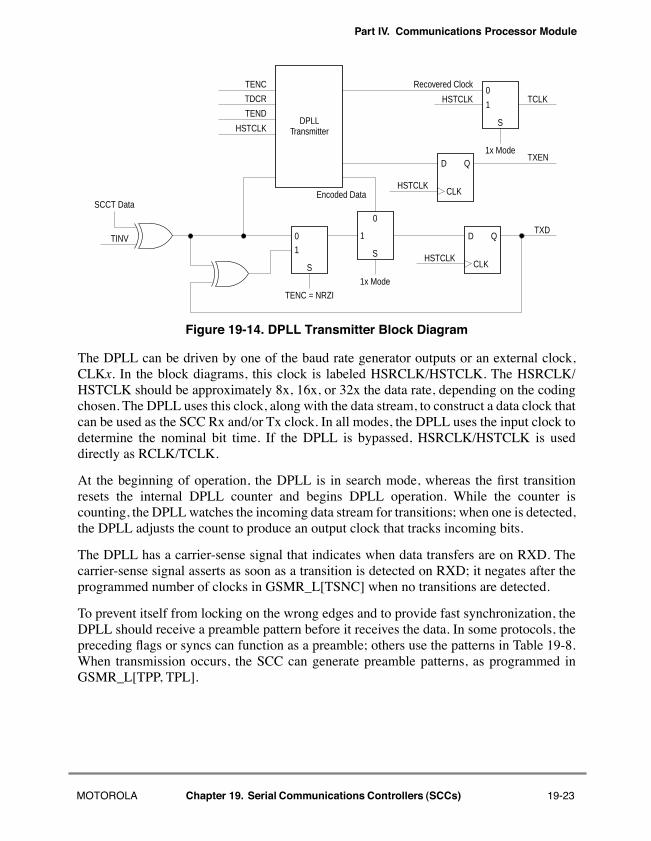
Part IV. Communications Processor Module
Figure 19-14. DPLL Transmitter Block Diagram
The DPLL can be driven by one of the baud rate generator outputs or an external clock,CLKx. In the block diagrams, this clock is labeled HSRCLK/HSTCLK. The HSRCLK/HSTCLK should be approximately 8x, 16x, or 32x the data rate, depending on the codingchosen. The DPLL uses this clock, along with the data stream, to construct a data clock thatcan be used as the SCC Rx and/or Tx clock. In all modes, the DPLL uses the input clock todetermine the nominal bit time. If the DPLL is bypassed, HSRCLK/HSTCLK is useddirectly as RCLK/TCLK.
At the beginning of operation, the DPLL is in search mode, whereas the Þrst transitionresets the internal DPLL counter and begins DPLL operation. While the counter iscounting, the DPLL watches the incoming data stream for transitions; when one is detected,the DPLL adjusts the count to produce an output clock that tracks incoming bits.
The DPLL has a carrier-sense signal that indicates when data transfers are on RXD. Thecarrier-sense signal asserts as soon as a transition is detected on RXD; it negates after theprogrammed number of clocks in GSMR_L[TSNC] when no transitions are detected.
To prevent itself from locking on the wrong edges and to provide fast synchronization, theDPLL should receive a preamble pattern before it receives the data. In some protocols, thepreceding ßags or syncs can function as a preamble; others use the patterns in Table 19-8.When transmission occurs, the SCC can generate preamble patterns, as programmed inGSMR_L[TPP, TPL].
DPLLHSTCLK
TEND
TENC
Transmitter
0
S
Recovered Clock
HSTCLK TCLK1
1x Mode
0
S
1
TENC = NRZI
D
CLK
Q
SCCT Data0
S
1
1x Mode
TDCR
D
CLK
Q
HSTCLK
TXEN
HSTCLK
TXDTINV
Encoded Data
MOTOROLA Chapter 19. Serial Communications Controllers (SCCs) 19-23
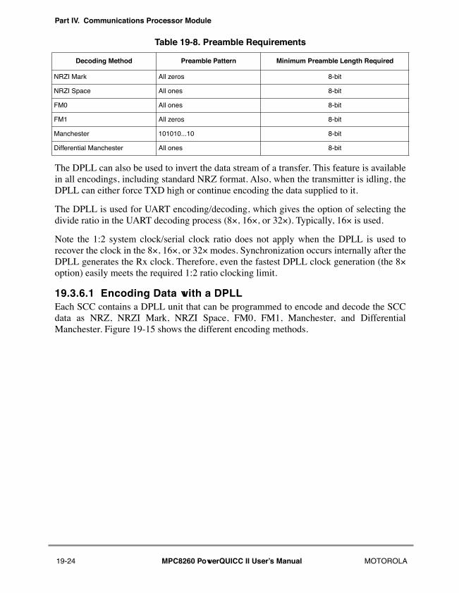
Part IV. Communications Processor Module
The DPLL can also be used to invert the data stream of a transfer. This feature is availablein all encodings, including standard NRZ format. Also, when the transmitter is idling, theDPLL can either force TXD high or continue encoding the data supplied to it.
The DPLL is used for UART encoding/decoding, which gives the option of selecting thedivide ratio in the UART decoding process (8´, 16´, or 32´). Typically, 16´ is used.
Note the 1:2 system clock/serial clock ratio does not apply when the DPLL is used torecover the clock in the 8´, 16´, or 32´ modes. Synchronization occurs internally after theDPLL generates the Rx clock. Therefore, even the fastest DPLL clock generation (the 8´option) easily meets the required 1:2 ratio clocking limit.
19.3.6.1 Encoding Data with a DPLLEach SCC contains a DPLL unit that can be programmed to encode and decode the SCCdata as NRZ, NRZI Mark, NRZI Space, FM0, FM1, Manchester, and DifferentialManchester. Figure 19-15 shows the different encoding methods.
Table 19-8. Preamble Requirements
Decoding Method Preamble Pattern Minimum Preamble Length Required
NRZI Mark All zeros 8-bit
NRZI Space All ones 8-bit
FM0 All ones 8-bit
FM1 All zeros 8-bit
Manchester 101010...10 8-bit
Differential Manchester All ones 8-bit
19-24 MPC8260 PowerQUICC II UserÕs Manual MOTOROLA
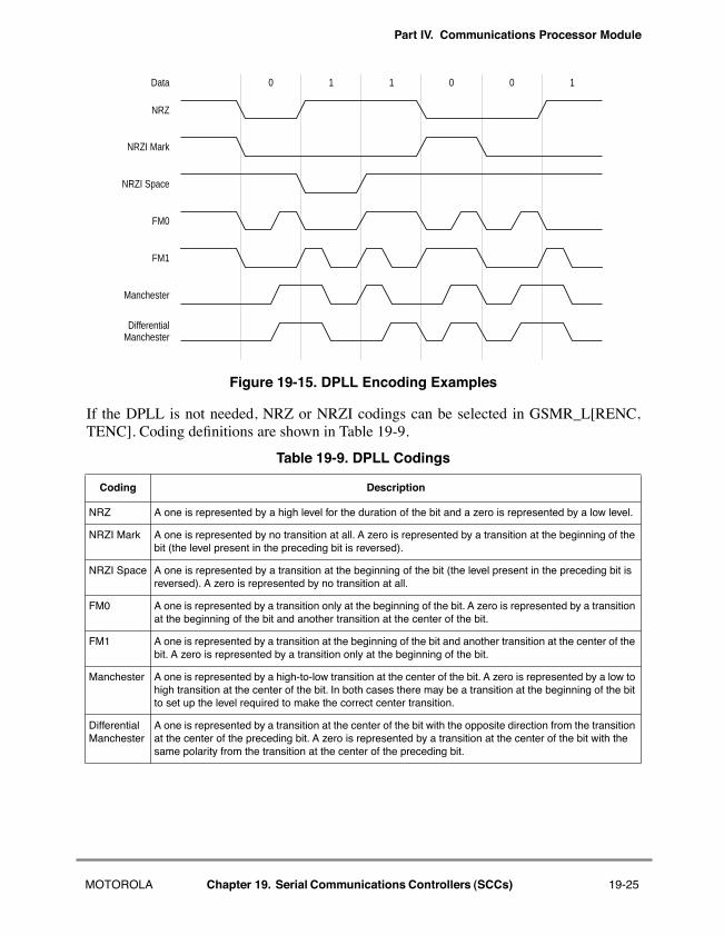
Part IV. Communications Processor Module
Figure 19-15. DPLL Encoding Examples
If the DPLL is not needed, NRZ or NRZI codings can be selected in GSMR_L[RENC,TENC]. Coding deÞnitions are shown in Table 19-9.
Table 19-9. DPLL Codings
Coding Description
NRZ A one is represented by a high level for the duration of the bit and a zero is represented by a low level.
NRZI Mark A one is represented by no transition at all. A zero is represented by a transition at the beginning of the bit (the level present in the preceding bit is reversed).
NRZI Space A one is represented by a transition at the beginning of the bit (the level present in the preceding bit is reversed). A zero is represented by no transition at all.
FM0 A one is represented by a transition only at the beginning of the bit. A zero is represented by a transition at the beginning of the bit and another transition at the center of the bit.
FM1 A one is represented by a transition at the beginning of the bit and another transition at the center of the bit. A zero is represented by a transition only at the beginning of the bit.
Manchester A one is represented by a high-to-low transition at the center of the bit. A zero is represented by a low to high transition at the center of the bit. In both cases there may be a transition at the beginning of the bit to set up the level required to make the correct center transition.
Differential Manchester
A one is represented by a transition at the center of the bit with the opposite direction from the transition at the center of the preceding bit. A zero is represented by a transition at the center of the bit with the same polarity from the transition at the center of the preceding bit.
Data
NRZ
NRZI Mark
NRZI Space
FM0
FM1
Manchester
DifferentialManchester
0 1 1 0 0 1
MOTOROLA Chapter 19. Serial Communications Controllers (SCCs) 19-25
Part IV. Communications Processor Module
19.3.7 Clock Glitch DetectionClock glitches cause problems for many communications systems, and they may goundetected by the system. Systems that supply an external clock to a serial channel are oftensusceptible to glitches from noise, connecting or disconnecting the physical cable from theapplication board, or excessive ringing on a clock line. A clock glitch occurs when morethan one edge occurs in a time period that violates the minimum high or low timespeciÞcation of the input clock.
The SCCs on the MPC8260 have a special circuit designed to detect glitches and alert thesystem of a problem at the physical layer. The glitch-detect circuit is not a speciÞcation test;if a circuit does not meet the SCCÕs input clocking speciÞcations, erroneous data may notbe detected or false glitch indications can occur. Regardless of whether the DPLL is used,the received clock is passed through a noise Þlter that eliminates any noise spikes that affecta single sample. This sampling is enabled using GSMR_H[GDE].
If a spike is detected, a maskable Rx or Tx glitched clock interrupt is generated inSCCEx[GLR,GLT]. Although the receiver or transmitter can be reset or allowed to continueoperation, statistics on clock glitches should be kept for evaluation to help in debugging,especially during prototype testing.
19.3.8 ReconÞguring the SCCsThe proper reconÞguration sequence must be followed for SCC parameters that cannot bechanged dynamically. For instance, the internal baud rate generators allow on-the-ßychanges, but the DPLL-related GSMR does not. The steps in the following sections showhow to disable, reconÞgure and re-enable an SCC to ensure that buffers currently in use areproperly closed before reconÞguring the SCC and that subsequent data goes to or from newbuffers according to the new conÞguration.
Modifying parameter RAM does not require the SCC to be fully disabled. See theparameter RAM description for when values can be changed. To disable all peripheralcontrollers, set CPCR[RST] to reset the entire CPM.
19.3.8.1 General ReconÞguration Sequence for an SCC TransmitterAn SCC transmitter can be reconÞgured by following these general steps:
1. If the SCC is sending data, issue a STOP TRANSMIT command. Transmission should stop smoothly. If the SCC is not transmitting (no TxBDs are ready or the GRACEFUL STOP TRANSMIT command has been issued and completed) or the INIT TX PARAMETERS command is issued, the STOP TRANSMIT command is not required.
2. Clear GSMR_L[ENT] to disable the SCC transmitter and put it in reset state.3. Modify SCC Tx parameters or parameter RAM. To switch protocols or restore the
initial Tx parameters, issue an INIT TX PARAMETERS command.
19-26 MPC8260 PowerQUICC II UserÕs Manual MOTOROLA
Part IV. Communications Processor Module
4. If an INIT TX PARAMETERS command was not issued in step 3, issue a RESTART TRANSMIT command.
5. Set GSMR_L[ENT]. Transmission begins using the TxBD pointed to by TBPTR, assuming the R bit is set.
19.3.8.2 Reset Sequence for an SCC TransmitterThe following steps reinitialize an SCC transmit parameters to the reset state:
1. Clear GSMR_L[ENT].
2. Make any modiÞcations then issue the INIT TX PARAMETERS command.
3. Set GSMR_L[ENT].
19.3.8.3 General ReconÞguration Sequence for an SCC ReceiverAn SCC receiver can be reconÞgured by following these steps:
1. Clear GSMR_L[ENR]. The SCC receiver is now disabled and put in a reset state.
2. Modify SCC Rx parameters or parameter RAM. To switch protocols or restore Rx parameters to their initial state, issue an INIT RX PARAMETERS command.
3. If the INIT RX PARAMETERS command was not issued in step 2, issue an ENTER HUNT MODE command.
4. Set GSMR_L[ENR]. Reception begins using the RxBD pointed to by RBPTR, assuming the E bit is set.
19.3.8.4 Reset Sequence for an SCC ReceiverTo reinitialize the SCC receiver to the state it was in after reset, follow these steps:
1. Clear GSMR_L[ENR].
2. Make any modiÞcations then issue the INIT RX PARAMETERS command.
3. Set GSMR_L[ENR].
19.3.8.5 Switching ProtocolsTo switch an SCCÕs protocol without resetting the board or affecting other SCCs, followthese steps:
1. Clear GSMR_L[ENT, ENR].
2. Make protocol changes in the GSMR and additional parameters then issue the INIT TX and RX PARAMETERS command to initialize both Tx and Rx parameters.
3. Set GSMR_L[ENT, ENR] to enable the SCC with the new protocol.
19.3.9 Saving PowerTo save power when not in use, an SCC can be disabled by clearing GSMR_L[ENT, ENR].
MOTOROLA Chapter 19. Serial Communications Controllers (SCCs) 19-27

Part IV. Communications Processor Module
19-28 MPC8260 PowerQUICC II UserÕs Manual MOTOROLA
Chapter 20 SCC UART Mode200200
The universal asynchronous receiver transmitter (UART) protocol is commonly used tosend low-speed data between devices. The term asynchronous is used because it is notnecessary to send clocking information along with the data being sent. UART links aretypically 38400 baud or less and are character-based. Asynchronous links are used toconnect terminals with other devices. Even where synchronous communications arerequired, the UART is often used as a local port to run board debugger software. Thecharacter format of the UART protocol is shown in Figure 20-1.
Figure 20-1. UART Character Format
Because the transmitter and receiver operate asynchronously, there is no need to connectthe transmit and receive clocks. Instead, the receiver oversamples the incoming data stream(usually by a factor of 16) and uses some of these samples to determine the bit value.Traditionally, the middle 3 of the 16 samples are used. Two UARTs can communicate usingthis system if the transmitter and receiver use the same parameters, such as the parityscheme and character length.
When data is not sent, a continuous stream of ones is sent (idle condition). Because the startbit is always a zero, the receiver can detect when real data is once again on the line. UARTspeciÞes an all-zeros break character, which ends a character transfer sequence.
The most popular protocol that uses asynchronous characters is the RS-232 standard, whichspeciÞes baud rates, handshaking protocols, and mechanical/electrical details. Anotherpopular format is RS-485, which deÞnes a balanced line system allowing longer cables thanRS-232 links. Even synchronous protocols like HDLC are sometimes deÞned to run overasynchronous links. The ProÞbus standard extends UART protocol to include LAN-oriented features such as token passing.
UART TCLK
UART TXD
8x, 16x, or 32x
StartBit
AddrBit
ParityBit
(Optional)
5, 6, 7, or 8 data bits with theleast significant bit first
9/16 to 2stop bits
(Not to scale)
MOTOROLA Chapter 20. SCC UART Mode 20-1
Part IV. Communications Processor Module
All standards provide handshaking signals, but some systems require only three physicallinesÑTx data, Rx data, and ground. Many proprietary standards have been built aroundthe UARTÕs asynchronous character frame, some of which implement a multidropconÞguration where multiple stations, each with a speciÞc address, can be present on anetwork. In multidrop mode, frames of characters are broadcast with the Þrst characteracting as a destination address. To accommodate this, the UART frame is extended one bitto distinguish address characters from normal data characters.
In synchronous UART (isochronous operation), a separate clock signal is explicitlyprovided with the data. Start and stop bits are present in synchronous UART, butoversampling is not required because the clock is provided with each bit.
The general SCC mode register (GSMR) is used to conÞgure an SCC channel to functionin UART mode, which provides standard serial I/O using asynchronous character-based(start-stop) protocols with RS-232C-type lines. Using standard asynchronous bit rates andprotocols, an SCC UART controller can communicate with any existing RS-232-typedevice and provides a serial communications port to other microprocessors and terminals(either locally or via modems). The independent transmit and receive sections, whoseoperations are asynchronous with the core, send data from memory (either internal orexternal) to TXD and receive data from RXD. The UART controller supports a multidropmode for master/slave operations with wake-up capability on both the idle signal andaddress bit. It also supports synchronous operation where a clock (internal or external) mustbe provided with each bit received.
20.1 FeaturesThe following list summarizes main features of an SCC UART controller:
¥ Flexible message-based data structure
¥ Implements synchronous and asynchronous UART
¥ Multidrop operation
¥ Receiver wake-up on idle line or address bit
¥ Receive entire messages into buffers as indicated by receiver idle timeout or by control character reception
¥ Eight control character comparison
¥ Two address comparison in multidrop conÞgurations
¥ Maintenance of four 16-bit error counters
¥ Received break character length indication
¥ Programmable data length (5Ð8 bits)
¥ Programmable fractional stop bit lengths (from 9/16 to 2 bits) in transmission
¥ Capable of reception without a stop bit
¥ Even/odd/force/no parity generation and check
20-2 MPC8260 PowerQUICC II UserÕs Manual MOTOROLA
Part IV. Communications Processor Module
¥ Frame error, noise error, break, and idle detection
¥ Transmit preamble and break sequences
¥ Freeze transmission option with low-latency stop
20.2 Normal Asynchronous ModeIn normal asynchronous mode, the receive shift register receives incoming data on RXDx.Control bits in the UART mode register (PSMR) deÞne the length and format of the UARTcharacter. Bits are received in the following order:
1. Start bit
2. 5Ð8 data bits (lsb Þrst)
3. Address/data bit (optional)
4. Parity bit (optional)
5. Stop bits
The receiver uses a clock 8´, 16´, or 32´ faster than the baud rate and samples each bit ofthe incoming data three times around its center. The value of the bit is determined by themajority of those samples; if all do not agree, the noise indication counter (NOSEC) inparameter RAM is incremented. When a complete character has been clocked in, thecontents of the receive shift register are transferred to the receive FIFO before proceedingto the receive buffer. The CPM ßags UART events, including reception errors, in SCCE andthe RxBD status and control Þelds.
The SCC can receive fractional stop bits. The next characterÕs start bit can begin any timeafter the three middle samples are taken. The UART transmit shift register sends outgoingdata on TXDx. Data is then clocked synchronously with the transmit clock, which may haveeither an internal or external source. Characters are sent lsb Þrst. Only the data portion ofthe UART frame is stored in the buffers because start and stop bits are generated andstripped by the SCC. A parity bit can be generated in transmission and checked duringreception; although it is not stored in the buffer, its value can be inferred from the bufferÕsreporting mechanism. Similarly, the optional address bit is not stored in the transmit orreceive buffer, but is supplied in the BD itself. Parity generation and checking includes theoptional address bit. GSMR_H[RFW] must be set for an 8-bit receive FIFO in the UARTreceiver.
20.3 Synchronous ModeIn synchronous mode, the controller uses a 1´ data clock for timing. The receive shiftregister receives incoming data on RXDx synchronous with the clock. The bit length andformat of the serial character are deÞned by the control bits in the PSMR in the same wayas in asynchronous mode. When a complete byte has been clocked in, the contents of the
MOTOROLA Chapter 20. SCC UART Mode 20-3
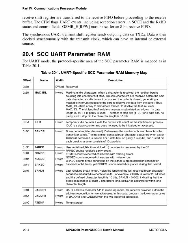
Part IV. Communications Processor Module
receive shift register are transferred to the receive FIFO before proceeding to the receivebuffer. The CPM ßags UART events, including reception errors, in SCCE and the RxBDstatus and control Þelds. GSMR_H[RFW] must be set for an 8-bit receive FIFO.
The synchronous UART transmit shift register sends outgoing data on TXDx. Data is thenclocked synchronously with the transmit clock, which can have an internal or externalsource.
20.4 SCC UART Parameter RAM For UART mode, the protocol-speciÞc area of the SCC parameter RAM is mapped as inTable 20-1.
Table 20-1. UART-Specific SCC Parameter RAM Memory Map
Offset 1 Name Width Description
0x30 Ñ DWord Reserved
0x38 MAX_IDL Hword Maximum idle characters. When a character is received, the receiver begins counting idle characters. If MAX_IDL idle characters are received before the next data character, an idle timeout occurs and the buffer is closed, generating a maskable interrupt request to the core to receive the data from the buffer. Thus, MAX_IDL offers a way to demarcate frames. To disable the feature, clear MAX_IDL. The bit length of an idle character is calculated as follows: 1 + data length (5Ð9) + 1 (if parity is used) + number of stop bits (1Ð2). For 8 data bits, no parity, and 1 stop bit, the character length is 10 bits.
0x3A IDLC Hword Temporary idle counter. Holds the current idle count for the idle timeout process. IDLC is a down-counter and does not need to be initialized or accessed.
0x3C BRKCR Hword Break count register (transmit). Determines the number of break characters the transmitter sends. The transmitter sends a break character sequence when a STOP TRANSMIT command is issued. For 8 data bits, no parity, 1 stop bit, and 1 start bit, each break character consists of 10 zero bits.
0x3E PAREC Hword User-initialized,16-bit (moduloÐ216
) counters incremented by the CP.PAREC counts received parity errors. FRMEC counts received characters with framing errors. NOSEC counts received characters with noise errors. BRKEC counts break conditions on the signal. A break condition can last for hundreds of bit times, yet BRKEC is incremented only once during that period.
0x40 FRMEC Hword
0x42 NOSEC Hword
0x44 BRKEC Hword
0x46 BRKLN Hword Last received break length. Holds the length of the last received break character sequence measured in character units. For example, if RXDx is low for 20 bit times and the deÞned character length is 10 bits, BRKLN = 0x002, indicating that the break sequence is at least 2 characters long. BRKLN is accurate to within one character length.
0x48 UADDR1 Hword UART address character 1/2. In multidrop mode, the receiver provides automatic address recognition for two addresses. In this case, program the lower order bytes of UADDR1 and UADDR2 with the two preferred addresses.0x4A UADDR2 Hword
0x4C RTEMP Hword Temp storage
20-4 MPC8260 PowerQUICC II UserÕs Manual MOTOROLA
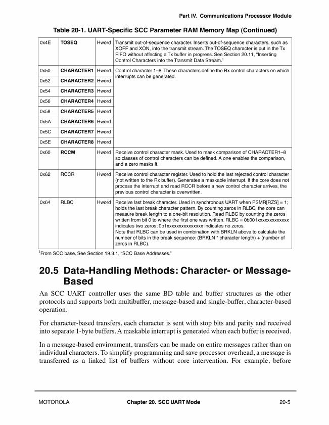
Part IV. Communications Processor Module
20.5 Data-Handling Methods: Character- or Message-Based
An SCC UART controller uses the same BD table and buffer structures as the otherprotocols and supports both multibuffer, message-based and single-buffer, character-basedoperation.
For character-based transfers, each character is sent with stop bits and parity and receivedinto separate 1-byte buffers. A maskable interrupt is generated when each buffer is received.
In a message-based environment, transfers can be made on entire messages rather than onindividual characters. To simplify programming and save processor overhead, a message istransferred as a linked list of buffers without core intervention. For example, before
0x4E TOSEQ Hword Transmit out-of-sequence character. Inserts out-of-sequence characters, such as XOFF and XON, into the transmit stream. The TOSEQ character is put in the Tx FIFO without affecting a Tx buffer in progress. See Section 20.11, ÒInserting Control Characters into the Transmit Data Stream.Ó
0x50 CHARACTER1 Hword Control character 1Ð8. These characters deÞne the Rx control characters on which interrupts can be generated.
0x52 CHARACTER2 Hword
0x54 CHARACTER3 Hword
0x56 CHARACTER4 Hword
0x58 CHARACTER5 Hword
0x5A CHARACTER6 Hword
0x5C CHARACTER7 Hword
0x5E CHARACTER8 Hword
0x60 RCCM Hword Receive control character mask. Used to mask comparison of CHARACTER1Ð8 so classes of control characters can be deÞned. A one enables the comparison, and a zero masks it.
0x62 RCCR Hword Receive control character register. Used to hold the last rejected control character (not written to the Rx buffer). Generates a maskable interrupt. If the core does not process the interrupt and read RCCR before a new control character arrives, the previous control character is overwritten.
0x64 RLBC Hword Receive last break character. Used in synchronous UART when PSMR[RZS] = 1; holds the last break character pattern. By counting zeros in RLBC, the core can measure break length to a one-bit resolution. Read RLBC by counting the zeros written from bit 0 to where the Þrst one was written. RLBC = 0b001xxxxxxxxxxxxx indicates two zeros; 0b1xxxxxxxxxxxxxxx indicates no zeros.Note that RLBC can be used in combination with BRKLN above to calculate the number of bits in the break sequence: (BRKLN * character length) + (number of zeros in RLBC).
1From SCC base. See Section 19.3.1, ÒSCC Base Addresses.Ó
Table 20-1. UART-Specific SCC Parameter RAM Memory Map (Continued)
MOTOROLA Chapter 20. SCC UART Mode 20-5
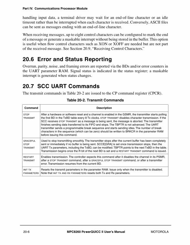
Part IV. Communications Processor Module
handling input data, a terminal driver may wait for an end-of-line character or an idletimeout rather than be interrupted when each character is received. Conversely, ASCII Þlescan be sent as messages ending with an end-of-line character.
When receiving messages, up to eight control characters can be conÞgured to mark the endof a message or generate a maskable interrupt without being stored in the buffer. This optionis useful when ßow control characters such as XON or XOFF are needed but are not partof the received message. See Section 20.9, ÒReceiving Control Characters.Ó
20.6 Error and Status ReportingOverrun, parity, noise, and framing errors are reported via the BDs and/or error counters inthe UART parameter RAM. Signal status is indicated in the status register; a maskableinterrupt is generated when status changes.
20.7 SCC UART CommandsThe transmit commands in Table 20-2 are issued to the CP command register (CPCR).
Table 20-2. Transmit Commands
Command Description
STOP TRANSMIT
After a hardware or software reset and a channel is enabled in the GSMR, the transmitter starts polling the Þrst BD in the TxBD table every 8 Tx clocks. STOP TRANSMIT disables character transmission. If the SCC receives STOP TRANSMIT as a message is being sent, the message is aborted. The transmitter Þnishes sending data transferred to its FIFO and stops. The TBPTR is not advanced. The UART transmitter sends a programmable break sequence and starts sending idles. The number of break characters in the sequence (which can be zero) should be written to BRKCR in the parameter RAM before issuing this command.
GRACEFUL STOP TRANSMIT
Used to stop transmitting smoothly. The transmitter stops after the current buffer has been completely sent or immediately if no buffer is being sent. SCCE[GRA] is set once transmission stops, then the UART Tx parameters, including the TxBD, can be modiÞed. TBPTR points to the next TxBD in the table. Transmission begins once the R bit of the next BD is set and a RESTART TRANSMIT command is issued.
RESTART TRANSMIT
Enables transmission. The controller expects this command after it disables the channel in its PSMR, after a STOP TRANSMIT command, after a GRACEFUL STOP TRANSMIT command, or after a transmitter error. Transmission resumes from the current BD.
INIT TX PARAMETERS
Resets the transmit parameters in the parameter RAM. Issue only when the transmitter is disabled. Note that INIT TX AND RX PARAMETERS resets both Tx and Rx parameters.
20-6 MPC8260 PowerQUICC II UserÕs Manual MOTOROLA
Part IV. Communications Processor Module
Receive commands are described in Table 20-3.
20.8 Multidrop Systems and Address RecognitionIn multidrop systems, more than two stations can be on a network, each with a speciÞcaddress. Figure 20-2 shows two examples of this conÞguration. Frames made up of manycharacters can be broadcast as long as the Þrst character is the destination address. TheUART frame is extended by one bit to distinguish an address character from standard datacharacters. Programmed in PSMR[UM], the controller supports the following twomultidrop modes:
¥ Automatic multidrop modeÑThe controller checks the incoming address character and accepts subsequent data only if the address matches one of two user-deÞned values. The two 16-bit address registers, UADDR1 and UADDR2, support address recognition. Only the lower 8 bits are used so the upper 8 bits should be cleared; for addresses less than 8 bits, unused high-order bits should also be cleared. The incoming address is checked against UADDR1 and UADDR2. When a match occurs, RxBD[AM] indicates whether UADDR1 or UADDR2 matched.
¥ Manual multidrop modeÑThe controller receives all characters. An address character is always written to a new buffer and can be followed by data characters. User software performs the address comparison.
Table 20-3. Receive Commands
Command Description
ENTER HUNT MODE
Forces the receiver to close the RxBD in use and enter hunt mode. After a hardware or software reset, once an SCC is enabled in the GSMR, the receiver is automatically enabled and uses the Þrst BD in the RxBD table. If a message is in progress, the receiver continues receiving in the next BD. In multidrop hunt mode, the receiver continually scans the input data stream for the address character. When it is not in multidrop mode, it waits for the idle sequence (one character of idle). Data present in the Rx FIFO is not lost when this command is executed.
CLOSE RXBD Forces the SCC to close the RxBD in use and use the next BD for subsequent received data. If the SCC is not in the process of receiving data, no action is taken.Note that in an SCC UART controller, CLOSE RXBD functions like ENTER HUNT MODE but does not need to receive an idle character to continue receiving.
INIT RX PARAMETERS
Resets the receive parameters in the parameter RAM. Should be issued when the receiver is disabled. Note that INIT TX AND RX PARAMETERS resets both Tx and Rx parameters.
MOTOROLA Chapter 20. SCC UART Mode 20-7
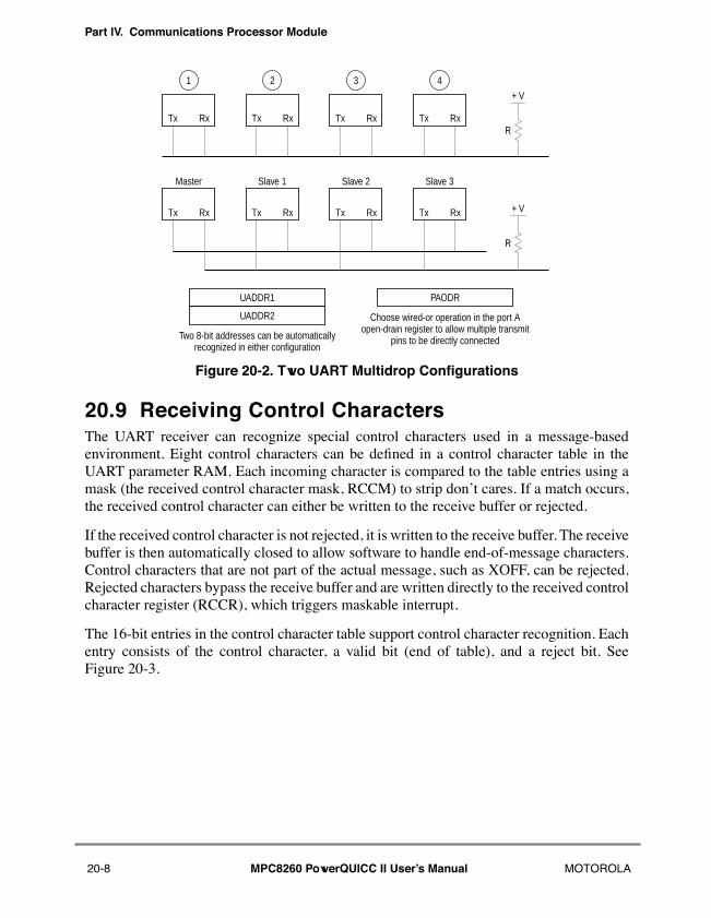
Part IV. Communications Processor Module
Figure 20-2. Two UART Multidrop Configurations
20.9 Receiving Control CharactersThe UART receiver can recognize special control characters used in a message-basedenvironment. Eight control characters can be deÞned in a control character table in theUART parameter RAM. Each incoming character is compared to the table entries using amask (the received control character mask, RCCM) to strip donÕt cares. If a match occurs,the received control character can either be written to the receive buffer or rejected.
If the received control character is not rejected, it is written to the receive buffer. The receivebuffer is then automatically closed to allow software to handle end-of-message characters.Control characters that are not part of the actual message, such as XOFF, can be rejected.Rejected characters bypass the receive buffer and are written directly to the received controlcharacter register (RCCR), which triggers maskable interrupt.
The 16-bit entries in the control character table support control character recognition. Eachentry consists of the control character, a valid bit (end of table), and a reject bit. SeeFigure 20-3.
Tx Rx
1
Tx Rx
2
Tx Rx
3
Tx Rx
4
Tx Rx Tx Rx Tx Rx Tx Rx
Slave 2 Slave 3Slave 1Master
UADDR1
UADDR2
PAODR
Choose wired-or operation in the port Aopen-drain register to allow multiple transmit
pins to be directly connected
+ V
R
Two 8-bit addresses can be automaticallyrecognized in either configuration
+ V
R
20-8 MPC8260 PowerQUICC II UserÕs Manual MOTOROLA
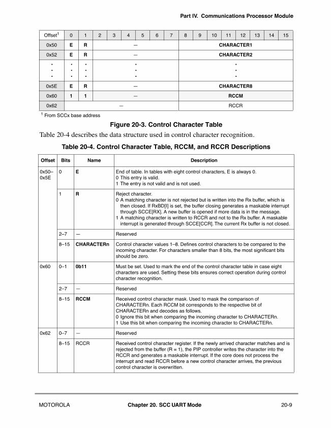
Part IV. Communications Processor Module
Table 20-4 describes the data structure used in control character recognition.
Offset1 0 1 2 3 4 5 6 7 8 9 10 11 12 13 14 15
0x50 E R Ñ CHARACTER1
0x52 E R Ñ CHARACTER2
¥¥¥
¥¥¥
¥¥¥
¥¥¥
¥¥¥
0x5E E R Ñ CHARACTER8
0x60 1 1 Ñ RCCM
0x62 Ñ RCCR
1 From SCCx base address
Figure 20-3. Control Character Table
Table 20-4. Control Character Table, RCCM, and RCCR Descriptions
Offset Bits Name Description
0x50Ð0x5E
0 E End of table. In tables with eight control characters, E is always 0.0 This entry is valid.1 The entry is not valid and is not used.
1 R Reject character.0 A matching character is not rejected but is written into the Rx buffer, which is
then closed. If RxBD[I] is set, the buffer closing generates a maskable interrupt through SCCE[RX]. A new buffer is opened if more data is in the message.
1 A matching character is written to RCCR and not to the Rx buffer. A maskable interrupt is generated through SCCE[CCR]. The current Rx buffer is not closed.
2Ð7 Ñ Reserved
8Ð15 CHARACTERn Control character values 1Ð8. DeÞnes control characters to be compared to the incoming character. For characters smaller than 8 bits, the most signiÞcant bits should be zero.
0x60 0Ð1 0b11 Must be set. Used to mark the end of the control character table in case eight characters are used. Setting these bits ensures correct operation during control character recognition.
2Ð7 Ñ Reserved
8Ð15 RCCM Received control character mask. Used to mask the comparison of CHARACTERn. Each RCCM bit corresponds to the respective bit of CHARACTERn and decodes as follows. 0 Ignore this bit when comparing the incoming character to CHARACTERn.1 Use this bit when comparing the incoming character to CHARACTERn.
0x62 0Ð7 Ñ Reserved
8Ð15 RCCR Received control character register. If the newly arrived character matches and is rejected from the buffer (R = 1), the PIP controller writes the character into the RCCR and generates a maskable interrupt. If the core does not process the interrupt and read RCCR before a new control character arrives, the previous control character is overwritten.
MOTOROLA Chapter 20. SCC UART Mode 20-9
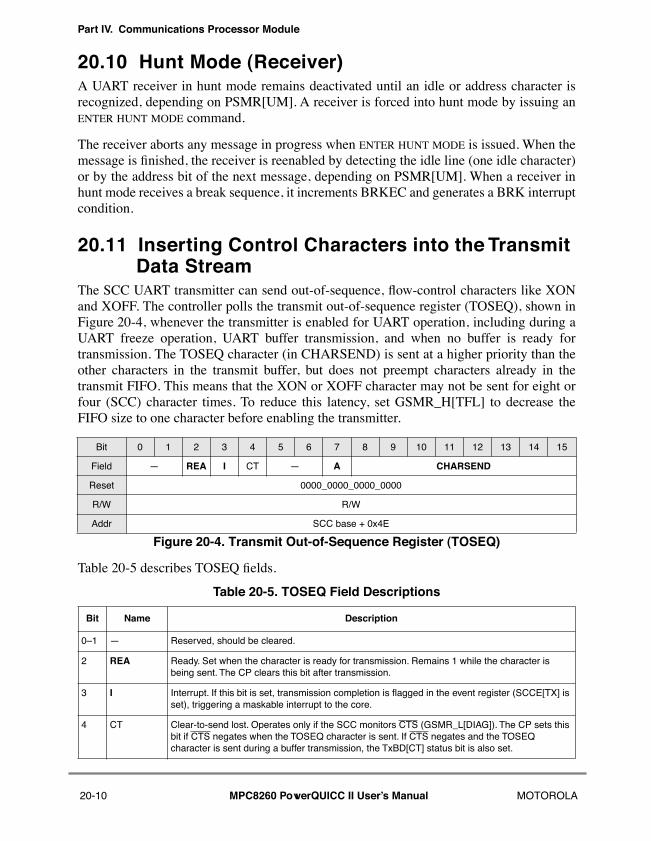
Part IV. Communications Processor Module
20.10 Hunt Mode (Receiver)A UART receiver in hunt mode remains deactivated until an idle or address character isrecognized, depending on PSMR[UM]. A receiver is forced into hunt mode by issuing anENTER HUNT MODE command.
The receiver aborts any message in progress when ENTER HUNT MODE is issued. When themessage is Þnished, the receiver is reenabled by detecting the idle line (one idle character)or by the address bit of the next message, depending on PSMR[UM]. When a receiver inhunt mode receives a break sequence, it increments BRKEC and generates a BRK interruptcondition.
20.11 Inserting Control Characters into the Transmit Data Stream
The SCC UART transmitter can send out-of-sequence, ßow-control characters like XONand XOFF. The controller polls the transmit out-of-sequence register (TOSEQ), shown inFigure 20-4, whenever the transmitter is enabled for UART operation, including during aUART freeze operation, UART buffer transmission, and when no buffer is ready fortransmission. The TOSEQ character (in CHARSEND) is sent at a higher priority than theother characters in the transmit buffer, but does not preempt characters already in thetransmit FIFO. This means that the XON or XOFF character may not be sent for eight orfour (SCC) character times. To reduce this latency, set GSMR_H[TFL] to decrease theFIFO size to one character before enabling the transmitter.
Table 20-5 describes TOSEQ Þelds.
Bit 0 1 2 3 4 5 6 7 8 9 10 11 12 13 14 15
Field Ñ REA I CT Ñ A CHARSEND
Reset 0000_0000_0000_0000
R/W R/W
Addr SCC base + 0x4E
Figure 20-4. Transmit Out-of-Sequence Register (TOSEQ)
Table 20-5. TOSEQ Field Descriptions
Bit Name Description
0Ð1 Ñ Reserved, should be cleared.
2 REA Ready. Set when the character is ready for transmission. Remains 1 while the character is being sent. The CP clears this bit after transmission.
3 I Interrupt. If this bit is set, transmission completion is ßagged in the event register (SCCE[TX] is set), triggering a maskable interrupt to the core.
4 CT Clear-to-send lost. Operates only if the SCC monitors CTS (GSMR_L[DIAG]). The CP sets this bit if CTS negates when the TOSEQ character is sent. If CTS negates and the TOSEQ character is sent during a buffer transmission, the TxBD[CT] status bit is also set.
20-10 MPC8260 PowerQUICC II UserÕs Manual MOTOROLA
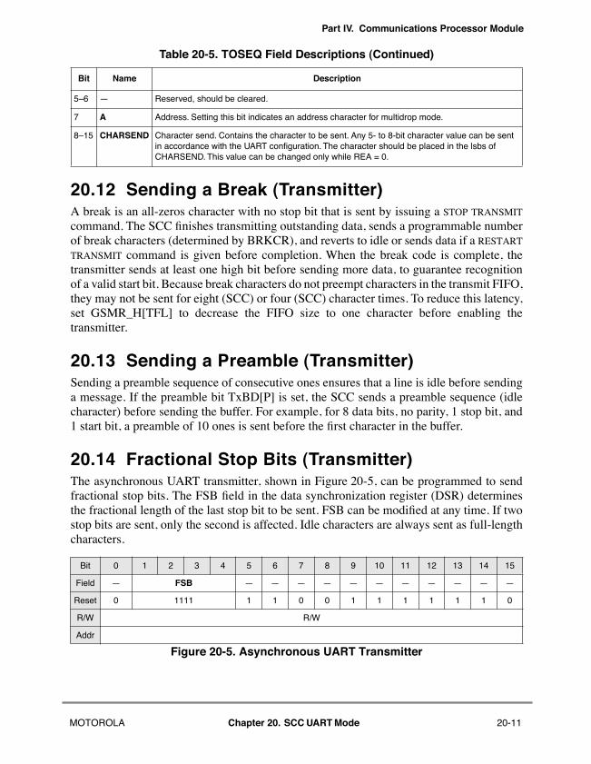
Part IV. Communications Processor Module
20.12 Sending a Break (Transmitter)A break is an all-zeros character with no stop bit that is sent by issuing a STOP TRANSMIT
command. The SCC Þnishes transmitting outstanding data, sends a programmable numberof break characters (determined by BRKCR), and reverts to idle or sends data if a RESTART
TRANSMIT command is given before completion. When the break code is complete, thetransmitter sends at least one high bit before sending more data, to guarantee recognitionof a valid start bit. Because break characters do not preempt characters in the transmit FIFO,they may not be sent for eight (SCC) or four (SCC) character times. To reduce this latency,set GSMR_H[TFL] to decrease the FIFO size to one character before enabling thetransmitter.
20.13 Sending a Preamble (Transmitter)Sending a preamble sequence of consecutive ones ensures that a line is idle before sendinga message. If the preamble bit TxBD[P] is set, the SCC sends a preamble sequence (idlecharacter) before sending the buffer. For example, for 8 data bits, no parity, 1 stop bit, and1 start bit, a preamble of 10 ones is sent before the Þrst character in the buffer.
20.14 Fractional Stop Bits (Transmitter)The asynchronous UART transmitter, shown in Figure 20-5, can be programmed to sendfractional stop bits. The FSB Þeld in the data synchronization register (DSR) determinesthe fractional length of the last stop bit to be sent. FSB can be modiÞed at any time. If twostop bits are sent, only the second is affected. Idle characters are always sent as full-lengthcharacters.
5Ð6 Ñ Reserved, should be cleared.
7 A Address. Setting this bit indicates an address character for multidrop mode.
8Ð15 CHARSEND Character send. Contains the character to be sent. Any 5- to 8-bit character value can be sent in accordance with the UART conÞguration. The character should be placed in the lsbs of CHARSEND. This value can be changed only while REA = 0.
Bit 0 1 2 3 4 5 6 7 8 9 10 11 12 13 14 15
Field Ñ FSB Ñ Ñ Ñ Ñ Ñ Ñ Ñ Ñ Ñ Ñ Ñ
Reset 0 1111 1 1 0 0 1 1 1 1 1 1 0
R/W R/W
Addr
Figure 20-5. Asynchronous UART Transmitter
Table 20-5. TOSEQ Field Descriptions (Continued)
Bit Name Description
MOTOROLA Chapter 20. SCC UART Mode 20-11
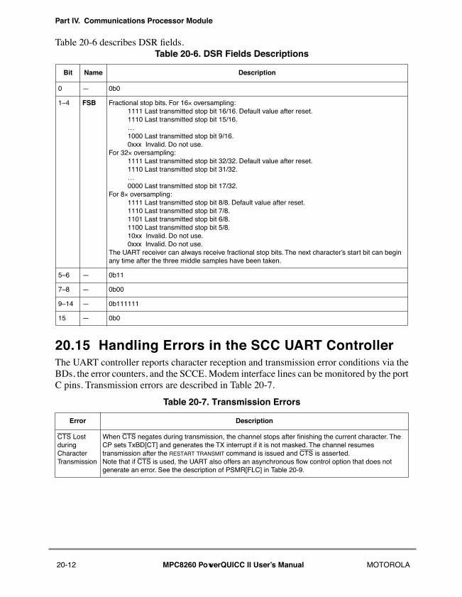
Part IV. Communications Processor Module
Table 20-6 describes DSR Þelds.
20.15 Handling Errors in the SCC UART ControllerThe UART controller reports character reception and transmission error conditions via theBDs, the error counters, and the SCCE. Modem interface lines can be monitored by the portC pins. Transmission errors are described in Table 20-7.
Table 20-6. DSR Fields Descriptions
Bit Name Description
0 Ñ 0b0
1Ð4 FSB Fractional stop bits. For 16´ oversampling:1111 Last transmitted stop bit 16/16. Default value after reset.1110 Last transmitted stop bit 15/16.É1000 Last transmitted stop bit 9/16.0xxx Invalid. Do not use.
For 32´ oversampling:1111 Last transmitted stop bit 32/32. Default value after reset.1110 Last transmitted stop bit 31/32.É0000 Last transmitted stop bit 17/32.
For 8´ oversampling:1111 Last transmitted stop bit 8/8. Default value after reset.1110 Last transmitted stop bit 7/8.1101 Last transmitted stop bit 6/8.1100 Last transmitted stop bit 5/8.10xx Invalid. Do not use.0xxx Invalid. Do not use.
The UART receiver can always receive fractional stop bits. The next characterÕs start bit can begin any time after the three middle samples have been taken.
5Ð6 Ñ 0b11
7Ð8 Ñ 0b00
9Ð14 Ñ 0b111111
15 Ñ 0b0
Table 20-7. Transmission Errors
Error Description
CTS Lost during Character Transmission
When CTS negates during transmission, the channel stops after Þnishing the current character. The CP sets TxBD[CT] and generates the TX interrupt if it is not masked. The channel resumes transmission after the RESTART TRANSMIT command is issued and CTS is asserted. Note that if CTS is used, the UART also offers an asynchronous ßow control option that does not generate an error. See the description of PSMR[FLC] in Table 20-9.
20-12 MPC8260 PowerQUICC II UserÕs Manual MOTOROLA
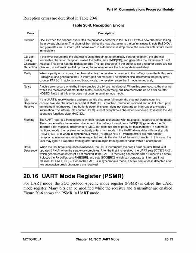
Part IV. Communications Processor Module
Reception errors are described in Table 20-8.
20.16 UART Mode Register (PSMR)For UART mode, the SCC protocol-speciÞc mode register (PSMR) is called the UARTmode register. Many bits can be modiÞed while the receiver and transmitter are enabled.Figure 20-6 shows the PSMR in UART mode.
Table 20-8. Reception Errors
Error Description
Overrun Occurs when the channel overwrites the previous character in the Rx FIFO with a new character, losing the previous character. The channel then writes the new character to the buffer, closes it, sets RxBD[OV], and generates an RX interrupt if not masked. In automatic multidrop mode, the receiver enters hunt mode immediately.
CD Lost during Character Reception
If this error occurs and the channel is using this pin to automatically control reception, the channel terminates character reception, closes the buffer, sets RxBD[CD], and generates the RX interrupt if not masked. This error has the highest priority. The last character in the buffer is lost and other errors are not checked. In automatic multidrop mode, the receiver enters the hunt mode immediately.
Parity When a parity error occurs, the channel writes the received character to the buffer, closes the buffer, sets RxBD[PR], and generates the RX interrupt if not masked. The channel also increments the parity error counter PAREC. In automatic multidrop mode, the receiver enters hunt mode immediately.
Noise A noise error occurs when the three samples of a bit are not identical. When this error occurs, the channel writes the received character to the buffer, proceeds normally, but increments the noise error counter NOSEC. Note that this error does not occur in synchronous mode.
Idle Sequence Receive
If the UART is receiving data and gets an idle character (all ones), the channel begins counting consecutive idle characters received. If MAX_IDL is reached, the buffer is closed and an RX interrupt is generated if not masked. If no buffer is open, this event does not generate an interrupt or any status information. The internal idle counter (IDLC) is reset every time a character is received. To disable the idle sequence function, clear MAX_IDL.
Framing The UART reports a framing errors when it receives a character with no stop bit, regardless of the mode. The channel writes the received character to the buffer, closes it, sets RxBD[FR], generates the RX interrupt if not masked, increments FRMEC, but does not check parity for this character. In automatic multidrop mode, the receiver immediately enters hunt mode. If the UART allows data with no stop bits (PSMR[RZS] = 1) when in synchronous mode (PSMR[SYN] = 1), framing errors are reported but reception continues assuming the unexpected zero is the start bit of the next character; in this case, the user may ignore a reported framing error until multiple framing errors occur within a short period.
Break Sequence
When the Þrst break sequence is received, the UART increments the break error counter BRKEC. It updates BRKLN when the sequence completes. After the Þrst 1 is received, the UART sets SCCE[BRKE], which generates an interrupt if not masked. If the UART is receiving characters when it receives a break, it closes the Rx buffer, sets RxBD[BR], and sets SCCE[RX], which can generate an interrupt if not masked. If PSMR[RZS] = 1 when the UART is in synchronous mode, a break sequence is detected after two successive break characters are received.
MOTOROLA Chapter 20. SCC UART Mode 20-13
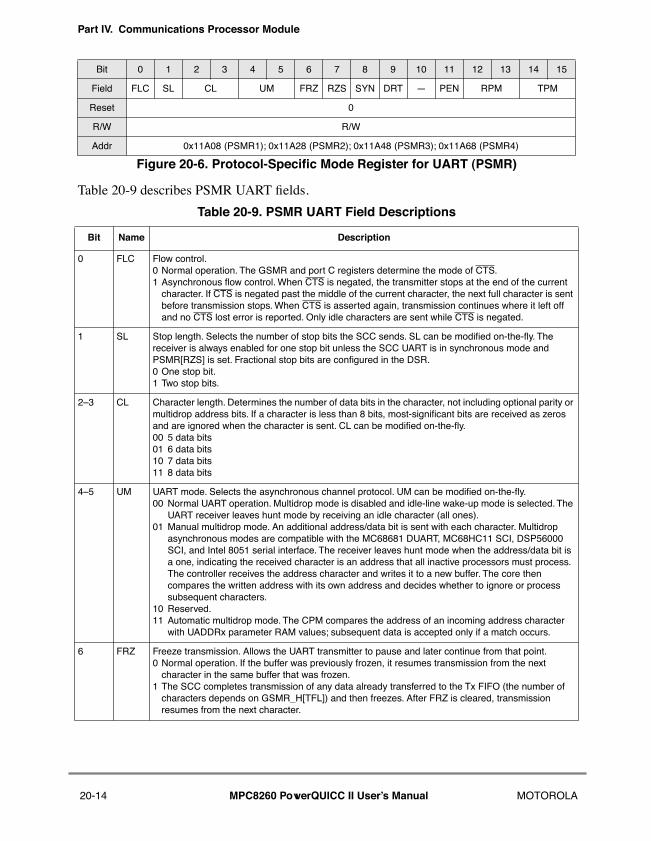
Part IV. Communications Processor Module
Table 20-9 describes PSMR UART Þelds.
Bit 0 1 2 3 4 5 6 7 8 9 10 11 12 13 14 15
Field FLC SL CL UM FRZ RZS SYN DRT Ñ PEN RPM TPM
Reset 0
R/W R/W
Addr 0x11A08 (PSMR1); 0x11A28 (PSMR2); 0x11A48 (PSMR3); 0x11A68 (PSMR4)
Figure 20-6. Protocol-Specific Mode Register for UART (PSMR)
Table 20-9. PSMR UART Field Descriptions
Bit Name Description
0 FLC Flow control. 0 Normal operation. The GSMR and port C registers determine the mode of CTS.1 Asynchronous ßow control. When CTS is negated, the transmitter stops at the end of the current
character. If CTS is negated past the middle of the current character, the next full character is sent before transmission stops. When CTS is asserted again, transmission continues where it left off and no CTS lost error is reported. Only idle characters are sent while CTS is negated.
1 SL Stop length. Selects the number of stop bits the SCC sends. SL can be modiÞed on-the-ßy. The receiver is always enabled for one stop bit unless the SCC UART is in synchronous mode and PSMR[RZS] is set. Fractional stop bits are conÞgured in the DSR.0 One stop bit.1 Two stop bits.
2Ð3 CL Character length. Determines the number of data bits in the character, not including optional parity or multidrop address bits. If a character is less than 8 bits, most-signiÞcant bits are received as zeros and are ignored when the character is sent. CL can be modiÞed on-the-ßy.00 5 data bits01 6 data bits10 7 data bits11 8 data bits
4Ð5 UM UART mode. Selects the asynchronous channel protocol. UM can be modiÞed on-the-ßy.00 Normal UART operation. Multidrop mode is disabled and idle-line wake-up mode is selected. The
UART receiver leaves hunt mode by receiving an idle character (all ones).01 Manual multidrop mode. An additional address/data bit is sent with each character. Multidrop
asynchronous modes are compatible with the MC68681 DUART, MC68HC11 SCI, DSP56000 SCI, and Intel 8051 serial interface. The receiver leaves hunt mode when the address/data bit is a one, indicating the received character is an address that all inactive processors must process. The controller receives the address character and writes it to a new buffer. The core then compares the written address with its own address and decides whether to ignore or process subsequent characters.
10 Reserved.11 Automatic multidrop mode. The CPM compares the address of an incoming address character
with UADDRx parameter RAM values; subsequent data is accepted only if a match occurs.
6 FRZ Freeze transmission. Allows the UART transmitter to pause and later continue from that point.0 Normal operation. If the buffer was previously frozen, it resumes transmission from the next
character in the same buffer that was frozen.1 The SCC completes transmission of any data already transferred to the Tx FIFO (the number of
characters depends on GSMR_H[TFL]) and then freezes. After FRZ is cleared, transmission resumes from the next character.
20-14 MPC8260 PowerQUICC II UserÕs Manual MOTOROLA
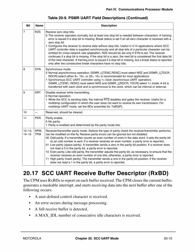
Part IV. Communications Processor Module
20.17 SCC UART Receive Buffer Descriptor (RxBD)The CPM uses RxBDs to report on each buffer received. The CPM closes the current buffer,generates a maskable interrupt, and starts receiving data into the next buffer after one of thefollowing occurs:
¥ A user-deÞned control character is received.
¥ An error occurs during message processing.
¥ A full receive buffer is detected.
¥ A MAX_IDL number of consecutive idle characters is received.
7 RZS Receive zero stop bits. 0 The receiver operates normally, but at least one stop bit is needed between characters. A framing
error is issued if a stop bit is missing. Break status is set if an all-zero character is received with a zero stop bit.
1 ConÞgures the receiver to receive data without stop bits. Useful in V.14 applications where SCC UART controller data is supplied synchronously and all stop bits of a particular character can be omitted for cross-network rate adaptation. RZS should be set only if SYN is set. The receiver continues if a stop bit is missing. If the stop bit is a zero, the next bit is considered the Þrst data bit of the next character. A framing error is issued if a stop bit is missing, but a break status is reported only after two consecutive break characters have no stop bits.
8 SYN Synchronous mode. 0 Normal asynchronous operation. GSMR_L[TENC,RENC] must select NRZ and GSMR_L[TDCR,
RDCR] select either 8´, 16´, or 32´. 16´ is recommended for most applications.1 Synchronous SCC UART controller using 1´ clock (isochronous UART operation).
GSMR_L[TENC, RENC] must select NRZ and GSMR_L[RDCR, TDCR] select 1´ mode. A bit is transferred with each clock and is synchronous to the clock, which can be internal or external.
9 DRT Disable receiver while transmitting.0 Normal operation.1 While the SCC is sending data, the internal RTS disables and gates the receiver. Useful for a
multidrop conÞguration in which the user does not want to receive its own transmission. For multidrop UART mode, set the BDsÕ preamble bit, TxBD[P].
10 Ñ Reserved, should be cleared.
11 PEN Parity enable. 0 No parity.1 Parity is enabled and determined by the parity mode bits.
12Ð13, 14Ð15
RPM, TPM
Receiver/transmitter parity mode. Selects the type of parity check the receiver/transmitter performs; can be modiÞed on-the-ßy. Receive parity errors can be ignored but not disabled.00 Odd parity. If a transmitter counts an even number of ones in the data word, it sets the parity bit
so an odd number is sent. If a receiver receives an even number, a parity error is reported. 01 Low parity (space parity). A transmitter sends a zero in the parity bit position. If a receiver does
not read a 0 in the parity bit, a parity error is reported. 10 Even parity. Like odd parity, the transmitter adjusts the parity bit, as necessary, to ensure that the
receiver receives an even number of one bits; otherwise, a parity error is reported.11 High parity (mark parity). The transmitter sends a one in the parity bit position. If the receiver
does not read a 1 in the parity bit, a parity error is reported.
Table 20-9. PSMR UART Field Descriptions (Continued)
Bit Name Description
MOTOROLA Chapter 20. SCC UART Mode 20-15
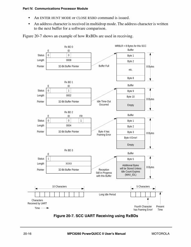
Part IV. Communications Processor Module
¥ An ENTER HUNT MODE or CLOSE RXBD command is issued.
¥ An address character is received in multidrop mode. The address character is written to the next buffer for a software comparison.
Figure 20-7 shows an example of how RxBDs are used in receiving.
Figure 20-7. SCC UART Receiving using RxBDs
Byte 5
Buffer
0
0008
32-Bit Buffer Pointer
0
E IDRx BD 0
Status
Length
Pointer
0
0002
32-Bit Buffer Pointer
1
E IDRx BD 1
Status
Length
Pointer
0
0004
32-Bit Buffer Pointer
0
E IDRx BD 2
Status
Length
Pointer
1
XXXX
32-Bit Buffer Pointer
ERx BD 3
Status
Length
Pointer
Byte 1
Byte 2
Byte 8
Buffer
Byte 9
Byte 10
Buffer
Byte 1
Byte 2
Byte 3
Buffer
Byte 4 Error!
Empty
Additional Byteswill be Stored Unless
Idle Count Expires(MAX_IDL)
8 Bytes
8 Bytes
8 Bytes
8 Bytes
CharactersReceived by UART
Fourth Character
10 Characters
Long Idle Period
has Framing Error!Present
TimeTime
5 Characters
Buffer Full
Idle Time-OutOccurred
Byte 4 hasFraming Error
ReceptionStill in Progresswith this Buffer
1
FR
etc.
Empty
MRBLR = 8 Bytes for this SCC
20-16 MPC8260 PowerQUICC II UserÕs Manual MOTOROLA
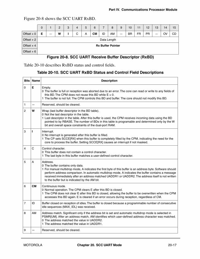
Part IV. Communications Processor Module
Figure 20-8 shows the SCC UART RxBD.
Table 20-10 describes RxBD status and control Þelds.
0 1 2 3 4 5 6 7 8 9 10 11 12 13 14 15
Offset + 0 E Ñ W I C A CM ID AM Ñ BR FR PR Ñ OV CD
Offset + 2 Data Length
Offset + 4 Rx Buffer Pointer
Offset + 6
Figure 20-8. SCC UART Receive Buffer Descriptor (RxBD)
Table 20-10. SCC UART RxBD Status and Control Field Descriptions
Bits Name Description
0 E Empty. 0 The buffer is full or reception was aborted due to an error. The core can read or write to any Þelds of
this BD. The CPM does not reuse this BD while E = 0.1 The buffer is not full. The CPM controls this BD and buffer. The core should not modify this BD.
1 Ñ Reserved, should be cleared.
2 W Wrap (last buffer descriptor in the BD table). 0 Not the last descriptor in the table. 1 Last descriptor in the table. After this buffer is used, the CPM receives incoming data using the BD
pointed to by RBASE. The number of BDs in this table is programable and determined only by the W bit and overall space constraints of the dual-port RAM.
3 I Interrupt. 0 No interrupt is generated after this buffer is Þlled.1 The CP sets SCCE[RX] when this buffer is completely Þlled by the CPM, indicating the need for the
core to process the buffer. Setting SCCE[RX] causes an interrupt if not masked.
4 C Control character. 0 This buffer does not contain a control character.1 The last byte in this buffer matches a user-deÞned control character.
5 A Address. 0 The buffer contains only data.1 For manual multidrop mode, A indicates the Þrst byte of this buffer is an address byte. Software should
perform address comparison. In automatic multidrop mode, A indicates the buffer contains a message received immediately after an address matched UADDR1 or UADDR2. The address itself is not written to the buffer but is indicated by the AM bit.
6 CM Continuous mode. 0 Normal operation. The CPM clears E after this BD is closed.1 The CPM does not clear E after this BD is closed, allowing the buffer to be overwritten when the CPM
accesses this BD again. E is cleared if an error occurs during reception, regardless of CM.
7 ID Buffer closed on reception of idles. The buffer is closed because a programmable number of consecutive idle sequences (MAX_IDL) was received.
8 AM Address match. SigniÞcant only if the address bit is set and automatic multidrop mode is selected in PSMR[UM]. After an address match, AM identiÞes which user-deÞned address character was matched. 0 The address matched the value in UADDR2.1 The address matched the value in UADDR1.
9 Ñ Reserved, should be cleared.
MOTOROLA Chapter 20. SCC UART Mode 20-17
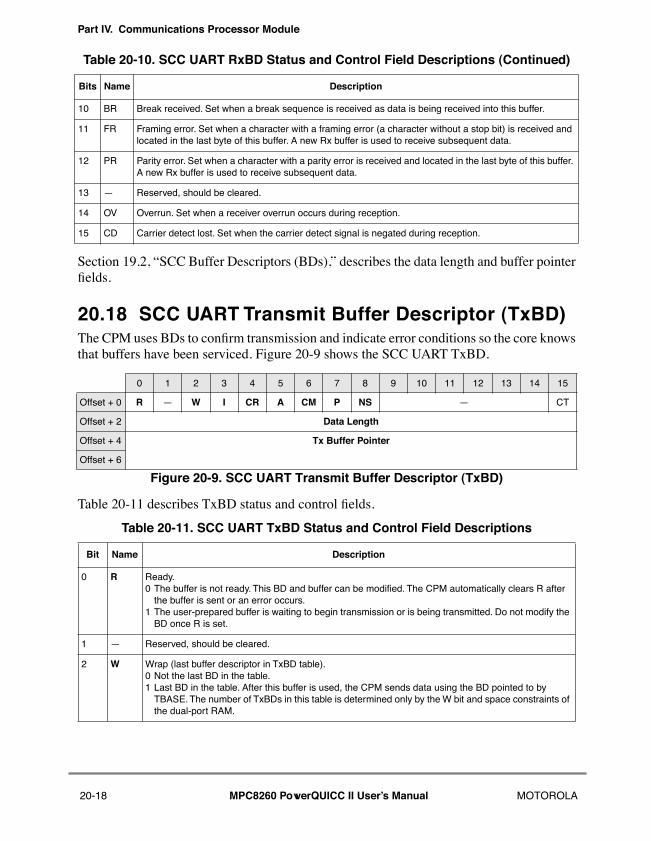
Part IV. Communications Processor Module
Section 19.2, ÒSCC Buffer Descriptors (BDs),Ó describes the data length and buffer pointerÞelds.
20.18 SCC UART Transmit Buffer Descriptor (TxBD)The CPM uses BDs to conÞrm transmission and indicate error conditions so the core knowsthat buffers have been serviced. Figure 20-9 shows the SCC UART TxBD.
Table 20-11 describes TxBD status and control Þelds.
10 BR Break received. Set when a break sequence is received as data is being received into this buffer.
11 FR Framing error. Set when a character with a framing error (a character without a stop bit) is received and located in the last byte of this buffer. A new Rx buffer is used to receive subsequent data.
12 PR Parity error. Set when a character with a parity error is received and located in the last byte of this buffer. A new Rx buffer is used to receive subsequent data.
13 Ñ Reserved, should be cleared.
14 OV Overrun. Set when a receiver overrun occurs during reception.
15 CD Carrier detect lost. Set when the carrier detect signal is negated during reception.
0 1 2 3 4 5 6 7 8 9 10 11 12 13 14 15
Offset + 0 R Ñ W I CR A CM P NS Ñ CT
Offset + 2 Data Length
Offset + 4 Tx Buffer Pointer
Offset + 6
Figure 20-9. SCC UART Transmit Buffer Descriptor (TxBD)
Table 20-11. SCC UART TxBD Status and Control Field Descriptions
Bit Name Description
0 R Ready. 0 The buffer is not ready. This BD and buffer can be modiÞed. The CPM automatically clears R after
the buffer is sent or an error occurs.1 The user-prepared buffer is waiting to begin transmission or is being transmitted. Do not modify the
BD once R is set.
1 Ñ Reserved, should be cleared.
2 W Wrap (last buffer descriptor in TxBD table). 0 Not the last BD in the table. 1 Last BD in the table. After this buffer is used, the CPM sends data using the BD pointed to by
TBASE. The number of TxBDs in this table is determined only by the W bit and space constraints of the dual-port RAM.
Table 20-10. SCC UART RxBD Status and Control Field Descriptions (Continued)
Bits Name Description
20-18 MPC8260 PowerQUICC II UserÕs Manual MOTOROLA
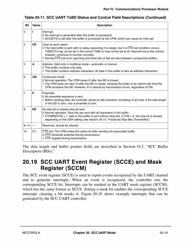
Part IV. Communications Processor Module
The data length and buffer pointer Þelds are described in Section 19.2, ÒSCC BufferDescriptors (BDs).Ó
20.19 SCC UART Event Register (SCCE) and Mask Register (SCCM)
The SCC event register (SCCE) is used to report events recognized by the UART channeland to generate interrupts. When an event is recognized, the controller sets thecorresponding SCCE bit. Interrupts can be masked in the UART mask register (SCCM),which has the same format as SCCE. Setting a mask bit enables the corresponding SCCEinterrupt; clearing a bit masks it. Figure 20-10 shows example interrupts that can begenerated by the SCC UART controller.
3 I Interrupt. 0 No interrupt is generated after this buffer is processed.1 SCCE[TX] is set after this buffer is processed by the CPM, which can cause an interrupt.
4 CR Clear-to-send report. 0 The next buffer is sent with no delay (assuming it is ready), but if a CTS lost condition occurs,
TxBD[CT] may not be set in the correct TxBD or may not be set at all. Asynchronous ßow control, however, continues to function normally.
1 Normal CTS lost error reporting and three bits of idle are sent between consecutive buffers.
5 A Address. Valid only in multidrop modeÑautomatic or manual.0 This buffer contains only data.1 This buffer contains address characters. All data in this buffer is sent as address characters.
6 CM Continuous mode. 0 Normal operation. The CPM clears R after this BD is closed.1 The CPM does not clear R after this BD is closed, allowing the buffer to be resent next time the
CPM accesses this BD. However, R is cleared by transmission errors, regardless of CM.
7 P Preamble. 0 No preamble sequence is sent.1 Before sending data, the controller sends an idle character consisting of all ones. If the data length
of this BD is zero, only a preamble is sent.
8 NS No stop bit or shaved stop bit sent. 0 Normal operation. Stop bits are sent with all characters in this buffer.1 If PSMR[SYN] = 1, data in this buffer is sent without stop bits. If SYN = 0, the stop bit is shaved,
depending on the DSR setting; see Section 20.14, ÒFractional Stop Bits (Transmitter).Ó
9Ð14 Ñ Reserved, should be cleared.
15 CT CTS lost. The CPM writes this status bit after sending the associated buffer. 0 CTS remained asserted during transmission.1 CTS negated during transmission.
Table 20-11. SCC UART TxBD Status and Control Field Descriptions (Continued)
Bit Name Description
MOTOROLA Chapter 20. SCC UART Mode 20-19
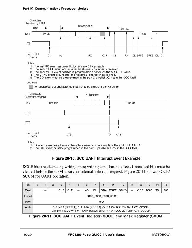
Part IV. Communications Processor Module
Figure 20-10. SCC UART Interrupt Event Example
SCCE bits are cleared by writing ones; writing zeros has no effect. Unmasked bits must becleared before the CPM clears an internal interrupt request. Figure 20-11 shows SCCE/SCCM for UART operation.
Bit 0 1 2 3 4 5 6 7 8 9 10 11 12 13 14 15
Field Ñ GLR GLT Ñ AB IDL GRA BRKE BRKS Ñ CCR BSY TX RX
Reset 0000_0000_0000_0000
R/W R/W
Addr 0x11A10 (SCCE1); 0x11A30 (SCCE2); 0x11A50 (SCCE3); 0x11A70 (SCCE4)0x11A14 (SCCM1); 0x11A34 (SCCM2); 0x11A54 (SCCM3); 0x11A74 (SCCM4)
Figure 20-11. SCC UART Event Register (SCCE) and Mask Register (SCCM)
CD IDL RX CCR IDL RX IDL BRKS BRKE IDL CD
Break
Line Idle10 Characters
RXD
CD
CharactersReceived by UART
Time
Line Idle
TXD
RTS
CharactersTransmitted by UART
CTS
TX CTSCTS
Line Idle Line Idle
7 Characters
Notes:
UART SCCEEvents
1. The first RX event assumes Rx buffers are 6 bytes each.2. The second IDL event occurs after an all-ones character is received.3. The second RX event position is programmable based on the MAX_IDL value.4. The BRKS event occurs after the first break character is received.5. The CD event must be programmed in the port C parallel I/O, not in the SCC itself.
Legend:
A receive control character defined not to be stored in the Rx buffer.
Notes:
UART SCCEEvents
1. TX event assumes all seven characters were put into a single buffer and TxBD[CR]=1.2. The CTS event must be programmed in the port C parallel I/O, not in the SCC itself.
20-20 MPC8260 PowerQUICC II UserÕs Manual MOTOROLA
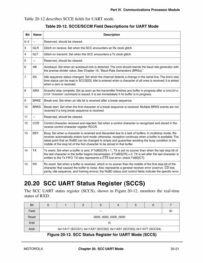
Part IV. Communications Processor Module
Table 20-12 describes SCCE Þelds for UART mode.
20.20 SCC UART Status Register (SCCS)The SCC UART status register (SCCS), shown in Figure 20-12, monitors the real-timestatus of RXD.
Table 20-12. SCCE/SCCM Field Descriptions for UART Mode
Bit Name Description
0Ð2 Ñ Reserved, should be cleared.
3 GLR Glitch on receive. Set when the SCC encounters an Rx clock glitch.
4 GLT Glitch on transmit. Set when the SCC encounters a Tx clock glitch.
5 Ñ Reserved, should be cleared.
6 AB Autobaud. Set when an autobaud lock is detected. The core should rewrite the baud rate generator with the precise divider value. See Chapter 16, ÒBaud-Rate Generators (BRGs).Ó
7 IDL Idle sequence status changed. Set when the channel detects a change in the serial line. The lineÕs real-time status can be read in SCCS[ID]. Idle is entered when a character of all ones is received; it is exited when a zero is received.
8 GRA Graceful stop complete. Set as soon as the transmitter Þnishes any buffer in progress after a GRACEFUL STOP TRANSMIT command is issued. It is set immediately if no buffer is in progress.
9 BRKE Break end. Set when an idle bit is received after a break sequence.
10 BRKS Break start. Set when the Þrst character of a break sequence is received. Multiple BRKS events are not received if a long break sequence is received.
11 Ñ Reserved, should be cleared.
12 CCR Control character received and rejected. Set when a control character is recognized and stored in the receive control character register RCCR.
13 BSY Busy. Set when a character is received and discarded due to a lack of buffers. In multidrop mode, the receiver automatically enters hunt mode; otherwise, reception continues when a buffer is available. The latest point that an RxBD can be changed to empty and guarantee avoiding the busy condition is the middle of the stop bit of the Þrst character to be stored in that buffer.
14 TX Tx event. Set when a buffer is sent. If TxBD[CR] = 1, TX is set no sooner than when the last stop bit of the last character in the buffer begins transmission. If TxBD[CR] = 0, TX is set after the last character is written to the Tx FIFO. TX also represents a CTS lost error; check TxBD[CT].
15 RX Rx event. Set when a buffer is received, which is no sooner than the middle of the Þrst stop bit of the character that caused the buffer to close. Also represents a general receiver error (overrun, CD lost, parity, idle sequence, and framing errors); the RxBD status and control Þelds indicate the speciÞc error.
Bit 0 1 2 3 4 5 6 7
Field Ñ ID
Reset 0000_0000_0000_0000
R/W R
Addr 0x11A17 (SCCS1); 0x11A37 (SCCS2); 0x11A57 (SCCS3); 0x11A77 (SCCS4)
Figure 20-12. SCC Status Register for UART Mode (SCCS)
MOTOROLA Chapter 20. SCC UART Mode 20-21
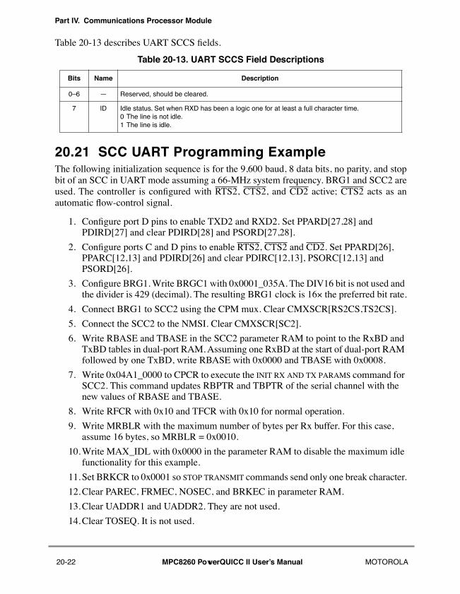
Part IV. Communications Processor Module
Table 20-13 describes UART SCCS Þelds.
20.21 SCC UART Programming ExampleThe following initialization sequence is for the 9,600 baud, 8 data bits, no parity, and stopbit of an SCC in UART mode assuming a 66-MHz system frequency. BRG1 and SCC2 areused. The controller is conÞgured with RTS2, CTS2, and CD2 active; CTS2 acts as anautomatic ßow-control signal.
1. ConÞgure port D pins to enable TXD2 and RXD2. Set PPARD[27,28] and PDIRD[27] and clear PDIRD[28] and PSORD[27,28].
2. ConÞgure ports C and D pins to enable RTS2, CTS2 and CD2. Set PPARD[26], PPARC[12,13] and PDIRD[26] and clear PDIRC[12,13], PSORC[12,13] and PSORD[26].
3. ConÞgure BRG1. Write BRGC1 with 0x0001_035A. The DIV16 bit is not used and the divider is 429 (decimal). The resulting BRG1 clock is 16´ the preferred bit rate.
4. Connect BRG1 to SCC2 using the CPM mux. Clear CMXSCR[RS2CS,TS2CS].
5. Connect the SCC2 to the NMSI. Clear CMXSCR[SC2].
6. Write RBASE and TBASE in the SCC2 parameter RAM to point to the RxBD and TxBD tables in dual-port RAM. Assuming one RxBD at the start of dual-port RAM followed by one TxBD, write RBASE with 0x0000 and TBASE with 0x0008.
7. Write 0x04A1_0000 to CPCR to execute the INIT RX AND TX PARAMS command for SCC2. This command updates RBPTR and TBPTR of the serial channel with the new values of RBASE and TBASE.
8. Write RFCR with 0x10 and TFCR with 0x10 for normal operation.
9. Write MRBLR with the maximum number of bytes per Rx buffer. For this case, assume 16 bytes, so MRBLR = 0x0010.
10. Write MAX_IDL with 0x0000 in the parameter RAM to disable the maximum idle functionality for this example.
11. Set BRKCR to 0x0001 so STOP TRANSMIT commands send only one break character.
12. Clear PAREC, FRMEC, NOSEC, and BRKEC in parameter RAM.
13. Clear UADDR1 and UADDR2. They are not used.
14. Clear TOSEQ. It is not used.
Table 20-13. UART SCCS Field Descriptions
Bits Name Description
0Ð6 Ñ Reserved, should be cleared.
7 ID Idle status. Set when RXD has been a logic one for at least a full character time.0 The line is not idle.1 The line is idle.
20-22 MPC8260 PowerQUICC II UserÕs Manual MOTOROLA
Part IV. Communications Processor Module
15. Write CHARACTER1Ð8 with 0x8000. They are not used.
16. Write RCCM with 0xC0FF. It is not used.
17. Initialize the RxBD. Assume the Rx buffer is at 0x0000_1000 in main memory. Write 0xB000 to the RxBD[Status and Control], 0x0000 to RxBD[Data Length] (optional), and 0x0000_1000 to RxBD[Buffer Pointer].
18. Initialize the TxBD. Assume the buffer is at 0x0000_2000 in main memory and contains sixteen 8-bit characters. Write 0xB000 to the TxBD[Status and Control], 0x0010 to TxBD[Data Length], and 0x00002000 to TxBD[Buffer Pointer].
19. Write 0xFFFF to SCCE2 to clear any previous events.
20. Write 0x0003 to SCCM2 to allow the TX and RX interrupts.
21. Write 0x0040_0000 to the SIMR_L so SMC1 can generate a system interrupt. Initialize SIPNR_L by writing 0xFFFF_FFFF to it.
22. Write 0x0000_0020 to GSMR_H2 to conÞgure a small Rx FIFO width.
23. Write 0x0002_8004 to GSMR_L2 to conÞgure 16´ sampling for transmit and receive, CTS and CD to automatically control transmission and reception (DIAG bits), and the SCC for UART mode. Notice that the transmitter (ENT) and receiver (ENR) have not been enabled yet.
24. Set PSMR2 to 0xB000 to conÞgure automatic ßow control using CTS, 8-bit characters, no parity, 1 stop bit, and asynchronous SCC UART operation.
25. Write 0x0002_8034 to GSMR_L2 to enable the transmitter and receiver. This ensures that ENT and ENR are enabled last.
Note that after 16 bytes are sent, the transmit buffer is closed. Additionally, the receivebuffer is closed after 16 bytes are received. Data received after 16 bytes causes a busy(out-of-buffers) condition because only one RxBD is prepared.
20.22 S-Records Loader ApplicationThis section describes a downloading application that uses an SCC UART controller. Theapplication performs S-record downloads and uploads between a host computer and anintelligent peripheral through a serial asynchronous line. S-records are strings of ASCIIcharacters that begin with ÔSÕ and end in an end-of-line character. This characteristic is usedto impose a message structure on the communication between the devices. For ßow control,each device can transmit XON and XOFF characters, which are not part of the programbeing uploaded or downloaded.
For simplicity, assume that the line is not multidrop (no addresses are sent) and that eachS-record Þts into a single buffer. Follow the basic UART initialization sequence above inSection 20.21, ÒSCC UART Programming Example,Ó except allow for more and largerbuffers and create the control character table as described in Table 20-14.
MOTOROLA Chapter 20. SCC UART Mode 20-23
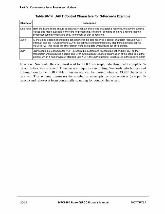
Part IV. Communications Processor Module
To receive S-records, the core must wait for an RX interrupt, indicating that a complete S-record buffer was received. Transmission requires assembling S-records into buffers andlinking them to the TxBD table; transmission can be paused when an XOFF character isreceived. This scheme minimizes the number of interrupts the core receives (one per S-record) and relieves it from continually scanning for control characters.
Table 20-14. UART Control Characters for S-Records Example
Character Description
Line Feed Both the E and R bits should be cleared. When an end-of-line character is received, the current buffer is closed and made available to the core for processing. This buffer contains an entire S record that the processor can now check and copy to memory or disk as required.
XOFF E should be cleared; R should be set. Whenever the core receives a control-character-received (CCR) interrupt and the RCCR contains XOFF, the software should immediately stop transmitting by setting PSMR[FRZ]. This keeps the other station from losing data when it runs out of Rx buffers.
XON XON should be received after XOFF. E should be cleared and R should be set. PSMR[FRZ] on the transmitter should now be cleared. The CPM automatically resumes transmission of the serial line at the point at which it was previously stopped. Like XOFF, the XON character is not stored in the receive buffer.
20-24 MPC8260 PowerQUICC II UserÕs Manual MOTOROLA
Chapter 21 SCC HDLC Mode210210
High-level data link control (HDLC) is one of the most common protocols in the data linklayer, layer 2 of the OSI model. Many other common layer 2 protocols, such as SDLC,SS#7, AppleTalk, LAPB, and LAPD, are based on HDLC and its framing structure inparticular. Figure 21-1 shows the HDLC framing structure.
HDLC uses a zero insertion/deletion process (bit-stufÞng) to ensure that a data bit patternmatching the delimiter ßag does not occur in a Þeld between ßags. The HDLC frame issynchronous and relies on the physical layer for clocking and synchronization of thetransmitter/receiver.
An address Þeld is needed to carry the frame's destination address because the layer 2 framecan be sent over point-to-point links, broadcast networks, packet-switched or circuit-switched systems. An address Þeld is commonly 0, 8, or 16 bits, depending on the data linklayer protocol. SDLC and LAPB use an 8-bit address. SS#7 has no address Þeld because itis always used in point-to-point signaling links. LAPD divides its 16-bit address intodifferent Þelds to specify various access points within one device. LAPD also deÞnes abroadcast address. Some HDLC-type protocols permit addressing beyond 16 bits.
The 8- or 16-bit control Þeld provides a ßow control number and deÞnes the frame type(control or data). The exact use and structure of this Þeld depends on the protocol using theframe. The length of the data in the data Þeld depends on the frame protocol. Layer 3 framesare carried in this data Þeld. Error control is implemented by appending a cyclic redundancycheck (CRC) to the frame, which in most protocols is 16 bits long but can be as long as 32bits. In HDLC, the lsb of each octet is sent Þrst; the msb of the CRC is sent Þrst.
HDLC mode is selected for an SCC by writing GSMR_L[MODE] = 0b0000. In anonmultiplexed modem interface, SCC outputs connect directly to external pins. Modemsignals can be supported through port C. The Rx and Tx clocks can be supplied from eitherthe bank of baud rate generators, by the DPLL, or externally. An SCC can also be connectedthrough the TDM channels of the serial interface (SI). In HDLC mode, an SCC becomesan HDLC controller, and consists of separate transmit and receive sections whoseoperations are asynchronous with the core and can either be synchronous or asynchronouswith respect to other SCCs.
MOTOROLA Chapter 21. SCC HDLC Mode 21-1
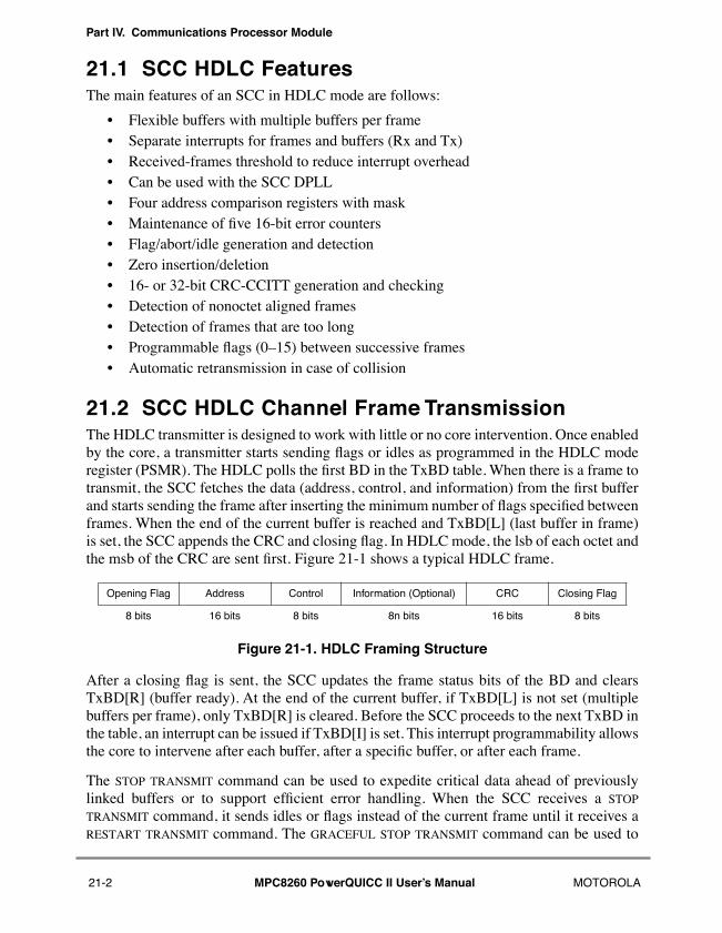
Part IV. Communications Processor Module
21.1 SCC HDLC FeaturesThe main features of an SCC in HDLC mode are follows:
¥ Flexible buffers with multiple buffers per frame¥ Separate interrupts for frames and buffers (Rx and Tx)¥ Received-frames threshold to reduce interrupt overhead¥ Can be used with the SCC DPLL¥ Four address comparison registers with mask¥ Maintenance of Þve 16-bit error counters¥ Flag/abort/idle generation and detection¥ Zero insertion/deletion¥ 16- or 32-bit CRC-CCITT generation and checking¥ Detection of nonoctet aligned frames¥ Detection of frames that are too long¥ Programmable ßags (0Ð15) between successive frames¥ Automatic retransmission in case of collision
21.2 SCC HDLC Channel Frame Transmission The HDLC transmitter is designed to work with little or no core intervention. Once enabledby the core, a transmitter starts sending ßags or idles as programmed in the HDLC moderegister (PSMR). The HDLC polls the Þrst BD in the TxBD table. When there is a frame totransmit, the SCC fetches the data (address, control, and information) from the Þrst bufferand starts sending the frame after inserting the minimum number of ßags speciÞed betweenframes. When the end of the current buffer is reached and TxBD[L] (last buffer in frame)is set, the SCC appends the CRC and closing ßag. In HDLC mode, the lsb of each octet andthe msb of the CRC are sent Þrst. Figure 21-1 shows a typical HDLC frame.
Figure 21-1. HDLC Framing Structure
After a closing ßag is sent, the SCC updates the frame status bits of the BD and clearsTxBD[R] (buffer ready). At the end of the current buffer, if TxBD[L] is not set (multiplebuffers per frame), only TxBD[R] is cleared. Before the SCC proceeds to the next TxBD inthe table, an interrupt can be issued if TxBD[I] is set. This interrupt programmability allowsthe core to intervene after each buffer, after a speciÞc buffer, or after each frame.
The STOP TRANSMIT command can be used to expedite critical data ahead of previouslylinked buffers or to support efÞcient error handling. When the SCC receives a STOP
TRANSMIT command, it sends idles or ßags instead of the current frame until it receives aRESTART TRANSMIT command. The GRACEFUL STOP TRANSMIT command can be used to
Opening Flag Address Control Information (Optional) CRC Closing Flag
8 bits 16 bits 8 bits 8n bits 16 bits 8 bits
21-2 MPC8260 PowerQUICC II UserÕs Manual MOTOROLA
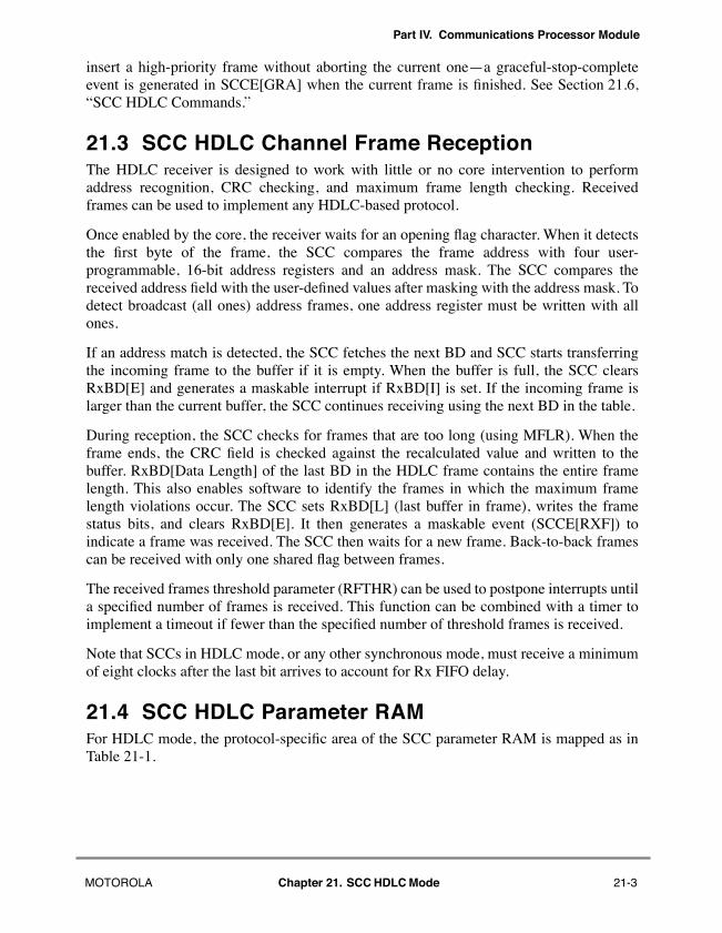
Part IV. Communications Processor Module
insert a high-priority frame without aborting the current oneÑa graceful-stop-completeevent is generated in SCCE[GRA] when the current frame is Þnished. See Section 21.6,ÒSCC HDLC Commands.Ó
21.3 SCC HDLC Channel Frame ReceptionThe HDLC receiver is designed to work with little or no core intervention to performaddress recognition, CRC checking, and maximum frame length checking. Receivedframes can be used to implement any HDLC-based protocol.
Once enabled by the core, the receiver waits for an opening ßag character. When it detectsthe Þrst byte of the frame, the SCC compares the frame address with four user-programmable, 16-bit address registers and an address mask. The SCC compares thereceived address Þeld with the user-deÞned values after masking with the address mask. Todetect broadcast (all ones) address frames, one address register must be written with allones.
If an address match is detected, the SCC fetches the next BD and SCC starts transferringthe incoming frame to the buffer if it is empty. When the buffer is full, the SCC clearsRxBD[E] and generates a maskable interrupt if RxBD[I] is set. If the incoming frame islarger than the current buffer, the SCC continues receiving using the next BD in the table.
During reception, the SCC checks for frames that are too long (using MFLR). When theframe ends, the CRC Þeld is checked against the recalculated value and written to thebuffer. RxBD[Data Length] of the last BD in the HDLC frame contains the entire framelength. This also enables software to identify the frames in which the maximum framelength violations occur. The SCC sets RxBD[L] (last buffer in frame), writes the framestatus bits, and clears RxBD[E]. It then generates a maskable event (SCCE[RXF]) toindicate a frame was received. The SCC then waits for a new frame. Back-to-back framescan be received with only one shared ßag between frames.
The received frames threshold parameter (RFTHR) can be used to postpone interrupts untila speciÞed number of frames is received. This function can be combined with a timer toimplement a timeout if fewer than the speciÞed number of threshold frames is received.
Note that SCCs in HDLC mode, or any other synchronous mode, must receive a minimumof eight clocks after the last bit arrives to account for Rx FIFO delay.
21.4 SCC HDLC Parameter RAMFor HDLC mode, the protocol-speciÞc area of the SCC parameter RAM is mapped as inTable 21-1.
MOTOROLA Chapter 21. SCC HDLC Mode 21-3
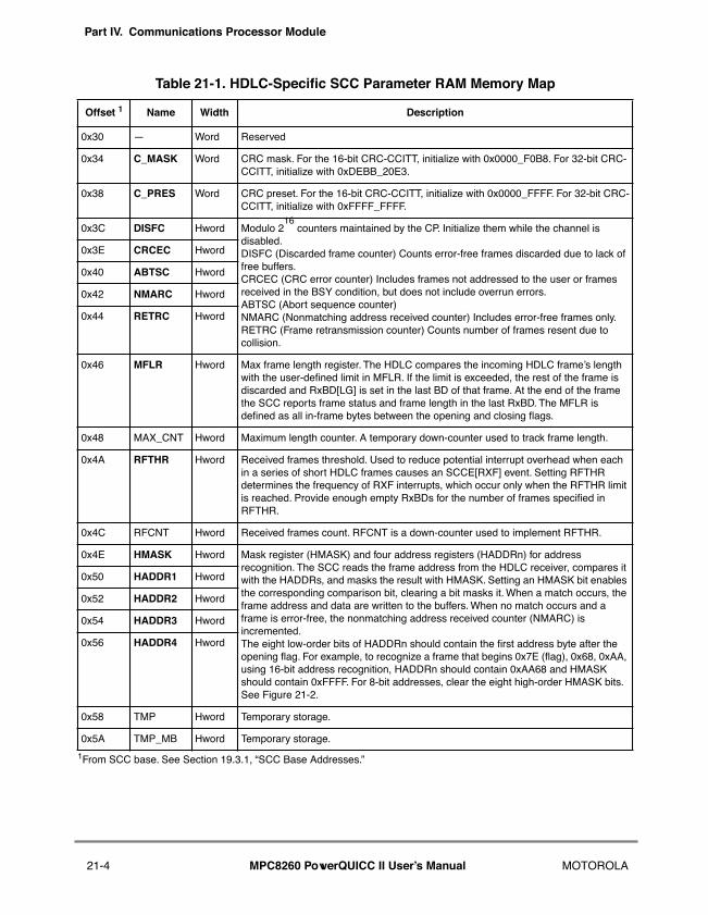
Part IV. Communications Processor Module
Table 21-1. HDLC-Specific SCC Parameter RAM Memory Map
Offset 1
1From SCC base. See Section 19.3.1, ÒSCC Base Addresses.Ó
Name Width Description
0x30 Ñ Word Reserved
0x34 C_MASK Word CRC mask. For the 16-bit CRC-CCITT, initialize with 0x0000_F0B8. For 32-bit CRC-CCITT, initialize with 0xDEBB_20E3.
0x38 C_PRES Word CRC preset. For the 16-bit CRC-CCITT, initialize with 0x0000_FFFF. For 32-bit CRC-CCITT, initialize with 0xFFFF_FFFF.
0x3C DISFC Hword Modulo 216
counters maintained by the CP. Initialize them while the channel is disabled.DISFC (Discarded frame counter) Counts error-free frames discarded due to lack of free buffers.CRCEC (CRC error counter) Includes frames not addressed to the user or frames received in the BSY condition, but does not include overrun errors.ABTSC (Abort sequence counter)NMARC (Nonmatching address received counter) Includes error-free frames only.RETRC (Frame retransmission counter) Counts number of frames resent due to collision.
0x3E CRCEC Hword
0x40 ABTSC Hword
0x42 NMARC Hword
0x44 RETRC Hword
0x46 MFLR Hword Max frame length register. The HDLC compares the incoming HDLC frameÕs length with the user-deÞned limit in MFLR. If the limit is exceeded, the rest of the frame is discarded and RxBD[LG] is set in the last BD of that frame. At the end of the frame the SCC reports frame status and frame length in the last RxBD. The MFLR is deÞned as all in-frame bytes between the opening and closing ßags.
0x48 MAX_CNT Hword Maximum length counter. A temporary down-counter used to track frame length.
0x4A RFTHR Hword Received frames threshold. Used to reduce potential interrupt overhead when each in a series of short HDLC frames causes an SCCE[RXF] event. Setting RFTHR determines the frequency of RXF interrupts, which occur only when the RFTHR limit is reached. Provide enough empty RxBDs for the number of frames speciÞed in RFTHR.
0x4C RFCNT Hword Received frames count. RFCNT is a down-counter used to implement RFTHR.
0x4E HMASK Hword Mask register (HMASK) and four address registers (HADDRn) for address recognition. The SCC reads the frame address from the HDLC receiver, compares it with the HADDRs, and masks the result with HMASK. Setting an HMASK bit enables the corresponding comparison bit, clearing a bit masks it. When a match occurs, the frame address and data are written to the buffers. When no match occurs and a frame is error-free, the nonmatching address received counter (NMARC) is incremented.The eight low-order bits of HADDRn should contain the Þrst address byte after the opening ßag. For example, to recognize a frame that begins 0x7E (ßag), 0x68, 0xAA, using 16-bit address recognition, HADDRn should contain 0xAA68 and HMASK should contain 0xFFFF. For 8-bit addresses, clear the eight high-order HMASK bits. See Figure 21-2.
0x50 HADDR1 Hword
0x52 HADDR2 Hword
0x54 HADDR3 Hword
0x56 HADDR4 Hword
0x58 TMP Hword Temporary storage.
0x5A TMP_MB Hword Temporary storage.
21-4 MPC8260 PowerQUICC II UserÕs Manual MOTOROLA
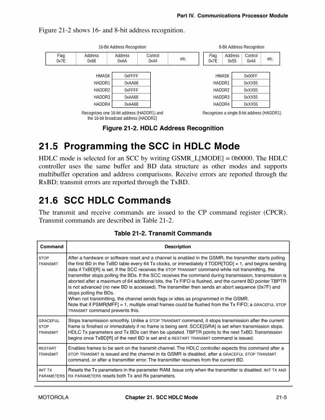
Part IV. Communications Processor Module
Figure 21-2 shows 16- and 8-bit address recognition.
Figure 21-2. HDLC Address Recognition
21.5 Programming the SCC in HDLC ModeHDLC mode is selected for an SCC by writing GSMR_L[MODE] = 0b0000. The HDLCcontroller uses the same buffer and BD data structure as other modes and supportsmultibuffer operation and address comparisons. Receive errors are reported through theRxBD; transmit errors are reported through the TxBD.
21.6 SCC HDLC CommandsThe transmit and receive commands are issued to the CP command register (CPCR).Transmit commands are described in Table 21-2.
Table 21-2. Transmit Commands
Command Description
STOP TRANSMIT
After a hardware or software reset and a channel is enabled in the GSMR, the transmitter starts polling the Þrst BD in the TxBD table every 64 Tx clocks, or immediately if TODR[TOD] = 1, and begins sending data if TxBD[R] is set. If the SCC receives the STOP TRANSMIT command while not transmitting, the transmitter stops polling the BDs. If the SCC receives the command during transmission, transmission is aborted after a maximum of 64 additional bits, the Tx FIFO is ßushed, and the current BD pointer TBPTR is not advanced (no new BD is accessed). The transmitter then sends an abort sequence (0x7F) and stops polling the BDs.When not transmitting, the channel sends ßags or idles as programmed in the GSMR.Note that if PSMR[MFF] = 1, multiple small frames could be ßushed from the Tx FIFO; a GRACEFUL STOP TRANSMIT command prevents this.
GRACEFUL STOP TRANSMIT
Stops transmission smoothly. Unlike a STOP TRANSMIT command, it stops transmission after the current frame is Þnished or immediately if no frame is being sent. SCCE[GRA] is set when transmission stops. HDLC Tx parameters and Tx BDs can then be updated. TBPTR points to the next TxBD. Transmission begins once TxBD[R] of the next BD is set and a RESTART TRANSMIT command is issued.
RESTART TRANSMIT
Enables frames to be sent on the transmit channel. The HDLC controller expects this command after a STOP TRANSMIT is issued and the channel in its GSMR is disabled, after a GRACEFUL STOP TRANSMIT command, or after a transmitter error. The transmitter resumes from the current BD.
INIT TX PARAMETERS
Resets the Tx parameters in the parameter RAM. Issue only when the transmitter is disabled. INIT TX AND RX PARAMETERS resets both Tx and Rx parameters.
Flag0x7E etc.
Flag0x7E
Address0x68
Address0xAA
Control0x44 etc.
Address0x55
Control0x44
16-Bit Address Recognition 8-Bit Address Recognition
0x00FFHMASK
0xXX55HADDR1
0xXX55HADDR2
0xXX55HADDR3
0xXX55HADDR4
0xFFFFHMASK
0xAA68HADDR1
0xFFFFHADDR2
0xAA68HADDR3
0xAA68HADDR4
Recognizes one 16-bit address (HADDR1) andthe 16-bit broadcast address (HADDR2)
Recognizes a single 8-bit address (HADDR1)
MOTOROLA Chapter 21. SCC HDLC Mode 21-5
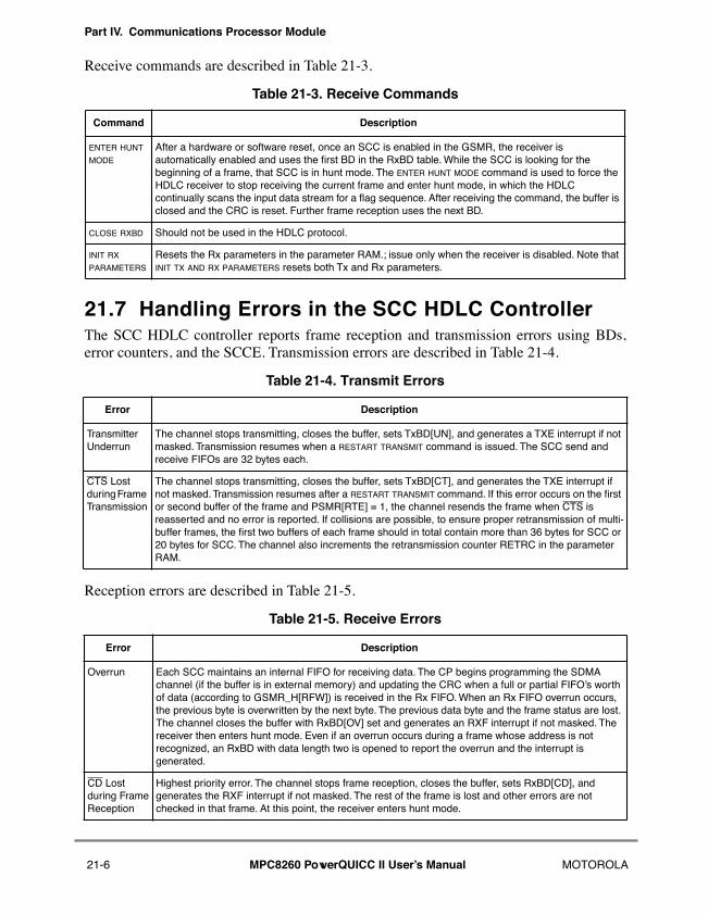
Part IV. Communications Processor Module
Receive commands are described in Table 21-3.
21.7 Handling Errors in the SCC HDLC ControllerThe SCC HDLC controller reports frame reception and transmission errors using BDs,error counters, and the SCCE. Transmission errors are described in Table 21-4.
Reception errors are described in Table 21-5.
Table 21-3. Receive Commands
Command Description
ENTER HUNT MODE
After a hardware or software reset, once an SCC is enabled in the GSMR, the receiver is automatically enabled and uses the Þrst BD in the RxBD table. While the SCC is looking for the beginning of a frame, that SCC is in hunt mode. The ENTER HUNT MODE command is used to force the HDLC receiver to stop receiving the current frame and enter hunt mode, in which the HDLC continually scans the input data stream for a ßag sequence. After receiving the command, the buffer is closed and the CRC is reset. Further frame reception uses the next BD.
CLOSE RXBD Should not be used in the HDLC protocol.
INIT RX PARAMETERS
Resets the Rx parameters in the parameter RAM.; issue only when the receiver is disabled. Note that INIT TX AND RX PARAMETERS resets both Tx and Rx parameters.
Table 21-4. Transmit Errors
Error Description
Transmitter Underrun
The channel stops transmitting, closes the buffer, sets TxBD[UN], and generates a TXE interrupt if not masked. Transmission resumes when a RESTART TRANSMIT command is issued. The SCC send and receive FIFOs are 32 bytes each.
CTS Lost during Frame Transmission
The channel stops transmitting, closes the buffer, sets TxBD[CT], and generates the TXE interrupt if not masked. Transmission resumes after a RESTART TRANSMIT command. If this error occurs on the Þrst or second buffer of the frame and PSMR[RTE] = 1, the channel resends the frame when CTS is reasserted and no error is reported. If collisions are possible, to ensure proper retransmission of multi-buffer frames, the Þrst two buffers of each frame should in total contain more than 36 bytes for SCC or 20 bytes for SCC. The channel also increments the retransmission counter RETRC in the parameter RAM.
Table 21-5. Receive Errors
Error Description
Overrun Each SCC maintains an internal FIFO for receiving data. The CP begins programming the SDMA channel (if the buffer is in external memory) and updating the CRC when a full or partial FIFOÕs worth of data (according to GSMR_H[RFW]) is received in the Rx FIFO. When an Rx FIFO overrun occurs, the previous byte is overwritten by the next byte. The previous data byte and the frame status are lost. The channel closes the buffer with RxBD[OV] set and generates an RXF interrupt if not masked. The receiver then enters hunt mode. Even if an overrun occurs during a frame whose address is not recognized, an RxBD with data length two is opened to report the overrun and the interrupt is generated.
CD Lost during FrameReception
Highest priority error. The channel stops frame reception, closes the buffer, sets RxBD[CD], and generates the RXF interrupt if not masked. The rest of the frame is lost and other errors are not checked in that frame. At this point, the receiver enters hunt mode.
21-6 MPC8260 PowerQUICC II UserÕs Manual MOTOROLA
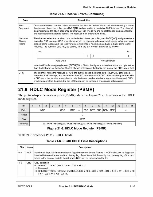
Part IV. Communications Processor Module
21.8 HDLC Mode Register (PSMR)The protocol-speciÞc mode register (PSMR), shown in Figure 21-3, functions as the HDLCmode register.
Table 21-6 describes PSMR HDLC Þelds.
Abort Sequence
Occurs when seven or more consecutive ones are received. When this occurs while receiving a frame, the channel closes the buffer, sets RxBD[AB] and generates a maskable RXF interrupt. The channel also increments the abort sequence counter ABTSC. The CRC and nonoctet error status conditions are not checked on aborted frames. The receiver then enters hunt mode.
Nonoctet Aligned Frame
The channel writes the received data to the buffer, closes the buffer, sets RxBD[NO], and generates a maskable RXF interrupt. CRC error status should be disregarded on nonoctet frames. After a nonoctet aligned frame is received, the receiver enters hunt mode. An immediate back-to-back frame is still received. The nonoctet data may be derived from the last word in the buffer as follows:
Note that if buffer swapping is used (RFCR[BO] = 0b0x), the Þgure above refers to the last byte, rather than the last word, of the buffer. The lsb of each octet is sent Þrst while the msb of the CRC is sent Þrst.
CRC The channel writes the received CRC to the buffer, closes the buffer, sets RxBD[CR], generates a maskable RXF interrupt, and increments the CRC error counter CRCEC. After receiving a frame with a CRC error, the receiver enters hunt mode. An immediate back-to-back frame is still received. CRC checking cannot be disabled, but the CRC error can be ignored if checking is not required.
Bit 0 1 2 3 4 5 6 7 8 9 10 11 12 13 14 15
Field NOF CRC RTE Ñ FSE DRT BUS BRM MFF Ñ
Reset 0
R/W R/W
Address 0x11A08 (PSMR1); 0x11A28 (PSMR2); 0x11A48 (PSMR3); 0x11A68 (PSMR4)
Figure 21-3. HDLC Mode Register (PSMR)
Table 21-6. PSMR HDLC Field Descriptions
Bits Name Description
0-3 NOF Number of ßags. Minimum number of ßags between or before frames. If NOF = 0b0000, no ßags are inserted between frames and the closing ßag of one frame is followed by the opening ßag of the next frame in the case of back-to-back frames. NOF can be modiÞed on-the-ßy.
4Ð5 CRC CRC selection. 00 16-bit CCITT-CRC (HDLC). X16 + X12 + X5 + 1.x1 Reserved.10 32-bit CCITT-CRC (Ethernet and HDLC). X32 + X26 + X23 + X22 + X16 + X12 + X11 + X10 + X8
+ X7 + X5 + X4 + X2 + X1 +1.
Table 21-5. Receive Errors (Continued)
Error Description
msb lsb
1 0 0
Valid Data Nonvalid Data
MOTOROLA Chapter 21. SCC HDLC Mode 21-7
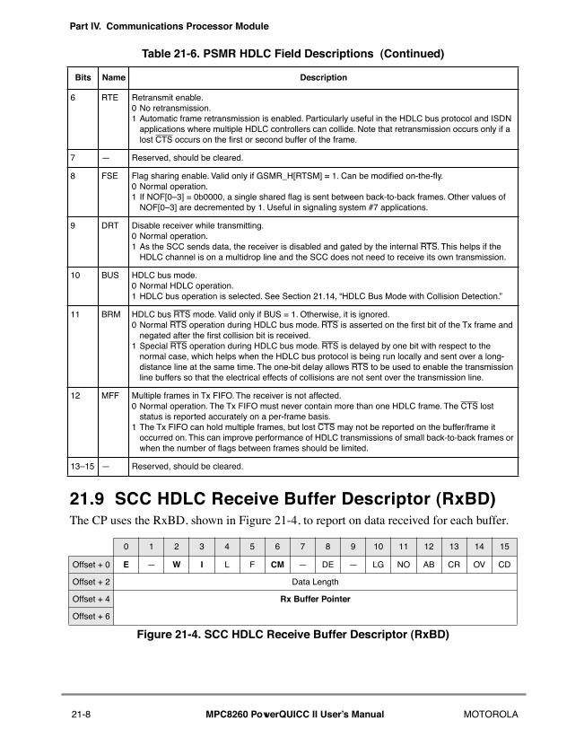
Part IV. Communications Processor Module
21.9 SCC HDLC Receive Buffer Descriptor (RxBD)The CP uses the RxBD, shown in Figure 21-4, to report on data received for each buffer.
6 RTE Retransmit enable. 0 No retransmission.1 Automatic frame retransmission is enabled. Particularly useful in the HDLC bus protocol and ISDN
applications where multiple HDLC controllers can collide. Note that retransmission occurs only if a lost CTS occurs on the Þrst or second buffer of the frame.
7 Ñ Reserved, should be cleared.
8 FSE Flag sharing enable. Valid only if GSMR_H[RTSM] = 1. Can be modiÞed on-the-ßy.0 Normal operation.1 If NOF[0Ð3] = 0b0000, a single shared ßag is sent between back-to-back frames. Other values of
NOF[0Ð3] are decremented by 1. Useful in signaling system #7 applications.
9 DRT Disable receiver while transmitting. 0 Normal operation.1 As the SCC sends data, the receiver is disabled and gated by the internal RTS. This helps if the
HDLC channel is on a multidrop line and the SCC does not need to receive its own transmission.
10 BUS HDLC bus mode. 0 Normal HDLC operation.1 HDLC bus operation is selected. See Section 21.14, ÒHDLC Bus Mode with Collision Detection.Ó
11 BRM HDLC bus RTS mode. Valid only if BUS = 1. Otherwise, it is ignored.0 Normal RTS operation during HDLC bus mode. RTS is asserted on the Þrst bit of the Tx frame and
negated after the Þrst collision bit is received. 1 Special RTS operation during HDLC bus mode. RTS is delayed by one bit with respect to the
normal case, which helps when the HDLC bus protocol is being run locally and sent over a long-distance line at the same time. The one-bit delay allows RTS to be used to enable the transmission line buffers so that the electrical effects of collisions are not sent over the transmission line.
12 MFF Multiple frames in Tx FIFO. The receiver is not affected.0 Normal operation. The Tx FIFO must never contain more than one HDLC frame. The CTS lost
status is reported accurately on a per-frame basis.1 The Tx FIFO can hold multiple frames, but lost CTS may not be reported on the buffer/frame it
occurred on. This can improve performance of HDLC transmissions of small back-to-back frames or when the number of ßags between frames should be limited.
13Ð15 Ñ Reserved, should be cleared.
0 1 2 3 4 5 6 7 8 9 10 11 12 13 14 15
Offset + 0 E Ñ W I L F CM Ñ DE Ñ LG NO AB CR OV CD
Offset + 2 Data Length
Offset + 4 Rx Buffer Pointer
Offset + 6
Figure 21-4. SCC HDLC Receive Buffer Descriptor (RxBD)
Table 21-6. PSMR HDLC Field Descriptions (Continued)
Bits Name Description
21-8 MPC8260 PowerQUICC II UserÕs Manual MOTOROLA
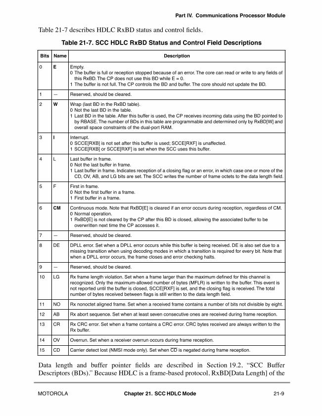
Part IV. Communications Processor Module
Table 21-7 describes HDLC RxBD status and control Þelds.
Data length and buffer pointer Þelds are described in Section 19.2, ÒSCC BufferDescriptors (BDs).Ó Because HDLC is a frame-based protocol, RxBD[Data Length] of the
Table 21-7. SCC HDLC RxBD Status and Control Field Descriptions
Bits Name Description
0 E Empty. 0 The buffer is full or reception stopped because of an error. The core can read or write to any Þelds of
this RxBD. The CP does not use this BD while E = 0.1 The buffer is not full. The CP controls the BD and buffer. The core should not update the BD.
1 Ñ Reserved, should be cleared.
2 W Wrap (last BD in the RxBD table). 0 Not the last BD in the table. 1 Last BD in the table. After this buffer is used, the CP receives incoming data using the BD pointed to
by RBASE. The number of BDs in this table are programmable and determined only by RxBD[W] and overall space constraints of the dual-port RAM.
3 I Interrupt. 0 SCCE[RXB] is not set after this buffer is used; SCCE[RXF] is unaffected.1 SCCE[RXB] or SCCE[RXF] is set when the SCC uses this buffer.
4 L Last buffer in frame. 0 Not the last buffer in frame. 1 Last buffer in frame. Indicates reception of a closing ßag or an error, in which case one or more of the
CD, OV, AB, and LG bits are set. The SCC writes the number of frame octets to the data length Þeld.
5 F First in frame. 0 Not the Þrst buffer in a frame. 1 First buffer in a frame.
6 CM Continuous mode. Note that RxBD[E] is cleared if an error occurs during reception, regardless of CM.0 Normal operation.1 RxBD[E] is not cleared by the CP after this BD is closed, allowing the associated buffer to be
overwritten next time the CP accesses it.
7 Ñ Reserved, should be cleared.
8 DE DPLL error. Set when a DPLL error occurs while this buffer is being received. DE is also set due to a missing transition when using decoding modes in which a transition is required for every bit. Note that when a DPLL error occurs, the frame closes and error checking halts.
9 Ñ Reserved, should be cleared.
10 LG Rx frame length violation. Set when a frame larger than the maximum deÞned for this channel is recognized. Only the maximum-allowed number of bytes (MFLR) is written to the buffer. This event is not reported until the buffer is closed, SCCE[RXF] is set, and the closing ßag is received. The total number of bytes received between ßags is still written to the data length Þeld.
11 NO Rx nonoctet aligned frame. Set when a received frame contains a number of bits not divisible by eight.
12 AB Rx abort sequence. Set when at least seven consecutive ones are received during frame reception.
13 CR Rx CRC error. Set when a frame contains a CRC error. CRC bytes received are always written to the Rx buffer.
14 OV Overrun. Set when a receiver overrun occurs during frame reception.
15 CD Carrier detect lost (NMSI mode only). Set when CD is negated during frame reception.
MOTOROLA Chapter 21. SCC HDLC Mode 21-9
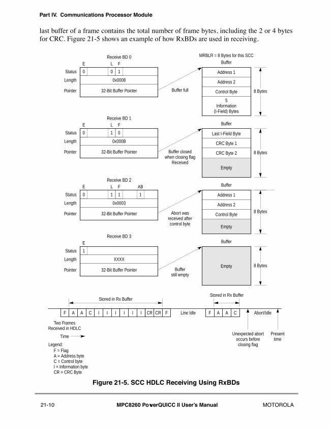
Part IV. Communications Processor Module
last buffer of a frame contains the total number of frame bytes, including the 2 or 4 bytesfor CRC. Figure 21-5 shows an example of how RxBDs are used in receiving.
Figure 21-5. SCC HDLC Receiving Using RxBDs
Buffer
0
0x0008
32-Bit Buffer Pointer
1
E FReceive BD 0
Status
Length
Pointer
0
0x000B
32-Bit Buffer Pointer
0
E FReceive BD 1
Status
Length
Pointer
0
0x0003
32-Bit Buffer Pointer
1
E FReceive BD 2
Status
Length
Pointer
1
XXXX
32-Bit Buffer Pointer
EReceive BD 3
Status
Length
Pointer
Address 1
Address 2
Control Byte
Buffer
CRC Byte 1
CRC Byte 2
Buffer
Address 1
Address 2
Buffer
Control Byte
Empty
8 Bytes
8 Bytes
8 Bytes
8 Bytes
Two FramesReceived in HDLC
Unexpected abort
Stored in Rx Buffer
Line Idle
occurs beforePresent
timeTime
Stored in Rx Buffer
Buffer full
Buffer closedwhen closing flag
Bufferstill empty
1
AB
5
Empty
MRBLR = 8 Bytes for this SCC
Empty
Last I-Field Byte
Information(I-Field) Bytes
Received
Abort wasreceived aftercontrol byte
0
L
1
L
1
L
F A A C I I I I I I CR CR F
closing flag
Abort/IdleF A A C
Legend:F = FlagA = Address byteC = Control byteI = Information byteCR = CRC Byte
21-10 MPC8260 PowerQUICC II UserÕs Manual MOTOROLA
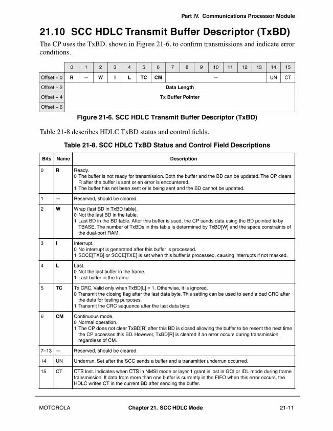
Part IV. Communications Processor Module
21.10 SCC HDLC Transmit Buffer Descriptor (TxBD)The CP uses the TxBD, shown in Figure 21-6, to conÞrm transmissions and indicate errorconditions.
Table 21-8 describes HDLC TxBD status and control Þelds.
0 1 2 3 4 5 6 7 8 9 10 11 12 13 14 15
Offset + 0 R Ñ W I L TC CM Ñ UN CT
Offset + 2 Data Length
Offset + 4 Tx Buffer Pointer
Offset + 6
Figure 21-6. SCC HDLC Transmit Buffer Descriptor (TxBD)
Table 21-8. SCC HDLC TxBD Status and Control Field Descriptions
Bits Name Description
0 R Ready. 0 The buffer is not ready for transmission. Both the buffer and the BD can be updated. The CP clears
R after the buffer is sent or an error is encountered.1 The buffer has not been sent or is being sent and the BD cannot be updated.
1 Ñ Reserved, should be cleared.
2 W Wrap (last BD in TxBD table). 0 Not the last BD in the table. 1 Last BD in the BD table. After this buffer is used, the CP sends data using the BD pointed to by
TBASE. The number of TxBDs in this table is determined by TxBD[W] and the space constraints of the dual-port RAM.
3 I Interrupt. 0 No interrupt is generated after this buffer is processed.1 SCCE[TXB] or SCCE[TXE] is set when this buffer is processed, causing interrupts if not masked.
4 L Last. 0 Not the last buffer in the frame. 1 Last buffer in the frame.
5 TC Tx CRC. Valid only when TxBD[L] = 1. Otherwise, it is ignored.0 Transmit the closing ßag after the last data byte. This setting can be used to send a bad CRC after
the data for testing purposes. 1 Transmit the CRC sequence after the last data byte.
6 CM Continuous mode. 0 Normal operation.1 The CP does not clear TxBD[R] after this BD is closed allowing the buffer to be resent the next time
the CP accesses this BD. However, TxBD[R] is cleared if an error occurs during transmission, regardless of CM.
7Ð13 Ñ Reserved, should be cleared.
14 UN Underrun. Set after the SCC sends a buffer and a transmitter underrun occurred.
15 CT CTS lost. Indicates when CTS in NMSI mode or layer 1 grant is lost in GCI or IDL mode during frame transmission. If data from more than one buffer is currently in the FIFO when this error occurs, the HDLC writes CT in the current BD after sending the buffer.
MOTOROLA Chapter 21. SCC HDLC Mode 21-11
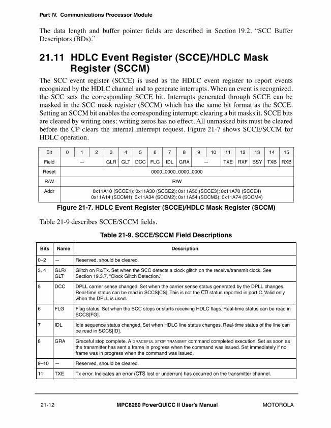
Part IV. Communications Processor Module
The data length and buffer pointer Þelds are described in Section 19.2, ÒSCC BufferDescriptors (BDs).Ó
21.11 HDLC Event Register (SCCE)/HDLC Mask Register (SCCM)
The SCC event register (SCCE) is used as the HDLC event register to report eventsrecognized by the HDLC channel and to generate interrupts. When an event is recognized,the SCC sets the corresponding SCCE bit. Interrupts generated through SCCE can bemasked in the SCC mask register (SCCM) which has the same bit format as the SCCE.Setting an SCCM bit enables the corresponding interrupt; clearing a bit masks it. SCCE bitsare cleared by writing ones; writing zeros has no effect. All unmasked bits must be clearedbefore the CP clears the internal interrupt request. Figure 21-7 shows SCCE/SCCM forHDLC operation.
Table 21-9 describes SCCE/SCCM Þelds.
Bit 0 1 2 3 4 5 6 7 8 9 10 11 12 13 14 15
Field Ñ GLR GLT DCC FLG IDL GRA Ñ TXE RXF BSY TXB RXB
Reset 0000_0000_0000_0000
R/W R/W
Addr 0x11A10 (SCCE1); 0x11A30 (SCCE2); 0x11A50 (SCCE3); 0x11A70 (SCCE4)0x11A14 (SCCM1); 0x11A34 (SCCM2); 0x11A54 (SCCM3); 0x11A74 (SCCM4)
Figure 21-7. HDLC Event Register (SCCE)/HDLC Mask Register (SCCM)
Table 21-9. SCCE/SCCM Field Descriptions
Bits Name Description
0Ð2 Ñ Reserved, should be cleared.
3, 4 GLR/GLT
Glitch on Rx/Tx. Set when the SCC detects a clock glitch on the receive/transmit clock. See Section 19.3.7, ÒClock Glitch Detection.Ó
5 DCC DPLL carrier sense changed. Set when the carrier sense status generated by the DPLL changes. Real-time status can be read in SCCS[CS]. This is not the CD status reported in port C. Valid only when the DPLL is used.
6 FLG Flag status. Set when the SCC stops or starts receiving HDLC ßags. Real-time status can be read in SCCS[FG].
7 IDL Idle sequence status changed. Set when HDLC line status changes. Real-time status of the line can be read in SCCS[ID].
8 GRA Graceful stop complete. A GRACEFUL STOP TRANSMIT command completed execution. Set as soon as the transmitter has sent a frame in progress when the command was issued. Set immediately if no frame was in progress when the command was issued.
9Ð10 Ñ Reserved, should be cleared.
11 TXE Tx error. Indicates an error (CTS lost or underrun) has occurred on the transmitter channel.
21-12 MPC8260 PowerQUICC II UserÕs Manual MOTOROLA
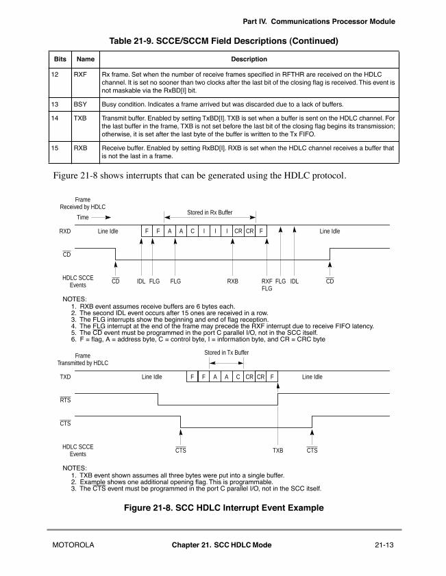
Part IV. Communications Processor Module
Figure 21-8 shows interrupts that can be generated using the HDLC protocol.
Figure 21-8. SCC HDLC Interrupt Event Example
12 RXF Rx frame. Set when the number of receive frames speciÞed in RFTHR are received on the HDLC channel. It is set no sooner than two clocks after the last bit of the closing ßag is received. This event is not maskable via the RxBD[I] bit.
13 BSY Busy condition. Indicates a frame arrived but was discarded due to a lack of buffers.
14 TXB Transmit buffer. Enabled by setting TxBD[I]. TXB is set when a buffer is sent on the HDLC channel. For the last buffer in the frame, TXB is not set before the last bit of the closing ßag begins its transmission; otherwise, it is set after the last byte of the buffer is written to the Tx FIFO.
15 RXB Receive buffer. Enabled by setting RxBD[I]. RXB is set when the HDLC channel receives a buffer that is not the last in a frame.
Table 21-9. SCCE/SCCM Field Descriptions (Continued)
Bits Name Description
CD IDL FLG RXB RXF IDL CD
Line Idle
Stored in Rx Buffer
RXD
CD
FrameReceived by HDLC
Time
Line Idle
TXD
RTS
FrameTransmitted by HDLC
CTS
TXB CTSCTS
Line Idle Line Idle
Stored in Tx Buffer
NOTES:
HDLC SCCEEvents
1. RXB event assumes receive buffers are 6 bytes each.2. The second IDL event occurs after 15 ones are received in a row.3. The FLG interrupts show the beginning and end of flag reception.4. The FLG interrupt at the end of the frame may precede the RXF interrupt due to receive FIFO latency.5. The CD event must be programmed in the port C parallel I/O, not in the SCC itself.
NOTES:
HDLC SCCEEvents
1. TXB event shown assumes all three bytes were put into a single buffer.2. Example shows one additional opening flag. This is programmable.
FF A A C I I I CR CR F
FLG FLGFLG
6. F = flag, A = address byte, C = control byte, I = information byte, and CR = CRC byte
F F A A C CR CR F
3. The CTS event must be programmed in the port C parallel I/O, not in the SCC itself.
MOTOROLA Chapter 21. SCC HDLC Mode 21-13
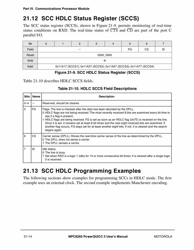
Part IV. Communications Processor Module
21.12 SCC HDLC Status Register (SCCS)The SCC status register (SCCS), shown in Figure 21-9, permits monitoring of real-timestatus conditions on RXD. The real-time status of CTS and CD are part of the port Cparallel I/O.
Table 21-10 describes HDLC SCCS Þelds.
21.13 SCC HDLC Programming ExamplesThe following sections show examples for programming SCCs in HDLC mode. The Þrstexample uses an external clock. The second example implements Manchester encoding.
Bit 0 1 2 3 4 5 6 7
Field Ñ FG CS ID
Reset 0000_0000
R/W R
Addr 0x11A17 (SCCS1); 0x11A37 (SCCS2); 0x11A57 (SCCS3); 0x11A77 (SCCS4)
Figure 21-9. SCC HDLC Status Register (SCCS)
Table 21-10. HDLC SCCS Field Descriptions
Bits Name Description
0Ð4 Ñ Reserved, should be cleared.
5 FG Flags. The line is checked after the data has been decoded by the DPLL.0 HDLC ßags are not being received. The most recently received 8 bits are examined every bit time to
see if a ßag is present. 1 HDLC ßags are being received. FG is set as soon as an HDLC ßag (0x7E) is received on the line.
Once it is set, it remains set at least 8 bit times and the next eight received bits are examined. If another ßag occurs, FG stays set for at least another eight bits. If not, it is cleared and the search begins again.
6 CS Carrier sense (DPLL). Shows the real-time carrier sense of the line as determined by the DPLL. 0 The DPLL does not sense a carrier.1 The DPLL senses a carrier.
7 ID Idle status. 0 The line is busy.1 Set when RXD is a logic 1 (idle) for 15 or more consecutive bit times. It is cleared after a single logic
0 is received.
21-14 MPC8260 PowerQUICC II UserÕs Manual MOTOROLA
Part IV. Communications Processor Module
21.13.1 SCC HDLC Programming Example #1The following initialization sequence is for an SCC HDLC channel with an external clock.SCC2 is used with RTS2, CTS2, and CD2 active; CLK3 is used for both the HDLC receiverand transmitter.
1. ConÞgure port D pins to enable TXD2 and RXD2. Set PPARD[27,28] and PDIRD[27] and clear PDIRD[28] and PSORD[27,28].
2. ConÞgure ports C and D pins to enable RTS2, CTS2 and CD2. Set PPARD[26], PPARC[12,13] and PDIRD[26] and clear PDIRC[12,13], PSORC[12,13] and PSORD[26].
3. ConÞgure port C pin 29 to enable the CLK3 pin. Set PPARC[29] and clear PDIRC[29] and PSORC[29].
4. Connect CLK3 to SCC2 using the CPM mux. Write 0b110 to CMXSCR[R2CS] and CMXSCR[T2CS].
5. Connect the SCC2 to the NMSI (its own set of pins). clear CMXSCR[SC2].
6. Write RBASE and TBASE in the SCC2 parameter RAM to point to the RxBD and TxBD tables in dual-port RAM. Assuming one RxBD at the start of dual-port RAM and one TxBD following it, write RBASE with 0x0000 and TBASE with 0x0008.
7. Write RBASE and TBASE in the SCC2 parameter RAM to point to the RxBD and TxBD tables in dual-port RAM. Assuming one RxBD at the start of dual-port RAM and one TxBD following it, write RBASE with 0x0000 and TBASE with 0x0008.
8. Write 0x04A1_0000 to CPCR to execute the INIT RX AND TX PARAMS command for SCC2. This command updates RBPTR and TBPTR of the serial channel with the new values of RBASE and TBASE.
9. Write RFCR with 0x10 and TFCR with 0x10 for normal operation.
10. Write MRBLR with the maximum number of bytes per Rx buffer. Choose 256 bytes (MRBLR = 0x0100) so an entire Rx frame can Þt in one buffer.
11. Write C_MASK with 0x0000F0B8 to comply with 16-bit CCITT-CRC.
12. Write C_PRES with 0x0000FFFF to comply with 16-bit CCITT-CRC.
13. Clear DISFC, CRCEC, ABTSC, NMARC, and RETRC for clarity.
14. Write MFLR with 0x0100 so the maximum frame size is 256 bytes.
15. Write RFTHR with 0x0001 to allow interrupts after each frame.
16. Write HMASK with 0x0000 to allow all addresses to be recognized.
17. Clear HADDR1ÐHADDR4 for clarity.
18. Initialize the RxBD. Assume the buffer is at 0x0000_1000 in main memory. RxBD[Status and Control]= 0xB000, RxBD[Data Length] = 0x0000 (not required), and RxBD[Buffer Pointer] = 0x0000_1000.
MOTOROLA Chapter 21. SCC HDLC Mode 21-15
Part IV. Communications Processor Module
19. Initialize the TxBD. Assume the Tx data frame is at 0x0000_2000 in main memory and contains Þve 8-bit characters. TxBD[Status and Control] = 0xBC00, TxBD[Data Length] = 0x0005, and TxBD[Buffer Pointer] = 0x0000_2000.
20. Write 0xFFFF to SCCE to clear any previous events.
21. Write 0x001A to SCCM to enable TXE, RXF, and TXB interrupts.
22. Write 0x0040_0000 to the SIU interrupt mask register low (SIMR_L) so the SMC1 can generate a system interrupt. Initialize SIU interrupt pending register low (SIPNR_L) by writing 0xFFFF_FFFF to it.
23. Write 0x0000_0000 to GSMR_H2 to enable normal CTS and CD behavior with idles (not ßags) between frames.
24. Write 0x0000_0000 to GSMR_L2 to conÞgure CTS and CD to control transmission and reception in HDLC mode. Normal Tx clock operation is used. Notice that the transmitter (ENT) and receiver (ENR) have not been enabled. If inverted HDLC operation is preferred, set RINV and TINV.
25. Write 0x0000 to PSMR2 to conÞgure one opening and one closing ßag, 16-bit CCITT-CRC, and prevent multiple frames in the FIFO.
26. Write 0x00000030 to GSMR_L2 to enable the SCC2 transmitter and receiver. This additional write ensures that ENT and ENR are enabled last.
Note that after 5 bytes and CRC have been sent, the Tx buffer is closed; the Rx buffer isclosed after a frame is received. Frames larger than 256 bytes cause a busy (out-of-buffers)condition because only one RxBD is prepared.
21.13.2 SCC HDLC Programming Example #2The following sequence initializes an HDLC channel that uses the DPLL in a Manchesterencoding. Provide a clock which is 16´ the chosen bit rate of CLK3. Then connect CLK3to the HDLC transmitter and receiver. (A baud rate generator could be used instead.)ConÞgure SCC2 to use RTS2, CTS2, and CD2.
1. Follow steps 1Ð22 in example #1 above.
2. Write 0x004A_A400 to GSMR_L2 to make carrier sense always active, a 16-bit preamble of Ô01Õ patterns, 16´ operation of the DPLL and Manchester encoding for the receiver and transmitter, and HDLC mode. CTS and CD should be conÞgured to control transmission and reception. Do not set GSMR[ENT, ENR].
3. Write 0x0000 to PSMR2 to use one opening and one closing ßag and 16-bit CCITT-CRC and to reject multiple frames in the FIFO.
4. Write 0x004A_A430 to GSMR_L2 to enable the SCC2 transmitter and receiver. This additional write to GSMR_L2 ensures that ENT and ENR are enabled last.
21-16 MPC8260 PowerQUICC II UserÕs Manual MOTOROLA
Part IV. Communications Processor Module
21.14 HDLC Bus Mode with Collision DetectionThe HDLC controller includes an option for hardware collision detection andretransmission on an open-drain connected HDLC bus, referred to as HDLC bus mode.Most HDLC-based controllers provide only point-to-point communications; however, theHDLC bus enhancement allows implementation of an HDLC-based LAN and other point-to-multipoint conÞgurations. The HDLC bus is based on techniques used in the CCITTISDN I.430 and ANSI T1.605 standards for D-channel point-to-multipoint operation overthe S/T interface. However, the HDLC bus does not fully comply with I.430 or T1.605 andcannot replace devices that implement these protocols. Instead, it is more suited to non-ISDN LAN and point-to-multipoint conÞgurations.
Review the basic features of the I.430 and T1.605 before learning about the HDLC bus. TheI.430 and T1.605 deÞne a way to connect eight terminals over the D-channel of the S/TISDN bus. The layer 2 protocol is a variant of HDLC, called LAPD. However, at layer 1, amethod is provided to allow the eight terminals to send frames to the switch through thephysical S/T bus.
To determine whether a channel is clear, the S/T interface device looks at an echo bit on theline designed to echo the last bit sent on the D channel. Depending on the class of terminaland the context, an S/T interface device waits for 7Ð10 ones on the echo bit before lettingthe LAPD frame begin transmission, after which the S/T interface monitors transmitteddata. As long as the echo bit matches the sent data, transmission continues. If the echo bitis ever 0 when the transmit bit is 1, a collision occurs between terminals; the station(s) thatsent a zero stops transmitting. The station that sent a 1 continues as normal.
The I.430 and T1.605 standards provide a physical layer protocol that allows multipleterminals to share one physical connection. These protocols handle collisions efÞcientlybecause one station can always complete its transmission, at which point, it lowers its ownpriority to give other devices fair access to the physical connection.
The HDLC bus differs from the I.430 and T1.605 standards as follows:
¥ The HDLC bus uses a separate input signal rather than the echo bit to monitor data; the transmitted data is simply connected to the CTS input.
¥ The HDLC bus is a synchronous, digital open-drain connection for short-distance conÞgurations, rather than the more complex S/T interface.
¥ Any HDLC-based frame protocol can be used at layer 2, not just LAPD. ¥ HDLC bus devices wait 8Ð10 rather than 7Ð10 bit times before transmitting. (HDLC
bus has only one class.)
The collision-detection mechanism supports only:
¥ NRZ-encoded data¥ A common synchronous clock for all receivers and transmitters¥ Non-inverted data (GSMR[RINV, TINV] = 0)¥ Open-drain connection with no external transceivers
MOTOROLA Chapter 21. SCC HDLC Mode 21-17
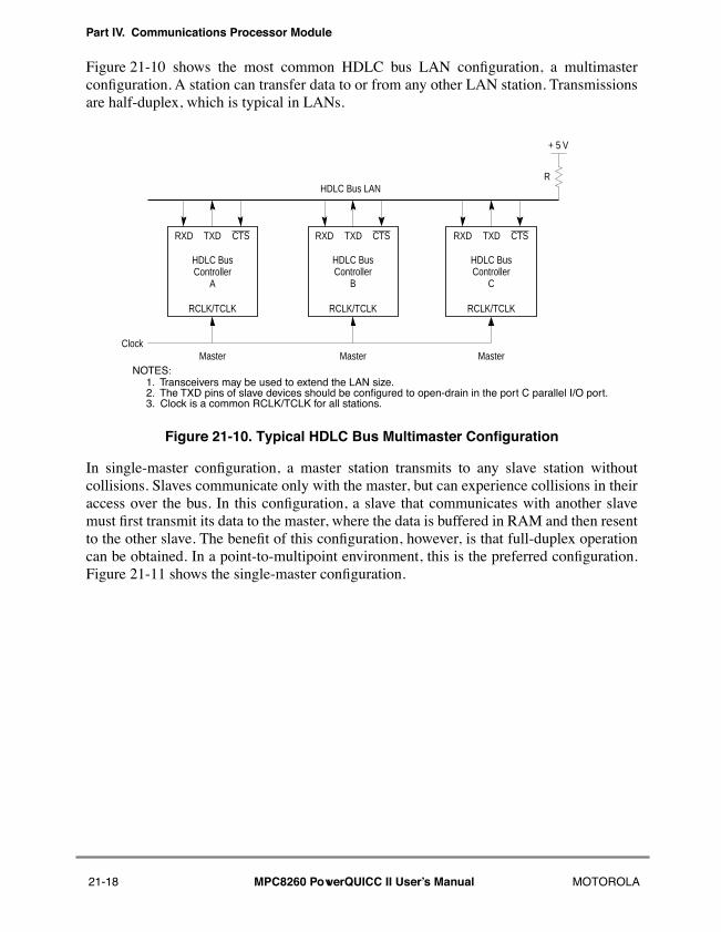
Part IV. Communications Processor Module
Figure 21-10 shows the most common HDLC bus LAN conÞguration, a multimasterconÞguration. A station can transfer data to or from any other LAN station. Transmissionsare half-duplex, which is typical in LANs.
Figure 21-10. Typical HDLC Bus Multimaster Configuration
In single-master conÞguration, a master station transmits to any slave station withoutcollisions. Slaves communicate only with the master, but can experience collisions in theiraccess over the bus. In this conÞguration, a slave that communicates with another slavemust Þrst transmit its data to the master, where the data is buffered in RAM and then resentto the other slave. The beneÞt of this conÞguration, however, is that full-duplex operationcan be obtained. In a point-to-multipoint environment, this is the preferred conÞguration.Figure 21-11 shows the single-master conÞguration.
HDLC BusController
RXD CTSTXD
A
RCLK/TCLK
HDLC BusController
RXD CTSTXD
B
RCLK/TCLK
HDLC BusController
RXD CTSTXD
C
RCLK/TCLK
Clock
HDLC Bus LAN
+ 5 V
R
Master MasterMasterNOTES:
1. Transceivers may be used to extend the LAN size.2. The TXD pins of slave devices should be configured to open-drain in the port C parallel I/O port.3. Clock is a common RCLK/TCLK for all stations.
21-18 MPC8260 PowerQUICC II UserÕs Manual MOTOROLA
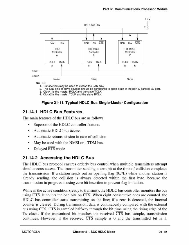
Part IV. Communications Processor Module
Figure 21-11. Typical HDLC Bus Single-Master Configuration
21.14.1 HDLC Bus FeaturesThe main features of the HDLC bus are as follows:
¥ Superset of the HDLC controller features
¥ Automatic HDLC bus access
¥ Automatic retransmission in case of collision
¥ May be used with the NMSI or a TDM bus
¥ Delayed RTS mode
21.14.2 Accessing the HDLC BusThe HDLC bus protocol ensures orderly bus control when multiple transmitters attemptsimultaneous access. The transmitter sending a zero bit at the time of collision completesthe transmission. If a station sends out an opening ßag (0x7E) while another station isalready sending, the collision is always detected within the Þrst byte, because thetransmission in progress is using zero bit insertion to prevent ßag imitation.
While in the active condition (ready to transmit), the HDLC bus controller monitors the bususing CTS. It counts the one bits on CTS. When eight consecutive ones are counted, theHDLC bus controller starts transmitting on the line; if a zero is detected, the internalcounter is cleared. During transmission, data is continuously compared with the externalbus using CTS. CTS is sampled halfway through the bit time using the rising edge of theTx clock. If the transmitted bit matches the received CTS bus sample, transmissioncontinues. However, if the received CTS sample is 0 and the transmitted bit is 1,
HDLCController
RXD TXD
A
RCLK
HDLC BusController
RXD CTSTXD
B
HDLC BusController
RXD CTSTXD
C
Clock1
HDLC Bus LAN
+ 5 V
R
Slave SlaveMasterNOTES:
1. Transceivers may be used to extend the LAN size.2. The TXD pins of slave devices should be configured to open-drain in the port C parallel I/O port.3. Clock1 is the master RCLK and the slave TCLK.
Clock2
TCLK RCLK TCLKRCLK TCLK
4. Clock2 is the master TCLK and the slave RCLK.
MOTOROLA Chapter 21. SCC HDLC Mode 21-19
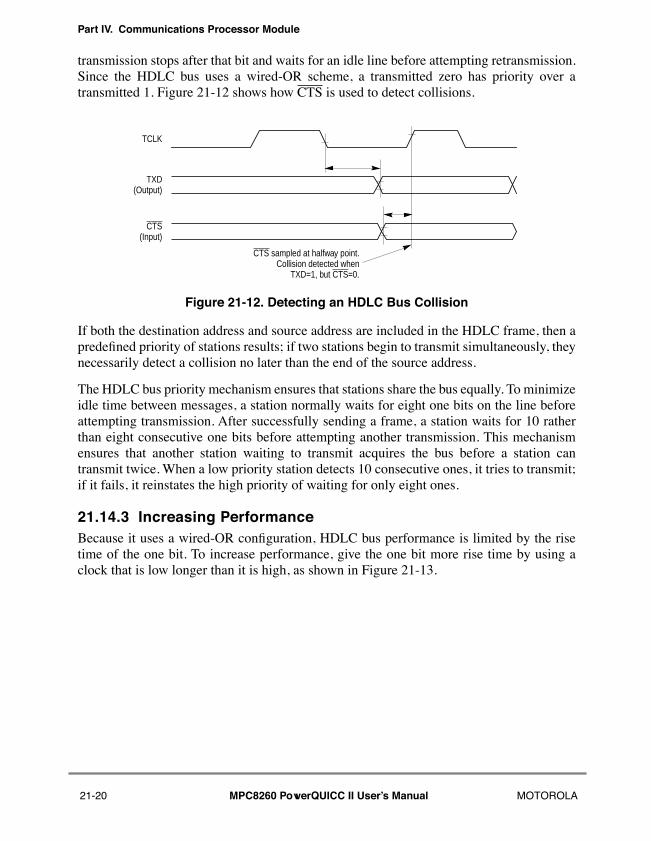
Part IV. Communications Processor Module
transmission stops after that bit and waits for an idle line before attempting retransmission.Since the HDLC bus uses a wired-OR scheme, a transmitted zero has priority over atransmitted 1. Figure 21-12 shows how CTS is used to detect collisions.
Figure 21-12. Detecting an HDLC Bus Collision
If both the destination address and source address are included in the HDLC frame, then apredeÞned priority of stations results; if two stations begin to transmit simultaneously, theynecessarily detect a collision no later than the end of the source address.
The HDLC bus priority mechanism ensures that stations share the bus equally. To minimizeidle time between messages, a station normally waits for eight one bits on the line beforeattempting transmission. After successfully sending a frame, a station waits for 10 ratherthan eight consecutive one bits before attempting another transmission. This mechanismensures that another station waiting to transmit acquires the bus before a station cantransmit twice. When a low priority station detects 10 consecutive ones, it tries to transmit;if it fails, it reinstates the high priority of waiting for only eight ones.
21.14.3 Increasing PerformanceBecause it uses a wired-OR conÞguration, HDLC bus performance is limited by the risetime of the one bit. To increase performance, give the one bit more rise time by using aclock that is low longer than it is high, as shown in Figure 21-13.
TCLK
CTS(Input)
TXD(Output)
CTS sampled at halfway point.Collision detected when
TXD=1, but CTS=0.
21-20 MPC8260 PowerQUICC II UserÕs Manual MOTOROLA
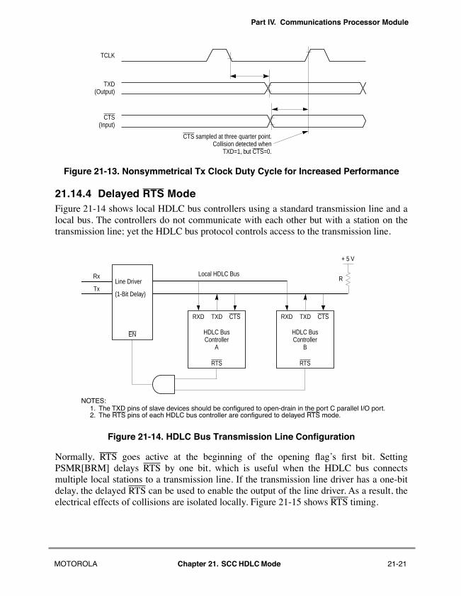
Part IV. Communications Processor Module
Figure 21-13. Nonsymmetrical Tx Clock Duty Cycle for Increased Performance
21.14.4 Delayed RTS Mode Figure 21-14 shows local HDLC bus controllers using a standard transmission line and alocal bus. The controllers do not communicate with each other but with a station on thetransmission line; yet the HDLC bus protocol controls access to the transmission line.
Figure 21-14. HDLC Bus Transmission Line Configuration
Normally, RTS goes active at the beginning of the opening ßagÕs Þrst bit. SettingPSMR[BRM] delays RTS by one bit, which is useful when the HDLC bus connectsmultiple local stations to a transmission line. If the transmission line driver has a one-bitdelay, the delayed RTS can be used to enable the output of the line driver. As a result, theelectrical effects of collisions are isolated locally. Figure 21-15 shows RTS timing.
TCLK
CTS(Input)
TXD(Output)
CTS sampled at three quarter point.Collision detected when
TXD=1, but CTS=0.
Local HDLC Bus
HDLC BusController
RXD CTSTXD
A
HDLC BusController
RXD CTSTXD
B
RTS
+ 5 V
R
NOTES:1. The TXD pins of slave devices should be configured to open-drain in the port C parallel I/O port.2. The RTS pins of each HDLC bus controller are configured to delayed RTS mode.
RTS
Tx
Rx
EN
(1-Bit Delay)
Line Driver
MOTOROLA Chapter 21. SCC HDLC Mode 21-21
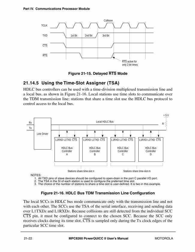
Part IV. Communications Processor Module
Figure 21-15. Delayed RTS Mode
21.14.5 Using the Time-Slot Assigner (TSA)HDLC bus controllers can be used with a time-division multiplexed transmission line anda local bus, as shown in Figure 21-16. Local stations use time slots to communicate overthe TDM transmission line; stations that share a time slot use the HDLC bus protocol tocontrol access to the local bus.
Figure 21-16. HDLC Bus TDM Transmission Line Configuration
The local SCCs in HDLC bus mode communicate only with the transmission line and notwith each other. The SCCs use the TSA of the serial interface, receiving and sending dataover L1TXDx and L1RXDx. Because collisions are still detected from the individual SCCCTS pin, it must be conÞgured to connect to the chosen SCC. Because the SCC onlyreceives clocks during its time slot, CTS is sampled only during the Tx clock edges of theparticular SCC time slot.
TCLK
RTS active foronly 2 bit times
TXD
CTS
RTS
1st Bit 2nd Bit 3rd Bit
Collision
Local HDLC Bus
HDLC BusController
L1RXD CTSL1TXD
B
HDLC BusController
L1RXD CTSL1TXD
D
+ 5 V
R
NOTES:1. All TXD pins of slave devices should be configured to open-drain in the port C parallel I/O port.2. The TSA in the SI of each station is used to configure the preferred time slot.
Tx
Rx
Line Driver
HDLC BusController
L1RXD CTSL1TXD
C
HDLC BusController
L1RXD CTSL1TXD
A
Stations share time-slot n Stations share time-slot m
3. The choice of the number of stations to share a time slot is user-defined. It is two in this example.
21-22 MPC8260 PowerQUICC II UserÕs Manual MOTOROLA
Part IV. Communications Processor Module
21.14.6 HDLC Bus Protocol ProgrammingThe HDLC bus on the MPC8260 is implemented using the SCC in HDLC mode with bus-speciÞc options selected in the PSMR and GSMR, as outlined below. See also Section 21.5,ÒProgramming the SCC in HDLC Mode.Ó
21.14.6.1 Programming GSMR and PSMR for the HDLC Bus ProtocolTo program the protocol-speciÞc mode register (PSMR), set the bits as described below:
¥ ConÞgure NOF as preferred
¥ Set RTE and BUS to 1
¥ Set BRM to 1 if delayed RTS is desired
¥ ConÞgure CRC to 16-bit CRC CCITT (0b00).
¥ ConÞgure other bits to zero or default.
To program the general SCC mode register (GSMR), set the bits as described below:
¥ Set MODE to HDLC mode (0b0000).
¥ ConÞgure CTSS to 1 and all other bits to zero or default.
¥ ConÞgure the DIAG bits for normal operation (0b00).
¥ ConÞgure RDCR and TDCR for 1´ clock (0b00).
¥ ConÞgure TENC and RENC for NRZ (0b000).
¥ Clear RTSM to send idles between frames.
¥ Set GSMR_L[ENT, ENR] as the last step to begin operation.
21.14.6.2 HDLC Bus Controller Programming ExampleExcept for the above discussion in Section 21.14.6.1, ÒProgramming GSMR and PSMR forthe HDLC Bus Protocol,Ó use the example in Section 21.13.1, ÒSCC HDLC ProgrammingExample #1.Ó
MOTOROLA Chapter 21. SCC HDLC Mode 21-23

Part IV. Communications Processor Module
21-24 MPC8260 PowerQUICC II UserÕs Manual MOTOROLA
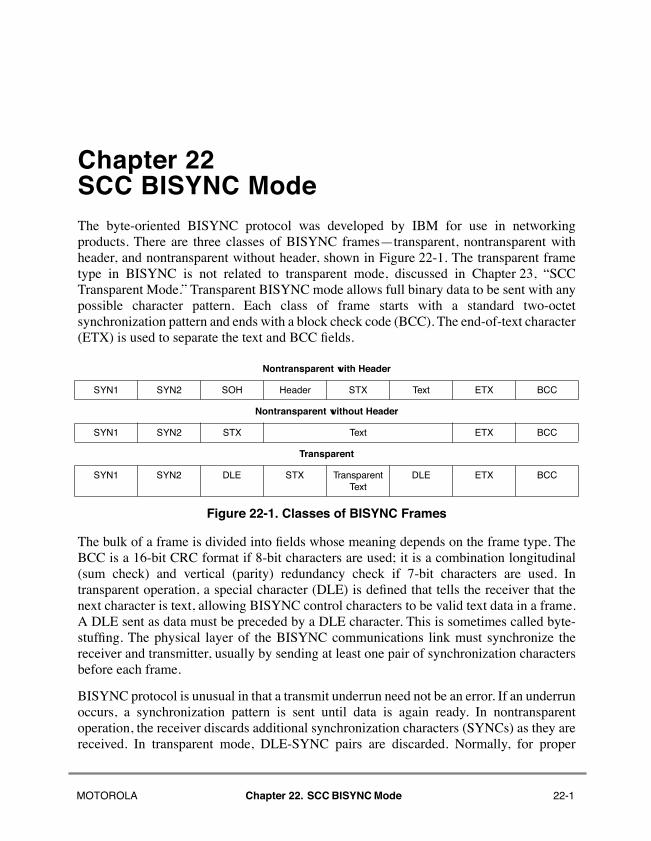
Chapter 22 SCC BISYNC Mode220220
The byte-oriented BISYNC protocol was developed by IBM for use in networkingproducts. There are three classes of BISYNC framesÑtransparent, nontransparent withheader, and nontransparent without header, shown in Figure 22-1. The transparent frametype in BISYNC is not related to transparent mode, discussed in Chapter 23, ÒSCCTransparent Mode.Ó Transparent BISYNC mode allows full binary data to be sent with anypossible character pattern. Each class of frame starts with a standard two-octetsynchronization pattern and ends with a block check code (BCC). The end-of-text character(ETX) is used to separate the text and BCC Þelds.
Figure 22-1. Classes of BISYNC Frames
The bulk of a frame is divided into Þelds whose meaning depends on the frame type. TheBCC is a 16-bit CRC format if 8-bit characters are used; it is a combination longitudinal(sum check) and vertical (parity) redundancy check if 7-bit characters are used. Intransparent operation, a special character (DLE) is deÞned that tells the receiver that thenext character is text, allowing BISYNC control characters to be valid text data in a frame.A DLE sent as data must be preceded by a DLE character. This is sometimes called byte-stufÞng. The physical layer of the BISYNC communications link must synchronize thereceiver and transmitter, usually by sending at least one pair of synchronization charactersbefore each frame.
BISYNC protocol is unusual in that a transmit underrun need not be an error. If an underrunoccurs, a synchronization pattern is sent until data is again ready. In nontransparentoperation, the receiver discards additional synchronization characters (SYNCs) as they arereceived. In transparent mode, DLE-SYNC pairs are discarded. Normally, for proper
Nontransparent with Header
SYN1 SYN2 SOH Header STX Text ETX BCC
Nontransparent without Header
SYN1 SYN2 STX Text ETX BCC
Transparent
SYN1 SYN2 DLE STX Transparent Text
DLE ETX BCC
MOTOROLA Chapter 22. SCC BISYNC Mode 22-1
Part IV. Communications Processor Module
transmission, an underrun must not occur between the DLE and its following character.This failure mode cannot occur with the MPC8260.
An SCC can be conÞgured as a BISYNC controller to handle basic BISYNC protocol innormal and transparent modes. The controller can work with the time-slot assigner (TSA)or nonmultiplexed serial interface (NMSI). The controller has separate transmit and receivesections whose operations are asynchronous with the core and either synchronous orasynchronous with other SCCs.
22.1 FeaturesThe following list summarizes features of the SCC in BISYNC mode:
¥ Flexible data buffers¥ Eight control character recognition registers¥ Automatic SYNC1ÐSYNC2 detection¥ 16-bit pattern (bisync)¥ 8-bit pattern (monosync)¥ 4-bit pattern (nibblesync)¥ External SYNC pin support¥ SYNC/DLE stripping and insertion¥ CRC16 and LRC (sum check) generation/checking¥ VRC (parity) generation/checking¥ Supports BISYNC transparent operation ¥ Maintains parity error counter¥ Reverse data mode capability
22.2 SCC BISYNC Channel Frame TransmissionThe BISYNC transmitter is designed to work with almost no core intervention. When thetransmitter is enabled, it starts sending SYN1ÐSYN2 pairs in the data synchronizationregister (DSR) or idles as programmed in the PSMR. The BISYNC controller polls the ÞrstBD in the channelÕs TxBD table. If there is a message to send, the controller fetches themessage from memory and starts sending it after the SYN1ÐSYN2 pair. The entire pair isalways sent, regardless of GSMR[SYNL].
After a buffer is sent, if the last (TxBD[L]) and the Tx block check sequence (TxBD[TB])bits are set, the BISYNC controller appends the CRC16/LRC and then writes the messagestatus bits in TxBD status and control Þelds and clears the ready bit, TxBD[R]. It then startssending the SYN1ÐSYN2 pairs or idles, according to GSMR[RTSM]. If the end of thecurrent BD is reached and TxBD[L] is not set, only TxBD[R] is cleared. In both cases, aninterrupt is issued according to TxBD[I]. TxBD[I] controls whether interrupts are generatedafter transmission of each buffer, a speciÞc buffer, or each block. The controller thenproceeds to the next BD.
22-2 MPC8260 PowerQUICC II UserÕs Manual MOTOROLA
Part IV. Communications Processor Module
If no additional buffers have been sent to the controller for transmission, an in-frameunderrun is detected and the controller starts sending syncs or idles. If the controller is intransparent mode, it sends DLE-sync pairs. Characters are included in the block checksequence (BCS) calculation on a per-buffer basis. Each buffer can be programmedindependently to be included or excluded from the BCS calculation; thus, excludedcharacters must reside in a separate buffer. The controller can reset the BCS generatorbefore sending a speciÞc buffer. In transparent mode, the controller inserts a DLE beforesending a DLE character, so that only one DLE is used in the calculation.
22.3 SCC BISYNC Channel Frame ReceptionAlthough the receiver is designed to work with almost no core intervention, the user canintervene on a per-byte basis if necessary. The receiver performs CRC16, longitudinal(LRC) or vertical redundancy (VRC) checking, sync stripping in normal mode, DLE-syncstripping, stripping of the Þrst DLE in DLE-DLE pairs in transparent mode, and controlcharacter recognition. Control characters are discussed in Section 22.6, ÒSCC BISYNCControl Character Recognition.Ó
When enabled, the receiver enters hunt mode where the data is shifted into the receiver shiftregister one bit at a time and the contents of the shift register are compared to the contentsof DSR[SYN1, SYN2]. If the two are unequal, the next bit is shifted in and the comparisonis repeated. When registers match, hunt mode is terminated and character assembly begins.The controller is character-synchronized and performs SYNC stripping and messagereception. It reverts to hunt mode when it receives an ENTER HUNT MODE command, an errorcondition, or an appropriate control character.
When receiving data, the controller updates the BCS bit in the BD for each byte transferred.When the buffer is full, the controller clears the E bit in the BD and generates an interruptif the I bit in the BD is set. If incoming data exceeds the buffer length, the controller fetchesthe next BD; if E is zero, reception continues to its buffer.
When a BCS is received, it is checked and written to the buffer. The BISYNC controllersets the last bit, writes the message status bits into the BD, clears the E bit, and thengenerates a maskable interrupt, indicating that a block of data was received and is inmemory. The BCS calculations do not include SYNCs (in nontransparent mode) or DLE-SYNC pairs (in transparent mode).
Note that GSMR_H[RFW] should be set for an 8-bit-wide receive FIFO for the BISYNCreceiver. See Section 19.1.1, ÒThe General SCC Mode Registers (GSMR1ÐGSMR4).Ó
22.4 SCC BISYNC Parameter RAMFor BISYNC mode, the protocol-speciÞc area of the SCC parameter RAM is mapped as inTable 22-1.
MOTOROLA Chapter 22. SCC BISYNC Mode 22-3
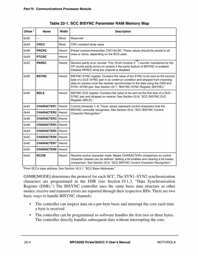
Part IV. Communications Processor Module
GSMR[MODE] determines the protocol for each SCC. The SYN1ÐSYN2 synchronizationcharacters are programmed in the DSR (see Section 19.1.3, ÒData SynchronizationRegister (DSR).Ó) The BISYNC controller uses the same basic data structure as othermodes; receive and transmit errors are reported through their respective BDs. There are twobasic ways to handle BISYNC channels:
¥ The controller can inspect data on a per-byte basis and interrupt the core each time a byte is received.
¥ The controller can be programmed so software handles the Þrst two or three bytes. The controller directly handles subsequent data without interrupting the core.
Table 22-1. SCC BISYNC Parameter RAM Memory Map
Offset 1
1From SCCx base address. See Section 19.3.1, ÒSCC Base Addresses.Ó
Name Width Description
0x30 Ñ Word Reserved
0x34 CRCC Word CRC constant temp value.
0x38 PRCRC Hword Preset receiver/transmitter CRC16/LRC. These values should be preset to all ones or zeros, depending on the BCS used.
0x3A PTCRC Hword
0x3C PAREC Hword Receive parity error counter. This 16-bit (modulo 216
) counter maintained by the CP counts parity errors on receive if the parity feature of BISYNC is enabled. Initialize PAREC while the channel is disabled.
0x3E BSYNC Hword BISYNC SYNC register. Contains the value of the SYNC to be sent as the second byte of a DLEÐSYNC pair in an underrun condition and stripped from incoming data on receive once the receiver synchronizes to the data using the DSR and SYN1ÐSYN2 pair. See Section 22.7, ÒBISYNC SYNC Register (BSYNC).Ó
0x40 BDLE Hword BISYNC DLE register. Contains the value to be sent as the Þrst byte of a DLEÐSYNC pair and stripped on receive. See Section 22.8, ÒSCC BISYNC DLE Register (BDLE).Ó
0x42 CHARACTER1 Hword Control character 1Ð8. These values represent control characters that the BISYNC controller recognizes. See Section 22.6, ÒSCC BISYNC Control Character Recognition.Ó0x44 CHARACTER2 Hword
0x46 CHARACTER3 Hword
0x48 CHARACTER4 Hword
0x4A CHARACTER5 Hword
0x4C CHARACTER6 Hword
0x4E CHARACTER7 Hword
0x50 CHARACTER8 Hword
0x52 RCCM Hword Receive control character mask. Masks CHARACTERn comparison so control character classes can be deÞned. Setting a bit enables and clearing a bit masks comparison. See Section 22.6, ÒSCC BISYNC Control Character Recognition.Ó
22-4 MPC8260 PowerQUICC II UserÕs Manual MOTOROLA
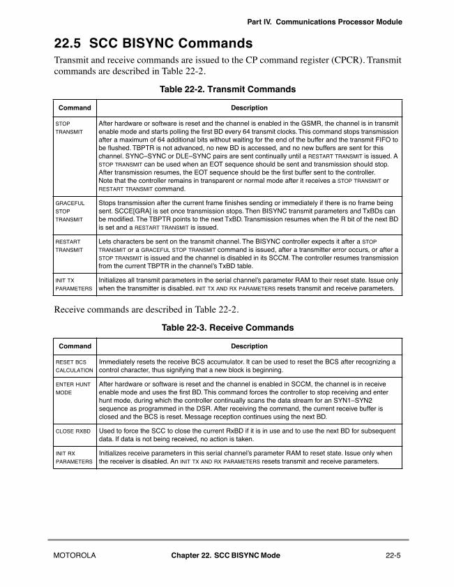
Part IV. Communications Processor Module
22.5 SCC BISYNC CommandsTransmit and receive commands are issued to the CP command register (CPCR). Transmitcommands are described in Table 22-2.
Receive commands are described in Table 22-2.
Table 22-2. Transmit Commands
Command Description
STOP TRANSMIT
After hardware or software is reset and the channel is enabled in the GSMR, the channel is in transmit enable mode and starts polling the Þrst BD every 64 transmit clocks. This command stops transmission after a maximum of 64 additional bits without waiting for the end of the buffer and the transmit FIFO to be ßushed. TBPTR is not advanced, no new BD is accessed, and no new buffers are sent for this channel. SYNCÐSYNC or DLEÐSYNC pairs are sent continually until a RESTART TRANSMIT is issued. A STOP TRANSMIT can be used when an EOT sequence should be sent and transmission should stop. After transmission resumes, the EOT sequence should be the Þrst buffer sent to the controller.Note that the controller remains in transparent or normal mode after it receives a STOP TRANSMIT or RESTART TRANSMIT command.
GRACEFUL STOP TRANSMIT
Stops transmission after the current frame Þnishes sending or immediately if there is no frame being sent. SCCE[GRA] is set once transmission stops. Then BISYNC transmit parameters and TxBDs can be modiÞed. The TBPTR points to the next TxBD. Transmission resumes when the R bit of the next BD is set and a RESTART TRANSMIT is issued.
RESTART TRANSMIT
Lets characters be sent on the transmit channel. The BISYNC controller expects it after a STOP TRANSMIT or a GRACEFUL STOP TRANSMIT command is issued, after a transmitter error occurs, or after a STOP TRANSMIT is issued and the channel is disabled in its SCCM. The controller resumes transmission from the current TBPTR in the channelÕs TxBD table.
INIT TX PARAMETERS
Initializes all transmit parameters in the serial channelÕs parameter RAM to their reset state. Issue only when the transmitter is disabled. INIT TX AND RX PARAMETERS resets transmit and receive parameters.
Table 22-3. Receive Commands
Command Description
RESET BCS CALCULATION
Immediately resets the receive BCS accumulator. It can be used to reset the BCS after recognizing a control character, thus signifying that a new block is beginning.
ENTER HUNT MODE
After hardware or software is reset and the channel is enabled in SCCM, the channel is in receive enable mode and uses the Þrst BD. This command forces the controller to stop receiving and enter hunt mode, during which the controller continually scans the data stream for an SYN1ÐSYN2 sequence as programmed in the DSR. After receiving the command, the current receive buffer is closed and the BCS is reset. Message reception continues using the next BD.
CLOSE RXBD Used to force the SCC to close the current RxBD if it is in use and to use the next BD for subsequent data. If data is not being received, no action is taken.
INIT RX PARAMETERS
Initializes receive parameters in this serial channelÕs parameter RAM to reset state. Issue only when the receiver is disabled. An INIT TX AND RX PARAMETERS resets transmit and receive parameters.
MOTOROLA Chapter 22. SCC BISYNC Mode 22-5
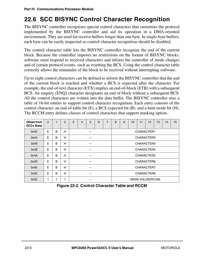
Part IV. Communications Processor Module
22.6 SCC BISYNC Control Character RecognitionThe BISYNC controller recognizes special control characters that customize the protocolimplemented by the BISYNC controller and aid its operation in a DMA-orientedenvironment. They are used for receive buffers longer than one byte. In single-byte buffers,each byte can be easily inspected so control character recognition should be disabled.
The control character table lets the BISYNC controller recognize the end of the currentblock. Because the controller imposes no restrictions on the format of BISYNC blocks,software must respond to received characters and inform the controller of mode changesand of certain protocol events, such as resetting the BCS. Using the control character tablecorrectly allows the remainder of the block to be received without interrupting software.
Up to eight control characters can be deÞned to inform the BISYNC controller that the endof the current block is reached and whether a BCS is expected after the character. Forexample, the end-of-text character (ETX) implies an end-of-block (ETB) with a subsequentBCS. An enquiry (ENQ) character designates an end of block without a subsequent BCS.All the control characters are written into the data buffer. The BISYNC controller uses atable of 16-bit entries to support control character recognition. Each entry consists of thecontrol character, an end-of-table bit (E), a BCS expected bit (B), and a hunt mode bit (H).The RCCM entry deÞnes classes of control characters that support masking option.
Offset from SCCx Base
0 1 2 3 4 5 6 7 8 9 10 11 12 13 14 15
0x42 E B H Ñ CHARACTER1
0x44 E B H Ñ CHARACTER2
0x46 E B H Ñ CHARACTER3
0x48 E B H Ñ CHARACTER4
0x4A E B H Ñ CHARACTER5
0x4D E B H Ñ CHARACTER6
0x4E E B H Ñ CHARACTER7
0x50 E B H Ñ CHARACTER8
0x52 1 1 1 Ñ MASK VALUE(RCCM)
Figure 22-2. Control Character Table and RCCM
22-6 MPC8260 PowerQUICC II UserÕs Manual MOTOROLA
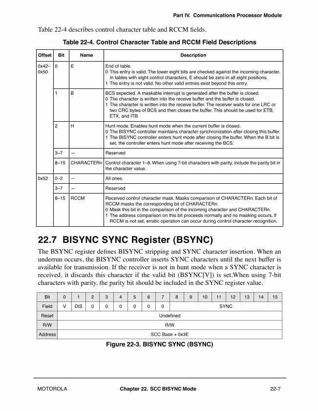
Part IV. Communications Processor Module
Table 22-4 describes control character table and RCCM Þelds.
22.7 BISYNC SYNC Register (BSYNC)The BSYNC register deÞnes BISYNC stripping and SYNC character insertion. When anunderrun occurs, the BISYNC controller inserts SYNC characters until the next buffer isavailable for transmission. If the receiver is not in hunt mode when a SYNC character isreceived, it discards this character if the valid bit (BSYNC[V]) is set.When using 7-bitcharacters with parity, the parity bit should be included in the SYNC register value.
Table 22-4. Control Character Table and RCCM Field Descriptions
Offset Bit Name Description
0x42Ð0x50
0 E End of table. 0 This entry is valid. The lower eight bits are checked against the incoming character.
In tables with eight control characters, E should be zero in all eight positions. 1 The entry is not valid. No other valid entries exist beyond this entry.
1 B BCS expected. A maskable interrupt is generated after the buffer is closed.0 The character is written into the receive buffer and the buffer is closed. 1 The character is written into the receive buffer. The receiver waits for one LRC or
two CRC bytes of BCS and then closes the buffer. This should be used for ETB, ETX, and ITB.
2 H Hunt mode. Enables hunt mode when the current buffer is closed.0 The BISYNC controller maintains character synchronization after closing this buffer. 1 The BISYNC controller enters hunt mode after closing the buffer. When the B bit is
set, the controller enters hunt mode after receiving the BCS.
3Ð7 Ñ Reserved
8Ð15 CHARACTERn Control character 1Ð8. When using 7-bit characters with parity, include the parity bit in the character value.
0x52 0Ð2 Ñ All ones.
3Ð7 Ñ Reserved
8Ð15 RCCM Received control character mask. Masks comparison of CHARACTERn. Each bit of RCCM masks the corresponding bit of CHARACTERn. 0 Mask this bit in the comparison of the incoming character and CHARACTERn.1 The address comparison on this bit proceeds normally and no masking occurs. If
RCCM is not set, erratic operation can occur during control character recognition.
Bit 0 1 2 3 4 5 6 7 8 9 10 11 12 13 14 15
Field V DIS 0 0 0 0 0 0 SYNC
Reset UndeÞned
R/W R/W
Address SCC Base + 0x3E
Figure 22-3. BISYNC SYNC (BSYNC)
MOTOROLA Chapter 22. SCC BISYNC Mode 22-7
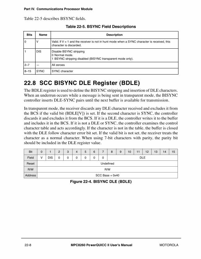
Part IV. Communications Processor Module
Table 22-5 describes BSYNC Þelds.
22.8 SCC BISYNC DLE Register (BDLE)The BDLE register is used to deÞne the BISYNC stripping and insertion of DLE characters.When an underrun occurs while a message is being sent in transparent mode, the BISYNCcontroller inserts DLE-SYNC pairs until the next buffer is available for transmission.
In transparent mode, the receiver discards any DLE character received and excludes it fromthe BCS if the valid bit (BDLE[V]) is set. If the second character is SYNC, the controllerdiscards it and excludes it from the BCS. If it is a DLE, the controller writes it to the bufferand includes it in the BCS. If it is not a DLE or SYNC, the controller examines the controlcharacter table and acts accordingly. If the character is not in the table, the buffer is closedwith the DLE follow character error bit set. If the valid bit is not set, the receiver treats thecharacter as a normal character. When using 7-bit characters with parity, the parity bitshould be included in the DLE register value.
Table 22-5. BSYNC Field Descriptions
Bits Name Description
0 V Valid. If V = 1 and the receiver is not in hunt mode when a SYNC character is received, this character is discarded.
1 DIS Disable BSYNC stripping0 Normal mode.1 BSYNC stripping disabled (BISYNC transparent mode only).
2Ð7 Ñ All zeroes
8Ð15 SYNC SYNC character
Bit 0 1 2 3 4 5 6 7 8 9 10 11 12 13 14 15
Field V DIS 0 0 0 0 0 0 DLE
Reset UndeÞned
R/W R/W
Address SCC Base + 0x40
Figure 22-4. BISYNC DLE (BDLE)
22-8 MPC8260 PowerQUICC II UserÕs Manual MOTOROLA
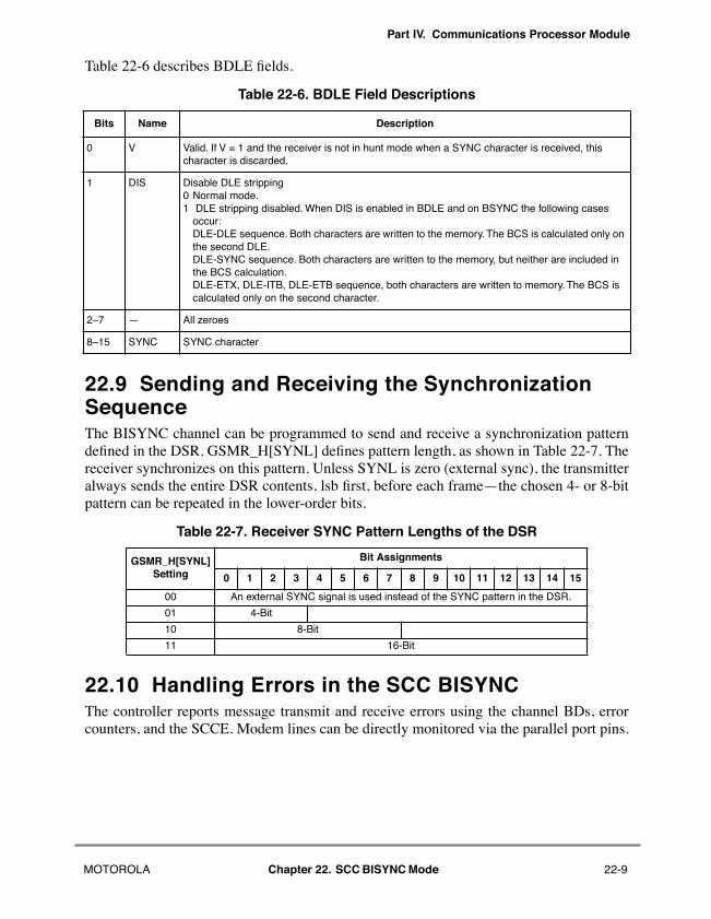
Part IV. Communications Processor Module
Table 22-6 describes BDLE Þelds.
22.9 Sending and Receiving the Synchronization SequenceThe BISYNC channel can be programmed to send and receive a synchronization patterndeÞned in the DSR. GSMR_H[SYNL] deÞnes pattern length, as shown in Table 22-7. Thereceiver synchronizes on this pattern. Unless SYNL is zero (external sync), the transmitteralways sends the entire DSR contents, lsb Þrst, before each frameÑthe chosen 4- or 8-bitpattern can be repeated in the lower-order bits.
22.10 Handling Errors in the SCC BISYNCThe controller reports message transmit and receive errors using the channel BDs, errorcounters, and the SCCE. Modem lines can be directly monitored via the parallel port pins.
Table 22-6. BDLE Field Descriptions
Bits Name Description
0 V Valid. If V = 1 and the receiver is not in hunt mode when a SYNC character is received, this character is discarded.
1 DIS Disable DLE stripping0 Normal mode.1 DLE stripping disabled. When DIS is enabled in BDLE and on BSYNC the following cases
occur:DLE-DLE sequence. Both characters are written to the memory. The BCS is calculated only on the second DLE.DLE-SYNC sequence. Both characters are written to the memory, but neither are included in the BCS calculation.DLE-ETX, DLE-ITB, DLE-ETB sequence, both characters are written to memory. The BCS is calculated only on the second character.
2Ð7 Ñ All zeroes
8Ð15 SYNC SYNC character
Table 22-7. Receiver SYNC Pattern Lengths of the DSR
GSMR_H[SYNL] Setting
Bit Assignments
0 1 2 3 4 5 6 7 8 9 10 11 12 13 14 15
00 An external SYNC signal is used instead of the SYNC pattern in the DSR.
01 4-Bit
10 8-Bit
11 16-Bit
MOTOROLA Chapter 22. SCC BISYNC Mode 22-9
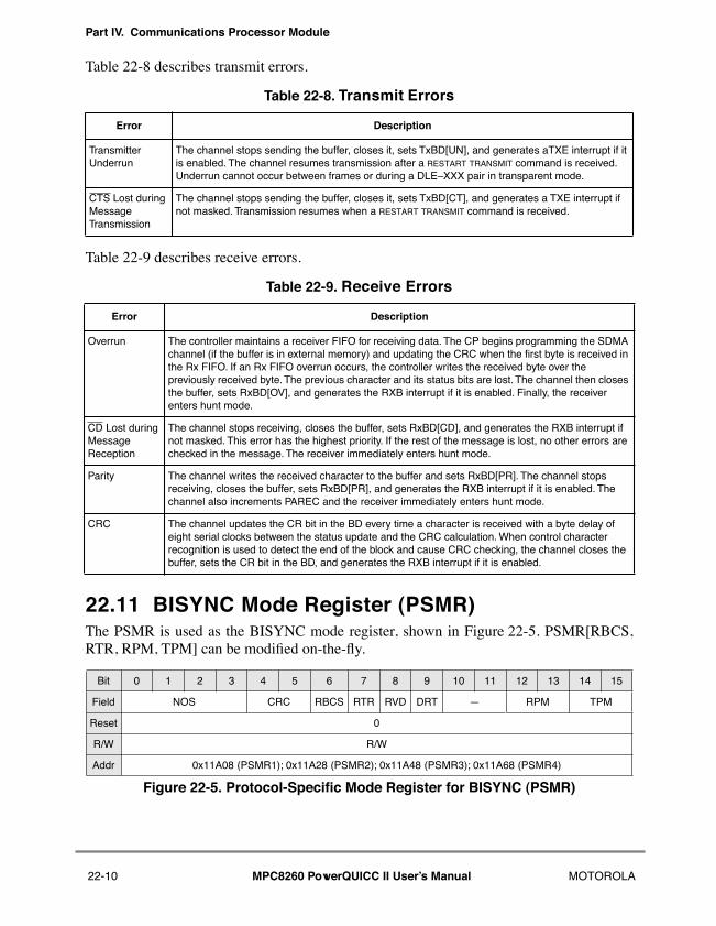
Part IV. Communications Processor Module
Table 22-8 describes transmit errors.
Table 22-9 describes receive errors.
22.11 BISYNC Mode Register (PSMR) The PSMR is used as the BISYNC mode register, shown in Figure 22-5. PSMR[RBCS,RTR, RPM, TPM] can be modiÞed on-the-ßy.
Table 22-8. Transmit Errors
Error Description
Transmitter Underrun
The channel stops sending the buffer, closes it, sets TxBD[UN], and generates aTXE interrupt if it is enabled. The channel resumes transmission after a RESTART TRANSMIT command is received. Underrun cannot occur between frames or during a DLEÐXXX pair in transparent mode.
CTS Lost during Message Transmission
The channel stops sending the buffer, closes it, sets TxBD[CT], and generates a TXE interrupt if not masked. Transmission resumes when a RESTART TRANSMIT command is received.
Table 22-9. Receive Errors
Error Description
Overrun The controller maintains a receiver FIFO for receiving data. The CP begins programming the SDMA channel (if the buffer is in external memory) and updating the CRC when the Þrst byte is received in the Rx FIFO. If an Rx FIFO overrun occurs, the controller writes the received byte over the previously received byte. The previous character and its status bits are lost. The channel then closes the buffer, sets RxBD[OV], and generates the RXB interrupt if it is enabled. Finally, the receiver enters hunt mode.
CD Lost during Message Reception
The channel stops receiving, closes the buffer, sets RxBD[CD], and generates the RXB interrupt if not masked. This error has the highest priority. If the rest of the message is lost, no other errors are checked in the message. The receiver immediately enters hunt mode.
Parity The channel writes the received character to the buffer and sets RxBD[PR]. The channel stops receiving, closes the buffer, sets RxBD[PR], and generates the RXB interrupt if it is enabled. The channel also increments PAREC and the receiver immediately enters hunt mode.
CRC The channel updates the CR bit in the BD every time a character is received with a byte delay of eight serial clocks between the status update and the CRC calculation. When control character recognition is used to detect the end of the block and cause CRC checking, the channel closes the buffer, sets the CR bit in the BD, and generates the RXB interrupt if it is enabled.
Bit 0 1 2 3 4 5 6 7 8 9 10 11 12 13 14 15
Field NOS CRC RBCS RTR RVD DRT Ñ RPM TPM
Reset 0
R/W R/W
Addr 0x11A08 (PSMR1); 0x11A28 (PSMR2); 0x11A48 (PSMR3); 0x11A68 (PSMR4)
Figure 22-5. Protocol-Specific Mode Register for BISYNC (PSMR)
22-10 MPC8260 PowerQUICC II UserÕs Manual MOTOROLA
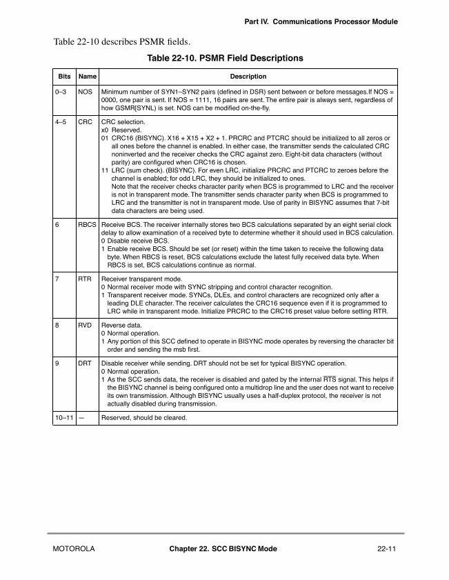
Part IV. Communications Processor Module
Table 22-10 describes PSMR Þelds.
Table 22-10. PSMR Field Descriptions
Bits Name Description
0Ð3 NOS Minimum number of SYN1ÐSYN2 pairs (deÞned in DSR) sent between or before messages.If NOS = 0000, one pair is sent. If NOS = 1111, 16 pairs are sent. The entire pair is always sent, regardless of how GSMR[SYNL) is set. NOS can be modiÞed on-the-ßy.
4Ð5 CRC CRC selection. x0 Reserved.01 CRC16 (BISYNC). X16 + X15 + X2 + 1. PRCRC and PTCRC should be initialized to all zeros or
all ones before the channel is enabled. In either case, the transmitter sends the calculated CRC noninverted and the receiver checks the CRC against zero. Eight-bit data characters (without parity) are conÞgured when CRC16 is chosen.
11 LRC (sum check). (BISYNC). For even LRC, initialize PRCRC and PTCRC to zeroes before the channel is enabled; for odd LRC, they should be initialized to ones.Note that the receiver checks character parity when BCS is programmed to LRC and the receiver is not in transparent mode. The transmitter sends character parity when BCS is programmed to LRC and the transmitter is not in transparent mode. Use of parity in BISYNC assumes that 7-bit data characters are being used.
6 RBCS Receive BCS. The receiver internally stores two BCS calculations separated by an eight serial clock delay to allow examination of a received byte to determine whether it should used in BCS calculation. 0 Disable receive BCS.1 Enable receive BCS. Should be set (or reset) within the time taken to receive the following data
byte. When RBCS is reset, BCS calculations exclude the latest fully received data byte. When RBCS is set, BCS calculations continue as normal.
7 RTR Receiver transparent mode. 0 Normal receiver mode with SYNC stripping and control character recognition. 1 Transparent receiver mode. SYNCs, DLEs, and control characters are recognized only after a
leading DLE character. The receiver calculates the CRC16 sequence even if it is programmed to LRC while in transparent mode. Initialize PRCRC to the CRC16 preset value before setting RTR.
8 RVD Reverse data. 0 Normal operation. 1 Any portion of this SCC deÞned to operate in BISYNC mode operates by reversing the character bit
order and sending the msb Þrst.
9 DRT Disable receiver while sending. DRT should not be set for typical BISYNC operation.0 Normal operation. 1 As the SCC sends data, the receiver is disabled and gated by the internal RTS signal. This helps if
the BISYNC channel is being conÞgured onto a multidrop line and the user does not want to receive its own transmission. Although BISYNC usually uses a half-duplex protocol, the receiver is not actually disabled during transmission.
10Ð11 Ñ Reserved, should be cleared.
MOTOROLA Chapter 22. SCC BISYNC Mode 22-11
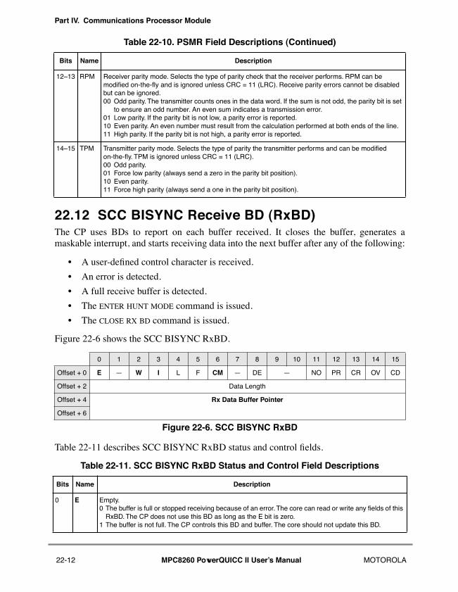
Part IV. Communications Processor Module
22.12 SCC BISYNC Receive BD (RxBD)The CP uses BDs to report on each buffer received. It closes the buffer, generates amaskable interrupt, and starts receiving data into the next buffer after any of the following:
¥ A user-deÞned control character is received.
¥ An error is detected.
¥ A full receive buffer is detected.
¥ The ENTER HUNT MODE command is issued.
¥ The CLOSE RX BD command is issued.
Figure 22-6 shows the SCC BISYNC RxBD.
Table 22-11 describes SCC BISYNC RxBD status and control Þelds.
12Ð13 RPM Receiver parity mode. Selects the type of parity check that the receiver performs. RPM can be modiÞed on-the-ßy and is ignored unless CRC = 11 (LRC). Receive parity errors cannot be disabled but can be ignored.00 Odd parity. The transmitter counts ones in the data word. If the sum is not odd, the parity bit is set
to ensure an odd number. An even sum indicates a transmission error.01 Low parity. If the parity bit is not low, a parity error is reported. 10 Even parity. An even number must result from the calculation performed at both ends of the line.11 High parity. If the parity bit is not high, a parity error is reported.
14Ð15 TPM Transmitter parity mode. Selects the type of parity the transmitter performs and can be modiÞed on-the-ßy. TPM is ignored unless CRC = 11 (LRC).00 Odd parity.01 Force low parity (always send a zero in the parity bit position).10 Even parity.11 Force high parity (always send a one in the parity bit position).
0 1 2 3 4 5 6 7 8 9 10 11 12 13 14 15
Offset + 0 E Ñ W I L F CM Ñ DE Ñ NO PR CR OV CD
Offset + 2 Data Length
Offset + 4 Rx Data Buffer Pointer
Offset + 6
Figure 22-6. SCC BISYNC RxBD
Table 22-11. SCC BISYNC RxBD Status and Control Field Descriptions
Bits Name Description
0 E Empty. 0 The buffer is full or stopped receiving because of an error. The core can read or write any Þelds of this
RxBD. The CP does not use this BD as long as the E bit is zero.1 The buffer is not full. The CP controls this BD and buffer. The core should not update this BD.
Table 22-10. PSMR Field Descriptions (Continued)
Bits Name Description
22-12 MPC8260 PowerQUICC II UserÕs Manual MOTOROLA
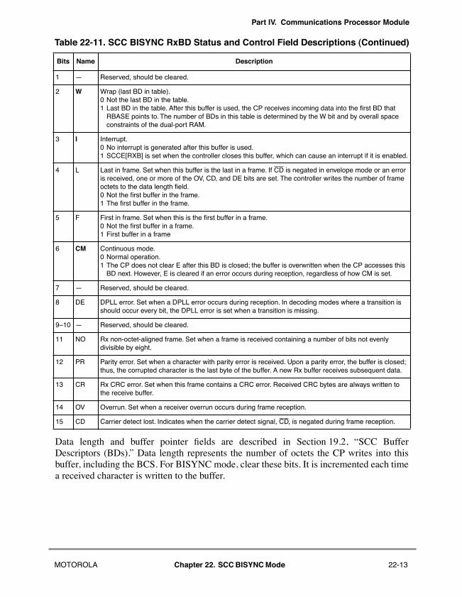
Part IV. Communications Processor Module
Data length and buffer pointer Þelds are described in Section 19.2, ÒSCC BufferDescriptors (BDs).Ó Data length represents the number of octets the CP writes into thisbuffer, including the BCS. For BISYNC mode, clear these bits. It is incremented each timea received character is written to the buffer.
1 Ñ Reserved, should be cleared.
2 W Wrap (last BD in table). 0 Not the last BD in the table. 1 Last BD in the table. After this buffer is used, the CP receives incoming data into the Þrst BD that
RBASE points to. The number of BDs in this table is determined by the W bit and by overall space constraints of the dual-port RAM.
3 I Interrupt. 0 No interrupt is generated after this buffer is used. 1 SCCE[RXB] is set when the controller closes this buffer, which can cause an interrupt if it is enabled.
4 L Last in frame. Set when this buffer is the last in a frame. If CD is negated in envelope mode or an error is received, one or more of the OV, CD, and DE bits are set. The controller writes the number of frame octets to the data length Þeld.0 Not the Þrst buffer in the frame.1 The Þrst buffer in the frame.
5 F First in frame. Set when this is the Þrst buffer in a frame.0 Not the Þrst buffer in a frame. 1 First buffer in a frame
6 CM Continuous mode. 0 Normal operation.1 The CP does not clear E after this BD is closed; the buffer is overwritten when the CP accesses this
BD next. However, E is cleared if an error occurs during reception, regardless of how CM is set.
7 Ñ Reserved, should be cleared.
8 DE DPLL error. Set when a DPLL error occurs during reception. In decoding modes where a transition is should occur every bit, the DPLL error is set when a transition is missing.
9Ð10 Ñ Reserved, should be cleared.
11 NO Rx non-octet-aligned frame. Set when a frame is received containing a number of bits not evenly divisible by eight.
12 PR Parity error. Set when a character with parity error is received. Upon a parity error, the buffer is closed; thus, the corrupted character is the last byte of the buffer. A new Rx buffer receives subsequent data.
13 CR Rx CRC error. Set when this frame contains a CRC error. Received CRC bytes are always written to the receive buffer.
14 OV Overrun. Set when a receiver overrun occurs during frame reception.
15 CD Carrier detect lost. Indicates when the carrier detect signal, CD, is negated during frame reception.
Table 22-11. SCC BISYNC RxBD Status and Control Field Descriptions (Continued)
Bits Name Description
MOTOROLA Chapter 22. SCC BISYNC Mode 22-13
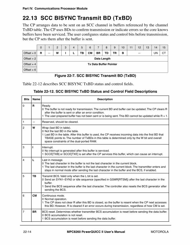
Part IV. Communications Processor Module
22.13 SCC BISYNC Transmit BD (TxBD)The CP arranges data to be sent on an SCC channel in buffers referenced by the channelTxBD table. The CP uses BDs to conÞrm transmission or indicate errors so the core knowsbuffers have been serviced. The user conÞgures status and control bits before transmission,but the CP sets them after the buffer is sent.
Table 22-12 describes SCC BISYNC TxBD status and control Þelds.
0 1 2 3 4 5 6 7 8 9 10 11 12 13 14 15
Offset + 0 R Ñ W I L TB CM BR TD TR B Ñ UN CT
Offset + 2 Data Length
Offset + 4 Tx Data Buffer Pointer
Offset + 6
Figure 22-7. SCC BISYNC Transmit BD (TxBD)
Table 22-12. SCC BISYNC TxBD Status and Control Field Descriptions
Bits Name Description
0 R Ready. 0 The buffer is not ready for transmission. The current BD and buffer can be updated. The CP clears R
after the buffer is sent or after an error condition.1 The user-prepared buffer has not been sent or is being sent. This BD cannot be updated while R = 1.
1 Ñ Reserved, should be cleared.
2 W Wrap (last BD in table). 0 Not the last BD in the table. 1 Last BD in the table. After this buffer is used, the CP receives incoming data into the Þrst BD that
TBASE points to. The number of TxBDs in this table is determined only by the W bit and overall space constraints of the dual-ported RAM.
3 I Interrupt. 0 No interrupt is generated after this buffer is serviced. 1 SCCE[TXB] or SCCE[TXE] is set after the CP services this buffer, which can cause an interrupt.
4 L Last in message. 0 The last character in the buffer is not the last character in the current block. 1 The last character in the buffer is the last character in the current block. The transmitter enters and
stays in normal mode after sending the last character in the buffer and the BCS, if enabled.
5 TB Transmit BCS. Valid only when the L bit is set. 0 Send an SYN1ÐSYN2 or idle sequence (speciÞed in GSMR[RTSM]) after the last character in the
buffer.1 Send the BCS sequence after the last character. The controller also resets the BCS generator after
sending the BCS.
6 CM Continuous mode. 0 Normal operation.1 The CP does not clear R after this BD is closed, so the buffer is resent when the CP next accesses
this BD. However, R is cleared if an error occurs during transmission, regardless of how CM is set.
7 BR BCS reset. Determines whether transmitter BCS accumulation is reset before sending the data buffer.0 BCS accumulation is not reset. 1 BCS accumulation is reset before sending the data buffer.
22-14 MPC8260 PowerQUICC II UserÕs Manual MOTOROLA
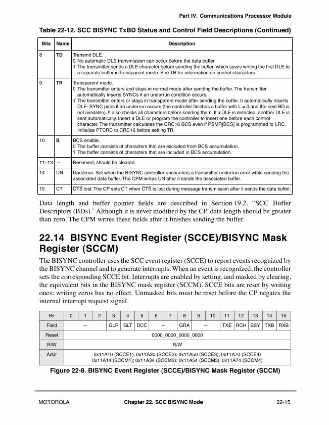
Part IV. Communications Processor Module
Data length and buffer pointer Þelds are described in Section 19.2, ÒSCC BufferDescriptors (BDs).Ó Although it is never modiÞed by the CP, data length should be greaterthan zero. The CPM writes these Þelds after it Þnishes sending the buffer.
22.14 BISYNC Event Register (SCCE)/BISYNC Mask Register (SCCM)The BISYNC controller uses the SCC event register (SCCE) to report events recognized bythe BISYNC channel and to generate interrupts. When an event is recognized, the controllersets the corresponding SCCE bit. Interrupts are enabled by setting, and masked by clearing,the equivalent bits in the BISYNC mask register (SCCM). SCCE bits are reset by writingones; writing zeros has no effect. Unmasked bits must be reset before the CP negates theinternal interrupt request signal.
8 TD Transmit DLE. 0 No automatic DLE transmission can occur before the data buffer. 1 The transmitter sends a DLE character before sending the buffer, which saves writing the Þrst DLE to
a separate buffer in transparent mode. See TR for information on control characters.
9 TR Transparent mode. 0 The transmitter enters and stays in normal mode after sending the buffer. The transmitter
automatically inserts SYNCs if an underrun condition occurs. 1 The transmitter enters or stays in transparent mode after sending the buffer. It automatically inserts
DLEÐSYNC pairs if an underrun occurs (the controller Þnishes a buffer with L = 0 and the next BD is not available). It also checks all characters before sending them. If a DLE is detected, another DLE is sent automatically. Insert a DLE or program the controller to insert one before each control character. The transmitter calculates the CRC16 BCS even if PSMR[BCS] is programmed to LRC. Initialize PTCRC to CRC16 before setting TR.
10 B BCS enable. 0 The buffer consists of characters that are excluded from BCS accumulation. 1 The buffer consists of characters that are included in BCS accumulation.
11Ð13 Ñ Reserved, should be cleared.
14 UN Underrun. Set when the BISYNC controller encounters a transmitter underrun error while sending the associated data buffer. The CPM writes UN after it sends the associated buffer.
15 CT CTS lost. The CP sets CT when CTS is lost during message transmission after it sends the data buffer.
Bit 0 1 2 3 4 5 6 7 8 9 10 11 12 13 14 15
Field Ñ GLR GLT DCC Ñ GRA Ñ TXE RCH BSY TXB RXB
Reset 0000_0000_0000_0000
R/W R/W
Addr 0x11A10 (SCCE1); 0x11A30 (SCCE2); 0x11A50 (SCCE3); 0x11A70 (SCCE4)0x11A14 (SCCM1); 0x11A34 (SCCM2); 0x11A54 (SCCM3); 0x11A74 (SCCM4)
Figure 22-8. BISYNC Event Register (SCCE)/BISYNC Mask Register (SCCM)
Table 22-12. SCC BISYNC TxBD Status and Control Field Descriptions (Continued)
Bits Name Description
MOTOROLA Chapter 22. SCC BISYNC Mode 22-15
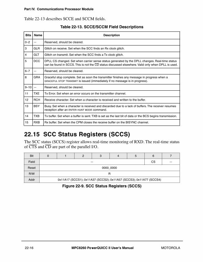
Part IV. Communications Processor Module
Table 22-13 describes SCCE and SCCM Þelds.
22.15 SCC Status Registers (SCCS)The SCC status (SCCS) register allows real-time monitoring of RXD. The real-time statusof CTS and CD are part of the parallel I/O.
Table 22-13. SCCE/SCCM Field Descriptions
Bits Name Description
0Ð2 Ñ Reserved, should be cleared.
3 GLR Glitch on receive. Set when the SCC Þnds an Rx clock glitch.
4 GLT Glitch on transmit. Set when the SCC Þnds a Tx clock glitch.
5 DCC DPLL CS changed. Set when carrier sense status generated by the DPLL changes. Real-time status can be found in SCCS. This is not the CD status discussed elsewhere. Valid only when DPLL is used.
6Ð7 Ñ Reserved, should be cleared.
8 GRA Graceful stop complete. Set as soon the transmitter Þnishes any message in progress when a GRACEFUL STOP TRANSMIT is issued (immediately if no message is in progress).
9Ð10 Ñ Reserved, should be cleared.
11 TXE Tx Error. Set when an error occurs on the transmitter channel.
12 RCH Receive character. Set when a character is received and written to the buffer.
13 BSY Busy. Set when a character is received and discarded due to a lack of buffers. The receiver resumes reception after an ENTER HUNT MODE command.
14 TXB Tx buffer. Set when a buffer is sent. TXB is set as the last bit of data or the BCS begins transmission.
15 RXB Rx buffer. Set when the CPM closes the receive buffer on the BISYNC channel.
Bit 0 1 2 3 4 5 6 7
Field Ñ CS Ñ
Reset 0000_0000
R/W R
Addr 0x11A17 (SCCS1); 0x11A37 (SCCS2); 0x11A57 (SCCS3); 0x11A77 (SCCS4)
Figure 22-9. SCC Status Registers (SCCS)
22-16 MPC8260 PowerQUICC II UserÕs Manual MOTOROLA
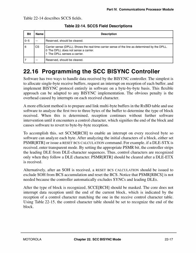
Part IV. Communications Processor Module
Table 22-14 describes SCCS Þelds.
22.16 Programming the SCC BISYNC ControllerSoftware has two ways to handle data received by the BISYNC controller. The simplest isto allocate single-byte receive buffers, request an interrupt on reception of each buffer, andimplement BISYNC protocol entirely in software on a byte-by-byte basis. This ßexibleapproach can be adapted to any BISYNC implementation. The obvious penalty is theoverhead caused by interrupts on each received character.
A more efÞcient method is to prepare and link multi-byte buffers in the RxBD table and usesoftware to analyze the Þrst two to three bytes of the buffer to determine the type of blockreceived. When this is determined, reception continues without further softwareintervention until it encounters a control character, which signiÞes the end of the block andcauses software to revert to byte-by-byte reception.
To accomplish this, set SCCM[RCH] to enable an interrupt on every received byte sosoftware can analyze each byte. After analyzing the initial characters of a block, either setPSMR[RTR] or issue a RESET BCS CALCULATION command. For example, if a DLE-STX isreceived, enter transparent mode. By setting the appropriate PSMR bit, the controller stripsthe leading DLE from DLE-character sequences. Thus, control characters are recognizedonly when they follow a DLE character. PSMR[RTR] should be cleared after a DLE-ETXis received.
Alternatively, after an SOH is received, a RESET BCS CALCULATION should be issued toexclude SOH from BCS accumulation and reset the BCS. Notice that PSMR[RBCS] is notneeded because the controller automatically excludes SYNCs and leading DLEs.
After the type of block is recognized, SCCE[RCH] should be masked. The core does notinterrupt data reception until the end of the current block, which is indicated by thereception of a control character matching the one in the receive control character table.Using Table 22-15, the control character table should be set to recognize the end of theblock.
Table 22-14. SCCS Field Descriptions
Bit Name Description
0Ð5 Ñ Reserved, should be cleared.
6 CS Carrier sense (DPLL). Shows the real-time carrier sense of the line as determined by the DPLL. 0 The DPLL does not sense a carrier.1 The DPLL senses a carrier.
7 Ñ Reserved, should be cleared.
MOTOROLA Chapter 22. SCC BISYNC Mode 22-17
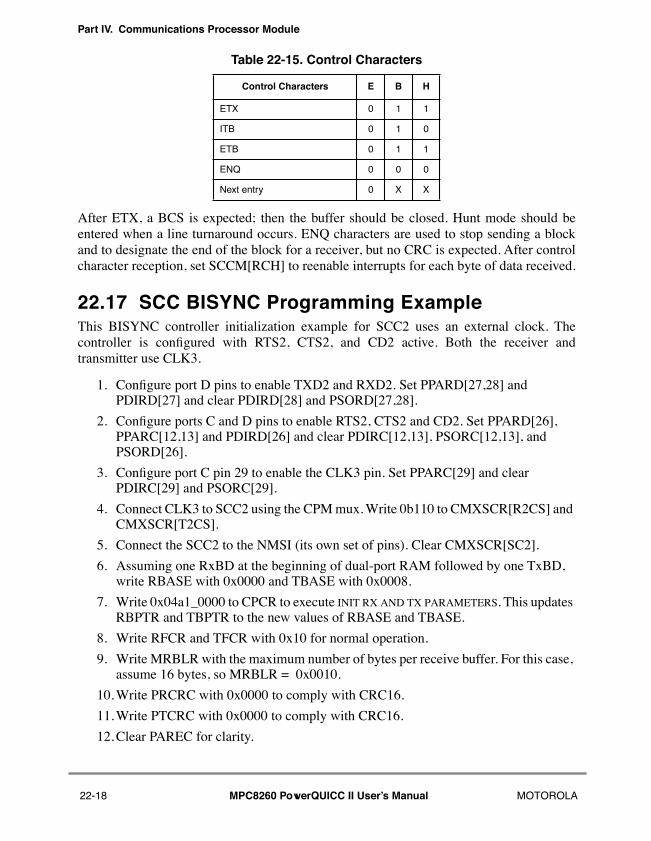
Part IV. Communications Processor Module
After ETX, a BCS is expected; then the buffer should be closed. Hunt mode should beentered when a line turnaround occurs. ENQ characters are used to stop sending a blockand to designate the end of the block for a receiver, but no CRC is expected. After controlcharacter reception, set SCCM[RCH] to reenable interrupts for each byte of data received.
22.17 SCC BISYNC Programming ExampleThis BISYNC controller initialization example for SCC2 uses an external clock. Thecontroller is conÞgured with RTS2, CTS2, and CD2 active. Both the receiver andtransmitter use CLK3.
1. ConÞgure port D pins to enable TXD2 and RXD2. Set PPARD[27,28] and PDIRD[27] and clear PDIRD[28] and PSORD[27,28].
2. ConÞgure ports C and D pins to enable RTS2, CTS2 and CD2. Set PPARD[26], PPARC[12,13] and PDIRD[26] and clear PDIRC[12,13], PSORC[12,13], and PSORD[26].
3. ConÞgure port C pin 29 to enable the CLK3 pin. Set PPARC[29] and clear PDIRC[29] and PSORC[29].
4. Connect CLK3 to SCC2 using the CPM mux. Write 0b110 to CMXSCR[R2CS] and CMXSCR[T2CS].
5. Connect the SCC2 to the NMSI (its own set of pins). Clear CMXSCR[SC2].
6. Assuming one RxBD at the beginning of dual-port RAM followed by one TxBD, write RBASE with 0x0000 and TBASE with 0x0008.
7. Write 0x04a1_0000 to CPCR to execute INIT RX AND TX PARAMETERS. This updates RBPTR and TBPTR to the new values of RBASE and TBASE.
8. Write RFCR and TFCR with 0x10 for normal operation.
9. Write MRBLR with the maximum number of bytes per receive buffer. For this case, assume 16 bytes, so MRBLR = 0x0010.
10. Write PRCRC with 0x0000 to comply with CRC16.
11. Write PTCRC with 0x0000 to comply with CRC16.
12. Clear PAREC for clarity.
Table 22-15. Control Characters
Control Characters E B H
ETX 0 1 1
ITB 0 1 0
ETB 0 1 1
ENQ 0 0 0
Next entry 0 X X
22-18 MPC8260 PowerQUICC II UserÕs Manual MOTOROLA
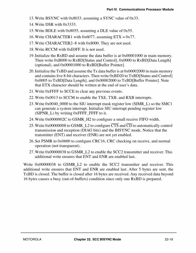
Part IV. Communications Processor Module
13. Write BSYNC with 0x8033, assuming a SYNC value of 0x33.
14. Write DSR with 0x3333.
15. Write BDLE with 0x8055, assuming a DLE value of 0x55.
16. Write CHARACTER1 with 0x6077, assuming ETX = 0x77.
17. Write CHARACTER2Ð8 with 0x8000. They are not used.
18. Write RCCM with 0xE0FF. It is not used.
19. Initialize the RxBD and assume the data buffer is at 0x00001000 in main memory. Then write 0xB000 to RxBD[Status and Control], 0x0000 to RxBD[Data Length] (optional), and 0x00001000 to RxBD[Buffer Pointer].
20. Initialize the TxBD and assume the Tx data buffer is at 0x00002000 in main memory and contains Þve 8-bit characters. Then write 0xBD20 to TxBD[Status and Control] 0x0005 to TxBD[Data Length], and 0x00002000 to TxBD[Buffer Pointer]. Note that ETX character should be written at the end of userÕs data.
21. Write 0xFFFF to SCCE to clear any previous events.
22. Write 0x0013 to SCCM to enable the TXE, TXB, and RXB interrupts.
23. Write 0x0040_0000 to the SIU interrupt mask register low (SIMR_L) so the SMC1 can generate a system interrupt. Initialize SIU interrupt pending register low (SIPNR_L) by writing 0xFFFF_FFFF to it.
24. Write 0x0000002C to GSMR_H2 to conÞgure a small receive FIFO width.
25. Write 0x00000008 to GSMR_L2 to conÞgure CTS and CD to automatically control transmission and reception (DIAG bits) and the BISYNC mode. Notice that the transmitter (ENT) and receiver (ENR) are not yet enabled.
26. Set PSMR to 0x0600 to conÞgure CRC16, CRC checking on receive, and normal operation (not transparent).
27. Write 0x00000038 to GSMR_L2 to enable the SCC2 transmitter and receiver. This additional write ensures that ENT and ENR are enabled last.
Write 0x00000038 to GSMR_L2 to enable the SCC2 transmitter and receiver. Thisadditional write ensures that ENT and ENR are enabled last. After 5 bytes are sent, theTxBD is closed. The buffer is closed after 16 bytes are received. Any received data beyond16 bytes causes a busy (out-of-buffers) condition since only one RxBD is prepared.
MOTOROLA Chapter 22. SCC BISYNC Mode 22-19
Part IV. Communications Processor Module
22-20 MPC8260 PowerQUICC II UserÕs Manual MOTOROLA
Chapter 23 SCC Transparent Mode230230
Transparent mode (also called totally transparent or promiscuous mode) provides a clearchannel on which the SCC can send or receive serial data without bit-level manipulation.Software implements protocols run over transparent mode. An SCC in transparent modefunctions as a high-speed serial-to-parallel and parallel-to-serial converter.
Transparent mode can be used for serially moving data that requires no superimposedprotocol, for applications that require serial-to-parallel and parallel-to-serial conversion forcommunication among chips on the same board, and for applications that require data to beswitched without interfering with the protocol encoding itself, such as when data from ahigh-speed time-multiplexed serial stream is multiplexed into low-speed data streams. Theconcept is to switch the data path without altering the protocol encoded on that data path.
Transparent mode is conÞgured in the GSMR; see Section 19.1.1, ÒThe General SCC ModeRegisters (GSMR1ÐGSMR4).Ó Transparent mode is selected in GSMR_H[TTX, TRX] forthe transmitter and receiver, respectively. Setting both bits enables full-duplex transparentoperation. If only one is set, the other half of the SCC uses the protocol speciÞed inGSMR_L[MODE]. This allows loop-back modes to DMA data from one memory locationto another while data is converted to a speciÞc serial format.
The SCC operations are asynchronous with the core and can be synchronous orasynchronous with other SCCs. Each clock can be supplied from the internal baud rategenerator bank, DPLL output, or external pins.
The SCC can work with the time-slot assigner (TSA) or nonmultiplexed serial interface(NMSI) and supports modem lines with the general-purpose I/O pins. Data can betransferred either the msb or lsb Þrst in each octet.
23.1 FeaturesThe following list summarizes the main features of the SCC in transparent mode:
¥ Flexible buffers¥ Automatic SYNC detection on receive¥ CRCs can be sent and received¥ Reverse data mode
MOTOROLA Chapter 23. SCC Transparent Mode 23-1
Part IV. Communications Processor Module
¥ Another protocol can be performed on the other half of the SCC ¥ MC68360-compatible SYNC options
23.2 SCC Transparent Channel Frame Transmission Process
The transparent transmitter is designed to work almost no intervention from the core. Whenthe core enables the SCC transmitter in transparent mode, it starts sending idles, which arelogic high or encoded ones, as programmed in GSMR_L[TEND]. The SCC polls the ÞrstBD in the TxBD table. When there is a message to send, the SCC fetches data frommemory, loads the transmit FIFO, and waits for transmitter synchronization, which isachieved with CTS or by waiting for the receiver to achieve synchronization, depending onGSMR_H[TXSY]. Transmission begins when transmitter synchronization is achieved.
When all BD data has been sent, if TxBD[L] is set, the SCC writes the message status bitsinto the BD, clears TxBD[R], and sends idles until the next BD is ready. If it is ready, someidles are still sent. The transmitter resumes sending only after it achieves synchronization.
If TxBD[L] is cleared when the end of the BD is reached, only TxBD[R] is cleared and thetransmitter moves immediately to the next buffer to begin transmission with no gap on theserial line between buffers. Failure to provide the next buffer in time causes a transmitunderrun which sets SCCE[TXE].
In both cases, an interrupt is issued according to TxBD[I]. By appropriately settingTxBD[I] in each BD, interrupts are generated after each buffer or group of buffers is sent.The SCC then proceeds to the next BD in the table and any whole number of bytes can besent. If GSMR_H[REVD] is set, the bit order of each byte is reversed before being sent; themsb of each octet is sent Þrst.
Setting GSMR_H[TFL] makes the transmit FIFO smaller and reduces transmitter latency,but it can cause transmitter underruns at higher transmission speeds. An optional CRC,selected in GSMR_H[TCRC], can be appended to each transparent frame if it is enabled inthe TxBD.
When the time-slot assigner (TSA) is used with a transparent-mode channel,synchronization is provided by the TSA. There is a start-up delay for the transmitter, butdelays will always be some whole number of complete TSA frames. This means that n-bytetransmit buffers can be mapped directly into n-byte time slots in the TSA frames.
23.3 SCC Transparent Channel Frame Reception Process
When the core enables the SCC receiver in transparent mode, it waits to achievesynchronization before data is received. The receiver can be synchronized to the data by asynchronization pulse or SYNC pattern.
23-2 MPC8260 PowerQUICC II UserÕs Manual MOTOROLA
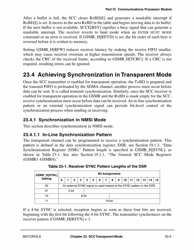
Part IV. Communications Processor Module
After a buffer is full, the SCC clears RxBD[E] and generates a maskable interrupt ifRxBD[I] is set. It moves to the next RxBD in the table and begins moving data to its buffer.If the next buffer is not available, SCCE[BSY] signiÞes a busy signal that can generate amaskable interrupt. The receiver reverts to hunt mode when an ENTER HUNT MODE
command or an error is received. If GSMR_H[REVD] is set, the bit order of each byte isreversed before it is written to memory.
Setting GSMR_H[RFW] reduces receiver latency by making the receive FIFO smaller,which may cause receiver overruns at higher transmission speeds. The receiver alwayschecks the CRC of the received frame, according to GSMR_H[TCRC]. If a CRC is notrequired, resulting errors can be ignored.
23.4 Achieving Synchronization in Transparent ModeOnce the SCC transmitter is enabled for transparent operation, the TxBD is prepared andthe transmit FIFO is preloaded by the SDMA channel, another process must occur beforedata can be sent. It is called transmit synchronization. Similarly, once the SCC receiver isenabled for transparent operation in the GSMR and the RxBD is made empty for the SCC,receive synchronization must occur before data can be received. An in-line synchronizationpattern or an external synchronization signal can provide bit-level control of thesynchronization process when sending or receiving.
23.4.1 Synchronization in NMSI ModeThis section describes synchronization in NMSI mode.
23.4.1.1 In-Line Synchronization PatternThe transparent channel can be programmed to receive a synchronization pattern. Thispattern is deÞned in the data synchronization register, DSR; see Section 19.1.3, ÒDataSynchronization Register (DSR).Ó Pattern length is speciÞed in GSMR_H[SYNL], asshown in Table 23-1. See also Section 19.1.1, ÒThe General SCC Mode Registers(GSMR1ÐGSMR4).Ó
If a 4-bit SYNC is selected, reception begins as soon as these four bits are received,beginning with the Þrst bit following the 4-bit SYNC. The transmitter synchronizes on thereceiver pattern if GSMR_H[RSYN] = 1.
Table 23-1. Receiver SYNC Pattern Lengths of the DSR
GSMR_H[SYNL] Setting
Bit Assignments
0 1 2 3 4 5 6 7 8 9 10 11 12 13 14 15
00 An external SYNC signal is used instead of the SYNC pattern in the DSR.
01 4-bit
10 8-bit
11 16-bit
MOTOROLA Chapter 23. SCC Transparent Mode 23-3
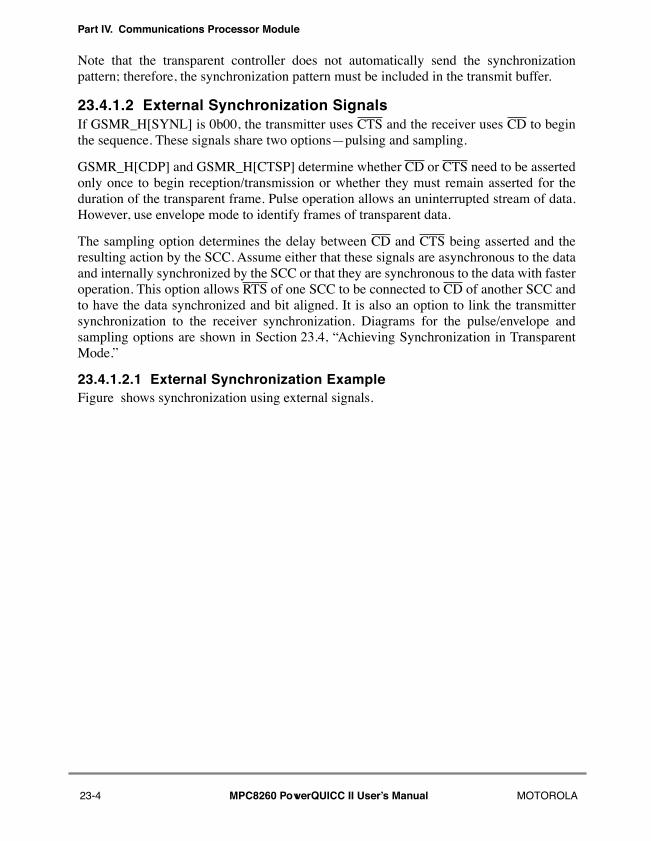
Part IV. Communications Processor Module
Note that the transparent controller does not automatically send the synchronizationpattern; therefore, the synchronization pattern must be included in the transmit buffer.
23.4.1.2 External Synchronization SignalsIf GSMR_H[SYNL] is 0b00, the transmitter uses CTS and the receiver uses CD to beginthe sequence. These signals share two optionsÑpulsing and sampling.
GSMR_H[CDP] and GSMR_H[CTSP] determine whether CD or CTS need to be assertedonly once to begin reception/transmission or whether they must remain asserted for theduration of the transparent frame. Pulse operation allows an uninterrupted stream of data.However, use envelope mode to identify frames of transparent data.
The sampling option determines the delay between CD and CTS being asserted and theresulting action by the SCC. Assume either that these signals are asynchronous to the dataand internally synchronized by the SCC or that they are synchronous to the data with fasteroperation. This option allows RTS of one SCC to be connected to CD of another SCC andto have the data synchronized and bit aligned. It is also an option to link the transmittersynchronization to the receiver synchronization. Diagrams for the pulse/envelope andsampling options are shown in Section 23.4, ÒAchieving Synchronization in TransparentMode.Ó
23.4.1.2.1 External Synchronization ExampleFigure shows synchronization using external signals.
23-4 MPC8260 PowerQUICC II UserÕs Manual MOTOROLA
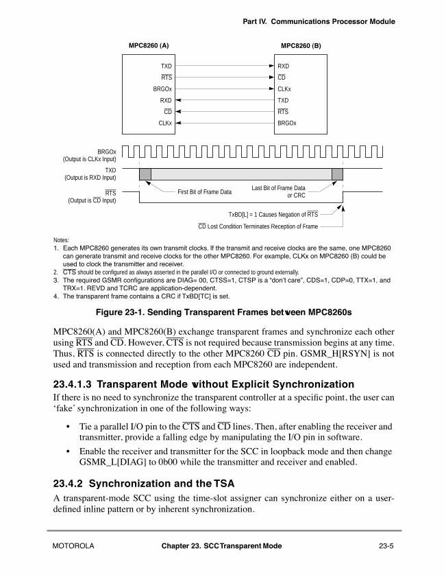
Part IV. Communications Processor Module
Figure 23-1. Sending Transparent Frames between MPC8260s
MPC8260(A) and MPC8260(B) exchange transparent frames and synchronize each otherusing RTS and CD. However, CTS is not required because transmission begins at any time.Thus, RTS is connected directly to the other MPC8260 CD pin. GSMR_H[RSYN] is notused and transmission and reception from each MPC8260 are independent.
23.4.1.3 Transparent Mode without Explicit SynchronizationIf there is no need to synchronize the transparent controller at a speciÞc point, the user canÔfakeÕ synchronization in one of the following ways:
¥ Tie a parallel I/O pin to the CTS and CD lines. Then, after enabling the receiver and transmitter, provide a falling edge by manipulating the I/O pin in software.
¥ Enable the receiver and transmitter for the SCC in loopback mode and then change GSMR_L[DIAG] to 0b00 while the transmitter and receiver and enabled.
23.4.2 Synchronization and the TSAA transparent-mode SCC using the time-slot assigner can synchronize either on a user-deÞned inline pattern or by inherent synchronization.
RXD
CD
CLKx
TXD
RTSCD
RXD
BRGOx
RTS
TXD
CLKx BRGOx
BRGOx
Last Bit of Frame DataFirst Bit of Frame Data
(Output is CLKx Input)
TXD(Output is RXD Input)
RTS(Output is CD Input)
or CRC
TxBD[L] = 1 Causes Negation of RTS
CD Lost Condition Terminates Reception of Frame
MPC8260 (A) MPC8260 (B)
Notes:1. Each MPC8260 generates its own transmit clocks. If the transmit and receive clocks are the same, one MPC8260
can generate transmit and receive clocks for the other MPC8260. For example, CLKx on MPC8260 (B) could be used to clock the transmitter and receiver.
2. CTS should be configured as always asserted in the parallel I/O or connected to ground externally.3. The required GSMR conÞgurations are DIAG= 00, CTSS=1, CTSP is a ÒdonÕt careÓ, CDS=1, CDP=0, TTX=1, and
TRX=1. REVD and TCRC are application-dependent.4. The transparent frame contains a CRC if TxBD[TC] is set.
MOTOROLA Chapter 23. SCC Transparent Mode 23-5
Part IV. Communications Processor Module
Note that when using the TSA, a newly-enabled transmitter sends from 10 to 15 frames ofidles before sending the actual transparent data due to startup requirements of the TDM.Therefore, when loopback testing through the TDM, expect to receive several bytes of 0xFFbefore the actual data.
23.4.2.1 Inline Synchronization PatternThe receiver can be programmed to begin receiving data into the receive buffers only aftera speciÞed data pattern arrives. To synchronize on an inline pattern:
¥ Set GSMR_H[SYNL].
¥ Program the DSR with the desired pattern.
¥ Clear GSMR_H[CDP].
¥ Set GSMR_H[CTSP, CTSS, CDS].
If GSMR_H[TXSY] is also used, the transmitter begins transmission eight clocks after thereceiver achieves synchronization.
23.4.2.2 Inherent SynchronizationInherent synchronization assumes synchronization by default when the channel is enabled;all data sent from the TDM to the SCC is received. To implement inherent synchronization:
¥ Set GSMR_H[CDP, CDS, CTSP, CTSS].
If these bits are not set, the received bit stream will be bit-shifted. The SCC loses the Þrstreceived bit because CD and CTS are treated as asynchronous signals.
23.4.3 End of Frame DetectionAn end of frame cannot be detected in the transparent data stream since there is no deÞnedclosing ßag in transparent mode. Therefore, if framing is needed, the user must use the CDline to alert the transparent controller of an end of frame.
23.5 CRC Calculation in Transparent ModeThe CRC calculations follow the ITU/IEEE standard. The CRC is calculated on thetransmitted data stream; that is, from lsb to msb for non-bit-reversed (GSMR_H[REVD] =0) and from msb to lsb for bit-reversed (GSMR_H[REVD] = 1) transmission. Theappended CRC is sent msb to lsb. When receiving, the CRC is calculated as the incomingbits arrive. The optional reversal of data (GSMR_H[REVD] = 1) is done just before data isstored in memory (after the CRC calculation).
23.6 SCC Transparent Parameter RAMFor transparent mode, the protocol-speciÞc area of the SCC parameter RAM is mapped asin Table 23-2.
23-6 MPC8260 PowerQUICC II UserÕs Manual MOTOROLA

Part IV. Communications Processor Module
CRC_P and CRC_C overlap with the CRC parameters for the HDLC-based protocols.However, this overlap is not detrimental since the CRC constant is used only for the receiverand the CRC preset is used only for the transmitter, so only one entry is required for each.Thus, the user can choose an HDLC transmitter with a transparent receiver or a transparenttransmitter with an HDLC receiver.
23.7 SCC Transparent CommandsThe following transmit and receive commands are issued to the CP command register.Table 23-3 describes transmit commands.
Table 23-2. SCC Transparent Parameter RAM Memory Map
Offset1
1From SCC base address. See Section 19.3.1, ÒSCC Base Addresses.Ó
Name Width Description
0x 30 CRC_P Long CRC preset for totally transparent. For the 16-bit CRC-CCITT, initialize with 0x0000_FFFF. For the 32-bit CRC-CCITT, initialize with 0xFFFF_FFFF and for the CRC-16, initialize with ones (0x0000_FFFF) or zeros (0x0000_0000).
0x 34 CRC_C Long CRC constant for totally transparent receiver. For the 16-bit CRC-CCITT, initialize with 0x0000_F0B8. For the 32-bit CRC-CCITT, CRC_C initialize with 0xDEBB_20E3 and for the CRC-16, which is normally used with BISYNC, initialize with 0x0000_0000.
Table 23-3. Transmit Commands
Command Description
STOP TRANSMIT
After hardware or software is reset and the channel is enabled in the GSMR, the channel is in transmit enable mode and starts polling the Þrst BD every 64 clocks (or immediately if TODR[TOD] = 1). STOP TRANSMIT disables frame transmission on the transmit channel. If the transparent controller receives the command during frame transmission, transmission is aborted after a maximum of 64 additional bits and the transmit FIFO is ßushed. The current TxBD pointer (TBPTR) is not advanced, no new BD is accessed and no new buffers are sent for this channel. The transmitter will send idles.
GRACEFUL STOP TRANSMIT
Stops transmission smoothly, rather than abruptly, in much the same way that the regular STOP TRANSMIT command stops. It stops transmission after the current frame Þnishes or immediately if no frame is being sent. A transparent frame is not complete until a BD with TxBD[L] set has its buffer completely sent. SCCE[GRA] is set once transmission stops; transmit parameters and their BDs can then be modiÞed. The current TxBD pointer (TBPTR) advances to the next TxBD in the table. Transmission resumes once TxBD[R] is set and a RESTART TRANSMIT command is issued.
RESTART TRANSMIT
Reenables transmission of characters on the transmit channel. The transparent controller expects it after a STOP TRANSMIT command is issued (at which point the channel is disabled in SCCM), after a GRACEFUL STOP TRANSMIT command is issued, or after a transmitter error. The transparent controller resumes transmission from the current TBPTR in the channel TxBD table.
INIT TX PARAMETERS
Initializes all transmit parameters in the serial channel parameter RAM to reset state. Issue only when the transmitter is disabled. INIT TX AND RX PARAMETERS resets receive and transmit parameters.
MOTOROLA Chapter 23. SCC Transparent Mode 23-7
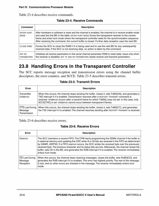
Part IV. Communications Processor Module
Table 23-4 describes receive commands.
23.8 Handling Errors in the Transparent ControllerThe SCC reports message reception and transmission errors using the channel bufferdescriptors, the error counters, and SCCE. Table 23-5 describes transmit errors.
Table 23-6 describes receive errors.
Table 23-4. Receive Commands
Command Description
ENTER HUNT MODE
After hardware or software is reset and the channel is enabled, the channel is in receive enable mode and uses the Þrst BD in the table. ENTER HUNT MODE forces the transparent receiver to the current frame and enter hunt mode where the transparent controller waits for the synchronization sequence. After receiving the command, the current buffer is closed. Further data reception uses the next BD.
CLOSE RXBD Forces the SCC to close the RxBD if it is being used and to use the next BD for any subsequently received data. If the SCC is not receiving data, no action is taken by this command.
INIT RX PARAMETERS
Initializes all receive parameters in this serial channel parameter RAM to reset state. Issue only when the receiver is disabled. INIT TX AND RX PARAMETERS resets receive and transmit parameters.
Table 23-5. Transmit Errors
Error Description
Transmitter Underrun
When this occurs, the channel stops sending the buffer, closes it, sets TxBD[UN], and generates a TXE interrupt if it is enabled. Transmission resumes after a RESTART TRANSMIT command is received. Underrun occurs after a transmit frame for which TxBD[L] was not set. In this case, only SCCE[TXE] is set. Underrun cannot occur between transparent frames.
CTS Lost During Message Transmission
When this occurs, the channel stops sending the buffer, closes it, sets TxBD[CT], and generates the TXE interrupt if it is enabled. The channel resumes sending after RESTART TRANSMIT is received.
Table 23-6. Receive Errors
Error Description
Overrun The SCC maintains a receive FIFO. The CPM starts programming the SDMA channel if the buffer is in external memory and updating the CRC when 8 or 32 bits are received in the FIFO as determined by GSMR_H[RFW]. If a FIFO overrun occurs, the SCC writes the received byte over the previously received byte. The previous character and its status bits are lost. Afterwards, the channel closes the buffer, sets OV in the BD, and generates the RXB interrupt if it is enabled. The receiver immediately enters hunt mode.
CD Lost During Message Reception
When this occurs, the channel stops receiving messages, closes the buffer, sets RxBD[CD], and generates the RXB interrupt if it is enabled. This error has highest priority. The rest of the message is lost, and no other errors are checked in the message. The receiver immediately enters hunt mode.
23-8 MPC8260 PowerQUICC II UserÕs Manual MOTOROLA
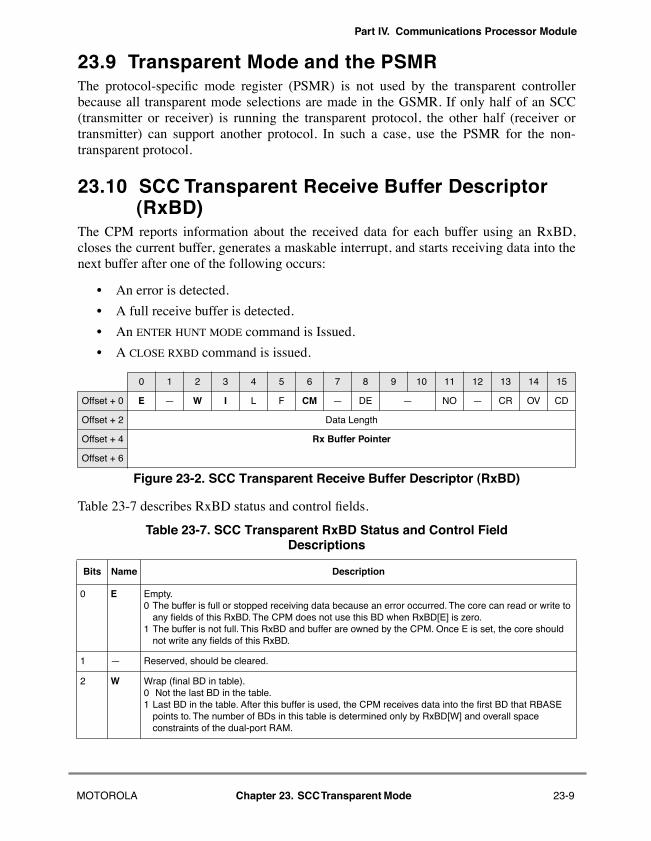
Part IV. Communications Processor Module
23.9 Transparent Mode and the PSMRThe protocol-speciÞc mode register (PSMR) is not used by the transparent controllerbecause all transparent mode selections are made in the GSMR. If only half of an SCC(transmitter or receiver) is running the transparent protocol, the other half (receiver ortransmitter) can support another protocol. In such a case, use the PSMR for the non-transparent protocol.
23.10 SCC Transparent Receive Buffer Descriptor (RxBD)
The CPM reports information about the received data for each buffer using an RxBD,closes the current buffer, generates a maskable interrupt, and starts receiving data into thenext buffer after one of the following occurs:
¥ An error is detected.
¥ A full receive buffer is detected.
¥ An ENTER HUNT MODE command is Issued.
¥ A CLOSE RXBD command is issued.
Table 23-7 describes RxBD status and control Þelds.
0 1 2 3 4 5 6 7 8 9 10 11 12 13 14 15
Offset + 0 E Ñ W I L F CM Ñ DE Ñ NO Ñ CR OV CD
Offset + 2 Data Length
Offset + 4 Rx Buffer Pointer
Offset + 6
Figure 23-2. SCC Transparent Receive Buffer Descriptor (RxBD)
Table 23-7. SCC Transparent RxBD Status and Control Field Descriptions
Bits Name Description
0 E Empty.0 The buffer is full or stopped receiving data because an error occurred. The core can read or write to
any Þelds of this RxBD. The CPM does not use this BD when RxBD[E] is zero.1 The buffer is not full. This RxBD and buffer are owned by the CPM. Once E is set, the core should
not write any Þelds of this RxBD.
1 Ñ Reserved, should be cleared.
2 W Wrap (Þnal BD in table).0 Not the last BD in the table. 1 Last BD in the table. After this buffer is used, the CPM receives data into the Þrst BD that RBASE
points to. The number of BDs in this table is determined only by RxBD[W] and overall space constraints of the dual-port RAM.
MOTOROLA Chapter 23. SCC Transparent Mode 23-9
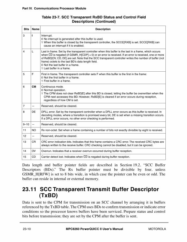
Part IV. Communications Processor Module
Data length and buffer pointer Þelds are described in Section 19.2, ÒSCC BufferDescriptors (BDs).Ó The Rx buffer pointer must be divisible by four, unlessGSMR_H[RFW] is set to 8 bits wide, in which case the pointer can be even or odd. Thebuffer can reside in internal or external memory.
23.11 SCC Transparent Transmit Buffer Descriptor (TxBD)
Data is sent to the CPM for transmission on an SCC channel by arranging it in buffersreferenced by the TxBD table. The CPM uses BDs to conÞrm transmission or indicate errorconditions so the processor knows buffers have been serviced. Prepare status and controlbits before transmission; they are set by the CPM after the buffer is sent.
3 I Interrupt. 0 No interrupt is generated after this buffer is used. 1 When this buffer is closed by the transparent controller, the SCCE[RXB] is set. SCCE[RXB] can
cause an interrupt if it is enabled.
4 L Last in frame. Set by the transparent controller when this buffer is the last in a frame, which occurs when CD is negated (if GSMR_H[CDP] = 0) or an error is received. If an error is received, one or more of RxBD[OV, CD, DE] are set. Note that the SCC transparent controller writes the number of buffer (not frame) octets to the last BDÕs data length Þeld. 0 Not the last buffer in a frame. 1 Last buffer in a frame.
5 F First in frame. The transparent controller sets F when this buffer is the Þrst in the frame:0 Not the Þrst buffer in a frame.1 First buffer in a frame.
6 CM Continuous mode. 0 Normal operation.1 The CPM does not clear RxBD[E] after this BD is closed, letting the buffer be overwritten when the
CPM next accesses this BD. However, RxBD[E] is cleared if an error occurs during reception, regardless of how CM is set.
7 Ñ Reserved, should be cleared.
8 DE DPLL error. Set by the transparent controller when a DPLL error occurs as this buffer is received. In decoding modes, where a transition is promised every bit, DE is set when a missing transition occurs. If a DPLL error occurs, no other error checking is performed.
9Ð10 Ñ Reserved, should be cleared.
11 NO Rx non-octet. Set when a frame containing a number of bits not exactly divisible by eight is received.
12 Ñ Reserved, should be cleared.
13 CR CRC error indication bits. Indicates that this frame contains a CRC error. The received CRC bytes are always written to the receive buffer. CRC checking cannot be disabled, but it can be ignored.
14 OV Overrun. Indicates that a receiver overrun occurred during buffer reception.
15 CD Carrier detect lost. Indicates when CD is negated during buffer reception.
Table 23-7. SCC Transparent RxBD Status and Control Field Descriptions (Continued)
Bits Name Description
23-10 MPC8260 PowerQUICC II UserÕs Manual MOTOROLA
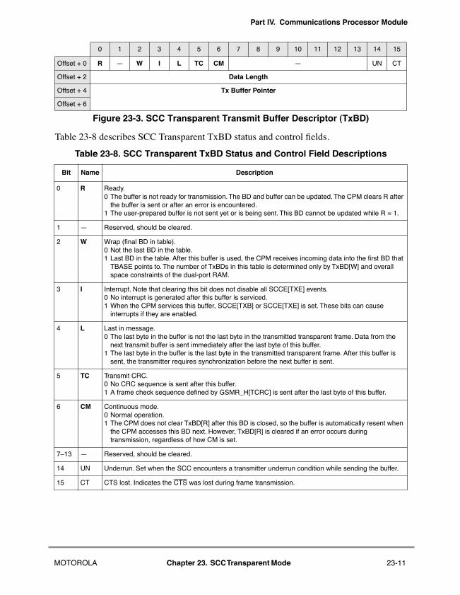
Part IV. Communications Processor Module
Table 23-8 describes SCC Transparent TxBD status and control Þelds.
0 1 2 3 4 5 6 7 8 9 10 11 12 13 14 15
Offset + 0 R Ñ W I L TC CM Ñ UN CT
Offset + 2 Data Length
Offset + 4 Tx Buffer Pointer
Offset + 6
Figure 23-3. SCC Transparent Transmit Buffer Descriptor (TxBD)
Table 23-8. SCC Transparent TxBD Status and Control Field Descriptions
Bit Name Description
0 R Ready. 0 The buffer is not ready for transmission. The BD and buffer can be updated. The CPM clears R after
the buffer is sent or after an error is encountered.1 The user-prepared buffer is not sent yet or is being sent. This BD cannot be updated while R = 1.
1 Ñ Reserved, should be cleared.
2 W Wrap (Þnal BD in table). 0 Not the last BD in the table. 1 Last BD in the table. After this buffer is used, the CPM receives incoming data into the Þrst BD that
TBASE points to. The number of TxBDs in this table is determined only by TxBD[W] and overall space constraints of the dual-port RAM.
3 I Interrupt. Note that clearing this bit does not disable all SCCE[TXE] events.0 No interrupt is generated after this buffer is serviced. 1 When the CPM services this buffer, SCCE[TXB] or SCCE[TXE] is set. These bits can cause
interrupts if they are enabled.
4 L Last in message. 0 The last byte in the buffer is not the last byte in the transmitted transparent frame. Data from the
next transmit buffer is sent immediately after the last byte of this buffer. 1 The last byte in the buffer is the last byte in the transmitted transparent frame. After this buffer is
sent, the transmitter requires synchronization before the next buffer is sent.
5 TC Transmit CRC. 0 No CRC sequence is sent after this buffer. 1 A frame check sequence deÞned by GSMR_H[TCRC] is sent after the last byte of this buffer.
6 CM Continuous mode. 0 Normal operation.1 The CPM does not clear TxBD[R] after this BD is closed, so the buffer is automatically resent when
the CPM accesses this BD next. However, TxBD[R] is cleared if an error occurs during transmission, regardless of how CM is set.
7Ð13 Ñ Reserved, should be cleared.
14 UN Underrun. Set when the SCC encounters a transmitter underrun condition while sending the buffer.
15 CT CTS lost. Indicates the CTS was lost during frame transmission.
MOTOROLA Chapter 23. SCC Transparent Mode 23-11
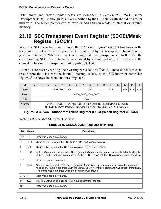
Part IV. Communications Processor Module
Data length and buffer pointer Þelds are described in Section 19.2, ÒSCC BufferDescriptors (BDs).Ó Although it is never modiÞed by the CP, data length should be greaterthan zero. The buffer pointer can be even or odd and can reside in internal or externalmemory.
23.12 SCC Transparent Event Register (SCCE)/Mask Register (SCCM)
When the SCC is in transparent mode, the SCC event register (SCCE) functions as thetransparent event register to report events recognized by the transparent channel and togenerate interrupts. When an event is recognized, the transparent controller sets thecorresponding SCCE bit. Interrupts are enabled by setting, and masked by clearing, theequivalent bits in the transparent mask register (SCCM).
Event bits are reset by writing ones; writing zeros has no effect. All unmasked bits must bereset before the CP clears the internal interrupt request to the SIU interrupt controller.Figure 23-4 shows the event and mask registers.
Table 23-9 describes SCCE/SCCM Þelds.
Bit 0 1 2 3 4 5 6 7 8 9 10 11 12 13 14 15
Field Ñ GLR GLT DCC Ñ GRA Ñ TXE Ñ BSY TXB RXB
Reset 0000_0000_0000_0000
R/W R/W
Address 0x11A10 (SCCE1); 0x11A30 (SCCE2); 0x11A50 (SCCE3); 0x11A70 (SCCE4)0x11A14 (SCCM1); 0x11A34 (SCCM2); 0x11A54 (SCCM3); 0x11A74 (SCCM4)
Figure 23-4. SCC Transparent Event Register (SCCE)/Mask Register (SCCM)
Table 23-9. SCCE/SCCM Field Descriptions
Bit Name Description
0Ð2 Ñ Reserved, should be cleared.
3 GLR Glitch on Rx. Set when the SCC Þnds a glitch on the receive clock.
4 GLT Glitch on Tx. Set when the SCC Þnds a glitch on the transmit clock.
5 DCC DPLL CS changed. Set when the DPLL-generated carrier sense status changes (valid only when the DPLL is used). Real-time status can be read in SCCS. This is not the CD status mentioned elsewhere.
6Ð7 Ñ Reserved, should be cleared.
8 GRA Graceful stop complete. Set when a graceful stop initiated by completes as soon as the transmitter Þnishes any frame in progress when the GRACEFUL STOP TRANSMIT command was issued. Immediately if no frame was in progress when the command was issued.
9Ð10 Ñ Reserved, should be cleared.
11 TXE Tx error. Set when an error occurs on the transmitter channel.
12 Ñ Reserved, should be cleared.
23-12 MPC8260 PowerQUICC II UserÕs Manual MOTOROLA
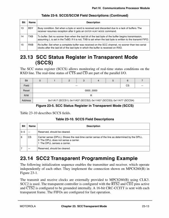
Part IV. Communications Processor Module
23.13 SCC Status Register in Transparent Mode (SCCS)
The SCC status register (SCCS) allows monitoring of real-time status conditions on theRXD line. The real-time status of CTS and CD are part of the parallel I/O.
Table 23-10 describes SCCS Þelds.
23.14 SCC2 Transparent Programming ExampleThe following initialization sequence enables the transmitter and receiver, which operateindependently of each other. They implement the connection shown on MPC8260(B) inFigure 23-1.
The transmit and receive clocks are externally provided to MPC8260(B) using CLK3.SCC2 is used. The transparent controller is conÞgured with the RTS2 and CD2 pins activeand CTS2 is conÞgured to be grounded internally. A 16-bit CRC-CCITT is sent with eachtransparent frame. The FIFOs are conÞgured for fast operation.
13 BSY Busy condition. Set when a byte or word is received and discarded due to a lack of buffers. The receiver resumes reception after it gets an ENTER HUNT MODE command.
14 TXB Tx buffer. Set no sooner than when the last bit of the last byte of the buffer begins transmission, assuming L is set in the TxBD. If it is not, TXB is set when the last byte is written to the transmit FIFO.
15 RXB Rx buffer. Set when a complete buffer was received on the SCC channel, no sooner than two serial clocks after the last bit of the last byte in which the buffer is received on RXD.
Bit 0 1 2 3 4 5 6 7
Field Ñ CS Ñ
Reset 0000_0000
R/W R
Address 0x11A17 (SCCS1); 0x11A37 (SCCS2); 0x11A57 (SCCS3); 0x11A77 (SCCS4)
Figure 23-5. SCC Status Register in Transparent Mode (SCCS)
Table 23-10. SCCS Field Descriptions
Bit Name Description
0Ð5 Ñ Reserved, should be cleared.
6 CS Carrier sense (DPLL). Shows the real-time carrier sense of the line as determined by the DPLL. 0 The DPLL does not sense a carrier.1 The DPLL senses a carrier.
7 Ñ Reserved, should be cleared.
Table 23-9. SCCE/SCCM Field Descriptions (Continued)
Bit Name Description
MOTOROLA Chapter 23. SCC Transparent Mode 23-13
Part IV. Communications Processor Module
1. ConÞgure port D pins to enable TXD2 and RXD2. Set PPARD[27,28] and PDIRD[27] and clear PDIRD[28] and PSORD[27,28].
2. ConÞgure ports C and D pins to enable RTS2, CTS2 and CD2. Set PPARD[26], PPARC[12,13] and PDIRD[26] and clear PDIRC[12,13], PSORC[12,13] and PSORD[26].
3. ConÞgure port C pin 29 to enable the CLK3 pin. Set PPARC[29] and clear PDIRC[29] and PSORC[29].
4. Connect CLK3 to SCC2 using the CPM mux. Program CMXSCR[R2CS] and CMXSCR[T2CS] to 0b110.
5. Connect the SCC2 to the NMSI and clear CMXSCR[SC2].
6. Write RBASE with 0x0000 and TBASE with 0x0008 in the SCC2 parameter RAM to point to one RxBD at the beginning of dual-port RAM followed by one TxBD.
7. Write 0x04A1_0000 to the CPCR to execute INIT RX AND TX PARAMETERS for SCC2.
8. Write 0x0041 to the CPCR to execute INIT RX AND TX PARAMETERS for SCC2.
9. Write RFCR and TFCR with 0x10 for normal operation.
10. Write MRBLR with the maximum number of bytes per receive buffer and assume 16-bytes, so MRBLR = 0x0010.
11. Write CRC_P with 0x0000_FFFF to comply with the 16-bit CRC-CCITT.
12. Write CRC_C with 0x0000_F0B8 to comply with the 16-bit CRC-CCITT.
13. Initialize the RxBD. Assume the Rx buffer is at 0x0000_1000 in main memory. Write 0xB000 to RxBD[Status and Control], 0x0000 to RxBD[Data Length] (optional), and 0x0000_1000 to RxBD[Buffer Pointer].
14. Initialize the TxBD. Assume the Tx buffer is at 0x0000_2000 in main memory and contains Þve 8-bit characters. Write 0xBC00 to TxBD[Status and Control], 0x0005 to TxBD[Data Length], and 0x0000_2000 to TxBD[Buffer Pointer].
15. Write 0xFFFF to SCCE to clear any previous events.
16. Write 0x0013 to SCCM to enable the TXE, TXB, and RXB interrupts.
17. Write 0x0040_0000 to the SIU interrupt mask register low (SIMR_L) so SMC1 can generate a system interrupt. Initialize SIU interrupt pending register low (SIPNR_L) by writing 0xFFFF_FFFF to it.
18. Write 0x0000_1980 to GSMR_H2 to conÞgure the transparent channel.
19. Write 0x0000_0000 to GSMR_L2 to conÞgure CTS and CD to automatically control transmission and reception (DIAG bits). Normal operation of the transmit clock is used. Note that the transmitter (ENT) and receiver (ENR) are not enabled yet.
20. Write 0x0000_0030 to GSMR_L2 to enable the SCC2 transmitter and receiver. This additional write ensures that the ENT and ENR bits are enabled last.
23-14 MPC8260 PowerQUICC II UserÕs Manual MOTOROLA
Part IV. Communications Processor Module
Note that after 5 bytes are sent, the Tx buffer is closed and after 16 bytes are received theRx buffer is closed. Any data received after 16 bytes causes a busy (out-of-buffers)condition since only one RxBD is prepared.
MOTOROLA Chapter 23. SCC Transparent Mode 23-15

Part IV. Communications Processor Module
23-16 MPC8260 PowerQUICC II UserÕs Manual MOTOROLA
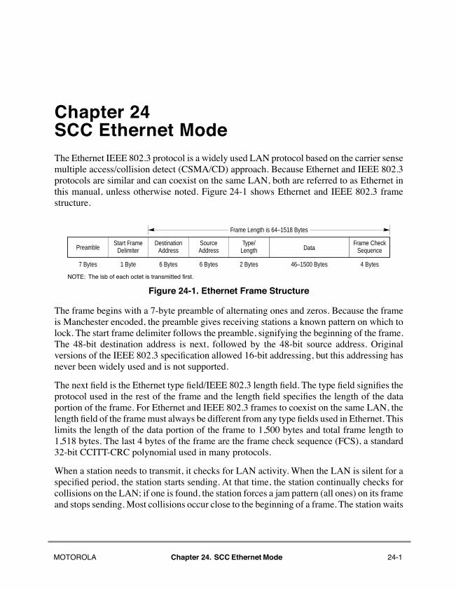
Chapter 24 SCC Ethernet Mode240240
The Ethernet IEEE 802.3 protocol is a widely used LAN protocol based on the carrier sensemultiple access/collision detect (CSMA/CD) approach. Because Ethernet and IEEE 802.3protocols are similar and can coexist on the same LAN, both are referred to as Ethernet inthis manual, unless otherwise noted. Figure 24-1 shows Ethernet and IEEE 802.3 framestructure.
Figure 24-1. Ethernet Frame Structure
The frame begins with a 7-byte preamble of alternating ones and zeros. Because the frameis Manchester encoded, the preamble gives receiving stations a known pattern on which tolock. The start frame delimiter follows the preamble, signifying the beginning of the frame.The 48-bit destination address is next, followed by the 48-bit source address. Originalversions of the IEEE 802.3 speciÞcation allowed 16-bit addressing, but this addressing hasnever been widely used and is not supported.
The next Þeld is the Ethernet type Þeld/IEEE 802.3 length Þeld. The type Þeld signiÞes theprotocol used in the rest of the frame and the length Þeld speciÞes the length of the dataportion of the frame. For Ethernet and IEEE 802.3 frames to coexist on the same LAN, thelength Þeld of the frame must always be different from any type Þelds used in Ethernet. Thislimits the length of the data portion of the frame to 1,500 bytes and total frame length to1,518 bytes. The last 4 bytes of the frame are the frame check sequence (FCS), a standard32-bit CCITT-CRC polynomial used in many protocols.
When a station needs to transmit, it checks for LAN activity. When the LAN is silent for aspeciÞed period, the station starts sending. At that time, the station continually checks forcollisions on the LAN; if one is found, the station forces a jam pattern (all ones) on its frameand stops sending. Most collisions occur close to the beginning of a frame. The station waits
PreambleStart Frame
DataDelimiterDestination
AddressType/
LengthSourceAddress
Frame CheckSequence
7 Bytes 1 Byte 6 Bytes 6 Bytes 2 Bytes 46–1500 Bytes 4 Bytes
Frame Length is 64–1518 Bytes
NOTE: The lsb of each octet is transmitted first.
MOTOROLA Chapter 24. SCC Ethernet Mode 24-1
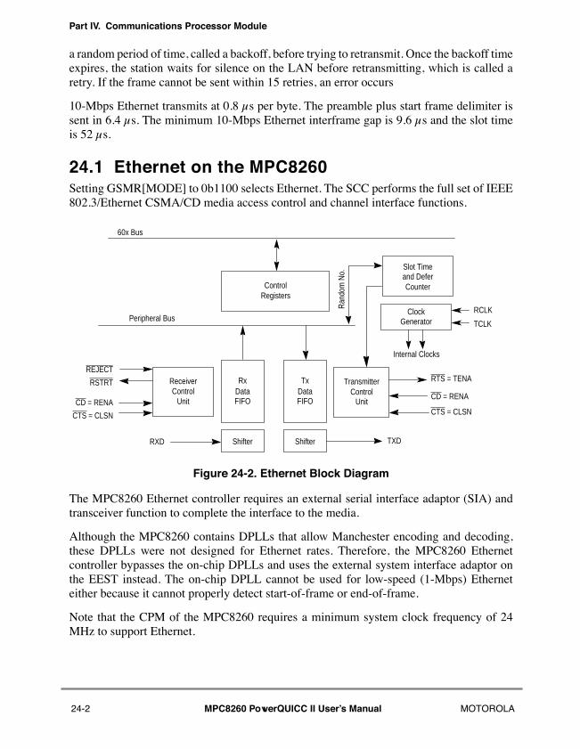
Part IV. Communications Processor Module
a random period of time, called a backoff, before trying to retransmit. Once the backoff timeexpires, the station waits for silence on the LAN before retransmitting, which is called aretry. If the frame cannot be sent within 15 retries, an error occurs
10-Mbps Ethernet transmits at 0.8 µs per byte. The preamble plus start frame delimiter issent in 6.4 µs. The minimum 10-Mbps Ethernet interframe gap is 9.6 µs and the slot timeis 52 µs.
24.1 Ethernet on the MPC8260Setting GSMR[MODE] to 0b1100 selects Ethernet. The SCC performs the full set of IEEE802.3/Ethernet CSMA/CD media access control and channel interface functions.
Figure 24-2. Ethernet Block Diagram
The MPC8260 Ethernet controller requires an external serial interface adaptor (SIA) andtransceiver function to complete the interface to the media.
Although the MPC8260 contains DPLLs that allow Manchester encoding and decoding,these DPLLs were not designed for Ethernet rates. Therefore, the MPC8260 Ethernetcontroller bypasses the on-chip DPLLs and uses the external system interface adaptor onthe EEST instead. The on-chip DPLL cannot be used for low-speed (1-Mbps) Etherneteither because it cannot properly detect start-of-frame or end-of-frame.
Note that the CPM of the MPC8260 requires a minimum system clock frequency of 24MHz to support Ethernet.
Shifter
RxReceiverControl
Unit FIFO
Shifter
Tx TransmitterControl
UnitFIFO
Slot Time
ClockGenerator
Internal Clocks
ControlRegisters
TXDRXD
Peripheral Bus
DataData
RCLK
TCLK
and DeferCounter
RTS = TENA
Ran
dom
No.
CD = RENA
CTS = CLSNCTS = CLSN
CD = RENA
REJECT
RSTRT
60x Bus
24-2 MPC8260 PowerQUICC II UserÕs Manual MOTOROLA
Part IV. Communications Processor Module
24.2 FeaturesThe following list summarizes the main features of the SCC in Ethernet mode:
¥ Performs MAC layer functions of Ethernet and IEEE 802.3
¥ Performs framing functions
Ñ Preamble generation and stripping
Ñ Destination address checking
Ñ CRC generation and checking
Ñ Automatically pads short frames on transmit
Ñ Framing error (dribbling bits) handling
¥ Full collision support
Ñ Enforces the collision (jamming)
Ñ Truncated binary exponential backoff algorithm for random wait
Ñ Two nonaggressive backoff modes
Ñ Automatic frame retransmission (until the attempt limit is reached)
Ñ Automatic discard of incoming collided frames
Ñ Delay transmission of new frames for speciÞed interframe gap
¥ Maximum 10 Mbps bit rate
¥ Optional full-duplex support
¥ Back-to-back frame reception
¥ Detection of receive frames that are too long
¥ Multibuffer data structure
¥ Supports 48-bit addresses in three modes
Ñ PhysicalÐOne 48-bit address recognized or 64-bin hash table for physical addresses
Ñ LogicalÐ64-bin group address hash table plus broadcast address checking
Ñ PromiscuousÐReceives all addresses, but discards frame if REJECT is asserted
¥ External content-addressable memory (CAM) support on serial bus interfaces
¥ Up to eight parallel I/O pins can be sampled and appended to any frame
¥ Optional heartbeat indication
¥ Transmitter network management and diagnostics
Ñ Lost carrier sense
Ñ Underrun
Ñ Number of collisions exceeded the maximum allowed
MOTOROLA Chapter 24. SCC Ethernet Mode 24-3
Part IV. Communications Processor Module
Ñ Number of retries per frame
Ñ Deferred frame indication
Ñ Late collision
¥ Receiver network management and diagnostics
Ñ CRC error indication
Ñ Nonoctet alignment error
Ñ Frame too short
Ñ Frame too long
Ñ Overrun
Ñ Busy (out of buffers)
¥ Error counters
Ñ Discarded frames (out of buffers or overrun occurred)
Ñ CRC errors
Ñ Alignment errors
¥ Internal and external loopback mode
24.3 Connecting the MPC8260 to EthernetThe basic interface to the external SIA chip consists of the following Ethernet signals:
¥ Receive clock (RCLK)Ña CLKx signal routed through the bank of clocks on the MPC8260.
¥ Transmit clock (TCLK)Ña CLKx signal routed through the bank of clocks on the MPC8260. Note that RCLK and TCLK should not be connected to the same CLKx since the SIA provides separate transmit and receive clock signals.
¥ Transmit data (TXD)Ñthe MPC8260 TXD signal.
¥ Receive data (RXD)Ñthe MPC8260 RXD signal.
The following signals take on different functionality when the SCC is in Ethernet mode:
¥ Transmit enable (TENA)ÑRTS becomes TENA. The polarity of TENA is active high, whereas the polarity of RTS is active low.
¥ Receive enable (RENA)ÑCD becomes RENA.
¥ Collision (CLSN)ÑCTS becomes CLSN. The carrier sense signal is referenced in Ethernet descriptions because it indicates when the LAN is in use. Carrier sense is deÞned as the logical OR of RENA and CLSN.
Figure 24-3 shows the basic components and signals required to make an Ethernetconnection between the MPC8260 and EEST.
24-4 MPC8260 PowerQUICC II UserÕs Manual MOTOROLA
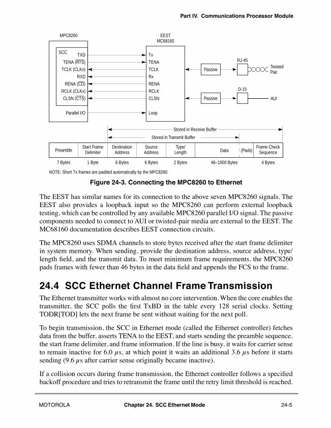
Part IV. Communications Processor Module
Figure 24-3. Connecting the MPC8260 to Ethernet
The EEST has similar names for its connection to the above seven MPC8260 signals. TheEEST also provides a loopback input so the MPC8260 can perform external loopbacktesting, which can be controlled by any available MPC8260 parallel I/O signal. The passivecomponents needed to connect to AUI or twisted-pair media are external to the EEST. TheMC68160 documentation describes EEST connection circuits.
The MPC8260 uses SDMA channels to store bytes received after the start frame delimiterin system memory. When sending, provide the destination address, source address, type/length Þeld, and the transmit data. To meet minimum frame requirements, the MPC8260pads frames with fewer than 46 bytes in the data Þeld and appends the FCS to the frame.
24.4 SCC Ethernet Channel Frame Transmission The Ethernet transmitter works with almost no core intervention. When the core enables thetransmitter, the SCC polls the Þrst TxBD in the table every 128 serial clocks. SettingTODR[TOD] lets the next frame be sent without waiting for the next poll.
To begin transmission, the SCC in Ethernet mode (called the Ethernet controller) fetchesdata from the buffer, asserts TENA to the EEST, and starts sending the preamble sequence,the start frame delimiter, and frame information. If the line is busy, it waits for carrier senseto remain inactive for 6.0 µs, at which point it waits an additional 3.6 µs before it startssending (9.6 µs after carrier sense originally became inactive).
If a collision occurs during frame transmission, the Ethernet controller follows a speciÞedbackoff procedure and tries to retransmit the frame until the retry limit threshold is reached.
MPC8260 EESTMC68160
TXD
TENA (RTS)
TCLK (CLKx)
RXD
RENA (CD)
RCLK (CLKx)
CLSN (CTS)
Parallel I/O
Tx
TENA
TCLK
Rx
RENA
RCLK
CLSN
Loop
Passive
Passive
TwistedPair
AUI
PreambleStart Frame
DataDelimiterDestination
AddressType/
LengthSourceAddress
Frame CheckSequence
7 Bytes 1 Byte 6 Bytes 6 Bytes 2 Bytes 46–1500 Bytes 4 Bytes
Stored in Receive Buffer
RJ-45
D-15
Stored in Transmit Buffer
SCC
NOTE: Short Tx frames are padded automatically by the MPC8260.
(Pads)
MOTOROLA Chapter 24. SCC Ethernet Mode 24-5
Part IV. Communications Processor Module
The Ethernet controller stores the Þrst 5 to 8 bytes of the transmit frame in dual-port RAMso they need not be retrieved from system memory in case of a collision. This improves bususage and latency when the backoff timer output requires an immediate retransmission. Ifa collision occurs during frame transmission, the controller returns to the Þrst buffer for aretransmission. The only restriction is that the Þrst buffer must contain at least 9 bytes.
Note that if an Ethernet frame consists of multiple buffers, do not reuse the Þrst BD untilthe CPM clears the R bit of the last BD.
When the end of the current BD is reached and TxBD[L] is set, the FCS bytes are appended(if the TC bit is set in the TxBD), and TENA is negated. This notiÞes the EEST of the needto generate the illegal Manchester encoding that marks the end of an Ethernet frame. AfterCRC transmission, the Ethernet controller writes the frame status bits into the BD andclears the R bit. When the end of the current BD is reached and the L bit is not set, only theR bit is cleared.
In either mode, whether an interrupt is issued depends on how the I bit is set in the TxBD.The Ethernet controller proceeds to the next TxBD. Transmission can be interrupted aftereach frame, after each buffer, or after a speciÞc buffer is sent. The Ethernet controller canpad characters to short frames. If TxBD[PAD] is set, the frame is padded up to the value ofthe minimum frame length register (MINFLR).
To send expedited data before previously linked buffers or for error situations, theGRACEFUL STOP TRANSMIT command can be used to rearrange transmit queue before theCPM sends all the frames; the Ethernet controller stops immediately if no transmission isin progress or it will keep sending until the current frame either Þnishes or terminates witha collision. When the Ethernet controller receives a RESTART TRANSMIT command, itresumes transmission. The Ethernet controller sends bytes least-signiÞcant bit Þrst.
24.5 SCC Ethernet Channel Frame Reception The Ethernet receiver handles address recognition and performs CRC, short frame,maximum DMA transfer, and maximum frame length checking with almost no coreintervention. When the core enables the Ethernet receiver, it enters hunt mode as soon asRENA is asserted while CLSN is negated. In hunt mode, as data is shifted into the receiveshift register one bit at a time, the register contents are compared to the contents of theSYN1 Þeld in the data synchronization register (DSR). This compare function becomesvalid a certain number of clocks after the start of the frame (depending on PSMR[NIB]). Ifthe two are not equal, the next bit is shifted in and the comparison is repeated. If a double-zero or double-one fault is detected between bits 14 to 21 from the Þrst received preamblebit, the frame is rejected. If a double-zero fault is detected after 21 bits from the Þrstreceived preamble bit and before detection of the start frame delimiter (SFD), the frame isalso rejected. When the incoming pattern is not rejected and matches the DSR, the SFD hasbeen detected; hunt mode is terminated and character assembly begins.
When the receiver detects the Þrst bytes of the frame, the Ethernet controller performs
24-6 MPC8260 PowerQUICC II UserÕs Manual MOTOROLA
Part IV. Communications Processor Module
address recognition on the frame. The receiver can receive physical (individual), group(multicast), and broadcast addresses. Ethernet receive frame data is not written to memoryuntil the internal address recognition process completes, which improves bus usage withframes not addressed to this station.
If a match is found, the Ethernet controller fetches the next RxBD and, if it is empty, startstransferring the incoming frame to the RxBD associated data buffer. If a collision isdetected during the frame, the RxBDs associated with this frame are reused. Thus, therewill be no collision frames presented to you except late collisions, which indicate seriousLAN problems. When the data buffer has been Þlled, the Ethernet controller clears the Ebit in the RxBD and generates an interrupt if the I bit is set. If the incoming frame exceedsthe length of the data buffer, the Ethernet controller fetches the next RxBD in the table and,if it is empty, continues transferring the rest of the frame to this buffer. The RxBD length isdetermined by MRBLR in the SCC general-purpose parameter RAM, which should be atleast 64 bytes.
During reception, the Ethernet controller checks for a frame that is either too short or toolong. When the frame ends, the receive CRC Þeld is checked and written to the buffer. Thedata length written to the last BD in the Ethernet frame is the length of the entire frame andit enables the software to correctly recognize the frame-too-long condition.
The Ethernet controller then sets the L bit in the RxBD, writes the other frame status bitsinto the RxBD, and clears the E bit. Then it generates a maskable interrupt, which indicatesthat a frame has been received and is in memory. The Ethernet controller then waits for anew frame. It receives serial data least-signiÞcant bit Þrst.
24.6 The Content-Addressable Memory (CAM) Interface
The Ethernet controller has one option for connecting to an external CAMÑa serialinterface. The reject signal (REJECT) is used to signify that the current frame should bediscarded. The MPC8260Õs internal address recognition logic can be used in combinationwith an external CAM. See Section 24.10, ÒSCC Ethernet Address Recognition.Ó
The MPC8260 outputs a receive start (RSTRT) signal when the start frame delimiter isrecognized. This signal is asserted for one bit time on the second destination address bit.The CAM control logic uses RSTRT (in combination with the RXD and RCLK signals) tostore the destination or source address and generate writes to the CAM for addressrecognition. In addition, the RENA signal supplied from the SIA can be used to abort thecomparison if a collision occurs on the receive frame.
After the comparison, the CAM control logic asserts the receive reject signal (REJECT), ifthe current receive frame is rejected. The MPC8260Õs Ethernet controller then immediatelystops writing data to system memory and reuses the buffer(s) for the next frame. If the CAMaccepts the frame, the CAM control logic does nothing (REJECT is not asserted). However,if REJECT is asserted, it must be done prior to the end of the receive frame.
MOTOROLA Chapter 24. SCC Ethernet Mode 24-7
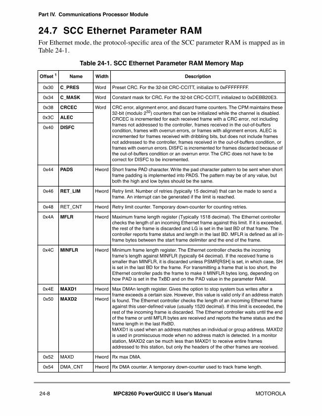
Part IV. Communications Processor Module
24.7 SCC Ethernet Parameter RAMFor Ethernet mode, the protocol-speciÞc area of the SCC parameter RAM is mapped as inTable 24-1.
Table 24-1. SCC Ethernet Parameter RAM Memory Map
Offset 1 Name Width Description
0x30 C_PRES Word Preset CRC. For the 32-bit CRC-CCITT, initialize to 0xFFFFFFFF.
0x34 C_MASK Word Constant mask for CRC. For the 32-bit CRC-CCITT, initialized to 0xDEBB20E3.
0x38 CRCEC Word CRC error, alignment error, and discard frame counters. The CPM maintains these 32-bit (modulo 232) counters that can be initialized while the channel is disabled. CRCEC is incremented for each received frame with a CRC error, not including frames not addressed to the controller, frames received in the out-of-buffers condition, frames with overrun errors, or frames with alignment errors. ALEC is incremented for frames received with dribbling bits, but does not include frames not addressed to the controller, frames received in the out-of-buffers condition, or frames with overrun errors. DISFC is incremented for frames discarded because of the out-of-buffers condition or an overrun error. The CRC does not have to be correct for DISFC to be incremented.
0x3C ALEC
0x40 DISFC
0x44 PADS Hword Short frame PAD character. Write the pad character pattern to be sent when short frame padding is implemented into PADS. The pattern may be of any value, but both the high and low bytes should be the same.
0x46 RET_LIM Hword Retry limit. Number of retries (typically 15 decimal) that can be made to send a frame. An interrupt can be generated if the limit is reached.
0x48 RET_CNT Hword Retry limit counter. Temporary down-counter for counting retries.
0x4A MFLR Hword Maximum frame length register (Typically 1518 decimal). The Ethernet controller checks the length of an incoming Ethernet frame against this limit. If it is exceeded, the rest of the frame is discarded and LG is set in the last BD of that frame. The controller reports frame status and length in the last BD. MFLR is defined as all in-frame bytes between the start frame delimiter and the end of the frame.
0x4C MINFLR Hword Minimum frame length register. The Ethernet controller checks the incoming frameÕs length against MINFLR (typically 64 decimal). If the received frame is smaller than MINFLR, it is discarded unless PSMR[RSH] is set, in which case, SH is set in the last BD for the frame. For transmitting a frame that is too short, the Ethernet controller pads the frame to make it MINFLR bytes long, depending on how PAD is set in the TxBD and on the PAD value in the parameter RAM.
0x4E MAXD1 Hword Max DMAn length register. Gives the option to stop system bus writes after a frame exceeds a certain size. However, this value is valid only if an address match is found. The Ethernet controller checks the length of an incoming Ethernet frame against this user-defined value (usually 1520 decimal). If this limit is exceeded, the rest of the incoming frame is discarded. The Ethernet controller waits until the end of the frame or until MFLR bytes are received and reports the frame status and the frame length in the last RxBD. MAXD1 is used when an address matches an individual or group address. MAXD2 is used in promiscuous mode when no address match is detected. In a monitor station, MAXD2 can be much less than MAXD1 to receive entire frames addressed to this station, but only the headers of the other frames are received.
0x50 MAXD2 Hword
0x52 MAXD Hword Rx max DMA.
0x54 DMA_CNT Hword Rx DMA counter. A temporary down-counter used to track frame length.
24-8 MPC8260 PowerQUICC II UserÕs Manual MOTOROLA
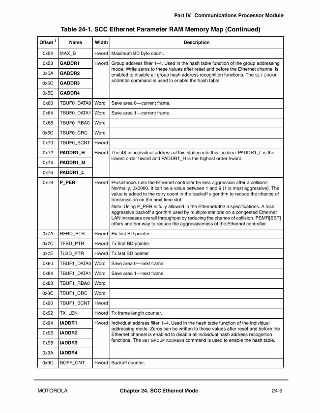
Part IV. Communications Processor Module
0x54 MAX_B Hword Maximum BD byte count.
0x58 GADDR1 Hword Group address Þlter 1Ð4. Used in the hash table function of the group addressing mode. Write zeros to these values after reset and before the Ethernet channel is enabled to disable all group hash address recognition functions. The SET GROUP ADDRESS command is used to enable the hash table.
0x5A GADDR2
0x5C GADDR3
0x5E GADDR4
0x60 TBUF0_DATA0 Word Save area 0Ñcurrent frame.
0x64 TBUF0_DATA1 Word Save area 1Ñcurrent frame.
0x68 TBUF0_RBA0 Word
0x6C TBUF0_CRC Word
0x70 TBUF0_BCNT Hword
0x72 PADDR1_H Hword The 48-bit individual address of this station into this location. PADDR1_L is the lowest order hword and PADDR1_H is the highest order hword.
0x74 PADDR1_M
0x76 PADDR1_L
0x78 P_PER Hword Persistence. Lets the Ethernet controller be less aggressive after a collision. Normally, 0x0000. It can be a value between 1 and 9 (1 is most aggressive). The value is added to the retry count in the backoff algorithm to reduce the chance of transmission on the next time slot.Note: Using P_PER is fully allowed in the Ethernet/802.3 specifications. A less aggressive backoff algorithm used by multiple stations on a congested Ethernet LAN increases overall throughput by reducing the chance of collision. PSMR[SBT] offers another way to reduce the aggressiveness of the Ethernet controller.
0x7A RFBD_PTR Hword Rx Þrst BD pointer.
0x7C TFBD_PTR Hword Tx Þrst BD pointer.
0x7E TLBD_PTR Hword Tx last BD pointer.
0x80 TBUF1_DATA0 Word Save area 0Ñnext frame.
0x84 TBUF1_DATA1 Word Save area 1Ñnext frame.
0x88 TBUF1_RBA0 Word
0x8C TBUF1_CRC Word
0x90 TBUF1_BCNT Hword
0x92 TX_LEN Hword Tx frame length counter.
0x94 IADDR1 Hword Individual address Þlter 1Ð4. Used in the hash table function of the individual addressing mode. Zeros can be written to these values after reset and before the Ethernet channel is enabled to disable all individual hash address recognition functions. The SET GROUP ADDRESS command is used to enable the hash table.
0x96 IADDR2
0x98 IADDR3
0x9A IADDR4
0x9C BOFF_CNT Hword Backoff counter.
Table 24-1. SCC Ethernet Parameter RAM Memory Map (Continued)
Offset 1 Name Width Description
MOTOROLA Chapter 24. SCC Ethernet Mode 24-9
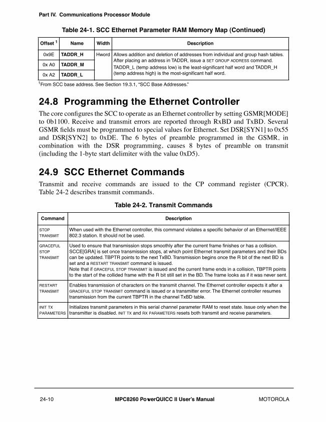
Part IV. Communications Processor Module
24.8 Programming the Ethernet ControllerThe core conÞgures the SCC to operate as an Ethernet controller by setting GSMR[MODE]to 0b1100. Receive and transmit errors are reported through RxBD and TxBD. SeveralGSMR Þelds must be programmed to special values for Ethernet. Set DSR[SYN1] to 0x55and DSR[SYN2] to 0xDE. The 6 bytes of preamble programmed in the GSMR, incombination with the DSR programming, causes 8 bytes of preamble on transmit(including the 1-byte start delimiter with the value 0xD5).
24.9 SCC Ethernet CommandsTransmit and receive commands are issued to the CP command register (CPCR).Table 24-2 describes transmit commands.
0x9E TADDR_H Hword Allows addition and deletion of addresses from individual and group hash tables. After placing an address in TADDR, issue a SET GROUP ADDRESS command. TADDR_L (temp address low) is the least-signiÞcant half word and TADDR_H (temp address high) is the most-signiÞcant half word.
0x A0 TADDR_M
0x A2 TADDR_L
1From SCC base address. See Section 19.3.1, ÒSCC Base Addresses.Ó
Table 24-2. Transmit Commands
Command Description
STOP TRANSMIT
When used with the Ethernet controller, this command violates a speciÞc behavior of an Ethernet/IEEE 802.3 station. It should not be used.
GRACEFUL STOP TRANSMIT
Used to ensure that transmission stops smoothly after the current frame Þnishes or has a collision. SCCE[GRA] is set once transmission stops, at which point Ethernet transmit parameters and their BDs can be updated. TBPTR points to the next TxBD. Transmission begins once the R bit of the next BD is set and a RESTART TRANSMIT command is issued.Note that if GRACEFUL STOP TRANSMIT is issued and the current frame ends in a collision, TBPTR points to the start of the collided frame with the R bit still set in the BD. The frame looks as if it was never sent.
RESTART TRANSMIT
Enables transmission of characters on the transmit channel. The Ethernet controller expects it after a GRACEFUL STOP TRANSMIT command is issued or a transmitter error. The Ethernet controller resumes transmission from the current TBPTR in the channel TxBD table.
INIT TX PARAMETERS
Initializes transmit parameters in this serial channel parameter RAM to reset state. Issue only when the transmitter is disabled. INIT TX and RX PARAMETERS resets both transmit and receive parameters.
Table 24-1. SCC Ethernet Parameter RAM Memory Map (Continued)
Offset 1 Name Width Description
24-10 MPC8260 PowerQUICC II UserÕs Manual MOTOROLA
Part IV. Communications Processor Module
Table 24-3 describes receive commands.
Note that after a CPM reset via CPCR[RST], the Ethernet transmit enable (TENA) signaldefaults to its RTS, active-low functionality. To prevent false TENA assertions to anexternal transceiver, conÞgure TENA as an input before issuing a CPM reset. See step 3 inSection 24.21, ÒSCC Ethernet Programming Example.Ó
24.10 SCC Ethernet Address RecognitionThe Ethernet controller can Þlter received frames based on different addressing typesÑphysical (individual), group (multicast), broadcast (all-ones group address), andpromiscuous. The difference between an individual address and a group address isdetermined by the I/G bit in the destination address Þeld. A ßowchart for addressrecognition on received frames is shown in Figure 24-4.
In the physical type of address recognition, the Ethernet controller compares the destinationaddress Þeld of the received frame with the user-programmed physical address in PADDR1.Address recognition can be performed on multiple individual addresses using theIADDR1Ð4 hash table.
Table 24-3. Receive Commands
Command Description
ENTER HUNT MODE
After hardware or software is reset and the channel is enabled in GSMR_L, the channel is in receive enable mode and uses the Þrst BD in the table. The receiver then enters hunt mode, waiting for an incoming frame. The ENTER HUNT MODE command is generally used to force the Ethernet receiver to stop receiving the current frame and enter hunt mode, in which the Ethernet controller continually scans the input data stream for a transition of carrier sense from inactive to active and then a preamble sequence followed by the start frame delimiter. After receiving the command, the buffer is closed and the CRC calculation is reset. The next RxBD is used to receive more frames.
CLOSE RXBD Should not be used with the Ethernet controller.
INIT RX PARAMETERS
Initializes receive parameters in this serial channel parameter RAM to their reset state. Issue it only when the receiver is disabled. INIT TX and RX PARAMETERS resets receive and transmit parameters.
SET GROUP ADDRESS
Used to set one of the 64 bits of the four individual/group address hash Þlter registers. The address to be added to the hash table should be written to TADDR_L, TADDR_M, and TADDR_H in the parameter RAM before executing this command. The CP uses an individual address if the I/G bit in the address stored in TADDR is 0; otherwise, it uses a group address. This command can be executed at any time, regardless of whether the Ethernet channel is enabled.To delete an address from the hash table, disable the Ethernet channel, clear the hash table registers, and execute this command for the remaining addresses. Do not simply clear the channelÕs associated hash table bit because the hash table may have multiple addresses mapped to the same hash table bit.
MOTOROLA Chapter 24. SCC Ethernet Mode 24-11
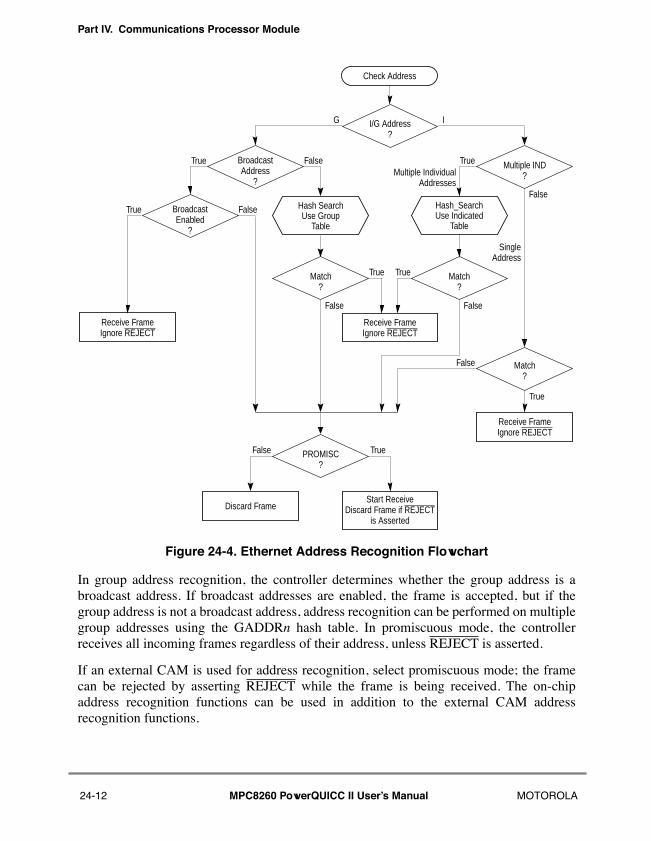
Part IV. Communications Processor Module
Figure 24-4. Ethernet Address Recognition Flowchart
In group address recognition, the controller determines whether the group address is abroadcast address. If broadcast addresses are enabled, the frame is accepted, but if thegroup address is not a broadcast address, address recognition can be performed on multiplegroup addresses using the GADDRn hash table. In promiscuous mode, the controllerreceives all incoming frames regardless of their address, unless REJECT is asserted.
If an external CAM is used for address recognition, select promiscuous mode; the framecan be rejected by asserting REJECT while the frame is being received. The on-chipaddress recognition functions can be used in addition to the external CAM addressrecognition functions.
Check Address
I/G Address?
Hash_SearchFalse
G
True
True
Multiple IND?
BroadcastAddress
Use IndicatedTable
Hash SearchUse Group
Table
Match?
Match?
Receive FrameIgnore REJECT
Receive FrameIgnore REJECT
Match?
Receive FrameIgnore REJECT
PROMISC?
Start ReceiveDiscard Frame if REJECTDiscard Frame
is Asserted
I
True
True
False
False True
True
FalseFalse
?
BroadcastEnabled
?
True False
False
Multiple IndividualAddresses
SingleAddress
24-12 MPC8260 PowerQUICC II UserÕs Manual MOTOROLA
Part IV. Communications Processor Module
If the external CAM stores addresses that should be rejected rather than accepted, the useof REJECT by the CAM should be logically inverted.
24.11 Hash Table AlgorithmIndividual and group hash Þltering operate using certain processes. The Ethernet controllermaps any 48-bit address into one of 64 bins, each represented by a bit stored in GADDRxor IADDRx. When a SET GROUP ADDRESS command is executed, the Ethernet controllermaps the selected 48-bit address into one of the 64 bits by passing the 48-bit addressthrough the on-chip 32-bit CRC generator and selecting 6 bits of the CRC-encoded resultto generate a number between 1 and 64. Bits 31Ð30 of the CRC result select one of theGADDRs or IADDRs; bits 29Ð26 of the CRC result indicate the bit in that register.
When the Ethernet controller receives a frame, the same process is used. If the CRCgenerator selects a bit that is set in the group/individual hash table, the frame is accepted.Otherwise, it is rejected. So, if eight group addresses are stored in the hash table andrandom group addresses are received, the hash table prevents roughly 56/64 (87.5%) of thegroup address frames from reaching memory. Frames that reach memory must be furtherÞltered by the processor to determine if they contain one of the eight preferred addresses.
Better performance is achieved by using the group and individual hash tablessimultaneously. For instance, if eight group and eight physical addresses are stored in theirrespective hash tables, 87.5% of all frames are prevented from reaching memory. Theeffectiveness of the hash table declines as the number of addresses increases. For instance,with 128 addresses stored in a 64-bin hash table, the vast majority of the hash table bits areset, thus preventing a small fraction of the frames from reaching memory.
Hash tables cannot be used to reject frames that match a set of entered addresses becauseunintended addresses are mapped to the same bit in the hash table.
24.12 Interpacket Gap TimeThe receiver receives back-to-back frames with a minimum interpacket spacing of 9.6 µs.In addition, after the backoff algorithm, the transmitter waits for carrier sense to be negatedbefore resending the frame. Retransmission begins 9.6 µs after carrier sense is negated if itstays negated for at least 6.4 µs.
24.13 Handling CollisionsIf a collision occurs as a frame is being sent, the Ethernet controller continues sending forat least 32 bit times, thus sending a JAM pattern of 32 ones. If a collision occurs during thepreamble sequence, the JAM pattern is sent at the end of the sequence.
If a collision occurs within 64 byte times, the retry process is initiated. The transmitter waitsa random number of slot times (512 bit times or 52 µs). If a collision occurs after 64 bytetimes, no retransmission is performed and the buffer is closed with an LC error indication.
MOTOROLA Chapter 24. SCC Ethernet Mode 24-13
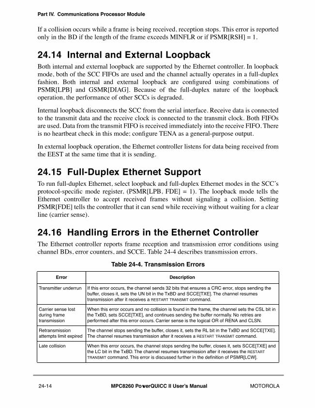
Part IV. Communications Processor Module
If a collision occurs while a frame is being received, reception stops. This error is reportedonly in the BD if the length of the frame exceeds MINFLR or if PSMR[RSH] = 1.
24.14 Internal and External LoopbackBoth internal and external loopback are supported by the Ethernet controller. In loopbackmode, both of the SCC FIFOs are used and the channel actually operates in a full-duplexfashion. Both internal and external loopback are conÞgured using combinations ofPSMR[LPB] and GSMR[DIAG]. Because of the full-duplex nature of the loopbackoperation, the performance of other SCCs is degraded.
Internal loopback disconnects the SCC from the serial interface. Receive data is connectedto the transmit data and the receive clock is connected to the transmit clock. Both FIFOsare used. Data from the transmit FIFO is received immediately into the receive FIFO. Thereis no heartbeat check in this mode; conÞgure TENA as a general-purpose output.
In external loopback operation, the Ethernet controller listens for data being received fromthe EEST at the same time that it is sending.
24.15 Full-Duplex Ethernet SupportTo run full-duplex Ethernet, select loopback and full-duplex Ethernet modes in the SCCÕsprotocol-speciÞc mode register, (PSMR[LPB, FDE] = 1). The loopback mode tells theEthernet controller to accept received frames without signaling a collision. SettingPSMR[FDE] tells the controller that it can send while receiving without waiting for a clearline (carrier sense).
24.16 Handling Errors in the Ethernet ControllerThe Ethernet controller reports frame reception and transmission error conditions usingchannel BDs, error counters, and SCCE. Table 24-4 describes transmission errors.
Table 24-4. Transmission Errors
Error Description
Transmitter underrun If this error occurs, the channel sends 32 bits that ensures a CRC error, stops sending the buffer, closes it, sets the UN bit in the TxBD and SCCE[TXE]. The channel resumes transmission after it receives a RESTART TRANSMIT command.
Carrier sense lost during frame transmission
When this error occurs and no collision is found in the frame, the channel sets the CSL bit in the TxBD, sets SCCE[TXE], and continues sending the buffer normally. No retries are performed after this error occurs. Carrier sense is the logical OR of RENA and CLSN.
Retransmission attempts limit expired
The channel stops sending the buffer, closes it, sets the RL bit in the TxBD and SCCE[TXE]. The channel resumes transmission after it receives a RESTART TRANSMIT command.
Late collision When this error occurs, the channel stops sending the buffer, closes it, sets SCCE[TXE] and the LC bit in the TxBD. The channel resumes transmission after it receives the RESTART TRANSMIT command. This error is discussed further in the deÞnition of PSMR[LCW].
24-14 MPC8260 PowerQUICC II UserÕs Manual MOTOROLA
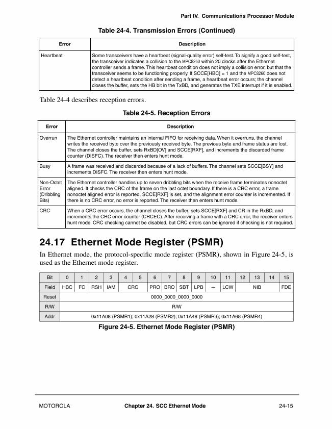
Part IV. Communications Processor Module
Table 24-4 describes reception errors.
24.17 Ethernet Mode Register (PSMR)In Ethernet mode, the protocol-speciÞc mode register (PSMR), shown in Figure 24-5, isused as the Ethernet mode register.
Heartbeat Some transceivers have a heartbeat (signal-quality error) self-test. To signify a good self-test, the transceiver indicates a collision to the MPC8260 within 20 clocks after the Ethernet controller sends a frame. This heartbeat condition does not imply a collision error, but that the transceiver seems to be functioning properly. If SCCE[HBC] = 1 and the MPC8260 does not detect a heartbeat condition after sending a frame, a heartbeat error occurs; the channel closes the buffer, sets the HB bit in the TxBD, and generates the TXE interrupt if it is enabled.
Table 24-5. Reception Errors
Error Description
Overrun The Ethernet controller maintains an internal FIFO for receiving data. When it overruns, the channel writes the received byte over the previously received byte. The previous byte and frame status are lost. The channel closes the buffer, sets RxBD[OV] and SCCE[RXF], and increments the discarded frame counter (DISFC). The receiver then enters hunt mode.
Busy A frame was received and discarded because of a lack of buffers. The channel sets SCCE[BSY] and increments DISFC. The receiver then enters hunt mode.
Non-Octet Error (Dribbling Bits)
The Ethernet controller handles up to seven dribbling bits when the receive frame terminates nonoctet aligned. It checks the CRC of the frame on the last octet boundary. If there is a CRC error, a frame nonoctet aligned error is reported, SCCE[RXF] is set, and the alignment error counter is incremented. If there is no CRC error, no error is reported. The receiver then enters hunt mode.
CRC When a CRC error occurs, the channel closes the buffer, sets SCCE[RXF] and CR in the RxBD, and increments the CRC error counter (CRCEC). After receiving a frame with a CRC error, the receiver enters hunt mode. CRC checking cannot be disabled, but CRC errors can be ignored if checking is not required.
Bit 0 1 2 3 4 5 6 7 8 9 10 11 12 13 14 15
Field HBC FC RSH IAM CRC PRO BRO SBT LPB Ñ LCW NIB FDE
Reset 0000_0000_0000_0000
R/W R/W
Addr 0x11A08 (PSMR1); 0x11A28 (PSMR2); 0x11A48 (PSMR3); 0x11A68 (PSMR4)
Figure 24-5. Ethernet Mode Register (PSMR)
Table 24-4. Transmission Errors (Continued)
Error Description
MOTOROLA Chapter 24. SCC Ethernet Mode 24-15
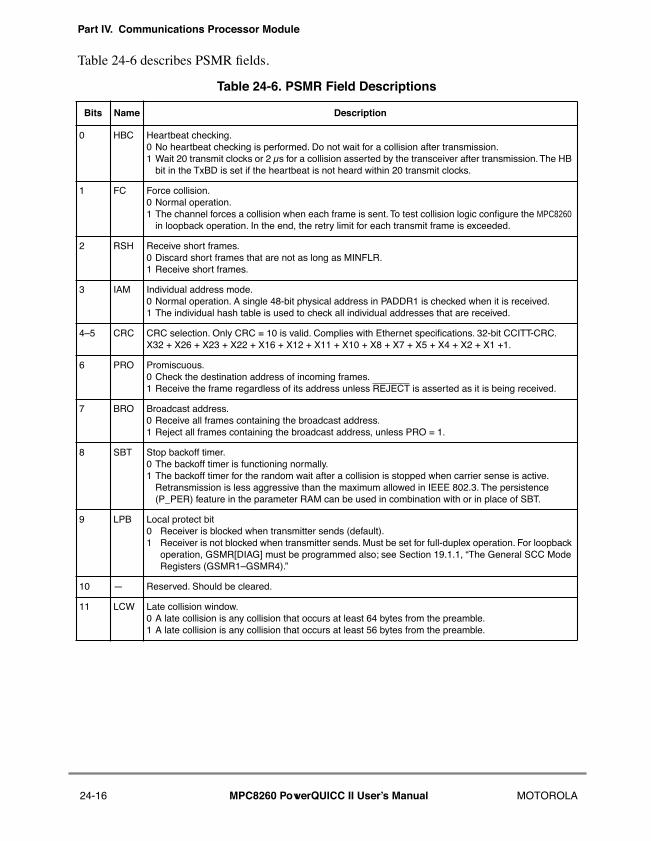
Part IV. Communications Processor Module
Table 24-6 describes PSMR Þelds.
Table 24-6. PSMR Field Descriptions
Bits Name Description
0 HBC Heartbeat checking. 0 No heartbeat checking is performed. Do not wait for a collision after transmission.1 Wait 20 transmit clocks or 2 µs for a collision asserted by the transceiver after transmission. The HB
bit in the TxBD is set if the heartbeat is not heard within 20 transmit clocks.
1 FC Force collision. 0 Normal operation.1 The channel forces a collision when each frame is sent. To test collision logic conÞgure the MPC8260
in loopback operation. In the end, the retry limit for each transmit frame is exceeded.
2 RSH Receive short frames. 0 Discard short frames that are not as long as MINFLR.1 Receive short frames.
3 IAM Individual address mode. 0 Normal operation. A single 48-bit physical address in PADDR1 is checked when it is received.1 The individual hash table is used to check all individual addresses that are received.
4Ð5 CRC CRC selection. Only CRC = 10 is valid. Complies with Ethernet speciÞcations. 32-bit CCITT-CRC. X32 + X26 + X23 + X22 + X16 + X12 + X11 + X10 + X8 + X7 + X5 + X4 + X2 + X1 +1.
6 PRO Promiscuous. 0 Check the destination address of incoming frames.1 Receive the frame regardless of its address unless REJECT is asserted as it is being received.
7 BRO Broadcast address. 0 Receive all frames containing the broadcast address.1 Reject all frames containing the broadcast address, unless PRO = 1.
8 SBT Stop backoff timer. 0 The backoff timer is functioning normally.1 The backoff timer for the random wait after a collision is stopped when carrier sense is active.
Retransmission is less aggressive than the maximum allowed in IEEE 802.3. The persistence (P_PER) feature in the parameter RAM can be used in combination with or in place of SBT.
9 LPB Local protect bit0 Receiver is blocked when transmitter sends (default).1 Receiver is not blocked when transmitter sends. Must be set for full-duplex operation. For loopback
operation, GSMR[DIAG] must be programmed also; see Section 19.1.1, ÒThe General SCC Mode Registers (GSMR1ÐGSMR4).Ó
10 Ñ Reserved. Should be cleared.
11 LCW Late collision window. 0 A late collision is any collision that occurs at least 64 bytes from the preamble.1 A late collision is any collision that occurs at least 56 bytes from the preamble.
24-16 MPC8260 PowerQUICC II UserÕs Manual MOTOROLA
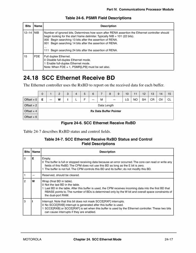
Part IV. Communications Processor Module
24.18 SCC Ethernet Receive BDThe Ethernet controller uses the RxBD to report on the received data for each buffer.
Table 24-7 describes RxBD status and control Þelds.
12Ð14 NIB Number of ignored bits. Determines how soon after RENA assertion the Ethernet controller should begin looking for the start frame delimiter. Typically NIB = 101 (22 bits).000 Begin searching 13 bits after the assertion of RENA.001 Begin searching 14 bits after the assertion of RENA....111 Begin searching 24 bits after the assertion of RENA.
15 FDE Full duplex Ethernet. 0 Disable full-duplex Ethernet mode.1 Enable full-duplex Ethernet mode.Note: When FDE = 1, PSMR[LPB] must be set also.
0 1 2 3 4 5 6 7 8 9 10 11 12 13 14 15
Offset + 0 E Ñ W I L F Ñ M Ñ LG NO SH CR OV CL
Offset + 2 Data Length
Offset + 4 Rx Data Buffer Pointer
Offset + 6
Figure 24-6. SCC Ethernet Receive RxBD
Table 24-7. SCC Ethernet Receive RxBD Status and ControlField Descriptions
Bits Name Description
0 E Empty. 0 The buffer is full or stopped receiving data because an error occurred. The core can read or write any
Þelds of this RxBD. The CPM does not use this BD as long as the E bit is zero.1 The buffer is not full. The CPM controls this BD and its buffer; do not modify this BD.
1 Ñ Reserved, should be cleared.
2 W Wrap (Þnal BD in table). 0 Not the last BD in the table. 1 Last BD in the table. After this buffer is used, the CPM receives incoming data into the Þrst BD that
RBASE points to. The number of BDs is determined only by the W bit and overall space constraints of the dual-port RAM.
3 I Interrupt. Note that this bit does not mask SCCE[RXF] interrupts.0 No SCCE[RXB] interrupt is generated after this buffer is used. 1 SCCE[RXB] or SCCE[RXF] is set when this buffer is used by the Ethernet controller. These two bits
can cause interrupts if they are enabled.
Table 24-6. PSMR Field Descriptions
Bits Name Description
MOTOROLA Chapter 24. SCC Ethernet Mode 24-17
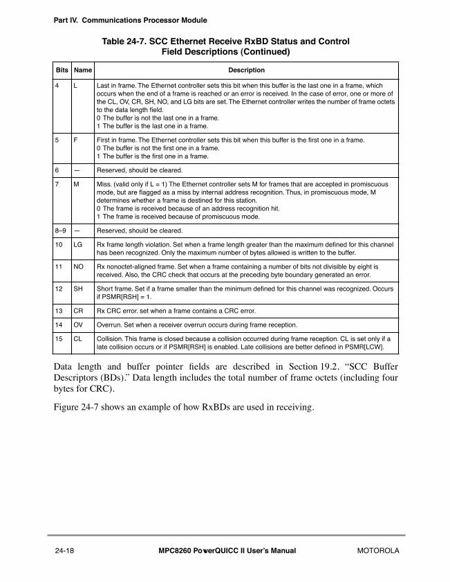
Part IV. Communications Processor Module
Data length and buffer pointer Þelds are described in Section 19.2, ÒSCC BufferDescriptors (BDs).Ó Data length includes the total number of frame octets (including fourbytes for CRC).
Figure 24-7 shows an example of how RxBDs are used in receiving.
4 L Last in frame. The Ethernet controller sets this bit when this buffer is the last one in a frame, which occurs when the end of a frame is reached or an error is received. In the case of error, one or more of the CL, OV, CR, SH, NO, and LG bits are set. The Ethernet controller writes the number of frame octets to the data length Þeld. 0 The buffer is not the last one in a frame. 1 The buffer is the last one in a frame.
5 F First in frame. The Ethernet controller sets this bit when this buffer is the Þrst one in a frame. 0 The buffer is not the Þrst one in a frame. 1 The buffer is the Þrst one in a frame.
6 Ñ Reserved, should be cleared.
7 M Miss. (valid only if L = 1) The Ethernet controller sets M for frames that are accepted in promiscuous mode, but are ßagged as a miss by internal address recognition. Thus, in promiscuous mode, M determines whether a frame is destined for this station. 0 The frame is received because of an address recognition hit.1 The frame is received because of promiscuous mode.
8Ð9 Ñ Reserved, should be cleared.
10 LG Rx frame length violation. Set when a frame length greater than the maximum deÞned for this channel has been recognized. Only the maximum number of bytes allowed is written to the buffer.
11 NO Rx nonoctet-aligned frame. Set when a frame containing a number of bits not divisible by eight is received. Also, the CRC check that occurs at the preceding byte boundary generated an error.
12 SH Short frame. Set if a frame smaller than the minimum deÞned for this channel was recognized. Occurs if PSMR[RSH] = 1.
13 CR Rx CRC error. set when a frame contains a CRC error.
14 OV Overrun. Set when a receiver overrun occurs during frame reception.
15 CL Collision. This frame is closed because a collision occurred during frame reception. CL is set only if a late collision occurs or if PSMR[RSH] is enabled. Late collisions are better deÞned in PSMR[LCW].
Table 24-7. SCC Ethernet Receive RxBD Status and ControlField Descriptions (Continued)
Bits Name Description
24-18 MPC8260 PowerQUICC II UserÕs Manual MOTOROLA
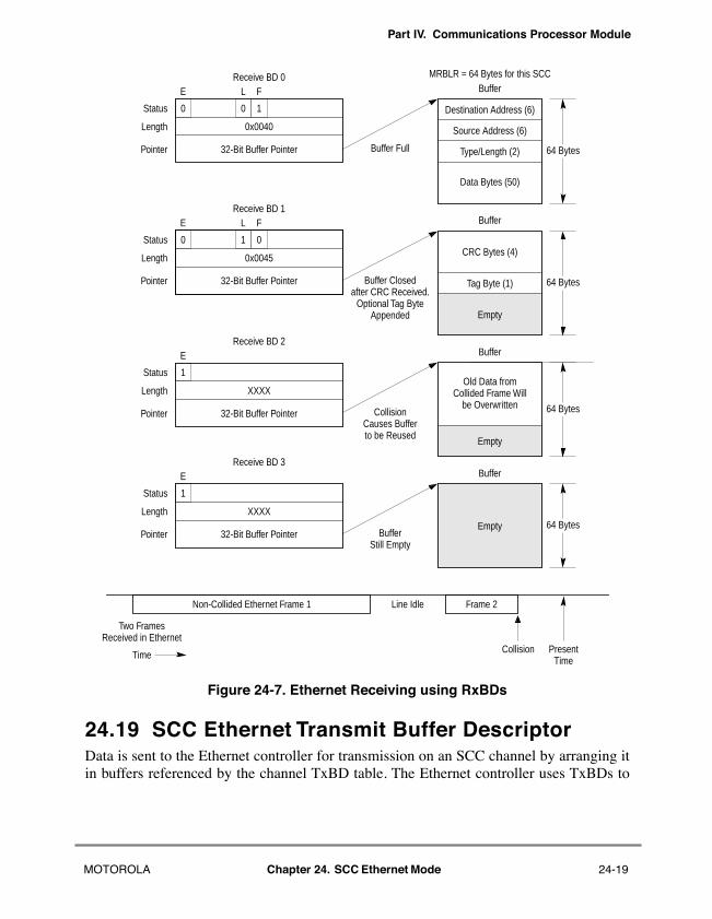
Part IV. Communications Processor Module
Figure 24-7. Ethernet Receiving using RxBDs
24.19 SCC Ethernet Transmit Buffer DescriptorData is sent to the Ethernet controller for transmission on an SCC channel by arranging itin buffers referenced by the channel TxBD table. The Ethernet controller uses TxBDs to
Buffer
0
0x0040
32-Bit Buffer Pointer
1
E FReceive BD 0
Status
Length
Pointer
0
0x0045
32-Bit Buffer Pointer
0
E FReceive BD 1
Status
Length
Pointer
1
XXXX
32-Bit Buffer Pointer
EReceive BD 2
Status
Length
Pointer
1
XXXX
32-Bit Buffer Pointer
EReceive BD 3
Status
Length
Pointer
Destination Address (6)
Source Address (6)
Type/Length (2)
Buffer
CRC Bytes (4)
Tag Byte (1)
Buffer
Buffer
Old Data from
Empty
64 Bytes
64 Bytes
64 Bytes
64 Bytes
Two FramesReceived in Ethernet
Collision
Line Idle
PresentTimeTime
Buffer Full
Buffer Closedafter CRC Received.
BufferStill Empty
Empty
MRBLR = 64 Bytes for this SCC
Empty
Data Bytes (50)
Optional Tag Byte
CollisionCauses Bufferto be Reused
0
L
1
L
Frame 2
Collided Frame Willbe Overwritten
Appended
Non-Collided Ethernet Frame 1
MOTOROLA Chapter 24. SCC Ethernet Mode 24-19
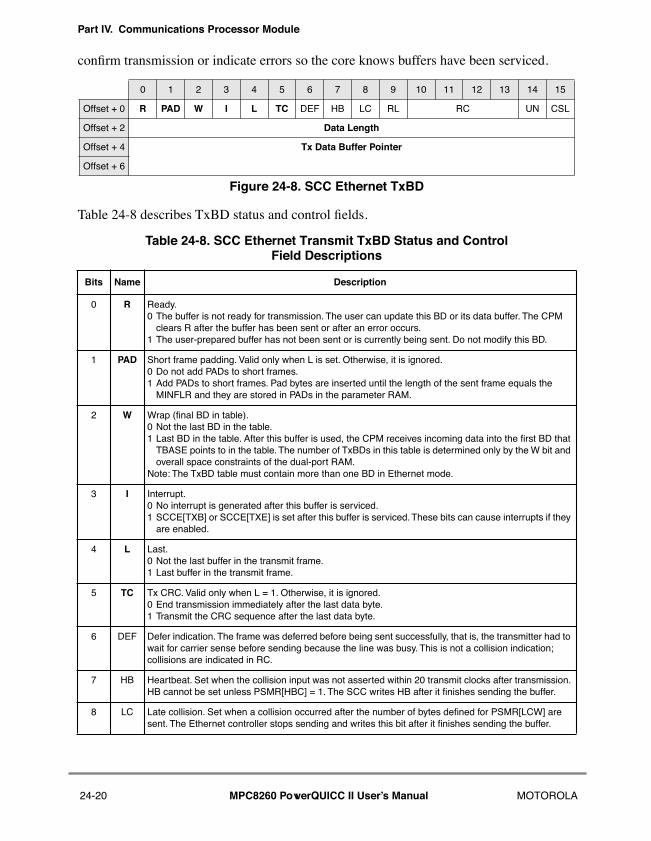
Part IV. Communications Processor Module
conÞrm transmission or indicate errors so the core knows buffers have been serviced.
Table 24-8 describes TxBD status and control Þelds.
0 1 2 3 4 5 6 7 8 9 10 11 12 13 14 15
Offset + 0 R PAD W I L TC DEF HB LC RL RC UN CSL
Offset + 2 Data Length
Offset + 4 Tx Data Buffer Pointer
Offset + 6
Figure 24-8. SCC Ethernet TxBD
Table 24-8. SCC Ethernet Transmit TxBD Status and ControlField Descriptions
Bits Name Description
0 R Ready. 0 The buffer is not ready for transmission. The user can update this BD or its data buffer. The CPM
clears R after the buffer has been sent or after an error occurs.1 The user-prepared buffer has not been sent or is currently being sent. Do not modify this BD.
1 PAD Short frame padding. Valid only when L is set. Otherwise, it is ignored.0 Do not add PADs to short frames.1 Add PADs to short frames. Pad bytes are inserted until the length of the sent frame equals the
MINFLR and they are stored in PADs in the parameter RAM.
2 W Wrap (Þnal BD in table). 0 Not the last BD in the table. 1 Last BD in the table. After this buffer is used, the CPM receives incoming data into the Þrst BD that
TBASE points to in the table. The number of TxBDs in this table is determined only by the W bit and overall space constraints of the dual-port RAM.
Note: The TxBD table must contain more than one BD in Ethernet mode.
3 I Interrupt. 0 No interrupt is generated after this buffer is serviced. 1 SCCE[TXB] or SCCE[TXE] is set after this buffer is serviced. These bits can cause interrupts if they
are enabled.
4 L Last. 0 Not the last buffer in the transmit frame.1 Last buffer in the transmit frame.
5 TC Tx CRC. Valid only when L = 1. Otherwise, it is ignored.0 End transmission immediately after the last data byte. 1 Transmit the CRC sequence after the last data byte.
6 DEF Defer indication. The frame was deferred before being sent successfully, that is, the transmitter had to wait for carrier sense before sending because the line was busy. This is not a collision indication; collisions are indicated in RC.
7 HB Heartbeat. Set when the collision input was not asserted within 20 transmit clocks after transmission. HB cannot be set unless PSMR[HBC] = 1. The SCC writes HB after it Þnishes sending the buffer.
8 LC Late collision. Set when a collision occurred after the number of bytes deÞned for PSMR[LCW] are sent. The Ethernet controller stops sending and writes this bit after it Þnishes sending the buffer.
24-20 MPC8260 PowerQUICC II UserÕs Manual MOTOROLA
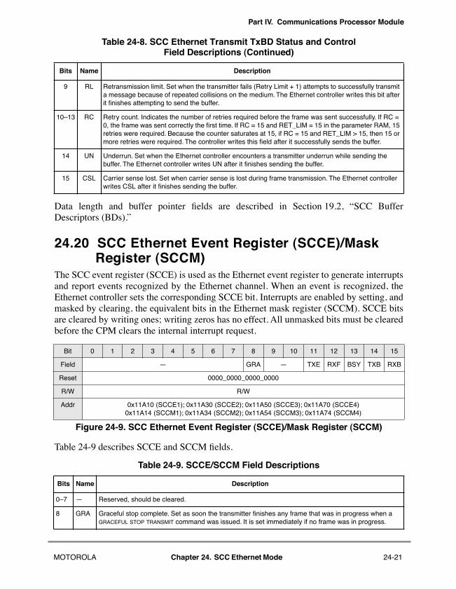
Part IV. Communications Processor Module
Data length and buffer pointer Þelds are described in Section 19.2, ÒSCC BufferDescriptors (BDs).Ó
24.20 SCC Ethernet Event Register (SCCE)/Mask Register (SCCM)
The SCC event register (SCCE) is used as the Ethernet event register to generate interruptsand report events recognized by the Ethernet channel. When an event is recognized, theEthernet controller sets the corresponding SCCE bit. Interrupts are enabled by setting, andmasked by clearing, the equivalent bits in the Ethernet mask register (SCCM). SCCE bitsare cleared by writing ones; writing zeros has no effect. All unmasked bits must be clearedbefore the CPM clears the internal interrupt request.
Table 24-9 describes SCCE and SCCM Þelds.
9 RL Retransmission limit. Set when the transmitter fails (Retry Limit + 1) attempts to successfully transmit a message because of repeated collisions on the medium. The Ethernet controller writes this bit after it Þnishes attempting to send the buffer.
10Ð13 RC Retry count. Indicates the number of retries required before the frame was sent successfully. If RC = 0, the frame was sent correctly the Þrst time. If RC = 15 and RET_LIM = 15 in the parameter RAM, 15 retries were required. Because the counter saturates at 15, if RC = 15 and RET_LIM > 15, then 15 or more retries were required. The controller writes this Þeld after it successfully sends the buffer.
14 UN Underrun. Set when the Ethernet controller encounters a transmitter underrun while sending the buffer. The Ethernet controller writes UN after it Þnishes sending the buffer.
15 CSL Carrier sense lost. Set when carrier sense is lost during frame transmission. The Ethernet controller writes CSL after it Þnishes sending the buffer.
Bit 0 1 2 3 4 5 6 7 8 9 10 11 12 13 14 15
Field Ñ GRA Ñ TXE RXF BSY TXB RXB
Reset 0000_0000_0000_0000
R/W R/W
Addr 0x11A10 (SCCE1); 0x11A30 (SCCE2); 0x11A50 (SCCE3); 0x11A70 (SCCE4)0x11A14 (SCCM1); 0x11A34 (SCCM2); 0x11A54 (SCCM3); 0x11A74 (SCCM4)
Figure 24-9. SCC Ethernet Event Register (SCCE)/Mask Register (SCCM)
Table 24-9. SCCE/SCCM Field Descriptions
Bits Name Description
0Ð7 Ñ Reserved, should be cleared.
8 GRA Graceful stop complete. Set as soon the transmitter Þnishes any frame that was in progress when a GRACEFUL STOP TRANSMIT command was issued. It is set immediately if no frame was in progress.
Table 24-8. SCC Ethernet Transmit TxBD Status and ControlField Descriptions (Continued)
Bits Name Description
MOTOROLA Chapter 24. SCC Ethernet Mode 24-21
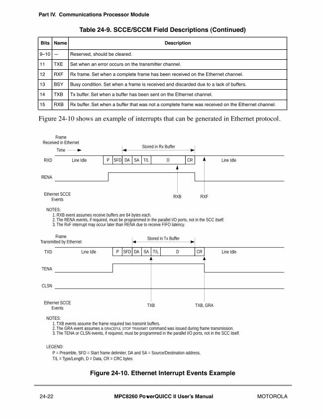
Part IV. Communications Processor Module
Figure 24-10 shows an example of interrupts that can be generated in Ethernet protocol.
Figure 24-10. Ethernet Interrupt Events Example
9Ð10 Ñ Reserved, should be cleared.
11 TXE Set when an error occurs on the transmitter channel.
12 RXF Rx frame. Set when a complete frame has been received on the Ethernet channel.
13 BSY Busy condition. Set when a frame is received and discarded due to a lack of buffers.
14 TXB Tx buffer. Set when a buffer has been sent on the Ethernet channel.
15 RXB Rx buffer. Set when a buffer that was not a complete frame was received on the Ethernet channel.
Table 24-9. SCCE/SCCM Field Descriptions (Continued)
Bits Name Description
RXB
Line Idle
Stored in Rx Buffer
RXD
RENA
FrameReceived in Ethernet
Time
Line Idle
TXD
TENA
FrameTransmitted by Ethernet
CLSN
TXB, GRATXB
Line Idle Line Idle
Stored in Tx Buffer
NOTES:
Ethernet SCCEEvents
1. RXB event assumes receive buffers are 64 bytes each.2. The RENA events, if required, must be programmed in the parallel I/O ports, not in the SCC itself.3. The RxF interrupt may occur later than RENA due to receive FIFO latency.
NOTES:
Ethernet SCCEEvents
1. TXB events assume the frame required two transmit buffers.2. The GRA event assumes a GRACEFUL STOP TRANSMIT command was issued during frame transmission.
P SFD DA SA CR
RXF
3. The TENA or CLSN events, if required, must be programmed in the parallel I/O ports, not in the SCC itself.
T/L D
P SFD DA SA CRT/L D
LEGEND:P = Preamble, SFD = Start frame delimiter, DA and SA = Source/Destination address,T/L = Type/Length, D = Data, CR = CRC bytes
24-22 MPC8260 PowerQUICC II UserÕs Manual MOTOROLA
Part IV. Communications Processor Module
Note that the SCC status register (SCCS) cannot be used with the Ethernet protocol. Thecurrent state of the RENA and CLSN signals can be found in the parallel I/O ports.
24.21 SCC Ethernet Programming ExampleThe following is an initialization sequence for the SCC2 in Ethernet mode. The CLK3 pinis used for the Ethernet receiver and CLK4 is used for the transmitter.
1. ConÞgure port D pins to enable TXD2 and RXD2. Set PPARD[27,28] and PDIRD[27] and clear PDIRD[28] and PSORD[27,28].
2. ConÞgure ports C and D pins to enable TENA2 (RTS2), CLSN2 (CTS2) and RENA2 (CD2). Set PPARD[26], PPARC[12,13] and PDIRD[26] and clear PDIRC[12,13], PSORC[12,13] and PSORD[26].
3. ConÞgure port C pins to enable CLK3 and CLK4. Set PPARC[28,29] and clear PDIRC[28,29] and PSORC[28,29].
4. Connect CLK3 to the SCC2 receiver and CLK4 to the transmitter using the CPM mux. Program CMXSCR[R2CS] to 0b110 and CMXSCR[T2CS] to 0b111.
5. Connect the SCC2 to the NMSI and clear CMXSCR[SC2].
6. Write RBASE and TBASE in the SCC2 parameter RAM to point to the RxBD and TxBD in the dual-port RAM. Assuming one RxBD at the beginning of the dual-port RAM and one TxBD following that RxBD, write RBASE with 0x0000 and TBASE with 0x0008.
7. Write 0x04A1_0000 to the CPCR to execute an INIT RX AND TX PARAMETERS command for this channel.
8. Clear CRCEC, ALEC, and DISFC for clarity.
9. Write PAD with 0x8888 for the PAD value.
10. Write RET_LIM with 0x000F.
11. Write MFLR with 0x05EE to make the maximum frame size 1518 bytes.
12. Write MINFLR with 0x0040 to make the minimum frame size 64 bytes.
13. Write MAXD1 and MAXD2 with 0x05F0 to make the maximum DMA count 1520 bytes.
14. Clear GADDR1ÐGADDR4. The group hash table is not used.
15. Write PADDR1_H with 0x0000, PADDR1_M with 0x0000, and PADDR1_L with 0x0040 to conÞgure the physical address.
16. Clear P_PER. It is not used.
17. Clear IADDR1ÐIADDR4. The individual hash table is not used.
18. Clear TADDR_H, TADDR_M, and TADDR_L for clarity.
19. Initialize the RxBD and assume the Rx data buffer is at 0x0000_1000 in main memory. Write 0xB000 to RxBD[Status and Control], 0x0000 to RxBD[Data Length] (optional), and 0x0000_1000 to RxBD[Buffer Pointer].
MOTOROLA Chapter 24. SCC Ethernet Mode 24-23
Part IV. Communications Processor Module
20. Initialize the TxBD and assume the Tx data frame is at 0x0000_2000 in main memory and contains fourteen 8-bit characters (destination and source addresses plus the type Þeld). Write 0xFC00 to TxBD[Status and Control], add PAD to the frame and generate a CRC. Then write 0x000D to TxBD[Data Length] and 0x0000_2000 to TxBD[Buffer Pointer].
21. Write 0xFFFF to the SCCE register to clear any previous events.
22. Write 0x001A to the SCCM register to enable the TXE, RXF, and TXB interrupts.
23. Write 0x0040_0000 to the SIU interrupt mask register low (SIMR_L) so the SMC1 can generate a system interrupt. Initialize SIU interrupt pending register low (SIPNR_L) by writing 0xFFFF_FFFF to it.
24. Write 0x0000_0000 to GSMR_H2 to enable normal operation of all modes.
25. Write 0x1088_000C to the GSMR_L2 register to conÞgure CTS (CLSN) and CD (RENA) to automatically control transmission and reception (DIAG bits) and the Ethernet mode. TCI is set to allow more setup time for the EEST to receive the MPC8260 transmit data. TPL and TPP are set for Ethernet requirements. The DPLL is not used with Ethernet. Note that the ENT and ENR are not enabled yet.
26. Write 0xD555 to the DSR.
27. Set the PSMR2 to 0x0A0A to conÞgure 32-bit CRC, promiscuous mode, and begin searching for the start frame delimiter 22 bits after RENA2 (CD2).
28. Write 0x1088_003C to GSMR_L2 to enable the SCC2 transmitter and receiver. This additional write ensures that ENT and ENR are enabled last.
After 14 bytes and the 46 bytes of automatic pad (plus the 4 bytes of CRC) are sent, theTxBD is closed. Additionally, the receive buffer is closed after a frame is received. Any datareceived after 1520 bytes or a single frame causes a busy (out-of-buffers) condition becauseonly one RxBD is prepared.
24-24 MPC8260 PowerQUICC II UserÕs Manual MOTOROLA
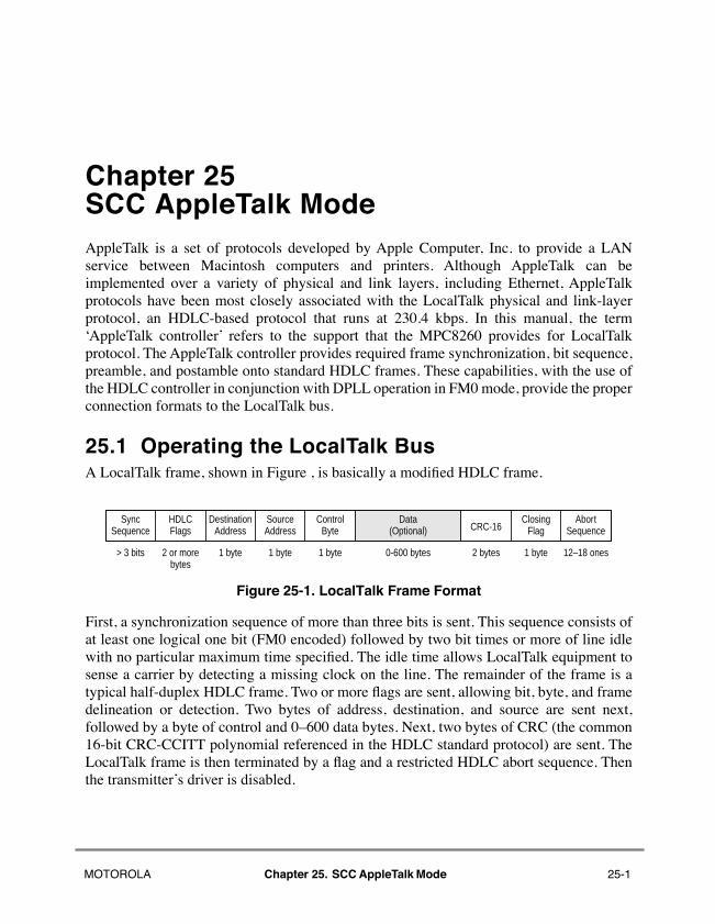
Chapter 25 SCC AppleTalk Mode250250
AppleTalk is a set of protocols developed by Apple Computer, Inc. to provide a LANservice between Macintosh computers and printers. Although AppleTalk can beimplemented over a variety of physical and link layers, including Ethernet, AppleTalkprotocols have been most closely associated with the LocalTalk physical and link-layerprotocol, an HDLC-based protocol that runs at 230.4 kbps. In this manual, the termÔAppleTalk controllerÕ refers to the support that the MPC8260 provides for LocalTalkprotocol. The AppleTalk controller provides required frame synchronization, bit sequence,preamble, and postamble onto standard HDLC frames. These capabilities, with the use ofthe HDLC controller in conjunction with DPLL operation in FM0 mode, provide the properconnection formats to the LocalTalk bus.
25.1 Operating the LocalTalk BusA LocalTalk frame, shown in Figure , is basically a modiÞed HDLC frame.
Figure 25-1. LocalTalk Frame Format
First, a synchronization sequence of more than three bits is sent. This sequence consists ofat least one logical one bit (FM0 encoded) followed by two bit times or more of line idlewith no particular maximum time speciÞed. The idle time allows LocalTalk equipment tosense a carrier by detecting a missing clock on the line. The remainder of the frame is atypical half-duplex HDLC frame. Two or more ßags are sent, allowing bit, byte, and framedelineation or detection. Two bytes of address, destination, and source are sent next,followed by a byte of control and 0Ð600 data bytes. Next, two bytes of CRC (the common16-bit CRC-CCITT polynomial referenced in the HDLC standard protocol) are sent. TheLocalTalk frame is then terminated by a ßag and a restricted HDLC abort sequence. Thenthe transmitterÕs driver is disabled.
> 3 bits 2 or more 1 byte 1 byte 0-600 bytes 2 bytes 12–18 ones1 byte 1 bytebytes
HDLCCRC-16Flags
DestinationAddress
Data(Optional)
ControlByte
SyncSequence
SourceAddress
ClosingFlag
AbortSequence
MOTOROLA Chapter 25. SCC AppleTalk Mode 25-1
Part IV. Communications Processor Module
The control byte within the LocalTalk frame indicates the type of frame. Control bytevalues from 0x01Ð0x7F are data frames; control byte values from 0x80Ð0xFF are controlframes. Four control frames are deÞned:
¥ ENQÑEnquiry¥ ACKÑEnquiry acknowledgment¥ RTSÑRequest to send a data frame¥ CTSÑClear to send a data frame
Frames are sent in groups known as dialogs, which are handled by the software. Forinstance, to transfer a data frame, three frames are sent over the network. An RTS frame(not to be confused with the RS-232 RTS pin) is sent to request the network, a CTS frameis sent by the destination node, and the data frame is sent by the requesting node. Thesethree frames comprise one possible type of dialog. After a dialog begins, other nodes cannotstart sending until the dialog is complete. Frames within a dialog are sent with a maximuminterframe gap (IFG) of 200 µs. Although the LocalTalk speciÞcation does not state it, thereis also a minimum recommended IFG of 50 µs. Dialogs must be separated by a minimuminterdialog gap (IDG) of 400 µs. In general, these gaps are implemented by the software.
Depending on the protocol, collisions should be encountered only during RTS and ENQframes. Once frame transmission begins, it is fully sent, regardless of whether it collideswith another frame. ENQ frames are infrequent and are sent only when a node powers upand enters the network. A higher-level protocol controls the uniqueness and transmissionof ENQ frames.
In addition to the frame Þelds, LocalTalk requires that the frame be FM0 (differentialManchester space) encoded, which requires one level transition on every bit boundary. Ifthe value to be encoded is a logical zero, FM0 requires a second transition in the middle ofthe bit time. The purpose of FM0 encoding is to avoid having to transmit clockinginformation on a separate wire. With FM0, the clocking information is present whenevervalid data is present.
25.2 FeaturesThe following list summarizes the features of the SCC in AppleTalk mode:
¥ Superset of the HDLC controller features
¥ FM0 encoding/decoding
¥ Programmable transmission of sync sequence
¥ Automatic postamble transmission
¥ Reception of sync sequence does not cause extra SCCE[DCC] interrupts
¥ Reception is automatically disabled while sending a frame
¥ Transmit-on-demand feature expedites frames
¥ Connects directly to an RS-422 transceiver
25-2 MPC8260 PowerQUICC II UserÕs Manual MOTOROLA
Part IV. Communications Processor Module
25.3 Connecting to AppleTalkAs shown in Figure , the MPC8260 connects to LocalTalk, and, using TXD, RTS, andRXD, is an interface for the RS-422 transceiver. The RS-422, in turn, is an interface for theLocalTalk connector. Although it is not shown, a passive RC circuit is recommendedbetween the transceiver and connector.
Figure 25-2. Connecting the MPC8260 to LocalTalk
The 16´ overspeed of a 3.686-MHz clock can be generated from an external frequencysource or from one of the baud rate generators if the resulting output frequency is close toa multiple of the 3.686 MHz frequency. The MPC8260 asserts RTS throughout the durationof the frame so that RTS can be used to enable the RS-422 transmit driver.
25.4 Programming the SCC in AppleTalk ModeThe AppleTalk controller is implemented by setting certain bits in the HDLC controller.Otherwise, Chapter 21, ÒSCC HDLC Mode,Ó describes how to program the HDLCcontroller. Use GSMR, PSMR, or TODR to program the AppleTalk controller.
25.4.1 Programming the GSMRProgram the GSMR as described below:
1. Set MODE to 0b0010 (AppleTalk).
2. Set DIAG to 0b00 for normal operation, with CD and CTS grounded or conÞgured for parallel I/O. This causes CD and CTS to be internally asserted to the SCC.
3. Set RDCR and TDCR to (0b10) a 16´ clock.
4. Set the TENC and RENC bits to 0b010 (FM0).
Two HDLCCRC-16Flags
DestinationAddress Data
ControlByte
6-Bit SyncSequence
SourceAddress
ClosingFlag
16 Ones(Abort)
RS-422
TXD
RTS
RXD
Stored in Receive Buffer
Standard HDLC frame handling
MINI-DIN 8
Stored in Transmit Buffer
SCC
RTS
TXD
Tx Data
Tx Enable
Rx Data
MPC8260
Connection
MOTOROLA Chapter 25. SCC AppleTalk Mode 25-3
Part IV. Communications Processor Module
5. Clear TEND for default operation.
6. Set TPP to 0b11 for a preamble pattern of all ones.
7. Set TPL to 0b000 to transmit the next frame with no synchronization sequence and to 001 to transmit the next frame with the LocalTalk synchronization sequence. For example, data frames do not require a preceding synchronization sequence. These bits may be modiÞed on-the-ßy if the AppleTalk protocol is selected.
8. Clear TINV and RINV so data will not be inverted.
9. Set TSNC to 1.5 bit times (0b10).
10. Clear EDGE. Both the positive and negative edges are used to change the sample point (default).
11. Clear RTSM (default).
12. Set all other bits to zero or default.
13. Set ENT and ENR as the last step to begin operation.
25.4.2 Programming the PSMR Follow these steps to program the protocol-speciÞc mode register:
1. Set NOF to 0b0001 giving two ßags before frames (one opening ßag, plus one additional ßag).
2. Set CRC 16-bit CRC-CCITT.
3. Set DRT.
4. Set all other bits to zero or default.
For the PSMR deÞnition, see Section 21.8, ÒHDLC Mode Register (PSMR).Ó
25.4.3 Programming the TODRUse the transmit-on-demand (TODR) register to expedite a transmit frame. SeeSection 19.1.4, ÒTransmit-on-Demand Register (TODR).Ó
25.4.4 SCC AppleTalk Programming ExampleExcept for the previously discussed register programming, use the example inSection 21.14.6, ÒHDLC Bus Protocol Programming.Ó
25-4 MPC8260 PowerQUICC II UserÕs Manual MOTOROLA
Chapter 26 Serial Management Controllers (SMCs)260260
The two serial management controllers (SMCs) are full-duplex ports that can be conÞguredindependently to support one of three protocols or modesÑUART, transparent, or general-circuit interface (GCI). Simple UART operation is used to provide a debug/monitor port inan application, which allows the SCCs to be free for other purposes. The SMC in UARTmode is not as complex as that of the SCC in UART mode. The SMC clock can be derivedfrom one of the internal baud rate generators or from an external clock signal. However, theclock should be a 16´ clock.
In totally transparent mode, the SMC can be connected to a TDM channel (such as a T1line) or directly to its own set of signals. The receive and transmit clocks are derived fromthe TDM channel, the internal baud rate generators, or from an external 1´ clock. Thetransparent protocol allows the transmitter and receiver to use the external synchronizationsignal. The SMC in transparent mode is not as complex as that of the SCC in transparentmode.
Each SMC supports the C/I and monitor channels of the GCI bus, for which the SMCconnects to a time-division multiplex (TDM) channel in a serial interface (SIx). SMCssupport loopback and echo modes for testing. The SMC receiver and transmitter aredouble-buffered, corresponding to an effective FIFO size (latency) of two characters.Chapter 14, ÒSerial Interface with Time-Slot Assigner,Ó describes GCI interfaceconÞguration.
MOTOROLA Chapter 26. Serial Management Controllers (SMCs) 26-1
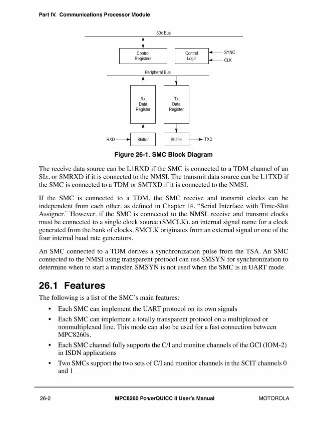
Part IV. Communications Processor Module
Figure 26-1. SMC Block Diagram
The receive data source can be L1RXD if the SMC is connected to a TDM channel of anSIx, or SMRXD if it is connected to the NMSI. The transmit data source can be L1TXD ifthe SMC is connected to a TDM or SMTXD if it is connected to the NMSI.
If the SMC is connected to a TDM, the SMC receive and transmit clocks can beindependent from each other, as deÞned in Chapter 14, ÒSerial Interface with Time-SlotAssigner.Ó However, if the SMC is connected to the NMSI, receive and transmit clocksmust be connected to a single clock source (SMCLK), an internal signal name for a clockgenerated from the bank of clocks. SMCLK originates from an external signal or one of thefour internal baud rate generators.
An SMC connected to a TDM derives a synchronization pulse from the TSA. An SMCconnected to the NMSI using transparent protocol can use SMSYN for synchronization todetermine when to start a transfer. SMSYN is not used when the SMC is in UART mode.
26.1 FeaturesThe following is a list of the SMCÕs main features:
¥ Each SMC can implement the UART protocol on its own signals
¥ Each SMC can implement a totally transparent protocol on a multiplexed or nonmultiplexed line. This mode can also be used for a fast connection between MPC8260s.
¥ Each SMC channel fully supports the C/I and monitor channels of the GCI (IOM-2) in ISDN applications
¥ Two SMCs support the two sets of C/I and monitor channels in the SCIT channels 0 and 1
Shifter
SYNC
RxData
Register
TxData
Register
RXD
ControlLogic
TXD
ControlRegisters
Shifter
Peripheral Bus
CLK
60x Bus
26-2 MPC8260 PowerQUICC II UserÕs Manual MOTOROLA
Part IV. Communications Processor Module
¥ Full-duplex operation
¥ Local loopback and echo capability for testing
26.2 Common SMC Settings and ConÞgurationsThe following sections describe settings and conÞgurations that are common to the SMCs.
26.2.1 SMC Mode Registers (SMCMR1/SMCMR2)The SMC mode registers (SMCMR1 and SMCMR2), shown in Figure 26-2, selects theSMC mode as well as mode-speciÞc parameters. The functions of SMCMR[8Ð15] are thesame for each protocol. Bits 0Ð7 vary according to protocol selected by the SM bits.
Bit 0 1 2 3 4 5 6 7 8 9 10 11 12 13 14 15
Field: UART Ñ CLEN SL PEN PM Ñ SM DM TEN REN
Transparent Ñ BS REVD
GCI ME Ñ C#
Reset 0000_0000_0000_0000
R/W R/W
Address 0x11A82 (SMCMR1), 0x11A92 (SMCMR2)
Figure 26-2. SMC Mode Registers (SMCMR1/SMCMR2)
MOTOROLA Chapter 26. Serial Management Controllers (SMCs) 26-3
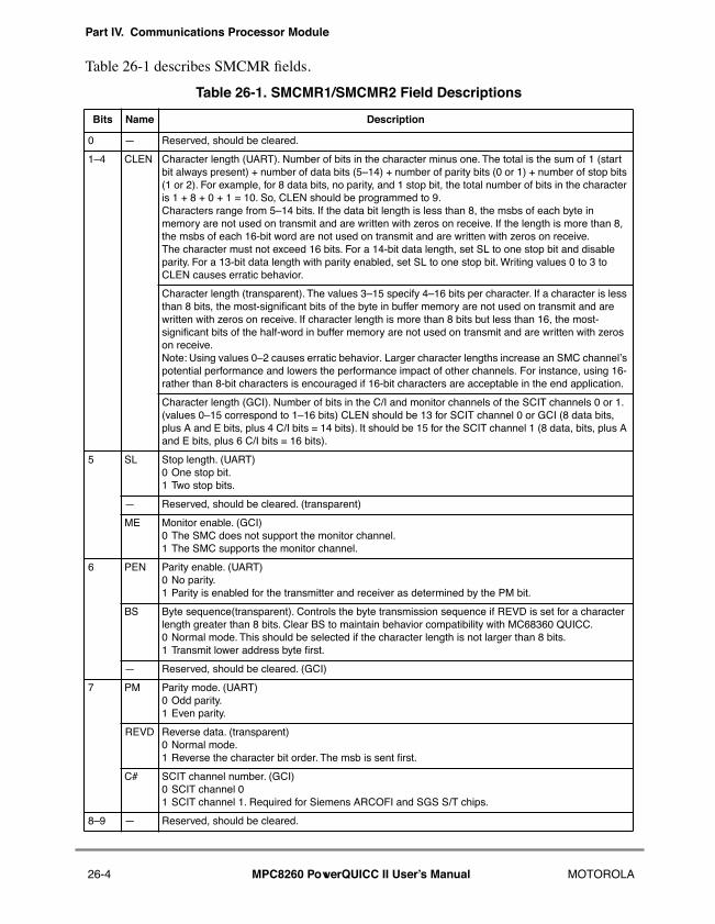
Part IV. Communications Processor Module
Table 26-1 describes SMCMR Þelds.
Table 26-1. SMCMR1/SMCMR2 Field Descriptions
Bits Name Description
0 Ñ Reserved, should be cleared.
1Ð4 CLEN Character length (UART). Number of bits in the character minus one. The total is the sum of 1 (start bit always present) + number of data bits (5Ð14) + number of parity bits (0 or 1) + number of stop bits (1 or 2). For example, for 8 data bits, no parity, and 1 stop bit, the total number of bits in the character is 1 + 8 + 0 + 1 = 10. So, CLEN should be programmed to 9.Characters range from 5Ð14 bits. If the data bit length is less than 8, the msbs of each byte in memory are not used on transmit and are written with zeros on receive. If the length is more than 8, the msbs of each 16-bit word are not used on transmit and are written with zeros on receive.The character must not exceed 16 bits. For a 14-bit data length, set SL to one stop bit and disable parity. For a 13-bit data length with parity enabled, set SL to one stop bit. Writing values 0 to 3 to CLEN causes erratic behavior.
Character length (transparent). The values 3Ð15 specify 4Ð16 bits per character. If a character is less than 8 bits, the most-signiÞcant bits of the byte in buffer memory are not used on transmit and are written with zeros on receive. If character length is more than 8 bits but less than 16, the most-signiÞcant bits of the half-word in buffer memory are not used on transmit and are written with zeros on receive.Note: Using values 0Ð2 causes erratic behavior. Larger character lengths increase an SMC channelÕs potential performance and lowers the performance impact of other channels. For instance, using 16- rather than 8-bit characters is encouraged if 16-bit characters are acceptable in the end application.
Character length (GCI). Number of bits in the C/I and monitor channels of the SCIT channels 0 or 1. (values 0Ð15 correspond to 1Ð16 bits) CLEN should be 13 for SCIT channel 0 or GCI (8 data bits, plus A and E bits, plus 4 C/I bits = 14 bits). It should be 15 for the SCIT channel 1 (8 data, bits, plus A and E bits, plus 6 C/I bits = 16 bits).
5 SL Stop length. (UART)0 One stop bit.1 Two stop bits.
Ñ Reserved, should be cleared. (transparent)
ME Monitor enable. (GCI)0 The SMC does not support the monitor channel.1 The SMC supports the monitor channel.
6 PEN Parity enable. (UART)0 No parity.1 Parity is enabled for the transmitter and receiver as determined by the PM bit.
BS Byte sequence(transparent). Controls the byte transmission sequence if REVD is set for a character length greater than 8 bits. Clear BS to maintain behavior compatibility with MC68360 QUICC.0 Normal mode. This should be selected if the character length is not larger than 8 bits.1 Transmit lower address byte Þrst.
Ñ Reserved, should be cleared. (GCI)
7 PM Parity mode. (UART)0 Odd parity.1 Even parity.
REVD Reverse data. (transparent)0 Normal mode.1 Reverse the character bit order. The msb is sent Þrst.
C# SCIT channel number. (GCI)0 SCIT channel 01 SCIT channel 1. Required for Siemens ARCOFI and SGS S/T chips.
8Ð9 Ñ Reserved, should be cleared.
26-4 MPC8260 PowerQUICC II UserÕs Manual MOTOROLA
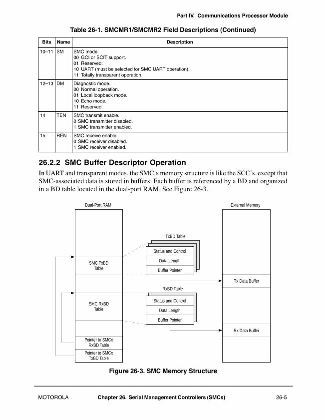
Part IV. Communications Processor Module
26.2.2 SMC Buffer Descriptor OperationIn UART and transparent modes, the SMCÕs memory structure is like the SCCÕs, except thatSMC-associated data is stored in buffers. Each buffer is referenced by a BD and organizedin a BD table located in the dual-port RAM. See Figure 26-3.
Figure 26-3. SMC Memory Structure
10Ð11 SM SMC mode. 00 GCI or SCIT support.01 Reserved.10 UART (must be selected for SMC UART operation).11 Totally transparent operation.
12Ð13 DM Diagnostic mode. 00 Normal operation.01 Local loopback mode.10 Echo mode.11 Reserved.
14 TEN SMC transmit enable. 0 SMC transmitter disabled.1 SMC transmitter enabled.
15 REN SMC receive enable. 0 SMC receiver disabled.1 SMC receiver enabled.
Table 26-1. SMCMR1/SMCMR2 Field Descriptions (Continued)
Bits Name Description
Status and Control
Data Length
Buffer Pointer
Pointer to SMCxTxBD Table
Pointer to SMCxRxBD Table
SMC RxBDTable
SMC TxBDTable
Dual-Port RAM
Status and Control
Data Length
Buffer Pointer
Tx Data Buffer
External Memory
RxBD Table
TxBD Table
Rx Data Buffer
MOTOROLA Chapter 26. Serial Management Controllers (SMCs) 26-5
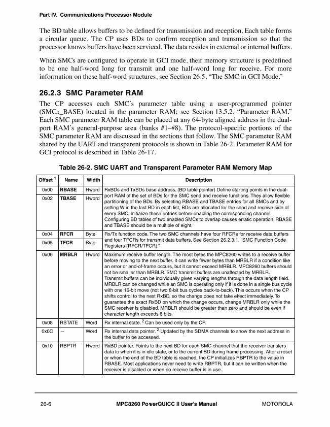
Part IV. Communications Processor Module
The BD table allows buffers to be deÞned for transmission and reception. Each table formsa circular queue. The CP uses BDs to conÞrm reception and transmission so that theprocessor knows buffers have been serviced. The data resides in external or internal buffers.
When SMCs are conÞgured to operate in GCI mode, their memory structure is predeÞnedto be one half-word long for transmit and one half-word long for receive. For moreinformation on these half-word structures, see Section 26.5, ÒThe SMC in GCI Mode.Ó
26.2.3 SMC Parameter RAMThe CP accesses each SMCÕs parameter table using a user-programmed pointer(SMCx_BASE) located in the parameter RAM; see Section 13.5.2, ÒParameter RAM.ÓEach SMC parameter RAM table can be placed at any 64-byte aligned address in the dual-port RAMÕs general-purpose area (banks #1Ð#8). The protocol-speciÞc portions of theSMC parameter RAM are discussed in the sections that follow. The SMC parameter RAMshared by the UART and transparent protocols is shown in Table 26-2. Parameter RAM forGCI protocol is described in Table 26-17.
Table 26-2. SMC UART and Transparent Parameter RAM Memory Map
Offset 1 Name Width Description
0x00 RBASE Hword RxBDs and TxBDs base address. (BD table pointer) DeÞne starting points in the dual-port RAM of the set of BDs for the SMC send and receive functions. They allow ßexible partitioning of the BDs. By selecting RBASE and TBASE entries for all SMCs and by setting W in the last BD in each list, BDs are allocated for the send and receive side of every SMC. Initialize these entries before enabling the corresponding channel. ConÞguring BD tables of two enabled SMCs to overlap causes erratic operation. RBASE and TBASE should be a multiple of eight.
0x02 TBASE Hword
0x04 RFCR Byte Rx/Tx function code. The two SMC channels have four RFCRs for receive data buffers and four TFCRs for transmit data buffers. See Section 26.2.3.1, ÒSMC Function Code Registers (RFCR/TFCR).Ó
0x05 TFCR Byte
0x06 MRBLR Hword Maximum receive buffer length. The most bytes the MPC8260 writes to a receive buffer before moving to the next buffer. It can write fewer bytes than MRBLR if a condition like an error or end-of-frame occurs, but it cannot exceed MRBLR. MPC8260 buffers should not be smaller than MRBLR. SMC transmit buffers are unaffected by MRBLR. Transmit buffers can be individually given varying lengths through the data length Þeld. MRBLR can be changed while an SMC is operating only if it is done in a single bus cycle with one 16-bit move (not two 8-bit bus cycles back-to-back). This occurs when the CP shifts control to the next RxBD, so the change does not take effect immediately. To guarantee the exact RxBD on which the change occurs, change MRBLR only while the SMC receiver is disabled. MRBLR should be greater than zero and should be even if character length exceeds 8 bits.
0x08 RSTATE Word Rx internal state. 2 Can be used only by the CP.
0x0C Ñ Word Rx internal data pointer. 2 Updated by the SDMA channels to show the next address in the buffer to be accessed.
0x10 RBPTR Hword RxBD pointer. Points to the next BD for each SMC channel that the receiver transfers data to when it is in idle state, or to the current BD during frame processing. After a reset or when the end of the BD table is reached, the CP initializes RBPTR to the value in RBASE. Most applications never need to write RBPTR, but it can be written when the receiver is disabled or when no receive buffer is in use.
26-6 MPC8260 PowerQUICC II UserÕs Manual MOTOROLA
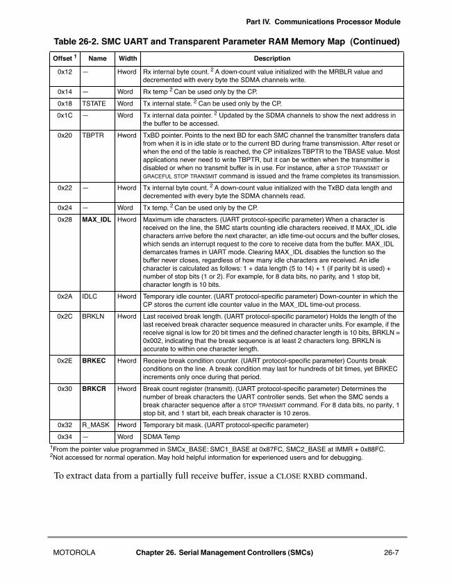
Part IV. Communications Processor Module
To extract data from a partially full receive buffer, issue a CLOSE RXBD command.
0x12 Ñ Hword Rx internal byte count. 2 A down-count value initialized with the MRBLR value and decremented with every byte the SDMA channels write.
0x14 Ñ Word Rx temp 2 Can be used only by the CP.
0x18 TSTATE Word Tx internal state. 2 Can be used only by the CP.
0x1C Ñ Word Tx internal data pointer. 2 Updated by the SDMA channels to show the next address in the buffer to be accessed.
0x20 TBPTR Hword TxBD pointer. Points to the next BD for each SMC channel the transmitter transfers data from when it is in idle state or to the current BD during frame transmission. After reset or when the end of the table is reached, the CP initializes TBPTR to the TBASE value. Most applications never need to write TBPTR, but it can be written when the transmitter is disabled or when no transmit buffer is in use. For instance, after a STOP TRANSMIT or GRACEFUL STOP TRANSMIT command is issued and the frame completes its transmission.
0x22 Ñ Hword Tx internal byte count. 2 A down-count value initialized with the TxBD data length and decremented with every byte the SDMA channels read.
0x24 Ñ Word Tx temp. 2 Can be used only by the CP.
0x28 MAX_IDL Hword Maximum idle characters. (UART protocol-speciÞc parameter) When a character is received on the line, the SMC starts counting idle characters received. If MAX_IDL idle characters arrive before the next character, an idle time-out occurs and the buffer closes, which sends an interrupt request to the core to receive data from the buffer. MAX_IDL demarcates frames in UART mode. Clearing MAX_IDL disables the function so the buffer never closes, regardless of how many idle characters are received. An idle character is calculated as follows: 1 + data length (5 to 14) + 1 (if parity bit is used) + number of stop bits (1 or 2). For example, for 8 data bits, no parity, and 1 stop bit, character length is 10 bits.
0x2A IDLC Hword Temporary idle counter. (UART protocol-speciÞc parameter) Down-counter in which the CP stores the current idle counter value in the MAX_IDL time-out process.
0x2C BRKLN Hword Last received break length. (UART protocol-speciÞc parameter) Holds the length of the last received break character sequence measured in character units. For example, if the receive signal is low for 20 bit times and the deÞned character length is 10 bits, BRKLN = 0x002, indicating that the break sequence is at least 2 characters long. BRKLN is accurate to within one character length.
0x2E BRKEC Hword Receive break condition counter. (UART protocol-speciÞc parameter) Counts break conditions on the line. A break condition may last for hundreds of bit times, yet BRKEC increments only once during that period.
0x30 BRKCR Hword Break count register (transmit). (UART protocol-speciÞc parameter) Determines the number of break characters the UART controller sends. Set when the SMC sends a break character sequence after a STOP TRANSMIT command. For 8 data bits, no parity, 1 stop bit, and 1 start bit, each break character is 10 zeros.
0x32 R_MASK Hword Temporary bit mask. (UART protocol-speciÞc parameter)
0x34 Ñ Word SDMA Temp
1From the pointer value programmed in SMCx_BASE: SMC1_BASE at 0x87FC, SMC2_BASE at IMMR + 0x88FC.2Not accessed for normal operation. May hold helpful information for experienced users and for debugging.
Table 26-2. SMC UART and Transparent Parameter RAM Memory Map (Continued)
Offset 1 Name Width Description
MOTOROLA Chapter 26. Serial Management Controllers (SMCs) 26-7
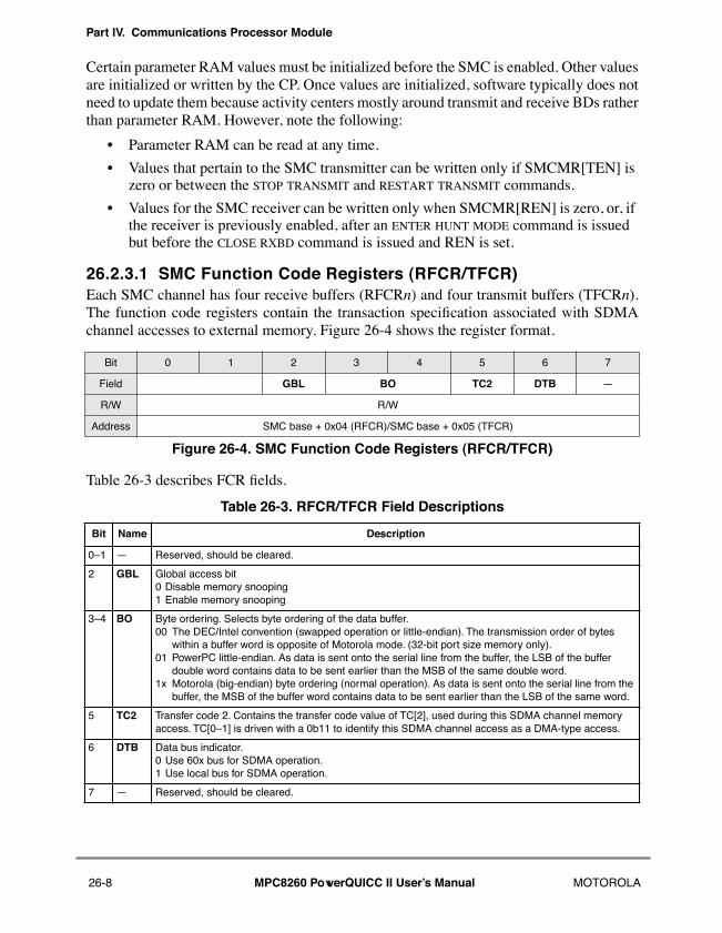
Part IV. Communications Processor Module
Certain parameter RAM values must be initialized before the SMC is enabled. Other valuesare initialized or written by the CP. Once values are initialized, software typically does notneed to update them because activity centers mostly around transmit and receive BDs ratherthan parameter RAM. However, note the following:
¥ Parameter RAM can be read at any time.
¥ Values that pertain to the SMC transmitter can be written only if SMCMR[TEN] is zero or between the STOP TRANSMIT and RESTART TRANSMIT commands.
¥ Values for the SMC receiver can be written only when SMCMR[REN] is zero, or, if the receiver is previously enabled, after an ENTER HUNT MODE command is issued but before the CLOSE RXBD command is issued and REN is set.
26.2.3.1 SMC Function Code Registers (RFCR/TFCR)Each SMC channel has four receive buffers (RFCRn) and four transmit buffers (TFCRn).The function code registers contain the transaction speciÞcation associated with SDMAchannel accesses to external memory. Figure 26-4 shows the register format.
Table 26-3 describes FCR Þelds.
Bit 0 1 2 3 4 5 6 7
Field GBL BO TC2 DTB Ñ
R/W R/W
Address SMC base + 0x04 (RFCR)/SMC base + 0x05 (TFCR)
Figure 26-4. SMC Function Code Registers (RFCR/TFCR)
Table 26-3. RFCR/TFCR Field Descriptions
Bit Name Description
0Ð1 Ñ Reserved, should be cleared.
2 GBL Global access bit0 Disable memory snooping1 Enable memory snooping
3Ð4 BO Byte ordering. Selects byte ordering of the data buffer. 00 The DEC/Intel convention (swapped operation or little-endian). The transmission order of bytes
within a buffer word is opposite of Motorola mode. (32-bit port size memory only).01 PowerPC little-endian. As data is sent onto the serial line from the buffer, the LSB of the buffer
double word contains data to be sent earlier than the MSB of the same double word. 1x Motorola (big-endian) byte ordering (normal operation). As data is sent onto the serial line from the
buffer, the MSB of the buffer word contains data to be sent earlier than the LSB of the same word.
5 TC2 Transfer code 2. Contains the transfer code value of TC[2], used during this SDMA channel memory access. TC[0Ð1] is driven with a 0b11 to identify this SDMA channel access as a DMA-type access.
6 DTB Data bus indicator.0 Use 60x bus for SDMA operation.1 Use local bus for SDMA operation.
7 Ñ Reserved, should be cleared.
26-8 MPC8260 PowerQUICC II UserÕs Manual MOTOROLA
Part IV. Communications Processor Module
26.2.4 Disabling SMCs On-the-FlyAn SMC can be disabled and reenabled later by ensuring that buffers are closed properlyand new data is transferred to or from a new buffer. Such a sequence is required if theparameters to be changed are not dynamic. If the register or bit description states thatdynamic changes are allowed, the sequences need not be followed and the register or bitsmay be changed immediately.
Note that the SMC does not have to be fully disabled for parameter RAM to be modiÞed.Table 26-2 describes when parameter RAM values can be modiÞed. To disable all SCCs,SMCs, the SPI, and the I2C, use the CPCR to reset the CPM with a single command.
26.2.4.1 SMC Transmitter Full SequenceFollow these steps to fully enable or disable the SMC transmitter:
1. If the SMC is sending data, issue a STOP TRANSMIT command to stop transmission smoothly. If the SMC is not sending, if TBPTR is overwritten, or if an INIT TX PARAMETERS command is executed, this command is not required.
2. Clear SMCMR[TEN] to disable the SMC transmitter and put it in reset state.
3. Update SMC transmit parameters, including the parameter RAM. To switch protocols or reinitialize parameters, issue an INIT TX PARAMETERS command.
4. Issue a RESTART TRANSMIT if an INIT TX PARAMETERS was issued in step 3.
5. Set SMCMR[TEN]. Transmission now begins using the TxBD that the TBPTR value pointed to as soon as the R bit is set in the TxBD.
26.2.4.2 SMC Transmitter Shortcut SequenceThis shorter sequence reinitializes transmit parameters to the state they had after reset.
1. Clear SMCMR[TEN].2. Issue an INIT TX PARAMETERS command and make any additional changes.3. Set SMCMR[TEN].
26.2.4.3 SMC Receiver Full SequenceFollow these steps to fully enable or disable the receiver:
1. Clear SMCMR[REN]. Reception is aborted immediately, which disables the SMC receiver and puts it in a reset state.
2. Modify SMC receive parameters, including parameter RAM. To switch protocols or reinitialize SMC receive parameters, issue an INIT RX PARAMETERS command.
3. Issue a CLOSE RXBD command if INIT RX PARAMETERS was not issued in step 2.
4. Set SMCMR[REN]. Reception immediately uses the RxBD that RBPTR pointed to if E is set in the RxBD.
MOTOROLA Chapter 26. Serial Management Controllers (SMCs) 26-9
Part IV. Communications Processor Module
26.2.4.4 SMC Receiver Shortcut SequenceThis shorter sequence reinitializes receive parameters to their state after reset.
1. Clear SMCMR[REN].2. Issue an INIT RX PARAMETERS command and make any additional changes.3. Set SMCMR[REN].
26.2.4.5 Switching ProtocolsTo switch the protocol that the SMC is executing without resetting the board or affectingany other SMC, use one command and follow these steps:
1. Clear SMCMR[REN] and SMCMR[TEN].2. Issue an INIT TX AND RX PARAMETERS COMMAND to initialize transmit and receive
parameters. Make any additional SMCMR changes. 3. Set SMCMR[REN, TEN]. The SMC is now enabled with the new protocol.
26.2.5 Saving PowerWhen SMCMR[TEN, REN] are cleared, the SMC consumes little power.
26.2.6 Handling Interrupts in the SMCFollow these steps to handle an interrupt in the SMC:
1. Once an interrupt occurs, read SMCE to identify the interrupt source. The SMCE bits are usually cleared at this time.
2. Process the TxBD to reuse it if SMCE[TXB] is set. Extract data from the RxBD if SMCE[RXB] is set. To send another buffer, set TxBD[R].
3. Execute the rÞ instruction.
26.3 SMC in UART ModeSMCs generally offer less functionality and performance in UART mode than do SCCs,which makes them more suitable for simpler debug/monitor ports instead of full-featuredUARTs. SMCs do not support the following features in UART mode.
¥ RTS, CTS, and CD signals¥ Receive and transmit sections clocked at different rates¥ Fractional stop bits¥ Built-in multidrop modes¥ Freeze mode for implementing flow control¥ Isochronous operation (1´ clock)¥ Interrupts on special control character reception¥ Ability to transmit data on demand using the TODR¥ SCCS register to determine idle status of the receive signal¥ Other features for the SCCs as described in the GSMR
26-10 MPC8260 PowerQUICC II UserÕs Manual MOTOROLA
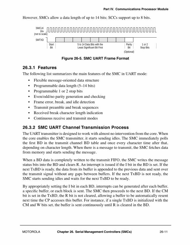
Part IV. Communications Processor Module
However, SMCs allow a data length of up to 14 bits; SCCs support up to 8 bits.
Figure 26-5. SMC UART Frame Format
26.3.1 FeaturesThe following list summarizes the main features of the SMC in UART mode:
¥ Flexible message-oriented data structure¥ Programmable data length (5Ð14 bits) ¥ Programmable 1 or 2 stop bits¥ Even/odd/no parity generation and checking¥ Frame error, break, and idle detection¥ Transmit preamble and break sequences¥ Received break character length indication¥ Continuous receive and transmit modes
26.3.2 SMC UART Channel Transmission ProcessThe UART transmitter is designed to work with almost no intervention from the core. Whenthe core enables the SMC transmitter, it starts sending idles. The SMC immediately pollsthe Þrst BD in the transmit channel BD table and once every character time after that,depending on character length. When there is a message to transmit, the SMC fetches datafrom memory and starts sending the message.
When a BD data is completely written to the transmit FIFO, the SMC writes the messagestatus bits into the BD and clears R. An interrupt is issued if the I bit in the BD is set. If thenext TxBD is ready, the data from its buffer is appended to the previous data and sent overthe transmit signal without any gaps between buffers. If the next TxBD is not ready, theSMC starts sending idles and waits for the next TxBD to be ready.
By appropriately setting the I bit in each BD, interrupts can be generated after each buffer,a speciÞc buffer, or each block is sent. The SMC then proceeds to the next BD. If the CMbit is set in the TxBD, the R bit is not cleared, allowing a buffer to be automatically resentnext time the CP accesses this buffer. For instance, if a single TxBD is initialized with theCM and W bits set, the buffer is sent continuously until R is cleared in the BD.
SMCLK
SMTXD
16x
StartBit
ParityBit
(Optional)
5 to 14 Data Bits with theLeast Significant Bit First
1 or 2Stop Bits
(not to scale)
MOTOROLA Chapter 26. Serial Management Controllers (SMCs) 26-11
Part IV. Communications Processor Module
26.3.3 SMC UART Channel Reception ProcessWhen the core enables the SMC receiver, it enters hunt mode and waits for the Þrstcharacter. The CP then checks the Þrst RxBD to see if it is empty and starts storingcharacters in the buffer. When the buffer is full or the MAX_IDL timer expires (if enabled),the SMC clears the E bit in the BD and generates an interrupt if the I bit in the BD is set. Ifincoming data exceeds the bufferÕs length, the SMC fetches the next BD, and, if it is empty,continues transferring data to this BDÕs buffer. If CM is set in the RxBD, the E bit is notcleared, so the CP can overwrite this buffer on its next access.
26.3.4 Programming the SMC UART ControllerUART mode is selected by setting SMCMR[SM] to 0b10. See Section 26.2.1, ÒSMC ModeRegisters (SMCMR1/SMCMR2).Ó UART mode uses the same data structure as othermodes. This structure supports multibuffer operation and allows break and preamblesequences to be sent. Overrun, parity, and framing errors are reported via the BDs. At itssimplest, the SMC UART controller functions in a character-oriented environment,whereas each character is sent with the selected stop bits and parity. They are received intoseparate 1-byte buffers. A maskable interrupt can be generated when each buffer isreceived.
Many applications can take advantage of the message-oriented capabilities that the SMCUART supports through linked buffers for sending or receiving. Data is handled in amessage-oriented environment, so entire messages can be handled instead of individualcharacters. A message can span several linked buffers; each one can be sent and received asa linked list of buffers without core intervention, which simpliÞes programming and savesprocessor overhead. In a message-oriented environment, an idle sequence is used as themessage delimiter. The transmitter can generate an idle sequence before starting a newmessage and the receiver can close a buffer when an idle sequence is found.
26.3.5 SMC UART Transmit and Receive CommandsTable 26-4 describes transmit commands issued to the CPCR.
Table 26-4. Transmit Commands
Command Description
STOP TRANSMIT
Disables transmission of characters on the transmit channel. If the SMC UART controller receives this command while sending a message, it stops sending. The SMC UART controller Þnishes sending any data that has already been sent to its FIFO and shift register and then stops sending data. The TBPTR is not advanced when this command is issued. The SMC UART controller sends a programmable number of break sequences and then sends idles. The number of break sequences, which can be zero, should be written to the BRKCR before this command is issued to the SMC UART controller.
RESTART TRANSMIT
Enables characters to be sent on the transmit channel. The SMC UART controller expects it after disabling the channel in its SMCMR and after issuing the STOP TRANSMIT command. The SMC UART controller resumes transmission from the current TBPTR in the channelÕs TxBD table.
INIT TX PARAMETERS
Initializes transmit parameters in this serial channelÕs parameter RAM to their reset state and should only be issued when the transmitter is disabled. The INIT TX and RX PARAMETERS command can also be used to reset the transmit and receive parameters.
26-12 MPC8260 PowerQUICC II UserÕs Manual MOTOROLA
Part IV. Communications Processor Module
Table 26-5 describes receive commands issued to the CPCR.
26.3.6 Sending a BreakA break is an all-zeros character without stop bits. It is sent by issuing a STOP TRANSMIT
command. After sending any outstanding data, the SMC sends a character of consecutivezeros, the number of which is the sum of the character length, plus the number of start,parity, and stop bits. The SMC sends a programmable number of break charactersaccording to BRKCR and then reverts to idle or sends data if a RESTART TRANSMIT is issuedbefore completion. When the break completes, the transmitter sends at least one idlecharacter before sending any data to guarantee recognition of a valid start bit.
26.3.7 Sending a PreambleA preamble sequence provides a way to ensure that the line is idle before a new messagetransfer begins. The length of the preamble sequence is constructed of consecutive ones thatare one-character long. If the preamble bit in a BD is set, the SMC sends a preamblesequence before sending that buffer. For 8 data bits, no parity, 1 stop bit, and 1 start bit, apreamble of 10 ones would be sent before the Þrst character in the buffer. If no preamblesequence is sent, data from two ready transmit buffers can be sent on the transmit signalwith no delay between them.
26.3.8 Handling Errors in the SMC UART ControllerThe SMC UART controller reports character reception error conditions via the channelBDs and the SMCE. The SMC UART controller has no transmission errors.
Table 26-5. Receive Commands
Command Description
ENTER HUNT MODE Use the CLOSE RXBD command instead ENTER HUNT MODE for an SMC UART channel.
CLOSE RXBD Forces the SMC to close the current receive BD if it is currently being used and to use the next BD in the list for any subsequently received data. If the SMC is not receiving data, no action is taken.
INIT RX PARAMETERS
Initializes receive parameters in this serial channel parameter RAM to reset state. Issue it only if the receiver is disabled. INIT TX AND RX PARAMETERS resets both receive and transmit parameters.
Table 26-6. SMC UART Errors
Error Description
Overrun The SMC maintains a two-character length FIFO for receiving data. Data is moved to the buffer after the Þrst character is received into the FIFO; if a receiver FIFO overrun occurs, the channel writes the received character into the internal FIFO. It then writes the character to the buffer, closes it, sets the OV bit in the BD, and generates the RXB interrupt if it is enabled. Reception then resumes as normal. Overrun errors that occasionally occur when the line is idle can be ignored.
Parity The channel writes the received character to the buffer, closes it, sets the PR bit in the BD, and generates the RXB interrupt if it is enabled. Reception then resumes as normal.
Idle Sequence Receive
An idle is found when a character of all ones is received, at which point the channel counts consecutive idle characters. If the count reaches MAX_IDL, the buffer is closed and an RXB interrupt is generated. If no receive buffer is open, this does not generate an interrupt or any status information. The idle counter is reset each time a character is received.
MOTOROLA Chapter 26. Serial Management Controllers (SMCs) 26-13
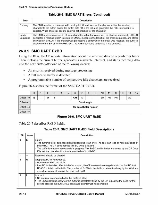
Part IV. Communications Processor Module
26.3.9 SMC UART RxBDUsing the BDs, the CP reports information about the received data on a per-buffer basis.Then it closes the current buffer, generates a maskable interrupt, and starts receiving datainto the next buffer after one of the following occurs:
¥ An error is received during message processing¥ A full receive buffer is detected¥ A programmable number of consecutive idle characters are received
Figure 26-6 shows the format of the SMC UART RxBD.
Table 26-7 describes RxBD Þelds.
Framing The SMC received a character with no stop bit. When it occurs, the channel writes the received character to the buffer, closes the buffer, sets FR in the BD, and generates the RXB interrupt if it is enabled. When this error occurs, parity is not checked for the character.
Break Sequence
The SMC receiver received an all-zero character with a framing error. The channel increments BRKEC, generates a maskable BRK interrupt in SMCE, measures the length of the break sequence, and stores this value in BRKLN. If the channel was processing a buffer when the break was received, the buffer is closed with the BR bit in the RxBD set. The RXB interrupt is generated if it is enabled.
0 1 2 3 4 5 6 7 8 9 10 11 12 13 14 15
Offset + 0 E Ñ W I Ñ CM ID Ñ BR FR PR Ñ OV Ñ
Offset + 2 Data Length
Offset + 4 Rx Data Buffer Pointer
Offset + 6
Figure 26-6. SMC UART RxBD
Table 26-7. SMC UART RxBD Field Descriptions
Bit Name Description
0 E Empty. 0 The buffer is full or data reception stopped due to an error. The core can read or write any Þelds of
this RxBD. The CP does not use this BD while E is zero.1 The buffer is empty or reception is in progress. This RxBD and its buffer are owned by the CP. Once
E is set, the core should not write any Þelds of this RxBD.
1 Ñ Reserved, should be cleared.
2 W Wrap (last BD in RxBD table). 0 Not the last BD in the table. 1 Last BD in the table. After this buffer is used, the CP receives incoming data into the Þrst BD that
RBASE points to in the table. The number of RxBDs in this table is determined only by the W bit and overall space constraints of the dual-port RAM.
3 I Interrupt. 0 No interrupt is generated after this buffer is Þlled.1 The SMCE[RXB] is set when this buffer is completely Þlled by the CP, indicating the need for the
core to process the buffer. RXB can cause an interrupt if it is enabled.
Table 26-6. SMC UART Errors (Continued)
Error Description
26-14 MPC8260 PowerQUICC II UserÕs Manual MOTOROLA
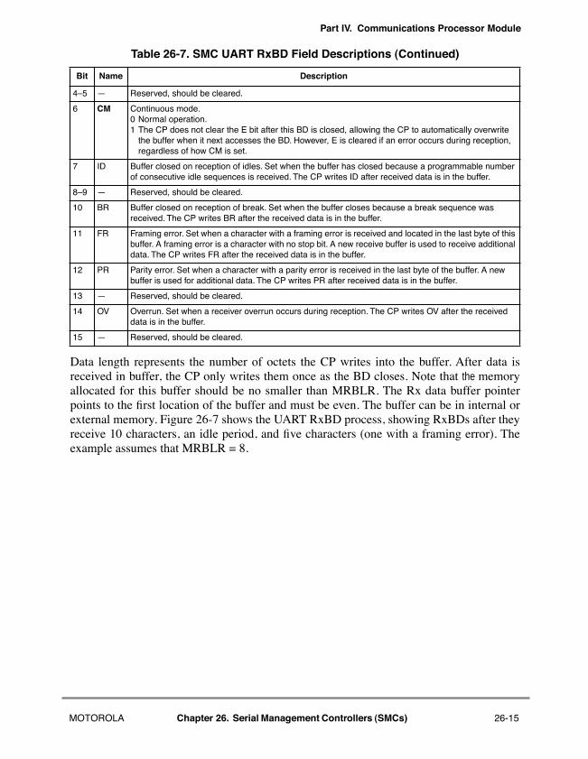
Part IV. Communications Processor Module
Data length represents the number of octets the CP writes into the buffer. After data isreceived in buffer, the CP only writes them once as the BD closes. Note that the memoryallocated for this buffer should be no smaller than MRBLR. The Rx data buffer pointerpoints to the Þrst location of the buffer and must be even. The buffer can be in internal orexternal memory. Figure 26-7 shows the UART RxBD process, showing RxBDs after theyreceive 10 characters, an idle period, and Þve characters (one with a framing error). Theexample assumes that MRBLR = 8.
4Ð5 Ñ Reserved, should be cleared.
6 CM Continuous mode. 0 Normal operation.1 The CP does not clear the E bit after this BD is closed, allowing the CP to automatically overwrite
the buffer when it next accesses the BD. However, E is cleared if an error occurs during reception, regardless of how CM is set.
7 ID Buffer closed on reception of idles. Set when the buffer has closed because a programmable number of consecutive idle sequences is received. The CP writes ID after received data is in the buffer.
8Ð9 Ñ Reserved, should be cleared.
10 BR Buffer closed on reception of break. Set when the buffer closes because a break sequence was received. The CP writes BR after the received data is in the buffer.
11 FR Framing error. Set when a character with a framing error is received and located in the last byte of this buffer. A framing error is a character with no stop bit. A new receive buffer is used to receive additional data. The CP writes FR after the received data is in the buffer.
12 PR Parity error. Set when a character with a parity error is received in the last byte of the buffer. A new buffer is used for additional data. The CP writes PR after received data is in the buffer.
13 Ñ Reserved, should be cleared.
14 OV Overrun. Set when a receiver overrun occurs during reception. The CP writes OV after the received data is in the buffer.
15 Ñ Reserved, should be cleared.
Table 26-7. SMC UART RxBD Field Descriptions (Continued)
Bit Name Description
MOTOROLA Chapter 26. Serial Management Controllers (SMCs) 26-15
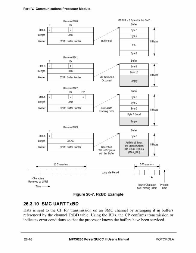
Part IV. Communications Processor Module
Figure 26-7. RxBD Example
26.3.10 SMC UART TxBDData is sent to the CP for transmission on an SMC channel by arranging it in buffersreferenced by the channel TxBD table. Using the BDs, the CP confirms transmission orindicates error conditions so that the processor knows the buffers have been serviced.
Byte 5
Buffer
0
0008
32-Bit Buffer Pointer
0
E IDReceive BD 0
Status
Length
Pointer
0
0002
32-Bit Buffer Pointer
1
E IDReceive BD 1
Status
Length
Pointer
0
0004
32-Bit Buffer Pointer
0
E IDReceive BD 2
Status
Length
Pointer
1
XXXX
32-Bit Buffer Pointer
EReceive BD 3
Status
Length
Pointer
Byte 1
Byte 2
Byte 8
Buffer
Byte 9
Byte 10
Buffer
Byte 1
Byte 2
Byte 3
Buffer
Byte 4 Error!
Empty
Additional Bytesare Stored UnlessIdle Count Expires
(MAX_IDL)
8 Bytes
8 Bytes
8 Bytes
8 Bytes
CharactersReceived by UART
Fourth Character
10 Characters
Long Idle Period
has Framing Error!Present
TimeTime
5 Characters
Buffer Full
Idle Time-OutOccurred
Byte 4 hasFraming Error
ReceptionStill in Progresswith this Buffer
1
FR
etc.
Empty
MRBLR = 8 Bytes for this SMC
26-16 MPC8260 PowerQUICC II UserÕs Manual MOTOROLA
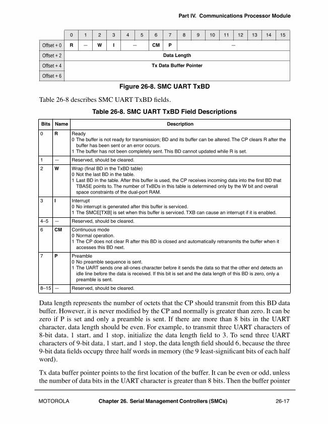
Part IV. Communications Processor Module
Table 26-8 describes SMC UART TxBD Þelds.
Data length represents the number of octets that the CP should transmit from this BD databuffer. However, it is never modiÞed by the CP and normally is greater than zero. It can bezero if P is set and only a preamble is sent. If there are more than 8 bits in the UARTcharacter, data length should be even. For example, to transmit three UART characters of8-bit data, 1 start, and 1 stop, initialize the data length Þeld to 3. To send three UARTcharacters of 9-bit data, 1 start, and 1 stop, the data length Þeld should 6, because the three9-bit data Þelds occupy three half words in memory (the 9 least-signiÞcant bits of each halfword).
Tx data buffer pointer points to the Þrst location of the buffer. It can be even or odd, unlessthe number of data bits in the UART character is greater than 8 bits. Then the buffer pointer
0 1 2 3 4 5 6 7 8 9 10 11 12 13 14 15
Offset + 0 R Ñ W I Ñ CM P Ñ
Offset + 2 Data Length
Offset + 4 Tx Data Buffer Pointer
Offset + 6
Figure 26-8. SMC UART TxBD
Table 26-8. SMC UART TxBD Field Descriptions
Bits Name Description
0 R Ready0 The buffer is not ready for transmission; BD and its buffer can be altered. The CP clears R after the
buffer has been sent or an error occurs.1 The buffer has not been completely sent. This BD cannot updated while R is set.
1 Ñ Reserved, should be cleared.
2 W Wrap (Þnal BD in the TxBD table)0 Not the last BD in the table. 1 Last BD in the table. After this buffer is used, the CP receives incoming data into the Þrst BD that
TBASE points to. The number of TxBDs in this table is determined only by the W bit and overall space constraints of the dual-port RAM.
3 I Interrupt0 No interrupt is generated after this buffer is serviced.1 The SMCE[TXB] is set when this buffer is serviced. TXB can cause an interrupt if it is enabled.
4Ð5 Ñ Reserved, should be cleared.
6 CM Continuous mode0 Normal operation.1 The CP does not clear R after this BD is closed and automatically retransmits the buffer when it
accesses this BD next.
7 P Preamble0 No preamble sequence is sent.1 The UART sends one all-ones character before it sends the data so that the other end detects an
idle line before the data is received. If this bit is set and the data length of this BD is zero, only a preamble is sent.
8Ð15 Ñ Reserved, should be cleared.
MOTOROLA Chapter 26. Serial Management Controllers (SMCs) 26-17
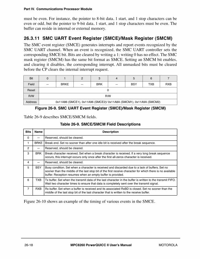
Part IV. Communications Processor Module
must be even. For instance, the pointer to 8-bit data, 1 start, and 1 stop characters can beeven or odd, but the pointer to 9-bit data, 1 start, and 1 stop characters must be even. Thebuffer can reside in internal or external memory.
26.3.11 SMC UART Event Register (SMCE)/Mask Register (SMCM)The SMC event register (SMCE) generates interrupts and report events recognized by theSMC UART channel. When an event is recognized, the SMC UART controller sets thecorresponding SMCE bit. Bits are cleared by writing a 1; writing 0 has no effect. The SMCmask register (SMCM) has the same bit format as SMCE. Setting an SMCM bit enables,and clearing it disables, the corresponding interrupt. All unmasked bits must be clearedbefore the CP clears the internal interrupt request.
Table 26-9 describes SMCE/SMCM Þelds.
Figure 26-10 shows an example of the timing of various events in the SMCE.
Bit 0 1 2 3 4 5 6 7
Field Ñ BRKE Ñ BRK Ñ BSY TXB RXB
Reset 0
R/W R/W
Address 0x11A86 (SMCE1), 0x11A96 (SMCE2)/ 0x11A8A (SMCM1), 0x11A9A (SMCM2)
Figure 26-9. SMC UART Event Register (SMCE)/Mask Register (SMCM)
Table 26-9. SMCE/SMCM Field Descriptions
Bits Name Description
0 Ñ Reserved, should be cleared.
1 BRKE Break end. Set no sooner than after one idle bit is received after the break sequence.
2 Ñ Reserved, should be cleared.
3 BRK Break character received. Set when a break character is received. If a very long break sequence occurs, this interrupt occurs only once after the Þrst all-zeros character is received.
4 Ñ Reserved, should be cleared.
5 BSY Busy condition. Set when a character is received and discarded due to a lack of buffers. Set no sooner than the middle of the last stop bit of the Þrst receive character for which there is no available buffer. Reception resumes when an empty buffer is provided.
6 TXB Tx buffer. Set when the transmit data of the last character in the buffer is written to the transmit FIFO. Wait two character times to ensure that data is completely sent over the transmit signal.
7 RXB Rx buffer. Set when a buffer is received and its associated RxBD is closed. Set no sooner than the middle of the last stop bit of the last character that is written to the receive buffer.
26-18 MPC8260 PowerQUICC II UserÕs Manual MOTOROLA
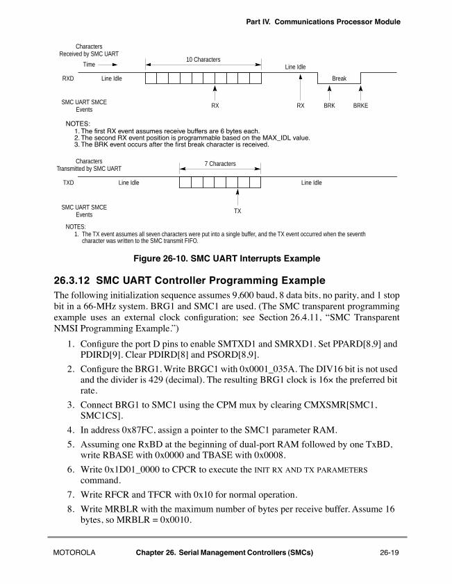
Part IV. Communications Processor Module
Figure 26-10. SMC UART Interrupts Example
26.3.12 SMC UART Controller Programming ExampleThe following initialization sequence assumes 9,600 baud, 8 data bits, no parity, and 1 stopbit in a 66-MHz system. BRG1 and SMC1 are used. (The SMC transparent programmingexample uses an external clock conÞguration; see Section 26.4.11, ÒSMC TransparentNMSI Programming Example.Ó)
1. ConÞgure the port D pins to enable SMTXD1 and SMRXD1. Set PPARD[8,9] and PDIRD[9]. Clear PDIRD[8] and PSORD[8,9].
2. ConÞgure the BRG1. Write BRGC1 with 0x0001_035A. The DIV16 bit is not used and the divider is 429 (decimal). The resulting BRG1 clock is 16´ the preferred bit rate.
3. Connect BRG1 to SMC1 using the CPM mux by clearing CMXSMR[SMC1, SMC1CS].
4. In address 0x87FC, assign a pointer to the SMC1 parameter RAM.
5. Assuming one RxBD at the beginning of dual-port RAM followed by one TxBD, write RBASE with 0x0000 and TBASE with 0x0008.
6. Write 0x1D01_0000 to CPCR to execute the INIT RX AND TX PARAMETERS command.
7. Write RFCR and TFCR with 0x10 for normal operation.
8. Write MRBLR with the maximum number of bytes per receive buffer. Assume 16 bytes, so MRBLR = 0x0010.
RX RX BRK BRKE
Break
Line Idle10 Characters
RXD
CharactersReceived by SMC UART
Time
Line Idle
TXD
CharactersTransmitted by SMC UART
TX
Line Idle Line Idle
7 Characters
NOTES:
SMC UART SMCEEvents
1. The first RX event assumes receive buffers are 6 bytes each.2. The second RX event position is programmable based on the MAX_IDL value.3. The BRK event occurs after the first break character is received.
SMC UART SMCEEvents
NOTES:The TX event assumes all seven characters were put into a single buffer, and the TX event occurred when the seventhcharacter was written to the SMC transmit FIFO.
1.
MOTOROLA Chapter 26. Serial Management Controllers (SMCs) 26-19
Part IV. Communications Processor Module
9. Write MAX_IDL with 0x0000 in the SMC UART-speciÞc parameter RAM to disable the MAX_IDL functionality for this example.
10. Clear BRKLN and BRKEC in the SMC UART-speciÞc parameter RAM.
11. Set BRKCR to 0x0001; if a STOP TRANSMIT COMMAND is issued, one break character is sent.
12. Initialize the RxBD. Assume the Rx data buffer is at 0x0000_1000 in main memory. Write 0xB000 to RxBD[Status and Control], 0x0000 to RxBD[Data Length] (not required), and 0x0000_1000 to RxBD[Buffer Pointer].
13. Assuming the Tx data buffer is at 0x0000_2000 in main memory and contains Þve 8-bit characters, write 0xB000 to TxBD[Status and Control], 0x0005 to TxBD[Data Length], and 0x0000_2000 to TxBD[Buffer Pointer].
14. Write 0xFF to the SMCE1 register to clear any previous events.
15. Write 0x57 to the SMCM1 register to enable all possible SMC1 interrupts.
16. Write 0x0000_1000 to the SIU interrupt mask register low (SIMR_L) so the SMC1 can generate a system interrupt. Write 0xFFFF_FFFF to the SIU interrupt pending register low (SIPNR_L) to clear events.
17. Write 0x4820 to SMCMR to conÞgure normal operation (not loopback), 8-bit characters, no parity, 1 stop bit. The transmitter and receiver are not yet enabled.
18. Write 0x4823 to SMCMR to enable the SMC transmitter and receiver. This additional write ensures that the TEN and REN bits are enabled last.
After 5 bytes are sent, the TxBD is closed. The receive buffer closes after receiving 16bytes. Subsequent data causes a busy (out-of-buffers) condition since only one RxBD isready.
26.4 SMC in Transparent ModeCompared to the SCC in transparent mode, the SMCs generally offer less functionality,which helps them provide simpler functions and slower speeds. Transparent mode isselected by programming SMCMR[SM] to 0b10. Section 26.2.1, ÒSMC Mode Registers(SMCMR1/SMCMR2)Ó describes other protocol-speciÞc bits in the SMCMR. The SMC intransparent mode does not support the following features:
¥ Independent transmit and receive clocks, unless connected to a TDM channel of an SIx
¥ CRC generation and checking
¥ Full RTS, CTS, and CD signals (supports only one SMSYN signal)
¥ Ability to transmit data on demand using the TODR
¥ Receiver/transmitter in transparent mode while executing another protocol
¥ 4-, 8-, or 16-bit SYNC recognition
¥ Internal DPLL support
26-20 MPC8260 PowerQUICC II UserÕs Manual MOTOROLA
Part IV. Communications Processor Module
However, the SMC in transparent mode provides a data character length option of 4 to 16bits, whereas the SCCs provide 8 or 32 bits, depending on GSMR[RFW]. The SMC intransparent mode is also referred to as the SMC transparent controller.
26.4.1 FeaturesThe following list summarizes the features of the SMC in transparent mode:
¥ Flexible data buffers
¥ Connects to a TDM bus using the TSA in an SIx
¥ Transmits and receives transparently on its own set of signals using a sync signal to synchronize the beginning of transmission and reception to an external event
¥ Programmable character length (4Ð16)
¥ Reverse data mode
¥ Continuous transmission and reception modes
¥ Four commands
26.4.2 SMC Transparent Channel Transmission ProcessThe transparent transmitter is designed to work with almost no core intervention. When thecore enables the SMC transmitter in transparent mode, it starts sending idles. The SMCimmediately polls the Þrst BD in the transmit channel BD table and once every charactertime, depending on the character length (every 4 to 16 serial clocks). When there is amessage to transmit, the SMC fetches the data from memory and starts sending the messagewhen synchronization is achieved.
Synchronization can be achieved in two ways. First, when the transmitter is connected to aTDM channel, it can be synchronized to a time slot. Once the frame sync is received, thetransmitter waits for the Þrst bit of its time slot before it starts transmitting. Data is sent onlyduring the time slots deÞned by the TSA. Secondly, when working with its own set ofsignals, the transmitter starts sending when SMSYNx is asserted.
When a BD data is completely written to the transmit FIFO, the L bit is checked and if it isset, the SMC writes the message status bits into the BD and clears the R bit. It then startstransmitting idles. When the end of the current BD is reached and the L bit is not set, onlyR is cleared. In both cases, an interrupt is issued according to the I bit in the BD. Byappropriately setting the I bit in each BD, interrupts can be generated after each buffer, aspeciÞc buffer, or each block is sent. The SMC then proceeds to the next BD. If noadditional buffers have been presented to the SMC for transmission and the L bit wascleared, an underrun is detected and the SMC begins sending idles.
If the CM bit is set in the TxBD, the R bit is not cleared, so the CP can overwrite the bufferon its next access. For instance, if a single TxBD is initialized with the CM and W bits set,the buffer is sent continuously until R is cleared in the BD.
MOTOROLA Chapter 26. Serial Management Controllers (SMCs) 26-21
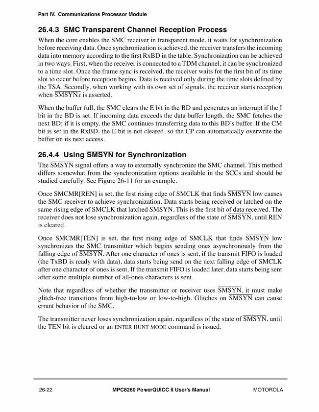
Part IV. Communications Processor Module
26.4.3 SMC Transparent Channel Reception ProcessWhen the core enables the SMC receiver in transparent mode, it waits for synchronizationbefore receiving data. Once synchronization is achieved, the receiver transfers the incomingdata into memory according to the Þrst RxBD in the table. Synchronization can be achievedin two ways. First, when the receiver is connected to a TDM channel, it can be synchronizedto a time slot. Once the frame sync is received, the receiver waits for the Þrst bit of its timeslot to occur before reception begins. Data is received only during the time slots deÞned bythe TSA. Secondly, when working with its own set of signals, the receiver starts receptionwhen SMSYNx is asserted.
When the buffer full, the SMC clears the E bit in the BD and generates an interrupt if the Ibit in the BD is set. If incoming data exceeds the data buffer length, the SMC fetches thenext BD; if it is empty, the SMC continues transferring data to this BDÕs buffer. If the CMbit is set in the RxBD, the E bit is not cleared, so the CP can automatically overwrite thebuffer on its next access.
26.4.4 Using SMSYN for SynchronizationThe SMSYN signal offers a way to externally synchronize the SMC channel. This methoddiffers somewhat from the synchronization options available in the SCCs and should bestudied carefully. See Figure 26-11 for an example.
Once SMCMR[REN] is set, the Þrst rising edge of SMCLK that Þnds SMSYN low causesthe SMC receiver to achieve synchronization. Data starts being received or latched on thesame rising edge of SMCLK that latched SMSYN. This is the Þrst bit of data received. Thereceiver does not lose synchronization again, regardless of the state of SMSYN, until RENis cleared.
Once SMCMR[TEN] is set, the Þrst rising edge of SMCLK that Þnds SMSYN lowsynchronizes the SMC transmitter which begins sending ones asynchronously from thefalling edge of SMSYN. After one character of ones is sent, if the transmit FIFO is loaded(the TxBD is ready with data), data starts being send on the next falling edge of SMCLKafter one character of ones is sent. If the transmit FIFO is loaded later, data starts being sentafter some multiple number of all-ones characters is sent.
Note that regardless of whether the transmitter or receiver uses SMSYN, it must makeglitch-free transitions from high-to-low or low-to-high. Glitches on SMSYN can causeerrant behavior of the SMC.
The transmitter never loses synchronization again, regardless of the state of SMSYN, untilthe TEN bit is cleared or an ENTER HUNT MODE command is issued.
26-22 MPC8260 PowerQUICC II UserÕs Manual MOTOROLA
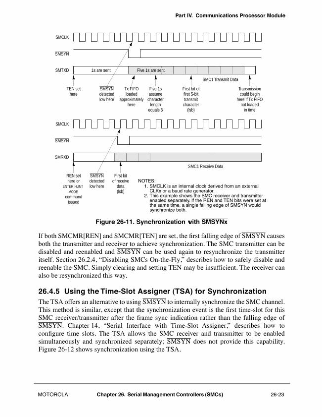
Part IV. Communications Processor Module
Figure 26-11. Synchronization with SMSYNx
If both SMCMR[REN] and SMCMR[TEN] are set, the Þrst falling edge of SMSYN causesboth the transmitter and receiver to achieve synchronization. The SMC transmitter can bedisabled and reenabled and SMSYN can be used again to resynchronize the transmitteritself. Section 26.2.4, ÒDisabling SMCs On-the-Fly,Ó describes how to safely disable andreenable the SMC. Simply clearing and setting TEN may be insufÞcient. The receiver canalso be resynchronized this way.
26.4.5 Using the Time-Slot Assigner (TSA) for SynchronizationThe TSA offers an alternative to using SMSYN to internally synchronize the SMC channel.This method is similar, except that the synchronization event is the Þrst time-slot for thisSMC receiver/transmitter after the frame sync indication rather than the falling edge ofSMSYN. Chapter 14, ÒSerial Interface with Time-Slot Assigner,Ó describes how toconÞgure time slots. The TSA allows the SMC receiver and transmitter to be enabledsimultaneously and synchronized separately; SMSYN does not provide this capability.Figure 26-12 shows synchronization using the TSA.
SMCLK
SMSYN
SMTXD 1s are sent Five 1s are sent
TEN sethere
Tx FIFOloaded
approximatelyhere
Five 1sassume
characterlength
equals 5
First bit offirst 5-bittransmit
character(lsb)
Transmissioncould begin
here if Tx FIFOnot loaded
in time
SMSYNdetectedlow here
SMCLK
SMSYN
SMRXD
REN sethere or
First bitof receive
data(lsb)
SMSYNdetectedlow hereENTER HUNT
MODEcommand
issued
NOTES:SMCLK is an internal clock derived from an externalCLKx or a baud rate generator.
1.
This example shows the SMC receiver and transmitter2.enabled separately. If the REN and TEN bits were set atthe same time, a single falling edge of SMSYN wouldsynchronize both.
SMC1 Transmit Data
SMC1 Receive Data
MOTOROLA Chapter 26. Serial Management Controllers (SMCs) 26-23
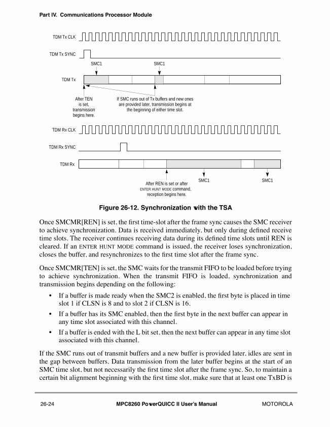
Part IV. Communications Processor Module
Figure 26-12. Synchronization with the TSA
Once SMCMR[REN] is set, the Þrst time-slot after the frame sync causes the SMC receiverto achieve synchronization. Data is received immediately, but only during deÞned receivetime slots. The receiver continues receiving data during its deÞned time slots until REN iscleared. If an ENTER HUNT MODE command is issued, the receiver loses synchronization,closes the buffer, and resynchronizes to the Þrst time slot after the frame sync.
Once SMCMR[TEN] is set, the SMC waits for the transmit FIFO to be loaded before tryingto achieve synchronization. When the transmit FIFO is loaded, synchronization andtransmission begins depending on the following:
¥ If a buffer is made ready when the SMC2 is enabled, the Þrst byte is placed in time slot 1 if CLSN is 8 and to slot 2 if CLSN is 16.
¥ If a buffer has its SMC enabled, then the Þrst byte in the next buffer can appear in any time slot associated with this channel.
¥ If a buffer is ended with the L bit set, then the next buffer can appear in any time slot associated with this channel.
If the SMC runs out of transmit buffers and a new buffer is provided later, idles are sent inthe gap between buffers. Data transmission from the later buffer begins at the start of anSMC time slot, but not necessarily the Þrst time slot after the frame sync. So, to maintain acertain bit alignment beginning with the Þrst time slot, make sure that at least one TxBD is
TDM Tx CLK
TDM Tx SYNC
TDM Tx
After TEN If SMC runs out of Tx buffers and new onesare provided later, transmission begins atis set,
transmissionbegins here.
the beginning of either time slot.
SMC1SMC1
TDM Rx CLK
TDM Rx SYNC
TDM Rx
After REN is set or afterENTER HUNT MODE command,
reception begins here.
SMC1 SMC1
26-24 MPC8260 PowerQUICC II UserÕs Manual MOTOROLA
Part IV. Communications Processor Module
always ready and that underruns do not occur. Otherwise, the SMC transmitter should bedisabled and reenabled. Section 26.2.4, ÒDisabling SMCs On-the-Fly,Ó describes how tosafely disable and reenable the SMC. Simply clearing and setting TEN may not be enough.
26.4.6 SMC Transparent CommandsTable 26-10 describes transmit commands issued to the CPCR.
Table 26-11 describes receive commands issued to the CPCR.
26.4.7 Handling Errors in the SMC Transparent ControllerThe SMC uses BDs and the SMCE to report message send and receive errors.
Table 26-10. SMC Transparent Transmit Commands
Command Description
STOP TRANSMIT
After hardware or software is reset and the channel is enabled in the SMCM, the channel is in transmit enable mode and polls the Þrst BD. This command disables transmission of frames on the transmit channel. If the transparent controller receives this command while sending a frame, it stops after the contents of the FIFO are sent (up to 2 characters). The TBPTR is not advanced to the next BD, no new BD is accessed, and no new buffers are sent for this channel. The transmitter sends idles until a RESTART TRANSMIT command is issued.
RESTART TRANSMIT
Starts or resumes transmission from the current TBPTR in the channel TxBD table. When the channel receives this command, it polls the R bit in this BD. The SMC expects this command after a STOP TRANSMIT is issued. The channel in its mode register is disabled or after a transmitter error occurs.
INIT TX PARAMETERS
Initializes transmit parameters in this serial channel to reset state. Use only if the transmitter is disabled. The INIT TX AND RX PARAMETERS command resets transmit and receive parameters.
Table 26-11. SMC Transparent Receive Commands
Command Description
ENTER HUNT MODE
Forces the SMC to close the current receive BD if it is in use and to use the next BD for subsequent data. If the SMC is not receiving data, the buffer is not closed. Additionally, this command causes the receiver to wait for a resynchronization before reception resumes.
CLOSE RXBD Forces the SMC to close the current receive BD if it in use and to use the next BD in the list for subsequent received data. If the SMC is not in the process of receiving data, no action is taken.
iNIT RX PARAMETERS
Initializes receive parameters in this serial channel to reset state. Use only if the receiver is disabled. The INIT TX AND RX PARAMETERS command resets receive and transmit parameters.
Table 26-12. SMC Transparent Error Conditions
Error Descriptions
Underrun The channel stops sending the buffer, closes it, sets UN in the BD, and generates a TXE interrupt if it is enabled. The channel resumes sending after a RESTART TRANSMIT command. Underrun cannot occur between frames.
Overrun The SMC maintains an internal FIFO for receiving data. If the buffer is in external memory, the CP begins programming the SDMA channel when the Þrst character is received into the FIFO. If a FIFO overrun occurs, the SMC writes the received data character over the previously received character. The previous character and its status bits are lost. Then the channel closes the buffer, sets OV in the BD, and generates the RXB interrupt if it is enabled. Reception continues as normal.
MOTOROLA Chapter 26. Serial Management Controllers (SMCs) 26-25
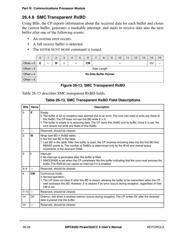
Part IV. Communications Processor Module
26.4.8 SMC Transparent RxBDUsing BDs, the CP reports information about the received data for each buffer and closesthe current buffer, generates a maskable interrupt, and starts to receive data into the nextbuffer after one of the following events:
¥ An overrun error occurs.¥ A full receive buffer is detected.¥ The ENTER HUNT MODE command is issued.
Table 26-13 describes SMC transparent RxBD Þelds.
0 1 2 3 4 5 6 7 8 9 10 11 12 13 14 15
Offset + 0 E Ñ W I Ñ CM Ñ OV Ñ
Offset + 2 Data Length
Offset + 4 Rx Data Buffer Pointer
Offset + 6
Figure 26-13. SMC Transparent RxBD
Table 26-13. SMC Transparent RxBD Field Descriptions
Bits Name Description
0 E Empty. 0 The buffer is full or reception was aborted due to an error. The core can read or write any Þelds of
this RxBD. The CP does not use this BD while E = 0.1 The buffer is empty or is receiving data. The CP owns this RxBD and its buffer. Once E is set, the
core should not write any Þelds of this RxBD.
1 Ñ Reserved, should be cleared.
2 W Wrap (last BD in RxBD table). 0 Not the last BD in the table. 1 Last BD in the table. After this buffer is used, the CP receives incoming data into the Þrst BD that
RBASE points to. The number of RxBDs is determined only by the W bit and overall space constraints of the dual-port RAM.
3 I Interrupt. 0 No interrupt is generated after this buffer is Þlled.1 SMCE[RXB] is set when the CP completely Þlls this buffer indicating that the core must process the
buffer. The RXB bit can cause an interrupt if it is enabled.
4Ð5 Ñ Reserved, should be cleared.
6 CM Continuous mode. 0 Normal operation.1 The CP does not clear E after this BD is closed, allowing the buffer to be overwritten when the CP
next accesses this BD. However, E is cleared if an error occurs during reception, regardless of how CM is set.
7Ð13 Ñ Reserved, should be cleared.
14 OV Overrun. Set when a receiver overrun occurs during reception. The CP writes OV after the received data is placed into the buffer.
15 Ñ Reserved, should be cleared.
26-26 MPC8260 PowerQUICC II UserÕs Manual MOTOROLA
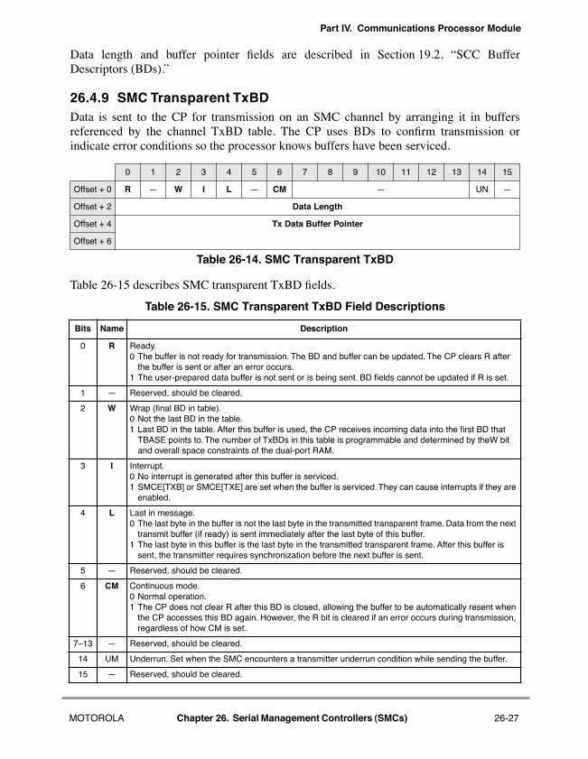
Part IV. Communications Processor Module
Data length and buffer pointer Þelds are described in Section 19.2, ÒSCC BufferDescriptors (BDs).Ó
26.4.9 SMC Transparent TxBDData is sent to the CP for transmission on an SMC channel by arranging it in buffersreferenced by the channel TxBD table. The CP uses BDs to conÞrm transmission orindicate error conditions so the processor knows buffers have been serviced.
Table 26-15 describes SMC transparent TxBD Þelds.
0 1 2 3 4 5 6 7 8 9 10 11 12 13 14 15
Offset + 0 R Ñ W I L Ñ CM Ñ UN Ñ
Offset + 2 Data Length
Offset + 4 Tx Data Buffer Pointer
Offset + 6
Table 26-14. SMC Transparent TxBD
Table 26-15. SMC Transparent TxBD Field Descriptions
Bits Name Description
0 R Ready. 0 The buffer is not ready for transmission. The BD and buffer can be updated. The CP clears R after
the buffer is sent or after an error occurs.1 The user-prepared data buffer is not sent or is being sent. BD Þelds cannot be updated if R is set.
1 Ñ Reserved, should be cleared.
2 W Wrap (Þnal BD in table). 0 Not the last BD in the table. 1 Last BD in the table. After this buffer is used, the CP receives incoming data into the Þrst BD that
TBASE points to. The number of TxBDs in this table is programmable and determined by theW bit and overall space constraints of the dual-port RAM.
3 I Interrupt. 0 No interrupt is generated after this buffer is serviced.1 SMCE[TXB] or SMCE[TXE] are set when the buffer is serviced. They can cause interrupts if they are
enabled.
4 L Last in message. 0 The last byte in the buffer is not the last byte in the transmitted transparent frame. Data from the next
transmit buffer (if ready) is sent immediately after the last byte of this buffer. 1 The last byte in this buffer is the last byte in the transmitted transparent frame. After this buffer is
sent, the transmitter requires synchronization before the next buffer is sent.
5 Ñ Reserved, should be cleared.
6 CM Continuous mode. 0 Normal operation.1 The CP does not clear R after this BD is closed, allowing the buffer to be automatically resent when
the CP accesses this BD again. However, the R bit is cleared if an error occurs during transmission, regardless of how CM is set.
7Ð13 Ñ Reserved, should be cleared.
14 UM Underrun. Set when the SMC encounters a transmitter underrun condition while sending the buffer.
15 Ñ Reserved, should be cleared.
MOTOROLA Chapter 26. Serial Management Controllers (SMCs) 26-27
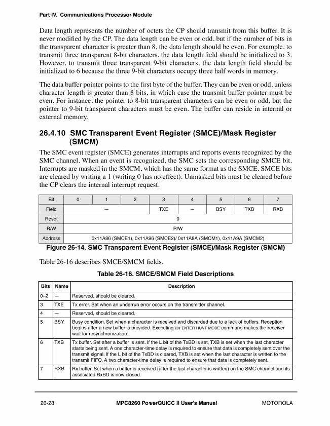
Part IV. Communications Processor Module
Data length represents the number of octets the CP should transmit from this buffer. It isnever modiÞed by the CP. The data length can be even or odd, but if the number of bits inthe transparent character is greater than 8, the data length should be even. For example, totransmit three transparent 8-bit characters, the data length Þeld should be initialized to 3.However, to transmit three transparent 9-bit characters, the data length Þeld should beinitialized to 6 because the three 9-bit characters occupy three half words in memory.
The data buffer pointer points to the Þrst byte of the buffer. They can be even or odd, unlesscharacter length is greater than 8 bits, in which case the transmit buffer pointer must beeven. For instance, the pointer to 8-bit transparent characters can be even or odd, but thepointer to 9-bit transparent characters must be even. The buffer can reside in internal orexternal memory.
26.4.10 SMC Transparent Event Register (SMCE)/Mask Register (SMCM)
The SMC event register (SMCE) generates interrupts and reports events recognized by theSMC channel. When an event is recognized, the SMC sets the corresponding SMCE bit.Interrupts are masked in the SMCM, which has the same format as the SMCE. SMCE bitsare cleared by writing a 1 (writing 0 has no effect). Unmasked bits must be cleared beforethe CP clears the internal interrupt request.
Table 26-16 describes SMCE/SMCM Þelds.
Bit 0 1 2 3 4 5 6 7
Field Ñ TXE Ñ BSY TXB RXB
Reset 0
R/W R/W
Address 0x11A86 (SMCE1), 0x11A96 (SMCE2)/ 0x11A8A (SMCM1), 0x11A9A (SMCM2)
Figure 26-14. SMC Transparent Event Register (SMCE)/Mask Register (SMCM)
Table 26-16. SMCE/SMCM Field Descriptions
Bits Name Description
0Ð2 Ñ Reserved, should be cleared.
3 TXE Tx error. Set when an underrun error occurs on the transmitter channel.
4 Ñ Reserved, should be cleared.
5 BSY Busy condition. Set when a character is received and discarded due to a lack of buffers. Reception begins after a new buffer is provided. Executing an ENTER HUNT MODE command makes the receiver wait for resynchronization.
6 TXB Tx buffer. Set after a buffer is sent. If the L bit of the TxBD is set, TXB is set when the last character starts being sent. A one character-time delay is required to ensure that data is completely sent over the transmit signal. If the L bit of the TxBD is cleared, TXB is set when the last character is written to the transmit FIFO. A two character-time delay is required to ensure that data is completely sent.
7 RXB Rx buffer. Set when a buffer is received (after the last character is written) on the SMC channel and its associated RxBD is now closed.
26-28 MPC8260 PowerQUICC II UserÕs Manual MOTOROLA
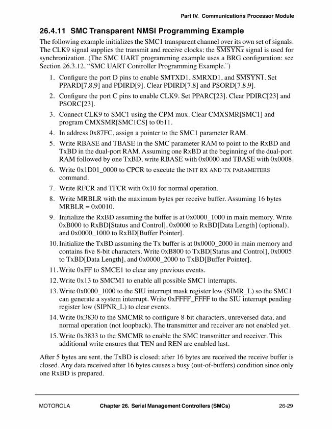
Part IV. Communications Processor Module
26.4.11 SMC Transparent NMSI Programming ExampleThe following example initializes the SMC1 transparent channel over its own set of signals.The CLK9 signal supplies the transmit and receive clocks; the SMSYNx signal is used forsynchronization. (The SMC UART programming example uses a BRG conÞguration; seeSection 26.3.12, ÒSMC UART Controller Programming Example.Ó)
1. ConÞgure the port D pins to enable SMTXD1, SMRXD1, and SMSYN1. Set PPARD[7,8,9] and PDIRD[9]. Clear PDIRD[7,8] and PSORD[7,8,9].
2. ConÞgure the port C pins to enable CLK9. Set PPARC[23]. Clear PDIRC[23] and PSORC[23].
3. Connect CLK9 to SMC1 using the CPM mux. Clear CMXSMR[SMC1] and program CMXSMR[SMC1CS] to 0b11.
4. In address 0x87FC, assign a pointer to the SMC1 parameter RAM.
5. Write RBASE and TBASE in the SMC parameter RAM to point to the RxBD and TxBD in the dual-port RAM. Assuming one RxBD at the beginning of the dual-port RAM followed by one TxBD, write RBASE with 0x0000 and TBASE with 0x0008.
6. Write 0x1D01_0000 to CPCR to execute the INIT RX AND TX PARAMETERS command.
7. Write RFCR and TFCR with 0x10 for normal operation.
8. Write MRBLR with the maximum bytes per receive buffer. Assuming 16 bytes MRBLR = 0x0010.
9. Initialize the RxBD assuming the buffer is at 0x0000_1000 in main memory. Write 0xB000 to RxBD[Status and Control], 0x0000 to RxBD[Data Length] (optional), and 0x0000_1000 to RxBD[Buffer Pointer].
10. Initialize the TxBD assuming the Tx buffer is at 0x0000_2000 in main memory and contains Þve 8-bit characters. Write 0xB800 to TxBD[Status and Control], 0x0005 to TxBD[Data Length], and 0x0000_2000 to TxBD[Buffer Pointer].
11. Write 0xFF to SMCE1 to clear any previous events.
12. Write 0x13 to SMCM1 to enable all possible SMC1 interrupts.
13. Write 0x0000_1000 to the SIU interrupt mask register low (SIMR_L) so the SMC1 can generate a system interrupt. Write 0xFFFF_FFFF to the SIU interrupt pending register low (SIPNR_L) to clear events.
14. Write 0x3830 to the SMCMR to conÞgure 8-bit characters, unreversed data, and normal operation (not loopback). The transmitter and receiver are not enabled yet.
15. Write 0x3833 to the SMCMR to enable the SMC transmitter and receiver. This additional write ensures that TEN and REN are enabled last.
After 5 bytes are sent, the TxBD is closed; after 16 bytes are received the receive buffer isclosed. Any data received after 16 bytes causes a busy (out-of-buffers) condition since onlyone RxBD is prepared.
MOTOROLA Chapter 26. Serial Management Controllers (SMCs) 26-29
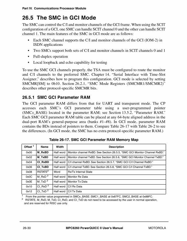
Part IV. Communications Processor Module
26.5 The SMC in GCI ModeThe SMC can control the C/I and monitor channels of the GCI frame. When using the SCITconÞguration of a GCI, one SMC can handle SCIT channel 0 and the other can handle SCITchannel 1. The main features of the SMC in GCI mode are as follows:
¥ Each SMC channel supports the C/I and monitor channels of the GCI (IOM-2) in ISDN applications
¥ Two SMCs support both sets of C/I and monitor channels in SCIT channels 0 and 1
¥ Full-duplex operation
¥ Local loopback and echo capability for testing
To use the SMC GCI channels properly, the TSA must be conÞgured to route the monitorand C/I channels to the preferred SMC. Chapter 14, ÒSerial Interface with Time-SlotAssigner,Ó describes how to program this conÞguration. GCI mode is selected by settingSMCMR[SM] to 0b10. Section 26.2.1, ÒSMC Mode Registers (SMCMR1/SMCMR2)Ódescribes other protocol-speciÞc SMCMR bits.
26.5.1 SMC GCI Parameter RAMThe GCI parameter RAM differs from that for UART and transparent mode. The CPaccesses each SMCÕs GCI parameter table using a user-programmed pointer(SMCx_BASE) located in the parameter RAM; see Section 13.5.2, ÒParameter RAM.ÓEach SMC GCI parameter RAM table can be placed at any 64-byte aligned address in thedual-port RAMÕs general-purpose area (banks #1Ð#8). In GCI mode, parameter RAMcontains the BDs instead of pointers to them. Compare Table 26-17 with Table 26-2 to seethe differences. (In GCI mode, the SMC has no extra protocol-speciÞc parameter RAM.)
Table 26-17. SMC GCI Parameter RAM Memory Map
Offset 1
1 From the pointer value programmed in SMCx_BASE: SMC1_BASE at 0x87FC, SMC2_BASE at 0x88FC.
Name Width Description
0x00 M_RxBD Half word Monitor channel RxBD. See Section 26.5.5, ÒSMC GCI Monitor Channel RxBD.Ó
0x02 M_TxBD Half word Monitor channel TxBD. See Section 26.5.6, ÒSMC GCI Monitor Channel TxBD.Ó
0x04 CI_RxBD Half word C/I channel RxBD. See Section 26.5.7, ÒSMC GCI C/I Channel RxBD.Ó
0x06 CI_TxBD Half word C/I channel TxBD. See Section 26.5.8, ÒSMC GCI C/I Channel TxBD.Ó
0x08 RSTATE2
2 RSTATE, M_RxD, M_TxD, CI_RxD, and CI_TxD do not need to be accessed by the user in normal operation, and are reserved for RISC use only.
Word Rx/Tx Internal State
0x0C M_RxD 2 Half word Monitor Rx Data
0x0E M_TxD 2 Half word Monitor Tx Data
0x10 CI_RxD 2 Half word C/I Rx Data
0x12 CI_TxD 2 Half word C/I Tx Data
26-30 MPC8260 PowerQUICC II UserÕs Manual MOTOROLA
Part IV. Communications Processor Module
26.5.2 Handling the GCI Monitor ChannelThe following sections describe how the GCI monitor channel is handled.
26.5.2.1 SMC GCI Monitor Channel Transmission ProcessMonitor channel 0 is used to exchange data with a layer 1 device (reading and writinginternal registers and transferring of the S and Q bits). Monitor channel 1 is used forprogramming and controlling voice/data modules such as CODECs. The core writes thebyte into the TxBD. The SMC sends the data on the monitor channel and handles the A andE control bits according to the GCI monitor channel protocol. The TIMEOUT commandresolves deadlocks when errors in the A and E bit states occur on the data line.
26.5.2.2 SMC GCI Monitor Channel Reception ProcessThe SMC receives data and handles the A and E control bits according to the GCI monitorchannel protocol. When the CP stores a received data byte in the SMC RxBD, a maskableinterrupt is generated. A TRANSMIT ABORT REQUEST command causes the MPC8260 tosend an abort request on the E bit.
26.5.3 Handling the GCI C/I ChannelThe C/I channel is used to control the layer 1 device. The layer 2 device in the TE sendscommands and receives indication to or from the upstream layer 1 device through C/Ichannel 0. In the SCIT conÞguration, C/I channel 1 is used to convey real-time statusinformation between the layer 2 device and nonlayer 1 peripheral devices (CODECs).
26.5.3.1 SMC GCI C/I Channel Transmission ProcessThe core writes the data byte into the C/I TxBD and the SMC transmits the datacontinuously on the C/I channel to the physical layer device.
26.5.3.2 SMC GCI C/I Channel Reception ProcessThe SMC receiver continuously monitors the C/I channel. When it recognizes a change inthe data and this value is received in two successive frames, it is interpreted as valid data.This is called the double last-look method. The CP stores the received data byte in the C/IRxBD and a maskable interrupt is generated. If the SMC is conÞgured to support SCITchannel 1, the double last-look method is not used.
MOTOROLA Chapter 26. Serial Management Controllers (SMCs) 26-31
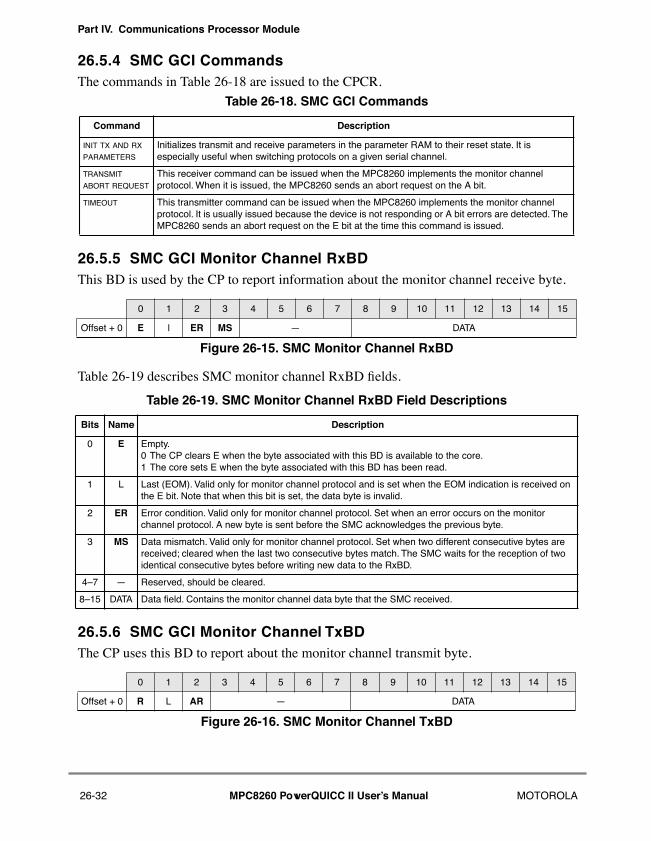
Part IV. Communications Processor Module
26.5.4 SMC GCI CommandsThe commands in Table 26-18 are issued to the CPCR.
26.5.5 SMC GCI Monitor Channel RxBDThis BD is used by the CP to report information about the monitor channel receive byte.
Table 26-19 describes SMC monitor channel RxBD Þelds.
26.5.6 SMC GCI Monitor Channel TxBDThe CP uses this BD to report about the monitor channel transmit byte.
Table 26-18. SMC GCI Commands
Command Description
INIT TX AND RX PARAMETERS
Initializes transmit and receive parameters in the parameter RAM to their reset state. It is especially useful when switching protocols on a given serial channel.
TRANSMIT ABORT REQUEST
This receiver command can be issued when the MPC8260 implements the monitor channel protocol. When it is issued, the MPC8260 sends an abort request on the A bit.
TIMEOUT This transmitter command can be issued when the MPC8260 implements the monitor channel protocol. It is usually issued because the device is not responding or A bit errors are detected. The MPC8260 sends an abort request on the E bit at the time this command is issued.
0 1 2 3 4 5 6 7 8 9 10 11 12 13 14 15
Offset + 0 E l ER MS Ñ DATA
Figure 26-15. SMC Monitor Channel RxBD
Table 26-19. SMC Monitor Channel RxBD Field Descriptions
Bits Name Description
0 E Empty. 0 The CP clears E when the byte associated with this BD is available to the core.1 The core sets E when the byte associated with this BD has been read.
1 L Last (EOM). Valid only for monitor channel protocol and is set when the EOM indication is received on the E bit. Note that when this bit is set, the data byte is invalid.
2 ER Error condition. Valid only for monitor channel protocol. Set when an error occurs on the monitor channel protocol. A new byte is sent before the SMC acknowledges the previous byte.
3 MS Data mismatch. Valid only for monitor channel protocol. Set when two different consecutive bytes are received; cleared when the last two consecutive bytes match. The SMC waits for the reception of two identical consecutive bytes before writing new data to the RxBD.
4Ð7 Ñ Reserved, should be cleared.
8Ð15 DATA Data Þeld. Contains the monitor channel data byte that the SMC received.
0 1 2 3 4 5 6 7 8 9 10 11 12 13 14 15
Offset + 0 R L AR Ñ DATA
Figure 26-16. SMC Monitor Channel TxBD
26-32 MPC8260 PowerQUICC II UserÕs Manual MOTOROLA
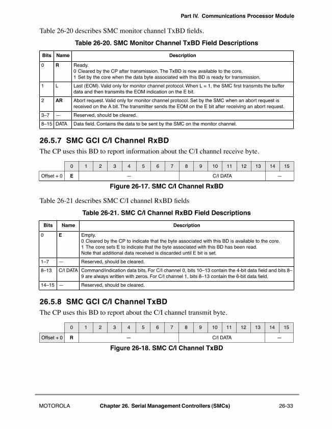
Part IV. Communications Processor Module
Table 26-20 describes SMC monitor channel TxBD Þelds.
26.5.7 SMC GCI C/I Channel RxBDThe CP uses this BD to report information about the C/I channel receive byte.
Table 26-21 describes SMC C/I channel RxBD Þelds
26.5.8 SMC GCI C/I Channel TxBDThe CP uses this BD to report about the C/I channel transmit byte.
Table 26-20. SMC Monitor Channel TxBD Field Descriptions
Bits Name Description
0 R Ready. 0 Cleared by the CP after transmission. The TxBD is now available to the core.1 Set by the core when the data byte associated with this BD is ready for transmission.
1 L Last (EOM). Valid only for monitor channel protocol. When L = 1, the SMC Þrst transmits the buffer data and then transmits the EOM indication on the E bit.
2 AR Abort request. Valid only for monitor channel protocol. Set by the SMC when an abort request is received on the A bit. The transmitter sends the EOM on the E bit after receiving an abort request.
3Ð7 Ñ Reserved, should be cleared.
8Ð15 DATA Data Þeld. Contains the data to be sent by the SMC on the monitor channel.
0 1 2 3 4 5 6 7 8 9 10 11 12 13 14 15
Offset + 0 E Ñ C/I DATA Ñ
Figure 26-17. SMC C/I Channel RxBD
Table 26-21. SMC C/I Channel RxBD Field Descriptions
Bits Name Description
0 E Empty. 0 Cleared by the CP to indicate that the byte associated with this BD is available to the core.1 The core sets E to indicate that the byte associated with this BD has been read.Note that additional data received is discarded until E bit is set.
1Ð7 Ñ Reserved, should be cleared.
8Ð13 C/I DATA Command/indication data bits. For C/I channel 0, bits 10Ð13 contain the 4-bit data Þeld and bits 8Ð9 are always written with zeros. For C/I channel 1, bits 8Ð13 contain the 6-bit data Þeld.
14Ð15 Ñ Reserved, should be cleared.
0 1 2 3 4 5 6 7 8 9 10 11 12 13 14 15
Offset + 0 R Ñ C/I DATA Ñ
Figure 26-18. SMC C/I Channel TxBD
MOTOROLA Chapter 26. Serial Management Controllers (SMCs) 26-33
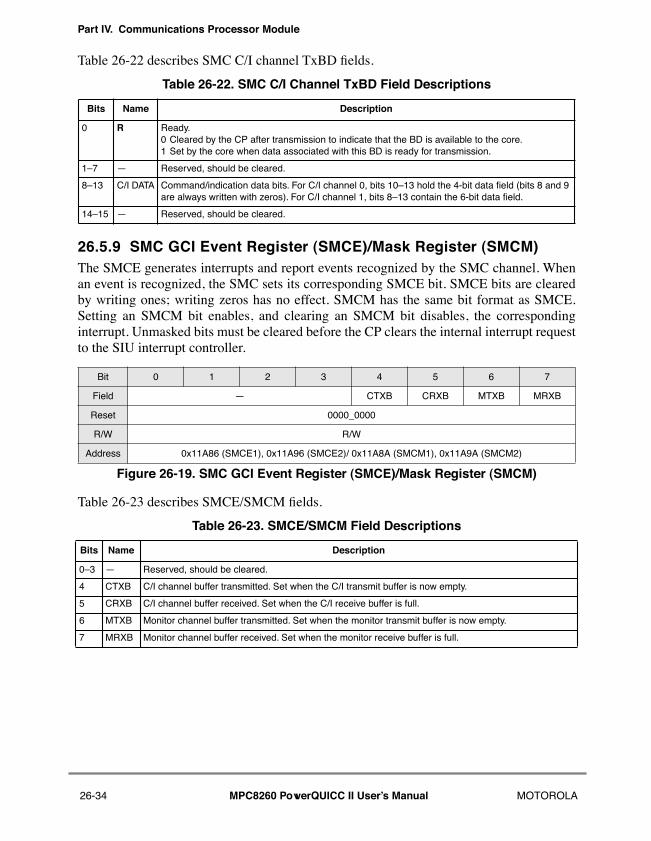
Part IV. Communications Processor Module
Table 26-22 describes SMC C/I channel TxBD Þelds.
26.5.9 SMC GCI Event Register (SMCE)/Mask Register (SMCM)The SMCE generates interrupts and report events recognized by the SMC channel. Whenan event is recognized, the SMC sets its corresponding SMCE bit. SMCE bits are clearedby writing ones; writing zeros has no effect. SMCM has the same bit format as SMCE.Setting an SMCM bit enables, and clearing an SMCM bit disables, the correspondinginterrupt. Unmasked bits must be cleared before the CP clears the internal interrupt requestto the SIU interrupt controller.
Table 26-23 describes SMCE/SMCM Þelds.
Table 26-22. SMC C/I Channel TxBD Field Descriptions
Bits Name Description
0 R Ready. 0 Cleared by the CP after transmission to indicate that the BD is available to the core.1 Set by the core when data associated with this BD is ready for transmission.
1Ð7 Ñ Reserved, should be cleared.
8Ð13 C/I DATA Command/indication data bits. For C/I channel 0, bits 10Ð13 hold the 4-bit data Þeld (bits 8 and 9 are always written with zeros). For C/I channel 1, bits 8Ð13 contain the 6-bit data Þeld.
14Ð15 Ñ Reserved, should be cleared.
Bit 0 1 2 3 4 5 6 7
Field Ñ CTXB CRXB MTXB MRXB
Reset 0000_0000
R/W R/W
Address 0x11A86 (SMCE1), 0x11A96 (SMCE2)/ 0x11A8A (SMCM1), 0x11A9A (SMCM2)
Figure 26-19. SMC GCI Event Register (SMCE)/Mask Register (SMCM)
Table 26-23. SMCE/SMCM Field Descriptions
Bits Name Description
0Ð3 Ñ Reserved, should be cleared.
4 CTXB C/I channel buffer transmitted. Set when the C/I transmit buffer is now empty.
5 CRXB C/I channel buffer received. Set when the C/I receive buffer is full.
6 MTXB Monitor channel buffer transmitted. Set when the monitor transmit buffer is now empty.
7 MRXB Monitor channel buffer received. Set when the monitor receive buffer is full.
26-34 MPC8260 PowerQUICC II UserÕs Manual MOTOROLA
Chapter 27 Multi-Channel Controllers (MCCs)270270
The MPC8260Õs two multi-channel controllers (MCC1 and MCC2) each handle up to 128serial, full-duplex data channels. The 128 channels are divided into four subgroups (of 32channels each). One or more subgroups can be multiplexed through corresponding SIxTDM channels; MCC1 connects through SI1, and MCC2 uses SI2.
Each channel can be programmed separately either to perform HDLC formatting/deformatting or to act as a transparent channel.
27.1 FeaturesEach MCC has the following features:
¥ Up to 128 independent communication channels.¥ Independent mapping for receive/transmit.¥ Supports either transparent or HDLC protocols for each channel.¥ Up to 256 DMA channels with independent buffer descriptor (BD) tables.¥ Five interrupt circular tables with programmable size and overßow identiÞcation.
One for transmit and four for receive.¥ Global loop mode.¥ Individual channel loop mode.¥ EfÞcient bus usage (no bus usage for inactive channel or for active channels with
nothing to transmit).¥ EfÞcient control of the interrupts to the core.¥ Supports external BD tables. ¥ Uses on-chip dual-port RAM (DPR) for parameter storage.¥ Uses 64-bit data transactions for reading and writing data in BDs.¥ Supports automatic routing in transparent mode using negative empty polarity.¥ Supports inverted data per channel.¥ Supports super channel synchronization in transparent mode (slot synchronization).¥ Supports in-line synchronization in transparent mode (synchronization on a pattern
of 2 bytes).
MOTOROLA Chapter 27. Multi-Channel Controllers (MCCs) 27-1
Part IV. Communications Processor Module
27.2 MCC Data Structure OrganizationEach MCC uses the following data structures:
¥ Global MCC parameters (common to all the 128 channels) placed in the DPR from the offset (relative to the DPR base address) deÞned in Table 13-10.
¥ Channel-speciÞc parameters. Each channel use 64 bytes of speciÞc parameters placed in the DPR at offset 64*CH_NUM (relative to the DPR base address). CH_NUM is the channel number (0Ð127 for MCC1 and 128Ð255 for MCC2).
Channel-speciÞc parameters are described in Section 27.6, ÒChannel-SpeciÞc HDLC Parameters,Ó and Section 27.7, ÒChannel-SpeciÞc Transparent Parameters.Ó
Note that the DPR memory corresponding to the inactive channels can be used for other purposes.
¥ Channel extra parameters. Each channel use 8 bytes of extra parameters placed in the DPR at offset XTRABASE + 8*CH_NUM (relative to the DPR base address). XTRABASE is one of the global MCC parameters.
Channel extra parameters are described in Section 27.4, ÒChannel Extra Parameters.Ó Note that the DPR memory corresponding to the inactive channels can be used for other purposes.
¥ Super channel table (used only if super channels are deÞned). This table is placed in the DPR from the offset SCTPBASE (relative to the DPR base address). SCTPBASE is one of the global MCC parameters. The super channel tale is described in Section 27.5, ÒSuper-Channel Table.Ó
¥ BD tables placed in the external memory. All the BD tables associated with one MCC must reside in a 512-KByte segment. The absolute base addresses of a channel BD table is MCCBASE + 8*RBASE (for the receiver) and MCCBASE + 8*TBASE (for the transmitter). MCCBASE is one of the global MCC parameters and RBASE/TBASE are channel extra parameters. Each BD table is a circular queue. One BD includes status bits, start address and length of a data buffer. Figure 27-1 shows the BD structure for one MCC.
¥ Circular interrupt tables placed in the external memory. There is one table for the transmitter interrupts (base address TINTBASE) and between one and four tables for receiver interrupts (base address RINTBASE0ÐRINTBASE4). TINTBASE and RINTBASE0ÐRINTBASE4 are global MCC parameters.
¥ Three registers (MCCE, MCCM, and MCCF) at described in Section 27.10.1, ÒMCC Event Register (MCCE)/Mask Register (MCCM),Ó and Section 27.8, ÒMCC ConÞguration Registers (MCCFx).Ó
27-2 MPC8260 PowerQUICC II UserÕs Manual MOTOROLA
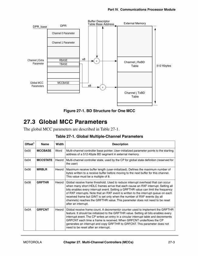
Part IV. Communications Processor Module
Figure 27-1. BD Structure for One MCC
27.3 Global MCC ParametersThe global MCC parameters are described in Table 27-1.
Table 27-1. Global Multiple-Channel Parameters
Offset1 Name Width Description
0x00 MCCBASE Word Multi-channel controller base pointer. User-initialized parameter points to the starting address of a 512-Kbyte BD segment in external memory.
0x04 MCCSTATE Hword Multi-channel controller state, used by the CP for global state deÞnition (reserved for the user)
0x06 MRBLR Hword Maximum receive buffer length (user-initialized). DeÞnes the maximum number of bytes written to a receive buffer before moving to the next buffer for this channel. This value must be a multiple of 8.
0x08 GRFTHR Hword Global receive frame threshold. Used to reduce interrupt overhead that can occur when many short HDLC frames arrive that each cause an RXF interrupt. Setting all bits enables every interrupt event. Setting a GRFTHR value can limit the frequency of RXF interrupts. Note that an RXF event is written to the interrupt queue on each received frame but GINT is set only when the number of RXF events (by all channels) reaches the GRFTHR value. This parameter does not need to be reset after an interrupt.
0x0A GRFCNT Hword Global receive frame count. A decrementor counter used to implement the GRFTHR feature. It should be initialized to the GRFTHR value. Setting all bits enables every interrupt event. The CP writes an entry in a circular interrupt table and decrements GRFCNT each time a frame is received. When GRFCNT underßows the CP generates an interrupt and copy GRFTHR to GRFCNT. This parameter does not need to be reset after an interrupt.
Channel j TxBD Table
Channel 0 Parameter
Channel 1 Parameter
Channel j Extra RBASETBASE
Global MCC MCCBASE
DPR
Buffer Descriptor
+
+
Channel j RxBD Table
External Memory
512 Kbytes
x8
x8
DPR_baseTable Base Address
Parameter
Parameters
MOTOROLA Chapter 27. Multi-Channel Controllers (MCCs) 27-3
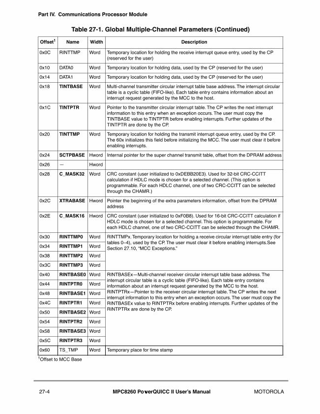
Part IV. Communications Processor Module
0x0C RINTTMP Word Temporary location for holding the receive interrupt queue entry, used by the CP (reserved for the user)
0x10 DATA0 Word Temporary location for holding data, used by the CP (reserved for the user)
0x14 DATA1 Word Temporary location for holding data, used by the CP (reserved for the user)
0x18 TINTBASE Word Multi-channel transmitter circular interrupt table base address. The interrupt circular table is a cyclic table (FIFO-like). Each table entry contains information about an interrupt request generated by the MCC to the host.
0x1C TINTPTR Word Pointer to the transmitter circular interrupt table. The CP writes the next interrupt information to this entry when an exception occurs. The user must copy the TINTBASE value to TINTPTR before enabling interrupts. Further updates of the TINTPTR are done by the CP.
0x20 TINTTMP Word Temporary location for holding the transmit interrupt queue entry, used by the CP. The 60x initializes this Þeld before initializing the MCC. The user must clear it before enabling interrupts.
0x24 SCTPBASE Hword Internal pointer for the super channel transmit table, offset from the DPRAM address
0x26 Ñ Hword
0x28 C_MASK32 Word CRC constant (user initialized to 0xDEBB20E3). Used for 32-bit CRC-CCITT calculation if HDLC mode is chosen for a selected channel. (This option is programmable. For each HDLC channel, one of two CRC-CCITT can be selected through the CHAMR.)
0x2C XTRABASE Hword Pointer the beginning of the extra parameters information, offset from the DPRAM address
0x2E C_MASK16 Hword CRC constant (user initialized to 0xF0B8). Used for 16-bit CRC-CCITT calculation if HDLC mode is chosen for a selected channel. This option is programmable. For each HDLC channel, one of two CRC-CCITT can be selected through the CHAMR.
0x30 RINTTMP0 Word RINTTMPx. Temporary location for holding a receive circular interrupt table entry (for tables 0Ð4), used by the CP. The user must clear it before enabling interrupts.See Section 27.10, ÒMCC Exceptions.Ó 0x34 RINTTMP1 Word
0x38 RINTTMP2 Word
0x3C RINTTMP3 Word
0x40 RINTBASE0 Word RINTBASExÑMulti-channel receiver circular interrupt table base address. The interrupt circular table is a cyclic table (FIFO-like). Each table entry contains information about an interrupt request generated by the MCC to the host. RINTPTRxÑPointer to the receiver circular interrupt table. The CP writes the next interrupt information to this entry when an exception occurs. The user must copy the RINTBASEx value to RINTPTRx before enabling interrupts. Further updates of the RINTPTRx are done by the CP.
0x44 RINTPTR0 Word
0x48 RINTBASE1 Word
0x4C RINTPTR1 Word
0x50 RINTBASE2 Word
0x54 RINTPTR2 Word
0x58 RINTBASE3 Word
0x5C RINTPTR3 Word
0x60 TS_TMP Word Temporary place for time stamp
1Offset to MCC Base
Table 27-1. Global Multiple-Channel Parameters (Continued)
Offset1 Name Width Description
27-4 MPC8260 PowerQUICC II UserÕs Manual MOTOROLA
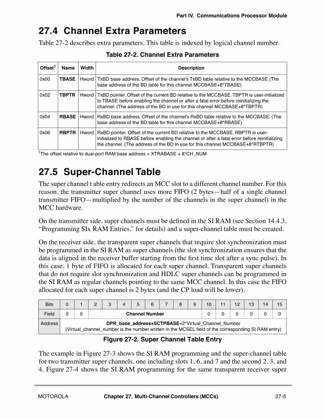
Part IV. Communications Processor Module
27.4 Channel Extra ParametersTable 27-2 describes extra parameters. This table is indexed by logical channel number.
27.5 Super-Channel Table The super channel t able entry redirects an MCC slot to a different channel number. For thisreason, the transmitter super channel uses more FIFO (2 bytesÑhalf of a single channeltransmitter FIFOÑmultiplied by the number of the channels in the super channel) in theMCC hardware.
On the transmitter side, super channels must be deÞned in the SI RAM (see Section 14.4.3,ÒProgramming SIx RAM Entries,Ó for details) and a super-channel table must be created.
On the receiver side, the transparent super channels that require slot synchronization mustbe programmed in the SI RAM as super channels (the slot synchronization ensures that thedata is aligned in the receiver buffer starting from the Þrst time slot after a sync pulse). Inthis case, 1 byte of FIFO is allocated for each super channel. Transparent super channelsthat do not require slot synchronization and HDLC super channels can be programmed inthe SI RAM as regular channels pointing to the same MCC channel. In this case the FIFOallocated for each super channel is 2 bytes (and the CP load will be lower).
The example in Figure 27-3 shows the SI RAM programming and the super-channel tablefor two transmitter super channels, one including slots 1, 6, and 7 and the second 2, 3, and4. Figure 27-4 shows the SI RAM programming for the same transparent receiver super
Table 27-2. Channel Extra Parameters
Offset1
1The offset relative to dual-port RAM base address + XTRABASE + 8*CH_NUM
Name Width Description
0x00 TBASE Hword TxBD base address. Offset of the channelÕs TxBD table relative to the MCCBASE (The base address of the BD table for this channel MCCBASE+8*TBASE)
0x02 TBPTR Hword TxBD pointer. Offset of the current BD relative to the MCCBASE. TBPTR is user-initialized to TBASE before enabling the channel or after a fatal error before reinitializing the channel. (The address of the BD in use for this channel MCCBASE+8*TBPTR)
0x04 RBASE Hword RxBD base address. Offset of the channelÕs RxBD table relative to the MCCBASE. (The base address of the BD table for this channel MCCBASE+8*RBASE)
0x06 RBPTR Hword RxBD pointer. Offset of the current BD relative to the MCCBASE. RBPTR is user-initialized to RBASE before enabling the channel or after a fatal error before reinitializing the channel. (The address of the BD in use for this channel MCCBASE+8*RTBPTR)
Bits 0 1 2 3 4 5 6 7 8 9 10 11 12 13 14 15
Field 0 0 Channel Number 0 0 0 0 0 0
Address DPR_base_address+SCTPBASE+2*Virtual_Channel_Number(Virtual_channel_number is the number written in the MCSEL Þeld of the corresponding SI RAM entry)
Figure 27-2. Super Channel Table Entry
MOTOROLA Chapter 27. Multi-Channel Controllers (MCCs) 27-5
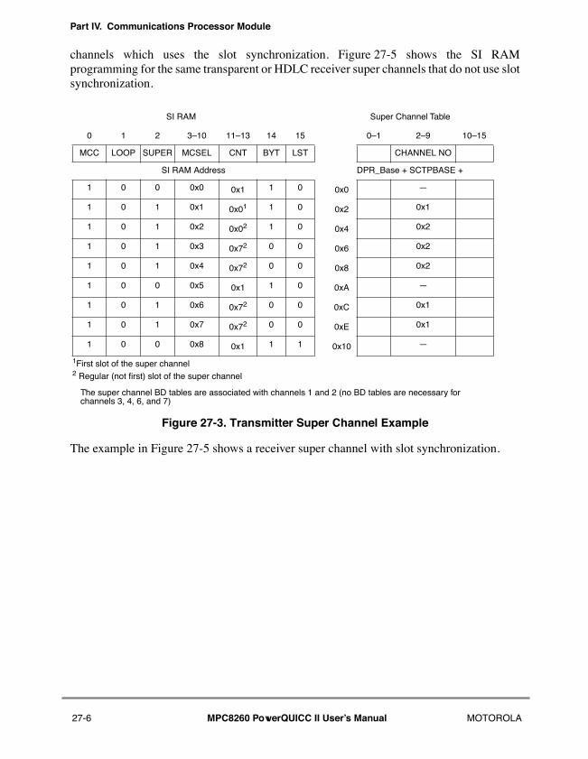
Part IV. Communications Processor Module
channels which uses the slot synchronization. Figure 27-5 shows the SI RAMprogramming for the same transparent or HDLC receiver super channels that do not use slotsynchronization.
Figure 27-3. Transmitter Super Channel Example
The example in Figure 27-5 shows a receiver super channel with slot synchronization.
0 1 2 3Ð10 11Ð13 14 15
MCC LOOP SUPER MCSEL CNT BYT LST
SI RAM Address
1 0 0 0x0 0x1 1 0
1 0 1 0x1 0x01
1First slot of the super channel
1 0
1 0 1 0x2 0x02 1 0
1 0 1 0x3 0x72
2 Regular (not Þrst) slot of the super channel
0 0
1 0 1 0x4 0x72 0 0
1 0 0 0x5 0x1 1 0
1 0 1 0x6 0x72 0 0
1 0 1 0x7 0x72 0 0
1 0 0 0x8 0x1 1 1
0Ð1 2Ð9 10Ð15
CHANNEL NO
DPR_Base + SCTPBASE +
0x0 Ñ
0x2 0x1
0x4 0x2
0x6 0x2
0x8 0x2
0xA Ñ
0xC 0x1
0xE 0x1
0x10 Ñ
.The super channel BD tables are associated with channels 1 and 2 (no BD tables are necessary for
SI RAM Super Channel Table
channels 3, 4, 6, and 7)
27-6 MPC8260 PowerQUICC II UserÕs Manual MOTOROLA
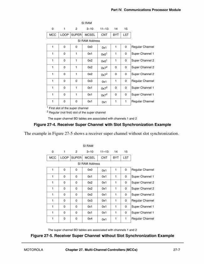
Part IV. Communications Processor Module
Figure 27-4. Receiver Super Channel with Slot Synchronization Example
The example in Figure 27-5 shows a receiver super channel without slot synchronization.
Figure 27-5. Receiver Super Channel without Slot Synchronization Example
0 1 2 3Ð10 11Ð13 14 15
MCC LOOP SUPER MCSEL CNT BYT LST
SI RAM Address
1 0 0 0x0 0x1 1 0 Regular Channel
1 0 1 0x1 0x01
1 First slot of the super channel
1 0 Super Channel 1
1 0 1 0x2 0x01 1 0 Super Channel 2
1 0 1 0x2 0x72
2 Regular (not Þrst) slot of the super channel
0 0 Super Channel 2
1 0 1 0x2 0x72 0 0 Super Channel 2
1 0 0 0x3 0x1 1 0 Regular Channel
1 0 1 0x1 0x72 0 0 Super Channel 1
1 0 1 0x1 0x72 0 0 Super Channel 1
1 0 0 0x1 0x1 1 1 Regular Channel
The super channel BD tables are associated with channels 1 and 2
SI RAM
0 1 2 3Ð10 11Ð13 14 15
MCC LOOP SUPER MCSEL CNT BYT LST
SI RAM Address
1 0 0 0x0 0x1 1 0 Regular Channel
1 0 0 0x1 0x1 1 0 Super Channel 1
1 0 0 0x2 0x1 1 0 Super Channel 2
1 0 0 0x2 0x1 1 0 Super Channel 2
1 0 0 0x2 0x1 1 0 Super Channel 2
1 0 0 0x3 0x1 1 0 Regular Channel
1 0 0 0x1 0x1 1 0 Super Channel 1
1 0 0 0x1 0x1 1 0 Super Channel 1
1 0 0 0x4 0x1 1 1 Regular Channel
The super channel BD tables are associated with channels 1 and 2
SI RAM
MOTOROLA Chapter 27. Multi-Channel Controllers (MCCs) 27-7
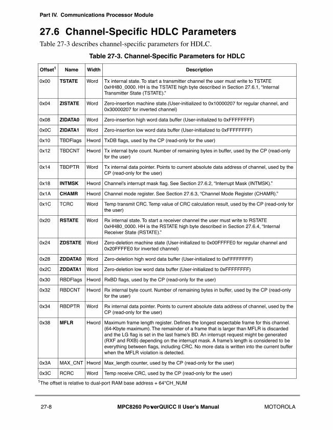
Part IV. Communications Processor Module
27.6 Channel-SpeciÞc HDLC ParametersTable 27-3 describes channel-speciÞc parameters for HDLC.
Table 27-3. Channel-Specific Parameters for HDLC
Offset1
1The offset is relative to dual-port RAM base address + 64*CH_NUM
Name Width Description
0x00 TSTATE Word Tx internal state. To start a transmitter channel the user must write to TSTATE 0xHH80_0000. HH is the TSTATE high byte described in Section 27.6.1, ÒInternal Transmitter State (TSTATE).Ó
0x04 ZISTATE Word Zero-insertion machine state.(User-initialized to 0x10000207 for regular channel, and 0x30000207 for inverted channel)
0x08 ZIDATA0 Word Zero-insertion high word data buffer (User-initialized to 0xFFFFFFFF)
0x0C ZIDATA1 Word Zero-insertion low word data buffer (User-initialized to 0xFFFFFFFF)
0x10 TBDFlags Hword TxDB ßags, used by the CP (read-only for the user)
0x12 TBDCNT Hword Tx internal byte count. Number of remaining bytes in buffer, used by the CP (read-only for the user)
0x14 TBDPTR Word Tx internal data pointer. Points to current absolute data address of channel, used by the CP (read-only for the user)
0x18 INTMSK Hword ChannelÕs interrupt mask ßag. See Section 27.6.2, ÒInterrupt Mask (INTMSK).Ó
0x1A CHAMR Hword Channel mode register. See Section 27.6.3, ÒChannel Mode Register (CHAMR).Ó
0x1C TCRC Word Temp transmit CRC. Temp value of CRC calculation result, used by the CP (read-only for the user)
0x20 RSTATE Word Rx internal state. To start a receiver channel the user must write to RSTATE 0xHH80_0000. HH is the RSTATE high byte described in Section 27.6.4, ÒInternal Receiver State (RSTATE).Ó
0x24 ZDSTATE Word Zero-deletion machine state (User-initialized to 0x00FFFFE0 for regular channel and 0x20FFFFE0 for inverted channel)
0x28 ZDDATA0 Word Zero-deletion high word data buffer (User-initialized to 0xFFFFFFFF)
0x2C ZDDATA1 Word Zero-deletion low word data buffer (User-initialized to 0xFFFFFFFF)
0x30 RBDFlags Hword RxBD ßags, used by the CP (read-only for the user)
0x32 RBDCNT Hword Rx internal byte count. Number of remaining bytes in buffer, used by the CP (read-only for the user)
0x34 RBDPTR Word Rx internal data pointer. Points to current absolute data address of channel, used by the CP (read-only for the user)
0x38 MFLR Hword Maximum frame length register. DeÞnes the longest expectable frame for this channel. (64-Kbyte maximum). The remainder of a frame that is larger than MFLR is discarded and the LG ßag is set in the last frameÕs BD. An interrupt request might be generated (RXF and RXB) depending on the interrupt mask. A frameÕs length is considered to be everything between ßags, including CRC. No more data is written into the current buffer when the MFLR violation is detected.
0x3A MAX_CNT Hword Max_length counter, used by the CP (read-only for the user)
0x3C RCRC Word Temp receive CRC, used by the CP (read-only for the user)
27-8 MPC8260 PowerQUICC II UserÕs Manual MOTOROLA
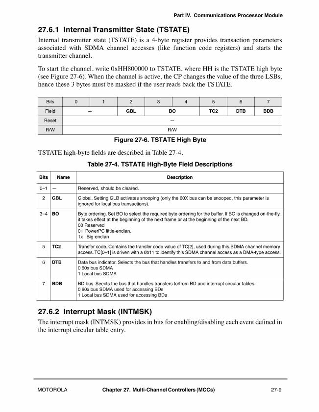
Part IV. Communications Processor Module
27.6.1 Internal Transmitter State (TSTATE)Internal transmitter state (TSTATE) is a 4-byte register provides transaction parametersassociated with SDMA channel accesses (like function code registers) and starts thetransmitter channel.
To start the channel, write 0xHH800000 to TSTATE, where HH is the TSTATE high byte(see Figure 27-6). When the channel is active, the CP changes the value of the three LSBs,hence these 3 bytes must be masked if the user reads back the TSTATE.
TSTATE high-byte Þelds are described in Table 27-4.
27.6.2 Interrupt Mask (INTMSK)The interrupt mask (INTMSK) provides in bits for enabling/disabling each event deÞned inthe interrupt circular table entry.
Bits 0 1 2 3 4 5 6 7
Field Ñ GBL BO TC2 DTB BDB
Reset Ñ
R/W R/W
Figure 27-6. TSTATE High Byte
Table 27-4. TSTATE High-Byte Field Descriptions
Bits Name Description
0Ð1 Ñ Reserved, should be cleared.
2 GBL Global. Setting GLB activates snooping (only the 60X bus can be snooped, this parameter is ignored for local bus transactions).
3Ð4 BO Byte ordering. Set BO to select the required byte ordering for the buffer. If BO is changed on-the-ßy, it takes effect at the beginning of the next frame or at the beginning of the next BD. 00 Reserved01 PowerPC little-endian. 1x Big-endian
5 TC2 Transfer code. Contains the transfer code value of TC[2], used during this SDMA channel memory access. TC[0Ð1] is driven with a 0b11 to identify this SDMA channel access as a DMA-type access.
6 DTB Data bus indicator. Selects the bus that handles transfers to and from data buffers.0 60x bus SDMA 1 Local bus SDMA
7 BDB BD bus. Seects the bus that handles transfers to/from BD and interrupt circular tables.0 60x bus SDMA used for accessing BDs1 Local bus SDMA used for accessing BDs
MOTOROLA Chapter 27. Multi-Channel Controllers (MCCs) 27-9
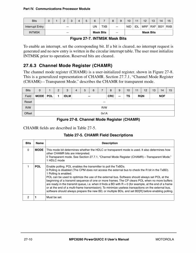
Part IV. Communications Processor Module
To enable an interrupt, set the corresponding bit. If a bit is cleared, no interrupt request isgenerated and no new entry is written in the circular interrupt table. The user must initializeINTMSK prior to operation. Reserved bits are cleared.
27.6.3 Channel Mode Register (CHAMR)The channel mode register (CHAMR) is a user-initialized register, shown in Figure 27-8.This is a generalized representation of CHAMR. Section 27.7.1, ÒChannel Mode Register(CHAMR)ÑTransparent Mode,Ó describes the CHAMR for transparent mode.
CHAMR Þelds are described in Table 27-5.
Bits 0 1 2 3 4 5 6 7 8 9 10 11 12 13 14 15
Interrupt Entry Ñ UN TXB Ñ NID IDL MRF RXF BSY RXB
INTMSK Ñ Mask Bits Ñ Mask Bits
Figure 27-7. INTMSK Mask Bits
Bits 0 1 2 3 4 5 6 7 8 9 10 11 12 13 14 15
Field MODE POL 1 IDLM Ñ CRC Ñ TS RQN NOF
Reset Ñ
R/W R/W
Offset 0x1A
Figure 27-8. Channel Mode Register (CHAMR)
Table 27-5. CHAMR Field Descriptions
Bits Name Description
0 MODE This mode bit determines whether the HDLC or transparent mode is used. It also determines how other CHAMR bits are interpreted. 0 Transparent mode. See Section 27.7.1, ÒChannel Mode Register (CHAMR)ÑTransparent Mode.Ó1 HDLC mode
1 POL Enable polling. POL enables the transmitter to poll the TxBDs. 0 Polling is disabled (The CPM does not access the external bus to check the R bit in the TxBD).1 Polling is enabled. POL can be used to optimize the use of the external bus. Software should always set POL at the beginning of a transmit sequence of one or more frames. The CP clears POL when no more buffers are ready in the transmit queue, i.e. when it Þnds a BD with R = 0 (for example, at the end of a frame or at the end of a multi-frame transmission). To minimize useless transactions on the external bus, software should always prepare the new BD, or multiple BDs, and set BD[R] before enabling polling.
2 1 Must be set.
27-10 MPC8260 PowerQUICC II UserÕs Manual MOTOROLA
Part IV. Communications Processor Module
27.6.4 Internal Receiver State (RSTATE)Internal receiver state (RSTATE) is a 4-byte register that provides transaction parametersassociated with SDMA channel accesses (like function code registers) and starts thereceiver channel.
To start the channel the user must write 0xHH800000 to RSTATE, where HH is theRSTATE high byte (see Figure 27-9). When the channel is active the CP changes the valueof the 3 LSBs, hence these 3 bytes must be masked if the user reads back the RSTATE.
3 IDLM Idle mode. 0 No idle patterns are sent between frames. After sending NOF+1 ßags, the transmitter starts
sending the data of the frame. If the transmission is between frames and the frame buffers are not ready, the transmitter sends ßags until it can start transmitting the data.
1 At least one idle pattern is sent between adjacent frames. The NOF value shall be no smaller than the PAD setting, see TxBD. If NOF = 0, this is identical to ßag sharing in HDLC. Mode ßags precede the actual data. When IDLM = 1, at least one idle pattern is sent between adjacent frames. If the transmission is between frames and the frame buffer is not ready, the transmitter sends idle characters. When data is ready, the NOF+1 ßags are sent followed by the data frame.
If IDLE mode is selected and NOF = 1, the following sequence is sent:......init value, FF, FF, ßag, ßag, data, ........
The init value before the idle will be ones.
4Ð7 Ñ These bits must be cleared.
8 CRC Selects the type of CRC when HDLC channel mode is used. 0 16-bit CCITT-CRC 1 32-bit CCITT-CRC
9 Ñ This bit must be cleared.
10 TS Receive time stamp. If this bit is set a 4 byte time stamp is written at the beginning of every data buffer that the BD points to.If this bit is set the data buffer must start from an address equal to 8*n-4 (n is any integer larger than 0).
11Ð12 RQN Receive queue number. SpeciÞes the receive interrupt queue number.00 Queue number 0.01 Queue number 1.10 Queue number 2.11 Queue number 3.
13Ð15 NOF Number of ßags. NOF deÞnes the minimum number of ßags before frames:000 At least 1 ßag001 At least 2 ßags....111 At least 8 ßags
Table 27-5. CHAMR Field Descriptions (Continued)
Bits Name Description
MOTOROLA Chapter 27. Multi-Channel Controllers (MCCs) 27-11
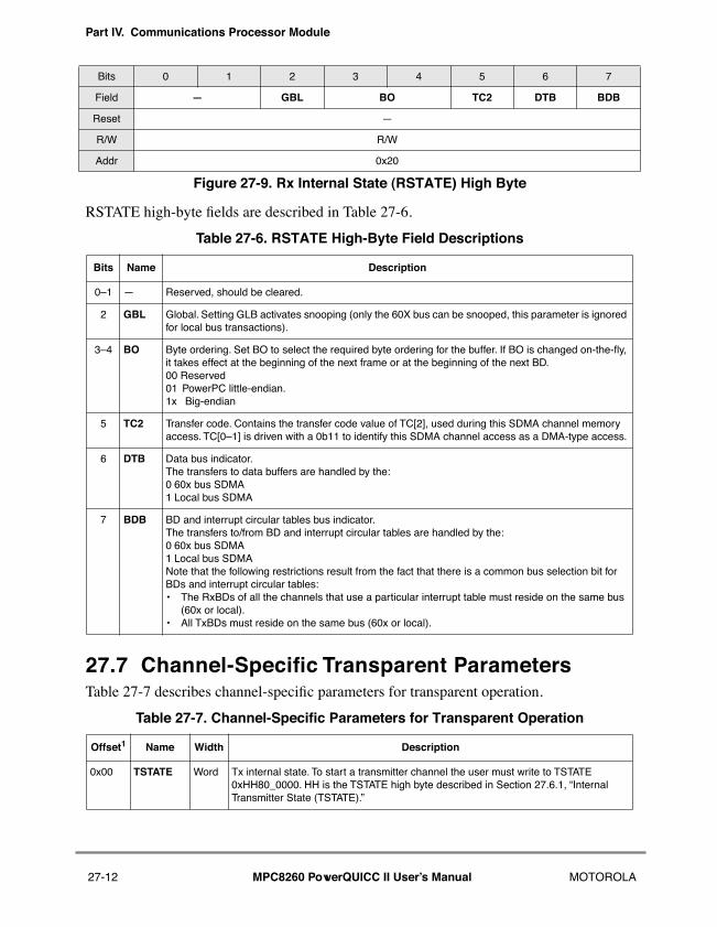
Part IV. Communications Processor Module
RSTATE high-byte Þelds are described in Table 27-6.
27.7 Channel-SpeciÞc Transparent ParametersTable 27-7 describes channel-speciÞc parameters for transparent operation.
Bits 0 1 2 3 4 5 6 7
Field Ñ GBL BO TC2 DTB BDB
Reset Ñ
R/W R/W
Addr 0x20
Figure 27-9. Rx Internal State (RSTATE) High Byte
Table 27-6. RSTATE High-Byte Field Descriptions
Bits Name Description
0Ð1 Ñ Reserved, should be cleared.
2 GBL Global. Setting GLB activates snooping (only the 60X bus can be snooped, this parameter is ignored for local bus transactions).
3Ð4 BO Byte ordering. Set BO to select the required byte ordering for the buffer. If BO is changed on-the-ßy, it takes effect at the beginning of the next frame or at the beginning of the next BD. 00 Reserved01 PowerPC little-endian. 1x Big-endian
5 TC2 Transfer code. Contains the transfer code value of TC[2], used during this SDMA channel memory access. TC[0Ð1] is driven with a 0b11 to identify this SDMA channel access as a DMA-type access.
6 DTB Data bus indicator. The transfers to data buffers are handled by the:0 60x bus SDMA 1 Local bus SDMA
7 BDB BD and interrupt circular tables bus indicator.The transfers to/from BD and interrupt circular tables are handled by the:0 60x bus SDMA 1 Local bus SDMA Note that the following restrictions result from the fact that there is a common bus selection bit for BDs and interrupt circular tables:¥ The RxBDs of all the channels that use a particular interrupt table must reside on the same bus
(60x or local).¥ All TxBDs must reside on the same bus (60x or local).
Table 27-7. Channel-Specific Parameters for Transparent Operation
Offset1 Name Width Description
0x00 TSTATE Word Tx internal state. To start a transmitter channel the user must write to TSTATE 0xHH80_0000. HH is the TSTATE high byte described in Section 27.6.1, ÒInternal Transmitter State (TSTATE).Ó
27-12 MPC8260 PowerQUICC II UserÕs Manual MOTOROLA
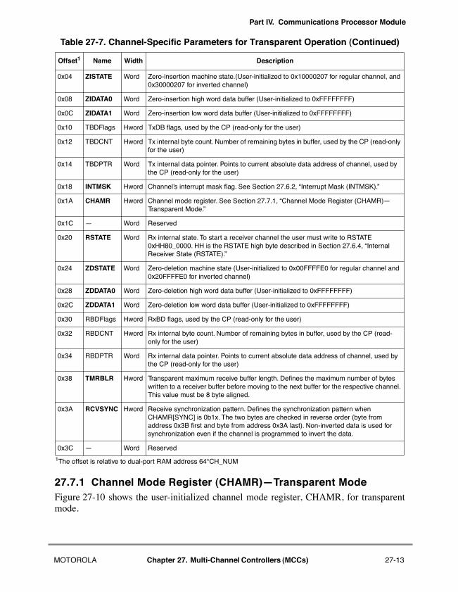
Part IV. Communications Processor Module
27.7.1 Channel Mode Register (CHAMR)ÑTransparent ModeFigure 27-10 shows the user-initialized channel mode register, CHAMR, for transparentmode.
0x04 ZISTATE Word Zero-insertion machine state.(User-initialized to 0x10000207 for regular channel, and 0x30000207 for inverted channel)
0x08 ZIDATA0 Word Zero-insertion high word data buffer (User-initialized to 0xFFFFFFFF)
0x0C ZIDATA1 Word Zero-insertion low word data buffer (User-initialized to 0xFFFFFFFF)
0x10 TBDFlags Hword TxDB ßags, used by the CP (read-only for the user)
0x12 TBDCNT Hword Tx internal byte count. Number of remaining bytes in buffer, used by the CP (read-only for the user)
0x14 TBDPTR Word Tx internal data pointer. Points to current absolute data address of channel, used by the CP (read-only for the user)
0x18 INTMSK Hword ChannelÕs interrupt mask ßag. See Section 27.6.2, ÒInterrupt Mask (INTMSK).Ó
0x1A CHAMR Hword Channel mode register. See Section 27.7.1, ÒChannel Mode Register (CHAMR)ÑTransparent Mode.Ó
0x1C Ñ Word Reserved
0x20 RSTATE Word Rx internal state. To start a receiver channel the user must write to RSTATE 0xHH80_0000. HH is the RSTATE high byte described in Section 27.6.4, ÒInternal Receiver State (RSTATE).Ó
0x24 ZDSTATE Word Zero-deletion machine state (User-initialized to 0x00FFFFE0 for regular channel and 0x20FFFFE0 for inverted channel)
0x28 ZDDATA0 Word Zero-deletion high word data buffer (User-initialized to 0xFFFFFFFF)
0x2C ZDDATA1 Word Zero-deletion low word data buffer (User-initialized to 0xFFFFFFFF)
0x30 RBDFlags Hword RxBD ßags, used by the CP (read-only for the user)
0x32 RBDCNT Hword Rx internal byte count. Number of remaining bytes in buffer, used by the CP (read-only for the user)
0x34 RBDPTR Word Rx internal data pointer. Points to current absolute data address of channel, used by the CP (read-only for the user)
0x38 TMRBLR Hword Transparent maximum receive buffer length. DeÞnes the maximum number of bytes written to a receiver buffer before moving to the next buffer for the respective channel. This value must be 8 byte aligned.
0x3A RCVSYNC Hword Receive synchronization pattern. DeÞnes the synchronization pattern when CHAMR[SYNC] is 0b1x. The two bytes are checked in reverse order (byte from address 0x3B Þrst and byte from address 0x3A last). Non-inverted data is used for synchronization even if the channel is programmed to invert the data.
0x3C Ñ Word Reserved
1The offset is relative to dual-port RAM address 64*CH_NUM
Table 27-7. Channel-Specific Parameters for Transparent Operation (Continued)
Offset1 Name Width Description
MOTOROLA Chapter 27. Multi-Channel Controllers (MCCs) 27-13
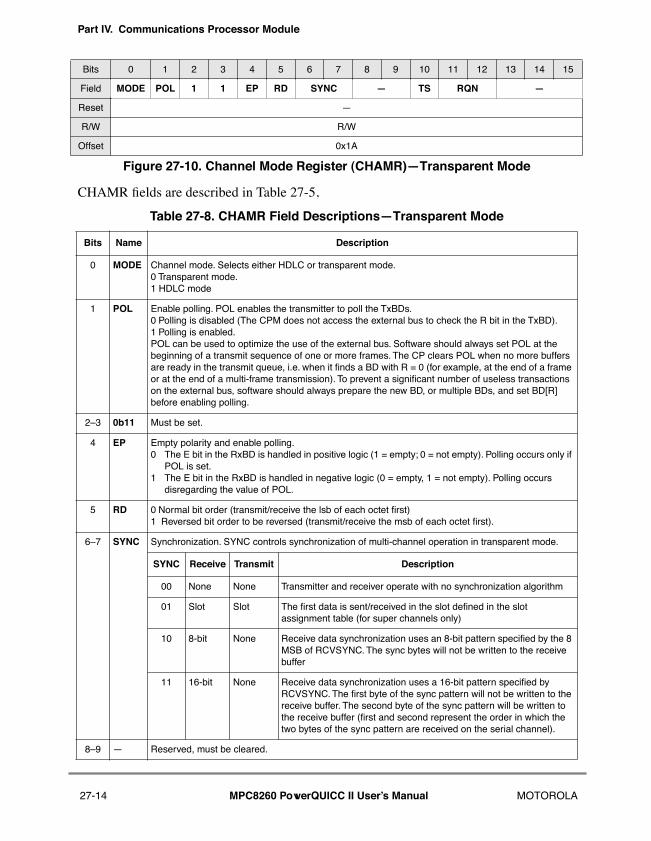
Part IV. Communications Processor Module
CHAMR Þelds are described in Table 27-5,
Bits 0 1 2 3 4 5 6 7 8 9 10 11 12 13 14 15
Field MODE POL 1 1 EP RD SYNC Ñ TS RQN Ñ
Reset Ñ
R/W R/W
Offset 0x1A
Figure 27-10. Channel Mode Register (CHAMR)ÑTransparent Mode
Table 27-8. CHAMR Field DescriptionsÑTransparent Mode
Bits Name Description
0 MODE Channel mode. Selects either HDLC or transparent mode.0 Transparent mode.1 HDLC mode
1 POL Enable polling. POL enables the transmitter to poll the TxBDs. 0 Polling is disabled (The CPM does not access the external bus to check the R bit in the TxBD).1 Polling is enabled. POL can be used to optimize the use of the external bus. Software should always set POL at the beginning of a transmit sequence of one or more frames. The CP clears POL when no more buffers are ready in the transmit queue, i.e. when it Þnds a BD with R = 0 (for example, at the end of a frame or at the end of a multi-frame transmission). To prevent a signiÞcant number of useless transactions on the external bus, software should always prepare the new BD, or multiple BDs, and set BD[R] before enabling polling.
2Ð3 0b11 Must be set.
4 EP Empty polarity and enable polling.0 The E bit in the RxBD is handled in positive logic (1 = empty; 0 = not empty). Polling occurs only if
POL is set.1 The E bit in the RxBD is handled in negative logic (0 = empty, 1 = not empty). Polling occurs
disregarding the value of POL.
5 RD 0 Normal bit order (transmit/receive the lsb of each octet Þrst)1 Reversed bit order to be reversed (transmit/receive the msb of each octet Þrst).
6Ð7 SYNC Synchronization. SYNC controls synchronization of multi-channel operation in transparent mode.
SYNC Receive Transmit Description
00 None None Transmitter and receiver operate with no synchronization algorithm
01 Slot Slot The Þrst data is sent/received in the slot deÞned in the slot assignment table (for super channels only)
10 8-bit None Receive data synchronization uses an 8-bit pattern speciÞed by the 8 MSB of RCVSYNC. The sync bytes will not be written to the receive buffer
11 16-bit None Receive data synchronization uses a 16-bit pattern speciÞed by RCVSYNC. The Þrst byte of the sync pattern will not be written to the receive buffer. The second byte of the sync pattern will be written to the receive buffer (Þrst and second represent the order in which the two bytes of the sync pattern are received on the serial channel).
8Ð9 Ñ Reserved, must be cleared.
27-14 MPC8260 PowerQUICC II UserÕs Manual MOTOROLA
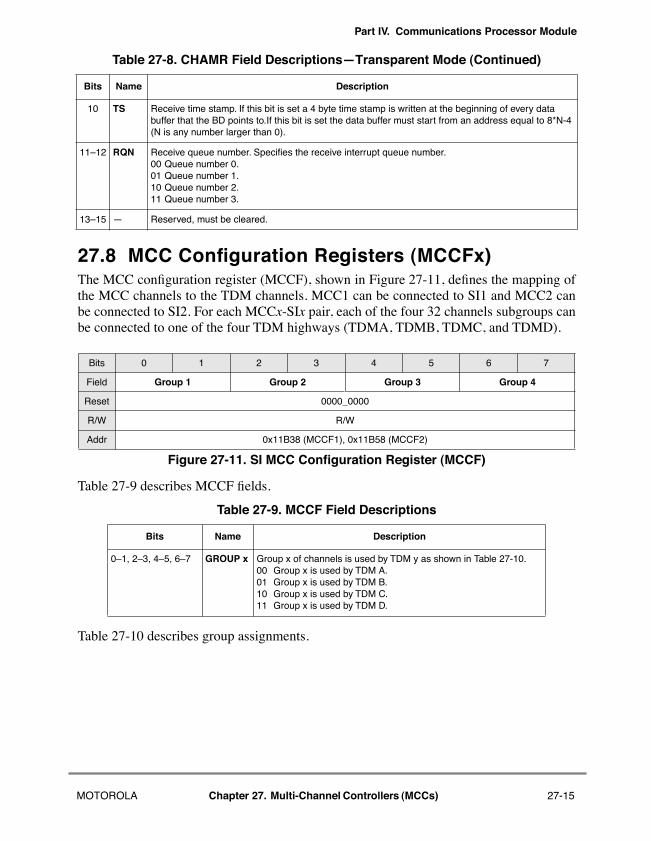
Part IV. Communications Processor Module
27.8 MCC ConÞguration Registers (MCCFx)The MCC conÞguration register (MCCF), shown in Figure 27-11, deÞnes the mapping ofthe MCC channels to the TDM channels. MCC1 can be connected to SI1 and MCC2 canbe connected to SI2. For each MCCx-SIx pair, each of the four 32 channels subgroups canbe connected to one of the four TDM highways (TDMA, TDMB, TDMC, and TDMD).
Table 27-9 describes MCCF Þelds.
Table 27-10 describes group assignments.
10 TS Receive time stamp. If this bit is set a 4 byte time stamp is written at the beginning of every data buffer that the BD points to.If this bit is set the data buffer must start from an address equal to 8*N-4 (N is any number larger than 0).
11Ð12 RQN Receive queue number. SpeciÞes the receive interrupt queue number.00 Queue number 0.01 Queue number 1.10 Queue number 2.11 Queue number 3.
13Ð15 Ñ Reserved, must be cleared.
Bits 0 1 2 3 4 5 6 7
Field Group 1 Group 2 Group 3 Group 4
Reset 0000_0000
R/W R/W
Addr 0x11B38 (MCCF1), 0x11B58 (MCCF2)
Figure 27-11. SI MCC Configuration Register (MCCF)
Table 27-9. MCCF Field Descriptions
Bits Name Description
0Ð1, 2Ð3, 4Ð5, 6Ð7 GROUP x Group x of channels is used by TDM y as shown in Table 27-10.00 Group x is used by TDM A.01 Group x is used by TDM B.10 Group x is used by TDM C.11 Group x is used by TDM D.
Table 27-8. CHAMR Field DescriptionsÑTransparent Mode (Continued)
Bits Name Description
MOTOROLA Chapter 27. Multi-Channel Controllers (MCCs) 27-15
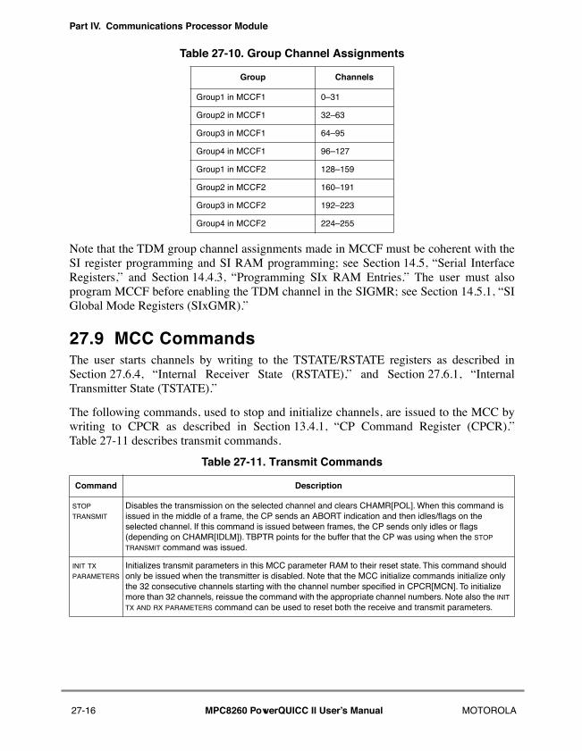
Part IV. Communications Processor Module
Note that the TDM group channel assignments made in MCCF must be coherent with theSI register programming and SI RAM programming; see Section 14.5, ÒSerial InterfaceRegisters,Ó and Section 14.4.3, ÒProgramming SIx RAM Entries.Ó The user must alsoprogram MCCF before enabling the TDM channel in the SIGMR; see Section 14.5.1, ÒSIGlobal Mode Registers (SIxGMR).Ó
27.9 MCC CommandsThe user starts channels by writing to the TSTATE/RSTATE registers as described inSection 27.6.4, ÒInternal Receiver State (RSTATE),Ó and Section 27.6.1, ÒInternalTransmitter State (TSTATE).Ó
The following commands, used to stop and initialize channels, are issued to the MCC bywriting to CPCR as described in Section 13.4.1, ÒCP Command Register (CPCR).ÓTable 27-11 describes transmit commands.
Table 27-10. Group Channel Assignments
Group Channels
Group1 in MCCF1 0Ð31
Group2 in MCCF1 32Ð63
Group3 in MCCF1 64Ð95
Group4 in MCCF1 96Ð127
Group1 in MCCF2 128Ð159
Group2 in MCCF2 160Ð191
Group3 in MCCF2 192Ð223
Group4 in MCCF2 224Ð255
Table 27-11. Transmit Commands
Command Description
STOP TRANSMIT
Disables the transmission on the selected channel and clears CHAMR[POL]. When this command is issued in the middle of a frame, the CP sends an ABORT indication and then idles/ßags on the selected channel. If this command is issued between frames, the CP sends only idles or ßags (depending on CHAMR[IDLM]). TBPTR points for the buffer that the CP was using when the STOP TRANSMIT command was issued.
INIT TX PARAMETERS
Initializes transmit parameters in this MCC parameter RAM to their reset state. This command should only be issued when the transmitter is disabled. Note that the MCC initialize commands initialize only the 32 consecutive channels starting with the channel number speciÞed in CPCR[MCN]. To initialize more than 32 channels, reissue the command with the appropriate channel numbers. Note also the INIT TX AND RX PARAMETERS command can be used to reset both the receive and transmit parameters.
27-16 MPC8260 PowerQUICC II UserÕs Manual MOTOROLA
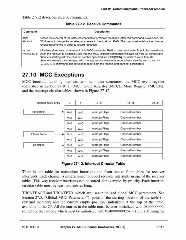
Part IV. Communications Processor Module
Table 27-12 describes receive commands.
27.10 MCC ExceptionsMCC interrupt handling involves two main data structures, the MCC event register(described in Section 27.10.1, ÒMCC Event Register (MCCE)/Mask Register (MCCM))and the interrupt circular tables, shown in Figure 27-12.
Figure 27-12. Interrupt Circular Table
There is one table for transmitter interrupts and from one to four tables for receiverinterrupts. Each channel is programmed to report receiver interrupts in one of the receivertables. This way receiver interrupts can be sorted, for example, by priority. Each interruptcircular table must be least two entries long.
T/RINTBASE and T/RINTPTR, which are user-initialized global MCC parameters (SeeSection 27.3, ÒGlobal MCC ParametersÓ), point to the starting location of the table (inexternal memory) and the current empty position (initialized at the top of the table)available to the CP. All the entries in the table must be user-initialized with 0x00000000,except for the last one which must be initialized with 0x40000000 (W = 1, thus deÞning the
Table 27-12. Receive Commands
Command Description
STOP RECEIVE
Forces the receiver of the selected channel to terminate reception. After this command is executed, the CP does not change the receive parameters in the dual-port RAM. The user must initialize the channel receive parameters in order to restart reception.
INIT RX PARAMETERS
Initializes all receive parameters in this MCC parameter RAM to their reset state. Should be issued only when the receiver is disabled. Note that the MCC initialize commands initialize only the 32 consecutive channels starting with the channel number speciÞed in CPCR[MCN]. To initialize more than 32 channels, reissue the command with the appropriate channel numbers. Note also the INIT TX AND RX PARAMETERS command can be used to reset both the receive and transmit parameters.
V=0 W=0 Interrupt Flags Channel NumberT/RINTBASE
V=0 W=0 Interrupt Flags Channel Number
V=0 W=0 Interrupt Flags Channel Number
V=0 W=0 Interrupt Flags Channel Number
V=1 W=0 Interrupt Flags Channel Number
V=1 W=0 Interrupt Flags Channel Number
V=0 W=0 Interrupt Flags Channel Number
V=0 W=0 Interrupt Flags Channel Number
V=0 W=1 Interrupt Flags Channel Number
T/RINTPTR
Software Pointer
0 1 2Ð17 18Ð25 26Ð31Interrupt Table Entry
MOTOROLA Chapter 27. Multi-Channel Controllers (MCCs) 27-17
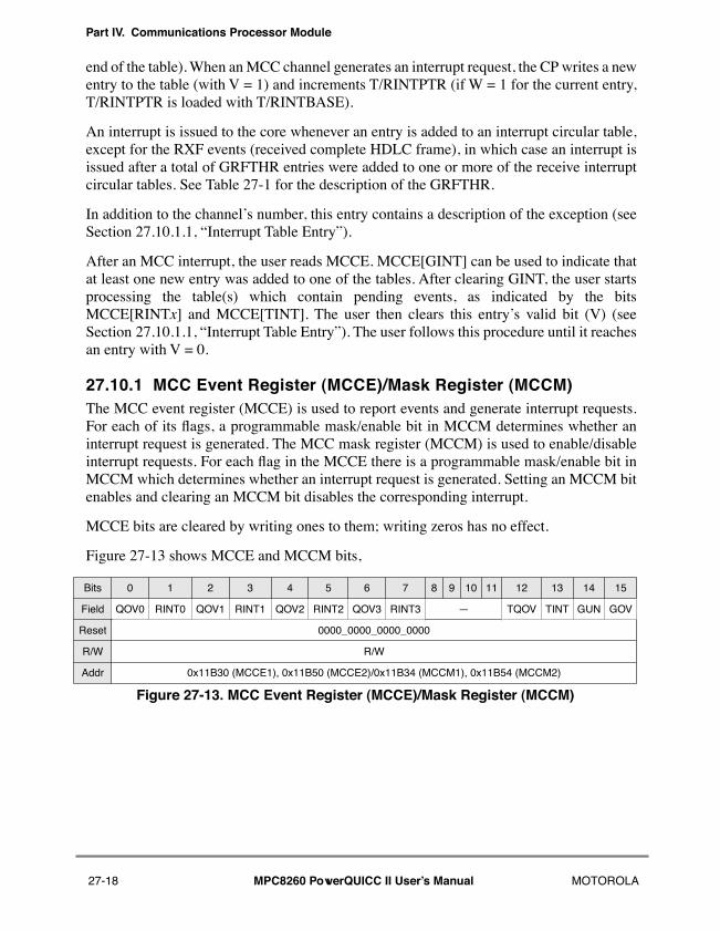
Part IV. Communications Processor Module
end of the table). When an MCC channel generates an interrupt request, the CP writes a newentry to the table (with V = 1) and increments T/RINTPTR (if W = 1 for the current entry,T/RINTPTR is loaded with T/RINTBASE).
An interrupt is issued to the core whenever an entry is added to an interrupt circular table,except for the RXF events (received complete HDLC frame), in which case an interrupt isissued after a total of GRFTHR entries were added to one or more of the receive interruptcircular tables. See Table 27-1 for the description of the GRFTHR.
In addition to the channelÕs number, this entry contains a description of the exception (seeSection 27.10.1.1, ÒInterrupt Table EntryÓ).
After an MCC interrupt, the user reads MCCE. MCCE[GINT] can be used to indicate thatat least one new entry was added to one of the tables. After clearing GINT, the user startsprocessing the table(s) which contain pending events, as indicated by the bitsMCCE[RINTx] and MCCE[TINT]. The user then clears this entryÕs valid bit (V) (seeSection 27.10.1.1, ÒInterrupt Table EntryÓ). The user follows this procedure until it reachesan entry with V = 0.
27.10.1 MCC Event Register (MCCE)/Mask Register (MCCM)The MCC event register (MCCE) is used to report events and generate interrupt requests.For each of its ßags, a programmable mask/enable bit in MCCM determines whether aninterrupt request is generated. The MCC mask register (MCCM) is used to enable/disableinterrupt requests. For each ßag in the MCCE there is a programmable mask/enable bit inMCCM which determines whether an interrupt request is generated. Setting an MCCM bitenables and clearing an MCCM bit disables the corresponding interrupt.
MCCE bits are cleared by writing ones to them; writing zeros has no effect.
Figure 27-13 shows MCCE and MCCM bits,
Bits 0 1 2 3 4 5 6 7 8 9 10 11 12 13 14 15
Field QOV0 RINT0 QOV1 RINT1 QOV2 RINT2 QOV3 RINT3 Ñ TQOV TINT GUN GOV
Reset 0000_0000_0000_0000
R/W R/W
Addr 0x11B30 (MCCE1), 0x11B50 (MCCE2)/0x11B34 (MCCM1), 0x11B54 (MCCM2)
Figure 27-13. MCC Event Register (MCCE)/Mask Register (MCCM)
27-18 MPC8260 PowerQUICC II UserÕs Manual MOTOROLA
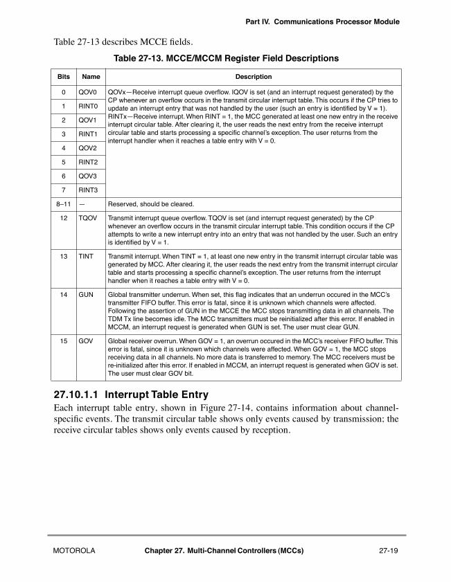
Part IV. Communications Processor Module
Table 27-13 describes MCCE Þelds.
27.10.1.1 Interrupt Table EntryEach interrupt table entry, shown in Figure 27-14, contains information about channel-speciÞc events. The transmit circular table shows only events caused by transmission; thereceive circular tables shows only events caused by reception.
Table 27-13. MCCE/MCCM Register Field Descriptions
Bits Name Description
0 QOV0 QOVxÑReceive interrupt queue overßow. IQOV is set (and an interrupt request generated) by the CP whenever an overßow occurs in the transmit circular interrupt table. This occurs if the CP tries to update an interrupt entry that was not handled by the user (such an entry is identiÞed by V = 1).RINTxÑReceive interrupt. When RINT = 1, the MCC generated at least one new entry in the receive interrupt circular table. After clearing it, the user reads the next entry from the receive interrupt circular table and starts processing a speciÞc channelÕs exception. The user returns from the interrupt handler when it reaches a table entry with V = 0.
1 RINT0
2 QOV1
3 RINT1
4 QOV2
5 RINT2
6 QOV3
7 RINT3
8Ð11 Ñ Reserved, should be cleared.
12 TQOV Transmit interrupt queue overßow. TQOV is set (and interrupt request generated) by the CP whenever an overßow occurs in the transmit circular interrupt table. This condition occurs if the CP attempts to write a new interrupt entry into an entry that was not handled by the user. Such an entry is identiÞed by V = 1.
13 TINT Transmit interrupt. When TINT = 1, at least one new entry in the transmit interrupt circular table was generated by MCC. After clearing it, the user reads the next entry from the transmit interrupt circular table and starts processing a speciÞc channelÕs exception. The user returns from the interrupt handler when it reaches a table entry with V = 0.
14 GUN Global transmitter underrun. When set, this ßag indicates that an underrun occured in the MCCÕs transmitter FIFO buffer. This error is fatal, since it is unknown which channels were affected. Following the assertion of GUN in the MCCE the MCC stops transmitting data in all channels. The TDM Tx line becomes idle. The MCC transmitters must be reinitialized after this error. If enabled in MCCM, an interrupt request is generated when GUN is set. The user must clear GUN.
15 GOV Global receiver overrun. When GOV = 1, an overrun occured in the MCCÕs receiver FIFO buffer. This error is fatal, since it is unknown which channels were affected. When GOV = 1, the MCC stops receiving data in all channels. No more data is transferred to memory. The MCC receivers must be re-initialized after this error. If enabled in MCCM, an interrupt request is generated when GOV is set. The user must clear GOV bit.
MOTOROLA Chapter 27. Multi-Channel Controllers (MCCs) 27-19
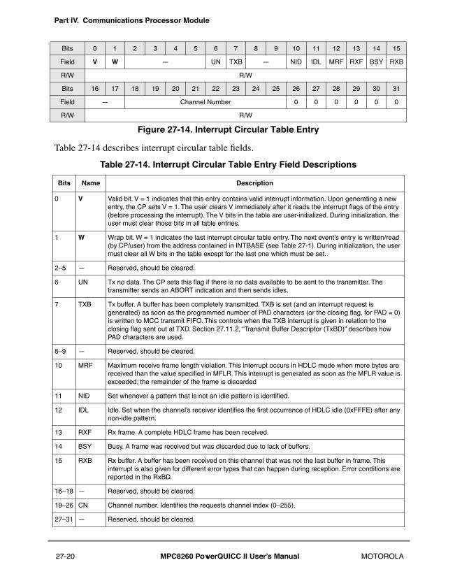
Part IV. Communications Processor Module
Table 27-14 describes interrupt circular table Þelds.
Bits 0 1 2 3 4 5 6 7 8 9 10 11 12 13 14 15
Field V W Ñ UN TXB Ñ NID IDL MRF RXF BSY RXB
R/W R/W
Bits 16 17 18 19 20 21 22 23 24 25 26 27 28 29 30 31
Field Ñ Channel Number 0 0 0 0 0 0
R/W R/W
Figure 27-14. Interrupt Circular Table Entry
Table 27-14. Interrupt Circular Table Entry Field Descriptions
Bits Name Description
0 V Valid bit. V = 1 indicates that this entry contains valid interrupt information. Upon generating a new entry, the CP sets V = 1. The user clears V immediately after it reads the interrupt ßags of the entry (before processing the interrupt). The V bits in the table are user-initialized. During initialization, the user must clear those bits in all table entries.
1 W Wrap bit. W = 1 indicates the last interrupt circular table entry. The next eventÕs entry is written/read (by CP/user) from the address contained in INTBASE (see Table 27-1). During initialization, the user must clear all W bits in the table except for the last one which must be set.
2Ð5 Ñ Reserved, should be cleared.
6 UN Tx no data. The CP sets this ßag if there is no data available to be sent to the transmitter. The transmitter sends an ABORT indication and then sends idles.
7 TXB Tx buffer. A buffer has been completely transmitted. TXB is set (and an interrupt request is generated) as soon as the programmed number of PAD characters (or the closing ßag, for PAD = 0) is written to MCC transmit FIFO. This controls when the TXB interrupt is given in relation to the closing ßag sent out at TXD. Section 27.11.2, ÒTransmit Buffer Descriptor (TxBD)Ó describes how PAD characters are used.
8Ð9 Ñ Reserved, should be cleared.
10 MRF Maximum receive frame length violation. This interrupt occurs in HDLC mode when more bytes are received than the value speciÞed in MFLR. This interrupt is generated as soon as the MFLR value is exceeded; the remainder of the frame is discarded
11 NID Set whenever a pattern that is not an idle pattern is identiÞed.
12 IDL Idle. Set when the channelÕs receiver identiÞes the Þrst occurrence of HDLC idle (0xFFFE) after any non-idle pattern.
13 RXF Rx frame. A complete HDLC frame has been received.
14 BSY Busy. A frame was received but was discarded due to lack of buffers.
15 RXB Rx buffer. A buffer has been received on this channel that was not the last buffer in frame. This interrupt is also given for different error types that can happen during reception. Error conditions are reported in the RxBD.
16Ð18 Ñ Reserved, should be cleared.
19Ð26 CN Channel number. IdentiÞes the requests channel index (0Ð255).
27Ð31 Ñ Reserved, should be cleared.
27-20 MPC8260 PowerQUICC II UserÕs Manual MOTOROLA
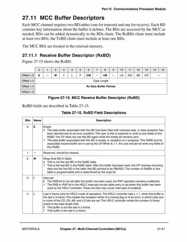
Part IV. Communications Processor Module
27.11 MCC Buffer DescriptorsEach MCC channel requires two BD tables (one for transmit and one for receive). Each BDcontains key information about the buffer it deÞnes. The BDs are accessed by the MCC asneeded; BDs can be added dynamically to the BDs chain. The RxBDs chain must includeat least two BDs; the TxBD chain must include at least one BDs.
The MCC BDs are located in the external memory.
27.11.1 Receive Buffer Descriptor (RxBD)Figure 27-15 shows the RxBD.
RxBD Þelds are described in Table 27-15.
0 1 2 3 4 5 6 7 8 9 10 11 12 13 14 15
Offset + 0 E Ñ W I L F CM Ñ UB Ñ LG NO AB CR Ñ
Offset + 2 Data Length
Offset + 4 Rx Data Buffer Pointer
Offset + 6
Figure 27-15. MCC Receive Buffer Descriptor (RxBD)
Table 27-15. RxBD Field Descriptions
Bits Name Description
0 E Empty0 The data buffer associated with this BD has been Þlled with received data, or data reception has
been aborted due to an error condition. The user is free to examine or write to any Þelds of this RxBD. The CP does not use this BD again while the empty bit remains zero.
1 The data buffer associated with this BD is empty, or reception is in progress. This RxBD and its associated receive buffer are in use by the CP. When E = 1, the user should not write any Þelds of this RxBD.
1 Ñ Reserved, should be cleared.
2 W Wrap (Þnal BD in table)0 This is not the last BD in the RxBD table. 1 This is the last BD in the RxBD table. After this buffer has been used, the CP receives incoming
data into the Þrst BD in the table (the BD pointed to by RBASE). The number of RxBDs in this table is programmable and is determined by the wrap bit.
3 I Interrupt 0 The RXB bit is not set after this buffer has been used, but RXF operation remains unaffected.1 The RXB or RXF bit in the HDLC interrupt circular table entry is set when this buffer has been
used by the HDLC controller. These two bits may cause interrupts (if enabled).
4 L Last in frame (only for HDLC mode of operation). The HDLC controller sets L = 1, when this buffer is the last in a frame. This implies the reception either of a closing ßag or of an error, in which case one or more of the CD, OV, AB, and LG bits are set. The HDLC controller writes the number of frame octets to the data length Þeld.0 This buffer is not the last in a frame. 1 This buffer is the last in a frame.
MOTOROLA Chapter 27. Multi-Channel Controllers (MCCs) 27-21
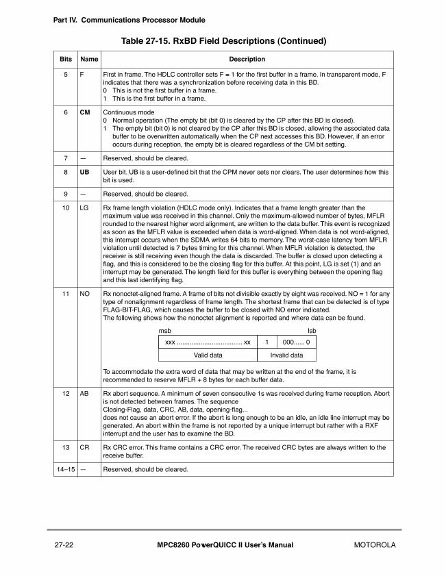
Part IV. Communications Processor Module
5 F First in frame. The HDLC controller sets F = 1 for the Þrst buffer in a frame. In transparent mode, F indicates that there was a synchronization before receiving data in this BD. 0 This is not the Þrst buffer in a frame. 1 This is the Þrst buffer in a frame.
6 CM Continuous mode0 Normal operation (The empty bit (bit 0) is cleared by the CP after this BD is closed).1 The empty bit (bit 0) is not cleared by the CP after this BD is closed, allowing the associated data
buffer to be overwritten automatically when the CP next accesses this BD. However, if an error occurs during reception, the empty bit is cleared regardless of the CM bit setting.
7 Ñ Reserved, should be cleared.
8 UB User bit. UB is a user-deÞned bit that the CPM never sets nor clears. The user determines how this bit is used.
9 Ñ Reserved, should be cleared.
10 LG Rx frame length violation (HDLC mode only). Indicates that a frame length greater than the maximum value was received in this channel. Only the maximum-allowed number of bytes, MFLR rounded to the nearest higher word alignment, are written to the data buffer. This event is recognized as soon as the MFLR value is exceeded when data is word-aligned. When data is not word-aligned, this interrupt occurs when the SDMA writes 64 bits to memory. The worst-case latency from MFLR violation until detected is 7 bytes timing for this channel. When MFLR violation is detected, the receiver is still receiving even though the data is discarded. The buffer is closed upon detecting a ßag, and this is considered to be the closing ßag for this buffer. At this point, LG is set (1) and an interrupt may be generated. The length Þeld for this buffer is everything between the opening ßag and this last identifying ßag.
11 NO Rx nonoctet-aligned frame. A frame of bits not divisible exactly by eight was received. NO = 1 for any type of nonalignment regardless of frame length. The shortest frame that can be detected is of type FLAG-BIT-FLAG, which causes the buffer to be closed with NO error indicated. The following shows how the nonoctet alignment is reported and where data can be found.
To accommodate the extra word of data that may be written at the end of the frame, it is recommended to reserve MFLR + 8 bytes for each buffer data.
12 AB Rx abort sequence. A minimum of seven consecutive 1s was received during frame reception. Abort is not detected between frames. The sequence Closing-Flag, data, CRC, AB, data, opening-ßag... does not cause an abort error. If the abort is long enough to be an idle, an idle line interrupt may be generated. An abort within the frame is not reported by a unique interrupt but rather with a RXF interrupt and the user has to examine the BD.
13 CR Rx CRC error. This frame contains a CRC error. The received CRC bytes are always written to the receive buffer.
14Ð15 Ñ Reserved, should be cleared.
Table 27-15. RxBD Field Descriptions (Continued)
Bits Name Description
msb lsb
1 000...... 0
Valid data Invalid data
xxx .................................... xx
27-22 MPC8260 PowerQUICC II UserÕs Manual MOTOROLA
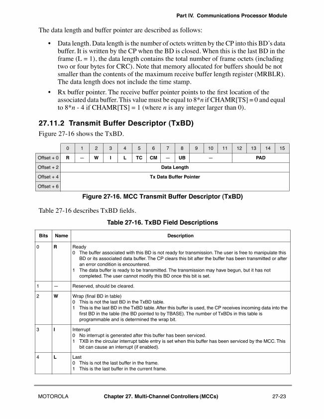
Part IV. Communications Processor Module
The data length and buffer pointer are described as follows:
¥ Data length. Data length is the number of octets written by the CP into this BDÕs data buffer. It is written by the CP when the BD is closed. When this is the last BD in the frame (L = 1), the data length contains the total number of frame octets (including two or four bytes for CRC). Note that memory allocated for buffers should be not smaller than the contents of the maximum receive buffer length register (MRBLR). The data length does not include the time stamp.
¥ Rx buffer pointer. The receive buffer pointer points to the Þrst location of the associated data buffer. This value must be equal to 8*n if CHAMR[TS] = 0 and equal to 8*n - 4 if CHAMR[TS] = 1 (where n is any integer larger than 0).
27.11.2 Transmit Buffer Descriptor (TxBD)Figure 27-16 shows the TxBD.
Table 27-16 describes TxBD Þelds.
0 1 2 3 4 5 6 7 8 9 10 11 12 13 14 15
Offset + 0 R Ñ W I L TC CM Ñ UB Ñ PAD
Offset + 2 Data Length
Offset + 4 Tx Data Buffer Pointer
Offset + 6
Figure 27-16. MCC Transmit Buffer Descriptor (TxBD)
Table 27-16. TxBD Field Descriptions
Bits Name Description
0 R Ready0 The buffer associated with this BD is not ready for transmission. The user is free to manipulate this
BD or its associated data buffer. The CP clears this bit after the buffer has been transmitted or after an error condition is encountered.
1 The data buffer is ready to be transmitted. The transmission may have begun, but it has not completed. The user cannot modify this BD once this bit is set.
1 Ñ Reserved, should be cleared.
2 W Wrap (Þnal BD in table)0 This is not the last BD in the TxBD table. 1 This is the last BD in the TxBD table. After this buffer is used, the CP receives incoming data into the
Þrst BD in the table (the BD pointed to by TBASE). The number of TxBDs in this table is programmable and is determined the wrap bit.
3 I Interrupt 0 No interrupt is generated after this buffer has been serviced. 1 TXB in the circular interrupt table entry is set when this buffer has been serviced by the MCC. This
bit can cause an interrupt (if enabled).
4 L Last 0 This is not the last buffer in the frame. 1 This is the last buffer in the current frame.
MOTOROLA Chapter 27. Multi-Channel Controllers (MCCs) 27-23
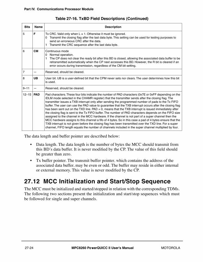
Part IV. Communications Processor Module
The data length and buffer pointer are described below:
¥ Data length. The data length is the number of bytes the MCC should transmit from this BDÕs data buffer. It is never modiÞed by the CP. The value of this Þeld should be greater than zero.
¥ Tx buffer pointer. The transmit buffer pointer, which contains the address of the associated data buffer, may be even or odd. The buffer may reside in either internal or external memory. This value is never modiÞed by the CP.
27.12 MCC Initialization and Start/Stop SequenceThe MCC must be initialized and started/stopped in relation with the corresponding TDMs.The following two sections present the initialization and start/stop sequences which mustbe followed for single and super channels.
5 F Tx CRC. Valid only when L = 1. Otherwise it must be ignored.0 Transmit the closing ßag after the last data byte. This setting can be used for testing purposes to
send an erroneous CRC after the data. 1 Transmit the CRC sequence after the last data byte.
6 CM Continuous mode0 Normal operation.1 The CP does not clear the ready bit after this BD is closed, allowing the associated data buffer to be
retransmitted automatically when the CP next accesses this BD. However, the R bit is cleared if an error occurs during transmission, regardless of the CM bit setting.
7 Ñ Reserved, should be cleared.
8 UB User bit. UB is a user-deÞned bit that the CPM never sets nor clears. The user determines how this bit is used.
9Ð11 Ñ Reserved, should be cleared.
12Ð15 PAD Pad characters. These four bits indicate the number of PAD characters (0x7E or 0xFF depending on the IDLM mode selected in the CHAMR register) that the transmitter sends after the closing ßag. The transmitter issues a TXB interrupt only after sending the programmed number of pads to the Tx FIFO buffer. The user can use the PAD value to guarantee that the TXB interrupt occurs after the closing ßag has been sent out on the TXD line. PAD = 0, means that the TXB interrupt is issued immediately after the closing ßag is sent to the Tx FIFO buffer. The number of PAD characters depends on the FIFO size assigned to the channel in the MCC hardware. If the channel is not part of a super channel then the MCC hardware assigns to this channel a Þfo of 4 bytes. So in this case a pad of 4 bytes ensure that the TXB interrupt is not given before the closing ßag has been transmitted over the TXD line. For a super channel, FIFO length equals the number of channels included in the super channel multiplied by four.
Table 27-16. TxBD Field Descriptions (Continued)
Bits Name Description
27-24 MPC8260 PowerQUICC II UserÕs Manual MOTOROLA
Part IV. Communications Processor Module
27.12.1 Single-Channel InitializationThe following sequence must be followed to initialize and start a single channel (after resetor after a fatal error):
1. Program the SI. The entries the MCC channels uses must point to the null channel (set in the SI RAM entry MCC = 0, CSEL = 0 and the correct size - 1 byte); entries used by other controllers (not MCC) can be activated at this time.
2. Initialize the MCC parameters (in DPR and external memory).
3. Enable the MCC channel as described in Section 27.6.1, ÒInternal Transmitter State (TSTATE),Ó and Section 27.6.4, ÒInternal Receiver State (RSTATE).Ó
4. Reprogram the SI RAM to point to the enabled channel(s).
The following sequence must be followed to stop a single channel in order to change the SIwithout using the shadow SI:
1. Issue a STOP command for the respective channel as described in Section 27.9, ÒMCC Commands.Ó
2. Change the SI.
3. Enable the MCC channel(s) as described in Section 27.6.1, ÒInternal Transmitter State (TSTATE),Ó and Section 27.6.4, ÒInternal Receiver State (RSTATE).Ó
It is possible to change the SI using the SI shadow while the channel is active. Both theprimary and the shadow conÞguration of the SI RAM must observe the conÞgurationdeÞned in MCCF (see Section 27.8, ÒMCC ConÞguration Registers (MCCFx)Ó). TheMCCF cannot be changed while there are active channels.
The following sequence must be followed to stop a single channel in order to change theMCC parameters of the respective channel:
1. Issue a STOP command for the respective channel as described in Section 27.9, ÒMCC Commands,Ó or change the associated SI RAM entry to point to a channel which is not active and wait for two frame periods in order to clear the internal FIFOs.
2. Change the channel parameters.
3. Enable the MCC channel(s) as described in Section 27.6.1, ÒInternal Transmitter State (TSTATE),Ó and Section 27.6.4, ÒInternal Receiver State (RSTATE),Ó or change the associated SI RAM entry to point to the respective channel.
MOTOROLA Chapter 27. Multi-Channel Controllers (MCCs) 27-25
Part IV. Communications Processor Module
27.12.2 Super Channel InitializationThe following steps initialize and start a super channel (after reset of after a fatal error):
1. Program the SI as required for a super channel but do not enable the TDM.
2. Issue a STOP command as described in Section 27.9, ÒMCC Commands.Ó
3. Enable the TDM.
4. Initialize the MCC parameters (in DPR and external memory).
5. Enable the MCC channel(s) as described in Section 27.6.1, ÒInternal Transmitter State (TSTATE),Ó and Section 27.6.4, ÒInternal Receiver State (RSTATE).Ó
The following sequence must be followed to stop a super channel in order to change the SI:
1. Issue a STOP command for the respective channel as described in Section 27.9, ÒMCC Commands.Ó
2. Disable the TDM.
3. Change the SI.
4. Enable the TDM.
5. If necessary, change the MCC parameters (in DPR and external memory).
6. Enable the MCC channel(s) as described in Section 27.6.1, ÒInternal Transmitter State (TSTATE),Ó and Section 27.6.4, ÒInternal Receiver State (RSTATE).Ó
Under the following restrictions, the SI can be changed using the SI shadow while thechannel is active:
¥ Both the primary and the shadow conÞguration of the SI RAM must observe the conÞguration of the super channel. Note that the super-channel table and MCCF register cannot be changed dynamically.
¥ It is not possible to add dynamically to a super channel a time slot previously used by a single-channel and had a width different from 8 bits.
¥ A time slot that was previously used by a single channel and had a width different from 8 bits cannot be added dynamically to a super channel.
27.13 MCC Latency and PerformanceThe MCC transfers data to/from the memory 8 bytes at a time. Considering this and theinternal receiver FIFO (of 2 bytes/channel), the receiver latency (time since data on achannel is serialized until the respective data is written to memory) can be from 8Ð10 frameperiods.
If no super channels are active, the MCC can handle aggregate data rates of up to 16 Mbpson each of the four channel subgroups. If super channels are used this performance islimited to 8 Mbps.
27-26 MPC8260 PowerQUICC II UserÕs Manual MOTOROLA
Part IV. Communications Processor Module
If multiple synchronized channels are used (as an example 8 T1 with common clock/sync)it is recommended to start the channels out of phase in order to load uniformly the bus. Thisavoids bus activity peaks when all the channels have to transfer data to/from the memorysimultaneously.
MOTOROLA Chapter 27. Multi-Channel Controllers (MCCs) 27-27

Part IV. Communications Processor Module
27-28 MPC8260 PowerQUICC II UserÕs Manual MOTOROLA
Chapter 28 Fast Communications Controllers (FCCs)280280
The MPC8260Õs fast communications controllers (FCCs) are serial communicationscontrollers (SCCs) optimized for synchronous high-rate protocols. FCC key featuresinclude the following:
¥ Supports HDLC/SDLC and totally transparent protocols
¥ FCC clocks can be derived from a baud-rate generator or an external signal.
¥ Supports RTS, CTS, and CD modem control signals
¥ Use of bursts to improve bus usage
¥ Multibuffer data structure for receive and transmit, external buffer descriptors (BDs) anywhere in system memory
¥ 192-byte FIFO buffers
¥ Full-duplex operation
¥ Fully transparent option for one half of an FCC (receiver/transmitter) while HDLC/SDLC protocol executes on the other half (transmitter/receiver)
¥ Echo and local loopback modes for testing
¥ Assuming a 100-MHz CPM clock, the FCCs support the following:
Ñ Full 10/100-Mbps Ethernet/IEEE 802.3x through an MII
Ñ Full 155-Mbps ATM segmentation and reassembly (SAR) through UTOPIA (on FCC1 and FCC2 only)
Ñ 45-Mbps (DS-3/E3 rates) HDLC and/or transparent data rates supported on each FCC
FCCs differ from SCCs as follows:
¥ No DPLL support.
¥ No BISYNC, UART, or AppleTalk/LocalTalk support.
¥ No HDLC bus.
¥ Ethernet support only through an MII.
MOTOROLA Chapter 28. Fast Communications Controllers (FCCs) 28-1
Part IV. Communications Processor Module
28.1 OverviewMPC8260 FCCs can be conÞgured independently to implement different protocols.Together, they can be used to implement bridging functions, routers, and gateways, and tointerface with a wide variety of standard WANs, LANs, and proprietary networks. FCCshave many physical interface options such as interfacing to TDM buses, ISDN buses,standard modem interfaces, fast Ethernet interface (MII), and ATM interfaces (UTOPIA);see Chapter 14, ÒSerial Interface with Time-Slot Assigner,Ó Chapter 30, ÒFast EthernetController,Ó and Chapter 29, ÒATM Controller.Ó The FCCs are independent from thephysical interface, but FCC logic formats and manipulates data from the physical interface.That is why the interfaces are described separately.
The FCC is described in terms of the protocol that it is chosen to run. When an FCC isprogrammed to a certain protocol, it implements a certain level of functionality associatedwith that protocol. For most protocols, this corresponds to portions of the link layer (layer2 of the seven-layer OSI model). Many functions of the FCC are common to all of theprotocols. These functions are described in the FCC description. Following that, theimplementation details that differentiate protocols from one another are discussed,beginning with the transparent protocol. Thus, the reader should read from this point to thetransparent protocol and then skip to the appropriate protocol. Since the FCCs use similardata structures across all protocols, the reader's learning time decreases dramatically afterunderstanding the Þrst protocol.
Each FCC supports a number of protocolsÑEthernet, HDLC/SDLC, ATM, and totallytransparent operation. Although the selected protocol usually applies to both the FCCtransmitter and receiver, half of one FCC can run transparent operation while the other runsHDLC/SDLC protocol. The internal clocks (RCLK, TCLK) for each FCC can beprogrammed with either an external or internal source. The internal clocks originate fromone of the baud-rate generators or one of the external clock signals. These clocks can be asfast as one-third the CPM clock frequency. See Chapter 14, ÒSerial Interface with Time-Slot Assigner.Ó However, the FCCÕs ability to support a sustained bit stream depends on theprotocol as well as on other factors.Each FCC can be connected to its own set of pins onthe MPC8260. This conÞguration, the nonmultiplexed serial interface, or NMSI, isdescribed in Chapter 14, ÒSerial Interface with Time-Slot Assigner.Ó In this conÞguration,each FCC can support the standard modem interface signals (RTS, CTS, and CD) throughthe appropriate port pins and the interrupt controller. Additional handshake signals can besupported with additional parallel I/O lines. The FCC block diagram is shown inFigure 28-1.
28-2 MPC8260 PowerQUICC II UserÕs Manual MOTOROLA
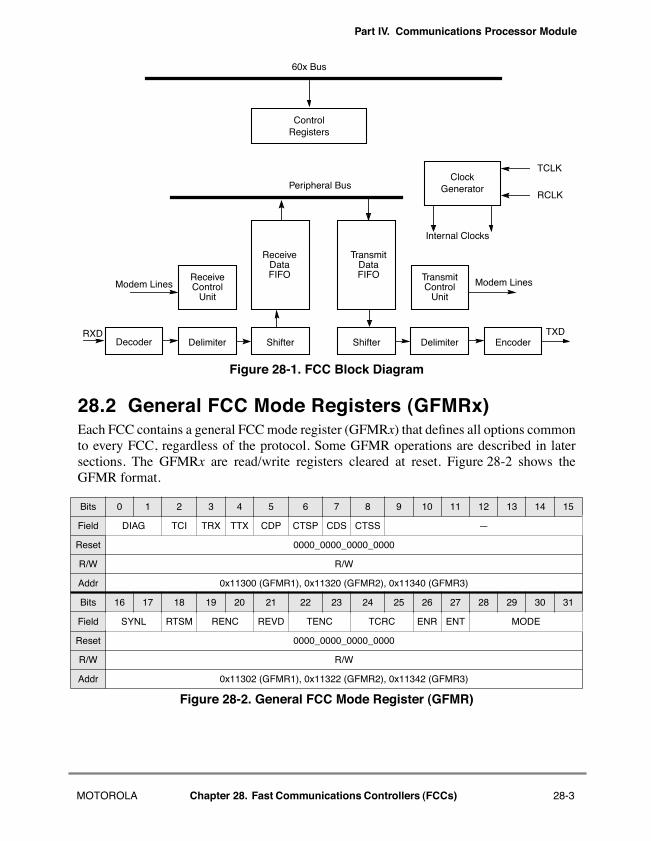
Part IV. Communications Processor Module
Figure 28-1. FCC Block Diagram
28.2 General FCC Mode Registers (GFMRx)Each FCC contains a general FCC mode register (GFMRx) that deÞnes all options commonto every FCC, regardless of the protocol. Some GFMR operations are described in latersections. The GFMRx are read/write registers cleared at reset. Figure 28-2 shows theGFMR format.
Bits 0 1 2 3 4 5 6 7 8 9 10 11 12 13 14 15
Field DIAG TCI TRX TTX CDP CTSP CDS CTSS Ñ
Reset 0000_0000_0000_0000
R/W R/W
Addr 0x11300 (GFMR1), 0x11320 (GFMR2), 0x11340 (GFMR3)
Bits 16 17 18 19 20 21 22 23 24 25 26 27 28 29 30 31
Field SYNL RTSM RENC REVD TENC TCRC ENR ENT MODE
Reset 0000_0000_0000_0000
R/W R/W
Addr 0x11302 (GFMR1), 0x11322 (GFMR2), 0x11342 (GFMR3)
Figure 28-2. General FCC Mode Register (GFMR)
ControlRegisters
ShifterShifter Delimiter
ClockGenerator
DelimiterDecoder Encoder
ReceiveControl
Unit
TransmitControl
Unit
ReceiveDataFIFO
TransmitDataFIFO
Modem LinesModem Lines
60x Bus
Peripheral Bus
TCLK
RCLK
Internal Clocks
RXD TXD
MOTOROLA Chapter 28. Fast Communications Controllers (FCCs) 28-3
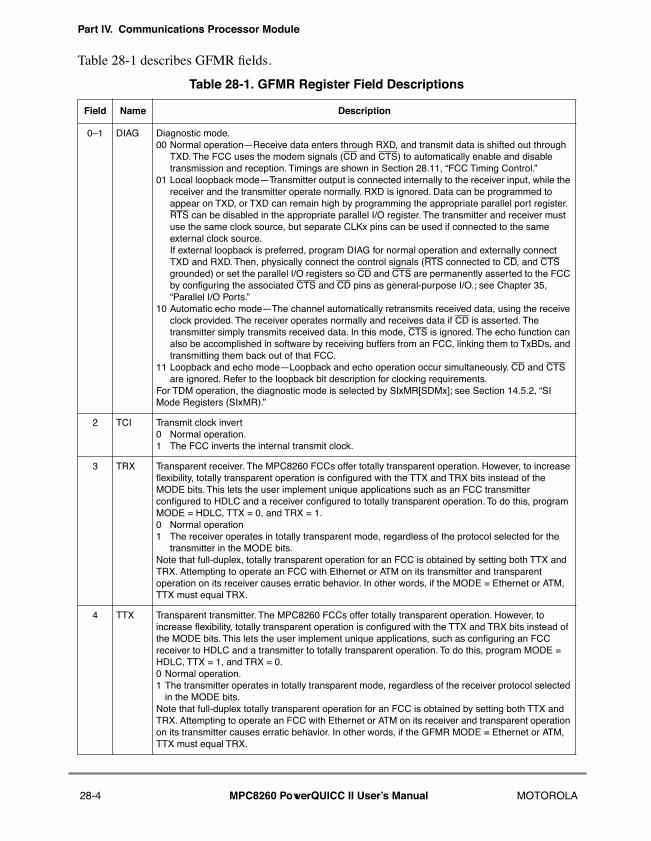
Part IV. Communications Processor Module
Table 28-1 describes GFMR Þelds.
Table 28-1. GFMR Register Field Descriptions
Field Name Description
0Ð1 DIAG Diagnostic mode. 00 Normal operationÑReceive data enters through RXD, and transmit data is shifted out through
TXD. The FCC uses the modem signals (CD and CTS) to automatically enable and disable transmission and reception. Timings are shown in Section 28.11, ÒFCC Timing Control.Ó
01 Local loopback modeÑTransmitter output is connected internally to the receiver input, while the receiver and the transmitter operate normally. RXD is ignored. Data can be programmed to appear on TXD, or TXD can remain high by programming the appropriate parallel port register. RTS can be disabled in the appropriate parallel I/O register. The transmitter and receiver must use the same clock source, but separate CLKx pins can be used if connected to the same external clock source.If external loopback is preferred, program DIAG for normal operation and externally connect TXD and RXD. Then, physically connect the control signals (RTS connected to CD, and CTS grounded) or set the parallel I/O registers so CD and CTS are permanently asserted to the FCC by conÞguring the associated CTS and CD pins as general-purpose I/O.; see Chapter 35, ÒParallel I/O Ports.Ó
10 Automatic echo modeÑThe channel automatically retransmits received data, using the receive clock provided. The receiver operates normally and receives data if CD is asserted. The transmitter simply transmits received data. In this mode, CTS is ignored. The echo function can also be accomplished in software by receiving buffers from an FCC, linking them to TxBDs, and transmitting them back out of that FCC.
11 Loopback and echo modeÑLoopback and echo operation occur simultaneously. CD and CTS are ignored. Refer to the loopback bit description for clocking requirements.
For TDM operation, the diagnostic mode is selected by SIxMR[SDMx]; see Section 14.5.2, ÒSI Mode Registers (SIxMR).Ó
2 TCI Transmit clock invert0 Normal operation.1 The FCC inverts the internal transmit clock.
3 TRX Transparent receiver. The MPC8260 FCCs offer totally transparent operation. However, to increase ßexibility, totally transparent operation is conÞgured with the TTX and TRX bits instead of the MODE bits. This lets the user implement unique applications such as an FCC transmitter conÞgured to HDLC and a receiver conÞgured to totally transparent operation. To do this, program MODE = HDLC, TTX = 0, and TRX = 1.0 Normal operation1 The receiver operates in totally transparent mode, regardless of the protocol selected for the
transmitter in the MODE bits.Note that full-duplex, totally transparent operation for an FCC is obtained by setting both TTX and TRX. Attempting to operate an FCC with Ethernet or ATM on its transmitter and transparent operation on its receiver causes erratic behavior. In other words, if the MODE = Ethernet or ATM, TTX must equal TRX.
4 TTX Transparent transmitter. The MPC8260 FCCs offer totally transparent operation. However, to increase ßexibility, totally transparent operation is conÞgured with the TTX and TRX bits instead of the MODE bits. This lets the user implement unique applications, such as conÞguring an FCC receiver to HDLC and a transmitter to totally transparent operation. To do this, program MODE = HDLC, TTX = 1, and TRX = 0.0 Normal operation.1 The transmitter operates in totally transparent mode, regardless of the receiver protocol selected
in the MODE bits.Note that full-duplex totally transparent operation for an FCC is obtained by setting both TTX and TRX. Attempting to operate an FCC with Ethernet or ATM on its receiver and transparent operation on its transmitter causes erratic behavior. In other words, if the GFMR MODE = Ethernet or ATM, TTX must equal TRX.
28-4 MPC8260 PowerQUICC II UserÕs Manual MOTOROLA
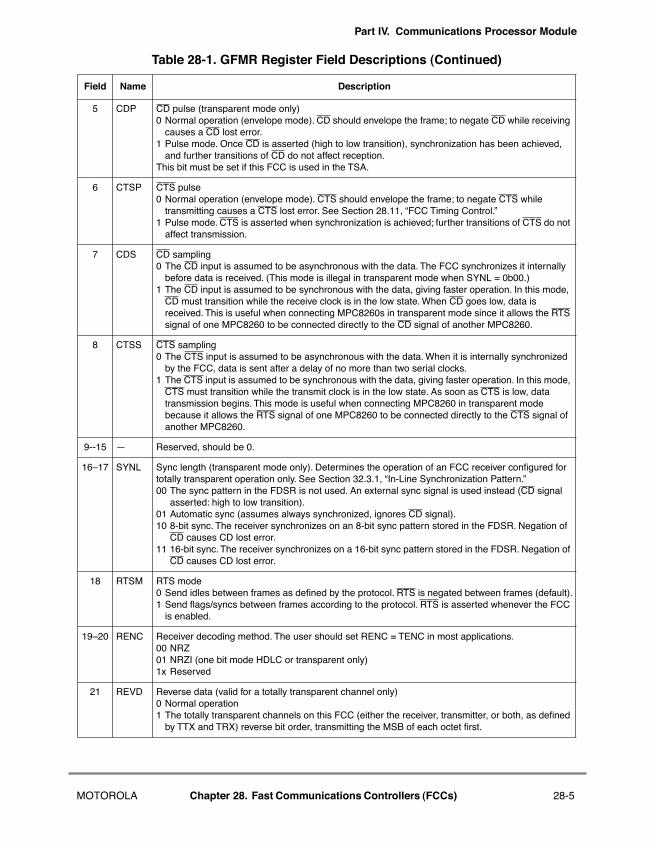
Part IV. Communications Processor Module
5 CDP CD pulse (transparent mode only)0 Normal operation (envelope mode). CD should envelope the frame; to negate CD while receiving
causes a CD lost error. 1 Pulse mode. Once CD is asserted (high to low transition), synchronization has been achieved,
and further transitions of CD do not affect reception. This bit must be set if this FCC is used in the TSA.
6 CTSP CTS pulse0 Normal operation (envelope mode). CTS should envelope the frame; to negate CTS while
transmitting causes a CTS lost error. See Section 28.11, ÒFCC Timing Control.Ó1 Pulse mode. CTS is asserted when synchronization is achieved; further transitions of CTS do not
affect transmission.
7 CDS CD sampling0 The CD input is assumed to be asynchronous with the data. The FCC synchronizes it internally
before data is received. (This mode is illegal in transparent mode when SYNL = 0b00.)1 The CD input is assumed to be synchronous with the data, giving faster operation. In this mode,
CD must transition while the receive clock is in the low state. When CD goes low, data is received. This is useful when connecting MPC8260s in transparent mode since it allows the RTS signal of one MPC8260 to be connected directly to the CD signal of another MPC8260.
8 CTSS CTS sampling0 The CTS input is assumed to be asynchronous with the data. When it is internally synchronized
by the FCC, data is sent after a delay of no more than two serial clocks.1 The CTS input is assumed to be synchronous with the data, giving faster operation. In this mode,
CTS must transition while the transmit clock is in the low state. As soon as CTS is low, data transmission begins. This mode is useful when connecting MPC8260 in transparent mode because it allows the RTS signal of one MPC8260 to be connected directly to the CTS signal of another MPC8260.
9--15 Ñ Reserved, should be 0.
16Ð17 SYNL Sync length (transparent mode only). Determines the operation of an FCC receiver conÞgured for totally transparent operation only. See Section 32.3.1, ÒIn-Line Synchronization Pattern.Ó00 The sync pattern in the FDSR is not used. An external sync signal is used instead (CD signal
asserted: high to low transition).01 Automatic sync (assumes always synchronized, ignores CD signal).10 8-bit sync. The receiver synchronizes on an 8-bit sync pattern stored in the FDSR. Negation of
CD causes CD lost error.11 16-bit sync. The receiver synchronizes on a 16-bit sync pattern stored in the FDSR. Negation of
CD causes CD lost error.
18 RTSM RTS mode0 Send idles between frames as deÞned by the protocol. RTS is negated between frames (default).1 Send ßags/syncs between frames according to the protocol. RTS is asserted whenever the FCC
is enabled.
19Ð20 RENC Receiver decoding method. The user should set RENC = TENC in most applications.00 NRZ01 NRZI (one bit mode HDLC or transparent only)1x Reserved
21 REVD Reverse data (valid for a totally transparent channel only)0 Normal operation1 The totally transparent channels on this FCC (either the receiver, transmitter, or both, as deÞned
by TTX and TRX) reverse bit order, transmitting the MSB of each octet Þrst.
Table 28-1. GFMR Register Field Descriptions (Continued)
Field Name Description
MOTOROLA Chapter 28. Fast Communications Controllers (FCCs) 28-5
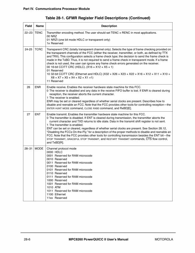
Part IV. Communications Processor Module
22Ð23 TENC Transmitter encoding method. The user should set TENC = RENC in most applications.00 NRZ01 NRZI (one bit mode HDLC or transparent only)1x Reserved
24-25 TCRC Transparent CRC (totally transparent channel only). Selects the type of frame checking provided on the transparent channels of the FCC (either the receiver, transmitter, or both, as deÞned by TTX and TRX). This conÞguration selects a frame check type; the decision to send the frame check is made in the TxBD. Thus, it is not required to send a frame check in transparent mode. If a frame check is not used, the user can ignore any frame check errors generated on the receiver.00 16-bit CCITT CRC (HDLC). (X16 + X12 + X5 + 1)01 Reserved10 32-bit CCITT CRC (Ethernet and HDLC) (X32 + X26 + X23 + X22 + X16 + X12 + X11 + X10 +
X8 + X7 + X5 + X4 + X2 + X1 +1)11 Reserved
26 ENR Enable receive. Enables the receiver hardware state machine for this FCC. 0 The receiver is disabled and any data in the receive FIFO buffer is lost. If ENR is cleared during
reception, the receiver aborts the current character. 1 The receiver is enabled.ENR may be set or cleared regardless of whether serial clocks are present. Describes how to disable and reenable an FCC. Note that the FCC provides other tools for controlling receptionÑthe ENTER HUNT MODE command, CLOSE RXBD command, and RxBD[E].
27 ENT Enable transmit. Enables the transmitter hardware state machine for this FCC. 0 The transmitter is disabled. If ENT is cleared during transmission, the transmitter aborts the
current character and TXD returns to idle state. Data in the transmit shift register is not sent. 1 The transmitter is enabled.ENT can be set or cleared, regardless of whether serial clocks are present. See Section 28.12, ÒDisabling the FCCs On-the-Fly,Ó for a description of the proper methods to disable and reenable an FCC. Note that the FCC provides other tools for controlling transmission besides the ENT bitÑthe STOP TRANSMIT, GRACEFUL STOP TRANSMIT, and RESTART TRANSMIT commands, CTS ßow control, and TxBD[R].
28Ð31 MODE Channel protocol mode0000 HDLC0001 Reserved for RAM microcode0010 Reserved0011 Reserved for RAM microcode0100 Reserved0101 Reserved for RAM microcode0110 Reserved0111 Reserved for RAM microcode1000 Reserved1001 Reserved for RAM microcode1010 ATM1011 Reserved for RAM microcode1100 Ethernet11xx Reserved
Table 28-1. GFMR Register Field Descriptions (Continued)
Field Name Description
28-6 MPC8260 PowerQUICC II UserÕs Manual MOTOROLA
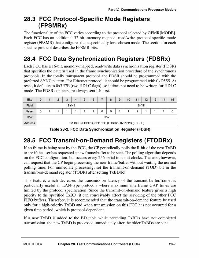
Part IV. Communications Processor Module
28.3 FCC Protocol-SpeciÞc Mode Registers (FPSMRx)
The functionality of the FCC varies according to the protocol selected by GFMR[MODE].Each FCC has an additional 32-bit, memory-mapped, read/write protocol-speciÞc moderegister (FPSMR) that conÞgures them speciÞcally for a chosen mode. The section for eachspeciÞc protocol describes the FPSMR bits.
28.4 FCC Data Synchronization Registers (FDSRx)Each FCC has a 16-bit, memory-mapped, read/write data synchronization register (FDSR)that speciÞes the pattern used in the frame synchronization procedure of the synchronousprotocols. In the totally transparent protocol, the FDSR should be programmed with thepreferred SYNC pattern. For Ethernet protocol, it should be programmed with 0xD555. Atreset, it defaults to 0x7E7E (two HDLC ßags), so it does not need to be written for HDLCmode. The FDSR contents are always sent lsb Þrst.
28.5 FCC Transmit-on-Demand Registers (FTODRx)If no frame is being sent by the FCC, the CP periodically polls the R bit of the next TxBDto see if the user has requested a new frame/buffer to be sent. The polling algorithm dependson the FCC conÞguration, but occurs every 256 serial transmit clocks. The user, however,can request that the CP begin processing the new frame/buffer without waiting the normalpolling time. For immediate processing, set the transmit-on-demand (TOD) bit in thetransmit-on-demand register (TODR) after setting TxBD[R].
This feature, which decreases the transmission latency of the transmit buffer/frame, isparticularly useful in LAN-type protocols where maximum interframe GAP times arelimited by the protocol speciÞcation. Since the transmit-on-demand feature gives a highpriority to the speciÞed TxBD, it can conceivably affect the servicing of the other FCCFIFO buffers. Therefore, it is recommended that the transmit-on-demand feature be usedonly for a high-priority TxBD and when transmission on this FCC has not occurred for agiven time period, which is protocol-dependent.
If a new TxBD is added to the BD table while preceding TxBDs have not completedtransmission, the new TxBD is processed immediately after the older TxBDs are sent.
Bits 0 1 2 3 4 5 6 7 8 9 10 11 12 13 14 15
Field SYN2 SYN1
Reset 0 1 1 1 1 1 1 0 0 1 1 1 1 1 1 0
R/W R/W
Address 0x1130C (FDSR1), 0x1132C (FDSR2), 0x1132C (FDSR3)
Table 28-2. FCC Data Synchronization Register (FDSR)
MOTOROLA Chapter 28. Fast Communications Controllers (FCCs) 28-7
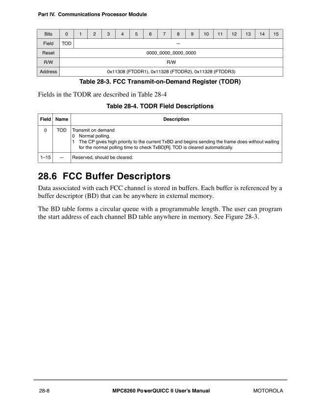
Part IV. Communications Processor Module
Fields in the TODR are described in Table 28-4
28.6 FCC Buffer DescriptorsData associated with each FCC channel is stored in buffers. Each buffer is referenced by abuffer descriptor (BD) that can be anywhere in external memory.
The BD table forms a circular queue with a programmable length. The user can programthe start address of each channel BD table anywhere in memory. See Figure 28-3.
Bits 0 1 2 3 4 5 6 7 8 9 10 11 12 13 14 15
Field TOD Ñ
Reset 0000_0000_0000_0000
R/W R/W
Address 0x11308 (FTODR1), 0x11328 (FTODR2), 0x11328 (FTODR3)
Table 28-3. FCC Transmit-on-Demand Register (TODR)
Table 28-4. TODR Field Descriptions
Field Name Description
0 TOD Transmit on demand0 Normal polling.1 The CP gives high priority to the current TxBD and begins sending the frame does without waiting
for the normal polling time to check TxBD[R]. TOD is cleared automatically.
1Ð15 Ñ Reserved, should be cleared.
28-8 MPC8260 PowerQUICC II UserÕs Manual MOTOROLA
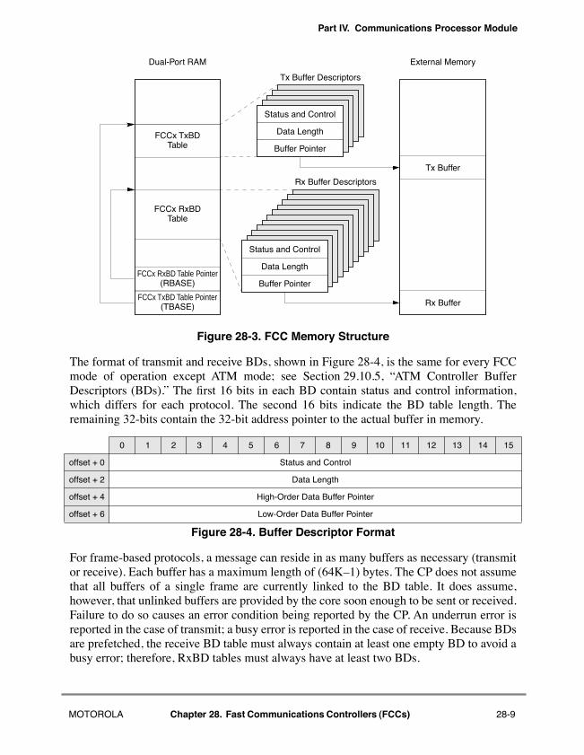
Part IV. Communications Processor Module
Figure 28-3. FCC Memory Structure
The format of transmit and receive BDs, shown in Figure 28-4, is the same for every FCCmode of operation except ATM mode; see Section 29.10.5, ÒATM Controller BufferDescriptors (BDs).Ó The Þrst 16 bits in each BD contain status and control information,which differs for each protocol. The second 16 bits indicate the BD table length. Theremaining 32-bits contain the 32-bit address pointer to the actual buffer in memory.
For frame-based protocols, a message can reside in as many buffers as necessary (transmitor receive). Each buffer has a maximum length of (64KÐ1) bytes. The CP does not assumethat all buffers of a single frame are currently linked to the BD table. It does assume,however, that unlinked buffers are provided by the core soon enough to be sent or received.Failure to do so causes an error condition being reported by the CP. An underrun error isreported in the case of transmit; a busy error is reported in the case of receive. Because BDsare prefetched, the receive BD table must always contain at least one empty BD to avoid abusy error; therefore, RxBD tables must always have at least two BDs.
0 1 2 3 4 5 6 7 8 9 10 11 12 13 14 15
offset + 0 Status and Control
offset + 2 Data Length
offset + 4 High-Order Data Buffer Pointer
offset + 6 Low-Order Data Buffer Pointer
Figure 28-4. Buffer Descriptor Format
Status and Control
Data Length
Buffer Pointer
FCCx TxBD Table Pointer(TBASE)
FCCx RxBD Table Pointer(RBASE)
FCCx RxBDTable
FCCx TxBDTable
Dual-Port RAM
Status and Control
Data Length
Buffer Pointer
Tx Buffer
External Memory
Rx Buffer Descriptors
Tx Buffer Descriptors
Rx Buffer
MOTOROLA Chapter 28. Fast Communications Controllers (FCCs) 28-9
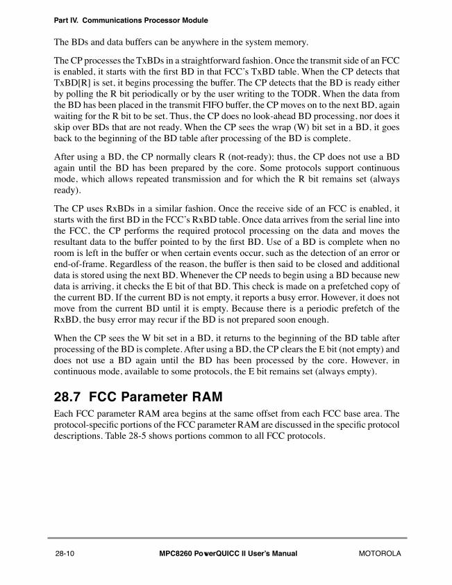
Part IV. Communications Processor Module
The BDs and data buffers can be anywhere in the system memory.
The CP processes the TxBDs in a straightforward fashion. Once the transmit side of an FCCis enabled, it starts with the Þrst BD in that FCCÕs TxBD table. When the CP detects thatTxBD[R] is set, it begins processing the buffer. The CP detects that the BD is ready eitherby polling the R bit periodically or by the user writing to the TODR. When the data fromthe BD has been placed in the transmit FIFO buffer, the CP moves on to the next BD, againwaiting for the R bit to be set. Thus, the CP does no look-ahead BD processing, nor does itskip over BDs that are not ready. When the CP sees the wrap (W) bit set in a BD, it goesback to the beginning of the BD table after processing of the BD is complete.
After using a BD, the CP normally clears R (not-ready); thus, the CP does not use a BDagain until the BD has been prepared by the core. Some protocols support continuousmode, which allows repeated transmission and for which the R bit remains set (alwaysready).
The CP uses RxBDs in a similar fashion. Once the receive side of an FCC is enabled, itstarts with the Þrst BD in the FCCÕs RxBD table. Once data arrives from the serial line intothe FCC, the CP performs the required protocol processing on the data and moves theresultant data to the buffer pointed to by the Þrst BD. Use of a BD is complete when noroom is left in the buffer or when certain events occur, such as the detection of an error orend-of-frame. Regardless of the reason, the buffer is then said to be closed and additionaldata is stored using the next BD. Whenever the CP needs to begin using a BD because newdata is arriving, it checks the E bit of that BD. This check is made on a prefetched copy ofthe current BD. If the current BD is not empty, it reports a busy error. However, it does notmove from the current BD until it is empty. Because there is a periodic prefetch of theRxBD, the busy error may recur if the BD is not prepared soon enough.
When the CP sees the W bit set in a BD, it returns to the beginning of the BD table afterprocessing of the BD is complete. After using a BD, the CP clears the E bit (not empty) anddoes not use a BD again until the BD has been processed by the core. However, incontinuous mode, available to some protocols, the E bit remains set (always empty).
28.7 FCC Parameter RAMEach FCC parameter RAM area begins at the same offset from each FCC base area. Theprotocol-speciÞc portions of the FCC parameter RAM are discussed in the speciÞc protocoldescriptions. Table 28-5 shows portions common to all FCC protocols.
28-10 MPC8260 PowerQUICC II UserÕs Manual MOTOROLA
Part IV. Communications Processor Module
Some parameter RAM values must be initialized before the FCC is enabled; other valuesare initialized/written by the CP. Once initialized, most parameter RAM values do not needto be accessed by user software because most activity centers around the TxBDs andRxBDs rather than the parameter RAM. However, if the parameter RAM is accessed, notethe following:
¥ Parameter RAM can be read at any time.
¥ Tx parameter RAM can be written only when the transmitter is disabledÑafter a STOP TRANSMIT command and before a RESTART TRANSMIT command or after the buffer/frame Þnishes transmitting after a GRACEFUL STOP TRANSMIT command and before a RESTART TRANSMIT command.
¥ Rx parameter RAM can be written only when the receiver is disabled. Note the CLOSE RXBD command does not stop reception, but it does allow the user to extract data from a partially full Rx buffer.
¥ See Section 28.12, ÒDisabling the FCCs On-the-Fly.Ó
Some parameters in Table 28-5 are not described and are listed only to provide informationfor experienced users and for debugging. The user need not access these parameters innormal operation.
Table 28-5. FCC Parameter RAM Common to All Protocols
Offset1 Name Width Description
0x00 RIPTR Hword Receive internal temporary data pointer. Used by microcode as a temporary buffer for data. Must be 32-byte aligned and the size of the internal buffer must be 32 bytes unless it is stated otherwise in the protocol speciÞcation. For best performance, it should be located in the following address ranges: 0x3000Ð0x4000 or 0xB000Ð0xC000.
0x02 TIPTR Hword Transmit internal temporary data pointer. Used by microcode as a temporary buffer for data. Must be 32-byte aligned and the size of the internal buffer must be 32 bytes unless it is stated otherwise in the protocol speciÞcation. For best performance it should be located in the following address ranges: 0x3000Ð0x4000 or 0xB000Ð0xC000.
0x04 Ñ Hword Reserved, should be cleared.
0x06 MRBLR Hword Maximum receive buffer length (a multiple of 32 for all modes). The number of bytes that the FCC receiver writes to a receive buffer before moving to the next buffer. The receiver can write fewer bytes to the buffer than MRBLR if a condition such as an error or end-of-frame occurs, but it never exceeds the MRBLR value. Therefore, user-supplied buffers should be at least as large as the MRBLR. Note that FCC transmit buffers can have varying lengths by programming TxBD[Data Length], as needed, and are not affected by the value in MRBLR. MRBLR is not intended to be changed dynamically while an FCC is operating. Change MRBLR only when the FCC receiver is disabled.
0x08 RSTATE Word Receive internal state. The high byte, RSTATE[0Ð7], contains the function code register; see Section 28.7.1, ÒFCC Function Code Registers (FCRx).Ó RSTATE[8Ð31] is used by the CP and must be cleared initially.
MOTOROLA Chapter 28. Fast Communications Controllers (FCCs) 28-11
Part IV. Communications Processor Module
0x0C RBASE Word RxBD base address (must be divisible by eight). DeÞnes the starting location in the memory map for the FCC RxBDs. This provides great ßexibility in how FCC RxBDs are partitioned. By selecting RBASE entries for all FCCs and by setting the W bit in the last BD in each BD table, the user can select how many BDs to allocate for the receive side of every FCC. The user must initialize RBASE before enabling the corresponding channel. Furthermore, the user should not conÞgure BD tables of two enabled FCCs to overlap or erratic operation occurs.
0x10 RBDSTAT Hword RxBD status and control. Reserved for CP use only.
0x12 RBDLEN Hword RxBD data length. A down-count value initialized by the CP with MRBLR and decremented with every byte written by the SDMA channels.
0x14 RDPTR Word RxBD data pointer. Updated by the SDMA channels to show the next address in the buffer to be accessed.
0x18 TSTATE Word Tx internal state. The high byte, TSTATE[0Ð7], contains the function code register; see Section 28.7.1, ÒFCC Function Code Registers (FCRx).Ó TSTATE[8Ð31] is used by the CP and must be cleared initially.
0x1C TBASE Word TxBD base address (must be divisible by eight). DeÞnes the starting location in the memory map for the FCC TxBDs. This provides great ßexibility in how FCC TxBDs are partitioned. By selecting TBASE entries for all FCCs and by setting the W bit in the last BD in each BD table, the user can select how many BDs to allocate for the transmit side of every FCC. The user must initialize TBASE before enabling the corresponding channel. Furthermore, the user should not conÞgure BD tables of two enabled FCCs to overlap or erratic operation occurs.
0x20 TBDSTAT Hword TxBD status and control. Reserved for CP use only.
0x22 TBDLEN Hword TxBD data length. A down-count value initialized with the TxBD data length and decremented with every byte read by the SDMA channels.
0x24 TDPTR Word TxBD data pointer. Updated by the SDMA channels to show the next address in the buffer to be accessed.
0x28 RBPTR Word RxBD pointer. Points to the next BD that the receiver transfers data to when it is in idle state or to the current BD during frame processing. After a reset or when the end of the BD table is reached, the CP sets RBPTR = RBASE. Although the user need never write to RBPTR in most applications, the user can modify it when the receiver is disabled or when no receive buffer is in use.
0x2C TBPTR Word TxBD pointer. Points either to the next BD that the transmitter transfers data from when it is in idle state or to the current BD during frame transmission. After a reset or when the end of the BD table is reached, the CP sets TBPTR = TBASE. Although the user need never write to TBPTR in most applications, the user can modify it when the transmitter is disabled or when no transmit buffer is in use (after a STOP TRANSMIT or GRACEFUL STOP TRANSMIT command is issued and the frame completes transmission).
0x30 RCRC Word Temporary receive CRC
0x34 TCRC Word Temporary transmit CRC
0x38 First word of protocol-speciÞc area
1 Offset from FCC base: 0x8400 (FCC1), 0x8500 (FCC2) and 0x8600 (FCC3); see Section 13.5.2, ÒParameter RAM.Ó
Table 28-5. FCC Parameter RAM Common to All Protocols (Continued)
Offset1 Name Width Description
28-12 MPC8260 PowerQUICC II UserÕs Manual MOTOROLA
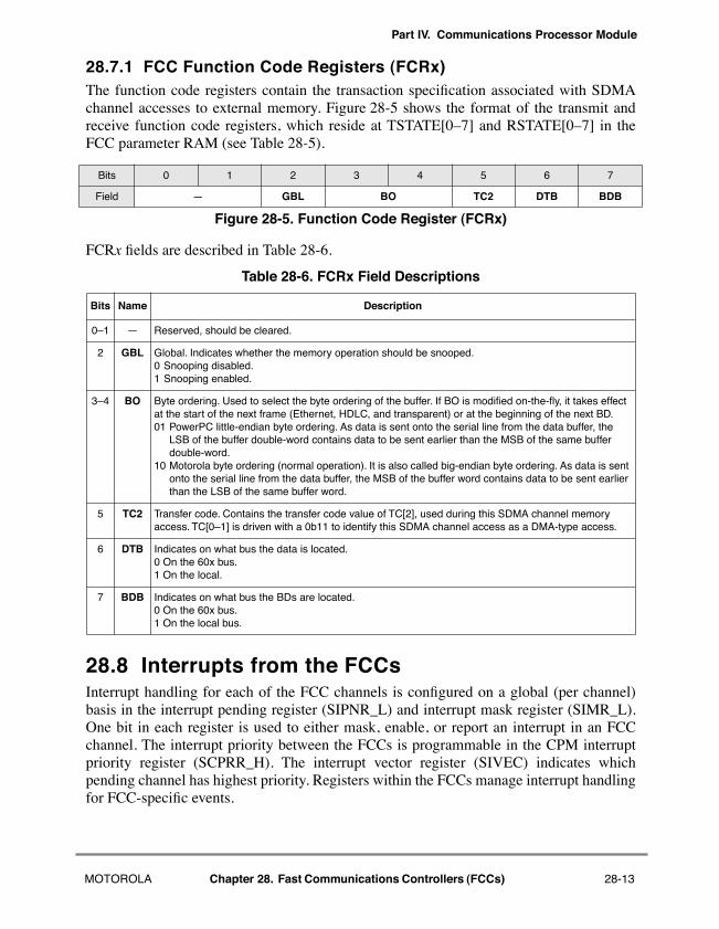
Part IV. Communications Processor Module
28.7.1 FCC Function Code Registers (FCRx)The function code registers contain the transaction speciÞcation associated with SDMAchannel accesses to external memory. Figure 28-5 shows the format of the transmit andreceive function code registers, which reside at TSTATE[0Ð7] and RSTATE[0Ð7] in theFCC parameter RAM (see Table 28-5).
FCRx Þelds are described in Table 28-6.
28.8 Interrupts from the FCCsInterrupt handling for each of the FCC channels is conÞgured on a global (per channel)basis in the interrupt pending register (SIPNR_L) and interrupt mask register (SIMR_L).One bit in each register is used to either mask, enable, or report an interrupt in an FCCchannel. The interrupt priority between the FCCs is programmable in the CPM interruptpriority register (SCPRR_H). The interrupt vector register (SIVEC) indicates whichpending channel has highest priority. Registers within the FCCs manage interrupt handlingfor FCC-speciÞc events.
Bits 0 1 2 3 4 5 6 7
Field Ñ GBL BO TC2 DTB BDB
Figure 28-5. Function Code Register (FCRx)
Table 28-6. FCRx Field Descriptions
Bits Name Description
0Ð1 Ñ Reserved, should be cleared.
2 GBL Global. Indicates whether the memory operation should be snooped. 0 Snooping disabled. 1 Snooping enabled.
3Ð4 BO Byte ordering. Used to select the byte ordering of the buffer. If BO is modiÞed on-the-ßy, it takes effect at the start of the next frame (Ethernet, HDLC, and transparent) or at the beginning of the next BD.01 PowerPC little-endian byte ordering. As data is sent onto the serial line from the data buffer, the
LSB of the buffer double-word contains data to be sent earlier than the MSB of the same buffer double-word.
10 Motorola byte ordering (normal operation). It is also called big-endian byte ordering. As data is sent onto the serial line from the data buffer, the MSB of the buffer word contains data to be sent earlier than the LSB of the same buffer word.
5 TC2 Transfer code. Contains the transfer code value of TC[2], used during this SDMA channel memory access. TC[0Ð1] is driven with a 0b11 to identify this SDMA channel access as a DMA-type access.
6 DTB Indicates on what bus the data is located.0 On the 60x bus.1 On the local.
7 BDB Indicates on what bus the BDs are located.0 On the 60x bus.1 On the local bus.
MOTOROLA Chapter 28. Fast Communications Controllers (FCCs) 28-13
Part IV. Communications Processor Module
Events that can cause the FCC to interrupt the processor vary slightly among protocols andare described with each protocol. These events are handled independently for each channelby the FCC event and mask registers (FCCE and FCCM).
28.8.1 FCC Event Registers (FCCEx)Each FCC has a 24-bit FCC event register (FCCE) used to report events. On recognition ofan event, the FCC sets its corresponding FCCE bit regardless of the corresponding maskbit. To the user it appears as a memory-mapped register that can be read at any time. Bitsare cleared by writing ones; writing zeros has no effect on bit values. FCCE is cleared atreset. Fields of this register are protocol-dependent and are described in the respectiveprotocol sections.
28.8.2 FCC Mask Registers (FCCMx)Each FCC has a 24-bit, read/write FCC mask register (FCCM) used to enable or disable CPinterrupts to the core for events reported in an event register (FCCE). Bit positions inFCCM are identical to those in FCCE. Note that an interrupt is generated only if the FCCinterrupts are also enabled in the SIU; see Section 4.3.1.5, ÒSIU Interrupt Mask Registers(SIMR_H and SIMR_L).Ó
If an FCCM bit is zero, the CP does not proceed with its usual interrupt handling wheneverthat event occurs. Any time a bit in the FCCM register is set, a 1 in the corresponding bit inthe FCCE register sets the FCC event bit in the interrupt pending register; seeSection 4.3.1.4, ÒSIU Interrupt Pending Registers (SIPNR_H and SIPNR_L).Ó
28.8.3 FCC Status Registers (FCCSx)Each FCC has an 8-bit, read/write FCC status register (FCCS) that lets the user monitorreal-time status conditions (ßags, idle) on the RXD line. It does not show the status of CTSand CD; their real-time status is available in the appropriate parallel I/O port (seeChapter 35, ÒParallel I/O PortsÓ).
28.9 FCC InitializationThe FCCs require a number of registers and parameters to be conÞgured after a power-onreset. The following outline gives the proper sequence for initializing the FCCs, regardlessof the protocol used.
1. Write the parallel I/O ports to conÞgure and connect the I/O pins to the FCCs.
2. Write the appropriate port registers to conÞgure CTS and CD to be parallel I/O with interrupt capability or to connect directly to the FCC (if modem support is needed).
3. If the TSA is used, the SI must be conÞgured. If the FCC is used in the NMSI mode, the CPM multiplexing logic (CMX) must still be initialized.
4. Write the GFMR, but do not write the ENT or ENR bits yet.
5. Write the FPSMR.
28-14 MPC8260 PowerQUICC II UserÕs Manual MOTOROLA
Part IV. Communications Processor Module
6. Write the FDSR.
7. Initialize the required values for this FCC in its parameter RAM.
8. Clear out any current events in FCCE, as needed.
9. Write the FCCM register to enable the interrupts in the FCCE register.
10. Write the SCPRR_H to conÞgure the FCC interrupt priority.
11. Clear out any current interrupts in the SIPNR_L, if preferred.
12. Write the SIMR_L to enable interrupts to the CP interrupt controller.
13. Issue an INIT TX AND RX PARAMETERS command (with the correct protocol number).
14. Set GFMR[ENT] and GFMR[ENR].
The Þrst RxBDÕs empty bit must be set before the INIT RX COMMAND. However TxBDs canhave their ready bits set at any time. Notice that the CPCR does not need to be accessedafter a power-on reset until an FCC is to be used. An FCC should be disabled and reenabledafter any dynamic change in its parallel I/O ports or serial channel physical interfaceconÞguration. A full reset using CPCR[RST] is a comprehensive reset that also can be used.
28.10 FCC Interrupt HandlingThe following describes what usually occurs within an FCC interrupt handler:
1. When an interrupt occurs, read FCCE to determine interrupt sources. FCCE bits to be handled in this interrupt handler are normally cleared at this time.
2. Process the TxBDs to reuse them if the FCCE[TX,TXE] were set. If the transmit speed is fast or the interrupt delay is long, more than one transmit buffer may have been sent by the FCC. Thus, it is important to check more than just one TxBD during the interrupt handler. One common practice is to process all TxBDs in the interrupt handler until one is found with R set.
3. Extract data from the RxBD if FCCE[RX, RXB, or RXF] is set. If the receive speed is fast or the interrupt delay is long, the FCC may have received more than one receive buffer. Thus, it is important to check more than just one RxBD during interrupt handling. Typically, all RxBDs in the interrupt handler are processed until one is found with E set. Because the FCC prefetches BDs, the BD table must be big enough such that always there will be another empty BD to prefetch.
4. Clear FCCE.
5. Continue normal execution.
28.11 FCC Timing ControlWhen GFMR[DIAG] is programmed to normal operation, CD and CTS are automaticallycontrolled by the FCC. GFMR[TCI] is assumed to be cleared, which implies normaltransmit clock operation.
MOTOROLA Chapter 28. Fast Communications Controllers (FCCs) 28-15
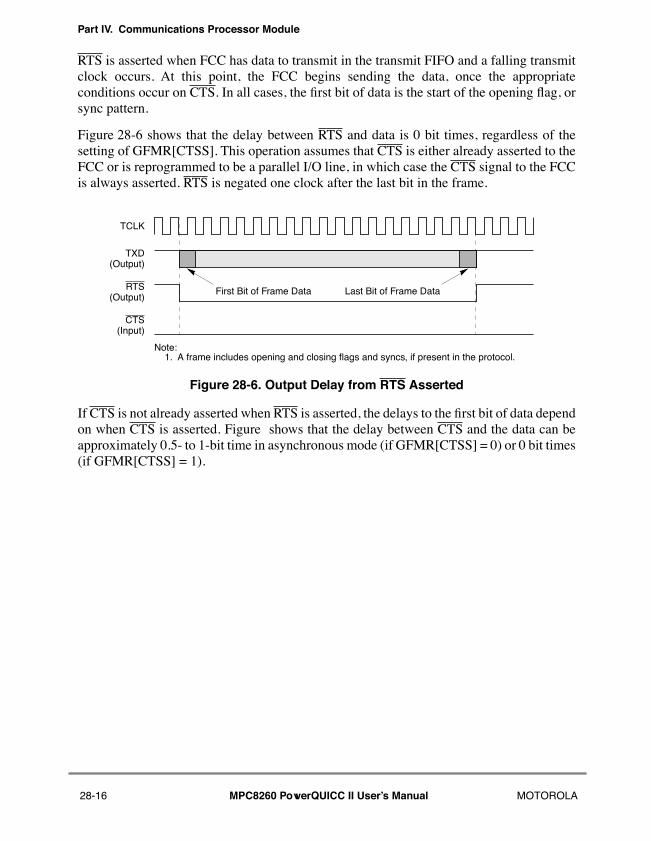
Part IV. Communications Processor Module
RTS is asserted when FCC has data to transmit in the transmit FIFO and a falling transmitclock occurs. At this point, the FCC begins sending the data, once the appropriateconditions occur on CTS. In all cases, the Þrst bit of data is the start of the opening ßag, orsync pattern.
Figure 28-6 shows that the delay between RTS and data is 0 bit times, regardless of thesetting of GFMR[CTSS]. This operation assumes that CTS is either already asserted to theFCC or is reprogrammed to be a parallel I/O line, in which case the CTS signal to the FCCis always asserted. RTS is negated one clock after the last bit in the frame.
Figure 28-6. Output Delay from RTS Asserted
If CTS is not already asserted when RTS is asserted, the delays to the Þrst bit of data dependon when CTS is asserted. Figure shows that the delay between CTS and the data can beapproximately 0.5- to 1-bit time in asynchronous mode (if GFMR[CTSS] = 0) or 0 bit times(if GFMR[CTSS] = 1).
1. A frame includes opening and closing flags and syncs, if present in the protocol.
TCLK
TXD
Last Bit of Frame DataFirst Bit of Frame Data
Note:
(Output)
RTS(Output)
CTS(Input)
28-16 MPC8260 PowerQUICC II UserÕs Manual MOTOROLA
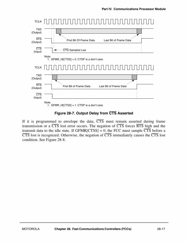
Part IV. Communications Processor Module
Figure 28-7. Output Delay from CTS Asserted
If it is programmed to envelope the data, CTS must remain asserted during frametransmission or a CTS lost error occurs. The negation of CTS forces RTS high and thetransmit data to the idle state. If GFMR[CTSS] = 0, the FCC must sample CTS before aCTS lost is recognized. Otherwise, the negation of CTS immediately causes the CTS lostcondition. See Figure 28-8.
1. GFMR_H[CTSS] = 0. CTSP is a donÕt care.
TCLK
TXD
Last Bit of Frame DataFirst Bit Of Frame Data
Note:
CTS Sampled Low
1. GFMR_H[CTSS] = 1. CTSP is a donÕt care.
TCLK
TXD
Last Bit of Frame DataFirst Bit of Frame Data
Note:
(Output)
RTS(Output)
CTS(Input)
(Output)
RTS(Output)
CTS(Input)
MOTOROLA Chapter 28. Fast Communications Controllers (FCCs) 28-17
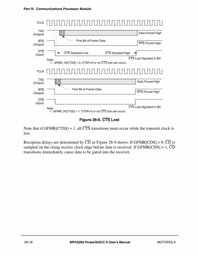
Part IV. Communications Processor Module
Figure 28-8. CTS Lost
Note that if GFMR[CTSS] = 1, all CTS transitions must occur while the transmit clock is low.
Reception delays are determined by CD as Figure 28-9 shows. If GFMR[CDS] = 0, CD issampled on the rising receive clock edge before data is received. If GFMR[CDS] = 1, CDtransitions immediately cause data to be gated into the receiver.
1. GFMR_H[CTSS] = 0. CTSP=0 or no CTS lost can occur.
TCLK
TXD
First Bit of Frame Data
Note:
CTS Sampled Low
1. GFMR_H[CTSS] = 1. CTSP=0 or no CTS lost can occur.
TCLK
First Bit of Frame Data
Note:
CTS Sampled High
Data Forced High
RTS Forced High
Data Forced High
RTS Forced High
CTS Lost Signaled in BD
CTS Lost Signaled in BD
(Output)
RTS(Output)
CTS(Input)
CTS(Input)
RTS(Output)
TXD(Output)
28-18 MPC8260 PowerQUICC II UserÕs Manual MOTOROLA
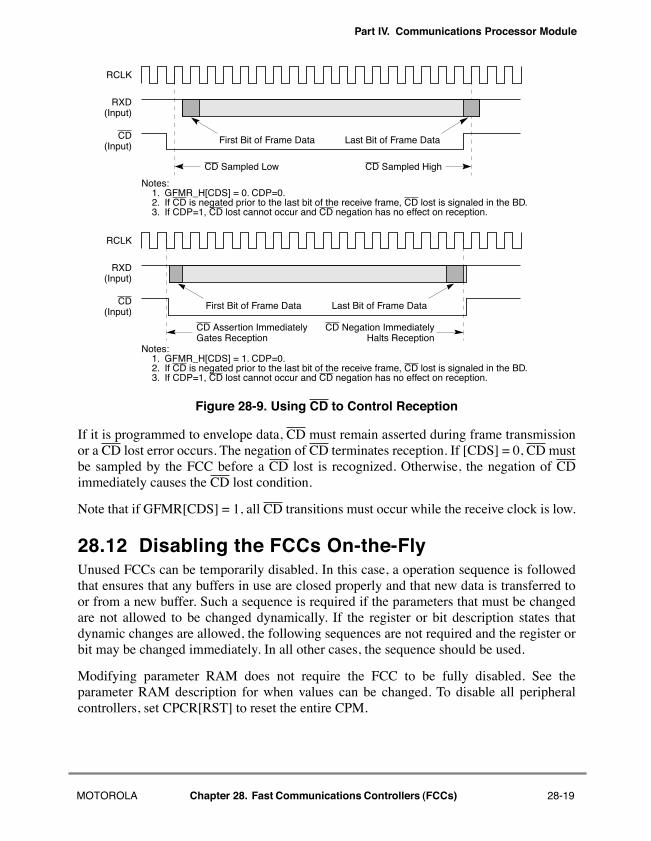
Part IV. Communications Processor Module
Figure 28-9. Using CD to Control Reception
If it is programmed to envelope data, CD must remain asserted during frame transmissionor a CD lost error occurs. The negation of CD terminates reception. If [CDS] = 0, CD mustbe sampled by the FCC before a CD lost is recognized. Otherwise, the negation of CDimmediately causes the CD lost condition.
Note that if GFMR[CDS] = 1, all CD transitions must occur while the receive clock is low.
28.12 Disabling the FCCs On-the-FlyUnused FCCs can be temporarily disabled. In this case, a operation sequence is followedthat ensures that any buffers in use are closed properly and that new data is transferred toor from a new buffer. Such a sequence is required if the parameters that must be changedare not allowed to be changed dynamically. If the register or bit description states thatdynamic changes are allowed, the following sequences are not required and the register orbit may be changed immediately. In all other cases, the sequence should be used.
Modifying parameter RAM does not require the FCC to be fully disabled. See theparameter RAM description for when values can be changed. To disable all peripheralcontrollers, set CPCR[RST] to reset the entire CPM.
1. GFMR_H[CDS] = 0. CDP=0.
RCLK
First Bit of Frame Data
Notes:
CD Sampled Low
RCLK
CD Sampled High
Last Bit of Frame Data
2. If CD is negated prior to the last bit of the receive frame, CD lost is signaled in the BD.3. If CDP=1, CD lost cannot occur and CD negation has no effect on reception.
1. GFMR_H[CDS] = 1. CDP=0.Notes:
2. If CD is negated prior to the last bit of the receive frame, CD lost is signaled in the BD.3. If CDP=1, CD lost cannot occur and CD negation has no effect on reception.
Last Bit of Frame DataFirst Bit of Frame Data
CD Assertion ImmediatelyGates Reception
CD Negation ImmediatelyHalts Reception
RXD(Input)
CD(Input)
CD(Input)
RXD(Input)
MOTOROLA Chapter 28. Fast Communications Controllers (FCCs) 28-19
Part IV. Communications Processor Module
28.12.1 FCC Transmitter Full SequenceFor the FCC transmitter, the full disable and enable sequence is as follows.
1. Issue the STOP TRANSMIT command. This is recommended if the FCC is currently transmitting data because it stops transmission in an orderly way. If the FCC is not transmitting (no TxBDs are ready or the GRACEFUL STOP TRANSMIT command has been issued and completed), then the STOP TRANSMIT command is not required. Furthermore, if the TBPTR is overwritten by the user or the INIT TX PARAMETERS command is executed, this command is not required.
2. Clear GFMR[ENT]. This disables the FCC transmitter and puts it in a reset state.
3. Make changes. The user can modify FCC transmit parameters, including the parameter RAM. To switch protocols or restore the FCC transmit parameters to their initial state, the INIT TX PARAMETERS command must be issued.
4. If an INIT TX PARAMETERS command was not issued in step 3, issue a RESTART TRANSMIT command.
5. Set GFMR[ENT]. Transmission begins using the TxBD that the TBPTR points to as soon as TxBD[R] = 1.
28.12.2 FCC Transmitter Shortcut SequenceA shorter sequence is possible if the user prefers to reinitialize the transmit parameters tothe state they had after reset. This sequence is as follows:
1. Clear GFMR[ENT].
2. Issue the INIT TX PARAMETERS command. Any additional changes can be made now.
3. Set GFMR[ENT].
28.12.3 FCC Receiver Full SequenceThe full disable and enable sequence for the receiver is as follows:
1. Clear GFMR[ENR]. Reception is aborted immediately, which disables the receiver of the FCC and puts it in a reset state.
2. Make changes. The user can modify the FCC receive parameters, including the parameter RAM. If the user prefers to switch protocols or restore the FCC receive parameters to their initial state, the INIT RX PARAMETERS command must be issued.
3. Issue the ENTER HUNT MODE command. This command is required if the INIT RX PARAMETERS command was not issued in step 2.
4. Set GFMR[ENR]. Reception begins immediately using the RxBD that the RBPTR points to if RxBD[E] = 1.
28-20 MPC8260 PowerQUICC II UserÕs Manual MOTOROLA
Part IV. Communications Processor Module
28.12.4 FCC Receiver Shortcut SequenceA shorter sequence is possible if the user prefers to reinitialize the receive parameters to thestate they had after reset. This sequence is as follows:
1. Clear GFMR[ENR].
2. Issue the INIT RX PARAMETERS command. Any additional changes can be made now.
3. Set GFMR[ENR].
28.12.5 Switching ProtocolsA user can switch the protocol that the FCC is executing (HDLC) without resetting theboard or affecting any other FCC by taking the following steps:
1. Clear GFMR[ENT] and GFMR[ENR].
2. Issue the INIT TX AND RX PARAMETERS command. This command initializes both transmit and receive parameters. Additional changes can be made in the GFMR to change the protocol.
3. Set GFMR[ENT] and GFMR[ENR]. The FCC is enabled with the new protocol.
28.13 Saving PowerClearing an FCCÕs ENT and ENR bits minimizes its power consumption.
MOTOROLA Chapter 28. Fast Communications Controllers (FCCs) 28-21
Part IV. Communications Processor Module
28-22 MPC8260 PowerQUICC II UserÕs Manual MOTOROLA
Chapter 29 ATM Controller290290
The ATM controller provides the ATM and AAL layers of the ATM protocol using theuniversal test and operations physical layer (PHY) interface for ATM (UTOPIA level II) forboth master and slave modes. It performs segmentation and reassembly (SAR) functions ofAAL5, AAL1, and AAL0, and most of the common parts of the convergence sublayer (CP-CS) of these protocols.
For each virtual channel (VC), the controllerÕs ATM pace control (APC) unit generates acell transmission rate to implement constant bit rate (CBR), variable bit rate (VBR),available bit rate (ABR), unspeciÞed bit rate (UBR) or UBR+ trafÞc. To regulate VBRtrafÞc, the APC unit performs a continuous-state leaky bucket algorithm. The APC unit alsouses up to eight priority levels to prioritize real-time ATM channels, such as CBR and real-time VBR, over non-real-time ATM channels such as VBR, ABR and UBR.
The ATM controller performs the ATM Forum (UNI-4.0) ABR ßow control. To performfeedback rate adaptation, it supports forward and backward resource management (RM)cell generation and ATM Forum ßoating-point calculation. ABR ßow control isimplemented in hardware and Þrmware (without software intervention) to prevent potentialdelays during backward RM cell processing and feedback rate adaptation.
The MPC8260 supports a special mode for ATM/TDM interworking. The CPM performsautomatic data forwarding between ATM channels and the MCCsÕ TDM channels withoutcore intervention.
The MPC8260 ATM SAR controller applications are as follows:
¥ ATM line card controllers
¥ ATM-to-WAN interworking (frame relay, T1/E1 circuit emulation)
¥ Residential broadband network interface units (NIU) (ATM-to-Ethernet)
¥ High-performance ATM network interface cards (NIC)
¥ Bridges and routers with ATM interface
MOTOROLA Chapter 29. ATM Controller 29-1
Part IV. Communications Processor Module
29.1 FeaturesThe ATM controller has the following features:
¥ Full duplex segmentation and reassembly at 155 Mbps¥ UTOPIA level II master and slave modes 8/16 bit¥ AAL5, AAL1, AAL0 protocols¥ Up to 255 active VCs internally, and up to 64K VCs using external memory¥ TM 4.0 CBR, VBR, UBR, UBR+ trafÞc types¥ VBR type 1 and 2 trafÞc using leaky buckets (GCRA)¥ TM 4.0 ABR ßow control (EFCI and ER)¥ Idle/unassign cells screening/transmission option¥ External and internal rate transmit modes¥ Special mode for ATM-to-TDM or ATM-to-ATM data forwarding¥ CLP and congestion indication marking¥ User-deÞned cells up to 65 bytes¥ Separate Tx and RxBD tables for each virtual channel (VC)¥ Special mode of global free buffer pools for dynamic and efÞcient memory
allocation with early packet discard (EPD) support¥ Interrupt report per channel using four priority interrupt queues¥ Compliant with ATMF UNI 4.0 and ITU speciÞcation¥ AAL5 cell format
Ñ ReassemblyÐ Reassemble PDU directly to external memoryÐ CRC32 checkÐ CLP and congestion reportÐ CPCS_UU, CPI, and length checkÐ Abort message report
Ñ SegmentationÐ Segment PDU directly from external memoryÐ Performs PDU paddingÐ CRC32 generationÐ Automatic last cell markingÐ Automatic CPCS_UU, CPI, and length insertionÐ Abort message option
¥ AAL1 cell formatÑ Reassembly
Ð Reassemble PDU directly to external memoryÐ Support for partially Þlled cells (conÞgurable on a per-VC basis)
MOTOROLA Chapter 29. ATM Controller 29-2
Part IV. Communications Processor Module
Ð Sequence number checkÐ Sequence number protection (CRC-3 and parity) check
Ñ SegmentationÐ Segment PDU directly from external memoryÐ Partially Þlled cells support (conÞgurable on a per-VC basis)Ð Sequence number generationÐ Sequence number protection (CRC-3 and even parity) generation
Ñ Structured AAL1 cell formatÐ Automatic synchronization using the structured pointer during reassemblyÐ Structured pointer generation during segmentation
Ñ Unstructured AAL1 cell formatÐ Clock recovery using external SRTS (synchronous residual time stamp) logic
during reassemblyÐ SRTS generation using external logic during segmentation
¥ AAL0 formatÑ Receive
Ð Whole cell is put in memoryÐ CRC10 pass/fail indication
Ñ TransmitÐ Reads a whole cell from memoryÐ CRC10 insertion option
¥ Support for user-deÞned cellsÑ Support cells up to 65 bytesÑ Extra header insert/load on a per-frame basisÑ Extra header size has byte resolutionÑ Asymmetric cell size for send and receive Ñ HEC octet insertion option
¥ PHYÑ UTOPIA level II supports 8/16 bits 25/50 MHz
Ð Supports UTOPIA master and slave modesÐ Supports cell-level handshakeÐ Supports multiple-PHY polling mode
¥ ATM pace control (APC) unitÑ Peak cell rate pacing on a per-VC basisÑ Peak-and-sustain cell rate pacing using GCRA on a per-VC basisÑ Peak-and-minimum cell rate pacing on a per-VC basisÑ Up to eight priority levelsÑ Fully managed by CP with no host intervention
29-3 MPC8260 PowerQUICC II UserÕs Manual MOTOROLA
Part IV. Communications Processor Module
¥ Available bit rate (ABR)Ñ Performs ATMF UNI 4.0 ABR ßow control on a per-VC basisÑ Automatic forward-RM, backward-RM cells generationÑ Automatic feedback rate adaptationÑ Support for EFCI (explicit forward congestion indication) and ER (explicit rate)Ñ RM cell ßoating-point calculationsÑ Fully managed by CP with no host intervention
¥ Receive address look-up mechanismÑ Two modes of address look-up are supported
Ð External CAMÐ Address compression
¥ OAM (operations and maintenance) cellsÑ OAM Þltering according to PTI Þeld and reserved VCI ÞeldÑ Raw cell queues for transmission and receptionÑ CRC-10 generation/checkÑ Performance monitoring support
Ð Support up to 64 bidirectional block tests simultaneouslyÐ Automatic FMC and BRC cell generation and terminationÐ User transmit cell0+1 countÐ User transmit cell0 countÐ PM cells time stamp insertionÐ Block error detection code (BEDC0+1) generation/checkÐ Total receive cell0+1 countÐ Total receive cell0 count
Ñ Specifying channel code for F5 OAM cells¥ ATM layer statistic gathering on a per PHY basis.
Ñ UTOPIA receiver error cells count (Rx parity error or short/long cells error)Ñ Misinserted cell countÑ CRC-10 error cells count (ABR ßow only)
¥ Memory managementÑ RxBD table per VC with option of global free buffer pool for AAL5Ñ TxBD table per VC
29.2 ATM Controller OverviewThe following sections provide an overview of the transmitter and receiver portions of theATM controller.
MOTOROLA Chapter 29. ATM Controller 29-4
Part IV. Communications Processor Module
29.2.1 Transmitter OverviewBefore the transmitter is enabled, the host must initialize the MPC8260 and create thetransmit data structure, described in Section 29.10, ÒATM Memory Structure.Ó When datais ready for transmission, the host arranges the BD table and writes the pointer of the ÞrstBD in the transmit connection table (TCT). The host issues an ATM TRANSMIT command,which inserts the current channel to the ATM pace control (APC) unit. The APC unitcontrols the ATM trafÞc of the transmitter. It reads the trafÞc parameters of each channeland divides the total bandwidth among them. The APC unit can pace the peak cell rate,peak-and-sustain cell rate (GCRA trafÞc) or peak-and-minimum cell rate trafÞc. The APCimplements up to eight priority levels for servicing real-time channels before non-real-timechannels.
The transmitter ATM cell is 53Ð65 bytes and includes 4 bytes of ATM cell header, a 1-byteHEC, and 48 bytes of payload. The HEC is a constant taken from FDSRx[0Ð15] when usingUTOPIA 16 and from FDSRx[8Ð15] when using UTOPIA 8; see Section 28.4, ÒFCC DataSynchronization Registers (FDSRx).Ó User-deÞned cells (UDC mode) include an extraheader of 1Ð12 bytes with an optional HEC octet. Cell transfers use the UTOPIA level II,cell-level handshake.
Transmission starts when the APC schedules a channel. According to the channel code, theATM controller reads the channelÕs entry in the TCT and opens the Þrst BD fortransmission.
29.2.1.1 AAL5 Transmitter OverviewThe transmitter reads 48 bytes from the external buffer, adds the cell header, and sends thecell through the UTOPIA interface. The transmitter adds any padding needed and appendsthe AAL5 trailer in the last cell of the AAL5 frame. The trailer consists of CPCS-UU+CPI,data length, and CRC-32 as deÞned in ITU I.363. The CPCS-UU+CPI (2-byte entry) canbe speciÞed by the user or optionally cleared by the transmitter; see Section 29.10.2.3,ÒTransmit Connection Table (TCT).Ó The transmitter identiÞes the last cell of the AAL5message by setting the last (L) indication bit in the PTI Þeld of the cell header. An interruptmay be generated to indicate the end of the frame.
When the transmission of the current frame ends and no additional valid buffers are in theBD table, the transmit process ends. The transmitter keeps polling the BD table every timethis channel is scheduled to transmit. In auto-VC-off mode, the APC automaticallydeactivates the current channel when no buffer is ready to transmit. In this case, a new ATM
TRANSMIT command is needed for transmission of the VC to resume. Note that a buffer-not-ready indication during frame transmission aborts the frame transfer.
29.2.1.2 AAL1 Transmitter OverviewThe MPC8260 supports both structured and unstructured AAL1 formats. For theunstructured format, the transmitter reads 47 bytes from the external buffer and inserts theminto the AAL1 user data Þeld. The AAL1 PDU header, which consists of the sequencenumber (SN) and the sequence number protection (SNP) (CRC-3 and parity bit), is
29-5 MPC8260 PowerQUICC II UserÕs Manual MOTOROLA
Part IV. Communications Processor Module
generated and inserted into the cell. The MPC8260 supports synchronous residual timestamp (SRTS) generation using external PLL. If this mode is enabled, the MPC8260 readsthe SRTS code from the external logic and inserts it into four outgoing cells. SeeSection 29.15, ÒSRTS Generation and Clock Recovery Using External Logic.Ó
For the structured format, the transmitter reads 47 or 46 bytes from the external buffer andinserts them into the AAL1 user data Þeld. The CP generates the AAL1 PDU header andinserts it into the cell. The header consists of the SN, SNP, and the structured pointer.
The MPC8260 supports partially Þlled cells conÞgured on a per-VC basis; only valid octetsare copied from the TxBD to the ATM cell. The rest of the cell is Þlled with padding octets.
29.2.1.3 AAL0 Transmitter OverviewNo speciÞc adaptation layer is provided for AAL0. The ATM controller reads a whole cellfrom an external buffer, which always contains exactly one AAL0 cell. The ATM controlleroptionally generates CRC10 on the cell payload and places it at the end of the payload(CRC10 Þeld). AAL0 mode can be used to send OAM cells or AAL3/4 raw cells.
29.2.1.4 Transmit External Rate and Internal Rate ModesThe ATM controller supports the following two rate modes:
¥ External rate modeÑThe total transmission rate is determined by the PHY transmission rate. The FCC sends cells to keep the PHY FIFOs full; the FCC inserts idle/unassign cells to maintain the transmission rate.
¥ Internal rate modeÑThe total transmission rate is determined by the FCC internal rate timers. In this mode, the FCC does not insert idle/unassign cells. The internal rate mechanism is supported for the Þrst four PHY devices (PHY address 00-03). Each PHY has its own FTIRR, described in Section 29.13.4, ÒFCC Transmit Internal Rate Registers (FTIRRx).Ó The FTIRR includes the initial value of the internal rate timer. A cell transmit request is sent when an internal rate timer expires. When using internal rate mode, the user assigns one of the baud-rate generators (BRGs) to clock the four internal rate timers.
29.2.2 Receiver OverviewBefore the receiver is enabled, the host must initialize the MPC8260 and create the receivedata structure described in Section 29.10, ÒATM Memory Structure.Ó The host arranges aBD table for each ATM channel. Buffers for each connection can be statically allocated(that is, each BD in the BD table is associated with a Þxed buffer location) or in the case ofAAL5, can be fetched by the CP from a global free buffer pool. See Section 29.10.5, ÒATMController Buffer Descriptors (BDs).Ó
The receiver ATM cell size is 53-65 bytes. The cell includes: 4 bytes ATM cell header, 1byte HEC, which is ignored, and 48 bytes payload. User-deÞned cells (UDC mode) includean extra header of 1Ð12 bytes with an optional HEC octet. Cell transfers use the UTOPIAlevel II, cell-level handshake.
29-6 MPC8260 PowerQUICC II UserÕs Manual MOTOROLA
Part IV. Communications Processor Module
Reception starts when the PHY asserts the receive cell available signal (RxCLAV) toindicate that the PHY has a complete cell in its receive FIFO. The receiver reads a completecell from the UTOPIA interface and translates the header address (VP/VC) to a channelcode by performing an address look-up. If no matches are found, the cell is discarded andthe user-network interface (UNI) statistics tables are updated. The receiver uses the channelcode to read the channel parameters from the receive connection table (RCT).
29.2.2.1 AAL5 Receiver OverviewThe receiver copies the 48-byte cell payload to the external buffer and calculates CRC-32on the entire CPCS-PDU. When the last AAL5 cell arrives, the receiver checks the length,CRC-32, and CPCS-UU+CPI Þelds and sets the corresponding RxBD status bits. Aninterrupt may be generated to one of the four interrupt queues. The receiver copies the lastcell to memory including the padding and the AAL5 trailer. The CPCS-UU+CPI (16-bitentry) may be read directly from the AAL5 trailer.
The ATM controller monitors the CLP and CNG state of the incoming cells. When themessage is closed, these events set RxBD[CLP] and RxBD[CNG].
When no buffer is ready to receive cells (busy state), the receiver switches to hunt state anddrops all cells associated with the current frame (partial packet discard). The receiver triesto open new buffers for cell reception only after the last cell of the discarded AAL5 framearrives.
29.2.2.2 AAL1 Receiver OverviewThe ATM controller supports both AAL1 structured and unstructured formats. For theunstructured format, 47 octets are copied to the current receive buffer. The AAL1 PDUheader, which consists of the sequence number (SN) and the sequence number protection(SNP) (CRC-3 and parity bit), is checked. The MPC8260 supports SRTS clock recoveryusing an external PLL. In this mode, the MPC8260 tracks the SRTS from the four incomingcells and writes the SRTS code to external logic. See Section 29.15, ÒSRTS Generation andClock Recovery Using External Logic.Ó
In the unstructured format, when the receive process begins, the receiver hunts for the Þrstcell with a valid sequence number (SN Þeld). When one arrives, the receiver leaves the huntstate and starts receiving. If an SN mismatch is detected, the receiver closes the RxBD, setsRxBD[SNE], and switches to hunt state, where it stays until a cell with a valid SN Þeld isreceived.
For the structured format, 47 or 46 octets are copied to the current receive buffer. The AAL1PDU header, which consists of SN and SNP, is checked and the PDU status is written to theBD.
In the structured format, when the receive process begins, the receiver hunts for the Þrst cellwith a valid structured pointer to gain synchronization. When one arrives, the receiverleaves the hunt state and starts receiving. Then the receiver opens a new buffer. Thestructured pointer points to the Þrst octet of the structured block, which then becomes the
29-7 MPC8260 PowerQUICC II UserÕs Manual MOTOROLA
Part IV. Communications Processor Module
Þrst byte of the new buffer. If an SN mismatch is detected, the ATM receiver closes thecurrent RxBD, sets RxBD[SNE], and returns to the hunt state. The receiver then waits fora cell with a valid structured pointer to regain synchronization.
The MPC8260 supports partially Þlled cells conÞgured on a per-VC basis. In this mode, theATM controller copies only the valid octets from the cell user data Þeld to the buffer.
29.2.2.3 AAL0 Receiver OverviewFor AAL0, no speciÞc adaptation layer processing is done. The ATM controller copies thewhole cell to an external buffer. Each buffer contains exactly one AAL0 cell. The ATMcontroller calculates and checks the CRC10 of the cell payload and sets RxBD[CRE] if aCRC error occurs. AAL0 mode can be useful for receiving OAM cells or AAL3/4 raw cells.
29.2.3 Performance MonitoringThe ATM controller supports performance monitoring testing according to ITU I.610.When performance monitoring is enabled, the ATM controller automatically generates andterminates FMCs (forward monitoring cells) and BRCs (backward reporting cells). SeeSection 29.6.6, ÒPerformance Monitoring.Ó
29.2.4 ABR Flow ControlWhen AAL5-ABR is enabled, the ATM controller implements the ATM Forum TM 4.0available-bit-rate ßow. It automatically inserts forward- and backward-RM cells into theuser cells stream and adjusts the transmission rate according to the backwards RM cellfeedback; see Section 29.10.2.2.2, ÒAAL5-ABR Protocol-SpeciÞc RCT.Ó The ABR ßow iscontrolled on a per-VC basis.
29.3 ATM Pace Control (APC) UnitThe ATM pace control (APC) unit schedules the ATM channels for transmitting. Whileperforming this task, the APC unit uses the following parameters:
¥ Frequency (bandwidth) of each ATM channel
¥ ATM trafÞc pacingÑPeak cell rate (PCR), sustain cell rate (SCR), and minimum rate (MCR)
¥ Priority levelÑReal-time channels (CBR or VBR-RT) are scheduled at high-priority levels; non-real-time channels (VBR-NRT, ABR, UBR) are scheduled at low-priority levels. Up to eight priority levels are available.
29.3.1 APC Modes and ATM Service TypesThe ATM Forum (http://www.atmforum.com) deÞnes the service types described inTable 29-1.
29-8 MPC8260 PowerQUICC II UserÕs Manual MOTOROLA

Part IV. Communications Processor Module
For information about cell rate pacing, see Section 29.3.5, ÒATM TrafÞc Type.Ó Forinformation about prioritization, see Section 29.3.6, ÒDetermining the Priority of an ATMChannel.Ó
29.3.2 APC Unit Scheduling MechanismThe APC unit consists of an APC data structure in the dual-port RAM for each PHY and aspecial scheduling algorithm performed by the CP. Each PHYÕs APC data structureincludes three elements: an APC parameter table, an APC priority table, and celltransmission scheduling tables for each priority level. (See Section 29.10.4, ÒAPC DataStructure.Ó)
Each PHYÕs APC parameter table holds parameters that deÞne the priority table location,the number of priority levels, and other APC parameters. The priority table holds pointersthat deÞne the location and size of each priority levelÕs scheduling table.
Each scheduling table is divided into time slots, as shown in Figure 29-1. The userdetermines the number of ATM cells to be sent each time slot (cells per slot). After achannel is sent, it is removed from the current time slot and advanced to a future time slotaccording to the channelÕs assigned trafÞc rate (speciÞed in time slots). The PCR parameterin the TCT, or the SCR or MCR parameters in the TCT extension (TCTE) determine thechannelÕs actual rate.
Table 29-1. ATM Service Types
Service Type Cell Rate PacingReal-Time/
Non-Real-TimeRelative Priority
CBR PCR RT 1 (highest)
VBR-RT PCR, SCR (peak-and-sustain) RT 2
VBR-NRT PCR, SCR (peak-and-sustain) NRT 3
ABR1
1When ABR ßow control is active, the CP automatically adapts the APC parameters PCR, PCR_FRACTION. These parameters function as the channelÕs allowed cell rate (ACR).
PCR NRT 4
UBR+ PCR, MCR (peak-and-minimum) NRT 5
UBR PCR NRT 6 (lowest)
29-9 MPC8260 PowerQUICC II UserÕs Manual MOTOROLA
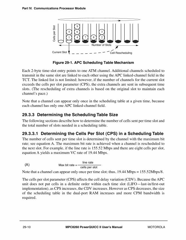
Part IV. Communications Processor Module
Figure 29-1. APC Scheduling Table Mechanism
Each 2-byte time-slot entry points to one ATM channel. Additional channels scheduled totransmit in the same slot are linked to each other using the APC linked-channel Þeld in theTCT. The linked list is not limited; however, if the number of channels for the current slotexceeds the cells per slot parameter (CPS), the extra channels are sent in subsequent timeslots. (The rescheduling of extra channels is based on the original slot to maintain eachchannelÕs pace.)
Note that a channel can appear only once in the scheduling table at a given time, becauseeach channel has only one APC linked-channel Þeld.
29.3.3 Determining the Scheduling Table SizeThe following sections describe how to determine the number of cells sent per time slot andthe total number of slots needed in a scheduling table.
29.3.3.1 Determining the Cells Per Slot (CPS) in a Scheduling TableThe number of cells sent per time slot is determined by the channel with the maximum bitrate; see equation A. The maximum bit rate is achieved when a channel is rescheduled tothe next slot. For example, if the line rate is 155.52 Mbps and there are eight cells per slot,equation A yields a maximum VC rate of 19.44 Mbps.
Note that a channel can appear only once per time slot; thus, 19.44 Mbps = 155.52Mbps/8.
The cells per slot parameter (CPS) affects the cell delay variation (CDV). Because the APCunit does not put cells in a deÞnite order within each time slot (LIFOÑlast-in/Þrst-outimplementation), as CPS increases, the CDV increases. However as CPS decreases, the sizeof the scheduling table in the dual-port RAM increases and more CPM bandwidth isrequired.
1
5
9
4
6
7 8 2
3
Cel
ls p
er S
lot
Number of Slots
Current Slot Cell Rescheduling
Max bit rate = (A)line rate
cells per slot
29-10 MPC8260 PowerQUICC II UserÕs Manual MOTOROLA
Part IV. Communications Processor Module
29.3.3.2 Determining the Number of Slots in a Scheduling TableThe number of time slots in a scheduling table is determined by the channel with theminimum bit rate; see equation B. The minimum bit rate is achieved when the channelreschedules only once in a whole table scan. (The maximum schedule advance allowed isequal to number_of_slots-1.) For example, if the line rate is 155.52 Mbps, the minimum bitrate is 32 kbps and the CPS is 4, then, according to equation B, the number of slots shouldbe 1,216.
For the above example, 32 kbps = 155.52 Mbps/((1216-1) ´ 4).
Use equations (A) and (B) to obtain the maximum and minimum bit rates of a schedulingtable. For example, given a line rate = 155.52 Mbps, number_of_slots = 1025, and CPS = 8:
29.3.4 Determining the Time-Slot Scheduling Rate of a ChannelThe time-slot scheduling rate of each ATM channel is deÞned by equation C. The resultingnumber of APC slots is written in either TCT[PCR], TCTE[SCR] or TCTE[MCR],depending on the trafÞc type.
29.3.5 ATM TrafÞc TypeThe APC uses the cell rate pacing parameters (PCR, SCR, and MCR) to generate CBR,VBR, ABR, UBR+, and UBR trafÞc. The user determines the kind of trafÞc that isgenerated per VC by writing to TCT[ATT] (ATM trafÞc type); see Section 29.10.2.3,ÒTransmit Connection Table (TCT).Ó
29.3.5.1 Peak Cell Rate TrafÞc TypeWhen the peak cell rate trafÞc type is selected, the APC schedules channels to transmitaccording to the PCR and PCR_FRACTION trafÞc parameters. Other trafÞc parameters donot apply to this trafÞc type.
29.3.5.2 Determining the PCR TrafÞc Type ParametersSuppose a VC uses 15.66 Mbps of the total 155.52 Mbps and CPS = 8. Equation C yields:
Min bit rate =(B)(number_of_slots - 1) ´ cells per slot
line rate
Max bit rate = (155.52 Mbps)/8 = 19.44 Mbps
Min bit rate = (155.52 Mbps)/(1024 ´ 8) = 18.98 kbps.
Rate [slots] = (C)VC rate [bps] ´ cells per slot
line rate [bps]
PCR [slots] = (155.52 Mbps)/(15.66 Mbps ´ 8) = 1.241
29-11 MPC8260 PowerQUICC II UserÕs Manual MOTOROLA
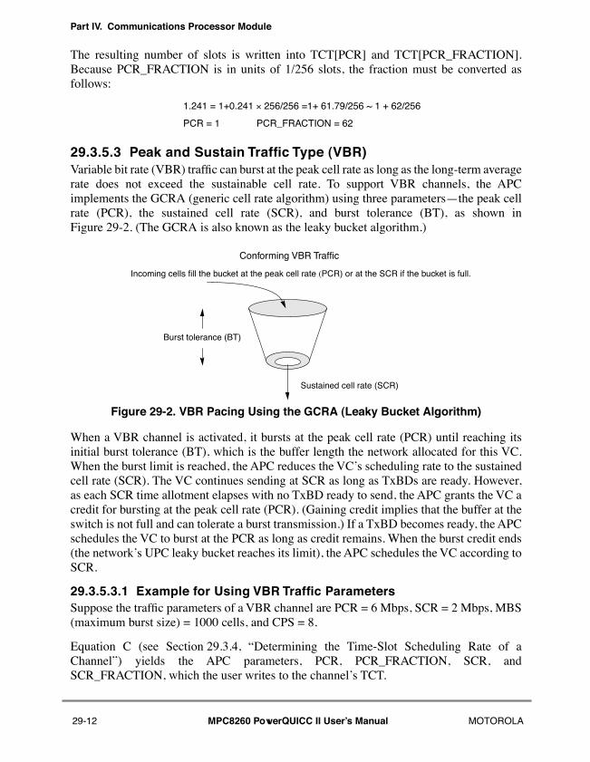
Part IV. Communications Processor Module
The resulting number of slots is written into TCT[PCR] and TCT[PCR_FRACTION].Because PCR_FRACTION is in units of 1/256 slots, the fraction must be converted asfollows:
29.3.5.3 Peak and Sustain TrafÞc Type (VBR)Variable bit rate (VBR) trafÞc can burst at the peak cell rate as long as the long-term averagerate does not exceed the sustainable cell rate. To support VBR channels, the APCimplements the GCRA (generic cell rate algorithm) using three parametersÑthe peak cellrate (PCR), the sustained cell rate (SCR), and burst tolerance (BT), as shown inFigure 29-2. (The GCRA is also known as the leaky bucket algorithm.)
Figure 29-2. VBR Pacing Using the GCRA (Leaky Bucket Algorithm)
When a VBR channel is activated, it bursts at the peak cell rate (PCR) until reaching itsinitial burst tolerance (BT), which is the buffer length the network allocated for this VC.When the burst limit is reached, the APC reduces the VCÕs scheduling rate to the sustainedcell rate (SCR). The VC continues sending at SCR as long as TxBDs are ready. However,as each SCR time allotment elapses with no TxBD ready to send, the APC grants the VC acredit for bursting at the peak cell rate (PCR). (Gaining credit implies that the buffer at theswitch is not full and can tolerate a burst transmission.) If a TxBD becomes ready, the APCschedules the VC to burst at the PCR as long as credit remains. When the burst credit ends(the networkÕs UPC leaky bucket reaches its limit), the APC schedules the VC according toSCR.
29.3.5.3.1 Example for Using VBR TrafÞc ParametersSuppose the trafÞc parameters of a VBR channel are PCR = 6 Mbps, SCR = 2 Mbps, MBS(maximum burst size) = 1000 cells, and CPS = 8.
Equation C (see Section 29.3.4, ÒDetermining the Time-Slot Scheduling Rate of aChannelÓ) yields the APC parameters, PCR, PCR_FRACTION, SCR, andSCR_FRACTION, which the user writes to the channelÕs TCT.
1.241 = 1+0.241 ´ 256/256 =1+ 61.79/256 ~ 1 + 62/256
PCR = 1 PCR_FRACTION = 62
Conforming VBR Traffic
Burst tolerance (BT)
Sustained cell rate (SCR)
Incoming cells fill the bucket at the peak cell rate (PCR) or at the SCR if the bucket is full.
29-12 MPC8260 PowerQUICC II UserÕs Manual MOTOROLA
Part IV. Communications Processor Module
Equation D yields the number of slots the user writes to the channelÕs TCT[BT].
29.3.5.3.2 Handling the Cell Loss Priority (CLP)ÑVBR Type 1 and 2The MPC8260 supports two ways to schedule VBR trafÞc based on the cell loss priority(CLP). When TCTE[VBR2] is cleared, CLP0+1 cells are scheduled by PCR or SCRaccording to the GCRA state. When TCTE[VBR2] is set, CLP0 cells are still scheduled byPCR or SCR according to the GCRA state, but CLP1 cells are always scheduled by PCR.See Section 29.10.2.3.4, ÒVBR Protocol-SpeciÞc TCTE.Ó
29.3.5.4 Peak and Minimum Cell Rate TrafÞc Type (UBR+)To support UBR+ channels, the APC schedules transmission according to PCR and MCR.For each priority level, the APC maintains a parameter that monitors the trafÞc loadmeasured as the time-slot delay between the service pointer (pointing to the current timeslot waiting transmission) and a real-time slot pointer. If the transmission delay is greaterthan MDA (maximum delay allowed), the APC begins scheduling channels according tothe MCR parameter. If the delay, however, drops below MDA, the APC again scheduleschannels according to the PCR. Note that in order to guarantee a minimum cell rate forUBR+ channels, there must be enough bandwidth to simultaneously send all possiblechannels at the MCR. See Section 29.10.2.3.5, ÒUBR+ Protocol-SpeciÞc TCTE.Ó
29.3.6 Determining the Priority of an ATM ChannelThe priority mechanism is implemented by adding priority table levels, which point toseparate scheduling tables; see Section 29.10.4, ÒAPC Data Structure.Ó The APC ßowcontrol services the APC_LEVEL1 slots Þrst. If there are no cells to send, the APC goes tothe next priority level. The APC has up to eight priority levels with APC_LEVEL8 beingthe lowest. The user speciÞes the priority of an ATM channel when issuing the ATM
TRANSMIT command; see Section 29.14, ÒATM Transmit Command.Ó
The real-time channels, CBR and VBR-RT, should be inserted in APC_LEVEL1; non-real-time channels, VBR-NRT, ABR, and UBR should be inserted in lower priority levels.
PCR [slots] = (155.52 Mbps)/(6 Mbps ´ 8) = 3.24
3.24 = 3 + 0.24 ´ 256/256 = 3 + 61.44/256 ~ 3 + 62/256
PCR = 3 PCR_FRACTION = 62
SCR [slots] = (155.52 Mbps)/(2 Mbps ´ 8) = 9.72
9.72 = 9 + (0.72 ´ 256/256) = 9 + 184.32/256 ~ 9 + 185/256
SCR = 9 SCR_FRACTION = 185
BT [slots] = (MBS[cells] - 2) ´ (SCR[slots] - PCR[slots]) + SCR[slots](D)
= (1000 - 2) ´ ((9+185/256) - (3+62/256)) + (9 +185/256)
= 6477
29-13 MPC8260 PowerQUICC II UserÕs Manual MOTOROLA
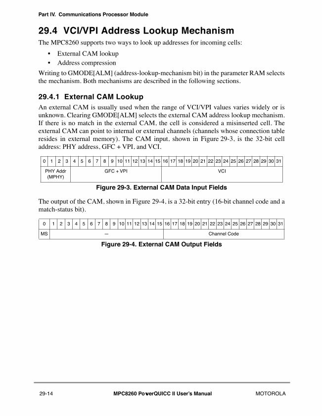
Part IV. Communications Processor Module
29.4 VCI/VPI Address Lookup MechanismThe MPC8260 supports two ways to look up addresses for incoming cells:
¥ External CAM lookup¥ Address compression
Writing to GMODE[ALM] (address-lookup-mechanism bit) in the parameter RAM selectsthe mechanism. Both mechanisms are described in the following sections.
29.4.1 External CAM LookupAn external CAM is usually used when the range of VCI/VPI values varies widely or isunknown. Clearing GMODE[ALM] selects the external CAM address lookup mechanism.If there is no match in the external CAM, the cell is considered a misinserted cell. Theexternal CAM can point to internal or external channels (channels whose connection tableresides in external memory). The CAM input, shown in Figure 29-3, is the 32-bit celladdress: PHY address, GFC + VPI, and VCI.
The output of the CAM, shown in Figure 29-4, is a 32-bit entry (16-bit channel code and amatch-status bit).
0 1 2 3 4 5 6 7 8 9 10 11 12 13 14 15 16 17 18 19 20 21 22 23 24 25 26 27 28 29 30 31
PHY Addr (MPHY)
GFC + VPI VCI
Figure 29-3. External CAM Data Input Fields
0 1 2 3 4 5 6 7 8 9 10 11 12 13 14 15 16 17 18 19 20 21 22 23 24 25 26 27 28 29 30 31
MS Ñ Channel Code
Figure 29-4. External CAM Output Fields
29-14 MPC8260 PowerQUICC II UserÕs Manual MOTOROLA
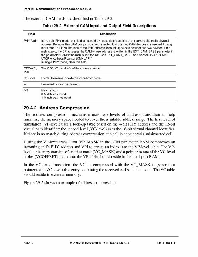
Part IV. Communications Processor Module
The external CAM Þelds are described in Table 29-2
29.4.2 Address CompressionThe address compression mechanism uses two levels of address translation to helpminimize the memory space needed to cover the available address range. The Þrst level oftranslation (VP-level) uses a look-up table based on the 4-bit PHY address and the 12-bitvirtual path identiÞer; the second level (VC-level) uses the 16-bit virtual channel identiÞer.If there is no match during address compression, the cell is considered a misinserted cell.
During the VP-level translation, VP_MASK in the ATM parameter RAM compresses anincoming cellÕs PHY address and VPI to create an index into the VP-level table. The VP-level table entry consists of another mask (VC_MASK) and a pointer to one of the VC-leveltables (VCOFFSET). Note that the VP table should reside in the dual-port RAM.
In the VC-level translation, the VCI is compressed with the VC_MASK to generate apointer to the VC-level table entry containing the received cellÕs channel code. The VC tableshould reside in external memory.
Figure 29-5 shows an example of address compression.
Table 29-2. External CAM Input and Output Field Descriptions
Field Description
PHY Addr In multiple PHY mode, this Þeld contains the 4 least-signiÞcant bits of the current channelÕs physical address. Because this CAM comparison Þeld is limited to 4 bits, two CAM devices are needed if using more than 16 PHYs.The msb of the PHY address lines (bit 4) selects between the two devices. If the msb is zero, the CP accesses the CAM whose address is written in the EXT_CAM_BASE parameter in the parameter RAM; if the msb is set, the CP uses EXT_CAM1_BASE. See Section 15.4.1, ÒCMX UTOPIA Address Register (CMXUAR).ÓIn single PHY mode, clear this Þeld.
GFC+VPI,VCI
The GFC, VPI, and VCI of the current channel.
Ch Code Pointer to internal or external connection table.
Ñ Reserved, should be cleared.
MS Match status.0 Match was found.1 Match was not found.
29-15 MPC8260 PowerQUICC II UserÕs Manual MOTOROLA
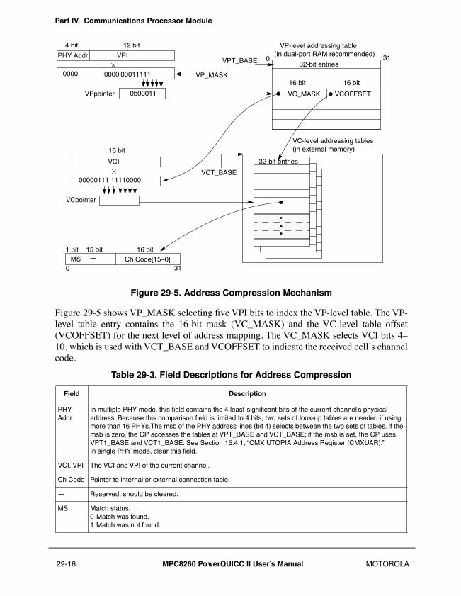
Part IV. Communications Processor Module
Figure 29-5. Address Compression Mechanism
Figure 29-5 shows VP_MASK selecting Þve VPI bits to index the VP-level table. The VP-level table entry contains the 16-bit mask (VC_MASK) and the VC-level table offset(VCOFFSET) for the next level of address mapping. The VC_MASK selects VCI bits 4Ð10, which is used with VCT_BASE and VCOFFSET to indicate the received cellÕs channelcode.
Table 29-3. Field Descriptions for Address Compression
Field Description
PHY Addr
In multiple PHY mode, this Þeld contains the 4 least-signiÞcant bits of the current channelÕs physical address. Because this comparison Þeld is limited to 4 bits, two sets of look-up tables are needed if using more than 16 PHYs.The msb of the PHY address lines (bit 4) selects between the two sets of tables. If the msb is zero, the CP accesses the tables at VPT_BASE and VCT_BASE; if the msb is set, the CP uses VPT1_BASE and VCT1_BASE. See Section 15.4.1, ÒCMX UTOPIA Address Register (CMXUAR).ÓIn single PHY mode, clear this Þeld.
VCI, VPI The VCI and VPI of the current channel.
Ch Code Pointer to internal or external connection table.
Ñ Reserved, should be cleared.
MS Match status.0 Match was found.1 Match was not found.
32-bit entries
VP-level addressing table VPI
0000 00011111
VPpointer
VPT_BASE
VCOFFSETVC_MASK
VCI
00000111 11110000
VCpointer
32-bit entries
VC-level addressing tables
VCT_BASE
VP_MASK16 bit 16 bit
PHY Addr
0000
16 bit
12 bit4 bit
(in external memory)
(in dual-port RAM recommended)
Ch Code[15Ð0]Ñ16 bit15 bit
MS1 bit
310
310
0b00011
29-16 MPC8260 PowerQUICC II UserÕs Manual MOTOROLA
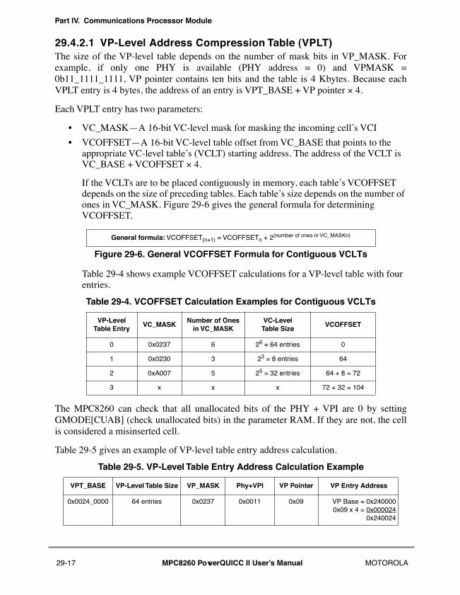
Part IV. Communications Processor Module
29.4.2.1 VP-Level Address Compression Table (VPLT)The size of the VP-level table depends on the number of mask bits in VP_MASK. Forexample, if only one PHY is available (PHY address = 0) and VPMASK =0b11_1111_1111, VP pointer contains ten bits and the table is 4 Kbytes. Because eachVPLT entry is 4 bytes, the address of an entry is VPT_BASE + VP pointer ´ 4.
Each VPLT entry has two parameters:
¥ VC_MASKÑA 16-bit VC-level mask for masking the incoming cellÕs VCI
¥ VCOFFSETÑA 16-bit VC-level table offset from VC_BASE that points to the appropriate VC-level tableÕs (VCLT) starting address. The address of the VCLT is VC_BASE + VCOFFSET ´ 4.
If the VCLTs are to be placed contiguously in memory, each tableÕs VCOFFSET depends on the size of preceding tables. Each tableÕs size depends on the number of ones in VC_MASK. Figure 29-6 gives the general formula for determining VCOFFSET.
Table 29-4 shows example VCOFFSET calculations for a VP-level table with four entries.
The MPC8260 can check that all unallocated bits of the PHY + VPI are 0 by settingGMODE[CUAB] (check unallocated bits) in the parameter RAM. If they are not, the cellis considered a misinserted cell.
Table 29-5 gives an example of VP-level table entry address calculation.
General formula: VCOFFSET(n+1) = VCOFFSETn + 2(number of ones in VC_MASKn)
Figure 29-6. General VCOFFSET Formula for Contiguous VCLTs
Table 29-4. VCOFFSET Calculation Examples for Contiguous VCLTs
VP-Level Table Entry
VC_MASKNumber of Ones
in VC_MASKVC-LevelTable Size
VCOFFSET
0 0x0237 6 26 = 64 entries 0
1 0x0230 3 23 = 8 entries 64
2 0xA007 5 25 = 32 entries 64 + 8 = 72
3 x x x 72 + 32 = 104
Table 29-5. VP-Level Table Entry Address Calculation Example
VPT_BASE VP-Level Table Size VP_MASK Phy+VPI VP Pointer VP Entry Address
0x0024_0000 64 entries 0x0237 0x0011 0x09 VP Base = 0x2400000x09 x 4 = 0x000024
0x240024
29-17 MPC8260 PowerQUICC II UserÕs Manual MOTOROLA
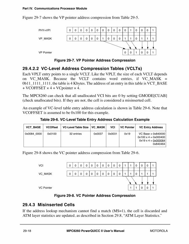
Part IV. Communications Processor Module
Figure 29-7 shows the VP pointer address compression from Table 29-5.
Figure 29-7. VP Pointer Address Compression
29.4.2.2 VC-Level Address Compression Tables (VCLTs)Each VPLT entry points to a single VCLT. Like the VPLT, the size of each VCLT dependson VC_MASK. Because the VCLT contains word entries, if VC_MASK =0b11_1111_1111, the table is 4 Kbytes. The address of an entry in this table is VCT_BASE+ VCOFFSET ´ 4 + VCpointer ´ 4.
The MPC8260 can check that all unallocated VCI bits are 0 by setting GMODE[CUAB](check unallocated bits). If they are not, the cell is considered a misinserted cell.
An example of VC-level table entry address calculation is shown in Table 29-6. Note thatVCOFFSET is assumed to be 0x100 for this example.
Figure 29-8 shows the VC pointer address compression from Table 29-6.
Figure 29-8. VC Pointer Address Compression
29.4.3 Misinserted CellsIf the address lookup mechanism cannot find a match (MS=1), the cell is discarded andATM layer statistics are updated, as described in Section 29.8, ÒATM Layer Statistics.Ó
Table 29-6. VC-Level Table Entry Address Calculation Example
VCT_BASE VCOffset VC-Level Table Size VC_MASK VCI VC Pointer VC Entry Address
0x0084_0000 0x0100 32 entries 0x0037 0x0031 0x19 VC Base = 0x8400000x100 x 4 = 0x0004000x19 x 4 = 0x000064
0x840464
0 0 0 0 0 0 0 1 0 0 0 1
0 0 1 0 0 0 1 1 0 1 1 1
0 0 1
PHY+VPI
VP_MASK
VP Pointer 10
0 0 0 0
0 0 0 0
0
0 0 0 0 0 0 1 1 0 0 0 1
0 0 0 0 0 0 1 1 0 1 1 1
0 0 1
VCI
VC_MASK
VC Pointer 11
0 0 0 0
0 0 0 0
29-18 MPC8260 PowerQUICC II UserÕs Manual MOTOROLA
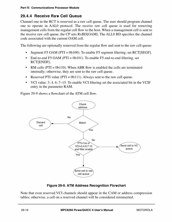
Part IV. Communications Processor Module
29.4.4 Receive Raw Cell QueueChannel one in the RCT is reserved as a raw cell queue. The user should program channelone to operate in AAL0 protocol. The receive raw cell queue is used for removingmanagement cells from the regular cell ßow to the host. When a management cell is sent tothe receive raw cell queue, the CP sets RxBD[OAM]. The ALL0 BD speciÞes the channelcode associated with the current OAM cell.
The following are optionally removed from the regular ßow and sent to the raw cell queue:
¥ Segment F5 OAM (PTI = 0b100). To enable F5 segment Þltering, set RCT[SEGF].
¥ End-to-end F5 OAM (PTI = 0b101). To enable F5 end-to-end Þltering, set RCT[ENDF].
¥ RM cells (PTI = 0b110). When ABR ßow is enabled the cells are terminated internally; otherwise, they are sent to the raw cell queue.
¥ Reserved PTI value (PTI = 0b111). Always sent to the raw cell queue.
¥ VCI value: 3, 4, 6, 7Ð15. To enable VCI Þltering set the associated bit in the VCIF entry in the parameter RAM.
Figure 29-9 shows a ßowchart of the ATM cell ßow.
Figure 29-9. ATM Address Recognition Flowchart
Note that even reserved VCI channels should appear in the CAM or address compressiontables; otherwise, a cell on a reserved channel will be considered misinserted.
NoPTI=1xx or
VCI=3,4,6,7-15and filter enable
Yes
Checkaddress
No
Match
Yes
Discardcell
Send cell to VC queue
Send cell to rawcell queue
29-19 MPC8260 PowerQUICC II UserÕs Manual MOTOROLA
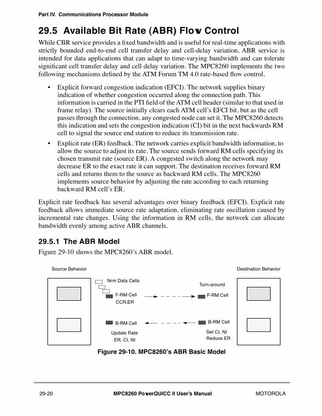
Part IV. Communications Processor Module
29.5 Available Bit Rate (ABR) Flow ControlWhile CBR service provides a Þxed bandwidth and is useful for real-time applications withstrictly bounded end-to-end cell transfer delay and cell-delay variation, ABR service isintended for data applications that can adapt to time-varying bandwidth and can toleratesigniÞcant cell transfer delay and cell delay variation. The MPC8260 implements the twofollowing mechanisms deÞned by the ATM Forum TM 4.0 rate-based ßow control.
¥ Explicit forward congestion indication (EFCI). The network supplies binary indication of whether congestion occurred along the connection path. This information is carried in the PTI Þeld of the ATM cell header (similar to that used in frame relay). The source initially clears each ATM cellÕs EFCI bit, but as the cell passes through the connection, any congested node can set it. The MPC8260 detects this indication and sets the congestion indication (CI) bit in the next backwards RM cell to signal the source end station to reduce its transmission rate.
¥ Explicit rate (ER) feedback. The network carries explicit bandwidth information, to allow the source to adjust its rate. The source sends forward RM cells specifying its chosen transmit rate (source ER). A congested switch along the network may decrease ER to the exact rate it can support. The destination receives forward RM cells and returns them to the source as backward RM cells. The MPC8260 implements source behavior by adjusting the rate according to each returning backward RM cellÕs ER.
Explicit rate feedback has several advantages over binary feedback (EFCI). Explicit ratefeedback allows immediate source rate adaptation, eliminating rate oscillation caused byincremental rate changes. Using the information in RM cells, the network can allocatebandwidth evenly among active ABR channels.
29.5.1 The ABR ModelFigure 29-10 shows the MPC8260Õs ABR model.
Figure 29-10. MPC8260Õs ABR Basic Model
Source Behavior Destination Behavior
Nrm Data Cells
F-RM Cell
B-RM Cell
Update Rate
CCR,ER
ER, CI, NI
F-RM Cell
B-RM Cell
Set CI, NI
Turn-around
Reduce ER
29-20 MPC8260 PowerQUICC II UserÕs Manual MOTOROLA
Part IV. Communications Processor Module
The MPC8260 ABR ßow control implements both source and destination behavior. TheMPC8260Õs ABR ßowchart is described in Section 29.5.1.3, ÒABR Flowcharts.Ó
29.5.1.1 ABR Flow Control Source End-System BehaviorThe MPC8260Õs implementation of ABR ßow control for end-system sources is describedin the following steps:
1. An ABR channelÕs allowed cell rate (ACR) lies between the minimum cell rate (MCR) and the peak cell rate (PCR).
2. ACR is initialized to the initial cell rate (ICR).
3. An F-RM (Forward-RM) cell is sent for every Nrm data cell sent. If more than Mrm cells are sent and the time elapsed since the last F-RM exceeds Trm, an F-RM cell is sent.
4. When sending an F-RM cell, the current ACR is written in the CCR (current cell rate) Þeld of the RM cell.
5. When B-RM (backward-RM) cell is received with CI = 1 (congestion indication), ACR is reduced by ACR ´ RDF (rate decrease factor). After the reduction, the new ACR is determined Þrst by letting ACRtemp be the min of (ACR, ER), and then taking the max of (ACRtemp, MCR).
6. When B-RM is received with CI=0 and NI=0 (no increase), ACR is increased by RIF ´ PCR (rate increase factor). The new ACR is determined Þrst by letting ACRtemp be the min of (ACR, ER), and then taking the max of (ACRtemp, MCR).
7. Before sending an F-RM cell, if more than ADTF (ACR decrease time factor) has elapsed since sending the last F-RM cell, ACR is reduced to ICR. In other words, if the source does not fully use its gained bandwidth, it loses it and resumes sending at its initial cell rate.
8. Before sending an F-RM cell and after action 7, if more than Crm F-RM cells were sent since the last B-RM cell was received with BN=0 (backward notiÞcation), the ACR is reduced by ACR ´ CDF (cutoff decrease factor).
9. A source whose ACR is less than the tag cell rate (TCR) sends out-of-rate cells at the TCR. This behavior is intended for sources whose rates were set to zero by the network. These sources should periodically sense the network state by sending out-of-rate RM cells. In this case data cells will not be sent.
10. An RM cell with an incorrect CRC10 is discarded and the UNI statistics tables are updated.
29.5.1.2 ABR Flow Control Destination End-System BehaviorThe MPC8260Õs implementation of ABR ßow control for end-system destinations isdescribed in the following steps:
1. A received F-RM cell is turned around and sent as a B-RM cells.
2. The DIR Þeld of the received F-RM cell is changed from 0 to 1 (backward DIR).
29-21 MPC8260 PowerQUICC II UserÕs Manual MOTOROLA
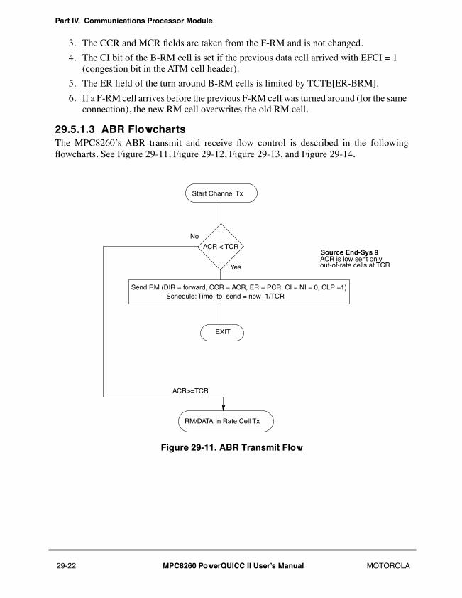
Part IV. Communications Processor Module
3. The CCR and MCR Þelds are taken from the F-RM and is not changed.
4. The CI bit of the B-RM cell is set if the previous data cell arrived with EFCI = 1 (congestion bit in the ATM cell header).
5. The ER Þeld of the turn around B-RM cells is limited by TCTE[ER-BRM].
6. If a F-RM cell arrives before the previous F-RM cell was turned around (for the same connection), the new RM cell overwrites the old RM cell.
29.5.1.3 ABR FlowchartsThe MPC8260Õs ABR transmit and receive flow control is described in the followingßowcharts. See Figure 29-11, Figure 29-12, Figure 29-13, and Figure 29-14.
Figure 29-11. ABR Transmit Flow
Start Channel Tx
ACR < TCR
Send RM (DIR = forward, CCR = ACR, ER = PCR, CI = NI = 0, CLP =1) Schedule: Time_to_send = now+1/TCR
ACR is low sent only
EXIT
RM/DATA In Rate Cell Tx
ACR>=TCR
out-of-rate cells at TCR
Source End-Sys 9
Yes
No
29-22 MPC8260 PowerQUICC II UserÕs Manual MOTOROLA
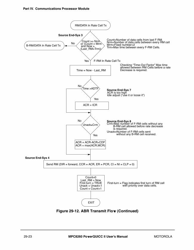
Part IV. Communications Processor Module
Figure 29-12. ABR Transmit Flow (Continued)
RM/DATA In Rate Cell Tx
Count >= Nrmor (Count > Mrmand Now ³ (Last_RM+Trm))
Nrm=Number of data cells between every RM cellMrm=Fixed number=2Trm=Max time between every F-RM Cells.
Count=Number of data cells from last F-RM.
Time = Now - Last_RM
Checking ÒTime-Out FactorÓ Max timeallowed between RM Cells before a rateDecrease is required.
Time >ADTF
ACR = ICR
ACR is too high Idle adjust (Òuse it or loose itÓ)
Unack³Crm
ACR = ACR-ACR´CDFACR = max(ACR,MCR)
Unack=Number of F-RM cells sent without any B-RM cell received.
Crm=Max number of F-RM cells without any B-RM cell allowed before rate decrease is required.
Send RM (DIR = forward, CCR = ACR, ER = PCR, CI = NI = CLP = 0)
Count=0Last_RM = Now
First-turn = TRUEUnack = Unack+1
EXIT
First-turn = Flag indicates first turn of RM cell with priority over data cells.
B-RM/DATA In Rate Cell Tx
F-RM In Rate Cell Tx
Count = Count+1
Source End-Sys 3
Source End-Sys 4
Source End-Sys 7
Source End-Sys 8
Yes
No
Yes
No
Yes
No
29-23 MPC8260 PowerQUICC II UserÕs Manual MOTOROLA
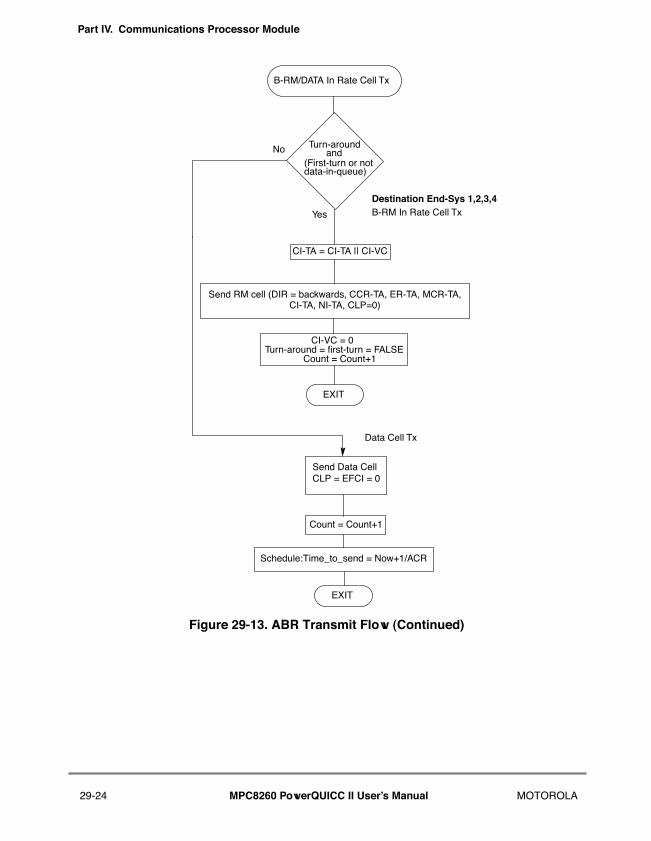
Part IV. Communications Processor Module
Figure 29-13. ABR Transmit Flow (Continued)
B-RM/DATA In Rate Cell Tx
B-RM In Rate Cell Tx
Turn-aroundand
(First-turn or notdata-in-queue)
CI-TA = CI-TA || CI-VC
Send RM cell (DIR = backwards, CCR-TA, ER-TA, MCR-TA,CI-TA, NI-TA, CLP=0)
CI-VC = 0Turn-around = first-turn = FALSE
EXIT
Send Data Cell CLP = EFCI = 0
Count = Count+1
Schedule:Time_to_send = Now+1/ACR
EXIT
Data Cell Tx
Count = Count+1
Destination End-Sys 1,2,3,4
Yes
No
29-24 MPC8260 PowerQUICC II UserÕs Manual MOTOROLA
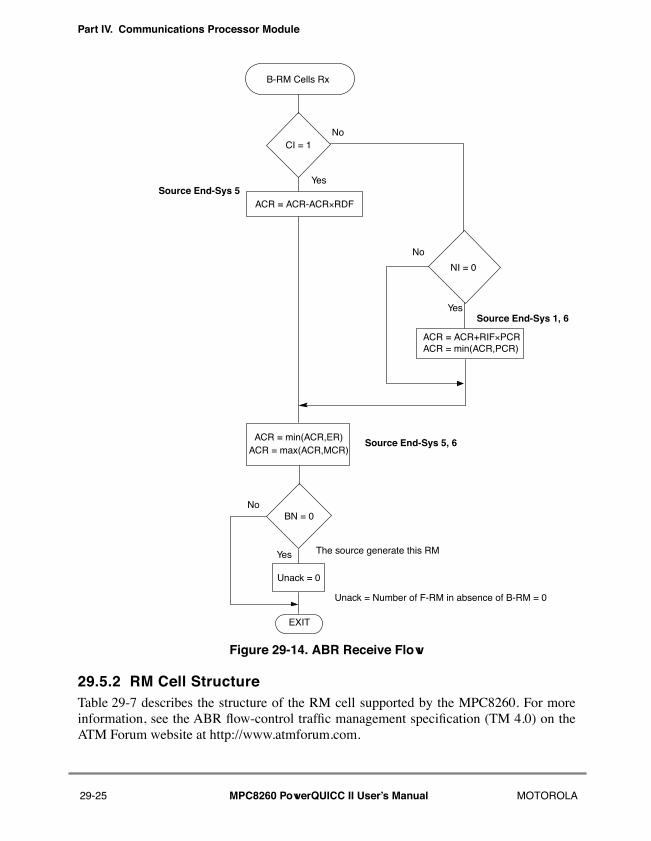
Part IV. Communications Processor Module
Figure 29-14. ABR Receive Flow
29.5.2 RM Cell StructureTable 29-7 describes the structure of the RM cell supported by the MPC8260. For moreinformation, see the ABR ßow-control trafÞc management speciÞcation (TM 4.0) on theATM Forum website at http://www.atmforum.com.
B-RM Cells Rx
CI = 1
ACR = ACR-ACR´RDF
NI = 0
ACR = ACR+RIF´PCRACR = min(ACR,PCR)
ACR = min(ACR,ER)ACR = max(ACR,MCR)
BN = 0
Unack = 0
EXIT
The source generate this RM
Unack = Number of F-RM in absence of B-RM = 0
Source End-Sys 5
Source End-Sys 1, 6
Source End-Sys 5, 6
Yes
No
Yes
No
No
Yes
29-25 MPC8260 PowerQUICC II UserÕs Manual MOTOROLA
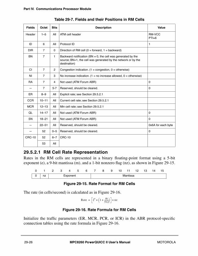
Part IV. Communications Processor Module
29.5.2.1 RM Cell Rate RepresentationRates in the RM cells are represented in a binary ßoating-point format using a 5-bitexponent (e), a 9-bit mantissa (m), and a 1-bit nonzero ßag (nz), as shown in Figure 29-15.
Figure 29-15. Rate Format for RM Cells
The rate (in cells/second) is calculated as in Figure 29-16.
Figure 29-16. Rate Formula for RM Cells
Initialize the trafÞc parameters (ER, MCR, PCR, or ICR) in the ABR protocol-speciÞcconnection tables using the rate formula in Figure 29-16.
Table 29-7. Fields and their Positions in RM Cells
Fields Octet Bits Description Value
Header 1Ð5 All ATM cell header RM-VCCPTI=6
ID 6 All Protocol ID 1
DIR 7 0 Direction of RM cell (0 = forward, 1 = backward)
BN 7 1 Backward notiÞcation (BN = 0, the cell was generated by the source; BN=1, the cell was generated by the network or by the destination)
CI 7 2 Congestion indication. (1 = congestion, 0 = otherwise)
NI 7 3 No increase indication. (1 = no increase allowed, 0 = otherwise)
RA 7 4 Not used (ATM Forum ABR) 0
Ñ 7 5-7 Reserved, should be cleared. 0
ER 8Ð9 All Explicit rate; see Section 29.5.2.1
CCR 10Ð11 All Current cell rate; see Section 29.5.2.1
MCR 12Ð13 All Min cell rate; see Section 29.5.2.1
QL 14Ð17 All Not used (ATM Forum ABR) 0
SN 18Ð21 All Not used (ATM Forum ABR) 0
Ñ 22Ð51 All Reserved, should be cleared. 0x6A for each byte
Ñ 52 0Ð5 Reserved, should be cleared. 0
CRC-10 52 6Ð7 CRC-10
53 All
0 1 2 3 4 5 6 7 8 9 10 11 12 13 14 15
0 nz Exponent Mantissa
Rate 2e
1 m512---------+è ø
æ ö´ nz´=
29-26 MPC8260 PowerQUICC II UserÕs Manual MOTOROLA
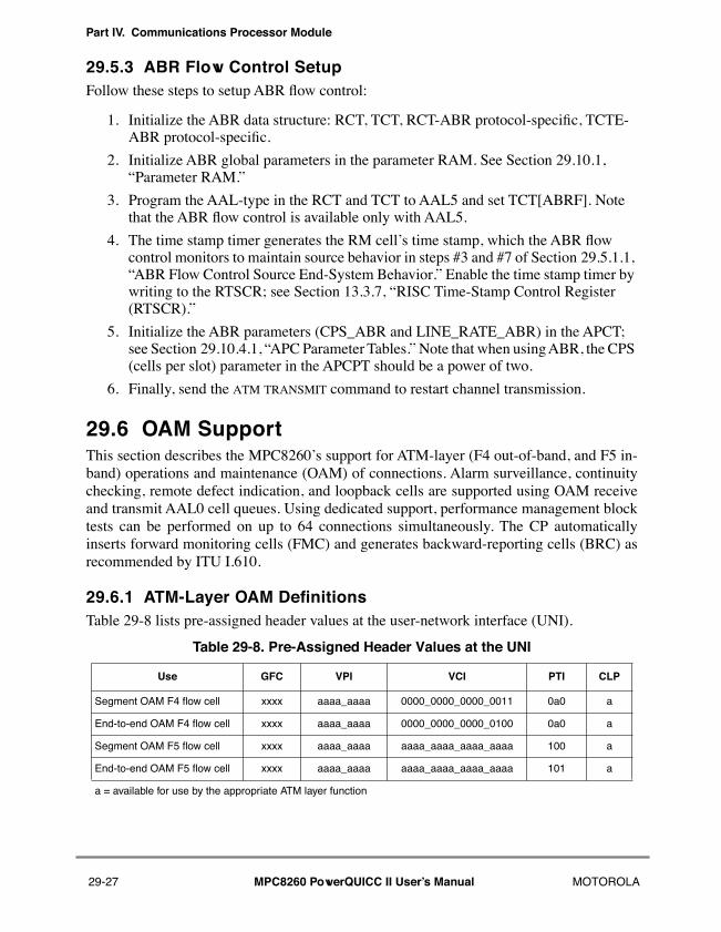
Part IV. Communications Processor Module
29.5.3 ABR Flow Control SetupFollow these steps to setup ABR ßow control:
1. Initialize the ABR data structure: RCT, TCT, RCT-ABR protocol-speciÞc, TCTE-ABR protocol-speciÞc.
2. Initialize ABR global parameters in the parameter RAM. See Section 29.10.1, ÒParameter RAM.Ó
3. Program the AAL-type in the RCT and TCT to AAL5 and set TCT[ABRF]. Note that the ABR ßow control is available only with AAL5.
4. The time stamp timer generates the RM cellÕs time stamp, which the ABR ßow control monitors to maintain source behavior in steps #3 and #7 of Section 29.5.1.1, ÒABR Flow Control Source End-System Behavior.Ó Enable the time stamp timer by writing to the RTSCR; see Section 13.3.7, ÒRISC Time-Stamp Control Register (RTSCR).Ó
5. Initialize the ABR parameters (CPS_ABR and LINE_RATE_ABR) in the APCT; see Section 29.10.4.1, ÒAPC Parameter Tables.Ó Note that when using ABR, the CPS (cells per slot) parameter in the APCPT should be a power of two.
6. Finally, send the ATM TRANSMIT command to restart channel transmission.
29.6 OAM SupportThis section describes the MPC8260Õs support for ATM-layer (F4 out-of-band, and F5 in-band) operations and maintenance (OAM) of connections. Alarm surveillance, continuitychecking, remote defect indication, and loopback cells are supported using OAM receiveand transmit AAL0 cell queues. Using dedicated support, performance management blocktests can be performed on up to 64 connections simultaneously. The CP automaticallyinserts forward monitoring cells (FMC) and generates backward-reporting cells (BRC) asrecommended by ITU I.610.
29.6.1 ATM-Layer OAM DeÞnitionsTable 29-8 lists pre-assigned header values at the user-network interface (UNI).
Table 29-8. Pre-Assigned Header Values at the UNI
Use GFC VPI VCI PTI CLP
Segment OAM F4 ßow cell xxxx aaaa_aaaa 0000_0000_0000_0011 0a0 a
End-to-end OAM F4 ßow cell xxxx aaaa_aaaa 0000_0000_0000_0100 0a0 a
Segment OAM F5 ßow cell xxxx aaaa_aaaa aaaa_aaaa_aaaa_aaaa 100 a
End-to-end OAM F5 ßow cell xxxx aaaa_aaaa aaaa_aaaa_aaaa_aaaa 101 a
a = available for use by the appropriate ATM layer function
29-27 MPC8260 PowerQUICC II UserÕs Manual MOTOROLA
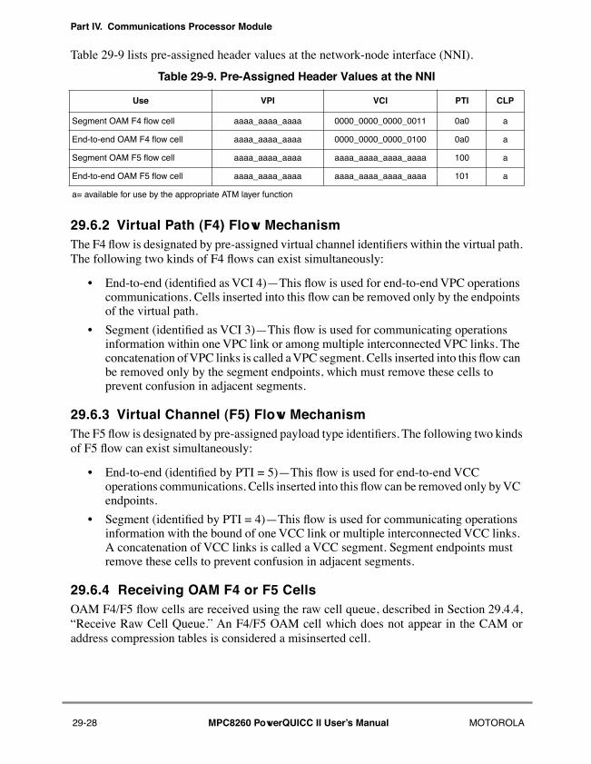
Part IV. Communications Processor Module
Table 29-9 lists pre-assigned header values at the network-node interface (NNI).
29.6.2 Virtual Path (F4) Flow MechanismThe F4 ßow is designated by pre-assigned virtual channel identiÞers within the virtual path.The following two kinds of F4 ßows can exist simultaneously:
¥ End-to-end (identiÞed as VCI 4)ÑThis ßow is used for end-to-end VPC operations communications. Cells inserted into this ßow can be removed only by the endpoints of the virtual path.
¥ Segment (identiÞed as VCI 3)ÑThis ßow is used for communicating operations information within one VPC link or among multiple interconnected VPC links. The concatenation of VPC links is called a VPC segment. Cells inserted into this ßow can be removed only by the segment endpoints, which must remove these cells to prevent confusion in adjacent segments.
29.6.3 Virtual Channel (F5) Flow MechanismThe F5 ßow is designated by pre-assigned payload type identiÞers. The following two kindsof F5 ßow can exist simultaneously:
¥ End-to-end (identiÞed by PTI = 5)ÑThis ßow is used for end-to-end VCC operations communications. Cells inserted into this ßow can be removed only by VC endpoints.
¥ Segment (identiÞed by PTI = 4)ÑThis ßow is used for communicating operations information with the bound of one VCC link or multiple interconnected VCC links. A concatenation of VCC links is called a VCC segment. Segment endpoints must remove these cells to prevent confusion in adjacent segments.
29.6.4 Receiving OAM F4 or F5 CellsOAM F4/F5 ßow cells are received using the raw cell queue, described in Section 29.4.4,ÒReceive Raw Cell Queue.Ó An F4/F5 OAM cell which does not appear in the CAM oraddress compression tables is considered a misinserted cell.
Table 29-9. Pre-Assigned Header Values at the NNI
Use VPI VCI PTI CLP
Segment OAM F4 ßow cell aaaa_aaaa_aaaa 0000_0000_0000_0011 0a0 a
End-to-end OAM F4 ßow cell aaaa_aaaa_aaaa 0000_0000_0000_0100 0a0 a
Segment OAM F5 ßow cell aaaa_aaaa_aaaa aaaa_aaaa_aaaa_aaaa 100 a
End-to-end OAM F5 ßow cell aaaa_aaaa_aaaa aaaa_aaaa_aaaa_aaaa 101 a
a= available for use by the appropriate ATM layer function
29-28 MPC8260 PowerQUICC II UserÕs Manual MOTOROLA
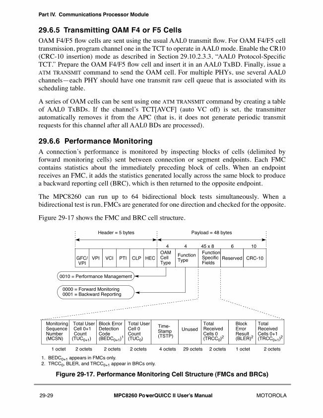
Part IV. Communications Processor Module
29.6.5 Transmitting OAM F4 or F5 CellsOAM F4/F5 ßow cells are sent using the usual AAL0 transmit ßow. For OAM F4/F5 celltransmission, program channel one in the TCT to operate in AAL0 mode. Enable the CR10(CRC-10 insertion) mode as described in Section 29.10.2.3.3, ÒAAL0 Protocol-SpeciÞcTCT.Ó Prepare the OAM F4/F5 ßow cell and insert it in an AAL0 TxBD. Finally, issue aATM TRANSMIT command to send the OAM cell. For multiple PHYs, use several AAL0channelsÑeach PHY should have one transmit raw cell queue that is associated with itsscheduling table.
A series of OAM cells can be sent using one ATM TRANSMIT command by creating a tableof AAL0 TxBDs. If the channelÕs TCT[AVCF] (auto VC off) is set, the transmitterautomatically removes it from the APC (that is, it does not generate periodic transmitrequests for this channel after all AAL0 BDs are processed).
29.6.6 Performance MonitoringA connectionÕs performance is monitored by inspecting blocks of cells (delimited byforward monitoring cells) sent between connection or segment endpoints. Each FMCcontains statistics about the immediately preceding block of cells. When an endpointreceives an FMC, it adds the statistics generated locally across the same block to producea backward reporting cell (BRC), which is then returned to the opposite endpoint.
The MPC8260 can run up to 64 bidirectional block tests simultaneously. When abidirectional test is run, FMCs are generated for one direction and checked for the opposite.
Figure 29-17 shows the FMC and BRC cell structure.
Figure 29-17. Performance Monitoring Cell Structure (FMCs and BRCs)
Header = 5 bytes Payload = 48 bytes
0010 = Performance Management
OAMCellType
FunctionTypeGFC/ VPI VCI PTI CLP HEC
FunctionSpecificFields
ReservedVPI
4 4 645 x 8 10
CRC-10
Unused
2 octets 4 octets 1 octet29 octets 2 octets
Time-Stamp
Total UserCell 0+1
2 octets
Count
1 octet
0000 = Forward Monitoring0001 = Backward Reporting
MonitoringSequenceNumber
BlockErrorResult
TotalReceivedCells 0+1
2 octets
Total UserCell 0Count
2 octets
TotalReceivedCells 0
Block ErrorDetectionCode
(MCSN) (TUC0+1) (BEDC0+1)1 (TUC0) (TSTP) (TRCC0)2 (BLER)2 (TRCC0+1)2
1. BEDC0+1 appears in FMCs only.2. TRCC0, BLER, and TRCC0+1 appear in BRCs only.
29-29 MPC8260 PowerQUICC II UserÕs Manual MOTOROLA

Part IV. Communications Processor Module
Table 29-10 describes performance monitoring cell Þelds.
29.6.6.1 Running a Performance Block TestFor bidirectional PM block tests, FMCs are monitored at the receive side and generated atthe transmit side. The following setup is required to run a bidirectional PM block test on anactive VCC:
1. Assign one of the available 64 performance monitoring tables by writing to both RCT[PMT] and TCT[PMT] and initializing the one chosen. See Section 29.10.3, ÒOAM Performance Monitoring Tables.Ó
2. For PM F5 segment termination set RCT[SEGF]; for PM F5 end-to-end termination set RCT[ENDF].
3. Finally, set the channelÕs RCT[PM] and TCT[PM] and the receive raw cellÕs RCT[PM].
For unidirectional PM block tests:
¥ For PM block monitoring only, set only the RCT Þelds above.
¥ For PM block generation only, set only the TCT Þelds above.
To run a block test on a VPC, assign all the VCCs of the tested VPC to the sameperformance monitoring table. ConÞgure RCT[PMT] and TCT[PMT] to specify theperformance monitoring table associated with each F4 channel.
29.6.6.2 PM Block MonitoringPM block monitoring is done by the receiver. After initialization (see Section 29.6.6.1),whenever a cell is received for a VCC or VPC, the TRCC counters are incremented and the
Table 29-10. Performance Monitoring Cell Fields
Field Description BRC FMC
MCSN Monitoring cell sequence number. The sequence number of the performance monitoring cell (modulo 256).
Yes Yes
TUC0+1 Total user cell 0+1 count. Counts all user cells (modulo 65,536) sent before the FMC was inserted.
Yes Yes
TUC0 Total user cell 0 count. Counts CLP = 0 user cells (modulo 65,536) sent before the FMC was inserted.
Yes Yes
TSTP Time stamp. Used to indicate when the cell was inserted. Yes Yes
BEDC0+1 Block error detection code. Even parity over the payload of the block of user cells sent since the last FMC.
No Yes
TRCC0 Total received cell count 0. Counts CLP=0 user cells (modulo 65,536) received before the FMC was received.
Yes No
BLER Block error result. Counts error parity bits detected by the BEDC of the received FMC. Yes No
TRCC0+1 Total received cell count 0+1. Counts all user cells (modulo 65,536) received before the FMC was received.
Yes No
29-30 MPC8260 PowerQUICC II UserÕs Manual MOTOROLA
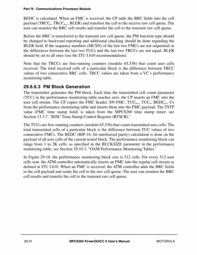
Part IV. Communications Processor Module
BEDC is calculated. When an FMC is received, the CP adds the BRC Þelds into the cellpayload (TRCC0, TRCC0+1, BLER) and transfers the cell to the receive raw cell queue. Theuser can monitor the BRC cell results and transfer the cell to the transmit raw cell queue.
Before the BRC is transferred to the transmit raw cell queue, the PM function type shouldbe changed to backward reporting and additional checking should be done regarding theBLER Þeld. If the sequence numbers (MCSN) of the last two FMCs are not sequential orthe differences between the last two TUCs and the last two TRCCs are not equal, BLERshould be set to all ones (see the ITU I.610 recommendation).
Note that the TRCCs are free-running counters (modulo 65,536) that count user cellsreceived. The total received cells of a particular block is the difference between TRCCvalues of two consecutive BRC cells. TRCC values are taken from a VCÕs performancemonitoring table.
29.6.6.3 PM Block GenerationThe transmitter generates the PM block. Each time the transmitted cell count parameter(TCC) in the performance monitoring table reaches zero, the CP inserts an FMC into theuser cell stream. The CP copies the FMC header, SN-FMC, TUC0+1, TUC0, BEDC0+1-Txfrom the performance monitoring table and inserts them into the FMC payload. The TSTPvalue (FMC time stamp Þeld) is taken from the MPC8260 time stamp timer; seeSection 13.3.7, ÒRISC Time-Stamp Control Register (RTSCR).Ó
The TUCs are free-running counters (modulo 65,536) that count transmitted user cells. Thetotal transmitted cells of a particular block is the difference between TUC values of twoconsecutive FMCs. The BEDC (BIP-16, bit interleaved parity) calculation is done on thepayload of all user cells of the current tested block. The performance monitoring block canrange from 1 to 2K cells, as speciÞed in the BLCKSIZE parameter in the performancemonitoring table; see Section 29.10.3, ÒOAM Performance Monitoring Tables.Ó
In Figure 29-18, the performance monitoring block size is 512 cells. For every 512 usercells sent, the ATM controller automatically inserts an FMC into the regular cell stream asdeÞned in ITU I.610. When an FMC is received, the ATM controller adds the BRC Þeldsto the cell payload and sends the cell to the raw cell queue. The user can monitor the BRCcell results and transfer the cell to the transmit raw cell queue.
29-31 MPC8260 PowerQUICC II UserÕs Manual MOTOROLA
Part IV. Communications Processor Module
Figure 29-18. FMC, BRC Insertion
29.6.6.4 BRC Performance CalculationsBRC reception uses the regular AAL0 raw cell queue. On receiving two consecutive BRCcells, the management layer can calculate the following:
¥ The difference between two TUCs (Nt)
¥ The difference between two TRCCs (Nr)
Information about the connection can be gained by comparing Nt and Nr:
¥ If Nt > Nr, the difference indicates the number of lost cells of this block test.
¥ If Nt < Nr, the difference indicates the number of misinserted cells of this block test.
¥ When Nt = Nr, no cells are lost or misinserted.
29.7 User-DeÞned Cells (UDC)Typical ATM cells are 53 bytes long and consist of a 4-byte header, 1-byte HEC, and 48-byte payload. The MPC8260 also supports user-deÞned cells with up to 12 bytes of extraheader Þelds for internal information for switching applications. This choice is made duringinitialization by writing to the FPSMR; see Section 29.13.2, ÒFCC Protocol-SpeciÞc ModeRegister (FPSMR).Ó As shown in Figure 29-19, the extra header size can vary between 1 to12 bytes (byte resolution) and the HEC octet is optional.
FMC CellData CellData CellFMC CellData CellData CellFMC Cell
512 User Cells512 User Cells
TUC0
Source CellsStream
123
TSTPBEDCTUC0+1
TUC0
TSTPBEDCTUC0+1
TUC0
TSTPBEDCTUC0+1
BRC Cell
TUC0
Destination BRCÕsTransmit Stream
1
TUC0+1
TSTPBLER
TRCC0TRCC0+1
BRC Cell
TUC0
2
TUC0+1
TSTPBLER
TRCC0TRCC0+1
BRC Cell
TUC0
3
TUC0+1
TSTPBLER
TRCC0TRCC0+1
29-32 MPC8260 PowerQUICC II UserÕs Manual MOTOROLA
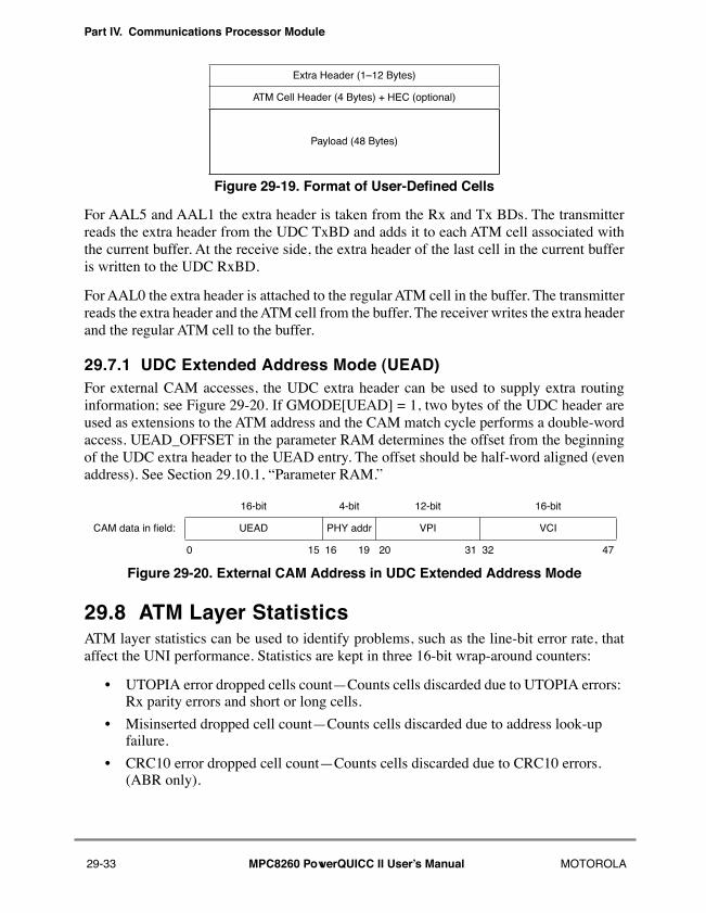
Part IV. Communications Processor Module
For AAL5 and AAL1 the extra header is taken from the Rx and Tx BDs. The transmitterreads the extra header from the UDC TxBD and adds it to each ATM cell associated withthe current buffer. At the receive side, the extra header of the last cell in the current bufferis written to the UDC RxBD.
For AAL0 the extra header is attached to the regular ATM cell in the buffer. The transmitterreads the extra header and the ATM cell from the buffer. The receiver writes the extra headerand the regular ATM cell to the buffer.
29.7.1 UDC Extended Address Mode (UEAD)For external CAM accesses, the UDC extra header can be used to supply extra routinginformation; see Figure 29-20. If GMODE[UEAD] = 1, two bytes of the UDC header areused as extensions to the ATM address and the CAM match cycle performs a double-wordaccess. UEAD_OFFSET in the parameter RAM determines the offset from the beginningof the UDC extra header to the UEAD entry. The offset should be half-word aligned (evenaddress). See Section 29.10.1, ÒParameter RAM.Ó
29.8 ATM Layer StatisticsATM layer statistics can be used to identify problems, such as the line-bit error rate, thataffect the UNI performance. Statistics are kept in three 16-bit wrap-around counters:
¥ UTOPIA error dropped cells countÑCounts cells discarded due to UTOPIA errors: Rx parity errors and short or long cells.
¥ Misinserted dropped cell countÑCounts cells discarded due to address look-up failure.
¥ CRC10 error dropped cell countÑCounts cells discarded due to CRC10 errors. (ABR only).
Extra Header (1Ð12 Bytes)
ATM Cell Header (4 Bytes) + HEC (optional)
Payload (48 Bytes)
Figure 29-19. Format of User-Defined Cells
16-bit 4-bit 12-bit 16-bit
CAM data in Þeld: UEAD PHY addr VPI VCI
0 15 16 19 20 31 32 47
Figure 29-20. External CAM Address in UDC Extended Address Mode
29-33 MPC8260 PowerQUICC II UserÕs Manual MOTOROLA
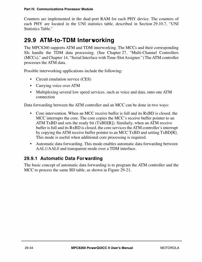
Part IV. Communications Processor Module
Counters are implemented in the dual-port RAM for each PHY device. The counters ofeach PHY are located in the UNI statistics table, described in Section 29.10.7, ÒUNIStatistics Table.Ó
29.9 ATM-to-TDM Interworking The MPC8260 supports ATM and TDM interworking. The MCCs and their correspondingSIs handle the TDM data processing. (See Chapter 27, ÒMulti-Channel Controllers(MCCs),Ó and Chapter 14, ÒSerial Interface with Time-Slot Assigner.Ó) The ATM controllerprocesses the ATM data.
Possible interworking applications include the following:
¥ Circuit emulation service (CES)
¥ Carrying voice over ATM
¥ Multiplexing several low speed services, such as voice and data, onto one ATM connection
Data forwarding between the ATM controller and an MCC can be done in two ways:
¥ Core intervention. When an MCC receive buffer is full and its RxBD is closed, the MCC interrupts the core. The core copies the MCCÕs receive buffer pointer to an ATM TxBD and sets the ready bit (TxBD[R]). Similarly, when an ATM receive buffer is full and its RxBD is closed, the core services the ATM controllerÕs interrupt by copying the ATM receive buffer pointer to an MCC TxBD and setting TxBD[R]. This mode is useful when additional core processing is required.
¥ Automatic data forwarding. This mode enables automatic data forwarding between AAL1/AAL0 and transparent mode over a TDM interface.
29.9.1 Automatic Data ForwardingThe basic concept of automatic data forwarding is to program the ATM controller and theMCC to process the same BD table, as shown in Figure 29-21.
29-34 MPC8260 PowerQUICC II UserÕs Manual MOTOROLA
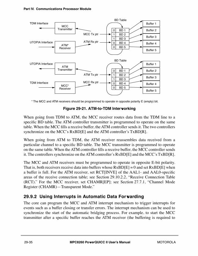
Part IV. Communications Processor Module
Figure 29-21. ATM-to-TDM Interworking
When going from TDM to ATM, the MCC receiver routes data from the TDM line to aspeciÞc BD table. The ATM controller transmitter is programmed to operate on the sametable. When the MCC Þlls a receive buffer, the ATM controller sends it. The two controllerssynchronize on the MCCÕs RxBD[E] and the ATM controllerÕs TxBD[R].
When going from ATM to TDM, the ATM receiver reassembles data received from aparticular channel to a speciÞc BD table. The MCC transmitter is programmed to operateon the same table. When the ATM controller Þlls a receive buffer, the MCC controller sendsit. The controllers synchronize on the ATM controllerÕs RxBD[E] and the MCCÕs TxBD[R].
The MCC and ATM receivers must be programmed to operate in opposite E-bit polarity.That is, both receivers receive data into buffers whose RxBD[E] = 0 and set RxBD[E] whena buffer is full. For the ATM receiver, set RCT[INVE] of the AAL1- and AAL0-speciÞcareas of the receive connection table; see Section 29.10.2.2, ÒReceive Connection Table(RCT).Ó For the MCC receiver, set CHAMR[EP]; see Section 27.7.1, ÒChannel ModeRegister (CHAMR)ÑTransparent Mode.Ó
29.9.2 Using Interrupts in Automatic Data ForwardingThe core can program the MCC and ATM interrupt mechanism to trigger interrupts forevents such as a buffer closing or transfer errors. The interrupt mechanism can be used tosynchronize the start of the automatic bridging process. For example, to start the MCCtransmitter after a speciÞc buffer reaches the ATM receiver (the buffering is required to
MCCTransmitter
TDM Interface Buffer 1
Buffer 2
Buffer 3
Buffer 4
Buffer 5
ATM*Receiver
UTOPIA Interface
BD Table
0 BD 11 BD 21 BD 30 BD 40 BD 5
MCC Tx ptr
ATM Rx ptr
ATMTransmitter
UTOPIA Interface Buffer 1
Buffer 2
Buffer 3
Buffer 4
Buffer 5
MCC*Receiver
TDM Interface
BD Table
0 BD 11 BD 21 BD 30 BD 40 BD 5
ATM Tx ptr
MCC Rx ptr
* The MCC and ATM receivers should be programmed to operate in opposite polarity E (empty) bit.
29-35 MPC8260 PowerQUICC II UserÕs Manual MOTOROLA
Part IV. Communications Processor Module
cope with the ATM networkÕs CDV), set ATM RxBD[I]. When the receive buffer is full, theRxBD is closed, RxBD[E] is set (because it is operating in opposite E-bit polarity), and thecore is interrupted. The core then starts the MCC transmitter.
29.9.3 Timing IssuesUse of the TDM interface assumes that all communicating entities are synchronized (thatis, that they are using a synchronized serial clock). If the TDM interfaces are notsynchronized, a slip can occur in the reassembly buffer. If a buffer-not-ready event occursat the MCC transmitter, the user must restart the MCC transmit channel. If a buffer-not-ready event occurs at the ATM transmitter, the user must restart the ATM transmit channel.
29.9.4 Clock Synchronization (SRTS and Adaptive FIFOs)Clock synchronization methods, such as using a time stamp (SRTS) or adaptive FIFOs,prevent buffer slipping during reassembly. The SRTS method may be implemented usingexternal logic. The MPC8260 can read the SRTS from external logic and insert it intoAAL1 cells, and can track the SRTS from AAL1 cells and deliver it to external logic. SeeSection 29.15, ÒSRTS Generation and Clock Recovery Using External Logic.Ó
Alternatively, an adaptive FIFOs method can be implemented using the core to maintain thebridging buffer at a mid-level point. The difference between the MCC and ATM datapointers is a measure of buffer synchronization. The core calculates the difference betweenpointers at regular intervals and adapts the TDM clock accordingly to hold the differenceconstant.
29.9.5 Mapping TDM Time Slots to VCsUsing the MCC and the SI, any TDM time-slot combination can be routed to a speciÞc databuffer. (See Chapter 27, ÒMulti-Channel Controllers (MCCs),Ó and Chapter 14, ÒSerialInterface with Time-Slot Assigner.Ó) The same data buffers should be used by the ATMcontroller to route receive and transmit data. For information about ATM buffers seeSection 29.10.5, ÒATM Controller Buffer Descriptors (BDs).Ó
29.9.6 CAS SupportFor applications requiring channel-associated signaling (CAS), circuit emulation with CASrequires additional core processing. External framers perform the CAS manipulationthrough a serial or parallel interface.
When the MCC receives a multi-frame block, it generates an interrupt to the core. The corereads the CAS block from the external framer and places it at the end of the ATM data bufferafter the structured multi-frame block. The core then passes the buffer pointer to the ATMcontroller, and the controller packs the data and CAS block into AAL1 cells. All AAL1functions, such as generating PDU-headers and structured pointers, operate normally.
When the ATM controller receives a multi-frame block, it generates an interrupt to the core.The core reads the CAS block from the data buffer and writes it to the external framer. The
29-36 MPC8260 PowerQUICC II UserÕs Manual MOTOROLA
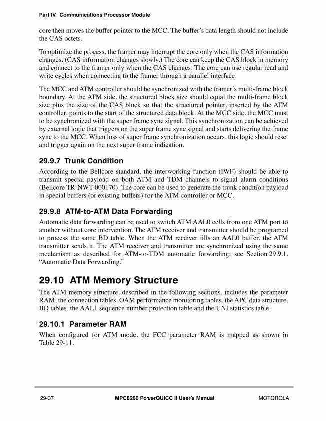
Part IV. Communications Processor Module
core then moves the buffer pointer to the MCC. The bufferÕs data length should not includethe CAS octets.
To optimize the process, the framer may interrupt the core only when the CAS informationchanges. (CAS information changes slowly.) The core can keep the CAS block in memoryand connect to the framer only when the CAS changes. The core can use regular read andwrite cycles when connecting to the framer through a parallel interface.
The MCC and ATM controller should be synchronized with the framerÕs multi-frame blockboundary. At the ATM side, the structured block size should equal the multi-frame blocksize plus the size of the CAS block so that the structured pointer, inserted by the ATMcontroller, points to the start of the structured data block. At the MCC side, the MCC mustto be synchronized with the super frame sync signal. This synchronization can be achievedby external logic that triggers on the super frame sync signal and starts delivering the framesync to the MCC. When loss of super frame synchronization occurs, this logic should resetand trigger again on the next super frame indication.
29.9.7 Trunk ConditionAccording to the Bellcore standard, the interworking function (IWF) should be able totransmit special payload on both ATM and TDM channels to signal alarm conditions(Bellcore TR-NWT-000170). The core can be used to generate the trunk condition payloadin special buffers (or existing buffers) for the ATM controller or MCC.
29.9.8 ATM-to-ATM Data ForwardingAutomatic data forwarding can be used to switch ATM AAL0 cells from one ATM port toanother without core intervention. The ATM receiver and transmitter should be programedto process the same BD table. When the ATM receiver Þlls an AAL0 buffer, the ATMtransmitter sends it. The ATM receiver and transmitter are synchronized using the samemechanism as described for ATM-to-TDM automatic forwarding; see Section 29.9.1,ÒAutomatic Data Forwarding.Ó
29.10 ATM Memory StructureThe ATM memory structure, described in the following sections, includes the parameterRAM, the connection tables, OAM performance monitoring tables, the APC data structure,BD tables, the AAL1 sequence number protection table and the UNI statistics table.
29.10.1 Parameter RAMWhen conÞgured for ATM mode, the FCC parameter RAM is mapped as shown inTable 29-11.
29-37 MPC8260 PowerQUICC II UserÕs Manual MOTOROLA
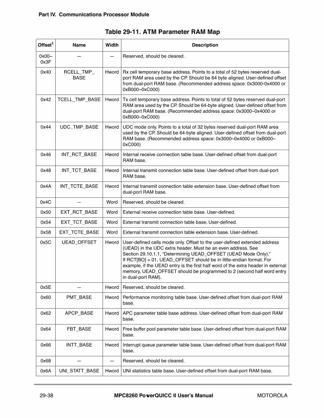
Part IV. Communications Processor Module
Table 29-11. ATM Parameter RAM Map
Offset1 Name Width Description
0x00Ð0x3F
Ñ Ñ Reserved, should be cleared.
0x40 RCELL_TMP_BASE
Hword Rx cell temporary base address. Points to a total of 52 bytes reserved dual-port RAM area used by the CP. Should be 64 byte aligned. User-deÞned offset from dual-port RAM base. (Recommended address space: 0x3000-0x4000 or 0xB000Ð0xC000)
0x42 TCELL_TMP_BASE Hword Tx cell temporary base address. Points to total of 52 bytes reserved dual-port RAM area used by the CP. Should be 64-byte aligned. User-deÞned offset from dual-port RAM base. (Recommended address space: 0x3000Ð0x4000 or 0xB000Ð0xC000)
0x44 UDC_TMP_BASE Hword UDC mode only. Points to a total of 32 bytes reserved dual-port RAM area used by the CP. Should be 64-byte aligned. User-deÞned offset from dual-port RAM base. (Recommended address space: 0x3000Ð0x4000 or 0xB000Ð0xC000)
0x46 INT_RCT_BASE Hword Internal receive connection table base. User-deÞned offset from dual-port RAM base.
0x48 INT_TCT_BASE Hword Internal transmit connection table base. User-deÞned offset from dual-port RAM base.
0x4A INT_TCTE_BASE Hword Internal transmit connection table extension base. User-deÞned offset from dual-port RAM base.
0x4C Ñ Word Reserved, should be cleared.
0x50 EXT_RCT_BASE Word External receive connection table base. User-deÞned.
0x54 EXT_TCT_BASE Word External transmit connection table base. User-deÞned.
0x58 EXT_TCTE_BASE Word External transmit connection table extension base. User-deÞned.
0x5C UEAD_OFFSET Hword User-deÞned cells mode only. Offset to the user-deÞned extended address (UEAD) in the UDC extra header. Must be an even address. See Section 29.10.1.1, ÒDetermining UEAD_OFFSET (UEAD Mode Only).Ó If RCT[BO] = 01, UEAD_OFFSET should be in little-endian format. For example, if the UEAD entry is the Þrst half word of the extra header in external memory, UEAD_OFFSET should be programmed to 2 (second half word entry in dual-port RAM).
0x5E Ñ Hword Reserved, should be cleared.
0x60 PMT_BASE Hword Performance monitoring table base. User-deÞned offset from dual-port RAM base.
0x62 APCP_BASE Hword APC parameter table base address. User-deÞned offset from dual-port RAM base.
0x64 FBT_BASE Hword Free buffer pool parameter table base. User-deÞned offset from dual-port RAM base.
0x66 INTT_BASE Hword Interrupt queue parameter table base. User-deÞned offset from dual-port RAM base.
0x68 Ñ Ñ Reserved, should be cleared.
0x6A UNI_STATT_BASE Hword UNI statistics table base. User-deÞned offset from dual-port RAM base.
29-38 MPC8260 PowerQUICC II UserÕs Manual MOTOROLA
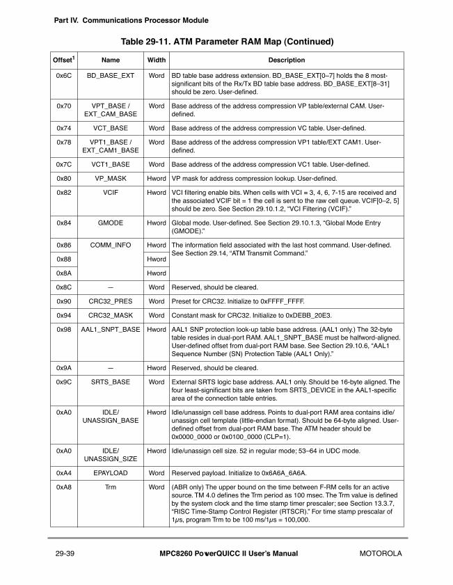
Part IV. Communications Processor Module
0x6C BD_BASE_EXT Word BD table base address extension. BD_BASE_EXT[0Ð7] holds the 8 most-signiÞcant bits of the Rx/Tx BD table base address. BD_BASE_EXT[8Ð31] should be zero. User-deÞned.
0x70 VPT_BASE / EXT_CAM_BASE
Word Base address of the address compression VP table/external CAM. User-deÞned.
0x74 VCT_BASE Word Base address of the address compression VC table. User-deÞned.
0x78 VPT1_BASE / EXT_CAM1_BASE
Word Base address of the address compression VP1 table/EXT CAM1. User-deÞned.
0x7C VCT1_BASE Word Base address of the address compression VC1 table. User-deÞned.
0x80 VP_MASK Hword VP mask for address compression lookup. User-deÞned.
0x82 VCIF Hword VCI Þltering enable bits. When cells with VCI = 3, 4, 6, 7-15 are received and the associated VCIF bit = 1 the cell is sent to the raw cell queue. VCIF[0Ð2, 5] should be zero. See Section 29.10.1.2, ÒVCI Filtering (VCIF).Ó
0x84 GMODE Hword Global mode. User-deÞned. See Section 29.10.1.3, ÒGlobal Mode Entry (GMODE).Ó
0x86 COMM_INFO Hword The information Þeld associated with the last host command. User-deÞned. See Section 29.14, ÒATM Transmit Command.Ó
0x88 Hword
0x8A Hword
0x8C Ñ Word Reserved, should be cleared.
0x90 CRC32_PRES Word Preset for CRC32. Initialize to 0xFFFF_FFFF.
0x94 CRC32_MASK Word Constant mask for CRC32. Initialize to 0xDEBB_20E3.
0x98 AAL1_SNPT_BASE Hword AAL1 SNP protection look-up table base address. (AAL1 only.) The 32-byte table resides in dual-port RAM. AAL1_SNPT_BASE must be halfword-aligned. User-deÞned offset from dual-port RAM base. See Section 29.10.6, ÒAAL1 Sequence Number (SN) Protection Table (AAL1 Only).Ó
0x9A Ñ Hword Reserved, should be cleared.
0x9C SRTS_BASE Word External SRTS logic base address. AAL1 only. Should be 16-byte aligned. The four least-signiÞcant bits are taken from SRTS_DEVICE in the AAL1-speciÞc area of the connection table entries.
0xA0 IDLE/UNASSIGN_BASE
Hword Idle/unassign cell base address. Points to dual-port RAM area contains idle/unassign cell template (little-endian format). Should be 64-byte aligned. User-deÞned offset from dual-port RAM base. The ATM header should be 0x0000_0000 or 0x0100_0000 (CLP=1).
0xA0 IDLE/UNASSIGN_SIZE
Hword Idle/unassign cell size. 52 in regular mode; 53Ð64 in UDC mode.
0xA4 EPAYLOAD Word Reserved payload. Initialize to 0x6A6A_6A6A.
0xA8 Trm Word (ABR only) The upper bound on the time between F-RM cells for an active source. TM 4.0 deÞnes the Trm period as 100 msec. The Trm value is deÞned by the system clock and the time stamp timer prescaler; see Section 13.3.7, ÒRISC Time-Stamp Control Register (RTSCR).Ó For time stamp prescalar of 1µs, program Trm to be 100 ms/1µs = 100,000.
Table 29-11. ATM Parameter RAM Map (Continued)
Offset1 Name Width Description
29-39 MPC8260 PowerQUICC II UserÕs Manual MOTOROLA
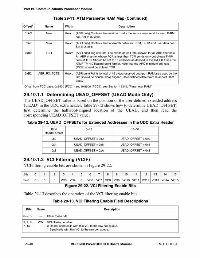
Part IV. Communications Processor Module
29.10.1.1 Determining UEAD_OFFSET (UEAD Mode Only)The UEAD_OFFSET value is based on the position of the user-deÞned extended address(UEAD) in the UDC extra header. Table 29-12 shows how to determine UEAD_OFFSET:Þrst determine the halfword-aligned location of the UEAD, and then read thecorresponding UEAD_OFFSET value.
29.10.1.2 VCI Filtering (VCIF)VCI Þltering enable bits are shown in Figure 29-22.
Table 29-13 describes the operation of the VCI Þltering enable bits.
0xAC Nrm Hword (ABR only) Controls the maximum cells the source may send for each F-RM cell. Set to 32 cells.
0xAE Mrm Hword (ABR only) Controls the bandwidth between F-RM, B-RM and user data cell. Set to 2 cells.
0xB0 TCR Hword (ABR only) Tag cell rate. The minimum cell rate allowed for all ABR channels. An ABR channel whose ACR is less than TCR sends only out-of-rate F-RM cells at TCR. Should be set to 10 cells/sec as deÞned in the TM 4.0. Uses the ATMF TM 4.0 ßoating-point format. Note that the APC minimum cell rate (MCR) should be at least TCR.
0xB2 ABR_RX_TCTE Hword (ABR only) Points to total of 16 bytes reserved dual-port RAM area used by the CP. Should be double-word aligned. User-deÞned offset from dual-port RAM base.
1 Offset from FCC base: 0x8400 (FCC1) and 0x8500 (FCC2); see Section 13.5.2, ÒParameter RAM.Ó
Table 29-12. UEAD_OFFSETs for Extended Addresses in the UDC Extra Header
Bits/Header Offset
0Ð15 16Ð31
0x0 UEAD_OFFSET = 0x2 UEAD_OFFSET = 0x0
0x4 UEAD_OFFSET = 0x6 UEAD_OFFSET = 0x4
0x8 UEAD_OFFSET = 0xA UEAD_OFFSET = 0x8
Bits 0 1 2 3 4 5 6 7 8 9 10 11 12 13 14 15
Field 0 0 0 VC3 VC4 0 VC6 VC7 VC8 VC9 VC10 VC11 VC12 VC13 VC14 VC15
Figure 29-22. VCI Filtering Enable Bits
Table 29-13. VCI Filtering Enable Field Descriptions
Bits Name Description
0Ð2, 5 Ñ Clear these bits.
3, 4, 6,7Ð15
VCx VCI Þltering enable0 Do not send cells with this VCI to the raw cell queue.1 Send cells with this VCI to the raw cell queue.
Table 29-11. ATM Parameter RAM Map (Continued)
Offset1 Name Width Description
29-40 MPC8260 PowerQUICC II UserÕs Manual MOTOROLA
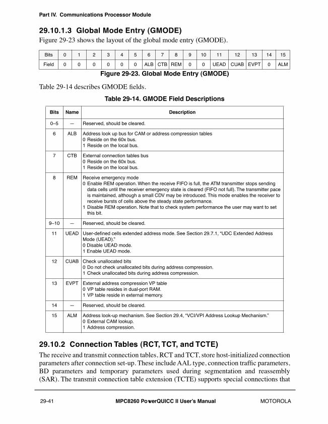
Part IV. Communications Processor Module
29.10.1.3 Global Mode Entry (GMODE)Figure 29-23 shows the layout of the global mode entry (GMODE).
Table 29-14 describes GMODE Þelds.
29.10.2 Connection Tables (RCT, TCT, and TCTE)The receive and transmit connection tables, RCT and TCT, store host-initialized connectionparameters after connection set-up. These include AAL type, connection trafÞc parameters,BD parameters and temporary parameters used during segmentation and reassembly(SAR). The transmit connection table extension (TCTE) supports special connections that
Bits 0 1 2 3 4 5 6 7 8 9 10 11 12 13 14 15
Field 0 0 0 0 0 0 ALB CTB REM 0 0 UEAD CUAB EVPT 0 ALM
Figure 29-23. Global Mode Entry (GMODE)
Table 29-14. GMODE Field Descriptions
Bits Name Description
0Ð5 Ñ Reserved, should be cleared.
6 ALB Address look up bus for CAM or address compression tables0 Reside on the 60x bus.1 Reside on the local bus.
7 CTB External connection tables bus0 Reside on the 60x bus.1 Reside on the local bus.
8 REM Receive emergency mode0 Enable REM operation. When the receive FIFO is full, the ATM transmitter stops sending
data cells until the receiver emergency state is cleared (FIFO not full). The transmitter pace is maintained, although a small CDV may be introduced. This mode enables the receiver to receive bursts of cells above the steady state performance.
1 Disable REM operation. Note that to check system performance the user may want to set this bit.
9Ð10 Ñ Reserved, should be cleared.
11 UEAD User-deÞned cells extended address mode. See Section 29.7.1, ÒUDC Extended Address Mode (UEAD).Ó0 Disable UEAD mode.1 Enable UEAD mode.
12 CUAB Check unallocated bits0 Do not check unallocated bits during address compression.1 Check unallocated bits during address compression.
13 EVPT External address compression VP table0 VP table resides in dual-port RAM.1 VP table reside in external memory.
14 Ñ Reserved, should be cleared.
15 ALM Address look-up mechanism. See Section 29.4, ÒVCI/VPI Address Lookup Mechanism.Ó0 External CAM lookup.1 Address compression.
29-41 MPC8260 PowerQUICC II UserÕs Manual MOTOROLA
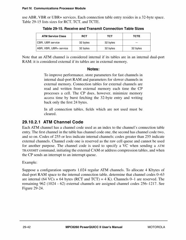
Part IV. Communications Processor Module
use ABR, VBR or UBR+ services. Each connection table entry resides in a 32-byte space.Table 29-15 lists sizes for RCT, TCT, and TCTE.
Note that an ATM channel is considered internal if its tables are in an internal dual-portRAM; it is considered external if its tables are in external memory.
Notes: To improve performance, store parameters for fast channels ininternal dual-port RAM and parameters for slower channels inexternal memory. Connection tables for external channels areread and written from external memory each time the CPprocesses a cell. The CP does, however, minimize memoryaccess time by burst fetching the 32-byte entry and writingback only the Þrst 24 bytes.
In all connection tables, Þelds which are not used must becleared.
29.10.2.1 ATM Channel CodeEach ATM channel has a channel code used as an index to the channelÕs connection tableentry. The Þrst channel in the table has channel code one, the second has channel code two,and so on. Codes of 255 or less indicate internal channels; codes greater than 255 indicateexternal channels. Channel code one is reserved as the raw cell queue and cannot be usedfor another purpose. The channel code is used to specify a VC when sending a ATM
TRANSMIT command, initiating the external CAM or address compression tables, and whenthe CP sends an interrupt to an interrupt queue.
Example:
Suppose a conÞguration supports 1,024 regular ATM channels. To allocate 4 Kbytes ofdual-port RAM space to the internal connection table, determine that channel codes 0Ð63are internal (64 VCs ´ 64 bytes (RCT and TCT) = 4 K). Channels 0Ð1 are reserved. Theremaining 962 (1024 - 62) external channels are assigned channel codes 256Ð1217. SeeFigure 29-24.
Table 29-15. Receive and Transmit Connection Table Sizes
ATM Service Class RCT TCT TCTE
CBR, UBR service 32 bytes 32 bytes Ñ
ABR, VBR, UBR+ service 32 bytes 32 bytes 32 bytes
29-42 MPC8260 PowerQUICC II UserÕs Manual MOTOROLA
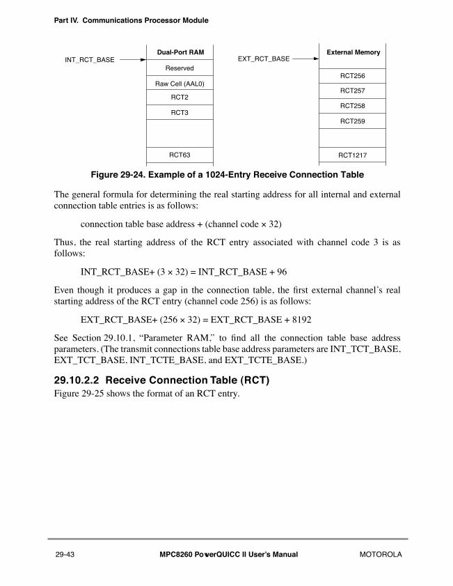
Part IV. Communications Processor Module
Figure 29-24. Example of a 1024-Entry Receive Connection Table
The general formula for determining the real starting address for all internal and externalconnection table entries is as follows:
connection table base address + (channel code ´ 32)
Thus, the real starting address of the RCT entry associated with channel code 3 is asfollows:
INT_RCT_BASE+ (3 ´ 32) = INT_RCT_BASE + 96
Even though it produces a gap in the connection table, the Þrst external channelÕs realstarting address of the RCT entry (channel code 256) is as follows:
EXT_RCT_BASE+ (256 ´ 32) = EXT_RCT_BASE + 8192
See Section 29.10.1, ÒParameter RAM,Ó to Þnd all the connection table base addressparameters. (The transmit connections table base address parameters are INT_TCT_BASE,EXT_TCT_BASE, INT_TCTE_BASE, and EXT_TCTE_BASE.)
29.10.2.2 Receive Connection Table (RCT)Figure 29-25 shows the format of an RCT entry.
Dual-Port RAMINT_RCT_BASE
Reserved
RCT2
RCT3
RCT63
External MemoryEXT_RCT_BASE
RCT256
RCT257
RCT258
RCT259
RCT1217
Raw Cell (AAL0)
29-43 MPC8260 PowerQUICC II UserÕs Manual MOTOROLA
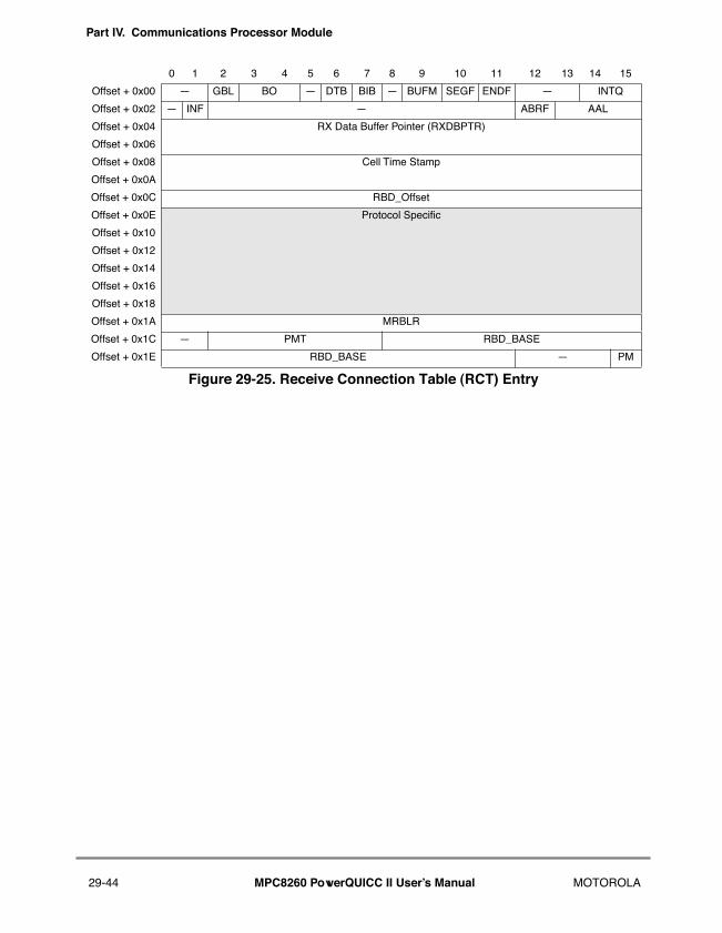
Part IV. Communications Processor Module
0 1 2 3 4 5 6 7 8 9 10 11 12 13 14 15
Offset + 0x00 Ñ GBL BO Ñ DTB BIB Ñ BUFM SEGF ENDF Ñ INTQ
Offset + 0x02 Ñ INF Ñ ABRF AAL
Offset + 0x04 RX Data Buffer Pointer (RXDBPTR)
Offset + 0x06
Offset + 0x08 Cell Time Stamp
Offset + 0x0A
Offset + 0x0C RBD_Offset
Offset + 0x0E Protocol SpeciÞc
Offset + 0x10
Offset + 0x12
Offset + 0x14
Offset + 0x16
Offset + 0x18
Offset + 0x1A MRBLR
Offset + 0x1C Ñ PMT RBD_BASE
Offset + 0x1E RBD_BASE Ñ PM
Figure 29-25. Receive Connection Table (RCT) Entry
29-44 MPC8260 PowerQUICC II UserÕs Manual MOTOROLA
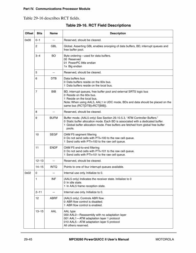
Part IV. Communications Processor Module
Table 29-16 describes RCT Þelds.
Table 29-16. RCT Field Descriptions
Offset Bits Name Description
0x00 0Ð1 Ñ Reserved, should be cleared.
2 GBL Global. Asserting GBL enables snooping of data buffers, BD, interrupt queues and free buffer pool.
3Ð4 BO Byte orderingÑused for data buffers.00 Reserved01 PowerPC little endian1x Big endian
5 Ñ Reserved, should be cleared.
6 DTB Data buffers bus0 Data buffers reside on the 60x bus.1 Data buffers reside on the local bus.
7 BIB BD, interrupt queues, free buffer pool and external SRTS logic bus0 Reside on the 60x bus.1 Reside on the local bus.Note: When using AAL5, AAL1 in UDC mode, BDs and data should be placed on the same bus (RCT[DTB]=RCT[BIB]).
8 Ñ Reserved, should be cleared.
9 BUFM Buffer mode. (AAL5 only) See Section 29.10.5.3, ÒATM Controller Buffers.Ó0 Static buffer allocation mode. Each BD is associated with a dedicated buffer.1 Global buffer allocation mode. Free buffers are fetched from global free buffer
pools.
10 SEGF OAM F5 segment Þltering0 Do not send cells with PTI=100 to the raw cell queue.1 Send cells with PTI=100 to the raw cell queue.
11 ENDF OAM F5 end-to-end Þltering0 Do not send cells with PTI=101 to the raw cell queue.1 Send cells with PTI=101 to the raw cell queue.
12Ð13 Ñ Reserved, should be cleared.
14Ð15 INTQ Points to one of four interrupt queues available.
0x02 0 Ñ Internal use only. Initialize to 0.
1 INF (AAL5 only) Indicates the receiver state. Initialize to 00 In idle state.1 In AAL5 frame reception state.
2Ð11 Ñ Internal use only. Initialize to 0.
12 ABRF (AAL5 only). Controls ABR ßow.0 ABR ßow control is disabled.1 ABR ßow control is enabled.
13Ð15 AAL AAL type000 AAL0ÑReassembly with no adaptation layer001 AAL1ÑATM adaptation layer 1 protocol010 AAL5ÑATM adaptation layer 5 protocolAll others reserved.
29-45 MPC8260 PowerQUICC II UserÕs Manual MOTOROLA
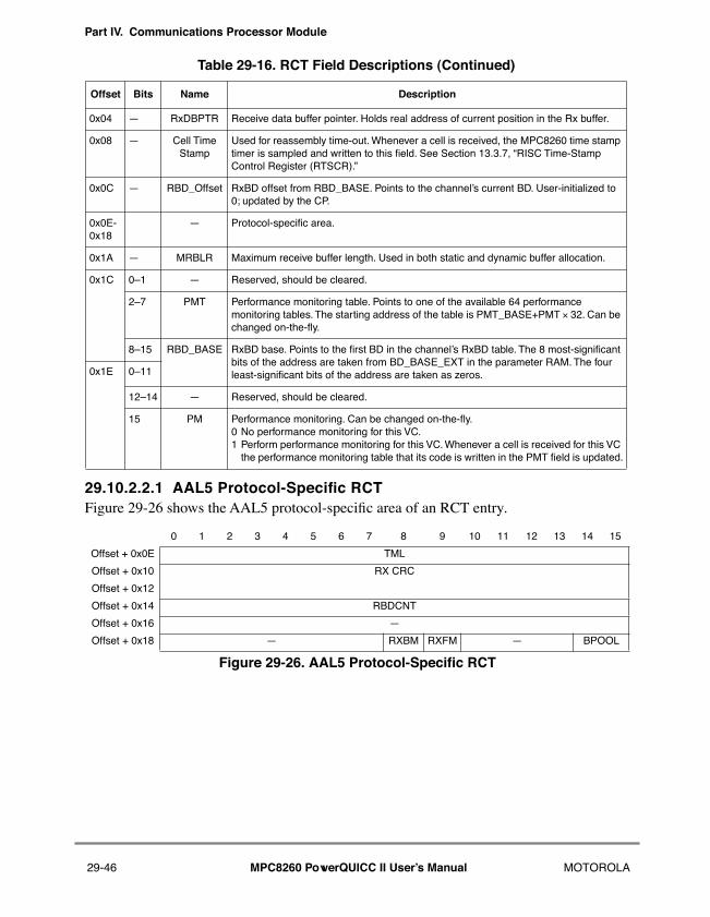
Part IV. Communications Processor Module
29.10.2.2.1 AAL5 Protocol-SpeciÞc RCTFigure 29-26 shows the AAL5 protocol-speciÞc area of an RCT entry.
0x04 Ñ RxDBPTR Receive data buffer pointer. Holds real address of current position in the Rx buffer.
0x08 Ñ Cell Time Stamp
Used for reassembly time-out. Whenever a cell is received, the MPC8260 time stamp timer is sampled and written to this Þeld. See Section 13.3.7, ÒRISC Time-Stamp Control Register (RTSCR).Ó
0x0C Ñ RBD_Offset RxBD offset from RBD_BASE. Points to the channelÕs current BD. User-initialized to 0; updated by the CP.
0x0E-0x18
Ñ Protocol-speciÞc area.
0x1A Ñ MRBLR Maximum receive buffer length. Used in both static and dynamic buffer allocation.
0x1C 0Ð1 Ñ Reserved, should be cleared.
2Ð7 PMT Performance monitoring table. Points to one of the available 64 performance monitoring tables. The starting address of the table is PMT_BASE+PMT ´ 32. Can be changed on-the-ßy.
8Ð15 RBD_BASE RxBD base. Points to the Þrst BD in the channelÕs RxBD table. The 8 most-signiÞcant bits of the address are taken from BD_BASE_EXT in the parameter RAM. The four least-signiÞcant bits of the address are taken as zeros. 0x1E 0Ð11
12Ð14 Ñ Reserved, should be cleared.
15 PM Performance monitoring. Can be changed on-the-ßy.0 No performance monitoring for this VC.1 Perform performance monitoring for this VC. Whenever a cell is received for this VC
the performance monitoring table that its code is written in the PMT Þeld is updated.
0 1 2 3 4 5 6 7 8 9 10 11 12 13 14 15
Offset + 0x0E TML
Offset + 0x10 RX CRC
Offset + 0x12
Offset + 0x14 RBDCNT
Offset + 0x16 Ñ
Offset + 0x18 Ñ RXBM RXFM Ñ BPOOL
Figure 29-26. AAL5 Protocol-Specific RCT
Table 29-16. RCT Field Descriptions (Continued)
Offset Bits Name Description
29-46 MPC8260 PowerQUICC II UserÕs Manual MOTOROLA
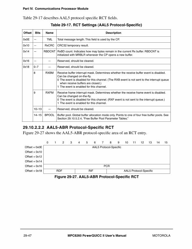
Part IV. Communications Processor Module
Table 29-17 describes AAL5 protocol speciÞc RCT Þelds.
29.10.2.2.2 AAL5-ABR Protocol-SpeciÞc RCTFigure 29-27 shows the AAL5-ABR protocol-speciÞc area of an RCT entry.
Table 29-17. RCT Settings (AAL5 Protocol-Specific)
Offset Bits Name Description
0x0E Ñ TML Total message length. This Þeld is used by the CP.
0x10 Ñ RxCRC CRC32 temporary result.
0x14 Ñ RBDCNT RxBD count. Indicates how may bytes remain in the current Rx buffer. RBDCNT is initialized with MRBLR whenever the CP opens a new buffer.
0x16 Ñ Ñ Reserved, should be cleared.
0x18 0Ð7 Ñ Reserved, should be cleared.
8 RXBM Receive buffer interrupt mask. Determines whether the receive buffer event is disabled. Can be changed on-the-ßy.0 The event is disabled for this channel. (The RXB event is not sent to the interrupt queue
when receive buffers are closed.)1 The event is enabled for this channel.
9 RXFM Receive frame interrupt mask. Determines whether the receive frame event is disabled. Can be changed on-the-ßy.0 The event is disabled for this channel. (RXF event is not sent to the interrupt queue.)1 The event is enabled for this channel.
10Ð13 Ñ Reserved, should be cleared.
14Ð15 BPOOL Buffer pool. Global buffer allocation mode only. Points to one of four free buffer pools. See Section 29.10.5.2.4, ÒFree Buffer Pool Parameter Tables.Ó
0 1 2 3 4 5 6 7 8 9 10 11 12 13 14 15
Offset + 0x0E AAL5 Protocol-SpeciÞc
Offset + 0x10
Offset + 0x12
Offset + 0x14
Offset + 0x16 PCR
Offset + 0x18 RDF RIF AAL5 Protocol-SpeciÞc
Figure 29-27. AAL5-ABR Protocol-Specific RCT
29-47 MPC8260 PowerQUICC II UserÕs Manual MOTOROLA
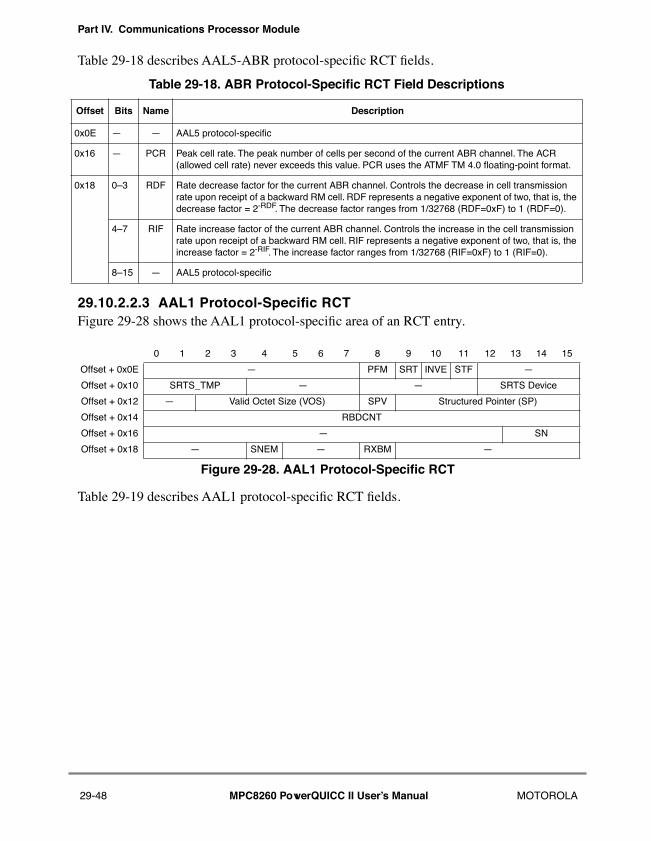
Part IV. Communications Processor Module
Table 29-18 describes AAL5-ABR protocol-speciÞc RCT Þelds.
29.10.2.2.3 AAL1 Protocol-SpeciÞc RCTFigure 29-28 shows the AAL1 protocol-speciÞc area of an RCT entry.
Table 29-19 describes AAL1 protocol-speciÞc RCT Þelds.
Table 29-18. ABR Protocol-Specific RCT Field Descriptions
Offset Bits Name Description
0x0E Ñ Ñ AAL5 protocol-speciÞc
0x16 Ñ PCR Peak cell rate. The peak number of cells per second of the current ABR channel. The ACR (allowed cell rate) never exceeds this value. PCR uses the ATMF TM 4.0 ßoating-point format.
0x18 0Ð3 RDF Rate decrease factor for the current ABR channel. Controls the decrease in cell transmission rate upon receipt of a backward RM cell. RDF represents a negative exponent of two, that is, the decrease factor = 2-RDF. The decrease factor ranges from 1/32768 (RDF=0xF) to 1 (RDF=0).
4Ð7 RIF Rate increase factor of the current ABR channel. Controls the increase in the cell transmission rate upon receipt of a backward RM cell. RIF represents a negative exponent of two, that is, the increase factor = 2-RIF. The increase factor ranges from 1/32768 (RIF=0xF) to 1 (RIF=0).
8Ð15 Ñ AAL5 protocol-speciÞc
0 1 2 3 4 5 6 7 8 9 10 11 12 13 14 15
Offset + 0x0E Ñ PFM SRT INVE STF Ñ
Offset + 0x10 SRTS_TMP Ñ Ñ SRTS Device
Offset + 0x12 Ñ Valid Octet Size (VOS) SPV Structured Pointer (SP)
Offset + 0x14 RBDCNT
Offset + 0x16 Ñ SN
Offset + 0x18 Ñ SNEM Ñ RXBM Ñ
Figure 29-28. AAL1 Protocol-Specific RCT
29-48 MPC8260 PowerQUICC II UserÕs Manual MOTOROLA
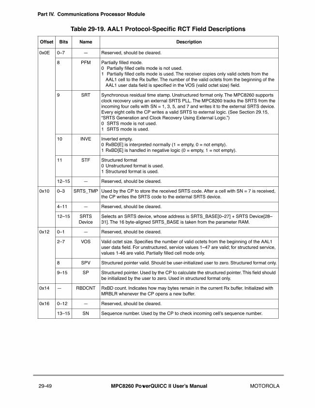
Part IV. Communications Processor Module
Table 29-19. AAL1 Protocol-Specific RCT Field Descriptions
Offset Bits Name Description
0x0E 0Ð7 Ñ Reserved, should be cleared.
8 PFM Partially Þlled mode. 0 Partially Þlled cells mode is not used.1 Partially Þlled cells mode is used. The receiver copies only valid octets from the
AAL1 cell to the Rx buffer. The number of the valid octets from the beginning of the AAL1 user data Þeld is speciÞed in the VOS (valid octet size) Þeld.
9 SRT Synchronous residual time stamp. Unstructured format only. The MPC8260 supports clock recovery using an external SRTS PLL. The MPC8260 tracks the SRTS from the incoming four cells with SN = 1, 3, 5, and 7 and writes it to the external SRTS device. Every eight cells the CP writes a valid SRTS to external logic. (See Section 29.15, ÒSRTS Generation and Clock Recovery Using External Logic.Ó)0 SRTS mode is not used.1 SRTS mode is used.
10 INVE Inverted empty. 0 RxBD[E] is interpreted normally (1 = empty, 0 = not empty).1 RxBD[E] is handled in negative logic (0 = empty, 1 = not empty).
11 STF Structured format0 Unstructured format is used.1 Structured format is used.
12Ð15 Ñ Reserved, should be cleared.
0x10 0Ð3 SRTS_TMP Used by the CP to store the received SRTS code. After a cell with SN = 7 is received, the CP writes the SRTS code to the external SRTS device.
4Ð11 Ñ Reserved, should be cleared.
12Ð15 SRTS Device
Selects an SRTS device, whose address is SRTS_BASE[0Ð27] + SRTS Device[28Ð31]. The 16 byte-aligned SRTS_BASE is taken from the parameter RAM.
0x12 0Ð1 Ñ Reserved, should be cleared.
2Ð7 VOS Valid octet size. SpeciÞes the number of valid octets from the beginning of the AAL1 user data Þeld. For unstructured, service values 1Ð47 are valid; for structured service, values 1-46 are valid. Partially Þlled cell mode only.
8 SPV Structured pointer valid. Should be user-initialized user to zero. Structured format only.
9Ð15 SP Structured pointer. Used by the CP to calculate the structured pointer. This Þeld should be initialized by the user to zero. Used in structured format only.
0x14 Ñ RBDCNT RxBD count. Indicates how may bytes remain in the current Rx buffer. Initialized with MRBLR whenever the CP opens a new buffer.
0x16 0Ð12 Ñ Reserved, should be cleared.
13Ð15 SN Sequence number. Used by the CP to check incoming cellÕs sequence number.
29-49 MPC8260 PowerQUICC II UserÕs Manual MOTOROLA
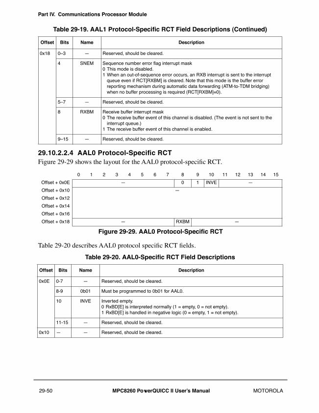
Part IV. Communications Processor Module
29.10.2.2.4 AAL0 Protocol-SpeciÞc RCT Figure 29-29 shows the layout for the AAL0 protocol-speciÞc RCT.
Table 29-20 describes AAL0 protocol speciÞc RCT Þelds.
0x18 0Ð3 Ñ Reserved, should be cleared.
4 SNEM Sequence number error ßag interrupt mask0 This mode is disabled.1 When an out-of-sequence error occurs, an RXB interrupt is sent to the interrupt
queue even if RCT[RXBM] is cleared. Note that this mode is the buffer error reporting mechanism during automatic data forwarding (ATM-to-TDM bridging) when no buffer processing is required (RCT[RXBM]=0).
5Ð7 Ñ Reserved, should be cleared.
8 RXBM Receive buffer interrupt mask0 The receive buffer event of this channel is disabled. (The event is not sent to the
interrupt queue.)1 The receive buffer event of this channel is enabled.
9Ð15 Ñ Reserved, should be cleared.
0 1 2 3 4 5 6 7 8 9 10 11 12 13 14 15
Offset + 0x0E Ñ 0 1 INVE Ñ
Offset + 0x10 Ñ
Offset + 0x12
Offset + 0x14
Offset + 0x16
Offset + 0x18 Ñ RXBM Ñ
Figure 29-29. AAL0 Protocol-Specific RCT
Table 29-20. AAL0-Specific RCT Field Descriptions
Offset Bits Name Description
0x0E 0-7 Ñ Reserved, should be cleared.
8-9 0b01 Must be programmed to 0b01 for AAL0.
10 INVE Inverted empty. 0 RxBD[E] is interpreted normally (1 = empty, 0 = not empty).1 RxBD[E] is handled in negative logic (0 = empty, 1 = not empty).
11-15 Ñ Reserved, should be cleared.
0x10 Ñ Ñ Reserved, should be cleared.
Table 29-19. AAL1 Protocol-Specific RCT Field Descriptions (Continued)
Offset Bits Name Description
29-50 MPC8260 PowerQUICC II UserÕs Manual MOTOROLA
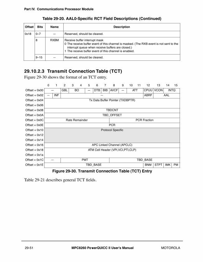
Part IV. Communications Processor Module
29.10.2.3 Transmit Connection Table (TCT)Figure 29-30 shows the format of an TCT entry.
Table 29-21 describes general TCT Þelds.
0x18 0Ð7 Ñ Reserved, should be cleared.
8 RXBM Receive buffer interrupt mask0 The receive buffer event of this channel is masked. (The RXB event is not sent to the
interrupt queue when receive buffers are closed.)1 The receive buffer event of this channel is enabled.
9Ð15 Ñ Reserved, should be cleared.
0 1 2 3 4 5 6 7 8 9 10 11 12 13 14 15
Offset + 0x00 Ñ GBL BO Ñ DTB BIB AVCF Ñ ATT CPUU VCON INTQ
Offset + 0x02 Ñ INF Ñ ABRF AAL
Offset + 0x04 Tx Data Buffer Pointer (TXDBPTR)
Offset + 0x06
Offset + 0x08 TBDCNT
Offset + 0x0A TBD_OFFSET
Offset + 0x0C Rate Remainder PCR Fraction
Offset + 0x0E PCR
Offset + 0x10 Protocol SpeciÞc
Offset + 0x12
Offset + 0x14
Offset + 0x16 APC Linked Channel (APCLC)
Offset + 0x18 ATM Cell Header (VPI,VCI,PTI,CLP)
Offset + 0x1a
Offset + 0x1C Ñ PMT TBD_BASE
Offset + 0x1E TBD_BASE BNM STPT IMK PM
Figure 29-30. Transmit Connection Table (TCT) Entry
Table 29-20. AAL0-Specific RCT Field Descriptions (Continued)
Offset Bits Name Description
29-51 MPC8260 PowerQUICC II UserÕs Manual MOTOROLA
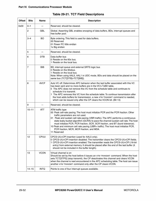
Part IV. Communications Processor Module
Table 29-21. TCT Field Descriptions
Offset Bits Name Description
0x00 0Ð1 Ñ Reserved, should be cleared.
2 GBL Global. Asserting GBL enables snooping of data buffers, BDs, interrupt queues and free buffer pool.
3Ð4 BO Byte ordering. This Þeld is used for data buffers.00 Reserved01 Power PC little endian1x Big endian
5 Ñ Reserved, should be cleared.
6 DTB Data buffer bus0 Reside on the 60x bus.1 Reside on the local bus.
7 BIB BD, interrupt queue and external SRTS logic bus0 Reside on the 60xbus.1 Reside on the local bus.Note: When using AAL5, AAL1 in UDC mode, BDs and data should be placed on the same bus (TCT[DTB]=TCT[BIB]).
8 AVCF Auto VC off. Determines APC behavior when the last buffer associated with this VC has been sent and no more buffers are in the VCÕs TxBD table, 0 The APC does not remove this VC from the schedule table and continues to
schedule it to transmit.1 The APC removes this VC from the schedule table. To continue transmission after
the host adds buffers for transmission, a new ATM TRANSMIT command is needed, which can be issued only after the CP clears the VCON bit. (Bit 13)
9 Ñ Reserved, should be cleared.
10Ð11 ATT ATM trafÞc type00 Peak cell-rate pacing. The host must initialize PCR and the PCR fraction. Other
trafÞc parameters are not used.01 Peak and sustain cell rate pacing (VBR trafÞc). The APC performs a continuous-
state leaky bucket algorithm (GCRA) to pace the channel-sustain cell rate. The host must initialize PCR, PCR fraction, SCR, SCR fraction, and BT (burst tolerance).
10 Peak and minimum cell rate pacing (UBR+ trafÞc). The host must initialize PCR, PCR fraction, MCR, MCR fraction, and MDA.
11 Reserved
12 CPUU CPCS-UU+CPI insertion (used for AAL5 only).0 CPCS-UU+CPI insertion disabled. The transmitter clears the CPCS-UU+CPI Þelds.1 CPCS-UU+CPI insertion enabled. The transmitter reads the CPCS-UU+CPI (16-bit
entry) from external memory. It should be placed after the end of the last buffer (it should not be included in the buffer length).
13 VCON Virtual channel is onShould be set by the host before it issues an ATM TRANSMIT command. When the host sets TCT[STPS] (stop transmit), the CP deactivates this channel and clears VCON when the channel is next encountered in the APC scheduling table. The host can issue another ATM TRANSMIT command only after the CP clears VCON.
14Ð15 INTQ Points to one of four interrupt queues available.
29-52 MPC8260 PowerQUICC II UserÕs Manual MOTOROLA
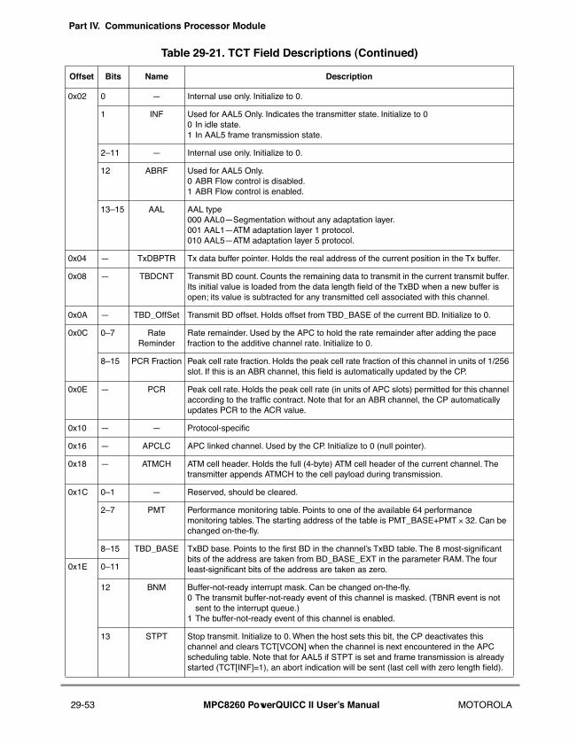
Part IV. Communications Processor Module
0x02 0 Ñ Internal use only. Initialize to 0.
1 INF Used for AAL5 Only. Indicates the transmitter state. Initialize to 00 In idle state.1 In AAL5 frame transmission state.
2Ð11 Ñ Internal use only. Initialize to 0.
12 ABRF Used for AAL5 Only.0 ABR Flow control is disabled.1 ABR Flow control is enabled.
13Ð15 AAL AAL type000 AAL0ÑSegmentation without any adaptation layer.001 AAL1ÑATM adaptation layer 1 protocol. 010 AAL5ÑATM adaptation layer 5 protocol.
0x04 Ñ TxDBPTR Tx data buffer pointer. Holds the real address of the current position in the Tx buffer.
0x08 Ñ TBDCNT Transmit BD count. Counts the remaining data to transmit in the current transmit buffer. Its initial value is loaded from the data length Þeld of the TxBD when a new buffer is open; its value is subtracted for any transmitted cell associated with this channel.
0x0A Ñ TBD_OffSet Transmit BD offset. Holds offset from TBD_BASE of the current BD. Initialize to 0.
0x0C 0Ð7 Rate Reminder
Rate remainder. Used by the APC to hold the rate remainder after adding the pace fraction to the additive channel rate. Initialize to 0.
8Ð15 PCR Fraction Peak cell rate fraction. Holds the peak cell rate fraction of this channel in units of 1/256 slot. If this is an ABR channel, this Þeld is automatically updated by the CP.
0x0E Ñ PCR Peak cell rate. Holds the peak cell rate (in units of APC slots) permitted for this channel according to the trafÞc contract. Note that for an ABR channel, the CP automatically updates PCR to the ACR value.
0x10 Ñ Ñ Protocol-speciÞc
0x16 Ñ APCLC APC linked channel. Used by the CP. Initialize to 0 (null pointer).
0x18 Ñ ATMCH ATM cell header. Holds the full (4-byte) ATM cell header of the current channel. The transmitter appends ATMCH to the cell payload during transmission.
0x1C 0Ð1 Ñ Reserved, should be cleared.
2Ð7 PMT Performance monitoring table. Points to one of the available 64 performance monitoring tables. The starting address of the table is PMT_BASE+PMT ´ 32. Can be changed on-the-ßy.
8Ð15 TBD_BASE TxBD base. Points to the Þrst BD in the channelÕs TxBD table. The 8 most-signiÞcant bits of the address are taken from BD_BASE_EXT in the parameter RAM. The four least-signiÞcant bits of the address are taken as zero. 0x1E 0Ð11
12 BNM Buffer-not-ready interrupt mask. Can be changed on-the-ßy.0 The transmit buffer-not-ready event of this channel is masked. (TBNR event is not
sent to the interrupt queue.)1 The buffer-not-ready event of this channel is enabled.
13 STPT Stop transmit. Initialize to 0. When the host sets this bit, the CP deactivates this channel and clears TCT[VCON] when the channel is next encountered in the APC scheduling table. Note that for AAL5 if STPT is set and frame transmission is already started (TCT[INF]=1), an abort indication will be sent (last cell with zero length Þeld).
Table 29-21. TCT Field Descriptions (Continued)
Offset Bits Name Description
29-53 MPC8260 PowerQUICC II UserÕs Manual MOTOROLA
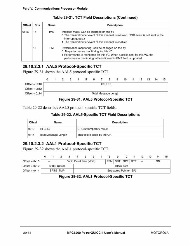
Part IV. Communications Processor Module
29.10.2.3.1 AAL5 Protocol-SpeciÞc TCTFigure 29-31 shows the AAL5 protocol-speciÞc TCT.
Table 29-22 describes AAL5 protocol-speciÞc TCT Þelds.
29.10.2.3.2 AAL1 Protocol-SpeciÞc TCTFigure 29-32 shows the AAL1 protocol-speciÞc TCT.
0x1E 14 IMK Interrupt mask. Can be changed on-the-ßy.0 The transmit buffer event of this channel is masked. (TXB event is not sent to the
interrupt queue.)1 The transmit buffer event of this channel is enabled.
15 PM Performance monitoring. Can be changed on-the-ßy.0 No performance monitoring for this VC.1 Performance is monitored for this VC. When a cell is sent for this VC, the
performance monitoring table indicated in PMT Þeld is updated.
0 1 2 3 4 5 6 7 8 9 10 11 12 13 14 15
Offset + 0x10 Tx CRC
Offset + 0x12
Offset + 0x14 Total Message Length
Figure 29-31. AAL5 Protocol-Specific TCT
Table 29-22. AAL5-Specific TCT Field Descriptions
Offset Name Description
0x10 Tx CRC CRC32 temporary result.
0x14 Total Message Length This Þeld is used by the CP.
0 1 2 3 4 5 6 7 8 9 10 11 12 13 14 15
Offset + 0x10 Ñ Valid Octet Size (VOS) PFM SRT SPF STF Ñ SN
Offset + 0x12 SRTS Device Block Size
Offset + 0x14 SRTS_TMP Structured Pointer (SP)
Figure 29-32. AAL1 Protocol-Specific TCT
Table 29-21. TCT Field Descriptions (Continued)
Offset Bits Name Description
29-54 MPC8260 PowerQUICC II UserÕs Manual MOTOROLA
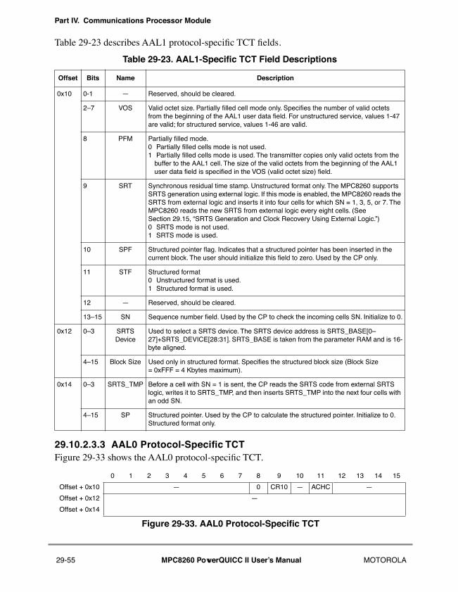
Part IV. Communications Processor Module
Table 29-23 describes AAL1 protocol-speciÞc TCT Þelds.
29.10.2.3.3 AAL0 Protocol-SpeciÞc TCTFigure 29-33 shows the AAL0 protocol-speciÞc TCT.
Table 29-23. AAL1-Specific TCT Field Descriptions
Offset Bits Name Description
0x10 0-1 Ñ Reserved, should be cleared.
2Ð7 VOS Valid octet size. Partially Þlled cell mode only. SpeciÞes the number of valid octets from the beginning of the AAL1 user data Þeld. For unstructured service, values 1-47 are valid; for structured service, values 1-46 are valid.
8 PFM Partially Þlled mode. 0 Partially Þlled cells mode is not used.1 Partially Þlled cells mode is used. The transmitter copies only valid octets from the
buffer to the AAL1 cell. The size of the valid octets from the beginning of the AAL1 user data Þeld is speciÞed in the VOS (valid octet size) Þeld.
9 SRT Synchronous residual time stamp. Unstructured format only. The MPC8260 supports SRTS generation using external logic. If this mode is enabled, the MPC8260 reads the SRTS from external logic and inserts it into four cells for which SN = 1, 3, 5, or 7. The MPC8260 reads the new SRTS from external logic every eight cells. (See Section 29.15, ÒSRTS Generation and Clock Recovery Using External Logic.Ó)0 SRTS mode is not used.1 SRTS mode is used.
10 SPF Structured pointer ßag. Indicates that a structured pointer has been inserted in the current block. The user should initialize this Þeld to zero. Used by the CP only.
11 STF Structured format0 Unstructured format is used.1 Structured format is used.
12 Ñ Reserved, should be cleared.
13Ð15 SN Sequence number Þeld. Used by the CP to check the incoming cells SN. Initialize to 0.
0x12 0Ð3 SRTS Device
Used to select a SRTS device. The SRTS device address is SRTS_BASE[0Ð27]+SRTS_DEVICE[28:31]. SRTS_BASE is taken from the parameter RAM and is 16-byte aligned.
4Ð15 Block Size Used only in structured format. SpeciÞes the structured block size (Block Size= 0xFFF = 4 Kbytes maximum).
0x14 0Ð3 SRTS_TMP Before a cell with SN = 1 is sent, the CP reads the SRTS code from external SRTS logic, writes it to SRTS_TMP, and then inserts SRTS_TMP into the next four cells with an odd SN.
4Ð15 SP Structured pointer. Used by the CP to calculate the structured pointer. Initialize to 0. Structured format only.
0 1 2 3 4 5 6 7 8 9 10 11 12 13 14 15
Offset + 0x10 Ñ 0 CR10 Ñ ACHC Ñ
Offset + 0x12 Ñ
Offset + 0x14
Figure 29-33. AAL0 Protocol-Specific TCT
29-55 MPC8260 PowerQUICC II UserÕs Manual MOTOROLA
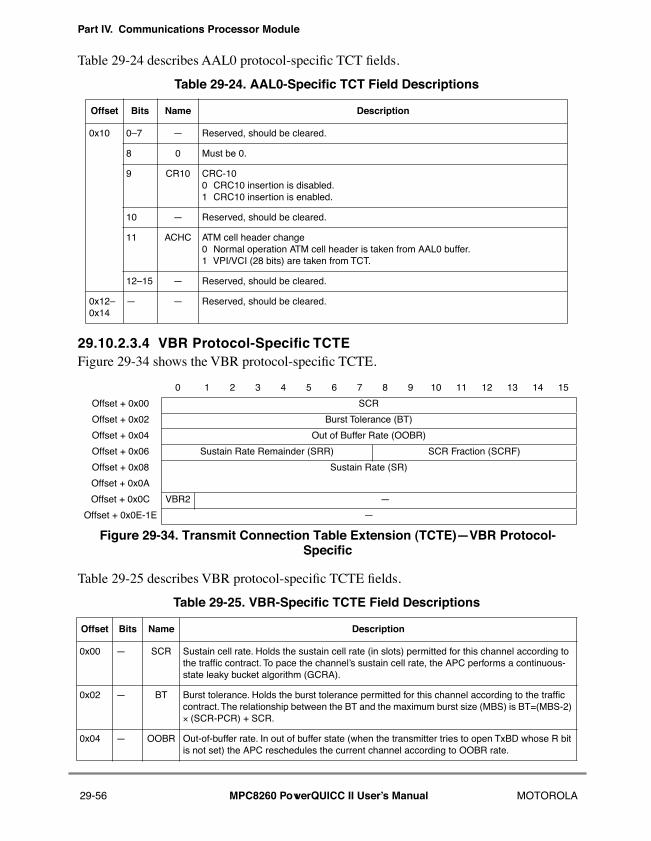
Part IV. Communications Processor Module
Table 29-24 describes AAL0 protocol-speciÞc TCT Þelds.
29.10.2.3.4 VBR Protocol-SpeciÞc TCTEFigure 29-34 shows the VBR protocol-speciÞc TCTE.
Table 29-25 describes VBR protocol-speciÞc TCTE Þelds.
Table 29-24. AAL0-Specific TCT Field Descriptions
Offset Bits Name Description
0x10 0Ð7 Ñ Reserved, should be cleared.
8 0 Must be 0.
9 CR10 CRC-100 CRC10 insertion is disabled.1 CRC10 insertion is enabled.
10 Ñ Reserved, should be cleared.
11 ACHC ATM cell header change0 Normal operation ATM cell header is taken from AAL0 buffer.1 VPI/VCI (28 bits) are taken from TCT.
12Ð15 Ñ Reserved, should be cleared.
0x12Ð0x14
Ñ Ñ Reserved, should be cleared.
0 1 2 3 4 5 6 7 8 9 10 11 12 13 14 15
Offset + 0x00 SCR
Offset + 0x02 Burst Tolerance (BT)
Offset + 0x04 Out of Buffer Rate (OOBR)
Offset + 0x06 Sustain Rate Remainder (SRR) SCR Fraction (SCRF)
Offset + 0x08 Sustain Rate (SR)
Offset + 0x0A
Offset + 0x0C VBR2 Ñ
Offset + 0x0E-1E Ñ
Figure 29-34. Transmit Connection Table Extension (TCTE)ÑVBR Protocol-Specific
Table 29-25. VBR-Specific TCTE Field Descriptions
Offset Bits Name Description
0x00 Ñ SCR Sustain cell rate. Holds the sustain cell rate (in slots) permitted for this channel according to the trafÞc contract. To pace the channelÕs sustain cell rate, the APC performs a continuous-state leaky bucket algorithm (GCRA).
0x02 Ñ BT Burst tolerance. Holds the burst tolerance permitted for this channel according to the trafÞc contract. The relationship between the BT and the maximum burst size (MBS) is BT=(MBS-2) ´ (SCR-PCR) + SCR.
0x04 Ñ OOBR Out-of-buffer rate. In out of buffer state (when the transmitter tries to open TxBD whose R bit is not set) the APC reschedules the current channel according to OOBR rate.
29-56 MPC8260 PowerQUICC II UserÕs Manual MOTOROLA
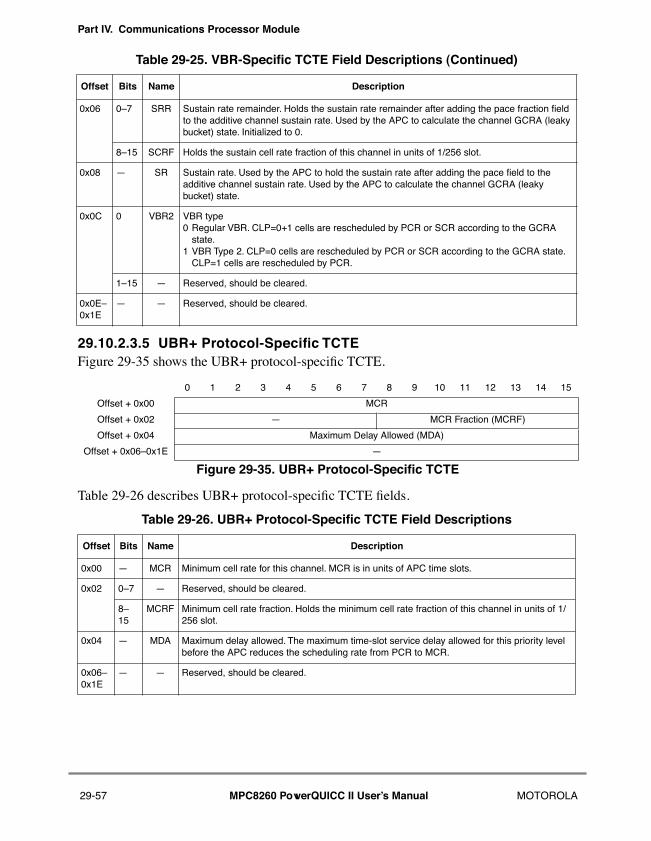
Part IV. Communications Processor Module
29.10.2.3.5 UBR+ Protocol-SpeciÞc TCTEFigure 29-35 shows the UBR+ protocol-speciÞc TCTE.
Table 29-26 describes UBR+ protocol-speciÞc TCTE Þelds.
0x06 0Ð7 SRR Sustain rate remainder. Holds the sustain rate remainder after adding the pace fraction Þeld to the additive channel sustain rate. Used by the APC to calculate the channel GCRA (leaky bucket) state. Initialized to 0.
8Ð15 SCRF Holds the sustain cell rate fraction of this channel in units of 1/256 slot.
0x08 Ñ SR Sustain rate. Used by the APC to hold the sustain rate after adding the pace Þeld to the additive channel sustain rate. Used by the APC to calculate the channel GCRA (leaky bucket) state.
0x0C 0 VBR2 VBR type0 Regular VBR. CLP=0+1 cells are rescheduled by PCR or SCR according to the GCRA
state.1 VBR Type 2. CLP=0 cells are rescheduled by PCR or SCR according to the GCRA state.
CLP=1 cells are rescheduled by PCR.
1Ð15 Ñ Reserved, should be cleared.
0x0EÐ0x1E
Ñ Ñ Reserved, should be cleared.
0 1 2 3 4 5 6 7 8 9 10 11 12 13 14 15
Offset + 0x00 MCR
Offset + 0x02 Ñ MCR Fraction (MCRF)
Offset + 0x04 Maximum Delay Allowed (MDA)
Offset + 0x06Ð0x1E Ñ
Figure 29-35. UBR+ Protocol-Specific TCTE
Table 29-26. UBR+ Protocol-Specific TCTE Field Descriptions
Offset Bits Name Description
0x00 Ñ MCR Minimum cell rate for this channel. MCR is in units of APC time slots.
0x02 0Ð7 Ñ Reserved, should be cleared.
8Ð15
MCRF Minimum cell rate fraction. Holds the minimum cell rate fraction of this channel in units of 1/256 slot.
0x04 Ñ MDA Maximum delay allowed. The maximum time-slot service delay allowed for this priority level before the APC reduces the scheduling rate from PCR to MCR.
0x06Ð0x1E
Ñ Ñ Reserved, should be cleared.
Table 29-25. VBR-Specific TCTE Field Descriptions (Continued)
Offset Bits Name Description
29-57 MPC8260 PowerQUICC II UserÕs Manual MOTOROLA
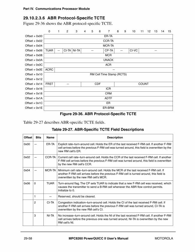
Part IV. Communications Processor Module
29.10.2.3.6 ABR Protocol-SpeciÞc TCTEFigure 29-36 shows the ABR protocol-speciÞc TCTE.
Table 29-27 describes ABR-speciÞc TCTE Þelds.
0 1 2 3 4 5 6 7 8 9 10 11 12 13 14 15
Offset + 0x00 ER-TA
Offset + 0x02 CCR-TA
Offset + 0x04 MCR-TA
Offset + 0x06 TUAR Ñ CI-TA NI-TA Ñ CP-TA Ñ CI-VC Ñ
Offset + 0x08 MCR
Offset + 0x0A UNACK
Offset + 0x0C ACR
Offset + 0x0E ACRC Ñ
Offset + 0x10 RM Cell Time Stamp (RCTS)
Offset + 0x12
Offset + 0x14 FRST Ñ CDF COUNT
Offset + 0x16 ICR
Offset + 0x18 CRM
Offset + 0x1A ADTF
Offset + 0x1C ER
Offset + 0x1E ER-BRM
Figure 29-36. ABR Protocol-Specific TCTE
Table 29-27. ABR-Specific TCTE Field Descriptions
Offset Bits Name Description
0x00 Ñ ER-TA Explicit rateÐturn-around cell. Holds the ER of the last received F-RM cell. If another F-RM cell arrives before the previous F-RM cell was turned around, this Þeld is overwritten by the new RM cellÕs ER.
0x02 Ñ CCR-TA Current cell rateÐturn-around cell. Holds the CCR of the last received F-RM cell. If another F-RM cell arrives before the previous F-RM cell was turned around, this Þeld is overwritten by the new RM cellÕs CCR.
0x04 Ñ MCR-TA Minimum cell rateÐturn-around cell. Holds the MCR of the last received F-RM cell. If another F-RM cell arrives before the previous F-RM cell is turned around, this Þeld is overwritten by the new RM cellÕs MCR.
0x06 0 TUAR Turn-around ßag. The CP sets TUAR to indicate that a new F-RM cell was received, which causes the transmitter to send a B-RM cell whenever the ABR ßow control permits. Initialize to 0.
1 Ñ Reserved, should be cleared.
2 CI-TA Congestion indicationÐturn-around cell. Holds the CI of the last received F-RM cell. If another F-RM cell arrives before the previous F-RM cell was turned around, CI-TA is overwritten by the new RM cellÕs CI.
3 NI-TA No increaseÐturn-around cell. Holds the NI of the last received F-RM cell. If another F-RM cell arrives before the previous one was turned around, NI-TA is overwritten by the new RM cellÕs NI.
29-58 MPC8260 PowerQUICC II UserÕs Manual MOTOROLA
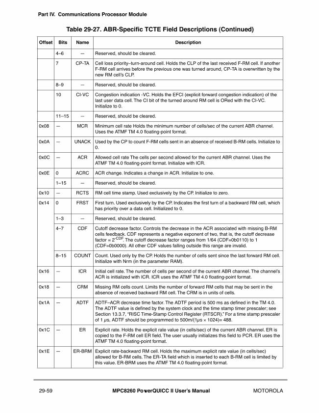
Part IV. Communications Processor Module
4Ð6 Ñ Reserved, should be cleared.
7 CP-TA Cell loss priorityÐturn-around cell. Holds the CLP of the last received F-RM cell. If another F-RM cell arrives before the previous one was turned around, CP-TA is overwritten by the new RM cellÕs CLP.
8Ð9 Ñ Reserved, should be cleared.
10 CI-VC Congestion indication -VC. Holds the EFCI (explicit forward congestion indication) of the last user data cell. The CI bit of the turned around RM cell is ORed with the CI-VC. Initialize to 0.
11Ð15 Ñ Reserved, should be cleared.
0x08 Ñ MCR Minimum cell rate Holds the minimum number of cells/sec of the current ABR channel. Uses the ATMF TM 4.0 ßoating-point format.
0x0A Ñ UNACK Used by the CP to count F-RM cells sent in an absence of received B-RM cells. Initialize to 0.
0x0C Ñ ACR Allowed cell rate The cells per second allowed for the current ABR channel. Uses the ATMF TM 4.0 ßoating-point format. Initialize with ICR.
0x0E 0 ACRC ACR change. Indicates a change in ACR. Initialize to one.
1Ð15 Ñ Reserved, should be cleared.
0x10 Ñ RCTS RM cell time stamp. Used exclusively by the CP. Initialize to zero.
0x14 0 FRST First turn. Used exclusively by the CP. Indicates the Þrst turn of a backward RM cell, which has priority over a data cell. Initialized to 0.
1Ð3 Ñ Reserved, should be cleared.
4Ð7 CDF Cutoff decrease factor. Controls the decrease in the ACR associated with missing B-RM cells feedback. CDF represents a negative exponent of two, that is, the cutoff decrease factor = 2-CDF. The cutoff decrease factor ranges from 1/64 (CDF=0b0110) to 1 (CDF=0b0000). All other CDF values falling outside this range are invalid.
8Ð15 COUNT Count. Used only by the CP. Holds the number of cells sent since the last forward RM cell. Initialize with Nrm (in the parameter RAM).
0x16 Ñ ICR Initial cell rate. The number of cells per second of the current ABR channel. The channelÕs ACR is initialized with ICR. ICR uses the ATMF TM 4.0 ßoating-point format.
0x18 Ñ CRM Missing RM cells count. Limits the number of forward RM cells that may be sent in the absence of received backward RM cell. The CRM is in units of cells.
0x1A Ñ ADTF ADTFÐACR decrease time factor. The ADTF period is 500 ms as deÞned in the TM 4.0. The ADTF value is deÞned by the system clock and the time stamp timer prescaler; see Section 13.3.7, ÒRISC Time-Stamp Control Register (RTSCR).Ó For a time stamp prescaler of 1 µs, ADTF should be programmed to 500m/(1µs ´ 1024)= 488.
0x1C Ñ ER Explicit rate. Holds the explicit rate value (in cells/sec) of the current ABR channel. ER is copied to the F-RM cell ER Þeld. The user usually initializes this Þeld to PCR. ER uses the ATMF TM 4.0 ßoating-point format.
0x1E Ñ ER-BRM Explicit rate-backward RM cell. Holds the maximum explicit rate value (in cells/sec) allowed for B-RM cells. The ER-TA Þeld which is inserted to each B-RM cell is limited by this value. ER-BRM uses the ATMF TM 4.0 ßoating-point format.
Table 29-27. ABR-Specific TCTE Field Descriptions (Continued)
Offset Bits Name Description
29-59 MPC8260 PowerQUICC II UserÕs Manual MOTOROLA
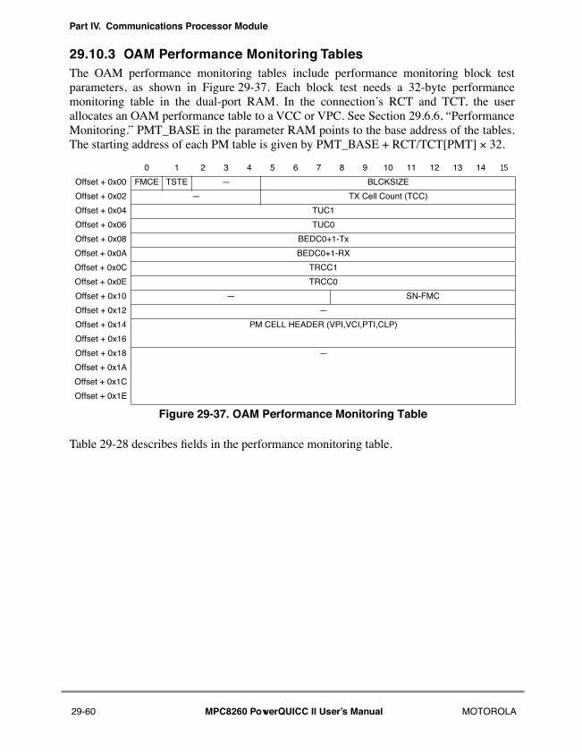
Part IV. Communications Processor Module
29.10.3 OAM Performance Monitoring TablesThe OAM performance monitoring tables include performance monitoring block testparameters, as shown in Figure 29-37. Each block test needs a 32-byte performancemonitoring table in the dual-port RAM. In the connectionÕs RCT and TCT, the userallocates an OAM performance table to a VCC or VPC. See Section 29.6.6, ÒPerformanceMonitoring.Ó PMT_BASE in the parameter RAM points to the base address of the tables.The starting address of each PM table is given by PMT_BASE + RCT/TCT[PMT] ´ 32.
Table 29-28 describes Þelds in the performance monitoring table.
0 1 2 3 4 5 6 7 8 9 10 11 12 13 14 15
Offset + 0x00 FMCE TSTE Ñ BLCKSIZE
Offset + 0x02 Ñ TX Cell Count (TCC)
Offset + 0x04 TUC1
Offset + 0x06 TUC0
Offset + 0x08 BEDC0+1-Tx
Offset + 0x0A BEDC0+1-RX
Offset + 0x0C TRCC1
Offset + 0x0E TRCC0
Offset + 0x10 Ñ SN-FMC
Offset + 0x12 Ñ
Offset + 0x14 PM CELL HEADER (VPI,VCI,PTI,CLP)
Offset + 0x16
Offset + 0x18 Ñ
Offset + 0x1A
Offset + 0x1C
Offset + 0x1E
Figure 29-37. OAM Performance Monitoring Table
29-60 MPC8260 PowerQUICC II UserÕs Manual MOTOROLA
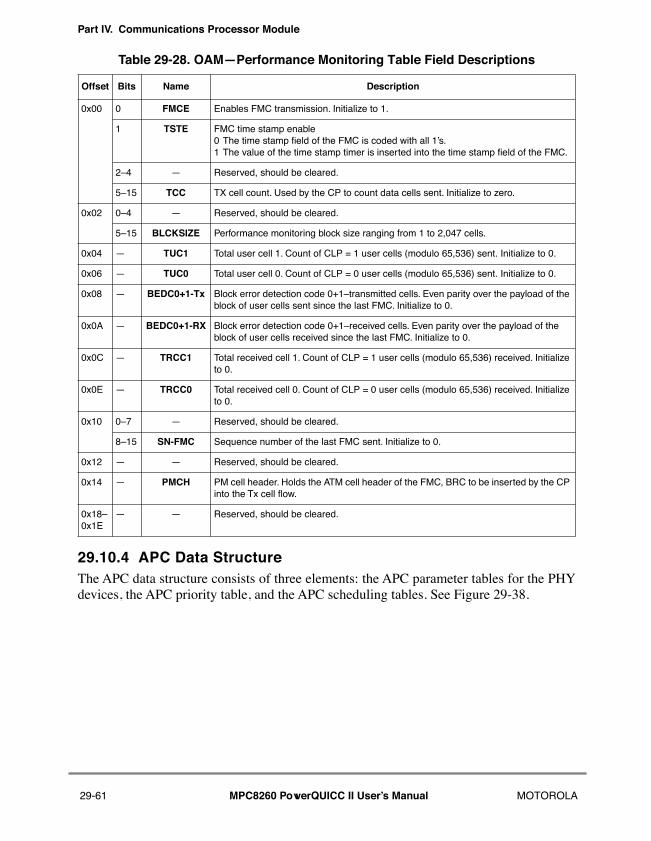
Part IV. Communications Processor Module
29.10.4 APC Data StructureThe APC data structure consists of three elements: the APC parameter tables for the PHYdevices, the APC priority table, and the APC scheduling tables. See Figure 29-38.
Table 29-28. OAMÑPerformance Monitoring Table Field Descriptions
Offset Bits Name Description
0x00 0 FMCE Enables FMC transmission. Initialize to 1.
1 TSTE FMC time stamp enable0 The time stamp Þeld of the FMC is coded with all 1Õs. 1 The value of the time stamp timer is inserted into the time stamp Þeld of the FMC.
2Ð4 Ñ Reserved, should be cleared.
5Ð15 TCC TX cell count. Used by the CP to count data cells sent. Initialize to zero.
0x02 0Ð4 Ñ Reserved, should be cleared.
5Ð15 BLCKSIZE Performance monitoring block size ranging from 1 to 2,047 cells.
0x04 Ñ TUC1 Total user cell 1. Count of CLP = 1 user cells (modulo 65,536) sent. Initialize to 0.
0x06 Ñ TUC0 Total user cell 0. Count of CLP = 0 user cells (modulo 65,536) sent. Initialize to 0.
0x08 Ñ BEDC0+1-Tx Block error detection code 0+1Ðtransmitted cells. Even parity over the payload of the block of user cells sent since the last FMC. Initialize to 0.
0x0A Ñ BEDC0+1-RX Block error detection code 0+1Ðreceived cells. Even parity over the payload of the block of user cells received since the last FMC. Initialize to 0.
0x0C Ñ TRCC1 Total received cell 1. Count of CLP = 1 user cells (modulo 65,536) received. Initialize to 0.
0x0E Ñ TRCC0 Total received cell 0. Count of CLP = 0 user cells (modulo 65,536) received. Initialize to 0.
0x10 0Ð7 Ñ Reserved, should be cleared.
8Ð15 SN-FMC Sequence number of the last FMC sent. Initialize to 0.
0x12 Ñ Ñ Reserved, should be cleared.
0x14 Ñ PMCH PM cell header. Holds the ATM cell header of the FMC, BRC to be inserted by the CP into the Tx cell ßow.
0x18Ð0x1E
Ñ Ñ Reserved, should be cleared.
29-61 MPC8260 PowerQUICC II UserÕs Manual MOTOROLA
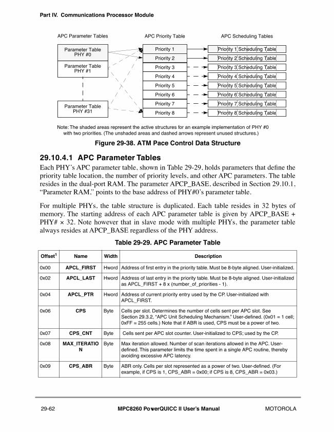
Part IV. Communications Processor Module
Figure 29-38. ATM Pace Control Data Structure
29.10.4.1 APC Parameter TablesEach PHYÕs APC parameter table, shown in Table 29-29, holds parameters that deÞne thepriority table location, the number of priority levels, and other APC parameters. The tableresides in the dual-port RAM. The parameter APCP_BASE, described in Section 29.10.1,ÒParameter RAM,Ó points to the base address of PHY#0Õs parameter table.
For multiple PHYs, the table structure is duplicated. Each table resides in 32 bytes ofmemory. The starting address of each APC parameter table is given by APCP_BASE +PHY# ´ 32. Note however that in slave mode with multiple PHYs, the parameter tablealways resides at APCP_BASE regardless of the PHY address.
Table 29-29. APC Parameter Table
Offset1 Name Width Description
0x00 APCL_FIRST Hword Address of Þrst entry in the priority table. Must be 8-byte aligned. User-initialized.
0x02 APCL_LAST Hword Address of last entry in the priority table. Must be 8-byte aligned. User-initialized as APCL_FIRST + 8 x (number_of_priorities - 1).
0x04 APCL_PTR Hword Address of current priority entry used by the CP. User-initialized with APCL_FIRST.
0x06 CPS Byte Cells per slot. Determines the number of cells sent per APC slot. See Section 29.3.2, ÒAPC Unit Scheduling Mechanism.Ó User-deÞned. (0x01 = 1 cell; 0xFF = 255 cells.) Note that if ABR is used, CPS must be a power of two.
0x07 CPS_CNT Byte Cells sent per APC slot counter. User-initialized to CPS; used by the CP.
0x08 MAX_ITERATION
Byte Max iteration allowed. Number of scan iterations allowed in the APC. User-deÞned. This parameter limits the time spent in a single APC routine, thereby avoiding excessive APC latency.
0x09 CPS_ABR Byte ABR only. Cells per slot represented as a power of two. User-deÞned. (For example, if CPS is 1, CPS_ABR = 0x00; if CPS is 8, CPS_ABR = 0x03.)
Priority 1
APC Priority TableAPC Parameter Tables
Parameter TablePHY #0
Parameter TablePHY #1
Parameter TablePHY #31
Priority 2
Priority 3
Priority 4
Priority 5
Priority 6
Priority 7
Priority 8
APC Scheduling Tables
Priority 1 Scheduling Table
Priority 2 Scheduling Table
Priority 3 Scheduling Table
Priority 4 Scheduling Table
Priority 5 Scheduling Table
Priority 6 Scheduling Table
Priority 7 Scheduling Table
Priority 8 Scheduling Table
Note: The shaded areas represent the active structures for an example implementation of PHY #0 with two priorities. (The unshaded areas and dashed arrows represent unused structures.)
29-62 MPC8260 PowerQUICC II UserÕs Manual MOTOROLA
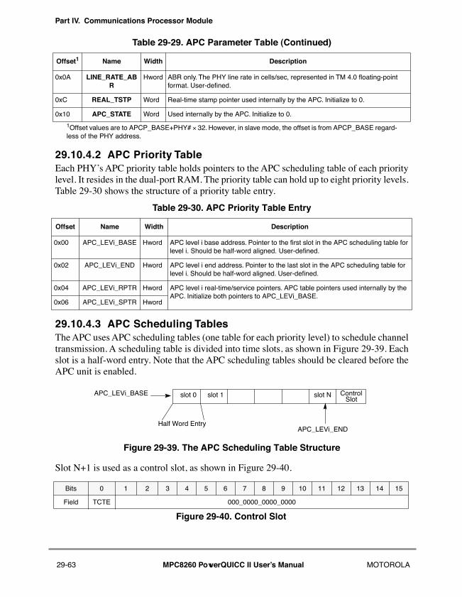
Part IV. Communications Processor Module
29.10.4.2 APC Priority TableEach PHYÕs APC priority table holds pointers to the APC scheduling table of each prioritylevel. It resides in the dual-port RAM. The priority table can hold up to eight priority levels.Table 29-30 shows the structure of a priority table entry.
29.10.4.3 APC Scheduling TablesThe APC uses APC scheduling tables (one table for each priority level) to schedule channeltransmission. A scheduling table is divided into time slots, as shown in Figure 29-39. Eachslot is a half-word entry. Note that the APC scheduling tables should be cleared before theAPC unit is enabled.
Figure 29-39. The APC Scheduling Table Structure
Slot N+1 is used as a control slot, as shown in Figure 29-40.
0x0A LINE_RATE_ABR
Hword ABR only. The PHY line rate in cells/sec, represented in TM 4.0 ßoating-point format. User-deÞned.
0xC REAL_TSTP Word Real-time stamp pointer used internally by the APC. Initialize to 0.
0x10 APC_STATE Word Used internally by the APC. Initialize to 0.
1Offset values are to APCP_BASE+PHY# ́ 32. However, in slave mode, the offset is from APCP_BASE regard-less of the PHY address.
Table 29-30. APC Priority Table Entry
Offset Name Width Description
0x00 APC_LEVi_BASE Hword APC level i base address. Pointer to the first slot in the APC scheduling table for level i. Should be half-word aligned. User-deÞned.
0x02 APC_LEVi_END Hword APC level i end address. Pointer to the last slot in the APC scheduling table for level i. Should be half-word aligned. User-deÞned.
0x04 APC_LEVi_RPTR Hword APC level i real-time/service pointers. APC table pointers used internally by the APC. Initialize both pointers to APC_LEVi_BASE.
0x06 APC_LEVi_SPTR Hword
Bits 0 1 2 3 4 5 6 7 8 9 10 11 12 13 14 15
Field TCTE 000_0000_0000_0000
Figure 29-40. Control Slot
Table 29-29. APC Parameter Table (Continued)
Offset1 Name Width Description
APC_LEVi_BASE
APC_LEVi_ENDHalf Word Entry
slot 0 slot 1 slot N ControlSlot
29-63 MPC8260 PowerQUICC II UserÕs Manual MOTOROLA
Part IV. Communications Processor Module
Table 29-31 describes control slot Þelds.
29.10.5 ATM Controller Buffer Descriptors (BDs)Each ATM channel has separate receive and transmit BD tables. The number of BDs perchannel and the size of the buffers is user-deÞned. The last BD in each table holds a wrapindication. Each BD in the TxBD table points to a buffer to send. At the receive side, theuser can choose one of two modes:
¥ Static buffer allocation. In this mode, the user allocates dedicated buffers to each ATM channel (that is, the user associates each BD with one buffer). Static buffer allocation is useful when the connection rate is known and constant and when data must be reassembled in a particular memory space.
¥ Global buffer allocation. Available for AAL5 only. In this mode, buffer allocation is dynamic. The user allocates receive buffers and places them in global buffer pools. When the CP needs a receive buffer, it Þrst fetches a buffer pointer from one of the global buffer pools and writes the pointer to the current RxBD. Global buffer allocation is optimized for allocating memory among many ATM channels with variable data rates, such as ABR channels.
29.10.5.1 Transmit Buffer OperationsThe user prepares a table of BDs pointing to the buffers to be sent. The address of the ÞrstBD is put in the channelÕs TCT[TBD_BASE]. The transmit process starts when the coreissues an ATM TRANSMIT command. The CP reads the Þrst TxBD in the table and sends itsassociated buffer. When the current buffer is Þnished, the CP increments TBD_Offset,which holds the offset from TBD_BASE to the current BD. It then reads the next BD in thetable. If the BD is ready (TxBD[R] = 1), the CP continues sending. If the current BD is notready, the CP polls the ready bit at the channel rate unless TCT[AVCF] = 1, in which casethe CP removes the channel from the APC and clears TCT[VCON]. The core must issue anew ATM TRANSMIT command to restart transmission.
Figure 29-41 shows the ready bit in the TxBD tables and their associated buffers for twoexample ATM channels.
Table 29-31. Control Slot Field Description
Bits Name Description
0 TCTE Used for external channels only.0 Channels in this scheduling table do not use external TCTE. (No external VBR, ABR, UBR+
channels) 1 Channels in this scheduling table use external TCTE. (External VBR, ABR, UBR+ channels)
1Ð15 Ñ Reserved, should be cleared.
29-64 MPC8260 PowerQUICC II UserÕs Manual MOTOROLA
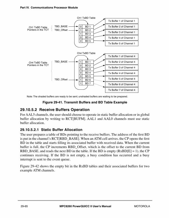
Part IV. Communications Processor Module
Figure 29-41. Transmit Buffers and BD Table Example
29.10.5.2 Receive Buffers OperationFor AAL5 channels, the user should choose to operate in static buffer allocation or in globalbuffer allocation by writing to RCT[BUFM]. AAL1 and AAL0 channels must use staticbuffer allocation.
29.10.5.2.1 Static Buffer AllocationThe user prepares a table of BDs pointing to the receive buffers. The address of the Þrst BDis put in the channelÕs RCT[RBD_BASE]. When an ATM cell arrives, the CP opens the ÞrstBD in the table and starts Þlling its associated buffer with received data. When the currentbuffer is full, the CP increments RBD_Offset, which is the offset to the current BD fromRBD_BASE, and reads the next BD in the table. If the BD is empty (RxBD[E] = 1), the CPcontinues receiving. If the BD is not empty, a busy condition has occurred and a busyinterrupt is sent to the event queue.
Figure 29-42 shows the empty bit in the RxBD tables and their associated buffers for twoexample ATM channels.
Tx Buffer 1 of Channel 1
Tx Buffer 2 of Channel 1
Tx Buffer 3 of Channel 1
Tx Buffer 4 of Channel 1
Tx Buffer 5 of Channel 1
Ch1 TxBD Table
0 BD 11 BD 21 BD 30 BD 40 BD 5
TBD_BASETBD_Offset
Note: The shaded buffers are ready to be sent; unshaded buffers are waiting to be prepared.
Ch1 TxBD TablePointers in the TCT
Tx Buffer 1 of Channel 4
Tx Buffer 2 of Channel 4
Tx Buffer 3 of Channel 4
Tx Buffer 4 of Channel 4
Tx Buffer 5 of Channel 4
Ch4 TxBD Table
1 BD 10 BD 20 BD 30 BD 40 BD 5
TBD_BASE
TBD_Offset
Ch4 TxBD TablePointers in the TCT
1 BD 6BD 7 Tx Buffer 6 of Channel 4
Tx Buffer 7 of Channel 4
1
29-65 MPC8260 PowerQUICC II UserÕs Manual MOTOROLA
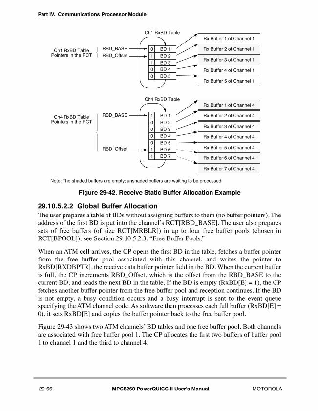
Part IV. Communications Processor Module
Figure 29-42. Receive Static Buffer Allocation Example
29.10.5.2.2 Global Buffer AllocationThe user prepares a table of BDs without assigning buffers to them (no buffer pointers). Theaddress of the Þrst BD is put into the channelÕs RCT[RBD_BASE]. The user also preparessets of free buffers (of size RCT[MRBLR]) in up to four free buffer pools (chosen inRCT[BPOOL]); see Section 29.10.5.2.3, ÒFree Buffer Pools.Ó
When an ATM cell arrives, the CP opens the Þrst BD in the table, fetches a buffer pointerfrom the free buffer pool associated with this channel, and writes the pointer toRxBD[RXDBPTR], the receive data buffer pointer Þeld in the BD. When the current bufferis full, the CP increments RBD_Offset, which is the offset from the RBD_BASE to thecurrent BD, and reads the next BD in the table. If the BD is empty (RxBD[E] = 1), the CPfetches another buffer pointer from the free buffer pool and reception continues. If the BDis not empty, a busy condition occurs and a busy interrupt is sent to the event queuespecifying the ATM channel code. As software then processes each full buffer (RxBD[E] =0), it sets RxBD[E] and copies the buffer pointer back to the free buffer pool.
Figure 29-43 shows two ATM channelsÕ BD tables and one free buffer pool. Both channelsare associated with free buffer pool 1. The CP allocates the Þrst two buffers of buffer pool1 to channel 1 and the third to channel 4.
Rx Buffer 1 of Channel 1
Rx Buffer 2 of Channel 1
Rx Buffer 3 of Channel 1
Rx Buffer 4 of Channel 1
Rx Buffer 5 of Channel 1
Ch1 RxBD Table
0 BD 11 BD 21 BD 30 BD 40 BD 5
RBD_BASERBD_Offset
Note: The shaded buffers are empty; unshaded buffers are waiting to be processed.
Ch1 RxBD TablePointers in the RCT
Rx Buffer 1 of Channel 4
Rx Buffer 2 of Channel 4
Rx Buffer 3 of Channel 4
Rx Buffer 4 of Channel 4
Rx Buffer 5 of Channel 4
Ch4 RxBD Table
1 BD 10 BD 20 BD 30 BD 40 BD 5
RBD_BASE
RBD_Offset
Ch4 RxBD TablePointers in the RCT
1 BD 6BD 7 Rx Buffer 6 of Channel 4
Rx Buffer 7 of Channel 4
1
29-66 MPC8260 PowerQUICC II UserÕs Manual MOTOROLA
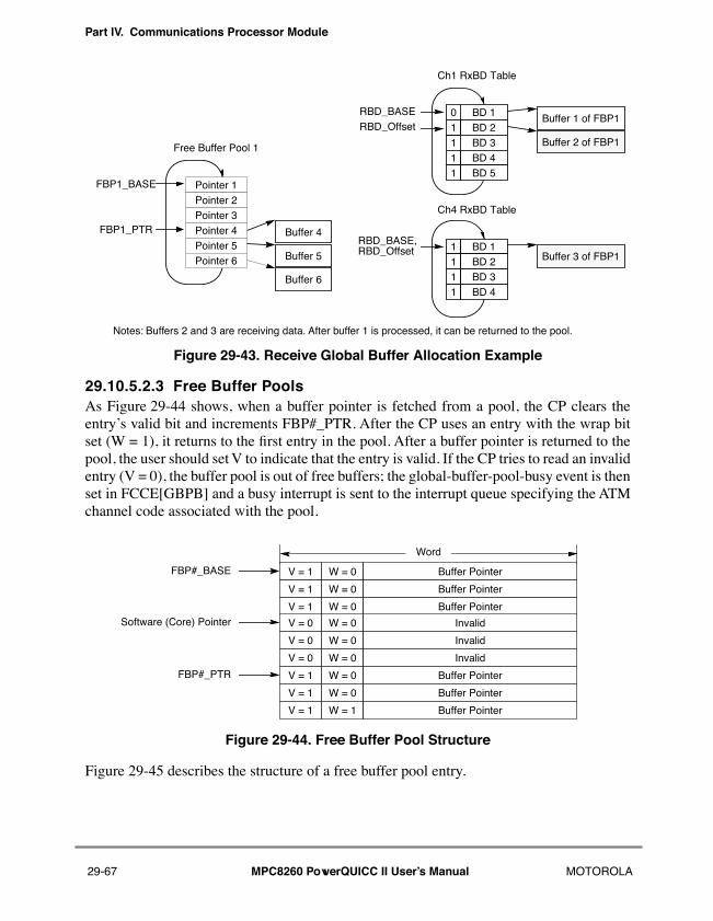
Part IV. Communications Processor Module
Figure 29-43. Receive Global Buffer Allocation Example
29.10.5.2.3 Free Buffer PoolsAs Figure 29-44 shows, when a buffer pointer is fetched from a pool, the CP clears theentryÕs valid bit and increments FBP#_PTR. After the CP uses an entry with the wrap bitset (W = 1), it returns to the Þrst entry in the pool. After a buffer pointer is returned to thepool, the user should set V to indicate that the entry is valid. If the CP tries to read an invalidentry (V = 0), the buffer pool is out of free buffers; the global-buffer-pool-busy event is thenset in FCCE[GBPB] and a busy interrupt is sent to the interrupt queue specifying the ATMchannel code associated with the pool.
Figure 29-44. Free Buffer Pool Structure
Figure 29-45 describes the structure of a free buffer pool entry.
Buffer 1 of FBP1
Buffer 2 of FBP1
Ch1 RxBD Table
0 BD 11 BD 21 BD 31 BD 41 BD 5
RBD_BASERBD_Offset
Buffer 3 of FBP1
Ch4 RxBD Table
1 BD 11 BD 21 BD 31 BD 4
RBD_BASE,RBD_Offset
Free Buffer Pool 1
FBP1_PTR
FBP1_BASE Pointer 1Pointer 2Pointer 3Pointer 4Pointer 5Pointer 6
Buffer 4
Buffer 5
Buffer 6
Notes: Buffers 2 and 3 are receiving data. After buffer 1 is processed, it can be returned to the pool.
V = 1 W = 0 Buffer Pointer
V = 1 W = 0 Buffer Pointer
V = 1 W = 0 Buffer Pointer
V = 0 W = 0 Invalid
V = 0 W = 0 Invalid
V = 0 W = 0 Invalid
V = 1 W = 0 Buffer Pointer
V = 1 W = 0 Buffer Pointer
V = 1 W = 1 Buffer Pointer
FBP#_BASE
Software (Core) Pointer
FBP#_PTR
Word
29-67 MPC8260 PowerQUICC II UserÕs Manual MOTOROLA
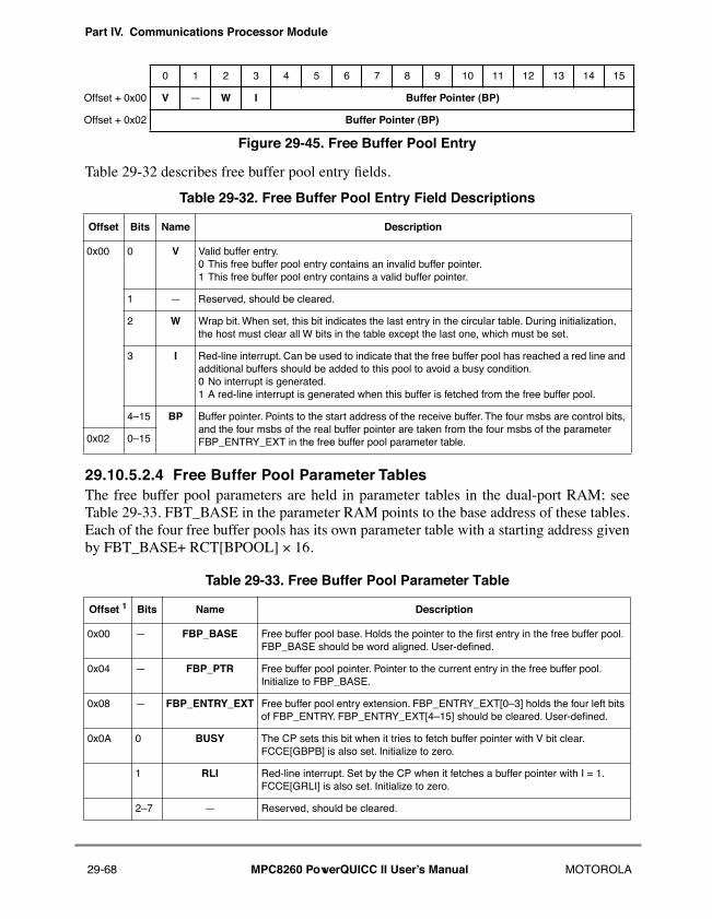
Part IV. Communications Processor Module
Table 29-32 describes free buffer pool entry Þelds.
29.10.5.2.4 Free Buffer Pool Parameter TablesThe free buffer pool parameters are held in parameter tables in the dual-port RAM; seeTable 29-33. FBT_BASE in the parameter RAM points to the base address of these tables.Each of the four free buffer pools has its own parameter table with a starting address givenby FBT_BASE+ RCT[BPOOL] ´ 16.
0 1 2 3 4 5 6 7 8 9 10 11 12 13 14 15
Offset + 0x00 V Ñ W I Buffer Pointer (BP)
Offset + 0x02 Buffer Pointer (BP)
Figure 29-45. Free Buffer Pool Entry
Table 29-32. Free Buffer Pool Entry Field Descriptions
Offset Bits Name Description
0x00 0 V Valid buffer entry.0 This free buffer pool entry contains an invalid buffer pointer.1 This free buffer pool entry contains a valid buffer pointer.
1 Ñ Reserved, should be cleared.
2 W Wrap bit. When set, this bit indicates the last entry in the circular table. During initialization, the host must clear all W bits in the table except the last one, which must be set.
3 I Red-line interrupt. Can be used to indicate that the free buffer pool has reached a red line and additional buffers should be added to this pool to avoid a busy condition.0 No interrupt is generated. 1 A red-line interrupt is generated when this buffer is fetched from the free buffer pool.
4Ð15 BP Buffer pointer. Points to the start address of the receive buffer. The four msbs are control bits, and the four msbs of the real buffer pointer are taken from the four msbs of the parameter FBP_ENTRY_EXT in the free buffer pool parameter table.0x02 0Ð15
Table 29-33. Free Buffer Pool Parameter Table
Offset 1 Bits Name Description
0x00 Ñ FBP_BASE Free buffer pool base. Holds the pointer to the Þrst entry in the free buffer pool. FBP_BASE should be word aligned. User-deÞned.
0x04 Ñ FBP_PTR Free buffer pool pointer. Pointer to the current entry in the free buffer pool. Initialize to FBP_BASE.
0x08 Ñ FBP_ENTRY_EXT Free buffer pool entry extension. FBP_ENTRY_EXT[0Ð3] holds the four left bits of FBP_ENTRY. FBP_ENTRY_EXT[4Ð15] should be cleared. User-deÞned.
0x0A 0 BUSY The CP sets this bit when it tries to fetch buffer pointer with V bit clear. FCCE[GBPB] is also set. Initialize to zero.
1 RLI Red-line interrupt. Set by the CP when it fetches a buffer pointer with I = 1. FCCE[GRLI] is also set. Initialize to zero.
2Ð7 Ñ Reserved, should be cleared.
29-68 MPC8260 PowerQUICC II UserÕs Manual MOTOROLA
Part IV. Communications Processor Module
29.10.5.3 ATM Controller BuffersTable 29-34 describes properties of the ATM receive and transmit buffers.
29.10.5.4 AAL5 RxBDFigure 29-46 shows the AAL5 RxBD.
8 EPD Early packet discard.0 Normal operation.1 AAL5 frames in progress are received, but new AAL5 frames associated with
this pool are discarded. Can be used to implement EPD under core control.
9Ð15 Ñ Reserved, should be cleared.
0x0C Ñ FBP_ENTRY Free buffer pool entry. Initialize with the Þrst entry of the free buffer pool. Note that FBP_ENTRY must be reinitialized when a busy state occurs.
1Offset from FBT_BASE+RCT[BPOOL] ´ 16
Table 29-34. Receive and Transmit Buffers
AALReceive Transmit
Size Alignment Size Alignment
AAL5 Multiple of 48 octets (except last buffer in frame) Double word aligned Any No requirement
AAL1 At least 47 octets No requirement At least 47 octets No requirement
AAL0 52-64 octets. Burst-aligned 52Ð64 octets. No requirement
0 1 2 3 4 5 6 7 8 9 10 11 12 13 14 15
Offset + 0x00 E Ñ W I L F CM Ñ CLP CNG ABRT CPUU LNE CRE
Offset + 0x02 Data Length (DL)
Offset + 0x04 Rx Data Buffer Pointer (RXDBPTR)
Offset + 0x06
Figure 29-46. AAL5 RxBD
Table 29-33. Free Buffer Pool Parameter Table (Continued)
Offset 1 Bits Name Description
29-69 MPC8260 PowerQUICC II UserÕs Manual MOTOROLA
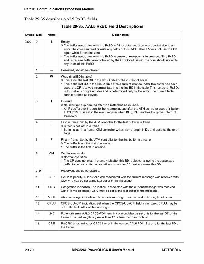
Part IV. Communications Processor Module
Table 29-35 describes AAL5 RxBD Þelds.
Table 29-35. AAL5 RxBD Field Descriptions
Offset Bits Name Description
0x00 0 E Empty. 0 The buffer associated with this RxBD is full or data reception was aborted due to an
error. The core can read or write any Þelds of this RxBD. The CP does not use this BD again while E remains zero.
1 The buffer associated with this RxBD is empty or reception is in progress. This RxBD and its receive buffer are controlled by the CP. Once E is set, the core should not write any Þelds of this RxBD.
1 Ñ Reserved, should be cleared.
2 W Wrap (Þnal BD in table)0 This is not the last BD in the RxBD table of the current channel. 1 This is the last BD in the RxBD table of this current channel. After this buffer has been
used, the CP receives incoming data into the Þrst BD in the table. The number of RxBDs in this table is programmable and is determined only by the W bit. The current table cannot exceed 64 Kbytes.
3 I Interrupt 0 No interrupt is generated after this buffer has been used.1 An Rx buffer event is sent to the interrupt queue after the ATM controller uses this buffer.
FCCE[GINTx] is set in the event register when INT_CNT reaches the global interrupt threshold.
4 L Last in frame. Set by the ATM controller for the last buffer in a frame. 0 Buffer is not last in a frame. 1 Buffer is last in a frame. ATM controller writes frame length in DL and updates the error
ßags.
5 F First in frame. Set by the ATM controller for the Þrst buffer in a frame. 0 The buffer is not the Þrst in a frame. 1 The buffer is the Þrst in a frame.
6 CM Continuous mode0 Normal operation.1 The CP does not clear the empty bit after this BD is closed, allowing the associated
buffer to be overwritten automatically when the CP next accesses this BD.
7Ð9 Ñ Reserved, should be cleared.
10 CLP Cell loss priority. At least one cell associated with the current message was received with CLP = 1. May be set at the last buffer of the message.
11 CNG Congestion indication. The last cell associated with the current message was received with PTI middle bit set. CNG may be set at the last buffer of the message.
12 ABRT Abort message indication. The current message was received with Length Þeld zero.
13 CPUU CPCS-UU+CPI indication. Set when the CPCS-UU+CPI Þeld is non zero. CPUU may be set at the last buffer of the message.
14 LNE Rx length error. AAL5 CPCS-PDU length violation. May be set only for the last BD of the frame if the pad length is greater than 47 or less than zero octets.
15 CRE Rx CRC error. Indicates CRC32 error in the current AAL5 PDU. Set only for the last BD of the frame.
29-70 MPC8260 PowerQUICC II UserÕs Manual MOTOROLA
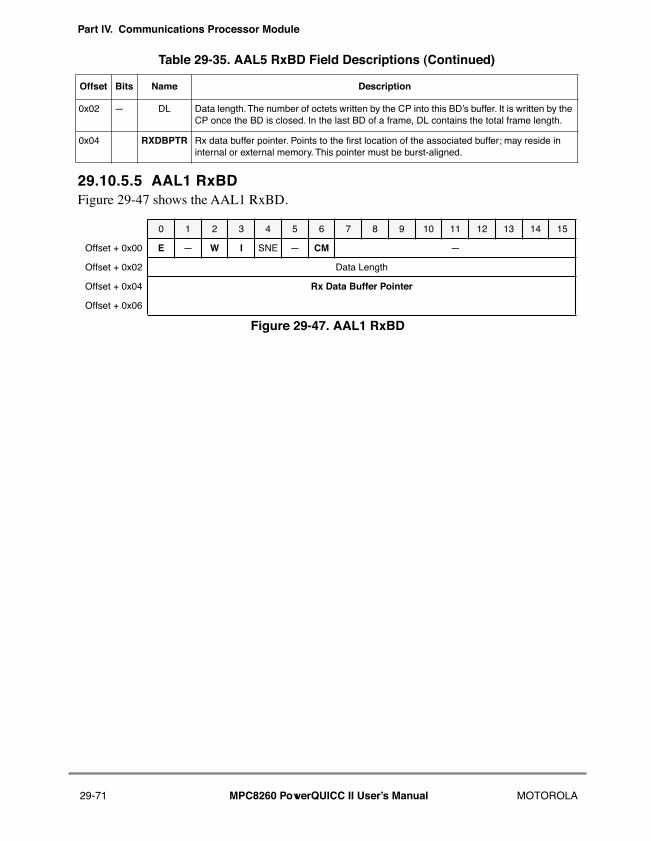
Part IV. Communications Processor Module
29.10.5.5 AAL1 RxBDFigure 29-47 shows the AAL1 RxBD.
0x02 Ñ DL Data length. The number of octets written by the CP into this BDÕs buffer. It is written by the CP once the BD is closed. In the last BD of a frame, DL contains the total frame length.
0x04 RXDBPTR Rx data buffer pointer. Points to the Þrst location of the associated buffer; may reside in internal or external memory. This pointer must be burst-aligned.
0 1 2 3 4 5 6 7 8 9 10 11 12 13 14 15
Offset + 0x00 E Ñ W I SNE Ñ CM Ñ
Offset + 0x02 Data Length
Offset + 0x04 Rx Data Buffer Pointer
Offset + 0x06
Figure 29-47. AAL1 RxBD
Table 29-35. AAL5 RxBD Field Descriptions (Continued)
Offset Bits Name Description
29-71 MPC8260 PowerQUICC II UserÕs Manual MOTOROLA
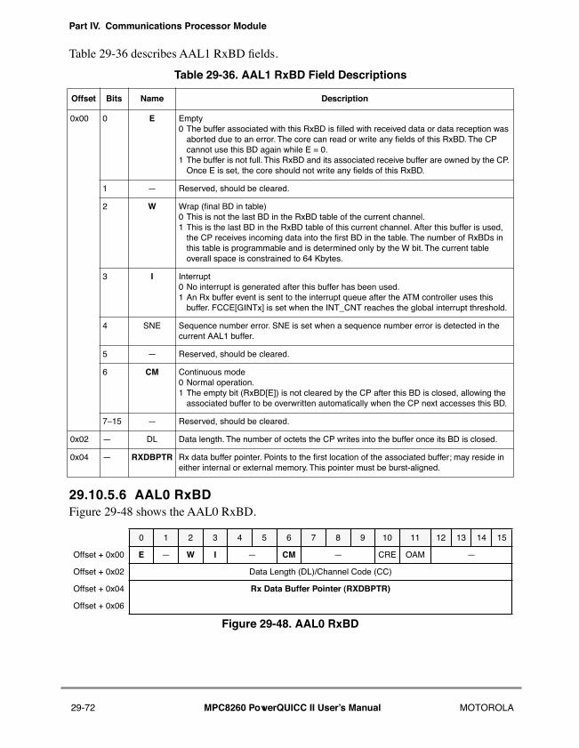
Part IV. Communications Processor Module
Table 29-36 describes AAL1 RxBD Þelds.
29.10.5.6 AAL0 RxBDFigure 29-48 shows the AAL0 RxBD.
Table 29-36. AAL1 RxBD Field Descriptions
Offset Bits Name Description
0x00 0 E Empty0 The buffer associated with this RxBD is Þlled with received data or data reception was
aborted due to an error. The core can read or write any Þelds of this RxBD. The CP cannot use this BD again while E = 0.
1 The buffer is not full. This RxBD and its associated receive buffer are owned by the CP. Once E is set, the core should not write any Þelds of this RxBD.
1 Ñ Reserved, should be cleared.
2 W Wrap (Þnal BD in table)0 This is not the last BD in the RxBD table of the current channel. 1 This is the last BD in the RxBD table of this current channel. After this buffer is used,
the CP receives incoming data into the Þrst BD in the table. The number of RxBDs in this table is programmable and is determined only by the W bit. The current table overall space is constrained to 64 Kbytes.
3 I Interrupt 0 No interrupt is generated after this buffer has been used.1 An Rx buffer event is sent to the interrupt queue after the ATM controller uses this
buffer. FCCE[GINTx] is set when the INT_CNT reaches the global interrupt threshold.
4 SNE Sequence number error. SNE is set when a sequence number error is detected in the current AAL1 buffer.
5 Ñ Reserved, should be cleared.
6 CM Continuous mode0 Normal operation.1 The empty bit (RxBD[E]) is not cleared by the CP after this BD is closed, allowing the
associated buffer to be overwritten automatically when the CP next accesses this BD.
7Ð15 Ñ Reserved, should be cleared.
0x02 Ñ DL Data length. The number of octets the CP writes into the buffer once its BD is closed.
0x04 Ñ RXDBPTR Rx data buffer pointer. Points to the Þrst location of the associated buffer; may reside in either internal or external memory. This pointer must be burst-aligned.
0 1 2 3 4 5 6 7 8 9 10 11 12 13 14 15
Offset + 0x00 E Ñ W I Ñ CM Ñ CRE OAM Ñ
Offset + 0x02 Data Length (DL)/Channel Code (CC)
Offset + 0x04 Rx Data Buffer Pointer (RXDBPTR)
Offset + 0x06
Figure 29-48. AAL0 RxBD
29-72 MPC8260 PowerQUICC II UserÕs Manual MOTOROLA
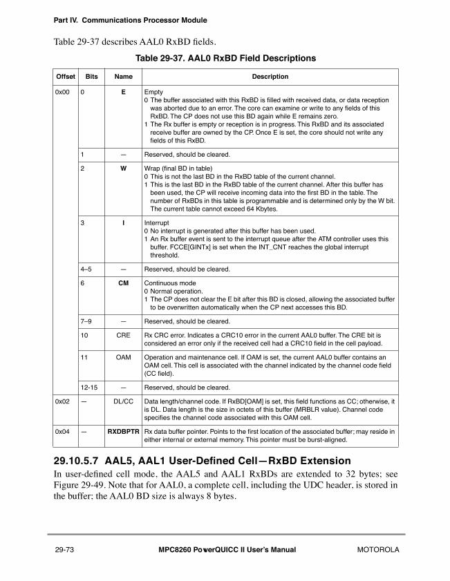
Part IV. Communications Processor Module
Table 29-37 describes AAL0 RxBD Þelds.
29.10.5.7 AAL5, AAL1 User-DeÞned CellÑRxBD ExtensionIn user-deÞned cell mode, the AAL5 and AAL1 RxBDs are extended to 32 bytes; seeFigure 29-49. Note that for AAL0, a complete cell, including the UDC header, is stored inthe buffer; the AAL0 BD size is always 8 bytes.
Table 29-37. AAL0 RxBD Field Descriptions
Offset Bits Name Description
0x00 0 E Empty0 The buffer associated with this RxBD is Þlled with received data, or data reception
was aborted due to an error. The core can examine or write to any Þelds of this RxBD. The CP does not use this BD again while E remains zero.
1 The Rx buffer is empty or reception is in progress. This RxBD and its associated receive buffer are owned by the CP. Once E is set, the core should not write any Þelds of this RxBD.
1 Ñ Reserved, should be cleared.
2 W Wrap (Þnal BD in table)0 This is not the last BD in the RxBD table of the current channel. 1 This is the last BD in the RxBD table of the current channel. After this buffer has
been used, the CP will receive incoming data into the Þrst BD in the table. The number of RxBDs in this table is programmable and is determined only by the W bit. The current table cannot exceed 64 Kbytes.
3 I Interrupt 0 No interrupt is generated after this buffer has been used.1 An Rx buffer event is sent to the interrupt queue after the ATM controller uses this
buffer. FCCE[GINTx] is set when the INT_CNT reaches the global interrupt threshold.
4Ð5 Ñ Reserved, should be cleared.
6 CM Continuous mode0 Normal operation.1 The CP does not clear the E bit after this BD is closed, allowing the associated buffer
to be overwritten automatically when the CP next accesses this BD.
7Ð9 Ñ Reserved, should be cleared.
10 CRE Rx CRC error. Indicates a CRC10 error in the current AAL0 buffer. The CRE bit is considered an error only if the received cell had a CRC10 Þeld in the cell payload.
11 OAM Operation and maintenance cell. If OAM is set, the current AAL0 buffer contains an OAM cell. This cell is associated with the channel indicated by the channel code Þeld (CC Þeld).
12-15 Ñ Reserved, should be cleared.
0x02 Ñ DL/CC Data length/channel code. If RxBD[OAM] is set, this Þeld functions as CC; otherwise, it is DL. Data length is the size in octets of this buffer (MRBLR value). Channel code speciÞes the channel code associated with this OAM cell.
0x04 Ñ RXDBPTR Rx data buffer pointer. Points to the Þrst location of the associated buffer; may reside in either internal or external memory. This pointer must be burst-aligned.
29-73 MPC8260 PowerQUICC II UserÕs Manual MOTOROLA
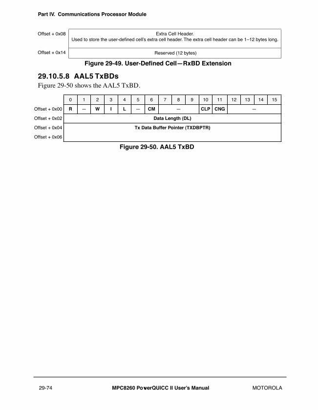
Part IV. Communications Processor Module
29.10.5.8 AAL5 TxBDsFigure 29-50 shows the AAL5 TxBD.
Offset + 0x08 Extra Cell Header. Used to store the user-deÞned cellÕs extra cell header. The extra cell header can be 1Ð12 bytes long.
Offset + 0x14 Reserved (12 bytes)
Figure 29-49. User-Defined CellÑRxBD Extension
0 1 2 3 4 5 6 7 8 9 10 11 12 13 14 15
Offset + 0x00 R Ñ W I L Ñ CM Ñ CLP CNG Ñ
Offset + 0x02 Data Length (DL)
Offset + 0x04 Tx Data Buffer Pointer (TXDBPTR)
Offset + 0x06
Figure 29-50. AAL5 TxBD
29-74 MPC8260 PowerQUICC II UserÕs Manual MOTOROLA
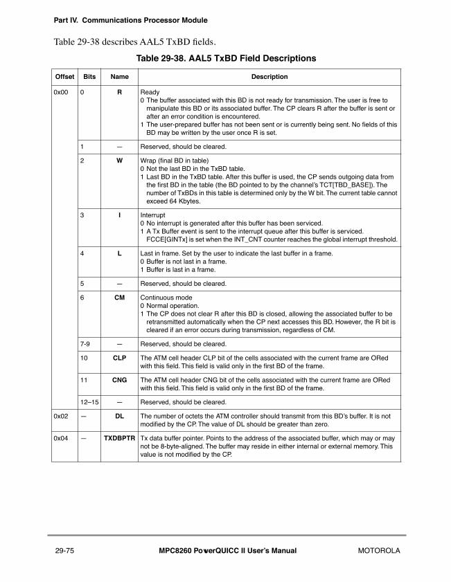
Part IV. Communications Processor Module
Table 29-38 describes AAL5 TxBD Þelds.
Table 29-38. AAL5 TxBD Field Descriptions
Offset Bits Name Description
0x00 0 R Ready0 The buffer associated with this BD is not ready for transmission. The user is free to
manipulate this BD or its associated buffer. The CP clears R after the buffer is sent or after an error condition is encountered.
1 The user-prepared buffer has not been sent or is currently being sent. No Þelds of this BD may be written by the user once R is set.
1 Ñ Reserved, should be cleared.
2 W Wrap (Þnal BD in table)0 Not the last BD in the TxBD table. 1 Last BD in the TxBD table. After this buffer is used, the CP sends outgoing data from
the Þrst BD in the table (the BD pointed to by the channelÕs TCT[TBD_BASE]). The number of TxBDs in this table is determined only by the W bit. The current table cannot exceed 64 Kbytes.
3 I Interrupt 0 No interrupt is generated after this buffer has been serviced. 1 A Tx Buffer event is sent to the interrupt queue after this buffer is serviced.
FCCE[GINTx] is set when the INT_CNT counter reaches the global interrupt threshold.
4 L Last in frame. Set by the user to indicate the last buffer in a frame. 0 Buffer is not last in a frame. 1 Buffer is last in a frame.
5 Ñ Reserved, should be cleared.
6 CM Continuous mode0 Normal operation.1 The CP does not clear R after this BD is closed, allowing the associated buffer to be
retransmitted automatically when the CP next accesses this BD. However, the R bit is cleared if an error occurs during transmission, regardless of CM.
7-9 Ñ Reserved, should be cleared.
10 CLP The ATM cell header CLP bit of the cells associated with the current frame are ORed with this Þeld. This Þeld is valid only in the Þrst BD of the frame.
11 CNG The ATM cell header CNG bit of the cells associated with the current frame are ORed with this Þeld. This Þeld is valid only in the Þrst BD of the frame.
12Ð15 Ñ Reserved, should be cleared.
0x02 Ñ DL The number of octets the ATM controller should transmit from this BDÕs buffer. It is not modiÞed by the CP. The value of DL should be greater than zero.
0x04 Ñ TXDBPTR Tx data buffer pointer. Points to the address of the associated buffer, which may or may not be 8-byte-aligned. The buffer may reside in either internal or external memory. This value is not modiÞed by the CP.
29-75 MPC8260 PowerQUICC II UserÕs Manual MOTOROLA
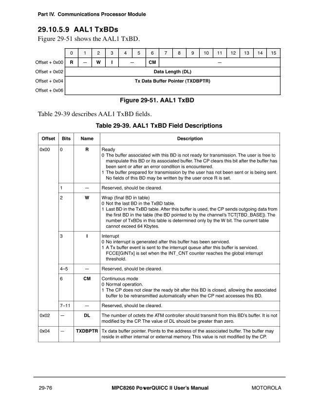
Part IV. Communications Processor Module
29.10.5.9 AAL1 TxBDsFigure 29-51 shows the AAL1 TxBD.
Table 29-39 describes AAL1 TxBD Þelds.
0 1 2 3 4 5 6 7 8 9 10 11 12 13 14 15
Offset + 0x00 R Ñ W I Ñ CM Ñ
Offset + 0x02 Data Length (DL)
Offset + 0x04 Tx Data Buffer Pointer (TXDBPTR)
Offset + 0x06
Figure 29-51. AAL1 TxBD
Table 29-39. AAL1 TxBD Field Descriptions
Offset Bits Name Description
0x00 0 R Ready0 The buffer associated with this BD is not ready for transmission. The user is free to
manipulate this BD or its associated buffer. The CP clears this bit after the buffer has been sent or after an error condition is encountered.
1 The buffer prepared for transmission by the user has not been sent or is being sent. No Þelds of this BD may be written by the user once R is set.
1 Ñ Reserved, should be cleared.
2 W Wrap (Þnal BD in table)0 Not the last BD in the TxBD table. 1 Last BD in the TxBD table. After this buffer is used, the CP sends outgoing data from
the Þrst BD in the table (the BD pointed to by the channelÕs TCT[TBD_BASE]). The number of TxBDs in this table is determined only by the W bit. The current table cannot exceed 64 Kbytes.
3 I Interrupt 0 No interrupt is generated after this buffer has been serviced. 1 A Tx buffer event is sent to the interrupt queue after this buffer is serviced.
FCCE[GINTx] is set when the INT_CNT counter reaches the global interrupt threshold.
4Ð5 Ñ Reserved, should be cleared.
6 CM Continuous mode0 Normal operation.1 The CP does not clear the ready bit after this BD is closed, allowing the associated
buffer to be retransmitted automatically when the CP next accesses this BD.
7Ð11 Ñ Reserved, should be cleared.
0x02 Ñ DL The number of octets the ATM controller should transmit from this BDÕs buffer. It is not modiÞed by the CP. The value of DL should be greater than zero.
0x04 Ñ TXDBPTR Tx data buffer pointer. Points to the address of the associated buffer. The buffer may reside in either internal or external memory. This value is not modiÞed by the CP.
29-76 MPC8260 PowerQUICC II UserÕs Manual MOTOROLA
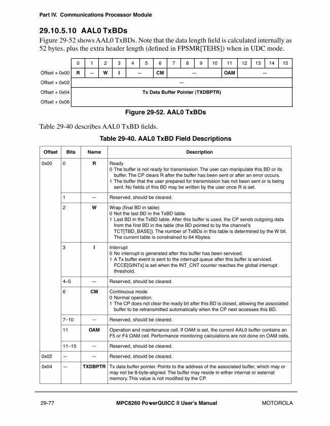
Part IV. Communications Processor Module
29.10.5.10 AAL0 TxBDsFigure 29-52 shows AAL0 TxBDs. Note that the data length Þeld is calculated internally as52 bytes, plus the extra header length (deÞned in FPSMR[TEHS]) when in UDC mode.
Table 29-40 describes AAL0 TxBD Þelds.
0 1 2 3 4 5 6 7 8 9 10 11 12 13 14 15
Offset + 0x00 R Ñ W I Ñ CM Ñ OAM Ñ
Offset + 0x02 Ñ
Offset + 0x04 Tx Data Buffer Pointer (TXDBPTR)
Offset + 0x06
Figure 29-52. AAL0 TxBDs
Table 29-40. AAL0 TxBD Field Descriptions
Offset Bits Name Description
0x00 0 R Ready0 The buffer is not ready for transmission. The user can manipulate this BD or its
buffer. The CP clears R after the buffer has been sent or after an error occurs.1 The buffer that the user prepared for transmission has not been sent or is being
sent. No Þelds of this BD may be written by the user once R is set.
1 Ñ Reserved, should be cleared.
2 W Wrap (Þnal BD in table)0 Not the last BD in the TxBD table. 1 Last BD in the TxBD table. After this buffer is used, the CP sends outgoing data
from the Þrst BD in the table (the BD pointed to by the channelÕs TCT[TBD_BASE]). The number of TxBDs in this table is determined by the W bit. The current table is constrained to 64 Kbytes.
3 I Interrupt 0 No interrupt is generated after this buffer has been serviced. 1 A Tx buffer event is sent to the interrupt queue after this buffer is serviced.
FCCE[GINTx] is set when the INT_CNT counter reaches the global interrupt threshold.
4Ð5 Ñ Reserved, should be cleared.
6 CM Continuous mode0 Normal operation.1 The CP does not clear the ready bit after this BD is closed, allowing the associated
buffer to be retransmitted automatically when the CP next accesses this BD.
7Ð10 Ñ Reserved, should be cleared.
11 OAM Operation and maintenance cell. If OAM is set, the current AAL0 buffer contains an F5 or F4 OAM cell. Performance monitoring calculations are not done on OAM cells.
11Ð15 Ñ Reserved, should be cleared.
0x02 Ñ Ñ Reserved, should be cleared.
0x04 Ñ TXDBPTR Tx data buffer pointer. Points to the address of the associated buffer, which may or may not be 8-byte-aligned. The buffer may reside in either internal or external memory. This value is not modiÞed by the CP.
29-77 MPC8260 PowerQUICC II UserÕs Manual MOTOROLA
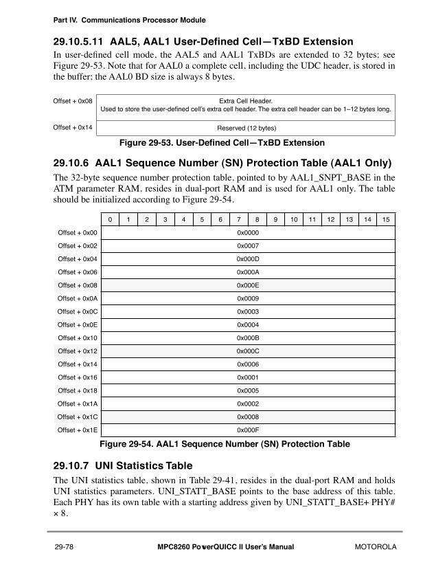
Part IV. Communications Processor Module
29.10.5.11 AAL5, AAL1 User-DeÞned CellÑTxBD ExtensionIn user-deÞned cell mode, the AAL5 and AAL1 TxBDs are extended to 32 bytes; seeFigure 29-53. Note that for AAL0 a complete cell, including the UDC header, is stored inthe buffer; the AAL0 BD size is always 8 bytes.
29.10.6 AAL1 Sequence Number (SN) Protection Table (AAL1 Only)The 32-byte sequence number protection table, pointed to by AAL1_SNPT_BASE in theATM parameter RAM, resides in dual-port RAM and is used for AAL1 only. The tableshould be initialized according to Figure 29-54.
29.10.7 UNI Statistics TableThe UNI statistics table, shown in Table 29-41, resides in the dual-port RAM and holdsUNI statistics parameters. UNI_STATT_BASE points to the base address of this table.Each PHY has its own table with a starting address given by UNI_STATT_BASE+ PHY#´ 8.
Offset + 0x08 Extra Cell Header. Used to store the user-deÞned cellÕs extra cell header. The extra cell header can be 1Ð12 bytes long.
Offset + 0x14 Reserved (12 bytes)
Figure 29-53. User-Defined CellÑTxBD Extension
0 1 2 3 4 5 6 7 8 9 10 11 12 13 14 15
Offset + 0x00 0x0000
Offset + 0x02 0x0007
Offset + 0x04 0x000D
Offset + 0x06 0x000A
Offset + 0x08 0x000E
Offset + 0x0A 0x0009
Offset + 0x0C 0x0003
Offset + 0x0E 0x0004
Offset + 0x10 0x000B
Offset + 0x12 0x000C
Offset + 0x14 0x0006
Offset + 0x16 0x0001
Offset + 0x18 0x0005
Offset + 0x1A 0x0002
Offset + 0x1C 0x0008
Offset + 0x1E 0x000F
Figure 29-54. AAL1 Sequence Number (SN) Protection Table
29-78 MPC8260 PowerQUICC II UserÕs Manual MOTOROLA
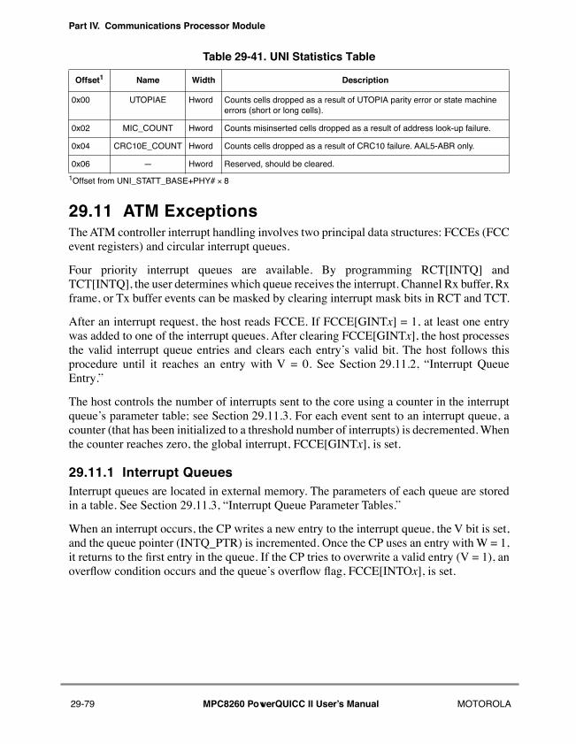
Part IV. Communications Processor Module
29.11 ATM ExceptionsThe ATM controller interrupt handling involves two principal data structures: FCCEs (FCCevent registers) and circular interrupt queues.
Four priority interrupt queues are available. By programming RCT[INTQ] andTCT[INTQ], the user determines which queue receives the interrupt. Channel Rx buffer, Rxframe, or Tx buffer events can be masked by clearing interrupt mask bits in RCT and TCT.
After an interrupt request, the host reads FCCE. If FCCE[GINTx] = 1, at least one entrywas added to one of the interrupt queues. After clearing FCCE[GINTx], the host processesthe valid interrupt queue entries and clears each entryÕs valid bit. The host follows thisprocedure until it reaches an entry with V = 0. See Section 29.11.2, ÒInterrupt QueueEntry.Ó
The host controls the number of interrupts sent to the core using a counter in the interruptqueueÕs parameter table; see Section 29.11.3. For each event sent to an interrupt queue, acounter (that has been initialized to a threshold number of interrupts) is decremented. Whenthe counter reaches zero, the global interrupt, FCCE[GINTx], is set.
29.11.1 Interrupt QueuesInterrupt queues are located in external memory. The parameters of each queue are storedin a table. See Section 29.11.3, ÒInterrupt Queue Parameter Tables.Ó
When an interrupt occurs, the CP writes a new entry to the interrupt queue, the V bit is set,and the queue pointer (INTQ_PTR) is incremented. Once the CP uses an entry with W = 1,it returns to the Þrst entry in the queue. If the CP tries to overwrite a valid entry (V = 1), anoverßow condition occurs and the queueÕs overßow ßag, FCCE[INTOx], is set.
Table 29-41. UNI Statistics Table
Offset1
1Offset from UNI_STATT_BASE+PHY# ´ 8
Name Width Description
0x00 UTOPIAE Hword Counts cells dropped as a result of UTOPIA parity error or state machine errors (short or long cells).
0x02 MIC_COUNT Hword Counts misinserted cells dropped as a result of address look-up failure.
0x04 CRC10E_COUNT Hword Counts cells dropped as a result of CRC10 failure. AAL5-ABR only.
0x06 Ñ Hword Reserved, should be cleared.
29-79 MPC8260 PowerQUICC II UserÕs Manual MOTOROLA
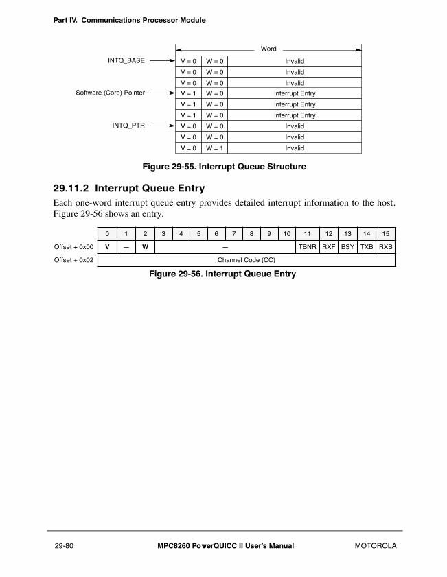
Part IV. Communications Processor Module
Figure 29-55. Interrupt Queue Structure
29.11.2 Interrupt Queue EntryEach one-word interrupt queue entry provides detailed interrupt information to the host.Figure 29-56 shows an entry.
0 1 2 3 4 5 6 7 8 9 10 11 12 13 14 15
Offset + 0x00 V Ñ W Ñ TBNR RXF BSY TXB RXB
Offset + 0x02 Channel Code (CC)
Figure 29-56. Interrupt Queue Entry
V = 0 W = 0 Invalid
V = 0 W = 0 Invalid
V = 0 W = 0 Invalid
V = 1 W = 0 Interrupt Entry
V = 1 W = 0 Interrupt Entry
V = 1 W = 0 Interrupt Entry
V = 0 W = 0 Invalid
V = 0 W = 0 Invalid
V = 0 W = 1 Invalid
INTQ_BASE
Software (Core) Pointer
INTQ_PTR
Word
29-80 MPC8260 PowerQUICC II UserÕs Manual MOTOROLA
Part IV. Communications Processor Module
Table 29-42 describes interrupt queue entry Þelds.
29.11.3 Interrupt Queue Parameter TablesThe interrupt queue parameters are held in parameter tables in the dual-port RAM; seeTable 29-43. INTT_BASE in the parameter RAM points to the base address of these tables.Each of the four interrupt queues has its own parameter table with a starting address givenby INTT_BASE+ RCT/TCT[INTQ] ´ 16.
Table 29-42. Interrupt Queue Entry Field Description
Offset Bits Name Description
0x00 0 V Valid interrupt entry0 This interrupt queue entry is free and can be use by the CP.1 This interrupt queue entry is valid. The host should read this interrupt and clear this bit.
1 Ñ Reserved, should be cleared.
2 W Wrap bit. When set, this is the last interrupt circular table entry. During initialization, the host must clear all W bits in the table except the last one, which must be set.
3Ð10 Ñ Reserved, should be cleared.
11 TBNR Tx buffer-not-ready. Set when a transmit buffer-not-ready interrupt is issued. This interrupt is issued when the CP tries to open a TxBD that is not ready (R = 0). This interrupt is sent only if TCT[BNM] = 1. This interrupt has an associated channel code.Note that for AAL5, this interrupt is sent only if frame transmission is started. In this case, an abort frame transmission is sent (last cell with length=0), the channel is taken out of the APC, and the TCT[VCON] ßag is cleared.
12 RXF Rx frame. RXF is set when an Rx frame interrupt is issued. This interrupt is issued at the end of AAL5 PDU reception. This interrupt is issued only if RCT[RXFM] = 1. This interrupt has an associated channel code.
13 BSY Busy condition. The BD table or the free buffer pool associated with this channel is busy. Cells were discarded due to this condition. This interrupt has an associated channel code.
14 TXB Tx buffer. TXB is set when a transmit buffer interrupt is issued. This interrupt is enabled when both TxBD[I] and TCT[IMK] = 1. This interrupt has an associated channel code.
15 RXB Rx buffer. RXB is set when an Rx buffer interrupt is issued. This interrupt is enabled when both RxBD[I] and RCT[RXBM] = 1. This interrupt has an associated channel code.
0x02 Ñ CC Channel code speciÞes the channel associated with this interrupt.
Table 29-43. Interrupt Queue Parameter Table
Offset 1 Name Width Description
0x00 INTQ_BASE Word Base address of the interrupt queue. User-deÞned.
0x04 INTQ_PTR Word Pointer to interrupt queue entry. Initialize to INTQ_BASE.
0x08 INT_CNT Half Word Interrupt counter. Initialize with INT_ICNT. The CP decrements INT_CNT for each interrupt. When INT_CNT reaches zero, the queueÕs global interrupt ßag FCCE[GINTx] is set.
0x0A INT_ICNT Half Word Interrupt initial count. User-deÞned global interrupt thresholdÑthe number of interrupts required before the CP issues a global interrupt (FCCE[GINTx]).
29-81 MPC8260 PowerQUICC II UserÕs Manual MOTOROLA
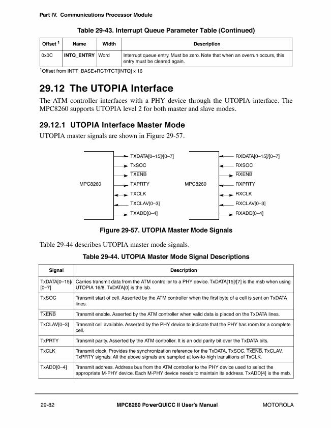
Part IV. Communications Processor Module
29.12 The UTOPIA InterfaceThe ATM controller interfaces with a PHY device through the UTOPIA interface. TheMPC8260 supports UTOPIA level 2 for both master and slave modes.
29.12.1 UTOPIA Interface Master ModeUTOPIA master signals are shown in Figure 29-57.
Figure 29-57. UTOPIA Master Mode Signals
Table 29-44 describes UTOPIA master mode signals.
0x0C INTQ_ENTRY Word Interrupt queue entry. Must be zero. Note that when an overrun occurs, this entry must be cleared again.
1Offset from INTT_BASE+RCT/TCT[INTQ] ´ 16
Table 29-44. UTOPIA Master Mode Signal Descriptions
Signal Description
TxDATA[0Ð15]/[0Ð7]
Carries transmit data from the ATM controller to a PHY device. TxDATA[15]/[7] is the msb when using UTOPIA 16/8, TxDATA[0] is the lsb.
TxSOC Transmit start of cell. Asserted by the ATM controller when the Þrst byte of a cell is sent on TxDATA lines.
TxENB Transmit enable. Asserted by the ATM controller when valid data is placed on the TxDATA lines.
TxCLAV[0Ð3] Transmit cell available. Asserted by the PHY device to indicate that the PHY has room for a complete cell.
TxPRTY Transmit parity. Asserted by the ATM controller. It is an odd parity bit over the TxDATA bits.
TxCLK Transmit clock. Provides the synchronization reference for the TxDATA, TxSOC, TxENB, TxCLAV, TxPRTY signals. All the above signals are sampled at low-to-high transitions of TxCLK.
TxADD[0Ð4] Transmit address. Address bus from the ATM controller to the PHY device used to select the appropriate M-PHY device. Each M-PHY device needs to maintain its address. TxADD[4] is the msb.
Table 29-43. Interrupt Queue Parameter Table (Continued)
Offset 1 Name Width Description
TXDATA[0Ð15]/[0Ð7]
TxSOC
TXENB
TXPRTY
TXCLK
TXCLAV[0Ð3]
TXADD[0Ð4]
MPC8260
RXDATA[0Ð15]/[0Ð7]
RXSOC
RXENB
RXPRTY
RXCLK
RXCLAV[0Ð3]
RXADD[0Ð4]
MPC8260
29-82 MPC8260 PowerQUICC II UserÕs Manual MOTOROLA
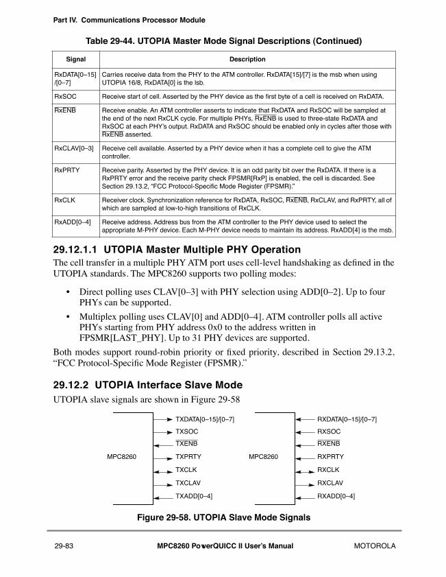
Part IV. Communications Processor Module
29.12.1.1 UTOPIA Master Multiple PHY OperationThe cell transfer in a multiple PHY ATM port uses cell-level handshaking as deÞned in theUTOPIA standards. The MPC8260 supports two polling modes:
¥ Direct polling uses CLAV[0Ð3] with PHY selection using ADD[0Ð2]. Up to four PHYs can be supported.
¥ Multiplex polling uses CLAV[0] and ADD[0Ð4]. ATM controller polls all active PHYs starting from PHY address 0x0 to the address written in FPSMR[LAST_PHY]. Up to 31 PHY devices are supported.
Both modes support round-robin priority or Þxed priority, described in Section 29.13.2,ÒFCC Protocol-SpeciÞc Mode Register (FPSMR).Ó
29.12.2 UTOPIA Interface Slave ModeUTOPIA slave signals are shown in Figure 29-58
Figure 29-58. UTOPIA Slave Mode Signals
RxDATA[0Ð15]/[0Ð7]
Carries receive data from the PHY to the ATM controller. RxDATA[15]/[7] is the msb when using UTOPIA 16/8, RxDATA[0] is the lsb.
RxSOC Receive start of cell. Asserted by the PHY device as the Þrst byte of a cell is received on RxDATA.
RxENB Receive enable. An ATM controller asserts to indicate that RxDATA and RxSOC will be sampled at the end of the next RxCLK cycle. For multiple PHYs, RxENB is used to three-state RxDATA and RxSOC at each PHYÕs output. RxDATA and RxSOC should be enabled only in cycles after those with RxENB asserted.
RxCLAV[0Ð3] Receive cell available. Asserted by a PHY device when it has a complete cell to give the ATM controller.
RxPRTY Receive parity. Asserted by the PHY device. It is an odd parity bit over the RxDATA. If there is a RxPRTY error and the receive parity check FPSMR[RxP] is enabled, the cell is discarded. See Section 29.13.2, ÒFCC Protocol-SpeciÞc Mode Register (FPSMR).Ó
RxCLK Receiver clock. Synchronization reference for RxDATA, RxSOC, RxENB, RxCLAV, and RxPRTY, all of which are sampled at low-to-high transitions of RxCLK.
RxADD[0Ð4] Receive address. Address bus from the ATM controller to the PHY device used to select the appropriate M-PHY device. Each M-PHY device needs to maintain its address. RxADD[4] is the msb.
Table 29-44. UTOPIA Master Mode Signal Descriptions (Continued)
Signal Description
TXDATA[0Ð15]/[0Ð7]
TXSOC
TXENB
TXPRTY
TXCLK
TXCLAV
TXADD[0Ð4]
MPC8260
RXDATA[0Ð15]/[0Ð7]
RXSOC
RXENB
RXPRTY
RXCLK
RXCLAV
RXADD[0Ð4]
MPC8260
29-83 MPC8260 PowerQUICC II UserÕs Manual MOTOROLA
Part IV. Communications Processor Module
Table 29-45 describes UTOPIA slave mode signals.
29.12.2.1 UTOPIA Slave Multiple PHY OperationIn multiple PHY UTOPIA slave mode, cells are transferred using cell-level handshake asdeÞned by the UTOPIA level-2 standard. The user should write the ATM controller PHYaddress in FPSMR[PHY ID].
29.12.2.2 UTOPIA Clocking ModesThe UTOPIA clock is generated by one of the MPC8260Õs baud-rate generators. The usershould assign one of the baud rate generators to supply the UTOPIA clock. See Chapter 15,ÒCPM Multiplexing.Ó
Table 29-45. UTOPIA Slave Mode Signals
Signal Description
TxDATA[0Ð15]/[0Ð7]
Transmit data bus. Carries transmit data from the ATM controller to the master device. TxDATA[15]/[7] is the msb, TxDATA[0] is the lsb.
TxSOC Transmit start of cell. Asserted by an ATM controller as the Þrst byte of a cell is sent on the TxDATA lines.
TxENB Transmit enable. An input to the ATM controller. It is asserted by the UTOPIA master to signal the slave to send data in the next TxCLK cycle.
TxCLAV Transmit cell available. Asserted by the ATM controller to indicate it has a complete cell to transmit.
TxPRTY Transmit parity. Asserted by the ATM controller. It is an odd parity bit over the TxDATA.
TxCLK Transmit clock. Provides the synchronization reference for the TxDATA, TxSOC, TxENB, TxCLAV, and TxPRTY signals. All of the above signals are sampled at low-to-high transitions of TxCLK.
TxADD[0Ð4] Transmit address. Address bus from the master to the ATM controller used to select the appropriate M-PHY device.
RxDATA[0Ð15]/[0Ð7]
Receive data bus. Carries receive data from the master to the ATM controller. RxDATA[15]/[7] is the msb, RxDATA[0] is the lsb.
RxSOC Receive start of cell. Asserted by the master device whenever the Þrst byte of a cell is being received on the RxDATA lines.
RxENB Receive enable. Asserted by the master device to signal the slave to sample the RxDATA and RxSOC signals.
RxCLAV Receive cell available. Asserted by the ATM controller to indicate it can receive a complete cell.
RxPRTY Receive parity. Asserted by the PHY device. It is an odd parity bit over the RxDATA[0Ð15]. If there is a RxPRTY error and the receive parity check FPSMR[RxP] is enabled, the cell is discarded. See see Section 29.13.2, ÒFCC Protocol-SpeciÞc Mode Register (FPSMR).Ó
RxCLK Receive clock. Provides the synchronization reference for the RxDATA, RxSOC, RxENB, RxCLAV, and RxPRTY signals. All the above signals are sampled at low-to-high transitions of RxCLK.
RxADD[0Ð4] Receive address. Address bus from master to the ATM controller device used to select the appropriate M-PHY device.
29-84 MPC8260 PowerQUICC II UserÕs Manual MOTOROLA
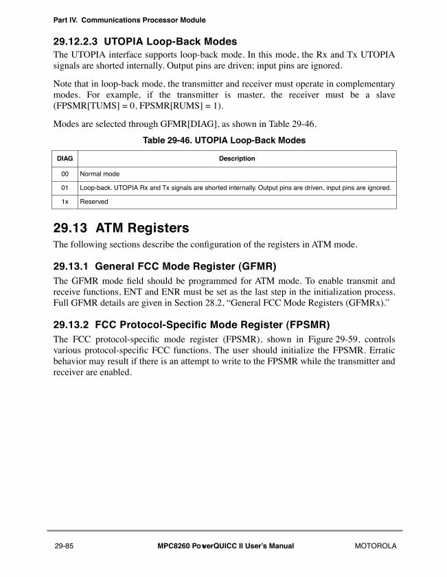
Part IV. Communications Processor Module
29.12.2.3 UTOPIA Loop-Back ModesThe UTOPIA interface supports loop-back mode. In this mode, the Rx and Tx UTOPIAsignals are shorted internally. Output pins are driven; input pins are ignored.
Note that in loop-back mode, the transmitter and receiver must operate in complementarymodes. For example, if the transmitter is master, the receiver must be a slave(FPSMR[TUMS] = 0, FPSMR[RUMS] = 1).
Modes are selected through GFMR[DIAG], as shown in Table 29-46.
29.13 ATM RegistersThe following sections describe the conÞguration of the registers in ATM mode.
29.13.1 General FCC Mode Register (GFMR)The GFMR mode Þeld should be programmed for ATM mode. To enable transmit andreceive functions, ENT and ENR must be set as the last step in the initialization process.Full GFMR details are given in Section 28.2, ÒGeneral FCC Mode Registers (GFMRx).Ó
29.13.2 FCC Protocol-SpeciÞc Mode Register (FPSMR)The FCC protocol-speciÞc mode register (FPSMR), shown in Figure 29-59, controlsvarious protocol-speciÞc FCC functions. The user should initialize the FPSMR. Erraticbehavior may result if there is an attempt to write to the FPSMR while the transmitter andreceiver are enabled.
Table 29-46. UTOPIA Loop-Back Modes
DIAG Description
00 Normal mode
01 Loop-back. UTOPIA Rx and Tx signals are shorted internally. Output pins are driven, input pins are ignored.
1x Reserved
29-85 MPC8260 PowerQUICC II UserÕs Manual MOTOROLA
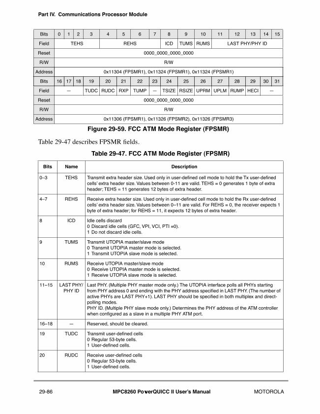
Part IV. Communications Processor Module
Table 29-47 describes FPSMR Þelds.
Bits 0 1 2 3 4 5 6 7 8 9 10 11 12 13 14 15
Field TEHS REHS ICD TUMS RUMS LAST PHY/PHY ID
Reset 0000_0000_0000_0000
R/W R/W
Address 0x11304 (FPSMR1), 0x11324 (FPSMR1), 0x11324 (FPSMR1)
Bits 16 17 18 19 20 21 22 23 24 25 26 27 28 29 30 31
Field Ñ TUDC RUDC RXP TUMP Ñ TSIZE RSIZE UPRM UPLM RUMP HECI Ñ
Reset 0000_0000_0000_0000
R/W R/W
Address 0x11306 (FPSMR1), 0x11326 (FPSMR2), 0x11326 (FPSMR3)
Figure 29-59. FCC ATM Mode Register (FPSMR)
Table 29-47. FCC ATM Mode Register (FPSMR)
Bits Name Description
0Ð3 TEHS Transmit extra header size. Used only in user-deÞned cell mode to hold the Tx user-deÞned cellsÕ extra header size. Values between 0-11 are valid. TEHS = 0 generates 1 byte of extra header; TEHS = 11 generates 12 bytes of extra header.
4Ð7 REHS Receive extra header size. Used only in user-deÞned cell mode to hold the Rx user-deÞned cellsÕ extra header size. Values between 0Ð11 are valid. For REHS = 0, the receiver expects 1 byte of extra header; for REHS = 11, it expects 12 bytes of extra header.
8 ICD Idle cells discard0 Discard idle cells (GFC, VPI, VCI, PTI =0).1 Do not discard idle cells.
9 TUMS Transmit UTOPIA master/slave mode0 Transmit UTOPIA master mode is selected.1 Transmit UTOPIA slave mode is selected.
10 RUMS Receive UTOPIA master/slave mode0 Receive UTOPIA master mode is selected.1 Receive UTOPIA slave mode is selected.
11Ð15 LAST PHY/ PHY ID
Last PHY. (Multiple PHY master mode only.) The UTOPIA interface polls all PHYs starting from PHY address 0 and ending with the PHY address speciÞed in LAST PHY. (The number of active PHYs are LAST PHY+1). LAST PHY should be speciÞed in both multiplex and direct-polling modes.PHY ID. (Multiple PHY slave mode only.) Determines the PHY address of the ATM controller when conÞgured as a slave in a multiple PHY ATM port.
16Ð18 Ñ Reserved, should be cleared.
19 TUDC Transmit user-deÞned cells0 Regular 53-byte cells.1 User-deÞned cells.
20 RUDC Receive user-deÞned cells0 Regular 53-byte cells.1 User-deÞned cells.
29-86 MPC8260 PowerQUICC II UserÕs Manual MOTOROLA
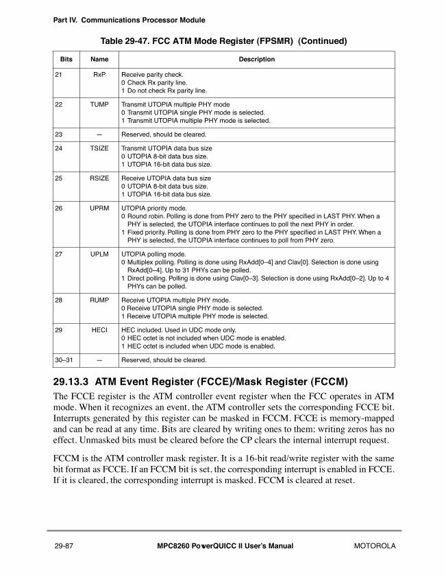
Part IV. Communications Processor Module
29.13.3 ATM Event Register (FCCE)/Mask Register (FCCM)The FCCE register is the ATM controller event register when the FCC operates in ATMmode. When it recognizes an event, the ATM controller sets the corresponding FCCE bit.Interrupts generated by this register can be masked in FCCM. FCCE is memory-mappedand can be read at any time. Bits are cleared by writing ones to them; writing zeros has noeffect. Unmasked bits must be cleared before the CP clears the internal interrupt request.
FCCM is the ATM controller mask register. It is a 16-bit read/write register with the samebit format as FCCE. If an FCCM bit is set, the corresponding interrupt is enabled in FCCE.If it is cleared, the corresponding interrupt is masked. FCCM is cleared at reset.
21 RxP Receive parity check.0 Check Rx parity line.1 Do not check Rx parity line.
22 TUMP Transmit UTOPIA multiple PHY mode0 Transmit UTOPIA single PHY mode is selected.1 Transmit UTOPIA multiple PHY mode is selected.
23 Ñ Reserved, should be cleared.
24 TSIZE Transmit UTOPIA data bus size0 UTOPIA 8-bit data bus size.1 UTOPIA 16-bit data bus size.
25 RSIZE Receive UTOPIA data bus size0 UTOPIA 8-bit data bus size.1 UTOPIA 16-bit data bus size.
26 UPRM UTOPIA priority mode.0 Round robin. Polling is done from PHY zero to the PHY speciÞed in LAST PHY. When a
PHY is selected, the UTOPIA interface continues to poll the next PHY in order.1 Fixed priority. Polling is done from PHY zero to the PHY speciÞed in LAST PHY. When a
PHY is selected, the UTOPIA interface continues to poll from PHY zero.
27 UPLM UTOPIA polling mode.0 Multiplex polling. Polling is done using RxAdd[0Ð4] and Clav[0]. Selection is done using
RxAdd[0Ð4]. Up to 31 PHYs can be polled.1 Direct polling. Polling is done using Clav[0Ð3]. Selection is done using RxAdd[0Ð2]. Up to 4
PHYs can be polled.
28 RUMP Receive UTOPIA multiple PHY mode.0 Receive UTOPIA single PHY mode is selected.1 Receive UTOPIA multiple PHY mode is selected.
29 HECI HEC included. Used in UDC mode only.0 HEC octet is not included when UDC mode is enabled.1 HEC octet is included when UDC mode is enabled.
30Ð31 Ñ Reserved, should be cleared.
Table 29-47. FCC ATM Mode Register (FPSMR) (Continued)
Bits Name Description
29-87 MPC8260 PowerQUICC II UserÕs Manual MOTOROLA
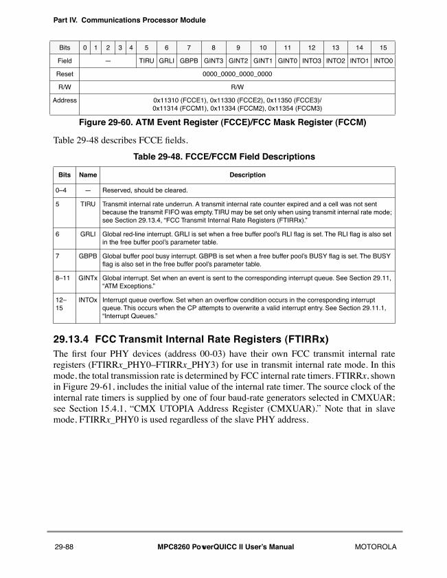
Part IV. Communications Processor Module
Table 29-48 describes FCCE Þelds.
29.13.4 FCC Transmit Internal Rate Registers (FTIRRx)The Þrst four PHY devices (address 00-03) have their own FCC transmit internal rateregisters (FTIRRx_PHY0ÐFTIRRx_PHY3) for use in transmit internal rate mode. In thismode, the total transmission rate is determined by FCC internal rate timers. FTIRRx, shownin Figure 29-61, includes the initial value of the internal rate timer. The source clock of theinternal rate timers is supplied by one of four baud-rate generators selected in CMXUAR;see Section 15.4.1, ÒCMX UTOPIA Address Register (CMXUAR).Ó Note that in slavemode, FTIRRx_PHY0 is used regardless of the slave PHY address.
Bits 0 1 2 3 4 5 6 7 8 9 10 11 12 13 14 15
Field Ñ TIRU GRLI GBPB GINT3 GINT2 GINT1 GINT0 INTO3 INTO2 INTO1 INTO0
Reset 0000_0000_0000_0000
R/W R/W
Address 0x11310 (FCCE1), 0x11330 (FCCE2), 0x11350 (FCCE3)/0x11314 (FCCM1), 0x11334 (FCCM2), 0x11354 (FCCM3)
Figure 29-60. ATM Event Register (FCCE)/FCC Mask Register (FCCM)
Table 29-48. FCCE/FCCM Field Descriptions
Bits Name Description
0Ð4 Ñ Reserved, should be cleared.
5 TIRU Transmit internal rate underrun. A transmit internal rate counter expired and a cell was not sent because the transmit FIFO was empty. TIRU may be set only when using transmit internal rate mode; see Section 29.13.4, ÒFCC Transmit Internal Rate Registers (FTIRRx).Ó
6 GRLI Global red-line interrupt. GRLI is set when a free buffer poolÕs RLI ßag is set. The RLI ßag is also set in the free buffer poolÕs parameter table.
7 GBPB Global buffer pool busy interrupt. GBPB is set when a free buffer poolÕs BUSY ßag is set. The BUSY ßag is also set in the free buffer poolÕs parameter table.
8Ð11 GINTx Global interrupt. Set when an event is sent to the corresponding interrupt queue. See Section 29.11, ÒATM Exceptions.Ó
12Ð15
INTOx Interrupt queue overßow. Set when an overßow condition occurs in the corresponding interrupt queue. This occurs when the CP attempts to overwrite a valid interrupt entry. See Section 29.11.1, ÒInterrupt Queues.Ó
29-88 MPC8260 PowerQUICC II UserÕs Manual MOTOROLA
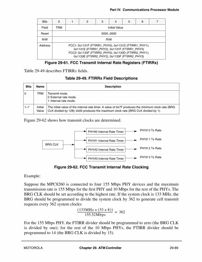
Part IV. Communications Processor Module
Table 29-49 describes FTIRRx Þelds.
Figure 29-62 shows how transmit clocks are determined. .
Figure 29-62. FCC Transmit Internal Rate Clocking
Example:
Suppose the MPC8260 is connected to four 155 Mbps PHY devices and the maximumtransmission rate is 155 Mbps for the Þrst PHY and 10 Mbps for the rest of the PHYs. TheBRG CLK should be set according to the highest rate. If the system clock is 133 MHz, theBRG should be programmed to divide the system clock by 362 to generate cell transmitrequests every 362 system clocks:
For the 155 Mbps PHY, the FTIRR divider should be programmed to zero (the BRG CLKis divided by one); for the rest of the 10 Mbps PHYs, the FTIRR divider should beprogrammed to 14 (the BRG CLK is divided by 15).
Bits 0 1 2 3 4 5 6 7
Field TRM Initial Value
Reset 0000_0000
R/W R/W
Address FCC1: 0x1131F (FTIRR1_PHY0), 0x1131D (FTIRR1_PHY1),0x1131E (FTIRR1_PHY2), 0x1131F (FTIRR1_PHY3)
FCC2: 0x1133F (FTIRR2_PHY0), 0x1133D (FTIRR2_PHY1),0x1133E (FTIRR2_PHY2), 0x1133F (FTIRR2_PHY3)
Figure 29-61. FCC Transmit Internal Rate Registers (FTIRRx)
Table 29-49. FTIRRx Field Descriptions
Bits Name Description
0 TRM Transmit mode.0 External rate mode.1 Internal rate mode.
1Ð7 Initial Value
The initial value of the internal rate timer. A value of 0x7F produces the minimum clock rate (BRG CLK divided by 128); 0x00 produces the maximum clock rate (BRG CLK divided by 1).
BRG CLK
PHY#0 Internal Rate Timer PHY# 0 Tx Rate
PHY# 1 Tx Rate
PHY# 2 Tx Rate
PHY# 3 Tx RatePHY#3 Internal Rate Timer
PHY#2 Internal Rate Timer
PHY#1 Internal Rate Timer
133MHz 53 8´( )´( )155.52Mbps
----------------------------------------------------- 362=
MOTOROLA Chapter 29. ATM Controller 29-89
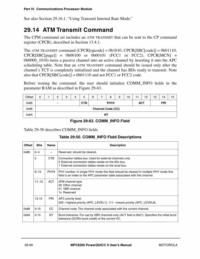
Part IV. Communications Processor Module
See also Section 29.16.1, ÒUsing Transmit Internal Rate Mode.Ó
29.14 ATM Transmit CommandThe CPM command set includes an ATM TRANSMIT that can be sent to the CP commandregister (CPCR), described in Section 13.4.1.
The ATM TRANSMIT command (CPCR[opcode] = 0b1010, CPCR[SBC[code]] = 0b01110,CPCR[SBC[page]] = 0b00100 or 0b00101 (FCC1 or FCC2), CPCR[MCN] =0b0000_1010) turns a passive channel into an active channel by inserting it into the APCscheduling table. Note that an ATM TRANSMIT command should be issued only after thechannelÕs TCT is completely initialized and the channel has BDs ready to transmit. Notealso that CPCR[SBC[code]] = 0b01110 and not FCC1 or FCC2 code.
Before issuing the command, the user should initialize COMM_INFO Þelds in theparameter RAM as described in Figure 29-63.
Table 29-50 describes COMM_INFO Þelds
Offset 0 1 2 3 4 5 6 7 8 9 10 11 12 13 14 15
0x86 Ñ CTB PHY# ACT PRI
0x88 Channel Code (CC)
0x8A BT
Figure 29-63. COMM_INFO Field
Table 29-50. COMM_INFO Field Descriptions
Offset Bits Name Description
0x86 0Ð4 Ñ Reserved, should be cleared.
5 CTB Connection tables bus. Used for external channels only0 External connection tables reside on the 60x bus.1 External connection tables reside on the local bus.
6Ð10 PHY# PHY number. In single PHY mode this Þeld should be cleared In multiple PHY mode this Þeld is an index to the APC parameter table associated with this channel.
11Ð12 ACT ATM channel type00 Other channel01 VBR channel1x Reserved
13-15 PRI APC priority level.000Ñhighest priority (APC_LEVEL1), 111Ñlowest priority (APC_LEVEL8).
0x88 0-15 CC Channel code. The channel code associated with the current channel.
0x8A 0-15 BT Burst tolerance. For use by VBR channels only (ACT Þeld is 0b01). SpeciÞes the initial burst tolerance (GCRA burst credit) of the current VC.
29-90 MPC8260 PowerQUICC II UserÕs Manual MOTOROLA
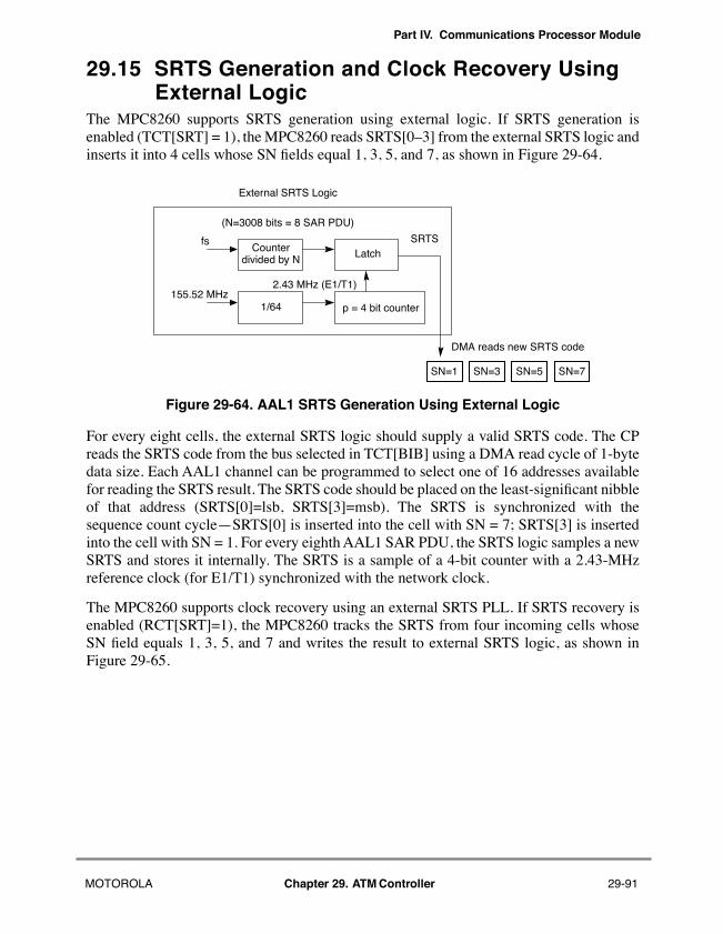
Part IV. Communications Processor Module
29.15 SRTS Generation and Clock Recovery Using External Logic
The MPC8260 supports SRTS generation using external logic. If SRTS generation isenabled (TCT[SRT] = 1), the MPC8260 reads SRTS[0Ð3] from the external SRTS logic andinserts it into 4 cells whose SN Þelds equal 1, 3, 5, and 7, as shown in Figure 29-64.
Figure 29-64. AAL1 SRTS Generation Using External Logic
For every eight cells, the external SRTS logic should supply a valid SRTS code. The CPreads the SRTS code from the bus selected in TCT[BIB] using a DMA read cycle of 1-bytedata size. Each AAL1 channel can be programmed to select one of 16 addresses availablefor reading the SRTS result. The SRTS code should be placed on the least-signiÞcant nibbleof that address (SRTS[0]=lsb, SRTS[3]=msb). The SRTS is synchronized with thesequence count cycleÑSRTS[0] is inserted into the cell with SN = 7; SRTS[3] is insertedinto the cell with SN = 1. For every eighth AAL1 SAR PDU, the SRTS logic samples a newSRTS and stores it internally. The SRTS is a sample of a 4-bit counter with a 2.43-MHzreference clock (for E1/T1) synchronized with the network clock.
The MPC8260 supports clock recovery using an external SRTS PLL. If SRTS recovery isenabled (RCT[SRT]=1), the MPC8260 tracks the SRTS from four incoming cells whoseSN Þeld equals 1, 3, 5, and 7 and writes the result to external SRTS logic, as shown inFigure 29-65.
p = 4 bit counter1/64155.52 MHz
2.43 MHz (E1/T1)
Latchfs
Counterdivided by N
(N=3008 bits = 8 SAR PDU)
SRTS
External SRTS Logic
SN=1 SN=3 SN=5 SN=7
DMA reads new SRTS code
MOTOROLA Chapter 29. ATM Controller 29-91
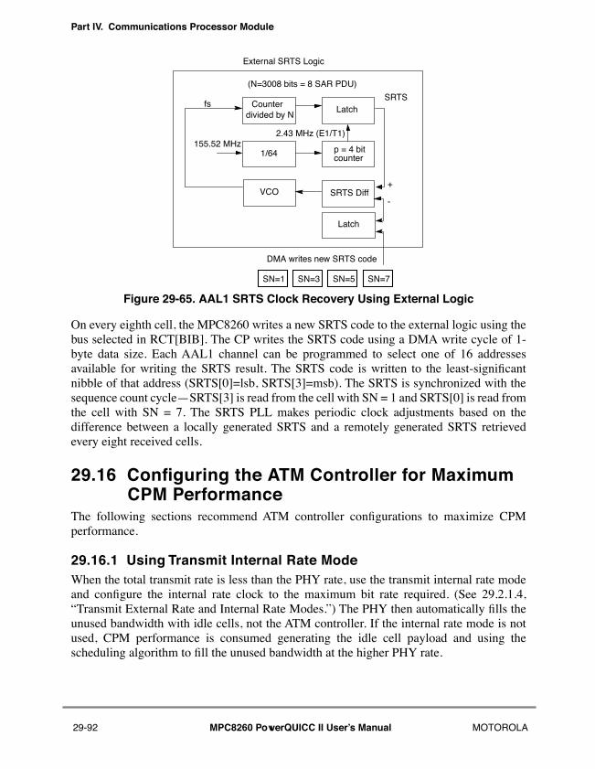
Part IV. Communications Processor Module
Figure 29-65. AAL1 SRTS Clock Recovery Using External Logic
On every eighth cell, the MPC8260 writes a new SRTS code to the external logic using thebus selected in RCT[BIB]. The CP writes the SRTS code using a DMA write cycle of 1-byte data size. Each AAL1 channel can be programmed to select one of 16 addressesavailable for writing the SRTS result. The SRTS code is written to the least-signiÞcantnibble of that address (SRTS[0]=lsb, SRTS[3]=msb). The SRTS is synchronized with thesequence count cycleÑSRTS[3] is read from the cell with SN = 1 and SRTS[0] is read fromthe cell with SN = 7. The SRTS PLL makes periodic clock adjustments based on thedifference between a locally generated SRTS and a remotely generated SRTS retrievedevery eight received cells.
29.16 ConÞguring the ATM Controller for Maximum CPM Performance
The following sections recommend ATM controller conÞgurations to maximize CPMperformance.
29.16.1 Using Transmit Internal Rate ModeWhen the total transmit rate is less than the PHY rate, use the transmit internal rate modeand conÞgure the internal rate clock to the maximum bit rate required. (See 29.2.1.4,ÒTransmit External Rate and Internal Rate Modes.Ó) The PHY then automatically Þlls theunused bandwidth with idle cells, not the ATM controller. If the internal rate mode is notused, CPM performance is consumed generating the idle cell payload and using thescheduling algorithm to Þll the unused bandwidth at the higher PHY rate.
p = 4 bit1/64155.52 MHz
2.43 MHz (E1/T1)
Latchfs Counter
divided by N
(N=3008 bits = 8 SAR PDU)
SRTS
External SRTS Logic
SRTS Diff+
-VCO
SN=1 SN=3 SN=5 SN=7
DMA writes new SRTS code
Latch
counter
29-92 MPC8260 PowerQUICC II UserÕs Manual MOTOROLA
Part IV. Communications Processor Module
For example, suppose a system uses a 155.52-Mbps OC-3 device as PHY0, but themaximum required data rate is only 100 Mbps. In transmit internal rate mode, the user canconÞgure the internal rate mechanism to clock the ATM transmitter at a cell rate of 100Mbps. If the system clock is 133 MHz, program a BRG to divide the system clock by 563to generate a transmit cell request every 563 CPM clocks:
Set FTIRRx_PHY0[TRM] to enable the transmit internal rate mode and clearFTIRRx_PHY0[Initial Value] since there is no need to further divide the BRG. SeeSection 29.13.4, ÒFCC Transmit Internal Rate Registers (FTIRRx).Ó
In external rate mode, however, the transmit cell request frequency is determined by thePHYÕs maximum rate, not by internal FCC counters. If an OC-3 PHY is used with the ATMcontroller in external rate mode, the requests must be generated every 362 CPM clocks(assuming a 133-MHz CPM clock). If only 100 Mbps is used for real data, 36% of thetransmit cell requests consume CPM processing time sending idle cells.
29.16.2 APC ConÞgurationMaximizing the number of cells per slot (CPS) and minimizing the priority levels deÞnedin the APC data structure improves CPM performance:
¥ Cells per slot. CPS deÞnes the maximum number of ATM cells allowed to be sent during a time slot. (See Section 29.3.3.1, ÒDetermining the Cells Per Slot (CPS) in a Scheduling Table.Ó) The scheduling algorithm is more efÞcient sending multiple cells per time slot using the linked-channel Þeld. Therefore, choose the maximum number of cells per slot allowed by the application.
¥ Priority levels. The user can conÞgure the APC data structure to have from one to eight priority levels. (See Section 29.3.6, ÒDetermining the Priority of an ATM Channel.Ó) For each time slot, the scheduling algorithm scans all priority levels and maintains pointers for each level. Therefore, enable only the minimum number of priority levels required.
29.16.3 Buffer ConÞgurationUsing statically allocated buffers of optimal sizes also improves CPM performance:
¥ Buffer size. Opening and closing buffer descriptors consumes CPM processing time. Because smaller buffers require more opening and closing of BDs, the optimal buffer size for maximum CPM performance is equal to the packet size (an AAL5 frame, for example).
¥ Free buffer pool. When the free buffer pool is used, the CPM dynamically allocates buffers and links them to a channelÕs BD. In static buffer allocation, the core assigns a Þxed data buffer to each BD. (See Section 29.10.5.2, ÒReceive Buffers Operation.Ó) When allowed by the application, use static buffer allocation to increase CPM performance.
133MHz 53 8´( )´( )100Mbps
----------------------------------------------------- 563=
MOTOROLA Chapter 29. ATM Controller 29-93

Part IV. Communications Processor Module
29-94 MPC8260 PowerQUICC II UserÕs Manual MOTOROLA
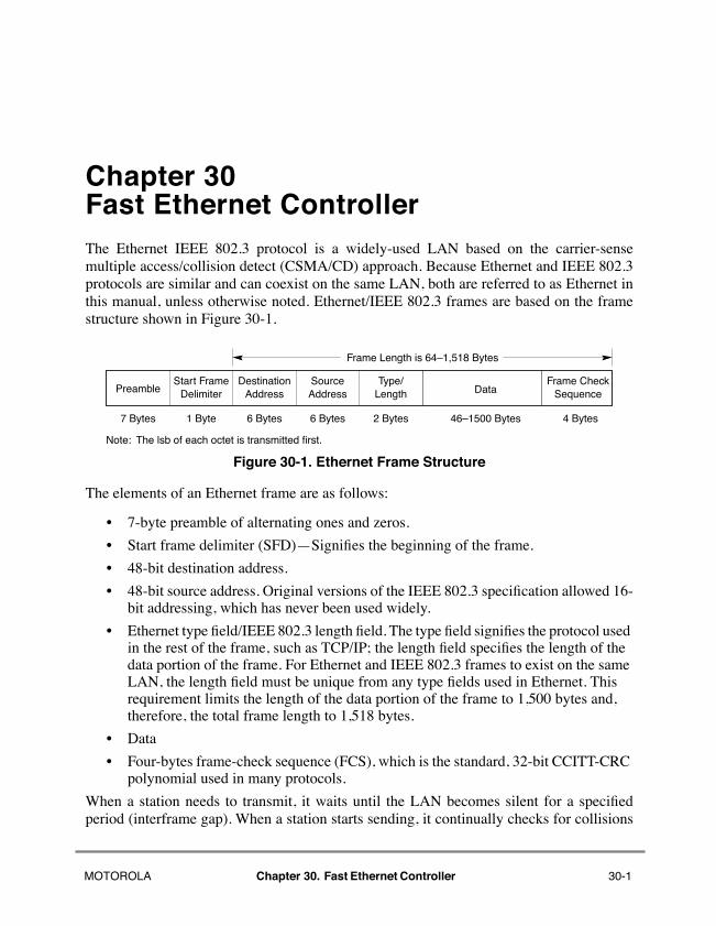
Chapter 30 Fast Ethernet Controller300300
The Ethernet IEEE 802.3 protocol is a widely-used LAN based on the carrier-sensemultiple access/collision detect (CSMA/CD) approach. Because Ethernet and IEEE 802.3protocols are similar and can coexist on the same LAN, both are referred to as Ethernet inthis manual, unless otherwise noted. Ethernet/IEEE 802.3 frames are based on the framestructure shown in Figure 30-1.
Figure 30-1. Ethernet Frame Structure
The elements of an Ethernet frame are as follows:
¥ 7-byte preamble of alternating ones and zeros.
¥ Start frame delimiter (SFD)ÑSigniÞes the beginning of the frame.
¥ 48-bit destination address.
¥ 48-bit source address. Original versions of the IEEE 802.3 speciÞcation allowed 16-bit addressing, which has never been used widely.
¥ Ethernet type Þeld/IEEE 802.3 length Þeld. The type Þeld signiÞes the protocol used in the rest of the frame, such as TCP/IP; the length Þeld speciÞes the length of the data portion of the frame. For Ethernet and IEEE 802.3 frames to exist on the same LAN, the length Þeld must be unique from any type Þelds used in Ethernet. This requirement limits the length of the data portion of the frame to 1,500 bytes and, therefore, the total frame length to 1,518 bytes.
¥ Data
¥ Four-bytes frame-check sequence (FCS), which is the standard, 32-bit CCITT-CRC polynomial used in many protocols.
When a station needs to transmit, it waits until the LAN becomes silent for a speciÞedperiod (interframe gap). When a station starts sending, it continually checks for collisions
PreambleStart Frame
DataDelimiterDestination
AddressType/
LengthSourceAddress
Frame CheckSequence
7 Bytes 1 Byte 6 Bytes 6 Bytes 2 Bytes 46Ð1500 Bytes 4 Bytes
Frame Length is 64Ð1,518 Bytes
Note: The lsb of each octet is transmitted first.
MOTOROLA Chapter 30. Fast Ethernet Controller 30-1
Part IV. Communications Processor Module
on the LAN. If a collision is detected, the station forces a jam signal (all ones) on its frameand stops transmitting. Collisions usually occur close to the beginning of a frame. Thestation then waits a random time period (backoff) before attempting to send again. Whenthe backoff completes, the station waits for silence on the LAN and then beginsretransmission on the LAN. This process is called a retry. If the frame is not successfullysent within 15 retries, an error is indicated.
10-Mbps Ethernet basic timing speciÞcations follow:
¥ Transmits at 0.8 µs per byte
¥ The preamble plus start frame delimiter is sent in 6.4 µs.
¥ The minimum interframe gap is 9.6 µs.
¥ The slot time is 51.2 µs.
100-Mbps Ethernet basic timing speciÞcations follow:
¥ Transmits at 0.08 µs per byte
¥ The preamble plus start frame delimiter is sent in 0.64 µs.
¥ The minimum interframe gap is 0.96 µs.
¥ The slot time is 5.12 µs.
30.1 Fast Ethernet on the MPC8260When a general FCC mode register (GFMRx[MODE]) selects Ethernet protocol, that FCCperforms the full set of IEEE 802.3/Ethernet CSMA/CD media access control (MAC) andchannel interface functions. Figure 30-2 shows a block diagram of the FCC Ethernetcontrol logic.
30-2 MPC8260 PowerQUICC II UserÕs Manual MOTOROLA
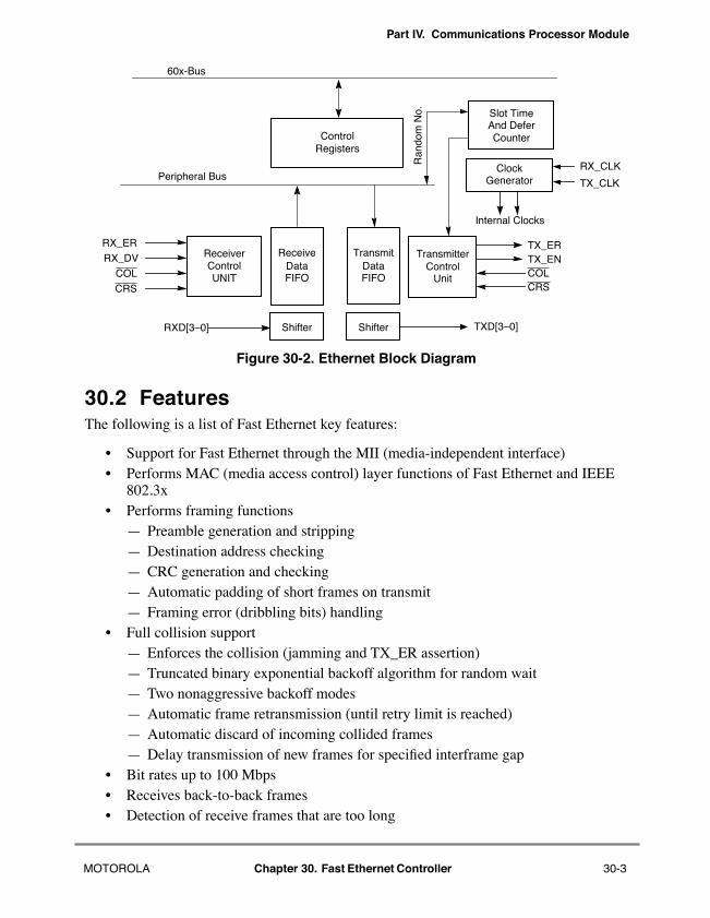
Part IV. Communications Processor Module
Figure 30-2. Ethernet Block Diagram
30.2 FeaturesThe following is a list of Fast Ethernet key features:
¥ Support for Fast Ethernet through the MII (media-independent interface)¥ Performs MAC (media access control) layer functions of Fast Ethernet and IEEE
802.3x¥ Performs framing functions
Ñ Preamble generation and strippingÑ Destination address checkingÑ CRC generation and checkingÑ Automatic padding of short frames on transmitÑ Framing error (dribbling bits) handling
¥ Full collision supportÑ Enforces the collision (jamming and TX_ER assertion)Ñ Truncated binary exponential backoff algorithm for random waitÑ Two nonaggressive backoff modesÑ Automatic frame retransmission (until retry limit is reached)Ñ Automatic discard of incoming collided framesÑ Delay transmission of new frames for speciÞed interframe gap
¥ Bit rates up to 100 Mbps¥ Receives back-to-back frames¥ Detection of receive frames that are too long
Shifter
ReceiveReceiverControlUNIT FIFO
Shifter
Transmit TransmitterControl
UnitFIFO
Slot Time
ClockGenerator
Internal Clocks
ControlRegisters
TXD[3Ð0]RXD[3Ð0]
Peripheral Bus
60x-Bus
DataData
RX_CLK
TX_CLK
And DeferCounter
TX_ER
Ran
dom
No.
CRSCRS
COL
RX_ER
TX_ENCOL
RX_DV
MOTOROLA Chapter 30. Fast Ethernet Controller 30-3
Part IV. Communications Processor Module
¥ Multibuffer data structure¥ Supports 48-bit addresses in three modes
Ñ Physical. One 48-bit address recognized or 64-bin hash table for physical addresses
Ñ Logical. 64-bin group address hash table plus broadcast address checkingÑ Promiscuous. Receives all frames regardless of address (a CAM can be used for
address Þltering)¥ External CAM support on system bus interfaces¥ Special RMON counters for monitoring network statistics¥ Up to eight parallel I/O pins can be sampled and appended to any frame¥ Transmitter network management and diagnostics
Ñ Lost carrier senseÑ UnderrunÑ Number of collisions exceeded the maximum allowedÑ Number of retries per frameÑ Deferred frame indicationÑ Late collision
¥ Receiver network management and diagnosticsÑ CRC error indicationÑ Nonoctet alignment errorÑ Frame too shortÑ Frame too longÑ OverrunÑ Busy (out of buffers)
¥ Error countersÑ Discarded frames (out of buffers or overrun occurred)Ñ CRC errorsÑ Alignment errors
¥ Internal and external loopback mode¥ Supports Fast Ethernet in duplex mode¥ Supports pause ßow control frames¥ Support of out-of-sequence transmit queue (for ßow-control frames)¥ External buffer descriptors (BDs)
30.3 Connecting the MPC8260 to Fast EthernetFigure 30-3 shows the basic components of the media-independent interface (MII) and thesignals required to make the Fast Ethernet connection between the MPC8260 and a PHY.
30-4 MPC8260 PowerQUICC II UserÕs Manual MOTOROLA
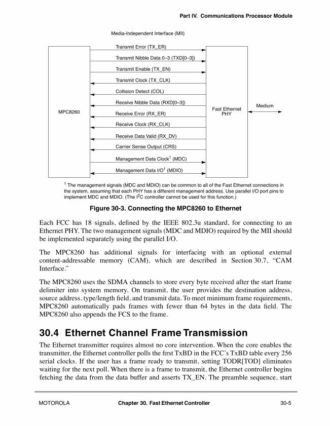
Part IV. Communications Processor Module
Figure 30-3. Connecting the MPC8260 to Ethernet
Each FCC has 18 signals, deÞned by the IEEE 802.3u standard, for connecting to anEthernet PHY. The two management signals (MDC and MDIO) required by the MII shouldbe implemented separately using the parallel I/O.
The MPC8260 has additional signals for interfacing with an optional externalcontent-addressable memory (CAM), which are described in Section 30.7, ÒCAMInterface.Ó
The MPC8260 uses the SDMA channels to store every byte received after the start framedelimiter into system memory. On transmit, the user provides the destination address,source address, type/length Þeld, and transmit data. To meet minimum frame requirements,MPC8260 automatically pads frames with fewer than 64 bytes in the data Þeld. TheMPC8260 also appends the FCS to the frame.
30.4 Ethernet Channel Frame TransmissionThe Ethernet transmitter requires almost no core intervention. When the core enables thetransmitter, the Ethernet controller polls the Þrst TxBD in the FCCÕs TxBD table every 256serial clocks. If the user has a frame ready to transmit, setting TODR[TOD] eliminateswaiting for the next poll. When there is a frame to transmit, the Ethernet controller beginsfetching the data from the data buffer and asserts TX_EN. The preamble sequence, start
Transmit Error (TX_ER)
Transmit Nibble Data 0Ð3 (TXD[0Ð3])
Transmit Enable (TX_EN)
Transmit Clock (TX_CLK)
Collision Detect (COL)
Receive Nibble Data (RXD[0Ð3])
Receive Error (RX_ER)
Receive Clock (RX_CLK)
Receive Data Valid (RX_DV)
Carrier Sense Output (CRS)
Management Data I/O1 (MDIO)
Management Data Clock1 (MDC)
MPC8260Fast Ethernet
PHY
Medium
Media-Independent Interface (MII)
1 The management signals (MDC and MDIO) can be common to all of the Fast Ethernet connections inthe system, assuming that each PHY has a different management address. Use parallel I/O port pins toimplement MDC and MDIO. (The I2C controller cannot be used for this function.)
MOTOROLA Chapter 30. Fast Ethernet Controller 30-5
Part IV. Communications Processor Module
frame delimiter, and frame information are sent in that order; see Figure 30-1. In full-duplex mode, since collisions are ignored, frame transmission maintains only theinterframe gap (96 serial clocks) regardless of CRS.
There is one internal buffer for out-of-sequence ßow control frames (in full-duplex FastEthernet). When the Fast Ethernet controller is between frames, this buffer is polled if ßowcontrol is enabled. This buffer must contain the whole frame.
However, in half-duplex mode, the controller defers transmission if the line is busy (CRSasserted). Before transmitting, the controller waits for carrier sense to become inactive, atwhich point the controller determines if CRS remains negated for 60 serial clocks. If so, thetransmission begins after an additional 36 serial clocks (96 serial clocks after CRSoriginally became negated).
If a collision occurs during the transmit frame, the Ethernet controller follows a speciÞedbackoff procedure and tries to retransmit the frame until the retry limit is reached. TheEthernet controller stores at least the Þrst 64 bytes of data of the transmit frame in the dual-port RAM, so that the data does not have to be retrieved from system memory in case of acollision. This improves bus usage and latency if the backoff timer output requires animmediate retransmission.
When the end of the current buffer is reached and TxBD[L] = 1, the FCS (32-bit CRC) bytesare appended (if TxBD[TC] = 1), and TX_EN is negated. This notiÞes the PHY of the needto generate the illegal Manchester encoding that signiÞes the end of an Ethernet frame.Following the transmission of the FCS, the Ethernet controller writes the frame status bitsinto the BD and clears TxBD[R]. When the end of the current buffer is reached andTxBD[L] = 0 (a frame is comprised of multiple buffers), only TxBD[R] is cleared.
For both half- and full-duplex modes, an interrupt can be issued depending on TxBD[I].The Ethernet controller then proceeds to the next TxBD in the table. In this way, the corecan be interrupted after each frame, after each buffer, or after a speciÞc buffer is sent. IfTxBD[PAD] = 1, the Ethernet controller pads short frames to the value of the minimumframe length register (MINFLR), described in Table 30-2.
To rearrange the transmit queue before the CP Þnishes sending all frames, issue aGRACEFUL STOP TRANSMIT command. This can be useful for transmitting expedited dataahead of previously linked buffers or for error situations. When the GRACEFUL STOP
TRANSMIT command is issued, the Ethernet controller stops immediately if no transmissionis in progress or continues transmission until the current frame either Þnishes or terminateswith a collision. When the Ethernet controller is given the RESTART TRANSMIT command,it resumes transmission. The Ethernet controller sends bytes least-signiÞcant nibble Þrst.
30-6 MPC8260 PowerQUICC II UserÕs Manual MOTOROLA
Part IV. Communications Processor Module
30.5 Ethernet Channel Frame ReceptionThe Ethernet receiver is designed to work with almost no core intervention and can performaddress recognition, CRC checking, short frame checking, maximum DMA transferchecking, and maximum frame-length checking.
When the core enables the Ethernet receiver, it enters hunt mode when RX_DV is assertedas long as COL remains negated (full-duplex mode ignores COL). In hunt mode, as data isshifted into the receive shift register four bits at a time, the contents of the register arecompared to the contents of the SYN2 Þeld in the FCCÕs data synchronization register(FDSR). When the registers match, the hunt mode is terminated and character assemblybegins.
When the receiver detects the Þrst bytes of a frame, the Ethernet controller performsaddress recognition functions on the frame; see Section 30.12, ÒEthernet AddressRecognition.Ó The receiver can receive physical (individual), group (multicast), andbroadcast addresses. Because Ethernet receive frame data is not written to memory until theinternal address recognition algorithm is complete, bus usage is not wasted on frames notaddressed to this station. The receiver can also operate with an external CAM, in which caseframe reception continues normally, unless the CAM speciÞcally signals the frame to berejected. See Section 30.7, ÒCAM Interface.Ó
If an address is recognized, the Ethernet controller fetches the next RxBD and, if it is empty,starts transferring the incoming frame to the RxBDÕs associated data buffer.
In half-duplex mode, if a collision is detected during the frame, the RxBDs associated withthis frame are reused. Thus, no collision frames are presented to the user except latecollisions, which indicate serious LAN problems. When the buffer has been Þlled, theEthernet controller clears RxBD[E] and generates an interrupt if RxBD[I] is set. If theincoming frame is larger than the buffer, the Ethernet controller fetches the next RxBD inthe table; if it is empty, it continues receiving the rest of the frame.
The RxBD length is determined by MRBLR in the parameter RAM. The user shouldprogram MRBLR to be at least 64 bytes. During reception, the Ethernet controller checksfor frames that are too short or too long. When the frame ends (CRS is negated), the receiveCRC Þeld is checked and written to the data buffer. The data length written to the last BDin the Ethernet frame is the length of the entire frame, which enables the software torecognize a frame-too-long condition.
If an external CAM is used (FPSMRx[CAM] = 1), the Ethernet controller adds the twolower bytes of the CAM output at the end of each frame. Note that the data length does notinclude these two bytes; that is, the extra two bytes could push the buffer length pastMRBLR.
When the receive frame is complete, the Ethernet controller sets RxBD[L], writes the otherframe status bits into the RxBD, and clears RxBD[E]. The Ethernet controller nextgenerates a maskable interrupt, indicating that a frame was received and is in memory. The
MOTOROLA Chapter 30. Fast Ethernet Controller 30-7
Part IV. Communications Processor Module
Ethernet controller then waits for a new frame. The Ethernet controller receives serial dataleast-signiÞcant nibble Þrst.
30.6 Flow ControlBecause collisions cannot occur in full-duplex mode, Fast Ethernet can operate at themaximum rate. When the rate becomes too fast for a stationÕs receiver, the stationÕstransmitter can send ßow-control frames to reduce the rate. Flow-control instructions aretransferred by special frames of minimum frame size. The length/type Þelds of these frameshave a special value. Table 30-1 shows the ßow-control frame structure.
When ßow-control mode is enabled (FPSMRx[FCE]) and the receiver identiÞes a pause-ßow control frame sent to individual or broadcast addresses, transmission stops for the timespeciÞed in the control frame. During this pause, only the out-of-sequence frame is sent.Normal transmission resumes after the pause timer stops counting. If another pause-controlframe is received during the pause, the period changes to the new value received.
30.7 CAM InterfaceThe MPC8260 internal address recognition logic can be used in combination with anexternal CAM. When using a CAM, the FCC must be in promiscuous mode(FPSMRx[PRO] = 1). See Section 30.12, ÒEthernet Address Recognition.Ó
The Ethernet controller writes two 32-bit accesses to the CAM and then reads the result ina 32-bit access. If the high bit of the result is set, the frame is rejected; otherwise, the lower16 bits are attached to the end of the frame.
Table 30-1. Flow Control Frame Structure
Size [Octets] Description Value Comment
7 Preamble
1 SFD Start frame delimiter
6 Destination address 01-80C2-00-00-01 Multicast address reserved for use in MAC frames
6 Source address
2 Length/type 88-08 Control frame type
2 MAC opcode 00-01 Pause command
2 MAC parameter Pause period measured in slot times, most-signiÞcant octet Þrst
42 Reserved Ñ
4 FCS Frame check sequence (CRC)
30-8 MPC8260 PowerQUICC II UserÕs Manual MOTOROLA
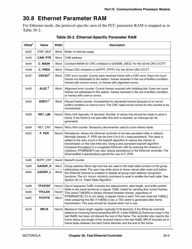
Part IV. Communications Processor Module
30.8 Ethernet Parameter RAMFor Ethernet mode, the protocol-speciÞc area of the FCC parameter RAM is mapped as inTable 30-2.
Table 30-2. Ethernet-Specific Parameter RAM
Offset1 Name Width Description
0x3C STAT_BUF Word Buffer of internal usage
0x40 CAM_PTR Word CAM address
0x44 C_MASK Word Constant MASK for CRC (initialize to 0xDEBB_20E3). For the 32-bit CRC-CCITT.
0x48 C_PRES Word Preset CRC (initialize to 0xFFFF_FFFF). For the 32-bit CRC-CCITT.
0x4C CRCEC2 Word CRC error counter. Counts each received frame with a CRC error. Does not count frames not addressed to the station, frames received in the out-of-buffers condition, frames with overrun errors, or frames with alignment errors.
0x50 ALEC 2 Word Alignment error counter. Counts frames received with dribbling bits. Does not count frames not addressed to the station, frames received in the out-of-buffers condition, or frames with overrun errors.
0x54 DISFC 2 Word Discard frame counter. Incremented for discarded frames because of an out-of-buffers condition or overrun error. The CRC need not be correct for this counter to be incremented.
0x58 RET_LIM Hword Retry limit (typically 15 decimal). Number of retries that should be made to send a frame. If the frame is not sent after this limit is reached, an interrupt can be generated.
0x5A RET_CNT Hword Retry limit counter. Temporary decrementer used to count retries made.
0x5C P_PER Hword Persistence. Allows the Ethernet controller to be less persistent after a collision. Normally cleared, P_PER can be from 0 to 9 (9 = least persistent). The value is added to the retry count in the backoff algorithm to reduce the chance of transmission on the next time-slot. Using a less persistent backoff algorithm increases throughput in a congested Ethernet LAN by reducing the chance of collisions. FPSMR[SBT] can also reduce persistence of the Ethernet controller. The Ethernet/802.3 speciÞcations permit the use of P_PER.
0x5E BOFF_CNT Hword Backoff counter
0x60 GADDR_H Word Group address Þlters high and low are used in the hash table function of the group addressing mode. The user may write zeros to these values after reset and before the Ethernet channel is enabled to disable all group hash address recognition functions. The SET GROUP ADDRESS command is used to enable the hash table. See Section 30.13, ÒHash Table Algorithm.Ó
0x64 GADDR_L Word
0x68 TFCSTAT Hword Out-of-sequence TxBD. Includes the status/control, data length, and buffer pointer Þelds in the same format as a regular TxBD. Useful for sending ßow control frames. This areaÕs TxBD[R] is always checked between frames, regardless of FPSMRx[FCE]. If it is not ready, a regular frame is sent. The user must set TxBD[L] when preparing this BD. If TxBD[I] is set, a TXC event is generated after frame transmission. This area should be cleared when not in use.
0x6A TFCLEN Hword
0x6C TFCPTR Word
0x70 MFLR Hword Maximum frame length register (typically1518 decimal). If the Ethernet controller detects an incoming frame exceeding MFLR, it sets RxBD[LG] (frame too long) in the last RxBD, but does not discard the rest of the frame. The controller also reports the frame status and length of the received frame in the last RxBD. MFLR includes all in-frame bytes between the start frame delimiter and the end of the frame.
MOTOROLA Chapter 30. Fast Ethernet Controller 30-9
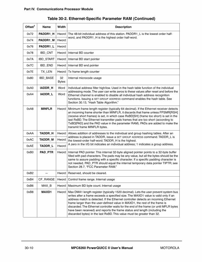
Part IV. Communications Processor Module
0x72 PADDR1_H Hword The 48-bit individual address of this station. PADDR1_L is the lowest order half-word, and PADDR1_H is the highest order half-word.
0x74 PADDR1_M Hword
0x76 PADDR1_L Hword
0x78 IBD_CNT Hword Internal BD counter
0x7A IBD_START Hword Internal BD start pointer
0x7C IBD_END Hword Internal BD end pointer
0x7E TX_LEN Hword Tx frame length counter
0x80 IBD_BASE 32 Bytes
Internal microcode usage
0xA0 IADDR_H Word Individual address Þlter high/low. Used in the hash table function of the individual addressing mode. The user can write zeros to these values after reset and before the Ethernet channel is enabled to disable all individual hash address recognition functions. Issuing a SET GROUP ADDRESS command enables the hash table. See Section 30.13, ÒHash Table Algorithm.Ó
0xA4 IADDR_L Word
0xA8 MINFLR Hword Minimum frame length register (typically 64 decimal). If the Ethernet receiver detects an incoming frame shorter than MINFLR, it discards that frame unless FPSMR[RSH] (receive short frames) is set, in which case RxBD[SH] (frame too short) is set in the last RxBD. The Ethernet transmitter pads frames that are too short (according to TxBD[PAD] and the PAD value in the parameter RAM). PADs are added to make the transmit frame MINFLR bytes.
0xAA TADDR_H Hword Allows addition of addresses to the individual and group hashing tables. After an address is placed in TADDR, issue a SET GROUP ADDRESS command. TADDR_L is the lowest-order half-word; TADDR_H is the highest. A zero in the I/G bit indicates an individual address; 1 indicates a group address.
0xAC TADDR_M Hword
0xAE TADDR_L Hword
0xB0 PAD_PTR Hword Internal PAD pointer. This internal 32-byte aligned pointer points to a 32-byte buffer Þlled with pad characters. The pads may be any value, but all the bytes should be the same to assure padding with a speciÞc character. If a speciÞc padding character is not needed, PAD_PTR should equal the internal temporary data pointer TIPTR; see Section 28.7, ÒFCC Parameter RAM.Ó
0xB2 Ñ Hword Reserved, should be cleared.
0xB4 CF_RANGE Hword Control frame range. Internal usage
0xB6 MAX_B Hword Maximum BD byte count. Internal usage
0xB8 MAXD1 Hword Max DMA1 length register (typically 1520 decimal). Lets the user prevent system bus writes after a frame exceeds a speciÞed size. The MAXD1 value is valid only if an address match is detected. If the Ethernet controller detects an incoming Ethernet frame larger than the user-deÞned value in MAXD1, the rest of the frame is discarded. The Ethernet controller waits for the end of the frame (or until MFLR bytes have been received) and reports the frame status and length (including the discarded bytes) in the last RxBD. This value must be greater than 32.
Table 30-2. Ethernet-Specific Parameter RAM (Continued)
Offset1 Name Width Description
30-10 MPC8260 PowerQUICC II UserÕs Manual MOTOROLA
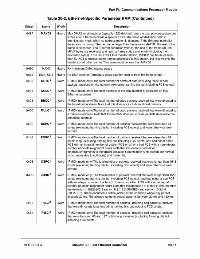
Part IV. Communications Processor Module
0xBA MAXD2 Hword Max DMA2 length register (typically 1520 decimal). Lets the user prevent system bus writes after a frame exceeds a speciÞed size. The value of MAXD2 is valid in promiscuous mode when no address match is detected. If the Ethernet controller detects an incoming Ethernet frame larger than the value in MAXD2, the rest of the frame is discarded. The Ethernet controller waits for the end of the frame (or until MFLR bytes are received) and reports frame status and length (including the discarded bytes) in the last RxBD. In a monitor station, MAXD2 can be much less than MAXD1 to receive entire frames addressed to this station, but receive only the headers of all other frames.This value must be less than MAXD1.
0xBC MAXD Hword Rx maximum DMA. Internal usage
0xBE DMA_CNT Hword Rx DMA counter. Temporary down-counter used to track the frame length.
0xC0 OCTC 2 Word (RMON mode only) The total number of octets of data (including those in bad packets) received on the network (excluding framing bits but including FCS octets).
0xC4 COLC 2 Word (RMON mode only) The best estimate of the total number of collisions on this Ethernet segment.
0xC8 BROC 2 Word (RMON mode only) The total number of good packets received that were directed to the broadcast address. Note that this does not include multicast packets.
0xCC MULC 2 Word (RMON mode only) The total number of good packets received that were directed to a multicast address. Note that this number does not include packets directed to the broadcast address.
0xD0 USPC 2 Word (RMON mode only) The total number of packets received that were less than 64 octets (excluding framing bits but including FCS octets) and were otherwise well-formed.
0xD4 FRGC 2 Word (RMON mode only) The total number of packets received that were less than 64 octets long (excluding framing bits but including FCS octets) and had either a bad FCS with an integral number of octets (FCS error) or a bad FCS with a non-integral number of octets (alignment error). Note that it is entirely normal for etherStatsFragments to increment because it counts both runts (which are normal occurrences due to collisions) and noise hits.
0xD8 OSPC 2 Word (RMON mode only) The total number of packets received that were longer than 1518 octets (excluding framing bits but including FCS octets) and were otherwise well-formed.
0xDC JBRC 2 Word (RMON mode only) The total number of packets received that were longer than 1518 octets (excluding framing bits but including FCS octets), and had either a bad FCS with an integral number of octets (FCS error) or a bad FCS with a non-integral number of octets (alignment error). Note that this deÞnition of jabber is different than the deÞnition in IEEE-802.3 section 8.2.1.5 (10BASE5) and section 10.3.1.4 (10BASE2). These documents deÞne jabber as the condition where any packet exceeds 20 ms. The allowed range to detect jabber is between 20 ms and 150 ms.
0xE0 P64C 2 Word (RMON mode only) The total number of packets (including bad packets) received that were 64 octets long (excluding framing bits but including FCS octets).
0xE4 P65C 2 Word (RMON mode only) The total number of packets (including bad packets) received that were between 65 and 127 octets long inclusive (excluding framing bits but including FCS octets).
Table 30-2. Ethernet-Specific Parameter RAM (Continued)
Offset1 Name Width Description
MOTOROLA Chapter 30. Fast Ethernet Controller 30-11
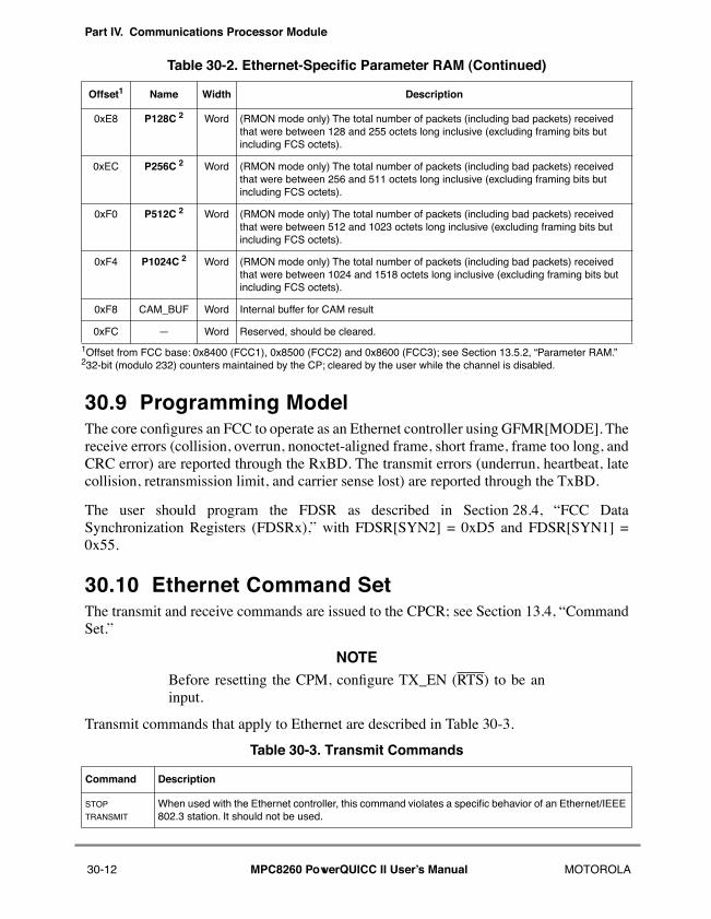
Part IV. Communications Processor Module
30.9 Programming ModelThe core conÞgures an FCC to operate as an Ethernet controller using GFMR[MODE]. Thereceive errors (collision, overrun, nonoctet-aligned frame, short frame, frame too long, andCRC error) are reported through the RxBD. The transmit errors (underrun, heartbeat, latecollision, retransmission limit, and carrier sense lost) are reported through the TxBD.
The user should program the FDSR as described in Section 28.4, ÒFCC DataSynchronization Registers (FDSRx),Ó with FDSR[SYN2] = 0xD5 and FDSR[SYN1] =0x55.
30.10 Ethernet Command SetThe transmit and receive commands are issued to the CPCR; see Section 13.4, ÒCommandSet.Ó
NOTEBefore resetting the CPM, conÞgure TX_EN (RTS) to be aninput.
Transmit commands that apply to Ethernet are described in Table 30-3.
0xE8 P128C 2 Word (RMON mode only) The total number of packets (including bad packets) received that were between 128 and 255 octets long inclusive (excluding framing bits but including FCS octets).
0xEC P256C 2 Word (RMON mode only) The total number of packets (including bad packets) received that were between 256 and 511 octets long inclusive (excluding framing bits but including FCS octets).
0xF0 P512C 2 Word (RMON mode only) The total number of packets (including bad packets) received that were between 512 and 1023 octets long inclusive (excluding framing bits but including FCS octets).
0xF4 P1024C 2 Word (RMON mode only) The total number of packets (including bad packets) received that were between 1024 and 1518 octets long inclusive (excluding framing bits but including FCS octets).
0xF8 CAM_BUF Word Internal buffer for CAM result
0xFC Ñ Word Reserved, should be cleared.
1Offset from FCC base: 0x8400 (FCC1), 0x8500 (FCC2) and 0x8600 (FCC3); see Section 13.5.2, ÒParameter RAM.Ó232-bit (modulo 232) counters maintained by the CP; cleared by the user while the channel is disabled.
Table 30-3. Transmit Commands
Command Description
STOP TRANSMIT
When used with the Ethernet controller, this command violates a speciÞc behavior of an Ethernet/IEEE 802.3 station. It should not be used.
Table 30-2. Ethernet-Specific Parameter RAM (Continued)
Offset1 Name Width Description
30-12 MPC8260 PowerQUICC II UserÕs Manual MOTOROLA
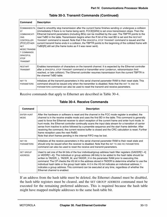
Part IV. Communications Processor Module
Receive commands that apply to Ethernet are described in Table 30-4.
If an address from the hash table must be deleted, the Ethernet channel must be disabled,the hash table registers must be cleared, and the SET GROUP ADDRESS command must beexecuted for the remaining preferred addresses. This is required because the hash tablemight have mapped multiple addresses to the same hash table bit.
COMMANDS:FA
ST COMMUNICATI
ONS CONTROLLER (FCC):ETHER
NET MODE:TRANSMI
T COMMANDS GRACEFUL STOP TRANSMIT
Used to smoothly stop transmission after the current frame Þnishes sending or undergoes a collision (immediately if there is no frame being sent). FCCE[GRA] is set once transmission stops. Then the Ethernet transmit parameters (including BDs) can be modiÞed by the user. The TBPTR points to the next TxBD in the table. Transmission begins when the R bit of the next BD is set and the RESTART TRANSMIT command is issued. Note that if the GRACEFUL STOP TRANSMIT command is issued and the current transmit frame ends in a collision, the TBPTR points to the beginning of the collided frame with TxBD[R] still set (the frame looks as if it was never sent).
RESTART TRANSMIT
Enables transmission of characters on the transmit channel. It is expected by the Ethernet controller after a GRACEFUL STOP TRANSMIT command or transmitter error (underrun, retransmission limit reached, or late collision). The Ethernet controller resumes transmission from the current TBPTR in the channel TxBD table.
INIT TX PARAMETERS
Initializes all the transmit parameters in this serial channel parameter RAM to their reset state. This command should be issued only when the transmitter is disabled. Note that the INIT TX AND RX PARAMETERS command can also be used to reset the transmit and receive parameters.
Table 30-4. Receive Commands
Command Description
ENTER HUNT MODE
After the hardware or software is reset and the channel in the FCC mode register is enabled, the channel is in the receive enable mode and uses the Þrst BD in the table. This command is generally used to force the Ethernet receiver to abort reception of the current frame and enter hunt mode. In hunt mode, the Ethernet controller continually scans the input data stream for a transition of carrier sense from inactive to active followed by a preamble sequence and the start frame delimiter. After receiving the command, the current receive buffer is closed and the CRC calculation is reset. Further frame reception uses the next RxBD. Note that short frames pending in the internal FIFO may be lost.
INIT RX PARAMETERS
Initializes all the receive parameters in this serial channel parameter RAM to their reset state and should only be issued when the receiver is disabled. Note that the INIT TX AND RX PARAMETERS command can also be used to reset the receive and transmit parameters.
SET GROUP ADDRESS
Used to set one of the 64 bits of the four individual/group address hash Þlter registers (GADDR[1Ð4] or IADDR[1Ð4]). The individual or group address (48 bits) to be added to the hash table should be written to TADDR_L, TADDR_M, and TADDR_H in the parameter RAM prior to executing this command. The CP checks the I/G bit in the address stored in TADDR to determine whether to use the individual hash table or the group hash table. A 0 in the I/G bit indicates an individual address; 1 indicates a group address. This command can be executed at any time, regardless of whether the Ethernet channel is enabled.
Table 30-3. Transmit Commands (Continued)
Command Description
MOTOROLA Chapter 30. Fast Ethernet Controller 30-13
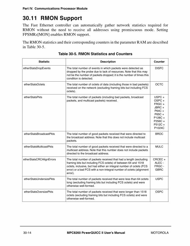
Part IV. Communications Processor Module
30.11 RMON SupportThe Fast Ethernet controller can automatically gather network statistics required forRMON without the need to receive all addresses using promiscuous mode. SettingFPSMRx[MON] enables RMON support.
The RMON statistics and their corresponding counters in the parameter RAM are describedin Table 30-5.
Table 30-5. RMON Statistics and Counters
Statistic Description Counter
etherStatsDropEvents The total number of events in which packets were detected as dropped by the probe due to lack of resources. Note that this may not be the number of packets dropped; it is the number of times this condition is detected.
DISFC
etherStatsOctets The total number of octets of data (including those in bad packets) received on the network (excluding framing bits but including FCS octets).
OCTC
etherStatsPkts The total number of packets (including bad packets, broadcast packets, and multicast packets) received.
USPC + OSPC + FRGC + JBRC + P64C + P65C + P128C + P256C + P512C + P1024C
etherStatsBroadcastPkts The total number of good packets received that were directed to the broadcast address. Note that this does not include multicast packets.
BROC
etherStatsMulticastPkts The total number of good packets received that were directed to a multicast address. Note that this number does not include packets directed to the broadcast address.
MULC
etherStatsCRCAlignErrors The total number of packets received that had a length (excluding framing bits but including FCS octets) of between 64 and 1518 octets, inclusive, but had either an integral number of octets (FCS error) or a bad FCS with a non-integral number of octets (alignment error).
CRCEC + ALEC -FRGC -GBRC
etherStatsUndersizePkts The total number of packets received that were less than 64 octets long (excluding framing bits but including FCS octets) and were otherwise well-formed.
USPC
etherStatsOversizePkts The total number of packets received that were longer than 1518 octets (excluding framing bits but including FCS octets) and were otherwise well-formed.
OSPC
30-14 MPC8260 PowerQUICC II UserÕs Manual MOTOROLA
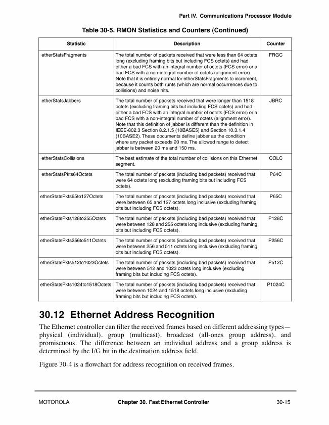
Part IV. Communications Processor Module
30.12 Ethernet Address RecognitionThe Ethernet controller can Þlter the received frames based on different addressing typesÑphysical (individual), group (multicast), broadcast (all-ones group address), andpromiscuous. The difference between an individual address and a group address isdetermined by the I/G bit in the destination address Þeld.
Figure 30-4 is a ßowchart for address recognition on received frames.
etherStatsFragments The total number of packets received that were less than 64 octets long (excluding framing bits but including FCS octets) and had either a bad FCS with an integral number of octets (FCS error) or a bad FCS with a non-integral number of octets (alignment error). Note that it is entirely normal for etherStatsFragments to increment, because it counts both runts (which are normal occurrences due to collisions) and noise hits.
FRGC
etherStatsJabbers The total number of packets received that were longer than 1518 octets (excluding framing bits but including FCS octets) and had either a bad FCS with an integral number of octets (FCS error) or a bad FCS with a non-integral number of octets (alignment error). Note that this deÞnition of jabber is different than the deÞnition in IEEE-802.3 Section 8.2.1.5 (10BASE5) and Section 10.3.1.4 (10BASE2). These documents deÞne jabber as the condition where any packet exceeds 20 ms. The allowed range to detect jabber is between 20 ms and 150 ms.
JBRC
etherStatsCollisions The best estimate of the total number of collisions on this Ethernet segment.
COLC
etherStatsPkts64Octets The total number of packets (including bad packets) received that were 64 octets long (excluding framing bits but including FCS octets).
P64C
etherStatsPkts65to127Octets The total number of packets (including bad packets) received that were between 65 and 127 octets long inclusive (excluding framing bits but including FCS octets).
P65C
etherStatsPkts128to255Octets The total number of packets (including bad packets) received that were between 128 and 255 octets long inclusive (excluding framing bits but including FCS octets).
P128C
etherStatsPkts256to511Octets The total number of packets (including bad packets) received that were between 256 and 511 octets long inclusive (excluding framing bits but including FCS octets).
P256C
etherStatsPkts512to1023Octets The total number of packets (including bad packets) received that were between 512 and 1023 octets long inclusive (excluding framing bits but including FCS octets).
P512C
etherStatsPkts1024to1518Octets The total number of packets (including bad packets) received that were between 1024 and 1518 octets long inclusive (excluding framing bits but including FCS octets).
P1024C
Table 30-5. RMON Statistics and Counters (Continued)
Statistic Description Counter
MOTOROLA Chapter 30. Fast Ethernet Controller 30-15
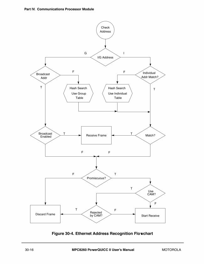
Part IV. Communications Processor Module
Figure 30-4. Ethernet Address Recognition Flowchart
CheckAddress
I/G Address
IndividualAddr Match?
IG
BroadcastAddr
BroadcastEnabled
T
Receive FrameT
Hash Search
Use GroupTable
Hash Search
Use IndividualTable
T
Match?T
Promiscuous?
Discard Frame
TF
FF
FF
UseCAM?
Start ReceiveRejectedby CAM?
FT
T
F
30-16 MPC8260 PowerQUICC II UserÕs Manual MOTOROLA
Part IV. Communications Processor Module
In the physical type of address recognition, the Ethernet controller compares the destinationaddress Þeld of the received frame with the physical address that the user programs in thePADDR. If it fails, the controller performs address recognition on multiple individualaddresses using the IADDR_H/L hash table. Since the controller always checks PADDRand the individual hash, for individual address the user must write zeros to the hash in orderto avoid a hash match and ones to PADDR in order to avoid individual address match.
In the group type of address recognition, the Ethernet controller determines whether thegroup address is a broadcast address. If it is a broadcast and broadcast addresses areenabled, the frame is accepted. If the group address is not a broadcast address, the user canperform address recognition on multiple group addresses using the GADDR_H/L hashtable. In promiscuous mode, the Ethernet controller receives all of the incoming framesregardless of their address when an external CAM is not used.
If an external CAM is used for address recognition (FPSMR[CAM] = 1), the user shouldselect promiscuous mode; the frame can be rejected if there is no match in the CAM. If theon-chip address recognition functions detect a match, the external CAM is not accessed.
30.13 Hash Table AlgorithmThe hash table process used in the individual and group hash Þltering operates as follows.The Ethernet controller maps any 48-bit address into one of 64 bins, which are representedby the 64 bits in GADDR_H/L or IADDR_H/L. When the SET GROUP ADDRESS commandis executed, the Ethernet controller maps the selected 48-bit address in TADDR into one ofthe 64 bits. This is performed by passing the 48-bit address through the on-chip 32-bit CRCgenerator and using 6 bits of the CRC-encoded result to generate a number between 1 and64. Bit 26 of the CRC result selects between the two GADDRs or IADDRs; bits 27Ð31 ofthe CRC result select which bit is set.
The same process is used when the Ethernet controller receives a frame. If the CRCgenerator selects a bit that is set in the group/individual hash table, the frame is accepted;otherwise, it is rejected. The result is that if eight group addresses are stored in the hashtable and random group addresses are received, the hash table prevents roughly 56/64(87.5%) of the group address frames from reaching memory. The core must further Þlterthose that reach memory to determine if they contain one of the eight preferred addresses.
Better performance is achieved by using the group and individual hash tables incombination. For instance, if eight group and eight physical addresses are stored in theirrespective hash tables, 87.5% of all frames (not just group address frames) are preventedfrom reaching memory.
The effectiveness of the hash table declines as the number of addresses increases. Forinstance, with 128 addresses stored in a 64-bin hash table, the vast majority of the hash tablebits are set, preventing only a small fraction of frames from reaching memory. In suchinstances, an external CAM is advised if the extra bus use cannot be tolerated. SeeSection 30.7, ÒCAM Interface.Ó
MOTOROLA Chapter 30. Fast Ethernet Controller 30-17
Part IV. Communications Processor Module
NOTEThe hash tables cannot be used to reject frames that match a setof selected addresses because unintended addresses can map tothe same bit in the hash table. Thus, an external CAM must beused to implement this function.
30.14 Interpacket Gap TimeThe minimum interpacket gap time for back-to-back transmission is 96 serial clocks. Thereceiver receives back-to-back frames with this minimum spacing. In addition, after thebackoff algorithm, the transmitter waits for carrier sense to be negated before retransmittingthe frame. The retransmission begins 96 serial clocks after carrier sense is negated if it staysnegated for at least 60 serial clocks. So if there is no change in the carrier sense indicationduring the Þrst 60 serial clocks after the retransmission begins 96 clocks after carrier senseis Þrst negated
30.15 Handling Collisions If a collision occurs during frame transmission, the Ethernet controller continuestransmission for at least 32-bit times, transmitting a jam pattern of 32 ones. If the collisionoccurs during the preamble sequence, the jam pattern is sent after the sequence ends.
If a collision occurs within 64 byte times, the process is retried. The transmitter waits arandom number of slot times. (A slot time is 512 bit times.) If a collision occurs after 64byte times, no retransmission is performed, FCCE[TXE] is set, and the buffer is closed witha late-collision error indication in TxBD[LC]. If a collision occurs during frame reception,reception is stopped. This error is reported only in the RxBD if the frame is at least as longas the MINFLR or if FPSMR[RSH] = 1.
30.16 Internal and External LoopbackBoth internal and external loopback are supported by the Ethernet controller. In loopbackmode, both receive and transmit FIFO buffers are used and the FCC operates in full-duplex.Both internal and external loopback are conÞgured using combinations of FPSMR[LPB]and GFMR[DIAG]. Because of the full-duplex nature of the loopback operation, theperformance of the other FCCs is degraded.
Internal loopback disconnects the FCC from the SI. The receive data is connected to thetransmit data. The transmitted data from the transmit FIFO is received immediately into thereceive FIFO. There is no heartbeat check in this mode.
In external loopback operation, the Ethernet controller listens for data received from thePHY while it is sending.
30-18 MPC8260 PowerQUICC II UserÕs Manual MOTOROLA
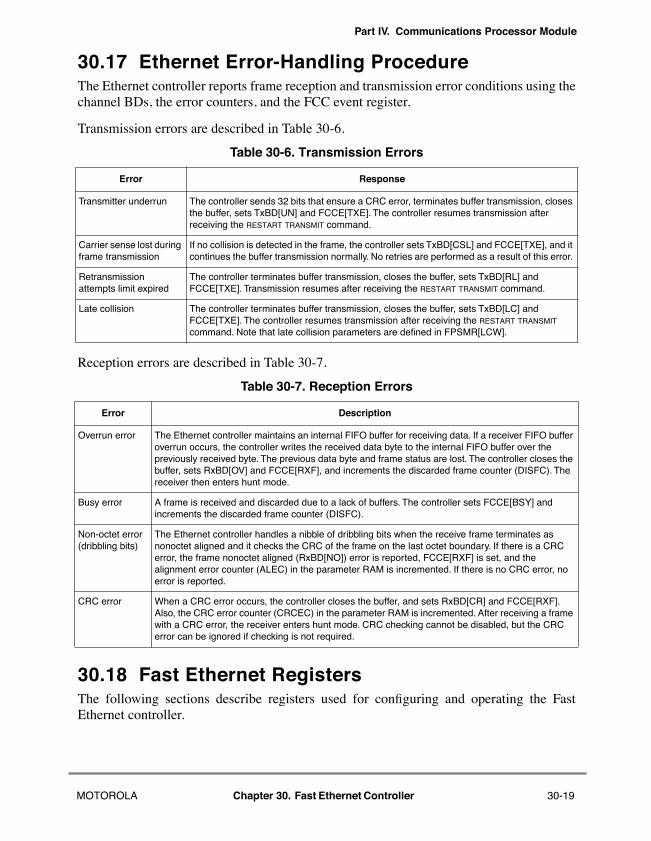
Part IV. Communications Processor Module
30.17 Ethernet Error-Handling ProcedureThe Ethernet controller reports frame reception and transmission error conditions using thechannel BDs, the error counters, and the FCC event register.
Transmission errors are described in Table 30-6.
Reception errors are described in Table 30-7.
30.18 Fast Ethernet RegistersThe following sections describe registers used for conÞguring and operating the FastEthernet controller.
Table 30-6. Transmission Errors
Error Response
Transmitter underrun The controller sends 32 bits that ensure a CRC error, terminates buffer transmission, closes the buffer, sets TxBD[UN] and FCCE[TXE]. The controller resumes transmission after receiving the RESTART TRANSMIT command.
Carrier sense lost during frame transmission
If no collision is detected in the frame, the controller sets TxBD[CSL] and FCCE[TXE], and it continues the buffer transmission normally. No retries are performed as a result of this error.
Retransmission attempts limit expired
The controller terminates buffer transmission, closes the buffer, sets TxBD[RL] and FCCE[TXE]. Transmission resumes after receiving the RESTART TRANSMIT command.
Late collision The controller terminates buffer transmission, closes the buffer, sets TxBD[LC] and FCCE[TXE]. The controller resumes transmission after receiving the RESTART TRANSMIT command. Note that late collision parameters are deÞned in FPSMR[LCW].
Table 30-7. Reception Errors
Error Description
Overrun error The Ethernet controller maintains an internal FIFO buffer for receiving data. If a receiver FIFO buffer overrun occurs, the controller writes the received data byte to the internal FIFO buffer over the previously received byte. The previous data byte and frame status are lost. The controller closes the buffer, sets RxBD[OV] and FCCE[RXF], and increments the discarded frame counter (DISFC). The receiver then enters hunt mode.
Busy error A frame is received and discarded due to a lack of buffers. The controller sets FCCE[BSY] and increments the discarded frame counter (DISFC).
Non-octet error (dribbling bits)
The Ethernet controller handles a nibble of dribbling bits when the receive frame terminates as nonoctet aligned and it checks the CRC of the frame on the last octet boundary. If there is a CRC error, the frame nonoctet aligned (RxBD[NO]) error is reported, FCCE[RXF] is set, and the alignment error counter (ALEC) in the parameter RAM is incremented. If there is no CRC error, no error is reported.
CRC error When a CRC error occurs, the controller closes the buffer, and sets RxBD[CR] and FCCE[RXF]. Also, the CRC error counter (CRCEC) in the parameter RAM is incremented. After receiving a frame with a CRC error, the receiver enters hunt mode. CRC checking cannot be disabled, but the CRC error can be ignored if checking is not required.
MOTOROLA Chapter 30. Fast Ethernet Controller 30-19

Part IV. Communications Processor Module
30.18.1 FCC Ethernet Mode Register (FPSMR)In Ethernet mode, the FCC protocol-speciÞc mode register, shown in Figure 30-5,functions as the Ethernet mode register.
Table 30-8 describes FPSMR Þelds.
Bits 0 1 2 3 4 5 6 7 8 9 10 11 12 13 14 15
Field HBC FC SBT LPB LCW FDE MON Ñ PRO FCE RSH Ñ
Reset 0000_0000_0000_0000
R/W R/W
Addr 0x11304 (FPSMR1), 0x11324 (FPSMR2), 0x11324 (FPSMR3)
Bits 16 17 18 19 20 21 22 23 24 25 26 27 28 29 30 31
Field Ñ CAM BRO Ñ CRC Ñ
Reset 0000_0000_0000_0000
R/W R/W
Addr 0x11306 (FPSMR1), 0x11326 (FPSMR2), 0x11326 (FPSMR3)
Figure 30-5. FCC Ethernet Mode Registers (FPSMR)
Table 30-8. FPSMR Ethernet Field Descriptions
Bits Name Description
0 HBC Heartbeat checking0 Heartbeat checking is not performed. Do not wait for a collision after transmission.1 Wait 40 transmit serial clocks for a collision asserted by the transceiver after transmission.
TxBD[HB] is set if the heartbeat is not heard within 40 transmit serial clocks.
1 FC Force collision0 Normal operation.1 The controller forces a collision on transmission of every transmit frame. The MPC8260
should be conÞgured in loopback operation when using this feature, which allows the user to test the MPC8260 collision logic. It causes the retry limit to be exceeded for each transmit frame.
2 SBT Stop backoff timer 0 The backoff timer functions normally.1 The backoff timer (for the random wait after a collision) is stopped whenever carrier sense is
active. In this method, the retransmission is less aggressive than the maximum allowed in the IEEE 802.3 standard. The persistence (P_PER) feature in the parameter RAM can be used in combination with the SBT bit (or in place of the SBT bit).
3 LPB Local protect bit0 Receiver is blocked when transmitter sends (default).1 Receiver is not blocked when transmitter sends. Must be set for full-duplex operation. For
loopback operation, GFMR[DIAG] must be programmed also; see Section 28.2, ÒGeneral FCC Mode Registers (GFMRx).Ó
4 LCW Late collision window0 A late collision is any collision that occurs at least 64 bytes from the preamble.1 A late collision is any collision that occurs at least 56 bytes from the preamble.
30-20 MPC8260 PowerQUICC II UserÕs Manual MOTOROLA
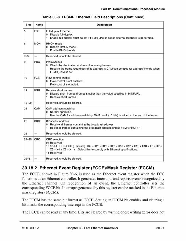
Part IV. Communications Processor Module
30.18.2 Ethernet Event Register (FCCE)/Mask Register (FCCM)The FCCE, shown in Figure 30-6, is used as the Ethernet event register when the FCCfunctions as an Ethernet controller. It generates interrupts and reports events recognized bythe Ethernet channel. On recognition of an event, the Ethernet controller sets thecorresponding FCCE bit. Interrupts generated by this register can be masked in the Ethernetmask register (FCCM).
The FCCM has the same bit format as FCCE. Setting an FCCM bit enables and clearing abit masks the corresponding interrupt in the FCCE.
The FCCE can be read at any time. Bits are cleared by writing ones; writing zeros does not
5 FDE Full duplex Ethernet 0 Disable full-duplex.1 Enable full-duplex. Must be set if FSMR[LPB] is set or external loopback is performed.
6 MON RMON mode0 Disable RMON mode.1 Enable RMON mode.
7Ð8 Ñ Reserved, should be cleared.
9 PRO Promiscuous 0 Check the destination address of incoming frames.1 Receive the frame regardless of its address. A CAM can be used for address Þltering when
FSMR[CAM] is set.
10 FCE Flow control enable0 Flow control is not enabled.1 Flow control is enabled.
11 RSH Receive short frames0 Discard short frames (frames smaller than the value speciÞed in MINFLR).1 Receive short frames.
12Ð20 Ñ Reserved, should be cleared.
21 CAM CAM address matching0 Normal operation.1 Use the CAM for address matching; CAM result (16 bits) is added at the end of the frame.
22 BRO Broadcast address 0 Receive all frames containing the broadcast address.1 Reject all frames containing the broadcast address unless FSMR[PRO] = 1.
23 Ñ Reserved, should be cleared.
24Ð25 CRC CRC selection 0x Reserved.10 32-bit CCITT-CRC (Ethernet). X32 + X26 + X23 + X22 + X16 + X12 + X11 + X10 + X8 + X7 +
X5 + X4 + X2 + X1 +1. Select this to comply with Ethernet speciÞcations.11 Reserved.
26Ð31 Ñ Reserved, should be cleared.
Table 30-8. FPSMR Ethernet Field Descriptions (Continued)
Bits Name Description
MOTOROLA Chapter 30. Fast Ethernet Controller 30-21
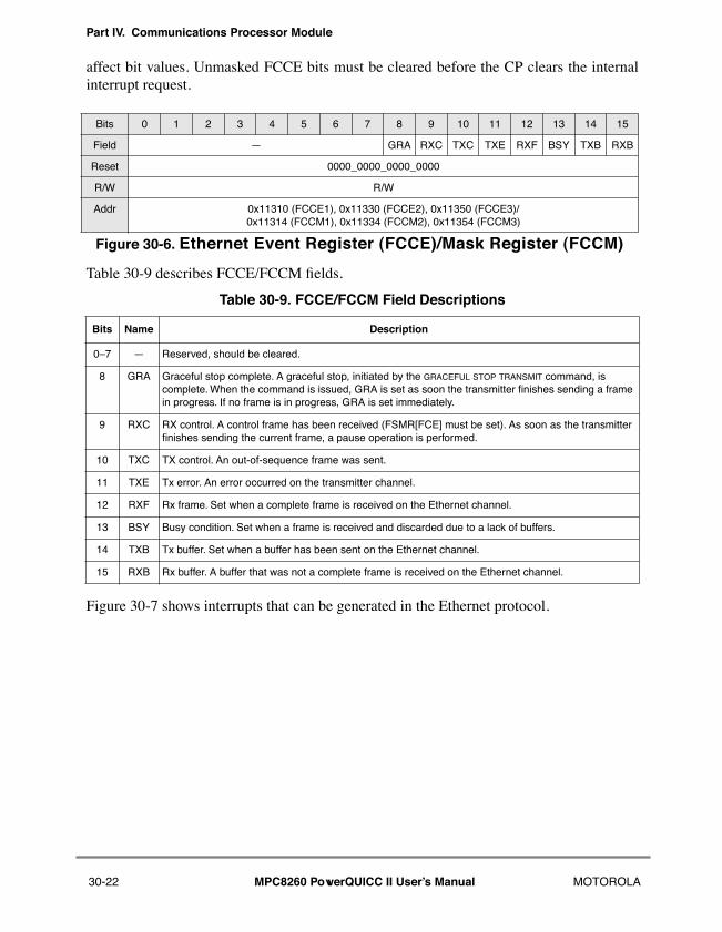
Part IV. Communications Processor Module
affect bit values. Unmasked FCCE bits must be cleared before the CP clears the internalinterrupt request.
Table 30-9 describes FCCE/FCCM Þelds.
Figure 30-7 shows interrupts that can be generated in the Ethernet protocol.
Bits 0 1 2 3 4 5 6 7 8 9 10 11 12 13 14 15
Field Ñ GRA RXC TXC TXE RXF BSY TXB RXB
Reset 0000_0000_0000_0000
R/W R/W
Addr 0x11310 (FCCE1), 0x11330 (FCCE2), 0x11350 (FCCE3)/0x11314 (FCCM1), 0x11334 (FCCM2), 0x11354 (FCCM3)
Figure 30-6. Ethernet Event Register (FCCE)/Mask Register (FCCM)
Table 30-9. FCCE/FCCM Field Descriptions
Bits Name Description
0Ð7 Ñ Reserved, should be cleared.
8 GRA Graceful stop complete. A graceful stop, initiated by the GRACEFUL STOP TRANSMIT command, is complete. When the command is issued, GRA is set as soon the transmitter Þnishes sending a frame in progress. If no frame is in progress, GRA is set immediately.
9 RXC RX control. A control frame has been received (FSMR[FCE] must be set). As soon as the transmitter Þnishes sending the current frame, a pause operation is performed.
10 TXC TX control. An out-of-sequence frame was sent.
11 TXE Tx error. An error occurred on the transmitter channel.
12 RXF Rx frame. Set when a complete frame is received on the Ethernet channel.
13 BSY Busy condition. Set when a frame is received and discarded due to a lack of buffers.
14 TXB Tx buffer. Set when a buffer has been sent on the Ethernet channel.
15 RXB Rx buffer. A buffer that was not a complete frame is received on the Ethernet channel.
30-22 MPC8260 PowerQUICC II UserÕs Manual MOTOROLA
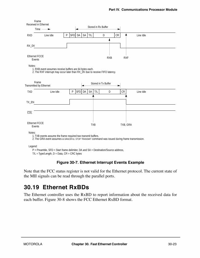
Part IV. Communications Processor Module
Figure 30-7. Ethernet Interrupt Events Example
Note that the FCC status register is not valid for the Ethernet protocol. The current state ofthe MII signals can be read through the parallel ports.
30.19 Ethernet RxBDsThe Ethernet controller uses the RxBD to report information about the received data foreach buffer. Figure 30-8 shows the FCC Ethernet RxBD format.
RXB
Line Idle
Stored in Rx Buffer
RXD
RX_DV
FrameReceived in Ethernet
Time
Line Idle
TXD
TX_EN
FrameTransmitted by Ethernet
COL
TXB, GRATXB
Line Idle Line Idle
Stored in Tx Buffer
Notes:
Ethernet FCCEEvents
1. RXB event assumes receive buffers are 64 bytes each.2. The RXF interrupt may occur later than RX_DV due to receive FIFO latency.
Notes:
Ethernet FCCEEvents
1. TXB events assume the frame required two transmit buffers.2. The GRA event assumes a GRACEFUL STOP TRANSMIT command was issued during frame transmission.
P SFD DA SA CR
RXF
T/L D
P SFD DA SA CRT/L D
Legend:P = Preamble, SFD = Start frame delimiter, DA and SA = Destination/Source address,T/L = Type/Length, D = Data, CR = CRC bytes
MOTOROLA Chapter 30. Fast Ethernet Controller 30-23
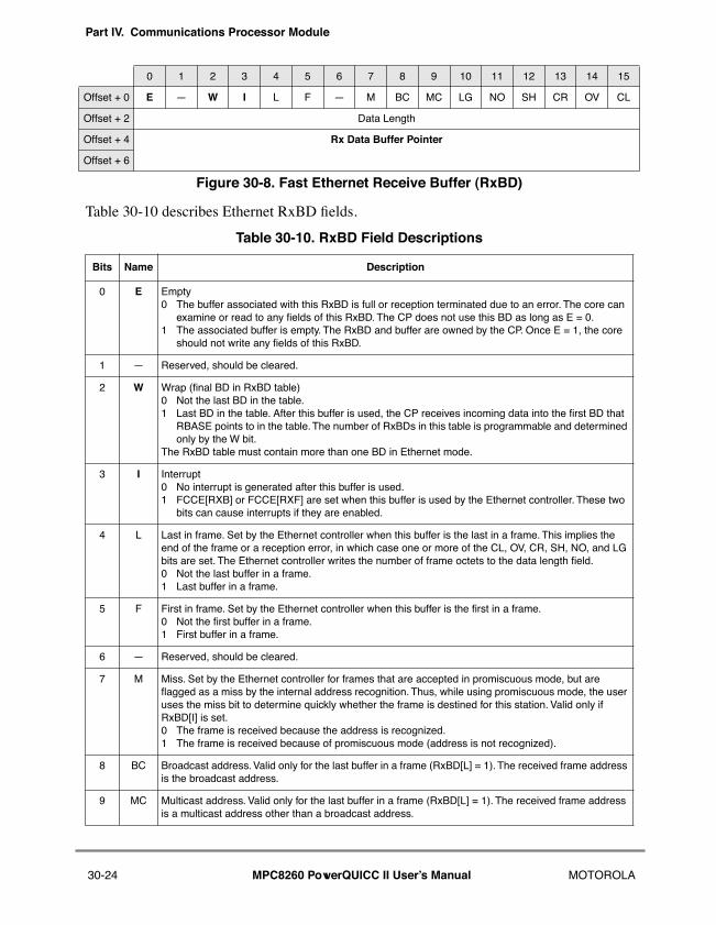
Part IV. Communications Processor Module
Table 30-10 describes Ethernet RxBD Þelds.
0 1 2 3 4 5 6 7 8 9 10 11 12 13 14 15
Offset + 0 E Ñ W I L F Ñ M BC MC LG NO SH CR OV CL
Offset + 2 Data Length
Offset + 4 Rx Data Buffer Pointer
Offset + 6
Figure 30-8. Fast Ethernet Receive Buffer (RxBD)
Table 30-10. RxBD Field Descriptions
Bits Name Description
0 E Empty0 The buffer associated with this RxBD is full or reception terminated due to an error. The core can
examine or read to any Þelds of this RxBD. The CP does not use this BD as long as E = 0.1 The associated buffer is empty. The RxBD and buffer are owned by the CP. Once E = 1, the core
should not write any Þelds of this RxBD.
1 Ñ Reserved, should be cleared.
2 W Wrap (Þnal BD in RxBD table)0 Not the last BD in the table. 1 Last BD in the table. After this buffer is used, the CP receives incoming data into the Þrst BD that
RBASE points to in the table. The number of RxBDs in this table is programmable and determined only by the W bit.
The RxBD table must contain more than one BD in Ethernet mode.
3 I Interrupt 0 No interrupt is generated after this buffer is used. 1 FCCE[RXB] or FCCE[RXF] are set when this buffer is used by the Ethernet controller. These two
bits can cause interrupts if they are enabled.
4 L Last in frame. Set by the Ethernet controller when this buffer is the last in a frame. This implies the end of the frame or a reception error, in which case one or more of the CL, OV, CR, SH, NO, and LG bits are set. The Ethernet controller writes the number of frame octets to the data length Þeld. 0 Not the last buffer in a frame. 1 Last buffer in a frame.
5 F First in frame. Set by the Ethernet controller when this buffer is the Þrst in a frame. 0 Not the Þrst buffer in a frame. 1 First buffer in a frame.
6 Ñ Reserved, should be cleared.
7 M Miss. Set by the Ethernet controller for frames that are accepted in promiscuous mode, but are ßagged as a miss by the internal address recognition. Thus, while using promiscuous mode, the user uses the miss bit to determine quickly whether the frame is destined for this station. Valid only if RxBD[I] is set.0 The frame is received because the address is recognized.1 The frame is received because of promiscuous mode (address is not recognized).
8 BC Broadcast address. Valid only for the last buffer in a frame (RxBD[L] = 1). The received frame address is the broadcast address.
9 MC Multicast address. Valid only for the last buffer in a frame (RxBD[L] = 1). The received frame address is a multicast address other than a broadcast address.
30-24 MPC8260 PowerQUICC II UserÕs Manual MOTOROLA
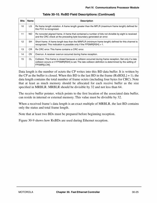
Part IV. Communications Processor Module
Data length is the number of octets the CP writes into this BD data buffer. It is written bythe CP as the buffer is closed. When this BD is the last BD in the frame (RxBD[L] = 1), thedata length contains the total number of frame octets (including four bytes for CRC). Notethat at least as much memory should be allocated for each receive buffer as the sizespeciÞed in MRBLR. MRBLR should be divisible by 32 and not less than 64.
The receive buffer pointer, which points to the Þrst location of the associated data buffer,can reside in internal or external memory. This value must be divisible by 32.
When a received frameÕs data length is an exact multiple of MRBLR, the last BD containsonly the status and total frame length.
Note that at least two BDs must be prepared before beginning reception.
Figure 30-9 shows how RxBDs are used during Ethernet reception.
10 LG Rx frame length violation. A frame length greater than the MFLR (maximum frame length) deÞned for this FCC is recognized.
11 NO Rx nonoctet aligned frame. A frame that contained a number of bits not divisible by eight is received and the CRC check at the preceding byte boundary generated an error.
12 SH Short frame. A frame length less than the MINFLR (minimum frame length) deÞned for this channel is recognized. This indication is possible only if the FPSMR[RSH] = 1.
13 CR Rx CRC error. This frame contains a CRC error.
14 OV Overrun. A receiver overrun occurred during frame reception.
15 CL Collision. This frame is closed because a collision occurred during frame reception. Set only if a late collision occurs or if FPSMR[RSH] is set. The late collision deÞnition is determined by the setting of FPSMR[LCW].
Table 30-10. RxBD Field Descriptions (Continued)
Bits Name Description
MOTOROLA Chapter 30. Fast Ethernet Controller 30-25
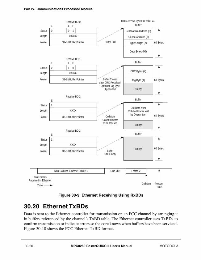
Part IV. Communications Processor Module
Figure 30-9. Ethernet Receiving Using RxBDs
30.20 Ethernet TxBDsData is sent to the Ethernet controller for transmission on an FCC channel by arranging itin buffers referenced by the channelÕs TxBD table. The Ethernet controller uses TxBDs toconÞrm transmission or indicate errors so the core knows when buffers have been serviced.Figure 30-10 shows the FCC Ethernet TxBD format.
Buffer
0
0x0040
32-Bit Buffer Pointer
1
E FReceive BD 0
Status
Length
Pointer
0
0x0045
32-Bit Buffer Pointer
0
E FReceive BD 1
Status
Length
Pointer
1
XXXX
32-Bit Buffer Pointer
EReceive BD 2
Status
Length
Pointer
1
XXXX
32-Bit Buffer Pointer
EReceive BD 3
Status
Length
Pointer
Destination Address (6)
Source Address (6)
Type/Length (2)
Buffer
CRC Bytes (4)
Tag Byte (1)
Buffer
Buffer
Old Data from
Empty
64 Bytes
64 Bytes
64 Bytes
64 Bytes
Two FramesReceived in Ethernet
Collision
Line Idle
PresentTimeTime
Buffer Full
Buffer Closedafter CRC Received.
BufferStill Empty
Empty
MRBLR = 64 Bytes for this FCC
Empty
Data Bytes (50)
Optional Tag Byte
CollisionCauses Bufferto be Reused
0
L
1
L
Frame 2
Collided Frame Willbe Overwritten
Appended
Non-Collided Ethernet Frame 1
30-26 MPC8260 PowerQUICC II UserÕs Manual MOTOROLA
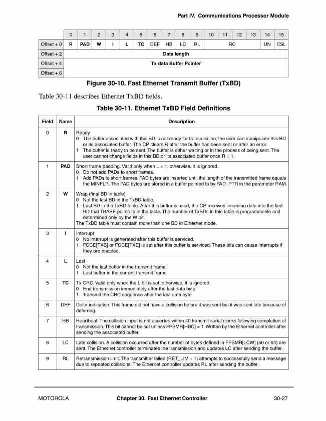
Part IV. Communications Processor Module
Table 30-11 describes Ethernet TxBD Þelds.
0 1 2 3 4 5 6 7 8 9 10 11 12 13 14 15
Offset + 0 R PAD W I L TC DEF HB LC RL RC UN CSL
Offset + 2 Data length
Offset + 4 Tx data Buffer Pointer
Offset + 6
Figure 30-10. Fast Ethernet Transmit Buffer (TxBD)
Table 30-11. Ethernet TxBD Field Definitions
Field Name Description
0 R Ready0 The buffer associated with this BD is not ready for transmission; the user can manipulate this BD
or its associated buffer. The CP clears R after the buffer has been sent or after an error.1 The buffer is ready to be sent. The buffer is either waiting or in the process of being sent. The
user cannot change Þelds in this BD or its associated buffer once R = 1.
1 PAD Short frame padding. Valid only when L = 1; otherwise, it is ignored.0 Do not add PADs to short frames.1 Add PADs to short frames. PAD bytes are inserted until the length of the transmitted frame equals
the MINFLR. The PAD bytes are stored in a buffer pointed to by PAD_PTR in the parameter RAM.
2 W Wrap (Þnal BD in table)0 Not the last BD in the TxBD table. 1 Last BD in the TxBD table. After this buffer is used, the CP receives incoming data into the Þrst
BD that TBASE points to in the table. The number of TxBDs in this table is programmable and determined only by the W bit.
The TxBD table must contain more than one BD in Ethernet mode.
3 I Interrupt 0 No interrupt is generated after this buffer is serviced. 1 FCCE[TXB] or FCCE[TXE] is set after this buffer is serviced. These bits can cause interrupts if
they are enabled.
4 L Last 0 Not the last buffer in the transmit frame.1 Last buffer in the current transmit frame.
5 TC Tx CRC. Valid only when the L bit is set; otherwise, it is ignored.0 End transmission immediately after the last data byte. 1 Transmit the CRC sequence after the last data byte.
6 DEF Defer indication. This frame did not have a collision before it was sent but it was sent late because of deferring.
7 HB Heartbeat. The collision input is not asserted within 40 transmit serial clocks following completion of transmission. This bit cannot be set unless FPSMR[HBC] = 1. Written by the Ethernet controller after sending the associated buffer.
8 LC Late collision. A collision occurred after the number of bytes deÞned in FPSMR[LCW] (56 or 64) are sent. The Ethernet controller terminates the transmission and updates LC after sending the buffer.
9 RL Retransmission limit. The transmitter failed (RET_LIM + 1) attempts to successfully send a message due to repeated collisions. The Ethernet controller updates RL after sending the buffer.
MOTOROLA Chapter 30. Fast Ethernet Controller 30-27
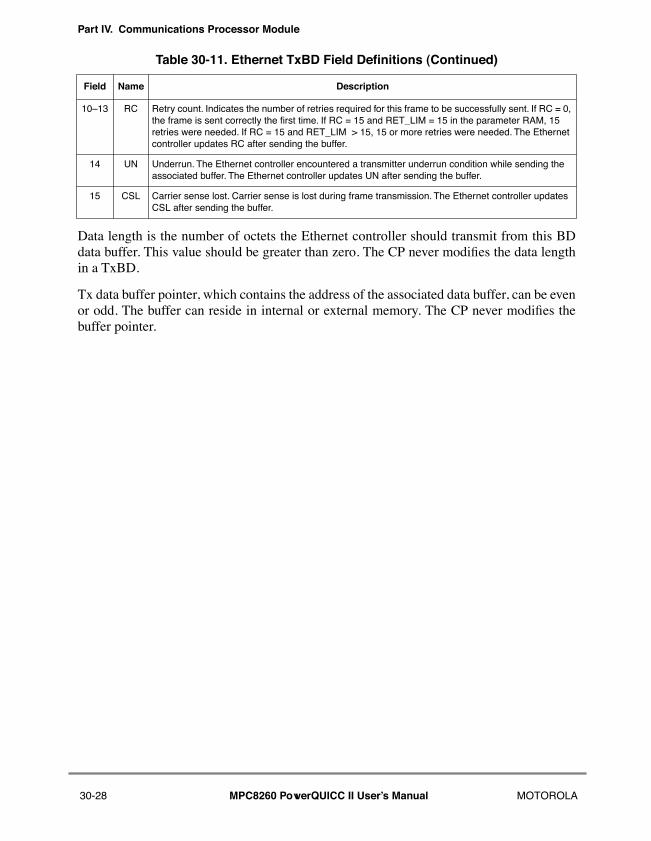
Part IV. Communications Processor Module
Data length is the number of octets the Ethernet controller should transmit from this BDdata buffer. This value should be greater than zero. The CP never modiÞes the data lengthin a TxBD.
Tx data buffer pointer, which contains the address of the associated data buffer, can be evenor odd. The buffer can reside in internal or external memory. The CP never modiÞes thebuffer pointer.
10Ð13 RC Retry count. Indicates the number of retries required for this frame to be successfully sent. If RC = 0, the frame is sent correctly the Þrst time. If RC = 15 and RET_LIM = 15 in the parameter RAM, 15 retries were needed. If RC = 15 and RET_LIM > 15, 15 or more retries were needed. The Ethernet controller updates RC after sending the buffer.
14 UN Underrun. The Ethernet controller encountered a transmitter underrun condition while sending the associated buffer. The Ethernet controller updates UN after sending the buffer.
15 CSL Carrier sense lost. Carrier sense is lost during frame transmission. The Ethernet controller updates CSL after sending the buffer.
Table 30-11. Ethernet TxBD Field Definitions (Continued)
Field Name Description
30-28 MPC8260 PowerQUICC II UserÕs Manual MOTOROLA
Chapter 31 FCC HDLC Controller310310
Layer 2 of the seven-layer OSI model is the data link layer (DLL), in which HDLC is oneof the most common protocols. The framing structure of HDLC is shown in Figure 31-1.HDLC uses a zero insertion/deletion process (commonly known as bit stufÞng) to ensurethat the bit pattern of the delimiter ßag does not occur in the Þelds between ßags. TheHDLC frame is synchronous and therefore relies on the physical layer for a method ofclocking and of synchronizing the transmitter/receiver.
Because the layer 2 frame can be transmitted over a point-to-point link, a broadcastnetwork, or a packet-and-circuit switched system, an address Þeld is needed for the frame'sdestination address. The length of this Þeld is commonly 0, 8, or 16 bits, depending on thedata link layer protocol. For instance, SDLC and LAPB use an 8-bit address and SS#7 hasno address Þeld because it is used always in point-to-point signaling links. LAPD furtherdivides its 16-bit address into different Þelds to specify various access points within onedevice. It also deÞnes a broadcast address. Some HDLC-type protocols also permitextended addressing beyond 16 bits.
The 8- or 16-bit control Þeld provides a ßow-control number and deÞnes the frame type(control or data). The exact use and structure of this Þeld depends upon the protocol usingthe frame. Data is transmitted in the data Þeld, which can vary in length depending uponthe protocol using the frame. Layer 3 frames are carried in this data Þeld.
Error control is implemented by appending a cyclic redundancy check (CRC) to the frame,which in most protocols is 16-bits long but can be as long as 32-bits. In HDLC, the lsb ofeach octet is transmitted Þrst and the msb of the CRC is transmitted Þrst.
When GFMR[MODE] selects HDLC mode, that FCC functions as an HDLC controller.When an FCC in HDLC mode is used with a nonmultiplexed modem interface, the FCCoutputs are connected directly to the external pins. Modem signals can be supportedthrough the appropriate port pins. The receive and transmit clocks can be supplied eitherexternally or from the bank of baud-rate generators. The HDLC controller can also beconnected to one of the TDM channels of the serial interface and used with the TSA. TheHDLC controller consists of separate transmit and receive sections whose operations areasynchronous with the core and can either be synchronous or asynchronous with otherFCCs. The user can allocate external buffer descriptors (BDs) for receive and transmit tasksso many frames can be sent or received without core intervention.
MOTOROLA Chapter 31. FCC HDLC Controller 31-1
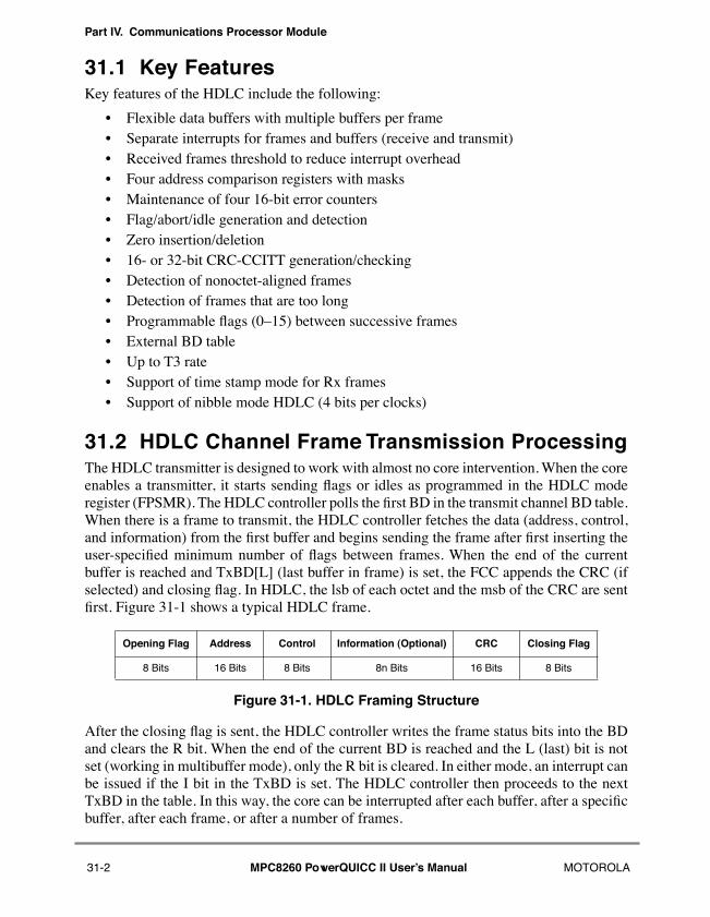
Part IV. Communications Processor Module
31.1 Key FeaturesKey features of the HDLC include the following:
¥ Flexible data buffers with multiple buffers per frame¥ Separate interrupts for frames and buffers (receive and transmit)¥ Received frames threshold to reduce interrupt overhead¥ Four address comparison registers with masks¥ Maintenance of four 16-bit error counters¥ Flag/abort/idle generation and detection¥ Zero insertion/deletion¥ 16- or 32-bit CRC-CCITT generation/checking¥ Detection of nonoctet-aligned frames¥ Detection of frames that are too long¥ Programmable ßags (0Ð15) between successive frames¥ External BD table¥ Up to T3 rate¥ Support of time stamp mode for Rx frames¥ Support of nibble mode HDLC (4 bits per clocks)
31.2 HDLC Channel Frame Transmission ProcessingThe HDLC transmitter is designed to work with almost no core intervention. When the coreenables a transmitter, it starts sending ßags or idles as programmed in the HDLC moderegister (FPSMR). The HDLC controller polls the Þrst BD in the transmit channel BD table.When there is a frame to transmit, the HDLC controller fetches the data (address, control,and information) from the Þrst buffer and begins sending the frame after Þrst inserting theuser-speciÞed minimum number of ßags between frames. When the end of the currentbuffer is reached and TxBD[L] (last buffer in frame) is set, the FCC appends the CRC (ifselected) and closing ßag. In HDLC, the lsb of each octet and the msb of the CRC are sentÞrst. Figure 31-1 shows a typical HDLC frame.
Figure 31-1. HDLC Framing Structure
After the closing ßag is sent, the HDLC controller writes the frame status bits into the BDand clears the R bit. When the end of the current BD is reached and the L (last) bit is notset (working in multibuffer mode), only the R bit is cleared. In either mode, an interrupt canbe issued if the I bit in the TxBD is set. The HDLC controller then proceeds to the nextTxBD in the table. In this way, the core can be interrupted after each buffer, after a speciÞcbuffer, after each frame, or after a number of frames.
Opening Flag Address Control Information (Optional) CRC Closing Flag
8 Bits 16 Bits 8 Bits 8n Bits 16 Bits 8 Bits
31-2 MPC8260 PowerQUICC II UserÕs Manual MOTOROLA
Part IV. Communications Processor Module
To rearrange the transmit queue before the CP has sent all buffers, issue the STOP TRANSMIT
command. This can be useful for sending expedited data before previously linked buffersor for error situations. When receiving the STOP TRANSMIT command, the HDLC controlleraborts the current frame transmission and starts transmitting idles or ßags. When the HDLCcontroller is given the RESTART TRANSMIT command, it resumes transmission. To insert ahigh-priority frame without aborting the current frame, the GRACEFUL STOP TRANSMIT
command can be issued. A special interrupt (GRA) can be generated in the event registerwhen the current frame is complete.
31.3 HDLC Channel Frame Reception ProcessingThe HDLC receiver is designed to work with almost no core intervention and can performaddress recognition, CRC checking, and maximum frame length checking. The receivedframe is available for any HDLC-based protocol. When the core enables a receiver, thereceiver waits for an opening ßag character. When it detects the Þrst byte of the frame, theHDLC controller compares the frame address against the user-programmable addresses.The user has four 16-bit address registers and an address mask available for addressmatching. The HDLC controller compares the received address Þeld to the user-deÞnedvalues after masking with the address mask. The HDLC controller can also detect broadcast(all ones) address frames if one address register is written with all ones.
If a match is detected, the HDLC controller checks the prefetched BD; if it is empty, it startstransferring the incoming frame to the BDÕs associated buffer. When the buffer is full, theHDLC controller clears BD[E] and generates an interrupt if BD[I] = 1. If the incomingframe is larger than the buffer, the HDLC controller fetches the next BD in the table and, ifit is empty, continues transferring the frame to the associated buffer.
During this process, the HDLC controller checks for frames that are too long. When theframe ends, the CRC Þeld is checked against the recalculated value and written to thebuffer. The data length written to the last BD in the HDLC frame is the length of the entireframe. This enables HDLC protocols that lose frames to correctly recognize a frame-too-long condition.
The HDLC controller then sets the last buffer in frame bit, writes the frame status bits intothe BD, and clears the E bit and fetched the next BD. The HDLC controller then generatesa maskable interrupt, indicating that a frame was received and is in memory. The HDLCcontroller then waits for a new frame. Back-to-back frames can be received separated onlyby a single shared ßag.
The user can conÞgure the HDLC controller not to interrupt the core until a speciÞednumber of frames have been received. This is conÞgured in the received frames threshold(RFTHR) location of the parameter RAM. This function can be combined with a timer toimplement a time-out if fewer than the threshold number of frames are received.
MOTOROLA Chapter 31. FCC HDLC Controller 31-3
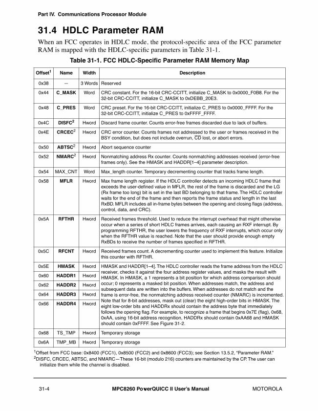
Part IV. Communications Processor Module
31.4 HDLC Parameter RAMWhen an FCC operates in HDLC mode, the protocol-speciÞc area of the FCC parameterRAM is mapped with the HDLC-speciÞc parameters in Table 31-1.
Table 31-1. FCC HDLC-Specific Parameter RAM Memory Map
Offset1
1Offset from FCC base: 0x8400 (FCC1), 0x8500 (FCC2) and 0x8600 (FCC3); see Section 13.5.2, ÒParameter RAM.Ó
Name Width Description
0x38 Ñ 3 Words Reserved
0x44 C_MASK Word CRC constant. For the 16-bit CRC-CCITT, initialize C_MASK to 0x0000_F0B8. For the 32-bit CRC-CCITT, initialize C_MASK to 0xDEBB_20E3.
0x48 C_PRES Word CRC preset. For the 16-bit CRC-CCITT, initialize C_PRES to 0x0000_FFFF. For the 32-bit CRC-CCITT, initialize C_PRES to 0xFFFF_FFFF.
0x4C DISFC2
2DISFC, CRCEC, ABTSC, and NMARCÑThese 16-bit (modulo 216) counters are maintained by the CP. The user can initialize them while the channel is disabled.
Hword Discard frame counter. Counts error-free frames discarded due to lack of buffers.
0x4E CRCEC2 Hword CRC error counter. Counts frames not addressed to the user or frames received in the BSY condition, but does not include overrun, CD lost, or abort errors.
0x50 ABTSC2 Hword Abort sequence counter
0x52 NMARC2 Hword Nonmatching address Rx counter. Counts nonmatching addresses received (error-free frames only). See the HMASK and HADDR[1Ð4] parameter description.
0x54 MAX_CNT Word Max_length counter. Temporary decrementing counter that tracks frame length.
0x58 MFLR Hword Max frame length register. If the HDLC controller detects an incoming HDLC frame that exceeds the user-deÞned value in MFLR, the rest of the frame is discarded and the LG (Rx frame too long) bit is set in the last BD belonging to that frame. The HDLC controller waits for the end of the frame and then reports the frame status and length in the last RxBD. MFLR includes all in-frame bytes between the opening and closing ßags (address, control, data, and CRC).
0x5A RFTHR Hword Received frames threshold. Used to reduce the interrupt overhead that might otherwise occur when a series of short HDLC frames arrives, each causing an RXF interrupt. By programming RFTHR, the user lowers the frequency of RXF interrupts, which occur only when the RFTHR value is reached. Note that the user should provide enough empty RxBDs to receive the number of frames speciÞed in RFTHR.
0x5C RFCNT Hword Received frames count. A decrementing counter used to implement this feature. Initialize this counter with RFTHR.
0x5E HMASK Hword HMASK and HADDR[1Ð4]. The HDLC controller reads the frame address from the HDLC receiver, checks it against the four address register values, and masks the result with HMASK. In HMASK, a 1 represents a bit position for which address comparison should occur; 0 represents a masked bit position. When addresses match, the address and subsequent data are written into the buffers. When addresses do not match and the frame is error-free, the nonmatching address received counter (NMARC) is incremented.Note that for 8-bit addresses, mask out (clear) the eight high-order bits in HMASK. The eight low-order bits and HADDRx should contain the address byte that immediately follows the opening ßag. For example, to recognize a frame that begins 0x7E (ßag), 0x68, 0xAA, using 16-bit address recognition, HADDRx should contain 0xAA68 and HMASK should contain 0xFFFF. See Figure 31-2.
0x60 HADDR1 Hword
0x62 HADDR2 Hword
0x64 HADDR3 Hword
0x66 HADDR4 Hword
0x68 TS_TMP Hword Temporary storage
0x6A TMP_MB Hword Temporary storage
31-4 MPC8260 PowerQUICC II UserÕs Manual MOTOROLA
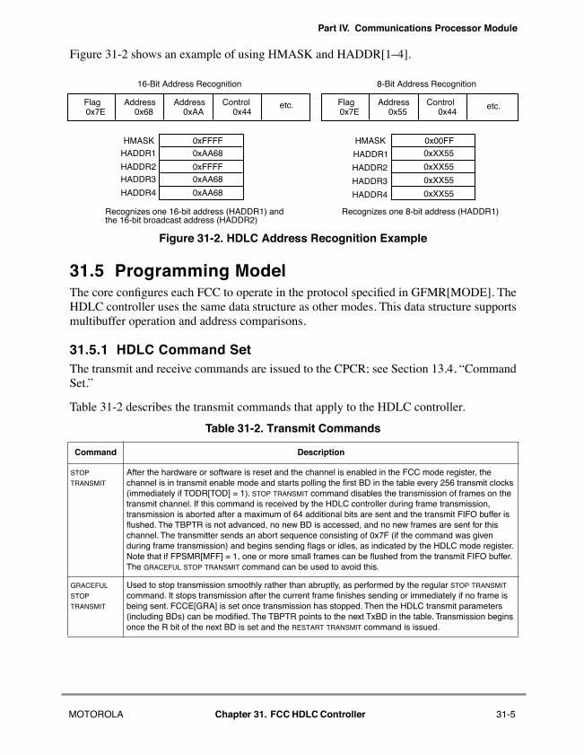
Part IV. Communications Processor Module
Figure 31-2 shows an example of using HMASK and HADDR[1Ð4].
Figure 31-2. HDLC Address Recognition Example
31.5 Programming ModelThe core conÞgures each FCC to operate in the protocol speciÞed in GFMR[MODE]. TheHDLC controller uses the same data structure as other modes. This data structure supportsmultibuffer operation and address comparisons.
31.5.1 HDLC Command SetThe transmit and receive commands are issued to the CPCR; see Section 13.4, ÒCommandSet.Ó
Table 31-2 describes the transmit commands that apply to the HDLC controller.
Table 31-2. Transmit Commands
Command Description
STOP TRANSMIT
After the hardware or software is reset and the channel is enabled in the FCC mode register, the channel is in transmit enable mode and starts polling the Þrst BD in the table every 256 transmit clocks (immediately if TODR[TOD] = 1). STOP TRANSMIT command disables the transmission of frames on the transmit channel. If this command is received by the HDLC controller during frame transmission, transmission is aborted after a maximum of 64 additional bits are sent and the transmit FIFO buffer is ßushed. The TBPTR is not advanced, no new BD is accessed, and no new frames are sent for this channel. The transmitter sends an abort sequence consisting of 0x7F (if the command was given during frame transmission) and begins sending ßags or idles, as indicated by the HDLC mode register. Note that if FPSMR[MFF] = 1, one or more small frames can be ßushed from the transmit FIFO buffer. The GRACEFUL STOP TRANSMIT command can be used to avoid this.
GRACEFUL STOP TRANSMIT
Used to stop transmission smoothly rather than abruptly, as performed by the regular STOP TRANSMIT command. It stops transmission after the current frame Þnishes sending or immediately if no frame is being sent. FCCE[GRA] is set once transmission has stopped. Then the HDLC transmit parameters (including BDs) can be modiÞed. The TBPTR points to the next TxBD in the table. Transmission begins once the R bit of the next BD is set and the RESTART TRANSMIT command is issued.
HMASK
8-Bit Address Recognition
Address 0x68
Control 0x44
Flag 0x7E
Address0xAA
etc.
16-Bit Address Recognition
0xFFFF
0xAA68
0xFFFF
0xAA68
0xAA68
HMASK
Address 0x55
Control 0x44
Flag 0x7E
etc.
0x00FF
0xXX55
0xXX55
0xXX55
0xXX55
HADDR1
HADDR2
HADDR3
HADDR4
HADDR1
HADDR2
HADDR3
HADDR4
Recognizes one 16-bit address (HADDR1) andthe 16-bit broadcast address (HADDR2)
Recognizes one 8-bit address (HADDR1)
MOTOROLA Chapter 31. FCC HDLC Controller 31-5
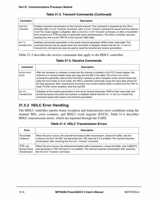
Part IV. Communications Processor Module
Table 31-3 describes the receive commands that apply to the HDLC controller.
31.5.2 HDLC Error Handling The HDLC controller reports frame reception and transmission error conditions using thechannel BDs, error counters, and HDLC event register (FCCE). Table 31-4 describesHDLC transmission errors, which are reported through the TxBD.
RESTART TRANSMIT
Enables character transmission on the transmit channel. This command is expected by the HDLC controller after a STOP TRANSMIT command, after a STOP TRANSMIT command is issued and the channel in its FCC mode register is disabled, after a GRACEFUL STOP TRANSMIT command, or after a transmitter error (underrun or CTS lost with no automatic frame retransmission). The HDLC controller resumes sending from the current TBPTR in the channel TxBD table.
INIT TX PARAMETERS
Initializes all transmit parameters in this serial channel parameter RAM to their reset state. This command should only be issued when the transmitter is disabled. Notice that the INIT TX AND RX PARAMETERS command can also be used to reset the transmit and receive parameters.
Table 31-3. Receive Commands
Command Description
ENTER HUNT MODE
After the hardware or software is reset and the channel is enabled in the FCC mode register, the channel is in receive enable mode and uses the Þrst BD in the table. The ENTER HUNT MODE command is generally used to force the HDLC receiver to abort reception of the current frame and enter the hunt mode. In hunt mode, the HDLC controller continually scans the input data stream for the ßag sequence. After receiving the command, the current receive buffer is closed and the CRC is reset. Further frame reception uses the next BD.
INIT RX PARAMETERS
Initializes all the receive parameters in this serial channel parameter RAM to their reset state and should be issued only when the receiver is disabled. Notice that the INIT TX AND RX PARAMETERS command resets both receive and transmit parameters.
Table 31-4. HDLC Transmission Errors
Error Description
Transmitter Underrun
When this error occurs, the channel terminates buffer transmission, closes the buffer, sets the underrun (U) bit in the BD, and generates the TXE interrupt if it is enabled. The channel resumes transmission after receiving the RESTART TRANSMIT command.
CTS Lost during Frame Transmission
When this error occurs, the channel terminates buffer transmission, closes the buffer, sets TxBD[CT], and generates a TXE interrupt (if it is enabled). The channel resumes transmission after receiving the RESTART TRANSMIT command.
Table 31-2. Transmit Commands (Continued)
Command Description
31-6 MPC8260 PowerQUICC II UserÕs Manual MOTOROLA
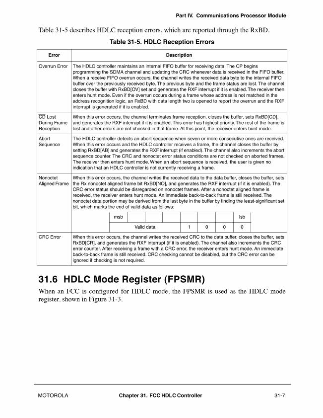
Part IV. Communications Processor Module
Table 31-5 describes HDLC reception errors, which are reported through the RxBD.
31.6 HDLC Mode Register (FPSMR)When an FCC is conÞgured for HDLC mode, the FPSMR is used as the HDLC moderegister, shown in Figure 31-3.
Table 31-5. HDLC Reception Errors
Error Description
Overrun Error The HDLC controller maintains an internal FIFO buffer for receiving data. The CP begins programming the SDMA channel and updating the CRC whenever data is received in the FIFO buffer. When a receive FIFO overrun occurs, the channel writes the received data byte to the internal FIFO buffer over the previously received byte. The previous byte and the frame status are lost. The channel closes the buffer with RxBD[OV] set and generates the RXF interrupt if it is enabled. The receiver then enters hunt mode. Even if the overrun occurs during a frame whose address is not matched in the address recognition logic, an RxBD with data length two is opened to report the overrun and the RXF interrupt is generated if it is enabled.
CD Lost During Frame Reception
When this error occurs, the channel terminates frame reception, closes the buffer, sets RxBD[CD], and generates the RXF interrupt if it is enabled. This error has highest priority. The rest of the frame is lost and other errors are not checked in that frame. At this point, the receiver enters hunt mode.
Abort Sequence
The HDLC controller detects an abort sequence when seven or more consecutive ones are received. When this error occurs and the HDLC controller receives a frame, the channel closes the buffer by setting RxBD[AB] and generates the RXF interrupt (if enabled). The channel also increments the abort sequence counter. The CRC and nonoctet error status conditions are not checked on aborted frames. The receiver then enters hunt mode. When an abort sequence is received, the user is given no indication that an HDLC controller is not currently receiving a frame.
Nonoctet Aligned Frame
When this error occurs, the channel writes the received data to the data buffer, closes the buffer, sets the Rx nonoctet aligned frame bit RxBD[NO], and generates the RXF interrupt (if it is enabled). The CRC error status should be disregarded on nonoctet frames. After a nonoctet aligned frame is received, the receiver enters hunt mode. An immediate back-to-back frame is still received. The nonoctet data portion may be derived from the last byte in the buffer by Þnding the least-signiÞcant set bit, which marks the end of valid data as follows:
msb lsb
Valid data 1 0 0 0
CRC Error When this error occurs, the channel writes the received CRC to the data buffer, closes the buffer, sets RxBD[CR], and generates the RXF interrupt (if it is enabled). The channel also increments the CRC error counter. After receiving a frame with a CRC error, the receiver enters hunt mode. An immediate back-to-back frame is still received. CRC checking cannot be disabled, but the CRC error can be ignored if checking is not required.
MOTOROLA Chapter 31. FCC HDLC Controller 31-7
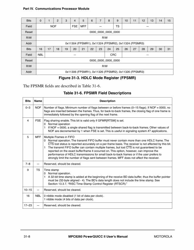
Part IV. Communications Processor Module
The FPSMR Þelds are described in Table 31-6.
Bits 0 1 2 3 4 5 6 7 8 9 10 11 12 13 14 15
Field NOF FSE MFF Ñ TS Ñ
Reset 0000_0000_0000_0000
R/W R/W
Addr 0x11304 (FPSMR1), 0x11324 (FPSMR2), 0x11324 (FPSMR3)
Bits 16 17 18 19 20 21 22 23 24 25 26 27 28 29 30 31
Field NBL Ñ CRC Ñ
Reset 0000_0000_0000_0000
R/W R/W
Addr 0x11306 (FPSMR1), 0x11326 (FPSMR2), 0x11326 (FPSMR3)
Figure 31-3. HDLC Mode Register (FPSMR)
Table 31-6. FPSMR Field Descriptions
Bits Name Description
0Ð3 NOF Number of ßags. Minimum number of ßags between or before frames (0Ð15 ßags). If NOF = 0000, no ßags are inserted between the frames. Thus, for back-to-back frames, the closing ßag of one frame is immediately followed by the opening ßag of the next frame.
4 FSE Flag sharing enable. This bit is valid only if GFMR[RTSM] is set.0 Normal operation1 If NOF = 0000, a single shared ßag is transmitted between back-to-back frames. Other values of
NOF are decremented by 1 when FSE is set. This is useful in signaling system #7 applications.
5 MFF Multiple Frames in FIFO 0 Normal operation. The transmit FIFO buffer must never contain more than one HDLC frame. The
CTS lost status is reported accurately on a per-frame basis. The receiver is not affected by this bit.1 The transmit FIFO buffer can contain multiple frames, but lost CTS is not guaranteed to be
reported on the exact buffer/frame it occurred on. This option, however, can improve the performance of HDLC transmissions for small back-to-back frames or if the user prefers to strongly limit the number of ßags sent between frames. MFF does not affect the receiver.
7Ð8 Ñ Reserved, should be cleared.
9 TS Time stamp0 Normal operation.1 A 32-bit time stamp is added at the beginning of the receive BD data buffer, thus the buffer pointer
must be (32-byte aligned - 4). The BDÕs data length does not include the time stamp. See Section 13.3.7, ÒRISC Time-Stamp Control Register (RTSCR).Ó
10Ð15 Ñ Reserved, should be cleared.
16 NBL 0 nibble mode disabled (1 bit of data per clock).1 nibble mode (4 bits of data per clock).
17Ð23 Ñ Reserved, should be cleared.
31-8 MPC8260 PowerQUICC II UserÕs Manual MOTOROLA
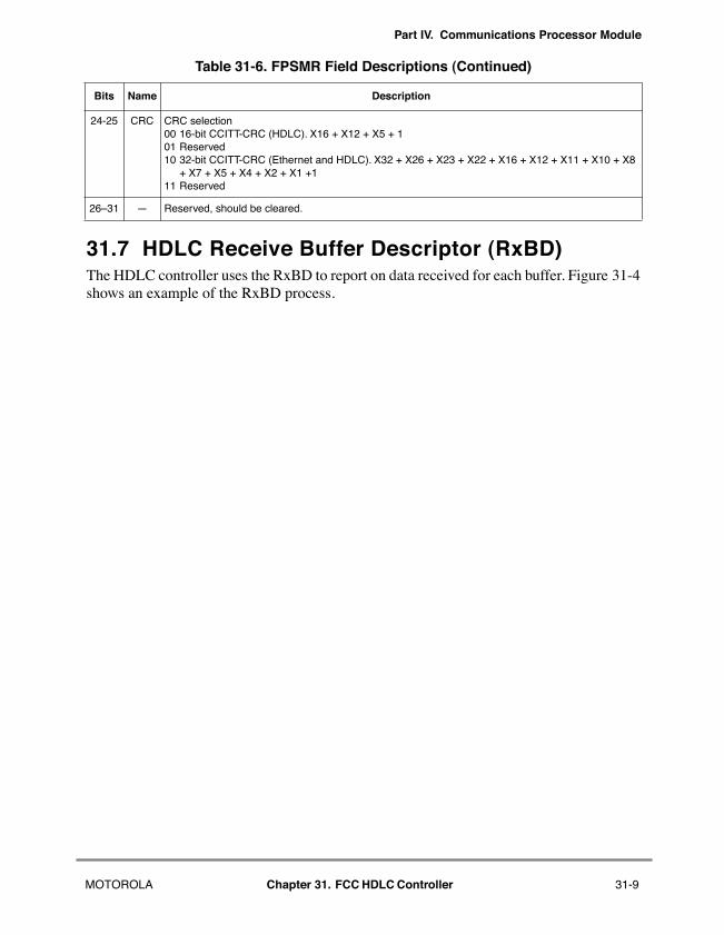
Part IV. Communications Processor Module
31.7 HDLC Receive Buffer Descriptor (RxBD)The HDLC controller uses the RxBD to report on data received for each buffer. Figure 31-4shows an example of the RxBD process.
24-25 CRC CRC selection00 16-bit CCITT-CRC (HDLC). X16 + X12 + X5 + 101 Reserved10 32-bit CCITT-CRC (Ethernet and HDLC). X32 + X26 + X23 + X22 + X16 + X12 + X11 + X10 + X8
+ X7 + X5 + X4 + X2 + X1 +111 Reserved
26Ð31 Ñ Reserved, should be cleared.
Table 31-6. FPSMR Field Descriptions (Continued)
Bits Name Description
MOTOROLA Chapter 31. FCC HDLC Controller 31-9
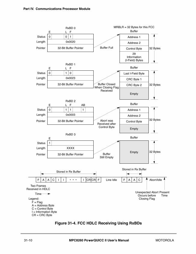
Part IV. Communications Processor Module
Figure 31-4. FCC HDLC Receiving Using RxBDs
Buffer
0
0x0020
32-Bit Buffer Pointer
1
E FRxBD 0
Status
Length
Pointer
0
0x0023
32-Bit Buffer Pointer
0
E FRxBD 1
Status
Length
Pointer
0
0x0003
32-Bit Buffer Pointer
1
E FRxBD 2
Status
Length
Pointer
1
XXXX
32-Bit Buffer Pointer
ERxBD 3
Status
Length
Pointer
Address 1
Address 2
Control Byte
Buffer
CRC Byte 1
CRC Byte 2
Buffer
Address 1
Address 2
Buffer
Control Byte
Empty
32 Bytes
32 Bytes
32 Bytes
32 Bytes
Two FramesReceived in HDLC
Unexpected Abort
Stored in Rx Buffer
Line Idle
Occurs beforePresent
TimeTime
Stored in Rx Buffer
Buffer Full
Buffer ClosedWhen Closing Flag
BufferStill Empty
1
AB
29
Empty
MRBLR = 32 Bytes for this FCC
Empty
Last I-Field Byte
Information(I-Field) Bytes
Received
Abort wasReceived afterControl Byte
0
L
1
L
1
L
F A A C I I I CR CR F
Closing Flag
Abort/IdleF A A C
Legend:F = FlagA = Address ByteC = Control ByteI = Information ByteCR = CRC Byte
. . .
31-10 MPC8260 PowerQUICC II UserÕs Manual MOTOROLA
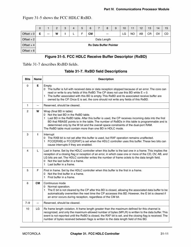
Part IV. Communications Processor Module
Figure 31-5 shows the FCC HDLC RxBD.
Table 31-7 describes RxBD Þelds.
0 1 2 3 4 5 6 7 8 9 10 11 12 13 14 15
Offset + 0 E Ñ W I L F CM Ñ LG NO AB CR OV CD
Offset + 2 Data Length
Offset + 4 Rx Data Buffer Pointer
Offset + 6
Figure 31-5. FCC HDLC Receive Buffer Descriptor (RxBD)
Table 31-7. RxBD field Descriptions
Bits Name Description
0 E Empty0 The buffer is full with received data or data reception stopped because of an error. The core can
read or write to any Þelds of this RxBD. The CP does not use this BD while E = 0.1 The buffer associated with this BD is empty. This RxBD and its associated receive buffer are
owned by the CP. Once E is set, the core should not write any Þelds of this RxBD.
1 Ñ Reserved, should be cleared.
2 W Wrap (Þnal BD in table)0 Not the last BD in the RxBD table. 1 Last BD in the RxBD table. After this buffer is used, the CP receives incoming data into the Þrst
BD that RBASE points to in the table. The number of RxBDs in this table is programmable and is determined only by the W bit and the overall space constraints of the dual-port RAM.
The RxBD table must contain more than one BD in HDLC mode.
3 I Interrupt0 The RXB bit is not set after this buffer is used, but RXF operation remains unaffected.1 FCCE[RXB] or FCCE[RXF] is set when the HDLC controller uses this buffer. These two bits can
cause interrupts if they are enabled.
4 L Last in frame. Set by the HDLC controller when this buffer is the last one in a frame. This implies the reception of a closing ßag or reception of an error, in which case one or more of the CD, OV, AB, and LG bits are set. The HDLC controller writes the number of frame octets to the data length Þeld. 0 Not the last buffer in a frame. 1 Last buffer in a frame.
5 F First in frame. Set by the HDLC controller when this buffer is the Þrst in a frame. 0 Not the Þrst buffer in a frame. 1 First buffer in a frame.
6 CM Continuous mode0 Normal operation.1 The E bit is not cleared by the CP after this BD is closed, allowing the associated data buffer to be
automatically overwritten the next time the CP accesses this BD. However, the E bit is cleared if an error occurs during reception, regardless of the CM bit.
7Ð9 Ñ Reserved, should be cleared.
10 LG Rx frame length violation. A frame length greater than the maximum deÞned for this channel is recognized, and only the maximum-allowed number of bytes (MFLR) is written to the data buffer. This event is not reported until the RxBD is closed, the RXF bit is set, and the closing ßag is received. The number of bytes received between ßags is written to the data length Þeld of this BD.
MOTOROLA Chapter 31. FCC HDLC Controller 31-11
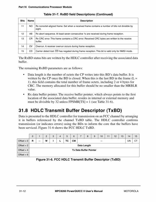
Part IV. Communications Processor Module
The RxBD status bits are written by the HDLC controller after receiving the associated databuffer.
The remaining RxBD parameters are as follows:
¥ Data length is the number of octets the CP writes into this BDÕs data buffer. It is written by the CP once the BD is closed. When this is the last BD in the frame (L = 1), this Þeld contains the total number of frame octets, including 2 or 4 bytes for CRC. The memory allocated for this buffer should be no smaller than the MRBLR value.
¥ Rx data buffer pointer. The receive buffer pointer, which always points to the Þrst location of the associated data buffer, resides in internal or external memory and must be divisible by 32 unless FPSMR[TS] = 1 (see Table 31-6).
31.8 HDLC Transmit Buffer Descriptor (TxBD)Data is presented to the HDLC controller for transmission on an FCC channel by arrangingit in buffers referenced by the channel TxBD table. The HDLC controller conÞrmstransmission (or indicates errors) using the BDs to inform the core that the buffers havebeen serviced. Figure 31-6 shows the FCC HDLC TxBD.
11 NO Rx nonoctet-aligned frame. Set when a received frame contains a number of bits not divisible by eight.
12 AB Rx abort sequence. At least seven consecutive 1s are received during frame reception.
13 CR Rx CRC error. This frame contains a CRC error. Received CRC bytes are written to the receive buffer.
14 OV Overrun. A receiver overrun occurs during frame reception.
15 CD Carrier detect lost. CD has negated during frame reception. This bit is valid only for NMSI mode.
0 1 2 3 4 5 6 7 8 9 10 11 12 13 14 15
Offset + 0 R Ñ W I L TC CM Ñ UN CT
Offset + 2 Data Length
Offset + 4 Tx Data Buffer Pointer
Offset + 6
Figure 31-6. FCC HDLC Transmit Buffer Descriptor (TxBD)
Table 31-7. RxBD field Descriptions (Continued)
Bits Name Description
31-12 MPC8260 PowerQUICC II UserÕs Manual MOTOROLA
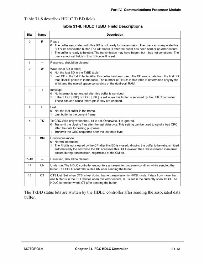
Part IV. Communications Processor Module
Table 31-8 describes HDLC TxBD Þelds.
The TxBD status bits are written by the HDLC controller after sending the associated databuffer.
Table 31-8. HDLC TxBD Field Descriptions
Bits Name Description
0 R Ready0 The buffer associated with this BD is not ready for transmission. The user can manipulate this
BD or its associated buffer. The CP clears R after the buffer has been sent or an error occurs.1 The buffer is ready to be sent. The transmission may have begun, but it has not completed. The
user cannot set Þelds in this BD once R is set.
1 Ñ Reserved, should be cleared.
2 W Wrap (Þnal BD in table)0 Not the last BD in the TxBD table. 1 Last BD in the TxBD table. After this buffer has been used, the CP sends data from the Þrst BD
that TBASE points to in the table. The number of TxBDs in this table is determined only by the W bit and the overall space constraints of the dual-port RAM.
3 I Interrupt0 No interrupt is generated after this buffer is serviced.1 Either FCCE[TXB] or FCCE[TXE] is set when this buffer is serviced by the HDLC controller.
These bits can cause interrupts if they are enabled.
4 L Last 0 Not the last buffer in the frame. 1 Last buffer in the current frame.
5 TC Tx CRC.Valid only when the L bit is set. Otherwise, it is ignored.0 Transmit the closing ßag after the last data byte. This setting can be used to send a bad CRC
after the data for testing purposes. 1 Transmit the CRC sequence after the last data byte.
6 CM Continuous mode0 Normal operation.1 The R bit is not cleared by the CP after this BD is closed, allowing the buffer to be retransmitted
automatically the next time the CP accesses this BD. However, the R bit is cleared if an error occurs during transmission, regardless of the CM bit.
7Ð13 Ñ Reserved, should be cleared.
14 UN Underrun. The HDLC controller encounters a transmitter underrun condition while sending the buffer. The HDLC controller writes UN after sending the buffer.
15 CT CTS lost. Set when CTS is lost during frame transmission in NMSI mode. If data from more than one buffer is in the FIFO buffer when this error occurs, CT is set in the currently open TxBD. The HDLC controller writes CT after sending the buffer.
MOTOROLA Chapter 31. FCC HDLC Controller 31-13
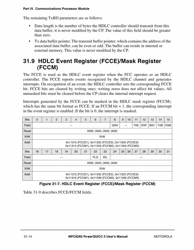
Part IV. Communications Processor Module
The remaining TxBD parameters are as follows:
¥ Data length is the number of bytes the HDLC controller should transmit from this data buffer; it is never modiÞed by the CP. The value of this Þeld should be greater than zero.
¥ Tx data buffer pointer. The transmit buffer pointer, which contains the address of the associated data buffer, can be even or odd. The buffer can reside in internal or external memory. This value is never modiÞed by the CP.
31.9 HDLC Event Register (FCCE)/Mask Register (FCCM)
The FCCE is used as the HDLC event register when the FCC operates as an HDLCcontroller. The FCCE reports events recognized by the HDLC channel and generatesinterrupts. On recognition of an event, the HDLC controller sets the corresponding FCCEbit. FCCE bits are cleared by writing ones; writing zeros does not affect bit values. Allunmasked bits must be cleared before the CP clears the internal interrupt request.
Interrupts generated by the FCCE can be masked in the HDLC mask register (FCCM),which has the same bit format as FCCE. If an FCCM bit = 1, the corresponding interruptin the event register is enabled. If the bit is 0, the interrupt is masked.
Table 31-9 describes FCCE/FCCM Þelds.
Bits 0 1 2 3 4 5 6 7 8 9 10 11 12 13 14 15
Field Ñ GRA Ñ TXE RXF BSY TXB RXB
Reset 0000_0000_0000_0000
R/W R/W
Addr 0x11310 (FCCE1), 0x11330 (FCCE2), 0x11350 (FCCE3)/0x11314 (FCCM1), 0x11334 (FCCM2), 0x11354 (FCCM3)
Bits 16 17 18 19 20 21 22 23 24 25 26 27 28 29 30 31
Field Ñ FLG IDL Ñ
Reset 0000_0000_0000_0000
R/W R/W
Addr 0x11312 (FCCE1), 0x11332 (FCCE2), 0x11352 (FCCE3)/0x11316 (FCCM1), 0x11336 (FCCM2), 0x11356 (FCCM3)
Figure 31-7. HDLC Event Register (FCCE)/Mask Register (FCCM)
31-14 MPC8260 PowerQUICC II UserÕs Manual MOTOROLA
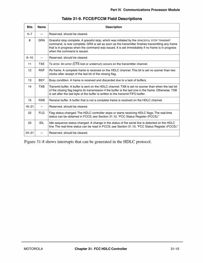
Part IV. Communications Processor Module
Figure 31-8 shows interrupts that can be generated in the HDLC protocol.
Table 31-9. FCCE/FCCM Field Descriptions
Bits Name Description
0Ð7 Ñ Reserved, should be cleared.
8 GRA Graceful stop complete. A graceful stop, which was initiated by the GRACEFUL STOP TRANSMIT command, is now complete. GRA is set as soon as the transmitter Þnishes transmitting any frame that is in progress when the command was issued. It is set immediately if no frame is in progress when the command is issued.
9Ð10 Ñ Reserved, should be cleared.
11 TXE Tx error. An error (CTS lost or underrun) occurs on the transmitter channel.
12 RXF Rx frame. A complete frame is received on the HDLC channel. This bit is set no sooner than two clocks after receipt of the last bit of the closing ßag.
13 BSY Busy condition. A frame is received and discarded due to a lack of buffers.
14 TXB Transmit buffer. A buffer is sent on the HDLC channel. TXB is set no sooner than when the last bit of the closing ßag begins its transmission if the buffer is the last one in the frame. Otherwise, TXB is set after the last byte of the buffer is written to the transmit FIFO buffer.
15 RXB Receive buffer. A buffer that is not a complete frame is received on the HDLC channel.
16Ð21 Ñ Reserved, should be cleared.
22 FLG Flag status changed. The HDLC controller stops or starts receiving HDLC ßags. The real-time status can be obtained in FCCS; see Section 31.10, ÒFCC Status Register (FCCS).Ó
23 IDL Idle sequence status changed. A change in the status of the serial line is detected on the HDLC line. The real-time status can be read in FCCS; see Section 31.10, ÒFCC Status Register (FCCS).Ó
24Ð31 Ñ Reserved, should be cleared.
MOTOROLA Chapter 31. FCC HDLC Controller 31-15
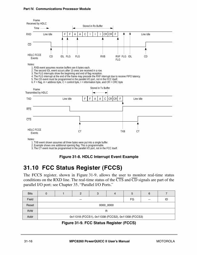
Part IV. Communications Processor Module
Figure 31-8. HDLC Interrupt Event Example
31.10 FCC Status Register (FCCS) The FCCS register, shown in Figure 31-9, allows the user to monitor real-time statusconditions on the RXD line. The real-time status of the CTS and CD signals are part of theparallel I/O port; see Chapter 35, ÒParallel I/O Ports.Ó
Bits 0 1 2 3 4 5 6 7
Field Ñ FG Ñ ID
Reset 0000_0000
R/W R
Addr 0x11318 (FCCS1), 0x11338 (FCCS2), 0x11358 (FCCS3)
Figure 31-9. FCC Status Register (FCCS)
CD IDL FLG RXB RXF IDL CD
Line Idle
Stored in Rx Buffer
RXD
CD
FrameReceived by HDLC
Time
Line Idle
TXD
RTS
FrameTransmitted by HDLC
CTS
TXB CTCT
Line Idle Line Idle
Stored in Tx Buffer
Notes:
HDLC FCCEEvents
1. RXB event assumes receive buffers are 6 bytes each.2. The second IDL event occurs after 15 ones are received in a row.3. The FLG interrupts show the beginning and end of flag reception.4. The FLG interrupt at the end of the frame may precede the RXF interrupt due to receive FIFO latency.5. The CD event must be programmed in the parallel I/O port, not in the FCC itself.
Notes:
HDLC FCCEEvents
1. TXB event shown assumes all three bytes were put into a single buffer.2. Example shows one additional opening flag. This is programmable.
FF A A C I I I CR CR F
FLG FLGFLG
6. F = flag, A = address byte, C = control byte, I = information byte, and CR = CRC byte
F F A A C CR CR F
3. The CT event must be programmed in the parallel I/O port, not in the FCC itself.
31-16 MPC8260 PowerQUICC II UserÕs Manual MOTOROLA
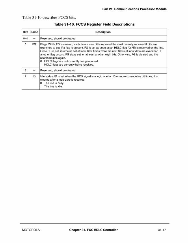
Part IV. Communications Processor Module
Table 31-10 describes FCCS bits.
Table 31-10. FCCS Register Field Descriptions
Bits Name Description
0Ð4 Ñ Reserved, should be cleared.
5 FG Flags. While FG is cleared, each time a new bit is received the most recently received 8 bits are examined to see if a ßag is present. FG is set as soon as an HDLC ßag (0x7E) is received on the line. Once FG is set, it remains set at least 8 bit times while the next 8 bits of input data are examined. If another ßag occurs, FG stays set for at least another eight bits. Otherwise, FG is cleared and the search begins again. 0 HDLC ßags are not currently being received.1 HDLC ßags are currently being received.
6 Ñ Reserved, should be cleared.
7 ID Idle status. ID is set when the RXD signal is a logic one for 15 or more consecutive bit times; it is cleared after a logic zero is received.0 The line is busy.1 The line is idle.
MOTOROLA Chapter 31. FCC HDLC Controller 31-17
Part IV. Communications Processor Module
31-18 MPC8260 PowerQUICC II UserÕs Manual MOTOROLA
Chapter 32 FCC Transparent Controller 320320
The FCC transparent controller functions as a high-speed serial-to-parallel and parallel-to-serial converter. Transparent mode provides a clear channel on which the FCC performs nobit-level manipulationÑimplementing higher-level protocols would require software.Transparent mode is also referred to as a totally transparent or promiscuous operation.
Basic applications for an FCC in transparent mode include the following:
¥ For data, such as voice, moving serially without the need for protocol processing
¥ For board-level applications, such as chip-to-chip communications, requiring a serial-to-parallel and parallel-to-serial conversion
¥ For applications requiring the switching of data paths without altering the protocol encoding itself, such as a multiplexer in which data from a high-speed TDM serial stream is divided into multiple low-speed data streams
An FCC transmitter and receiver can be programmed in transparent mode independently.Setting GFMRx[TTx] enables the transparent transmitter; setting GFMRx[TRx] enablesthe transparent receiver. Both bits must be set for full-duplex transparent operation. If onlyone bit is set, the other half of the FCC operates with the protocol programmed inGFMRx[MODE]. This allows loopback modes to transfer data from one memory locationto another (using DMA) while the data is converted to a speciÞc serial format. However,the Ethernet and ATM controllers cannot be split in this way. See Section 28.2, ÒGeneralFCC Mode Registers (GFMRx).Ó
The FCC in transparent mode can work with the TSA or NMSI and support modem linesusing the general-purpose I/O signals. The data can be transmitted and received with msbor lsb Þrst in each octet. The FCC consists of separate transmit and receive sections whoseoperations are asynchronous with the core and can either be synchronous or asynchronouswith respect to the other FCCs. Each clock can be supplied from the internal BRG bank orexternal signals.
MOTOROLA Chapter 32. FCC Transparent Controller 32-1
Part IV. Communications Processor Module
32.1 FeaturesThe following is a list of the transparent controllerÕs important features:
¥ Flexible data buffers
¥ Automatic SYNC detection on receive
Ñ 16-bit pattern
Ñ 8-bit pattern
Ñ Automatic sync (always synchronized)
Ñ External sync signal support
¥ CRCs can optionally be transmitted and received
¥ Reverse data mode
¥ Another protocol can be performed on the FCCÕs other half (transmitter or receiver) during transparent mode
¥ External BD table
32.2 Transparent Channel OperationThe transparent transmitter and receiver operates in the same way as the HDLC controllerof the FCC (see Chapter 31, ÒFCC HDLC ControllerÓ) except in the following ways:
1. The FPSMR does not affect the transparent controller, only the GFMR does.
2. In Table 31-1, MFLR, HMASK, RFTHR, and RFCNT must be cleared for proper operation of the transparent receiver.
3. Transmitter synchronization has to be achieved using CTS before the transmitter begins sending; see Section 32.3, ÒAchieving Synchronization in Transparent Mode.Ó
32.3 Achieving Synchronization in Transparent ModeOnce the FCC transmitter is enabled for transparent operation in the GFMR, the TxBD isprepared for the FCC, and the transmit FIFO is preloaded by the SDMA channel, anotherprocess must occur before data can be transmitted. It is called transmit synchronization.
Similarly, once the FCC receiver is enabled for transparent operation in the GFMR and theRxBD is made empty for the FCC, receive synchronization must occur before data can bereceived. The synchronization process gives the user bit-level control of when thetransmission and reception begins. The methods for this are as follows:
¥ An in-line synchronization pattern
¥ External synchronization signals
¥ Automatic sync
32-2 MPC8260 PowerQUICC II UserÕs Manual MOTOROLA
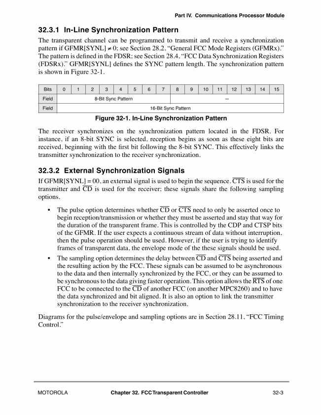
Part IV. Communications Processor Module
32.3.1 In-Line Synchronization PatternThe transparent channel can be programmed to transmit and receive a synchronizationpattern if GFMR[SYNL] ¹ 0; see Section 28.2, ÒGeneral FCC Mode Registers (GFMRx).ÓThe pattern is deÞned in the FDSR; see Section 28.4, ÒFCC Data Synchronization Registers(FDSRx).Ó GFMR[SYNL] deÞnes the SYNC pattern length. The synchronization patternis shown in Figure 32-1.
The receiver synchronizes on the synchronization pattern located in the FDSR. Forinstance, if an 8-bit SYNC is selected, reception begins as soon as these eight bits arereceived, beginning with the Þrst bit following the 8-bit SYNC. This effectively links thetransmitter synchronization to the receiver synchronization.
32.3.2 External Synchronization SignalsIf GFMR[SYNL] = 00, an external signal is used to begin the sequence. CTS is used for thetransmitter and CD is used for the receiver; these signals share the following samplingoptions.
¥ The pulse option determines whether CD or CTS need to only be asserted once to begin reception/transmission or whether they must be asserted and stay that way for the duration of the transparent frame. This is controlled by the CDP and CTSP bits of the GFMR. If the user expects a continuous stream of data without interruption, then the pulse operation should be used. However, if the user is trying to identify frames of transparent data, the envelope mode of the these signals should be used.
¥ The sampling option determines the delay between CD and CTS being asserted and the resulting action by the FCC. These signals can be assumed to be asynchronous to the data and then internally synchronized by the FCC, or they can be assumed to be synchronous to the data giving faster operation. This option allows the RTS of one FCC to be connected to the CD of another FCC (on another MPC8260) and to have the data synchronized and bit aligned. It is also an option to link the transmitter synchronization to the receiver synchronization.
Diagrams for the pulse/envelope and sampling options are in Section 28.11, ÒFCC TimingControl.Ó
Bits 0 1 2 3 4 5 6 7 8 9 10 11 12 13 14 15
Field 8-Bit Sync Pattern Ñ
Field 16-Bit Sync Pattern
Figure 32-1. In-Line Synchronization Pattern
MOTOROLA Chapter 32. FCC Transparent Controller 32-3
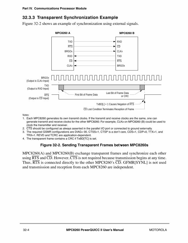
Part IV. Communications Processor Module
32.3.3 Transparent Synchronization ExampleFigure 32-2 shows an example of synchronization using external signals.
Figure 32-2. Sending Transparent Frames between MPC8260s
MPC8260(A) and MPC8260(B) exchange transparent frames and synchronize each otherusing RTS and CD. However, CTS is not required because transmission begins at any time.Thus, RTS is connected directly to the other MPC8260Õs CD. GFMR[SYNL] is not usedand transmission and reception from each MPC8260 are independent.
RXD
CD
CLKx
TXD
RTSCD
RXD
BRGOx
RTS
TXD
CLKx BRGOx
BRGOx
Last Bit of Frame DataFirst Bit of Frame Data
(Output is CLKx Input)
TXD(Output is RXD Input)
RTS(Output is CD Input)
or CRC
TxBD[L] = 1 Causes Negation of RTS
CD Lost Condition Terminates Reception of Frame
MPC8260 A MPC8260 B
Notes:1. Each MPC8260 generates its own transmit clocks. If the transmit and receive clocks are the same, one can
generate transmit and receive clocks for the other MPC8260. For example, CLKx on MPC8260 (B) could be used to clock the transmitter and receiver.
2. CTS should be conÞgured as always asserted in the parallel I/O port or connected to ground externally.3. The required GSMR conÞgurations are DIAG= 00, CTSS=1, CTSP is a donÕt care, CDS=1, CDP=0, TTX=1, and
TRX=1. REVD and TCRC are application-dependent.4. The transparent frame contains a CRC if TxBD[TC] is set.
32-4 MPC8260 PowerQUICC II UserÕs Manual MOTOROLA
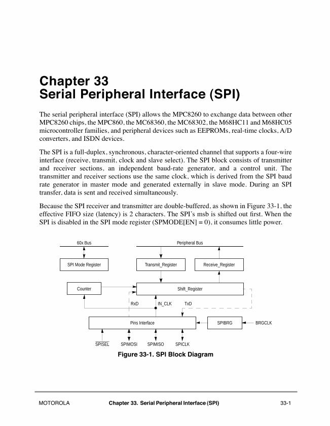
Chapter 33 Serial Peripheral Interface (SPI)330330
The serial peripheral interface (SPI) allows the MPC8260 to exchange data between otherMPC8260 chips, the MPC860, the MC68360, the MC68302, the M68HC11 and M68HC05microcontroller families, and peripheral devices such as EEPROMs, real-time clocks, A/Dconverters, and ISDN devices.
The SPI is a full-duplex, synchronous, character-oriented channel that supports a four-wireinterface (receive, transmit, clock and slave select). The SPI block consists of transmitterand receiver sections, an independent baud-rate generator, and a control unit. Thetransmitter and receiver sections use the same clock, which is derived from the SPI baudrate generator in master mode and generated externally in slave mode. During an SPItransfer, data is sent and received simultaneously.
Because the SPI receiver and transmitter are double-buffered, as shown in Figure 33-1, theeffective FIFO size (latency) is 2 characters. The SPIÕs msb is shifted out Þrst. When theSPI is disabled in the SPI mode register (SPMODE[EN] = 0), it consumes little power.
Figure 33-1. SPI Block Diagram
SPI Mode Register Transmit_Register Receive_Register
Counter Shift_Register
SPIBRGPins Interface BRGCLK
SPIMOSISPISEL SPIMISO SPICLK
TxDRxD IN_CLK
60x Bus Peripheral Bus
MOTOROLA Chapter 33. Serial Peripheral Interface (SPI) 33-1
Part IV. Communications Processor Module
33.1 FeaturesThe following is a list of the SPIÕs main features:
¥ Four-signal interface (SPIMOSI, SPIMISO, SPICLK, and SPISEL) multiplexed with Port B signals
¥ Full-duplex operation¥ Works with data characters from 4 to 16 bits long¥ Supports back-to-back character transmission and reception¥ Master or slave SPI modes supported¥ Multimaster environment support¥ Continuous transfer mode for automatic scanning of a peripheral¥ Supports maximum clock rates of 25 in master mode and 50 MHz in slave mode,
assuming a 100-MHz system clock¥ Independent programmable baud rate generator¥ Programmable clock phase and polarity¥ Open-drain outputs support multimaster conÞguration¥ Local loopback capability for testing
33.2 SPI Clocking and Signal FunctionsThe SPI can be conÞgured as a slave or as a master in single- or multiple-masterenvironments. The master SPI generates the transfer clock SPICLK using the SPI baud rategenerator (BRG). The SPI BRG takes its input from BRGCLK, which is generated in theMPC8260 clock synthesizer.
SPICLK is a gated clock, active only during data transfers. Four combinations of SPICLKphase and polarity can be conÞgured with SPMODE[CI, CP]. SPI signals can also beconÞgured as open-drain to support a multimaster conÞguration in which a shared SPIsignal is driven by the MPC8260 or an external SPI device.
The SPI master-in slave-out SPIMISO signal acts as an input for master devices and as anoutput for slave devices. Conversely, the master-out slave-in SPIMOSI signal is an outputfor master devices and an input for slave devices. The dual functionality of these signalsallows the SPIs in a multimaster environment to communicate with one another using acommon hardware conÞguration.
¥ When the SPI is a master, SPICLK is the clock output signal that shifts received data in from SPIMISO and transmitted data out to SPIMOSI. SPI masters must output a slave select signal to enable SPI slave devices by using a separate general-purpose I/O signal. Assertion of an SPIÕs SPISEL while it is master causes an error.
33-2 MPC8260 PowerQUICC II UserÕs Manual MOTOROLA
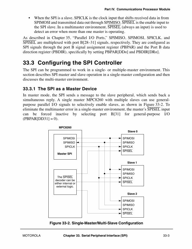
Part IV. Communications Processor Module
¥ When the SPI is a slave, SPICLK is the clock input that shifts received data in from SPIMOSI and transmitted data out through SPIMISO. SPISEL is the enable input to the SPI slave. In a multimaster environment, SPISEL (always an input) is used to detect an error when more than one master is operating.
As described in Chapter 35, ÒParallel I/O Ports,Ó SPIMISO, SPIMOSI, SPICLK, andSPISEL are multiplexed with port B[28Ð31] signals, respectively. They are conÞgured asSPI signals through the port B signal assignment register (PBPAR) and the Port B datadirection register (PBDIR), speciÞcally by setting PBPAR[DDn] and PBDIR[DRn].
33.3 ConÞguring the SPI ControllerThe SPI can be programmed to work in a single- or multiple-master environment. Thissection describes SPI master and slave operation in a single-master conÞguration and thendiscusses the multi-master environment.
33.3.1 The SPI as a Master DeviceIn master mode, the SPI sends a message to the slave peripheral, which sends back asimultaneous reply. A single master MPC8260 with multiple slaves can use general-purpose parallel I/O signals to selectively enable slaves, as shown in Figure 33-2. Toeliminate the multimaster error in a single-master environment, the masterÕs SPISEL inputcan be forced inactive by selecting port B[31] for general-purpose I/O(PBPAR[DD31] = 0).
Figure 33-2. Single-Master/Multi-Slave Configuration
SPIMOSI
SPIMISO
SPICLK
SPISEL
Slave 0
SPIMISO
SPICLK
SPISEL
Slave 1
Slave 2
Master SPI
SPIMOSI
SPIMISO
SPICLK
SPISEL
SPIMOSI
The SPISEL
SPICLK
SPIMISO
SPIMOSI
MPC8260
decoder can beeither internal orexternal logic.
MOTOROLA Chapter 33. Serial Peripheral Interface (SPI) 33-3
Part IV. Communications Processor Module
To start exchanging data, the core writes the data to be sent into a buffer, conÞgures a TxBDwith TxBD[R] set, and conÞgures one or more RxBDs. The core then sets SPCOM[STR]in the SPI command register to start sending data, which starts once the SDMA channelloads the Tx FIFO with data.
The SPI then generates programmable clock pulses on SPICLK for each character andsimultaneously shifts Tx data out on SPIMOSI and Rx data in on SPIMISO. Received datais written into a Rx buffer using the next available RxBD. The SPI keeps sending andreceiving characters until the whole buffer is sent or an error occurs. The CP then clearsTxBD[R] and RxBD[E] and issues a maskable interrupt to the interrupt controller in theSIU.
When multiple TxBDs are ready, TxBD[L] determines whether the SPI keeps transmittingwithout SPCOM[STR] being set again. If the current TxBD[L] is cleared, the next TxBDis processed after data from the current buffer is sent. Typically there is no delay onSPIMOSI between buffers. If the current TxBD[L] is set, sending stops after the currentbuffer is sent. In addition, the RxBD is closed after transmission stops, even if the Rx bufferis not full; therefore, Rx buffers need not be the same length as Tx buffers.
33.3.2 The SPI as a Slave DeviceIn slave mode, the SPI receives messages from an SPI master and sends a simultaneousreply. The slaveÕs SPISEL must be asserted before Rx clocks are recognized; once SPISELis asserted, SPICLK becomes an input from the master to the slave. SPICLK can be anyfrequency from DC to BRGCLK/2 (12.5 MHz for a 25-MHz system).
To prepare for data transfers, the slaveÕs core writes data to be sent into a buffer, conÞguresa TxBD with TxBD[R] set, and conÞgures one or more RxBDs. The core then setsSPCOM[STR] to activate the SPI. Once SPISEL is asserted, the slave shifts data out fromSPIMISO and in through SPIMOSI. A maskable interrupt is issued when a full bufferÞnishes receiving and sending or after an error. The SPI uses successive RxBDs in the tableto continue reception until it runs out of Rx buffers or SPISEL is negated.
Transmission continues until no more data is available or SPISEL is negated. If it is negatedbefore all data is sent, it stops but the TxBD stays open. Transmission continues onceSPISEL is reasserted and SPICLK begins toggling. After the characters in the buffer aresent, the SPI sends ones as long as SPISEL remains asserted.
33.3.3 The SPI in Multimaster OperationThe SPI can operate in a multimaster environment in which SPI devices are connected tothe same bus. In this conÞguration, the SPIMOSI, SPIMISO, and SPICLK signals of allSPIs are shared; the SPISEL inputs are connected separately, as shown in Figure 33-3. Onlyone SPI device can act as master at a timeÑall others must be slaves. When an SPI isconÞgured as a master and its SPISEL input is asserted, a multimaster error occurs becausemore than one SPI device is a bus master. The SPI sets SPIE[MME] in the SPI event registerand a maskable interrupt is issued to the core. It also disables SPI operation and the output
33-4 MPC8260 PowerQUICC II UserÕs Manual MOTOROLA