mpc8260 powerquicc ii idma functionality · mpc8260 powerquicc™ii idma functionality, rev. 3 2...
TRANSCRIPT
Freescale SemiconductorApplication Note
© Freescale Semiconductor, Inc., 2002, 2006. All rights reserved.
Many systems require large amounts of data to be moved between memories and high-speed peripherals. However, in the MPC8260 PowerQUICC™ II dual-bus architecture, performance is inhibited if the data path is 60x-bus-to-local-bus and, in particular, if all accesses from the core to the local bus are single accesses, not bursts. Using the MPC8260 IDMA controller efficiently increases the data rate with minimal intervention from the core.
This document describes the MPC8260 IDMA functionality and how to initialize the IDMA channels and other related functional areas. Also provided is software for use in an MPC8260 design. The software is narrow in scope, using no memory management or application-level data stream I/O functions.
1 MPC8260 IDMA OverviewThe MPC8260 IDMA block is highly optimized for efficient memory-copy operations. Four general-purpose, independent DMA (IDMA) channels are supported. IDMA transfers can be memory-to-memory, peripheral-to-memory or memory-to-peripheral in either byte, half word, word, double-word, or burst quantities to even or odd source destination addresses.
Contents
1 MPC8260 IDMA Overview . . . . . . . . . . . . . . . . . . . . .12 IDMA Software Initialization . . . . . . . . . . . . . . . . . . . .43 IDMA Software Initialization Example . . . . . . . . . . . .54 Setting IDMA Priorities. . . . . . . . . . . . . . . . . . . . . . . . 55 IDMA Data Alignment . . . . . . . . . . . . . . . . . . . . . . . . .66 IDMA Signals . . . . . . . . . . . . . . . . . . . . . . . . . . . . . . . 87 Technical Description of Software . . . . . . . . . . . . . . . .88 References . . . . . . . . . . . . . . . . . . . . . . . . . . . . . . . . . .11
MPC8260 PowerQUICC™II IDMA FunctionalityMichael Johnston and Debbie MorrisonNCSD ApplicationsEast Kilbride, Scotland
Document Number: AN2430Rev. 3, 02/2006
MPC8260 PowerQUICC™II IDMA Functionality, Rev. 3
2 Freescale Semiconductor
MPC8260 IDMA Overview
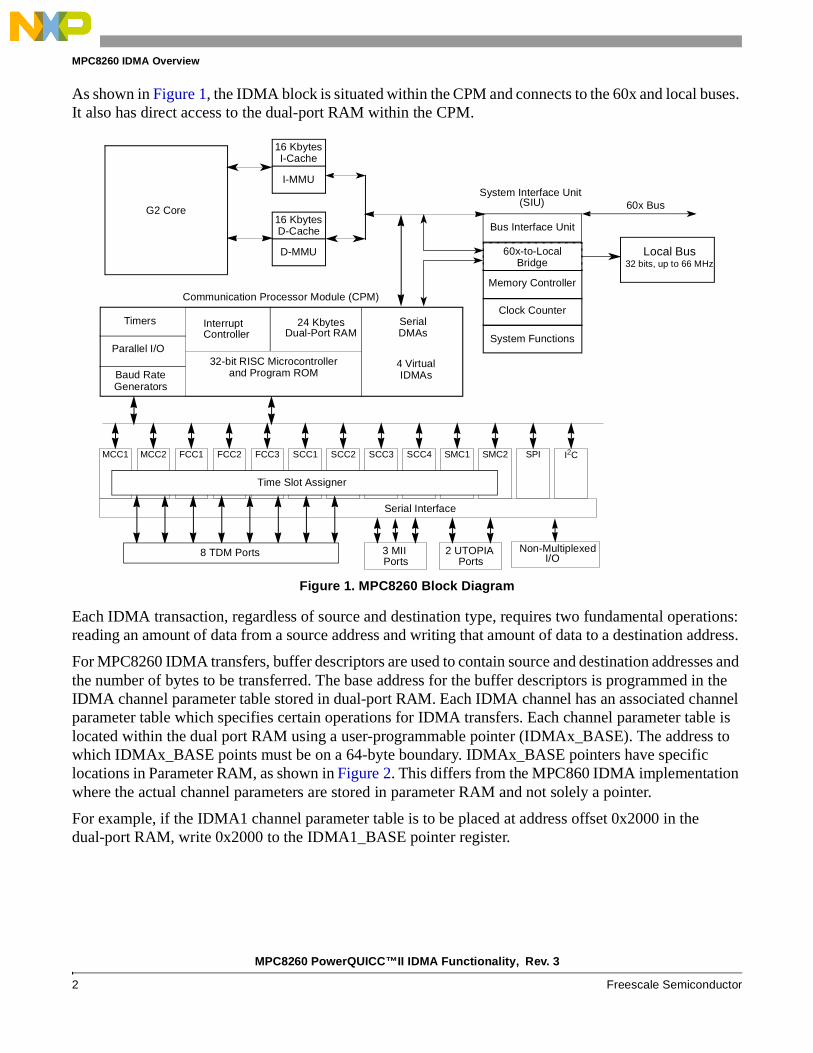
As shown in Figure 1, the IDMA block is situated within the CPM and connects to the 60x and local buses. It also has direct access to the dual-port RAM within the CPM.
Figure 1. MPC8260 Block Diagram
Each IDMA transaction, regardless of source and destination type, requires two fundamental operations: reading an amount of data from a source address and writing that amount of data to a destination address.
For MPC8260 IDMA transfers, buffer descriptors are used to contain source and destination addresses and the number of bytes to be transferred. The base address for the buffer descriptors is programmed in the IDMA channel parameter table stored in dual-port RAM. Each IDMA channel has an associated channel parameter table which specifies certain operations for IDMA transfers. Each channel parameter table is located within the dual port RAM using a user-programmable pointer (IDMAx_BASE). The address to which IDMAx_BASE points must be on a 64-byte boundary. IDMAx_BASE pointers have specific locations in Parameter RAM, as shown in Figure 2. This differs from the MPC860 IDMA implementation where the actual channel parameters are stored in parameter RAM and not solely a pointer.
For example, if the IDMA1 channel parameter table is to be placed at address offset 0x2000 in the dual-port RAM, write 0x2000 to the IDMA1_BASE pointer register.
16 Kbytes
G2 Core
I-Cache
I-MMU
16 KbytesD-Cache
D-MMU
Communication Processor Module (CPM)
Timers
Parallel I/O
Baud RateGenerators
24 Kbytes
32-bit RISC Microcontrollerand Program ROM
SerialDMAs
4 VirtualIDMAs
Bridge
Memory Controller
Clock Counter
System Functions
System Interface Unit (SIU)
Local Bus32 bits, up to 66 MHz
MCC1 MCC2 FCC1 FCC2 FCC3 SCC1 SCC2 SCC3 SCC4 SMC1 SMC2 SPI I2C
Serial Interface
3 MII 2 UTOPIA PortsPorts
60x Bus
Dual-Port RAMInterrupt Controller
Time Slot Assigner
8 TDM Ports Non-MultiplexedI/O
60x-to-Local
Bus Interface Unit

MPC8260 PowerQUICC™II IDMA Functionality, Rev. 3
Freescale Semiconductor 3
MPC8260 IDMA Overview
Figure 2. Memory Structure for IDMA Operation
IDMA transfers can be dual-address or single-address. Dual-address transfers use an intermediate transfer buffer stored in DPRAM. In single-address transfers (or fly-by mode), data is transferred without requiring an internal buffer. There are two modes that determine how an IDMA transaction is initiated:
• Internal request mode—The IDMA operates with the START_IDMA without the use of DREQ.
• External request mode—Every read transfer is triggered by the assertion of DREQ. When the transfer buffer is full, the first write transfer is carried out automatically. Additional write transfers are triggered by further DREQ assertions.
Memory-to-memory transfers are dual-address transfers. The IDMA first fills the transfer buffer in DPRAM with data read cycles from the source bus. Once the transfer buffer is full, data from the transfer buffer is transferred to the destination using write cycles. This is a dual-address transfer (single address mode is not valid for memory-to-memory transactions). The transfer sizes are programmed into IDMA parameter RAM. Memory-to-memory transfers can be achieved using internal and external request modes.
In peripheral-to-memory and memory-to-peripheral transfers, external signals DREQ, DACK and DONE are used to control data transfers. A read/write request from a peripheral is asserted via DREQ and is either rising-/falling-edge sensitive or level sensitive. The data is transferred/sampled when DACK is asserted. The peripheral asserts DONE to stop the transfer and terminates the current transfer when DONE and DACK are asserted (refer to Section 6, “IDMA Signals,” for more details).
Table 1. Valid IDMA transfers
Transfer TypeSingle Address
Internal RequestSingle Address
External RequestDual Address
Internal RequestDual Address
External Request
Memory-to-memory Invalid Invalid Valid Valid (DONE not supported)
Memory-to-peripheral Valid Valid Valid Valid
Peripheral-to-memory Valid Valid Invalid Valid
IDMA1_BASE0x87FE
IDMA1 ChannelParameter Table
IDMA2_BASE0x88FE
IDMA3_BASE0x89FE
IDMA4_BASE0x8AFE
Addressmust be 64 bytealigned
IDMA BufferDescriptors
External Memory
DestinationData
SourceData
Dual Port RAM 0x0000
Parameter RAM 0x8000
BD addressmust be 16 bit aligned
MPC8260 PowerQUICC™II IDMA Functionality, Rev. 3
4 Freescale Semiconductor
IDMA Software Initialization
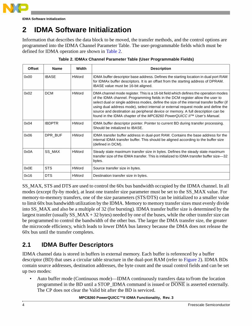
2 IDMA Software InitializationInformation that describes the data block to be moved, the transfer methods, and the control options are programmed into the IDMA Channel Parameter Table. The user-programmable fields which must be defined for IDMA operation are shown in Table 2.
SS_MAX, STS and DTS are used to control the 60x bus bandwidth occupied by the IDMA channel. In all modes (except fly-by mode), at least one transfer size parameter must be set to the SS_MAX value. For memory-to-memory transfers, one of the size parameters (STS/DTS) can be initialized to a smaller value to limit 60x bus bandwidth utilization by the IDMA. Memory to memory transfer sizes must evenly divide into SS_MAX and also be a multiple of 32 (for bursting). IDMA transfer buffer size is determined by the largest transfer (usually SS_MAX + 32 bytes) needed by one of the buses, while the other transfer size can be programmed to control the bandwidth of the other bus. The larger the DMA transfer size, the greater the microcode efficiency, which leads to lower DMA bus latency because the DMA does not release the 60x bus until the transfer completes.
2.1 IDMA Buffer DescriptorsIDMA channel data is stored in buffers in external memory. Each buffer is referenced by a buffer descriptor (BD) that uses a circular table structure in the dual-port RAM (refer to Figure 2). IDMA BDs contain source addresses, destination addresses, the byte count and the usual control fields and can be set up two modes:
• Auto buffer mode (Continuous mode)—IDMA continuously transfers data to/from the location programmed in the BD until a STOP_IDMA command is issued or DONE is asserted externally. The CP does not clear the Valid bit after the BD is serviced.
Table 2. IDMAx Channel Parameter Table (User Programmable Fields)
Offset Name Width Description
0x00 IBASE HWord IDMA buffer descriptor base address. Defines the starting location in dual port RAM for IDMAx buffer descriptors. It is an offset from the starting address of DPRAM. IBASE value must be 16-bit aligned.
0x02 DCM HWord DMA channel mode register. This is a 16-bit field which defines the operation modes of the IDMA channel. Programming fields in the DCM register allow the user to select dual or single address modes, define the size of the internal transfer buffer (if using dual address mode), select internal or external request mode and define the source and destination as peripheral device or memory. A full description can be found in the IDMA chapter of the MPC8260 PowerQUICC II™ User’s Manual.
0x04 IBDPTR HWord IDMA buffer descriptor pointer. Pointer to current BD during transfer processing. Should be initialized to IBASE.
0x06 DPR_BUF HWord IDMA transfer buffer address in dual-port RAM. Contains the base address for the internal IDMA transfer buffer. This should be aligned according to the buffer size (defined in DCM).
0x0A SS_MAX HWord Steady state maximum transfer size in bytes. Defines the steady state maximum transfer size of the IDMA transfer. This is initialized to IDMA transfer buffer size—32 bytes.
0x0E STS HWord Source transfer size in bytes.
0x16 DTS HWord Destination transfer size in bytes.
MPC8260 PowerQUICC™II IDMA Functionality, Rev. 3
Freescale Semiconductor 5
IDMA Software Initialization Example
• Buffer chaining mode—Data is transferred according to the first BD parameters, then the second BD and so on. The first BD is reused (if ready) until the BD with the last bit set is reached. IDMA transfers stop and restart when the BD table is reinitialized and a START_IDMA command is issued.
3 IDMA Software Initialization ExampleThese settings are for dual-address, memory-to-memory, internally requested transfers of 512 bytes from source address to destination address.
The maximum values of SS_MAX, STS and DTS are chosen to allow longer transfers and optimize bus usage. Therefore, a read from memory takes only one IDMA transfer to fill the internal buffer. The data is bursted into the internal buffer 32 bytes at a time. Once the internal buffer is full, it is emptied.
As determined by Table 18-7 in the MPC8260 PowerQUICC II™ User’s Manual, for 128 byte internal buffer, SS_MAX is 96 bytes, STS can be 96 or 32 bytes and DTS can be 96 or 32 bytes. For memory-to-memory transfers, if STS=DTS=SS_MAX, then one read transfer to fill the internal buffer is followed automatically by one write transfer to empty the internal buffer. This is done using burst cycles. Note that using a larger IDMA internal buffer and maximum transfer sizes (STS, DTS and SS_MAX) allows longer transfers, optimizes bus usage and reduces overall load on CP.
4 Setting IDMA PrioritiesThe IDMA block resides in the MPC8260 CPM. The communication processor (CP) within the CPM controls IDMA accesses, allowing the G2 core to carry out other activities. The priority which the CP services these IDMA requests is fixed (refer to Table 13.2, “Peripheral Prioritization,” in the MPC8260 PowerQUICC II™ User’s Manual). However, the IDMA priority can be programmed independently using the DREQx_B field in RCCR (RISC Controller Configuration Register refer to Section 13.3.6 in the MPC8260 PowerQUICC II™ User’s Manual). Each IDMA channel can be programmed to have a higher or lower priority relative to the other peripherals when it requests service from the CP.
When each IDMA channel has the same the priority setting in RCCR[DRxM], IDMA1 has highest priority and IDMA4 has lowest priority. The same priority level exists when the IDMA interrupts the G2 core.
Table 3. Initialization Example
Name Offset Description
IBASE 0x3800 IDMA BDs start at 0x04703800.
DCM 0x0040 Dual address; memory-to-memory; 128 byte internal transfer buffer; internal request mode
IBDPTR 0x3800 IDMA BD Pointer, initialized to IBASE value.
DPR_BUF 0x0800 IDMA internal transfer buffer at 0x0470800. This is aligned to internal buffer size (128 bytes).
SS_MAX 0x0060 Steady state value of 96 bytes. SS_MAX = internal buffer size -32 or (64 * 2 DMA_WRAP)-32.
STS 0x0060 Source transfer size of 96 bytes. This is maximum transfer size for internal buffer size used. Refer to Table 18-7 in the MPC8260 PowerQUICC II™ User’s Manual.
DTS 0x0060 Destination transfer size of 96 bytes. This is maximum transfer size for internal buffer size used. Refer to Table 18-7 in the MPC8260 PowerQUICC II™ User’s Manual.
MPC8260 PowerQUICC™II IDMA Functionality, Rev. 3
6 Freescale Semiconductor
IDMA Data Alignment
5 IDMA Data AlignmentAn efficient data-packing algorithm bursts data through the IDMA transfer buffer to minimize the bus cycles needed for the transfer. For the DMA to generate bursts on the 60x bus, the address boundaries of each burst transfer must be 32-byte aligned. If the transfer does not start on a burst boundary, the IDMA controller transfers the end-of-burst (EOB) data (1–31 bytes) in non-burst transactions on the source bus and destination bus until reaching the next boundary. When alignment is achieved, subsequent data is bursted until the remainder of the data in the buffer is less than a burst size (32 bytes). The remaining data is transferred using non-burst transactions. Unaligned data is transferred in single accesses until alignment is achieved. Then burst cycles are used to transfer the bulk of the data. Single accesses are again used to transfer any remaining data at the end of the transfer.
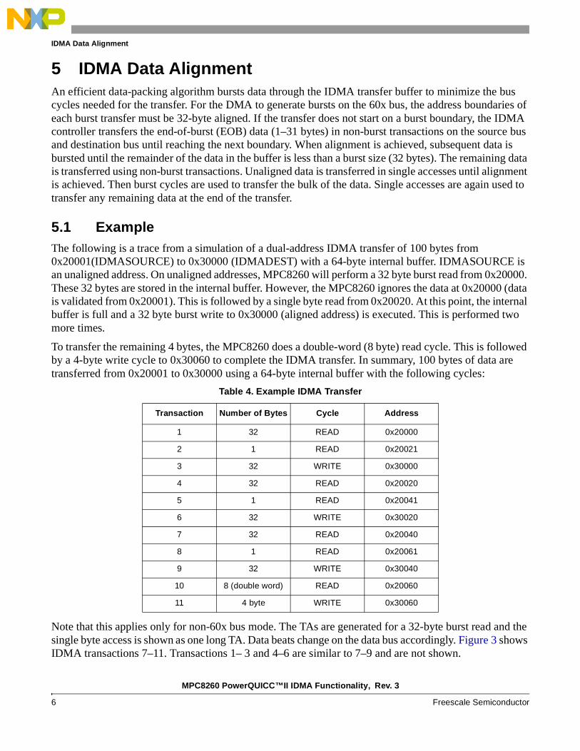
5.1 Example The following is a trace from a simulation of a dual-address IDMA transfer of 100 bytes from 0x20001(IDMASOURCE) to 0x30000 (IDMADEST) with a 64-byte internal buffer. IDMASOURCE is an unaligned address. On unaligned addresses, MPC8260 will perform a 32 byte burst read from 0x20000. These 32 bytes are stored in the internal buffer. However, the MPC8260 ignores the data at 0x20000 (data is validated from 0x20001). This is followed by a single byte read from 0x20020. At this point, the internal buffer is full and a 32 byte burst write to 0x30000 (aligned address) is executed. This is performed two more times.
To transfer the remaining 4 bytes, the MPC8260 does a double-word (8 byte) read cycle. This is followed by a 4-byte write cycle to 0x30060 to complete the IDMA transfer. In summary, 100 bytes of data are transferred from 0x20001 to 0x30000 using a 64-byte internal buffer with the following cycles:
Note that this applies only for non-60x bus mode. The TAs are generated for a 32-byte burst read and the single byte access is shown as one long TA. Data beats change on the data bus accordingly. Figure 3 shows IDMA transactions 7–11. Transactions 1– 3 and 4–6 are similar to 7–9 and are not shown.
Table 4. Example IDMA Transfer
Transaction Number of Bytes Cycle Address
1 32 READ 0x20000
2 1 READ 0x20021
3 32 WRITE 0x30000
4 32 READ 0x20020
5 1 READ 0x20041
6 32 WRITE 0x30020
7 32 READ 0x20040
8 1 READ 0x20061
9 32 WRITE 0x30040
10 8 (double word) READ 0x20060
11 4 byte WRITE 0x30060

MPC8260 PowerQUICC™II IDMA Functionality, Rev. 3
Freescale Semiconductor 7
IDMA Data Alignment
Figure 3. Single Bus Mode IDMA Transfer (Memory-to-Memory)
8
7
911
10
pp
c_a[
0:31
]ab
bd
[0:6
3]b
ank
sele
ct0
ban
kse
lect
1b
ank
sele
ct2
sdra
s
sdca
ssd
we
sda1
0 tsaa
ck tats
ize[
0:3]
tt[0
:4]
tbst
cs[0
:9]
dq
m[0
:7]
MPC8260 PowerQUICC™II IDMA Functionality, Rev. 3
8 Freescale Semiconductor
IDMA Signals
6 IDMA SignalsEach IDMA channel has three signals that are used for peripheral handshaking. The signals are multiplexed at the parallel I/O port pins.
7 Technical Description of SoftwareThis example code transfers 512 bytes of data (IDMASIZE_BYTES) from a source buffer (IDMASOURCE) to an destination buffer (DST_ADDR_LOCAL) using an internal IDMA transfer buffer of 128 bytes. The code uses IDMA2 to implement memory-to-memory transfers, in this case 60x bus SDRAM to local-bus SDRAM. The user determines the number of buffer descriptors used with the NO_OF_BDs variable declared in the IDMATEST.h file. The code contains a checkbuf() function which ensures the transfer has been successful by making sure the destination buffer matches the source buffer. If the transfer has been successful the green LED (LD11) will be illuminated. If the buffers do not match, the red LED (LD12) is illuminated.
Table 5. IDMA Signals
Signal Description
DREQ DMA request. Peripheral asserts DREQ when it needs services. DREQ is sampled at the rising edge of clock and can be configured as edge or level sensitive. DREQ may also be used to control the transfer pace of Memory-to-Memory transfers
DACK DMA Acknowledge. When the IDMA service is in progress, the MPC8260 asserts DACK during accesses to the peripheral. The peripheral must validate the transfer by asserting TA or TEA. DACK is the acknowledgment of the original request for DMA transactions.
DONE Indicates last IDMA transfer. DONE can be an output if a previously set up transfer count is exhausted, or used as an input to the IDMA controller to indicate that a peripheral being serviced requires no more IDMA transactions.
Table 6. Memory/Peripheral IDMA Signals
Address Type STS DTS Explanation
Dual Peripheral-to-memory Port size or 32
SS_MAX Peripheral assert DREQ.
MPC8260 asserts DACK.
Data transferred to internal buffer in STS bytes.
When internal buffer contains SS_MAX, buffer is emptied in SS_MAX bytes.
Dual Memory -to -peripheral SS_MAX Port Size or 32
Peripheral assert DREQ. MPC8260 responds with DACK
SS_MAX bytes are transferred from memory to internal buffer followed by a write of DTS bytes.
Further DREQs initiate further writes of DTS bytes.
If internal buffer contains < DTS bytes, next DREQ initiates read of SS_MAX bytes, sequence repeats.
Single Peripheral -to -memory Port size — Peripheral asserts DREQ. MPC8260 responds with DACK at the same time as writing to memory.
Single Memory-to -peripheral — Port Size Peripheral asserts DREQ. MPC8260 responds with DACK at the same time as reading from memory.
MPC8260 PowerQUICC™II IDMA Functionality, Rev. 3
Freescale Semiconductor 9
Technical Description of Software
The sources are as follows:
• idma_int.c—IDMA2 channel is set up in internal request mode, that is once the IDMA START command is issued, IDMA transactions are started immediately. The IDMA will be complete when all associated buffer descriptors have been closed.
• idma_ext.c—IDMA2 channel is set up in external request mode, that is the IDMA transfer is performed only when DREQ2 has been asserted. Each IDMA2 transaction needs a DREQ2 signal, the general purpose I/O pin, PC[30], is being used for this purpose. A physical connection from PC[30] to DREQ2 must be made on the MPC8260VADS board. This is achieved through the CPM expansion connector, P4. PC[30] is D2 and DREQ[2]/PC[1] is D31 on this connector.
In both cases, if the IDMA transfer is successful, the source data is transferred to the destination address. The source buffer contains 32 bytes of 0’s, followed by 32 bytes of 1’s, and so on up to 32 bytes of F’s.
7.1 Recommended Programming Sequence1. Establish a pointer to MPC8260 internal memory map.
2. Establish a pointer to IDMA buffer descriptors.
3. Clear the MPC8260 dual-port RAM.
4. Clear destination memory (in this case 0x04000000).
5. Set up interrupt handler code. Copy the code to the specified PowerPC interrupt vector (0x500).
6. Program source memory with IDMASIZE_BYTES (in this case 0x00020001).
7. Initialize IDMA buffer descriptors. No_of_BDS in idmatest.h determines the number of buffer descriptors used.
8. Initialize IDMA. For this example, dual address transfers, 128 bytes IDMA transfer buffer, memory to memory, internal or external request mode, transfers and steady state values.
9. Set up ports for DREQ2. Initialize ports and set PC[1] as DREQ2. (idma_ext.c only).
10. Initialize interrupt controller. Set up interrupts for IDMA2 and enable external interrupts.
11. Set up ports for input to DREQ2. For this example, PC[30] is used as an input to DREQ2. (idma_ext.c only).
12. Issue IDMA START command by writing to CPCR register.
13. Check transfer was successful. Compare source and destination buffers.
7.2 Using This ProgramThis code is designed to run on an MPC8260ADS board. It does not initialize the PowerPC core. Useful addresses for this example include the following:
• 0x00020001—Source data buffer
• 0x04000000—Destination data buffer
• 0x04700000—IDMA buffer descriptors
• 0x04700800— IDMA Internal transfer buffer
• 0x04703800—IDMA channel parameters
MPC8260 PowerQUICC™II IDMA Functionality, Rev. 3
10 Freescale Semiconductor
Technical Description of Software
7.3 Modifying the SoftwareWhen modifying the software for other applications, note the following:
• Always consult the latest version of the MPC8260 device errata (see Section 8, “References”).
• If the software is changed to use IDMA 1, 3 or 4, it should be noted that the RCCR contains a DRxM bit for each IDMA and will need to be modified to ensure that the DREQx is level sensitive.
• Care should be taken when modifying the port settings. The programming of a DREQ pin generates a transition on the internal DREQ signals. This may cause an IDMA transaction, and if the IDMA is not initialized at that time the CPM may lock. To prevent this the example software holds the input to DREQ (PC30) low until after the DREQ pin has been programmed.
7.4 File StructureThe following files are included:
1. idma_int.c—Main source file for internal request mode example.
2. idma_ext.c—Main source file for external request mode example.
3. idmatest.h—Main header file.
4. startup.s—The assembly file that contains definitions for the stack frame and interrupt structures. Can also contain the initialization code when using other development systems.
5. masks8260.h—This header file contains standard masks used to develop MPC8260 software.
6. mpc8260.h—This header file contains the Internal Memory Map (IMM) structure declarations for the MPC8260.
7. netcomm.h—This header file contains global data type definitions.
8. idma_int.map & idma_ext.map—Compiler Generated address map files.
9. comp.bat—DOS batch file for compilation and linking. To compile a file, at DOS prompt type comp idma_int.
10. idma_int.elf & idma_ext.elf—Downloadable ELF files.
11. idma.lnx—Compiler Generated mixed source and assembler file.
12. startup.L—Compiler Generated mixed source and assembler file.
7.5 Development EnvironmentThe following development tools were used:
• DIAB 4.3f C/C++ Compiler, Assembler and Linker
• SDS Singlestep 7.5 Debugger
• MPC8260 ADS development board (PILOT version)
• Windows 2000 platform
The DIAB toolset was used to produce an ELF file that was downloaded using the SDS Singlestep Debugger. This software was only tested and compiled on a Windows 2000 platform.
MPC8260 PowerQUICC™II IDMA Functionality, Rev. 3
Freescale Semiconductor 11
References
The development tools mentioned here are not an expressed or implied endorsement, and does not communicate preference of one manufacturer’s product over another. We simply chose to use these particular manufacturer’s products in this example.
7.6 TestingAll tests were conducted using SDS SingleStep software debugger environment Version 7.5 and a Macraigor RAVEN probe. The memory map values, buffer descriptor set-up, and source and destination buffers in external memory were all verified with SDS Singlestep 7.5 debugging suite.
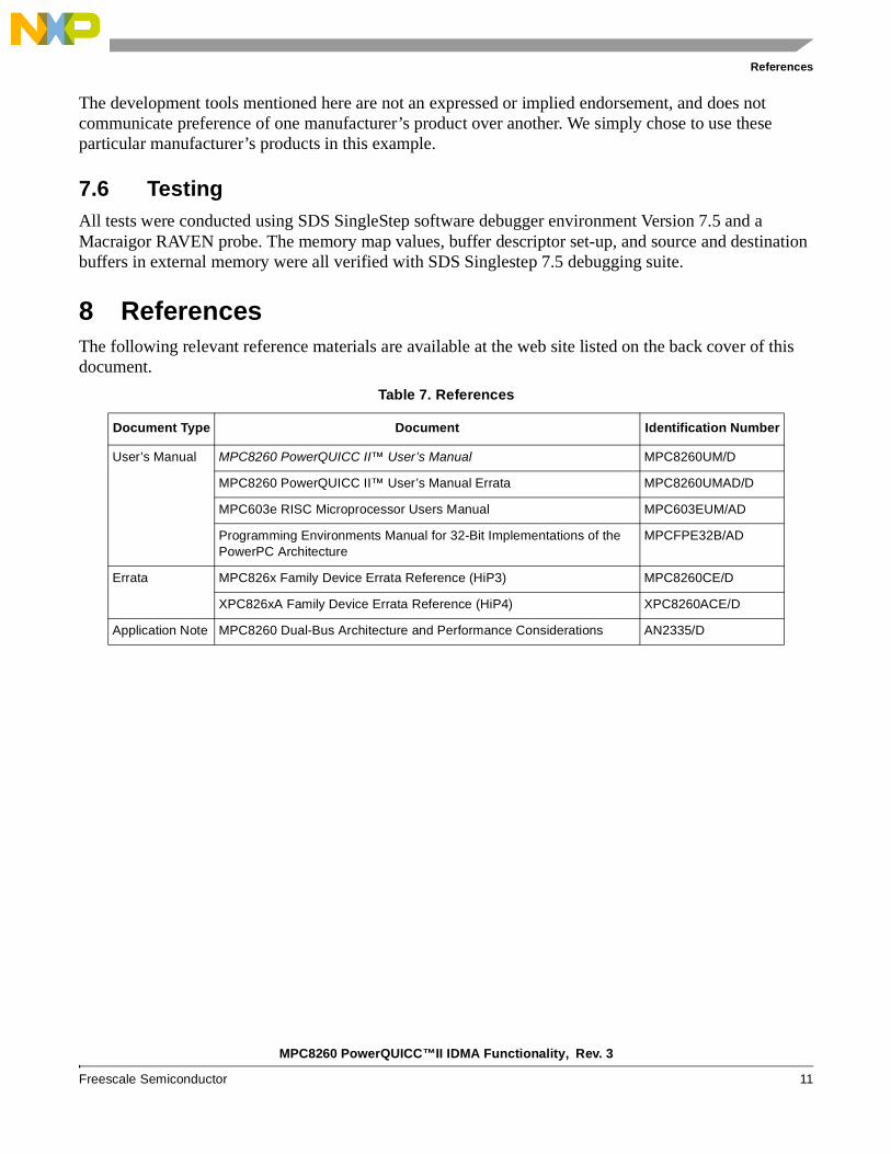
8 ReferencesThe following relevant reference materials are available at the web site listed on the back cover of this document.
Table 7. References
Document Type Document Identification Number
User’s Manual MPC8260 PowerQUICC II™ User’s Manual MPC8260UM/D
MPC8260 PowerQUICC II™ User’s Manual Errata MPC8260UMAD/D
MPC603e RISC Microprocessor Users Manual MPC603EUM/AD
Programming Environments Manual for 32-Bit Implementations of the PowerPC Architecture
MPCFPE32B/AD
Errata MPC826x Family Device Errata Reference (HiP3) MPC8260CE/D
XPC826xA Family Device Errata Reference (HiP4) XPC8260ACE/D
Application Note MPC8260 Dual-Bus Architecture and Performance Considerations AN2335/D
Document Number: AN2430Rev. 302/2006
Freescale™ and the Freescale logo are trademarks of Freescale Semiconductor, Inc. All other product or service names are the property of their respective owners.
© Freescale Semiconductor, Inc., 2002, 2006.
Information in this document is provided solely to enable system and software
implementers to use Freescale Semiconductor products. There are no express or
implied copyright licenses granted hereunder to design or fabricate any integrated
circuits or integrated circuits based on the information in this document.
Freescale Semiconductor reserves the right to make changes without further notice to
any products herein. Freescale Semiconductor makes no warranty, representation or
guarantee regarding the suitability of its products for any particular purpose, nor does
Freescale Semiconductor assume any liability arising out of the application or use of
any product or circuit, and specifically disclaims any and all liability, including without
limitation consequential or incidental damages. “Typical” parameters which may be
provided in Freescale Semiconductor data sheets and/or specifications can and do
vary in different applications and actual performance may vary over time. All operating
parameters, including “Typicals” must be validated for each customer application by
customer’s technical experts. Freescale Semiconductor does not convey any license
under its patent rights nor the rights of others. Freescale Semiconductor products are
not designed, intended, or authorized for use as components in systems intended for
surgical implant into the body, or other applications intended to support or sustain life,
or for any other application in which the failure of the Freescale Semiconductor product
could create a situation where personal injury or death may occur. Should Buyer
purchase or use Freescale Semiconductor products for any such unintended or
unauthorized application, Buyer shall indemnify and hold Freescale Semiconductor
and its officers, employees, subsidiaries, affiliates, and distributors harmless against all
claims, costs, damages, and expenses, and reasonable attorney fees arising out of,
directly or indirectly, any claim of personal injury or death associated with such
unintended or unauthorized use, even if such claim alleges that Freescale
Semiconductor was negligent regarding the design or manufacture of the part.
How to Reach Us:
Home Page: www.freescale.com
email: [email protected]
USA/Europe or Locations Not Listed: Freescale Semiconductor Technical Information Center, CH3701300 N. Alma School Road Chandler, Arizona 85224 [email protected]
Europe, Middle East, and Africa:Freescale Halbleiter Deutschland GmbHTechnical Information CenterSchatzbogen 781829 Muenchen, Germany+44 1296 380 456 (English) +46 8 52200080 (English)+49 89 92103 559 (German)+33 1 69 35 48 48 (French) [email protected]
Japan: Freescale Semiconductor Japan Ltd. HeadquartersARCO Tower 15F1-8-1, Shimo-Meguro, Meguro-ku Tokyo 153-0064, Japan 0120 191014+81 3 5437 [email protected]
Asia/Pacific: Freescale Semiconductor Hong Kong Ltd. Technical Information Center2 Dai King Street Tai Po Industrial Estate, Tai Po, N.T., Hong Kong +800 2666 [email protected]
For Literature Requests Only:Freescale Semiconductor
Literature Distribution Center P.O. Box 5405Denver, Colorado 80217 1-800-441-2447303-675-2140Fax: 303-675-2150LDCForFreescaleSemiconductor
@hibbertgroup.com