mp6517 programmable single-phase, bldc, motor driver with
TRANSCRIPT

MP6517 Programmable Single-Phase, BLDC, Motor Driver with Integrated
Hall Sensor
MP6517 Rev.1.01 www.MonolithicPower.com 1 4/9/2018 MPS Proprietary Information. Patent Protected. Unauthorized Photocopy and Duplication Prohibited. © 2018 MPS. All Rights Reserved.
The Future of Analog IC Technology
DESCRIPTION The MP6517 is a single-phase, brushless, DC motor driver with integrated power MOSFETs and a Hall effect sensor. The MP6517 drives single-phase, brushless, DC fan motors with up to 1.2A of output current limit. The IC has a 3.3V to 18V input voltage range and input line reverse voltage protection to save the external diode on the supply line.
The MP6517 controls the rotational speed through the PWM signal on the PWM pin. The MP6517 has a rotational speed detector feature and rotor lock fault indication on FG/RD with an open-drain collector output. The output speed versus the input duty curve can be programmed easily for flexible use. To reduce fan driver audible noise and power loss, the MP6517 features a soft on/off phase transition and automatic phase-lock function of the motor winding BEMF and current.
Full protection features include input over-voltage protection (OVP), under-voltage lockout (UVLO), rotor deadlocked protection, thermal shutdown, and input reverse protection.
The MP6517 requires a minimal number of external components to save solution cost. The MP6517 is available in a TSOT23-6 package.
FEATURES Embedded Hall Sensor with High Sensitivity Wide 3.3V to 18V Operating Input Range Up to 1.2A Programmable Current Limit Integrated Power MOSFETs: Total 850mΩ
(HS + LS) Programmable Speed Curve Automatic Phase Lock Detection of Winding
BEMF and Current Zero-Crossing Soft On/Off Phase Transition Rotational Speed Indicator FG Signal 12kHz to 48kHz PWM Input Frequency
Range Fixed 26kHz Output Switching Frequency Input Line Reverse Voltage Protection (RVP) Rotor Deadlocked Protection and Automatic
Recovery Thermal Protection and Automatic Recovery Built-In Input OVP, UVLO, and Automatic
Recovery Available in a TSOT23-6 Package
APPLICATIONS CPU Fan for Personal Computers or
Servers Brushless DC Motors
All MPS parts are lead-free, halogen-free, and adhere to the RoHS directive. ForMPS green status, please visit the MPS website under Quality Assurance. “MPS” and “The Future of Analog IC Technology” are registered trademarks of Monolithic Power Systems, Inc.
TYPICAL APPLICATION

MP6517 – SINGLE-PHASE, BLDC, MOTOR DRIVER WITH INTEGRATED HALL SENSOR
MP6517 Rev.1.01 www.MonolithicPower.com 2 4/9/2018 MPS Proprietary Information. Patent Protected. Unauthorized Photocopy and Duplication Prohibited. © 2018 MPS. All Rights Reserved.
ORDERING INFORMATION Part Number * Package Top Marking
MP6517GJ-xxxx ** TSOT23-6 See Below
MP6517GJS-xxxx ** TSOT23-6-SL
* For Tape & Reel, add suffix –Z (e.g. MP MP6517GJS–Z). ** “xxxx” is the configuration code identifier for the register settings stored in the OTPROM. For the default case,
the number is “0000”. Each “x” can have a hexadecimal value between 0 and F. Please work with an MPS FAE to create this unique number, even if ordering the “0000” code.
TOP MARKING (MP6517GJ)
ATA: Product code of MP6517GJ Y: Year code
TOP MARKING (MP6517GJS)
ATA: Product code of MP6517GJS Y: Year code LLL: Lot number

MP6517 – SINGLE-PHASE, BLDC, MOTOR DRIVER WITH INTEGRATED HALL SENSOR
MP6517 Rev.1.01 www.MonolithicPower.com 3 4/9/2018 MPS Proprietary Information. Patent Protected. Unauthorized Photocopy and Duplication Prohibited. © 2018 MPS. All Rights Reserved.
PACKAGE REFERENCE
TOP VIEW
TSOT23-6 TSOT23-6-SL
ABSOLUTE MAXIMUM RATINGS (1) VCC ........................................................... ±19V FG/RD, VOUT1/2 ................... -0.3V to VCC + 0.3V All other pins ................................ -0.3V to +6.5V
Continuous power dissipation (TA = +25°C) (2)
................................................................. 1.25W Junction temperature ................................ 150°C Lead temperature ..................................... 260°C Storage temperature .................. -60°C to 150°C
Recommended Operating Conditions (3) Supply voltage (VCC) ...................... 3.3V to 18V Operating junction temp. (TJ) ... -40°C to +125°C
Thermal Resistance (4) θJA θJC TSOT23-6 ............................. 100 ...... 55 ... °C/W
NOTES: 1) Exceeding these ratings may damage the device. 2) The maximum allowable power dissipation is a function of the
maximum junction temperature TJ (MAX), the junction-to-ambient thermal resistance θJA, and the ambient temperature TA. The maximum allowable continuous power dissipation at any ambient temperature is calculated by PD (MAX) = (TJ
(MAX)-TA)/θJA. Exceeding the maximum allowable power dissipation produces an excessive die temperature, causing the regulator to go into thermal shutdown. Internal thermal shutdown circuitry protects the device from permanent damage.
3) The device is not guaranteed to function outside of its operating conditions.
4) Measured on JESD51-7, 4-layer PCB.
MP6517 – SINGLE-PHASE, BLDC, MOTOR DRIVER WITH INTEGRATED HALL SENSOR
MP6517 Rev.1.01 www.MonolithicPower.com 4 4/9/2018 MPS Proprietary Information. Patent Protected. Unauthorized Photocopy and Duplication Prohibited. © 2018 MPS. All Rights Reserved.
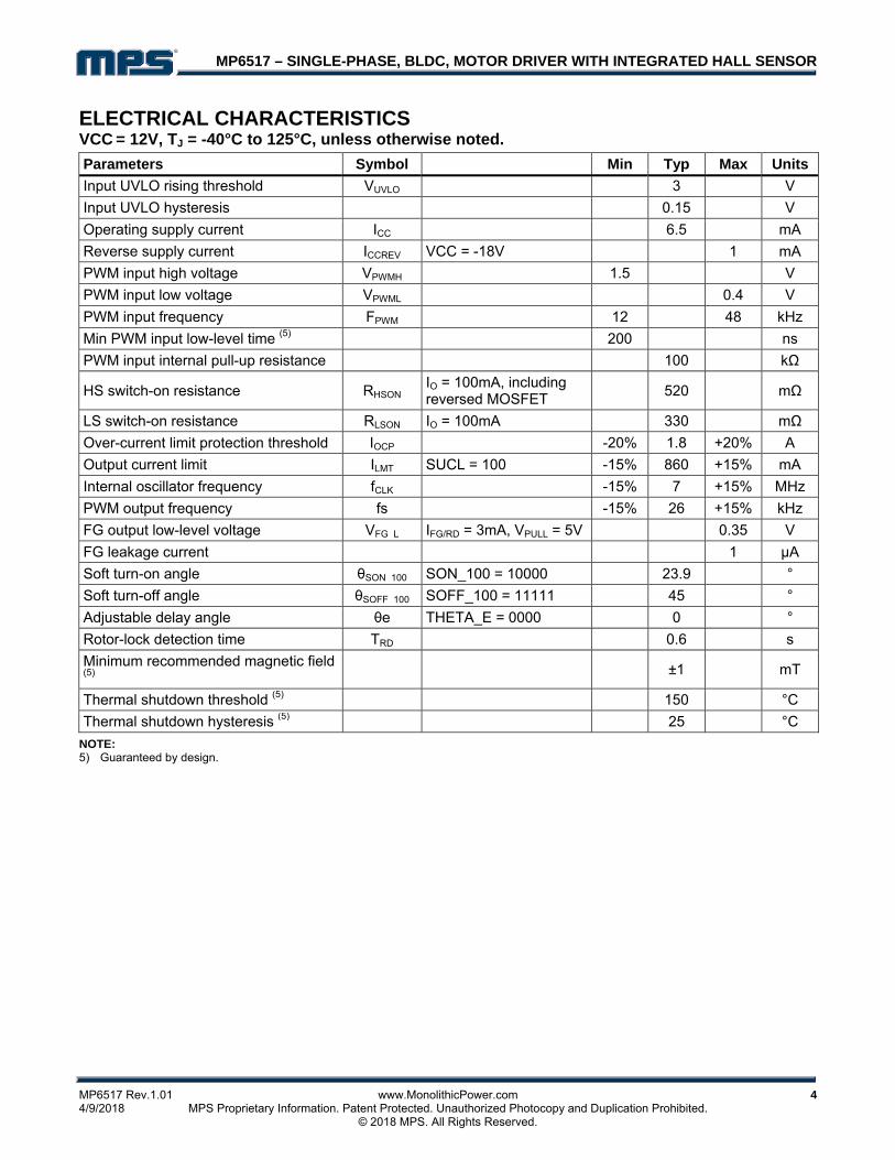
ELECTRICAL CHARACTERISTICS VCC = 12V, TJ = -40°C to 125°C, unless otherwise noted.
Parameters Symbol Min Typ Max Units
Input UVLO rising threshold VUVLO 3 V
Input UVLO hysteresis 0.15 V
Operating supply current ICC 6.5 mA
Reverse supply current ICCREV VCC = -18V 1 mA
PWM input high voltage VPWMH 1.5 V
PWM input low voltage VPWML 0.4 V
PWM input frequency FPWM 12 48 kHz
Min PWM input low-level time (5) 200 ns
PWM input internal pull-up resistance 100 kΩ
HS switch-on resistance RHSON IO = 100mA, including reversed MOSFET
520 mΩ
LS switch-on resistance RLSON IO = 100mA 330 mΩ
Over-current limit protection threshold IOCP -20% 1.8 +20% A
Output current limit ILMT SUCL = 100 -15% 860 +15% mA
Internal oscillator frequency fCLK -15% 7 +15% MHz
PWM output frequency fs -15% 26 +15% kHz
FG output low-level voltage VFG L IFG/RD = 3mA, VPULL = 5V 0.35 V
FG leakage current 1 µA
Soft turn-on angle θSON 100 SON_100 = 10000 23.9 °
Soft turn-off angle θSOFF 100 SOFF_100 = 11111 45 °
Adjustable delay angle θe THETA_E = 0000 0 °
Rotor-lock detection time TRD 0.6 s
Minimum recommended magnetic field (5)
±1 mT
Thermal shutdown threshold (5) 150 °C
Thermal shutdown hysteresis (5) 25 °C
NOTE: 5) Guaranteed by design.
MP6517 – SINGLE-PHASE, BLDC, MOTOR DRIVER WITH INTEGRATED HALL SENSOR
MP6517 Rev.1.01 www.MonolithicPower.com 5 4/9/2018 MPS Proprietary Information. Patent Protected. Unauthorized Photocopy and Duplication Prohibited. © 2018 MPS. All Rights Reserved.
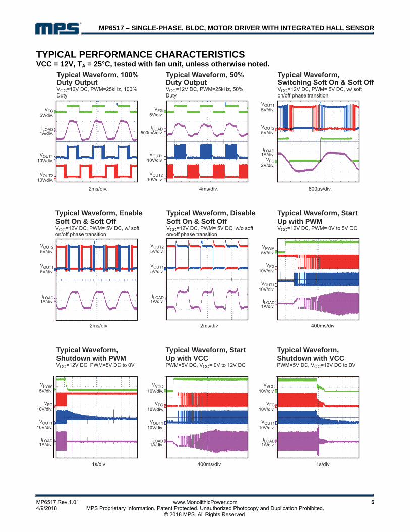
TYPICAL PERFORMANCE CHARACTERISTICS VCC = 12V, TA = 25°C, tested with fan unit, unless otherwise noted.
Typical Waveform, Enable Soft On & Soft Off VCC=12V DC, PWM= 5V DC, w/ soft on/off phase transition
Typical Waveform, Disable Soft On & Soft Off VCC=12V DC, PWM= 5V DC, w/o soft on/off phase transition
Typical Waveform, Shutdown with PWMVCC=12V DC, PWM=5V DC to 0V
Typical Waveform, Start Up with PWMVCC=12V DC, PWM= 0V to 5V DC
Typical Waveform, Shutdown with VCCPWM=5V DC, VCC=12V DC to 0V
Typical Waveform, Start Up with VCCPWM=5V DC, VCC= 0V to 12V DC
VOUT110V/div.
VFG5V/div.
VOUT210V/div.
VOUT25V/div.
VOUT15V/div.
ILOAD1A/div.
ILOAD1A/div.
VOUT25V/div.
VOUT15V/div.
ILOAD1A/div.
VPWM5V/div.
VOUT110V/div.
ILOAD1A/div.
VOUT110V/div.
VFG5V/div.
VFG10V/div.
VPWM5V/div.
VOUT110V/div.
ILOAD1A/div.
VFG10V/div.
VVCC10V/div.
VOUT110V/div.
ILOAD1A/div.
VFG10V/div.
VVCC10V/div.
VOUT110V/div.
ILOAD1A/div.
VFG10V/div.
VOUT210V/div.
ILOAD500mA/div.
VOUT15V/div.
VFG2V/div.
VOUT25V/div.
ILOAD1A/div.
MP6517 – SINGLE-PHASE, BLDC, MOTOR DRIVER WITH INTEGRATED HALL SENSOR
MP6517 Rev.1.01 www.MonolithicPower.com 6 4/9/2018 MPS Proprietary Information. Patent Protected. Unauthorized Photocopy and Duplication Prohibited. © 2018 MPS. All Rights Reserved.
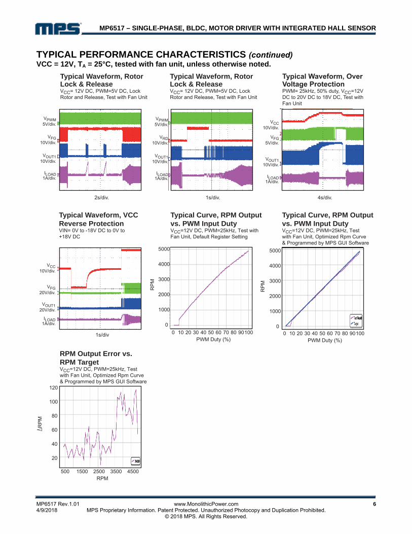
TYPICAL PERFORMANCE CHARACTERISTICS (continued) VCC = 12V, TA = 25°C, tested with fan unit, unless otherwise noted.
RP
M
Typical Waveform, VCC Reverse ProtectionVIN= 0V to -18V DC to 0V to +18V DC
Typical Curve, RPM Output vs. PWM Input DutyVCC=12V DC, PWM=25kHz, Test with Fan Unit, Default Register Setting
RPM Output Error vs. RPM TargetVCC=12V DC, PWM=25kHz, Test with Fan Unit, Optimized Rpm Curve & Programmed by MPS GUI Software
Typical Curve, RPM Output vs. PWM Input DutyVCC=12V DC, PWM=25kHz, Test with Fan Unit, Optimized Rpm Curve & Programmed by MPS GUI Software
Typical Waveform, Rotor Lock & ReleaseVCC= 12V DC, PWM=5V DC, Lock Rotor and Release, Test with Fan Unit
Typical Waveform, Rotor Lock & ReleaseVCC= 12V DC, PWM=5V DC, Lock Rotor and Release, Test with Fan Unit
VPWM5V/div.
VOUT110V/div.
ILOAD1A/div.
VFG10V/div.
VPWM5V/div.
VOUT110V/div.
ILOAD1A/div.
VRD10V/div.
VCC10V/div.
VOUT110V/div.
ILOAD1A/div.
VFG5V/div.
VCC10V/div.
VOUT120V/div.
ILOAD1A/div.
VFG20V/div.
5000
4000
3000
2000
1000
0
RP
M
100
120
80
60
40
20
RP
M
5000
4000
3000
2000
1000
00 10 20 30 40 50 60 70 80 90100
RPM500 1500 2500 3500 4500
0 10 20 30 40 50 60 70 80 90100

MP6517 – SINGLE-PHASE, BLDC, MOTOR DRIVER WITH INTEGRATED HALL SENSOR
MP6517 Rev.1.01 www.MonolithicPower.com 7 4/9/2018 MPS Proprietary Information. Patent Protected. Unauthorized Photocopy and Duplication Prohibited. © 2018 MPS. All Rights Reserved.
PIN FUNCTIONS Pin # Name Description
1 GND Ground.
2 VCC Input voltage supply.
3 FG/RD/SCL Speed indication or rotor lock fault indication output. This pin functions as I2C SCL intest mode (TM).
4 PWM/SDA Rotational speed control PWM input. PWM 12kHz to 48kHz is recommended in normal operation. PWM is an internal pull-up with 100kΩ of resistance to the internal LDO. This pin functions as I2C SDA in test mode (TM).
5 OUT2 Motor driver output 2. OUT2 is connected to the mid-point of the internal N-channel MOSFET half-bridge.
6 OUT1 Motor driver output 1. OUT1 is connected to the mid-point of the internal N-channel MOSFET half-bridge.
MP6517 – SINGLE-PHASE, BLDC, MOTOR DRIVER WITH INTEGRATED HALL SENSOR
MP6517 Rev.1.01 www.MonolithicPower.com 8 4/9/2018 MPS Proprietary Information. Patent Protected. Unauthorized Photocopy and Duplication Prohibited. © 2018 MPS. All Rights Reserved.
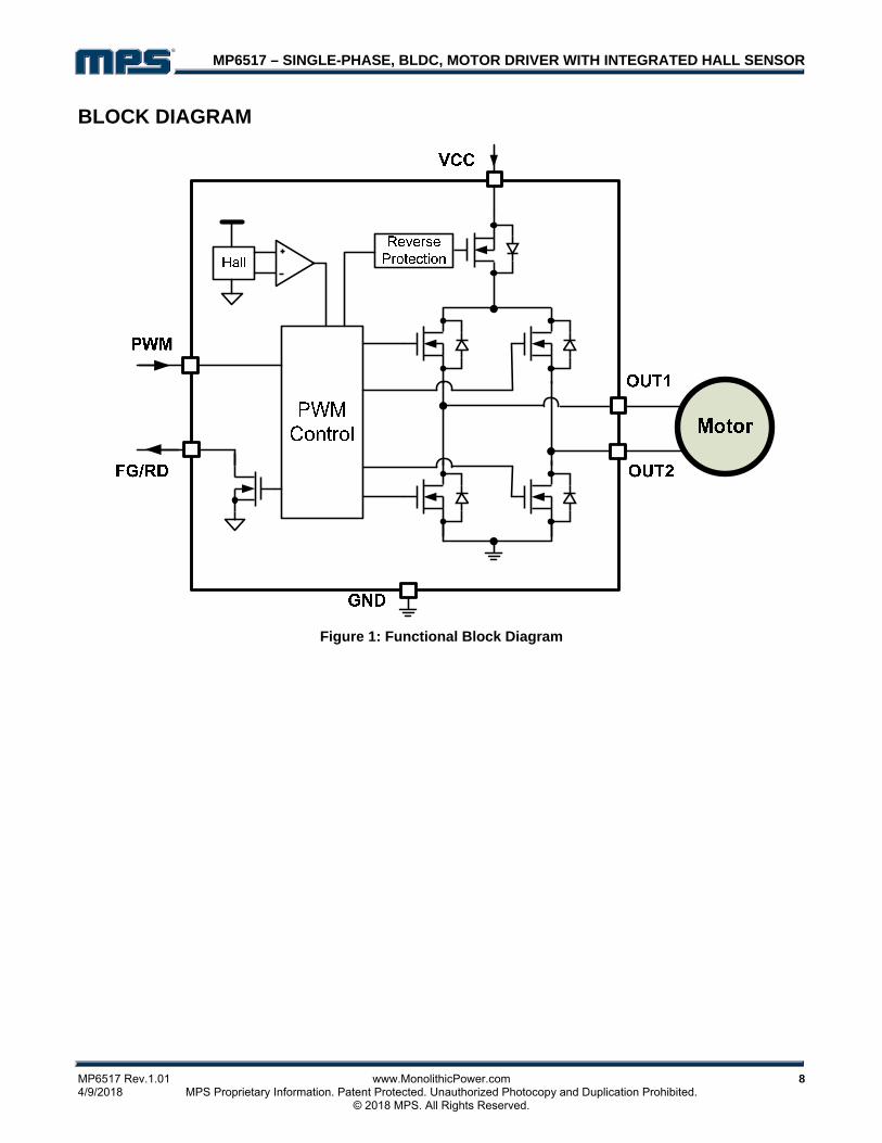
BLOCK DIAGRAM
Figure 1: Functional Block Diagram

MP6517 – SINGLE-PHASE, BLDC, MOTOR DRIVER WITH INTEGRATED HALL SENSOR
MP6517 Rev.1.01 www.MonolithicPower.com 9 4/9/2018 MPS Proprietary Information. Patent Protected. Unauthorized Photocopy and Duplication Prohibited. © 2018 MPS. All Rights Reserved.
OPERATION The MP6517 is a single-phase, brushless, DC motor driver with integrated power MOSFETs and a Hall effect sensor.
Speed Control
The MP6517 is controlled using a PWM input interface, which is compatible with industry-standard devices. The IC detects the PWM input signal duty cycle and linearly controls the H-bridge output duty cycle, so the fan speed increases as the input duty cycle increases.
The PWM input accepts a wide input frequency range (12kHz to 48kHz), while the output frequency is kept constant at 26kHz above the audible frequency range.
PWM Output Drive
The IC controls the H-bridge MOSFET switching to reduce speed variation and increase system efficiency (see Figure 2).
When the rotor magnet pole S comes around, the internal Hall sensor outputs high. When the rotor magnet pole N comes around, the internal Hall sensor outputs low. With this HA_IN signal, the HA_OUT signal is generated after the θe delay time, which is set from 0° to 15° through the register THETA_E bits. During the HA_OUT high interval, the OUT2 and OUT1 switching status can be divided to different timing sections.
Figure 2: Timing Diagram
Soft Turn-On Section
During this time, OUT1 continues switching, and the duty cycle increases gradually from 0 to the target setting duty cycle in 16 steps max. OUT2 remains low. Determine the duration time from the linear interpolation between the
SON_100 and SON_12P5 bits setting value, which is in range of 1.45° to 45° in 32 steps.
Normal PWM Switching Section
During this time, OUT1 continues switching, and the duty cycle is fixed at the target setting duty. OUT2 remains low.
Soft Turn-Off Section
During this time, OUT1 continues switching, and the duty cycle decreases gradually from the target setting duty cycle to 0 in 16 steps max. OUT2 remains low. Determine the duration time from the linear interpolation between the SOFF_100 and SOFF_12P5 bits setting value, which is in range of 1.45° to 45° in 32 steps.
Off Section
During this time, OUT1 remains at high impedance. OUT2 remains low. The time duration is adaptive from 0° to 45°. In steady state, this function block tries to maintain the phase lock of the Hall output falling edge and winding current zero-crossing edge.
For Hall output low interval, the conducting phase changes, but the switching sequence remains the same.
Protection Circuits
The MP6517 is fully protected against over-voltage, under-voltage, over-current, over-temperature events, and input reverse protection.
Over-Current Protection (OCP)
The MP6517 protects against internal overload and short circuit by detecting the current flowing through each MOSFET. If the current flowing through any MOSFET exceeds the over-current protection (OCP) threshold after around 1.5µs of blanking time, that MOSFET turns off immediately. After approximately 3.6s of delay, the bridge is re-enabled automatically.
Overload Current Limit
During normal switching, if the current flowing through the high-side MOSFET (HS-FET) of the H-bridge exceeds the threshold set by the register SUCL bits after around 1.5µs of blanking time, the HS-FET turns off immediately. The HS-FET resumes switching in the next switching cycle. The overload current limit is fixed at around 860mA. To spin-up the fan

MP6517 – SINGLE-PHASE, BLDC, MOTOR DRIVER WITH INTEGRATED HALL SENSOR
MP6517 Rev.1.01 www.MonolithicPower.com 10 4/9/2018 MPS Proprietary Information. Patent Protected. Unauthorized Photocopy and Duplication Prohibited. © 2018 MPS. All Rights Reserved.
driver softly during start-up, the current limit increases from 0 to the programmed current limit in 16 steps (see Figure 3). Each step limit value lasts for 16 internal Hall cycles. In rotor lock fault cases, the current limit increases with 16 steps with 600ms of detection time.
Figure 3: Start-Up Waveforms
Thermal Shutdown
Thermal monitoring is also integrated into the MP6517. If the die temperature rises above 150°C, the MOSFETs of the switching half-bridge turn off. Once the die temperature has fallen to a safe level, operation resumes automatically.
Under-Voltage Lockout (UVLO)
If at any time VCC falls below the under-voltage lockout threshold (UVLO) voltage, all circuitry in the device is disabled, and the internal logic is reset. Operation resumes when VCC rises above the UVLO threshold.
Rotor Deadlock Protection (RD)
The MP6517 detects the internal Hall signal and outputs deadlock indication signal to FG/RD if the FGRD bit set to 11. If the IC cannot see the Hall signal edge change during the 0.6s detection time, all MOSFETs of the H-bridge are turned off. FG/RD is an open-drain output. After 1.8, 2.4, 3, or 3.6s of recovery time (depending on the RLOCK_SEL bits setting), the IC attempts to start up again automatically. FG/RD is pulled low again only after three Hall signal edges are detected after the rotor lock condition is released (see Figure 4).
Figure 4: Rotor Deadlock Protection
Rotor Speed Indication (FG)
The MP6517 outputs a Hall detection signal to FG/RD as speed indication. The output signal frequency can be optional for 1x, 0.5x, and 2x the internal Hall sensor output frequency. FG/RD is an open-drain, so it needs a pull-up resistor in application.
Over-Voltage Protection (OVP)
If VCC exceeds the over-voltage threshold (19V), the IC turns off the H-bridge MOSFETs until VCC drops. Then the IC resumes normal operation.
Input Reverse Connection Protection
If the input line is reverse-connected to VCC and GND, the IC detects such fault conditions automatically and shuts down to avoid damage.
Test Mode and Factory Mode
With VCC powered, the IC enters test mode by sourcing 5~10mA of current with an external resistor and negative voltage for around 200µs. In test mode, all functions blocks are active, and PWM and FG/RD can be used as the I2C interface to read/write the internal register bits (see Figure 5).
Figure 5: Test Mode Configuration
In test mode, first write the data 28H to the register (11H), and then write the data 04H to the register (10H). In factory mode, all writeable registers value can be programmed twice. The IC exits test mode or factory mode when the VCC power is recycled.
I2C Chip Address
After the start condition, the I2C-compatible master sends a seven-bit address followed by an eighth read (1) or write (0) bit. The following bit indicates the register address to/from which the data will be written/read (see Figure 6).
1 10 1 0 0 r/w1
Figure 6: I2C Compatible Device Address

MP6517 – SINGLE-PHASE, BLDC, MOTOR DRIVER WITH INTEGRATED HALL SENSOR
MP6517 Rev.1.01 www.MonolithicPower.com 11 4/9/2018 MPS Proprietary Information. Patent Protected. Unauthorized Photocopy and Duplication Prohibited. © 2018 MPS. All Rights Reserved.
REGISTER MAPPING
Add Type D7 D6 D5 D4 D3 D2 D1 D0
00H OTP/REG PWMO[7:0]
01H-08H OTP/REG PWMO[7:0]
09H OTP/REG PROG[1:0] PCODE[5:0]
0AH OTP/REG FGRD[1:0] RPMS[2:0] SUCL[2:0]
0BH OTP/REG FG TM HLL_CALI SON_12P5[4:0]
0CH OTP/REG SON_100[4:0]
0DH OTP/REG SOFTEN RD_HL SOFF_12P5[4:0]
0EH OTP/REG SOFF_100[4:0]
0FH OTP/REG PLLEN RLOCK_SEL[1:0] THETA_E[3:0]
10H REG Reserved FM Reserved
11H-13H REG Reserved

MP6517 – SINGLE-PHASE, BLDC, MOTOR DRIVER WITH INTEGRATED HALL SENSOR
MP6517 Rev.1.01 www.MonolithicPower.com 12 4/9/2018 MPS Proprietary Information. Patent Protected. Unauthorized Photocopy and Duplication Prohibited. © 2018 MPS. All Rights Reserved.
Register Table 1 - 9
Addr: 0x00 - 0x08
Bit Bit Name Access Default Description
7:0 PWMO OTP/REG 00000000 Output duty cycle lookup table. Default = linear mode.
Register Table 10
Addr: 0x09
Bit Bit Name Access Default Description
7:6 PROG OTP/REG 00
Indication of OTP flash.
00: not programmed 01: programmed once 10: programmed twice
5:0 PROC OTP/REG 000000 The project code of design. Default = 000000.
Register Table 11
Addr: 0x0A
Bit Bit Name Access Default Description
7:6 FGRD OTP/REG 00
FG or RD output selection.
00 = FG 01 = 1/2fs*FG 10 = 2fs*FG 11 = RD
5:3 RPMS OTP/REG 011
Rotor RPM operating range selection.
000: 50 to 800 RPM 001: 100 to 1600 RPM 010: 200 to 3200 RPM 011: 400 to 6400 RPM 100: 800 to 12800 RPM 101: 1600 to 25600 RPM 110: 3200 to 51200 RPM
2:0 SUCL OTP/REG 100
Start-up current limit. Default is 860mA.
000 = 320mA 111 = 1265mA 135mA/step

MP6517 – SINGLE-PHASE, BLDC, MOTOR DRIVER WITH INTEGRATED HALL SENSOR
MP6517 Rev.1.01 www.MonolithicPower.com 13 4/9/2018 MPS Proprietary Information. Patent Protected. Unauthorized Photocopy and Duplication Prohibited. © 2018 MPS. All Rights Reserved.
Register Table 12
Addr: 0x0B
Bit Bit Name Access Default Description
7 FG REG 0 FG signal indication bit (read only).
6 TM REG 0
Test mode indication (read only). In test mode, turn on all other functions but OTP flash block. When in POR, if PWM is negative, enter test mode. TM bit is set to 1. Recycle the power to clear the test mode and TM bit.
0: normal operation 1: test mode
5 HLL_CALI OTP/REG 0
Hall period calibration enable.
1: enable 0: disable
4:0 SON_12P5 OTP/REG 11111
The electrical angle to turn on the phase transition softly at 12.5% PWM output duty. Default = 11111.
00000 = 1.4° 11111 = 45°
Register Table 13
Addr: 0x0C
Bit Bit Name Access Default Description
7:5 Reserved
4:0 SON_100 OTP/REG 10000
The electrical angle to turn on the phase transition softly at 100% PWM output duty. Default is 23.9°.
00000 = 1.4° 11111 = 45°
Register Table 14
Addr: 0x0D
Bit Bit Name Access Default Description
7 Reserved
6 SOFTEN OTP/REG 1
Soft switching function enable bit.
1: soft function is enabled 0: soft function is disabled
5 RD_HL OTP/REG 0
RD polarity set when rotor is locked. Default is 0.
0: RD high when locked 1: RD low when locked
4:0 SOFF_12P5 OTP/REG 10000
The electrical angle to turn off the phase transition softly at 12.5% PWM output duty. Default is 23.9°.
00000 = 1.4° 11111 = 45°

MP6517 – SINGLE-PHASE, BLDC, MOTOR DRIVER WITH INTEGRATED HALL SENSOR
MP6517 Rev.1.01 www.MonolithicPower.com 14 4/9/2018 MPS Proprietary Information. Patent Protected. Unauthorized Photocopy and Duplication Prohibited. © 2018 MPS. All Rights Reserved.
Register Table 15
Register Table 16
Register Table 17
Addr: 0x0E
Bit Bit Name Access Default Description
7:5 Reserved
4:0 SOFF_100 OTP/REG 11111
The electrical angle to turn off the phase transition softly at 100% PWM output duty.
00000 = 1.4° 11111 = 45°
Addr: 0x0F
Bit Bit Name Access Default Description
7 Reserved
6 PLLEN OTP/REG 1
Load current zero-crossing PLL function enable bit.
1: enable 0: disable
5:4 RLOCK_SEL OTP/REG 11
Rotor-lock off-time to detection time ratio selection. Rotor lock-off timer also determines the OLP retry time.
00 = 1:3 (0.6s/1.8s) 01 = 1:4 (0.6s/2.4s) 10 = 1:5 (0.6s/3.0s) 11 = 1:6 (0.6s/3.6s)
3:0 THETA_E OTP/REG 0000
The electrical angle delay setting bits between the original Hall signal positive edge and output current zero-crossing positive edge. 1° per step.
0000 = 0° 1111 = 15°
Addr: 0x10
Bit Bit Name Access Default Description
7:3 Reserved Write this bit to 00000 during OTP programming.
2 FM REG 0 Factory mode enable.
1:0 Reserved REG 00 Write this bit to 00 when not in use.

MP6517 – SINGLE-PHASE, BLDC, MOTOR DRIVER WITH INTEGRATED HALL SENSOR
MP6517 Rev.1.01 www.MonolithicPower.com 15 4/9/2018 MPS Proprietary Information. Patent Protected. Unauthorized Photocopy and Duplication Prohibited. © 2018 MPS. All Rights Reserved.
Register Table 18
Addr: 0x11
Bit Bit Name Access Default Description
7:0 Write 28H to this register first before OTP programming.
Register Table 19 - 20
Addr: 0x12 - 0x13
Bit Bit Name Access Default Description
7:0 Reserved Reserved.
MP6517 – SINGLE-PHASE, BLDC, MOTOR DRIVER WITH INTEGRATED HALL SENSOR
MP6517 Rev.1.01 www.MonolithicPower.com 16 4/9/2018 MPS Proprietary Information. Patent Protected. Unauthorized Photocopy and Duplication Prohibited. © 2018 MPS. All Rights Reserved.
APPLICATION INFORMATION Selecting the Input Capacitor
Place an input capacitor (C1) near VCC to keep the input voltage stable and to reduce input switching voltage noise and ripple. The input capacitor impedance must be low at the switching frequency. Ceramic capacitors with X7R dielectrics are recommended for their low ESR characteristics. Ensure that the ceramic capacitance is dependent on the voltage rating. The DC bias voltage and value can lose as much as 50% of its capacitance at its rated voltage rating. Leave enough voltage rating margin when selecting the component. For most applications, a 1μF to 10μF ceramic capacitor is sufficient. In some applications, add an additional, large, electrolytic capacitor to absorb armature inductor energy if needed.
Selecting the PWM Input Resistor
When the input PWM signal rating is >6.5V, which exceeds the PWM voltage rating, a resistor (R2) is needed. The recommended value is 499Ω.
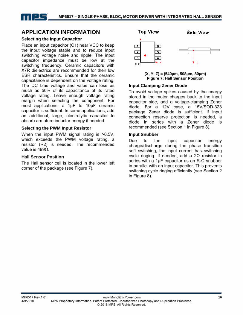
Hall Sensor Position
The Hall sensor cell is located in the lower left corner of the package (see Figure 7).
(X, Y, Z) = (540µm, 508µm, 80µm) Figure 7: Hall Sensor Position
Input Clamping Zener Diode
To avoid voltage spikes caused by the energy stored in the motor charges back to the input capacitor side, add a voltage-clamping Zener diode. For a 12V case, a 15V/SOD-323 package Zener diode is sufficient. If input connection reserve protection is needed, a diode in series with a Zener diode is recommended (see Section 1 in Figure 8).
Input Snubber
Due to the input capacitor energy charge/discharge during the phase transition soft switching, the input current has switching cycle ringing. If needed, add a 2Ω resistor in series with a 1µF capacitor as an R-C snubber in parallel with an input capacitor. This prevents switching cycle ringing efficiently (see Section 2 in Figure 8).

MP6517 – SINGLE-PHASE, BLDC, MOTOR DRIVER WITH INTEGRATED HALL SENSOR
MP6517 Rev.1.01 www.MonolithicPower.com 17 4/9/2018 MPS Proprietary Information. Patent Protected. Unauthorized Photocopy and Duplication Prohibited. © 2018 MPS. All Rights Reserved.
TYPICAL APPLICATION CIRCUIT
OUT2
GND1
2
3
6
5
4
VCC
PWMFG/RD
OUT1
MotorC1
Vin
R2R1
Section1(Optional)
Section2(Optional)
(Optional) (Optional) Figure 8: Typical Application Circuit for 12V VCC Input

MP6517 – SINGLE-PHASE, BLDC, MOTOR DRIVER WITH INTEGRATED HALL SENSOR
MP6517 Rev.1.01 www.MonolithicPower.com 18 4/9/2018 MPS Proprietary Information. Patent Protected. Unauthorized Photocopy and Duplication Prohibited. © 2018 MPS. All Rights Reserved.
PACKAGE INFORMATION
TSOT23-6-SL

MP6517 – SINGLE-PHASE, BLDC, MOTOR DRIVER WITH INTEGRATED HALL SENSOR
NOTICE: The information in this document is subject to change without notice. Users should warrant and guarantee that third party Intellectual Property rights are not infringed upon when integrating MPS products into any application. MPS will not assume any legal responsibility for any said applications.
MP6517 Rev.1.01 www.MonolithicPower.com 19 4/9/2018 MPS Proprietary Information. Patent Protected. Unauthorized Photocopy and Duplication Prohibited. © 2018 MPS. All Rights Reserved.
PACKAGE INFORMATION (continued)
TSOT23-6L