modern vlsi design 2e: chapter 2 copyright 1998 prentice hall ptr topics n basic fabrication steps...
Post on 21-Dec-2015
220 views
TRANSCRIPT

Modern VLSI Design 2e: Chapter 2 Copyright 1998 Prentice Hall PTR
Topics
Basic fabrication steps Transistor structures Basic transistor behavior
Modern VLSI Design 2e: Chapter 2 Copyright 1998 Prentice Hall PTR
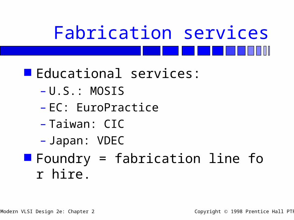
Fabrication services
Educational services:– U.S.: MOSIS– EC: EuroPractice– Taiwan: CIC– Japan: VDEC
Foundry = fabrication line for hire.
Modern VLSI Design 2e: Chapter 2 Copyright 1998 Prentice Hall PTR
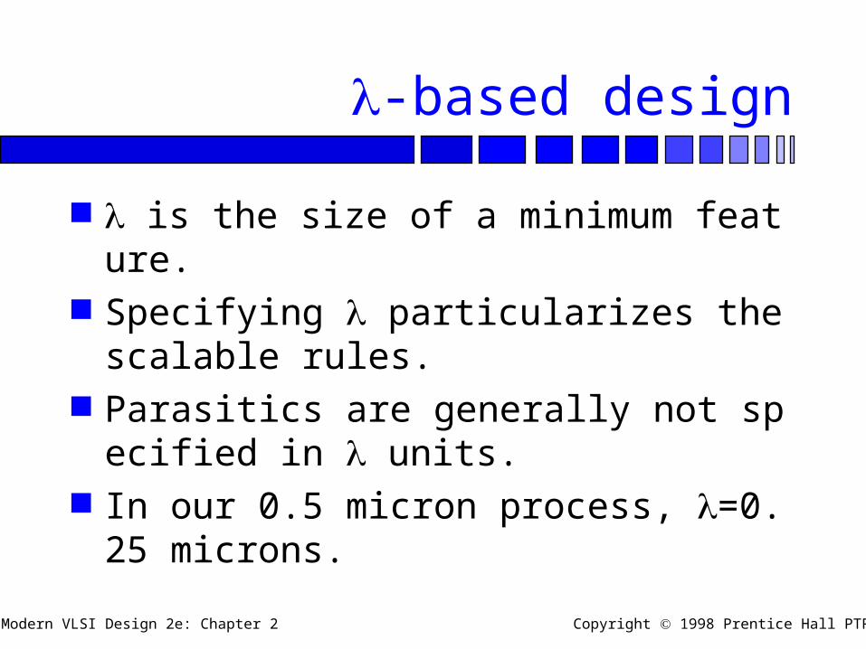
-based design
is the size of a minimum feature. Specifying particularizes the scalable rule
s. Parasitics are generally not specified in un
its. In our 0.5 micron process, =0.25 microns.

Modern VLSI Design 2e: Chapter 2 Copyright 1998 Prentice Hall PTR
Fabrication processes
IC built on silicon substrate:– some structures diffused into substrate;– other structures built on top of substrate.
Substrate regions are doped with n-type and p-type impurities. (n+ = heavily doped)
Wires made of polycrystalline silicon (poly), multiple layers of aluminum (metal).
Silicon dioxide (SiO2) is insulator.

Modern VLSI Design 2e: Chapter 2 Copyright 1998 Prentice Hall PTR
Photolithography
Mask patterns are put on wafer using photo-sensitive material:

Modern VLSI Design 2e: Chapter 2 Copyright 1998 Prentice Hall PTR
Process steps
First place tubs to provide properly-doped substrate for n-type, p-type transistors:
p-tub p-tub
substrate

Modern VLSI Design 2e: Chapter 2 Copyright 1998 Prentice Hall PTR
Process steps, cont
Pattern polysilicon before diffusion regions:
p-tub p-tub
poly polygate oxide

Modern VLSI Design 2e: Chapter 2 Copyright 1998 Prentice Hall PTR
Process steps, cont
Add diffusions, performing self-masking:
p-tub p-tub
poly poly
n+n+ p+ p+

Modern VLSI Design 2e: Chapter 2 Copyright 1998 Prentice Hall PTR
Process steps, cont
Start adding metal layers:
p-tub p-tub
poly poly
n+n+ p+ p+
metal 1 metal 1
vias

Modern VLSI Design 2e: Chapter 2 Copyright 1998 Prentice Hall PTR
Transistor structure
n-type transistor:
Modern VLSI Design 2e: Chapter 2 Copyright 1998 Prentice Hall PTR
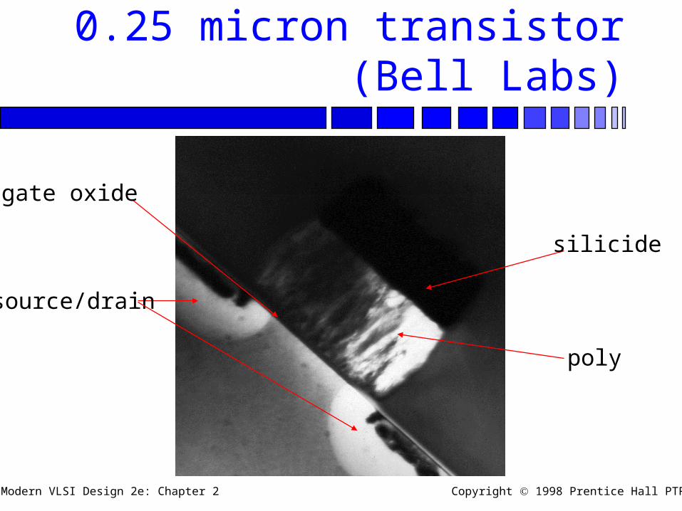
0.25 micron transistor (Bell Labs)
poly
silicide
source/drain
gate oxide

Modern VLSI Design 2e: Chapter 2 Copyright 1998 Prentice Hall PTR
Transistor layout
n-type (tubs may vary):
w
L

Modern VLSI Design 2e: Chapter 2 Copyright 1998 Prentice Hall PTR
Drain current characteristics

Modern VLSI Design 2e: Chapter 2 Copyright 1998 Prentice Hall PTR
0.5 m transconductances
From a 0.5 micron process: n-type:
– kn?= 73 A/V2
– Vtn = 0.7 V
p-type:– kp?= 21 A/V2
– Vtp = -0.8 V

Modern VLSI Design 2e: Chapter 2 Copyright 1998 Prentice Hall PTR
Current through a transistor
Use 0.5 m parameters. Let W/L = 3/2. Measure at boundary between linear and saturation regions.
Vgs = 2V:
Id 0.5k?W/L)(Vgs-Vt)2= 93 A
Vgs = 5V:
Id = 1 mA

Modern VLSI Design 2e: Chapter 2 Copyright 1998 Prentice Hall PTR
Basic transistor parasitics
Gate to substrate, also gate to source/drain. Source/drain capacitance, resistance.
Modern VLSI Design 2e: Chapter 2 Copyright 1998 Prentice Hall PTR
Basic transistor parasitics, cont
Gate capacitance Cg. Determined by active area.
Source/drain overlap capacitances Cgs, Cgd. Determined by source/gate and drain/gate overlaps. Independent of transistor L.– Cgs = Col W
Gate/bulk overlap capacitance.

Modern VLSI Design 2e: Chapter 2 Copyright 1998 Prentice Hall PTR
Latch-up
CMOS ICs have parastic silicon-controlled rectifiers (SCRs).
When powered up, SCRs can turn on, creating low-resistance path from power to ground. Current can destroy chip.
Early CMOS problem. Can be solved with proper circuit/layout structures.

Modern VLSI Design 2e: Chapter 2 Copyright 1998 Prentice Hall PTR
Parasitic SCR
circuit

Modern VLSI Design 2e: Chapter 2 Copyright 1998 Prentice Hall PTR
Parasitic SCR structure
I-V behavior

Modern VLSI Design 2e: Chapter 2 Copyright 1998 Prentice Hall PTR
Solution to latch-up
Use tub ties to connect tub to power rail. Use enough to create low-voltage connection.

Modern VLSI Design 2e: Chapter 2 Copyright 1998 Prentice Hall PTR
Tub tie layout
metal (VDD)
p-tub
p+

Modern VLSI Design 2e: Chapter 2 Copyright 1998 Prentice Hall PTR
Body effect
Reorganize threshold voltage equation:
Vt = Vt0 + Vt
Threshold voltage is a function of source/substrate voltage Vsb.
Body effect is the coefficienct for the Vsb dependence factor.
Modern VLSI Design 2e: Chapter 2 Copyright 1998 Prentice Hall PTR
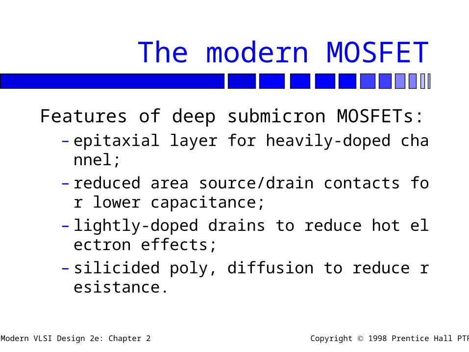
The modern MOSFET
Features of deep submicron MOSFETs:– epitaxial layer for heavily-doped channel;– reduced area source/drain contacts for lower ca
pacitance;– lightly-doped drains to reduce hot electron effe
cts;– silicided poly, diffusion to reduce resistance.

Modern VLSI Design 2e: Chapter 2 Copyright 1998 Prentice Hall PTR
Circuit simulation
Circuit simulators like Spice numerically solve device models and Kirchoff laws to determine time-domain circuit behavior.
Numerical solution allows more sophisticated models, non-functional (table-driven) models, etc.

Modern VLSI Design 2e: Chapter 2 Copyright 1998 Prentice Hall PTR
Spice MOSFET models
Level 1: basic transistor equations of Section 2.2; not very accurate.
Level 2: more accurate model (effective channel length, etc.).
Level 3: empirical model. Level 4 (BSIM): efficient empirical model. New models: level 28 (BSIM2), level 47
(BSIM3).

Modern VLSI Design 2e: Chapter 2 Copyright 1998 Prentice Hall PTR
Some (by no means all) Spice model parameters
L, W: transistor length width. KP: transconductance. GAMMA: body bias factor. AS, AD: source/drain areas. CJSW: zero-bias sidewall capacitance. CGBO: zero-bias gate/bulk overlap capacita
nce.

Modern VLSI Design 2e: Chapter 2 Copyright 1998 Prentice Hall PTR
Topics
Wire and via structures Wire parasitics Transistor parasitics

Modern VLSI Design 2e: Chapter 2 Copyright 1998 Prentice Hall PTR
Wires and vias
p-tub
poly poly
n+n+
metal 1
metal 3
metal 2
vias

Modern VLSI Design 2e: Chapter 2 Copyright 1998 Prentice Hall PTR
Metal migration
Current-carrying capacity of metal wire depends on cross-section. Height is fixed, so width determines current limit.
Metal migration: when current is too high, electron flow pushes around metal grains. Higher resistance increases metal migration, leading to destruction of wire.

Modern VLSI Design 2e: Chapter 2 Copyright 1998 Prentice Hall PTR
Metal migration problems and solutions
Marginal wires will fail after a small operating period : infant mortality.
Normal wires must be sized to accomodate maximum current flow:Imax = 1.5 mA/m of metal width.
Mainly applies to VDD/VSS lines.
Modern VLSI Design 2e: Chapter 2 Copyright 1998 Prentice Hall PTR
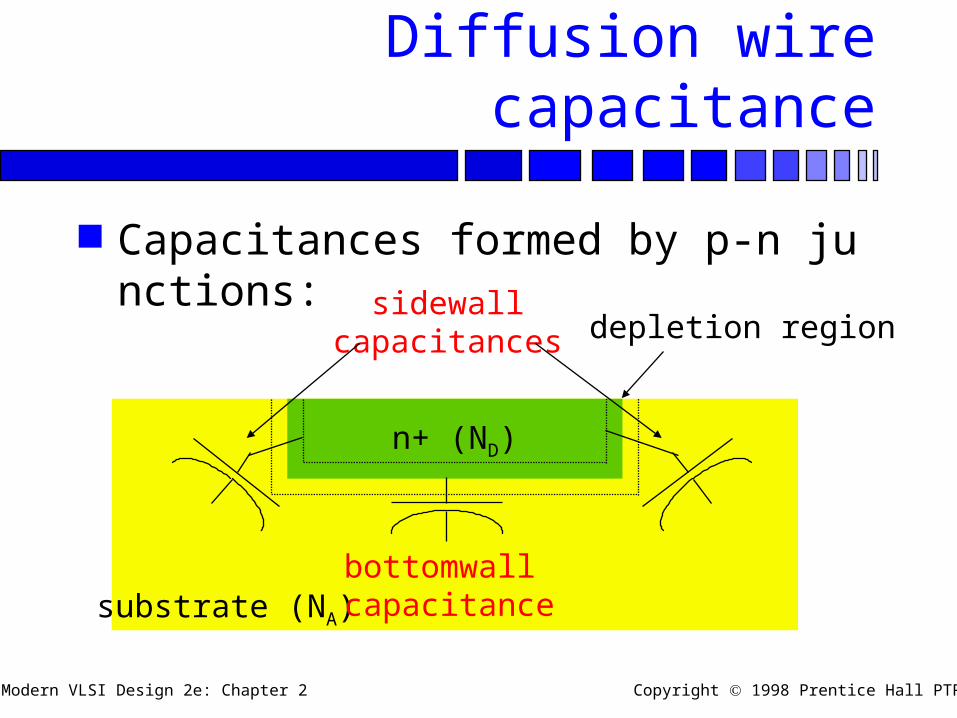
Diffusion wire capacitance
Capacitances formed by p-n junctions:
n+ (ND)
depletion region
substrate (NA)bottomwallcapacitance
sidewallcapacitances

Modern VLSI Design 2e: Chapter 2 Copyright 1998 Prentice Hall PTR
Poly/metal wire capacitance
Two components:– parallel plate;– fringe.
plate
fringe

Modern VLSI Design 2e: Chapter 2 Copyright 1998 Prentice Hall PTR
Metal coupling capacitances
Can couple to adjacent wires on same layer, wires on above/below layers:
metal 2
metal 1 metal 1
Modern VLSI Design 2e: Chapter 2 Copyright 1998 Prentice Hall PTR
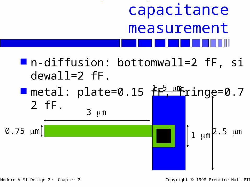
Example: parasitic capacitance measurement
n-diffusion: bottomwall=2 fF, sidewall=2 fF. metal: plate=0.15 fF, fringe=0.72 fF.
3 m
0.75 m 1 m
1.5 m
2.5 m

Modern VLSI Design 2e: Chapter 2 Copyright 1998 Prentice Hall PTR
Wire resistance
Resistance of any size square is constant:

Modern VLSI Design 2e: Chapter 2 Copyright 1998 Prentice Hall PTR
Transistor gate parasitics
Gate-source/drain overlap capacitance:
gate
source drain
overlap

Modern VLSI Design 2e: Chapter 2 Copyright 1998 Prentice Hall PTR
Transistor source/drain parasitics
Source/drain have significant capacitance, resistance.
Measured same way as for wires. Source/drain R, C may be included in Spice
model rather than as separate parasitics.