modelling of the light emitting diode (led) …eprints.utar.edu.my/1811/1/bee-2015-1107144-1.pdf ·...
TRANSCRIPT

MODELLING OF THE LIGHT EMITTING DIODE (LED)
HEATING/ COOLING PROCESS
LOO CHEE MENG
A project report submitted in partial fulfilment of the
requirements for the award of the degree of
Bachelor of Engineering (Hons) Electronic Engineering
Faculty of Engineering and Green Technology
Universiti Tunku Abdul Rahman
January 2015

ii
DECLARATION
I hereby declare that this project report is based on my original work except for
citations and quotations which have been duly acknowledged. I also declare that it
has not been previously and concurrently submitted for any other degree or award at
UTAR or other institutions.
Signature : _________________________
Name : _________________________
ID No. : _________________________
Date : _________________________

iii
APPROVAL FOR SUBMISSION
I certify that this project report entitled “MODELLING OF THE LIGHT
EMITTING DIODE (LED) HEATING/ COOLING PROCESS” was prepared by
LOO CHEE MENG has met the required standard for submission in partial
fulfilment of the requirements for the award of Bachelor of Engineering (Hons)
Electronic Engineering at Universiti Tunku Abdul Rahman.
Approved by,
Signature : _________________________
Supervisor : Dr. Lai Koon Chun
Date : _________________________

iv
The copyright of this report belongs to the author under the terms of the
copyright Act 1987 as qualified by Intellectual Property Policy of Universiti Tunku
Abdul Rahman. Due acknowledgement shall always be made of the use of any
material contained in, or derived from, this report.
© Year, Loo Chee Meng. All right reserved.

v
ACKNOWLEDGEMENTS
I would like to thank everyone who had contributed to the successful completion of
this project. I would like to express my gratitude to my research supervisor, Engr.
Lai Koon Chun for his invaluable advice, guidance and his enormous patience
throughout the development of the research.

vi
MODELING OF THE LIGHT EMITTING DIODE (LED)
HEATING/ COOLING PROCESS
ABSTRACT
This research paper illustrated how LED modeling done using FloTHERM software.
Different materials of heat sink will be tested, compared and discussed in the
research. Next, designed heat sink will be analyzed for its heat dissipation and heat
transferring toward the whole area of the heat sink through parametric studies. High
power LED package will be modeled using CFD software and attached on heat sink
to perform analyses to verify and observe the heat dissipation and heat transfer
between LED towards heat sink. There are two main research objectives contribute
toward this research which are; 1st analyze the heat dissipation of the LED package
and 2nd
improve design for the better cooling performance of the LED. Research will
be contribute for the optimal and reliable operation with no catastrophic failure.

vii
TABLE OF CONTENTS
DECLARATION ii
APPROVAL FOR SUBMISSION iii
ACKNOWLEDGEMENTS v
ABSTRACT vi
TABLE OF CONTENTS vii
LIST OF TABLES ix
LIST OF FIGURES x
LIST OF SYMBOLS / ABBREVIATIONS xv
CHAPTER
1 INTRODUCTION 1
1.1 Background Error! Bookmark not defined.
1.2 Problem Statements 2
1.3 Aims and Objectives 4
1.4 Outline of the report 4
2 LITERATURE REVIEW 6
2.1 Literature review 6
2.2 Theoritical Studies 9
2.2.1 Heat transfer 9
2.2.2 Thermal resistance 10
2.2.3 Simulation 14
2.3 Software implemented CFD 15
2.3.1 STAR CCM+ 15
viii
2.3.2 SolidWorks Error! Bookmark not defined.
2.3.3 Mentor Graphic 18
2.3.4 ANSYS 19
3 METHODOLOGY 21
3.1 Heat sink design 21
3.2 Using FLOTHERM 24
3.2.1 Heat sink design 24
3.2.2 LED design 31
4 RESULTS AND DISCUSSIONS 33
4.1 LED parametric studies 33
4.1.1 PCB materials 33
4.1.2 LED chip and TIM 36
4.1.3 Sizes of LED chip and total power 39
4.1.3.1 Single LED chip package 39
4.1.3.2 2 LED chip package 43
4.1.3.3 4 LED chip package 47
4.2 Heat sink parametric design 51
5 CONCLUSION AND RECOMMENDATIONS 59
5.1 Conclusion 59
5.2 Recommendations 61
REFERENCES 62

ix
LIST OF TABLES
TABLE TITLE PAGE
3.1 Material list for LED package 32
4.1 Result of two PCB materials compared 34
4.2 Comparison of maximum operating junction
temperature for GaN, GaP and AIN materials for
LED chip 37
4.3 Result of maximum operating junction temperature
of single LED chip package for two types of LED
chip materials 39
4.4 Result of maximum operating junction temperature
of 2 LED chip package for two types of LED chip
materials 45
4.5 Result of maximum operating junction temperature
of 4 LED chip package for two types of LED chip
materials 47
4.6 Parametric studies for Heat sink's base thickness
0.15cm 51
4.7 Parametric studies for Heat sink's base thickness
0.2cm 51
4.8 Parametric studies for Heat sink's base thickness
0.25cm 52
5.1 LED package's material recommendation 61
5.2 LED package's size recommendation 61
5.3 Heat sink's design recommendation 61

x
LIST OF FIGURES
FIGURE TITLE PAGE
2.1 Equivalent thermal circuit of LED package 11
2.2 Structure model of the LED package 12
2.3 Flux density distribution, PC-FEA running the i-Ψ-
GoFER for a certain rotor position 15
2.4 Temperature distribution for both load case 1000
rpm and 6000 rpm 16
2.5 Simulations using SolidWorks CFD software 17
2.6 The Mentor Graphics MicReD T3Ster Thermal
Measurement System characterizes critical LED
thermal parameters 18
2.7 Temperature distribution of finite element
simulation 19
3.1 Front view of heat sink 21
3.2 Side view of Heat sink 22
3.3 Top view of Heat sink 22
3.4 Actual measurement for front view 23
3.5 Actual measurement for side view 23
3.6 Actual measurement for top view 24
3.7 Create a new project from FLOTHERM user
interface 24
3.8 Select "Assembly" from the panel and then select
"Heat sink" 25

xi
3.9 Select the dimension for the Heat sink 25
3.10 Select the requirement for fins of the Heat sink 26
3.11 Select the material for the Heat sink 26
3.12 Decompress the Heat sink for further details
setting 27
3.13 After decompression for the Heat sink 27
3.14 Adding a cuboid to the Heat sink 28
3.15 Compact Heat sink design is completed 28
3.16 Compact Heat sink layout 29
3.17 Create cut off for the Heat sink 29
3.18 The outline of the cut off for the Heat sink 30
3.19 After cut off for the Heat sink 30
3.20 Create LED package 31
3.21 Create layers for LED package 31
3.22 Completed layers for LED package 32
3.23 Compact LED package design layout 32
4.1 Result of 1 mm2 GaN single chip LED package
with FR-4 PCB material and ALO for TIM of 0.5
W 33
4.2 Result of 1 mm2 GaN single chip LED package
with MCPCB PCB material and ALO for TIM of
0.5 W 34
4.3 Operating junction temperature FR-4 vs MCPCB
for different types of TIM of 0.5 W 35
4.4 Result of 1 mm2 GaP single chip LED package
with MCPCB PCB material and ALO for TIM of
0.5 W 36
4.5 Result of 1 mm2 AIN single chip LED package
with MCPCB PCB material and ALO for TIM of
0.5 W 37

xii
4.6 Maximum operating junction temperature for GaN,
GaP and AIN materials 38
4.7 Maximum operating junction temperature for
single LED chip for different dimension (1, 1.5 and
2) mm2 of heat sink ranging total power from
0.5W to 1W 39
4.8 Graph of total power vs temperature for different
sizes of single GaN LED chip 40
4.9 Graph of total power vs temperature for different
sizes of single AIN LED chip 40
4.10 Result of 1.5 mm2 GaN single chip LED package
with MCPCB PCB material and ALO for TIM for
0.5W 41
4.11 Result of 1.5 mm2 GaN single chip LED package
with MCPCB PCB material and ALO for TIM for
1W 41
4.12 Result of 1.5 mm2 AIN single chip LED package
with MCPCB PCB material and ALO for TIM for
0.5W 42
4.13 Result of 1.5 mm2 AIN single chip LED package
with MCPCB PCB material and ALO for TIM for
1W 42
4.14 Result of 1 mm2 AIN 2 chip LED package with
MCPCB PCB material and ALO for TIM for 2 W 43
4.15 Result of 1.5 mm2 AIN 2 chip LED package with
MCPCB PCB material and ALO for TIM for 2 W 44
4.16 Result of 2 mm2 AIN 2 chip LED package with
MCPCB PCB material and ALO for TIM for 2 W 44
4.17 Maximum operating junction temperature for 2
LED chip for different dimension (1, 1.5 and 2)
mm2 of heat sink ranging total power from 1W to
2W 45
4.18 Graph of total power vs temperature for different
sizes of 2 GaN LED Chip 46
4.19 Graph of total power vs temperature for different
sizes of 2 AIN LED Chip 46

xiii
4.20 Graph of total power vs temperature for different
sizes of 4 GaN LED Chip 47
4.21 Graph of total power vs temperature for different
sizes of 4 AIN LED Chip 48
4.22 Maximum operating junction temperature for
4LED chip for different dimension (1, 1.5 and 2)
mm2 of heat sink ranging total power from 2W to
4W 48
4.23 Result of 1 mm2 AIN 4 chip LED package with
MCPCB PCB material and ALO for TIM for 4 W
78.5°C 49
4.24 Result of 1.5 mm2 AIN 4 chip LED package with
MCPCB PCB material and ALO for TIM for 4 W
77.4°C 49
4.25 Result of 2 mm2 AIN 4 chip LED package with
MCPCB PCB material and ALO for TIM for 4 W
77.4°C 50
4.26 Maximum operating junction temperature for
single 2mm2 LED chip for different heat sink size
(3, 4 and 5) cm2, heat sink's fin thickness and
height and heat sink's base thickness 1.5mm of
total power 0.5 Watt 52
4.27 Maximum operating junction temperature for
single 2mm2 LED chip for different heat sink size
(3, 4 and 5) cm2, heat sink's fin thickness and
height and heat sink's base thickness 2mm of total
power 0.5 Watt 53
4.28 Maximum operating junction temperature for
single 2mm2 LED chip for different heat sink size
(3, 4 and 5) cm2, heat sink's fin thickness and
height and heat sink's base thickness 2.5mm of
total power 0.5 Watt 53
4.29 Result of 2 mm2 AIN single chip LED package on
3cm2, 2.56cm height and 1mm thickness heat sink
for 0.5 W 46.8°C 54
4.30 Result of 2 mm2 AIN single chip LED package on
3cm2, 2.76cm height and 1mm thickness heat sink
for 0.5 W 46.1°C 55

xiv
4.31 Result of 2 mm2 AIN single chip LED package on
3cm2, 2.96cm height and 1mm thickness heat sink
for 0.5 W 46.6°C 55
4.32 Result of 2 mm2 AIN single chip LED package on
4cm2, 2.56cm height and 1mm thickness heat sink
for 0.5 W 34.2°C 56
4.33 Result of 2 mm2 AIN single chip LED package on
4cm2, 2.76cm height and 1mm thickness heat sink
for 0.5 W 33.9°C 56
4.34 Result of 2 mm2 AIN single chip LED package on
4cm2, 2.96cm height and 1mm thickness heat sink
for 0.5 W 33.5°C 57
4.35 Result of 2 mm2 AIN single chip LED package on
5cm2, 2.56cm height and 1mm thickness heat sink
for 0.5 W 34.6°C 57
4.36 Result of 2 mm2 AIN single chip LED package on
5cm2, 2.76cm height and 1mm thickness heat sink
for 0.5 W 34.1°C 58
4.37 Result of 2 mm2 AIN single chip LED package on
5cm2, 2.96cm height and 1mm thickness heat sink
for 0.5 W 33.2°C 58

xv
LIST OF SYMBOLS / ABBREVIATIONS
Pth heat power
Rth thermal resistance
thermal resistance R and thermal capacitance C
k thermal conductivity, W/(mK)
h height, m
g gravity, m/s2
µ viscosity, m2/s
density, kg/m3
compressible flow parameter
v specific volume, m3
t time, s
s strain rate
T temperature, K
P pressure, kPa
PCB printed circuit board
TIM thermal interface material
GaN gallium nitride
InGaN indium gallium nitride
AIN aluminium nitride
GaP gallium phosphide
LED light emitted diode
MCPCB metal core printed circuit board
ALO aluminium oxide

1
CHAPTER 1
1 INTRODUCTION
1.1 Background
Due to the influence of green technology, light bulb which commonly used in
centuries has replaced by light emitting diode (LED) nowadays due to its power
efficiency, power saving concern and longer lifespan. Since then, it was often
manufactured as multi package module instead of single package due to the
luminosity demand and cost concern. LED technologies has been seen applying in
most applications where power efficiency is essential from household lighting,
television display, car headlights to digital signage and more.
Nevertheless, the uniformity of temperature gradient may generate
unbalanced stress along the multi package interface, resulting lifespan and output
degradation. It is hence crucial to predict and model the thermal transfer performance
of the LED module prior to the manufacturing process as to ensure output quality
and prevent catastrophic failure. Despite the apprehensive grown and popularity
of LED, today's LED applications present a complex design challenge. The challenge
required such as current and voltage parameters, safety and power efficiency
regulations, thermal management for better reliability and longer lifespan, limited
circuit board space and the need to meet time-to-market deadlines must all be
addressed simultaneously (Barb Schmitz, 2014).

2
Computational Fluid Dynamics is a methodology that allows engineers to
predict the performance of their designs to simulate problems involving gases,
liquids and solids and multi-phase problems. CFD is used in the design of almost
every major product. Reducing uncertainty in the design process, increasing of the
productivity and resulting in higher quality products and designs, with greater
robustness to achieved customer's requirements. As such, CFD software are brought
by experts to analyze the thermal spreading effect of the LED.
With the major advances of computational methods, CFD software has been
used for modelling to reduce design time and cost. Due to the advances of the CFD
software, CFD has now emerged as an effective tool towards simulation to measure
and analyze temperature flows and heat transfer for better thermal management. By
using CFD, suitable model of the LED can be generate and identify under various
heating, cooling conditions and different environments before a various type of
experimental done. Thus, it's able to reduce time consuming and period of designing
a low power consumption LED.
Nevertheless in terms of heat dissipation, heat sinks are the most common
hardware component in control of thermal management in electronics. The
responsiveness and effectiveness of thermal control of electronic components which
assemblies and modules by enhancing their surface area through the use of fins.
Applications utilizing fins of the heat sinks for cooling purposes have increased
significantly during the last few decades due to an increase in heat flux densities and
product miniaturization. Today's advanced electronic circuits disperse substantially
heavier loads of heat than ever before. At the same time, the premium associated
with miniaturized applications has never been greater, and space allocated for
cooling purposes is on the decline (R. Sam Sukumar, 2013). These factors have
forced design engineers to seek more efficient heat sink technologies.

3
1.2 Problem Statements
Owing to the excellent color saturation and low power consumption, light emitting
diode (LED) has become widely used in modern lighting applications such as flat-
panel display, street lamps, advertising signage and decorative lighting. LED has
drawn public attentions for its better reliability and lifespan, if compared to the
traditional tungsten and florescence lighting. In order to enhance the luminosity
performance of LED, the electrical driving current is crucial in producing more
lumens. However, in real case most of the input power is lost as heat before
transforming into useful light. The dissipated heat increases the temperature of the
LED and affects its reliability and durability. The rise of temperature gradient can
generate undesired stresses, eventually leads to light output degradation and
catastrophic failure of the LED (Gavin Sullivan & Campbell Edmondson, 2008).
Recently, thermal distribution on multi package LED modules has become a
new study. Modular LED is widely used as flat-panel and signage board as it
generates more lumens at a lower cost. Nevertheless, the uniformity of temperature
gradient may change and generate unbalanced thermal distribution along the module
interface. In order to maintain the output light quality and performance reliability,
thermal distribution analysis such as CFD was carried out to predict the thermal
performance of LED module.
Since LEDs are negatively influenced by high temperature, the thermal
management analysis for them is crucial for improved light quality, reliability and
product lifespan. In this study, a thermal design of finned heat-sink with heat pipes as
passive cooling was applied. the heat pipes can supply high thermal conductivity
with much less weight and volume compared to copper or aluminium base and
consequently less obstruction to air flow with enhanced natural convection. As the
natural convection and radiation dominate heat transfer in this case, the optimum fin
spacing was calculated by the most used empirical correlations.
Then, the design will be numerical investigated by computational Fluid
Dynamics (CFD) to obtain best thermal performance. Meanwhile, the design will be

4
evaluated experimentally as to consistently approve the thermal design compared to
correlations and simulation. As the fin spacing is both optimized by correlations and
modelling, the optimum thermal design can be eventually achieved.
1.3 Aims and Objectives
The objectives of the thesis are shown as following:
i) to study the thermal spreading effect
ii) to model the heat dissipation phenomenon
iii) to deduce the improved design for better thermal management of the LED
1.4 Outline of the Report
Basically in this final year project, since efficiency of light emitting diode (LED) is
highly dependent on the operating current and junction temperature. Whereas in
extreme conditions, high temperature also implies early degradation of the LED
device. Therefore, thermal analyses for LED modules are to be carried out with the
aid of Computational Fluid Dynamic (CFD) software (FloTHERM).
As for a starter, an example of heat sink was given by supervisor. Then
measurements and analyze on heat sink will be carried out. Next, modelling will be
done using FloTHERM software. Different materials of heat sink will be tested,
compared and discussed further onwards. Next, the previously designed heat sink
will be analyzed for its heat dissipation and heat transferring toward the whole area
of the heat sink by using different environment for example: material of the heat sink,
environment temperature, air density and more. The results obtained will be used as
to prove the process of designing heat sink without any error occur. This is important
because when the process brought to next procedure, any small mistake or careless in

5
the process of designing heat sink will caused a problematic results, therefore process
of designing of a heat sink is crucial and more details required.
Next, high power LED module will be modelled using CFD software. Then,
it will be attached on heat sink to perform analyses to verify and observe the heat
dissipation and heat transfer between LED towards heat sink. Besides that,
experimental will be done to verify simulation versus real case are within the range
with minor tolerance. There are two main research objectives contribute toward the
project which are analyze the heat dissipation of the lighting element and improve
design for the better cooling performance of the LED. Research will be contribute for
the optimal and reliable operation with no catastrophic failure.

6
CHAPTER 2
2 LITERATURE REVIEW
2.1 Literature review
Siang Ling Oon 2010, using Computational Fluid Dynamic modeling technique to
simulate LED package-on-substrate with a heat sink on top. The results shown
details information of heat sink models with best possible results compared to actual
measurements; however, a full details of heat sink model are very time consuming.
The compact design version of heat sink model is only desired for fast analysis
purposes. The result obtained for percentage error is justifiable for industrial
applications and yet save more time.
Sridhar Narasimhan et al. 2003, reduced the computational method by
creating heat sink using a compact “porous block” model, with a fine thermal
conductivity and pressure loss co-efficient. From the study, parallel plate heat sinks
which situated in laminar will imposed a convection. This methodology will
determine thermal properties of compact heat sink models and thus provide a high
level of accuracy. The results proved the data generated from using porous block
compact model is legit. Other than that, porous-block representation can achieve
outstanding acceptance to predict the thermal characteristics of a heat sinks.
Kevin R. Anderson et al. 2013, using CFD simulations to simulate heat and
fluid flow performance in a electronic package through a large power dissipations of
1000 W/m2. A combination of thermal control using high thermal conductivity
materials will forced convection cooling by using DC fans. While the internal forced
convection heat transfer using a pumped fluid loop cold plate/heat exchanger system)

7
to simulate the advantage of using COTS components to accomplish a thermal
control solution. The results obtained are equivalent with previous studies which
involving electronics cooling simulations.
Linton, R.L. et al. 1995, compared the results of a detailed CFD model of a
heat sink with a set of experimental data. He use a his technique to represent the heat
sink with a specific CFD model and compared with the detailed CFD model. Result
indicated that his technique can be used when designing heat sinks for larger card or
system models.
Mohammed H. S. Al Ashry 2015, made an attempt to prove the theoretical
model by design a heat sink with a lower temperature gradient than PCB excess heat.
The key of heat sink design is to sample the parts situated in central areas within the
circuit board for better direct access to the heat source for better engagement.
Experiments proved that increased convective air flow velocity will decreased
conductive resistance on the surface of the heat sink. This feature is very persuasive
and puts attention on the deploying forced convective air flow.
Dong Mei Li et al. 2009, designed a water miniature heat pipe to dissipate
heat based on the LED packaging structure. Result is junction temperature of the
source achieved below 70°C at condition of natural convection. The result matched
with the requirement of the LED working below 120°C and result shows that heat
pipe is the effective solution for the LED light application dissipation. Consideration
for lower junction temperature are divided to three major requirement which are
height, thickness and fin numbers. According to simulation results, the ideal scheme
achieved when the lower junction temperature is 56.7°C obtained by using few
combination of optimization levels.
Bor Jang Tsai et al. 2011, simulated the temperature distribution under
natural convection using numerical analysis and by introducing spherical coordinate
system change in heat resistance. In addition to illuminating the heat dissipation of
multi-chip LED modules, they attempts to identify the problems that affecting the
temperature distributions of LEDs. Simulation results obtained and the temperature
of a multi-chip LED module is slightly less than that of linear superposition. Thus,

8
simulation result confirms the effectiveness, workable and accuracy of the proposed
thermal resistance formula in the work.
Yan Lai et al. 2006, investigated an active liquid cooling solution to improve
LED's application on automotive headlights. The investigation of thermal design
completed from device to board to system level has been carried out throughout the
research. Both methods of air cooling and passive liquid cooling are investigated and
eliminated due to the methods unable to maintain temperature of LED junction under
its maximum tolerated levels which unable to accept in the actual application.
Therefore, only an active liquid cooling solution is nominated in terms of its suitable
thermal management solution.
András Poppe et al. 2008, discussed about thermal characterization of
packaged semiconductor devices by perform thermal simulations and measurements.
Simulation is the priority to be done before production to be done. There are some
difficulties to create an ideal simulation models since the actual time-constants of
heat sink are small. They believe that combined thermal and radiometric
measurements for power LEDs will become a standard some day.
Gábor Farkas et al. 2004, proved that the structure function approach is a
powerful method for characterizing the heat conductance path and calculating
junction-to-case thermal resistances. They also proposed to design a compact LED
model with different complexity levels, where by experimental result able to describe
some measured thermal effects and proceed to the electro-thermal simulation. The
design model will reflects the changes of Rth at different currents and generate
different temperature transients using the model of LED arrays with active
components which allowed all transient junction temperatures and board temperature
calculated and plotted.
Kai Lin Pan et al. 2014, studied the reliable thermal resistance calculation
method by using theoretical mathematics calculation, experimental testing and finite
element simulation based on the thermal resistance network model and the principle
of steady state heat transfer. After that, she achieved experimental result with 9.2 %,

9
and the error of total thermal resistance between the experimental result and finite
element simulation with difference of -3.9 %.
2.2 Theoretical studies
2.2.1 Heat transfer
As previously mentioned in literatures, heat transfer characteristics of the LED
package can be analyzed by the structure function method. It discusses the heat
capacity parameters and thermal conductivity of the properties along the one-
directional heat flow path. In order to derive the structure function, the thermal
evaluations were firstly identified, followed by the heating or cooling curves. By
transforming the curves, the structure function can be thus determined. The function
relates to a time-constant system, in which the time constant, is a function of
thermal resistance R and thermal capacitance C. According to (Székely 1991),
detailed response of the structure function is calculated as:
n
iithithj tRPtT
1
/exp1)(
(1)
where Pth is the heat power and Rth is the resistance. The function approaches infinity
in a real distributed system, and Eq. (1) can be rewritten as:
dtRPtT thj
0
/exp1)(
(2)
In relate to the time constant spectrum, Eq. (2) can be viewed as:
dzzRPzTdz
dthj
expexp
(3)

10
where z = ln(t) and = ln(). The derivative of z is then expressed:
zWzRPzT
dz
dthj
(4)
where W(z) = exp[z - exp(z)]. The symbol denotes the convolution operation.
Besides, the structure function can be represented by a distributed RC thermal system,
in which the sum of thermal capacitances and sum of thermal resistances are derived
as Eqs. (5) and (6), respectively:
x
dAcC
0
(5)
x
A
dR
0
(6)
The differential structure function can be therefore determined:
)()()( 2 xAxxcdR
dCRQ
(7)
where c(x) is the volumetric heat capacitance, (x) is thermal conductivity and A(x) is
cross sectional area of the heat flow.
2.2.2 Thermal resistance
In order to determine the thermal resistance (Rth), the schematic of LED package
shown in Figure 1 can be transformed into the thermal circuit, as shown in Figure 2.

11
Fig. 2.1: Equivalent thermal circuit of LED package.
For the single chip LED package, the thermal resistance for the entire system can be
estimated as:
kheatTIMsubstratepastesolderslugattachdiedietot RRRRRRRR sin
(8)
If the low conductivity materials were used, i.e. silicon die attach, Ag solder paste
and grease as TIM, Eq. (8) can be simplified as:
kheatsubstrateslugdietot RRRRR sin (9)
By assuming a uniform heat flux on the top of chip, the thermal resistance of chip
can be described with one-dimensional thermal resistance model for heat diffusion:
diedie
diedie
Ak
tR
(10)
where t is the thickness, k is the thermal conductivity and A is the cross sectional area.
Similarly, thermal resistance of the slug can be expressed as:

12
slugslug
slugslug
Ak
tR
(11)
The structure model of the LED package with multiple chips is shown in Figure 3.
The LED chip is with an area of cd with center coordinate of (Xi, Yi), mounted on
the heat spreader measured in ab. In general, the heat spreader was insulated on all
surfaces, except the bottom which left exposed to ambient.
Fig. 2.2: Structure model of the LED package.
A general analytical solution based on separation variable method can be employed
for temperature estimation on rectangular flux channels. The solution for the
temperature distribution on the heat sink, which calculates the temperature of
multiple chips LED package, was stated as (Cheng et al., 2010):
N
iif zyxTTzyxT
1
,,),,(
(12)
where Tf is the ambient temperature, T(x,y,z) is temperature of LED at the coordinate
(x,y,z), N is the number of chip and i measures the total temperature excess of the
module. The following equation is to express the surface temperature distribution of
LED module at z = 0:

13
xxAxAxAAyxim n
imn
n
in
m
im
i coscoscoscos0,,1 111
0
(13)
Several Fourier coefficients, i.e. Am, An and Amn must be determined in order to
obtain the temperature excess. A0 is the value for the coefficient in uniform flow and
calculated by:
10
k
t
ab
QA
(14)
where indicated the heat transfer coefficient of the LED to base, k is the thermal
conductivity of heat spreader and Q is the dissipation power. The Fourier coefficients
can be determined by:
mmi
iimiimim
kabc
cXcXQA
2
2/2sin2/2sin2
(15)
nni
iiniinin
kabd
dYdYQA
2
2/2sin2/2sin2
(16)
nmnmnmii
inininimimn
kdabc
dycXQA
,,
2/sincos2/sincos16
(17)
where = m/a, = n/b and = (2 + 2
)0.5
. For the multiple chip LED package,
says N N array, the total thermal resistance can be determined by using the
following equation:
kheatsubstrateslugdietot RNRRRR sin (18)
The last term in Eq. (18) can be obtained by considering the innermost LED which
gives a maximum junction temperature:
14
NQ
yxTRN kheat
0,,sin
(19)
2.2.3 Simulation
Simulation study of the LED package can be made with the professional thermal
analysis software. The software Flotherm can be utilized to perform the thermal
modeling work. With the embedded CFD solver, Flotherm is able to solve the
Navier-Stokes equations for mass, momentum and energy conservation with the
finite volume technique (Panton, 1996). The equation for mass can be expressed as:
vvt
(20)
where is the density, t is the time and v is the velocity vector. Momentum is
another vector measurement which is in the same direction as velocity and calculated
as:
Svgpvvt
v
267.0
(21)
where p is the pressure, g is the gravity, is the viscosity and S is the strain rate
tensor. The thermal energy is presented as follows:
pv
t
pTSSvTkTv
t
TcP :267.0
2
(22)
where T is the absolute temperature, k is the thermal conductivity and is the
expansiveness. A number of simulation software could be used to perform the
thermal analysis, e.g. Star CCM+ and ANSYS. STAR-CCM+ performs thermal

15
modelling of electric machines and calculates the temperature transient of the system.
STAR-CCM+ is able to solve engineering problems involving fluid flow, conjugate
heat transfer and solid stress. On the other hand, ANSYS allows the design and
optimization of new equipment and to troubleshoot existing installations.
Furthermore, it contains modelling capabilities to model flow, turbulence, heat
transfer, and reactions for real case industrial applications.
2.3 Software Implemented CFD
2.3.1 STAR CCM+
STAR-CCM+ showed new methods of thermal modelling of electric machines using
the combination of an electromagnetic analysis tool to determine the performance
and the temperature transient of the system. STAR-CCM+ able to run engineering
process by solving problems involving fluid flow, conjugate heat transfer and solid
stress. Figure 3 shows the different flux density distributions for the two load cases
with the highly saturated parts in red
a) load point 1000.0 rpm b) load point 6000.0 rpm
Fig. 2.3: Flux density distribution, PC-FEA running the i-Ψ-GoFER for a certain
rotor position

16
Fig. 2.4: Temperature distribution for both load case 1000 rpm and 6000 rpm
For 1000 rpm load case, the winding is hotter than on the left hand side as the
water is already pre heated from the right half. For the 6000.0 rpm load case the
cooling with the minimum temperature drops below the 50°C of the coolant inflow
temperature.
2.3.2 SolidWorks
With SolidWorks Flow Simulation, the designer able to define the system to be used
and select the desired result resolution by meshing all level. The design engineer
defines the project objectives of the analysis and required information to achieve the
ideal result thus monitor those values during the calculation and create a table of the
computed values when the analysis has been completed.
Heat sink without shield Heat sink with shield

17
Fig. 2.5: Simulations using SolidWorks CFD software

18
2.3.3 Mentor Graphic
With Mentor Graphics FloEFD is a proven thermal simulation software environment
that speeds and simplifies the task of LED luminaire and system design. Engineers
test new ideas with “what-if” simulations rather than expensive hardware prototypes.
And important issues like internal and external temperatures and heat flows can be
evaluated quickly and accurately.
Fig. 2.6: The Mentor Graphics MicReD T3Ster Thermal Measurement System
characterizes critical LED thermal parameters.

19
2.3.4 ANSYS
ANSYS allows design engineer to predict an engineering process with confidence by
input details of information to a user friendly interface before manufacturing process
began. This software has the analysis capabilities to design and optimize new
equipment and to troubleshoot existing installations. Furthermore, it contains
modeling capabilities to model flow, turbulence, heat transfer, and reactions for real
case industrial applications. Figures below showed that CFD software simulate
simulation of heat dissipation from LED package throughout heat sink

20
Fig. 2.7: Temperature distribution of finite element simulation.

21
CHAPTER 3
3 METHODOLOGY
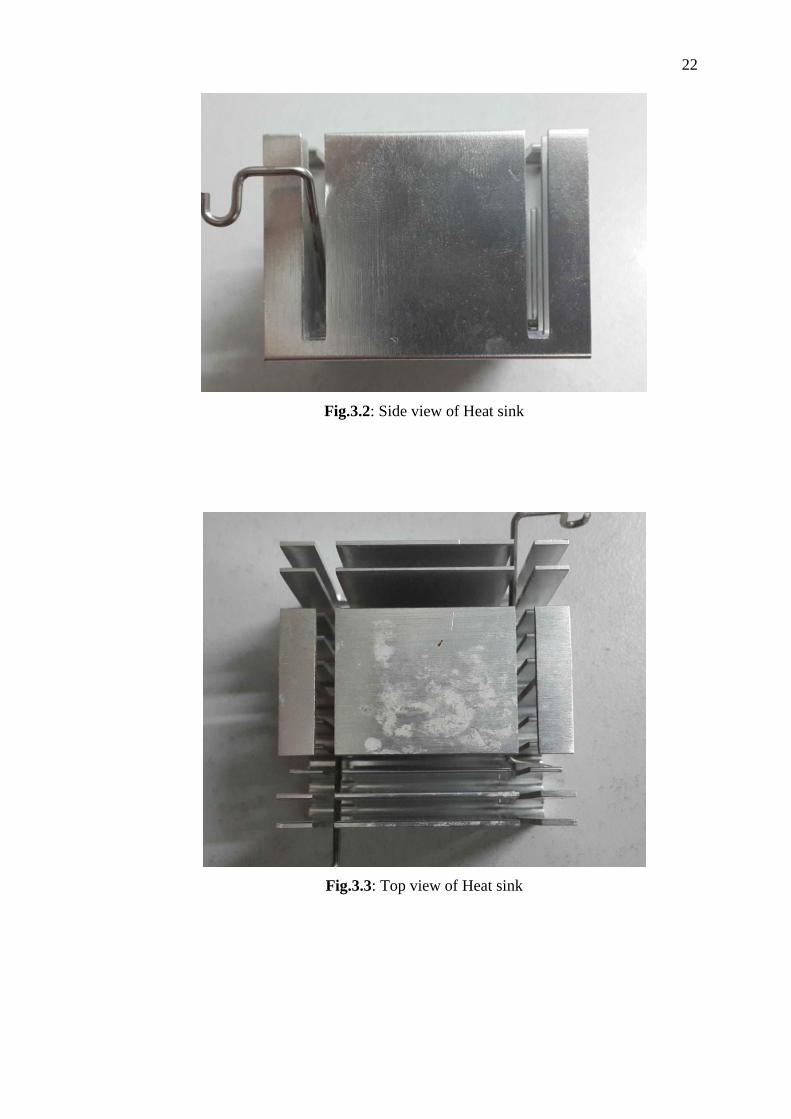
3.1 Heat sink Design
Fig.3.1: Front view of Heat sink
22
Fig.3.2: Side view of Heat sink
Fig.3.3: Top view of Heat sink

23
Fig.3.4: Actual measurement for front view
Fig.3.5: Actual measurement for side view

24
Fig.3.6: Actual Measurement for top view
3.2 Using FLOTHERM
3.2.1 Heat sink design
Fig.3.7: Create a new project from FLOTHERM user interface

25
Fig.3.8: Select "Assembly" from the panel and then select "Heat sink"
Fig.3.9: Select the dimension for the Heat sink

26
Fig.3.10: Select the requirement for fins of the Heat sink
Fig.3.11: Select the material for the Heat sink

27
Fig.3.12: Decompress the Heat sink for further details setting
Fig.3.13: After decompression for the Heat sink

28
Fig.3.14: Adding a cuboid to the Heatsink
Fig.3.15: Compact Heat sink design is completed

29
Fig.3.16: Compact Heat sink layout
Fig.3.17: Create cut off for the Heat sink

30
Fig.3.18: The outline of the cut off for the Heat sink
Fig.3.19: After cut off for the Heat sink

31
3.2.2 LED DESIGN
Fig.3.20: Create LED package
Fig.3.21: Create layers for LED package

32
Fig.3.22: completed layers for LED package
Fig.3.23: Compact LED package design layout
Table.3.1: Material list for LED package
Type Materials (W/m.K)
LED GaN/InGaN 130
LED AIN 285
LED GaP 110
Substrate Heat Slug 386
PCB FR-4 0.3
PCB MCPCB 201
TIM Grease 4.1
TIM ALO 25
TIM Film 3
TIM Tape 0.6
LED chip
Heat slug
PCB
TIM

33
CHAPTER 4
4 RESULTS AND DISCUSSIONS
4.1 LED PARAMETRIC STUDIES
4.1.1 PCB materials
Fig.4.1: Result of 1 mm2 GaN single chip LED package with FR-4 PCB material and
ALO for TIM of 0.5 W

34
Fig.4.2: Result of 1 mm2 GaN single chip LED package with MCPCB PCB material
and ALO for TIM of 0.5 W
Table.4.1: Result of two PCB materials compared
Chip Size CHIP PCB TIM Power Temperature
No. W X L Material Material Material Watt Min Max
1 1 x 1 GaN FR-4 Grease 0.5 31.3 135
mm2 ALO 0.5 31.3 130
FILM 0.5 31.3 141
TAPE 0.5 31.3 166
MCPCB Grease 0.5 31.4 36.6
ALO 0.5 31.4 34.8
FILM 0.5 31.4 38.6
TAPE 0.5 31.4 47.6

35
Fig.4.3: Operating junction temperature FR-4 vs MCPCB for different types of TIM
of 0.5 W
Figure 31 shown the result of implementing 1 x 1 mm2 GaN/InGaN single LED
package with FR-4 as PCB material and as well as ALO for TIM (Thermal interface
material). From table 2 and graph 2, the result obtained when using FR-4 as PCB
material which maximum operating junction temperature achieved is 130°C. Since
the optimum operating junction temperature for LED package must not exceed 90-
120°C, therefore FR-4 material omitted. MCPCB (metal core PCB) material adopted
for the PCB and simulation verified that MCPCB done a better job for heat
dissipation compared to FR-4 where the result obtained is 34.8°C by implementing
ALO material for TIM layer compared to 130°C from FR-4.
Based from the comparison of the result for different types of TIM layer,
ALO for TIM layer perform the better task for heat dissipation which yield 34.8°C
while grease material yield 36.6°C, film material yield 38.6°C and tape material yield

36
47.6°C. To put it in a nutshell, ALO is suitable for better thermal conductivity
compared to other materials..
4.1.2 LED chip and TIM materials
Fig.4.4: Result of 1 mm2 GaP single chip LED package with MCPCB PCB material
and ALO for TIM of 0.5 W

37
Fig.4.5: Result of 1 mm2 AIN single chip LED package with MCPCB PCB material
and ALO for TIM of 0.5 W
Table.4.2: Comparison of maximum operating junction temperature
for GaN, GaP and AIN materials for LED Chip
Temperature °C
TIM Materials LED Chip materials
GaN GaP AIN
Grease 36.6 36.7 36.3
ALO 34.8 34.9 34.5
FILM 38.6 38.7 38.4
TAPE 47.6 47.7 47.4

38
Fig.4.6: Maximum operating junction temperature for GaN, GaP and AIN materials
From table 2, the result shown that AIN material perform the best operating junction
temperature which yield 36.3°C for Grease material, 34.5°C for ALO material,
38.4°C for Film material and 47.4°C. Throughout the comparison, the actual result
for three types material induced a similar result therefore GaN and AIN material
were chosen to proceed for next task since GaN material is widely used by
semiconductor industrial to develop LED chip due to its stability and convenient of
implementation while AIN material is new to market which is expensive and due to
its complicated process thus perform an excellent thermal conductivity. GaN/InGaN
and AIN materials, heat slug, MCPCB and ALO is finalized as good thermal
conductivity LED package.

39
4.1.3 Sizes of LED Chip and total power
4.1.3.1 Single LED chip package
Table.4.3: Result of maximum operating junction temperature of single LED chip
package for two types of LED chip materials
Sizes (mm2)
Chip 1 1.5 2
Materials 0.5 W 1 W 0.5 W 1 W 0.5 W 1 W
GaN 34.8 44.6 34 42.9 33.7 42.5
AIN 34.8 44.1 33.9 42.7 33.7 42.4
Fig.4.7: Maximum operating junction temperature for single LED chip for different
dimension (1, 1.5 and 2) mm
2 of heat sink ranging total power from 0.5W to 1W

40
Fig.4.8: Graph of total power vs temperature for different
sizes of single GaN LED Chip
Fig.4.9: Graph of total power vs temperature for different
sizes of single AIN LED Chip

41
Fig.4.10: Result of 1.5 mm2 GaN single chip LED package with
MCPCB PCB material and ALO for TIM for 0.5 W
Fig.4.11: Result of 1.5 mm2 GaN single chip LED package with MCPCB PCB
material and ALO for TIM for 1 W

42
Fig.4.12: Result of 1.5 mm2 AIN single chip LED package with MCPCB PCB
material and ALO for TIM for 0.5 W
Fig.4.13: Result of 1.5 mm2 AIN single chip LED package with MCPCB PCB
material and ALO for TIM for 1 W

43
From the result of table 3 and Graph 3, two materials GaN and AIN for LED chip
were tested for different chip sizes ranging from 1 to 2 mm2 and total power ranging
from 0.5 to 1 watt. From the comparison at both material, the outcome is almost the
same, therefore both material can be adopted. From the comparison at three different
sizes, 2 mm2 outcome a better result than the other two sizes while 1.5 mm
2 perform
a similar result as 2 mm2. From the comparison of two total power of 0.5 W and 1 W
for three different sizes, size of 2 mm2 perform the best result 33.7°C for 0.5 W and
42.4°C for 1 W while 1.5 mm2 outcome a similar result as 2 mm
2 which are 34°C for
0.5 W and 42.9°C for 1 W.
4.1.3.2 2 LED Chip package
Fig.4.14: Result of 1 mm2 AIN 2 chip LED package with MCPCB PCB material and
ALO for TIM for 2 W

44
Fig.4.15: Result of 1.5 mm2 AIN 2 chip LED package with MCPCB PCB material
and ALO for TIM for 2 W
Fig.4.16: Result of 2 mm2 AIN 2 chip LED package with MCPCB PCB material and
ALO for TIM for 2 W

45
Table.4.4: Result of maximum operating junction temperature of 2 LED chip
package for two types of LED chip materials
Sizes (mm2)
Chip 1 1.5 2
Materials 1 W 2 W 1 W 2 W 1 W 2 W
GaN 41.7 56.5 41.1 55.8 41.2 55.7
AIN 41.4 56.4 41 55.6 41.1 55.5
Fig.4.17: Maximum operating junction temperature for 2 LED chip for different
dimension (1, 1.5 and 2) mm
2 of heat sink ranging total power from 1W to 2W

46
Fig.4.18: Graph of total power vs temperature for different
sizes of 2 GaN LED Chip
Fig.4.19: Graph of total power vs temperature for different
sizes of 2 AIN LED Chip

47
From the result of table 4 and Graph 4, two materials GaN and AIN for LED chip
were tested for different chip sizes ranging from 1 to 2 mm2 and total power ranging
from 1 to 2 watt. From the comparison at both material, the outcome is almost the
same, therefore both material can be adopted. From the comparison at three different
sizes, 2 mm2 outcome a similar result as 1.5 mm
2. From the comparison of two total
power of 1 W and 2 W for three different sizes, size of 2 mm2 and 1.5 mm
2 perform
the best same result 41.1°C for 1 W and 55.7°C for 2 W while 1 mm2 perform a
similar result of 41.7°C for 1 W and 56.4°C for 2 W.
4.1.3.3 4 LED Chip package
Table.4.5: Result of maximum operating junction temperature of 4 LED chip
package for two types of LED chip materials
Temperature °C
Chip 1(mm2) 1.5(mm
2) 2(mm
2)
Materials 2 W 4 W 2 W 4 W 2 W 4 W
GaN 54.5 78.9 53.7 77.5 53.7 77.4
AIN 54.2 78.5 53.4 77.4 53.4 77.4
Fig.4.20: Graph of total power vs temperature for different sizes of 4 GaN LED Chip

48
Fig.4.21: Graph of total power vs temperature for different sizes of 4 AIN LED Chip
Fig.4.22: Maximum operating junction temperature for 4LED chip for different
dimension (1, 1.5 and 2) mm
2 of heat sink ranging total power from 2W to 4W

49
Fig.4.23: Result of 1 mm2 AIN 4 chip LED package with MCPCB PCB material and
ALO for TIM for 4 W 78.5°C
Fig.4.24: Result of 1.5 mm2 AIN 4 chip LED package with MCPCB PCB material
and ALO for TIM for 4 W 77.4°C

50
Fig.4.25: Result of 2 mm2 AIN 4 chip LED package with MCPCB PCB material and
ALO for TIM for 4 W 77.4°C
From the results, two materials GaN and AIN for LED chip were tested for different
chip sizes ranging from 1 to 2 mm2 and total power ranging from 2 to 4 watt. From
the comparison at both material, the outcome is almost the same, therefore both
material can be adopted. From the comparison at three different sizes, 2 mm2
outcome a similar result as 1.5 mm2. From the comparison of two total power of 2 W
and 4 W for three different sizes, size of 2 mm2 and 1.5 mm
2 perform the best same
result for both total power of 53.7°C for 2 W and 77.4°C for 4 W while 1 mm2
perform a similar result 54.5°C for 2 W and 78.9°C for 4 W with 1°C tolerance.

51
4.1.4 Heat sink design
Table.4.6: Parametric studies for Heat sink's base thickness 0.15cm
Base Fin Fin Base size
thickness Height Thickness 3cm2 4cm
2 5cm
2
cm cm cm Temperature °C
0.15 2.56 0.1 47 34.6 34.9
0.15 50.2 40.1 35.4
0.2 54 42.7 36.6
2.76 0.1 46.3 34.2 34.4
0.15 49.4 39.3 34.8
0.2 49.2 41.7 35.9
2.96 0.1 46.8 33.8 33.4
0.15 49.3 37.6 33.7
0.2 51.1 39.3 35.4
Table.4.7: Parametric studies for Heat sink's base thickness 0.2cm
Base Fin Fin Base size
thickness Height Thickness 3cm2 4cm
2 5cm
2
cm cm cm Temperature °C
0.2 2.56 0.1 46.9 34.3 34.7
0.15 49.9 39.9 35.2
0.2 51.9 42.5 36.4
2.76 0.1 46.2 34 34.2
0.15 49.2 39.1 34.6
0.2 48.9 41.5 36.1
2.96 0.1 46.6 33.6 33.2
0.15 49.1 37.4 33.6
0.2 55.4 39.1 35.4

52
Table.4.8: Parametric studies for Heat sink's base thickness 0.25cm
Base Fin Fin Base size
thickness Height Thickness 3cm2 4cm
2 5cm
2
cm cm cm Temperature °C
0.25 2.56 0.1 46.8 34.2 34.6
0.15 49.9 39.8 35.1
0.2 53.6 42.4 36.4
2.76 0.1 46.1 33.9 34.1
0.15 49.3 39.1 34.5
0.2 48.9 41.4 36.1
2.96 0.1 46.6 33.5 33.2
0.15 48.8 37.4 33.5
0.2 55.2 39.1 35.3
Fig.4.26: Maximum operating junction temperature for single 2mm2 LED chip for
different heat sink size (3, 4 and 5) cm2, heat sink's fin thickness and height
and heat sink's base thickness 1.5mm of total power 0.5 Watt

53
Fig.4.27: Maximum operating junction temperature for single 2mm2 LED chip for
different heat sink size (3, 4 and 5) cm2, heat sink's fin thickness and height
and heat sink's base thickness 2mm of total power 0.5 Watt
Fig.4.28: Maximum operating junction temperature for single 2mm2 LED chip for
different heat sink size (3, 4 and 5) cm2, heat sink's fin thickness and height
and heat sink's base thickness 2.5mm of total power 0.5 Watt
54
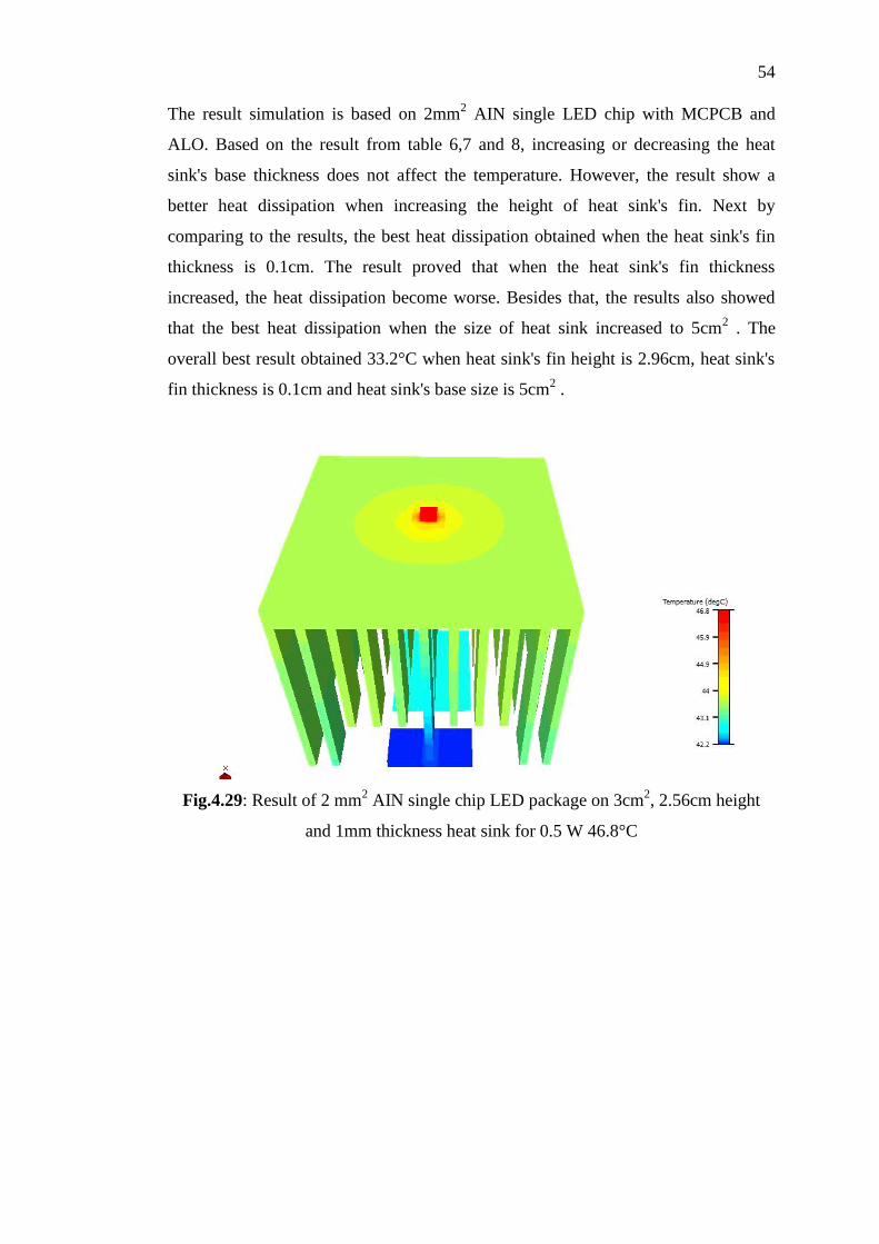
The result simulation is based on 2mm2 AIN single LED chip with MCPCB and
ALO. Based on the result from table 6,7 and 8, increasing or decreasing the heat
sink's base thickness does not affect the temperature. However, the result show a
better heat dissipation when increasing the height of heat sink's fin. Next by
comparing to the results, the best heat dissipation obtained when the heat sink's fin
thickness is 0.1cm. The result proved that when the heat sink's fin thickness
increased, the heat dissipation become worse. Besides that, the results also showed
that the best heat dissipation when the size of heat sink increased to 5cm2 . The
overall best result obtained 33.2°C when heat sink's fin height is 2.96cm, heat sink's
fin thickness is 0.1cm and heat sink's base size is 5cm2 .
Fig.4.29: Result of 2 mm2 AIN single chip LED package on 3cm
2, 2.56cm height
and 1mm thickness heat sink for 0.5 W 46.8°C

55
Fig.4.30: Result of 2 mm2 AIN single chip LED package on 3cm
2, 2.76cm height
and 1mm thickness heat sink for 0.5 W 46.1°C
Fig.4.31: Result of 2 mm2 AIN single chip LED package on 3cm
2, 2.96cm height
and 1mm thickness heat sink for 0.5 W 46.6°C

56
Fig.4.32: Result of 2 mm2 AIN single chip LED package on 4cm
2, 2.56cm height
and 1mm thickness heat sink for 0.5 W 34.2°C
Fig.4.33: Result of 2 mm2 AIN single chip LED package on 4cm
2, 2.76cm height
and 1mm thickness heat sink for 0.5 W 33.9°C

57
Fig.4.34: Result of 2 mm2 AIN single chip LED package on 4cm
2, 2.96cm height
and 1mm thickness heat sink for 0.5 W 33.5°C
Fig.4.35: Result of 2 mm2 AIN single chip LED package on 5cm
2, 2.56cm height
and 1mm thickness heat sink for 0.5 W 34.6°C

58
Fig.4.36: Result of 2 mm2 AIN single chip LED package on 5cm
2, 2.76cm height
and 1mm thickness heat sink for 0.5 W 34.1°C
Fig.4.37: Result of 2 mm2 AIN single chip LED package on 5cm
2, 2.96cm height
and 1mm thickness heat sink for 0.5 W 33.2°C

59
CHAPTER 5
5 CONCLUSION AND RECOMMENDATIONS
5.1 Conclusion
From the research, there are mainly focused on two parts which are LED design and
heat sink design. Based on both designs, a parametric studies done to investigate the
cooling and heating process of LED modeling.
For the LED design, the simulation result shows that PCB materials FR-4
thermal conductivity of 0.3W/m.K and MCPCB thermal conductivity of 201W/m.K.
MCPCB material is the most effective solution for thermal conductivity where FR-4
return 130°C which is incompatible for industrial use because exceeded optimum
operating temperature of 90°C while MCPCB return 34.8°C for total power 0.5Watt,
single 1mm x 1mm GaN LED chip and ALO TIM material. Therefore, the material
of FR-4 for PCB omitted.
.
Next, comparison of simulation results for three types of LED chip material
for InGaN/GaN, GaP and AIN. For InGaN/GaN material of thermal conductivity of
130 W/m.K, the maximum temperature yield 34.8°C; For GaP material of thermal
conductivity of 110 W/m.K, the maximum temperature yield 34.9°C; For AIN
material of thermal conductivity of 285 W/m.K, the maximum temperature yield
34.5°C. Thus, AIN is the best material to be used for develop LED chip.
Other than that, among all the Thermal interface materials of grease, ALO,
film and tape, ALO is out perform than other materials by 34.8°C while grease

60
achieved 36.6°C, film achieved 38.7°C and tape achieved 47.7°C. Thus, ALO proved
to have better thermal conductivity for heat dissipation, therefore ALO is the best
material to be used for develop TIM.
For single chip LED by changing total power in range of 0.5 W to 1 W with
LED chip sizes; 1.5mm2 and 2mm
2 yield a similar result by 33.9°C and 33.7°C for
0.5 W while 42.7°C and 42.4°C for 1 W. For 2 chip LED by changing total power in
range of 1 W to 2 W; 1.5mm2 and 2mm
2 yield a same result by 41°C for 1 W and
55.5°C for 2 W. For 4 chip LED by changing total power in range of 2 W to 4 W,
1.5mm2 and 2mm
2 yield a same result by 53.4°C for 2 W and 77.4°C for 4 W. This
proved that 1.5mm2 and 2mm
2 yield the best result compared to 1mm
2; Other than
that, the overall simulation results is acceptable since the maximum operating
junction temperature yield 78.5°C which is under 90°C.
For heat sink design, a combinations of sizes of heat sink, heat sink's fin
thickness and height and heat sink's base thickness done for parametric studies. From
the result and placement of LED chip on heat sink also play an important role for
heat dissipation. The best result obtained when LED chip placed exactly closed to the
fin of heat sink. Base size of the heat sink is one of the factor that influence the
operating junction temperature, compared to the base sizes of 3cm2 to 5cm
2 by fin
height of 2.96cm and fin thickness 1mm, each yield 46.6°C, 33.6°C and 33.2°C.
5cm2 yield the better result of 33.2°C while 4cm
2 's result is acceptable since both
result is similar.
Next, heat sink's base thickness does not affect much to operating junction
temperature however heat sink's fin thickness and fin height does make difference to
the temperature. For fin thickness 1mm to 2mm, fin thickness of 1mm yield better
thermal dissipation; For fin height of 2.56cm to 2.96cm, fin height of 2.96cm yield
the better thermal dissipation. Therefore, combination of heat sink's base size of
5cm2, fin thickness of 1mm and fin height of 2.96cm yield the best result of 33.2°C
among all the results.
61
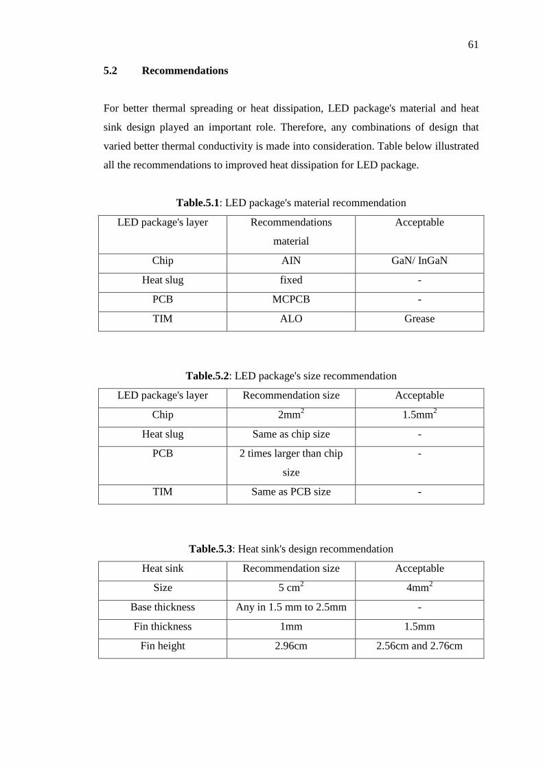
5.2 Recommendations
For better thermal spreading or heat dissipation, LED package's material and heat
sink design played an important role. Therefore, any combinations of design that
varied better thermal conductivity is made into consideration. Table below illustrated
all the recommendations to improved heat dissipation for LED package.
Table.5.1: LED package's material recommendation
LED package's layer Recommendations
material
Acceptable
Chip AIN GaN/ InGaN
Heat slug fixed -
PCB MCPCB -
TIM ALO Grease
Table.5.2: LED package's size recommendation
LED package's layer Recommendation size Acceptable
Chip 2mm2 1.5mm
2
Heat slug Same as chip size -
PCB 2 times larger than chip
size
-
TIM Same as PCB size -
Table.5.3: Heat sink's design recommendation
Heat sink Recommendation size Acceptable
Size 5 cm2 4mm
2
Base thickness Any in 1.5 mm to 2.5mm -
Fin thickness 1mm 1.5mm
Fin height 2.96cm 2.56cm and 2.76cm

62
REFERENCES
Barb Schmitz 2015, Simulation Reduces the Complexities of LED Design.
http://www.3dcadworld.com/cfd-simulation-reduces-complexities-led-design/
R. Sam Sukumar et al. 2013, International Journal of Engineering Research and
Applications (IJERA) ISSN: 2248-9622 Vol. 3, Issue 2, March -April,
pp.1557-1561.
Gavin Sullivan & Campbell Edmondson 2008, 'Heat and Temperature' Continuing
Education in Anaesthesia, Critical Care & Pain, Vol. 8 No.3.
Oon Siang Ling 2010, 'Thermal Modeling of High Power LEDs', AV02-2391EN -
March 20.
Sridhar Narasimhan et al. 2003, 'Thermal Compact Modeling of Parallel Plate Heat
Sinks', IEEE Trans. Comp, March, Vol.26, No.1.
Kevin R. Anderson 2013, 'STAR CCM+ CFD Simulations of Enhanced Heat
Transfer in High-Power Density Electronics Using Forced Air Heat
Exchanger and Pumped Fluid Loop Cold Plate Fabricated from High Thermal
Conductivity Materials', Journal of Electronics Cooling and Thermal
Control, December, pp. 144-154.
http://dx.doi.org/10.4236/jectc.2013.34016
Linton R.L et al. 1995, 'Coarse and Detailed CFD Modeling of a Finned Heat Sink',
IEEE Trans. on Comp, Packaging and Manufacturing Tech—Part A, Vol.18,
No.3.
Al Ashry M.H.S. 2015, 'Augmenting the Heat Sink for Better Heat Dissipation'.
Circuits and Systems, February Vol. 6, pp. 21-29.
http://dx.doi.org/10.4236/cs.2015.6200315
Dong Mei Li 2009, 'Numerical Simulation on Heat Pipe for High Power LED Multi-
Chip Module Packaging', Electronic Packaging Technology & High Density
Packaging. ICEPT-HDP '09. International Conference on 10-13 Aug, E-
ISBN : 978-1-4244-4659-9.
Tsai Bor Jang 2011, 'Thermal analysis of a high power LED multi-chip package
module', INTERNATIONAL JOURNAL OF ENERGY, Vol. 5, Issue 4.

63
Yan Lai et al. 2006, 'Thermal Management of Bright LEDs for Automotive
Applications', Thermal, Mechanical and Multiphysics Simulation and
Experiments in Micro-Electronics and Micro-Systems. 7th International
Conference on 24-26 April, Print ISBN: 1-4244-0275-1.
András Poppe 2008, 'ELECTRICAL, THERMAL AND OPTICAL
CHARACTERIZATION OF POWER LED ASSEMBLIES', ISBN: 2-
916187-04-9.
G. Farkas et al. 2004, 'Electric and thermal transient effects in high power optical
devices' In proceedings of the 20th IEEE SEMITHERM Symposium, 9-11
March, San Jose, CA, USA, pp. 168-176.
Kai Lin Pan 2014, 'Study on the Thermal Resistance of Multi-chip Module High
Power LED Packaging Heat Dissipation System', Sensors & Transducers,
October 2014 Vol. 180, Issue 10, pp. 72-79.
Szekely 1991, 'Circuits and Systems', IEEE Transactions on July, Vol. 38, Issue 7
Cheng et al. 2010, 'Study of heat transfer through layers of textiles using finite
element method', International Journal of Clothing Science and Technology,
Vol. 22, Issue 2/3, pp.161 - 173.
R.L. Panton 1996, 'Incompressible flow', second ed., Wiley-Interscience.