modeling of threading dislocation reduction in growing gan layers
TRANSCRIPT

Journal of Crystal Growth 231 (2001) 371–390
Modeling of threading dislocation reduction in growingGaN layers
S.K. Mathisa,1, A.E. Romanovb, L.F. Chena, G.E. Beltzc, W. Pomped, J.S. Specka,*aMaterials Department, University of California, Santa Barbara, CA 93106, USA
bA.F. Ioffe Physico-Technical Institute, Russian Academy of Sciences, 194021 St. Petersburg, RussiacMechanical Engineering Department, University of California, Santa Barbara, CA 93106, USA
d Institut f .ur Werkstoffwissenschaft, Technische Universtit .at Dresden, Hallwachsstr. 3, 01069 Dresden, Germany
Abstract
In this work, a model is developed to treat threading dislocation (TD) reduction in (0 0 0 1) wurtzite epitaxial GaNthin films. The model is based on an approach originally proposed for (0 0 1) FCC thin film growth and uses theconcepts of mutual TD motion and reactions. We show that the experimentally observed slow TD reduction in GaN
can be explained by low TD reaction probabilities due to TD line directions practically normal to the film surface. Thebehavior of screw dislocations in III-nitride films is considered and is found to strongly impact TD reduction.Dislocation reduction data in hydride vapor phase epitaxy (HVPE) grown GaN are well described by this model. The
model provides an explanation for the non-saturating TD density in thick GaN films. r 2001 Elsevier Science B.V. Allrights reserved.
Keywords: A1. Line defects; A3. Hydride vapor phase epitaxy; A3. Metalorganic chemical vapor deposition; B1. Nitrides
1. Introduction
Gallium nitride based semiconducting materials grown directly on available substrates have highdislocation densities. Extended defects such as dislocations and stacking faults are known to have a reducedeffect on device operation in GaN, but at sufficiently high densities, threading dislocations (TDs) adverselyaffect device properties. For example, at TD densities above about 5� 109 cm�2, non-radiativerecombination at dislocations limits light emitting diode efficiencies [1,2]. TDs also act as chargedscattering centers and reduce carrier mobilities [3]. Leakage current in reverse-biased p–n junctions isreduced when TD densities are decreased [4]. In nitride-based semiconductors, TDs themselves are notmobile during device operation [5], but they have been shown to act as a fast diffusion pathway for Mgdopants [6]. Thus, threading dislocations densities in the range of 1� 108–1� 1010 cm�2 in GaN may
*Corresponding author. Tel.: +1-805-893-8005; fax: +1-805-893-8983.
E-mail address: [email protected] (J.S. Speck).1Current address: Agilent Technologies, 350 West Trimble Road, MS 90UB, San Jose, CA 95131-1008, USA.
0022-0248/01/$ - see front matter r 2001 Elsevier Science B.V. All rights reserved.
PII: S 0 0 2 2 - 0 2 4 8 ( 0 1 ) 0 1 4 6 8 - 3

ultimately limit device applications, even with a short minority carrier diffusion length on the order of50 nm.The conventional method of reducing TD density in semiconductor films uses either graded or constant
composition buffer layers. This method has had success in reducing TD densities in cubic semiconductorsystems such as SiGe/Si or InGaAs/GaAs [7,8]. In growing (0 0 1) zincblende semiconductor films,dislocations lie on inclined (1 1 1) slip planes. As growth proceeds, they can meet each other and react,lowering the TD density. It was demonstrated that TD density in constant composition FCCsemiconductor buffer layers depends on layer thickness (h) as 1=h [9]. The situation is different in thenitride semiconductors, which have the hexagonal wurtzite structure. Experimentally, the line directions ofthe majority of TDs were observed to be normal to the film/substrate interface and parallel to the [0 0 0 1]direction [10]. Detailed analyses demonstrate that the majority of these TDs are edge (Burgers vectorb ¼ /1 1 %2 0S) dislocations and some screw (b=/0 0 0 1S) dislocations [11]. We will show that the mixeddislocations (b ¼ 1
3/1 1%2 3S) are inclined at approximately 121 to the film normal. For this reason (and we
will demonstrate this in our calculations), buffer layers have had limited success in reducing TD densities inGaN. In a recent study using hydride vapor phase epitaxy (HVPE), a dislocation density of low to mid-106 cm�2 was observed after 300 mm of growth [12]. This represents a large reduction in TD densitycompared with the B109–1010 cm�2 typically observed in 1–5 mm thick films.GaN has a high mismatch with the substrates on which it is generally grown, sapphire and SiC. In the
case of GaN on sapphire, the lattice parameter mismatch isB14.6% [11]. GaN films on sapphire are grownin MOCVD using a standard two-step process. Prior to the first growth step, the sapphire substrate isheated to high temperature (HT, 1000–11001C) and cleaned with flowing hydrogen (B5–30min). Then,while maintaining high temperature, the sapphire substrate may then be exposed to ammonia(prenitridation). The substrate temperature is then reduced to typically 500–6001C (LT) and a nucleationlayer is grown with a nominal thickness of B200 (A. The nucleation layer (NL) structure is composed ofthree dimensional facetted, predominantly cubic (1 1 1) oriented GaN grains. Adjacent NL grains onlycontact one another at their base, which has been attributed to the high energy necessary to coalesce islandswith a large degree of stacking disorder. After the NL growth, the film is heated to the normal growthtemperature of 10501C and the cubic GaN NL partially transforms to hexagonal GaN. Larger (B1 mm) sizeislands (‘HT islands’) nucleate on the LT layer. Isolated HT islands laterally overgrow the nucleation layerwithout generating any threading dislocations. Rather, all disorder between the NL islands and individualHT islands is accommodated by Shockley and Frank partial dislocations with line directions in the (0 0 0 1)plane, or by local strain. The threading dislocations are generated as a result of coalescence of adjacent HTislands. Rotation about the [0 0 0 1] direction leads to pure tilt boundaries and rotation about directions[uvt0] results in vertical twist boundaries. Thus, the majority of threading dislocations in GaN, grown underoptimized conditions, result from coalescence of HT islands. Typical TD densities are in the range mid-108–mid-109 cm�2 using this method. It is possible to extensively prenitride the sapphire at HT. This generallyresults in a highly columnar microstructure consisting of only pure edge TDs arranged in tilt boundarieswith a density in the low 1010 cm�2-range.The aim of the present work is to understand the TD reduction mechanism in GaN films and to explain
the weaker TD density reduction in comparison with cubic semiconductor buffer layers. This is done byadapting a prior model for TD density falloff in FCC thin films to the case of [0 0 0 1] oriented hexagonalsemiconductors [9,13]. First, experimental observations of TD types (screw, edge, and mixed dislocations)and densities are considered. The possible dislocation reactions, such as fusion or annihilation, aredetermined for each of the 20 possible threading dislocations in GaN. Relative probabilities are determinedfor each of these reactions based on crystallographic considerations. Coupled differential equations are usedto model the TD density evolution with changing film thickness. Using experimental observations, themodel’s validity is evaluated. Finally, implications of the model for screw dislocation behavior areconsidered. The connection between growth initiation conditions and TD density falloff in GaN is discussed.
S.K. Mathis et al. / Journal of Crystal Growth 231 (2001) 371–390372
2. Background
2.1. Types of TDs in GaN
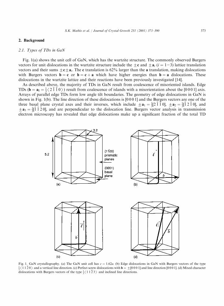
Fig. 1(a) shows the unit cell of GaN, which has the wurtzite structure. The commonly observed Burgersvectors for unit dislocations in the wurtzite structure include the 7c and 7ai (i ¼ 123) lattice translationvectors and their sums 7c7ai: The c translation is 62% larger than the a translation, making dislocationswith Burgers vectors b ¼ c or b ¼ cþ a which have higher energies than b ¼ a dislocations. Thesedislocations in the wurtzite lattice and their reactions have been previously investigated [14].As described above, the majority of TDs in GaN result from coalescence of misoriented islands. Edge
TDs (b ¼ aI ¼ 13/2
%1 %1 0S) result from coalescence of islands with a misorientation about the [0 0 0 1] axis.Arrays of parallel edge TDs form low angle tilt boundaries. The geometry of edge dislocations in GaN isshown in Fig. 1(b). The line direction of these dislocations is [0 0 0 1] and the Burgers vectors are one of thethree basal plane crystal axes and their inverses, which include 7a1 ¼ 1
3½2%1 %1 0�; 7a2 ¼ 1
3½%1 2 %1 0�; and
7a3 ¼ 13½%1 %1 2 0�; and are perpendicular to the dislocation line. Burgers vector analysis in transmission
electron microscopy has revealed that edge dislocations make up a significant fraction of the total TD
Fig. 1. GaN crystallography. (a) The GaN unit cell has c ¼ 1:62a: (b) Edge dislocations in GaN with Burgers vectors of the type13/1 1
%2 0S and a vertical line direction. (c) Perfect screw dislocations with b ¼ 7½0 0 0 1� and line direction [0 0 0 1]. (d) Mixed character
dislocations with Burgers vectors of the type 13/1 1
%2 3S and inclined line directions.
S.K. Mathis et al. / Journal of Crystal Growth 231 (2001) 371–390 373

density in high-quality MOCVD films [11,15]. Additionally, it appears that the edge character dislocationsrepresent a larger fraction of the total TD density in thicker films. Wu et al. examined both 1 and 5 mm thickfilms grown under identical conditions and showed that the edge TDs make up 40% of the total TD densityin 1 mm thick MOCVD-grown films, while after 5 mm of growth, they make up 70% of all TDs [11].Pure screw dislocations are the most uncommon type of TD in GaN films. Both their line direction and
Burgers vector lie along the [0 0 0 1] direction, as shown schematically in Fig. 1(c). Published TEMmeasurements usually put screw dislocations at o1 to 10% of the overall TD density in MOCVD-grownmaterial [16]. Wu et al. reported that pure screw TDs had a very small proportion (much less than 1%) ofthe total TD density in MOCVD-grown GaN [11]. However, it has been reported that in MBE-initiatedGaN growth on sapphire, screw dislocations have been found to represent 20% of the overall TD density[15]. Nanopipes, which are sometimes observed in GaN films grown on SiC and on sapphire, have beenassociated with open-core screw dislocations [17]. Nanopipes are surrounded by growth spirals at the filmsurface, indicating a c-component Burgers vector dislocation at their centers [17]. However, nanopipesappear not to have appreciable density in high-quality material, and often screw dislocations have closedcores [16]. It is not presently understood why open core dislocations occur, or why screw dislocations havelow density in epitaxial GaN films [18].Burgers vectors for mixed dislocations are b ¼ cþ ai ¼ 1
3/1 1%2 3S: The reported fraction of mixed
dislocations varies from 2% of the total density in the case of MBE-initiated growth to 68% inmetalorganic vapor phase epitaxy-grown (MOVPE-grown) material [15,16]. As mixed dislocations are theonly TDs with an (energetically favored) inclined line direction relative to the film normal (this point will bedeveloped below), they are the only TDs moving laterally relative to other TDs during growth. Thegeometry of a mixed dislocation is shown in Fig. 1(d). As we will show, they drive TD reduction by reactingwith other dislocations. The microstructure of a 1.4 mm-thick MBE-grown film on a 1.6 mm-thick MOCVDlayer of GaN on sapphire is shown in Fig. 2. Growth conditions for this sample are described in Ref. [19].This cross-section TEM picture was imaged in the g ¼ 0 0 0 2 diffraction condition, under which onlydislocations with screw character are visible. Since the proportion of pure screw (b ¼ c) dislocations is verylow, essentially all of the dislocations imaged are mixed-character (b ¼ aþ c) dislocations. We assume thatthe maximum angle between the surface normal and the dislocation line direction will be the true angle of
Fig. 2. Cross-section TEM micrograph of 1.4 mm MBE-grown GaN on a 1.6 mm MOCVD-grown GaN buffer. Micrograph taken
under g ¼ 0 0 0 2 imaging condition. Under this imaging condition, only dislocations with a c-component Burgers vector are visible.
Due to the low screw TD density, the dislocations are predominantly of mixed screw-edge character with line direction inclined at
B12.21 to the surface normal. This angle was determined by taking the maximum inclination angle at sufficient distance from the film/
substrate interface so that TD generation conditions did not dictate line direction. The maximum inclination was used because TDs
lying in the plane normal to the viewing direction would have the largest apparent inclination, while those aligned with the viewing
direction or at an angle o901 would have a smaller apparent inclination.
S.K. Mathis et al. / Journal of Crystal Growth 231 (2001) 371–390374

deviation, as only one slip plane is positioned normal to the viewing direction. This angle was measured tobe approximately 12.21.
2.2. Modeling of TD reduction in FCC semiconductors
Romanov et al. have developed a model for dislocation density evolution in growing films for (0 0 1)oriented FCC materials (see Refs. [9,13]). We adapt the model to the case of GaN hexagonal materials inthis paper, so the essential features of this model are described here. There are 24 unique combinations ofdislocation slip plane and Burgers vector in FCC semiconductors. These consist of four possible {1 1 1} typeslip planes and 6 Burgers vectors (including sign inversions) per slip plane of the type 1/2/1 1 0S.Threading dislocations may result from either island coalescence or stress-driven nucleation processes. Forthe latter case, dislocations are believed to be generated by surface-initiated processes leading to half-loops,with a misfit dislocation and two associated threading segments [20]. Most misfit dislocations in FCCsemiconductors are the so-called 601 dislocations, with Burgers vectors that are inclined at 601 to thedislocation line direction.Fusion or annihilation reactions are the primary mechanisms for TD density reduction in thin films.
Dislocations may react with one another when they are in close proximity. A fusion reaction occurs whentwo TD lines become one TD with the new Burgers vector b3 ¼ b1 þ b2: An annihilation reaction happenswhen two TD lines with opposite Burgers vectors (b1 ¼ �b2) undergo the reaction b1 þ b2 ¼0; removing thedislocations entirely. The similar reactions specific to GaN films will be considered in detail in the followingsections.Dislocations may meet and react with increasing film thickness. TDs do not experience misfit stress-
induced motion in a relaxed layer, but rather their relative motion is due to their inclined line directions. Asthe film thickness increases, the point of intersection of inclined TDs with the surface moves laterally. Whenone TD interacts with another TD in FCC semiconductors, it has a 1 in 24 chance of an annihilationreaction and a 6 in 24 chance for a fusion reaction. For each TD family, a differential equation was writtenthat represents the density evolution with thickness. The resulting 24 coupled differential equations werethen solved numerically.The overall TD density r can also be described by a simplified equation [21]
dr ¼ �Kr2 dh; ð1Þ
where K is considered to be a dislocation reaction cross-section (kinetic reaction coefficient). K isproportional to the dislocation annihilation radius rA; but also is a function of the analogous dislocationfusion reaction radius rF when fusion reactions are included. In these calculations, K is assumed to beindependent of thickness. The initial condition for this equation is a known TD density rðh ¼ h0Þ ¼ r0 atsome thickness h0: The solution of Eq. (1) is given as
r ¼1=K
hþ #h; ð2Þ
where the parameter #h corresponds to the initial threading dislocation density and is defined by the relation
#h ¼ ðKr0Þ�1 � h0: ð3Þ
For TDs to react, they must come within a reaction distance rI of one another, where rI ¼ rA or rF: Thereaction distance rI is governed by the type of material (the Peierls barrier) and the temperature. Thisdistance (annihilation or fusion radius) has been previously estimated to be between 500 and 5000 (A in FCCsemiconductors [9]. Recently, calculations have confirmed this range of annihilation radii [22]. Fromexperimental data, rA has been evaluated to beB1000 (A in GaAs films at the ordinary growth temperature(5801C) [23].
S.K. Mathis et al. / Journal of Crystal Growth 231 (2001) 371–390 375
The results of this TD reduction model reproduce the experimentally observed B1=h dependency of TDdensity on thickness at large h: Compared with GaN, TDs in FCC semiconductors are always reduced morequickly with increasing film thickness due to their inclined line directions.
3. Dislocation reduction model for GaN
3.1. Dislocation reactions
There are 20 unique types of dislocations in GaNFeach defined by their Burgers vector and linedirection. For example, there are two different types of screw dislocations, with Burgers vector b ¼7½0 0 0 1�: Additionally, six different edge dislocations and 12 different mixed character dislocations exist inthe nitrides. The driving force for TD reactions is the minimization of film free energy. The line energy ofthe dislocation is proportional to b2; so the criterion for successful TD reactions is
b21 þ b22Xb23: ð4Þ
This is the ‘b2-criterion’ [21]. The reaction is still driven to completion if the left and right hand terms ofEq. (4) are equal since this removes one dislocation line, thereby reducing the overall energy (removal ofone TD core). Each of the 20 possible TD types is listed in Table 1 with its reactions and TDs producedthrough the reaction, if any. Several of these reactions produce compound Burgers vector dislocations. Forexample, the following reaction is energetically favored
ða3 � cÞ þ ð�a2 þ cÞ-ða3 � a2Þ ð5Þ
since the b2 criterion is satisfied. However, the reaction will continue with another step:
ða3 � a2Þ-ða3Þ þ ð�a2Þ ð6Þ
to form two separate dislocations, numbers 4 and 5 in Table 1. The reaction in Eq. (6) is energeticallyfavorable according to the b2-criterion. The resulting dislocations will be driven apart from one anotherbecause there is an angle of 601 between a3 and �a2. There are several such compound reactions in thissystem, which are driven primarily by the large reduction in strain energy due to the removal of the ccomponent of the Burgers vector in mixed dislocations. We note that ‘two-to-two’ compound reactions arenot predicted for FCC (0 0 1) epitaxy.
3.2. TD line directions
The TD line direction can be determined by minimizing the dislocation energy, which results from acompetition between minimizing the dislocation line length and maximizing the screw character of the TD.We follow here the calculations of line direction performed for the case of a dislocation in (0 0 1) orientedFCC semiconductors as described in Ref. [9]. The core energy is assumed to be independent of thedislocation type in the first approximation for this calculation, but as we will discuss, the screw and edgedislocation core energies may be different. In the isotropic approximation, the elastic strain energy in thelattice surrounding the dislocation is greater for an edge dislocation than for a screw dislocation with thesame length Burgers vector. The dislocation type is determined by the angle f between the Burgers vector band the dislocation line l. A dislocation is pure edge for f ¼ 901 and pure screw for f ¼ 01. The anglesrelevant to the calculation of line direction are shown in Fig. 3. The strain energy depends on f and h:
Eðh;fÞ ¼mb2
4ph
cosðy� fÞcos2fþ
sin2f1� n
� �ln
aRbj j
� �: ð7Þ
S.K. Mathis et al. / Journal of Crystal Growth 231 (2001) 371–390376
Table 1
Reaction table for threading dislocations (TDs) in growing GaN layers. The reactions that are not possible either due to the b2 criterion or for geometric reasons are
indicated with a ‘‘F’’ while reactions that are possible are indicated with their designated number. Reactions that produce two dislocations are denoted with two
numbers corresponding to their products
1 2 3 4 5 6 7 8 9 10 11 12 13 14 15 16 17 18 19 20
a1 �a1 a2 �a2 a3 �a3 a1+c a1�c �a1+c �a1�c a2+c a2�c �a2+c �a2�c a3+c a3�c �a3+c �a3�c c �c
1 a1 F F F F F F F F 19 20 17 18 F F 13 14 F F F F2 �a1 F F F F F F 19 20 F F F F 15 16 F F 11 12 F F3 a2 F F F F F F 17 18 F F F F 19 20 9 10 F F F F4 �a2 F F F F F F F F 15 16 19 20 F F F F 7 8 F F5 a3 F F F F F F 13 14 F F 9 10 F F F F 19 20 F F6 �a3 F F F F F F F F 11 12 F F 7 8 19 20 F F F F7 a1+c F 19 17 F 13 F F 1&1 F A F 6 F 1&4 F 4 F 1&6 F 1
8 a1�c F 20 18 F 14 F 1&1 F A F 6 F 1&4 F 4 F 1&6 F 1 F9 �a1+c 19 F F 15 F 11 F A F 2&2 F 2&3 F 5 F 2&5 F 3 F 2
10 �a1�c 20 F F 16 F 12 A F 2&2 F 2&3 F 5 F 2&5 F 3 F 2 F11 a2+c 17 F F 19 9 F F 6 F 2&3 F 3&3 F A F 2 F 3&6 F 3
12 a2�c 18 F F 20 10 F 6 F 2&3 F 3&3 F A F 2 F 3&6 F 3 F13 �a2+c F 15 19 F F 7 F 1&4 F 5 F A F 4&4 F 4&5 F 1 F 4
14 �a2�c F 16 20 F F 8 1&4 F 5 F A F 4&4 F 4&5 F 1 F 4 F15 a3+c 13 F 9 F F 19 F 4 F 2&5 F 2 F 4&5 F 5&5 F A F 5
16 a3�c 14 F 10 F F 20 4 F 2&5 F 2 F 4&5 F 5&5 F A F 5 F17 �a3+c F 11 F 7 19 F F 1&6 F 3 F 3&6 F 1 F A F 6&6 F 6
18 �a3�c F 12 F 8 20 F 1&6 F 3 F 3&6 F 1 F A F 6&6 F 6 F19 c F F F F F F F 1 F 2 F 3 F 4 F 5 F 6 F F20 �c F F F F F F 1 F 2 F 3 F 4 F 5 F 6 F F F
S.K.Mathisetal./JournalofCrystalGrowth231(2001)371–390
377

Here, m is the shear modulus, n is Poisson’s ratio, R is the screening length for the dislocation energycalculation, and a is chosen to take into account the contribution of the dislocation core. y is the anglebetween b and [0 0 0 1], which is the direction of the shortest possible line length for TDs in (0 0 0 1) GaNfilms. For simplicity we use the isotropic approximation for elastic constants. In calculating the linedirection for a TD at a given thickness, the Burgers vector and film thickness are fixed, so b, h and y areconstant. The energy is then minimized by setting qE=qf ¼ 0 and solving for f: For b ¼ 7ai TDs, f ¼ 901and for b ¼ 7c dislocations, f ¼ 01. That is, the line direction is [0 0 0 1] for both edge and screw TDs,reconfirming experimental observations. For the mixed b ¼ 7ðai7cÞ dislocations, the line direction isinclined to the film normal at y� f ¼ 15:61: This agrees well with the experimental observation of inclinedline directions at y� fE121: Other authors have shown that these line directions may not be accurate forTDs in close proximity to the film/substrate interface [24,25]. However, this work is concerned with the caseof dislocation reduction far from the thickness at which TDs are generated.
3.3. Model equations
From the reaction table, a series of 20 differential equations can be written. They are of the form
dridh
¼ �Xj
Kijrirj þXl
Xm
Klmrlrm: ð8Þ
Here, the ri represent the density of a specific TD family, with number designations given in Table 1. Thefirst summation is for the annihilation and fusion reactions, which reduce the density of the ith family TDsby one per reaction. The second summation is for fusion reactions between other families l and m thatproduce dislocations in the ith family. The Kij are the kinetic coefficients that describe the rate of reactionsbetween dislocations from families i and j:
Kij ¼ 2rI
ffiffiffiffiffiffiffiffiffiffiffiffiffiffiffiffiffiffiffiffiffiffiffiffiffiffi1� ðli nf Þ
2Þq
li nf
½li � ðli nf Þnf �jli � ðli nf Þnf j
�
ffiffiffiffiffiffiffiffiffiffiffiffiffiffiffiffiffiffiffiffiffiffiffiffi1� ðlj nf Þ
2q
lj nf
½lj � ðlj nf Þnf �jlj � ðlj nf Þnf j
������������; ð9Þ
Fig. 3. Angles used in calculation of line direction. f is the angle between the Burgers vector and line direction. y is the angle betweenthe Burgers vector and [0 0 0 1], which is the shortest possible line direction for GaN dislocations in (0 0 0 1) film growth.
S.K. Mathis et al. / Journal of Crystal Growth 231 (2001) 371–390378

where the li are the ith family dislocation line directions and nf is the film normal [9]. In the followingnumerical calculations, we use dimensionless variables by replacing the Kij with *Kij ¼ Kij=2rI and the riwith *ri ¼ rijr
2I : For simplicity, we took rA to be constant for all reactions and rF ¼ rA in this model. In this
calculation, the reaction probability depends solely on the line direction of the dislocations and not on theslip planes of the TDs. In fact, this is a simplification as each dislocation has a distinct line direction/Burgers vector combination and therefore a different Peierls barrier to dislocation motion. It has also beenassumed that the TDs may move out of their slip planes due to elevated growth temperatures and proximityto the surface of the sample, which is a source and sink for point defects. This non-conservative motionallows only the distance between the TDs, and not the slip planes on which they lie, to dictate the reactionrate for any pair of TDs. The full system of coupled differential equations is included in Appendix A. Thecalculated coefficients *Kij ¼ Kij=2rI are included in Appendix B.
4. Results of numerical solutions
4.1. Allowed dislocation reactions and initial conditions
There have been few direct observations of screw dislocation behavior in GaN, so we assume threeconditions for GaN screw TDs in the model. (1) In the first case, screw dislocations are assumed to behavein the same way as edge and mixed dislocations; they react with other dislocations and are produced byreactions between other dislocation pairs. (2) The second case assumes that screw dislocations are notcapable of reacting with other dislocations. This might happen, for example, if the screw dislocation existsat the center of a growth hillock or at the center of a nanopipe. In the case of a growth hillock, mixeddislocations must elongate and move across the hillock to reach the screw dislocation, making reaction lesslikely. Open core dislocation motion requires mass transport. Thus, reactions involving screw dislocationscould be less likely. Additionally, dislocation reactions that produce screw dislocations might also be lesslikely if their core energy is large, since the production of a screw dislocation would be energetically costly.The core structure of screw dislocations is different from that of mixed or edge-type dislocations since thecore bonds are not broken, but highly stretched. (3) The third condition investigated was an elevatedreactivity for screw dislocations. This would lead to a lower screw dislocation density since the screwdislocations would have a larger annihilation radius (for example due to cross-slip) and would be rapidlyreduced through reaction.The six initial conditions used in these calculations are summarized in Table 2. Cases 1 and 3 have 70%
edge dislocations and 30% mixed dislocations. These proportions were reported for MOCVD-grownmaterial [26]. Cases 2, 4 and 6 had density distributions given as 60% edge, 30% mixed, and 10% screw.These cases were taken for comparison between low- and high-screw TD density material. Finally, Case 5was initially given a much higher proportion of mixed character TDs, with 30% edge and 70% mixeddislocations. This was done to compare high mixed TD content and high edge TD content films. In themodeling, the total initial density was set at 1� 1010 cm�2 for all cases and the initial density distribution issummarized in Table 2. Neither the Peierls stress nor the annihilation radius has been estimated for GaN,thus we assume an annihilation radius of 500 (A for ordinary growth conditions. We assume that theannihilation radius in GaN will be smaller than that in GaAs due to the generally higher Peierls stresses inhexagonal materials. Later, we will show that this value is consistent with the experimental data. Within themodel, this corresponds to a dimensionless initial TD density of *ri1 ¼ 0:25: The initial density of eachfamily of dislocations (unique Burgers vector) was calculated by first dividing the density between the threetypes of TDs (screw, edge, and mixed), and then dividing the density evenly between the families within thatdislocation type. For example, Case 1 would have 30% of the total TD density as mixed dislocations, and
S.K. Mathis et al. / Journal of Crystal Growth 231 (2001) 371–390 379

that density would then be evenly divided among the twelve mixed TD families. The 20 coupled differentialequations were then solved numerically. For Cases 3, 4, and 6, the calculation included all reactions thatwere determined to be energetically possible from the b2-criterion. Case 6 was given an increasedprobability of screw TD reaction by increasing the reaction radius by one order of magnitude for reactionsinvolving screw TDs. Cases 1, 2 and 5 excluded the possibility of screw dislocations reacting with otherdislocations or being formed by reactions between edge and mixed dislocations (the reaction cross-sectionsKij were zero for reactions involving screw dislocations for Cases 1, 2 and 5).
4.2. Solutions for TD densities
4.2.1. Overall comparison of Cases 1 to 6Fig. 4(a) shows the dislocation density evolution with thickness for Cases 1, 2, 3 and 4. In each of the
following figures, the normalized TD density ( *rTD ¼ rTD r2A) is plotted against the normalized thickness( *h ¼ h=rA). The TD density for Cases 3 and 4 reduces initially with increasing thickness, but reaches asaturation value. The TD density for Cases 1 and 2, by contrast, continues to reduce with increasingthickness. Case 1, which has no initial screw TD density and no screw TDs formed by reaction withthickness, has the lowest final TD density after a thickness of h=rA ¼ 1000 mm/500 (A=20 000 (normalizedthickness). In Fig. 4(b), a curve fit to the results of Case 1 shows that the data are well described by therelation
rTD ¼1
Kh2=3 þ #h: ð10Þ
From the curve fit, the normalized values for K and #h are 0.057 and 3.70, respectively. The origin of thisdependence on h�2=3 is not understood at present and is a topic of ongoing investigation.Lower initial screw TD density leads to a lower final TD density. For example, Case 1 has an initial screw
TD density of zero, and when compared to Case 2 (which had the same reaction conditions), the final TD
Table 2
Threading dislocation cases used in calculations. Cases 1–6 are summarized, with initial edge, mixed, and screw subdensities and screw
dislocation behavior
Subdensity (%) Screw dislocation behavior
Edge Mixed Screw (Generation is screw formation at coalescence, reactions refer to screw as reactants or products)
1 70 30 0 r0s ¼ rsðhÞ ¼ 0
Screw generation and reaction prohibited
2 60 30 10 r0s ¼ rsðhÞa0
Screw generation allowed, reaction prohibited
3 70 30 0 r0s ¼ 0arsðhÞScrew generation prohibited, reaction allowed
4 60 30 10 r0sa0arsðhÞScrew generation and reaction allowed
5A 30 70 0 r0s ¼ rsðhÞ ¼ 0
Screw generation and reaction prohibited, high mixed TD density and low edge TD density
5B 98 2 0 r0s ¼ rsðhÞ ¼ 0
Screw generation and reaction prohibited, high mixed TD density and low edge TD density
6 60 30 10 r0sa0arsðhÞ10� higher annihilation radius for screw TDs
S.K. Mathis et al. / Journal of Crystal Growth 231 (2001) 371–390380

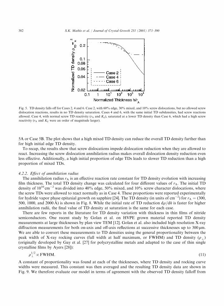
density is lower for Case 1. This is to be expected, as in both Cases 1 and 2, no screw TD reactions areallowed, and therefore, the screw TDs are not removed in Case 2. Cases 3 and 4, which did have screw TDreactions included, show a similar trend: an initial screw TD density leaves a higher final TD density forCase 4.High, low, and normal screw dislocation annihilation radius cases are shown in Fig. 5. When screw TDs
are not allowed to react, as in Case 2, the lowest final TD density is reached since there is no saturation ofthe total TD density. Case 4, which has screw TDs with the calculated reactivity Kij (normal annihilationradius), initially reduces TD density more slowly than Case 6, which has screw dislocations with 10� rAand therefore 10� Kij : However, the TD density for Case 6 saturates sooner with thickness and at a higherTD density than Case 4. The reason is that faster reactions between screw and mixed TDs result in fewermixed TDs available for reaction with edge TDs. Therefore, all TDs are vertical after the mixed TD contentis depleted and no further reactions are possible.The subdensity evolution of edge, mixed, and screw-type dislocations are shown in Fig. 6. Case 2, with no
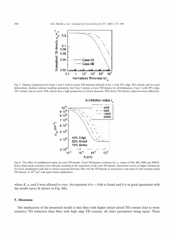
screw dislocation reactions, is shown in Fig. 6(a). The screw TD density remains constant with thickness,while the edge and mixed TD content falls without saturation. For Case 4, shown in Fig. 6(b), the initial TDsubdensities are the same as for Case 2. However, the TD reactions involving screw dislocations are allowedin this case. The result is that mixed TD content falls more quickly with thickness than for Case 2. This isdue to both the screw-mixed reactions producing vertical edge dislocations, and the edge-mixed reactionsproducing vertical screw dislocations. As a result, the mixed TD density becomes so low as to preventfurther interaction among TDs, with the end result a saturation in TD density. Fig. 6(c) shows thesubdensities for Case 6, where the screw TDs are more reactive than Cases 1–5. Although both screw andedge TD densities decrease, the mixed dislocations are depleted quickly with thickness as in Case 4, and theTD density saturates.Cases 5A and 5B are shown together in Fig. 7. In both cases, screw TD reactions were not allowed. Case
5A, with high mixed TD density (70% mixed and 30% edge TDs), attains a lower TD density overall thanCase 5B. Case 5B has 98% edge TDs and 2% mixed TDs. The TD density does not saturate in either Case
Fig. 4. Total TD density evolution with film thickness for Cases 1–4. (a) Cases 1 and 2, with no screw dislocation reactions allowed, do
not display saturation behavior. Cases 3 and 4, with screw dislocation reactions allowed, reach a minimum TD density and saturate.
Case 2, with an initial screw TD subdensity of 10% of the total TD density, has a higher final TD density than that of Case 1, which
had no screw TDs. Similarly, Case 4, with an initial non-zero screw subdensity, saturated at a higher TD density than Case 3.
Maximum thickness corresponds to 250mm for an annihilation radius of rA ¼ 500 (A. (b) A curve fit of Case 1 shows that TD density
depends on 1=h2=3 for large h. The best fit was found with rTDr2A ¼ 1=½0:057ðh=rAÞ
2=3 þ 3:70�:
S.K. Mathis et al. / Journal of Crystal Growth 231 (2001) 371–390 381
5A or Case 5B. The plot shows that a high mixed TD density can reduce the overall TD density further thanfor high initial edge TD density.To recap, the results show that screw dislocations impede dislocation reduction when they are allowed to
react. Increasing the screw dislocation annihilation radius makes overall dislocation density reduction evenless effective. Additionally, a high initial proportion of edge TDs leads to slower TD reduction than a highproportion of mixed TDs.
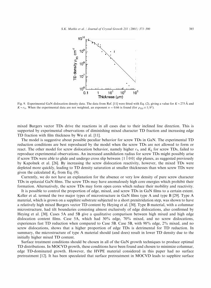
4.2.2. Effect of annihilation radiusThe annihilation radius rA is an effective reaction rate constant for TD density evolution with increasing
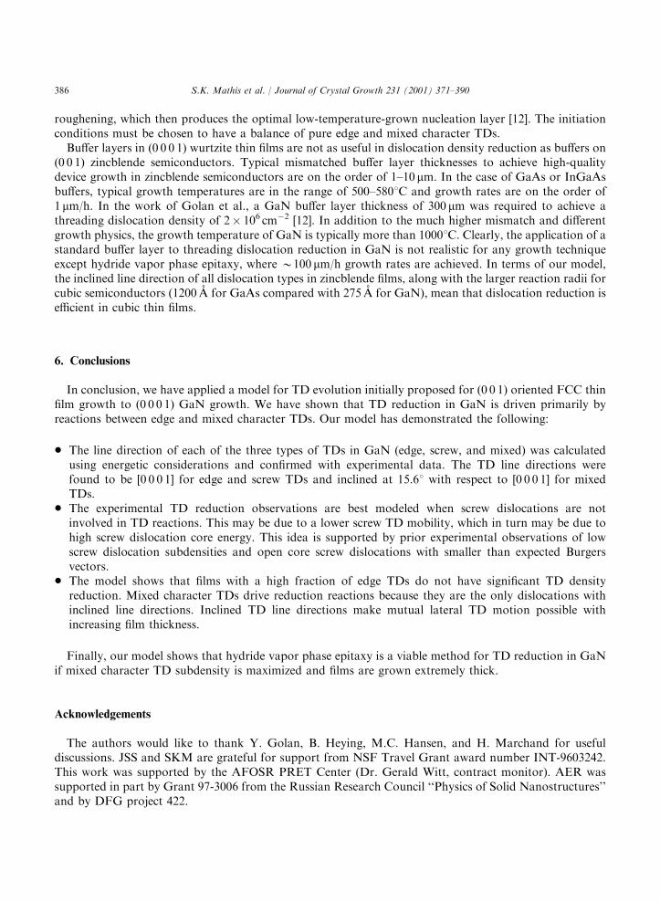
film thickness. The total TD density change was calculated for four different values of rA: The initial TDdensity of 1010 cm�2 was divided into 40% edge, 50% mixed, and 10% screw character dislocations, wherethe screw TDs were allowed to react normally as in Case 4. These proportions were reported experimentallyfor hydride vapor phase epitaxial growth on sapphire [24]. The TD density (in units of cm�2) for rA ¼ ð300;500, 1000, and 2000 (A) is shown in Fig. 8. While the initial rate of TD reduction dr=dh is faster for higherannihilation radii, the final value of TD density at saturation is the same for each case.There are few reports in the literature for TD density variation with thickness in thin films of nitride
semiconductors. One recent study by Golan et al. on HVPE grown material reported TD densitymeasurements at large thicknesses by plan view TEM [12]. Golan et al. also included high resolution X-raydiffraction measurements for both on-axis and off-axis reflections at successive thicknesses up to 300 mm.We are able to convert these measurements to TD densities using the general proportionality between thepeak width of X-ray rocking curves (full width at half maximum, or FWHM) and TD density (r>)(originally developed by Gay et al. [27] for polycrystalline metals and adapted to the case of thin singlecrystalline films by Ayers [28]):
r1=2> pFWHM: ð11Þ
A constant of proportionality was found at each of the thicknesses, where TD density and rocking curvewidths were measured. This constant was then averaged and the resulting TD density data are shown inFig. 9. We therefore evaluate our model in terms of agreement with the observed TD density falloff from
Fig. 5. TD density falls off for Cases 2, 4 and 6. Case 2, with 60% edge, 30% mixed, and 10% screw dislocations, but no allowed screw
dislocation reactions, results in no TD density saturation. Cases 4 and 6, with the same initial TD subdensities, had screw reactions
allowed. Case 4, with normal screw TD reactivity (rA and Kij), saturated at a lower TD density than Case 6, which had a high screw
reactivity (rA and Kij were an order of magnitude larger).
S.K. Mathis et al. / Journal of Crystal Growth 231 (2001) 371–390382

this study. The data have been fitted to Eq. (2) with good agreement, as shown. A value of 275 (A for K givesthe best fit. Recalling that KBrA; we find that TDs in GaN are relatively less reactive than in GaAs underthe conventional growth conditions for each material. Lower reactivity means that a higher applied force isrequired to move TDs in GaN, so a closer approach is required for TD reactions to take place. Therefore,our assumption of 500 (A for the annihilation radius was reasonable for these calculations. We note that theannihilation radius depends strongly on the growth temperature and may also depend on the growthtechnique [23]. Additionally, there is no observed saturation of TD density at large film thickness in theseexperimental data. Finally, for comparison with the model, the experimental data were fitted according tothe equation
rTD ¼1
Khn þ #h; ð12Þ
Fig. 6. Subdensity comparison for Cases 2, 4 and 6, each having 60% edge, 30% mixed, and 10% screw dislocation densities initially.
(a) Case 2. Screw dislocations, which were not allowed to react, have a constant density. Edge and mixed TD densities fall without
saturating. (b) Case 4. Screw TDs are allowed to react, and their density increases, then saturates with thickness. The edge dislocation
density also saturates. This saturation happens at a thickness corresponding to the point when the mixed TD density falls suddenly, or
when the mixed TDs are depleted. (c) Case 6. Screw TDs are 10� as reactive as in Case 4. The screw and edge TD density both
decrease with thickness, but saturate when mixed TDs are depleted. This happens at a smaller thickness and a larger TD density.
S.K. Mathis et al. / Journal of Crystal Growth 231 (2001) 371–390 383
where K ; n; and #h were allowed to vary. An exponent of n ¼ 0:66 is found and it is in good agreement withthe model curve fit shown in Fig. 4(b).
5. Discussion
The implication of the presented model is that films with higher initial mixed TD content lead to moreextensive TD reduction than films with high edge TD content, all other parameters being equal. These
Fig. 7. Density comparison for Cases 1 and 5, with no screw TD reactions allowed. Case 1, with 70% edge, 30% mixed, and no screw
dislocations, declines without reaching saturation, but Case 5 attains a lower TD density for all thicknesses. Case 5, with 30% edge,
70% mixed, and no screw TDs, shows that a high proportion of mixed character TDs drives TD density reduction more effectively.
Fig. 8. The effect of annihilation radius on total TD density. Total TD density evolution for rA values of 300, 500, 2000 and 5000 (A.
Screw dislocations reactions were allowed, resulting in the saturation of the total TD density. Saturation occurs at higher thicknesses
for lower annihilation radii due to slower reactions between TDs, but the TD density at saturation is the same for the constant initial
TD density of 1010/cm2 and equal initial subdensities.
S.K. Mathis et al. / Journal of Crystal Growth 231 (2001) 371–390384
mixed Burgers vector TDs drive the reactions in all cases due to their inclined line direction. This issupported by experimental observations of diminishing mixed character TD fraction and increasing edgeTD fraction with film thickness by Wu et al. [11].The model is suggestive about possible peculiar behavior for screw TDs in GaN. The experimental TD
reduction conditions are best reproduced by the model when the screw TDs are not allowed to form orreact. The other model for screw dislocation behavior, namely higher rA and Kij for screw TDs, failed toreproduce experimental observations. An increased annihilation radius for screw TDs might possibly ariseif screw TDs were able to glide and undergo cross slip between f1 %1 0 0g slip planes, as suggested previouslyby Kapolnek et al. [26]. By increasing the screw dislocation reactivity, however, the mixed TDs weredepleted more quickly, leading to TD density saturation at smaller thicknesses than when screw TDs weregiven the calculated Kij from Eq. (9).Currently, we do not have an explanation for the absence or very low density of pure screw character
TDs in epitaxial GaN films. The screw TDs may have anomalously high core energies which prohibit theirformation. Alternatively, the screw TDs may form open cores which reduce their mobility and reactivity.It is possible to control the proportion of edge, mixed, and screw TDs in GaN films to a certain extent.
Keller et al. termed the two major types of microstructure in GaN films type A and type B [29]. Type Amaterial, which is grown on a sapphire substrate subjected to a short prenitridation step, was shown to havea relatively high mixed Burgers vector TD content by Heying et al. [30]. Type B material, with a columnarmicrostructure, had tilt boundaries consisting almost exclusively of edge dislocations, also confirmed byHeying et al. [30]. Cases 5A and 5B give a qualitative comparison between high mixed and high edgedislocation content films. Case 5A, which had 30% edge, 70% mixed, and no screw dislocations,experiences fast TD reduction when compared to Case 5B. Case 5B, with 98% edge, 2% mixed, and noscrew dislocations, shows that a higher proportion of edge TDs is detrimental for TD reduction. Insummary, the microstructure of type A material should (and does) result in lower TD density due to theinitially higher mixed TD content.Surface treatment conditions should be chosen in all of the GaN growth techniques to produce optimal
TD distributions. In MOCVD growth, these conditions have been found and chosen to minimize columnar,edge TD-dominated growth. However, the HVPE material considered in this paper had no surfacepretreatment [12]. It has been speculated that surface pretreatment in MOCVD leads to sapphire surface
Fig. 9. Experimental GaN dislocation density data. The data from Ref. [11] were fitted with Eq. (2), giving a value for KB275 (A and
KBrA: When the experimental data are not weighted, an exponent n ¼ 0:66 is found (for rTDp1=hn).
S.K. Mathis et al. / Journal of Crystal Growth 231 (2001) 371–390 385
roughening, which then produces the optimal low-temperature-grown nucleation layer [12]. The initiationconditions must be chosen to have a balance of pure edge and mixed character TDs.Buffer layers in (0 0 0 1) wurtzite thin films are not as useful in dislocation density reduction as buffers on
(0 0 1) zincblende semiconductors. Typical mismatched buffer layer thicknesses to achieve high-qualitydevice growth in zincblende semiconductors are on the order of 1–10 mm. In the case of GaAs or InGaAsbuffers, typical growth temperatures are in the range of 500–5801C and growth rates are on the order of1 mm/h. In the work of Golan et al., a GaN buffer layer thickness of 300 mm was required to achieve athreading dislocation density of 2� 106 cm�2 [12]. In addition to the much higher mismatch and differentgrowth physics, the growth temperature of GaN is typically more than 10001C. Clearly, the application of astandard buffer layer to threading dislocation reduction in GaN is not realistic for any growth techniqueexcept hydride vapor phase epitaxy, where B100 mm/h growth rates are achieved. In terms of our model,the inclined line direction of all dislocation types in zincblende films, along with the larger reaction radii forcubic semiconductors (1200 (A for GaAs compared with 275 (A for GaN), mean that dislocation reduction isefficient in cubic thin films.
6. Conclusions
In conclusion, we have applied a model for TD evolution initially proposed for (0 0 1) oriented FCC thinfilm growth to (0 0 0 1) GaN growth. We have shown that TD reduction in GaN is driven primarily byreactions between edge and mixed character TDs. Our model has demonstrated the following:
* The line direction of each of the three types of TDs in GaN (edge, screw, and mixed) was calculatedusing energetic considerations and confirmed with experimental data. The TD line directions werefound to be [0 0 0 1] for edge and screw TDs and inclined at 15.61 with respect to [0 0 0 1] for mixedTDs.
* The experimental TD reduction observations are best modeled when screw dislocations are notinvolved in TD reactions. This may be due to a lower screw TD mobility, which in turn may be due tohigh screw dislocation core energy. This idea is supported by prior experimental observations of lowscrew dislocation subdensities and open core screw dislocations with smaller than expected Burgersvectors.
* The model shows that films with a high fraction of edge TDs do not have significant TD densityreduction. Mixed character TDs drive reduction reactions because they are the only dislocations withinclined line directions. Inclined TD line directions make mutual lateral TD motion possible withincreasing film thickness.
Finally, our model shows that hydride vapor phase epitaxy is a viable method for TD reduction in GaNif mixed character TD subdensity is maximized and films are grown extremely thick.
Acknowledgements
The authors would like to thank Y. Golan, B. Heying, M.C. Hansen, and H. Marchand for usefuldiscussions. JSS and SKM are grateful for support from NSF Travel Grant award number INT-9603242.This work was supported by the AFOSR PRET Center (Dr. Gerald Witt, contract monitor). AER wassupported in part by Grant 97-3006 from the Russian Research Council ‘‘Physics of Solid Nanostructures’’and by DFG project 422.
S.K. Mathis et al. / Journal of Crystal Growth 231 (2001) 371–390386

Appendix A. Full differential equations
In the appendix, the differential equations are listed in non-normalized form. In the calculation, thenormalized form with *ri and *Kij were used. Here, the density of each TD subfamily is given as ri and thefirst derivative with respect to h is denoted as dri=dh:
dr1=dh ¼ � r1ðK1;9r9 þ K1;10r10 þ K1;11r11 þ K1;12r12 þ K1;15r15 þ K1;16r16Þ
þ 2K7;8r7r8 þ K7;14r7r14 þ K7;18r7r18 þ K7;20r7r20 þ K8;13r8r13 þ K8;17r8r17 þ K8;19r8r19þ K13;18r13r18 þ K14;17r14r17;
dr2=dh ¼ � r2ðK2;7r7 þ K2;8r8 þ K2;13r13 þ K2;14r14 þ K2;17r17 þ K2;18r18Þ
þ 2K9;10r9r10 þ K9;12r9r12 þ K9;16r9r16 þ K9;20r9r20 þ K10;11r10r11 þ K10;15r10r15þ K10;19r10r19 þ K11;16r11r16 þ K12;15r12r15;
dr3=dh ¼ � r3ðK3;7r7 þ K3;8r8 þ K3;13r13 þ K3;14r14 þ K3;15r15 þ K3;16r16Þ
þ K9;12r9r12 þ K9;18r9r18 þ K10;11r10r11 þ K10;17r10r17 þ 2K11;12r11r12 þ K11;18r11r18þ K11;20r11r20 þ K12;17r12r17 þ K12;19r12r19;
dr4=dh ¼ � r4ðK4;9r9 þ K4;10r10 þ K4;11r11 þ K4;12r12 þ K4;17r17 þ K4;18r18Þ
þ K7;14r7r14 þ K7;16r7r16 þ K8;13r8r13 þ K8;15r8r15 þ 2K13;14r13r14 þ K13;16r13r16þ K13;20r13r20 þ K14;15r14r15 þ K14;19r14r19;
dr5=dh ¼ � r5ðK5;7r7 þ K5;8r8 þ K5;11r11 þ K5;12r12 þ K5;17r17 þ K5;18r18Þ
þ K9;14r9r14 þ K9;16r9r16 þ K10;13r10r13 þ K10;15r10r15 þ K13;16r13r16 þ K14;15r14r15þ 2K15;16r15r16 þ K15;20r15r20 þ K16;19r16r19;
dr6=dh ¼ � r6ðK6;9r9 þ K6;10r10 þ K6;13r13 þ K6;14r14 þ K6;15r15 þ K6;16r16Þ
þ K7;12r7r12 þ K7;18r7r18 þ K8;11r8r11 þ K8;17r8r17 þ K11;18r11r18 þ K12;17r12r17þ 2K17;18r17r18 þ K17;20r17r20 þ K18;19r18r19;
dr7=dh ¼ � K7;10r7r10� r7ðK2;7r2 þ K3;7r3 þ K5;7r5 þ K7;8r8 þ K7;12r12 þ K7;14r14 þ K7;16r16 þ K7;18r18þ K7;20r20Þ þ K4;17r4r17 þ K6;13r6r13;
dr8=dh ¼ � K8;9r8r9� r8ðK2;8r2 þ K3;8r3 þ K5;8r5 þ K7;8r7 þ K8;11r11 þ K8;13r13 þ K8;15r15 þ K8;17r17þ K8;19r19Þ þ K4;18r4r18 þ K6;14r6r14;
dr9=dh ¼ � K8;9r8r9� r9ðK1;9r1 þ K4;9r4 þ K6;9r6 þ K9;10r10 þ K9;12r12 þ K9;14r14 þ K9;16r16 þ K9;18r18þ K9;20r20Þ þ K3;15r3r15 þ K5;11r5r11;
dr10=dh ¼ � K7;10r7r10� r10ðK1;10r1 þ K4;10r4 þ K6;10r6 þ K9;10r9 þ K10;11r11 þ K10;13r13 þ K10;15r15 þ K10;17r17þ K10;19r19Þ þ K3;16r3r16 þ K5;12r5r12;
S.K. Mathis et al. / Journal of Crystal Growth 231 (2001) 371–390 387

dr11=dh ¼ � K11;14r11r14� r11ðK1;11r1 þ K4;11r4 þ K5;11r5 þ K8;11r8 þ K10;11r10 þ K11;12r12 þ K11;16r16 þ K11;18r18þ K11;20r20Þ þ K2;17r2r17 þ K6;9r6r9;
dr12=dh ¼ � K12;13r12r13� r12ðK1;12r1 þ K4;12r4 þ K5;12r5 þ K7;12r7 þ K9;12r9 þ K11;12r11 þ K12;15r15 þ K12;17r17þ K12;19r19Þ þ K2;18r2r18 þ K6;10r6r10;
dr13=dh ¼ � K12;13r12r13� r13ðK2;13r2 þ K3;13r3 þ K6;13r6 þ K8;13r8 þ K10;13r10 þ K13;14r14 þ K13;16r16 þ K13;18r18þ K13;20r20Þ þ K1;15r1r15 þ K5;7r5r7;
dr14=dh ¼ � K11;14r11r14� r14ðK2;14r2 þ K3;14r3 þ K6;14r6 þ K7;14r7 þ K9;14r9 þ K13;14r13 þ K14;15r15 þ K14;17r17þ K14;19r19Þ þ K1;16r1r16 þ K5;8r5r8;
dr15=dh ¼ � K15;18r15r18� r15ðK1;15r1 þ K3;15r3 þ K6;15r6 þ K8;15r8 þ K10;15r10 þ K12;15r12 þ K14;15r14 þ K15;16r16þ K15;20r20Þ þ K4;9r4r9 þ K2;13r2r13;
dr16=dh ¼ � K16;17r16r17� r16ðK1;16r1 þ K3;16r3 þ K6;16r6 þ K7;16r7 þ K9;16r9 þ K11;16r11 þ K13;16r13 þ K15;16r15þ K16;19r19Þ þ K4;10r4r10 þ K2;14r2r14;
dr17=dh ¼ � K16;17r16r17� r17ðK2;17r2 þ K4;17r4 þ K5;17r5 þ K8;17r8 þ K10;17r10 þ K12;17r12 þ K14;17r14 þ K17;18r18þ K17;20r20Þ þ K1;11r1r11 þ K3;7r3r7;
dr18=dh ¼ � K15;18r15r18� r18ðK2;18r2 þ K4;18r4 þ K5;18r5 þ K7;18r7 þ K9;18r9 þ K11;18r11 þ K13;18r13 þ K17;18r17þ K18;19r19Þ þ K1;12r1r12 þ K3;8r3r8;
dr19=dh ¼ � r19ðK8;19r8 þ K10;19r10 þ K12;19r12 þ K14;19r14 þ K16;19r16 þ K18;19r18Þ
þ K1;9r1r9 þ K2;7r2r7 þ K3;13r3r13 þ K4;11r4r11 þ K5;17r5r17 þ K6;15r6r15;
dr20=dh ¼ � r20ðK7;20r7 þ K9;20r9 þ K11;20r11 þ K13;20r13 þ K15;20r15 þ K17;20r17Þ
þ K1;10r1r10 þ K2;8r2r8 þ K3;14r3r14 þ K4;12r4r12 þ K5;18r5r18 þ K6;16r6r16:
Appendix B. Reaction coefficients Kij
The reaction coefficients calculated from Eq. (8) are shown in the dimensionless form of Kij=2rI.Reactions determined to be not possible according to the b2 criterion or for geometrical reasons are listed
S.K. Mathis et al. / Journal of Crystal Growth 231 (2001) 371–390388
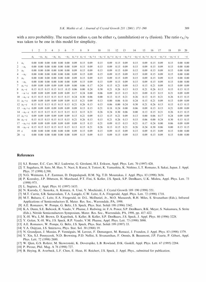
with a zero probability. The reaction radius rI can be either rA (annihilation) or rF (fusion). The ratio rA=rFwas taken to be one in this model for simplicity.
1 2 3 4 5 6 7 8 9 10 11 12 13 14 15 16 17 18 19 20
a1 �a1 a2 �a2 a3 �a3 a1+c a1�c �a1+c �a1�c a2+c a2�c �a2+c �a2�c a3+c a3�c �a3+c �a3�c c �c
1 a1 0.00 0.00 0.00 0.00 0.00 0.00 0.09 0.15 0.09 0.15 0.09 0.15 0.09 0.15 0.09 0.15 0.09 0.15 0.00 0.00
2 �a1 0.00 0.00 0.00 0.00 0.00 0.00 0.09 0.15 0.09 0.15 0.09 0.15 0.09 0.15 0.09 0.15 0.09 0.15 0.00 0.00
3 a2 0.00 0.00 0.00 0.00 0.00 0.00 0.09 0.15 0.09 0.15 0.09 0.15 0.09 0.15 0.09 0.15 0.09 0.15 0.00 0.00
4 �a2 0.00 0.00 0.00 0.00 0.00 0.00 0.09 0.15 0.09 0.15 0.09 0.15 0.09 0.15 0.09 0.15 0.09 0.15 0.00 0.00
5 a3 0.00 0.00 0.00 0.00 0.00 0.00 0.09 0.15 0.09 0.15 0.09 0.15 0.09 0.15 0.09 0.15 0.09 0.15 0.00 0.00
6 �a3 0.00 0.00 0.00 0.00 0.00 0.00 0.09 0.15 0.09 0.15 0.09 0.15 0.09 0.15 0.09 0.15 0.09 0.15 0.00 0.00
7 a1+c 0.09 0.09 0.09 0.09 0.09 0.09 0.00 0.06 0.17 0.24 0.15 0.21 0.09 0.13 0.15 0.21 0.09 0.13 0.09 0.09
8 a1�c 0.15 0.15 0.15 0.15 0.15 .0.15 0.06 0.00 0.24 0.30 0.21 0.26 0.13 0.15 0.21 0.26 0.13 0.15 0.15 0.15
9 �a+c 0.09 0.09 0.09 0.09 0.09 0.09 0.17 0.24 0.00 0.06 0.09 0.13 0.15 0.21 0.09 0.13 0.15 0.21 0.09 0.09
10 �a1�c 0.15 0.15 0.15 0.15 0.15 0.15 0.24 0.30 0.06 0.00 0.13 0.15 0.21 0.26 0.13 0.15 0.21 0.26 0.15 0.15
11 a2+c 0.09 0.09 0.09 0.09 0.09 0.09 0.15 0.21 0.09 0.13 0.00 0.06 0.18 0.24 0.15 0.21 0.09 0.13 0.09 0.09
12 a2�c 0.15 0.15 0.15 0.15 0.15 0.15 0.21 0.26 0.13 0.15 0.06 0.00 0.24 0.30 0.21 0.26 0.13 0.15 0.15 0.15
13 �a2+c 0.09 0.09 0.09 0.09 0.09 0.09 0.09 0.13 0.15 0.21 0.18 0.24 0.00 0.06 0.09 0.13 0.15 0.21 0.09 0.09
14 �a2�c 0.15 0.15 0.15 0.15 0.15 0.15 0.13 0.15 0.21 0.26 0.24 0.30 0.06 0.00 0.13 0.15 0.21 0.26 0.15 0.15
15 a3+c 0.09 0.09 0.09 0.09 0.09 0.09 0.15 0.21 0.09 0.13 0.15 0.21 0.09 0.13 0.00 0.06 0.17 0.24 0.09 0.09
16 a3�c 0.15 0.15 0.15 0.15 0.15 0.15 0.21 0.26 0.13 0.15 0.21 0.26 0.13 0.15 0.06 0.00 0.24 0.30 0.15 0.15
17 �a3+c 0.09 0.09 0.09 0.09 0.09 0.09 0.09 0.13 0.15 0.21 0.09 0.13 0.15 0.21 0.17 0.24 0.00 0.06 0.09 0.09
18 �a3�c 0.15 0.15 0.15 0.15 0.15 0.15 0.13 0.15 0.21 0.26 0.13 0.15 0.21 0.26 0.24 0.30 0.06 0.00 0.15 0.15
19 c 0.00 0.00 0.00 0.00 0.00 0.00 0.09 0.15 0.09 0.15 0.09 0.15 0.09 0.15 0.09 0.15 0.09 0.15 0.00 0.00
20 �c 0.00 0.00 0.00 0.00 0.00 0.00 0.09 0.15 0.09 0.15 0.09 0.15 0.09 0.15 0.09 0.15 0.09 0.15 0.00 0.00
References
[1] S.J. Rosner, E.C. Carr, M.J. Ludowise, G. Girolami, H.I. Erikson, Appl. Phys. Lett. 70 (1997) 420.
[2] T. Sugahara, H. Sato, M. Hao, Y. Naoi, S. Kurai, S. Tottori, K. Yamashita, K. Nishino, L.T. Romano, S. Sakai, Japan. J. Appl.
Phys. 37 (1998) L398.
[3] N.G. Weimann, L.F. Eastman, D. Doppalapudi, H.M. Ng, T.D. Moustakas, J. Appl. Phys. 83 (1998) 3656.
[4] P. Kozodoy, J.P. Ibbetson, H. Marchand, P.T. Fini, S. Keller, J.S. Speck, S.P. DenBaars, U.K. Mishra, Appl. Phys. Lett. 73
(1998) 975.
[5] L. Sugiura, J. Appl. Phys. 81 (1997) 1633.
[6] N. Kuroda, C. Sasaoka, A. Kimura, A. Usui, Y. Mochizuki, J. Crystal Growth 189–190 (1998) 551.
[7] M.T. Currie, S.B. Samavedam, T.A. Langdo, C.W. Leitz, E.A. Fitzgerald, Appl. Phys. Lett. 72 (1998) 1718.
[8] M.T. Bulsara, C. Leitz, E.A. Fitzgerald, in: D.L. McDaniel, Jr., M.O. Manasreh, R.H. Miles, S. Sivanathan (Eds.), Infrared
Applications of Semiconductors II, Mater. Res. Soc., Warrendale, PA, 1998.
[9] A.E. Romanov, W. Pompe, G. Beltz, J.S. Speck, Phys. Stat. Solidi 198 (1996) 3342.
[10] K.A. Dunn, S.E. Babcock, R. Vaudo, V. Phanse, J. Redwing, in: F.A. Ponce, S.P. DenBaars, B.K. Meyer, S. Nakamura, S. Strite
(Eds.), Nitride Semiconductors Symposium, Mater. Res. Soc., Warrendale, PA, 1998, pp. 417–422.
[11] X.-H. Wu, L.M. Brown, D. Kapolnek, S. Keller, B. Keller, S.P. DenBaars, J.S. Speck, J. Appl. Phys. 80 (1996) 3228.
[12] Y. Golan, X.-H. Wu, J.S. Speck, R.P. Vaudo, V.M. Phanse, Appl. Phys. Lett. 73 (1998) 3090.
[13] A.E. Romanov, W. Pompe, G. Beltz, J.S. Speck, Phys. Stat. Solidi 199 (1997) 33.
[14] Y.A. Osipyan, I.S. Smirnova, Phys. Stat. Sol. 30 (1968) 19.
[15] N. Grandjean, J. Massies, P. Venn!egu"es, M. Leroux, F. Demangeot, M. Renucci, J. Frandon, J. Appl. Phys. 83 (1998) 1379.
[16] Y. Xin, S.J. Pennycook, N.D. Browning, P.D. Nellist, S. Sivananthan, F. Omn"es, B. Beaumont, J.P. Faurie, P. Gibart, Appl.
Phys. Lett. 72 (1998) 2680.
[17] W. Qian, G.S. Rohrer, M. Skowronski, K. Doverspike, L.B. Rowland, D.K. Gaskill, Appl. Phys. Lett. 67 (1995) 2284.
[18] P. Pirouz, Phil. Mag. A 78 (1998) 727.
[19] B. Heying, R. Averbeck, L.F. Chen, E. Haus, H. Reichert, J.S. Speck, J. Appl. Phys., submitted for publication.
S.K. Mathis et al. / Journal of Crystal Growth 231 (2001) 371–390 389
[20] E.A. Fitzgerald, J. Vac. Sci. Technol. B 7 (1989) 782.
[21] J.S. Speck, M.A. Brewer, G. Beltz, A.E. Romanov, W. Pompe, J. Appl. Phys. 80 (1996) 3808.
[22] M. Chang, G. Beltz, S. Mathis, Fall 1998 MRS Proceedings, III–V and IV–V Materials and Processing Challenges for Highly
Integrated Microelectronics and Optoelectronics, to be published.
[23] S.K. Mathis, X.H. Wu, A.E. Romanov, J.S. Speck, J. Appl. Phys. 86 (1999) 4836.
[24] L.T. Romano, B.S. Krusor, R.J. Molnar, Appl. Phys. Lett. 71 (1997) 2283.
[25] K.A. Dunn, S.E. Babcock, R. Vaudo, V. Phanse, J. Redwing, in: F.A. Ponce, S.P. DenBaars, B.K. Meyer, S. Nakamura, S. Strite
(Eds.), Nitride Semiconductors Symposium, Mater. Res. Soc., Warrendale, PA, 1998, pp. 417–422.
[26] D. Kapolnek, X.H. Wu, B. Heying, S. Keller, B.P. Keller, U.K. Mishra, S.P. DenBaars, J.S. Speck, Appl. Phys. Lett. 67 (1995)
1541.
[27] P. Gay, P.B. Hirsch, A. Kelly, Acta Met. 1 (1953) 315.
[28] J.E. Ayers, J. Crystal Growth 135 (1994) 71.
[29] S. Keller, B.P. Keller, Y.-F. Wu, B. Heying, D. Kapolnek, J.S. Speck, U.K. Mishra, S.P. DenBaars, Appl. Phys. Lett. 68 (1996)
1525.
[30] B. Heying, X.H. Wu, S. Keller, Y. Li, D. Kapolnek, B.P. Keller, S.P. DenBaars, J.S. Speck, Appl. Phys. Lett. 68 (1996) 643.
S.K. Mathis et al. / Journal of Crystal Growth 231 (2001) 371–390390