modeling and trade-off analysis of a capacitive silicon
TRANSCRIPT
Modeling and trade-off analysis of a capacitivesilicon Mach-Zehnder modulator for telecom
applications
Diego M. Dourado, Monica L. Rochaand Joao Paulo P. Carmo
Electrical and Computer EngineeringDepartment EESC, USP
Sao Carlos, [email protected]
Giovanni B. FariasDivision of Optical Technologies CPqD
Campinas, [email protected]
Joao E. RibeiroPolytechnic Institute of Braganca
Santa Apolonia campusBraganca, Portugal
Abstract—This paper presents a capacitive modulator designand modeling using poly-si and silicon technologies. We proposea methodology involving the entire modulator design process,from the optical design, charge distribution calculation andsmall-signal RF analysis. Thus, in the case of silicon photonicsmodulators, the paper proposes means to optimize the trade-offsamong several figures of merit. It is shown that high bandwidthoperation (>30 GHz) can be achieved by sacrificing a little themodulation efficiency.
Index Terms—silicon photonics, mach-zehnder, capacitivemodulator, modal analysis, optical devices
I. INTRODUCTION
Optical technologies are playing a crucial role in sustaininghigh bandwidth demand. Due to the exponential increase indata consumption by fixed and mobile broadband subscribers,growing bandwidth demand by high-definition video services,silicon photonics devices emerges as a potential solutionfor future generations of optical fiber systems, from short-reach interconnect, access and metropolitan networks [1].One of the main advantages of silicon photonics technolo-gies is its compatibility with complementary metal-oxide-semiconductor (CMOS) processes, which enables monolithicintegration with electronic circuits. In addition, the CMOStechnology has the potential for delivering reliable devices andlarge manufacturing scale, resulting in a low cost per device.
High-speed modulators based on the carrier depletion mech-anism have been investigated for years [2]. These types ofdevices have modulation efficiency in the order of 2 V.cm,which requires long modulators (>3 mm) to have low Vπ .Because of that, the modulator behaves as travelling-wavesince its length is longer than the RF wavelength. On theother hand, capacitive modulators that use carrier accumula-tion mechanism can have modulation efficiency an order of
The research received funding from CAPES and FAPESP (under grant2016/20615-8).
magnitude higher than depletion modulators [3], decreasingthe modulator length required. In this way, the modulatorbehaves as a lumped element which simplify its design [4].
Capacitive modulators can be implemented by using anlayer of poly-Si above the silicon waveguide, with a thinoxide layer as a gate. The use of poly-Si is compatible withCMOS process and present in most silicon-on-insulator (SOI)platforms [5]. High performance capacitive modulators in thisconfiguration have been reported in [3], [6], [7]. Due to theirhigh bandwidth performance and modulation efficiency, suchdevices continue to be studied to provide increasingly efficientparameters.
The main objective of this work is to propose a designmethodology to study the behaviour of the capacitive modula-tors with poly-Si configuration. Some device parameters suchas waveguide width, doping conditions and gate thickness arestudied to explore the trade-off between modulation efficiency,optical loss and modulation bandwidth.
The paper is organized in five parts. Section II addresses thedevice structure that will be modeled based on commerciallyavailable technologies. By means of modal analysis, in sec-tion III the waveguide width is discussed. Section IV targetsthe best charge distribution to assess loss and modulationefficiency. Section V performs a dynamic analysis of themodulator, from modulation efficiency to bandwidth by meansof RF analysis. Finally, section VI presents a brief conclusion.
II. DEVICE STRUCTURE
Figure 1 shows the modulator schematic, where W is thewaveguide width, tgate is the oxide gate thickness, tpoly is thepoly-Si thickness, tSi is the silicon thickness and, finally, tslabis the Si slab thickness.
It is possible to observe that the poly-Si has n-type dopingand the silicon has p-type doping. The doping level becomeshigher when the colors (blue and red) become darker. There-978-1-5386-6702-6/18/$31.00 ©2018 IEEE

Fig. 1: Cross section view of the capacitive modulator pro-posed.
fore, the modulator is designated with three concentrationlevels.
Due to the unavailability of real poly-Si parameters for anaccurate simulation, we chose to use silicon parameters in bothparts of the waveguide, the top and bottom region. The device’sdimensional parameters were defined as: tpoly = 160 nm,tSi = 220 nm, tslab = 70 nm and tgate = 15 nm, whichare in accordance with most SOI platforms. A study of thew1 and w2 widths will be discussed to optimize the trade-off between optical insertion loss and modulation bandwidth(access resistance). The ratio between these parameters wasset to w1 + w2 = 1 µm to minimize propagation loss [7].
High PBODY/NBODY doping was set according to foundryparameters. The corresponding resistivity for each dopingconcentration was calculated as:
R = Rs ×Wi (1)
where Wi is the width that corresponds a certain part of thedevice. In this case, Wi can assume the following values: W ,w1 or w2 (see Fig. 1). The sheet resistance is obtained fromexperimental results in the PDK library [5].
In the electrical charge simulation, reverse bias voltagesfrom 0 to -3 volts were applied on the metal gate, while theother metal was designated as ground, as shown in Fig. 1.
Finally, all optical and charge simulations (optical and staticdesigns) were performed using commercial LUMERICAL prod-ucts. The RF simulation part (RF design) was implemented incommercial MATLAB software.
III. OPTICAL DESIGN
To design the device, the waveguide width (W ) was sweptfrom 300 to 700 nm in steps of 10 nm. Thus, by sweeping W ,it is possible to observe the fundamental propagation mode andselect a W value which provides a single propagation modethrough the waveguide with high optical confinement. Figure 2shows this analysis.
Figure 2a shows that, during the W sweep, three modes arefound in the structure. The fundamental propagation TE modeis highlighted in blue. Since we want to avoid higher ordermodes, we choose W = 500 nm so that only the fundamentalmode propagates. Values above 500 nm can provide otherunwanted modes. On the other hand, values below 500 nm can
(a)
(b)
Fig. 2: (a) Effective index (neff ) when the waveguidewidth (W ) is swept from 300 to 700 nm. (b) Optical profilewhen W is equal to 500 nm.
result in low optical confinement and hence lower modulationefficiency. Figure 2b shows the E-field intensity profile inthe waveguide. Therefore, from this point, W will be set to500 nm.
IV. STATIC MODELING
After the optical design, the next step is to calculate mod-ulation efficiency and optical loss as function of the appliedvoltage.
First, the charge distribution was calculated for severalapplied voltages using a numerical software. Doping profileswere considered homogeneous in the waveguide. Then, thecharge distribution was transferred to the modal solver. Therefractive index and absorption variation as function of thecharge concentration is calculated using Soref’s equations for1.55 µm wavelength [8].
∆n(x,y)=−[8.8×10⁻²²Ne(x,y)+8.5×10⁻¹⁸N0.8h (x,y)] (2)
∆α(x,y)=8.5×10⁻¹⁸Ne(x,y)+6×10⁻¹⁸Nh(x,y) (3)
where Ne is the electron and Nh is the hole concentration.The effective index is found using the overlap integral [4]:
neff =
∫∫∞ n(x, y)|E(x, y)|2ds∫∫∞ |E(x, y)|2ds
(4)
where n(x, y) = nSi + ∆n(x, y) and E(x, y) is the funda-mental mode electric field distribution. The optical insertionloss is found in the same way.
When addressing silicon modulators, the modulation effi-ciency (Vπ×L) is the most discussed figure of merit to evaluatethe device performance. In the case of silicon photonicsmodulators, when subjected to a voltage, the product Vπ × Lvaries non-linearly due to nonlinear variation of the siliconrefractive index. In this way, the product can be calculatedas [9]:
Vπ × L =λ
2
dV
dneff
∣∣∣V=Vbias
(5)
where λ is the wavelength and dneff is the refractive indexvariation caused by the voltage variation (dV ) applied on themetal gate.
A. Doping concentration analysis
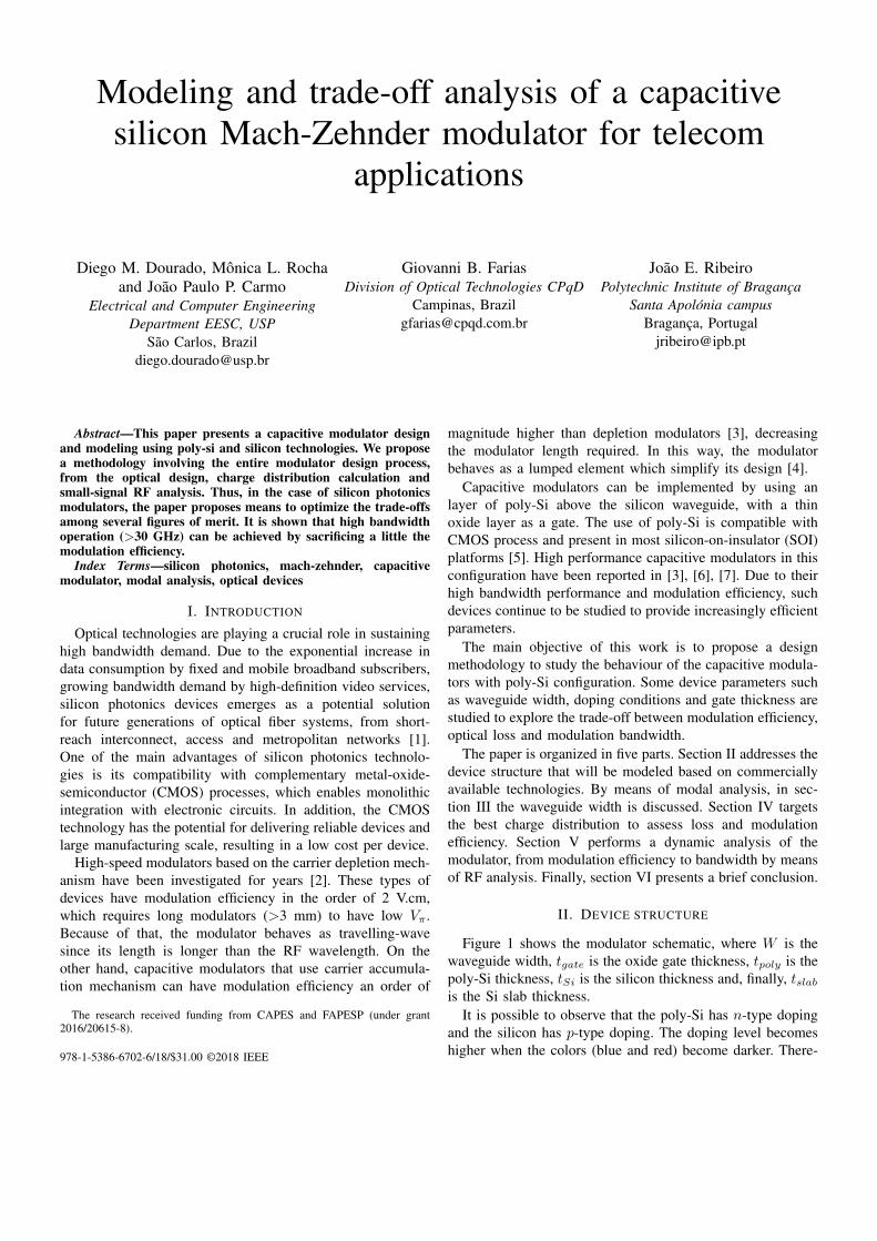
In this analysis the modulation efficiency and loss wereobserved as function of the doping concentration. For thefundamental mode, Fig. 3 outlines the optical loss level and themodulation efficiency in relation to the carrier concentrationin the waveguide, for three typical reverse bias voltage. Thelegend indicates the different Vbias for both Vπ × L and itscorresponding optical loss.
Fig. 3: Optical loss and modulation efficiency as function ofthe carrier concentration in the waveguide, for three Vbiaspoints.
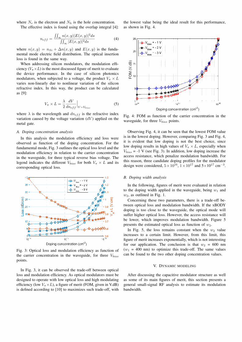
In Fig. 3, it can be observed the trade-off between opticalloss and modulation efficiency. As optical modulators must bedesigned to operate with low optical loss and high modulatingefficiency (low Vπ×L), a figure of merit (FOM, given in V.dB)is defined according to [10] to maximizes such trade-off, with
the lowest value being the ideal result for this performance,as shown in Fig. 4.
Fig. 4: FOM as function of the carrier concentration in thewaveguide, for three Vbias points.
Observing Fig. 4, it can be seen that the lowest FOM valueis in the lowest doping. However, comparing Fig. 3 and Fig. 4,it is evident that low doping is not the best choice, sincelow doping results in high values of Vπ ×L, especially whenVbias = -1 V (see Fig. 3). In addition, low doping increase theaccess resistance, which penalize modulation bandwidth. Forthis reason, three candidate doping profiles for the modulatordesign were considered, 5×10¹⁶, 1×10¹⁷ and 5×1017 cm−3.
B. Doping width analysis
In the following, figures of merit were evaluated in relationto the doping width applied in the waveguide, being w1 andw2, as outlined in Fig. 1.
Concerning these two parameters, there is a trade-off be-tween optical loss and modulation bandwidth. If the xBODYdoping is too close to the waveguide, the optical mode willsuffer higher optical loss. However, the access resistance willbe lower, which improves modulation bandwidth. Figure 5presents the estimated optical loss as function of w2.
In Fig. 5, the loss remains constant when the w2 valueincreases to a certain limit. However, from this limit, thisfigure of merit increases exponentially, which is not interestingfor our application. The conclusion is that w2 = 600 nm(w1 = 400 nm) to optimize this trade-off. The same valuescan be found to the two other doping concentration values.
V. DYNAMIC MODELING
After discussing the capacitive modulator structure as wellas some of its main figures of merit, this section presents ageneral small-signal RF analysis to estimate its modulationbandwidth.

Fig. 5: Optical loss as function of w2 for three bias voltagepoints.
A. Capacitance analysis
The oxide gate capacitance is obtained directly from thenumerical charge solver. As an example, Fig. 6 presents thecapacitance per unit length for several bias voltages.
Fig. 6: Capacitance per unit length as function of Vbias.
In Fig. 6, when increasing the reverse bias from 0 to3 Volts, the capacitance per unit length varies between 0.81and 1.30 fF/µm. As modulators are designed to operate atthe highest modulation speed, low capacitances are required.TABLE I summarizes the three figures of merit optimized forthe three dopant concentrations analyzed.
B. Electro-optical bandwidth analysis
The EO bandwidth is calculated from the method describedin [4] using the RF transmission coefficient (accountingthe impedance mismatch) and the system transfer function.Figure 7 shows the RLC equivalent circuit model for theconfiguration proposed in this paper, where Req =
∑4i=1Ri is
TABLE I: Optimized parameters in different P1/N1 doping.
P1 & N1 Vπ × L Loss C[cm−3] [V.cm] [dB/cm] [fF/µm]
5× 10160.97 @ -1 V0.74 @ -2 V0.58 @ -3 V
1.87 @ -1 V4.38 @ -2 V9.29 @ -3 V
0.96 @ -1 V1.23 @ -2 V1.28 @ -3 V
1× 10170.88 @ -1 V0.72 @ -2 V0.58 @ -3 V
3.33 @ -1 V5.82 @ -2 V
10.56 @ -3 V
1.0 @ -1 V1.24 @ -2 V1.29 @ -3 V
5× 10170.80 @ -1 V0.71 @ -2 V0.58 @ -3 V
15.21 @ -1 V17.74 @ -2 V22.58 @ -3 V
1.13 @ -1 V1.25 @ -2 V1.30 @ -3 V
the equivalent resistance resulting from the doping in differentparts of the modulator.
Fig. 7: Equivalent circuit model.
In Fig. 7, L1 is the transmission line inductance, C0 isthe pad parasitic capacitance and C1 is the capacitance onthe oxide gate. In addition, it is possible to observe theconfiguration parameters of the transmission line, where Wmt
is the metal width and Wgap is the gap between the twometal lines. Due to line and input impedance, the RF voltagetransmission can be written as:
Γ(jω) =2Zl
Zl + Z0(6)
where Zl represents the equivalent load (ReqL1C1||C0), Z0
is the input characteristic impedance and ω is the angularfrequency of the electric signal.
In addition, in (7), it is possible to observe the systemtransfer function H(jω), ratio between the voltage on oxidegate and the input voltage (Vs).
H(jω) =
1jωC1
1jωC1
+ jωL1 +Req(7)
Finally, the electro-optical response can be written as:
S21[dB]= 20 log10 |Γ(jω)H(jω)| (8)

Considering the device manufacture in the near future,the equivalent resistance as well as the waveguide dopingconcentration were calculated according to the parametersprovided by IMEC’s multi-project wafer (MPW) [5]. In thisway, Req is ∼7.1 Ω.mm and P1/N1 is ∼5× 1017 cm−3. Theinductance (L1) as a function of the operation frequency inthe transmission line were calculated according to the coplanarwaveguide (CPW) model proposed by Heinrich [11]. Finally,in order to provide higher bandwidth, the input characteristicimpedance was set to 5 Ω, as proposed in [12].
TABLE II summarizes the figures of merit including EObandwidth for two length cases for several tgate thicknesses.For each line, Wmt and Wgap are optimized to provide thehighest bandwidth.
TABLE II: Optimized parameters in different design scenariosfor Vbias = -1 V.
tgate Vπ × L LossEO BW
(L = 0.5 mm)EO BW
(L = 1 mm)[nm] [V.cm] [dB/cm] [GHz] [GHz]
5 0.45 16.57 9.58 7.3615 0.80 15.21 19.35 12.4525 1.25 14.81 25.23 15.2035 1.64 14.66 29.35 17.1945 2.32 14.58 32.54 18.76
In TABLE II, it is possible to note that the electro-opticalbandwidth increases with the gate thickness. However, thedevice configuration will be the designer’s choice, since themodulation efficiency behaves inversely to EO bandwidth.Figure 8 outlines the electro-optical response for three tgatepoints. For the analysis of these three curves, the transmissionline parameters Wmt and Wgap were set to ∼64 µm and∼24 µm, respectively.
Fig. 8: Electro-optical response for Vbias = -1 V.
VI. CONCLUSION
In this paper we present a methodology to design andoptimize silicon photonics modulators based on capacitive
junction. Trade-offs between modulation efficiency, opticalloss, modulation speed and EO bandwidth are analyzed withrespect to a few modulator physical and geometrical parame-ters. For this, three concentration profiles (5×10¹⁶, 1×10¹⁷
and 5×1017 cm−3) were analyzed to better explore thesetrade-offs. The distance from the medium-doped regions tothe waveguide was swept to optimize trade-off between accessresistance (to improve modulation speed) and optical loss. Thefinal part of the paper shows that the oxide gate thickness iscrucial for improving the electro-optical bandwidth. Thus, thegreater the oxide gate thickness, the lower the capacitanceon the SiO2 gate and, as a result, the greater the bandwidthoffered. On the other hand, this scenario decreases the mod-ulation efficiency and may require high voltages to drive thedevice. In spite of the fact that the design results have notachieved a high modulation efficiency with high modulationspeed, the methodology presented here can be implementedin several silicon photonics modulators, and can be usedto explore alternatives to improve these results. In addition,to improve the model accuracy, the poly-Si experimentalparameters must be obtained.
REFERENCES
[1] D. M. Dourado, R. J. L. Ferreira, M. de Lacerda Rocha, and U. R.Duarte, “Energy consumption and bandwidth allocation in passiveoptical networks,” Optical Switching and Networking, vol. 28, pp. 1–7, 2018.
[2] D. A. Motta, Y. R. R. Bustamante, A. P. Freitas, G. B. de Farias,U. C. Moura, and L. H. Gabrielli, “Design of a 40 ghz bandwidthslow-wave silicon modulator,” in 2017 SBMO/IEEE MTT-S InternationalMicrowave and Optoelectronics Conference (IMOC), Aug 2017, pp. 1–5.
[3] B. Milivojevic, C. Raabe, A. Shastri, M. Webster, P. Metz, S. Sunder,B. Chattin, S. Wiese, B. Dama, and K. Shastri, “112gb/s dp-qpsktransmission over 2427km ssmf using small-size silicon photonic iqmodulator and low-power cmos driver,” in 2013 Optical Fiber Com-munication Conference and Exposition and the National Fiber OpticEngineers Conference (OFC/NFOEC), March 2013, pp. 1–3.
[4] X. Li, F. Yang, F. Zhong, Q. Deng, J. Michel, and Z. Zhou, “Single-drivehigh-speed lumped depletion-type modulators toward 10 fj/bit energyconsumption,” Photon. Res., vol. 5, no. 2, pp. 134–142, Apr 2017.
[5] IMEC, imec-ePIXfab SiPhotonics: iSiPP50G, IMEC.[6] M. Webster, C. Appel, P. Gothoskar, S. Sunder, B. Dama, and K. Shastri,
“Silicon photonic modulator based on a mos-capacitor and a cmosdriver,” in 2014 IEEE Compound Semiconductor Integrated CircuitSymposium (CSICS), Oct 2014, pp. 1–4.
[7] S. Zhu and G. Q. Lo, “Designs of silicon mis phase modulator with adeposited aln film as the gate dielectric,” IEEE Photonics TechnologyLetters, vol. 27, no. 11, pp. 1236–1239, June 2015.
[8] G. T. Reed and A. P. Knights, Silicon Photonics, an Introduction. JohnWiley & Sons Ltd, 2004.
[9] Y. Zhou, L. Zhou, H. Zhu, C. Wong, Y. Wen, L. Liu, X. Li, and J. Chen,“Modeling and optimization of a single-drive push-pull silicon mach-zehnder modulator,” Photon. Res., vol. 4, no. 4, pp. 153–161, Aug 2016.
[10] I. Goykhman, B. Desiatov, S. Ben-Ezra, J. Shappir, and U. Levy,“Optimization of efficiency-loss figure of merit in carrier-depletionsilicon mach-zehnder optical modulator,” Opt. Express, vol. 21, no. 17,pp. 19 518–19 529, Aug 2013.
[11] W. Heinrich, “Quasi-tem description of mmic coplanar lines includingconductor-loss effects,” IEEE Transactions on Microwave Theory andTechniques, vol. 41, no. 1, pp. 45–52, Jan 1993.
[12] S. Zhou, H. ta Wu, K. Sadeghipour, C. Scarcella, C. Eason, M. Rensing,M. J. Power, C. Antony, P. O’Brien, P. D. Townsend, and P. Ossieur,“Optimization of pam-4 transmitters based on lumped silicon photonicmzms for high-speed short-reach optical links,” Opt. Express, vol. 25,no. 4, pp. 4312–4325, Feb 2017.