modeling of avalanche breakdown in silicon and gallium
TRANSCRIPT

Photos placed in horizontal position
with even amount of white space
between photos and header
This presentation describes objective technical results and analysis. Any subjective views or opinions that might be
expressed in the paper do not necessarily represent the views of the U.S. Department of Energy or the United
States Government. Sandia National Laboratories is a multimission laboratory managed and operated by National
Technology & Engineering Solutions of Sandia, LLC, a wholly owned subsidiary of Honeywell International Inc., for
the U.S. Department of Energy’s National Nuclear Security Administration under contract DE-NA0003525
Modeling of Avalanche Breakdown in Silicon and Gallium Nitride High-Voltage Diodes using COMSOL®
J. Dickerson, R. J. Kaplar, and G. Pickrell

Power Diodes
VB
An ideal diode is the perfect switch.
Reverse blocking limited by the breakdown voltage VB.
Jeramy Dickerson
𝑉 ≤ 0I = 0
R = ∞
Normal device I-V curve.
R = 0
2

Impact Ionization and Avalanche Breakdown
Energetic electron
1. A carrier gains energy as it is propelled by the local electric field.
2. At a sufficiently high energy, greater than Eg, collision with an atomtransfers extra energy to the atom, and ionizes an electron-hole pair.
Avalanche breakdown: When the impact ionization process causes the current to increase by orders of magnitude with only a small increase in the applied voltage.
Ec
Ev
The Impact Ionization (II) Process :
3
Jeramy Dickerson

A good starting point is to calculate the planar junction breakdownvoltage. This gives the upper limit on the device performance.
p+
n+
n-
The Planar Junction Diode
6
Jeramy Dickerson

A planar junction devices has a uniform electric field. The wavy line shown is anartifact of the free triangular mesh used. For a 1e14 cm-3 doped 20 um thickdrift region the simulation fails to converge at -448.5 V which is the devicebreakdown voltage.
Silicon Planar Device
7
Jeramy Dickerson
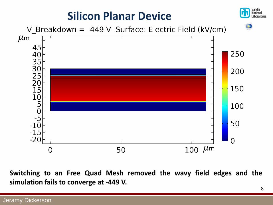
Switching to an Free Quad Mesh removed the wavy field edges and thesimulation fails to converge at -449 V.
Silicon Planar Device
8
Jeramy Dickerson

Edge Termination
Official Use Only9
n+ region
n- region
p+ region
Anode
Edge Termination, in this case an insulating layer.
Physically realizable devicescannot have infinite parallelplanes.
The electric field crowding effect is seen onsharp corners of doping profiles. This leadsto premature breakdown in devices.
Jeramy Dickerson

10
Lots of ideas have been suggested to manage field crowding effects:
• Guard rings
• Field plates
• Beveled surfaces
• Etch contours
• Junction termination extensions
Edge Termination Schemes
B. Jayant Baliga, “High-voltage device termination techniques a comparative review” IEE Proceedings I (Solid-State and Electron Devices), Volume 129, Issue 5, October 1982, p. 173 – 179
Jeramy Dickerson
11
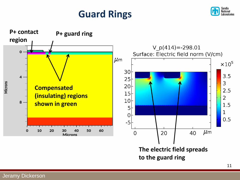
Guard Rings
P+ contact region
P+ guard ring
Compensated (insulating) regions shown in green
The electric field spreads to the guard ring
Jeramy Dickerson
12
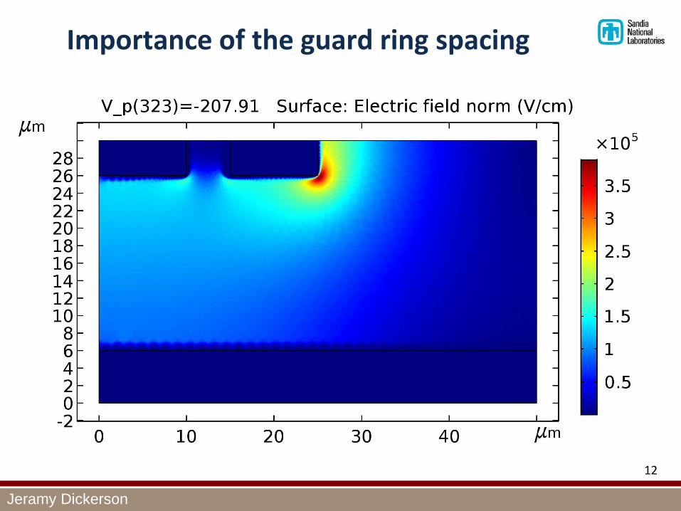
Importance of the guard ring spacing
Jeramy Dickerson

13
Importance of the guard ring spacing
Jeramy Dickerson
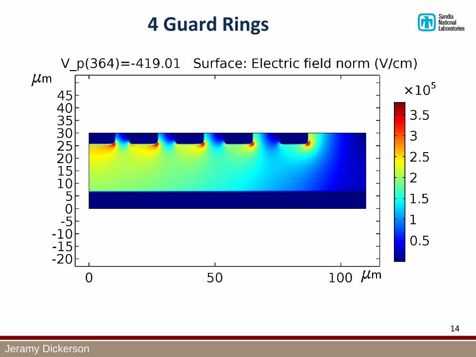
4 Guard Rings
14
Jeramy Dickerson

Converting to GaN
Need to add carrier lifetimes and mobilities
Need to refine the stepsize of the voltage sweep. While 1 V steps worked for the Silicon devices, 0.05 V led to good convergence in GaN.
Changed the drift region doping from 1e14 cm-3 in Si to 2e16 cm-3 in GaN. Lower is better for breakdown, however obtaining low doping in GaN is challenging.
Need to change the impact ionization model parameters.
17
Jeramy Dickerson

Converting to GaN
Most importantly you need to change the impact ionization model.
18
Okuto Crowell Model (from COMSOL interface)
Jeramy Dickerson

Converting to GaN
19
Si: an = 0.426; ap = 0.243; bn = 4.81e5; bp=6.53e5; etc (default)Si critical electic field ~350 kV/cm
GaN: an=ap=4.3; bn=bp=1.05e7; cn=cp=dn=dp=0 (ignore temperature dependence)GaN critical electric field ~4.0 MV/cmThese GaN numbers are calculated to achieve a 4 MV/cm critical electric field. They are not from literature, empirical data, and have not been validated!
Jeramy Dickerson

A cutline of the electric field profile shows we are indeed approaching 4 MV/cm atbreakdown. The profile also indicates the depletion depth is only 10 um. The highdoping of 2e16 means that a 20 um drift region is twice as thick as we need.
GaN Planar Electric Field at Breakdown
8
Jeramy Dickerson

The breakdown of this device is over 2100 V!
GaN Reverse Bias Current-Voltage
8
Jeramy Dickerson
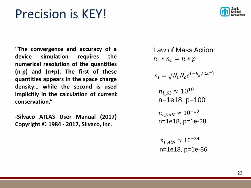
Precision is KEY!
22
“The convergence and accuracy of adevice simulation requires thenumerical resolution of the quantities(n-p) and (n+p). The first of thesequantities appears in the space chargedensity… while the second is usedimplicitly in the calculation of currentconservation.”
-Silvaco ATLAS User Manual (2017)Copyright © 1984 - 2017, Silvaco, Inc.
Law of Mass Action:
𝑛𝑖 ∗ 𝑛𝑖 = 𝑛 ∗ 𝑝
𝑛𝑖 = 𝑁𝑣𝑁𝑐𝑒 −𝐸𝑔 2𝑘𝑇
𝑛𝑖_𝑆𝑖 ≈ 1010
n=1e18, p=100
𝑛𝑖_𝐺𝑎𝑁 ≈ 10−10
𝑛𝑖_𝐴𝑙𝑁 ≈ 10−34
n=1e18, p=1e-28
n=1e18, p=1e-86

Precision is KEY!
23
Silvaco ATLAS User Manual(2017) Copyright © 1984 -2017, Silvaco, Inc.
COMSOL simulations seem to accurately calculate breakdown in simple 2D structures for Silicon and for the planar configuration for GaN.
GaN parameters for breakdown are not known for the Okuto Crowell model. Adding other models, such as the simple Shockley model, would allow for empirically calculated values to be used.
Wide bandgap materials, which are gaining lots of attention in the semiconductor community need more precision. This is a plug for COMSOL to add some more .
n+p=1000000000000000000.0000000000000000000000000001
24
Conclusion
Jeramy Dickerson