miniature penning cell array for on-chip...
TRANSCRIPT
MINIATURE PENNING CELL ARRAY FOR ON-CHIP VACUUM PUMPING Scott R. Green and Yogesh B. Gianchandani
University of Michigan Engineering Research Center for Wireless Integrated Microsystems (WIMS), Ann Arbor, Michigan, USA
ABSTRACT This paper presents a miniaturized Penning cell array
for on-chip sputter-ion vacuum pumping. The effects of miniaturization on pumping performance – including cut-off magnetic flux, pumping rate, and minimum operating pressure – are examined. The pump is experimentally shown to reduce pressure by 600 mTorr (80 Pa) from a starting pressure of 18 Torr (2.4 kPa) in 30 minutes of operation. The rate of molecular removal is typically 3-15 x 1013 molecules per second. The architecture allows device operation at pressures at least as low as 70 mTorr (9.3 Pa), representing an improvement of two orders of magnitude over previously reported micro-sputter-ion pumps.
INTRODUCTION On-chip vacuum generation is an attractive alternative
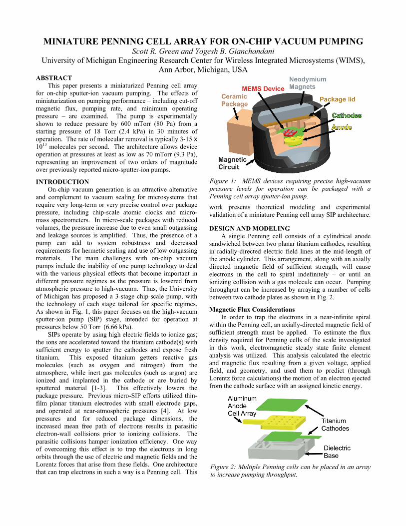
and complement to vacuum sealing for microsystems that require very long-term or very precise control over package pressure, including chip-scale atomic clocks and micro-mass spectrometers. In micro-scale packages with reduced volumes, the pressure increase due to even small outgassing and leakage sources is amplified. Thus, the presence of a pump can add to system robustness and decreased requirements for hermetic sealing and use of low outgassing materials. The main challenges with on-chip vacuum pumps include the inability of one pump technology to deal with the various physical effects that become important in different pressure regimes as the pressure is lowered from atmospheric pressure to high-vacuum. Thus, the University of Michigan has proposed a 3-stage chip-scale pump, with the technology of each stage tailored for specific regimes. As shown in Fig. 1, this paper focuses on the high-vacuum sputter-ion pump (SIP) stage, intended for operation at pressures below 50 Torr (6.66 kPa).
SIPs operate by using high electric fields to ionize gas; the ions are accelerated toward the titanium cathode(s) with sufficient energy to sputter the cathodes and expose fresh titanium. This exposed titanium getters reactive gas molecules (such as oxygen and nitrogen) from the atmosphere, while inert gas molecules (such as argon) are ionized and implanted in the cathode or are buried by sputtered material [1-3]. This effectively lowers the package pressure. Previous micro-SIP efforts utilized thin-film planar titanium electrodes with small electrode gaps, and operated at near-atmospheric pressures [4]. At low pressures and for reduced package dimensions, the increased mean free path of electrons results in parasitic electron-wall collisions prior to ionizing collisions. The parasitic collisions hamper ionization efficiency. One way of overcoming this effect is to trap the electrons in long orbits through the use of electric and magnetic fields and the Lorentz forces that arise from these fields. One architecture that can trap electrons in such a way is a Penning cell. This
work presents theoretical modeling and experimental validation of a miniature Penning cell array SIP architecture.
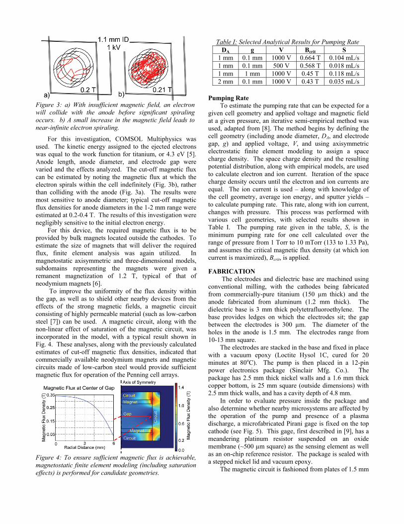
DESIGN AND MODELING A single Penning cell consists of a cylindrical anode
sandwiched between two planar titanium cathodes, resulting in radially-directed electric field lines at the mid-length of the anode cylinder. This arrangement, along with an axially directed magnetic field of sufficient strength, will cause electrons in the cell to spiral indefinitely – or until an ionizing collision with a gas molecule can occur. Pumping throughput can be increased by arraying a number of cells between two cathode plates as shown in Fig. 2.
Magnetic Flux Considerations In order to trap the electrons in a near-infinite spiral
within the Penning cell, an axially-directed magnetic field of sufficient strength must be applied. To estimate the flux density required for Penning cells of the scale investigated in this work, electromagnetic steady state finite element analysis was utilized. This analysis calculated the electric and magnetic flux resulting from a given voltage, applied field, and geometry, and used them to predict (through Lorentz force calculations) the motion of an electron ejected from the cathode surface with an assigned kinetic energy.
Figure 1: MEMS devices requiring precise high-vacuum pressure levels for operation can be packaged with a Penning cell array sputter-ion pump.
Figure 2: Multiple Penning cells can be placed in an array to increase pumping throughput.
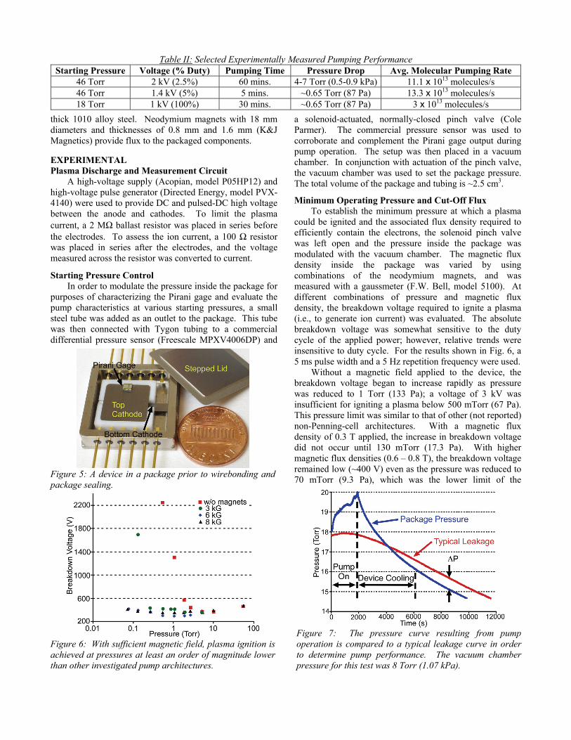
For this investigation, COMSOL Multiphysics was used. The kinetic energy assigned to the ejected electrons was equal to the work function for titanium, or 4.3 eV [5]. Anode length, anode diameter, and electrode gap were varied and the effects analyzed. The cut-off magnetic flux can be estimated by noting the magnetic flux at which the electron spirals within the cell indefinitely (Fig. 3b), rather than colliding with the anode (Fig. 3a). The results were most sensitive to anode diameter; typical cut-off magnetic flux densities for anode diameters in the 1-2 mm range were estimated at 0.2-0.4 T. The results of this investigation were negligibly sensitive to the initial electron energy.
For this device, the required magnetic flux is to be provided by bulk magnets located outside the cathodes. To estimate the size of magnets that will deliver the required flux, finite element analysis was again utilized. In magnetostatic axisymmetric and three-dimensional models, subdomains representing the magnets were given a remanent magnetization of 1.2 T, typical of that of neodymium magnets [6].
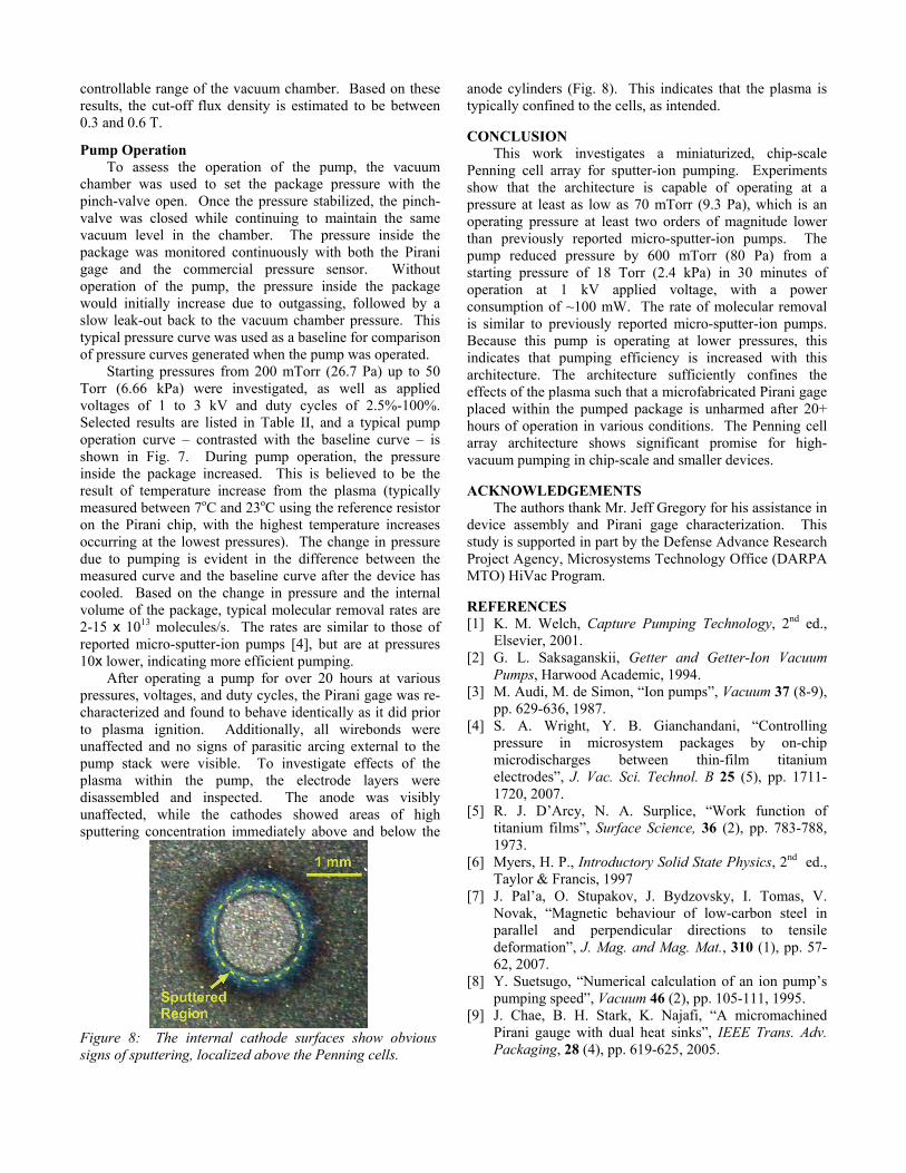
To improve the uniformity of the flux density within the gap, as well as to shield other nearby devices from the effects of the strong magnetic fields, a magnetic circuit consisting of highly permeable material (such as low-carbon steel [7]) can be used. A magnetic circuit, along with the non-linear effect of saturation of the magnetic circuit, was incorporated in the model, with a typical result shown in Fig. 4. These analyses, along with the previously calculated estimates of cut-off magnetic flux densities, indicated that commercially available neodymium magnets and magnetic circuits made of low-carbon steel would provide sufficient magnetic flux for operation of the Penning cell arrays.
Pumping Rate To estimate the pumping rate that can be expected for a
given cell geometry and applied voltage and magnetic field at a given pressure, an iterative semi-empirical method was used, adapted from [8]. The method begins by defining the cell geometry (including anode diameter, DA, and electrode gap, g) and applied voltage, V, and using axisymmetric electrostatic finite element modeling to assign a space charge density. The space charge density and the resulting potential distribution, along with empirical models, are used to calculate electron and ion current. Iteration of the space charge density occurs until the electron and ion currents are equal. The ion current is used – along with knowledge of the cell geometry, average ion energy, and sputter yields – to calculate pumping rate. This rate, along with ion current, changes with pressure. This process was performed with various cell geometries, with selected results shown in Table I. The pumping rate given in the table, S, is the minimum pumping rate for one cell calculated over the range of pressure from 1 Torr to 10 mTorr (133 to 1.33 Pa), and assumes the critical magnetic flux density (at which ion current is maximized), Bcrit, is applied.
FABRICATION The electrodes and dielectric base are machined using
conventional milling, with the cathodes being fabricated from commercially-pure titanium (150 µm thick) and the anode fabricated from aluminum (1.2 mm thick). The dielectric base is 3 mm thick polytetrafluoroethylene. The base provides ledges on which the electrodes sit; the gap between the electrodes is 300 µm. The diameter of the holes in the anode is 1.5 mm. The electrodes range from 10-13 mm square.
The electrodes are stacked in the base and fixed in place with a vacuum epoxy (Loctite Hysol 1C, cured for 20 minutes at 80oC). The pump is then placed in a 12-pin power electronics package (Sinclair Mfg. Co.). The package has 2.5 mm thick nickel walls and a 1.6 mm thick copper bottom, is 25 mm square (outside dimensions) with 2.5 mm thick walls, and has a cavity depth of 4.8 mm.
In order to evaluate pressure inside the package and also determine whether nearby microsystems are affected by the operation of the pump and presence of a plasma discharge, a microfabricated Pirani gage is fixed on the top cathode (see Fig. 5). This gage, first described in [9], has a meandering platinum resistor suspended on an oxide membrane (~500 µm square) as the sensing element as well as an on-chip reference resistor. The package is sealed with a stepped nickel lid and vacuum epoxy.
The magnetic circuit is fashioned from plates of 1.5 mm
Figure 3: a) With insufficient magnetic field, an electron will collide with the anode before significant spiraling occurs. b) A small increase in the magnetic field leads to near-infinite electron spiraling.
Figure 4: To ensure sufficient magnetic flux is achievable, magnetostatic finite element modeling (including saturation effects) is performed for candidate geometries.
Table I: Selected Analytical Results for Pumping Rate DA g V Bcrit S
1 mm 0.1 mm 1000 V 0.664 T 0.104 mL/s 1 mm 0.1 mm 500 V 0.568 T 0.018 mL/s 1 mm 1 mm 1000 V 0.45 T 0.118 mL/s 2 mm 0.1 mm 1000 V 0.43 T 0.035 mL/s
thick 1010 alloy steel. Neodymium magnets with 18 mm diameters and thicknesses of 0.8 mm and 1.6 mm (K&J Magnetics) provide flux to the packaged components.
EXPERIMENTAL Plasma Discharge and Measurement Circuit
A high-voltage supply (Acopian, model P05HP12) and high-voltage pulse generator (Directed Energy, model PVX-4140) were used to provide DC and pulsed-DC high voltage between the anode and cathodes. To limit the plasma current, a 2 MΩ ballast resistor was placed in series before the electrodes. To assess the ion current, a 100 Ω resistor was placed in series after the electrodes, and the voltage measured across the resistor was converted to current.
Starting Pressure Control In order to modulate the pressure inside the package for
purposes of characterizing the Pirani gage and evaluate the pump characteristics at various starting pressures, a small steel tube was added as an outlet to the package. This tube was then connected with Tygon tubing to a commercial differential pressure sensor (Freescale MPXV4006DP) and
a solenoid-actuated, normally-closed pinch valve (Cole Parmer). The commercial pressure sensor was used to corroborate and complement the Pirani gage output during pump operation. The setup was then placed in a vacuum chamber. In conjunction with actuation of the pinch valve, the vacuum chamber was used to set the package pressure. The total volume of the package and tubing is ~2.5 cm3.
Minimum Operating Pressure and Cut-Off Flux To establish the minimum pressure at which a plasma
could be ignited and the associated flux density required to efficiently contain the electrons, the solenoid pinch valve was left open and the pressure inside the package was modulated with the vacuum chamber. The magnetic flux density inside the package was varied by using combinations of the neodymium magnets, and was measured with a gaussmeter (F.W. Bell, model 5100). At different combinations of pressure and magnetic flux density, the breakdown voltage required to ignite a plasma (i.e., to generate ion current) was evaluated. The absolute breakdown voltage was somewhat sensitive to the duty cycle of the applied power; however, relative trends were insensitive to duty cycle. For the results shown in Fig. 6, a 5 ms pulse width and a 5 Hz repetition frequency were used.
Without a magnetic field applied to the device, the breakdown voltage began to increase rapidly as pressure was reduced to 1 Torr (133 Pa); a voltage of 3 kV was insufficient for igniting a plasma below 500 mTorr (67 Pa). This pressure limit was similar to that of other (not reported) non-Penning-cell architectures. With a magnetic flux density of 0.3 T applied, the increase in breakdown voltage did not occur until 130 mTorr (17.3 Pa). With higher magnetic flux densities (0.6 – 0.8 T), the breakdown voltage remained low (~400 V) even as the pressure was reduced to 70 mTorr (9.3 Pa), which was the lower limit of the
Figure 7: The pressure curve resulting from pump operation is compared to a typical leakage curve in order to determine pump performance. The vacuum chamber pressure for this test was 8 Torr (1.07 kPa).
Figure 5: A device in a package prior to wirebonding and package sealing.
Figure 6: With sufficient magnetic field, plasma ignition is achieved at pressures at least an order of magnitude lower than other investigated pump architectures.
Table II: Selected Experimentally Measured Pumping Performance Starting Pressure Voltage (% Duty) Pumping Time Pressure Drop Avg. Molecular Pumping Rate
46 Torr 2 kV (2.5%) 60 mins. 4-7 Torr (0.5-0.9 kPa) 11.1 x 10¹³ molecules/s 46 Torr 1.4 kV (5%) 5 mins. ~0.65 Torr (87 Pa) 13.3 x 10¹³ molecules/s 18 Torr 1 kV (100%) 30 mins. ~0.65 Torr (87 Pa) 3 x 10¹³ molecules/s
controllable range of the vacuum chamber. Based on these results, the cut-off flux density is estimated to be between 0.3 and 0.6 T.
Pump Operation To assess the operation of the pump, the vacuum
chamber was used to set the package pressure with the pinch-valve open. Once the pressure stabilized, the pinch-valve was closed while continuing to maintain the same vacuum level in the chamber. The pressure inside the package was monitored continuously with both the Pirani gage and the commercial pressure sensor. Without operation of the pump, the pressure inside the package would initially increase due to outgassing, followed by a slow leak-out back to the vacuum chamber pressure. This typical pressure curve was used as a baseline for comparison of pressure curves generated when the pump was operated.
Starting pressures from 200 mTorr (26.7 Pa) up to 50 Torr (6.66 kPa) were investigated, as well as applied voltages of 1 to 3 kV and duty cycles of 2.5%-100%. Selected results are listed in Table II, and a typical pump operation curve – contrasted with the baseline curve – is shown in Fig. 7. During pump operation, the pressure inside the package increased. This is believed to be the result of temperature increase from the plasma (typically measured between 7oC and 23oC using the reference resistor on the Pirani chip, with the highest temperature increases occurring at the lowest pressures). The change in pressure due to pumping is evident in the difference between the measured curve and the baseline curve after the device has cooled. Based on the change in pressure and the internal volume of the package, typical molecular removal rates are 2-15 x 1013 molecules/s. The rates are similar to those of reported micro-sputter-ion pumps [4], but are at pressures 10x lower, indicating more efficient pumping.
After operating a pump for over 20 hours at various pressures, voltages, and duty cycles, the Pirani gage was re-characterized and found to behave identically as it did prior to plasma ignition. Additionally, all wirebonds were unaffected and no signs of parasitic arcing external to the pump stack were visible. To investigate effects of the plasma within the pump, the electrode layers were disassembled and inspected. The anode was visibly unaffected, while the cathodes showed areas of high sputtering concentration immediately above and below the
anode cylinders (Fig. 8). This indicates that the plasma is typically confined to the cells, as intended.
CONCLUSION This work investigates a miniaturized, chip-scale
Penning cell array for sputter-ion pumping. Experiments show that the architecture is capable of operating at a pressure at least as low as 70 mTorr (9.3 Pa), which is an operating pressure at least two orders of magnitude lower than previously reported micro-sputter-ion pumps. The pump reduced pressure by 600 mTorr (80 Pa) from a starting pressure of 18 Torr (2.4 kPa) in 30 minutes of operation at 1 kV applied voltage, with a power consumption of ~100 mW. The rate of molecular removal is similar to previously reported micro-sputter-ion pumps. Because this pump is operating at lower pressures, this indicates that pumping efficiency is increased with this architecture. The architecture sufficiently confines the effects of the plasma such that a microfabricated Pirani gage placed within the pumped package is unharmed after 20+ hours of operation in various conditions. The Penning cell array architecture shows significant promise for high-vacuum pumping in chip-scale and smaller devices.
ACKNOWLEDGEMENTS The authors thank Mr. Jeff Gregory for his assistance in
device assembly and Pirani gage characterization. This study is supported in part by the Defense Advance Research Project Agency, Microsystems Technology Office (DARPA MTO) HiVac Program.
REFERENCES [1] K. M. Welch, Capture Pumping Technology, 2nd ed.,
Elsevier, 2001. [2] G. L. Saksaganskii, Getter and Getter-Ion Vacuum
Pumps, Harwood Academic, 1994. [3] M. Audi, M. de Simon, “Ion pumps”, Vacuum 37 (8-9),
pp. 629-636, 1987. [4] S. A. Wright, Y. B. Gianchandani, “Controlling
pressure in microsystem packages by on-chip microdischarges between thin-film titanium electrodes”, J. Vac. Sci. Technol. B 25 (5), pp. 1711-1720, 2007.
[5] R. J. D’Arcy, N. A. Surplice, “Work function of titanium films”, Surface Science, 36 (2), pp. 783-788, 1973.
[6] Myers, H. P., Introductory Solid State Physics, 2nd ed., Taylor & Francis, 1997
[7] J. Pal’a, O. Stupakov, J. Bydzovsky, I. Tomas, V. Novak, “Magnetic behaviour of low-carbon steel in parallel and perpendicular directions to tensile deformation”, J. Mag. and Mag. Mat., 310 (1), pp. 57-62, 2007.
[8] Y. Suetsugo, “Numerical calculation of an ion pump’s pumping speed”, Vacuum 46 (2), pp. 105-111, 1995.
[9] J. Chae, B. H. Stark, K. Najafi, “A micromachined Pirani gauge with dual heat sinks”, IEEE Trans. Adv. Packaging, 28 (4), pp. 619-625, 2005.
Figure 8: The internal cathode surfaces show obvious signs of sputtering, localized above the Penning cells.