microwave receivers for fast-ion detection in...
TRANSCRIPT
General rights Copyright and moral rights for the publications made accessible in the public portal are retained by the authors and/or other copyright owners and it is a condition of accessing publications that users recognise and abide by the legal requirements associated with these rights.
• Users may download and print one copy of any publication from the public portal for the purpose of private study or research. • You may not further distribute the material or use it for any profit-making activity or commercial gain • You may freely distribute the URL identifying the publication in the public portal
If you believe that this document breaches copyright please contact us providing details, and we will remove access to the work immediately and investigate your claim.
Downloaded from orbit.dtu.dk on: Sep 14, 2018
Microwave Receivers for Fast-Ion Detection in Fusion Plasmas
Furtula, Vedran; Michelsen, Poul; Leipold, Frank; Johansen, Tom Keinicke
Publication date:2012
Document VersionPublisher's PDF, also known as Version of record
Link back to DTU Orbit
Citation (APA):Furtula, V., Michelsen, P., Leipold, F., & Johansen, T. K. (2012). Microwave Receivers for Fast-Ion Detection inFusion Plasmas. Department of Physics, Technical University of Denmark.
Ph
D-R
ep
ort
Microwave Receivers for Fast-Ion Detection in Fusion Plasmas
Vedran Furtula
PhD Thesis
February 2012

Author: Vedran Furtula Title: Microwave Receivers for Fast-Ion Detection in Fusion
Plasmas Division: Fusion and Plasma Physics
PhD Thesis
February 2012
Contents
Abstract iii
Acknowledgments v
Nomenclature vii
1 Introduction 1
1.1 Thermonuclear energy . . . . . . . . . . . . . . . . . . . . . . . . . . . . . 11.2 Thermonuclear Fusion . . . . . . . . . . . . . . . . . . . . . . . . . . . . . 3
1.2.1 The Lawson Criterion . . . . . . . . . . . . . . . . . . . . . . . . . 41.3 The Tokamak . . . . . . . . . . . . . . . . . . . . . . . . . . . . . . . . . . 51.4 ITER . . . . . . . . . . . . . . . . . . . . . . . . . . . . . . . . . . . . . . 7
2 Collective Thomson Scattering 11
2.1 Short background and introduction . . . . . . . . . . . . . . . . . . . . . . 112.2 Example of a CTS spectrum . . . . . . . . . . . . . . . . . . . . . . . . . . 13
2.3 Why measure fast ions? . . . . . . . . . . . . . . . . . . . . . . . . . . . . 132.4 CTS systems today and in future . . . . . . . . . . . . . . . . . . . . . . 152.5 The gyrotron . . . . . . . . . . . . . . . . . . . . . . . . . . . . . . . . . . 18
3 Millimeter wave Quasi-Optics for ITER 23
3.1 Short background and introduction . . . . . . . . . . . . . . . . . . . . . 233.2 The Gaussian beam . . . . . . . . . . . . . . . . . . . . . . . . . . . . . . 243.3 The CTS diagnostic for ITER . . . . . . . . . . . . . . . . . . . . . . . . 253.4 Design of the HFS antenna . . . . . . . . . . . . . . . . . . . . . . . . . . 26
3.5 Beam characteristics of the HFS antenna . . . . . . . . . . . . . . . . . . 273.5.1 The characteristic of the corrugated horn antenna . . . . . . . . . 293.5.2 The characteristic of the mirror system . . . . . . . . . . . . . . . 29
3.6 Discussion . . . . . . . . . . . . . . . . . . . . . . . . . . . . . . . . . . . 32
4 CTS Receiver at ASDEX Upgrade 33
4.1 Short background and introduction . . . . . . . . . . . . . . . . . . . . . . 334.2 Components in the RF Line . . . . . . . . . . . . . . . . . . . . . . . . . 364.3 Mixer and IF Broadband Amplifier . . . . . . . . . . . . . . . . . . . . . 38
4.4 Triband Box . . . . . . . . . . . . . . . . . . . . . . . . . . . . . . . . . . 414.5 Filterbanks . . . . . . . . . . . . . . . . . . . . . . . . . . . . . . . . . . . 444.6 Square-Law Detector Diodes . . . . . . . . . . . . . . . . . . . . . . . . . 444.7 Characterization of the Receiver . . . . . . . . . . . . . . . . . . . . . . . 45
4.8 IF Filters and Channel Overlap . . . . . . . . . . . . . . . . . . . . . . . . 494.9 Conclusions . . . . . . . . . . . . . . . . . . . . . . . . . . . . . . . . . . . 51
i
PhD Thesis Contents
5 Notch Filter Design 55
5.1 Short background and introduction . . . . . . . . . . . . . . . . . . . . . . 555.2 105 GHz notch filter for CTS . . . . . . . . . . . . . . . . . . . . . . . . . 55
5.2.1 Iris coupled T-junction in a circular waveguide . . . . . . . . . . . 575.2.2 Experimental and numerical methods . . . . . . . . . . . . . . . . 595.2.3 Measured and computed notch filter performance . . . . . . . . . . 595.2.4 Sensitivity study of the computed results . . . . . . . . . . . . . . 615.2.5 Discussion . . . . . . . . . . . . . . . . . . . . . . . . . . . . . . . . 64
5.3 140 GHz notch filter for ECE . . . . . . . . . . . . . . . . . . . . . . . . . 655.3.1 Slit-coupled T-junction for waveguides . . . . . . . . . . . . . . . 655.3.2 Numerical methods and results . . . . . . . . . . . . . . . . . . . . 665.3.3 Experimental Results and Discussion . . . . . . . . . . . . . . . . 70
5.4 New designs based on thin slit coupling . . . . . . . . . . . . . . . . . . . 735.5 Conclusions . . . . . . . . . . . . . . . . . . . . . . . . . . . . . . . . . . . 75
6 Subharmonic Mixer Design 77
6.1 Short background and introduction . . . . . . . . . . . . . . . . . . . . . . 776.2 The subharmonic mixer (SHM) . . . . . . . . . . . . . . . . . . . . . . . . 786.3 DC analysis and biasing circuit . . . . . . . . . . . . . . . . . . . . . . . . 796.4 Concepts of matching . . . . . . . . . . . . . . . . . . . . . . . . . . . . . 836.5 Layout profiles . . . . . . . . . . . . . . . . . . . . . . . . . . . . . . . . . 846.6 Simulation of the individual elements in the mixer . . . . . . . . . . . . . 85
6.6.1 Via-to-ground . . . . . . . . . . . . . . . . . . . . . . . . . . . . . . 856.6.2 Inductor . . . . . . . . . . . . . . . . . . . . . . . . . . . . . . . . . 866.6.3 Small capacitor . . . . . . . . . . . . . . . . . . . . . . . . . . . . . 866.6.4 Large capacitor . . . . . . . . . . . . . . . . . . . . . . . . . . . . . 866.6.5 Marchand balun . . . . . . . . . . . . . . . . . . . . . . . . . . . . 87
6.7 Mixer simulations . . . . . . . . . . . . . . . . . . . . . . . . . . . . . . . . 896.8 Conclusions and further work . . . . . . . . . . . . . . . . . . . . . . . . . 89
7 Summary and Future Work 93
A Microwave Two-Port Network 95
A.0.1 A General Transmission Line . . . . . . . . . . . . . . . . . . . . . 95A.0.2 S-Parameters . . . . . . . . . . . . . . . . . . . . . . . . . . . . . . 97A.0.3 Example 1 . . . . . . . . . . . . . . . . . . . . . . . . . . . . . . . . 98A.0.4 Example 2 . . . . . . . . . . . . . . . . . . . . . . . . . . . . . . . . 100
A.1 Representation of Waveguide Discontinuities . . . . . . . . . . . . . . . . 103A.1.1 Slit-Coupled T-junction . . . . . . . . . . . . . . . . . . . . . . . . 103A.1.2 Aperture-Coupled T-junction . . . . . . . . . . . . . . . . . . . . . 105
B List of AUG CTS channels 107
References 115
V.Furtula ii
Abstract
The main objectives of this thesis are to determine fundamental properties of a millimeter-wave radiometer used to detect radiation associated with dynamics of fast ions and toinvestigate possibilities for improvements and new designs. The detection of fast ionsis based on a principle called collective Thomson scattering (CTS). The Danish CTSgroup has been involved in fusion plasma experiments for more than 10 years and thefuture plans will most probably include the International Thermonuclear ExperimentalReactor (ITER). Current CTS systems designed by the Danish group are specified for thefrequency range from 100 to 110 GHz.
In this thesis we follow the path of the radiation from a fusion plasma to the dataacquisition unit. Firstly, the scattered radiation passes through the quasi-optical system.Quasi-optical elements required to be installed on the high field side (HFS) on the ITERare assessed. For the ITER HFS receiver we have designed and measured the quasi-optical components that form a transmission link between the plasma and the radiofrequency (RF) electronics. This HFS receiver is required to resolve the near parallelvelocity components created by the alpha particles. Secondly, the radiation will encounterthe RF part. This part is not yet designed for ITER, but instead the solution is addressedto the CTS receiver installed at ASDEX Upgrade (AUG). We have put effort to thoroughlyexamine and evaluate the performance of the receiver components and the receiver as anassembled unit. We have measured and analyzed all the receiver components startingfrom the two notch filters to the fifty square-law detector diodes. The receiver sensitivityis calculated from the system measurements and compared with the expected sensitivitybased on the individual component measurements.
Besides the system considerations we have also studied improvements of two criticalcomponents of the receiver. The first component is the notch filter, which is needed toblock strong probing radiation coming from a gyrotron. The newly designed notch filterswithin the scope of this thesis are superior to their predecessors and are installed in theCTS receiver. A filter was subsequently designed, built, and tested by the CTS groupand installed by the German ECE group at AUG. Our filter enables the ECE group tomake measurements in the frequency range corresponding to the gyrotron operation. Thesecond component is the mixer. The conversion loss of the mixer, together with loss inwaveguide components and quasi-optic parts, is the main contributor to the noise andthereby degrades the signal-to-noise ratio. The architecture of the mixer is a subharmonictype, optimized to be driven by a double local oscillator (LO) frequency in order todownshift the RF to intermediate frequency (IF). The simulated results are presented forthe case of 140 GHz, which is relevant for a number of fusion plasma diagnostics such asECE and interrogation of neo-classical tearing modes (NTM).
Finally, conclusions are drawn and future aspects presented. This study seeks to giveinsights towards new solutions and improvements of the existing CTS receiver architec-ture.
iii

Acknowledgments
This work was carried out at Risø DTU, Plasma Physics and Technology Programme,Technical University of Denmark. The work was supported by the European Communi-ties under the contract of Association between EURATOM and Technical University ofDenmark, was partly carried out within the framework of the European Fusion Devel-opment Agreement. As of 1st January 2012 Risø DTU has been reorganized and a neworganization has been established at DTU. The former Plasma Physics and TechnologyProgramme is now a part of DTU Physics, Department of Physics.
Firstly, I would like to show my appreciation to Forskningcenter Risø recruitmentstaff Poul Michelsen, Søren Nimb, Anders H. Nielsen, and Jens-Peter Lynov for givingme opportunity to work in an exciting international environment in the world of physicsand microwave applications.
I would like to thank my supervisors Poul Michelsen, Frank Leipold and Tom Jo-hansen for being an indefatigable source of valuable supervision and enthusiastic andinspiring guidance. I would also like to thank my officemate Mirko Salewski for beingan unflagging source of inspiration and wonderful person to ask questions and discusswith. I deeply thank Søren Nimb and John Holm for helping me with the componentmachining, measurement set ups and many more daily practical issues. Furthermore, Iwould like to thank my attentive and studious colleagues Jens Juul Rasmussen, FernandoMeo, Stefan Kragh Nielsen, Søren Korsholm, Morten Stejner Pedersen, Dmitry Moseevand Brian Sveistrup for providing a warm and pleasant working atmosphere.
Finally, I would like to thank my family for their constant encouragement and lovingsupport throughout the thesis work.
v


Nomenclature
List of abbreviations
ADS Advanced Design SystemASDEX Axially Symmetric Divertor EXperimentAUG ASDEX UpgradeBPF Bandpass filterBS BackscatteringBW BandwidthCST Computer Simulation TechnologyCTS Collective Thomson scatteringDC Direct currentDR Dicke radiometerECCD Electron cyclotron current driveECE Electron cyclotron emissionECRH Electron cyclotron resonance heatingeV Electron volt (1.602 · 10−19 Joule)FS Forward scatteringGaAs Gallium ArsenideGHz Gigahertz (109 Hertz)HB Harmonic balanceHEMT High Electron Mobility TransistorsHFS High field sideHPF Highpass filterIF Intermediate frequencyInP Indium PhosphideIO ITER OrganizationITER International Thermonuclear Experimental ReactorJET Joint European TorusLFS Low field sideLNA Low noise amplifierLO Local oscillatorLPF Lowpass filtermHEMT metamorphic HEMTMMIC Microwave Monolithic Integrated CircuitMHz Megahertz (106 Hertz)mm-wave Millimeter waveMOSFET Metal Oxide Semiconductor Field Effect TransistorNBI Neutral beam injectionNF Noise figure
vii

NIR Noise injection radiometerNTM Neo-classical tearing modesPA Power amplifierpHEMT pseudomorphic HEMTRF Radio frequencySHM Subharmonic mixerSNR Signal-to-noise ratioTE Transverse electricTEXTOR Tokamak Experiment for Technology Oriented ResearchTM Transverse magneticTOKAMAK Toroidal’Naja Kamera v Magnitnych KatusjkachTFTR Tokamak Fusion Test ReactorTPR Total power radiometer
List of symbols
E Electric field vectorB Magnetic field vectorq Tokamak safety factorqe Electron chargene Electron densityme Electron massmi Ion massTe Electron TemperatureTi Ion Temperatureλ Wavelength in a mediumλ0 Wavelength in a vacuumλD Debye lengthk Wave vectorki Wave vector of incident radiationks Wave vector of scattered radiationkδ Wave vector of resolved fluctuationω Angular frequencyωi Angular frequency of incident radiationωs Angular frequency of scattered radiationωδ Angular frequency of resolved fluctuationωp Plasma frequencyα Salpeter parameterR Tokamak radial coordinatez Tokamak vertical coordinateθ Poloidal tokamak angleφ Toroidal tokamak angleσ Electrical conductivityτE Plasma confinement time
viii

Chapter 1
Introduction
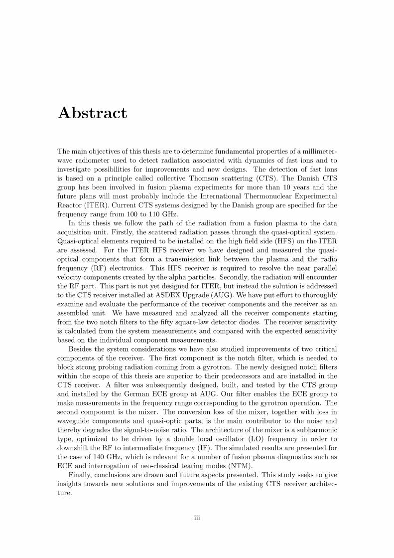
The still growing world population and its increasing social and business activities inalmost all regions of the world demand consumption of energy. In spite of the warn-ings from many independent energy research centers that humans rely heavily on energysources from fossil fuels, limited progress has been achieved towards sustainable energysources. However, the demand for more energy is increasing all over the world with high-est growth rates in the fast developing countries known as BRIC (Brazil, Russia, Indiaand China). Figure 1.1 shows consumption of energy in the World as function of time.In the years from 1990 to 2008 we have observed an increased consumption of all energysources, especially coal and oil. In the mean time, the production of nuclear fission energyhas the lowest growth rate, despite the fact that it is an energy source with no productionof greenhouse gases. In the years from 2008 to 2035 we see projections of possible energyconsumption showing growth in the consumption of all energy sources including fission.
Energy from oil, coal and similar fossil fuels are diminishing relatively fast which makesthem unfit for energy plans for future generations [61]. The best solution would be to havea sustainable energy source that could fulfill the energy consumption needs for all times.This is for sure not an easy task, but we have come closer to a solution. Fusion providesa safe solution to exploit an unlimited source of clean energy. This thesis is dedicatedto the design of microwave components used in diagnostic systems for analysis of fusionplasmas and hopefully provides a small step in human kind’s fusion energy quest.
1.1 Thermonuclear energy
The main objective in fusion science is to copy the source of energy that exists in the Sunand stars across the Universe here on Earth. In a fusion process two light atomic nucleifuse together to create a heavier nucleus. During this process a large portion of energy isreleased as electromagnetic radiation and fast particles. The basic physics behind fusionhas been known for more than 70 years, but despite a lot of research work during last50 years we still do not have a functional reactor that produces energy using controlledfusion. However, we know that fusion is possible, i.e. we feel joy of fusion every dayin form of electromagnetic radiation from the Sun, but the questions are what physicalcircumstances and which technical aspects do we need to fulfil before we can achievecontrolled fusion reactions here on Earth.
A fusion reactor is analogous to an old fashioned oven where coal and woodchips areused as fuel to produce energy. In such an oven, when the temperature is sufficiently high,combustion processes are started, and carbon and hydrogen atoms make chemical boundsto oxygen to produce carbon dioxide, water and heat. A part of the produced energy will
1
PhD Thesis Chapter 1. Introduction
1990 2000 2008 2015 2025 20350
50
100
150
200
250
Year
Qua
ds
OilGasCoalFissionRenewable
Figure 1.1: Consumption of energy divided into 5 different sources using data from U.S. EnergyInformation Administration. The unit for large quantity of energy is called “Quad”where 1 Quad = 1.055 · 1018 Joules = 25, 200, 000 Tonnes of oil. Renewable energycomes from natural resources such as sunlight, wind, tides, and geothermal heat.
also heat up the surrounding fuel so that the process becomes self-sustained for a longerperiod of time. In this combustion process only electron clouds of atom nuclei interactwith each other, while nuclei itself are unaffected. Therefore, these reactions are relativelyeasy to sustain, and the ignition temperature is relatively low, i.e. most mixtures igniteat around 1000 oC.
In fusion reactors principles from the combustion oven remain the same but the physicsis different. The fuel is a mixture of two isotopes of light atomic nuclei, deuterium andtritium. Both gases are heated up in a closed chamber; the gases get ionized and fromthis point we simply use term plasma to describe the hot mixture of ionized gases. Atsufficiently high temperature and density, fusion reactions initiate and a part of the energyproduced by fusion will remain in the plasma to self-sustain the ignited fusion reactions,i.e. no external heat sources are needed.
The temperature needed to start the chain of fusion reactions is around 100 million oC.High temperatures of that order raise a lot of technical challenges such as finding heatsources that are powerful and are able to couple large amount of their available powerto plasma and building a fusion reactor that can contain these extremely hot plasmas.Besides that the fusion plasmas should not be in direct contact with surrounding wallsor otherwise the plasma will immediately cool down and all the fusion chain reactionswill stop. For the last several decades there have been developed methods for successfulheating of the plasma beyond 100 million oC, while plasma containment is still a challengewe face and are obliged to solve. The difficulties with plasma containment is widelyaddressed in the fusion community and will hopefully be solved in the near future. Atthat time we will have a first prototype of fusion reactor, and we will be very close to asource of sustainable energy. The future generations will have an alternative eco-friendlyenergy source that is free of production of carbon dioxide and similar greenhouse gasescreated from the combustion of fossil fuels.
Several large projects on fusion energy have been started around the world such as the“Tokamak Fusion Test Reactor” (TFTR) in US, “Tokamak Experiment for TechnologyOriented Research” (TEXTOR) in Germany, “Joint European Torus” (JET) in Culham,Great Britain, “Axially Symmetric Divertor EXperiment” (ASDEX) Upgrade in Germanyand the future machine “International Thermonuclear Experimental Reactor” (ITER) in
V.Furtula 2

PhD Thesis Chapter 1. Introduction
South France. ITER will be the largest tokamak in the world, a gate to understand fusionplasma containment in detail. So, what do we expect to get in 30-40 years from ITERand the research effort and financial investments in fusion science? We expect to buildfusion reactors that will
• give us an inexhaustible amount of energy since the fuels are easily accessible innature.
• produce eco-friendly energy and save the environment from harmful waste productssuch as carbon dioxide, dangerous chemicals and radioactive materials.
• be able to produce energy for a compatible price relative to energy production pricebased on fossil fuels or nuclear fission.
Before we can achieve these goals, political organizations and educational institutionsmust provide necessary resources to the field of fusion science. Fortunately, the motivationfor fusion among scientists is strong and the last decade’s progress in fusion research hasincreased public confidence that fusion is possible here on Earth. During next few sectionswe will get familiar with basic concepts behind fusion.
1.2 Thermonuclear Fusion
Plasma is often referred to as the fourth state of matter, in which a gas may be fullyor partially ionized, i.e. at least one electron is repelled from the electron cloud of therespective atom nucleus. In general terms, we identify as plasma any state of matter thatcontains enough free charged particles so its dynamics is dominated by electromagneticforces. We need very small portion of gas to be ionized before the dynamics exhibitelectromagnetic properties, for instance 0.1 percent ionization of a gas results in electricalconductivity almost half of the maximum possible.
Plasma dynamics is described by the self-consistent interaction between electromag-netic fields, governed by Maxwell’s equations, and spatial resolution of a large amount ofcharged particles, governed by the Lorentz equation. In other words, given the instanta-neous electric and magnetic fields E(x, t) and B(x, t), the forces on the particle j can becalculated using the Lorentz equation and then iteratively used to update the path xj(t)and velocity vj(t) of each particle. This procedure is, however, completely impossible tohandle for computers of many years to come. The number of particles even in a singleDebye sphere, i.e. a sphere with a radius of one Debye length, is just too large. Thefollowing three parameters are widely used to characterize a plasma:
1. the particle density n of each particle species measured in particles per cubic meter,
2. the temperature T of each particle species measured in eV,
3. the steady-state magnetic field B measured in Tesla, in the case plasma is confinedby surrounding magnetic field.
The most common investigated fusion reactions are applied on light gases such asdeuterium and tritium. Following three reactions may be used as a basis for design offusion plasmas containment chambers
V.Furtula 3
PhD Thesis Chapter 1. Introduction
21H + 2
1H −→
31H + 1
1H 50%32He+
10n 50%
(1.1)
21H + 3
1H −→ 42He+
10n (17.6MeV ) (1.2)
21H + 3
2He −→ 42He+
11p (1.3)
The energy output of deuterium-tritium (D-T) reaction is ∆E = 17.6 MeV from which3.5 MeV is associated with the alpha particle 4
2He and 14.1 MeV is associated with theneutron 1
0n. Thereby, one fifth of the net energy gained from a D-T reaction is carriedby the alpha particle while four fifth is carried by the neutron. The alpha particle isconfined by the magnetic field that contains plasma and is used to heat the plasma in thebackground, i.e. the bulk plasma. The neutron carries no electric charge, and therefore itcan pass the magnetic field lines and has to be absorbed by the surrounding wall blankets.
The D-T fuel cycle is, due to the low cross section described in Sec. 1.2.1, easiest andmost promising fusion reaction to be used for fusion experiments. Deuterium is foundin relatively large scales in the seawater while tritium is unstable and does not occurnaturally. Therefore, D-T fuel cycle requires breeding of the tritium from e.g. lithiumthrough one of the following reactions
63Li +
10n −→ 3
1T+ 42He, (1.4)
73Li +
10n −→ 3
1T+ 42He +
10n (1.5)
Preliminary calculations show that a 1 GW fusion power plant requires an annual D-Tfuel consumption of 250 kg. D-T fuel required for continuous burning plasma in a 1 GWfusion power plant is few grams, implying that we have maximum some grams of D-Tfuel in the power plant at all times. Therefore, safety is never compromised as it wouldbe the case for a fission power plant.
1.2.1 The Lawson Criterion
In plasma physics it is convenient to use the electronvolt [eV] as a normalized unit oftemperature, so that 1 eV is approximately 11600 Kelvin (K) due to the conversion1 · q
kB= 11604.5 K where kB is the Boltzmann constant and q is the electron charge. The
fusion energy generated by a D-T reaction is calculated as Pfusion = nDnT < σv > ∆E,where nD and nT are densities of deuterium and tritium, respectively, and < σv >denotes the reaction rate, σ being the collisional cross-section and v the relative velocityof colliding particles. For a D-T plasma with reaction temperature of 10 keV, we find< σv >∼ 1.1 · 10−23 [m3s−1] so that Pfusion ∼ 7.7 · 10−35n2 [Wm−3]. About 20% of thisoutput is the kinetic energy associated with alpha particles which is available to sustainthe process of fusion in the reactor chamber while the remaining 80% is kinetic energy ofthe neutrons which escape from the plasma to the surrounding wall blankets. Thus, theenergy absorbed by the plasma is Pα = nDnT < σv > Eα, where Eα = 3.5 MeV. Pα isthe heating power that is added to the unit volume of plasma per unit time caused byfusion. The reaction rate at temperatures of the order of 10 keV, corresponding to thetemperature of 116 million K which are achievable and containable in nowadays plasmaexperiments, is sufficient for fusion to occur. If we assume nD = nT = ne/2, where ne isthe electron density, the fusion power density becomes
Pfusion =1
4n2e < σv > Efusion. (1.6)
V.Furtula 4

PhD Thesis Chapter 1. Introduction
The fusion gain factor Q is analogous to the quality factor of an electric circuit, i.e. aratio of internal and external sources
Q =Pfusion
Paux
, (1.7)
where Paux is, in many cases, a sum of several independent auxiliary heating sources. Forthe case Q = 1 is called break-even and Q = ∞ ignition. For the case the break-even pointis surpassed, i.e. Q > 1, we call this condition for burning plasma. In 1997 researchersat JET reached fusion gain factor of Q = 0.64. Preliminary calculations show that thegain factor Q > 5 implies that the fusion power delivered to the absorbing blankets isgreater than the external heating power. ITER, the new but not yet built device basedon magnetic confinement, has the goal to reach Q = 10. Achieving a gain factor aboveQ = 20 is considered as good as ignition. This number will most probably not be reachedin ITER, and we may have to go for another version of a fusion power plant in order toreach ignition.
The energy loss from the plasma is calculated using the energy confinement time τEand the energy stored in the plasma 3neT
Ploss =3neT
τE(1.8)
The power generated by the fusion reactions and the power delivered to heat the plasmais calculated as
Pin = Pfusion + Paux = Pfusion +Pfusion
Paux, (1.9)
= Pfusion
(
1 +1
Q
)
. (1.10)
Now, we can derive the Lawson criterion through the statement that the input powershould be (at least) as large as the power loss. Thus we have
Pin ≥ Ploss ⇒ (1.11)(
1 +1
Q
)
n2e4< σv > Efusion ≥ 3neT
τE⇒ (1.12)
neTτE ≥ Q
Q+ 1
12
Efusion
T 2
< σv >. (1.13)
When the Lawson criterion is written as in Eq. (1.13) it is called “the triple” productsince it uses density, temperature, and confinement time to determine the figure of meritfor a plasma, a state where ignition is reached. Put differently, we need to find a scenarioin this four-dimensional space (3 independent parameters and the product) so heating ofthe plasma by means of fusion is sufficient to maintain the temperature of the plasmaagainst all losses without use of external sources. In the case that we have ignition, i.e.Q = ∞, then for a D-T reaction we get from Lawson criterion neTτE > 1020 keV s/m−3.
1.3 The Tokamak
The fusion energy we intent to produce here on Earth seems to have best burning con-ditions in a chamber called tokamak. The tokamak is a toroidal device, shaped as a
V.Furtula 5
PhD Thesis Chapter 1. Introduction
R
R0 θr
a b
Z
φ
zZ
φ
R0
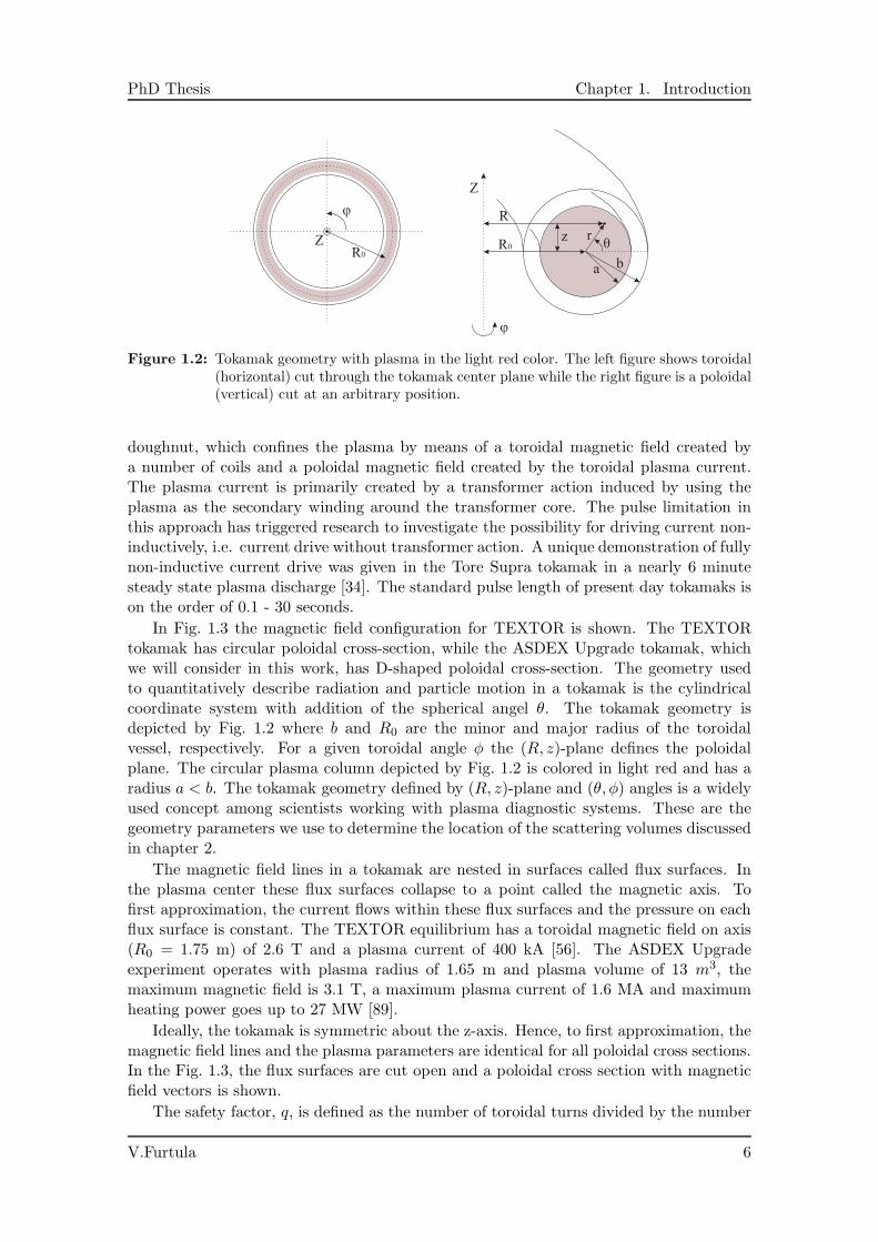
Figure 1.2: Tokamak geometry with plasma in the light red color. The left figure shows toroidal(horizontal) cut through the tokamak center plane while the right figure is a poloidal(vertical) cut at an arbitrary position.
doughnut, which confines the plasma by means of a toroidal magnetic field created bya number of coils and a poloidal magnetic field created by the toroidal plasma current.The plasma current is primarily created by a transformer action induced by using theplasma as the secondary winding around the transformer core. The pulse limitation inthis approach has triggered research to investigate the possibility for driving current non-inductively, i.e. current drive without transformer action. A unique demonstration of fullynon-inductive current drive was given in the Tore Supra tokamak in a nearly 6 minutesteady state plasma discharge [34]. The standard pulse length of present day tokamaks ison the order of 0.1 - 30 seconds.
In Fig. 1.3 the magnetic field configuration for TEXTOR is shown. The TEXTORtokamak has circular poloidal cross-section, while the ASDEX Upgrade tokamak, whichwe will consider in this work, has D-shaped poloidal cross-section. The geometry usedto quantitatively describe radiation and particle motion in a tokamak is the cylindricalcoordinate system with addition of the spherical angel θ. The tokamak geometry isdepicted by Fig. 1.2 where b and R0 are the minor and major radius of the toroidalvessel, respectively. For a given toroidal angle φ the (R, z)-plane defines the poloidalplane. The circular plasma column depicted by Fig. 1.2 is colored in light red and has aradius a < b. The tokamak geometry defined by (R, z)-plane and (θ, φ) angles is a widelyused concept among scientists working with plasma diagnostic systems. These are thegeometry parameters we use to determine the location of the scattering volumes discussedin chapter 2.
The magnetic field lines in a tokamak are nested in surfaces called flux surfaces. Inthe plasma center these flux surfaces collapse to a point called the magnetic axis. Tofirst approximation, the current flows within these flux surfaces and the pressure on eachflux surface is constant. The TEXTOR equilibrium has a toroidal magnetic field on axis(R0 = 1.75 m) of 2.6 T and a plasma current of 400 kA [56]. The ASDEX Upgradeexperiment operates with plasma radius of 1.65 m and plasma volume of 13 m3, themaximum magnetic field is 3.1 T, a maximum plasma current of 1.6 MA and maximumheating power goes up to 27 MW [89].
Ideally, the tokamak is symmetric about the z-axis. Hence, to first approximation, themagnetic field lines and the plasma parameters are identical for all poloidal cross sections.In the Fig. 1.3, the flux surfaces are cut open and a poloidal cross section with magneticfield vectors is shown.
The safety factor, q, is defined as the number of toroidal turns divided by the number
V.Furtula 6
PhD Thesis Chapter 1. Introduction
coils wound around torusto produce toroidalmagnetic field
transformerwinding(primary circuit)
poloidalmagnetic fieldB
θ
toroidalmagnetic fieldBφ helical field
plasma particles contained bymagnetic field
iron transformer core
plasma current I(secondary circuit)
p
Ro
main axis
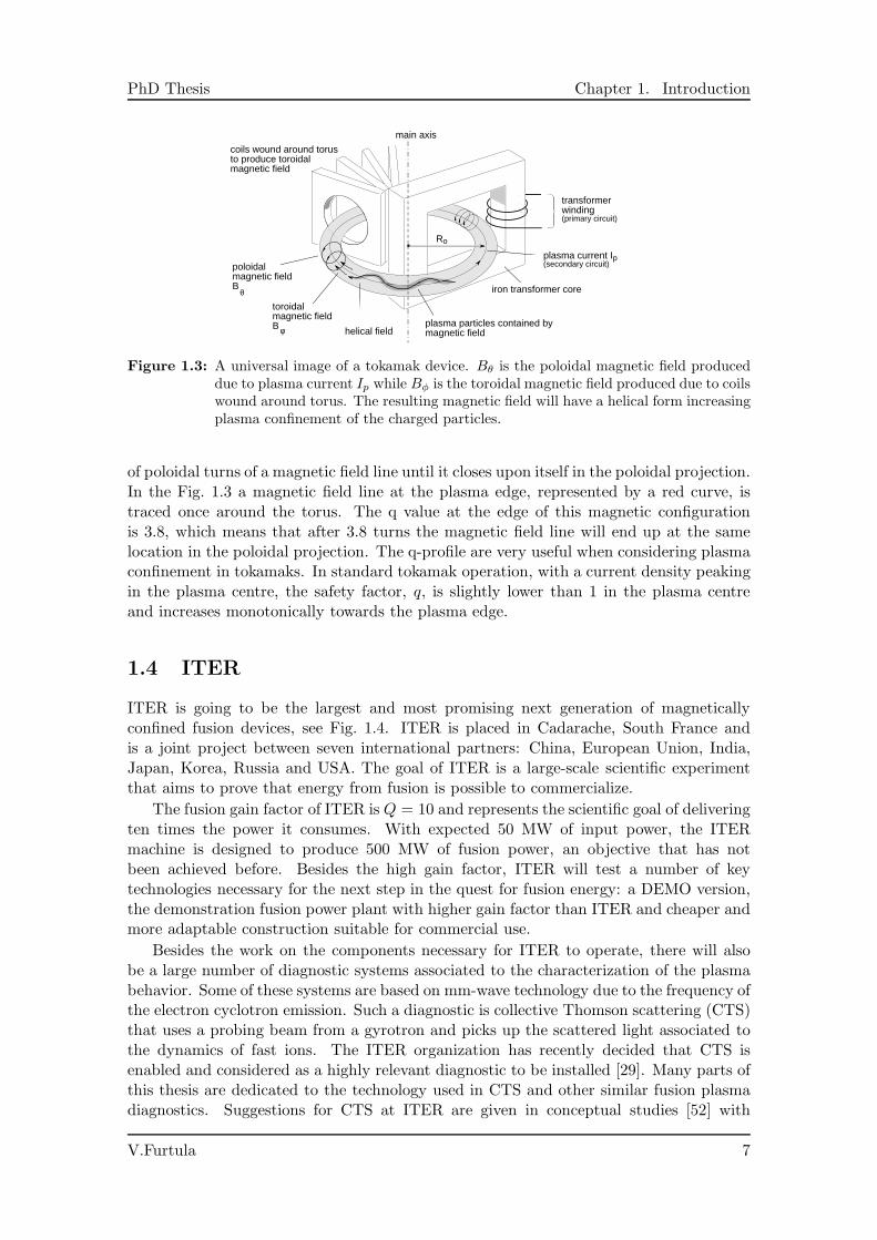
Figure 1.3: A universal image of a tokamak device. Bθ is the poloidal magnetic field produceddue to plasma current Ip while Bφ is the toroidal magnetic field produced due to coilswound around torus. The resulting magnetic field will have a helical form increasingplasma confinement of the charged particles.
of poloidal turns of a magnetic field line until it closes upon itself in the poloidal projection.In the Fig. 1.3 a magnetic field line at the plasma edge, represented by a red curve, istraced once around the torus. The q value at the edge of this magnetic configurationis 3.8, which means that after 3.8 turns the magnetic field line will end up at the samelocation in the poloidal projection. The q-profile are very useful when considering plasmaconfinement in tokamaks. In standard tokamak operation, with a current density peakingin the plasma centre, the safety factor, q, is slightly lower than 1 in the plasma centreand increases monotonically towards the plasma edge.
1.4 ITER
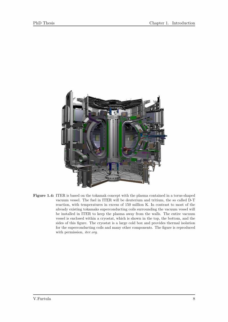
ITER is going to be the largest and most promising next generation of magneticallyconfined fusion devices, see Fig. 1.4. ITER is placed in Cadarache, South France andis a joint project between seven international partners: China, European Union, India,Japan, Korea, Russia and USA. The goal of ITER is a large-scale scientific experimentthat aims to prove that energy from fusion is possible to commercialize.
The fusion gain factor of ITER is Q = 10 and represents the scientific goal of deliveringten times the power it consumes. With expected 50 MW of input power, the ITERmachine is designed to produce 500 MW of fusion power, an objective that has notbeen achieved before. Besides the high gain factor, ITER will test a number of keytechnologies necessary for the next step in the quest for fusion energy: a DEMO version,the demonstration fusion power plant with higher gain factor than ITER and cheaper andmore adaptable construction suitable for commercial use.
Besides the work on the components necessary for ITER to operate, there will alsobe a large number of diagnostic systems associated to the characterization of the plasmabehavior. Some of these systems are based on mm-wave technology due to the frequency ofthe electron cyclotron emission. Such a diagnostic is collective Thomson scattering (CTS)that uses a probing beam from a gyrotron and picks up the scattered light associated tothe dynamics of fast ions. The ITER organization has recently decided that CTS isenabled and considered as a highly relevant diagnostic to be installed [29]. Many parts ofthis thesis are dedicated to the technology used in CTS and other similar fusion plasmadiagnostics. Suggestions for CTS at ITER are given in conceptual studies [52] with
V.Furtula 7
PhD Thesis Chapter 1. Introduction
Figure 1.4: ITER is based on the tokamak concept with the plasma contained in a torus-shapedvacuum vessel. The fuel in ITER will be deuterium and tritium, the so called D-Treaction, with temperatures in excess of 150 million K. In contrast to most of thealready existing tokamaks superconducting coils surrounding the vacuum vessel willbe installed in ITER to keep the plasma away from the walls. The entire vacuumvessel is enclosed within a cryostat, which is shown in the top, the bottom, and thesides of this figure. The cryostat is a large cold box and provides thermal isolationfor the superconducting coils and many other components. The figure is reproducedwith permission, iter.org.
V.Furtula 8

PhD Thesis Chapter 1. Introduction
scattering geometry described in Sec. 2.4.
V.Furtula 9

Chapter 2
Collective Thomson Scattering
2.1 Short background and introduction
The conditions for operating a diagnostic for fusion plasmas are, due to strongly radiativeenvironment, relatively complicated and require careful attention to the hardware. Dueto the harsh environment of the plasmas all contact diagnostics fail to survive in suchdifficult and hostile conditions. Otherwise temperature, density and even the distributionfunction of the charged particles could be measured by probes. Necessity of using elec-tromagnetic radiation to characterize dynamics of charged particles, taking into accountthe technologies available for diagnostics, is inevitable. The electromagnetic radiationdue to scattering off electrons is an important diagnostic in fusion as in other fields ofphysics dealing with charged particles. This chapter is intended as an introduction to theprinciple of CTS with a short description of the CTS diagnostic.
When charged particles are affected by an electric field they get accelerated and asa consequence radiation is emitted. Assuming that the charged particle is acceleratedto some velocity ∆v ≪ c, then according to Larmor’s equation [10] the radiated powerscales as the acceleration squared multiplied by charge square. During scattering experi-ments in plasmas, the radiation from the probing beam accelerates both the ions and theelectrons. Since the ions are much heavier than the electrons, and the magnitude of theacceleration is inversely proportional to the mass, the radiation emitted from the ions canbe neglected. Thomson scattering is electromagnetic scattering off electrons not boundby atomic states. Due to the Doppler shift, scattered radiation off uncorrelated electronscontains information on electron dynamics such as thermal motion and hence the electrontemperature. At higher densities the electron correlations are not negligible. Here, weassume an incident wave which scatters off fluctuations in the electron distribution. Inplasmas, the electric field produced by a given test particle is screened by the electro-magnetic fields emitted by the electrons. The length scale of this screening is usuallydescribed by a sphere with a radius λD called Debye length
λD =
√
ǫ0Teneq2e
, (2.1)
where subscript Te is electron temperature, ne is electron density, and qe is elementarycharge. In a tokamak the Debye length is typically few millimeters, while in the Solarcore the Debye length is in the nanometer range due to very high densities. In thecase where the resolved fluctuation scale length is much smaller than the Debye length,the assumption on uncorrelated electrons is sufficient to describe the scattering process.
11
PhD Thesis Chapter 2. Collective Thomson Scattering
Resolved plasmafluctuation
Received scatteredradiation
k s
k i
kd
Incident radiation
ReceiverProbe
= k - k
ks
k i
kd
s ik
d
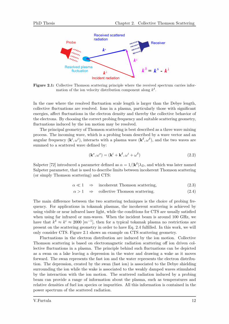
Figure 2.1: Collective Thomson scattering principle where the received spectrum carries infor-mation of the ion velocity distribution component along kδ.
In the case where the resolved fluctuation scale length is larger than the Debye length,collective fluctuations are resolved. Ions in a plasma, particularly those with significantenergies, affect fluctuations in the electron density and thereby the collective behavior ofthe electrons. By choosing the correct probing frequency and suitable scattering geometry,fluctuations induced by the ion motion may be resolved.
The principal geometry of Thomson scattering is best described as a three wave mixingprocess. The incoming wave, which is a probing beam described by a wave vector and anangular frequency (ki, ωi), interacts with a plasma wave (kδ, ωδ), and the two waves aresummed to a scattered wave defined by:
(ks, ωs) = (ki + kδ, ωi + ωδ) (2.2)
Salpeter [72] introduced a parameter defined as α = 1/|kδ |λD, and which was later namedSalpeter parameter, that is used to describe limits between incoherent Thomson scattering(or simply Thomson scattering) and CTS:
α≪ 1 ⇒ incoherent Thomson scattering, (2.3)
α > 1 ⇒ collective Thomson scattering. (2.4)
The main difference between the two scattering techniques is the choice of probing fre-quency. For applications in tokamak plasmas, the incoherent scattering is achieved byusing visible or near infrared laser light, while the conditions for CTS are usually satisfiedwhen using far infrared or mm-waves. When the incident beam is around 100 GHz, wehave that kδ ≈ ki ≈ 2000 [m−1], then for a typical tokamak plasma no restrictions arepresent on the scattering geometry in order to have Eq. 2.4 fulfilled. In this work, we willonly consider CTS. Figure 2.1 shows an example on CTS scattering geometry.
Fluctuations in the electron distribution are induced by the ion motion. CollectiveThomson scattering is based on electromagnetic radiation scattering off ion driven col-lective fluctuations in a plasma. The principle behind such fluctuations can be depictedas a swan on a lake leaving a depression in the water and drawing a wake as it movesforward. The swan represents the fast ion and the water represents the electron distribu-tion. The depression, created by the swan (fast ion) is associated to the Debye shieldingsurrounding the ion while the wake is associated to the weakly damped waves stimulatedby the interaction with the ion motion. The scattered radiation induced by a probingbeam can provide a range of information about the plasma, such as temperatures andrelative densities of fuel ion species or impurities. All this information is contained in thepower spectrum of the scattered radiation.
V.Furtula 12
PhD Thesis Chapter 2. Collective Thomson Scattering
2.2 Example of a CTS spectrum
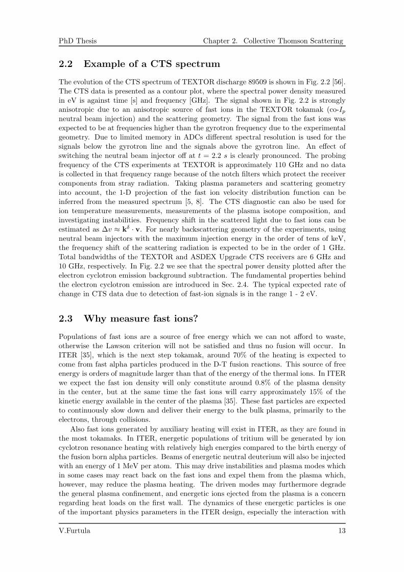
The evolution of the CTS spectrum of TEXTOR discharge 89509 is shown in Fig. 2.2 [56].The CTS data is presented as a contour plot, where the spectral power density measuredin eV is against time [s] and frequency [GHz]. The signal shown in Fig. 2.2 is stronglyanisotropic due to an anisotropic source of fast ions in the TEXTOR tokamak (co-Ipneutral beam injection) and the scattering geometry. The signal from the fast ions wasexpected to be at frequencies higher than the gyrotron frequency due to the experimentalgeometry. Due to limited memory in ADCs different spectral resolution is used for thesignals below the gyrotron line and the signals above the gyrotron line. An effect ofswitching the neutral beam injector off at t = 2.2 s is clearly pronounced. The probingfrequency of the CTS experiments at TEXTOR is approximately 110 GHz and no datais collected in that frequency range because of the notch filters which protect the receivercomponents from stray radiation. Taking plasma parameters and scattering geometryinto account, the 1-D projection of the fast ion velocity distribution function can beinferred from the measured spectrum [5, 8]. The CTS diagnostic can also be used forion temperature measurements, measurements of the plasma isotope composition, andinvestigating instabilities. Frequency shift in the scattered light due to fast ions can beestimated as ∆v ≈ kδ · v. For nearly backscattering geometry of the experiments, usingneutral beam injectors with the maximum injection energy in the order of tens of keV,the frequency shift of the scattering radiation is expected to be in the order of 1 GHz.Total bandwidths of the TEXTOR and ASDEX Upgrade CTS receivers are 6 GHz and10 GHz, respectively. In Fig. 2.2 we see that the spectral power density plotted after theelectron cyclotron emission background subtraction. The fundamental properties behindthe electron cyclotron emission are introduced in Sec. 2.4. The typical expected rate ofchange in CTS data due to detection of fast-ion signals is in the range 1 - 2 eV.
2.3 Why measure fast ions?
Populations of fast ions are a source of free energy which we can not afford to waste,otherwise the Lawson criterion will not be satisfied and thus no fusion will occur. InITER [35], which is the next step tokamak, around 70% of the heating is expected tocome from fast alpha particles produced in the D-T fusion reactions. This source of freeenergy is orders of magnitude larger than that of the energy of the thermal ions. In ITERwe expect the fast ion density will only constitute around 0.8% of the plasma densityin the center, but at the same time the fast ions will carry approximately 15% of thekinetic energy available in the center of the plasma [35]. These fast particles are expectedto continuously slow down and deliver their energy to the bulk plasma, primarily to theelectrons, through collisions.
Also fast ions generated by auxiliary heating will exist in ITER, as they are found inthe most tokamaks. In ITER, energetic populations of tritium will be generated by ioncyclotron resonance heating with relatively high energies compared to the birth energy ofthe fusion born alpha particles. Beams of energetic neutral deuterium will also be injectedwith an energy of 1 MeV per atom. This may drive instabilities and plasma modes whichin some cases may react back on the fast ions and expel them from the plasma which,however, may reduce the plasma heating. The driven modes may furthermore degradethe general plasma confinement, and energetic ions ejected from the plasma is a concernregarding heat loads on the first wall. The dynamics of these energetic particles is oneof the important physics parameters in the ITER design, especially the interaction with
V.Furtula 13
PhD Thesis Chapter 2. Collective Thomson Scattering
Figure 2.2: A typical contour plot of CTS spectral power density reprinted with permission [56].In (a) the ion heating is turned off at t = 2.2 s consequently decreasing the widthof the CTS spectrum. The CTS spectrum at t = 2.3 s (heating off) is shown in (b)while that at t = 2.1 s (during heating flattop) is shown in (c).
V.Furtula 14
PhD Thesis Chapter 2. Collective Thomson Scattering
MOU #2MOU #1
Gyrotron #1
Platform forGyrotron #2
CTS-AUGreceiver
Figure 2.3: Overview of the gyrotron hall at ASDEX Upgrade.
instabilities, in order to avoid scenarios where fast ions are lost. Further development andsuccessful experimental measurements, through reliable diagnostics such as CTS, of fastions resolved in time, space and velocity are needed.
2.4 CTS systems today and in future
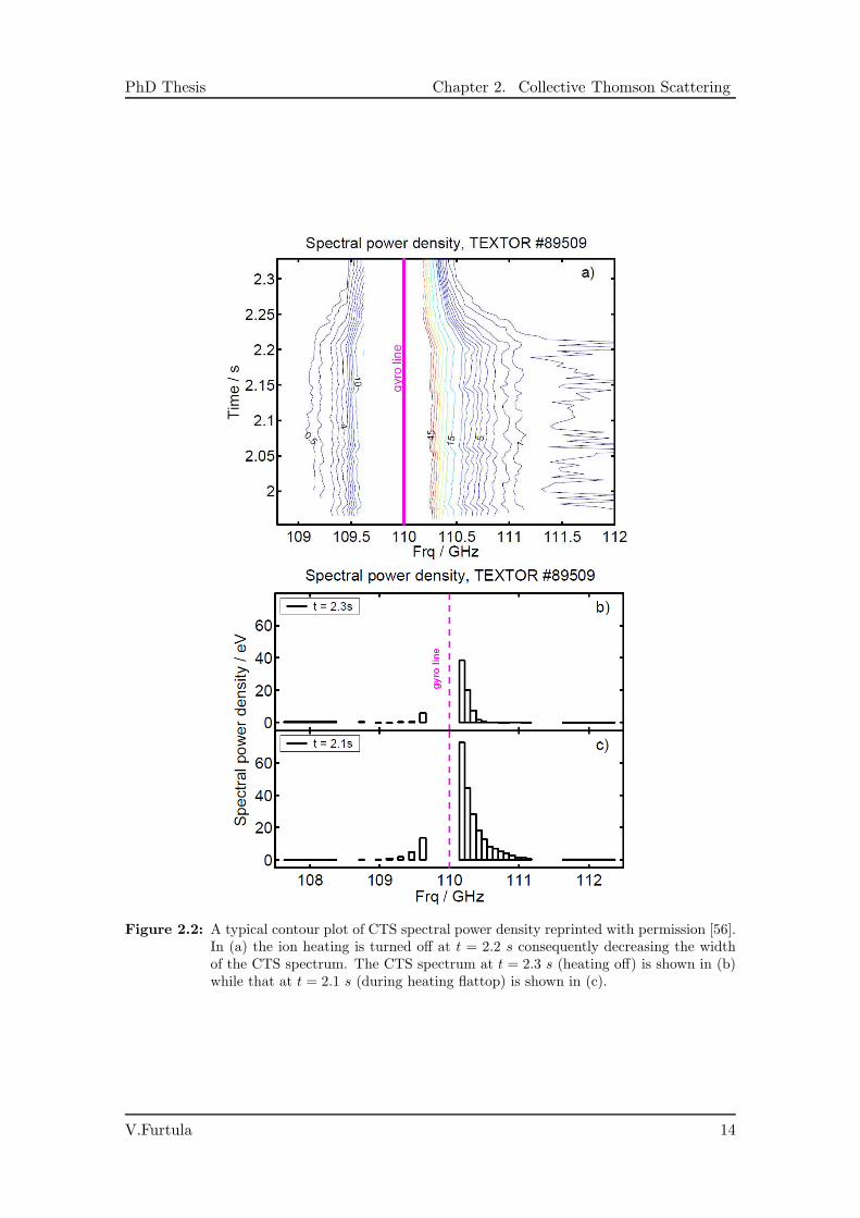
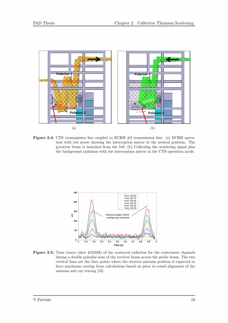
At ASDEX Upgrade, Garching, Germany, a fully equipped CTS system is in operation.The front-end electronic part of the receiver is placed inside the gyrotron hall due toflexible access of the receiving beam. The gyrotron hall together with the CTS receiveris shown in Fig. 2.3 where we also see matching optics unit (MOU) boxes relatively closeto the receiver. The MOU is a large, enclosed aluminium box that contains quasi-opticcomponents for beam shaping, polarization selection, and calorimetric measurements.Figure 2.4 shows the inside an MOU box in two operating modes; gyrotron mode and theCTS mode which is governed by a movable mirrors that intercepts the incoming signalinto the CTS receiver, as shown in Fig. 2.4(b).
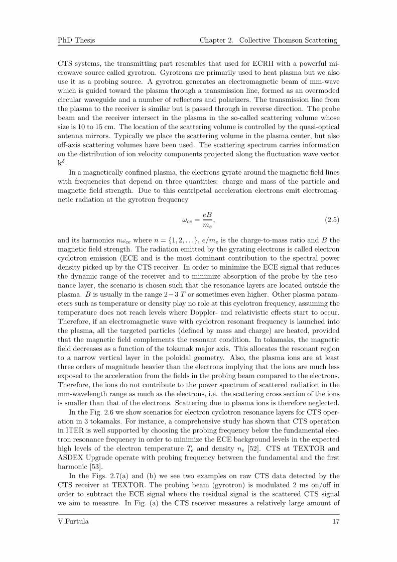
The maximum signal will occur at particular mirror angles according to the ray trac-ing calculations under assumption that the alignment of the polarizers and mirrors isperformed correctly. This is shown in Fig. 2.5.
CTS can provide spatially and temporally resolved measurements of the one-dimensional(1-D) fast-ion velocity distribution along the direction of kδ vector which is determinedby the scattering geometry. The components of the kδ vector are defined with respect tothe direction of the magnetic field B, and thus the fast-ion distribution may be measuredas a function of velocity parallel or perpendicular to B. For fusion plasmas, measureddistributions are a sum of alpha and other fast ions distributions where each populationis weighted by the square of the species charge. CTS technique has successfully providedspatially and temporally resolved measurements of the one-dimensional fast ion veloc-ity distribution on JET [6]. Also a range of successful fast ion measurements has beendemonstrated in TEXTOR [56, 8, 57, 58, 59]. Promising and still on-going work on fastion data at ASDEX Upgrade has been demonstrated [53, 54, 42].
The CTS hardware consists of a transmitting and receiving part. In microwave based
V.Furtula 15
PhD Thesis Chapter 2. Collective Thomson Scattering
Polarizer 1
Polarizer 2
(a)
Polarizer 1
Polarizer 2
(b)
Figure 2.4: CTS transmission line coupled to ECRH #2 transmission line: (a) ECRH opera-tion with red arrow showing the interception mirror in the neutral position. Thegyrotron beam is launched from the left; (b) Collecting the scattering signal plusthe background radiation with the interception mirror in the CTS operation mode.
2 2.1 2.2 2.3 2.4 2.5 2.6 2.7 2.8 2.9 30
50
100
150
200
250
Time [s]
eV
Freq: 104.65Freq: 104.75Freq: 104.85Freq: 105.25Freq: 105.35Freq: 105.45
Antenna angles where overlap was expected
Figure 2.5: Time traces (shot #22328) of the scattered radiation for the centermost channelsduring a double poloidal scan of the receiver beam across the probe beam. The twovertical lines are the time points where the receiver antenna position is expected tohave maximum overlap from calculations based on prior in-vessel alignment of theantenna and ray tracing [53].
V.Furtula 16
PhD Thesis Chapter 2. Collective Thomson Scattering
CTS systems, the transmitting part resembles that used for ECRH with a powerful mi-crowave source called gyrotron. Gyrotrons are primarily used to heat plasma but we alsouse it as a probing source. A gyrotron generates an electromagnetic beam of mm-wavewhich is guided toward the plasma through a transmission line, formed as an overmodedcircular waveguide and a number of reflectors and polarizers. The transmission line fromthe plasma to the receiver is similar but is passed through in reverse direction. The probebeam and the receiver intersect in the plasma in the so-called scattering volume whosesize is 10 to 15 cm. The location of the scattering volume is controlled by the quasi-opticalantenna mirrors. Typically we place the scattering volume in the plasma center, but alsooff-axis scattering volumes have been used. The scattering spectrum carries informationon the distribution of ion velocity components projected along the fluctuation wave vectorkδ.
In a magnetically confined plasma, the electrons gyrate around the magnetic field lineswith frequencies that depend on three quantities: charge and mass of the particle andmagnetic field strength. Due to this centripetal acceleration electrons emit electromag-netic radiation at the gyrotron frequency
ωce =eB
me
, (2.5)
and its harmonics nωce where n = 1, 2, . . ., e/me is the charge-to-mass ratio and B themagnetic field strength. The radiation emitted by the gyrating electrons is called electroncyclotron emission (ECE and is the most dominant contribution to the spectral powerdensity picked up by the CTS receiver. In order to minimize the ECE signal that reducesthe dynamic range of the receiver and to minimize absorption of the probe by the reso-nance layer, the scenario is chosen such that the resonance layers are located outside theplasma. B is usually in the range 2−3 T or sometimes even higher. Other plasma param-eters such as temperature or density play no role at this cyclotron frequency, assuming thetemperature does not reach levels where Doppler- and relativistic effects start to occur.Therefore, if an electromagnetic wave with cyclotron resonant frequency is launched intothe plasma, all the targeted particles (defined by mass and charge) are heated, providedthat the magnetic field complements the resonant condition. In tokamaks, the magneticfield decreases as a function of the tokamak major axis. This allocates the resonant regionto a narrow vertical layer in the poloidal geometry. Also, the plasma ions are at leastthree orders of magnitude heavier than the electrons implying that the ions are much lessexposed to the acceleration from the fields in the probing beam compared to the electrons.Therefore, the ions do not contribute to the power spectrum of scattered radiation in themm-wavelength range as much as the electrons, i.e. the scattering cross section of the ionsis smaller than that of the electrons. Scattering due to plasma ions is therefore neglected.
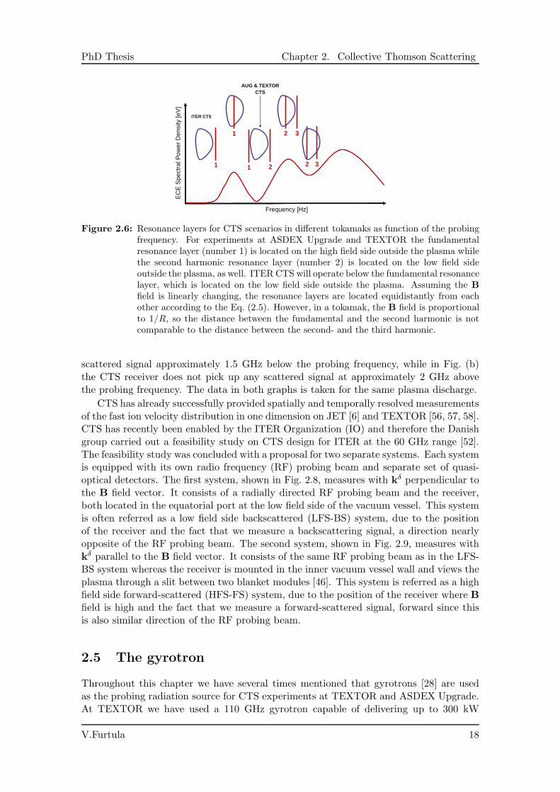
In the Fig. 2.6 we show scenarios for electron cyclotron resonance layers for CTS oper-ation in 3 tokamaks. For instance, a comprehensive study has shown that CTS operationin ITER is well supported by choosing the probing frequency below the fundamental elec-tron resonance frequency in order to minimize the ECE background levels in the expectedhigh levels of the electron temperature Te and density ne [52]. CTS at TEXTOR andASDEX Upgrade operate with probing frequency between the fundamental and the firstharmonic [53].
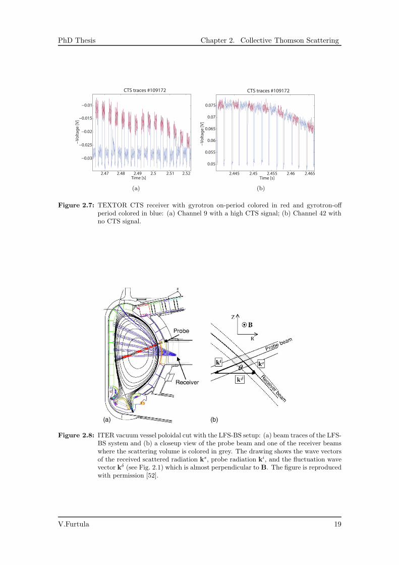
In the Figs. 2.7(a) and (b) we see two examples on raw CTS data detected by theCTS receiver at TEXTOR. The probing beam (gyrotron) is modulated 2 ms on/off inorder to subtract the ECE signal where the residual signal is the scattered CTS signalwe aim to measure. In Fig. (a) the CTS receiver measures a relatively large amount of
V.Furtula 17
PhD Thesis Chapter 2. Collective Thomson Scattering
EC
E S
pect
ralP
ower
Den
sity
[eV
]
Frequency [Hz]
11
11
11 22
22 33
22 33
ITER CTS
AUG & TEXTORCTS
Figure 2.6: Resonance layers for CTS scenarios in different tokamaks as function of the probingfrequency. For experiments at ASDEX Upgrade and TEXTOR the fundamentalresonance layer (number 1) is located on the high field side outside the plasma whilethe second harmonic resonance layer (number 2) is located on the low field sideoutside the plasma, as well. ITER CTS will operate below the fundamental resonancelayer, which is located on the low field side outside the plasma. Assuming the B
field is linearly changing, the resonance layers are located equidistantly from eachother according to the Eq. (2.5). However, in a tokamak, the B field is proportionalto 1/R, so the distance between the fundamental and the second harmonic is notcomparable to the distance between the second- and the third harmonic.
scattered signal approximately 1.5 GHz below the probing frequency, while in Fig. (b)the CTS receiver does not pick up any scattered signal at approximately 2 GHz abovethe probing frequency. The data in both graphs is taken for the same plasma discharge.
CTS has already successfully provided spatially and temporally resolved measurementsof the fast ion velocity distribution in one dimension on JET [6] and TEXTOR [56, 57, 58].CTS has recently been enabled by the ITER Organization (IO) and therefore the Danishgroup carried out a feasibility study on CTS design for ITER at the 60 GHz range [52].The feasibility study was concluded with a proposal for two separate systems. Each systemis equipped with its own radio frequency (RF) probing beam and separate set of quasi-optical detectors. The first system, shown in Fig. 2.8, measures with kδ perpendicular tothe B field vector. It consists of a radially directed RF probing beam and the receiver,both located in the equatorial port at the low field side of the vacuum vessel. This systemis often referred as a low field side backscattered (LFS-BS) system, due to the positionof the receiver and the fact that we measure a backscattering signal, a direction nearlyopposite of the RF probing beam. The second system, shown in Fig. 2.9, measures withkδ parallel to the B field vector. It consists of the same RF probing beam as in the LFS-BS system whereas the receiver is mounted in the inner vacuum vessel wall and views theplasma through a slit between two blanket modules [46]. This system is referred as a highfield side forward-scattered (HFS-FS) system, due to the position of the receiver where Bfield is high and the fact that we measure a forward-scattered signal, forward since thisis also similar direction of the RF probing beam.
2.5 The gyrotron
Throughout this chapter we have several times mentioned that gyrotrons [28] are usedas the probing radiation source for CTS experiments at TEXTOR and ASDEX Upgrade.At TEXTOR we have used a 110 GHz gyrotron capable of delivering up to 300 kW
V.Furtula 18
PhD Thesis Chapter 2. Collective Thomson Scattering
2.47 2.48 2.49 2.5 2.51 2.52
−0.03
−0.025
−0.02
−0.015
−0.01
Time [s]
−V
olt
ag
e [
V]
CTS traces #109172
(a)
2.445 2.45 2.455 2.46 2.465
0.05
0.055
0.06
0.065
0.07
0.075
CTS traces #109172
Time [s]
−V
olt
ag
e [
V]
(b)
Figure 2.7: TEXTOR CTS receiver with gyrotron on-period colored in red and gyrotron-offperiod colored in blue: (a) Channel 9 with a high CTS signal; (b) Channel 42 withno CTS signal.
Figure 2.8: ITER vacuum vessel poloidal cut with the LFS-BS setup: (a) beam traces of the LFS-BS system and (b) a closeup view of the probe beam and one of the receiver beamswhere the scattering volume is colored in grey. The drawing shows the wave vectorsof the received scattered radiation ks, probe radiation ki, and the fluctuation wavevector kδ (see Fig. 2.1) which is almost perpendicular to B. The figure is reproducedwith permission [52].
V.Furtula 19
PhD Thesis Chapter 2. Collective Thomson Scattering
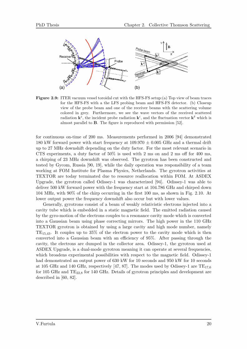
Figure 2.9: ITER vacuum vessel toroidal cut with the HFS-FS setup:(a) Top view of beam tracesfor the HFS-FS with a the LFS probing beam and HFS-FS detector. (b) Closeupview of the probe beam and one of the receiver beams with the scattering volumecolored in grey. Furthermore, we see the wave vectors of the received scatteredradiation ks, the incident probe radiation ki, and the fluctuation vector kδ which isalmost parallel to B. The figure is reproduced with permission [52].
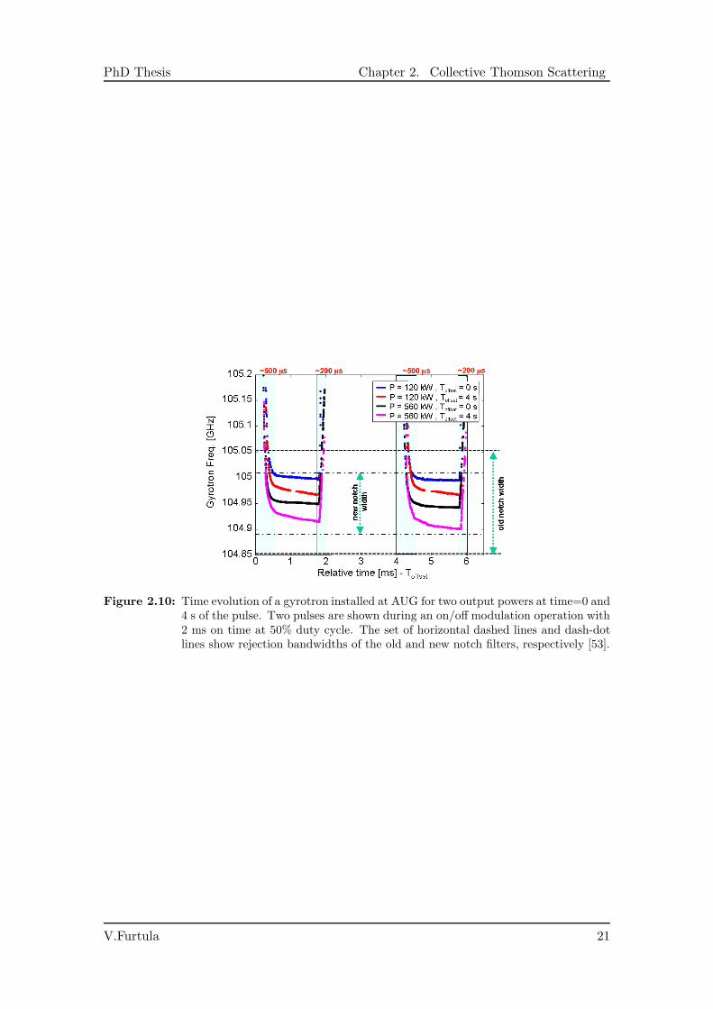
for continuous on-time of 200 ms. Measurements performed in 2006 [94] demonstrated180 kW forward power with start frequency at 109.970 ± 0.005 GHz and a thermal driftup to 27 MHz downshift depending on the duty factor. For the most relevant scenario inCTS experiments, a duty factor of 50% is used with 2 ms on and 2 ms off for 400 ms,a chirping of 23 MHz downshift was observed. The gyrotron has been constructed andtested by Gycom, Russia [90, 19], while the daily operation was responsibility of a teamworking at FOM Institute for Plasma Physics, Netherlands. The gyrotron activities atTEXTOR are today terminated due to resource reallocation within FOM. At ASDEXUpgrade, the gyrotron called Odissey-1 was characterized [94]. Odissey-1 was able todeliver 500 kW forward power with the frequency start at 104.786 GHz and chirped down104 MHz, with 90% of the chirp occurring in the first 100 ms, as shown in Fig. 2.10. Atlower output power the frequency downshift also occur but with lower values.
Generally, gyrotrons consist of a beam of weakly relativistic electrons injected into acavity tube which is embedded in a static magnetic field. The emitted radiation causedby the gyro-motion of the electrons couples to a resonance cavity mode which is convertedinto a Gaussian beam using phase correcting mirrors. The high power in the 110 GHzTEXTOR gyrotron is obtained by using a large cavity and high mode number, namelyTE15,43. It couples up to 35% of the electron power to the cavity mode which is thenconverted into a Gaussian beam with an efficiency of 95%. After passing through thecavity, the electrons are dumped in the collector area. Odissey-1, the gyrotron used atASDEX Upgrade, is a dual-mode gyrotron meaning it can operate at several frequencies,which broadens experimental possibilities with respect to the magnetic field. Odissey-1had demonstrated an output power of 630 kW for 10 seconds and 950 kW for 10 secondsat 105 GHz and 140 GHz, respectively [47, 87]. The modes used by Odissey-1 are TE17,6
for 105 GHz and TE22,8 for 140 GHz. Details of gyrotron principles and development aredescribed in [60, 82].
V.Furtula 20
PhD Thesis Chapter 2. Collective Thomson Scattering
Figure 2.10: Time evolution of a gyrotron installed at AUG for two output powers at time=0 and4 s of the pulse. Two pulses are shown during an on/off modulation operation with2 ms on time at 50% duty cycle. The set of horizontal dashed lines and dash-dotlines show rejection bandwidths of the old and new notch filters, respectively [53].
V.Furtula 21

Chapter 3
Millimeter wave Quasi-Optics forITER
3.1 Short background and introduction
A considerable amount of work in CTS group is dedicated to design of quasi-opticalcomponents. Due to the convenient integration possibilities and increased flexibility, thepath where CTS signal is backscattered to the electronic part of the receiver is physicallythe same as the path used for ECRH (RF heating) of the plasma. In other words,the existing ECRH sources set up a standard how quasi-optics should be designed forCTS experiments. Therefore, quasi-optics such as reflectors, polarizers, and waveguidetransmissions are similar in size and shape for both CTS and ECRH. This chapter isintended to give an impression how quasi-optical reflectors for millimeter-wave diagnostics,installed at fusion devices, are constructed and tested.
The quasi optics is the first part of the front-end hardware electromagnetic radiation,coming from a plasma, encounters on its way to the receiver. Therefore any losses due tostanding waves or radiation leakage will directly add to the noise figure of the receiver.Careful investigation of all quasi-optical parts is needed and here we present design ofmirrors used in a proposal for CTS at the next generation tokamak, ITER [52].
The physics on fast ions will play an important role for the ITER, where confined alphaparticles will affect and be affected by plasma dynamics and thereby have impacts on theoverall confinement. A fast ion CTS diagnostic using gyrotrons operated at 60 GHz willmeet the requirements for spatially and temporally resolved measurements of the velocitydistributions of confined fast alphas in ITER by evaluating the scattered radiation [52].While a receiver antenna on the low field side of the tokamak, resolving near perpendicular(to the magnetic field) velocity components, has been enabled, an additional antenna onthe high field side (HFS) would enable measurements of near parallel (to the magneticfield) velocity components. The author of this thesis has been involved in the design andmeasurements of a compact solution for the proposed mirror system on the HFS and theresults are presented in [46]. The HFS CTS antenna is located behind the blankets andviews the plasma through the gap between two blanket modules. The viewing gap hasbeen modified to dimensions 30 × 500 mm to optimize the CTS signal. A 1:1 mock-upof the HFS mirror system was built demonstrating that the measurements of the beamcharacteristics for mm-waves at 60 GHz used in the mock-up agree well with the modeling.
In Chapter 2 we have learned that CTS can provide information using one-dimensionalscattering geometry, but since fast ion distribution may be highly anisotropic the velocitydistribution should optimally be resolved in at least two directions. Choosing geometries
23
PhD Thesis Chapter 3. Millimeter wave Quasi-Optics for ITER
as perpendicular and parallel to the magnetic field seem to be a good option. The spatiallocation of the measuring volume and the spatial resolution are given by the intersectionof the probe beam and the receiver beam collecting the scattered signal. Here we discussthe CTS system for the international thermonuclear experimental reactor (ITER) which isdesigned to meet ITER diagnostics requirements [7, 52, 62]. The CTS system on ITER iscomposed of two subsystems: the near perpendicular velocity components of the fast ionswith respect to the magnetic field can best be resolved with a receiver antenna on the lowfield side (LFS), whereas a receiver antenna on the HFS will be best for resolution of thenear parallel velocity components. It has been shown that the CTS signal to be measuredin a burning ITER plasma will be dominated by alpha particles whereas contributionsfrom neutral beam injection (NBI) and ion cyclotron resonance heating (ICRH) will berelatively small [67, 68, 21]. Space for the CTS subsystem with the antenna on the LFShas been reserved, but the other subsystem with the antenna on the HFS is not part ofthe ITER baseline design [13]. In Sec. 3.3, we briefly describe the CTS system at ITER.Section 3.4 is focussed on the HFS antenna. In Sec. 3.5, measurements and simulationsof beam propagation through a 1:1 mock-up of the envisaged HFS ITER CTS system arepresented and discussion of the results are drawn in Sec. 3.6.
3.2 The Gaussian beam
Let us consider radiation with a vacuum wavelength of λ0 in free space propagating inuniform lossless media with the refractive index of n. Such a media is, in electromagneticcontents, called simple media. The wavelength in this medium becomes λ = λ0/n. Thebeam propagates along the z-axis, and has suppressed time dependence of exp(iωt). Wealso assume that the radiation is not too far from a plane wave, which means that z-dependence is contained primarily in the form of exp(ikz) where k = 2π/λ is called thewavenumber. For the system symmetric about the axis of propagation, the solutions tothe Helmholtz’ wave equation are a set of Gaussian beam modes. The lowest order, knownas fundamental Gaussian mode, has the electric field distribution described as [66]
E(r, z) = E0w0
w(z)exp
[ −r2w2(z)
]
exp(−ikz) exp[
iπr2
λR(z)
]
exp
[
i arctanλz
πw20
]
(3.1)
where r is the radial distance from the center axis of the beam r =√
x2 + y2, andE0 = |E(0, 0)| is the electric field strength at the beam center. Equation (3.1) has severalimportant properties worth to mention. The quantity w is the beam radius (spot size)and is a function of z, the distance from the beam waist. At the beam waist then wattains its minimum size ,w0, also called the beam waist radius. The third exponentialterm gives the phase produced by a spherical wavefront with radius of curvature R(z).All Gaussian modes have the same dependence of w and R on z, that is given by
w(z) = w0
√
1 +
[
λz
πw20
]2
, and (3.2)
R(z) = z
[
1 +
[
πw20
λz
]2]
. (3.3)
The total power density of a Gaussian mode is proportional to P ∼ |E(r, z)|2. At thebeam waist w0, the radius of curvature R is infinite which means that we have plane
V.Furtula 24
PhD Thesis Chapter 3. Millimeter wave Quasi-Optics for ITER
waves when w(z = 0) = w0. Notice however, that the position z = 0 is not necessarily theposition of the source producing the plane waves. The source is very likely to be placedon the negative side of the z-axis which is mostly the case. At large distances from thebeam waist, the divergence of the beam radius is given by
Θw0=
λ
πw0(3.4)
which can be derived from the Eq. (3.2). The term Θw0is also called divergence angle.
It turns out that the minimum waist radius w0,min for the Gaussian beam solution tobe accurate is not defined precisely, but is approximately λ/2. This minimum waist isensured in the case for all the measurements done on the ITER horn. The equations (3.2)and (3.3) are widely used in optics and will be used throughout this chapter to fit themeasurements with the expectations.
3.3 The CTS diagnostic for ITER
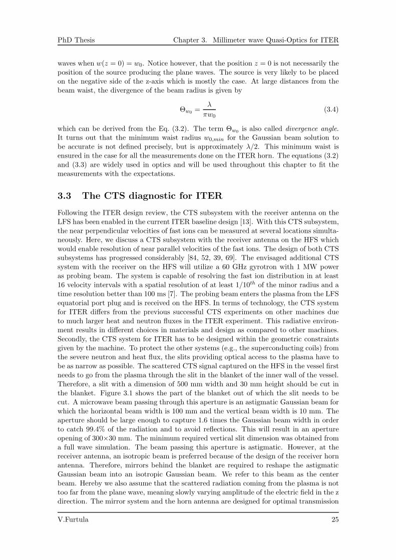
Following the ITER design review, the CTS subsystem with the receiver antenna on theLFS has been enabled in the current ITER baseline design [13]. With this CTS subsystem,the near perpendicular velocities of fast ions can be measured at several locations simulta-neously. Here, we discuss a CTS subsystem with the receiver antenna on the HFS whichwould enable resolution of near parallel velocities of the fast ions. The design of both CTSsubsystems has progressed considerably [84, 52, 39, 69]. The envisaged additional CTSsystem with the receiver on the HFS will utilize a 60 GHz gyrotron with 1 MW poweras probing beam. The system is capable of resolving the fast ion distribution in at least16 velocity intervals with a spatial resolution of at least 1/10th of the minor radius and atime resolution better than 100 ms [7]. The probing beam enters the plasma from the LFSequatorial port plug and is received on the HFS. In terms of technology, the CTS systemfor ITER differs from the previous successful CTS experiments on other machines dueto much larger heat and neutron fluxes in the ITER experiment. This radiative environ-ment results in different choices in materials and design as compared to other machines.Secondly, the CTS system for ITER has to be designed within the geometric constraintsgiven by the machine. To protect the other systems (e.g., the superconducting coils) fromthe severe neutron and heat flux, the slits providing optical access to the plasma have tobe as narrow as possible. The scattered CTS signal captured on the HFS in the vessel firstneeds to go from the plasma through the slit in the blanket of the inner wall of the vessel.Therefore, a slit with a dimension of 500 mm width and 30 mm height should be cut inthe blanket. Figure 3.1 shows the part of the blanket out of which the slit needs to becut. A microwave beam passing through this aperture is an astigmatic Gaussian beam forwhich the horizontal beam width is 100 mm and the vertical beam width is 10 mm. Theaperture should be large enough to capture 1.6 times the Gaussian beam width in orderto catch 99.4% of the radiation and to avoid reflections. This will result in an apertureopening of 300×30 mm. The minimum required vertical slit dimension was obtained froma full wave simulation. The beam passing this aperture is astigmatic. However, at thereceiver antenna, an isotropic beam is preferred because of the design of the receiver hornantenna. Therefore, mirrors behind the blanket are required to reshape the astigmaticGaussian beam into an isotropic Gaussian beam. We refer to this beam as the centerbeam. Hereby we also assume that the scattered radiation coming from the plasma is nottoo far from the plane wave, meaning slowly varying amplitude of the electric field in the zdirection. The mirror system and the horn antenna are designed for optimal transmission
V.Furtula 25
PhD Thesis Chapter 3. Millimeter wave Quasi-Optics for ITER
Figure 3.1: The additional envisaged CTS system on ITER with an antenna on the HFS wouldrequire a slit (green, 500 × 30 mm) in the blanket of the inner wall. The figure isreproduced with permission [46].
of the center beam. Since the fast ion distribution shall be measured at several loca-tions in the plasma, beams from different incident angles (±15) in the horizontal planeshall be accepted. This requires the enlarged aperture in the horizontal direction witha width of approximately 500 mm. Beams coming from different angles with respect tothe center beam require different horn positions since the mirrors are fixed. The distancebetween these horn antennas determine the distance between measurement locations inthe plasma. In this work, only the center beam is considered.
3.4 Design of the HFS antenna
The space for the mirrors behind the blanket is limited to 190 mm vertically, 300 mmhorizontally, and 230 mm radially. The beam parameters at the slit in the blanket aregiven by the slit dimensions. The mirror shapes for a quasioptical transmission line wereassumed to be a surface of a torus, while the major and minor radii of the torus couldbe varied in the computations. The reflection of an incoming beam on a surface (in ourcase the torus surface) was calculated and fitted to an astigmatic Gaussian beam. Severaliterations where required to find a good solution. The computing code is based on Matlablanguage and has been written in-house by Henrik Bindslev.
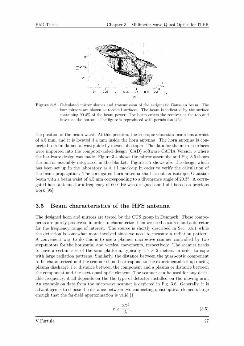
The distance between two adjacent measurement locations in the plasma is determinedby the distance between two adjacent horn antennas and therefore limited by the beamsize. A small beam size allows a close arrangement of the horn antennas and thereforeallows decreasing the distance between measurement locations in the plasma. In order toreshape an astigmatic beam with given widths and curvatures at the beginning and atthe end of the beam, at least two mirrors are required. Due to the large difference in thebeam dimensions between slit and horn antenna, the reshaping should be performed on apropagation path long enough to be well within the paraxial approximation of Gaussianbeam propagation. Due to the limited space, a long, straight path is not possible. There-fore, two additional mirrors were employed to increase the optical path length betweenthe slit and the horn antenna. The mirror shapes, which are required to reshape the beamaccording to these boundary conditions, are calculated. Mathematically, the mirrors aresurfaces of tori. The mirror surfaces and the beam shape are shown in Fig. 3.2. Thebeam enters the receiver at the top and leaves at the bottom. Figure 3.3 shows the beamwidth for the two major axes along the path of propagation through the quasi-opticaltransmission line. The triangles indicate positions of the mirrors, the diamond indicates
V.Furtula 26
PhD Thesis Chapter 3. Millimeter wave Quasi-Optics for ITER
Figure 3.2: Calculated mirror shapes and transmission of the astigmatic Gaussian beam. Thefour mirrors are shown as toroidal surfaces. The beam is indicated by the surfacecontaining 99.4% of the beam power. The beam enters the receiver at the top andleaves at the bottom. The figure is reproduced with permission [46].
the position of the beam waist. At this position, the isotropic Gaussian beam has a waistof 4.5 mm, and it is located 3.4 mm inside the horn antenna. The horn antenna is con-nected to a fundamental waveguide by means of a taper. The data for the mirror surfaceswere imported into the computer-aided design (CAD) software CATIA Version 5 wherethe hardware design was made. Figure 3.4 shows the mirror assembly, and Fig. 3.5 showsthe mirror assembly integrated in the blanket. Figure 3.5 shows also the design whichhas been set up in the laboratory as a 1:1 mock-up in order to verify the calculation ofthe beam propagation. The corrugated horn antenna shall accept an isotropic Gaussianbeam with a beam waist of 4.5 mm corresponding to a divergence angle of 20.3. A corru-gated horn antenna for a frequency of 60 GHz was designed and built based on previouswork [95].
3.5 Beam characteristics of the HFS antenna
The designed horn and mirrors are tested by the CTS group in Denmark. These compo-nents are purely passive so in order to characterize them we need a source and a detectorfor the frequency range of interest. The source is shortly described in Sec. 3.5.1 whilethe detection is somewhat more involved since we need to measure a radiation pattern.A convenient way to do this is to use a planner microwave scanner controlled by twostep-motors for the horizontal and vertical movements, respectively. The scanner needsto have a certain size of the scan platform, typically 1.5 × 2 meters, in order to copewith large radiation patterns. Similarly, the distance between the quasi-optic componentto be characterized and the scanner should correspond to the experimental set up duringplasma discharge, i.e. distance between the component and a plasma or distance betweenthe component and the next quasi-optic element. The scanner can be used for any desir-able frequency, it all depends on the the type of detector installed on the moving arm.An example on data from the microwave scanner is depicted in Fig. 3.6. Generally, it isadvantageous to choose the distance between two connecting quasi-optical elements largeenough that the far-field approximation is valid [1]
r ≥ 2D2
λ, (3.5)
V.Furtula 27

PhD Thesis Chapter 3. Millimeter wave Quasi-Optics for ITER
0 0.1 0.2 0.3 0.4 0.50
0.02
0.04
0.06
0.08
0.1
0.12
Distance from blanket to receiver [m]
Gau
ssia
n be
am w
idth
[m]
M1 M2 M3 M4
Y−Direction
Z−Direction
Figure 3.3: Gaussian beam widths in the two orthogonal directions in the transmission lines.Between the reference point and mirror M1, the two orthogonal directions coincidewith the y-axis (blue curve) and the z-axis (red curve). The triangles indicate themirror positions M1 to M4 and the diamond indicates the position of the waistwhich is located slightly inside the horn antenna. See also Fig. 3.8. The figure isreproduced with permission [46].
M1 M3
M2
M4
Figure 3.4: Mirror assembly (Mirrors M1-M4) for the HFS CTS transmission line. The redsurfaces are the mirror surfaces calculated and imported into CATIA. The yellowsurface represents 1.6 times the Gaussian beam width of the astigmatic Gaussianbeam. See also Fig. 3.8.
V.Furtula 28
PhD Thesis Chapter 3. Millimeter wave Quasi-Optics for ITER
M1
M3
Mirror Assembly
Blanket
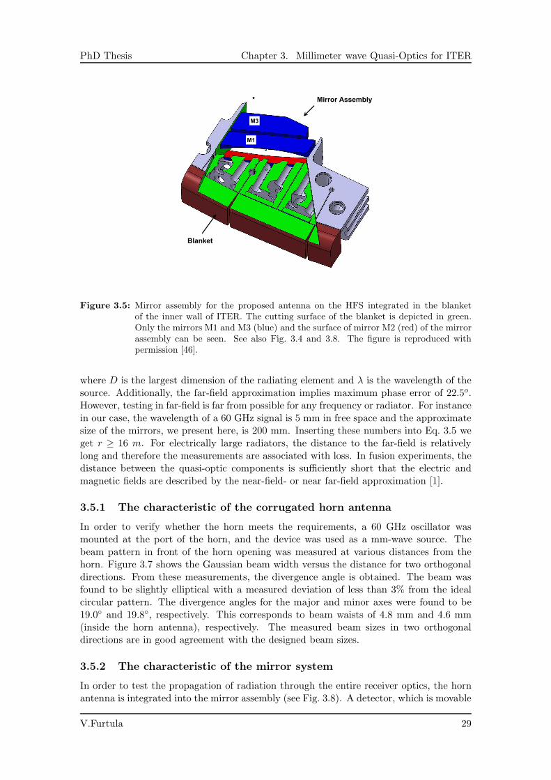
Figure 3.5: Mirror assembly for the proposed antenna on the HFS integrated in the blanketof the inner wall of ITER. The cutting surface of the blanket is depicted in green.Only the mirrors M1 and M3 (blue) and the surface of mirror M2 (red) of the mirrorassembly can be seen. See also Fig. 3.4 and 3.8. The figure is reproduced withpermission [46].
where D is the largest dimension of the radiating element and λ is the wavelength of thesource. Additionally, the far-field approximation implies maximum phase error of 22.5o.However, testing in far-field is far from possible for any frequency or radiator. For instancein our case, the wavelength of a 60 GHz signal is 5 mm in free space and the approximatesize of the mirrors, we present here, is 200 mm. Inserting these numbers into Eq. 3.5 weget r ≥ 16 m. For electrically large radiators, the distance to the far-field is relativelylong and therefore the measurements are associated with loss. In fusion experiments, thedistance between the quasi-optic components is sufficiently short that the electric andmagnetic fields are described by the near-field- or near far-field approximation [1].
3.5.1 The characteristic of the corrugated horn antenna
In order to verify whether the horn meets the requirements, a 60 GHz oscillator wasmounted at the port of the horn, and the device was used as a mm-wave source. Thebeam pattern in front of the horn opening was measured at various distances from thehorn. Figure 3.7 shows the Gaussian beam width versus the distance for two orthogonaldirections. From these measurements, the divergence angle is obtained. The beam wasfound to be slightly elliptical with a measured deviation of less than 3% from the idealcircular pattern. The divergence angles for the major and minor axes were found to be19.0 and 19.8, respectively. This corresponds to beam waists of 4.8 mm and 4.6 mm(inside the horn antenna), respectively. The measured beam sizes in two orthogonaldirections are in good agreement with the designed beam sizes.
3.5.2 The characteristic of the mirror system
In order to test the propagation of radiation through the entire receiver optics, the hornantenna is integrated into the mirror assembly (see Fig. 3.8). A detector, which is movable
V.Furtula 29
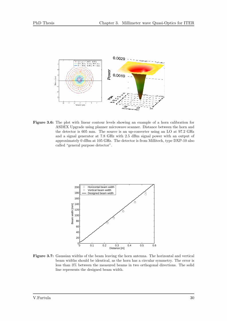
PhD Thesis Chapter 3. Millimeter wave Quasi-Optics for ITER
Figure 3.6: The plot with linear contour levels showing an example of a horn calibration forASDEX Upgrade using planner microwave scanner. Distance between the horn andthe detector is 605 mm. The source is an up-converter using an LO at 97.2 GHzand a signal generator at 7.8 GHz with 2.5 dBm signal power with an output ofapproximately 0 dBm at 105 GHz. The detector is from Millitech, type DXP-10 alsocalled “general purpose detector”.
0 0.1 0.2 0.3 0.4 0.5 0.60
20
40
60
80
100
120
140
160
180
200
Distance [m]
Bea
m w
idth
[mm
]
Horizontal beam widthVertical beam widthDesigned beam width
Figure 3.7: Gaussian widths of the beam leaving the horn antenna. The horizontal and verticalbeam widths should be identical, as the horn has a circular symmetry. The error isless than 3% between the measured beams in two orthogonal directions. The solidline represents the designed beam width.
V.Furtula 30
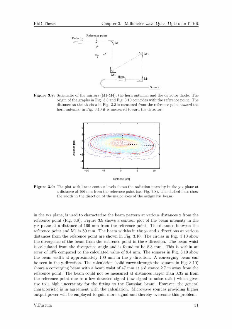
PhD Thesis Chapter 3. Millimeter wave Quasi-Optics for ITER
Figure 3.8: Schematic of the mirrors (M1-M4), the horn antenna, and the detector diode. Theorigin of the graphs in Fig. 3.3 and Fig. 3.10 coincides with the reference point. Thedistance on the abscissa in Fig. 3.3 is measured from the reference point toward thehorn antenna; in Fig. 3.10 it is measured toward the detector.
−10 −5 0 5 10−6
−4
−2
0
2
4
6
Distance [cm]
Dis
tanc
e [c
m]
Figure 3.9: The plot with linear contour levels shows the radiation intensity in the y-z-plane ata distance of 166 mm from the reference point (see Fig. 3.8). The dashed lines showthe width in the direction of the major axes of the astigmatic beam.
in the y-z plane, is used to characterize the beam pattern at various distances x from thereference point (Fig. 3.8). Figure 3.9 shows a contour plot of the beam intensity in they-z plane at a distance of 166 mm from the reference point. The distance between thereference point and M1 is 80 mm. The beam widths in the y- and z directions at variousdistances from the reference point are shown in Fig. 3.10. The circles in Fig. 3.10 showthe divergence of the beam from the reference point in the z-direction. The beam waistis calculated from the divergence angle and is found to be 8.3 mm. This is within anerror of 13% compared to the calculated value of 9.4 mm. The squares in Fig. 3.10 showthe beam width at approximately 100 mm in the y direction. A converging beam canbe seen in the y-direction. The calculation (solid curve through the squares in Fig. 3.10)shows a converging beam with a beam waist of 47 mm at a distance 2.7 m away from thereference point. The beam could not be measured at distances larger than 0.35 m fromthe reference point due to a low detected signal (low signal-to-noise ratio) which givesrise to a high uncertainty for the fitting to the Gaussian beam. However, the generalcharacteristic is in agreement with the calculation. Microwave sources providing higheroutput power will be employed to gain more signal and thereby overcome this problem.
V.Furtula 31
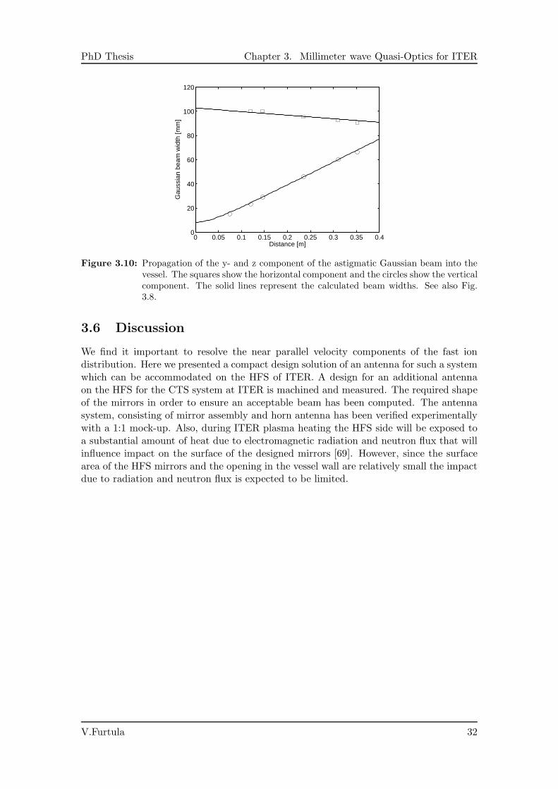
PhD Thesis Chapter 3. Millimeter wave Quasi-Optics for ITER
0 0.05 0.1 0.15 0.2 0.25 0.3 0.35 0.40
20
40
60
80
100
120
Distance [m]
Gau
ssia
n be
am w
idth
[mm
]
Figure 3.10: Propagation of the y- and z component of the astigmatic Gaussian beam into thevessel. The squares show the horizontal component and the circles show the verticalcomponent. The solid lines represent the calculated beam widths. See also Fig.3.8.
3.6 Discussion
We find it important to resolve the near parallel velocity components of the fast iondistribution. Here we presented a compact design solution of an antenna for such a systemwhich can be accommodated on the HFS of ITER. A design for an additional antennaon the HFS for the CTS system at ITER is machined and measured. The required shapeof the mirrors in order to ensure an acceptable beam has been computed. The antennasystem, consisting of mirror assembly and horn antenna has been verified experimentallywith a 1:1 mock-up. Also, during ITER plasma heating the HFS side will be exposed toa substantial amount of heat due to electromagnetic radiation and neutron flux that willinfluence impact on the surface of the designed mirrors [69]. However, since the surfacearea of the HFS mirrors and the opening in the vessel wall are relatively small the impactdue to radiation and neutron flux is expected to be limited.
V.Furtula 32
Chapter 4
CTS Receiver at ASDEX Upgrade
4.1 Short background and introduction
The principles behind CTS receiver installed at ASDEX Upgrade are presented in thischapter. The receiver can detect spectral power densities of a few eV against the ECEbackground on the order of 100 eV under presence of gyrotron stray radiation that isseveral orders of magnitude stronger than the signal to be detected. We present measure-ments of the transmission characteristics and performance of the main receiver compo-nents operating at mm-wave frequencies (notch-, bandpass- and lowpass filters, a voltage-controlled variable attenuator, and an isolator), the down-converter unit, and the inter-mediate frequency (IF) components (amplifiers, bandpass filters, and detector diodes).Furthermore, we determine the performance of the receiver as a unit through spectralresponse measurements and find reasonable agreement with the expectation based on theindividual component measurements.
Radiometers are remote sensing instruments that collect electromagnetic radiationin the millimeter and submillimeter wavelength range (30 GHz-3 THz) and measure itsspectral power density. The CTS receiver we discuss here is a radiometer designed todetect radiation in the frequency range 100-110 GHz with a heterodyne detection scheme.This is the expected Doppler-shift frequency range for gyrotron 105 GHz radiation scat-tered due to presence of fast ions with energies up to 500 keV in the plasma at ASDEXUpgrade (AUG). Seen from a broader perspective, there exist three types of radiometerthat are suitable for usage as microwave receivers in hot plasma diagnostics. The firsttype is the total power radiometer (TPR [83, 75]) which is the type that we use to detectthe scattered signals from fusion plasmas. A TPR is characterized by simple detection ofthe electromagnetic radiation seen by the quasioptical mirrors and horn. The radiationis then divided in several channels by a heterodyne method, and then the average powerin each channel is converted linearly to a voltage using square law diodes. The secondtype is the Dicke radiometer (DR [75]) which is used not to measure directly the antennatemperature as in TPR, but rather difference between this and some known referencetemperature. The sensitivity of the measurement to gain and noise temperature insta-bilities is greatly reduced. The third type is the noise-injection radiometer (NIR) whichrepresents a step towards best achievable accuracy, meaning the output is independent ofgain and noise temperature fluctuations. NIR is a specialized type of DR where the con-dition of equal reference temperature and antenna temperature is continuously ensuredby a servo loop. Overviews of heterodyne methods used for plasma diagnostics are given
33
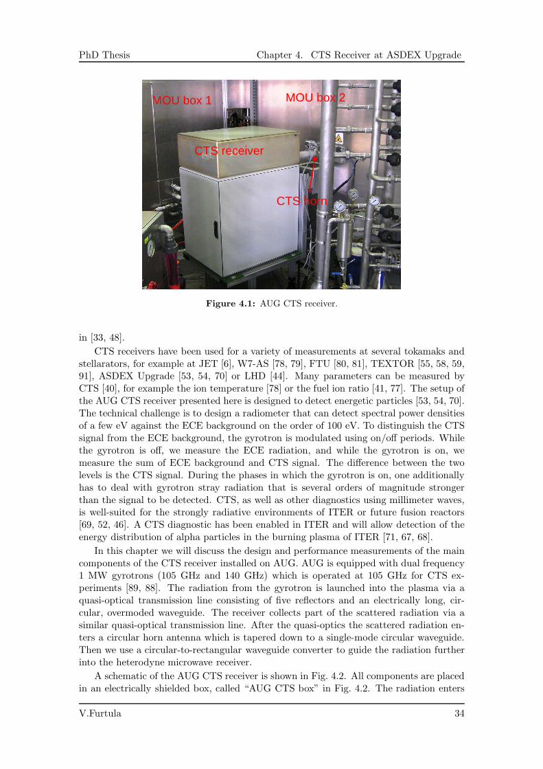
PhD Thesis Chapter 4. CTS Receiver at ASDEX Upgrade
CTS receiver
CTS horn
MOU box 1 MOU box 2
Figure 4.1: AUG CTS receiver.
in [33, 48].
CTS receivers have been used for a variety of measurements at several tokamaks andstellarators, for example at JET [6], W7-AS [78, 79], FTU [80, 81], TEXTOR [55, 58, 59,91], ASDEX Upgrade [53, 54, 70] or LHD [44]. Many parameters can be measured byCTS [40], for example the ion temperature [78] or the fuel ion ratio [41, 77]. The setup ofthe AUG CTS receiver presented here is designed to detect energetic particles [53, 54, 70].The technical challenge is to design a radiometer that can detect spectral power densitiesof a few eV against the ECE background on the order of 100 eV. To distinguish the CTSsignal from the ECE background, the gyrotron is modulated using on/off periods. Whilethe gyrotron is off, we measure the ECE radiation, and while the gyrotron is on, wemeasure the sum of ECE background and CTS signal. The difference between the twolevels is the CTS signal. During the phases in which the gyrotron is on, one additionallyhas to deal with gyrotron stray radiation that is several orders of magnitude strongerthan the signal to be detected. CTS, as well as other diagnostics using millimeter waves,is well-suited for the strongly radiative environments of ITER or future fusion reactors[69, 52, 46]. A CTS diagnostic has been enabled in ITER and will allow detection of theenergy distribution of alpha particles in the burning plasma of ITER [71, 67, 68].
In this chapter we will discuss the design and performance measurements of the maincomponents of the CTS receiver installed on AUG. AUG is equipped with dual frequency1 MW gyrotrons (105 GHz and 140 GHz) which is operated at 105 GHz for CTS ex-periments [89, 88]. The radiation from the gyrotron is launched into the plasma via aquasi-optical transmission line consisting of five reflectors and an electrically long, cir-cular, overmoded waveguide. The receiver collects part of the scattered radiation via asimilar quasi-optical transmission line. After the quasi-optics the scattered radiation en-ters a circular horn antenna which is tapered down to a single-mode circular waveguide.Then we use a circular-to-rectangular waveguide converter to guide the radiation furtherinto the heterodyne microwave receiver.
A schematic of the AUG CTS receiver is shown in Fig. 4.2. All components are placedin an electrically shielded box, called “AUG CTS box” in Fig. 4.2. The radiation enters
V.Furtula 34
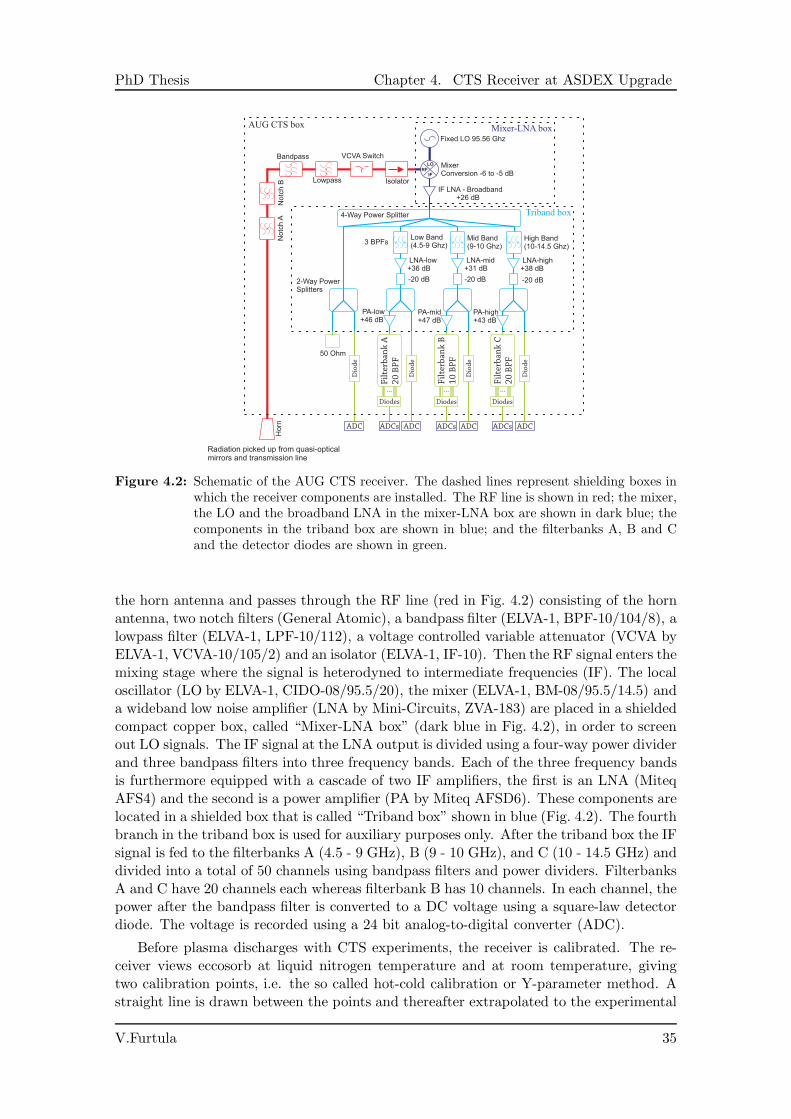
PhD Thesis Chapter 4. CTS Receiver at ASDEX Upgrade
Figure 4.2: Schematic of the AUG CTS receiver. The dashed lines represent shielding boxes inwhich the receiver components are installed. The RF line is shown in red; the mixer,the LO and the broadband LNA in the mixer-LNA box are shown in dark blue; thecomponents in the triband box are shown in blue; and the filterbanks A, B and Cand the detector diodes are shown in green.
the horn antenna and passes through the RF line (red in Fig. 4.2) consisting of the hornantenna, two notch filters (General Atomic), a bandpass filter (ELVA-1, BPF-10/104/8), alowpass filter (ELVA-1, LPF-10/112), a voltage controlled variable attenuator (VCVA byELVA-1, VCVA-10/105/2) and an isolator (ELVA-1, IF-10). Then the RF signal enters themixing stage where the signal is heterodyned to intermediate frequencies (IF). The localoscillator (LO by ELVA-1, CIDO-08/95.5/20), the mixer (ELVA-1, BM-08/95.5/14.5) anda wideband low noise amplifier (LNA by Mini-Circuits, ZVA-183) are placed in a shieldedcompact copper box, called “Mixer-LNA box” (dark blue in Fig. 4.2), in order to screenout LO signals. The IF signal at the LNA output is divided using a four-way power dividerand three bandpass filters into three frequency bands. Each of the three frequency bandsis furthermore equipped with a cascade of two IF amplifiers, the first is an LNA (MiteqAFS4) and the second is a power amplifier (PA by Miteq AFSD6). These components arelocated in a shielded box that is called “Triband box” shown in blue (Fig. 4.2). The fourthbranch in the triband box is used for auxiliary purposes only. After the triband box the IFsignal is fed to the filterbanks A (4.5 - 9 GHz), B (9 - 10 GHz), and C (10 - 14.5 GHz) anddivided into a total of 50 channels using bandpass filters and power dividers. FilterbanksA and C have 20 channels each whereas filterbank B has 10 channels. In each channel, thepower after the bandpass filter is converted to a DC voltage using a square-law detectordiode. The voltage is recorded using a 24 bit analog-to-digital converter (ADC).
Before plasma discharges with CTS experiments, the receiver is calibrated. The re-ceiver views eccosorb at liquid nitrogen temperature and at room temperature, givingtwo calibration points, i.e. the so called hot-cold calibration or Y-parameter method. Astraight line is drawn between the points and thereafter extrapolated to the experimental
V.Furtula 35
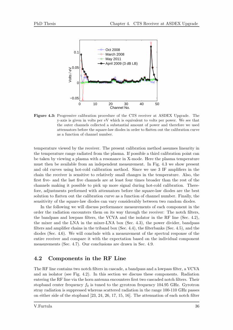
PhD Thesis Chapter 4. CTS Receiver at ASDEX Upgrade
0 10 20 30 40 50
−0.05
0
0.05
0.1
Vol
ts /
eV
Channel No.
Oct 2008March 2008May 2011April 2009 (3 dB LB)
Figure 4.3: Progressive calibration procedure of the CTS receiver at ASDEX Upgrade. They-axis is given in volts per eV which is equivalent to volts per power. We see thatthe outer channels collected a substantial amount of power and therefore we usedattenuators before the square-law diodes in order to flatten out the calibration curveas a function of channel number.
temperature viewed by the receiver. The present calibration method assumes linearity inthe temperature range radiated from the plasma. If possible a third calibration point canbe taken by viewing a plasma with a resonance in X-mode. Here the plasma temperaturemust then be available from an independent measurement. In Fig. 4.3 we show presentand old curves using hot-cold calibration method. Since we use 3 IF amplifiers in thechain the receiver is sensitive to relatively small changes in the temperature. Also, thefirst five- and the last five channels are at least four times broader than the rest of thechannels making it possible to pick up more signal during hot-cold calibration. There-fore, adjustments performed with attenuators before the square-law diodes are the bestsolution to flatten out the calibration curve as a function of channel number. Finally, thesensitivity of the square-law diodes can vary considerably between two random diodes.
In the following we will discuss performance measurements of each component in theorder the radiation encounters them on its way through the receiver: The notch filters,the bandpass and lowpass filters, the VCVA and the isolator in the RF line (Sec. 4.2),the mixer and the LNA in the mixer-LNA box (Sec. 4.3), the power divider, bandpassfilters and amplifier chains in the triband box (Sec. 4.4), the filterbanks (Sec. 4.5), and thediodes (Sec. 4.6). We will conclude with a measurement of the spectral response of theentire receiver and compare it with the expectation based on the individual componentmeasurements (Sec. 4.7). Our conclusions are drawn in Sec. 4.9.
4.2 Components in the RF Line
The RF line contains two notch filters in cascade, a bandpass and a lowpass filter, a VCVAand an isolator (see Fig. 4.2). In this section we discuss these components. Radiationentering the RF line via the horn antenna encounters first two cascaded notch filters. Theirstopband center frequency f0 is tuned to the gyrotron frequency 104.95 GHz. Gyrotronstray radiation is suppressed whereas scattered radiation in the range 100-110 GHz passeson either side of the stopband [23, 24, 26, 17, 15, 16]. The attenuation of each notch filter
V.Furtula 36
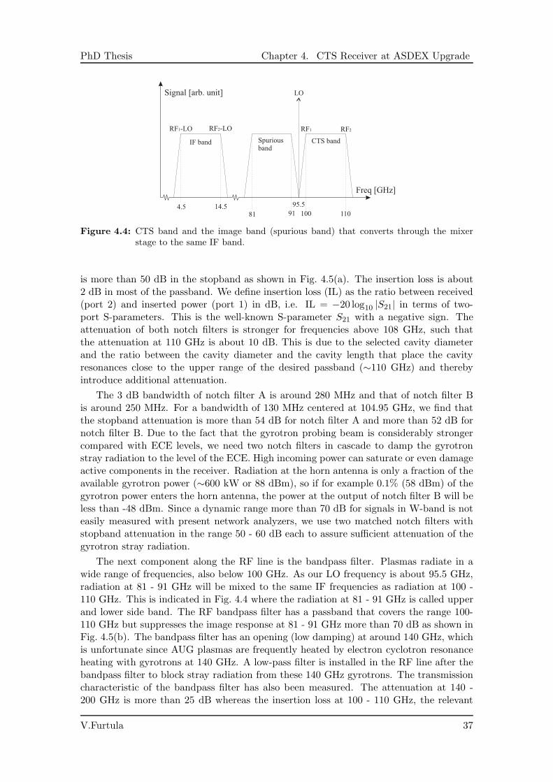
PhD Thesis Chapter 4. CTS Receiver at ASDEX Upgrade
Figure 4.4: CTS band and the image band (spurious band) that converts through the mixerstage to the same IF band.
is more than 50 dB in the stopband as shown in Fig. 4.5(a). The insertion loss is about2 dB in most of the passband. We define insertion loss (IL) as the ratio between received(port 2) and inserted power (port 1) in dB, i.e. IL = −20 log10 |S21| in terms of two-port S-parameters. This is the well-known S-parameter S21 with a negative sign. Theattenuation of both notch filters is stronger for frequencies above 108 GHz, such thatthe attenuation at 110 GHz is about 10 dB. This is due to the selected cavity diameterand the ratio between the cavity diameter and the cavity length that place the cavityresonances close to the upper range of the desired passband (∼110 GHz) and therebyintroduce additional attenuation.
The 3 dB bandwidth of notch filter A is around 280 MHz and that of notch filter Bis around 250 MHz. For a bandwidth of 130 MHz centered at 104.95 GHz, we find thatthe stopband attenuation is more than 54 dB for notch filter A and more than 52 dB fornotch filter B. Due to the fact that the gyrotron probing beam is considerably strongercompared with ECE levels, we need two notch filters in cascade to damp the gyrotronstray radiation to the level of the ECE. High incoming power can saturate or even damageactive components in the receiver. Radiation at the horn antenna is only a fraction of theavailable gyrotron power (∼600 kW or 88 dBm), so if for example 0.1% (58 dBm) of thegyrotron power enters the horn antenna, the power at the output of notch filter B will beless than -48 dBm. Since a dynamic range more than 70 dB for signals in W-band is noteasily measured with present network analyzers, we use two matched notch filters withstopband attenuation in the range 50 - 60 dB each to assure sufficient attenuation of thegyrotron stray radiation.
The next component along the RF line is the bandpass filter. Plasmas radiate in awide range of frequencies, also below 100 GHz. As our LO frequency is about 95.5 GHz,radiation at 81 - 91 GHz will be mixed to the same IF frequencies as radiation at 100 -110 GHz. This is indicated in Fig. 4.4 where the radiation at 81 - 91 GHz is called upperand lower side band. The RF bandpass filter has a passband that covers the range 100-110 GHz but suppresses the image response at 81 - 91 GHz more than 70 dB as shown inFig. 4.5(b). The bandpass filter has an opening (low damping) at around 140 GHz, whichis unfortunate since AUG plasmas are frequently heated by electron cyclotron resonanceheating with gyrotrons at 140 GHz. A low-pass filter is installed in the RF line after thebandpass filter to block stray radiation from these 140 GHz gyrotrons. The transmissioncharacteristic of the bandpass filter has also been measured. The attenuation at 140 -200 GHz is more than 25 dB whereas the insertion loss at 100 - 110 GHz, the relevant
V.Furtula 37
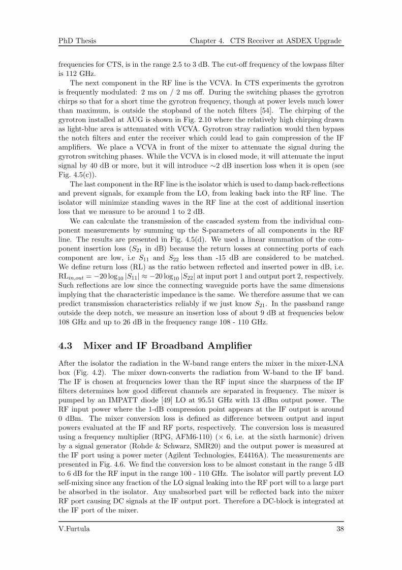
PhD Thesis Chapter 4. CTS Receiver at ASDEX Upgrade
frequencies for CTS, is in the range 2.5 to 3 dB. The cut-off frequency of the lowpass filteris 112 GHz.
The next component in the RF line is the VCVA. In CTS experiments the gyrotronis frequently modulated: 2 ms on / 2 ms off. During the switching phases the gyrotronchirps so that for a short time the gyrotron frequency, though at power levels much lowerthan maximum, is outside the stopband of the notch filters [54]. The chirping of thegyrotron installed at AUG is shown in Fig. 2.10 where the relatively high chirping drawnas light-blue area is attenuated with VCVA. Gyrotron stray radiation would then bypassthe notch filters and enter the receiver which could lead to gain compression of the IFamplifiers. We place a VCVA in front of the mixer to attenuate the signal during thegyrotron switching phases. While the VCVA is in closed mode, it will attenuate the inputsignal by 40 dB or more, but it will introduce ∼2 dB insertion loss when it is open (seeFig. 4.5(c)).
The last component in the RF line is the isolator which is used to damp back-reflectionsand prevent signals, for example from the LO, from leaking back into the RF line. Theisolator will minimize standing waves in the RF line at the cost of additional insertionloss that we measure to be around 1 to 2 dB.
We can calculate the transmission of the cascaded system from the individual com-ponent measurements by summing up the S-parameters of all components in the RFline. The results are presented in Fig. 4.5(d). We used a linear summation of the com-ponent insertion loss (S21 in dB) because the return losses at connecting ports of eachcomponent are low, i.e S11 and S22 less than -15 dB are considered to be matched.We define return loss (RL) as the ratio between reflected and inserted power in dB, i.e.RLin,out = −20 log10 |S11| ≈ −20 log10 |S22| at input port 1 and output port 2, respectively.Such reflections are low since the connecting waveguide ports have the same dimensionsimplying that the characteristic impedance is the same. We therefore assume that we canpredict transmission characteristics reliably if we just know S21. In the passband rangeoutside the deep notch, we measure an insertion loss of about 9 dB at frequencies below108 GHz and up to 26 dB in the frequency range 108 - 110 GHz.
4.3 Mixer and IF Broadband Amplifier
After the isolator the radiation in the W-band range enters the mixer in the mixer-LNAbox (Fig. 4.2). The mixer down-converts the radiation from W-band to the IF band.The IF is chosen at frequencies lower than the RF input since the sharpness of the IFfilters determines how good different channels are separated in frequency. The mixer ispumped by an IMPATT diode [49] LO at 95.51 GHz with 13 dBm output power. TheRF input power where the 1-dB compression point appears at the IF output is around0 dBm. The mixer conversion loss is defined as difference between output and inputpowers evaluated at the IF and RF ports, respectively. The conversion loss is measuredusing a frequency multiplier (RPG, AFM6-110) (× 6, i.e. at the sixth harmonic) drivenby a signal generator (Rohde & Schwarz, SMR20) and the output power is measured atthe IF port using a power meter (Agilent Technologies, E4416A). The measurements arepresented in Fig. 4.6. We find the conversion loss to be almost constant in the range 5 dBto 6 dB for the RF input in the range 100 - 110 GHz. The isolator will partly prevent LOself-mixing since any fraction of the LO signal leaking into the RF port will to a large partbe absorbed in the isolator. Any unabsorbed part will be reflected back into the mixerRF port causing DC signals at the IF output port. Therefore a DC-block is integrated atthe IF port of the mixer.
V.Furtula 38
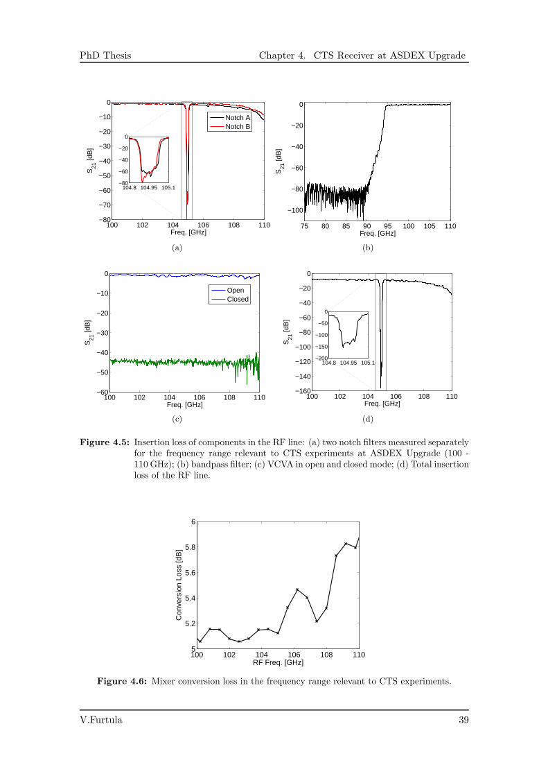
PhD Thesis Chapter 4. CTS Receiver at ASDEX Upgrade
100 102 104 106 108 110−80
−70
−60
−50
−40
−30
−20
−10
0
S21
[dB
]
Freq. [GHz]
Notch ANotch B
104.8 104.95 105.1−80
−60
−40
−20
0
(a)
75 80 85 90 95 100 105 110
−100
−80
−60
−40
−20
0
S21
[dB
]
Freq. [GHz]
(b)
100 102 104 106 108 110−60
−50
−40
−30
−20
−10
0
Freq. [GHz]
S21
[dB
]
OpenClosed
(c)
100 102 104 106 108 110−160
−140
−120
−100
−80
−60
−40
−20
0
S21
[dB
]
Freq. [GHz]
104.8 104.95 105.1−200
−150
−100
−50
0
(d)
Figure 4.5: Insertion loss of components in the RF line: (a) two notch filters measured separatelyfor the frequency range relevant to CTS experiments at ASDEX Upgrade (100 -110 GHz); (b) bandpass filter; (c) VCVA in open and closed mode; (d) Total insertionloss of the RF line.
100 102 104 106 108 1105
5.2
5.4
5.6
5.8
6
Con
vers
ion
Loss
[dB
]
RF Freq. [GHz]
Figure 4.6: Mixer conversion loss in the frequency range relevant to CTS experiments.
V.Furtula 39
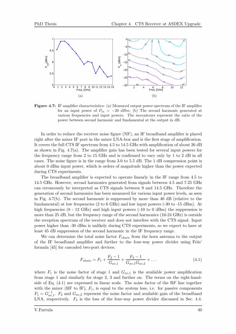
PhD Thesis Chapter 4. CTS Receiver at ASDEX Upgrade
0 1 2 3 4 5 6 7 8 9 10 11 12 13 14 155
5.5
6
6.5
7
Pou
t[dB
m]
Freq. [GHz]
(a)
20 20
25
25
25
30
30
30
30
30
35
35
35
35
40
40
40
40
45
45
45
45
50
50
55
Pin
[dB
m]
Freq. [GHz]2 4 6 8 10 12
−30
−25
−20
−15
−10
−5
0
(b)
Figure 4.7: IF amplifier characteristics: (a) Measured output power spectrum of the IF amplifierfor an input power of Pin = −20 dBm; (b) The second harmonic generated atvarious frequencies and input powers. The isocontours represent the ratio of thepower between second harmonic and fundamental at the output in dB.
In order to reduce the receiver noise figure (NF), an IF broadband amplifier is placedright after the mixer IF port in the mixer LNA-box and is the first stage of amplification.It covers the full CTS IF spectrum from 4.5 to 14.5 GHz with amplification of about 26 dBas shown in Fig. 4.7(a). The amplifier gain has been tested for several input powers forthe frequency range from 2 to 15 GHz and is confirmed to vary only by 1 to 2 dB in allcases. The noise figure is in the range from 3.0 to 5.5 dB. The 1 dB compression point isabout 0 dBm input power, which is orders of magnitude higher than the power expectedduring CTS experiments.
The broadband amplifier is expected to operate linearly in the IF range from 4.5 to14.5 GHz. However, second harmonics generated from signals between 4.5 and 7.25 GHzcan erroneously be interpreted as CTS signals between 9 and 14.5 GHz. Therefore thegeneration of second harmonics has been measured for various input power levels, as seenin Fig. 4.7(b). The second harmonic is suppressed by more than 40 dB (relative to thefundamental) at low frequencies (2 to 6 GHz) and low input powers (-30 to -15 dBm). Athigh frequencies (8 - 12 GHz) and high input powers (-10 to 0 dBm) the suppression ismore than 25 dB, but the frequency range of the second harmonics (16-24 GHz) is outsidethe reception spectrum of the receiver and does not interfere with the CTS signal. Inputpower higher than -30 dBm is unlikely during CTS experiments, so we expect to have atleast 45 dB suppression of the second harmonic in the IF frequency range.
We can determine the total noise factor Fchain from the horn antenna to the outputof the IF broadband amplifier and further to the four-way power divider using Friis’formula [45] for cascaded two-port devices.
Fchain = F1 +F2 − 1
Gav,1+
F3 − 1
Gav,1Gav,2+ . . . (4.1)
where F1 is the noise factor of stage 1 and Gav,1 is the available power amplificationfrom stage 1 and similarly for stage 2, 3 and further on. The terms on the right-hand-side of Eq. (4.1) are expressed in linear scale. The noise factor of the RF line togetherwith the mixer (RF to IF), F1, is equal to the system loss, i.e. for passive componentsF1 = G−1
av,1. F2 and Gav,2 represent the noise factor and available gain of the broadbandLNA, respectively. F3 is the loss of the four-way power divider discussed in Sec. 4.4.
V.Furtula 40
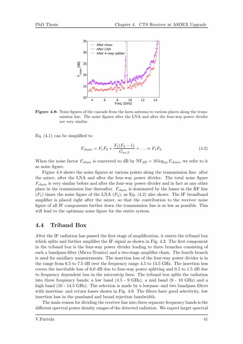
PhD Thesis Chapter 4. CTS Receiver at ASDEX Upgrade
4 6 8 10 12 1410
15
20
25
30
35
Freq. [GHz]
Fch
ain [d
B]
After mixerAfter LNAAfter 4−way splitter
Figure 4.8: Noise figures of the cascade from the horn antenna to various places along the trans-mission line. The noise figures after the LNA and after the four-way power dividerare very similar.
Eq. (4.1) can be simplified to
Fchain = F1F2 +F1(F3 − 1)
Gav,2+ . . . ≈ F1F2. (4.2)
When the noise factor Fchain is converted to dB by NFdB = 10 log10 Fchain, we refer to itas noise figure.
Figure 4.8 shows the noise figures at various points along the transmission line: afterthe mixer, after the LNA and after the four-way power divider. The total noise figureFchain is very similar before and after the four-way power divider and in fact at any otherplace in the transmission line thereafter. Fchain is dominated by the losses in the RF line(F1) times the noise figure of the LNA (F2), as Eq. (4.2) also shows. The IF broadbandamplifier is placed right after the mixer, so that the contribution to the receiver noisefigure of all IF components further down the transmission line is as low as possible. Thiswill lead to the optimum noise figure for the entire system.
4.4 Triband Box
After the IF radiation has passed the first stage of amplification, it enters the triband boxwhich splits and further amplifies the IF signal as shown in Fig. 4.2. The first componentin the triband box is the four-way power divider leading to three branches consisting ofeach a bandpass filter (Micro-Tronics) and a two-stage amplifier chain. The fourth branchis used for auxiliary measurements. The insertion loss of the four-way power divider is inthe range from 6.5 to 7.5 dB over the frequency range 4.5 to 14.5 GHz. The insertion losscovers the inevitable loss of 6.0 dB due to four-way power splitting and 0.5 to 1.5 dB dueto frequency dependent loss in the microstrip lines. The triband box splits the radiationinto three frequency bands; a low band (4.5 - 9 GHz), a mid band (9 - 10 GHz) and ahigh band (10 - 14.5 GHz). The selection is made by a lowpass- and two bandpass filterswith insertion- and return losses shown in Fig. 4.9. The filters have good selectivity, lowinsertion loss in the passband and broad rejection bandwidth.
The main reason for dividing the receiver line into three separate frequency bands is thedifferent spectral power density ranges of the detected radiation. We expect larger spectral
V.Furtula 41
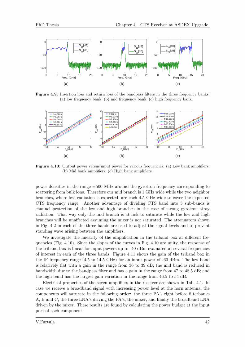
PhD Thesis Chapter 4. CTS Receiver at ASDEX Upgrade
0 5 10 15 20
−100
−50
0
Freq. [GHz]
S11
[dB]
S21
[dB]
(a)
0 5 10 15 20
−100
−50
0
Freq. [GHz]
S11
[dB]
S21
[dB]
(b)
0 5 10 15 20
−100
−50
0
Freq. [GHz]
S11
[dB]
S21
[dB]
(c)
Figure 4.9: Insertion loss and return loss of the bandpass filters in the three frequency banks:(a) low frequency bank; (b) mid frequency bank; (c) high frequency bank.
−60 −55 −50 −45 −40−20
−15
−10
−5
0
5
Pin
[dBm]
Pou
t[dB
m]
f=4.5GHzf=5.5GHzf=6.5GHzf=7.5GHzf=8.5GHz
(a)
−60 −55 −50 −45 −40−10
−5
0
5
10
15
Pin
[dBm]
Pou
t[dB
m]
f=9GHzf=9.2GHzf=9.4GHzf=9.6GHzf=9.8GHzf=10GHz
(b)
−60 −55 −50 −45 −40−10
−5
0
5
10
15
20
Pin
[dBm]P
out[d
Bm
]
f=10.0GHzf=10.8GHzf=11.6GHzf=12.4GHzf=13.2GHzf=14.0GHz
(c)
Figure 4.10: Output power versus input power for various frequencies: (a) Low bank amplifiers;(b) Mid bank amplifiers; (c) High bank amplifiers.
power densities in the range ±500 MHz around the gyrotron frequency corresponding toscattering from bulk ions. Therefore our mid branch is 1 GHz wide while the two neighborbranches, where less radiation is expected, are each 4.5 GHz wide to cover the expectedCTS frequency range. Another advantage of dividing CTS band into 3 sub-bands ischannel protection of the low and high branches in the case of strong gyrotron strayradiation. That way only the mid branch is at risk to saturate while the low and highbranches will be unaffected assuming the mixer is not saturated. The attenuators shownin Fig. 4.2 in each of the three bands are used to adjust the signal levels and to preventstanding wave arising between the amplifiers.
We investigate the linearity of the amplification in the triband box at different fre-quencies (Fig. 4.10). Since the slopes of the curves in Fig. 4.10 are unity, the response ofthe triband box is linear for input powers up to -40 dBm evaluated at several frequenciesof interest in each of the three bands. Figure 4.11 shows the gain of the triband box inthe IF frequency range (4.5 to 14.5 GHz) for an input power of -60 dBm. The low bandis relatively flat with a gain in the range from 36 to 39 dB; the mid band is reduced inbandwidth due to the bandpass filter and has a gain in the range from 47 to 48.5 dB; andthe high band has the largest gain variation in the range from 46.5 to 54 dB.
Electrical properties of the seven amplifiers in the receiver are shown in Tab. 4.1. Incase we receive a broadband signal with increasing power level at the horn antenna, thecomponents will saturate in the following order: the three PA’s right before filterbanksA, B and C, the three LNA’s driving the PA’s, the mixer, and finally the broadband LNAdriven by the mixer. These results are found by calculating the power budget at the inputport of each component.
V.Furtula 42
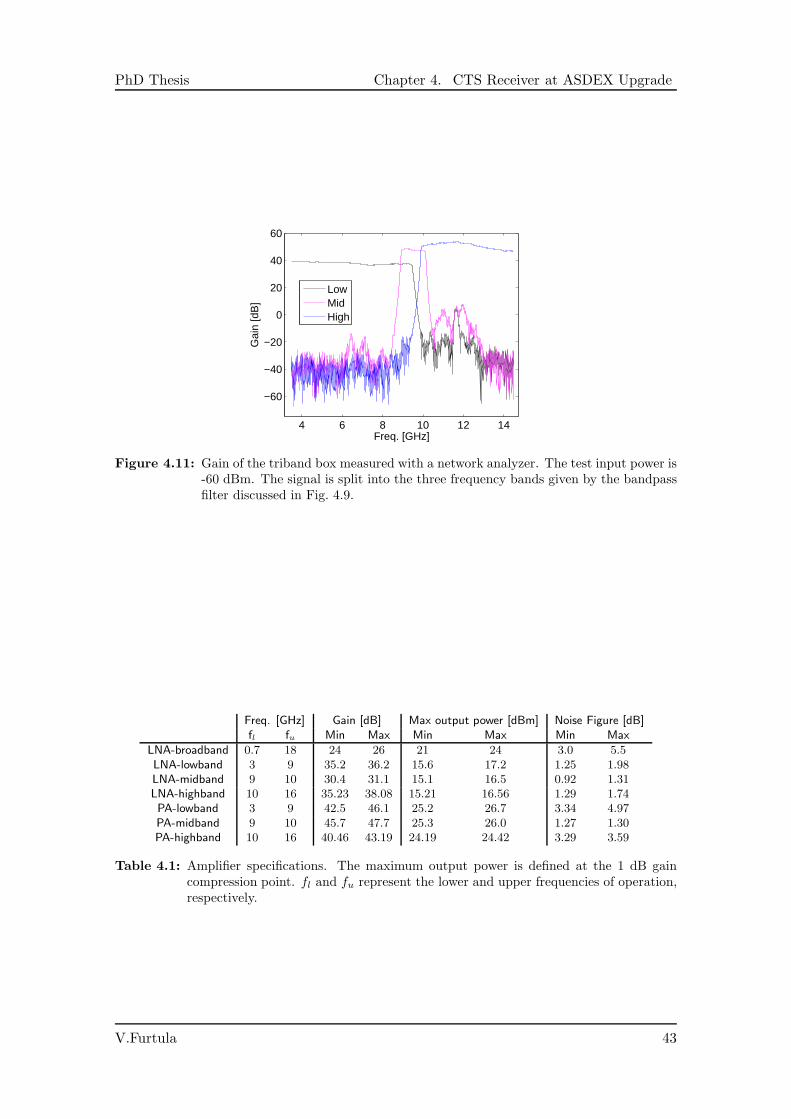
PhD Thesis Chapter 4. CTS Receiver at ASDEX Upgrade
4 6 8 10 12 14
−60
−40
−20
0
20
40
60
Freq. [GHz]
Gai
n [d
B]
LowMidHigh
Figure 4.11: Gain of the triband box measured with a network analyzer. The test input power is-60 dBm. The signal is split into the three frequency bands given by the bandpassfilter discussed in Fig. 4.9.
Freq. [GHz] Gain [dB] Max output power [dBm] Noise Figure [dB]fl fu Min Max Min Max Min Max
LNA-broadband 0.7 18 24 26 21 24 3.0 5.5LNA-lowband 3 9 35.2 36.2 15.6 17.2 1.25 1.98LNA-midband 9 10 30.4 31.1 15.1 16.5 0.92 1.31LNA-highband 10 16 35.23 38.08 15.21 16.56 1.29 1.74PA-lowband 3 9 42.5 46.1 25.2 26.7 3.34 4.97PA-midband 9 10 45.7 47.7 25.3 26.0 1.27 1.30PA-highband 10 16 40.46 43.19 24.19 24.42 3.29 3.59
Table 4.1: Amplifier specifications. The maximum output power is defined at the 1 dB gaincompression point. fl and fu represent the lower and upper frequencies of operation,respectively.
V.Furtula 43
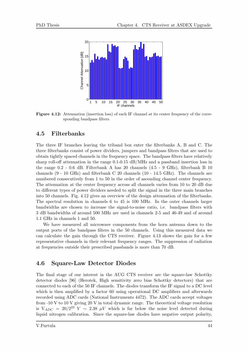
PhD Thesis Chapter 4. CTS Receiver at ASDEX Upgrade
1 5 10 15 20 25 30 35 40 45 500
5
10
15
20
Cha
nnel
Atte
nuat
ion
[dB
]
IF channels
Figure 4.12: Attenuation (insertion loss) of each IF channel at its center frequency of the corre-sponding bandpass filters.
4.5 Filterbanks
The three IF branches leaving the triband box enter the filterbanks A, B and C. Thethree filterbanks consist of power dividers, jumpers and bandpass filters that are used toobtain tightly spaced channels in the frequency space. The bandpass filters have relativelysharp roll-off attenuation in the range 0.1-0.15 dB/MHz and a passband insertion loss inthe range 0.2 - 0.6 dB. Filterbank A has 20 channels (4.5 - 9 GHz), filterbank B 10channels (9 - 10 GHz) and filterbank C 20 channels (10 - 14.5 GHz). The channels arenumbered consecutively from 1 to 50 in the order of ascending channel center frequency.The attenuation at the center frequency across all channels varies from 10 to 20 dB dueto different types of power dividers needed to split the signal in the three main branchesinto 50 channels. Fig. 4.12 gives an overview of the design attenuation of the filterbanks.The spectral resolution in channels 6 to 45 is 100 MHz. In the outer channels largerbandwidths are chosen to increase the signal-to-noise ratio, i.e. bandpass filters with3 dB bandwidths of around 500 MHz are used in channels 2-5 and 46-49 and of around1.1 GHz in channels 1 and 50.
We have measured all microwave components from the horn antenna down to theoutput ports of the bandpass filters in the 50 channels. Using this measured data wecan calculate the gain through the CTS receiver. Figure 4.13 shows the gain for a fewrepresentative channels in their relevant frequency ranges. The suppression of radiationat frequencies outside their prescribed passbands is more than 70 dB.
4.6 Square-Law Detector Diodes
The final stage of our interest in the AUG CTS receiver are the square-law Schottkydetector diodes [96] (Herotek, High sensitivity zero bias Schottky detectors) that areconnected to each of the 50 IF channels. The diodes transform the IF signal to a DC levelwhich is then amplified by a factor 60 using operational DC amplifiers and afterwardsrecorded using ADC cards (National Instruments 4472). The ADC cards accept voltagesfrom -10 V to 10 V giving 20 V in total dynamic range. The theoretical voltage resolutionis VADC = 20/223 V ∼ 2.38 µV which is far below the noise level detected duringliquid nitrogen calibration. Since the square-law diodes have negative output polarity,
V.Furtula 44
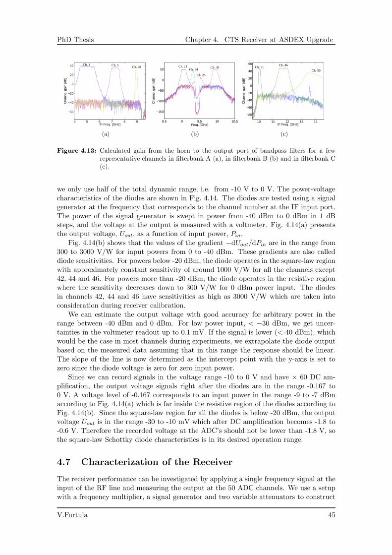
PhD Thesis Chapter 4. CTS Receiver at ASDEX Upgrade
4 5 6 7 8 9
−60
−40
−20
0
20
40C
hann
el g
ain
[dB
]
IF Freq. [GHz]
Ch. 1Ch. 20Ch. 5
(a)
8.5 9 9.5 10 10.5
−150
−100
−50
0
50
Cha
nnel
gai
n [d
B]
Freq. [GHz]
Ch. 21Ch. 24
Ch. 25
Ch. 30
(b)
10 11 12 13 14
−80
−60
−40
−20
0
20
40
60
Cha
nnel
gai
n [d
B]
IF Freq. [GHz]
Ch. 46
Ch. 50Ch. 31
(c)
Figure 4.13: Calculated gain from the horn to the output port of bandpass filters for a fewrepresentative channels in filterbank A (a), in filterbank B (b) and in filterbank C(c).
we only use half of the total dynamic range, i.e. from -10 V to 0 V. The power-voltagecharacteristics of the diodes are shown in Fig. 4.14. The diodes are tested using a signalgenerator at the frequency that corresponds to the channel number at the IF input port.The power of the signal generator is swept in power from -40 dBm to 0 dBm in 1 dBsteps, and the voltage at the output is measured with a voltmeter. Fig. 4.14(a) presentsthe output voltage, Uout, as a function of input power, Pin.
Fig. 4.14(b) shows that the values of the gradient −dUout/dPin are in the range from300 to 3000 V/W for input powers from 0 to -40 dBm. These gradients are also calleddiode sensitivities. For powers below -20 dBm, the diode operates in the square-law regionwith approximately constant sensitivity of around 1000 V/W for all the channels except42, 44 and 46. For powers more than -20 dBm, the diode operates in the resistive regionwhere the sensitivity decreases down to 300 V/W for 0 dBm power input. The diodesin channels 42, 44 and 46 have sensitivities as high as 3000 V/W which are taken intoconsideration during receiver calibration.
We can estimate the output voltage with good accuracy for arbitrary power in therange between -40 dBm and 0 dBm. For low power input, < −30 dBm, we get uncer-tainties in the voltmeter readout up to 0.1 mV. If the signal is lower (<-40 dBm), whichwould be the case in most channels during experiments, we extrapolate the diode outputbased on the measured data assuming that in this range the response should be linear.The slope of the line is now determined as the intercept point with the y-axis is set tozero since the diode voltage is zero for zero input power.
Since we can record signals in the voltage range -10 to 0 V and have × 60 DC am-plification, the output voltage signals right after the diodes are in the range -0.167 to0 V. A voltage level of -0.167 corresponds to an input power in the range -9 to -7 dBmaccording to Fig. 4.14(a) which is far inside the resistive region of the diodes according toFig. 4.14(b). Since the square-law region for all the diodes is below -20 dBm, the outputvoltage Uout is in the range -30 to -10 mV which after DC amplification becomes -1.8 to-0.6 V. Therefore the recorded voltage at the ADC’s should not be lower than -1.8 V, sothe square-law Schottky diode characteristics is in its desired operation range.
4.7 Characterization of the Receiver
The receiver performance can be investigated by applying a single frequency signal at theinput of the RF line and measuring the output at the 50 ADC channels. We use a setupwith a frequency multiplier, a signal generator and two variable attenuators to construct
V.Furtula 45
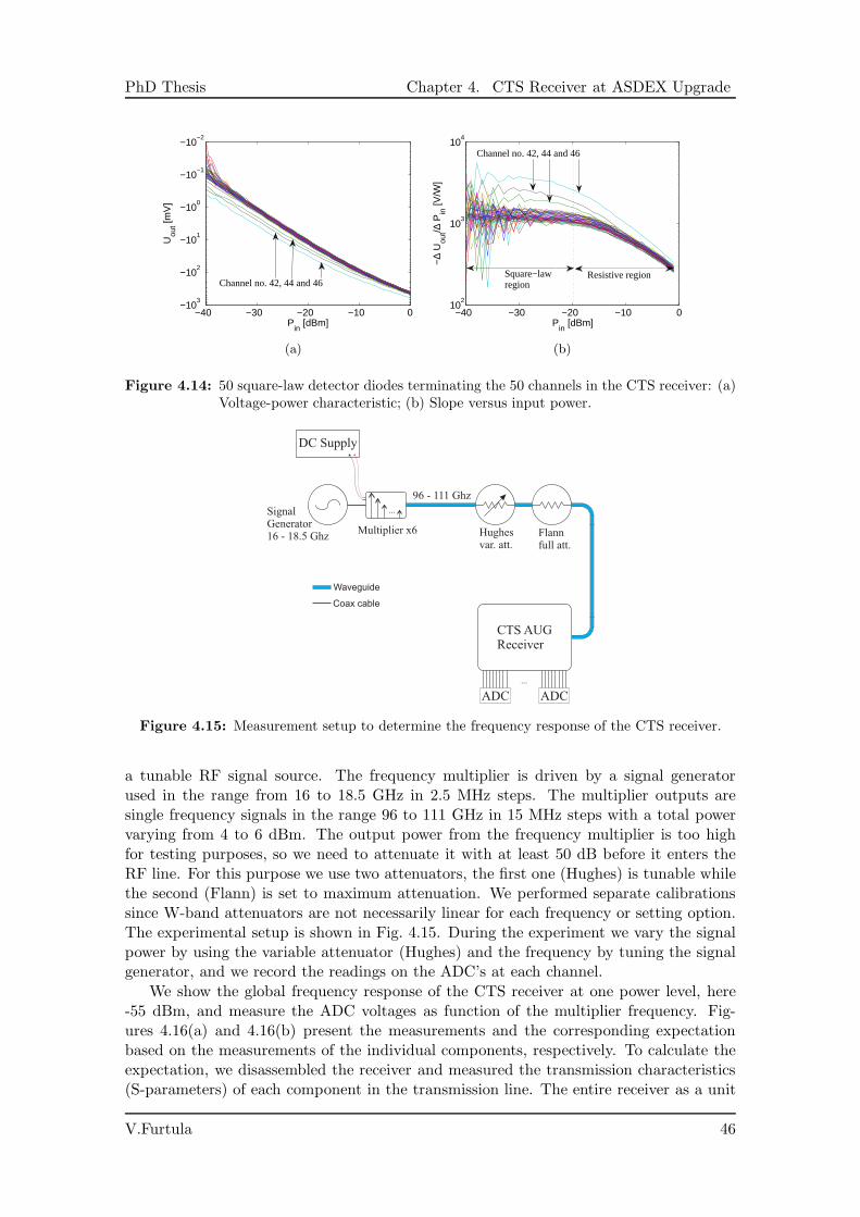
PhD Thesis Chapter 4. CTS Receiver at ASDEX Upgrade
−40 −30 −20 −10 0−10
3
−102
−101
−100
−10−1
−10−2
Pin
[dBm]
Uou
t [mV
]
Channel no. 42, 44 and 46
(a)
−40 −30 −20 −10 010
2
103
104
Pin
[dBm]
−∆
Uou
t/∆ P
in [V
/W]
Channel no. 42, 44 and 46
Square−lawregion
Resistive region
(b)
Figure 4.14: 50 square-law detector diodes terminating the 50 channels in the CTS receiver: (a)Voltage-power characteristic; (b) Slope versus input power.
Figure 4.15: Measurement setup to determine the frequency response of the CTS receiver.
a tunable RF signal source. The frequency multiplier is driven by a signal generatorused in the range from 16 to 18.5 GHz in 2.5 MHz steps. The multiplier outputs aresingle frequency signals in the range 96 to 111 GHz in 15 MHz steps with a total powervarying from 4 to 6 dBm. The output power from the frequency multiplier is too highfor testing purposes, so we need to attenuate it with at least 50 dB before it enters theRF line. For this purpose we use two attenuators, the first one (Hughes) is tunable whilethe second (Flann) is set to maximum attenuation. We performed separate calibrationssince W-band attenuators are not necessarily linear for each frequency or setting option.The experimental setup is shown in Fig. 4.15. During the experiment we vary the signalpower by using the variable attenuator (Hughes) and the frequency by tuning the signalgenerator, and we record the readings on the ADC’s at each channel.
We show the global frequency response of the CTS receiver at one power level, here-55 dBm, and measure the ADC voltages as function of the multiplier frequency. Fig-ures 4.16(a) and 4.16(b) present the measurements and the corresponding expectationbased on the measurements of the individual components, respectively. To calculate theexpectation, we disassembled the receiver and measured the transmission characteristics(S-parameters) of each component in the transmission line. The entire receiver as a unit
V.Furtula 46
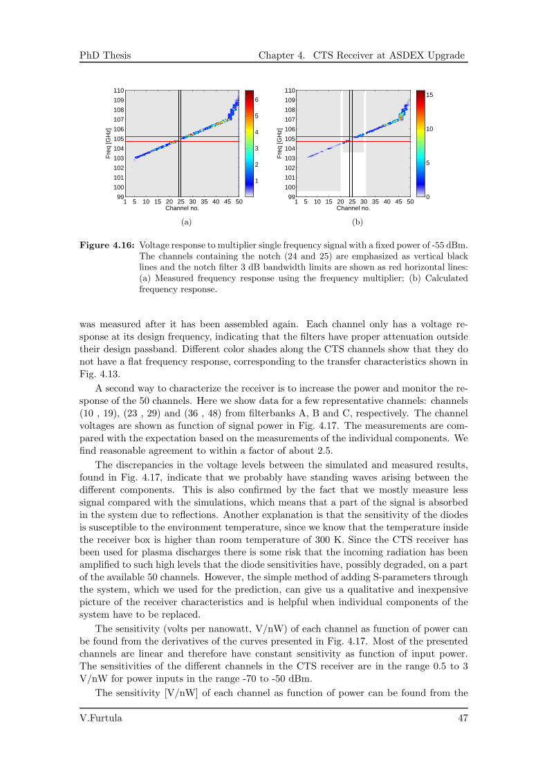
PhD Thesis Chapter 4. CTS Receiver at ASDEX Upgrade
Channel no.
Fre
q [G
Hz]
1 5 10 15 20 25 30 35 40 45 5099
100
101
102
103
104
105
106
107
108
109
110
1
2
3
4
5
6
(a)
Channel no.
Fre
q [G
Hz]
1 5 10 15 20 25 30 35 40 45 5099
100
101
102
103
104
105
106
107
108
109
110
0
5
10
15
(b)
Figure 4.16: Voltage response to multiplier single frequency signal with a fixed power of -55 dBm.The channels containing the notch (24 and 25) are emphasized as vertical blacklines and the notch filter 3 dB bandwidth limits are shown as red horizontal lines:(a) Measured frequency response using the frequency multiplier; (b) Calculatedfrequency response.
was measured after it has been assembled again. Each channel only has a voltage re-sponse at its design frequency, indicating that the filters have proper attenuation outsidetheir design passband. Different color shades along the CTS channels show that they donot have a flat frequency response, corresponding to the transfer characteristics shown inFig. 4.13.
A second way to characterize the receiver is to increase the power and monitor the re-sponse of the 50 channels. Here we show data for a few representative channels: channels(10 , 19), (23 , 29) and (36 , 48) from filterbanks A, B and C, respectively. The channelvoltages are shown as function of signal power in Fig. 4.17. The measurements are com-pared with the expectation based on the measurements of the individual components. Wefind reasonable agreement to within a factor of about 2.5.
The discrepancies in the voltage levels between the simulated and measured results,found in Fig. 4.17, indicate that we probably have standing waves arising between thedifferent components. This is also confirmed by the fact that we mostly measure lesssignal compared with the simulations, which means that a part of the signal is absorbedin the system due to reflections. Another explanation is that the sensitivity of the diodesis susceptible to the environment temperature, since we know that the temperature insidethe receiver box is higher than room temperature of 300 K. Since the CTS receiver hasbeen used for plasma discharges there is some risk that the incoming radiation has beenamplified to such high levels that the diode sensitivities have, possibly degraded, on a partof the available 50 channels. However, the simple method of adding S-parameters throughthe system, which we used for the prediction, can give us a qualitative and inexpensivepicture of the receiver characteristics and is helpful when individual components of thesystem have to be replaced.
The sensitivity (volts per nanowatt, V/nW) of each channel as function of power canbe found from the derivatives of the curves presented in Fig. 4.17. Most of the presentedchannels are linear and therefore have constant sensitivity as function of input power.The sensitivities of the different channels in the CTS receiver are in the range 0.5 to 3V/nW for power inputs in the range -70 to -50 dBm.
The sensitivity [V/nW] of each channel as function of power can be found from the
V.Furtula 47
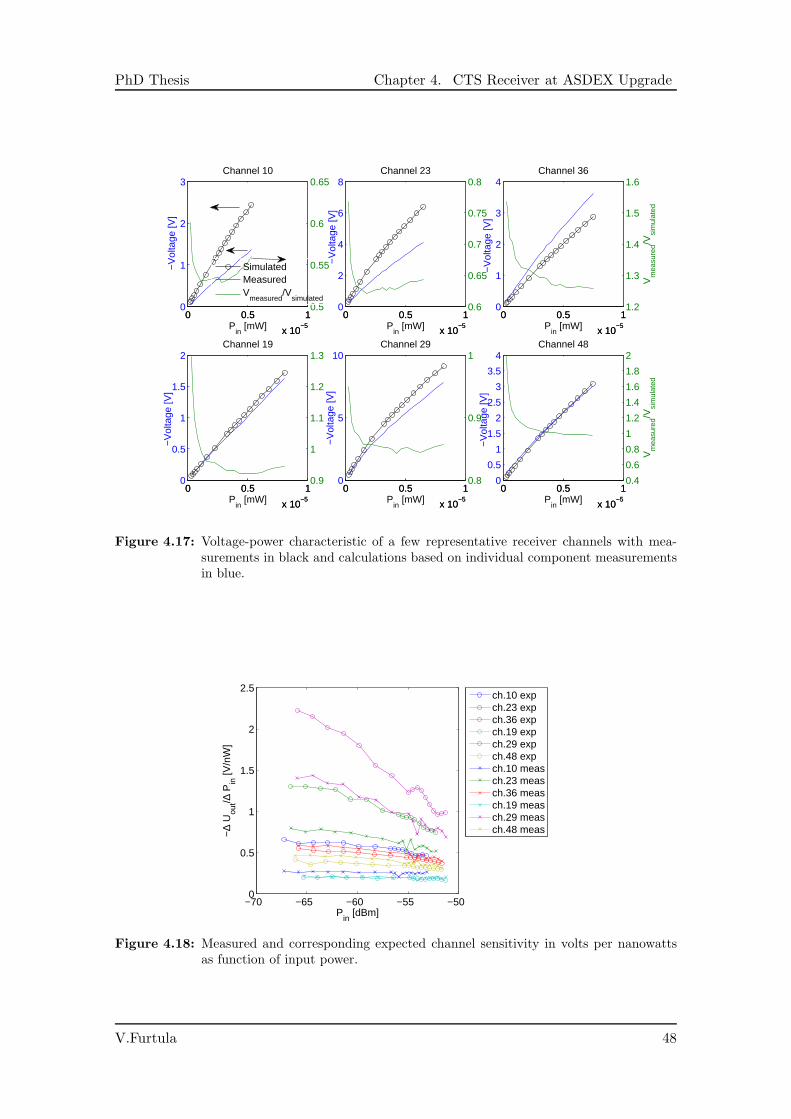
PhD Thesis Chapter 4. CTS Receiver at ASDEX Upgrade
0 0.5 1
x 10−5
0
1
2
3Channel 10
−V
olta
ge [V
]
Pin
[mW]
0 0.5 1
x 10−5
0.5
0.55
0.6
0.65
SimulatedMeasuredV
measured/V
simulated
0 0.5 1
x 10−5
0
0.5
1
1.5
2Channel 19
−V
olta
ge [V
]
Pin
[mW]0 0.5 1
x 10−5
0.9
1
1.1
1.2
1.3
0 0.5 1
x 10−5
0
2
4
6
8Channel 23
−V
olta
ge [V
]P
in [mW]
0 0.5 1
x 10−5
0.6
0.65
0.7
0.75
0.8
0 0.5 1
x 10−5
0
5
10Channel 29
−V
olta
ge [V
]
Pin
[mW]0 0.5 1
x 10−5
0.8
0.9
1
0 0.5 1
x 10−5
0
1
2
3
4Channel 36
−V
olta
ge [V
]
Pin
[mW]0 0.5 1
x 10−5
1.2
1.3
1.4
1.5
1.6
Vm
easu
red/V
sim
ulat
ed
0 0.5 1
x 10−5
0
0.5
1
1.5
2
2.5
3
3.5
4Channel 48
−V
olta
ge [V
]
Pin
[mW]0 0.5 1
x 10−5
0.4
0.6
0.8
1
1.2
1.4
1.6
1.8
2
Vm
easu
red/V
sim
ulat
ed
Figure 4.17: Voltage-power characteristic of a few representative receiver channels with mea-surements in black and calculations based on individual component measurementsin blue.
−70 −65 −60 −55 −500
0.5
1
1.5
2
2.5
Pin
[dBm]
−∆
Uou
t/∆ P
in [V
/nW
]
ch.10 expch.23 expch.36 expch.19 expch.29 expch.48 expch.10 measch.23 measch.36 measch.19 measch.29 measch.48 meas
Figure 4.18: Measured and corresponding expected channel sensitivity in volts per nanowattsas function of input power.
V.Furtula 48
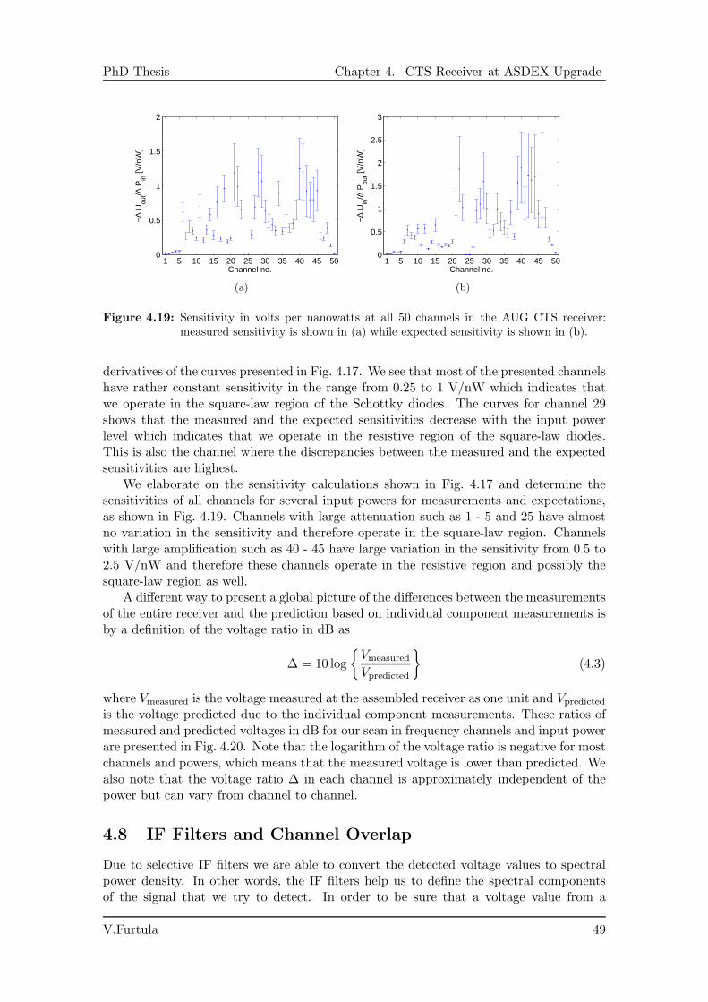
PhD Thesis Chapter 4. CTS Receiver at ASDEX Upgrade
1 5 10 15 20 25 30 35 40 45 500
0.5
1
1.5
2
Channel no.
−∆
Uou
t/∆ P
in [V
/nW
]
(a)
1 5 10 15 20 25 30 35 40 45 500
0.5
1
1.5
2
2.5
3
Channel no.
−∆
Uin
/∆ P
out [V
/nW
]
(b)
Figure 4.19: Sensitivity in volts per nanowatts at all 50 channels in the AUG CTS receiver:measured sensitivity is shown in (a) while expected sensitivity is shown in (b).
derivatives of the curves presented in Fig. 4.17. We see that most of the presented channelshave rather constant sensitivity in the range from 0.25 to 1 V/nW which indicates thatwe operate in the square-law region of the Schottky diodes. The curves for channel 29shows that the measured and the expected sensitivities decrease with the input powerlevel which indicates that we operate in the resistive region of the square-law diodes.This is also the channel where the discrepancies between the measured and the expectedsensitivities are highest.
We elaborate on the sensitivity calculations shown in Fig. 4.17 and determine thesensitivities of all channels for several input powers for measurements and expectations,as shown in Fig. 4.19. Channels with large attenuation such as 1 - 5 and 25 have almostno variation in the sensitivity and therefore operate in the square-law region. Channelswith large amplification such as 40 - 45 have large variation in the sensitivity from 0.5 to2.5 V/nW and therefore these channels operate in the resistive region and possibly thesquare-law region as well.
A different way to present a global picture of the differences between the measurementsof the entire receiver and the prediction based on individual component measurements isby a definition of the voltage ratio in dB as
∆ = 10 log
Vmeasured
Vpredicted
(4.3)
where Vmeasured is the voltage measured at the assembled receiver as one unit and Vpredictedis the voltage predicted due to the individual component measurements. These ratios ofmeasured and predicted voltages in dB for our scan in frequency channels and input powerare presented in Fig. 4.20. Note that the logarithm of the voltage ratio is negative for mostchannels and powers, which means that the measured voltage is lower than predicted. Wealso note that the voltage ratio ∆ in each channel is approximately independent of thepower but can vary from channel to channel.
4.8 IF Filters and Channel Overlap
Due to selective IF filters we are able to convert the detected voltage values to spectralpower density. In other words, the IF filters help us to define the spectral componentsof the signal that we try to detect. In order to be sure that a voltage value from a
V.Furtula 49
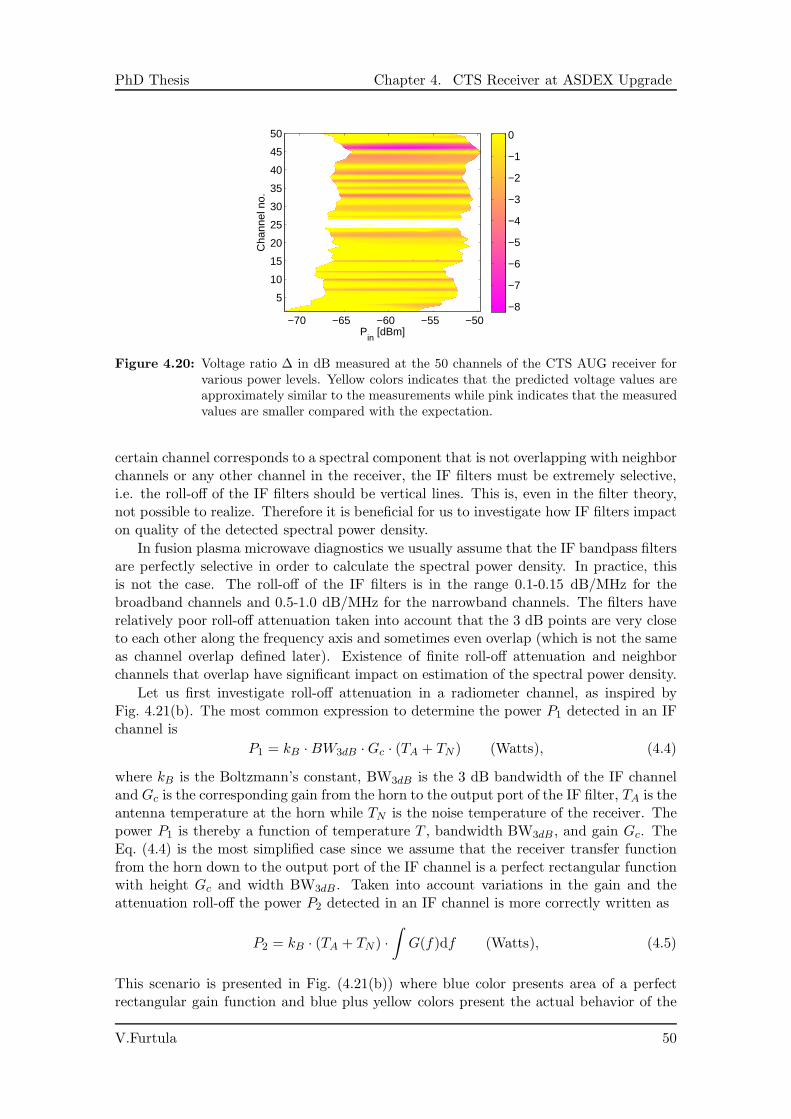
PhD Thesis Chapter 4. CTS Receiver at ASDEX Upgrade
Cha
nnel
no.
Pin
[dBm]
−70 −65 −60 −55 −50
5
10
15
20
25
30
35
40
45
50
−8
−7
−6
−5
−4
−3
−2
−1
0
Figure 4.20: Voltage ratio ∆ in dB measured at the 50 channels of the CTS AUG receiver forvarious power levels. Yellow colors indicates that the predicted voltage values areapproximately similar to the measurements while pink indicates that the measuredvalues are smaller compared with the expectation.
certain channel corresponds to a spectral component that is not overlapping with neighborchannels or any other channel in the receiver, the IF filters must be extremely selective,i.e. the roll-off of the IF filters should be vertical lines. This is, even in the filter theory,not possible to realize. Therefore it is beneficial for us to investigate how IF filters impacton quality of the detected spectral power density.
In fusion plasma microwave diagnostics we usually assume that the IF bandpass filtersare perfectly selective in order to calculate the spectral power density. In practice, thisis not the case. The roll-off of the IF filters is in the range 0.1-0.15 dB/MHz for thebroadband channels and 0.5-1.0 dB/MHz for the narrowband channels. The filters haverelatively poor roll-off attenuation taken into account that the 3 dB points are very closeto each other along the frequency axis and sometimes even overlap (which is not the sameas channel overlap defined later). Existence of finite roll-off attenuation and neighborchannels that overlap have significant impact on estimation of the spectral power density.
Let us first investigate roll-off attenuation in a radiometer channel, as inspired byFig. 4.21(b). The most common expression to determine the power P1 detected in an IFchannel is
P1 = kB ·BW3dB ·Gc · (TA + TN ) (Watts), (4.4)
where kB is the Boltzmann’s constant, BW3dB is the 3 dB bandwidth of the IF channeland Gc is the corresponding gain from the horn to the output port of the IF filter, TA is theantenna temperature at the horn while TN is the noise temperature of the receiver. Thepower P1 is thereby a function of temperature T , bandwidth BW3dB , and gain Gc. TheEq. (4.4) is the most simplified case since we assume that the receiver transfer functionfrom the horn down to the output port of the IF channel is a perfect rectangular functionwith height Gc and width BW3dB . Taken into account variations in the gain and theattenuation roll-off the power P2 detected in an IF channel is more correctly written as
P2 = kB · (TA + TN ) ·∫
G(f)df (Watts), (4.5)
This scenario is presented in Fig. (4.21(b)) where blue color presents area of a perfectrectangular gain function and blue plus yellow colors present the actual behavior of the
V.Furtula 50
PhD Thesis Chapter 4. CTS Receiver at ASDEX Upgrade
transfer function with gain variation and attenuation roll-off. Figure 4.22 shows exampleson measured gain functions versus frequency for filterbanks A and C, respectively, wherelarge channel overlaps supported by attenuation roll-of are clearly seen. By dividing theEq. 4.4 with Eq. (4.5) we get
Channel ratio =P2 − P1
P2= 1− BW3dB ·Gc
∫
G(f)df. (4.6)
Applying all the transfer function measurements of the CTS radiometer into Eq. (4.6) weget an output shown as the red curve in Fig. 4.23. The red curve clearly shows that simpleassumption from Eq. (4.4) will underestimate the total integrated power in each channelby 10 - 20%. Converting this result into the terms of a perfect rectangular function withheight Gc and width BW3dB , we can state that the absolute 3 dB bandwidth is a bitbroader than BW3dB defined in Eq. 4.4.
Since we have measured all the IF filters we can also determine the overlap area ofa channel with its two nearest neighbor channels. Since we do not have theoretical gaintransfer functions available we need to use logical statements in order to find overlapareas that are common to neighbor channels and the channel in consideration as shown inFig. 4.21(a). Caution needs to be taken during overlap area calculation since for instancechannels 1 and 3 may have a large overlap that is placed inside channel 2. Therefore allthe overlap calculations are divided into the region below the point where channel 1 and3 cross and the region after channel 1 and 3 cross. This procedure is repeated exactly thesame way for channels 2, 3, and 4 etc. with the channel overlap ratio presented as theblue curve in Fig. 4.23. The information contained in the blue curve can be interpreted asfollows; values around zero indicate channels that are spectrally divided very well, whilevalues around one indicate channels that are poorly spectrally divided. In our case wehave a surprising result showing us in average around 50% of overlap signal across allchannels. In other words, 50% of the signal we detect in one channel can also be found inthe two neighbor channels, i.e. the channels that are close to each other are also stronglycorrelated. The worst case scenario with overlap larger than 80 % is seen in channels 6and 45, and naturally in channels 24 and 25 which correspond to notch filter channels.Thereby, channels such as 6 and 45 have very little information that are unique and notshown in any neighbor channels. Poor spectral selection of the IF filters increase thecost of the receiver and at the same time it limits the dynamic resolution of the spectralpower density because channel overlap areas are too large. Notice that the knowledgeof channel overlap ratio does not necessarily uncover more information on attenuationroll-off or gain variation in the channels, for that we need to have transfer function versusfrequency available.
4.9 Conclusions
The individual components of the CTS receiver at ASDEX Upgrade and their performancecharacteristics are presented. The receiver uses a heterodyne scheme, i.e. converts signalsin the W-band down to IF signals in a down-mixing stage. We find losses in the range 10 to26 dB in the receiver RF line which is sometimes inevitable due to filtering requirements.The mixer has conversion losses in the range from 5 to 6 dB which adds to the receivernoise figure. The down-converted IF signal is amplified and divided into three bandsusing three bandpass filters in the triband box. There are two further amplifiers in eachbranch of the triband box, making it seven amplifiers in total. Thereby every branchhas three amplifiers in cascade of which the first one is common for all three branches.
V.Furtula 51

PhD Thesis Chapter 4. CTS Receiver at ASDEX Upgrade
Ch. 1
Freq
Channel gainCh. 3
Ch. 2
Channel overlap
...
(a)
Ch. 1
Freq
Channel gainCh. 3
Ch. 2
...
(b)
Figure 4.21: Overlap area between the neighbor channels is shown in (a) while simple integrationcovering spectrum defined by 3 dB points is shown in (b).
7.4 7.6 7.8 80
20
40
60
80
Cha
nnel
gai
n
Freq. [GHz]
Ch. 6 Ch. 8Ch. 7Ch. 5
(a)
11.2 11.4 11.6 11.8 120
50
100
150
200C
hann
el g
ain
Freq. [GHz]
Ch. 44
Ch. 45
Ch. 46
Ch. 43
(b)
Figure 4.22: Gain for channels in the filterbank A shown in (a) while gain for channels in thefilterbank C shown in (b). The curves for channels presented in both graphs arelinear in scale and calculated on basis of voltage gain.
0 10 20 30 40 500
0.2
0.4
0.6
0.8
1
Channel No.
Cha
nnel
ove
rlap
ratio
Simple integrationChannel overlap
Ch. 45
Ch. 6
Figure 4.23: Channel overlap ratio.
V.Furtula 52
PhD Thesis Chapter 4. CTS Receiver at ASDEX Upgrade
The amplifiers have gain in the range from 24 to 46 dB and power output at 1 dB gaincompression from 15 to 27 dBm. The IF filterbanks A, B and C containing 50 bandpassfilters will assure passage of signals in the frequency range from 4.5 to 14.5 GHz, eachchannel only in its design frequency bandwidth of typically 100 MHz. Schottky square-law detector diodes are used to convert the IF signal down to DC voltage levels whichare acquired by 24 bit acquisition cards. They operate in the square-law region for inputpowers up to -20 dBm. Their sensitivity in this region varies from 900 to 1300 V/W. Thetotal receiver noise figure is frequency dependent and in the range between 11 and 20 dBexcept for in the notch filter channels. The largest contributions to the noise figure arethe losses in the RF-line and the mixer conversion loss.
The characterization of the individual components allows us to calculate the receiverresponse to RF signals at various frequencies. This expectation of the receiver response iscompared with the measured receiver response. To measure the entire receiver response,we use a signal generator and a frequency multiplier as a tunable single frequency signalsource and a variable attenuator to control the output power. A scan with varyingRF frequency and power has been performed. The measurement of the entire receiverresponse agrees reasonably well with the expectation based on the individual componentmeasurements within a factor of about 2.5. In both measurement methods we find thatthe voltage response across channels is not flat and can vary by several volts. Generationof harmonics in the mixer or amplifiers and radiation leakage are well suppressed in thepresent CTS receiver design.
We have calculated the sensitivity as function of input power for all 50 channels formeasurements as well as for the expectations. For the channels with low amplification thesensitivity is relatively constant. For most of the channels we find that the sensitivity isin the range from 0.5 to 3 V/nW for the measurements and expectations. Furthermore,we have investigated the influence of the finite filter roll-off attenuation on the powerdetected at the channels. From the system point of view, we find it acceptable to useindividual component measurements to predict the overall performance of the CTS AUGreceiver.
V.Furtula 53

Chapter 5
Notch Filter Design
5.1 Short background and introduction
Due to large stray radiation and frequency drift of the probing beam we find it necessaryto design and build these filters in our lab facilities. We have made several designs onnotch filters based on two different approaches. Both approaches are based on the sametechnology where we use cylindrical stubs as resonators connected to the main waveguideby narrow apertures. The difference in these two approaches is the orientation of theresonators relative to the main waveguide.
Since the Danish CTS group is abundantly involved in the campaigns at ASDEXUpgrade five notch filters have been designed to support the ongoing experimental work.Two notch filters with 105 GHz center frequency, more than 20 GHz passband coverage,and 1 GHz rejection bandwidth have been constructed. One of the filters is based ona rectangular waveguide with cylindrical cavities coupled by narrow iris gaps, i.e. smallelongated holes of negligible thickness. The other filter is based on approach by aperturecoupling using thin slits. Furthermore, a notch filter for the ECE group at ASDEXUpgrade, based on aperture coupling using thin slits, 140 GHz center frequency, and1 GHz rejection bandwidth has been designed and tested. The two last notch filters with105 GHz center frequency and only 100 MHz rejection bandwidth were designed andtested for the newly installed CTS receiver at ASDEX Upgrade.
We use numerical simulations to study the sensitivity of the notch filter performanceto changes in geometry and in material conductivity. The constructed filters are testedsuccessfully using a self-made measurement setup or a commercial vector network analyzermonitoring bandwidths from 10 and up to 20 GHz. The typical insertion loss in thepassband is below 1.5 dB while the attenuation in the stopband is varying from 40 dBand up to 90 dB, depending on the approach and number of the resonators used. Extensiveaspects on coupled cavity resonators are presented in [11, 65, 51].
5.2 105 GHz notch filter for CTS
In magnetic confinement devices, such as tokamaks or stellarators, mm-wave notch filtersare used to protect diagnostic instruments from gyrotron stray radiation. Typical mm-wave diagnostics are ECE spectroscopy, reflectometry, and CTS [48]. Gyrotrons producehigh power mm-waves and are used for electron cyclotron resonance heating (ECRH)and current drive (ECCD) [89, 88], for mitigation of tearing modes [91], and as a probingradiation source in CTS experiments [53, 54, 70]. Notch filters can make mm-wave plasmadiagnostics compatible to plasma experiments with gyrotron operation.
55
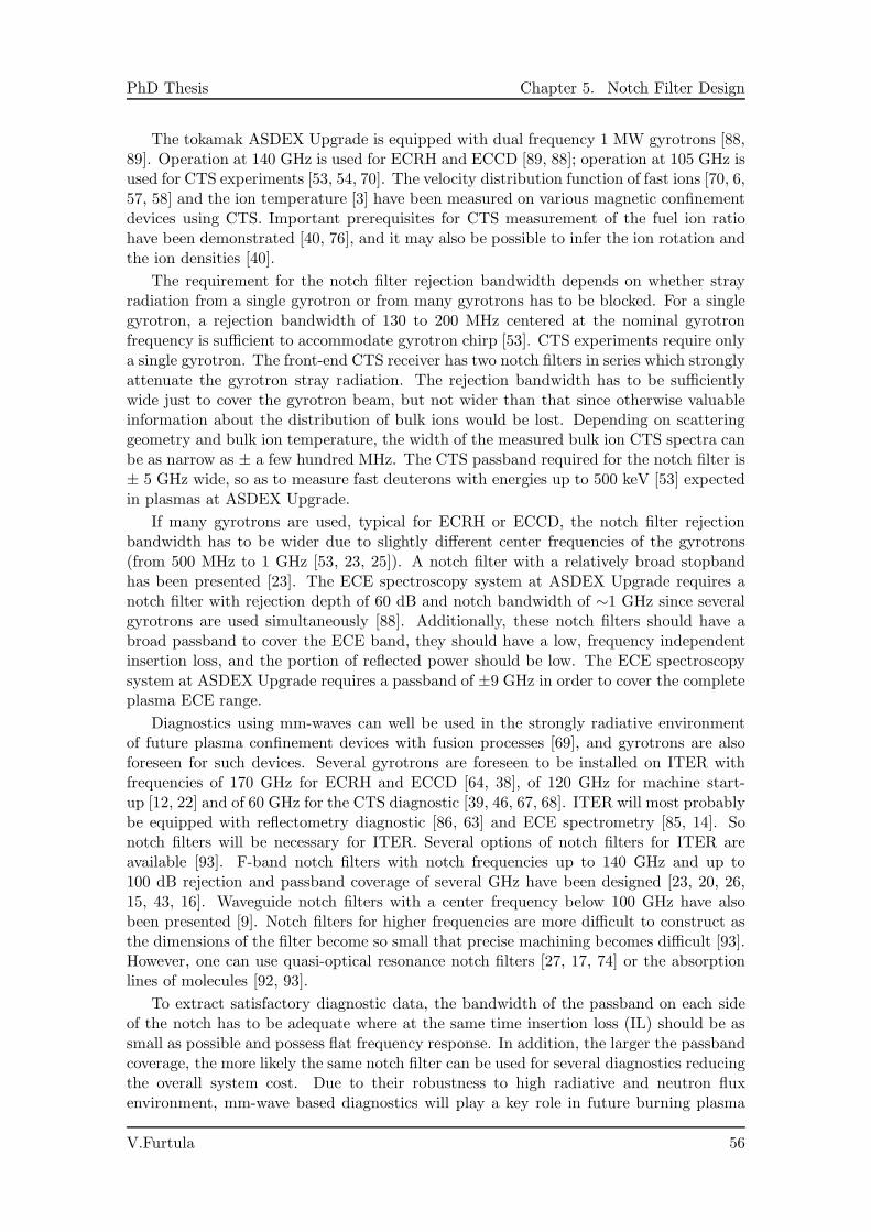
PhD Thesis Chapter 5. Notch Filter Design
The tokamak ASDEX Upgrade is equipped with dual frequency 1 MW gyrotrons [88,89]. Operation at 140 GHz is used for ECRH and ECCD [89, 88]; operation at 105 GHz isused for CTS experiments [53, 54, 70]. The velocity distribution function of fast ions [70, 6,57, 58] and the ion temperature [3] have been measured on various magnetic confinementdevices using CTS. Important prerequisites for CTS measurement of the fuel ion ratiohave been demonstrated [40, 76], and it may also be possible to infer the ion rotation andthe ion densities [40].
The requirement for the notch filter rejection bandwidth depends on whether strayradiation from a single gyrotron or from many gyrotrons has to be blocked. For a singlegyrotron, a rejection bandwidth of 130 to 200 MHz centered at the nominal gyrotronfrequency is sufficient to accommodate gyrotron chirp [53]. CTS experiments require onlya single gyrotron. The front-end CTS receiver has two notch filters in series which stronglyattenuate the gyrotron stray radiation. The rejection bandwidth has to be sufficientlywide just to cover the gyrotron beam, but not wider than that since otherwise valuableinformation about the distribution of bulk ions would be lost. Depending on scatteringgeometry and bulk ion temperature, the width of the measured bulk ion CTS spectra canbe as narrow as ± a few hundred MHz. The CTS passband required for the notch filter is± 5 GHz wide, so as to measure fast deuterons with energies up to 500 keV [53] expectedin plasmas at ASDEX Upgrade.
If many gyrotrons are used, typical for ECRH or ECCD, the notch filter rejectionbandwidth has to be wider due to slightly different center frequencies of the gyrotrons(from 500 MHz to 1 GHz [53, 23, 25]). A notch filter with a relatively broad stopbandhas been presented [23]. The ECE spectroscopy system at ASDEX Upgrade requires anotch filter with rejection depth of 60 dB and notch bandwidth of ∼1 GHz since severalgyrotrons are used simultaneously [88]. Additionally, these notch filters should have abroad passband to cover the ECE band, they should have a low, frequency independentinsertion loss, and the portion of reflected power should be low. The ECE spectroscopysystem at ASDEX Upgrade requires a passband of ±9 GHz in order to cover the completeplasma ECE range.
Diagnostics using mm-waves can well be used in the strongly radiative environmentof future plasma confinement devices with fusion processes [69], and gyrotrons are alsoforeseen for such devices. Several gyrotrons are foreseen to be installed on ITER withfrequencies of 170 GHz for ECRH and ECCD [64, 38], of 120 GHz for machine start-up [12, 22] and of 60 GHz for the CTS diagnostic [39, 46, 67, 68]. ITER will most probablybe equipped with reflectometry diagnostic [86, 63] and ECE spectrometry [85, 14]. Sonotch filters will be necessary for ITER. Several options of notch filters for ITER areavailable [93]. F-band notch filters with notch frequencies up to 140 GHz and up to100 dB rejection and passband coverage of several GHz have been designed [23, 20, 26,15, 43, 16]. Waveguide notch filters with a center frequency below 100 GHz have alsobeen presented [9]. Notch filters for higher frequencies are more difficult to construct asthe dimensions of the filter become so small that precise machining becomes difficult [93].However, one can use quasi-optical resonance notch filters [27, 17, 74] or the absorptionlines of molecules [92, 93].
To extract satisfactory diagnostic data, the bandwidth of the passband on each sideof the notch has to be adequate where at the same time insertion loss (IL) should be assmall as possible and possess flat frequency response. In addition, the larger the passbandcoverage, the more likely the same notch filter can be used for several diagnostics reducingthe overall system cost. Due to their robustness to high radiative and neutron fluxenvironment, mm-wave based diagnostics will play a key role in future burning plasma
V.Furtula 56
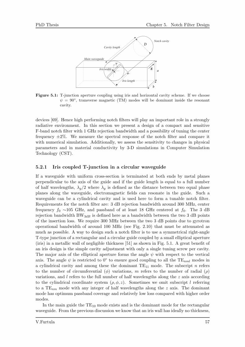
PhD Thesis Chapter 5. Notch Filter Design
Iris length
E
Main waveguide
Notch cavity
Iris width
b
a
ψ
Cavity length
Figure 5.1: T-junction aperture coupling using iris and horizontal cavity scheme. If we chooseψ = 90, transverse magnetic (TM) modes will be dominant inside the resonantcavity.
devices [69]. Hence high performing notch filters will play an important role in a stronglyradiative environment. In this section we present a design of a compact and sensitiveF-band notch filter with 1 GHz rejection bandwidth and a possibility of tuning the centerfrequency ±2%. We measure the spectral response of the notch filter and compare itwith numerical simulation. Additionally, we assess the sensitivity to changes in physicalparameters and in material conductivity by 3-D simulations in Computer SimulationTechnology (CST).
5.2.1 Iris coupled T-junction in a circular waveguide
If a waveguide with uniform cross-section is terminated at both ends by metal planesperpendicular to the axis of the guide and if the guide length is equal to a full numberof half wavelengths, λg/2 where λg is defined as the distance between two equal phaseplanes along the waveguide, electromagnetic fields can resonate in the guide. Such awaveguide can be a cylindrical cavity and is used here to form a tunable notch filter.Requirements for the notch filter are: 3 dB rejection bandwidth around 300 MHz, centerfrequency f0 ∼105 GHz, and passband of at least 18 GHz centered at f0. The 3 dBrejection bandwidth BW3dB is defined here as a bandwidth between the two 3 dB pointsof the insertion loss. We require 300 MHz between the two 3 dB points due to gyrotronoperational bandwidth of around 100 MHz (see Fig. 2.10) that must be attenuated asmuch as possible. A way to design such a notch filter is to use a symmetrical right-angleT-type junction of a rectangular and a circular guide coupled by a small elliptical aperture(iris) in a metallic wall of negligible thickness [51] as shown in Fig. 5.1. A great benefit ofan iris design is the simple cavity adjustment with only a single tuning screw per cavity.The major axis of the elliptical aperture forms the angle ψ with respect to the verticalaxis. The angle ψ is restricted to 0 to ensure good coupling to all the TEnml modes ina cylindrical cavity and among these the dominant TE11 mode. The subscript n refersto the number of circumferential (φ) variations, m refers to the number of radial (ρ)variations, and l refers to the full number of half wavelengths along the z axis accordingto the cylindrical coordinate system (ρ, φ, z). Sometimes we omit subscript l referringto a TEnm mode with any integer of half wavelengths along the z axis. The dominantmode has optimum passband coverage and relatively low loss compared with higher ordermodes.
In the main guide the TE10 mode exists and is the dominant mode for the rectangularwaveguide. From the previous discussion we know that an iris wall has ideally no thickness,
V.Furtula 57
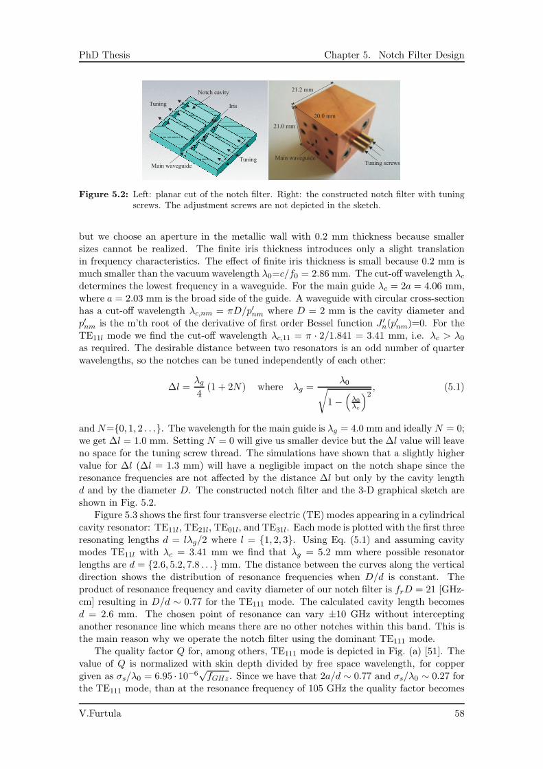
PhD Thesis Chapter 5. Notch Filter Design
Figure 5.2: Left: planar cut of the notch filter. Right: the constructed notch filter with tuningscrews. The adjustment screws are not depicted in the sketch.
but we choose an aperture in the metallic wall with 0.2 mm thickness because smallersizes cannot be realized. The finite iris thickness introduces only a slight translationin frequency characteristics. The effect of finite iris thickness is small because 0.2 mm ismuch smaller than the vacuum wavelength λ0=c/f0 = 2.86 mm. The cut-off wavelength λcdetermines the lowest frequency in a waveguide. For the main guide λc = 2a = 4.06 mm,where a = 2.03 mm is the broad side of the guide. A waveguide with circular cross-sectionhas a cut-off wavelength λc,nm = πD/p′nm where D = 2 mm is the cavity diameter andp′nm is the m’th root of the derivative of first order Bessel function J ′
n(p′
nm)=0. For theTE11l mode we find the cut-off wavelength λc,11 = π · 2/1.841 = 3.41 mm, i.e. λc > λ0as required. The desirable distance between two resonators is an odd number of quarterwavelengths, so the notches can be tuned independently of each other:
∆l =λg4
(1 + 2N) where λg =λ0
√
1−(
λ0
λc
)2, (5.1)
andN=0, 1, 2 . . .. The wavelength for the main guide is λg = 4.0 mm and ideally N = 0;we get ∆l = 1.0 mm. Setting N = 0 will give us smaller device but the ∆l value will leaveno space for the tuning screw thread. The simulations have shown that a slightly highervalue for ∆l (∆l = 1.3 mm) will have a negligible impact on the notch shape since theresonance frequencies are not affected by the distance ∆l but only by the cavity lengthd and by the diameter D. The constructed notch filter and the 3-D graphical sketch areshown in Fig. 5.2.
Figure 5.3 shows the first four transverse electric (TE) modes appearing in a cylindricalcavity resonator: TE11l, TE21l, TE01l, and TE31l. Each mode is plotted with the first threeresonating lengths d = lλg/2 where l = 1, 2, 3. Using Eq. (5.1) and assuming cavitymodes TE11l with λc = 3.41 mm we find that λg = 5.2 mm where possible resonatorlengths are d = 2.6, 5.2, 7.8 . . . mm. The distance between the curves along the verticaldirection shows the distribution of resonance frequencies when D/d is constant. Theproduct of resonance frequency and cavity diameter of our notch filter is frD = 21 [GHz-cm] resulting in D/d ∼ 0.77 for the TE111 mode. The calculated cavity length becomesd = 2.6 mm. The chosen point of resonance can vary ±10 GHz without interceptinganother resonance line which means there are no other notches within this band. This isthe main reason why we operate the notch filter using the dominant TE111 mode.
The quality factor Q for, among others, TE111 mode is depicted in Fig. (a) [51]. Thevalue of Q is normalized with skin depth divided by free space wavelength, for coppergiven as σs/λ0 = 6.95 · 10−6
√fGHz. Since we have that 2a/d ∼ 0.77 and σs/λ0 ∼ 0.27 for
the TE111 mode, than at the resonance frequency of 105 GHz the quality factor becomes
V.Furtula 58
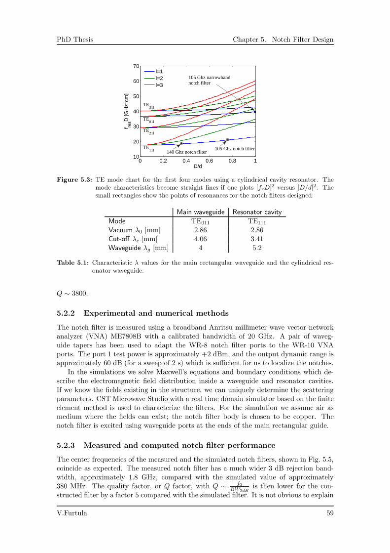
PhD Thesis Chapter 5. Notch Filter Design
0 0.2 0.4 0.6 0.8 110
20
30
40
50
60
70
f resD
[GH
z*cm
]
D/d
l=1l=2l=3
TE31l
140 Ghz notch filter
105 Ghz narrowbandnotch filter
105 Ghz notch filterTE11l
TE21l
TE01l
Figure 5.3: TE mode chart for the first four modes using a cylindrical cavity resonator. Themode characteristics become straight lines if one plots [frD]2 versus [D/d]2. Thesmall rectangles show the points of resonances for the notch filters designed.
Main waveguide Resonator cavity
Mode TE011 TE111
Vacuum λ0 [mm] 2.86 2.86Cut-off λc [mm] 4.06 3.41Waveguide λg [mm] 4 5.2
Table 5.1: Characteristic λ values for the main rectangular waveguide and the cylindrical res-onator waveguide.
Q ∼ 3800.
5.2.2 Experimental and numerical methods
The notch filter is measured using a broadband Anritsu millimeter wave vector networkanalyzer (VNA) ME7808B with a calibrated bandwidth of 20 GHz. A pair of waveg-uide tapers has been used to adapt the WR-8 notch filter ports to the WR-10 VNAports. The port 1 test power is approximately +2 dBm, and the output dynamic range isapproximately 60 dB (for a sweep of 2 s) which is sufficient for us to localize the notches.
In the simulations we solve Maxwell’s equations and boundary conditions which de-scribe the electromagnetic field distribution inside a waveguide and resonator cavities.If we know the fields existing in the structure, we can uniquely determine the scatteringparameters. CST Microwave Studio with a real time domain simulator based on the finiteelement method is used to characterize the filters. For the simulation we assume air asmedium where the fields can exist; the notch filter body is chosen to be copper. Thenotch filter is excited using waveguide ports at the ends of the main rectangular guide.
5.2.3 Measured and computed notch filter performance
The center frequencies of the measured and the simulated notch filters, shown in Fig. 5.5,coincide as expected. The measured notch filter has a much wider 3 dB rejection band-width, approximately 1.8 GHz, compared with the simulated value of approximately380 MHz. The quality factor, or Q factor, with Q ∼ f0
BW3dBis then lower for the con-
structed filter by a factor 5 compared with the simulated filter. It is not obvious to explain
V.Furtula 59
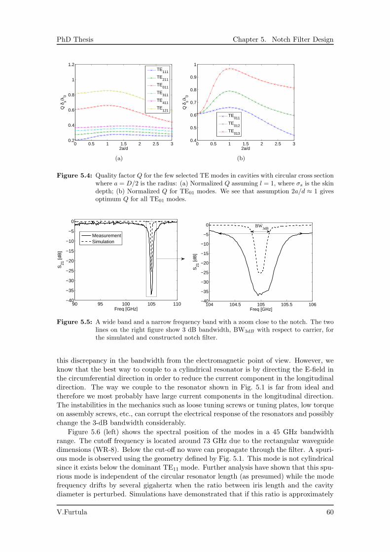
PhD Thesis Chapter 5. Notch Filter Design
0 0.5 1 1.5 2 2.5 30.2
0.4
0.6
0.8
1
1.2
2a/d
Q δ
s/λ0
TE111
TE211
TE011
TE311
TE411
TE121
(a)
0 0.5 1 1.5 2 2.5 30.4
0.5
0.6
0.7
0.8
0.9
1
2a/d
Q δ
s/λ0
TE011
TE012
TE013
(b)
Figure 5.4: Quality factor Q for the few selected TE modes in cavities with circular cross sectionwhere a = D/2 is the radius: (a) Normalized Q assuming l = 1, where σs is the skindepth; (b) Normalized Q for TE01 modes. We see that assumption 2a/d ≈ 1 givesoptimum Q for all TE01 modes.
90 95 100 105 110−40
−35
−30
−25
−20
−15
−10
−5
0
S21
[dB
]
Freq [GHz]
MeasurementSimulation
104 104.5 105 105.5 106−40
−35
−30
−25
−20
−15
−10
−5
0
S21
[dB
]
Freq [GHz]
BW
3dB
Figure 5.5: A wide band and a narrow frequency band with a zoom close to the notch. The twolines on the right figure show 3 dB bandwidth, BW3dB with respect to carrier, forthe simulated and constructed notch filter.
this discrepancy in the bandwidth from the electromagnetic point of view. However, weknow that the best way to couple to a cylindrical resonator is by directing the E-field inthe circumferential direction in order to reduce the current component in the longitudinaldirection. The way we couple to the resonator shown in Fig. 5.1 is far from ideal andtherefore we most probably have large current components in the longitudinal direction.The instabilities in the mechanics such as loose tuning screws or tuning plates, low torqueon assembly screws, etc., can corrupt the electrical response of the resonators and possiblychange the 3-dB bandwidth considerably.
Figure 5.6 (left) shows the spectral position of the modes in a 45 GHz bandwidthrange. The cutoff frequency is located around 73 GHz due to the rectangular waveguidedimensions (WR-8). Below the cut-off no wave can propagate through the filter. A spuri-ous mode is observed using the geometry defined by Fig. 5.1. This mode is not cylindricalsince it exists below the dominant TE11 mode. Further analysis have shown that this spu-rious mode is independent of the circular resonator length (as presumed) while the modefrequency drifts by several gigahertz when the ratio between iris length and the cavitydiameter is perturbed. Simulations have demonstrated that if this ratio is approximately
V.Furtula 60
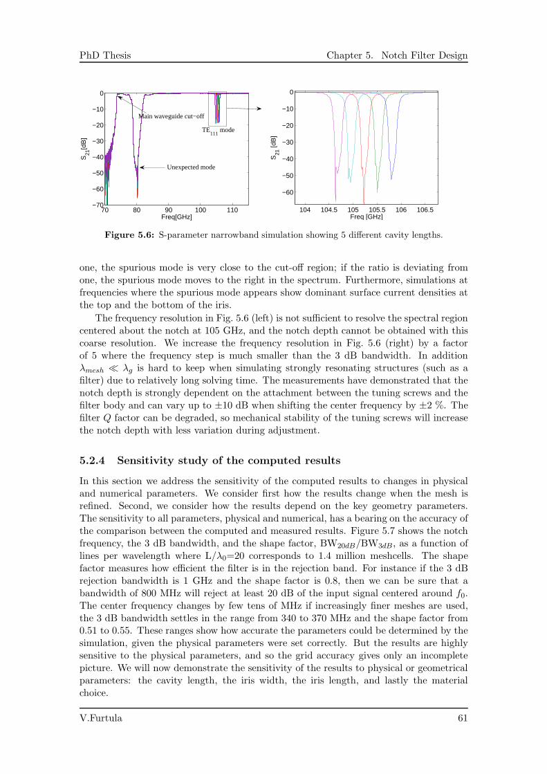
PhD Thesis Chapter 5. Notch Filter Design
70 80 90 100 110−70
−60
−50
−40
−30
−20
−10
0
Freq[GHz]
S21
[dB
]
Main waveguide cut−off
TE111
mode
Unexpected mode
104 104.5 105 105.5 106 106.5
−60
−50
−40
−30
−20
−10
0
Freq [GHz]
S21
[dB
]
Figure 5.6: S-parameter narrowband simulation showing 5 different cavity lengths.
one, the spurious mode is very close to the cut-off region; if the ratio is deviating fromone, the spurious mode moves to the right in the spectrum. Furthermore, simulations atfrequencies where the spurious mode appears show dominant surface current densities atthe top and the bottom of the iris.
The frequency resolution in Fig. 5.6 (left) is not sufficient to resolve the spectral regioncentered about the notch at 105 GHz, and the notch depth cannot be obtained with thiscoarse resolution. We increase the frequency resolution in Fig. 5.6 (right) by a factorof 5 where the frequency step is much smaller than the 3 dB bandwidth. In additionλmesh ≪ λg is hard to keep when simulating strongly resonating structures (such as afilter) due to relatively long solving time. The measurements have demonstrated that thenotch depth is strongly dependent on the attachment between the tuning screws and thefilter body and can vary up to ±10 dB when shifting the center frequency by ±2 %. Thefilter Q factor can be degraded, so mechanical stability of the tuning screws will increasethe notch depth with less variation during adjustment.
5.2.4 Sensitivity study of the computed results
In this section we address the sensitivity of the computed results to changes in physicaland numerical parameters. We consider first how the results change when the mesh isrefined. Second, we consider how the results depend on the key geometry parameters.The sensitivity to all parameters, physical and numerical, has a bearing on the accuracy ofthe comparison between the computed and measured results. Figure 5.7 shows the notchfrequency, the 3 dB bandwidth, and the shape factor, BW20dB/BW3dB , as a function oflines per wavelength where L/λ0=20 corresponds to 1.4 million meshcells. The shapefactor measures how efficient the filter is in the rejection band. For instance if the 3 dBrejection bandwidth is 1 GHz and the shape factor is 0.8, then we can be sure that abandwidth of 800 MHz will reject at least 20 dB of the input signal centered around f0.The center frequency changes by few tens of MHz if increasingly finer meshes are used,the 3 dB bandwidth settles in the range from 340 to 370 MHz and the shape factor from0.51 to 0.55. These ranges show how accurate the parameters could be determined by thesimulation, given the physical parameters were set correctly. But the results are highlysensitive to the physical parameters, and so the grid accuracy gives only an incompletepicture. We will now demonstrate the sensitivity of the results to physical or geometricalparameters: the cavity length, the iris width, the iris length, and lastly the materialchoice.
V.Furtula 61
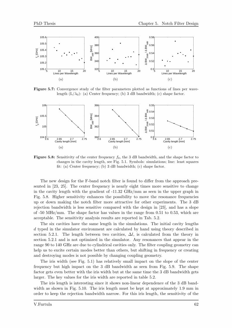
PhD Thesis Chapter 5. Notch Filter Design
5 10 15 20105.1
105.2
105.3
105.4
105.5
105.6
Lines per Wavelength
f 0 [GH
z]
(a)
5 10 15 20320
340
360
380
400
Lines per Wavelength
BW
3dB [M
Hz]
(b)
5 10 15 200.5
0.52
0.54
0.56
0.58
Lines per Wavelength
∆ B
W20
dB /
∆ B
W3d
B
(c)
Figure 5.7: Convergence study of the filter parameters plotted as functions of lines per wave-length (L/λ0): (a) Center frequency; (b) 3 dB bandwidth; (c) shape factor.
2.6 2.65 2.7 2.75104.5
105
105.5
106
Cavity length [mm]
f 0 [GH
z]
(a)
2.6 2.65 2.7 2.75360
362
364
366
Cavity length [mm]
BW
3dB [M
Hz]
(b)
2.6 2.65 2.7 2.750.5
0.51
0.52
0.53
0.54
0.55
Cavity length [mm]
∆ B
W20
dB /
∆ B
W3d
B(c)
Figure 5.8: Sensitivity of the center frequency f0, the 3 dB bandwidth, and the shape factor tochanges in the cavity length, see Fig. 5.1. Symbols: simulations; line: least squaresfit: (a) Center frequency; (b) 3 dB bandwidth; (c) shape factor.
The new design for the F-band notch filter is found to differ from the approach pre-sented in [23, 25]. The center frequency is nearly eight times more sensitive to changein the cavity length with the gradient of -11.32 GHz/mm as seen in the upper graph inFig. 5.8. Higher sensitivity enhances the possibility to move the resonance frequenciesup or down making the notch filter more attractive for other experiments. The 3 dBrejection bandwidth is less sensitive compared with the design in [23], and has a slopeof -50 MHz/mm. The shape factor has values in the range from 0.51 to 0.53, which areacceptable. The sensitivity analysis results are reported in Tab. 5.2.
The six cavities have the same length in the simulations. The initial cavity lengthsd typed in the simulator environment are calculated by hand using theory described insection 5.2.1. The length between two cavities, ∆l, is calculated from the theory insection 5.2.1 and is not optimized in the simulator. Any resonances that appear in therange 90 to 140 GHz are due to cylindrical cavities only. The filter coupling geometry canhelp us to excite certain modes better than others, but shifting in frequency or creatingand destroying modes is not possible by changing coupling geometry.
The iris width (see Fig. 5.1) has relatively small impact on the slope of the centerfrequency but high impact on the 3 dB bandwidth as seen from Fig. 5.9. The shapefactor gets even better with the iris width but at the same time the 3 dB bandwidth getslarger. The key values for the iris width are reported in table 5.2.
The iris length is interesting since it shows non-linear dependence of the 3 dB band-width as shown in Fig. 5.10. The iris length must be kept at approximately 1.9 mm inorder to keep the rejection bandwidth narrow. For this iris length, the sensitivity of the
V.Furtula 62
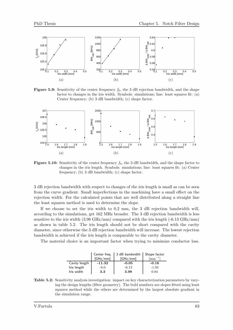
PhD Thesis Chapter 5. Notch Filter Design
0.1 0.2 0.3 0.4 0.5105.2
105.4
105.6
105.8
106
Iris width [mm]
f 0 [GH
z]
(a)
0.1 0.2 0.3 0.4 0.5200
400
600
800
1000
1200
Iris width [mm]
BW
3dB [M
Hz]
(b)
0.1 0.2 0.3 0.4 0.50.54
0.56
0.58
0.6
0.62
0.64
Iris width [mm]
∆ B
W20
dB /
∆ B
W3d
B
(c)
Figure 5.9: Sensitivity of the center frequency f0, the 3 dB rejection bandwidth, and the shapefactor to changes in the iris width. Symbols: simulations; line: least squares fit: (a)Center frequency; (b) 3 dB bandwidth; (c) shape factor.
1.5 1.6 1.7 1.8 1.9104.5
105
105.5
106
106.5
107
Iris length [mm]
f 0 [GH
z]
(a)
1.5 1.6 1.7 1.8 1.90
500
1000
1500
Iris length [mm]
BW
3dB [M
Hz]
(b)
1.5 1.6 1.7 1.8 1.9
0.4
0.5
0.6
0.7
Iris length [mm]∆
BW
20dB
/ ∆
BW
3dB
(c)
Figure 5.10: Sensitivity of the center frequency f0, the 3 dB bandwidth, and the shape factor tochanges in the iris length. Symbols: simulations; line: least squares fit: (a) Centerfrequency; (b) 3 dB bandwidth; (c) shape factor.
3 dB rejection bandwidth with respect to changes of the iris length is small as can be seenfrom the curve gradient. Small imperfections in the machining have a small effect on therejection width. For the calculated points that are well distributed along a straight linethe least squares method is used to determine the slope.
If we choose to set the iris width to 0.2 mm, the 3 dB rejection bandwidth will,according to the simulations, get 162 MHz broader. The 3 dB rejection bandwidth is lesssensitive to the iris width (3.98 GHz/mm) compared with the iris length (-6.13 GHz/mm)as shown in table 5.2. The iris length should not be short compared with the cavitydiameter, since otherwise the 3 dB rejection bandwidth will increase. The lowest rejectionbandwidth is achieved if the iris length is comparable to the cavity diameter.
The material choice is an important factor when trying to minimize conductor loss.
Center freq. 3 dB bandwidth Shape factor[GHz/mm] [GHz/mm] [mm−1]
Cavity length -11.32 -0.05 -0.16
Iris length -8.0 -6.13 -1.93Iris width 3.3 3.98 0.84
Table 5.2: Sensitivity analysis investigation: impact on key characterization parameters by vary-ing the design lengths (filter geometry). The bold numbers are slopes fitted using leastsquares method while the others are determined by the largest absolute gradient inthe simulation range.
V.Furtula 63
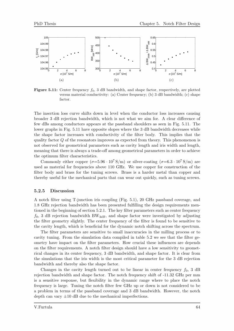
PhD Thesis Chapter 5. Notch Filter Design
0 2 4 6 8104.95
104.96
104.97
104.98
104.99
105
σ [107 S/m]
f 0 [GH
z]
(a)
0 2 4 6 8300
350
400
450
500
σ [107 S/m]
BW
3dB [M
Hz]
(b)
0 2 4 6 80.4
0.45
0.5
0.55
0.6
0.65
σ [107 S/m]
∆ B
W20
dB /
∆ B
W3d
B
(c)
Figure 5.11: Center frequency f0, 3 dB bandwidth, and shape factor, respectively, are plottedversus material conductivity: (a) Center frequency; (b) 3 dB bandwidth; (c) shapefactor.
The insertion loss curve shifts down in level when the conductor loss increases causingbroader 3 dB rejection bandwidth, which is not what we aim for. A clear difference offew dBs among conductors appears at the passband shoulders as seen in Fig. 5.11. Thelower graphs in Fig. 5.11 have opposite slopes where the 3 dB bandwidth decreases whilethe shape factor increases with conductivity of the filter body. This implies that thequality factor Q of the resonators improves as expected from theory. This phenomenon isnot observed for geometrical parameters such as cavity length and iris width and length,meaning that there is always a trade-off among geometrical parameters in order to achievethe optimum filter characteristics.
Commonly either copper (σ=5.96 · 107 S/m) or silver-coating (σ=6.3 · 107 S/m) areused as material for frequencies above 110 GHz. We use copper for construction of thefilter body and brass for the tuning screws. Brass is a harder metal than copper andthereby useful for the mechanical parts that can wear out quickly, such as tuning screws.
5.2.5 Discussion
A notch filter using T-junction iris coupling (Fig. 5.1), 20 GHz passband coverage, and1.8 GHz rejection bandwidth has been presented fulfilling the design requirements men-tioned in the beginning of section 5.2.1. The key filter parameters such as center frequencyf0, 3 dB rejection bandwidth BW3dB , and shape factor were investigated by adjustingthe filter geometry slightly. The center frequency of the filter is found to be sensitive tothe cavity length, which is beneficial for the dynamic notch shifting across the spectrum.
The filter parameters are sensitive to small inaccuracies in the milling process or tocavity tuning. From the simulation data compiled in table 5.2 we see that the filter ge-ometry have impact on the filter parameters. How crucial these influences are dependson the filter requirements. A notch filter design should have a low sensitivity to geomet-rical changes in its center frequency, 3 dB bandwidth, and shape factor. It is clear fromthe simulations that the iris width is the most critical parameter for the 3 dB rejectionbandwidth and thereby also the shape factor.
Changes in the cavity length turned out to be linear in center frequency f0, 3 dBrejection bandwidth and shape factor. The notch frequency shift of -11.32 GHz per mmis a sensitive response, but flexibility in the dynamic range where to place the notchfrequency is large. Tuning the notch filter few GHz up or down is not considered to bea problem in terms of the passband coverage and 3 dB bandwidth. However, the notchdepth can vary ±10 dB due to the mechanical imperfections.
V.Furtula 64
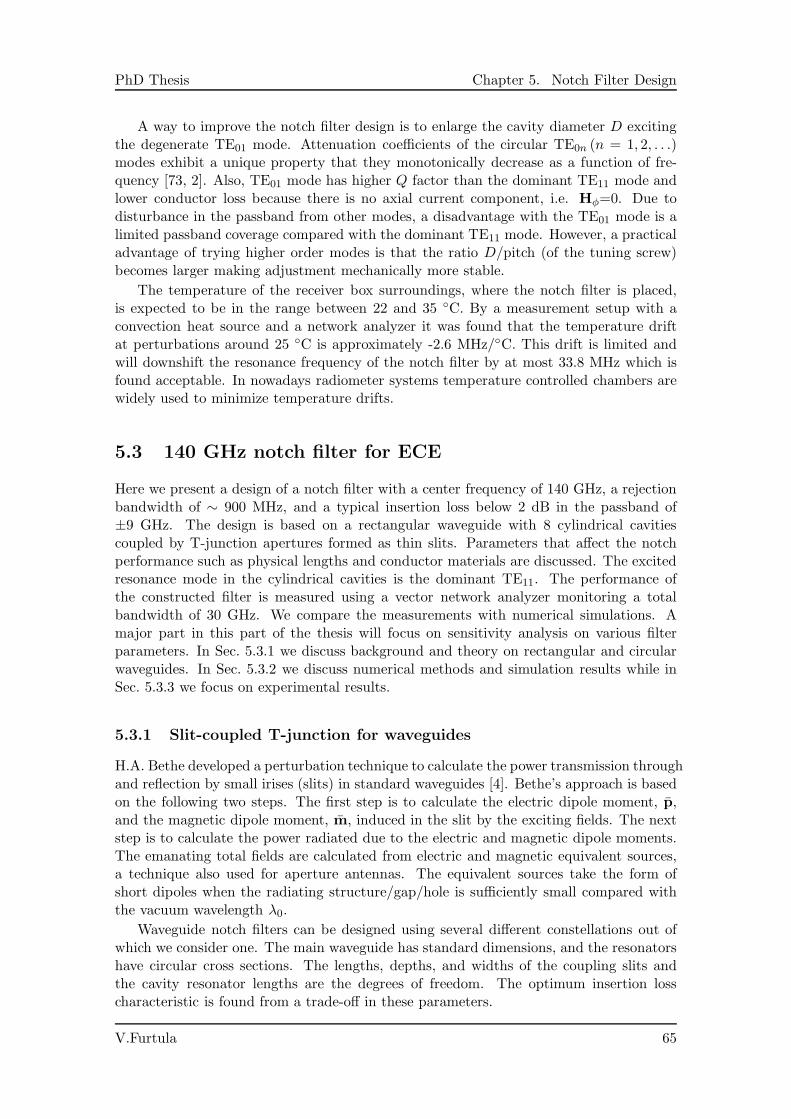
PhD Thesis Chapter 5. Notch Filter Design
A way to improve the notch filter design is to enlarge the cavity diameter D excitingthe degenerate TE01 mode. Attenuation coefficients of the circular TE0n (n = 1, 2, . . .)modes exhibit a unique property that they monotonically decrease as a function of fre-quency [73, 2]. Also, TE01 mode has higher Q factor than the dominant TE11 mode andlower conductor loss because there is no axial current component, i.e. Hφ=0. Due todisturbance in the passband from other modes, a disadvantage with the TE01 mode is alimited passband coverage compared with the dominant TE11 mode. However, a practicaladvantage of trying higher order modes is that the ratio D/pitch (of the tuning screw)becomes larger making adjustment mechanically more stable.
The temperature of the receiver box surroundings, where the notch filter is placed,is expected to be in the range between 22 and 35 C. By a measurement setup with aconvection heat source and a network analyzer it was found that the temperature driftat perturbations around 25 C is approximately -2.6 MHz/C. This drift is limited andwill downshift the resonance frequency of the notch filter by at most 33.8 MHz which isfound acceptable. In nowadays radiometer systems temperature controlled chambers arewidely used to minimize temperature drifts.
5.3 140 GHz notch filter for ECE
Here we present a design of a notch filter with a center frequency of 140 GHz, a rejectionbandwidth of ∼ 900 MHz, and a typical insertion loss below 2 dB in the passband of±9 GHz. The design is based on a rectangular waveguide with 8 cylindrical cavitiescoupled by T-junction apertures formed as thin slits. Parameters that affect the notchperformance such as physical lengths and conductor materials are discussed. The excitedresonance mode in the cylindrical cavities is the dominant TE11. The performance ofthe constructed filter is measured using a vector network analyzer monitoring a totalbandwidth of 30 GHz. We compare the measurements with numerical simulations. Amajor part in this part of the thesis will focus on sensitivity analysis on various filterparameters. In Sec. 5.3.1 we discuss background and theory on rectangular and circularwaveguides. In Sec. 5.3.2 we discuss numerical methods and simulation results while inSec. 5.3.3 we focus on experimental results.
5.3.1 Slit-coupled T-junction for waveguides
H.A. Bethe developed a perturbation technique to calculate the power transmission throughand reflection by small irises (slits) in standard waveguides [4]. Bethe’s approach is basedon the following two steps. The first step is to calculate the electric dipole moment, p,and the magnetic dipole moment, m, induced in the slit by the exciting fields. The nextstep is to calculate the power radiated due to the electric and magnetic dipole moments.The emanating total fields are calculated from electric and magnetic equivalent sources,a technique also used for aperture antennas. The equivalent sources take the form ofshort dipoles when the radiating structure/gap/hole is sufficiently small compared withthe vacuum wavelength λ0.
Waveguide notch filters can be designed using several different constellations out ofwhich we consider one. The main waveguide has standard dimensions, and the resonatorshave circular cross sections. The lengths, depths, and widths of the coupling slits andthe cavity resonator lengths are the degrees of freedom. The optimum insertion losscharacteristic is found from a trade-off in these parameters.
V.Furtula 65
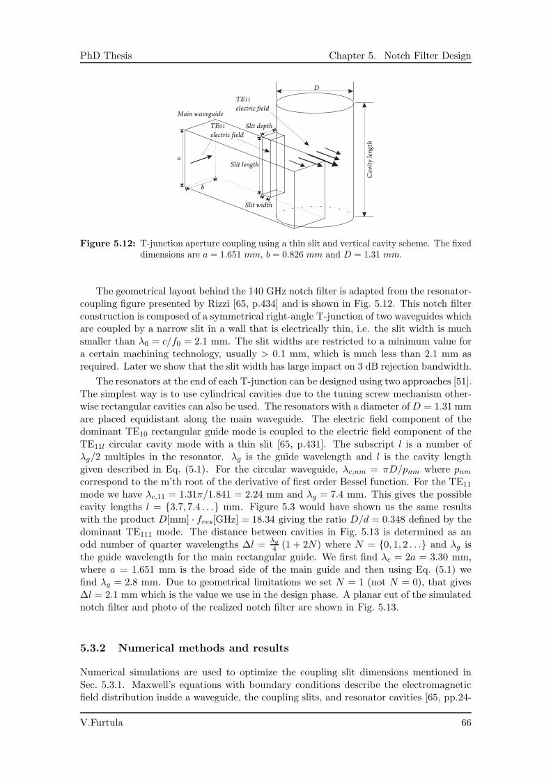
PhD Thesis Chapter 5. Notch Filter Design
D
Main waveguide
TE
electric field
11
TE
electric field
01 Slit depth
Slit length
Slit width
a
b
Ca
vity
len
gth
Figure 5.12: T-junction aperture coupling using a thin slit and vertical cavity scheme. The fixeddimensions are a = 1.651 mm, b = 0.826 mm and D = 1.31 mm.
The geometrical layout behind the 140 GHz notch filter is adapted from the resonator-coupling figure presented by Rizzi [65, p.434] and is shown in Fig. 5.12. This notch filterconstruction is composed of a symmetrical right-angle T-junction of two waveguides whichare coupled by a narrow slit in a wall that is electrically thin, i.e. the slit width is muchsmaller than λ0 = c/f0 = 2.1 mm. The slit widths are restricted to a minimum value fora certain machining technology, usually > 0.1 mm, which is much less than 2.1 mm asrequired. Later we show that the slit width has large impact on 3 dB rejection bandwidth.
The resonators at the end of each T-junction can be designed using two approaches [51].The simplest way is to use cylindrical cavities due to the tuning screw mechanism other-wise rectangular cavities can also be used. The resonators with a diameter ofD = 1.31 mmare placed equidistant along the main waveguide. The electric field component of thedominant TE10 rectangular guide mode is coupled to the electric field component of theTE11l circular cavity mode with a thin slit [65, p.431]. The subscript l is a number ofλg/2 multiples in the resonator. λg is the guide wavelength and l is the cavity lengthgiven described in Eq. (5.1). For the circular waveguide, λc,nm = πD/pnm where pnmcorrespond to the m’th root of the derivative of first order Bessel function. For the TE11
mode we have λc,11 = 1.31π/1.841 = 2.24 mm and λg = 7.4 mm. This gives the possiblecavity lengths l = 3.7, 7.4 . . . mm. Figure 5.3 would have shown us the same resultswith the product D[mm] · fres[GHz] = 18.34 giving the ratio D/d = 0.348 defined by thedominant TE111 mode. The distance between cavities in Fig. 5.13 is determined as anodd number of quarter wavelengths ∆l =
λg
4 (1 + 2N) where N = 0, 1, 2 . . . and λg isthe guide wavelength for the main rectangular guide. We first find λc = 2a = 3.30 mm,where a = 1.651 mm is the broad side of the main guide and then using Eq. (5.1) wefind λg = 2.8 mm. Due to geometrical limitations we set N = 1 (not N = 0), that gives∆l = 2.1 mm which is the value we use in the design phase. A planar cut of the simulatednotch filter and photo of the realized notch filter are shown in Fig. 5.13.
5.3.2 Numerical methods and results
Numerical simulations are used to optimize the coupling slit dimensions mentioned inSec. 5.3.1. Maxwell’s equations with boundary conditions describe the electromagneticfield distribution inside a waveguide, the coupling slits, and resonator cavities [65, pp.24-
V.Furtula 66
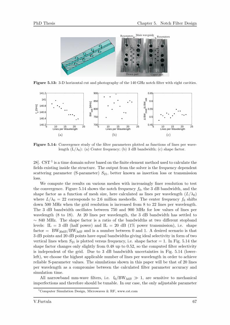
PhD Thesis Chapter 5. Notch Filter Design
Upper partDown part
Main wavguideResonators Resonators
Figure 5.13: 3-D horizontal cut and photography of the 140 GHz notch filter with eight cavities.
5 10 15 20 25140.2
140.4
140.6
140.8
141
141.2
Lines per Wavelength
f 0 [GH
z]
(a)
5 10 15 20 25700
750
800
850
900
Lines per Wavelength
BW
3dB [M
Hz]
(b)
5 10 15 20 250.45
0.5
0.55
0.6
0.65
Lines per Wavelength
∆ B
W20
dB/∆
BW
3dB
(c)
Figure 5.14: Convergence study of the filter parameters plotted as functions of lines per wave-length (L/λ0): (a) Center frequency; (b) 3 dB bandwidth; (c) shape factor.
28]. CST 1 is a time domain solver based on the finite element method used to calculate thefields existing inside the structure. The output from the solver is the frequency dependentscattering parameter (S-parameter) S21, better known as insertion loss or transmissionloss.
We compute the results on various meshes with increasingly finer resolution to testthe convergence. Figure 5.14 shows the notch frequency f0, the 3 dB bandwidth, and theshape factor as a function of mesh size, here calculated as lines per wavelength (L/λ0)where L/λ0 = 22 corresponds to 2.6 million meshcells. The center frequency f0 shiftsdown 500 MHz when the grid resolution is increased from 8 to 22 lines per wavelength.The 3 dB bandwidth oscillates between 750 and 900 MHz for low values of lines perwavelength (8 to 18). At 20 lines per wavelength, the 3 dB bandwidth has settled to∼ 840 MHz. The shape factor is a ratio of the bandwidths at two different stopbandlevels: IL = 3 dB (half power) and IL = 20 dB (1% power transmission), i.e. shapefactor = BW20dB/BW3dB and is a number between 0 and 1. A desired scenario is that3 dB points and 20 dB points have equal bandwidths giving ideal selectivity in form of twovertical lines when S21 is plotted versus frequency, i.e. shape factor = 1. In Fig. 5.14 theshape factor changes only slightly from 0.48 up to 0.52, so the computed filter selectivityis independent of the grid. Due to 3 dB bandwidth uncertainties in Fig. 5.14 (lower-left), we choose the highest applicable number of lines per wavelength in order to achievereliable S-parameter values. The simulations shown in this paper will be that of 20 linesper wavelength as a compromise between the calculated filter parameter accuracy andsimulation time.
All narrowband mm-wave filters, i.e. f0/BW3dB ≫ 1, are sensitive to mechanicalimperfections and therefore should be tunable. In our case, the only adjustable parameter
1Computer Simulation Design, Microwaves & RF, www.cst.com
V.Furtula 67
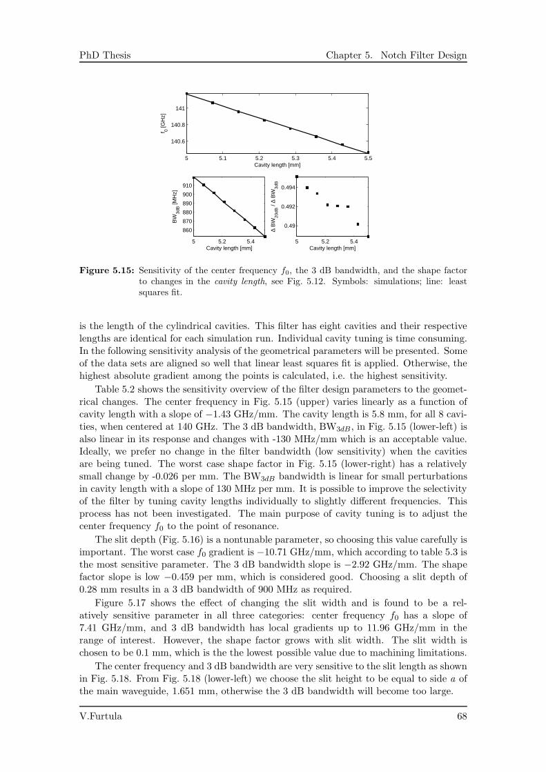
PhD Thesis Chapter 5. Notch Filter Design
5 5.1 5.2 5.3 5.4 5.5
140.6
140.8
141
Cavity length [mm]f 0 [G
Hz]
5 5.2 5.4
860
870
880
890
900
910
Cavity length [mm]
BW
3dB [M
Hz]
5 5.2 5.4
0.49
0.492
0.494
Cavity length [mm]
∆ B
W20
dB /
∆ B
W3d
BFigure 5.15: Sensitivity of the center frequency f0, the 3 dB bandwidth, and the shape factor
to changes in the cavity length, see Fig. 5.12. Symbols: simulations; line: leastsquares fit.
is the length of the cylindrical cavities. This filter has eight cavities and their respectivelengths are identical for each simulation run. Individual cavity tuning is time consuming.In the following sensitivity analysis of the geometrical parameters will be presented. Someof the data sets are aligned so well that linear least squares fit is applied. Otherwise, thehighest absolute gradient among the points is calculated, i.e. the highest sensitivity.
Table 5.2 shows the sensitivity overview of the filter design parameters to the geomet-rical changes. The center frequency in Fig. 5.15 (upper) varies linearly as a function ofcavity length with a slope of −1.43 GHz/mm. The cavity length is 5.8 mm, for all 8 cavi-ties, when centered at 140 GHz. The 3 dB bandwidth, BW3dB , in Fig. 5.15 (lower-left) isalso linear in its response and changes with -130 MHz/mm which is an acceptable value.Ideally, we prefer no change in the filter bandwidth (low sensitivity) when the cavitiesare being tuned. The worst case shape factor in Fig. 5.15 (lower-right) has a relativelysmall change by -0.026 per mm. The BW3dB bandwidth is linear for small perturbationsin cavity length with a slope of 130 MHz per mm. It is possible to improve the selectivityof the filter by tuning cavity lengths individually to slightly different frequencies. Thisprocess has not been investigated. The main purpose of cavity tuning is to adjust thecenter frequency f0 to the point of resonance.
The slit depth (Fig. 5.16) is a nontunable parameter, so choosing this value carefully isimportant. The worst case f0 gradient is −10.71 GHz/mm, which according to table 5.3 isthe most sensitive parameter. The 3 dB bandwidth slope is −2.92 GHz/mm. The shapefactor slope is low −0.459 per mm, which is considered good. Choosing a slit depth of0.28 mm results in a 3 dB bandwidth of 900 MHz as required.
Figure 5.17 shows the effect of changing the slit width and is found to be a rel-atively sensitive parameter in all three categories: center frequency f0 has a slope of7.41 GHz/mm, and 3 dB bandwidth has local gradients up to 11.96 GHz/mm in therange of interest. However, the shape factor grows with slit width. The slit width ischosen to be 0.1 mm, which is the the lowest possible value due to machining limitations.
The center frequency and 3 dB bandwidth are very sensitive to the slit length as shownin Fig. 5.18. From Fig. 5.18 (lower-left) we choose the slit height to be equal to side a ofthe main waveguide, 1.651 mm, otherwise the 3 dB bandwidth will become too large.
V.Furtula 68
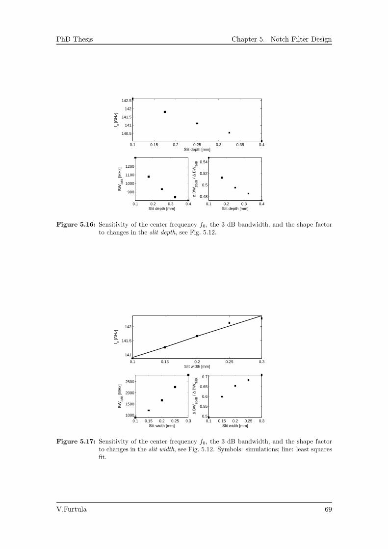
PhD Thesis Chapter 5. Notch Filter Design
0.1 0.15 0.2 0.25 0.3 0.35 0.4
140.5
141
141.5
142
142.5
Slit depth [mm]
f 0 [GH
z]
0.1 0.2 0.3 0.4
900
1000
1100
1200
Slit depth [mm]
BW
3dB [M
Hz]
0.1 0.2 0.3 0.4
0.48
0.5
0.52
0.54
Slit depth [mm]
∆ B
W20
dB /
∆ B
W3d
B
Figure 5.16: Sensitivity of the center frequency f0, the 3 dB bandwidth, and the shape factorto changes in the slit depth, see Fig. 5.12.
0.1 0.15 0.2 0.25 0.3
141
141.5
142
Slit width [mm]
f 0 [GH
z]
0.1 0.15 0.2 0.25 0.31000
1500
2000
2500
Slit width [mm]
BW
3dB [M
Hz]
0.1 0.15 0.2 0.25 0.30.5
0.55
0.6
0.65
0.7
Slit width [mm]
∆ B
W20
dB /
∆ B
W3d
B
Figure 5.17: Sensitivity of the center frequency f0, the 3 dB bandwidth, and the shape factorto changes in the slit width, see Fig. 5.12. Symbols: simulations; line: least squaresfit.
V.Furtula 69
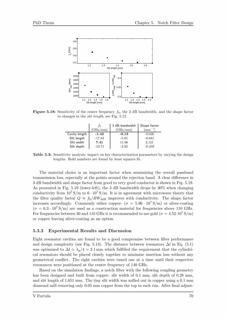
PhD Thesis Chapter 5. Notch Filter Design
1.2 1.3 1.4 1.5 1.6141
142
143
144
Slit length [mm]f 0 [G
Hz]
1.2 1.3 1.4 1.5 1.6
1000
1200
1400
1600
1800
2000
Slit length [mm]
BW
3dB [M
Hz]
1.2 1.3 1.4 1.5 1.60.5
0.55
0.6
Slit length [mm]
∆ B
W20
dB /
∆ B
W3d
BFigure 5.18: Sensitivity of the center frequency f0, the 3 dB bandwidth, and the shape factor
to changes in the slit length, see Fig. 5.12.
f0 3 dB bandwidth Shape factor[GHz/mm] [GHz/mm] [mm−1]
Cavity length -1.43 -0.13 -0.026Slit length -17.83 -5.85 -0.681Slit width 7.41 11.96 2.121Slit depth -10.71 -2.92 -0.459
Table 5.3: Sensitivity analysis: impact on key characterization parameters by varying the designlengths. Bold numbers are found by least squares fit.
The material choice is an important factor when minimizing the overall passbandtransmission loss, especially at the points around the rejection band. A clear difference in3 dB bandwidth and shape factor from good to very good conductor is shown in Fig. 5.19.As presented in Fig. 5.19 (lower-left), the 3 dB bandwidth drops by 30% when changingconductivity from 107 S/m to 6 · 107 S/m. It is in agreement with microwave theory thatthe filter quality factor Q ≈ f0/BW3dB improves with conductivity. The shape factorincreases accordingly. Commonly either copper- (σ = 5.96 · 107 S/m) or silver-coating(σ = 6.3 · 107 S/m) are used as a construction material for frequencies above 110 GHz.For frequencies between 30 and 110 GHz it is recommended to use gold (σ = 4.52·107 S/m)or copper leaving silver-coating as an option.
5.3.3 Experimental Results and Discussion
Eight resonator cavities are found to be a good compromise between filter performanceand design complexity (see Fig. 5.13). The distance between resonators ∆l in Eq. (5.1)was optimized to ∆l ≃ λg/4 ≃ 2.1mm which fulfilled the requirement that the cylindri-cal resonators should be placed closely together to minimize insertion loss without anygeometrical conflict. The eight cavities were tuned one at a time until their respectiveresonances were positioned at the center frequency of 140 GHz.
Based on the simulation findings, a notch filter with the following coupling geometryhas been designed and built from copper: slit width of 0.1 mm, slit depth of 0.28 mm,and slit length of 1.651 mm. The tiny slit width was milled out in copper using a 0.1 mmdiamond mill removing only 0.05 mm copper from the top in each run. After final adjust-
V.Furtula 70
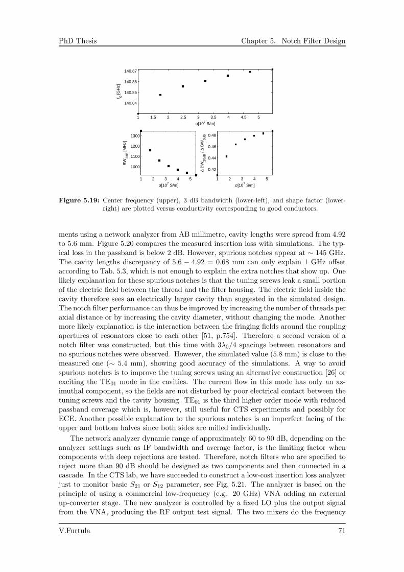
PhD Thesis Chapter 5. Notch Filter Design
1 1.5 2 2.5 3 3.5 4 4.5 5
140.84
140.85
140.86
140.87
σ[107 S/m]f 0 [G
Hz]
1 2 3 4 5
1000
1100
1200
1300
σ[107 S/m]
BW
3dB [M
Hz]
1 2 3 4 5
0.42
0.44
0.46
0.48
σ[107 S/m]
∆ B
W20
dB /
∆ B
W3d
BFigure 5.19: Center frequency (upper), 3 dB bandwidth (lower-left), and shape factor (lower-
right) are plotted versus conductivity corresponding to good conductors.
ments using a network analyzer from AB millimetre, cavity lengths were spread from 4.92to 5.6 mm. Figure 5.20 compares the measured insertion loss with simulations. The typ-ical loss in the passband is below 2 dB. However, spurious notches appear at ∼ 145 GHz.The cavity lengths discrepancy of 5.6 − 4.92 = 0.68 mm can only explain 1 GHz offsetaccording to Tab. 5.3, which is not enough to explain the extra notches that show up. Onelikely explanation for these spurious notches is that the tuning screws leak a small portionof the electric field between the thread and the filter housing. The electric field inside thecavity therefore sees an electrically larger cavity than suggested in the simulated design.The notch filter performance can thus be improved by increasing the number of threads peraxial distance or by increasing the cavity diameter, without changing the mode. Anothermore likely explanation is the interaction between the fringing fields around the couplingapertures of resonators close to each other [51, p.754]. Therefore a second version of anotch filter was constructed, but this time with 3λ0/4 spacings between resonators andno spurious notches were observed. However, the simulated value (5.8 mm) is close to themeasured one (∼ 5.4 mm), showing good accuracy of the simulations. A way to avoidspurious notches is to improve the tuning screws using an alternative construction [26] orexciting the TE01 mode in the cavities. The current flow in this mode has only an az-imuthal component, so the fields are not disturbed by poor electrical contact between thetuning screws and the cavity housing. TE01 is the third higher order mode with reducedpassband coverage which is, however, still useful for CTS experiments and possibly forECE. Another possible explanation to the spurious notches is an imperfect facing of theupper and bottom halves since both sides are milled individually.
The network analyzer dynamic range of approximately 60 to 90 dB, depending on theanalyzer settings such as IF bandwidth and average factor, is the limiting factor whencomponents with deep rejections are tested. Therefore, notch filters who are specified toreject more than 90 dB should be designed as two components and then connected in acascade. In the CTS lab, we have succeeded to construct a low-cost insertion loss analyzerjust to monitor basic S21 or S12 parameter, see Fig. 5.21. The analyzer is based on theprinciple of using a commercial low-frequency (e.g. 20 GHz) VNA adding an externalup-converter stage. The new analyzer is controlled by a fixed LO plus the output signalfrom the VNA, producing the RF output test signal. The two mixers do the frequency
V.Furtula 71
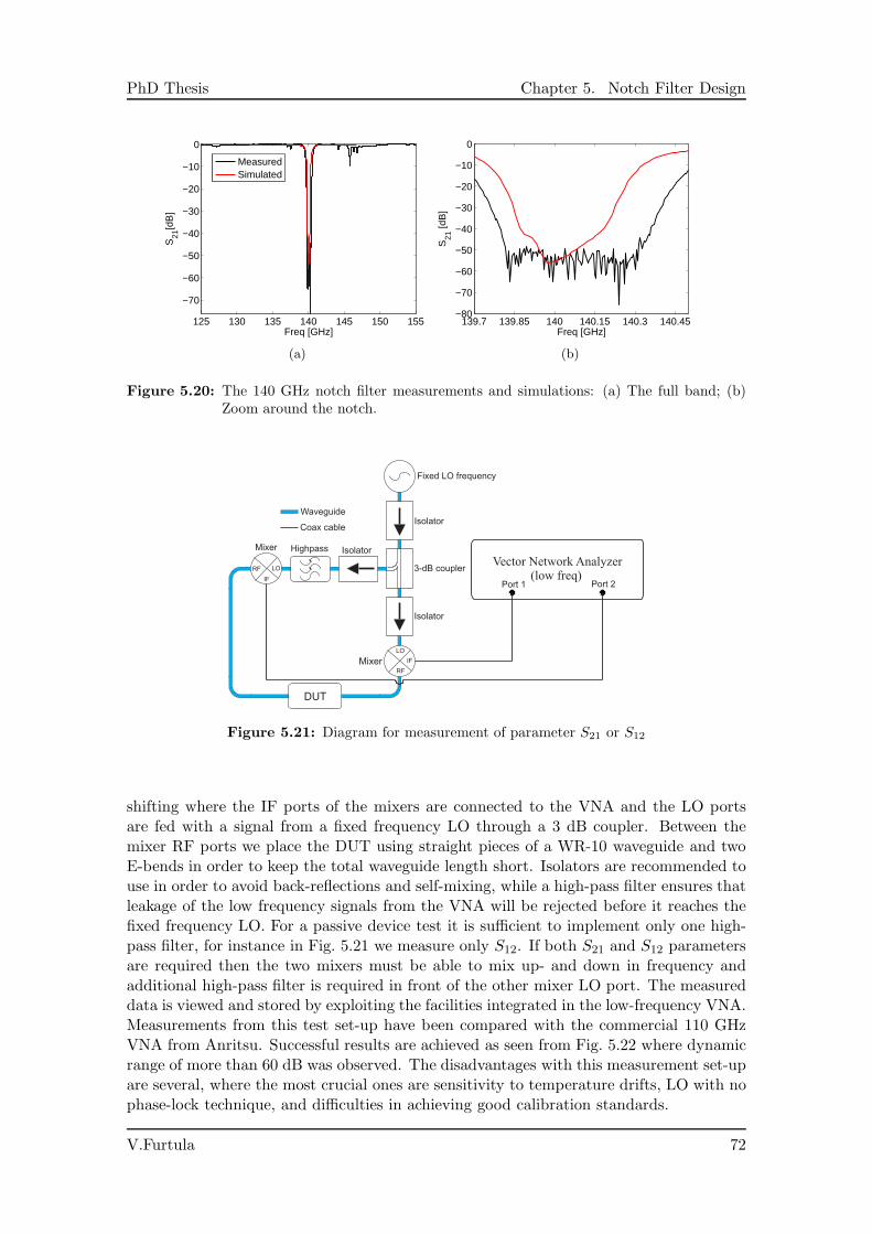
PhD Thesis Chapter 5. Notch Filter Design
125 130 135 140 145 150 155
−70
−60
−50
−40
−30
−20
−10
0
S21
[dB
]
Freq [GHz]
MeasuredSimulated
(a)
139.7 139.85 140 140.15 140.3 140.45−80
−70
−60
−50
−40
−30
−20
−10
0
S21
[dB
]
Freq [GHz]
(b)
Figure 5.20: The 140 GHz notch filter measurements and simulations: (a) The full band; (b)Zoom around the notch.
Fixed LO frequency
Mixer
IF
LORF
IF
LO
RF
Highpass
Vector Network Analyzer(low freq)
Isolator
3-dB coupler
Mixer
Isolator
Isolator
Port 1 Port 2
DUT
Coax cable
Waveguide
Figure 5.21: Diagram for measurement of parameter S21 or S12
shifting where the IF ports of the mixers are connected to the VNA and the LO portsare fed with a signal from a fixed frequency LO through a 3 dB coupler. Between themixer RF ports we place the DUT using straight pieces of a WR-10 waveguide and twoE-bends in order to keep the total waveguide length short. Isolators are recommended touse in order to avoid back-reflections and self-mixing, while a high-pass filter ensures thatleakage of the low frequency signals from the VNA will be rejected before it reaches thefixed frequency LO. For a passive device test it is sufficient to implement only one high-pass filter, for instance in Fig. 5.21 we measure only S12. If both S21 and S12 parametersare required then the two mixers must be able to mix up- and down in frequency andadditional high-pass filter is required in front of the other mixer LO port. The measureddata is viewed and stored by exploiting the facilities integrated in the low-frequency VNA.Measurements from this test set-up have been compared with the commercial 110 GHzVNA from Anritsu. Successful results are achieved as seen from Fig. 5.22 where dynamicrange of more than 60 dB was observed. The disadvantages with this measurement set-upare several, where the most crucial ones are sensitivity to temperature drifts, LO with nophase-lock technique, and difficulties in achieving good calibration standards.
V.Furtula 72
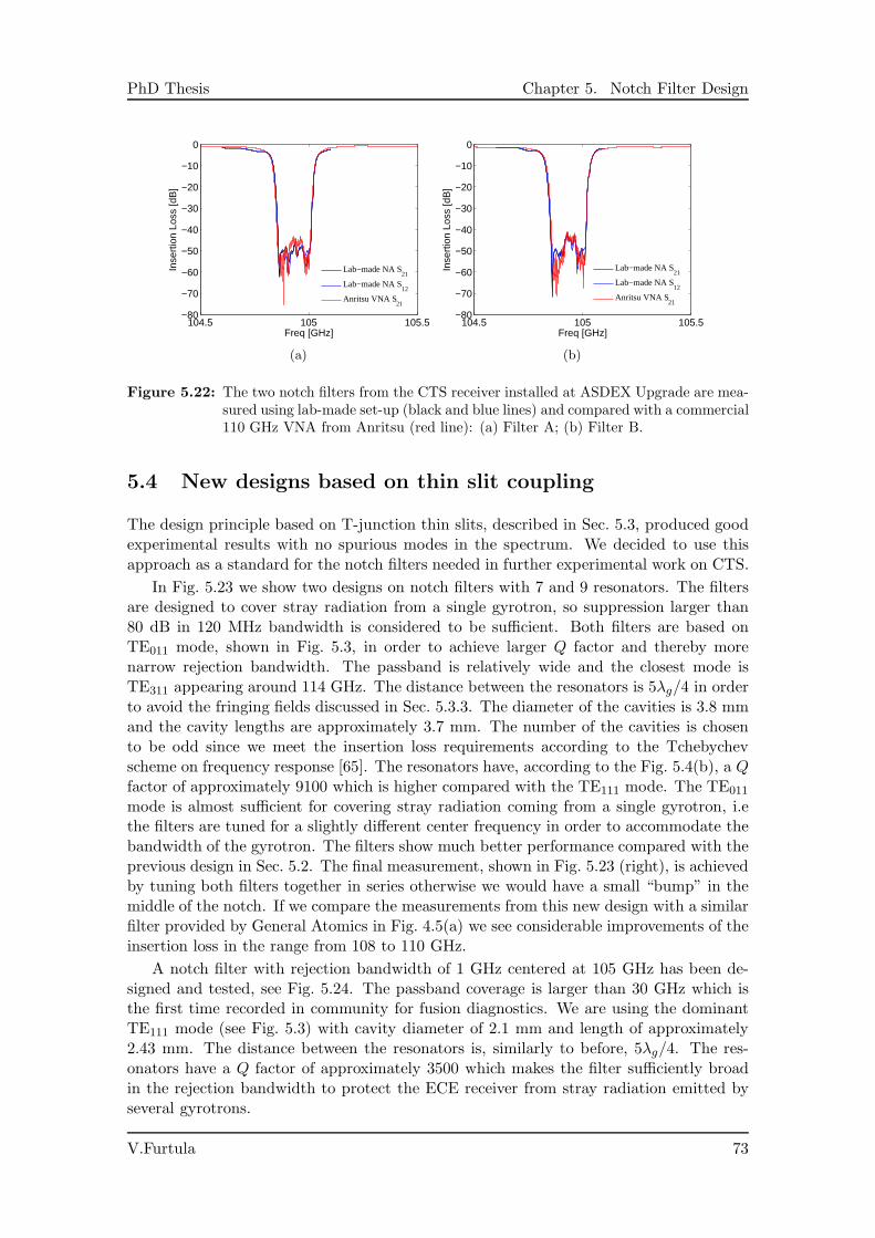
PhD Thesis Chapter 5. Notch Filter Design
104.5 105 105.5−80
−70
−60
−50
−40
−30
−20
−10
0
Inse
rtio
n Lo
ss [d
B]
Freq [GHz]
Lab−made NA S21
Lab−made NA S12
Anritsu VNA S21
(a)
104.5 105 105.5−80
−70
−60
−50
−40
−30
−20
−10
0
Inse
rtio
n Lo
ss [d
B]
Freq [GHz]
Lab−made NA S21
Lab−made NA S12
Anritsu VNA S21
(b)
Figure 5.22: The two notch filters from the CTS receiver installed at ASDEX Upgrade are mea-sured using lab-made set-up (black and blue lines) and compared with a commercial110 GHz VNA from Anritsu (red line): (a) Filter A; (b) Filter B.
5.4 New designs based on thin slit coupling
The design principle based on T-junction thin slits, described in Sec. 5.3, produced goodexperimental results with no spurious modes in the spectrum. We decided to use thisapproach as a standard for the notch filters needed in further experimental work on CTS.
In Fig. 5.23 we show two designs on notch filters with 7 and 9 resonators. The filtersare designed to cover stray radiation from a single gyrotron, so suppression larger than80 dB in 120 MHz bandwidth is considered to be sufficient. Both filters are based onTE011 mode, shown in Fig. 5.3, in order to achieve larger Q factor and thereby morenarrow rejection bandwidth. The passband is relatively wide and the closest mode isTE311 appearing around 114 GHz. The distance between the resonators is 5λg/4 in orderto avoid the fringing fields discussed in Sec. 5.3.3. The diameter of the cavities is 3.8 mmand the cavity lengths are approximately 3.7 mm. The number of the cavities is chosento be odd since we meet the insertion loss requirements according to the Tchebychevscheme on frequency response [65]. The resonators have, according to the Fig. 5.4(b), a Qfactor of approximately 9100 which is higher compared with the TE111 mode. The TE011
mode is almost sufficient for covering stray radiation coming from a single gyrotron, i.ethe filters are tuned for a slightly different center frequency in order to accommodate thebandwidth of the gyrotron. The filters show much better performance compared with theprevious design in Sec. 5.2. The final measurement, shown in Fig. 5.23 (right), is achievedby tuning both filters together in series otherwise we would have a small “bump” in themiddle of the notch. If we compare the measurements from this new design with a similarfilter provided by General Atomics in Fig. 4.5(a) we see considerable improvements of theinsertion loss in the range from 108 to 110 GHz.
A notch filter with rejection bandwidth of 1 GHz centered at 105 GHz has been de-signed and tested, see Fig. 5.24. The passband coverage is larger than 30 GHz which isthe first time recorded in community for fusion diagnostics. We are using the dominantTE111 mode (see Fig. 5.3) with cavity diameter of 2.1 mm and length of approximately2.43 mm. The distance between the resonators is, similarly to before, 5λg/4. The res-onators have a Q factor of approximately 3500 which makes the filter sufficiently broadin the rejection bandwidth to protect the ECE receiver from stray radiation emitted byseveral gyrotrons.
V.Furtula 73
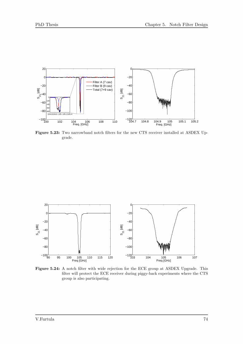
PhD Thesis Chapter 5. Notch Filter Design
100 102 104 106 108 110−100
−80
−60
−40
−20
0
20
Freq. [GHz]
S21
[dB
]
Filter A (7 cav)Filter B (9 cav)Total (7+9 cav)
104.6104.8 105 105.2105.4−80
−60
−40
−20
0
104.7 104.8 104.9 105 105.1 105.2−120
−100
−80
−60
−40
−20
0
Freq. [GHz]S
21 [d
B]
Figure 5.23: Two narrowband notch filters for the new CTS receiver installed at ASDEX Up-grade.
90 95 100 105 110 115 120−100
−80
−60
−40
−20
0
20
S21
[dB
]
Freq [GHz]103 104 105 106 107
−120
−100
−80
−60
−40
−20
0
S21
[dB
]
Freq [GHz]
Figure 5.24: A notch filter with wide rejection for the ECE group at ASDEX Upgrade. Thisfilter will protect the ECE receiver during piggy-back experiments where the CTSgroup is also participating.
V.Furtula 74
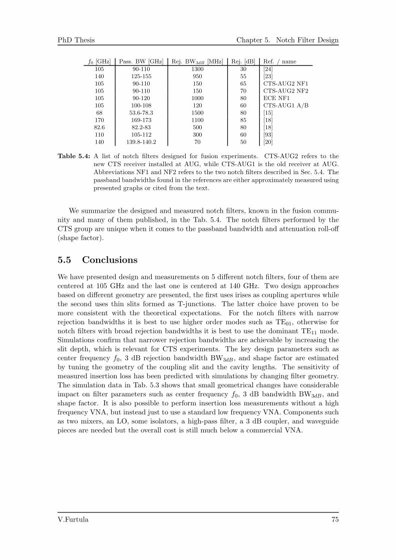
PhD Thesis Chapter 5. Notch Filter Design
f0 [GHz] Pass. BW [GHz] Rej. BW3dB [MHz] Rej. [dB] Ref. / name
105 90-110 1300 30 [24]140 125-155 950 55 [23]105 90-110 150 65 CTS-AUG2 NF1105 90-110 150 70 CTS-AUG2 NF2105 90-120 1000 80 ECE NF1105 100-108 120 60 CTS-AUG1 A/B68 53.6-78.3 1500 80 [15]170 169-173 1100 85 [18]82.6 82.2-83 500 80 [18]110 105-112 300 60 [93]140 139.8-140.2 70 50 [20]
Table 5.4: A list of notch filters designed for fusion experiments. CTS-AUG2 refers to thenew CTS receiver installed at AUG, while CTS-AUG1 is the old receiver at AUG.Abbreviations NF1 and NF2 refers to the two notch filters described in Sec. 5.4. Thepassband bandwidths found in the references are either approximately measured usingpresented graphs or cited from the text.
We summarize the designed and measured notch filters, known in the fusion commu-nity and many of them published, in the Tab. 5.4. The notch filters performed by theCTS group are unique when it comes to the passband bandwidth and attenuation roll-off(shape factor).
5.5 Conclusions
We have presented design and measurements on 5 different notch filters, four of them arecentered at 105 GHz and the last one is centered at 140 GHz. Two design approachesbased on different geometry are presented, the first uses irises as coupling apertures whilethe second uses thin slits formed as T-junctions. The latter choice have proven to bemore consistent with the theoretical expectations. For the notch filters with narrowrejection bandwidths it is best to use higher order modes such as TE01, otherwise fornotch filters with broad rejection bandwidths it is best to use the dominant TE11 mode.Simulations confirm that narrower rejection bandwidths are achievable by increasing theslit depth, which is relevant for CTS experiments. The key design parameters such ascenter frequency f0, 3 dB rejection bandwidth BW3dB , and shape factor are estimatedby tuning the geometry of the coupling slit and the cavity lengths. The sensitivity ofmeasured insertion loss has been predicted with simulations by changing filter geometry.The simulation data in Tab. 5.3 shows that small geometrical changes have considerableimpact on filter parameters such as center frequency f0, 3 dB bandwidth BW3dB , andshape factor. It is also possible to perform insertion loss measurements without a highfrequency VNA, but instead just to use a standard low frequency VNA. Components suchas two mixers, an LO, some isolators, a high-pass filter, a 3 dB coupler, and waveguidepieces are needed but the overall cost is still much below a commercial VNA.
V.Furtula 75

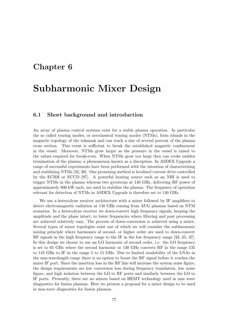
Chapter 6
Subharmonic Mixer Design
6.1 Short background and introduction
An array of plasma control systems exist for a stable plasma operation. In particularthe so called tearing modes, or neoclassical tearing modes (NTMs), form islands in themagnetic topology of the tokamak and can reach a size of several percent of the plasmacross section. This event is sufficient to break the established magnetic confinementin the vessel. Moreover, NTMs grow larger as the pressure in the vessel is raised tothe values required for break-even. When NTMs grow too large they can evoke suddentermination of the plasma; a phenomenon known as a disruption. In ASDEX Upgrade arange of successful experiments have been performed with the intention of characterizingand stabilizing NTMs [32, 30]. One promising method is localized current drive controlledby the ECRH or ECCD [97]. A powerful heating source such as an NBI is used totrigger NTMs in the plasma whereas two gyrotrons at 140 GHz, delivering RF power ofapproximately 800 kW each, are used to stabilize the plasma. The frequency of operationrelevant for detection of NTMs in ASDEX Upgrade is therefore set to 140 GHz.
We use a heterodyne receiver architecture with a mixer followed by IF amplifiers todetect electromagnetic radiation at 140 GHz coming from AUG plasmas based on NTMscenarios. In a heterodyne receiver we down-convert high frequency signals, keeping theamplitude and the phase intact, to lower frequencies where filtering and post processingare achieved relatively easy. The process of down-conversion is achieved using a mixer.Several types of mixer topologies exist out of which we will consider the subharmonicmixing principle where harmonics of second- or higher order are used to down-convertRF signals in the high frequency range to the IF in the low frequency range [33, 25, 37].In this design we choose to use an LO harmonic of second order, i.e. the LO frequencyis set to 65 GHz where the second harmonic at 130 GHz converts RF in the range 135to 145 GHz to IF in the range 5 to 15 GHz. Due to limited availability of the LNAs inthe mm-wavelength range there is no option to boost the RF signal before it reaches themixer IF port. Since the insertion loss in the RF line will increase the system noise figure,the design requirements are low conversion loss during frequency translation, low noisefigure, and high isolation between the LO to RF ports and similarly between the LO toIF ports. Presently, there are no mixers based on HEMT technology used in mm wavediagnostics for fusion plasmas. Here we present a proposal for a mixer design to be usedin mm-wave diagnostics for fusion plasmas.
77
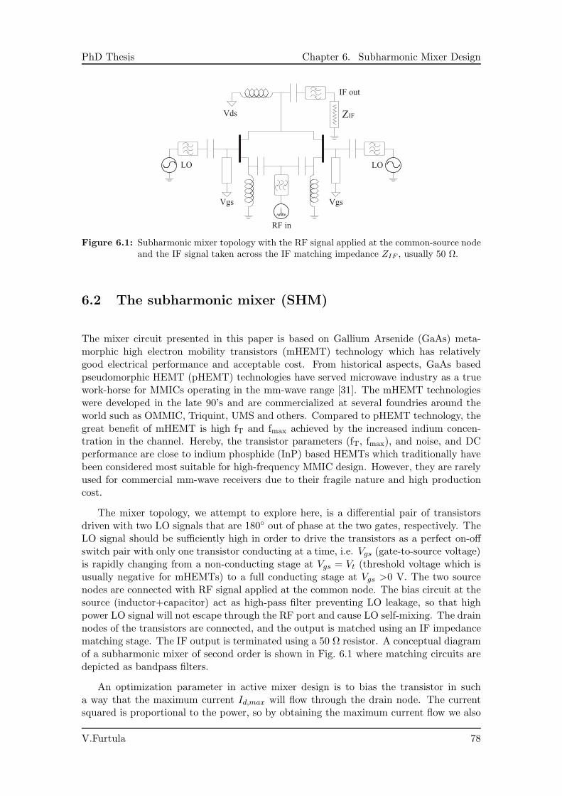
PhD Thesis Chapter 6. Subharmonic Mixer Design
Figure 6.1: Subharmonic mixer topology with the RF signal applied at the common-source nodeand the IF signal taken across the IF matching impedance ZIF , usually 50 Ω.
6.2 The subharmonic mixer (SHM)
The mixer circuit presented in this paper is based on Gallium Arsenide (GaAs) meta-morphic high electron mobility transistors (mHEMT) technology which has relativelygood electrical performance and acceptable cost. From historical aspects, GaAs basedpseudomorphic HEMT (pHEMT) technologies have served microwave industry as a truework-horse for MMICs operating in the mm-wave range [31]. The mHEMT technologieswere developed in the late 90’s and are commercialized at several foundries around theworld such as OMMIC, Triquint, UMS and others. Compared to pHEMT technology, thegreat benefit of mHEMT is high fT and fmax achieved by the increased indium concen-tration in the channel. Hereby, the transistor parameters (fT, fmax), and noise, and DCperformance are close to indium phosphide (InP) based HEMTs which traditionally havebeen considered most suitable for high-frequency MMIC design. However, they are rarelyused for commercial mm-wave receivers due to their fragile nature and high productioncost.
The mixer topology, we attempt to explore here, is a differential pair of transistorsdriven with two LO signals that are 180 out of phase at the two gates, respectively. TheLO signal should be sufficiently high in order to drive the transistors as a perfect on-offswitch pair with only one transistor conducting at a time, i.e. Vgs (gate-to-source voltage)is rapidly changing from a non-conducting stage at Vgs = Vt (threshold voltage which isusually negative for mHEMTs) to a full conducting stage at Vgs >0 V. The two sourcenodes are connected with RF signal applied at the common node. The bias circuit at thesource (inductor+capacitor) act as high-pass filter preventing LO leakage, so that highpower LO signal will not escape through the RF port and cause LO self-mixing. The drainnodes of the transistors are connected, and the output is matched using an IF impedancematching stage. The IF output is terminated using a 50 Ω resistor. A conceptual diagramof a subharmonic mixer of second order is shown in Fig. 6.1 where matching circuits aredepicted as bandpass filters.
An optimization parameter in active mixer design is to bias the transistor in sucha way that the maximum current Id,max will flow through the drain node. The currentsquared is proportional to the power, so by obtaining the maximum current flow we also
V.Furtula 78
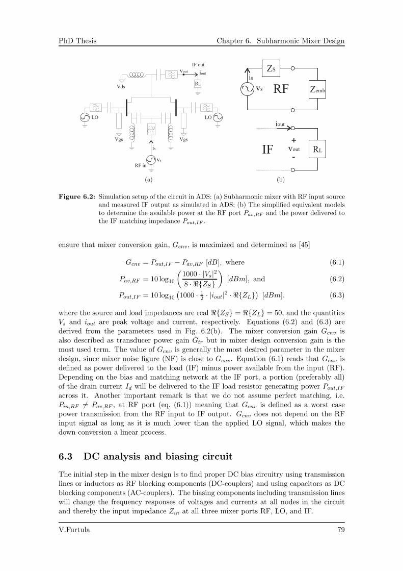
PhD Thesis Chapter 6. Subharmonic Mixer Design
(a) (b)
Figure 6.2: Simulation setup of the circuit in ADS: (a) Subharmonic mixer with RF input sourceand measured IF output as simulated in ADS; (b) The simplified equivalent modelsto determine the available power at the RF port Pav,RF and the power delivered tothe IF matching impedance Pout,IF .
ensure that mixer conversion gain, Gcnv, is maximized and determined as [45]
Gcnv = Pout,IF − Pav,RF [dB], where (6.1)
Pav,RF = 10 log10
(
1000 · |Vs|28 · ℜZS
)
[dBm], and (6.2)
Pout,IF = 10 log10(
1000 · 12 · |iout|2 · ℜZL
)
[dBm]. (6.3)
where the source and load impedances are real ℜZS = ℜZL = 50, and the quantitiesVs and iout are peak voltage and current, respectively. Equations (6.2) and (6.3) arederived from the parameters used in Fig. 6.2(b). The mixer conversion gain Gcnv isalso described as transducer power gain Gtr but in mixer design conversion gain is themost used term. The value of Gcnv is generally the most desired parameter in the mixerdesign, since mixer noise figure (NF) is close to Gcnv. Equation (6.1) reads that Gcnv isdefined as power delivered to the load (IF) minus power available from the input (RF).Depending on the bias and matching network at the IF port, a portion (preferably all)of the drain current Id will be delivered to the IF load resistor generating power Pout,IF
across it. Another important remark is that we do not assume perfect matching, i.e.Pin,RF 6= Pav,RF , at RF port (eq. (6.1)) meaning that Gcnv is defined as a worst casepower transmission from the RF input to IF output. Gcnv does not depend on the RFinput signal as long as it is much lower than the applied LO signal, which makes thedown-conversion a linear process.
6.3 DC analysis and biasing circuit
The initial step in the mixer design is to find proper DC bias circuitry using transmissionlines or inductors as RF blocking components (DC-couplers) and using capacitors as DCblocking components (AC-couplers). The biasing components including transmission lineswill change the frequency responses of voltages and currents at all nodes in the circuitand thereby the input impedance Zin at all three mixer ports RF, LO, and IF.
V.Furtula 79
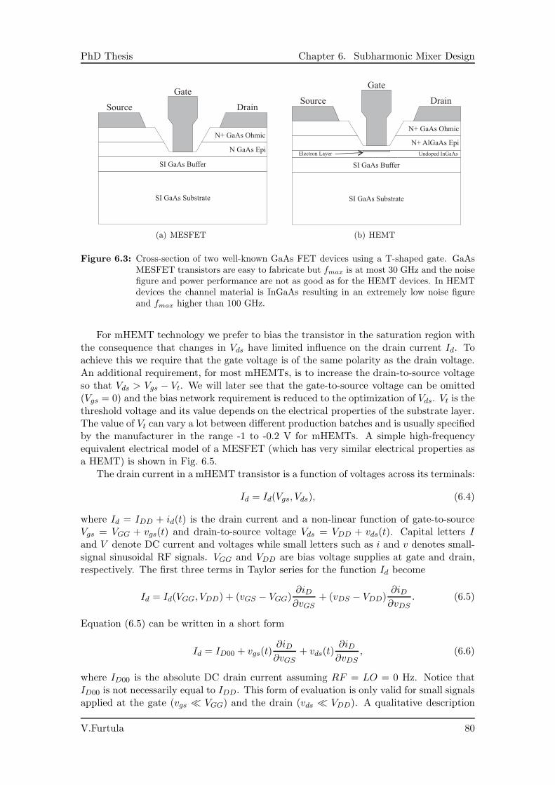
PhD Thesis Chapter 6. Subharmonic Mixer Design
(a) MESFET (b) HEMT
Figure 6.3: Cross-section of two well-known GaAs FET devices using a T-shaped gate. GaAsMESFET transistors are easy to fabricate but fmax is at most 30 GHz and the noisefigure and power performance are not as good as for the HEMT devices. In HEMTdevices the channel material is InGaAs resulting in an extremely low noise figureand fmax higher than 100 GHz.
For mHEMT technology we prefer to bias the transistor in the saturation region withthe consequence that changes in Vds have limited influence on the drain current Id. Toachieve this we require that the gate voltage is of the same polarity as the drain voltage.An additional requirement, for most mHEMTs, is to increase the drain-to-source voltageso that Vds > Vgs − Vt. We will later see that the gate-to-source voltage can be omitted(Vgs = 0) and the bias network requirement is reduced to the optimization of Vds. Vt is thethreshold voltage and its value depends on the electrical properties of the substrate layer.The value of Vt can vary a lot between different production batches and is usually specifiedby the manufacturer in the range -1 to -0.2 V for mHEMTs. A simple high-frequencyequivalent electrical model of a MESFET (which has very similar electrical properties asa HEMT) is shown in Fig. 6.5.
The drain current in a mHEMT transistor is a function of voltages across its terminals:
Id = Id(Vgs, Vds), (6.4)
where Id = IDD + id(t) is the drain current and a non-linear function of gate-to-sourceVgs = VGG + vgs(t) and drain-to-source voltage Vds = VDD + vds(t). Capital letters Iand V denote DC current and voltages while small letters such as i and v denotes small-signal sinusoidal RF signals. VGG and VDD are bias voltage supplies at gate and drain,respectively. The first three terms in Taylor series for the function Id become
Id = Id(VGG, VDD) + (vGS − VGG)∂iD∂vGS
+ (vDS − VDD)∂iD∂vDS
. (6.5)
Equation (6.5) can be written in a short form
Id = ID00 + vgs(t)∂iD∂vGS
+ vds(t)∂iD∂vDS
, (6.6)
where ID00 is the absolute DC drain current assuming RF = LO = 0 Hz. Notice thatID00 is not necessarily equal to IDD. This form of evaluation is only valid for small signalsapplied at the gate (vgs ≪ VGG) and the drain (vds ≪ VDD). A qualitative description
V.Furtula 80
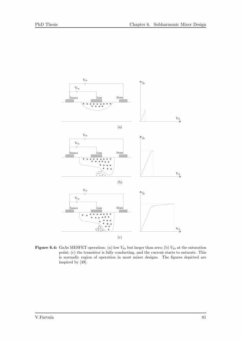
PhD Thesis Chapter 6. Subharmonic Mixer Design
(a)
(b)
(c)
Figure 6.4: GaAs MESFET operation: (a) low Vds but larger than zero; (b) Vds at the saturationpoint; (c) the transistor is fully conducting, and the current starts to saturate. Thisis normally region of operation in most mixer designs. The figures depicted areinspired by [49].
V.Furtula 81
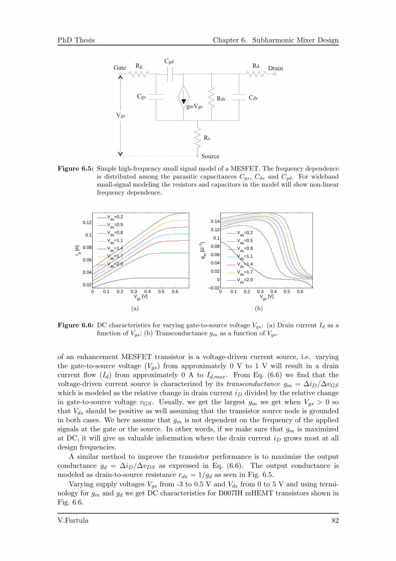
PhD Thesis Chapter 6. Subharmonic Mixer Design
Figure 6.5: Simple high-frequency small signal model of a MESFET. The frequency dependenceis distributed among the parasitic capacitances Cgs, Cds and Cgd. For widebandsmall-signal modeling the resistors and capacitors in the model will show non-linearfrequency dependence.
0 0.1 0.2 0.3 0.4 0.5 0.6
0.02
0.04
0.06
0.08
0.1
0.12
I d [A]
Vgs
[V]
V
ds=0.2
Vds
=0.5
Vds
=0.8
Vds
=1.1
Vds
=1.4
Vds
=1.7
Vds
=2.0
(a)
0 0.1 0.2 0.3 0.4 0.5 0.6−0.02
0
0.02
0.04
0.06
0.08
0.1
0.12
0.14
g m [Ω
−1 ]
Vgs
[V]
Vds
=0.2
Vds
=0.5
Vds
=0.8
Vds
=1.1
Vds
=1.4
Vds
=1.7
Vds
=2.0
(b)
Figure 6.6: DC characteristics for varying gate-to-source voltage Vgs: (a) Drain current Id as afunction of Vgs; (b) Transconductance gm as a function of Vgs.
of an enhancement MESFET transistor is a voltage-driven current source, i.e. varyingthe gate-to-source voltage (Vgs) from approximately 0 V to 1 V will result in a draincurrent flow (Id) from approximately 0 A to Id,max. From Eq. (6.6) we find that thevoltage-driven current source is characterized by its transconductance gm = ∆iD/∆vGS
which is modeled as the relative change in drain current iD divided by the relative changein gate-to-source voltage vGS . Usually, we get the largest gm we get when Vgs > 0 sothat Vds should be positive as well assuming that the transistor source node is groundedin both cases. We here assume that gm is not dependent on the frequency of the appliedsignals at the gate or the source. In other words, if we make sure that gm is maximizedat DC, it will give us valuable information where the drain current iD grows most at alldesign frequencies.
A similar method to improve the transistor performance is to maximize the outputconductance gd = ∆iD/∆vDS as expressed in Eq. (6.6). The output conductance ismodeled as drain-to-source resistance rds = 1/gd as seen in Fig. 6.5.
Varying supply voltages Vgs from -3 to 0.5 V and Vds from 0 to 5 V and using termi-nology for gm and gd we get DC characteristics for D007IH mHEMT transistors shown inFig. 6.6.
V.Furtula 82
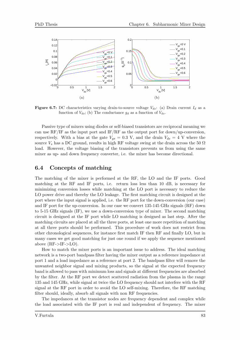
PhD Thesis Chapter 6. Subharmonic Mixer Design
0 0.5 1 1.5 2−0.02
0
0.02
0.04
0.06
0.08
0.1
0.12
0.14
I d [A]
Vds
[V]
Vgs
=0 V
Vgs
=0.1
Vgs
=0.2
Vgs
=0.3
Vgs
=0.4
Vgs
=0.5
Vgs
=0.6
(a)
0 0.5 1 1.5 20
0.05
0.1
0.15
0.2
g d [Ω−
1 ]
Vds
[V]
Vgs
=0 V
Vgs
=0.1
Vgs
=0.2
Vgs
=0.3
Vgs
=0.4
Vgs
=0.5
Vgs
=0.6
(b)
Figure 6.7: DC characteristics varying drain-to-source voltage Vds: (a) Drain current Id as afunction of Vds; (b) The conductance gd as a function of Vds.
Passive type of mixers using diodes or self-biased transistors are reciprocal meaning wecan use RF/IF as the input port and IF/RF as the output port for down/up-conversion,respectively. With a bias at the gate Vgs = 0.3 V, and the drain Vds = 4 V where thesource Vs has a DC ground, results in high RF voltage swing at the drain across the 50 Ωload. However, the voltage biasing of the transistors prevents us from using the samemixer as up- and down frequency converter, i.e. the mixer has become directional.
6.4 Concepts of matching
The matching of the mixer is performed at the RF, the LO and the IF ports. Goodmatching at the RF and IF ports, i.e. return loss less than 10 dB, is necessary forminimizing conversion losses while matching at the LO port is necessary to reduce theLO power drive and thereby the LO leakage. The first matching circuit is designed at theport where the input signal is applied, i.e. the RF port for the down-conversion (our case)and IF port for the up-conversion. In our case we convert 135-145 GHz signals (RF) downto 5-15 GHz signals (IF), we use a down-conversion type of mixer. The second matchingcircuit is designed at the IF port while LO matching is designed as last step. After thematching circuits are placed at all the three ports, at least one more repetition of matchingat all three ports should be performed. This procedure of work does not restrict fromother chronological sequences, for instance first match IF then RF and finally LO, but inmany cases we get good matching for just one round if we apply the sequence mentionedabove (RF->IF->LO).
How to match the mixer ports is an important issue to address. The ideal matchingnetwork is a two-port bandpass filter having the mixer output as a reference impedance atport 1 and a load impedance as a reference at port 2. The bandpass filter will remove theunwanted neighbor signal and mixing products, so the signal at the expected frequencyband is allowed to pass with minimum loss and signals at different frequencies are absorbedby the filter. At the RF port we detect scattered radiation from the plasma in the range135 and 145 GHz, while signal at twice the LO frequency should not interfere with the RFsignal at the RF port in order to avoid the LO self-mixing. Therefore, the RF matchingfilter should, ideally, absorb all signals with non RF frequencies.
The impedances at the transistor nodes are frequency dependent and complex whilethe load associated with the IF port is real and independent of frequency. The mixer
V.Furtula 83
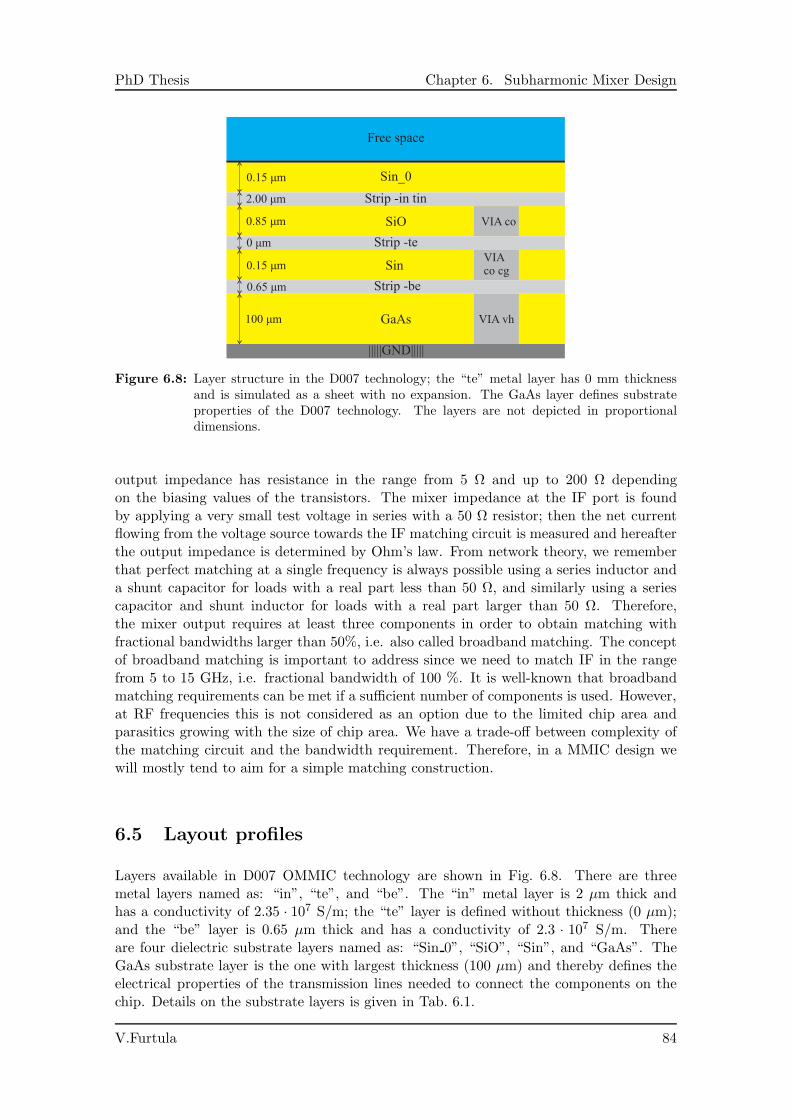
PhD Thesis Chapter 6. Subharmonic Mixer Design
Free space
Strip -in tin
Sin_0
VIA co
Strip -te
SiO
SinVIAco cg
Strip -be
GaAs VIA vh
|||||GND|||||
100 mμ
0.65 mμ
0.15 mμ
0 mμ
0.85 mμ
2.00 mμ
0.15 mμ
Figure 6.8: Layer structure in the D007 technology; the “te” metal layer has 0 mm thicknessand is simulated as a sheet with no expansion. The GaAs layer defines substrateproperties of the D007 technology. The layers are not depicted in proportionaldimensions.
output impedance has resistance in the range from 5 Ω and up to 200 Ω dependingon the biasing values of the transistors. The mixer impedance at the IF port is foundby applying a very small test voltage in series with a 50 Ω resistor; then the net currentflowing from the voltage source towards the IF matching circuit is measured and hereafterthe output impedance is determined by Ohm’s law. From network theory, we rememberthat perfect matching at a single frequency is always possible using a series inductor anda shunt capacitor for loads with a real part less than 50 Ω, and similarly using a seriescapacitor and shunt inductor for loads with a real part larger than 50 Ω. Therefore,the mixer output requires at least three components in order to obtain matching withfractional bandwidths larger than 50%, i.e. also called broadband matching. The conceptof broadband matching is important to address since we need to match IF in the rangefrom 5 to 15 GHz, i.e. fractional bandwidth of 100 %. It is well-known that broadbandmatching requirements can be met if a sufficient number of components is used. However,at RF frequencies this is not considered as an option due to the limited chip area andparasitics growing with the size of chip area. We have a trade-off between complexity ofthe matching circuit and the bandwidth requirement. Therefore, in a MMIC design wewill mostly tend to aim for a simple matching construction.
6.5 Layout profiles
Layers available in D007 OMMIC technology are shown in Fig. 6.8. There are threemetal layers named as: “in”, “te”, and “be”. The “in” metal layer is 2 µm thick andhas a conductivity of 2.35 · 107 S/m; the “te” layer is defined without thickness (0 µm);and the “be” layer is 0.65 µm thick and has a conductivity of 2.3 · 107 S/m. Thereare four dielectric substrate layers named as: “Sin 0”, “SiO”, “Sin”, and “GaAs”. TheGaAs substrate layer is the one with largest thickness (100 µm) and thereby defines theelectrical properties of the transmission lines needed to connect the components on thechip. Details on the substrate layers is given in Tab. 6.1.
V.Furtula 84
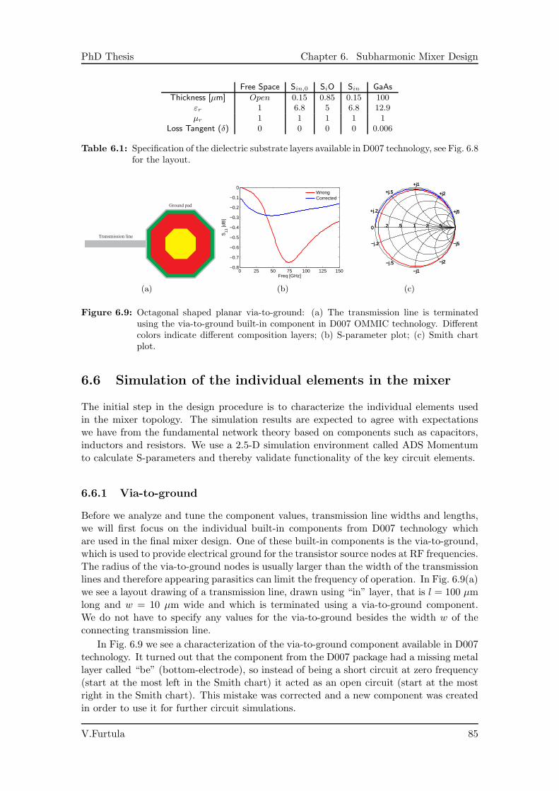
PhD Thesis Chapter 6. Subharmonic Mixer Design
Free Space Sin,0 SiO Sin GaAs
Thickness [µm] Open 0.15 0.85 0.15 100εr 1 6.8 5 6.8 12.9µr 1 1 1 1 1
Loss Tangent (δ) 0 0 0 0 0.006
Table 6.1: Specification of the dielectric substrate layers available in D007 technology, see Fig. 6.8for the layout.
Transmission line
Ground pad
(a)
0 25 50 75 100 125 150−0.8
−0.7
−0.6
−0.5
−0.4
−0.3
−0.2
−0.1
0
S11
[dB
]
Freq [GHz]
WrongCorrected
(b)
0
+j.2
−j.2
+j.5
−j.5
+j1
−j1
+j2
−j2
+j5
−j5
.2 .5 1 2 50
+j.2
−j.2
+j.5
−j.5
+j1
−j1
+j2
−j2
+j5
−j5
.2 .5 1 2 5
(c)
Figure 6.9: Octagonal shaped planar via-to-ground: (a) The transmission line is terminatedusing the via-to-ground built-in component in D007 OMMIC technology. Differentcolors indicate different composition layers; (b) S-parameter plot; (c) Smith chartplot.
6.6 Simulation of the individual elements in the mixer
The initial step in the design procedure is to characterize the individual elements usedin the mixer topology. The simulation results are expected to agree with expectationswe have from the fundamental network theory based on components such as capacitors,inductors and resistors. We use a 2.5-D simulation environment called ADS Momentumto calculate S-parameters and thereby validate functionality of the key circuit elements.
6.6.1 Via-to-ground
Before we analyze and tune the component values, transmission line widths and lengths,we will first focus on the individual built-in components from D007 technology whichare used in the final mixer design. One of these built-in components is the via-to-ground,which is used to provide electrical ground for the transistor source nodes at RF frequencies.The radius of the via-to-ground nodes is usually larger than the width of the transmissionlines and therefore appearing parasitics can limit the frequency of operation. In Fig. 6.9(a)we see a layout drawing of a transmission line, drawn using “in” layer, that is l = 100 µmlong and w = 10 µm wide and which is terminated using a via-to-ground component.We do not have to specify any values for the via-to-ground besides the width w of theconnecting transmission line.
In Fig. 6.9 we see a characterization of the via-to-ground component available in D007technology. It turned out that the component from the D007 package had a missing metallayer called “be” (bottom-electrode), so instead of being a short circuit at zero frequency(start at the most left in the Smith chart) it acted as an open circuit (start at the mostright in the Smith chart). This mistake was corrected and a new component was createdin order to use it for further circuit simulations.
V.Furtula 85
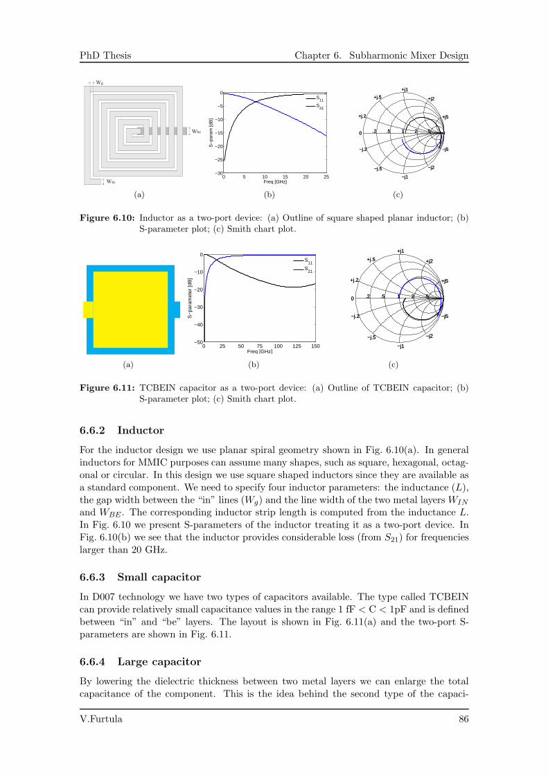
PhD Thesis Chapter 6. Subharmonic Mixer Design
Win
Wbe
Wg
(a)
0 5 10 15 20 25−30
−25
−20
−15
−10
−5
0
S−
para
m [d
B]
Freq [GHz]
S11
S21
(b)
0
+j.2
−j.2
+j.5
−j.5
+j1
−j1
+j2
−j2
+j5
−j5
.2 .5 1 2 50
+j.2
−j.2
+j.5
−j.5
+j1
−j1
+j2
−j2
+j5
−j5
.2 .5 1 2 5
(c)
Figure 6.10: Inductor as a two-port device: (a) Outline of square shaped planar inductor; (b)S-parameter plot; (c) Smith chart plot.
(a)
0 25 50 75 100 125 150−50
−40
−30
−20
−10
0
S−
para
met
er [d
B]
Freq [GHz]
S11
S21
(b)
0
+j.2
−j.2
+j.5
−j.5
+j1
−j1
+j2
−j2
+j5
−j5
.2 .5 1 2 50
+j.2
−j.2
+j.5
−j.5
+j1
−j1
+j2
−j2
+j5
−j5
.2 .5 1 2 5
(c)
Figure 6.11: TCBEIN capacitor as a two-port device: (a) Outline of TCBEIN capacitor; (b)S-parameter plot; (c) Smith chart plot.
6.6.2 Inductor
For the inductor design we use planar spiral geometry shown in Fig. 6.10(a). In generalinductors for MMIC purposes can assume many shapes, such as square, hexagonal, octag-onal or circular. In this design we use square shaped inductors since they are available asa standard component. We need to specify four inductor parameters: the inductance (L),the gap width between the “in” lines (Wg) and the line width of the two metal layers WIN
and WBE . The corresponding inductor strip length is computed from the inductance L.In Fig. 6.10 we present S-parameters of the inductor treating it as a two-port device. InFig. 6.10(b) we see that the inductor provides considerable loss (from S21) for frequencieslarger than 20 GHz.
6.6.3 Small capacitor
In D007 technology we have two types of capacitors available. The type called TCBEINcan provide relatively small capacitance values in the range 1 fF < C < 1pF and is definedbetween “in” and “be” layers. The layout is shown in Fig. 6.11(a) and the two-port S-parameters are shown in Fig. 6.11.
6.6.4 Large capacitor
By lowering the dielectric thickness between two metal layers we can enlarge the totalcapacitance of the component. This is the idea behind the second type of the capaci-
V.Furtula 86
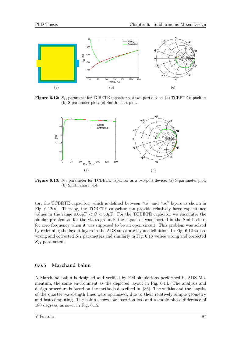
PhD Thesis Chapter 6. Subharmonic Mixer Design
(a)
0 25 50 75 100 125 150−50
−40
−30
−20
−10
0
S11
[dB
]Freq [GHz]
WrongCorrected
(b)
0
+j.2
−j.2
+j.5
−j.5
+j1
−j1
+j2
−j2
+j5
−j5
.2 .5 1 2 50
+j.2
−j.2
+j.5
−j.5
+j1
−j1
+j2
−j2
+j5
−j5
.2 .5 1 2 5
(c)
Figure 6.12: S11 parameter for TCBETE capacitor as a two-port device: (a) TCBETE capacitor;(b) S-parameter plot; (c) Smith chart plot.
0 25 50 75 100 125 150−5
−4
−3
−2
−1
0
S21
[dB
]
Freq [GHz]
WrongCorrected
(a)
0
+j.2
−j.2
+j.5
−j.5
+j1
−j1
+j2
−j2
+j5
−j5
.2 .5 1 2 50
+j.2
−j.2
+j.5
−j.5
+j1
−j1
+j2
−j2
+j5
−j5
.2 .5 1 2 5
(b)
Figure 6.13: S21 parameter for TCBETE capacitor as a two-port device: (a) S-parameter plot;(b) Smith chart plot.
tor, the TCBETE capacitor, which is defined between “te” and “be” layers as shown inFig. 6.12(a). Thereby, the TCBETE capacitor can provide relatively large capacitancevalues in the range 0.06pF < C < 50pF. For the TCBETE capacitor we encounter thesimilar problem as for the via-to-ground: the capacitor was shorted in the Smith chartfor zero frequency when it was supposed to be an open circuit. This problem was solvedby redefining the layout layers in the ADS substrate layout definition. In Fig. 6.12 we seewrong and corrected S11 parameters and similarly in Fig. 6.13 we see wrong and correctedS21 parameters.
6.6.5 Marchand balun
A Marchand balun is designed and verified by EM simulations performed in ADS Mo-mentum, the same environment as the depicted layout in Fig. 6.14. The analysis anddesign procedure is based on the methods described in [36]. The widths and the lengthsof the quarter wavelength lines were optimized, due to their relatively simple geometryand fast computing. The balun shows low insertion loss and a stable phase difference of180 degrees, as sown in Fig. 6.15.
V.Furtula 87
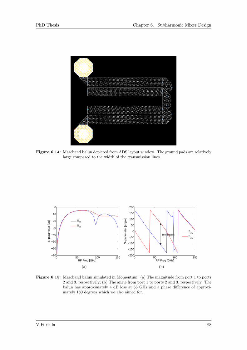
PhD Thesis Chapter 6. Subharmonic Mixer Design
Figure 6.14: Marchand balun depicted from ADS layout window. The ground pads are relativelylarge compared to the width of the transmission lines.
0 50 100 150−70
−60
−50
−40
−30
−20
−10
0
RF Freq [GHz]
S−
para
met
er [d
B]
S31
S21
(a)
0 50 100 150−200
−150
−100
−50
0
50
100
150
200
RF Freq [GHz]
S−
para
met
er [a
ngle
]
S31
S21
180 degrees
(b)
Figure 6.15: Marchand balun simulated in Momentum: (a) The magnitude from port 1 to ports2 and 3, respectively; (b) The angle from port 1 to ports 2 and 3, respectively. Thebalun has approximately 4 dB loss at 65 GHz and a phase difference of approxi-mately 180 degrees which we also aimed for.
V.Furtula 88
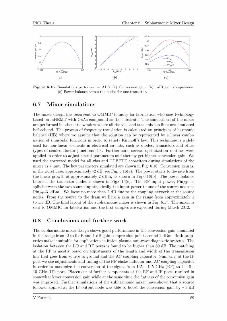
PhD Thesis Chapter 6. Subharmonic Mixer Design
135 140 145−2.5
−2
−1.5
−1
−0.5
0
RF Freq [GHz]
Con
vers
ion
gain
[dB
]
(a)
−12 −10 −8 −6 −4 −2 0 2 4 6 8−8
−6
−4
−2
0
2
4
6
8
Pin
[dBm]
Pou
t [dB
m]
(b)
135 140 145−62
−61.5
−61
−60.5
−60
−59.5
−59
−58.5
RF Freq [GHz]
Pow
er [d
Bm
]
Pins1
Poutd1
PinRF
−3
(c)
Figure 6.16: Simulations performed in ADS: (a) Conversion gain; (b) 1-dB gain compression;(c) Power balance across the nodes for one transistor.
6.7 Mixer simulations
The mixer design has been sent to OMMIC foundry for fabrication who uses technologybased on mHEMT with GaAs compound as the substrate. The simulations of the mixerare performed in schematic window where all the vias and transmission lines are simulatedbeforehand. The process of frequency translation is calculated on principles of harmonicbalance (HB) where we assume that the solution can be represented by a linear combi-nation of sinusoidal functions in order to satisfy Kirchoff’s law. This technique is widelyused for non-linear elements in electrical circuits, such as diodes, transistors and othertypes of semiconductor junctions [49]. Furthermore, several optimization routines wereapplied in order to adjust circuit parameters and thereby get higher conversion gain. Weused the corrected model for all vias and TCBETE capacitors during simulations of themixer as a unit. The key parameters simulated are shown in Fig. 6.16. Conversion gain is,in the worst case, approximately -2 dB, see Fig. 6.16(a). The power starts to deviate fromthe linear growth at approximately 2 dBm, as shown in Fig.6.16(b). The power balancebetween the transistor nodes is shown in Fig.6.16(c). The RF input power, PinRF , issplit between the two source inputs, ideally the input power to one of the source nodes isPinRF -3 [dBm]. We loose no more than 2 dB due to the coupling network at the sourcenodes. From the source to the drain we have a gain in the range from approximately 1to 1.5 dB. The final layout of the subharmonic mixer is shown in Fig. 6.17. The mixer issent to OMMIC for fabrication and the first samples are expected during March 2012.
6.8 Conclusions and further work
The subharmonic mixer design shows good performance in the conversion gain simulatedin the range from -2 to 0 dB and 1-dB gain compression point around 2 dBm. Both prop-erties make it suitable for applications in fusion plasma mm-wave diagnostic systems. Theisolation between the LO and RF ports is found to be higher than 80 dB. The matchingat the RF is mostly based on adjustments of the length and width of the transmissionline that goes from source to ground and the AC coupling capacitor. Similarly, at the IFport we use adjustments and tuning of the RF choke inductor and AC coupling capacitorin order to maximize the conversion of the signal from 135 - 145 GHz (RF) to the 5 -15 GHz (IF) port. Placement of further components at the RF and IF ports resulted insomewhat lower conversion gain while at the same time the flatness of the conversion gainwas improved. Further simulations of the subharmonic mixer have shown that a sourcefollower applied at the IF output node was able to boost the conversion gain by ∼3 dB
V.Furtula 89
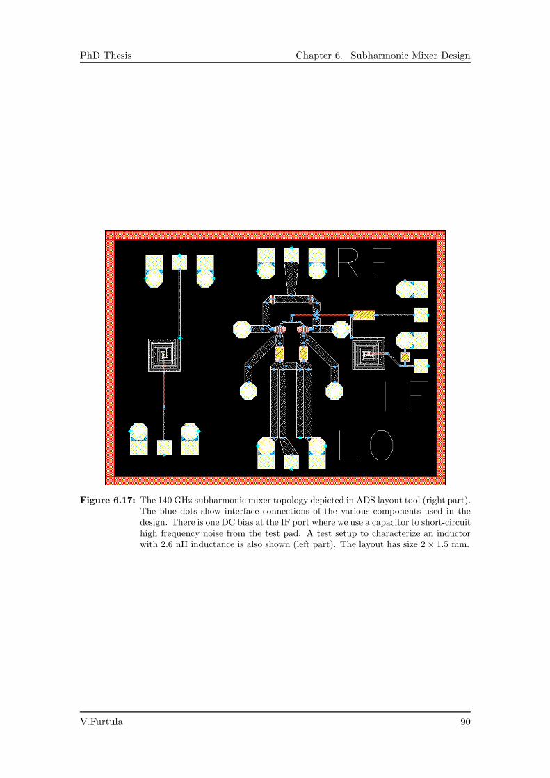
PhD Thesis Chapter 6. Subharmonic Mixer Design
Figure 6.17: The 140 GHz subharmonic mixer topology depicted in ADS layout tool (right part).The blue dots show interface connections of the various components used in thedesign. There is one DC bias at the IF port where we use a capacitor to short-circuithigh frequency noise from the test pad. A test setup to characterize an inductorwith 2.6 nH inductance is also shown (left part). The layout has size 2× 1.5 mm.
V.Furtula 90

PhD Thesis Chapter 6. Subharmonic Mixer Design
around 140 GHz and by ∼1 dB at the edges of the mixer design range 135 - 145 GHz.
V.Furtula 91

Chapter 7
Summary and Future Work
Through this work we have demonstrated functionality and introduced improvements ofthe millimeter wave receivers used to detect scattered radiation in fusion plasmas. Thefrequency of operation is mainly in the D band, it spans from 100 to 110 GHz for CTSanalysis and up to 145 GHz for NTM analysis. This work was primarily dedicated tomillimeter wave receivers with the objective to detect scattered radiation associated todynamics of fast ions.
Conceptual studies on ITER have shown that 60 GHz probing beam is sufficient todetect fast ions. We find it important to resolve the near parallel velocity components ofthe fast ion distribution in ITER. We have presented a compact solution of an antennaarray that can be accommodated on the ITER HFS. The antenna array, consisting of amirror assembly accompanied with a test horn, has been verified experimentally with a1:1 mock-up.
The individual components of the CTS receiver at ASDEX Upgrade and their per-formance have been presented. The AUG receiver uses a heterodyne scheme, it convertsinput signals in the RF range from 100 to 110 GHz down to the IF range from 5 to 15 GHzusing a mixer. We have measured losses in the range from 10 to 26 dB in the receiver RFline. One of the reasons for high losses is the notch filter that must be integrated into thereceiver system in order to reject the strong probing beam. Extensive study on this topicis performed, and we are able to deliver notch filters with 1 GHz rejection bandwidth andmore than 25 GHz passband bandwidth for multi gyrotron operations. Similarly, we candeliver notch filters with 150 MHz rejection bandwidth and more than 14 GHz passbandbandwidth for single gyrotron operations. Both achievements are reported for the firsttime in the community of fusion diagnostics.
A mixer with small conversion loss is also desired in fusion experiments, since noamplifiers in the D-band are commercially available for plasma diagnostics. A way tokeep the system noise figure low is to design a mixer with low conversion loss. We havedesigned a mixer for NTM applications with center frequency at 140 GHz, conversion losssimulated in the range from 0 to 2 dB, and 1-dB gain compression point around 2 dBm.The mixer layout proposal is sent to OMMIC foundry for fabrication.
The next step CTS receivers should use custom-made active components such asmixers, amplifiers, and VCVAs integrated in one unit with an interface that is easy toconnect with solid structures such as waveguides. The most promising solutions useminiature patch antennas to couple fields from a microstrip line into a waveguide, alarge research area at Chalmers University, and possibly, a step closer to supreme CTSreceivers. Furthermore, a different way to improve mm-wave receiver is to design all thepassive waveguide components in the RF line as a one large component. By this means,
93

PhD Thesis Chapter 7. Summary and Future Work
we reduce easily insertion loss by 5 dB, since the imperfect junction interfaces betweenthe components are no longer there. All RF components are needed during experiments,so by using an integrated RF branch flexibility of the receiver will degrade only slightlywhile modulation of the received signal will improve considerably.
V.Furtula 94

Appendix A
Microwave Two-Port Network
A two-port network presented in the Fig. A.1 is the most common setup to measureelectrical wave properties of an RF component, particulary when more complicated circuitsystems need to be analyzed. Characterization of a two-port network prescribes that thetwo-port scattering parameters, S-parameters, are calculated. Dealing with RF circuitsthere are two basic approaches to two-port parameters, either scattering parameters -also called S-parameters - or the traditional admittance, impedance and hybrid types -Y,Z,H,G - of small-signal parameters. S-parameters relate a set of incident and reflectedwave quantities that are defined in terms of port voltages and currents. They have theadvantage of being relatively simple to measure at high frequencies. The more traditionalparameter types constrain port voltages and currents by terminal conditions that areopen or short circuits, and this is somewhat difficult to establish at high frequencies. Inthe following text we will define basic principles of the generalized transmission line andafterwards we will focus on derivation of the S-parameters for some fundamental circuitconfigurations.
A.0.1 A General Transmission Line
A uniform transmission line is defined by identical dimensions and electrical propertiesat all planes transverse to the direction of propagation. Also, we are able to apply ACcircuit concepts to the lines whose lengths are not negligible compared to the operatingwavelength. A general transmission line has both voltage and current waves propagatingthrough the system. Defining the propagation constant as γ = α+ jβ we find the voltageand the current waves as
V = V+0 exp(−γz) +V−
0 exp(+γz) = V+ +V− (A.1)
I = I+0 exp(−γz)− I−0 exp(+γz) = I+ − I−. (A.2)
ZG
VG
I1 I2
Z =Z01 0 Z =Z02 0 ZL
+
-
V1 V2
Port 1 Port 2(Input) (Output)
+
-
A linear
two-port
network
Figure A.1: A linear two-port network and its associated input and output quantities.
95
PhD Thesis Appendix A. Microwave Two-Port Network
Z ,alpha,beta0
zz=0 z=l
Figure A.2: A transmission line with length z = l.
The notation V+(z = 0) = V+0 is the forward traveling voltage wave and V−(z = 0) =
V−
0 is the backward traveling voltage wave, see Fig. A.2. Similarly, we have the samedesignation for the current traveling waves. Notice that both V and I are vectors andtypically have a direction along the z-axis. The ratio of the forward to the backwardvoltage (or current) is defined as the reflection coefficient Γ
Γ ≡ Backward voltage(or current) at pt. z
Forward voltage(or current) at pt. z=
V−
V+=
I−
I+(A.3)
The power across the transmission line is given as
P = ℜ(VI∗). (A.4)
Using the fact that V+ = I+Z0 and V− = ΓV+ then we find that
P = ℜ[
(1− |Γ|2 + Γ− Γ∗)(V +)2
Z∗
0
]
, (A.5)
where we used complex conjugate formalism ΓΓ∗ = |Γ|2 and V+V+∗ = (V +)2. In highfrequency lines Z0 can be considered as pure real and the above expression reduces to
P = P+(1− |Γ|2) = P+ − P−, (A.6)
since Γ−Γ∗ is imaginary. From the Eq. (A.6) we find that the ratio between the backwardand forward power is the absolute voltage (or current) coefficient squared given as
P− = |Γ|2P+. (A.7)
Another advantage of real Z0 is the fact that V+ and I+ are in phase resulting in
P+ =(V +)2
Z0=
(V +0 )2
Z0exp(−2αz) (A.8)
P− =(V +
0 )2
Z0|Γ|2 exp(−2αz) (A.9)
Using equations Eq. (A.8) and Eq. (A.9) we can determine the two-port scattering param-eters from the physical quantities Z0, ZG and γ. But we still need to find an expressionfor the forward traveling voltage wave V +
0 . Applying Kirchhoff’s voltage law at the inputthe forward voltage wave equation may be written as
V+0 =
VG(1− ΓG)
2(1 − ΓGΓL exp(−2γl)). (A.10)
The reflection coefficients at the generator ΓG and the load ΓL are defined as
ΓG =ZG − Z0
ZG + Z0and ΓL =
ZL − Z0
ZL + Z0. (A.11)
V.Furtula 96
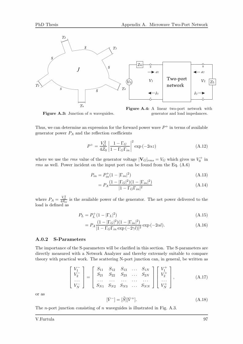
PhD Thesis Appendix A. Microwave Two-Port Network
J
S
SS
S
S
T1
Tn
T4
T3
T2
Figure A.3: Junction of n waveguides.
ZG
VG V1 V2Two-port
network
+ +
-
ZL
-
a1
b2b1
a2
Figure A.4: A linear two-port network withgenerator and load impedances.
Thus, we can determine an expression for the forward power wave P+ in terms of availablegenerator power PA and the reflection coefficients
P+ =V 2G
4Z0
∣
∣
∣
∣
1− ΓG
1− ΓGΓin
∣
∣
∣
∣
2
exp (−2αz) (A.12)
where we use the rms value of the generator voltage |VG|rms = VG which gives us V +0 in
rms as well. Power incident on the input port can be found from the Eq. (A.6)
Pin = P+in(1− |Γin|2) (A.13)
= PA(1− |ΓG|2)(1− |Γin|2)
|1− ΓGΓin|2(A.14)
where PA =V 2G
4RGis the available power of the generator. The net power delivered to the
load is defined as
PL = P+L (1− |ΓL|2) (A.15)
= PA(1− |ΓG|2)(1 − |Γin|2)|1− ΓGΓin exp (−2γl)|2 exp (−2αl). (A.16)
A.0.2 S-Parameters
The importance of the S-parameters will be clarified in this section. The S-parameters aredirectly measured with a Network Analyzer and thereby extremely suitable to comparetheory with practical work. The scattering N-port junction can, in general, be written as
V −
1
V −
2
. . .V −
N
=
S11 S12 S13 . . . S1NS21 S22 S23 . . . S2N. . . . . . . . . . . . . . .SN1 SN2 SN3 . . . SNN
V +1
V +2
. . .V +N
, (A.17)
or as
[V −] = [ ¯S][V +]. (A.18)
The n-port junction consisting of n waveguides is illustrated in Fig. A.3.
V.Furtula 97
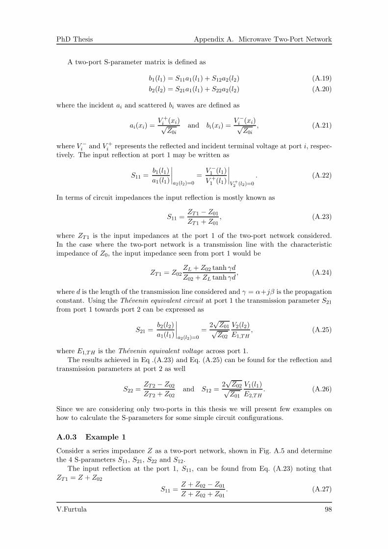
PhD Thesis Appendix A. Microwave Two-Port Network
A two-port S-parameter matrix is defined as
b1(l1) = S11a1(l1) + S12a2(l2) (A.19)
b2(l2) = S21a1(l1) + S22a2(l2) (A.20)
where the incident ai and scattered bi waves are defined as
ai(xi) =V +i (xi)√Z0i
and bi(xi) =V −
i (xi)√Z0i
, (A.21)
where V −
i and V +i represents the reflected and incident terminal voltage at port i, respec-
tively. The input reflection at port 1 may be written as
S11 =b1(l1)
a1(l1)
∣
∣
∣
∣
a2(l2)=0
=V −
1 (l1)
V +1 (l1)
∣
∣
∣
∣
V +
2(l2)=0
. (A.22)
In terms of circuit impedances the input reflection is mostly known as
S11 =ZT1 − Z01
ZT1 + Z01, (A.23)
where ZT1 is the input impedances at the port 1 of the two-port network considered.In the case where the two-port network is a transmission line with the characteristicimpedance of Z0, the input impedance seen from port 1 would be
ZT1 = Z02ZL + Z02 tanh γd
Z02 + ZL tanh γd, (A.24)
where d is the length of the transmission line considered and γ = α+jβ is the propagationconstant. Using the Thevenin equivalent circuit at port 1 the transmission parameter S21from port 1 towards port 2 can be expressed as
S21 =b2(l2)
a1(l1)
∣
∣
∣
∣
a2(l2)=0
=2√Z01√Z02
V2(l2)
E1,TH, (A.25)
where E1,TH is the Thevenin equivalent voltage across port 1.
The results achieved in Eq .(A.23) and Eq. (A.25) can be found for the reflection andtransmission parameters at port 2 as well
S22 =ZT2 − Z02
ZT2 + Z02and S12 =
2√Z02√Z01
V1(l1)
E2,TH. (A.26)
Since we are considering only two-ports in this thesis we will present few examples onhow to calculate the S-parameters for some simple circuit configurations.
A.0.3 Example 1
Consider a series impedance Z as a two-port network, shown in Fig. A.5 and determinethe 4 S-parameters S11, S21, S22 and S12.
The input reflection at the port 1, S11, can be found from Eq. (A.23) noting thatZT1 = Z + Z02
S11 =Z + Z02 − Z01
Z + Z02 + Z01. (A.27)
V.Furtula 98
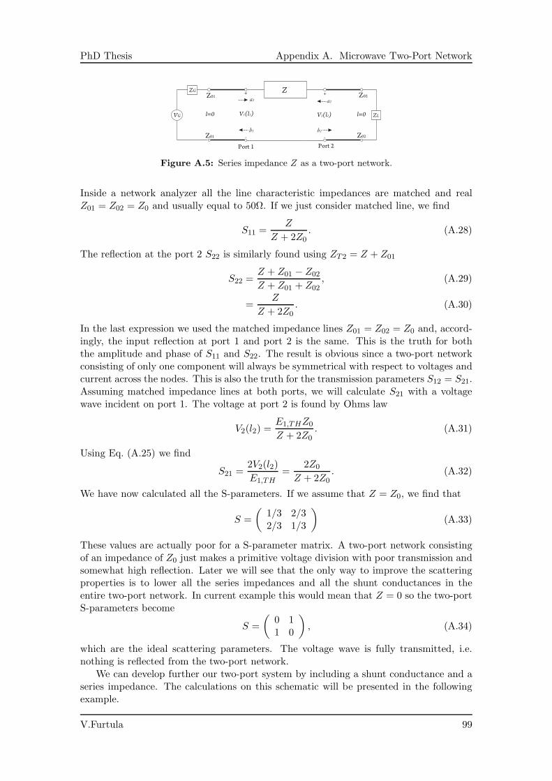
PhD Thesis Appendix A. Microwave Two-Port Network
ZG
VG ZL
Z
V (l )1 1
+
-
a1
b1
+
b2
a2
-
V (l )2 2l=0 l=0
Port 1 Port 2
Z01
Z01
Z02
Z02
Figure A.5: Series impedance Z as a two-port network.
Inside a network analyzer all the line characteristic impedances are matched and realZ01 = Z02 = Z0 and usually equal to 50Ω. If we just consider matched line, we find
S11 =Z
Z + 2Z0. (A.28)
The reflection at the port 2 S22 is similarly found using ZT2 = Z + Z01
S22 =Z + Z01 − Z02
Z + Z01 + Z02, (A.29)
=Z
Z + 2Z0. (A.30)
In the last expression we used the matched impedance lines Z01 = Z02 = Z0 and, accord-ingly, the input reflection at port 1 and port 2 is the same. This is the truth for boththe amplitude and phase of S11 and S22. The result is obvious since a two-port networkconsisting of only one component will always be symmetrical with respect to voltages andcurrent across the nodes. This is also the truth for the transmission parameters S12 = S21.Assuming matched impedance lines at both ports, we will calculate S21 with a voltagewave incident on port 1. The voltage at port 2 is found by Ohms law
V2(l2) =E1,THZ0
Z + 2Z0. (A.31)
Using Eq. (A.25) we find
S21 =2V2(l2)
E1,TH=
2Z0
Z + 2Z0. (A.32)
We have now calculated all the S-parameters. If we assume that Z = Z0, we find that
S =
(
1/3 2/32/3 1/3
)
(A.33)
These values are actually poor for a S-parameter matrix. A two-port network consistingof an impedance of Z0 just makes a primitive voltage division with poor transmission andsomewhat high reflection. Later we will see that the only way to improve the scatteringproperties is to lower all the series impedances and all the shunt conductances in theentire two-port network. In current example this would mean that Z = 0 so the two-portS-parameters become
S =
(
0 11 0
)
, (A.34)
which are the ideal scattering parameters. The voltage wave is fully transmitted, i.e.nothing is reflected from the two-port network.
We can develop further our two-port system by including a shunt conductance and aseries impedance. The calculations on this schematic will be presented in the followingexample.
V.Furtula 99
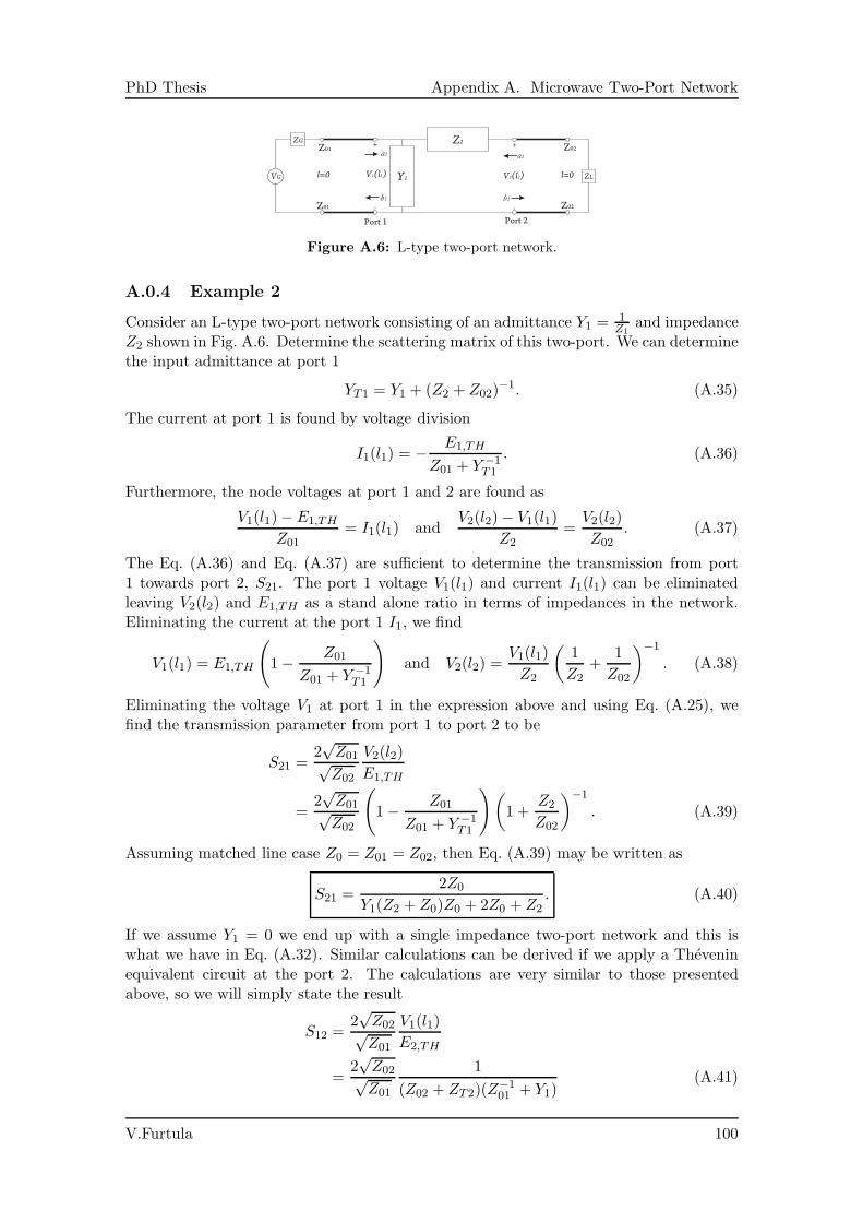
PhD Thesis Appendix A. Microwave Two-Port Network
ZG
VG ZLY1
Z2
V (l )1 1
+
-
a1
b1
+
b2
a2
-
V (l )2 2l=0 l=0
Port 1 Port 2
Z01
Z01
Z02
Z02
Figure A.6: L-type two-port network.
A.0.4 Example 2
Consider an L-type two-port network consisting of an admittance Y1 =1Z1
and impedanceZ2 shown in Fig. A.6. Determine the scattering matrix of this two-port. We can determinethe input admittance at port 1
YT1 = Y1 + (Z2 + Z02)−1. (A.35)
The current at port 1 is found by voltage division
I1(l1) = − E1,TH
Z01 + Y −1T1
. (A.36)
Furthermore, the node voltages at port 1 and 2 are found as
V1(l1)− E1,TH
Z01= I1(l1) and
V2(l2)− V1(l1)
Z2=V2(l2)
Z02. (A.37)
The Eq. (A.36) and Eq. (A.37) are sufficient to determine the transmission from port1 towards port 2, S21. The port 1 voltage V1(l1) and current I1(l1) can be eliminatedleaving V2(l2) and E1,TH as a stand alone ratio in terms of impedances in the network.Eliminating the current at the port 1 I1, we find
V1(l1) = E1,TH
(
1− Z01
Z01 + Y −1T1
)
and V2(l2) =V1(l1)
Z2
(
1
Z2+
1
Z02
)
−1
. (A.38)
Eliminating the voltage V1 at port 1 in the expression above and using Eq. (A.25), wefind the transmission parameter from port 1 to port 2 to be
S21 =2√Z01√Z02
V2(l2)
E1,TH
=2√Z01√Z02
(
1− Z01
Z01 + Y −1T1
)
(
1 +Z2
Z02
)
−1
. (A.39)
Assuming matched line case Z0 = Z01 = Z02, then Eq. (A.39) may be written as
S21 =2Z0
Y1(Z2 + Z0)Z0 + 2Z0 + Z2. (A.40)
If we assume Y1 = 0 we end up with a single impedance two-port network and this iswhat we have in Eq. (A.32). Similar calculations can be derived if we apply a Theveninequivalent circuit at the port 2. The calculations are very similar to those presentedabove, so we will simply state the result
S12 =2√Z02√Z01
V1(l1)
E2,TH
=2√Z02√Z01
1
(Z02 + ZT2)(Z−101 + Y1)
(A.41)
V.Furtula 100
PhD Thesis Appendix A. Microwave Two-Port Network
where ZT2 = Z2+(Z−101 +Y1)
−1 is the impedance seen from the port 2. Assuming matchedtransmission lines at input and output Z0 = Z01 = Z02, we find that
S21 =2Z0
2Z0 + Z2 + Y1Z0(Z2 + Z0). (A.42)
Note that S12 = S21 which tells us that the circuit is reciprocal. This is a fundamentalproperty for all passive circuits not containing any external sources or ferromagneticmaterials. The reflection loss at the input S11 is calculated using Eq. (A.23)
S11 =ZT1 − Z01
ZT1 + Z01
=(Y1 + (Z2 + Z02)
−1)−1 − Z01
(Y1 + (Z2 + Z02)−1)−1 + Z01(A.43)
Again, assuming matched line case Z0 = Z01 = Z02, Eq. (A.43) becomes
S11 =Z2 − Z0Y1(Z2 + Z0)
Z2 + 2Z0 + Z0Y1(Z2 + Z0). (A.44)
If we assume Y1 = 0 we find a single component two-port network we expressed inEq. (A.30). Similarly, the reflection at the port 2 can be found from Eq. (A.26)
S22 =ZT2 − Z02
ZT2 + Z02
=Z2 + (Z−1
01 + Y1)−1 − Z02
Z2 + (Z−101 + Y1)−1 + Z02
(A.45)
Assuming matched line case, the Eq. (A.45) becomes
S22 =Z2 + Z0Y1(Z2 − Z0)
Z2 + 2Z0 + Z0Y1(Z2 + Z0). (A.46)
If we make a similar evaluation for S11 by assuming Y1 = 0, we will find identical reflectionsat both ports. Another way to confirm our calculation is to assume Z2 = 0. Then we find
S11|Z2=0 = S22|Z2=0 =−Z0Y12 + Z0Y1
. (A.47)
This result is also what could be expected due to symmetry when Z2 is neglected. Noticethat the S-parameters S11 and S22 are in general different in both amplitude and phaseregardless of the circuit being lossless or not. Only symmetrical circuits can fulfill S11 =S22. The results in the boxed equations are convenient to memorize for general circuitanalysis using S-parameters.
Further in this thesis the terms such as Insertion Loss and Return Loss are used.These terms are closely related to the S-parameters, so they are introduced in the followingsection.
The insertion loss of a two-port network is defined as[65, p.170]
IL ≡ 10 logPLb
PLa
[dB], (A.48)
V.Furtula 101

PhD Thesis Appendix A. Microwave Two-Port Network
where PLb is the power delivered to a specified load (ZL) before inserting the network andPLa is the power delivered to the same load after inserting the network. In terms of theS-parameters insertion loss becomes
IL = 10 log|(1 − S11ΓG)(1− S22ΓL)− S12S21ΓGΓL|2|S21|2|1− ΓGΓL|2
(A.49)
Similarly, return loss is defined by the Eq. (A.7)
RL ≡ 10 logP+
P−= 10 log
1
|Γ|2 [dB]. (A.50)
At the input of a two-port network we have Γ = Γin and at the output we have Γ = Γout.The return loss at the input and output ports are found to be[65, p.170]
RLin = log|S11 +S12S21ΓL
1− S22ΓL|−2 and RLout = log|S22 +
S12S21ΓG
1− S11ΓG|−2. (A.51)
Assuming perfect match at the input and output, i.e. ΓG = 0 and ΓL = 0, the insertionloss becomes
IL = 10 log1
|S21|2= −20 log |S21|. (A.52)
For the same conditions |S12|2 represents reverse insertion loss and is found by placingthe load at the input and source at the output.Similarly, assuming perfect match at both ports return loss becomes
RLin = log|S11|−2 = −20 log |S11| and (A.53)
RLout = log|S22|−2 = −20 log |S22|. (A.54)
For pure passive circuits the insertion loss is symmetrical (S21 = S12) if all the ports areperfectly matched. This is not necessarily the case for return loss, but the symmetry canbe achieved (S11 = S22) if electrical properties of the two-port circuit are symmetrical.This has already been discussed in the two previous examples.
V.Furtula 102
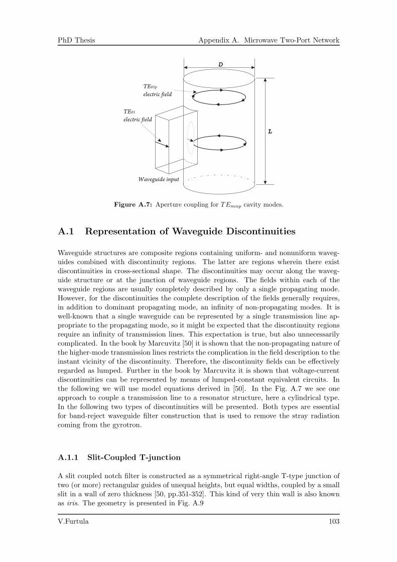
PhD Thesis Appendix A. Microwave Two-Port Network
D
L
Waveguide input
TE
electric field
01p
TE
electric field
01
Figure A.7: Aperture coupling for TEmnp cavity modes.
A.1 Representation of Waveguide Discontinuities
Waveguide structures are composite regions containing uniform- and nonuniform waveg-uides combined with discontinuity regions. The latter are regions wherein there existdiscontinuities in cross-sectional shape. The discontinuities may occur along the waveg-uide structure or at the junction of waveguide regions. The fields within each of thewaveguide regions are usually completely described by only a single propagating mode.However, for the discontinuities the complete description of the fields generally requires,in addition to dominant propagating mode, an infinity of non-propagating modes. It iswell-known that a single waveguide can be represented by a single transmission line ap-propriate to the propagating mode, so it might be expected that the discontinuity regionsrequire an infinity of transmission lines. This expectation is true, but also unnecessarilycomplicated. In the book by Marcuvitz [50] it is shown that the non-propagating nature ofthe higher-mode transmission lines restricts the complication in the field description to theinstant vicinity of the discontinuity. Therefore, the discontinuity fields can be effectivelyregarded as lumped. Further in the book by Marcuvitz it is shown that voltage-currentdiscontinuities can be represented by means of lumped-constant equivalent circuits. Inthe following we will use model equations derived in [50]. In the Fig. A.7 we see oneapproach to couple a transmission line to a resonator structure, here a cylindrical type.In the following two types of discontinuities will be presented. Both types are essentialfor band-reject waveguide filter construction that is used to remove the stray radiationcoming from the gyrotron.
A.1.1 Slit-Coupled T-junction
A slit coupled notch filter is constructed as a symmetrical right-angle T-type junction oftwo (or more) rectangular guides of unequal heights, but equal widths, coupled by a smallslit in a wall of zero thickness [50, pp.351-352]. This kind of very thin wall is also knownas iris. The geometry is presented in Fig. A.9
V.Furtula 103

PhD Thesis Appendix A. Microwave Two-Port Network
-jBa -jBa
-jBb
T
T’
Y0 Y0
Y’0
-jBa
T
T’
Y0
Y’0
-jBa -jBa
-jBb
T T
T’
Y0 Y0
Y’0
-jBa -jBa
-jBb
T
T’
Y0 Y0
Y’0
short short short
-jBa -jBa
-jBb
T
T’
Y0 Y0
Y’0
-jBa
T
T’
Y0
Y’0
short
ZG
VG ZL
TT
Y0
T
Y0
Figure A.8: The equivalent electrical circuit for a 4 pole Band-reject filter.
b
b’
a’
d
E
The main waveguide
The notch
waveguide
Iris opening
E
T
T’ b-jBa -jBa
jBb
T T
T’
Y0 Y0
Y’0
b’
d
E
(a) General view (c) Eqivalent circuit(b) Side view
Figure A.9: The capacitive slit coupling mechanism.
Ba
Y0=
bλg
(
πd4b
)2
1 + 16
(
πd4b
)2
(
bb′
)2+ 1
2 + 6
[
1−√
1−(
2bλg
)2]
+ 12(
bb′
)2
1√
1−
(
2b′
λg
)2− 1
(A.55)
Ba
Y0≈ b
λg
(
πd
4b
)2
, d≪ b, (A.56)
The guide wavelength λg of the rectangular waveguide is given as
λg =λ
√
1−(
λ2a
)2, (A.57)
where a is the waveguide width, so that a > b. Similarly, for Bb we have
Bb
Y0− Ba
2Y0=
4b
λg
ln2√2bb′
πd+
1
2
∞∑
n=1
1√
n2 −(
2bλg
)2− 1
n
, (A.58)
Bb
Y0≈ 4b
λg
[
ln2√2bb′
πd+
(
b
λg
)2]
, b≪ λg (A.59)
The restrictions using the results shown above is that equivalent circuit is applicable inthe wavelength range 2b/λg < 1 provided the slit dimension d is small compared withthe wavelength. All the equivalent circuit parameters are derived by an integral equationmethod.
V.Furtula 104
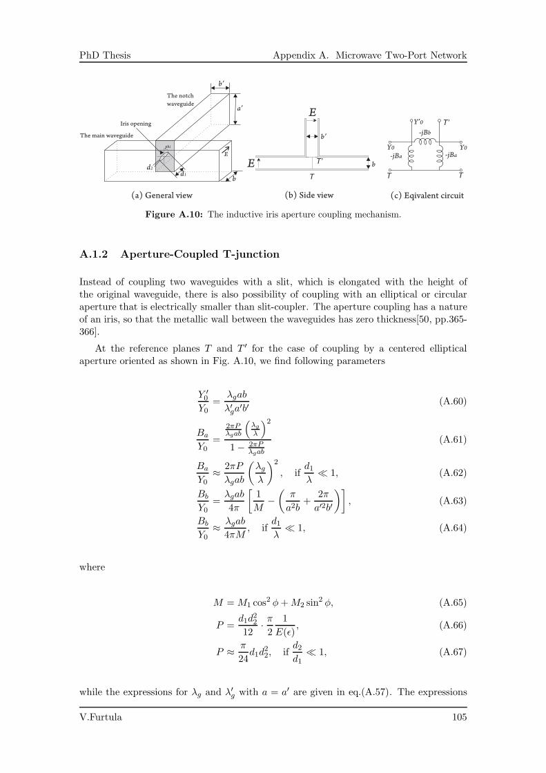
PhD Thesis Appendix A. Microwave Two-Port Network
b’
a’
d1
E
The main waveguide
The notch
waveguide
Iris opening
d2
phi
E
ET
T’ b-jBa -jBa
-jBb
T T
T’
Y0 Y0
Y’0
b
b’
(a) General view (c) Eqivalent circuit(b) Side view
Figure A.10: The inductive iris aperture coupling mechanism.
A.1.2 Aperture-Coupled T-junction
Instead of coupling two waveguides with a slit, which is elongated with the height ofthe original waveguide, there is also possibility of coupling with an elliptical or circularaperture that is electrically smaller than slit-coupler. The aperture coupling has a natureof an iris, so that the metallic wall between the waveguides has zero thickness[50, pp.365-366].
At the reference planes T and T ′ for the case of coupling by a centered ellipticalaperture oriented as shown in Fig. A.10, we find following parameters
Y ′
0
Y0=
λgab
λ′ga′b′
(A.60)
Ba
Y0=
2πPλgab
(
λg
λ
)2
1− 2πPλgab
(A.61)
Ba
Y0≈ 2πP
λgab
(
λgλ
)2
, ifd1λ
≪ 1, (A.62)
Bb
Y0=λgab
4π
[
1
M−(
π
a2b+
2π
a′2b′
)]
, (A.63)
Bb
Y0≈ λgab
4πM, if
d1λ
≪ 1, (A.64)
where
M =M1 cos2 φ+M2 sin
2 φ, (A.65)
P =d1d
22
12· π2
1
E(ǫ), (A.66)
P ≈ π
24d1d
22, if
d2d1
≪ 1, (A.67)
while the expressions for λg and λ′g with a = a′ are given in eq.(A.57). The expressions
V.Furtula 105
PhD Thesis Appendix A. Microwave Two-Port Network
for M1 and M2 are defined by
M1 =d316
π
4
ǫ2
F (ǫ)− E(ǫ), (A.68)
M2 =d1d
22
6
π
4
ǫ2
E(ǫ)− (1− ǫ2)F (ǫ)(A.69)
ǫ =
√
1−(
d2d1
)2
, (A.70)
and F (ǫ) and E(ǫ) are complete elliptic integrals of the first and second kinds, respectively.For the special case of a circular aperture d1 = d2 = d we have from (A.65) and (A.66)
M =d3
6and P =
d3
12. (A.71)
The equations describing both coupling methods have some restrictions too. In the small-aperture range d1/λ≪ 1 the equivalent circuit of Fig. A.9 is applicable at wavelengths forwhich only a single dominant H10-mode can be propagated in both waveguides. Also, itshould be emphasized that the above results apply to apertures in walls of zero thickness.For any waveguide coupling mechanism the maximum aperture dimension should be halfcompared to the guide wavelength λg.
V.Furtula 106
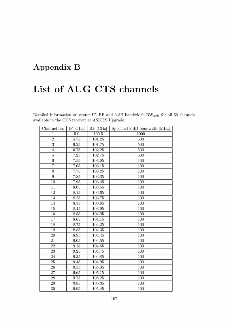
Appendix B
List of AUG CTS channels
Detailed information on center IF, RF and 3-dB bandwidth BW3dB for all 50 channelsavailable in the CTS receiver at ASDEX Upgrade.
Channel no. IF [GHz] RF [GHz] Specified 3-dB bandwidh [MHz]
1 5.0 100.5 1000
2 5.75 101.25 500
3 6.25 101.75 500
4 6.75 102.25 500
5 7.25 102.75 500
6 7.55 103.05 100
7 7.65 103.15 100
8 7.75 103.25 100
9 7.85 103.35 100
10 7.95 103.45 100
11 8.05 103.55 100
12 8.15 103.65 100
13 8.25 103.75 100
14 8.35 103.85 100
15 8.45 103.95 100
16 8.55 104.05 100
17 8.65 104.15 100
18 8.75 104.25 100
19 8.85 104.35 100
20 8.95 104.45 100
21 9.05 104.55 100
22 9.15 104.65 100
23 9.25 104.75 100
24 9.35 104.85 100
25 9.45 104.95 100
26 9.55 105.05 100
27 9.65 105.15 100
28 9.75 105.25 100
29 9.85 105.35 100
30 9.95 105.45 100
107

PhD Thesis Appendix B. List of AUG CTS channels
Channel no. IF [GHz] RF [GHz] Specified 3-dB bandwidth [MHz]
31 10.05 105.55 100
32 10.15 105.65 100
33 10.25 105.75 100
34 10.35 105.85 100
35 10.45 105.95 100
36 10.55 106.05 100
37 10.65 106.15 100
38 10.75 106.25 100
39 10.85 106.35 100
40 10.95 106.45 100
41 11.05 106.55 100
42 11.15 106.65 100
43 11.25 106.75 100
44 11.35 106.85 100
45 11.45 106.95 100
46 11.75 107.25 500
47 12.25 107.75 500
48 12.75 108.25 500
49 13.25 108.75 500
50 14.0 109.50 1000
V.Furtula 108
Bibliography
[1] C. A. BALANIS. Advanced Engineering Electromagnetics. John Wiley & Sons, 111River Street, Hoboken, NJ 07030, 1989.
[2] C. A. BALANIS. Antenna Theory. John Wiley & Sons, 111 River Street, Hoboken,NJ 07030, 3 edition, 2005.
[3] R. BEHN et al. Ion temperature-measurement of tokamak plasmas by collectiveThomson scattering of d2o laser-radiation. Phys. Rev. Lett., 62:2833–2836, 1989.
[4] H. A. BETHE. Lumped constants for small irises. M.I.T. Radiation Laboratory,Cambridge, Massachusetts, Report 43-22, 1943.
[5] H. BINDSLEV. Three wave mixing and thomson scattering in plasmas. PlasmaPhys. Control. Fusion, 35:1615–1640, 1993.
[6] H. BINDSLEV et al. Fast-ion velocity distributions in JET measured by collectiveThomson scattering. Phys. Rev. Lett., 83:3206–3209, 1999.
[7] H. BINDSLEV et al. Feasibility study of fast ion diagnosis in ITER by collectiveThomson scattering millimeter waves to co2 laser. Rev. Sci. Instrum., 75:3598–3600,2004.
[8] H. BINDSLEV et al. Fast-ion dynamics in TEXTOR measured by collective Thom-son scattering. Phys. Rev. Lett., 97:205005, 2006.
[9] A. A. BOGDASHOV, G. G. DENISOV, D. A. LUKOVNIKOV, Y. V. RODIN, andA. N. PANIN. Resonant notch filters based on rectangular waveguide extensions.Int. J. Infrared Millimeter Waves, pages 1029–1032, 2002.
[10] T. J. M. BOYD and J. J. SANDERSON. The Physics of Plasmas. CambridgeUniversity Press, The Edinburgh Building, Cambridge CB2 8RU, UK, 2005.
[11] Kai CHANG. Handbook of Microwave and Optical Components, volume 1. JohnWiley & Sons, Brooklyn, N.Y., 1989.
[12] E. M. CHOI et al. Megawatt power level 120 GHz gyrotrons for ITER start-up. J.Phys.: Conf. Series, 25(1):1, 2005.
[13] A.E. COSTLEY et al. Measurement requirements and the diagnostic system on iter:Modifications following the design review. Proc. 22nd IAEA Conf., 2008.
[14] E. de la LUNA and JET-EFDA contributors. Physics of ECE temperature mea-surements and prospects for ITER. In An International Conference on BURNINGPLASMA DIAGNOSTICS, pages 63–72. American Institute of Physics, September2007.
109
PhD Thesis Bibliography
[15] G. G. DENISOV, A. A. BOGDASHOV, A. N. PANIN, and YU. V. RODIN. Designand test of new millimeter wave notch filter for plasma diagnostics. In 33rd Inter-national Conference on Infrared, Millimeter and Terahertz Waves, pages 1–2. Int. J.Infrared Millimeter Waves, September 2008.
[16] G. G. DENISOV, S. V. KUZIKOV, and D. A. LUKONIKOV. Simple millimeter-wavenotch filters based on rectangular wave-guide extensions. Int. J. Infrared MillimeterWaves, 16(7):1231–1238, 1995.
[17] G. G. DENISOV, S. V. KUZIKOV, and M. Y. SHMELYOV. Quasi-optical narrow-band notch filters. Int. J. Infrared Millimeter Waves, 2104:353–354, 1993.
[18] G. G. DENISOV et al. Millimeter wave multi-mode transmission line components.Int. J. Infrared Millimeter Waves, 32(3):343–357, 2011.
[19] N.J. DOBBE et al. Control and RF-transmission in the ECW system on TEXTOR-94. Fusion Eng. Des., 56-57:599–604, 2001.
[20] YU. DRYAGIN, N. SCALYGA, and T. GEIST. A notch filter for 140 GHz microwaveradiation. Int. J. Infrared Millimeter Waves, 17(7):1199–1204, 1996.
[21] J. EGEDAL, H. BINDSLEV, R.V. BUDNEY, and P. WOSKOV. Impact of beamions on alpha-particle measurements by collective Thomson scattering in ITER. Nucl.Fusion, 45(3):191–200, 2005.
[22] K. FELCH et al. Recent ITER-relevant gyrotron tests. In Third IAEA TechnicalMeeting on ECRH Physics and Technology in ITER, pages 13–23. J. Phys.: Conf.Series, May 2005.
[23] V. FURTULA et al. Broadband notch filter design for millimeter-wave plasma diag-nostics. Rev. Sci. Instrum., 81:10D913, 2010.
[24] V. FURTULA et al. 105 GHz notch filter design for collective Thomson scattering.Fusion Sci. Tech., 59:670–677, 2011.
[25] V. FURTULA et al. Design and performance of the collective thomson scatteringreceiver at ASDEX Upgrade. Rev. Sci. Instrum., 83:013507, 2012.
[26] T. GEIST and M. BERGBAUER. Waveguide band-stop filters for 70 and 140 GHz.Int. J. Infrared Millimeter Waves, 15(12):2043–2049, 1994.
[27] P. F. GOLDSMITH and H. SCHLOSSBERG. A quasi-optical single sideband filteremploying a semiconfocal resonator. IEEE Transactions on Microwave Theory andTechniques, 28(10):1136–1139, 1980.
[28] V. L. GRANATSTEIN and I. ALEXEFF. High-Power Microwave Sources. ArtechHouse, Norwood, MA 02062, 1987.
[29] J. P. GRAVES et al. Control of magnetohydrodynamic stability by phase spaceengineering of energetic ions in tokamak plasmas. Nature Communications, 3(624),2012.
[30] A. GUDE, S. GUNTER, S. SESNIC, and ASDEX Upgrade Team. Seed island ofneoclassical tearing modes at ASDEX Upgrade. Nucl. Fusion, 39(1):127, 1999.
V.Furtula 110
PhD Thesis Bibliography
[31] STEN E. GUNNARSSON. Mixers and Multifunctional MMICs for Millimeter-WaveApplications. PhD thesis, Chalmers University of Technology, Gothenburg, Sweden,2008.
[32] S. GUNTER et al. and the ASDEX Upgrade Team. Neoclassical tearing modeson ASDEX Upgrade: improved scaling laws, high confinement at high βN and newstabilization experiments. Nucl. Fusion, 43(3):161, 2003.
[33] H. J. HARTFUSS, T. GEIST, and M. HIRSCH. Heterodyne methods in millimetrewave plasma diagnostics with applications to ECE, interferometry and reflectometry.Plasma Phys. Control. Fusion, 39(11):1693–1769, 1997.
[34] D. van HOUTTE et al. Recent fully non-inductive operation results in Tore Suprawith 6 min, 1 GJ plasma discharges. Nucl. Fusion, 44(5):L11–L15, 2004.
[35] Heating ITER Physics Expert Group on Energetic Particles and Current Drive. ITERphysics basis, ch. 5: Physics of energetic ions. Nucl. Fusion, 39(12):2471–2495, 1999.
[36] T. K. JOHANSEN and V. KROZER. Analysis and design of lumped element marc-hand baluns. In 17th International Conference on Microwaves, Radar and WirelessCommunications (MIKON), pages 1–4. IEEE Micr., Radar and Wireless Com., May2008.
[37] T. K. JOHANSEN et al. A high conversion-gain Q-Band InP DHBT subharmonicmixer using LO frequency doubler. IEEE Trans. on Micr. Th. and Tech., 56(3):613–619, 2008.
[38] A. KASUGAI et al. Steady-state operation of 170 GHz 1 MW gyrotron for ITER.Nucl. Fusion, 48(5):054009, 2008.
[39] S. B. KORSHOLM et al. Fast ion collective Thomson scattering diagnostic for ITER -progress of design. In BURNING PLASMA DIAGNOSTICS: An International Con-ference, September 2007, pages 118–122. American Institute of Physics, September2007.
[40] S. B. KORSHOLM et al. Collective Thomson scattering capabilities to diagnosefusion plasmas. Nucl. Instr. and Methods in Phys. Res., 623:677–680, 2010.
[41] S. B. KORSHOLM et al. Measurements of intrinsic ion Bernstein waves in a tokamakby collective Thomson scattering. Phys. Rev. Lett., 106:165004, 2011.
[42] S. B. KORSHOLM et al. Current fast ion collective Thomson scattering diag-nostics at TEXTOR and ASDEX Upgrade, and ITER plans. Rev. Sci. Instrum.,77(10):10E514, 2006.
[43] A. KRAMER-FLECKEN, W. PYSIK, and G. CZYMEK. 110 GHz notch-filter de-velopment at TEXTOR-94. Fusion Eng. Des., 56-57:639–643, 2001.
[44] S. KUBO et al. Collective Thomson scattering of a high power electron cyclotronresonance heating beam in LHD (invited). Rev. Sci. Instrum., 81:10D535, 2010.
[45] THOMAS H. LEE. The Design of CMOS Radio-Frequency Integrated Circuits. Cam-bridge, University Press, The Pitt Building, Trumpington Street, Cambridge, UK,2004.
V.Furtula 111
PhD Thesis Bibliography
[46] F. LEIPOLD et al. Antenna design for fast ion collective Thomson scattering diag-nostic for the international thermonuclear experimental reactor. Rev. Sci. Instrum.,80:093501, 2009.
[47] F. LEUTERER et al. Status of the new ECRH system for ASDEX upgrade. FusionEng. Des., 74:199203, 2005.
[48] N. C. LUHMANN et al. Microwave diagnostics. Fusion Sci. Tech., 53(2):335–396,2008.
[49] S. A. MAAS. Nonlinear Microwave and RF Circuits. Artech House, Inc., Norwood,MA 02062, 2003.
[50] N. MARCUVITZ. Waveguide Handbook. Peter Peregrinus Ltd., London, UK, Brook-lyn, N.Y., 1986.
[51] G. MATTHAEI, L. YOUNG, and E. M. T. JONES. Microwave Filters, Impedance-Matching Networks, and Coupling Structures. Artech House, 685 Canton Street,Norwood, MA 02062, 1980.
[52] F. MEO et al. Design of the collective Thomson scattering diagnostic for interna-tional thermonuclear experimental reactor at the 60 GHz frequency range. Rev. Sci.Instrum., 75:3585–3588, 2004.
[53] F. MEO et al. Commissioning activities and first results from the collective Thomsonscattering diagnostic on ASDEX Upgrade. Rev. Sci. Instrum., 79:10E501, 2008.
[54] F. MEO et al. First results and analysis of collective Thomson scattering (CTS)fast ion distribution measurements on ASDEX Upgrade. J. Phys.: Conf. Series,227(1):012010, 2010.
[55] D. MOSEEV et al. Comparison of measured and simulated fast ion velocity distri-butions in the TEXTOR tokamak. Plasma Phys. Control. Fusion, 53(10):105004,2011.
[56] S. K. NIELSEN. Fast ion dynamics in TEXTOR plasmas measured by means ofcollective Thomson scattering (CTS). PhD thesis, Forskningscenter Risø, TechnicalUniversity of Denmark, August 2007.
[57] S. K. NIELSEN et al. Temporal evolution of confined fast ion velocity distributionsmeasured by collective Thomson scattering in TEXTOR. Phys. Rev. E, 77:016407,2008.
[58] S. K. NIELSEN et al. Fast-ion redistribution due to sawtooth crash in the TEXTORtokamak measured by collective Thomson scattering. Plasma Phys. Control. Fusion,52:092001, 2010.
[59] S. K. NIELSEN et al. Dynamics of fast ions during sawtooth oscillations in theTEXTOR tokamak measured by collective Thomson scattering. Nucl. Fusion,51(6):063014, 2011.
[60] G. S. NUSINOVICH. Introduction to the Physics of Gyrotrons. The John HopkinsUniversity Press, 2004.
V.Furtula 112
PhD Thesis Bibliography
[61] J. ONGENA and G. van OOST. Energy for future centuries - prospects for fusionpower as a future energy source. Fusion Sci. Tech., 49(2T):3–15, 2006.
[62] F.P. ORSITTO et al. Requirements for fast particle measurements on ITER andcandidate measurement techniques. Nucl. Fusion, 47(9):1311–1317, 2007.
[63] G. PEREZ, T. ESTRADA, G. VAYAKIS, and C. WALKER. Thermal and mechani-cal analysis of the ITER plasma-position reflectometry antennas. In Proceeding of the25th Symposium on Fusion Technology (SOFT-25), pages 1488–1494. Fusion Eng.Des., June 2009.
[64] B. PIOSCZYK et al. Towards a 2 mw, cw, 170 GHz coaxial cavity gyrotron forITER. In 22nd Symposium on Fusion Technology, pages 481–485. Fusion Eng. Des.,September 2003.
[65] P. A. RIZZI. Microwave Engineering - Passive Circuits. Prentice-Hall, Inc., Engle-wood Cliffs, New Jersey 07632, 1988.
[66] Bahaa E.A. SALEH and Malvin Carl TECH. Fundamentals of Photonics. JohnWiley & Sons, 1991.
[67] M. SALEWSKI et al. Comparison of collective Thomson scattering signals due tofast ions in ITER scenarios with fusion and auxiliary heating. Plasma Phys. Control.Fusion, 51(3):035006, 2009.
[68] M. SALEWSKI et al. Impact of ICRH on the measurement of fusion alphas bycollective Thomson scattering in ITER. Nucl. Fusion, 49(2):025006, 2009.
[69] M. SALEWSKI et al. Investigation of first mirror heating for the CTS diagnostic inITER. Rev. Sci. Instrum., 79:10E729, 2008.
[70] M. SALEWSKI et al. Comparison of fast ion collective Thomson scattering measure-ments at ASDEX Upgrade with numerical simulations. Nucl. Fusion, 50(3):035012,2010.
[71] M. SALEWSKI et al. On velocity space interrogation regions of fast-ion collectiveThomson scattering at ITER. Nucl. Fusion, 51(8):083014, 2011.
[72] E. E. SALPETER. Electron density fluctuations in a plasma. Phys. Rev., 120:1528–1535, 1960.
[73] S. A. SCHELKUNOFF. Theory of antennas of arbitrary size and shape. Inst. ofElectrical and Electronics Eng., 72:1165–1190, 1984.
[74] Z. SHEN et al. 2-d passive millimeter wave imaging system for plasma diagnostics.In Proceedings of Asia-Pacific Microwave Conference 2007, pages 116–119. IEEE,December 2007.
[75] N. SKOU. Microwave radiometer systems: design and analysis. Artech House, 685Canton Street, Norwood, 1989.
[76] M. STEJNER et al. Collective Thomson scattering measurements with high fre-quency resolution at TEXTOR. Rev. Sci. Instrum., 81:10D515, 2010.
V.Furtula 113
PhD Thesis Bibliography
[77] M. STEJNER et al. Measurements of plasma composition in the TEXTOR tokamakby collective Thomson scattering. Plasma Phys. Control. Fusion, 54(1):015008, 2012.
[78] E. V. SUVOROV et al. Ion temperature and beam-driven plasma waves from col-lective scattering of gyrotron radiation in W7-AS. Plasma Phys. Control. Fusion,37(11):1207–1213, 1995.
[79] E. V. SUVOROV et al. Collective Thomson scattering at W7-AS. Plasma Phys.Control. Fusion, 39(12B):B337–B351, 1997.
[80] U. TARTARI et al. Critical issues highlighted by collective Thomson scattering belowelectron cyclotron resonance in FTU. Nucl. Fusion, 46(11):928–940, 2006.
[81] U. TARTARI et al. Evolution of the millimeter-wave collective Thomson scatteringsystem of the high-field tokamak Frascati Tokamak Upgrade. Rev. Sci. Instrum.,78:043506, 2007.
[82] M. THUMM et al. MW gyrotron development for fusion plasma applications. PlasmaPhys. Control. Fusion, 45:A143A161, 2003.
[83] M. TIURI. Radio astronomy receivers. Inst. of Electrical and Electronics Eng.,12(7):930–938, December 1964.
[84] E. TSAKADZE et al. Fast ion collective thomson scattering diagnostic for ITER:Design elements. Fusion Sci. Tech., 53(1):69–76, January 2008.
[85] G. VAYAKIS et al. ECE diagnostics for rto/rc ITER. Fusion Eng. Des., 53(1-4):221–227, 2001.
[86] G. VAYAKIS et al. Status and prospects for mm-wave reflectometry in ITER. Nucl.Fusion, 46(9):S836, 2006.
[87] D. H. WAGNER et al. Commissioning of the second two-frequency gyrotron in thenew multi-frequency ECRH system for ASDEX upgrade. In Infrared and MillimeterWaves, 15th International Conference on Terahertz Electronics, September 2007.
[88] D. H. WAGNER et al. Present status of the new multifrequency ECRH system forASDEX Upgrade. IEEE Trans. Plasma Sci., 36(2):324–331, 2008.
[89] D. H. WAGNER et al. Status of the new multi-frequency ECRH system for ASDEXUpgrade. Nucl. Fusion, 48(5):054006, 2008.
[90] E. WESTERHOF et al. Electron cyclotron resonance heating on TEXTOR. Nucl.Fusion, 43(11):13711383, 2003.
[91] E. WESTERHOF et al. Strong scattering of high power millimeter waves in tokamakplasmas with tearing modes. Phys. Rev. Lett., 103:125001, 2009.
[92] P WOSKOBOINIKOW, W. J. MULLIGAN, and R. ERICKSEN. 385 mu-md2o laserlinewidth measurements to -60 db. IEEE Journal of Quantum Electronics, 19(1):4–7,1983.
[93] PAULWOSKOV. Notch filter options for ITER stray gyrotron radiation. Proceedingsof LAPD-13, 2007.
V.Furtula 114

PhD Thesis Bibliography
[94] P. WOSKOW et al. Frequency measurements of the gyrotrons used for collectiveThomson scattering diagnostics at TEXTOR and ASDEX upgrade. Rev. Sci. In-strum., 77:10E524, 2006.
[95] R. J. WYLDE. Millimetre-wave Gaussian beam-mode optics and corrugated feedhorns. IEE Proceedings-H (Microwaves, Optics and Antennas), 131:258–262, 1984.
[96] H. ZIRATH. High-frequency noise and current-voltage characteristics of mm-waveplatinum nn+ GaAs schottky barrier diodes. J. of App. Phys., 60(4):1399–1407,1986.
[97] H. ZOHM et al., ASDEX Upgrade Team, and ECRH Group. Experiments on neo-classical tearing mode stabilization by ECCD in ASDEX upgrade. Nucl. Fusion,39(5):577, 1999.
V.Furtula 115

DTU Physics
Fusion and Plasma Physics
Technical University of Denmark
DTU Risø Campus
Frederiksborgvej 399
PO Box 49
DK-4000 Roskilde
Denmark
Phone +45 4677 4500
Fax +45 4677 4565
www.fysik.dtu.dk