microphotonic silicon waveguide components · 2017-04-28 · waveguides, modulation of...
TRANSCRIPT
VTT PUBLICATIONS 553
Microphotonic silicon waveguide components
Timo Aalto VTT Information Technology
Dissertation for the degree of Doctor of Science in Technology to be presented with due permission of the Department of Electrical and Communications Engineering
for public examination and debate in Auditorium AS1 at Helsinki University of Technology (Espoo, Finland) on the 10th of December, 2004, at 12 o'clock noon.

ISBN 9513864227 (soft back ed.) ISSN 12350621 (soft back ed.)
ISBN 9513864235 (URL: http://www.vtt.fi/inf/pdf/) ISSN 14550849 (URL: http://www.vtt.fi/inf/pdf/)
Copyright © VTT 2004
JULKAISIJA UTGIVARE PUBLISHER
VTT, Vuorimiehentie 5, PL 2000, 02044 VTT puh. vaihde (09) 4561, faksi (09) 456 4374
VTT, Bergsmansvägen 5, PB 2000, 02044 VTT tel. växel (09) 4561, fax (09) 456 4374
VTT Technical Research Centre of Finland, Vuorimiehentie 5, P.O.Box 2000, FIN02044 VTT, Finland phone internat. + 358 9 4561, fax + 358 9 456 4374
VTT Tietotekniikka, Tietotie 3, PL 1208, 02044 VTT puh. vaihde (09) 4561, faksi (09) 456 7012
VTT Informationsteknik, Tietotie 3, PB 1208, 02044 VTT tel. växel (09) 4561, fax (09) 456 7012
VTT Information Technology, Tietotie 3, P.O.Box 1208, FIN02044 VTT, Finland phone internat. + 358 9 4561, fax + 358 9 456 7012
Technical editing Leena Ukskoski Otamedia Oy, Espoo 2004

Aalto, Timo. Microphotonic silicon waveguide components. Espoo 2004. VTT Publications 553.78 p. + app. 73 p.
Keywords silicon microphotonics, integrated optics, silicon-on-insulator waveguides, SOI waveguides, waveguide bends, thermo-optical switching, multi-step patterning, polarisation maintaining fibers, polarisation extinction ratio
Abstract This thesis describes the design, simulation, fabrication and characterisation of micro-photonic silicon waveguide components on silicon-on-insulator (SOI) substrates. The focus is on approximately 10 µm thick and single-moded (SM) silicon rib waveguides. In particular, simulation results are given for straight and bent Si waveguides, directional couplers (DCs), thermo-optically (TO) modulated Mach-Zehnder interferometers (MZI), and waveguide gratings. A new analytical SM condition for Si rib waveguides is pro-posed and the development of a new grating simulation algorithm is reported. The theo-retical part of the work also involves inventions relating to multi-step patterning of Si waveguides, modulation of interferometric devices, and measurement of polarisation axes from waveguides and polarisation maintaining (PM) fibers.
Clean room processing of waveguide chips is briefly described. Main process steps are photolithography, electron-beam lithography, thermal oxidation, oxide deposition, oxide dry etching and Si dry etching. Post-processing of the chips is also reported, including dicing, polishing, anti-reflection (AR) coating, fiber pigtailing and wire bonding. The development of fabrication processes for multi-step patterning, waveguide gratings and photonic crystal waveguides is reported, although the optical characterisation of devices based on these three processes is not included in the thesis.
Experimental results are given for Si rib waveguides with different thicknesses (H) and widths (W). The minimum fiber coupling loss with H = 9 µm was 1.3 dB/facet without an AR coating. The AR coating reduced the coupling loss by 0.70.8 dB/facet. Mini-mum propagation loss for a 114 cm long waveguide spiral with H = 9 µm and W = 7 µm was 0.13 dB/cm. With H = 9 µm, the birefringence varied from 0.00063 to <0.0001 depending on the cladding material, and the maximum polarisation extinction ratio for straight waveguides and directional couplers was >15 dB. Furthermore, fast modulation with 15 dB extinction ratio (ER) is reported for TO MZI switches by using both tradi-tional (10 kHz) and novel (167 kHz) modulation methods. Rise and fall times for single switching operations were pushed below 750 ns with 9 dB ER. The setups and methods used in measurements are described in detail, including a novel method for measuring the polarisation axes of waveguides and PM fibers.
3

Preface The work presented in this thesis was carried out during the years 19972004 at the Technical Research Centre of Finland (VTT) in Espoo, Finland. The name and the or-ganisational status of the author's research group have changed more than once during this time. Presently it is called the Photonics group and it belongs to the Microelectronics research area of VTT Information Technology.
Most of the research work was performed in HILA, ELEOPTO-OPTIMI, OKSIDI and SOIWAVE projects. I thank the Academy of Finland, the European Space Agency (ESA), Tekniikan Edistämissäätiö and VTT for funding these projects and enabling my research work.
I thank my supervisor and former group leader at VTT, Prof. Matti Leppihalme, for encouraging and supporting me in my work during all these years. My present group leader Päivi Heimala deserves special compliments for originally introducing me to this fascinating research field and for conducting most of the actual clean room fabrication in this work. I also wish to express my gratitude to the former and present leaders of the Microelectronics Centre, Dr. Jouni Heleskivi and Dr. Ilkka Suni, for their interest and support in my research.
All my coauthors in the eight original publications helped me to build a solid foundation for this thesis, which is highly appreciated. I am particularly grateful to Mikko Harjanne for his invaluable help in simulations, image processing, programming, and electronics construction, as well as for his comments on the manuscript, and for our fruitful discus-sions. The work of Markku Kapulainen and Kimmo Solehmainen in device characterisa-tion and clean-room fabrication, and their comments on the manuscript, is greatly ac-knowledged. The contributions from my former colleagues Sanna Yliniemi and Pekka Katila, and the collaborators from the University of Joensuu, are appreciated. I would also like to thank all my present and former colleagues at VTT for providing a pleasant working environment and for making numerous small contributions to my work.
I thank Dr. Ari Tervonen from Nokia Research Center and Dr. Jyrki Saarinen from Hep-tagon for carefully pre-examining the manuscript.
I thank all my friends and relatives for encouraging me in this work and for sometimes taking my thoughts out of this work. The latter applies particularly well to my two sons, Jaakko and Ville, with whom I wish to spend more time after the hectic finishing of the manuscript. Finally, I thank my beloved wife Maarit for standing besides me all these years and for her patience and support during this work.
Timo Aalto Espoo, November 14, 2004
4

Contents Abstract.............................................................................................................................3 Preface ..............................................................................................................................4 Contents ............................................................................................................................5 List of original publications ............................................................................................7 Author's contribution ......................................................................................................9 List of symbols and abbreviations ................................................................................11 1. Introduction.............................................................................................................15
1.1 Historical perspective.......................................................................................15 1.2 Silicon technology............................................................................................15 1.3 Silicon microphotonics.....................................................................................18 1.4 Silicon-on-insulator (SOI) waveguide technology...........................................21 1.5 Aims of the thesis.............................................................................................24 1.6 Organisation of the thesis.................................................................................24
2. Theory, simulation and design ...............................................................................25 2.1 Electromagnetic theory of waveguides ............................................................25 2.2 Straight waveguides .........................................................................................27 2.3 Optical coupling of fibers and silicon waveguides...........................................34 2.4 Bends and mirrors in Si waveguides ................................................................36 2.5 Directional couplers and interferometric switches ...........................................39 2.6 Multi-step patterning of silicon waveguides ....................................................43 2.7 Waveguide gratings..........................................................................................45 2.8 Polarisation cross-talk ......................................................................................46
3. Fabrication...............................................................................................................49 3.1 Clean-room processing.....................................................................................49 3.2 Post-processing and fiber pigtailing .................................................................52 3.3 Waveguide gratings and photonic crystal structures ........................................53
4. Experimental results ...............................................................................................55 4.1 Construction of the measurement set-ups ........................................................55 4.2 Optical coupling of fibers and silicon waveguides...........................................56 4.3 Propagation and bending losses of silicon waveguides....................................59 4.4 Polarisation characteristics of Si waveguides and directional couplers ...........61 4.5 Fast thermo-optic 2x2 MZI switch...................................................................63
5. Conclusions ..............................................................................................................67 References.......................................................................................................................69 Appendix A: Simulation tools Publications IVIII Appendices II, III and VII of this publication are not included in the PDF version. Please order the printed version to get the complete publication (http://www.vtt.fi/inf/pdf/)
5

6
List of original publications This thesis includes the following selection of publications, which are referred to in the text by Roman numerals IVIII and briefly described below. Additional unpublished data is also presented.
I T. Aalto, M. Harjanne, M. Kapulainen, P. Heimala, and M. Leppihalme, "Devel-opment of silicon-on-insulator waveguide technology", Photonics West 2004, San Jose, USA, 2629 January 2004. Proceedings of SPIE, Vol. 5355, pp. 8195, 2004.
II M. Harjanne, T. Aalto, "Design of tight bends in silicon-on-insulator ridge waveguides", Physica Scripta, Vol. T114, pp. 209212, 2004.
III T. Aalto, P. Heimala, and P. Katila, "Integrated optical switch based on SOI-technology", Physica Scripta, Vol. T79, pp. 123126, 1999.
IV T. Aalto, M. Kapulainen, S. Yliniemi, P. Heimala, and M. Leppihalme, "Fast thermo-optical switch based on SOI waveguides", Photonics West 2003, San Jose, USA, 2729 January, 2003. Proceedings of SPIE, Vol. 4987, pp. 149159, 2003.
V M. Harjanne, M. Kapulainen, T. Aalto, and P. Heimala, "Sub-µs switching time in silicon-on-insulator MachZehnder thermooptic switch", Photonics Technology Letters, Vol. 16, No. 9, pp. 20392041, 2004.
VI J. Tervo, M. Kuittinen, P. Vahimaa, J. Turunen, T. Aalto, P. Heimala, and M. Lep-pihalme, "Efficient Bragg waveguide-grating analysis by quasi-rigorous approach based on Redheffer's star product", Optics Communications, Vol. 198, pp. 265272, 2001.
VII P. Heimala, T. Aalto, S. Yliniemi, J. Simonen, M. Kuittinen, J. Turunen, and M. Leppihalme, "Fabrication of Bragg grating structures in silicon", Physica Scripta, Vol. T101, pp. 9295, 2002.
VIII T. Aalto, M. Harjanne, and M. Kapulainen, "Method for the rotational alignment of polarization-maintaining optical fibers and waveguides", Optical Engineering, Vol. 42, Issue 10, pp. 28612867, 2003.
7
Publication I covers the majority of the results obtained in the entire work. It starts with an introduction to slab-, strip-, and rib-types of Si waveguides, followed by simulation results for the single-mode limits and bending losses in rib waveguides. Experimental results are then given for the polarisation properties of rib waveguides and for thermo-optical switching. Finally, the multi-step patterning principle is proposed.
Publication II presents simulation results for bent Si rib waveguides with three thick-nesses and with an optional groove. The results demonstrate the ability to significantly reduce the bending radius by using smaller waveguides or additional grooves. Numerical S-bend optimisation is also described.
Publication III presents the design and simulation of a thermo-optical switch based on Si rib waveguides in a 2×2 MachZehnder interferometer layout. This early work led to a mask layout used to fabricate all the thermo-optical switches reported in this thesis.
Publication IV presents experimental results for the thermo-optical switch and introduces a novel modulation principle. Some introduction and background to optical switching is also given, and the switch fabrication is described in detail. Experimental results are presented for both traditional modulation (up to 10 kHz) and the new type of modulation (up to 167 kHz). Compromises of speed vs. power consumption are discussed.
Publication V presents the application of the novel modulation principle to the minimisa-tion of single rise- and fall-times in a thermo-optical switch. The new method and the im-proved control electronics are described. Results with the traditional (rise- and fall-times 2935 µs) and new modulation method (rise- and fall-times 0.70.73 µs) are given.
Publication VI introduces a computationally efficient, quasi-rigorous simulation method developed for the design of etched gratings on top of Si rib waveguides. Thorough de-scription of the new method and a comparison to a traditional film-stack method are given. The new method is particularly useful for analysing deep gratings and the cou-pling of light between different waveguide modes.
Publication VII describes the fabrication of Si rib waveguides and grating structures. The design and simulation of gratings are summarised and the fabrication of rib waveguides is described. Then the fabrication of gratings on Si substrates by using electron-beam lithography and dry etching is reported. Finally, the process combination and the realisa-tion of waveguide gratings and other nanostructures on top of waveguides is discussed.
Publication VIII introduces a novel method for measuring the rotational angle of a fiber's or a waveguide's polarisation axis. Alignment needs in polarisation maintaining (PM) optical systems, alternative methods and a detailed theory of the new method are de-scribed. Experimental results indicate an angular accuracy better than ±0.2°. The new method can be used e.g. to rotationally align PM fibers with respect to Si waveguides.
8

Author's contribution The results presented in this thesis were obtained in collaboration with several other persons from VTT, the Helsinki University of Technology and the University of Joen-suu. The author has written publications I, III, IV and VIII. He has participated actively in the writing of publications II and V, and somewhat in the writing of publications VIVII. The author has been responsible for the overall guidance of work reported in publi-cations III, IVV and VIII, and participated in the guidance of work reported in publi-cations III, VI and VII.
The author was responsible for the theory, simulation and design of all the waveguide components reported in publications I and IIIV. He carried out all the simulations for these publications by himself, except for the bend simulations in publication I. In publi-cation II, the author actively guided the work and participated in the writing of the paper, although most of the simulations were not carried out by him. He proposed the multi-step patterning of silicon waveguides (publications I and II). He invented the new modu-lation principle and the new rotational alignment method, which are described and dem-onstrated in publications I, IIIV, and VIII. He also designed all the lithographic masks (device layouts) used in the fabrication. In publications VIVII, the author defined the target structures for simulation and fabrication, calculated the effective indices, and analysed the validity of the new simulation tool for this work. In publication VIII the author was responsible for all theoretical aspects.
With respect to fabrication (publications I, IV, and VII), the author typically had a smaller role and was not responsible for the actual clean-room fabrication. Nevertheless, he usually defined the targets for waveguide structures and processes, and suggested several new processing methods. He had a central role in the development of waveguide grating processes (publication VII) and post-processing steps (dicing, polishing, AR-coating, and wire bonding).
The author had a significant role in all measurements (I and VIII) and thermo-optical switching experiments (publications IIIV). Many of them were actually carried out by others, but the author had a substantial impact in the guidance of all measurements, in the numerical post-processing of measured raw data, and particularly in the development of measurement and switching methods.
9

10

List of symbols and abbreviations c Speed of light in vacuum c1 Numerical variable for the proposed new SM limit (default -0.1) dAR Thickness of a single-layer antireflection coating E Electric field vector h Thickness of the silicon slab surrounding a rib H Waveguide thickness (total silicon thickness at the location of rib) H Magnetic field vector I Intensity of light n Refractive index of a material n0 Refractive index of waveguide cladding (usually 11.5, default 1.46) nAR Refractive index of a single-layer antireflection coating ngap Refractive index of a material in a gap between a fiber and a waveguide nSi Refractive index of silicon (3.48) N Number of propagating waveguide modes neff Effective index of a waveguide mode P Heating power (P1 and P2 for waveguides 1 and 2, respectively) or optical power (P1 and P2 for two orthogonal polarisations) PON Heating power needed for an ON state when only one heater is used Pbias Heating power used for both waveguides in a biased OFF state Q Correction term for the Soref's SM limit (QTE for TE and QTM for TM) r 1/e field radius of a gaussian field (r1 and r2 for fields 1 and 2, respectively) or ratio of real and ideal directional coupler length (for 50:50 operation) rSMF 1/e field radius of a SM fiber (default 5 µm) R Bending radius s Fraction of input power for a 2×2 MZI that is always divided equally to both
outputs e.g. due to scattering S Poynting vector TBAR Relative output power (or transmission for lossless operation) from the bar
port of a 2×2 MZI (i.e. 1-TCROSS) TCROSS Relative output power (or transmission for lossless operation) from the cross
port of a 2×2 MZI (TCROSS,min and TCROSS,max are the minimum and maximum when ∆φ is varied, TCROSS,ideal corresponds to an ideal directional coupler with r = 1, s = 0)
11

W Waveguide (rib) width W10 Proposed new width limit for eliminating higher order vertical modes in rib
waveguides WSM Proposed new width limit for SM rib waveguides WSoref Soref's width limit for thick SM rib waveguides WSoref,Q Soref's more accurate width limit for SM rib waveguides x Horizontal coordinate (along chip surface) y Vertical coordinate (perpendicular to chip surface) z Longitudinal coordinate (along waveguide axis) α Rotational angle (e.g. in a rotational junction or for a rotatable polariser) or deflection angle in a waveguide mirror ∆φ Phase difference between two waveguides or polarisation modes ∆n Refractive index difference between a waveguide core and its cladding ∆neff Effective index difference in a waveguide grating (groove vs. no groove) ∆ρ Radial misalignment in a fiber-waveguide junction ∆T Temperature difference between two waveguide branches ∆z Longitudinal misalignment in a fiber-waveguide junction ε Permittivity ε0 Vacuum permittivity η Coupling coefficient between two electro-magnetic fields κ Coupling coefficient in a fiber-waveguide junction when θρ = ∆ρ = 0 λ Wavelength in vacuum (default 1550 nm) µ Permeability µ0 Vacuum permeability θρ Angular misalignment in a fiber-waveguide junction (around ∆ρ) θx Angular misalignment in a fiber-waveguide junction (around x) θy Angular misalignment in a fiber-waveguide junction (around y) Ψ Arbitrary component of an electro-magnetic field 1D One-dimensional (2D and 3D for two- and three-dimensional) ALD Atomic layer deposition AR Anti-reflection AWG Arrayed waveguide grating BESOI Bond and etch-back SOI
12
BiCMOS Bipolar complementary metal oxide semiconductor BOX Buried oxide (between silicon substrate and silicon core) BPM Beam propagation method CVD Chemical vapour deposition CMOS Complementary metal oxide semiconductor DC Directional coupler Det. Detector DUT Device under test (sample) EDFA Erbium doped fiber amplifier EIM Effective index method ELTRAN Epitaxial layer transfer (SOI wafer) ER Extinction ratio (ratio of the two output powers from a 2×2 MZI) ERideal Extinction ratio for an ideal 2×2 MZI (assuming r = 1, s = 0) FDTD Finite difference time domain ICP Inductively coupled plasma IL Insertion loss JoFy Department of Physics at the University of Joensuu IC Integrated circuit IR Infrared LED Light emitting diode LTO Low temperature oxide LWC Line width change with respect to a nominal width on a mask MEMS Micro-electro-mechanical-system MM Multi-moded MMF Multi-moded fiber MMI Multi-mode interference MZI MachZehnder interferometer PDL Polarisation dependent loss PhC Photonic crystal PIC Photonic integrated circuit PM Polarisation maintaining PMD Polarisation mode dispersion PMF Polarisation maintaining fiber PXR Polarisation extinction ratio (PXRin and PXRout for input and output, respec-
tively)
13

RIE Reactive ion etching SEM Scanning electron microscope SIMOX Separation by implanted oxygen (SOI wafer) SM Single-moded SMF Single-mode fiber SOI Silicon-on-insulator TEOS Tetraethyl orthosilicate TIR Total internal reflection TE Transverse electric (E horizontally with respect to the Si chip) TEXY TE polarised waveguide mode with X+1 and Y+1 intensity maxima in the x-
and y-directions, respectively TM Transverse magnetic (E vertically with respect to the Si chip) TMXY TM polarised waveguide mode with X+1 and Y+1 intensity maxima in the x-
and y-directions, respectively TO Thermo-optical TOX Thermal oxide UV Ultraviolet
14

1. Introduction 1.1 Historical perspective
The entire technological history of mankind can be divided into four material eras. Each of them is associated with a certain material that people learned to find or fabricate, to process by different tools and methods, and to finally turn into useful products. The adoption of each material led to a significant technological progress. The first three eras were the Stone Age (2,000,0003000 BC), the Bronze Age (30001200 BC), and the Iron Age (1200 BC 1950 AD). The Industrial Revolution was the capstone of the Iron Age. The machines, tools, bridges, ships, trains, cars, airplanes etc. made from iron let us move easily from one place to another and provided us a multitude of new mechanical products for our everyday life. The huge leaps in fabrication technology that followed the introduction of iron, and its important derivative material, steel, have now mostly passed and we have entered a new era. The first impression might be that in our present information society the technology has become immaterial or that it is based on a variety of equally important materials. However, this is not the case.
The fourth and present era can be called the Silicon Age (1950). It started from the first silicon transistor demonstrations at around 1950 and it probably continues for at least two decades more. Silicon provided us the ability to build intelligent machines, supple-mented our own limited capacity for numerical calculations, and enabled us to commu-nicate easily with anybody and anywhere. The present time is sometimes also called the Communication Age or the Information Age. However, based on the central role of silicon in the overwhelmingly fast technological development during the past fifty years, as well as in the foreseeable future, it is quite reasonable to call it the Silicon Age.
1.2 Silicon technology
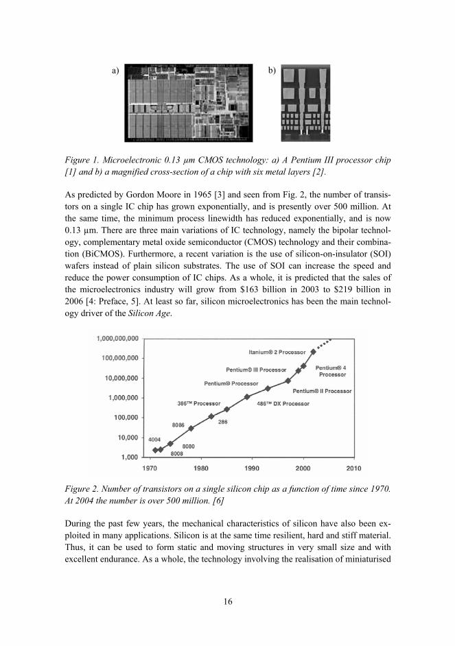
What makes silicon so special? So far, it has been its semiconductor character. Single-crystal silicon is a semiconductor by nature, but by oxidation and doping with impurity atoms (typically boron or phosphorus) one can radically change its electrical properties, in particular its resistivity. The amount and type of impurity atoms (n- or p-type) deter-mines the amount and type of free carriers (electrons or holes) that conduct electrical charges in silicon. Under the influence of an electric field, a deficiency of electrons, i.e. holes, can conduct charges just as well as a surplus of electrons. In a technology called Silicon Microelectronics, the ability to control the doping permits the formation of tran-sistors, diodes and resistors. By combining these fundamental building blocks in various ways it is possible to realise integrated circuits (ICs), the functional parts of silicon mi-crochips that exist inside almost every modern electronic product (see Fig. 1).
15
b) a)
Figure 1. Microelectronic 0.13 µm CMOS technology: a) A Pentium III processor chip [1] and b) a magnified cross-section of a chip with six metal layers [2].
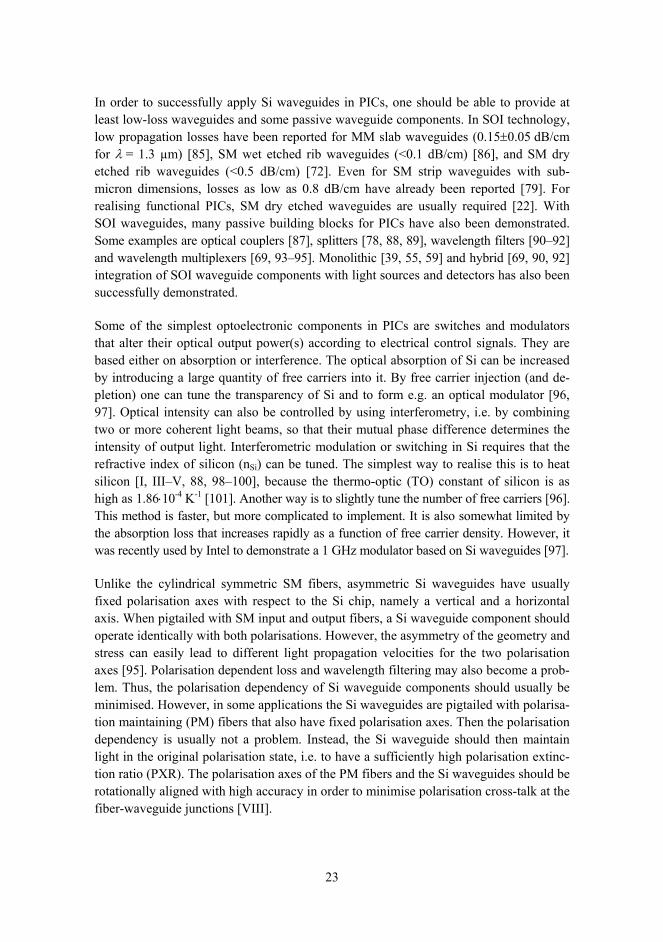
As predicted by Gordon Moore in 1965 [3] and seen from Fig. 2, the number of transis-tors on a single IC chip has grown exponentially, and is presently over 500 million. At the same time, the minimum process linewidth has reduced exponentially, and is now 0.13 µm. There are three main variations of IC technology, namely the bipolar technol-ogy, complementary metal oxide semiconductor (CMOS) technology and their combina-tion (BiCMOS). Furthermore, a recent variation is the use of silicon-on-insulator (SOI) wafers instead of plain silicon substrates. The use of SOI can increase the speed and reduce the power consumption of IC chips. As a whole, it is predicted that the sales of the microelectronics industry will grow from $163 billion in 2003 to $219 billion in 2006 [4: Preface, 5]. At least so far, silicon microelectronics has been the main technol-ogy driver of the Silicon Age.
Figure 2. Number of transistors on a single silicon chip as a function of time since 1970. At 2004 the number is over 500 million. [6]
During the past few years, the mechanical characteristics of silicon have also been ex-ploited in many applications. Silicon is at the same time resilient, hard and stiff material. Thus, it can be used to form static and moving structures in very small size and with excellent endurance. As a whole, the technology involving the realisation of miniaturised
16

beams, membranes, springs, resonators (see Fig. 3a), microfluidistic channels (see Fig. 3b), micromotors etc. in silicon, is called Silicon Micromechanics [712], also known as silicon micro-electro-mechanical-system (MEMS) technology. It has grown fast and it plays an important role in the miniaturisation and cost reduction of numerous products, such as oscillators, microphones, mobile phones, radios, scanners, ink jet printers, iner-tial sensors and diagnostic equipment for health care.
b) a)
Figure 3. Micromechanical silicon chips. a) SiC microresonator on Si [9]. b) Microflu-idic particle filter (etch depth ~0.5 mm) fabricated at VTT.
The third, and so far last, sector of silicon technology is called Silicon Microphotonics. It involves the realisation of optical functions on silicon chips (see Fig. 4) and it has been studied actively since the early 1990's. Much progress has been made, but the research efforts have been smaller than those in silicon micromechanics, and negligible compared to silicon microelectronics. Thus, silicon microphotonics is still in its infancy and has many technical challenges to tackle. Recent advancement has been very fast, which indicates a potential to solve the remaining problems and to commercialise the technol-ogy in larger scale. This makes silicon microphotonics a very attractive research subject.
Figure 4. A simple silicon microphotonic chip (~30×12 mm2) including three thermo-optic 2×2 switches, and a detail of a thin-film heater on top of a Si waveguide.
The success of silicon is not based only on its material characteristics, but on the combi-nation of its availability, cost, processability and compatibility with other materials. Raw silicon can be easily extracted from silica sand, which is readily available throughout our planet. With the help of a single-crystal seed, a large single-crystal Si rod can be slowly
17

pulled out of melted silicon. Desired type and amount of doping can be accurately ob-tained by adding impurities, such as phosphorus or boron, into the melted silicon. The cooled Si rod can be sawn and polished into wafers, which form the substrates for further processing. Typical wafers are 0.50.8 mm thick and 100 to 400 mm in diameter (416"). The realisation of microelectronic, micromechanical and microphotonic compo-nents on Si wafers is usually carried out in a clean room, i.e. in an ultra-clean facility. Typical processing steps are the deposition of metallic and dielectric thin films, litho-graphic patterning of photo-sensitive resist layers, ion implantation, diffusion of impurity atoms into silicon, thermal oxidation of Si to produce silicon dioxide (SiO2), wet etching with liquid chemicals and dry etching by ion bombardment. The strength of Si technol-ogy is that standard processes and tools are used to fabricate chips for numerous applica-tions in very large quantities and with excellent yield. Huge research and development efforts carried out during the past fifty years have made silicon microelectronics a ma-ture, reliable and cost-effective technology that has not been challenged by any other technology. Its continuing progress and recent roadmaps for IC technology indicate that this situation will remain at least for two decades more [5].
The development of silicon micromechanics and microphotonics has the clear advantage and justification in that it can use a mature microelectronics fabrication technology as a platform. Further on, it can extend the Silicon Age by offering new Si-based solutions for various non-electronic applications, and by enabling the unique opportunity of mono-lithic integration for microelectronics, micromechanics and microphotonics on a single chip. Some examples of attractive monolithic integration technologies are 1) optical clock distribution, signalling or computing carried out within a single Si chip [13], 2) integration of ICs to support microphotonic [14] and 3) micromechanical components [11], and 4) integration of optical waveguides or control electronics with microfluidic channels in optical diagnostics [15]. Further motivation for studying Si technologies can be found e.g. from recent review books written about silicon-based microfabrication [16], microelectronics [17], micromechanics [12] and microphotonics [4].
1.3 Silicon microphotonics
Silicon Microphotonics is a technology involving Si-based generation, conduction, ma-nipulation and detection of light in microscopic scale. As electrons and photons are the basic elements of electricity and light, it is the optical equivalent of silicon microelec-tronics. Electrons propagate along regions of high electrical conductivity, while photons propagate along regions of high refractive index. In silicon microphotonics, optical waveguides correspond to electrical wires, as they propagate light from one place to another. Similarly, photonic integrated circuits (PICs) correspond to electrical ICs. Some of the passive building blocks for PICs are optical couplers, splitters, wavelength filters and wavelength multiplexers. Optoelectronic components, such as lasers, light emitting diodes (LEDs), detectors, switches and modulators act as a bridge between optical and
18

electronic signals. Optical amplifiers can boost attenuated optical signals and, thus, com-pensate for the losses associated with non-ideal components and power splitters. If opti-cal transistors, wavelength converters and other all-optical components based on nonlin-ear phenomena will be successfully commercialised in the future, they may enable ex-tremely fast optical computing and all-optical, packed-switched fiber-networks.
In order to use the term silicon microphotonics, one must realise some key components onto silicon substrates. The direct fabrication of different components onto a common Si substrate is called monolithic integration. Correspondingly, the attachment of separate components (fibers, chips etc.) to Si devices is called hybrid integration [18]. Today, fast modulators, light sources, amplifiers, detectors and most other optoelectronic compo-nents can be made more efficient and low-cost by using other materials, such as lithium niobate [18: pages 920] or IIIV compound semiconductors [18: pp. 161238]. There-fore, their integration with Si PICs is presently easier with hybrid methods.
In hybrid integration and when attaching (pigtailing) optical fibers to Si chips, the optical coupling between optical sub-components is of significant importance, especially when dealing with single-moded (SM) optical systems, as was done in this thesis. Single-mode optics is much more sensitive to misalignments than electronics. Transverse and angular misalignments between two SM sub-components should preferably be kept below 1 µm and 1°, respectively. In SM hybrid products, the tedious assembly work dominates the overall costs and limits the commercialisation. Therefore, mass-production should be based on passive or automated alignment, or monolithic integration. For some applica-tions, such as short-range interconnections, multi-moded (MM) optics may also be used. Examples of hybrid integration are illustrated in Fig. 5.
b) Flip-chip bonded detector on a Si waveguide chip a) Fiber array on a
V-groove chip Si waveguide array on a Si chip
Figure 5. Examples of optical hybrid integration on silicon: a) fiber pigtailing of a Si waveguide array and b) flip-chip bonded detector on a Si chip.
Silicon microelectronics and micromechanics are not based on silicon alone, but they also involve many other materials, including various metals and dielectrics. Correspond-ingly, the fabrication and monolithic integration of photonic components on Si does not require that the components are made of silicon, but they may as well be made of sili-con-compatible materials added on top of a Si wafer. The rest of this chapter briefly
19

describes the main techniques used for photonic device fabrication and monolithic integration on silicon substrates.
Waveguides can be made of silicon itself, e.g. by using the SOI waveguide technology (see Chapter 1.4) or differently doped silicon layers [19, 20]. Even in the case of SOI waveguides, the silicon core (refractive index n = nSi ≈ 3.5) is typically surrounded by other materials, such as thermal oxide (TOX, SiO2, n ≈ 1.5). Several types of so-called glass waveguides have also been fabricated on silicon (and glass) substrates by doping SiO2 with impurity materials, such as As, B, Ge, N, P, Ti, or their combinations [15, 18, 2125]. Examples of other Si-compatible waveguide materials are e.g. silicon nitride (Si3N4, n ≈ 2) [2628] and polymers [18]. Different waveguide materials are favoured for different applications and wavelengths, because each material has its own advantages and drawbacks.
The realisation of light sources and optical amplifiers on Si substrates has been investi-gated by using surface-textured bulk silicon (wavelength λ < 1250 nm) [29], Si nano-crystals (λ < 1200 nm) [3032], erbium-doped Si [33] or SiOx (λ ≈ 1550 nm) [18, 34], the combination of Er and Si nanocrystals (λ ≈ 1550 nm) [35, 36], Si/SiGe quantum cascade structures (λ ≈ 7 µm) [37], Raman scattering (λ ≈ 1550 nm) [3840], and or-ganic materials (λ up to 1550 nm) [41, 42]. Several breakthroughs have been made dur-ing the last four years and Si nanocrystals have even indicated stimulated emission [30, 31, 43, 44], the necessity for a silicon laser. Wavelength conversion has also been dem-onstrated in Si by using stimulated Raman scattering [40, 45]. Despite the promising results, the Si-based generation, amplification and wavelength conversion of light are still the greatest challenges in silicon microphotonics. Especially at wavelengths around 1550 nm, an efficient and reliable Si-based transmitter is still to be developed.
Silicon-based photodetectors have also been studied by using different approaches. De-tectors for visible wavelengths can be fabricated from Si by using standard bipolar [14] and BiCMOS processes [4648], or by using modified processes [49, 50]. Fast (>2 Gb/s) operation has been demonstrated with good responsivity (0.11 A/W) and low voltage (2 V) [51]. A potential mass market for Si detectors at visible wavelengths is in optical disc drives [46]. For near-infrared (IR) detectors operating e.g. at λ = 13001550 nm, the material of choice is epitaxial germanium on silicon. Unlike Si, Ge absorbs IR light. It is also compatible with Si technology, although the 4% lattice mismatch between Si and Ge somewhat hinders their monolithic integration. For the fabrication of photodetectors on Si, germanium has been introduced as thin Ge layers [5254], Si/SiGe superlattices [5558] and Ge islands [55, 59, 60]. Some modest results have also been reported from Er-doped SOI waveguide detectors (λ ≈ 1550 nm) [61]. The latest results with Ge at λ ≈ 1550 nm have shown fast operation (>2 Gb/s), good responsivity (0.75 A/W) and low voltage (<1 V) [52], thus making monolithic near-IR detectors on Si already com-petitive with hybrid solutions.
20

1.4 Silicon-on-insulator (SOI) waveguide technology
In silicon microphotonics, silicon can be used not only as a substrate, but also as a wave-guide core material [IVII, 4, 6270]. The most straightforward way is to use silicon-on-insulator wafers, as was done in this work. They typically involve a thin SOI layer (i.e. a device layer) of single-crystal silicon on top of a Si substrate, with a thin buried oxide (BOX, SiO2) layer between them. SOI wafers are also used in microelectronics and mi-cromechanics, although the optimum resistivity and thickness of the SOI layer, as well as the optimum BOX thickness, often vary between different applications.
There are four main variations in the fabrication of commercial SOI wafers. So-called SIMOX (separation by implanted oxygen) wafers are based on oxygen implantation to plain Si wafers [71, 72]. They have SOI and BOX thicknesses <500 nm. This limits their applicability in microphotonics, although they are widely used in microelectronics [73]. In a so-called "Smart-Cut" process [71, 74], hydrogen ions are implanted to a plain Si wafer, which is then bonded to an oxidised Si wafer. The formed "zipper" layer helps to transfer a thin Si layer to another wafer. The resulting SOI and BOX layers have good thickness uniformities, and thicknesses up to 1.5 and 3 µm, respectively. The SOI thick-ness on Smart-cut and SIMOX wafers can be increased by using epitaxy. Epitaxial layer transfer (ELTRAN) wafers [75] are fabricated by using a high-pressure water jet to sepa-rate an epitaxial Si layer from its original substrate. This provides good thickness uni-formity for various SOI and BOX thicknesses. Presently, ELTRAN wafers are available only for 300 mm wafers. Bond-and-etchback SOI (BESOI) wafers [63, 71] are fabricated by bonding a Si wafer to an oxidised Si wafer, and by chemical-mechanical thinning it to the desired SOI thickness, as illustrated in Fig. 6. They are relatively inexpensive and well suited for thick, low-loss waveguides. The SOI thickness inhomogeneity is typically 0.51 µm, which is the main limitation of BESOI. Below ~5 µm thickness the relative thickness variation becomes unacceptably high for many optical applications.
3. Polishing: 1. Bonding:
2. Grinding:
Finished SOI layer BOX Bonded wafer
Si substrate
Figure 6. Fabrication of a BESOI wafer (dimensions not in scale).
Despite its apparently opaque character at the visible wavelengths from 200 to 700 nm, Si is highly transparent at near-IR wavelengths from 1.2 to approximately 7 µm [76]. This is particularly useful for fiber-optic communication, which is usually carried out between 1.3 and 1.7 µm, and especially at λ ≈ 1.55 µm. The light sources, waveguides, modula-tors, detectors etc. must naturally all operate at the same wavelength. Therefore, the ongo-ing development of efficient, Si-based light sources and detectors to the λ = 1.31.7 µm range is particularly important for SOI waveguide technology (see Chapter 1.3).
21

Light propagation in a silicon waveguide is based on total internal reflection (TIR) at the outer boundaries of the Si core. The core (nSi ≈ 3.5) is usually surrounded by SiO2 (n0 ≈ 1.5) or air (n0 ≈ 1). Therefore, the index difference ∆n = nSi n0 = 22.5 is exceptionally high compared to other waveguide technologies and optical fibers (∆n < 0.01). In the theory and simulations presented in this thesis, it is by default assumed that the Si core has nSi = 3.48, and it is surrounded by an oxide cladding with n0 = 1.46. Furthermore, claddings are assumed to be sufficiently thick to be considered semi-infinite.
The SOI layer itself acts as a slab waveguide (see Fig. 7a). However, the realisation of a PIC requires also horizontal confinement, i.e. a truly two-dimensional (2D) waveguide cross-section. If the core has a square cross-section, it should be 0.35×0.35 µm2 or smaller to provide single-moded operation. A rectangular core (see Fig. 7b) can be somewhat thinner and wider, or vice versa. Such SM strip waveguides can be used to realise extremely miniaturised PICs and they have been demonstrated by several authors [7780]. However, it is difficult to couple light into such small structures, and they also have high scattering losses due to their sensitivity to surface roughness. Alternatively, SM operation can be obtained by using a rib structure [82]. An SOI rib waveguide (also known as an SOI ridge waveguide) is illustrated in Fig. 7c. Large rib waveguides offer efficient coupling with SM fibers. Their main limitation is the required large bending radius that limits the miniaturisation of PICs [II, 81]. The fourth Si waveguide type is a photonic crystal (PhC) waveguide [83], illustrated in Fig. 7d. This work involved the development of fabrication technology for PhC waveguides [70, 84] as a by-product of waveguide grating development [VII]. Otherwise the details of PhC waveguides are outside the scope of this thesis and the focus is primarily in large SM rib waveguides. [I]
b) y x
Cladding 2
Silicon substrate
W
H Core Cladding 1 (BOX)
y x
Silicon substrate
Cladding 1 (BOX)
Cladding 2
Silicon core H
a)
c)
d) y x Cladding 2 W
H
Cladding 1 (BOX) Silicon slab
Rib h
Silicon substrate
Figure 7. Schematic cross-sections (ac) of three basic SOI waveguide structures and the used dimensional variables: a) a slab waveguide, b) a strip waveguide, and c) a rib waveguide. d) Top view of a photonic crystal waveguide forming a 120° bend [70].
22
In order to successfully apply Si waveguides in PICs, one should be able to provide at least low-loss waveguides and some passive waveguide components. In SOI technology, low propagation losses have been reported for MM slab waveguides (0.15±0.05 dB/cm for λ = 1.3 µm) [85], SM wet etched rib waveguides (<0.1 dB/cm) [86], and SM dry etched rib waveguides (<0.5 dB/cm) [72]. Even for SM strip waveguides with sub-micron dimensions, losses as low as 0.8 dB/cm have already been reported [79]. For realising functional PICs, SM dry etched waveguides are usually required [22]. With SOI waveguides, many passive building blocks for PICs have also been demonstrated. Some examples are optical couplers [87], splitters [78, 88, 89], wavelength filters [9092] and wavelength multiplexers [69, 9395]. Monolithic [39, 55, 59] and hybrid [69, 90, 92] integration of SOI waveguide components with light sources and detectors has also been successfully demonstrated.
Some of the simplest optoelectronic components in PICs are switches and modulators that alter their optical output power(s) according to electrical control signals. They are based either on absorption or interference. The optical absorption of Si can be increased by introducing a large quantity of free carriers into it. By free carrier injection (and de-pletion) one can tune the transparency of Si and to form e.g. an optical modulator [96, 97]. Optical intensity can also be controlled by using interferometry, i.e. by combining two or more coherent light beams, so that their mutual phase difference determines the intensity of output light. Interferometric modulation or switching in Si requires that the refractive index of silicon (nSi) can be tuned. The simplest way to realise this is to heat silicon [I, IIIV, 88, 98100], because the thermo-optic (TO) constant of silicon is as high as 1.86⋅10-4 K-1 [101]. Another way is to slightly tune the number of free carriers [96]. This method is faster, but more complicated to implement. It is also somewhat limited by the absorption loss that increases rapidly as a function of free carrier density. However, it was recently used by Intel to demonstrate a 1 GHz modulator based on Si waveguides [97].
Unlike the cylindrical symmetric SM fibers, asymmetric Si waveguides have usually fixed polarisation axes with respect to the Si chip, namely a vertical and a horizontal axis. When pigtailed with SM input and output fibers, a Si waveguide component should operate identically with both polarisations. However, the asymmetry of the geometry and stress can easily lead to different light propagation velocities for the two polarisation axes [95]. Polarisation dependent loss and wavelength filtering may also become a prob-lem. Thus, the polarisation dependency of Si waveguide components should usually be minimised. However, in some applications the Si waveguides are pigtailed with polarisa-tion maintaining (PM) fibers that also have fixed polarisation axes. Then the polarisation dependency is usually not a problem. Instead, the Si waveguide should then maintain light in the original polarisation state, i.e. to have a sufficiently high polarisation extinc-tion ratio (PXR). The polarisation axes of the PM fibers and the Si waveguides should be rotationally aligned with high accuracy in order to minimise polarisation cross-talk at the fiber-waveguide junctions [VIII].
23

1.5 Aims of the thesis
The aim of the thesis has been to provide some basic building blocks that can promote the development of silicon microphotonics. The entire thesis is related to Si waveguides on an SOI substrate. The focus is on approximately 10 µm thick Si rib waveguides on 100 mm BESOI wafers. The wavelength is 1550 nm, unless otherwise stated. In particu-lar, specific aims of the thesis were the following:
− Development of fabrication technology in order to provide single-moded Si wave-guides and waveguide components with small scattering losses (smooth side-walls) and efficient coupling to SM fibers (smooth facets and anti-reflection coating).
− Study of modal properties, light propagation and polarisation effects in different silicon waveguides and waveguide components.
− Development of a fast thermo-optical switch based on Si waveguides.
− Development of novel solutions for vertical tapering and for the miniaturisation of waveguide components, such as couplers and bends.
− Design and process development for silicon waveguide gratings.
− Development of measurement technology for the characterisation and fiber-pigtailing of silicon waveguides and waveguide components.
1.6 Organisation of the thesis
This thesis includes eight original papers published in international scientific journals and reviewed proceedings of international conferences. In the compendium part preceed-ing these publications, the main goals, techniques and results of the work are summa-rised, and some unpublished results are also presented. The compendium part is organ-ised as follows. Some background and motivation for the work, as well as the objectives, were presented Chapter 1. It also provides the aims and organisation of the thesis. Chap-ter 2 presents the theory, simulation and design for Si waveguides and waveguide com-ponents. Chapter 3 briefly describes the used fabrication methods and tools. It also pre-sents process development for multi-step structures, waveguide gratings and photonic crystals. Chapter 4 summarises the experimental results. Conclusions are given in Chap-ter 5. Simulation and mask design softwares are described in Appendix A.
The eight original publications were selected so that they cover the majority of the re-sults without significant overlapping. In addition to them, the author has published nu-merous proceedings papers in international and national conferences, and filed six inter-national patent applications as a primary inventor. Some of those directly related to this thesis can be found from Refs. [23, 28, 6268, 70, 84].
24

2. Theory, simulation and design 2.1 Electromagnetic theory of waveguides
Light propagation in waveguides can be theoretically approached by two alternative methods. A straightforward method is to calculate how a certain electro-magnetic input field propagates through a 3D waveguide structure. Light propagation is governed by the Maxwell's equations [102] and it can be simulated with beam propagation methods (BPM) and finite-difference-time-domain (FDTD) algorithms.
Another method is based on the analysis of waveguide modes in a 2D cross-section of a waveguide, which is invariant along its propagation axis, i.e. the z-axis (coordinate sys-tem shown in Fig. 7). Such a waveguide has a discrete number of propagating modes, which satisfy Maxwell's equations [102] and propagate losslessly with fixed transverse intensity distributions I(x,y). Waveguides also have a continuum of radiating modes that radiate power away from the waveguide. Any physical intensity distribution I(x,y,z) in the waveguide can be represented as a sum of propagating and radiating modes. When light propagates along the z-invariant waveguide, each propagating mode has a fixed power, while the power coupled to the continuum of radiating modes constantly radiates away from the waveguide. Each mode propagates with a (phase) velocity of c/neff, where c is the speed of light in vacuum and neff is the effective index of the mode [103]. If several modes are excited by an input field the resulting z-variation in the transverse intensity distribution can be explained by modal interference and radiation losses.
In points of waveguide discontinuity modes exchange power. The power coupling η of fields ψ1 and ψ2 across a discrete junction is calculated from the overlap integral [104]
22
21
221
ΨΨ
ΨΨ=η ,
(1)
which can be calculated easily for real scalar fields, but also for complex and vectorial fields [105]. If the waveguide is not z-invariant, local modes can be calculated for each cross-section [105]. Gradual transformations couple power between dissimilar local modes, unless the transformations are adiabatic, i.e. sufficiently slow along the z-axis.
The electro-magnetic field of a waveguide mode, or light in general, consists of two fields; the electric field E and the magnetic field H. The simulation softwares used in this work calculate either one (scalar algorithms) or both fields (vectorial algorithms). The Poynting vector S = E × H describes the flow of electro-magnetic power. Thus, the intensity of light is obtained as the magnitude of the time-averaged Poynting vector. For a harmonic plane wave in silicon the amplitude ratio of E and H is [102]
25

Ω≈= 1080
0
ε
µ
nHE
, (2)
where µ0 and ε0 are the vacuum permeability and permittivity, respectively. This applies quite well to waveguide modes as well.
Throughout this thesis, transverse electric (TE) and transverse magnetic (TM) polarisa-tions refer to waveguide modes (or light in general) with E field mostly horizontal (x) and vertical (y), respectively, when the chip lies horizontally. By definition, a SM waveguide has only one propagating mode, i.e. the fundamental mode, for each polarisa-tion. In homogeneous material, such as Si core or SiO2 cladding, E and H are continuous functions of position. At the boundary between two dielectric media, such as the Si-SiO2 interface, the tangential components of E and H, and the normal components of εE and µH are always continuous. In both Si and SiO2, the permeability µ ≈ µ0 and the permit-tivity ε ≈ ε0 n2. Thus, at a boundary between two dielectric materials all other compo-nents of E and H are continuous, except for the normal component of E. In a Si-SiO2 interface the normal component of E changes by a factor of (nSi / n0)2 ≈ 5.7.
In a Si waveguide the E and H fields of a well-confined mode (far from cut-off) have negligible z-components. When light exits a waveguide through a perpendicular end-facet, the E and H fields are mostly tangential to the facet, and the intensity distribution is well maintained. If light enters free-space (air), the intensity distribution can be ex-perimentally recorded with appropriate optics and an IR camera.
At the sidewalls of the waveguide, the continuity of the intensity distribution depends on the orientation of the electric field. For example, if E is perfectly horizontal (TE) the intensity distribution is continuous at all horizontal interfaces, but changes by a factor of 5.7 at a vertical Si-SiO2 interface. This creates differences between the intensity distribu-tions and effective indices of TE and TM modes, leading to geometrical birefringence. In silicon waveguides with large core dimensions the fundamental mode is well confined into the core. Then the intensity is very small at the core edges and the geometrical bire-fringence is weak. In smaller waveguides the intensity at the core edges increases and the geometrical birefringence becomes stronger.
As commercial simulation tools (see Appendix A and Refs. [18, 106]) were used in this work, the reader is encouraged to find detailed description of electromagnetic theory and waveguide modes from the variety of good text books [4, 102, 103, 105].
26

2.2 Straight waveguides
In this work, the number of propagating modes N, as well as the intensity distributions and effective indices of the modes, were calculated for various cross-sections of straight SOI waveguides. Semi-analytical solutions exist for slab waveguides, while the analysis of strip and rib waveguides can only be carried out with numerical methods. Publication I presents a partial summary of these results, including slab, strip and rib waveguides (refer to Fig. 7). Modal calculations were also carried out for publications II (junction losses), IIIV (fiber coupling), and VIVII (neff calculations).
Calculated effective indices of the first three TE and TM modes, N, and N2 for a 1D slab waveguide are shown in Fig. 8 as a function of the slab thickness Hslab. It can be seen that for the fundamental mode neff ≈ nSi ≈ 3.48 when Hslab >> 1 µm, and that neff de-creases rapidly when Hslab ≤ 1 µm. Each higher order mode is cut-off when neff ≈ n0 = 1.46 (cladding). The cut-off thicknesses for the two higher order modes are approx. 250 and 500 nm, respectively. As a function of Hslab, N increases quite linearly, so that 1 and 10 µm slabs support 5 and 41 modes, respectively.
b)a)
TE0, TM0
TE2, TM2
TE1, TM1
Figure 8. a) Calculated neff for the three lowest TE and TM modes as a function of slab thickness Hslab. b) Calculated number N of propagating modes and N2 as a function of Hslab. The calculated discrete points are connected with straight lines for better visuali-sation, although N and N2 are always integers (nSi = 3.48, n0 = 1.46 for both graphs).
The combination of extremely high ∆n and Hslab > 1 µm enables a multitude of propagat-ing modes and confines them very efficiently into the Si core, except for the modes close to cut-off. This can be seen from Fig. 9, which shows the intensity distributions of the first three modes in a 10 µm thick slab.
27

00.20.40.60.8
1
-7.5 -5 -2.5 0 2.5 5 7.5Position (µm)
Nor
mal
ized
in
tens
ity
TE0TE1
TE2
n0n0 nSi
Figure 9. a) Calculated intensity distributions of the first three modes in a 10 µm thick slab waveguide. Grey area illustrates the Si slab (nSi = 3.48, n0 = 1.46).
If Hslab ≥ 1 µm, then N2 is a relatively good approximation for the number of modes in a Hslab×Hslab strip waveguide. More accurate analysis can be made by using the effective index method (EIM) [103] to simplify the cross-section from 2D to 1D, or by directly calculating the modes of the 2D cross-section. In this work, rigorous 2D calculations were used to study the modal properties of strip waveguides (nSi = 3.48, n0 = 1.46). Simulations verified that the effective index approximation is not valid close to the SM region. An approximate SM limit was found to be W × H ≤ 0.13 µm2, as is illustrated in Fig. 10. Calculated intensity distributions of TE00 and TM00 modes in three strip waveguides are presented in Fig. 11. Strong polarisation dependency can be observed below the SM limit.
150200250300350400
300 350 400 450 500 550 600W (nm)
H (n
m)
W=HSMMM (TE)MM (TM)W×H = 0.13µm²
Figure 10. Calculated single-mode limits in strip waveguides. Lines illustrate the square case and the analytical SM condition.
Unlike slab and strip waveguides, rib waveguides can be SM even at dimensions over 10 µm. It was found already in the 1970s [107109] that a slab surrounding a rib can act as a mode sink for the higher order modes. For a practical implementation in SOI waveguides this was proposed in 1991 by Soref et al. in a famous paper [82] that also involved a simple SM condition (Soref's width limit)
28

TE:
500×200 nm2 (SM) 500×500 nm2 500×350 nm2
TM:
re 11. Calculated intensity distributions of fundamental TE and TM modes in three
Figu strip waveguides with indicated W×H.222)/(13
−− −+
−+
HhH
HhH
(3)
as proposed to be valid for both polarisations as long as the waveguide is suffi-
that w ciently ttion, Eq.where
This for3.48 and
Obeyingby assurthe 1D sinto the h ≥ H/2.
Soref .0=<WW
hick (H > 2λ ≈ 3.1 µm) a (8) in [82] can be conve
QSoref, (3.0=<WW
(⎪⎩
⎪⎨
⎧
=
−=
=
0TM
2TE
TE
Si
nQQn
QQ π
λ
mula is valid also for thin n0 = 1.46, one obtains Q
Soref's width limitationing that their neff is lowlab waveguide surroundislab. On the other hand, Then their lowermost lo
3.0=h
nd the thickness ratio h/Hrted into a more accurate
2 ()(
1)− −+
++QhQ
HQ
) polarisaTMfor
polarisatTEfor
2
20
Sinn
ner rib waveguides if h/HTE = 156 nm and QTM = 2
prevents the existence ofer than the effective indeng the rib. Thus, all highhigher order vertical modcal intensity maxima als
29
1
≥ 0.5. With simple manipula-SM condition
2)−+ H,
(4)
on.ti
andon i
(5)
≥ 0.5. For λ = 1550 nm, nSi = 7 nm.
higher order horizontal modes x of the fundamental mode in er order horizontal modes leak es are eliminated by choosing o leak into the slab. When the
SM limit is approached, higher order modes spread into the slab and finally become radiative.
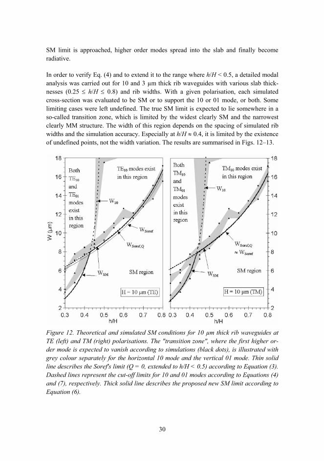
In order to verify Eq. (4) and to extend it to the range where h/H < 0.5, a detailed modal analysis was carried out for 10 and 3 µm thick rib waveguides with various slab thick-nesses (0.25 ≤ h/H ≤ 0.8) and rib widths. With a given polarisation, each simulated cross-section was evaluated to be SM or to support the 10 or 01 mode, or both. Some limiting cases were left undefined. The true SM limit is expected to lie somewhere in a so-called transition zone, which is limited by the widest clearly SM and the narrowest clearly MM structure. The width of this region depends on the spacing of simulated rib widths and the simulation accuracy. Especially at h/H ≈ 0.4, it is limited by the existence of undefined points, not the width variation. The results are summarised in Figs. 1213.
Figure 12. Theoretical and simulated SM conditions for 10 µm thick rib waveguides at TE (left) and TM (right) polarisations. The "transition zone", where the first higher or-der mode is expected to vanish according to simulations (black dots), is illustrated with grey colour separately for the horizontal 10 mode and the vertical 01 mode. Thin solid line describes the Soref's limit (Q = 0, extended to h/H < 0.5) according to Equation (3). Dashed lines represent the cut-off limits for 10 and 01 modes according to Equations (4) and (7), respectively. Thick solid line describes the proposed new SM limit according to Equation (6).
30

Figure 13. Theoretical and simulated SM conditions for 3 µm thick rib waveguides at TE (left) and TM (right) polarisations. For notations refer to Fig. 12.
When h/H > 0.5, there are no TE01 and TM01 modes and the cut-off widths for TE10 and TM10 modes are easily determined. At cut-off, these modes spread into the slab and their local intensity maxima clearly pass the outer edges of the rib. Beyond its cut-off, a propagating mode can usually not be found by the algorithms or the result is clearly a non-physical consequence of the finite calculation area. A calculated waveguide mode is not truly propagating if it is many times wider than the rib, as the power of such a mode will be radiated away by the slightest bend or any other variation along z. The cut-off widths for the TE01 and TM01 modes at h/H < 0.5 are much more difficult to determine unambiguously. Especially when H << 10 µm and h/H << 0.5, the local intensity maxima of these modes do not leave the rib at cut-off. The power ratios between their local intensity maxima change and the modes slowly become leaky, but localised solu-tions can be found even for modes that are clearly too lossy to be considered as propa-gating modes. Close to cut-off, these modes resemble substrate coupled waveguide modes or leaky fiber modes [105: p. 487]. Theoretically these modes settle between propagating and radiating modes. In this work, a mode was considered strictly cut-off if its loss was >10 dB/cm, all the local intensity maxima were not confined below the rib or the intensity distribution was many times wider than the rib. Calculated intensity distri-butions of TE10 and TE01 modes far from cut-off and close to their cut-off limits are shown in Fig. 14.
31

TE10 W = 14 µm
TE01 h/H = 0.3
TE10 W = 9 µm TE01 h/H = 0.45
Figure 14. Calculated intensity distributions of TE10 and TE01 modes far from cut-off (upper row, modes well confined) and close to the cut-off limit (lower row, modes spread into the slab). For TE10 mode rib width W is reduced from 14 to 9 µm (H = 10 µm, h/H = 0.5), while for TE01 mode h/H is increased from 0.3 to 0.45 (H = W = 10 µm). Contour lines represent constant intensity levels with 10% increments.
Rib waveguides with H = 1 and 1.5 µm were also simulated, but the analysis of the re-sults was much more difficult than for H = 10 and 3 µm. All modes were no longer line-arly polarised (no clear TE and TM modes) and the SM limit was very difficult to deter-mine unambiguously. The lack of reliable simulation results in literature also indicates that the modal behaviour of small Si rib waveguides is quite complicated.
Based on the simulations, a new analytical SM condition was proposed and numerically fitted to the results. This new formula is
( )( ) ( )⎪⎩
⎪⎨⎧
>+−+
≤+−+=< −
−
,0HQ4)( if,min
0HQ4)( if2-2
10,
-22,
hQWW
hQWWW
QSoref
QSorefSM
(6)
where
22110)(4)(
1)(−− +−+
++=HQhQ
HQcW , (7)
and c1 is a numerical fitting parameter with an optimum value of -0.1. In addition to the Soref's accurate width limitation (WSoref,Q), another width limitation (W10) is given for eliminating the higher order vertical modes. According to Figs. 1213 the new SM con-dition appears to be at least roughly valid when c1 = −0.1, H = 310 µm and h/H = 0.30.8. It was not yet presented in any of the original publications IVIII. The mathematical
32

form of the proposed formula does not have any clear physical interpretation (yet), but its mathematical characteristics are similar to the analytical expressions presented in Refs. [82, 109]. To gain a deeper understanding of SM condition in rib waveguides, especially in thin and deeply etched rib waveguides, more theoretical considerations and simulation results are required.
In order to give Eq. (6) a more solid basis, a waveguide with H = 3 µm and h/H = 0.3 was analysed also with a 3D BPM algorithm. This method is slower and one needs spe-cial tricks to excite higher order modes near the SM limit. In this work, TE10, TE01, TM10, and TM01 modes were excited one at a time in a clearly MM input waveguide with h/H = 0.15 and W = 1.62.2 µm. The waveguide was then slowly transformed closer to the SM limits by using a method described later in Chapter 2.6. Before final tapering the waveguide had h/H = 0.3 and W = 1.1, 0.8, 0.9, and 0.6 µm for TE10, TE01, TM10, and TM01, respectively. At this point it was checked that all modes were still propagating with negligible losses. Finally, W was slowly decreased until the higher order modes were clearly cut-off and the power originally coupled to them started to radiate into the slab. The estimated SM width limits for the four modes were 1.71.9 µm, 1.21.4 µm, 1.51.7 µm, and 0.81.0 µm, respectively. Corresponding limits according to Eq. (6) are 2.1, 1.1, 1.9, and 0.9 µm, respectively. Thus, the agreement of BPM simulations is rather good with respect Eq. (6). Furthermore, the agreement is excellent with respect to the modal simulation results (compare to Fig. 13).
TE10 W = 2.0 µm TE01 W = 1.5 µm
TE10 W = 1.8 µm TE01 W = 1.3 µm
Figure 15. Cross-sections of 3D-BPM simulations used to check the validity of Eq. (6) for both TE10 (left) and TE01 (right) modes when H = 3 µm and h/H = 0.3. The modes are clearly cut-off between the two shown rib widths and the results agree very well with modal simulations (refer to Figs. 1214).
33

2.3 Optical coupling of fibers and silicon waveguides
Coupling loss in a junction between a SM fiber and a Si rib waveguide is due to four main factors, namely scattering, reflection, modal mismatch and misalignment. Surface roughness in the junction, and especially at the end facet of the Si waveguide, causes scattering losses. Therefore, the waveguide facets must be carefully prepared by polish-ing, cleaving or etching. Reflections appear at all dielectric interfaces, and especially at the Si waveguide's end facet. An air gap between the waveguide and the fiber induces interference due to multiple reflections between the fiber and waveguide ends. However, the gap can be filled with index-matching oil or glue, which effectively leaves a single SiO2-Si interface into the junction. The reflection can then be totally eliminated by add-ing an anti-reflection (AR) coating to the end facet of the waveguide. The optimum n and thickness for a single-layer AR coating between materials 1 and 2 are
21nnnAR = and
( )ARAR nd 4λ= ,
(8)
(9)
respectively. For a SiO2-Si interface nAR ≈ 2.25 and dAR ≈ 172 nm. The optical coupling between a fiber and a Si waveguide is presented schematically (1D) in Fig. 16.
Fiber (n0) Si waveguide (nSi):
Input light Reflected light
Transmitted light
Gap (ngap) AR coating or interface 2
Interface 1
Figure 16. Schematic description of fiber-waveguide input coupling area as a 1D film stack. The gap (n = ngap) is filled e.g. with air, index matching oil or glue. If ngap = n0 = 1.46 then the reflection at the first interface is eliminated. An optional AR coating can be used to eliminate the reflection at the second interface.
In the beginning of this work, waveguides were usually characterised without AR coat-ing and air gap filling, which led to relatively high and unstable reflection losses. The total reflection loss for a single fiber-waveguide junction, as well as for a waveguide chip inserted between input and output fibers, can be estimated analytically by using a 1D film-stack method [VIVII]. This is a valid approximation for large Si waveguides with high optical confinement into the Si core. The reflection coefficients for single SiO2-air, SiO2-Si, and air-Si interfaces are 3.5%, 17%, and 31%, respectively. For an airgap between SiO2 and Si, the theoretical reflection loss is 31±14%. The large variation
34

is due to the interference of multiple reflections. For a long, tilted or absorbing airgap, the loss variation due to multiple reflections is reduced [102]. However, the best way to avoid loss variations is to fill the airgap with index-matching oil or glue, as was done at the later stages of this work. This leads to a constant 17% (0.8 dB) reflection at both ends of the Si waveguide. Taking into account multiple reflections inside the waveguide, the total reflection loss for the SiO2-Si-SiO2 structure is then 25±25% (02.93 dB), with an average of ~1.5 dB. Actual reflection loss in a measurement depends on the waveguide's propagation loss, scattering losses at the dielectric interfaces, and the inter-ference effects. Interference depends on the optical length of the waveguide, as well as on the wavelength and the spectral width of the light source used.
The modal mismatch and the impact of misalignment can be calculated from Eq. (1). In the alignment of SM fibers to Si waveguides there are five degrees of freedom, namely x, y, z, θx, and θy (see Chapter 2.8 for the alignment of PM fibers). When using gaussian mode field approximations for both the fiber and the waveguide, the overall power-coupling efficiency η as a function of radial, longitudinal, and angular misalignments of ∆ρ, ∆z, and θρ, respectively, can be expressed by a formula
( )⎪⎭
⎪⎬⎫
⎪⎩
⎪⎨⎧
⎥⎥
⎦
⎤
⎢⎢
⎣
⎡++
⎟⎟
⎠
⎞
⎜⎜
⎝
⎛+
∆−⋅= 2
22
12
22
22
21
2
211
2exp rr
rr λ
θπρκκη ρ ,
(10)
where
( ) 2222222
21
22
21
/
4
gapnzrr
rr
πλκ
∆++= ,
(11)
r1 and r2 are the 1/e field radii of the gaussian fields, and ngap is the refractive index of the material within the gap [110]. In this thesis, the mode fields of SM and PM fibers were assumed to be gaussian, and to have an 1/e field radius of r1 = rSMF = 5 µm. In case of negligible modal mismatch (r1 = r2 = rSMF), the transverse, longitudinal and rotational alignment accuracies should be below 1 µm, 30 µm, and 1°, respectively, in order to keep the loss <0.2 dB for each axis. The cumulative effect of ∆ρ = 1 µm, ∆z = 30 µm, and θρ = 1° is 0.65 dB. These tolerances are achievable with an appropriate alignment stage, transmitted power as a feedback signal, and a careful alignment procedure. How-ever, fabrication of fixed fiber pigtails is much more difficult. Glues typically experience small deformations during and after curing, and for low-cost applications passive align-ment is usually required.
Numerical overlap calculations were carried out to determine the modal mismatch be-tween the gaussian field of a SM fiber and the modal fields of different Si waveguides more accurately. According to the results, the modal mismatch for Si rib (and strip)
35

waveguides with H = 1014 µm, h/H = 00.6 and an optimised W (1014 µm) varies between 0.1 and 0.5 dB. The optimum coupling is achieved with a 14×14 µm2 strip waveguide (h/H = 0). The requirement for 1 µm transverse alignment accuracy was also numerically confirmed for Si waveguides with H = 1014 µm, h/H = 00.5 and W = 1115 µm. An example of the numerically calculated modal mismatch as a function of the vertical misalignment y is shown in Fig. 17. The optimum width changes very little as a function of misalignment, so the estimated misalignment does not necessarily need to be taken into account in the width optimisation.
0.3
0.35
0.4
0.45
0.50.55
0.6
0.65
0.7
0.75
0 0.25 0.5 0.75 1 1.25 1.5Vertical misalignment y (um)
Cou
plin
g lo
ss (d
B)
W = 11 µmW = 12 µmW = 13 µmW = 14 µm
Loss due to misalignment~0.2 dB wheny = 1 µm
Figure 17. Calculated dependence of modal mismatch between a standard SM fiber and a Si rib waveguide as a function of waveguide width W and vertical misalignment y. Waveguide thickness H = 10 µm and h/H = 0.5.
2.4 Bends and mirrors in Si waveguides
As for the propagating modes of straight waveguides, discrete waveguide modes can also be calculated for waveguides with fixed bending radii. Such waveguides have an invariant cross-section in the cylindrical coordinate system, where the Maxwell's equa-tions can also be applied [111]. In bends, the solutions for the decaying transverse field tails of the mode fields are based on Bessel functions, which are radiative by nature (see e.g. [105: p. 480]). However, the radiation loss for a bend mode may be negligible with a sufficiently large bending radius R, because the radiation losses decrease exponentially as a function of R [103]. For a low-loss and effectively SM bend, the radiation losses should be sufficiently small and high for the fundamental and higher order modes, re-spectively. Higher order bend modes with low losses may be tolerated if power is cou-pled only between the fundamental modes of bends and the SM straight waveguides connected to them. However, this can be quite difficult because of the distorted field profiles of the bend modes. With respect to a straight waveguide with a similar cross-
36

section, the modes of a bent waveguide are shifted away from the centre of curvature, as if they would be affected by a centrifugal force. This induces inter-modal coupling and junction losses at the interfaces between straight and bent waveguides. The overall loss of a fundamental mode due to a bend is, thus, a combination of radiation and junction losses. It can be minimised by optimising the shape of the bend, e.g. by changing R gradually [II].
A significant drawback of a large SM rib waveguide is its sensitivity to bending. Single-moded Si strip waveguides (W×H ≈ 0.13 µm2) may have bending radii around 1 µm [80], while a large Si rib waveguide (e.g. W×H ≈ 100 µm2) may require a 10 mm radius, or more. In this work, the overall bending losses of 1.5, 3 and 10 µm thick rib waveguides were calculated for different radii. The simulations were originally carried out for a Master's thesis [81], supervised by the author. The results are presented in pub-lications III, and summarised below. Some older, and less accurate, bend simulations are also reported in publication III and Chapter 2.5.
Due to the slowness of rigorous bend calculations, the thickness ratio h/H was fixed to 0.5 and the rib widths were chosen according to the Soref's simple SM condition (3). Thus, for H = 1.5, 3 and 10 µm, W = 1.3, 2.6, and 8.8 µm, respectively. Results from the calculations are presented in Fig. 18 as the radiation loss for a 90° bend. The junction losses are excluded from Fig. 18 as they can be minimised by a proper bend design. Radiation loss has a strong polarisation dependency and thinner waveguides have sig-nificantly smaller bending radii with a given tolerable loss (e.g. 0.1 dB/90°). The re-quired bending radius (R >> 10 mm) for a 10 µm thick waveguide with h/H ≈ 0.5 and W ≈ H is not suitable for the dense integration of PICs.
0.01
0.1
1
10
100
0.1 1 10 100
Bending radius R (mm)
Rad
iatio
n lo
ss (d
B/9
0°)
10 µm1.5 µm
3 µmTE
TE TETM
TM
Figure 18. Calculated dependence of radiation losses on waveguide thickness (H = 10, 3, or 1.5 µm), polarisation (TE/TM) and bending radius R.
37

Bending losses can also be reduced by using wider ribs or smaller h/H ratios [93, 111]. This was not studied in the original publications, but some new results are given here. The dependence of bending losses on W and h/H in 10 µm thick waveguides with R = 20 mm was calculated at the end of this work. A new computer (2.8 GHz, 2GB RAM) was used for these simulations, which enabled the densification of the calculation grid by a factor of two in both directions. This improved the simulation accuracy and resulted in somewhat higher losses than those presented above for the same structure. The new results are summarised in Fig. 19. Smaller h/H clearly reduces the bending losses, but at sufficiently small h/H and sufficiently wide rib, higher order modes may also appear with low losses. Based on Fig. 19, a useful compromise for H = 10 µm and R = 20 mm could be e.g. h/H ≈ 0.4, which enables low-loss SM bends when W > 7 µm. Smaller h/H or wider W could enable even smaller R. Unfortunately, accurate calculation of radiation losses for various combinations of H, h/H, W and R values is not practical with available computers and software tools.
0.001
0.01
0.1
1
10
100
0 1 2 3 4 5 6 7 8 9 10 11 12 13 14 15 16W (µm)
Rad
iatio
n lo
ss (d
B/9
0°)
h/H = 0.5
h/H = 0.4
h/H = 0.3
TE
TM
TE
TM
TE
TM
TETM
Higher order vertical modes(TE01, TM01)
Figure 19. Calculated dependence of radiation losses on rib width W, thickness ratio h/H (= 0.5 / 0.4 / 0.3) and polarisation (TE/TM) when H = 10 µm and R = 20 mm. Higher order modes with low-loss can be found if h/H is sufficiently small and W suffi-ciently large.
An alternative for a waveguide bend is a waveguide mirror [112], which uses total inter-nal reflection to deflect the light propagating along one waveguide into another waveguide. In SOI waveguides, the high ∆n enables a deflection angle >90° if the reflec-tion occurs at a Si-SiO2 or Si-air interface (according to Snell's law). Successful reflec-tion requires that the mirror facet be vertical and etched through the whole SOI layer,
38

and that light is well confined into the SOI layer. The mirror can be simply realised into a large multi-moded strip waveguide, as illustrated in Fig. 20. Then the coupling to SM rib waveguides must be separately solved, e.g. with the methods presented in Chapter 2.6. In thin SM strip waveguides significant amount of light bypasses the mirror leading to high losses. Direct integration of a through-etched mirror facet to a rib waveguide requires two masks and accurate alignment between them.
a) b)
Mirror surface
BOX
α/2 α
Si strip waveguide
Fss
Fneottmmhitrm
igure 20. Waveguide mirror in a strip wavegtructure. b) Reflection of light from a waveguoftware recently developed at VTT (top view,
2.5 Directional couplers and
ast and inexpensively mass produced opticaleeded key elements if optical communicationd users. Present switches can be roughly perating above 1 MHz are typically based onion or, in SOI, current injection modulation [8hermal modulation (or moving parts [7]), anore generally, at 0.110 kHz. Switches opore expensive than those operating around 1
ave harmful thermo-optical effects when opes a lack of inexpensive switches and modulatoo have sub-µs response times. Such switcheseconfiguration of optical networks, backup rodulation e.g. in broadband connections to h
39
uide. a) Schematic illustration of a general ide mirror, as simulated with a 2D FDTD W = H = 4 µm, α = 90°).
interferometric switches
switches (and modulators) are one of the n technology is to be brought close to the divided into two speed categories. Those nonlinear effects, electro-optical modula-9]. Slower switches are typically based on d they usually operate around 1 kHz or,
erating above 1 MHz are typically much kHz. Furthermore, the fast switches may rated below 1 MHz [89]. Presently, there rs to operate in the 101000 kHz range or and modulators could be used e.g. in the outing of optical signals, and optical data omes and small offices. [IV]

Si waveguides provide a possibility to realise particularly fast TO switches and modula-tors. Fast modulators have been demonstrated with both SOI waveguides [88, 100] and epitaxially grown Si waveguides [98]. The latter have operated with a 700 kHz band-width, while the SOI modulators have reached up to 40 kHz [88]. However, it should be noticed that these values correspond to a 3 dB modulation depth. For switches the maximum frequency is limited by the required minimum extinction ratio (ER), i.e. the cross-talk between the two (or more) outputs. This should usually be at least 10 dB, which makes fast switches more challenging to fabricate than modulators. A switch can always be used as a modulator, but not vice versa.
In this work, a fast TO switch based on large SOI rib waveguides was designed, fabri-cated, and characterised. Finally, it was accelerated by using a novel modulation tech-nology. The design [III] of the switch started the research of SOI waveguides at VTT by the author in 1997. The SOI technology was chosen because it was rather new, it offered some unique advantages with respect to previous waveguide technologies and it was compatible with the Si processing technology available at VTT. The high thermo-optical constant (1.86⋅10-4 K-1) and good thermal conductivity of Si suggested that there was some potential for realising particularly fast TO switches. Large rib waveguides with good fiber coupling efficiency, and a 2×2 MachZehnder interferometer (MZI) layout with two successive 50:50 directional couplers (DCs) were taken as the design basis. The designed switch layout is schematically illustrated in Fig. 21. As such, the switch is in a cross-state (off), but it shifts into a bar state (on) if a phase difference ∆φ = 180° is intro-duced between the two waveguide branches. This can be induced by operating at least one of the metallic thin film heaters patterned on top of the ribs.
Alternative input waveguide (not used here)
Optical input Output ports:
Bar (ON) Cross (OFF)
Metal film: 4 heaters and 8 contact pads
Waveguide heater Directional coupler
Waveguide S-bend
Figure 21. Schematic top view of the designed 2×2 MZI switch (not in scale).
The switch design involved the analysis, simulation and optimisation for fiber coupling efficiency, S-bends, DCs and thermal modulation. Simulations were carried out with the combination of commercial Optonex software (for 2D optics simulations) and a Matlab toolbox (for 2D thermal simulations). After the switch design, these tools were replaced
40

with more advanced 3D software from BBV Software. Publication III describes the calculation of fiber coupling coefficients and simulation of S-bends, although more accu-rate results are reported in publications III and Chapters 2.32.4. The optimum length for DCs was calculated by using a 2D BPM (top view) and a 2D mode solver (cross-section). The results from the two methods were clearly different, which indicated that 2D BPM and/or the assumption of low ∆n in a mode solver were not applicable for accu-rate SOI rib waveguide simulation.
osses and the required optical insulation between the core and the metallic heater. [IV]
description can be found from publications I and IVV, and from Ref. [66].
the waveguides seriously limits the attainable frequency. The purpose of the new modu-
Thermal simulations indicated that the switch could indeed be somewhat faster than a typical TO switch made of e.g. glass or polymer waveguides. The key to fast heating was the thin oxide cladding that conducts heat rapidly from the heater into the Si rib. On the other hand, fast cooling is possible because the Si slab spreads the heat horizontally and the thin BOX conducts it rapidly into the Si substrate. The speed and power consumption were found to be strongly dependent on the boundary conditions used in the simulation. Airflow around the switch and thermal conductivity through the Si substrate into a sam-ple holder are difficult to estimate accurately. With the used boundary conditions, the heating of one interferometer arm by 3°C required 120 mW of electrical power and changed the switch from cross- to bar-state. The rise (090%) and fall (10010%) times were both 200 µs, corresponding to a maximum frequency of approximately 2.5 kHz. Better heat conductivity away from the rib leads to faster cooling, but it also increases the power consumption. Therefore, BOX thickness and deeply etched insulation grooves [88] can be used to choose a desired speed to power consumption ratio. Smaller waveguides and better heat conductivity into the core can provide a faster switch with lower power consumption, but these approaches are limited by the need for small propa-gation and coupling l
The work described above led to a mask layout (see Figs. 4 and 21) that was used to lithographically pattern all the switches reported in this thesis. It should be noted that the original layout is not thoroughly optimised and that e.g. multi-mode interference (MMI) couplers [23, 113] should be used instead of DCs in future designs. Two heaters were drawn on top of each waveguide branch in order to enable constant power consumption (successive vs. adjacent heaters operated). This also made it possible to modulate the switches with a novel modulation principle, which was invented soon after the mask design. It is briefly summarised below, while a detailed
Traditional modulation is based on turning the heating power P simply on and off in a binary manner (P = Pon or P = 0 W). In some cases bias voltages are used to stabilise the power consumption or to optimise the off-state of a non-ideal switching structure (P = PON or P = Pbias). Traditional modulation can be applied by using simple control electronics, but the exponential stabilisation of the temperature difference ∆T between
41

lation principle is to remove this limit by optimising the time-dependent heating powers P1 and P2 of both waveguide branches during switching operations (rise/fall).
In the new modulation principle, high heating power peaks are used to rapidly heat one waveguide, while the other is cooling down, as illustrated in Fig. 22. Furthermore, at least the off-state is biased, so that both waveguides are equally heated (P1 = P2 = Pbias), and the time-dependence of P1 and P2 during a single switching operation (rise/fall) is optimised, so that ∆φ is stabilised already before the waveguide temperatures T1 and T2 are stabilised. If ∆φ is to be raised from 0 to 180°, P1 forms a high power peak, while P2 drops from Pbias to zero. This increases T1, decreases T2 and rapidly increases ∆φ. Simi-larly, ∆φ can be rapidly decreased from 180 to 0°, by dropping P1 from Pon to zero and by forming a high power peak into P2. For both operations, the fine structures of P1 and P2 are optimised, so that ∆φ reaches and maintains its target range as soon as possible.
The new method is different from the so-called overdriven operation [103: p. 330] be-cause it enables switching with arbitrary input data. It is similar to the method described in [114], but it also enables the reduction of fall-times. Extremely high and sharp heating peaks, and perfectly optimised control signals between them, can provide at least one or two orders of magnitude reduction in response times, while maintaining the obtained phase difference between switching operations. Then heat diffusion into the waveguide core, potential heat accumulation, power consumption, and the availability of control electronics become the fundamental limits for switching speed. However, the new method can be implemented to any desired extent from a minor fine tuning to extreme acceleration by optimising the control signals with the given criteria.
Branch 1 (T1)
P2P1
Branch 2 (T2) Induced temperature difference (arb.units)
Time
Time
Time
OFF rise ON fall OFF
PonPbias0
180°
0°
Heating power
Induced phase difference ∆φ
Figure 22. Schematic illustration of the novel modulation principle.
42

2.6 Multi-step patterning of silicon waveguides
Traditionally, optical waveguides are patterned by using a single mask layer, which is indeed sufficient for many applications. Additional mask layers are often used to define metallic heaters etc, but typically they do not define the waveguide structure. However, with a single mask layer it is difficult to simultaneously define waveguides with SM operation, efficient coupling with fibers, lasers, detectors etc., low-loss propagation, small bending radius, and applicability to miniaturised PICs. Using more than one mask layer in the patterning of a single SOI waveguide cross-section has significant advan-tages, as is explained in detail in publications [III] and Refs. [6365]. Similar approach is already widely used in compound semiconductor devices [115], and it has been ap-plied to SOI waveguides as well [90, 93, 116]. However, those implementations are somewhat different from the ideas described in this thesis, or insufficiently documented for real comparison. In particular, the proposed multi-step patterning principle avoids the complicated epitaxial growth in the middle of waveguide fabrication, and the light is always confined into a single unitary core made of homogeneous Si. The multi-step patterning principle and its potential is illustrated below with four example structures.
The first two waveguide structures transform a rib waveguide into a thin or thick rectan-gular waveguide (or vice versa), as shown in Figs. 23ab. The third transformer waveguide connects two rib waveguides that have different thicknesses, as illustrated in Fig. 23c. The three structures can be combined in various ways, and there is no funda-mental reason to limit the multi-step patterning principle to only two mask layers.
A B C A B C
BOX BOX Si core
a)
b)
c)
Figure 23. Three different 3D waveguide transformers based on multi-step patterning. The layouts on the left describe the structures ac) as seen from the top and the cross-sections A, B, and C are shown on the right.
43

Waveguide transformers, such as those illustrated in Fig. 23, can enable vertical waveguide tapering, coupling between strip and rib waveguides (both with their unique advantages and disadvantages), radical tailoring of both ∆n and the number of propagat-ing modes, and e.g. coupling of light into SM strip waveguides and PhC waveguides. However, the waveguide cross-section must be changed adiabatically, i.e. in a suffi-ciently small angle with respect to the propagation axis. Depending on the type and size of the waveguide, this is expected to require 202000 µm long tapering areas [116]. The mask alignment must also be carried out accurately, although the alignment tolerances can be partially relaxed by using appropriate processing steps [64, 65]. According to simulations, the finite widths and the exact positions of the sharp tips in Figs. 23a and c are not critical, as long as the cross-sectional area is much smaller for the tip than for the underlying rib or strip structure. Thus, an easily attainable tip width of 500 nm is suffi-cient for large structures. The alignment accuracy is around 1 µm in contact lithography and <100 nm in stepper lithography, which are both sufficient for most multi-step struc-tures. It should be noted that outside the transformation area only one mask layer defines the waveguide structure.
The fourth example is a bent rib waveguide with an additional groove etched to its outer side, as illustrated in Fig. 24. The groove locally increases ∆n in the bent waveguide section, and it can almost completely suppress the radiation loss, as can be clearly seen from Fig. 24. In order to minimise the overall bending losses, i.e. both junction and ra-diation losses, the bending radius, as well as the distance and width of the groove, can be adiabatically tuned along the bend. Similar grooves have been proposed for glass waveguides [117, 4: pp. 9799] and briefly referenced for Si waveguides as well [90].
Based on numerous simulations [III], there appears to be significant potential in realis-ing extremely compact PICs based on multi-step SOI waveguides and the advantages should clearly overcome the associated extra efforts in fabrication.
Figure 24. Cross-sections and calculated intensity distributions of bent rib waveguides with R = 20 mm, H = 10 µm, h/H = 0.5, and W = 8.8 µm. a) Without a bend groove (radiation loss 10 dB/90°). b) With a bend groove (radiation loss 0.0002 dB/90°). Con-tour lines with 10% spacing between 5 and 95%.
44

2.7 Waveguide gratings
Fiber optic gratings are widely used for reflecting desired wavelength(s) backwards along a fiber or, in general, for producing a desired reflection spectrum. Fiber gratings are usually fabricated by using ultraviolet (UV) light to produce small refractive index changes along a piece of fiber. Waveguide gratings on planar substrates [VI, VII, 62, 90, 91] represent a less mature technology, but they have some clear advantages, especially with respect to fabricating miniaturised gratings and in integrating several different grat-ings and other optical functions on a single chip.
In this work, waveguide gratings were designed for SOI waveguide technology in col-laboration with the Department of Physics at the University of Joensuu (JoFy). The work is reported in publications VIVII and in Ref. [62]. The target application was an add-drop filter which could be fabricated by adding identical corrugated gratings on top of the two waveguide branches of a 2×2 MZI, as illustrated in Fig. 25a. In order to have efficient fiber coupling and SM operation, the gratings were to be etched on top of ~10 µm thick rib waveguides with h/H ≈ 0.5 and W = 710 µm. Therefore, light is expected to be well confined into the Si core with the neff of the fundamental mode being slightly below 3.5. This means that for a first order grating the period should be λ/(2neff) ≈ 220 nm and the width of the corrugation groove ~110 nm. Such small structures are extremely diffi-cult to fabricate with good surface quality, although they can result in compact devices.
a)
λ1, λ2, λ3, λ4,... (in)
λ2 (drop) λ1, λ2', λ3, λ4,... (out)
λ2' (add) Reflection peak at λ2
b)
Figure 25. Schematic illustration of a) an add-drop filter and b) the designed waveguide grating.
First, the effective index change ∆neff as a function of H, W and groove depth was calcu-lated for grooves only on top of the rib and grooves extending to the surrounding slab (see Fig. 25b). The latter produced much higher ∆neff values, although even they were <0.0002 if the grating depth was <500 nm, and W ≈ H = 710 µm. The estimated maxi-mum achievable etch depth for the grating was 500 nm. The required grating length as a function of ∆neff was then calculated with a 1D film stack method. In order to have rela-
45

tively short gratings with >99% reflection, the grating should be as deep as possible and it should preferably extend to the slab region as well.
The results were confirmed with a rigorous 2D simulation tool that was specially devel-oped for this task. The new simulation method is based on rigorous diffraction theory. It is much more accurate than the film stack method, computationally efficient and appli-cable to the analysis of other corrugated gratings as well. The 2D approximation was implemented by eliminating the horizontal coordinate, thus describing the surface corru-gation accurately. However, the approximation presents a SM rib waveguide as a highly MM slab waveguide. This led to the identification of additional reflection peaks that correspond to non-physical higher order modes that in reality present loss. Based on the results, deeper etching enables shorter gratings, but at etch depths >>1 µm coupling to higher order vertical modes leads to harmful losses. The effect of stitching errors in e-beam lithography was also studied. [VI]
2.8 Polarisation cross-talk
Theoretically, propagating waveguide modes have no polarisation cross-talk. In practice, however, waveguides have a finite polarisation cross-talk due to junctions, process non-idealities, and non-adiabatic transformations. In most applications the input polarisation is unknown and it is sufficient to optimise the components with respect to polarisation dependent loss (PDL) and polarisation mode dispersion (PMD). However, in some po-larisation maintaining applications the cross-talk between different polarisation modes should be minimised. This typically requires waveguides with sufficiently high birefrin-gencies, low losses, and accurately aligned input junctions. It is possible to realise PM components with low PDL and PMD, but usually components are designed to be either highly polarisation independent (with SM fiber pigtails) or polarisation maintaining (with PM fiber pigtails). In the following, the theory of polarisation cross-talk in Si waveguide components is briefly discussed. More details and experimental results are given in Chapter 3.3, publications [I, VIII] and Ref. [63].
In literature, the term polarisation extinction ratio is commonly used to describe the characteristics of polarisers, PM fibers, waveguides, light propagating in free space and light originating from the end of a fiber or a waveguide [VIII]. In this thesis, the PXR of light that propagates along a SM fiber, or originates from the end of that fiber (PXRout), is defined as the ratio of optical powers P1 and P2 coupled to the two differently polar-ised fundamental modes of the fiber, i.e. PXR = 10⋅log10(P1/P2) dB. This and the follow-ing definitions apply for waveguides as well as for fibers. Usually, the two fundamental modes are linearly polarised along two mutually orthogonal polarisation axes. In PM fibers these axes are called the slow and the fast axis, while in Si waveguides the axes are horizontal (TE) and vertical (TM) with respect to the chip. Linear polarisation modes are assumed in this thesis, which is a good approximation for PM fibers and large Si rib
46

waveguides. Then PXRout can be measured as the ratio of powers transmitted through a linear polariser aligned along the two polarisation axes. This PXR value depends on input coupling (PXRin), polarisation cross-talk in the fiber and the order of the modes (P1/P2 or P2/P1). The PXR of the fiber itself is defined as its PXRout (>1) when PXRin = 0 or ∞. In practise, accurate characterisation of devices requires that PXRin >> PXRout and that the rotational misalignments at the input and output are kept well below arctan(1/PXRout).
In general, PXR(α) is the ratio of powers P1 and P2 transmitted through a linear polariser in two orthogonal angles α (P1) and α+90° (P2). It describes the PXRin that would couple to a fiber rotationally aligned to angle α. If α is the angle with respect to a fiber's polari-sation axis,
1)cos()tan(PXR2)(tanPXR
)(tan)cos()tan(PXR2PXR)(PXR
out2
out
2outout
+∆−
+∆+=
φαα
αφαα ,
(12)
where PXRout and ∆φ are the PXR and the phase difference of the polarisation modes at the fiber's output. This formula was used to analyse the changing of PXR due to rota-tionally misaligned junctions, and to explain the measured PXR(α) curves. It is illus-trated in Fig. 26 and it led to the invention of a novel method for measuring the polarisa-tion axes of waveguides and polarisation maintaining fibers. According to the proposed method, two or more PXR(α) curves are measured and their crossing point determines the angle of a polarisation axis (α = 0°). In this method, ∆φ does not need to be known or densely varied. It suffices to change it enough for the identification of the crossing point(s), e.g. by ±45°, or more. Changes can be induced by heating, bending or stretch-ing the fiber (or waveguide), or by slightly changing the wavelength. If some interpola-tion or fitting to theoretical curves is used, the measurement accuracy can be much better than the angular step size. Also, the measurement accuracy of this method can be esti-mated based on curve fitting and/or deviation of crossing points between multiple PXR(α) curves.
It should be noted that if ∆φ is properly averaged out, e.g. by using a sufficiently broad-band light source, then PXR(α) corresponds to ∆φ = 90°. For light propagating in free space, there are no modes or polarisation axes, and PXR is usually defined as the maxi-mum of a measured PXR(α) curve. Sometimes this definition is also used to determine PXRout of a fiber or a waveguide. However, based on Eq. (12) and Fig. 26 this should be used only if ∆φ is averaged out. Otherwise the maximum PXR(α) indicates a false angle and a false PXRout.
47

Figure 26. Theoretical PXR curves based on Eq. (12). PXRin = 20 dB and ∆φ = 0°, 45°, 90°, 135°, or 180°.
As can be concluded from Eq. (12) and Fig. 26, the rotational misalignment of a fiber with respect to the input of a Si waveguide rapidly increases the variation of the waveguide's input PXR with respect to ∆φ, which is usually unknown and unstable. Therefore, the rotational alignment should be carried out very accurately, especially in case of multiple successive junctions between different PM components.
Proper input alignment alone does not guarantee high PXRout for a Si waveguide. The polarisation cross-talk within the waveguide or the waveguide component must also be minimised. Careful PIC design can minimise unwanted modal coupling in bends, tapers and other circuit elements. However, material inhomogeneities, surface roughness around the core and other process-related imperfections induce scattering losses, and some of the scattered power tends to couple to the other polarisation. This type of cross-talk can be minimised by decreasing the propagation losses and by increasing the waveguide birefringence.
48

3. Fabrication 3.1 Clean-room processing
The fabrication of waveguide components was mostly based on standard clean-room processes and tools that are commonly used in silicon microfabrication. An up-to-date introduction to microfabrication can be found from [105]. The basic principle of photo-lithographic patterning is illustrated in Fig. 27. A short summary of the used tools and methods is given in this chapter. Due to the numerous variations of processing, a default process for fabricating an SOI waveguide chip is first described and the main variations with respect to that are then briefly listed.
UV light Photomask Photosensitive resist Oxide hard mask Silicon
Oxide hard mask Silicon
c)
Silicon
d) Etching plasma (anisotropic, material selective) Silicon
Etching plasma (anisotropic, mrial selective)
ate-a)
b)
Figure 27. Schematic presentation of photolithographic surface patterning with an oxide hard mask (dimensions not in scale). a) UV exposure. b) Resist development. c) Oxide dry etching. d) Si dry etching.
The default waveguide process is based on photolithographic patterning and the use of an oxide hard mask (see Fig. 27). First, approx. 300 nm thick oxide hard mask is depos-ited with low temperature oxide (LTO) process in a chemical vapour deposition (CVD) furnace on top of a BESOI wafer with SOI thickness ~10 µm. Waveguide patterns are then transferred to the hard mask using standard photolithography and dry oxide etching in parallel plate plasma etcher. Silicon etching is done using an inductively coupled plasma (ICP) type reactive ion etcher (RIE). The etching process is modified from a pulsed (Bosch) type process for deep silicon etching, in which etching and passivation steps are alternated subsequently. The etching and passivation gases are SF6 and C4H8, respectively. During the passivation step a thin polymer film is deposited on the etched silicon side-walls to prevent lateral etching under the mask and thus keeping the etched wall vertical. The passivation and etching step lengths are reduced to their minimum (5 s) to minimise the depth of the unavoidable side-wall undulation in this process. The process is started by etching the first 500 nm with continuous passivation to prevent the significant underetching in a first etch cycle when no passivation is yet present. The resulting etch wall roughness after Si etching is shown in Figs. 28ab. After the removal of the resist and the passivation polymers in oxygen plasma, the oxide mask is removed
49

by wet etching in hydrofluoric acid. The final process step is the deposition of the top cladding oxide. By default, the cladding is formed by thermal oxidation, which also reduces surface roughness on waveguide walls. The default TOX thickness is 1 µm.
b) a)
Fca(w
TminmvpomAet
Intup(dtotostptietFstsu
igure 28. Scanning electron microscope (SEM) imted with the default process, but before claddinghite area is the BOX layer). b) Side wall (undulati
o eliminate the slight undulation in waveguide waay alternatively be used. In this case, the flow rcreased linearly as a function of time, instead of paximum achievable etch depth is presently limited
erticality. There are alternatives to the TOX top ressure CVD of oxides, such as tetraethyl orthosilir the cladding deposition can be simply skipped. Fetal heaters must be processed on top of the rib wal layer was sputter deposited and patterned usingching.
order to enable the future demonstration of funres, a three-step fabrication process was also deve
resented in Fig. 29. First the default waveguide proeepest areas in the final structure). Then a new m define the layout for the third etch step. This stru Si, but a new photoresist layer is applied and patep is done using the photoresist mask. Then the posed oxide hard mask is used to carry out the thirons of the three mask layouts (etch steps 13) canch 1, 3, 1+3, 2+3, or 1+2+3). Examples of fabrig. 30. When applied to functional waveguides on ructures should provide adiabatic operation as lofficiently small crossing angles with respect to eac
50
ages of SOI rib waveguides fabri- oxide deposition. a) Cross-section on due to the pulsed process).
lls, a continuous passivation process ate of the passivating gas (C4F8) is ulsed operation. In this process, the to ~6 µm with acceptable side wall cladding as well. For example, low cate (TEOS) and LTO, can be used, or fabricating TO switches, thin film veguides. By default, a 500 nm thick standard photolithography and dry
ctional multi-step waveguide struc-loped. The process is schematically cess is applied for the first etch step ask oxide is deposited and patterned cture is not immediately transferred terned on top of it. The second etch hotoresist is stripped off and the ex-d etch step. The different combina- produce six final Si levels (no etch, icated test structures are shown in SOI wafers (see Chapter 2.6), these ng as the different mask lines have h other.

Oxide mask Resist
f) Oxide mask
Silicon
Silicon
Silicon
Oxide mask
Silicon
Oxide mask
g)
h)
Silicon
Oxide mask Resist
i)
a)
Silicon
b) Oxide mask
Silicon
c) Oxide mask
Silicon
d)
Oxide clad-ding
e) Silicon
Figure 29. Schematic presentation of a multi-step process (3 etch steps, dimensions not in scale). a) Oxide patterning with photomask 1. b) Silicon etching with oxide mask and oxide removal. c) Oxide deposition. d) Oxide patterning with photomask 3. e) Resist patterning with photomask 2. f) Si etching with resist mask. g) Resist removal. h) Silicon etching with oxide mask. i) Final structure after oxide removal and thermal oxidation.
No etch Etch 1 Etch 2+3
Etch 3
5 µm 2 µm
Figure 30. SEM images of fabricated multi-step test structures on Si wafers. The differ-ent combinations of etch steps are indicated on the right.
51

3.2 Post-processing and fiber pigtailing
Between the clean-room processing and sample characterisation, some post-processing is usually required. In this work, the main post-processing steps were wafer dicing (into chips), polishing of the chip facets to optical quality and wire bonding of electronic con-tacts to TO switches. Dicing was carried out with a Loadpoint MicroAce 3 machine. An improved dicing method was developed for optical samples in order to ease the polishing process.
In the beginning of this work, chip polishing was carried out by using diamond sprays and rapidly rotating polishing cloths. This process was slow and it only provided moder-ate surface quality. Therefore, better polishing equipment was purchased and a new polishing process was developed for SOI waveguide samples. With the latest process, fine tuned by another person at VTT, a chip facet with an array of SOI waveguides can be polished to excellent quality in less than half an hour. One key factor in a successful polishing process is that the chip surface is protected with a thick resist layer until the final chip cleaning. In order to characterise the TO switches the contact pads on the chips were wire-bonded to external electronics.
In this work, single-layer AR coating technology was developed to reduce reflections in fiber-waveguide junctions. Three coating materials were tested, namely Ta2O5 (n = 2.1), HfO2 (n = 2.03), and ZrO2 (n = 2.13). All three materials were grown by atomic layer deposition (ALD), but the first two were deposited at the University of Helsinki, while ZrO2 was deposited at the Helsinki University of Technology. Lowest reflections were measured with an AR coating made of Ta2O5. However, the variation of measured re-flection coefficients between different materials and samples was dominated by thick-ness variation, not the refractive index differences. The thicknesses were not thoroughly calibrated in this work. Nevertheless, it should be noted that in series production the ALD thickness uniformity is usually excellent and all the three materials are applicable for AR coatings. Another, and perhaps even more important, advantage of ALD is excel-lent conformality (step-coverage).
Some waveguide samples were equipped with fixed fiber pigtails, and even with fiber arrays. First, fibers were passively aligned onto Si V-groove chips and fixed with UV-curable glue and glass lids. Then these fiber sub-assemblies were polished and actively aligned to the waveguide chips. Finally, the aligned end facets were fixed together with UV-curable and index-matched glue.
52

3.3 Waveguide gratings and photonic crystal structures
The experimental part of the waveguide grating development was started in the very beginning of the whole research work, in parallel with the study of thermo-optical switching. Therefore, this work did not only concentrate on the waveguide gratings themselves, but it also involved a significant amount of fundamental development with respect to the processing of plain silicon waveguides and various types of silicon nanos-tructures with the help of both optical and electron (e)-beam lithography [VII, 62, 70].
As was explained in chapter 0, the target for process development was to realise up to 500 nm deep corrugated gratings on top of an SOI rib waveguide and the nearby slab regions (refer to Fig. 25b). The design for process integration involved the patterning of wide gratings onto an SOI wafer, the patterning of an oxide hard mask on top of the grating and, finally, the etching of silicon around the rib to the desired depth, so that the grating around the rib would be replicated on top of the slab. The fabrication processes for rib waveguides and gratings were first develop separately, while bearing in mind the requirement for process integration in the future. The developed waveguide process was similar to the above described default process and its detailed description can be found from publication VII. The grating process was first intended to be carried out mostly at JoFy in Joensuu, but it was found out that such a process formed a contamination risk to the CMOS fabrication line at VTT. Most of the fabrication steps were then moved to VTT's facilities in Espoo and only the critical e-beam lithography step was done at JoFy. Numerous processing tests were done with different mask layers and etch processes, but first order gratings with 225 nm period could not be fabricated with sufficient quality because of an artefact in e-beam writing. The varying e-beam dose resulted in linewidth and, consequently, etch depth variations (see Fig. 31a). However, second and third order gratings (450 and 675 nm periods) with over 1 µm etch depth were successfully realised on plain Si wafers (see Fig. 31b).
After developing the waveguide and grating processes separately, they were combined with the designed integration process. First and third order grating structures were fabri-cated on top of silicon ribs on both Si and SOI wafers (see Fig. 31c). Unfortunately, the gratings around the ribs had poor quality. Apparently, the replication of the surface cor-rugation from the original Si surface to the lower slab surface by using anisotropic sili-con dry etching around the rib was not successful. Residual hard mask oxide in the grat-ing grooves at the beginning of the deep Si etching was at least one of the reasons for this. The high quality of third order gratings was maintained on top of the ribs, but the gratings on the sides did not have sufficient quality for successful optical measurements. However, the obtained ability to realise over 1 µm deep gratings opened up the possibil-ity to apply gratings only on top of the ribs in future experiments.
53

450 nm 225 nm a) b)
c)
2.7 µm = 4×675 nm
Figwideµm
ThphsucFigturtra
Fige-b
ure 31. SEM images of fabricated gratith period 225 nm and depth ~1 µm. b) Aspth. b) Parallel grating on top of a Si rib (fabricated only for SEM analysis).
e success of fabricating nanostructures otonic crystal components on 1 µm thiccessfully [70, 84]. Some PhC waveguide . 32. To enable the optical characterisatie, input and output coupling of light shoted in Fig. 23a may turn out to be useful f
ure 32. SEM images of PhC waveguide seam exposure window: a) 60° bend, b) 12
5
ng test structures. a) Grating on a Si wafer
above, but with 450 nm period and 1.2 µmstructure with period 675 nm and depth 1.2
on flat surfaces enabled the fabrication of k SOI wafers. This was indeed carried out structures fabricated in SOI are illustrated in on of these tiny PhC waveguides in the fu-uld still be developed. The structure illus-
or this purpose.
tructures fabricated in SOI by using a single 0° bend, and c) taper.
4

4. Experimental results 4.1 Construction of the measurement set-ups
In the beginning of this work, measurements were carried out with an unstable 6-axis alignment stage, standard SM and MM fibers (SMF, MMF), rotatable thin-film polaris-ers, standard objectives and an IR camera. This resulted in many problems, including difficult fiber alignment and unexplained polarisation effects. Therefore, a rigid 3-axis alignment stage with piezo drives (NanoBlock from Melles Griot), a computer controlled 6-axis stage (Model F-206 from PI), PM fibers (PMF, from Flextronics), a fiber pigtailed polariser (from General Photonics), two free-space polarisers (PXR 50 dB, from Thor-labs), a PM fiber coupler (from Newport), two PM 1×2 switches (from Newport), two polarisation splitters (from OZ optics), and a new IR camera with near-field optics were purchased. Furthermore, a motorised fiber rotator was fabricated by a student from The Finnish School of Watchmaking under author's supervision. With these tools, new setups for loss and polarisation measurements were constructed. The basic setups are illustrated in Figs. 3334 (alignment tools not shown), although some modifications were made for particular measurement needs.
Laser
Switch TE PMF
Pol. splitter PMF
TE / TM Fiber rotatation 90°
DUT TE→TM
PMF Polariser
PMF a)
Laser PMF TE / TM DUT
Rotatable polariser PMF b)
DUT EDFA
SMF (16 dBm output power from amplifier noise)
(Unpolarised light) c)
SMF (Unpolarised light)
Halogen lamp
Objective
DUT d)
PMF
Pol. splitter DUT PMF
45° angle Broadband LED source e)
Figure 33. Typical measurement setups used for optical input coupling. ab) TE/TM polarised input for insertion loss (IL), PDL, PXR, and polarisation axis measurements. c) High power input for IL measurements. d) Input for spectral measurements. e) Polar-ised broadband input for birefringence measurements. EDFA = erbium doped fiber amplifier, DUT = device under test.
55

a)
Rotatable polariser
DUT
Objective
Det. MMF Spectrum
analyser DUT d)
MMF DUT
Spectrum analyser
Objective Det. DUT
e) b)
IR camera 2
Near field optics IR camera 1 DUT
For coarse alignment
DUT Det. SMF or MMF c)
f)
Figure 34. Typical measurement setups used for optical output coupling in measurement of a) polarised output power and PXR, b) output power in free-space, c) output power with SMF or MMF, d) PXR spectra for birefringence measurements, e) spectral charac-teristics and f) near-field intensity distributions. Det. = detector.
Compared to the old setups and methods, the new setups provided significantly better measurement accuracy. This also led to much better consistency with the theory and simulations. High quality polishing of the waveguide facets (see Chapter 3.2) and the use of index matching oil between fibers and waveguides were also found to be crucial for obtaining reliable results.
4.2 Optical coupling of fibers and silicon waveguides
Silicon rib waveguides were optically coupled with standard SM, MM and PM fibers. The coupling efficiency to MM fibers is practically 100%, excluding the reflection losses. Modal mismatch between a Si rib waveguide and a standard SM fiber was deter-mined by measuring the insertion losses (IL) of 3 mm long waveguide chips between SM input and output fibers. Due to the short waveguide length the propagation losses are negligible (<0.1 dB) with respect to the coupling losses, and the worst-case coupling loss estimate for a single fiber-waveguide junction is IL/2, including the reflection losses. The reflection losses were suppressed to 0.8±0.05 dB/facet by using index matching oil (n = 1.5) between the fiber and the waveguide. To estimate the modal mismatch loss, 0.75 dB/facet reflection loss was subtracted from IL/2 (interference effects should be very small with the used light source). For 9 µm thick test waveguides with h/H ≈ 0.48 the measured minimum modal mismatch loss was 0.6 dB with W ≈ 12 µm (width varia-tion in 1 µm steps). According to rigorous overlap calculations for the same H and h, minimum losses of 0.541 and 0.584 dB for TE and TM, respectively, should be obtained at W ≈ 13 µm. Thus, the calculated and measured values agree very well.
56

The impact of AR coatings in reducing the reflection losses was measured with 4 cm long waveguide chips. In order to eliminate the somewhat uncertain propagation losses (0.20.8 dB), insertion losses for the waveguides were measured before and after AR coating deposition. Index matching oil was used for both measurements, and the IL re-duction after AR coating was compared to the calculated loss reduction. The best results were obtained with Ta2O5 AR coatings and they are summarised in Table 1. The average loss reduction was 0.8 dB/facet with a 0.12 dB standard deviation (due to the finite measurement accuracy). The calculated loss reduction was 0.7 dB for a 180 nm thick Ta2O5 coating. This thickness was measured from a reference sample, and it may slightly deviate from the real thickness. Thus, the calculated and measured values again agreed very well. Based on the results and the calculated 0.8±0.05 dB reflection loss without the AR coating, the reflection loss with the AR coating is estimated to be <0.15 dB. Thus the total coupling loss for a 9 µm thick waveguide with AR coating and optimum alignment is estimated to be <0.75 dB/facet. Even lower coupling loss should be attainable with an optimised AR coating thickness and a thicker waveguide. With an optimal Ta2O5 coating and a 14×14 µm strip waveguide, the coupling loss could be as low as 0.1 dB/facet.
Table 1. Insertion losses (dB) of Si rib waveguides between standard SM fibers with and without Ta2O5 AR coatings, and the insertion loss reduction (dB) due to the AR coating. LWC = line width change with respect to the nominal W on the mask layout.
H h/H LWC Nominal W: (µm) (µm) 14 µm 13 µm 12 µm 11 µm 10 µm
Without Ta2O5 9.1 0.35 -2 3.0 3.2 3.2 3.3 3.8 With Ta2O5 1.8 1.4 1.9 1.8 2.0
IL reduction 1.2 1.8 1.3 1.5 1.8 Without Ta2O5 8.5 0.38 -2.3 3.2 3.1 3.4 3.7 3.8
With Ta2O5 1.9 1.7 1.6 1.8 2.3 IL reduction 1.3 1.4 1.8 1.9 1.5
Coupling with PM fibers was also tested. To obtain good input PXR the polarisation axes of the waveguides and fibers were accurately aligned parallel. The polarisation axes of a Si waveguide are usually parallel and transverse to the chip's surface and, thus, easy to align with respect to the setup. However, the polarisation axes at plain fiber ends need to be directly measured. After the measurement the fiber axes can be rotated parallel to the waveguide axes and the positional alignment can be started. In this work, two alter-native methods were used to find the polarisation axes of PM fibers. In the first method, broadband light source was used to average out the phase differences between the polari-sation modes. Thus, the maximum and minimum of PXR(α), as measured by a rotatable polariser, indicated the angles of the polarisation axes. Due to its simplicity and suffi-cient accuracy, this method was usually used. However, the practical applicability of the new measurement method, as introduced in Chapter 2.8, was also demonstrated [VIII].
57

The new measurement method was tested by using three alternative means to induce phase difference changes in a PM fiber. All three led to good results, but heating pro-vided slightly better accuracy than wavelength tuning and mechanical fiber manipula-tion. The improved accuracy was mostly due to the motorised fiber rotator, which was used only in the heating experiments. It was not yet available when the other modulation methods were tested. Fitting to theoretical curves was good for temperature and wave-length tuning, but rather poor for the mechanical fiber manipulation. This was due to the uncontrolled and unexpectedly long stabilisation time of microscopic fiber movements, which induced phase fluctuations during the angular scan. With temperature modulation the measured PXR(α) curves fitted well to theory and provided a measurement accuracy of better than 0.2°, as can be confirmed from Fig. 35.
When compared to alternative methods [118121], the new method has some unique advantages. Unlike the broadband method, the new method can be applied also to de-vices with a very narrow spectral range, such as arrayed waveguide gratings (AWGs) or wavelength filters. Compared to the use of polarisation analysers, or other complicated equipment, the new method is particularly simple and inexpensive to implement. Some alternative methods are based on measuring PXR(α) continuously with a fast rotating polariser. However, with these method one needs to vary both α and ∆φ with very small steps. The accuracy of the new method appears to be at least as good as for any other method, and it can be easily confirmed from the results.
Figure 35. Measurement of a PM fiber's polarisation axis by heating the fiber (filled symbols) and by using a broadband light source (thin crosses).
Finally, fixed fiber pigtails were fabricated by using a combination of passive fiber alignment into Si V-groove chips and active alignment between the fiber array and waveguide array chips (see Fig. 5a). This was done for both SM and PM fibers. For PM fibers the output PXR of the fiber array was limited to ~17 dB, even if the fiber align-ment was done with very high accuracy. This was probably due to the stress induced into
58

the PM fibers when they were permanently affixed to the V-grooves with UV-curing glue and a pyrex lid. For SM fiber arrays the fixed fiber pigtails increased the coupling losses by <0.5 dB/facet with respect to the optimum alignment of single fibers. Thus, the misalignments in a fiber array were <1.5 µm according to Fig. 17.
4.3 Propagation and bending losses of silicon waveguides
Accurate measurement of the propagation losses in low-loss Si rib waveguides is quite difficult. In this work, 4" SOI wafers were used, providing a maximum length of 9 cm for straight waveguides. For 9 cm long waveguides with 0.10.5 dB/cm attenuation the total propagation loss is comparable to the somewhat uncertain coupling losses. Also, low-loss light propagation in the surrounding slab makes it difficult to separate the pow-ers associated with the fundamental, higher order and radiation modes at the output of short waveguide samples. Thus, the usual cut-back method [77, 79] does not provide very accurate results for low-loss waveguides. On the other hand, the very high effective index requires that short waveguides should be used in the alternative FabryPerot loss measurement [77, 79]. Then the scattering losses at the waveguide end facets induce uncertainties in the loss measurements.
In order to measure the propagation losses accurately, up to 114 cm long spiral wave-guides were fabricated on 100 mm SOI wafers. A schematic layout of the spiral is shown in Fig. 36. Nominal waveguide width varied from 2 to 11 µm, and the bending radius varied between 25 and 42 mm along the spiral. The minimum radius of 25 mm is still quite short for weakly guided Si rib waveguides with H ≈ 9 µm and h/H ≈ 0.5, and the bending losses have some effect on the measured propagation losses. Also, each waveguide made 100 crossings with other waveguides. Thus, the measured losses are a worst-case estimate. However, the impact of fiber coupling and interference effects is almost completely eliminated in the very long waveguides, and the insertion loss of perpendicular crossings is very small (<0.05 dB/crossing based on the results). Reflec-tion loss with index matching oil is only 0.8 dB/facet, while even the smallest measured IL was ~15 dB. To obtain the propagation loss, 0 and 1.6 dB losses were assumed for crossings and reflections, respectively. Also, the calculated modal mismatch loss was subtracted from the IL.
Most of the results were obtained with a high-power EDFA source (Fig. 33c) and SM or MM fibers at the output (Fig. 34c). Some polarisation measurements were carried out with a laser source and PM fibers (Figs. 33a and 34a). The waveguides were confirmed to be SM by monitoring the output with an IR camera while moving the input fiber. Straight waveguides with same dimensions were often seen to be multi-moded because the bends eliminate weakly guided higher order modes. In practise, wider waveguides can, and should, be used in bends.
59

Five adjacent waveguide arrays forming a spiral
Maximum bending radius 42 mm
Input waveguide array (individual waveguides not shown here)
Minimum bending radius 25 mm
Crossings Output waveguide array (W = 2−11 µm)
Wafer edge (radius 50 mm)
Figure 36. Schematic layout of the waveguide spiral test structure used to determine the propagation losses of Si rib waveguides.
The measured minimum propagation loss for 114 cm long and 9 µm thick SM rib wave-guides between two SM fibers was 0.13±0.01 dB/cm. This waveguide was fabricated with the continuous passivation process. It had h/H ≈ 0.44, W ≈ 7 µm, and a calculated modal mismatch of 1.2 dB/facet. According to Eq. (6), the maximum SM width is 7.4 and 7.2 µm for TE and TM, respectively. Thus, the waveguide was SM also according to Eq. (6). The obtained propagation loss is the best reported so far in literature for a dry etched Si rib waveguide at λ ≈ 1550 nm. Also, the measurement accuracy is much better than in previous results at λ = 13001550 nm. For example, in [72] the propagation loss at λ = 1.52 µm is reported to be 0±0.5 and 0.4±0.5 dB/cm for TE and TM, respectively.
Propagation losses were also measured as a function of wavelength for 9.0, 4.9, and 2.0 µm thick SM waveguides. For a 9.0 µm thick spiral waveguide the propagation loss was practically constant (0.13−0.16 dB/cm) from 1200 to 1650 nm. For H ≈ 4.9 µm and H ≈ 2.0 µm the minimum propagation loss measured from a 71 mm long straight waveguide was 0.3±0.2 dB/cm and 1.2±0.2 dB/cm, respectively. To obtain these values the calculated modal mismatch and reflection losses were subtracted from the measured insertion losses. This reduced the measurement accuracy of thin and straight waveguides compared to the thick spiral waveguides. However, it can be clearly seen that thinner waveguides have higher propagation losses due to their higher sensitivity to surface roughness. The measured transmission spectra are shown in Fig. 37.
0
0.5
1
1.5
2
2.5
1150 1200 1250 1300 1350 1400 1450 1500 1550 1600 1650
Wavelength (nm)
Prop
agat
ion
loss
(dB
/cm
)
H = 9.0 µm, W = 6.7 µm
H = 4.9 µm, W = 4.4 µm
H = 2.0 µm, W = 3.6 µm
Figure 37. Measured propagation loss spectra for single-moded 9.0, 4.9, and 2.0 µm thick Si rib waveguides.
60

4.4 Polarisation characteristics of Si waveguides and directional couplers
The birefringencies of different Si rib waveguides were measured by using the fixed analyser method [122]. The used input and output setups are illustrated in Figs. 33e and 34d, respectively. The results are also described in publication [I] and Ref. [63]. In the measurements both polarisation modes of the waveguide were equally excited (PXRin ≈ 0 dB) from an input PM fiber having high PXR and a rotational 45° angle with respect to the waveguide. At the output, a PXR spectrum was measured, again at 45° angle with respect to the waveguide. Waveguide birefringence induces a periodic variation of measured PXR as a function of λ, and the birefringence can, thus, be concluded from the measured λ-period and sample length. Examples of measured PXR spectra and birefrin-gence values as a function of rib width W are shown in Fig. 38. Measurements were carried out for 9 µm thick rib waveguides with different widths and cladding materials (h/H ≈ 0.5). The main conclusion was that typical cladding oxide materials (n ≈ 1.5), such as TOX and LTO, can increase the birefringence almost by an order of magnitude compared to an air cladding. This must be due to the stress induced by the cladding into the Si core [I, 63, 95]. A low-stress TEOS cladding indeed provided almost as low bire-fringence as the air cladding, although both values were at the limits of measurement accuracy. A summary of the results is given in Table 2. [I]
-30
-20
-10
0
10
20
30
1350 1400 1450 1500 1550 1600
Wavelength (nm)
PXR
(dB
)
LTO
TEOS
0
1
2
3
4
5
6
7
8
2 4 6 8 10
Waveguide width (µm)
Bire
fring
ence
(10-4
)
Figure 38. a) Measured PXR spectra from two 4 cm long waveguides with LTO and TEOS claddings (H ≈ 9 µm, h/H ≈ 0.5, W ≈ 8 µm). b) Measured birefringence as a func-tion of W in a 71 mm long sample chip with TOX cladding (H ≈ 9 µm, h/H ≈ 0.5).
Waveguide width can also be used to tune the birefringence, but this may produce con-flicts with other design criteria, such as low-loss and SM operation. However, by choos-ing an appropriate cladding material and by fine tuning cladding thickness, waveguide width and etch depth, one should be able to tune the birefringence continuously from
61
very small values (polarisation independent operation) to very high values (PM opera-tion). Some variations can also be done within a single chip to monolithically combine waveguides with different polarisation characteristics. Finally, it should be noted that in thin waveguides birefringence usually increases [93, 95] and becomes a more difficult problem.
Table 2. Calculated and measured birefringencies of rib waveguides with different clad-ding materials, all with H ≈ 9 µm, h/H ≈ 0.5 and W ≈ 8 µm. Calculated values do not include stress-induced birefringence, unlike the measured values.
Calculated: Measured:
Cladding material: Air SiO2 Air TEOS LTO TOX
Birefringence (10-4): 0.236 0.238 <1 1 6 6.3
For realising polarisation independent devices it is not always sufficient to minimise birefringence only. After all, birefringence-induced PMD is usually not very significant in the relatively short waveguide chips. Instead, the polarisation dependency of all opti-cal circuit elements, such as directional couplers and modulators, must be minimised, although there is usually a strong correlation between birefringence and the polarisation dependency of components. In this work, the polarisation dependency of directional couplers was tested for different cladding materials, namely air, TEOS, LTO and TOX. According to the results, there was indeed a strong correlation with birefringence. Air and TEOS claddings provided polarisation independent DC operation, while LTO and TOX caused a strong polarisation dependency. Therefore, LTO and TOX should not be used for polarisation independent applications.
Birefringence measurements indicate that LTO and TOX claddings could be used for PM applications, particularly if only one polarisation is used. However, such applica-tions require a sufficient PXR value for waveguides and waveguide components, such as DCs. Therefore, the PXR of straight Si waveguides and DCs was measured. The PXR of the input fiber was >30 dB and the polarisation angles were accurately aligned with the methods described in Chapter 2.3. Furthermore, the input angle was iteratively varied in order to confirm optimum alignment. Output PXR was measured with both the broad-band method and the new crossing point method. However, the maximum output PXR of both straight waveguides and DCs was only slightly over 15 dB. This value is rather low, although sufficient for some applications. It is estimated that the relatively low PXR is due to scattering, which is also responsible for propagation losses. A certain fraction of the scattered light is coupled to the opposite polarisation state, and the PXR can only be improved by further reducing the propagation losses. This conclusion is supported by the fact that in a 4 cm long waveguide with 0.15 dB/cm loss 13% of the input power is scat-tered away from the waveguide, while PXR = 15 dB corresponds to 3.6% of the same input power having coupled to another polarisation state.
62

4.5 Fast thermo-optic 2x2 MZI switch
First thermo-optic 2×2 MZI switches were fabricated directly after the switch and mask design (see publication III and Chapter 2.5). However, the initial characterisation of the switches [28] was not easy, because the pre-existing measurement setup was somewhat unstable, the input polarisation was arbitrary, and the quality of the waveguide facets was rather poor. Also, the unprotected Mo thin film heaters experienced corrosion and the heating of the waveguide chip influenced the fiber coupling efficiency at the input due to the thermal expansion or warping of the chip. The measurement setup and the facet polishing process were then improved, as explained in Chapters 4.1 and 3.2, re-spectively, and heatsinks were attached to the waveguide chips. This stabilised the power and polarisation at the input. Furthermore, waveguide processing was developed further to reduce scattering losses, and ~200 nm thick Mo heaters were replaced with 500 nm thick Al heaters. The final dimensions of waveguides were H ≈ 9 µm, h ≈ 5 µm, and W ≈ 9 µm. Waveguide spacing was 250 µm at the input, output and heating area, and 11 or 12 µm in the directional couplers. A bending radius of 12 cm was used for the S-bends to induce transverse offsets of ~120 nm, and the lengths of the DCs were varied between 0 and 4 mm. This led to a total chip length of 4 cm. For more details on switch process-ing, see publications I and IVV, and Chapter 3.1. After the development described above, new switches were fabricated and characterised. As the DCs were polarisation dependent (see Chapter 4.4), only TE polarisation was used for the characterisation (setup as in Figs. 33a and 34c). Details of switch modulation can be found from publica-tions I and IVV.
First, the MZI switches were characterised without heating. The best switches had an output extinction ratio ER = |10log(TCROSS/TBAR)| ≈ 17 dB (98:2), where TCROSS and TBAR are the relative powers from the two switch output ports (BAR and CROSS with respect to the input port). This was partly due to the very coarse variation of DC lengths on the mask. For example, only lengths 0, 1, 1.5, 2, and 3 mm were available for 11 µm waveguide separation. Therefore, the measured maximum ER does not indicate the maximum for SOI-based MZI switches in general.
Heating contacts were wire bonded to the best switches, which were then characterised with externally applied control signals. First, the voltage over a single heater was slowly increased in order to determine the minimum and maximum transmissions for both out-put ports. The minimum and maximum were obtained with heating powers P = 0 W and P = PON = 300 mW, respectively. Same 17 dB extinction ratio was found for the ON and OFF state (∆φ = 0 or π). However, the ER of a lossless and symmetric MZI should be infinite for the ON state [III]. Therefore, the ER is not limited only by the DC lengths, but also by scattering, inter-modal coupling, limited PXR or some other imperfection. If we assume that a fixed fraction s of total output power is always divided equally to both outputs, e.g. due to scattering, then the relative CROSS port transmission (or portion of total output power if the switch has an excess loss) is
63

[ ]( ) ssrT211cos(1
2sin
21 2
CROSS +−∆+⎟⎠⎞
⎜⎝⎛= φπ ,
(13)
where r is the ratio of real and ideal DC length. Relative transmission to the BAR port is TBAR = 1−TCROSS. The maximum and minimum transmissions TCROSS,max and TCROSS,min are obtained at ∆φ = 0 (OFF) and π (ON), respectively. By measuring them one can simply determine the remaining switch parameters
min,CROSS2Ts = and
min,CROSS
min,CROSSmax,CROSS2212
sinT
TTr−
−=⎟
⎠⎞
⎜⎝⎛ π .
(14)
(15)
Equal ER exima (±17 dB) indicate that TCROSS,max ≈ 1−TCROSS,min , DC length is close to optimum (r ≈ 1) and s ≈ 0.04 dominates the maximum ER. The relatively high s is probably due to scattering, and it could be lowered by reducing the excess loss of the switch, which was measured to be ~1 dB with respect to an equally long straight waveguide. It should be noted that the maximum output ER of ±17 dB describes perfect phase control, and that in the following results the emphasis is in the phase modulation depth. For any measured TCROSS with an arbitrary ∆φ, one can calculate the ideal trans-mission TCROSS,ideal corresponding to an ideal MZI structure (r = 1, s = 0) from
min,CROSSmaxCROSS,
min,CROSSCROSSlCROSS,idea TT
TTT
−
−= .
(16)
This value, or the corresponding ideal extinction ratio
dB1
log10ERlCROSS,idea
lCROSS,ideaideal ⎟
⎟⎠
⎞⎜⎜⎝
⎛
−=
TT
, (17)
should be used to evaluate the depth of the thermo-optic phase modulation.
After the preliminary characterisation the best switches were characterised with fast externally applied control signals. First, simple step-wise modulation (ON/OFF) was applied to one heater only. The maximum modulation frequency for 15 dB ER (ERideal = 20 dB) was 10 kHz. The measured CROSS-port transmission at 10 kHz operation is shown in Fig. 39. The measured speed and power consumption of the switch were somewhat higher than in simulations. The heat conductivity from the Si substrate to the heat sink was probably higher than in simulations.
64

The feasibility of the novel modulation method (see Chapter 2.5) was tested by using it to accelerate the TO switch. At first, a simple, inexpensive, and somewhat slow control electronics was built with a minimum time-step of 1 µs. This defined a maximum fre-quency of 167 kHz for the new modulation method. The rise and fall operations were then shortened by optimising the heating powers P1 and P2 of the two waveguide branches in 1 µs time-steps. The switching state could then be changed in 3 µs with 15 dB ER. This could be done either once or with a continuous 167 kHz frequency. With better electronics, higher frequencies could have been obtained with lower ER.
00.10.20.30.4
Hea
ting
pow
er(W
)
00.250.5
0.751
0 50 100 150 200 250Time (µs)
Nor
mal
ized
tra
nsm
issi
on
Figure 39. Measured CROSS-port transmission (lower graph) of the TO Si waveguide switch with traditional 10 kHz modulation (upper graph). Transmission is normalised to the attainable range of the slightly non-ideal switch (199%).
Sensitivity to random modulation was tested by sending semi-random bit sequences as inputs to the control electronics. This dropped the measured ER to 13 dB (ERideal = 15 dB). Optical response to a semi-random input signal at 167 kHz is shown in Fig. 40. With a random input signal the average power consumption was 150 mW for the traditional 10 kHz modulation and 590 mW for the novel 167 kHz modulation, i.e. the speed and the power consumption increased by factors 17 and 3.9, respectively. Thus, the acceleration was efficient with respect to the increase in heating power.
In order to reach even faster operation, new control electronics was constructed and used to optimise single switch transitions with 9 dB ER (1090%) [V]. Single rise and fall times were successfully suppressed to 725 and 700 ns, respectively. For comparison, a traditional modulation method provided 29 and 35 µs transition times, i.e. 4050 times slower operation. If the single transitions are carried out with an average frequency of 1 or 10 kHz, the power consumption increases 4 and 44%, respectively, when compared to traditional modulation with the same OFF-state bias power. Thus, the acceleration was again efficient with respect to the increase in heating power.
65

00.5
11.5
22.5
Hea
ting
pow
er 2
(W
)
0
0.25
0.5
0.75
1
0
Nor
mal
ised
trans
mis
sion
00.5
11.5
22.5
Hea
ting
pow
er 1
(W)
0 1 1 0 0 1 0 1 0 0 0 1
Figure 40. SemirP1 and P2 (middleattainable range
Based on the resufor H ≈ 10 µm) isuch as silica or of Si and the thiappropriate BOXspeed and power operation and lowfeasibility of theimprovement byswitches operatinobtained 167 kHreported so far inobtained with higcies would be muthe new modulatsuch as slower sil
3 6 9 12 15 18 21 24 27 30 33 36Time (µs)
andom input data at 167 kHz frequency (top), optimised heating powers ), and the measured TCROSS (bottom). Transmission is normalised to the (199%) of the slightly non-ideal TO Si waveguide switch.
lts, TO switching appears to be approximately tenfold faster (~10 kHz n Si waveguides than in equally large low index contrast waveguides, polymer waveguides [18]. This is due to the good thermal conductivity n BOX and cladding layers. Thermal insulation grooves [88] and an layer thickness can be used to obtain a desired compromise between consumption. Furthermore, smaller waveguides can provide both faster er consumption at the cost of more complicated fiber coupling. The
new modulation method was successfully demonstrated with a speed a factor of 1750 with respect to traditional modulation. For TO g at λ ≈ 1550 nm and having good mode matching with SM fibers, the z frequency and sub-µs switching times are clearly the fastest results literature. In particular, one should keep in mind that these results are h ER values of 1320 dB. For 3 dB modulation, the maximum frequen-ch higher than those reported above. The promising results indicate that ion principle should be tested also with other interferometric devices, ica and polymer switches, and 1×1 MZI modulators.
66

5. Conclusions In this work, theoretical, numerical and experimental studies were carried out in order to promote Si waveguide technology. Based on the theoretical and numerical studies, a new SM condition and the use of multi-step patterning for Si waveguides were proposed. Novel methods were also invented for accelerating interferometric devices and for measuring the polarisation axes of waveguides and PM fibers. A small contribution was also given for the development of a new simulation method for corrugated waveguide gratings.
Numerous waveguides and waveguide components were fabricated by using standard and modified clean-room processes. Existing processes were improved, especially for realising low-loss Si rib waveguides. New processes were developed for multi-step pat-terning, as well as for patterning ~1 µm deep corrugated gratings and photonic crystal waveguides with a combination of e-beam lithography and two types of dry etching. Post-processing steps were also developed, especially waveguide facet polishing, anti-reflection coating, and fiber pigtailing.
For the characterisation of fabricated devices, new setups and methods were developed. Propagation losses as low as 0.13±0.01 dB/cm were accurately measured for 9 µm thick Si rib waveguides by using a 114 cm long spiral waveguide. This is the lowest propaga-tion loss reported so far for SM dry etched Si waveguides at λ ≈ 1550 nm. Modal mis-match between SM fibers and 9 µm thick Si rib waveguides was measured to be 0.6 dB, while thicker Si waveguides are expected to have mismatch losses as small as ~0.1 dB. The reflection losses at Si waveguide end facets were suppressed from 0.71.6 dB/facet to <0.15 dB/facet by using a Ta2O5 AR coating. Losses due to misalignments in fixed fiber pigtail arrays were kept below 0.5 dB/facet with 1.5 µm alignment accuracy. This included the impact of passive alignment into V-grooves and active alignment between fiber and waveguide arrays. Waveguides were pigtailed also with PM fibers. This in-volved the accurate rotational alignment between fibers and waveguides. For this pur-pose, also the invented new rotational alignment method was tested, and its accuracy was found to be better than 0.2°. At least for some applications, the new method appears to be more simple and accurate than the alternative methods. Waveguide birefringence was found to vary between 0.0001 and 0.00063 depending on the cladding material. This enables the fabrication of both polarisation independent and maintaining Si waveguides. However, the polarisation extinction ratio of waveguides and directional couplers was found to be only ~15 dB. This should be improved by further reducing the propagation losses.
Finally, the fabricated thermo-optical switches with non-optimised directional couplers were modulated with a traditional step-wise method and the invented novel modulation method. The former provided a maximum frequency of 10 kHz with 15 dB extinction
67
ratio and an average power consumption of 150 mW. The new method provided a maximum frequency of 167 kHz with the same ER and an average power consumption of 590 mW. Therefore, the frequency and the power consumption were increased by factors 17 and 3.9, respectively. It should be noted, that the measured 15 dB ER corre-sponds to a 20 dB ER in an ideal switch structure. With improved control electronics and a slightly lower ER of 9 dB, single rise and fall times were suppressed down to 725 and 700 ns, respectively. The continuous 167 kHz modulation frequency and the single tran-sition times of ~0.7 µs represent the fastest values reported so far for thermo-optic waveguide switches operating at λ ≈ 1550 nm and having efficient fiber coupling (thick-ness >5 µm).
Considering all the possibilities for extreme photonic circuit miniaturisation and mono-lithic integration with e.g. electrical and micromechanical functions, silicon micro-photonics is a fascinating research area with a lot of potential for scientific and commer-cial success. However, silicon microphotonics, and Si waveguide technology in particu-lar, are also a very challenging subject. Some of the main difficulties are the high capital cost of fabrication tools, sensitivity to surface roughness, polarisation dependence, diffi-culties in vertical tapering, and the requirement for 1 µm alignment accuracy in hybrid assembly. Also, the present lack of sufficient computer power for accurate 3D simula-tions in macroscopic scale complicates the design and theoretical analysis of Si waveguide devices. Furthermore, the indirect bandgap and negligible electro-optic con-stant of Si have so far prevented the realisation of optical light sources and fast modula-tors that would be competitive with other photonic technologies, such as compound semiconductors and lithium niobate. These drawbacks have prevented at least the silicon waveguides from making a true commercial success, although low index contrast waveguides on Si have already become widely used in optical communication.
The advantages of Si waveguides are estimated to appear especially in the mass produc-tion of photonic devices with high quality and sufficient complexity, as well as in the future integration between various optical, electronic and mechanical functions on a single chip. In the present optical communication market the demand for such devices is quite low. However, it is estimated that the further development of silicon microphoton-ics and the revival of the market can change the situation both radically and rapidly. During the past few years this technology has already evolved with huge steps. At the same time, numerous companies, universities and research organisations have started to study Si waveguide technology, which shows that there is a common belief in it.
Hopefully, this thesis will contribute to the future success of silicon microphotonics. In a wider perspective, the potential success of silicon microphotonics can provide a new technological development step for the whole Silicon Age.
68

References 1. http://www.intel.com/technology/itj/2002/volume06issue02/art02_processdev/
vol6iss2_art02.pdf
2. http://www.intel.com/technology/itj/2004/volume08issue02/art05_on-chip/ p02_intro.htm
3. G. E. Moore, "Cramming more components onto integrated circuits", Electronics 38, pp. 114117, 1965.
4. L. Pavesi, D.J. Lockwood (Eds.), Silicon Photonics, Topics in Applied Physics, 94, Springer, 2004. 397 p. ISBN 3-540-21022-9.
5. International Technology Roadmap for Semiconductors: 2003 Edition (ITRS 2003), http://public.itrs.net
6. M. Paniccia, M. Morse, and M. Salib, "Integrated photonics", in [4], pp. 5188, 2004.
7. M. Hoffmann and E. Voges, "Bulk silicon micromachining for MEMS in optical communication systems", J. Micromech. Microeng. 12, pp. 349360, 2002.
8. J. Kiihamäki, J. Dekker, P. Pekko, H. Kattelus, T. Sillanpää, and T. Mattila, "Plug-up a new concept for fabricating SOI MEMS devices, Microsystems Technologies 10, pp. 346350, 2004.
9. S. Roy, R. G. DeAnna, C. A. Zorman, and M. M. Mehregany, "Fabrication and characterization of polycrystalline SiC resonators", IEEE Electron Device Lett. 49, pp. 43234332, 2002.
10. A. Torkkeli, Droplet microfluidics on a planar surface, PhD Thesis, VTT Publications 504, Espoo, Finland, 194 p. + app. 19 p., 2003. ISBN 951-38-6237-2; 951-38-6238-0. http://www.vtt.fi/inf/pdf/publications/2003/P504.pdf
11. M. Ylimaula, M. Åberg, J. Kiihamäki, and H. Ronkainen, "Monolithic capacitive pressure sensor with CMOS readout circuit", Proc. 29th European Solid-State Circuits Conf. (ESSCIRC 2003), pp. 611614, 2003.
12. N. Maluf, An introduction to microelectromechanical systems engineering, Artech House, 2000. 265 p. ISBN 0-89006-581-0.
13. Z. Gaburro, "Optical interconnect", in [4], pp. 121176, 2004.
14. J. Wieland, H. Duran, and A. Felder, "Two-channel 5 Gbit/s silicon bipolar monolithic receiver for parallel optical interconnects", Electron. Lett. 30, pp. 359359, 1994.
69

15. P. Friis, K. Hoppe, O. Leistiko, K. B. Mogensen, J. Hübner, and J. P. Kutter, "Monolithic integration of microfluidic channels and optical waveguides in silica on silicon", Appl. Opt. 40, pp. 62466251, 2001.
16. S. Franssila, Introduction to microfabrication, John Wiley & Sons, 2004. 401 p. ISBN 0-470-85105-8.
17. J. D. Plummer, M. D. Deal, and P. B. Griffin, Silicon VLSI Technology: Funda-mentals, Practice, and Modeling, Prentice Hall, 2000, 817 p. ISBN: 0130850373.
18. E. J. Murphy (Ed.), Integrated optical circuits and components, Marcel Dekker, Inc, 1999, 449 p. ISBN: 0-8247-7577-5.
19. A. Splett, J. Schmidtchen, B. Schüppert, and K. Petermann, "Low loss optical ridge waveguides in a strained GeSi epitaxial layer grown on silicon", Electron. Lett. 26, pp. 10351037, 1990.
20. G. Cocorullo, F. G. Della Corte, M. Iodice, I. Rendina, and P. M. Sarro, "Silicon-on-insulator rib waveguides with a high-confining ion-implanted lower cladding", IEEE J. Sel. Top. Quantum Electron. 4, pp. 983989 1998.
21. G. Bonfrate, M. Harlow, C. Ford, G. Maxwell, and P. D. Townsend, "Asymmet-ric MachZehnder germanosilicate channel waveguide interferometers for quan-tum cryptography systems", Electron. Lett. 37, pp. 846867, 2001.
22. S. Janz, "Silicon-based waveguide technology for wavelength dicision multiplex-ing ", in [4], pp. 323360, 2004.
23. P. Katila, T. Aalto, P. Heimala, and M. Leppihalme, "Optical waveguides for 1064 nm and chip pigtailing with PM fibers", Proc. 4th Int. Conf. on Space Op-tics (ICSO 2000), Toulouse, France, 57 December 2000, pp. 635640, 2000.
24. G. D. Maxwell and B. J. Ainslie, "Demonstration of a directly written directional coupler using UV-induced photosensitivity in a planar silica waveguide", Elec-tron. Lett. 31, pp. 9596, 1995.
25. K. Wörhoff, P. V. Lambeck, and A. Driessen, "Design, tolerance analysis, and fabrication of silicon oxynitride based planar optical waveguides for communica-tion devices", J. Lightwave Technol. 17, pp. 14011407, 1999.
26. P. Heimala, P. Katila, J. Aarnio, and A. Heinämäki, "Thermally tunable inte-grated optical ring resonator with poly-si thermistor", J. Lightwave Technol. 14, pp. 22602267, 1996.
70

27. K. K. Lee, D. R. Lim, A. Agarwal, K. Wada, and L. C. Kimerling, "Scattering losses in a high ∆n waveguide system for silicon microphotonics", Mat. Res. Soc. Symp. Proc. 637, paper E3.4, 2001.
28. M. Leppihalme, T. Aalto, P. Katila, P. Heimala, M. Blomberg, and S. Tammela, "Si-based integrated optical and photonic microstructures", Proc. SPIE 3936, pp. 215, 2000.
29. M. A. Green, J. Zhao, A. Wang, P. J. Reece, and M. Gal, "Efficient silicon light-emitting diodes", Nature 412, pp. 805808, 2001.
30. L. Pavesi, L. Dal Negro, C. Mazzoleni, G. Franzò, and F. Priolo, "Optical gain in silicon nanocrystals", Nature 408, pp. 440444, 2000.
31. L. Khriachtchev and M. Räsänen, "Optical gain in Si/SiO2 lattice: Experimental evidence with nanosecond pulses", Appl. Phys. Lett. 79, pp. 12491251, 2001.
32. ST Microelectronics (http://www.stmicroelectronics.com), Press release 29 Octo-ber 2002.
33. S. Coffa, G. Franzò, and F. Priolo, "High efficiency and fast modulation of Er-doped light emitting Si diodes", Appl. Phys. Lett. 69, pp. 20772072, 1996.
34. Y. C. Yan, A. J. Faber, and H. de Waal, "Erbium-doped phosphate glass waveguide on silicon with 4.1 dB/cm gain at 1.535 µm", Appl. Phys. Lett. 71, pp. 29222924, 1997.
35. H.-S. Han, S.-Y. Seo, and J. H. Shin, "Coefficient determination related to optical gain in erbium-doped silicon-rich oxide waveguide amplifier", Appl. Phys. Lett. 81, pp. 37203722, 2002.
36. F. Iacona, D. Pacifici, A. Irrera, M. Miritello, G. Franzò, F. Priolo, D. Sanfilippo, G. D. Stefano, and P. G. Fallica, "Electroluminescence at 1.54 µm in Er-doped Si nanocluster-based devices", Appl. Phys. Lett. 81, pp. 32423244, 2002.
37. L. Diehl, S. Menteşe, E. Müller, D. Grützmacher, H. Sigg, U. Gennser, I. Sagnes, Y. Campidelli, O. Kermarrec, and D. Bensahel, "Electroluminescence from strain-compensated Si0.2Ge0.8/Si quantum-cascade structures based on bound-to-continuum transition", Appl. Phys. Lett. 81, pp. 47004702, 2002.
38. R. Claps, D. Dimitropoulos, and B. Jalali, "Stimulated Raman scattering in silicon waveguides", Electron. Lett. 38, pp. 13521354, 2002.
39. R. Claps, D. Dimitropoulos, Y. Han, and B. Jalali, "Observation of Raman emis-sion in silicon waveguides at 1.54 µm", Optics Exp. 10, pp. 13051313, 2002.
71

40. B. Jalali, R. Claps, D. Dimitropoulos, and V. Raghunathan, "Light generation, amplification and wavelength conversion via stimulated Raman scattering in sili-con microstructures", in [4], pp. 199238, 2004.
41. R. J. Curry, W. P. Gillin, A. P. Knighs, and R. Gwillam, "Silicon-based organic light-emitting diode operating at a wavelength of 1.5 µm" Appl. Phys. Lett. 77, pp. 22712273, 2000.
42. D. L. Mathine, H. S. Woo, W. He, T. W. Kim, B. Kippelen, and N. Peyghambar-ian, "Heterogeneously integrated organic light-emitting diodes with complemen-tary metal-oxide-silicon circuitry", Appl. Phys. Lett. 76, pp. 38493851, 2000.
43. L. Dal Negro, M. Cazzanelli, N. Daldosso, Z. Gaburro, L. Pavesi, F. Priolo, D. Pacifici, G. Franzo, and F. Iacona, "Stimulated emission in plasma-enhanced chemical vapour deposited silicon nanocrystals", Physica E 16, pp. 297308, 2003.
44. L. Pavesi, "Will silicon be the photonic material of the third millenium?", J. Phys. Condens. Matter 15, pp. 11691196, 2003.
45. R. Claps, V. Raghunathan, D. Dimitropoulos, and B. Jalali, "Anti-stokes Raman conversion in silicon waveguides", Optics Exp. 11, pp. 28622872, 2003.
46. S. Kimura, K. Maio, T. Doi, T. Shimano, and T. Maeda, "Photodetectors mono-lithically integrated on SOI substrate for optical pickup using blue or near-infrared semiconductor laser", IEEE Trans. Electron Dev. 49, pp. 9971004, 2002.
47. D. M. Kuchta and H. A. Ainspan, "Performance of fiber optic data links using 670 nm CW VCSEL's and a monolithic Si photodetector and CMOS preampli-fier", IBM J. Res. & Development. 39, pp. 6372, 1995.
48. H. Zimmermann, K. Kieschnick, M. Heise, and H. Pless, "BiCMOS OEIC for optical storage systems", Electron. Lett. 34, pp. 18751876, 1998.
49. Schaub, J. D., Li, R., Csutak, S. M. and Campbell, J. C., "High-speed monolithic photoreceivers on high resistivity and SOI substrates", IEEE J. Lightwave Tech-nol. 19, pp. 272278, 2001.
50. H. Zimmermann, "Silicon photo-receivers", in [4], pp. 239268, 2004.
51. J. Ho and K. S. Wong, "High-speed and high-sensitivity silicon-on-insulator metal-semiconductor-metal photodetector with trench structure", Appl. Phys. Lett. 69, pp. 1618, 1996.
72

52. S. Fama, L. Colace, G. Masini, G. Assanto, and H.-C. Luan, "High performance germanium-on-silicon detectors for optical communications", Appl. Phys. Lett. 81, pp. 586588, 2002.
53. G. Masini, L. Colace, G. Assanto, H.-C. Luan, and L. C. Kimerling, "High-performance p-i-n Ge on Si photodetectors for the near-infrared: From model to demonstration", IEEE Trans. Electron Dev. 48, pp. 10921096, 2001.
54. L. Colace, G. Masini, G. Assanto, H.-C. Luan, K. Wada, and L. C. Kimerling, "Efficient high-speed near-infrared Ge photodetectors integrated on Si sub-strates", Appl. Phys. Lett. 76, pp. 12311233, 2000.
55. H. Lafontaine, N. L. Rowell, S. Janz, and D.-X. Xu, "Growth of undulating Si0.5Ge0.5 layers for photodetectors at λ=1.55 µm", J. Appl. Phys. 86, pp. 12871291, 1999.
56. F. Y. Huang, X. Zhu, M. O. Tanner, and K. L. Wang, "Normal-incidence strained-layer superlattice Ge0.5Si0.5/Si photodiodes near 1.3 µm", Appl. Phys. Lett. 67, pp. 566568, 1995.
57. A. Splett, T. Zinke, K. Petermann, E. Kasper, H. Kibbel, H.-J. Herzog, and H. Presting, "Integration of waveguides and photodetectors in SiGe for 1.3 µm op-eration", IEEE Photon. Technol. Lett. 6, pp. 5961, 1994.
58. S. Winnerl, D. Buca, S. Lenk, Ch. Buchal, S. Mantl, and D.-X. Xu, "MBE grown Si/SiGe undulating layer superlattices for infrared light detection", Mat. Sci. Eng. B 89, pp. 7376, 2002.
59. M. El kurdi, P. Boucaud, S. Sauvage, G. Fishman, O. Kermarrec, Y. Campidelli, D. Bensahel, G. Saint-Girons, I. Sagnes, and G. Patriarche, "Silicon-on-insulator waveguide detector with Ge/Si self-assembled islands", J. Appl. Phys. 92, pp. 18581861, 2002.
60. M. El kurdi, P. Boucaud, S. Sauvage, O. Kermarrec, Y. Campidelli, D. Bensahel, G. Saint-Girons, and I. Sagnes, "Near-infrared photodetector with Ge/Si self-assembled quantum dots" , Appl. Phys. Lett. 80, pp. 509511, 2002.
61. P. G. Kik, A. Polman, S. Libertino, and S. Coffa, "Design and performance of an erbium-doped silicon waveguide detector operating at 1.5 µm", J. Lightwave Technol. 20, pp. 862867, 2002.
62. T. Aalto, S. Yliniemi, P. Heimala, P. Pekko, J. Simonen, and M. Kuittinen, "Inte-grated Bragg gratings in silicon-on-insulator waveguides ", Proc. SPIE 4640, pp. 117124, 2002.
73
63. T. Aalto, P. Heimala, S. Yliniemi, M. Kapulainen, and M. Leppihalme, "Fabrica-tion and characterization of waveguide structures on SOI", Proc. SPIE 4944, pp. 183194, 2003.
64. T. Aalto / Valtion Teknillinen Tutkimuskeskus, "Optical waveguide for integrated optical circuit and method for producing the optical waveguide", PCT Patent Ap-plication WO 03/085429 A1, Priority date 11 April 2002, Publication date 16 Oc-tober 2003.
65. T. Aalto / Valtion Teknillinen Tutkimuskeskus, "Optical waveguide ", PCT Pat-ent Application WO 03/085430 A1, Priority date 11 April 2002, Publication date 16 October 2003.
66. T. Aalto, M. Kapulainen, M. Harjanne, and M. Rönö / Valtion Teknillinen Tut-kimuskeskus, "Method for controlling an optoelectronic component", PCT Patent Application WO 2004/023196 A1, Priority date 4 September 2002, Publication date 18 March 2004.
67. T. Aalto / Valtion Teknillinen Tutkimuskeskus, "Method and device for deter-mining the rotational angle of the polarisation axis of an optical waveguide or fi-ber", PCT Patent Application WO 2004/065921 A1, Priority date 24 January 2003, Publication date 5 August 2004.
68. T. Aalto / Valtion Teknillinen Tutkimuskeskus, PCT Application PCT/FI2004/000299, Priority date 18 May 2004, to be published 18 November 2005.
69. B. Jalali, S. Yegnanarayana, T. Yoon, T. Yoshimoto, I. Rendina, and F. Cop-pinger, "Advances in silicon-on-insulator optoelectronics", IEEE J. Sel. Top. Quantum Electron. 4, pp. 938947, 1998.
70. S. Yliniemi, T. Aalto, P. Heimala, P. Pekko, K. Jefimovs, J. Simonen, and T. Uusitupa, "Fabrication of photonic crystal waveguide elements on SOI", Proc. SPIE 4944, pp. 2331, 2003.
71. B. Jalali, "Silicon-on-insulator photonic integrated circuit (SOI-PIC) technology", Proc. SPIE 2997, pp. 6071, 1997.
72. A. G. Rickman, G. T. Reed, "Silicon-on-insulator optical rib waveguides: loss, mode characteristics, bends and Y-junctions", IEE Proc.-Optoelectron. 141, pp. 391393, 1994.
73. W. P. Maszara, R. Dockerty, C. F. H. Gondran, P. K. Vasudev, "SOI materials for mainstream CMOS technology", Electrochem. Soc. Proc., Ed. S. Christoloveanu, 97, pp. 1526, 1997.
74. SOITEC, manufacturer of Smart-Cut SOI wafers, http://www.soitec.com
74

75. Canon, commercial manufacturer of ELTRAN SOI wafers, http://www.canon.com/technology/detail/device/soi/index.html
76. E. D. Palik, Handbook of optical Constants of Solids, Academic Press Inc., 1985.
77. W. Bogaerts, Nanophotonic waveguides and photonic crystals in silicon-on-insulator, PhD Thesis, Universiteit Gent, 2004. 271 p.
78. A. Sakai, T. Fukazawa, T. Baba, "Low loss ultra-small branches in a silicon pho-tonic wire waveguide", IEICE Trans. Electron. E85-C, pp.10331038, 2002.
79. K. K. Lee, D. R. Lim, and L. C. Kimerling, "Fabrication of ultralow-loss Si/SiO2 waveguides by roughness reduction", Opt. Lett. 26, pp. 18881890, 2001.
80. Y. A. Vlasov and S. J. McNab, "Losses in single-mode silicon-on-insulator strip waveguides and bends", Optics Exp. 12, pp. 16221631, 2004.
81. M. Harjanne, Design of tight bends in optical waveguides, Master's Thesis, Hel-sinki University of Technology, 2003. 58 p. In Finnish.
82. R. A. Soref, J. Schmidtchen, K. Petermann, "Large single-mode rib waveguides in GeSi-Si and Si-on-SiO2", IEEE J. Quantum Electron. 27, pp. 19711974, 1991.
83. K. Hosomi, T. Katsuyama, "A dispersion compensator using coupled defects in a photonic crystal", IEEE J. Quantum Electron. 38, pp. 825829, 2002.
84. S. Yliniemi, J. Simonen, T. Aalto, P. Heimala, "Fabrication of silicon nanostruc-tures for photonic crystal applications", Proc. 4th Int. Conf. on Materials for Mik-roelectronics and Nanoengineering, Espoo, Finland, 1012 June 2002. IOM Communications Ltd, 2002. ISBN 1-86125-155-6.
85. T. W. Ang, G. T. Reed, A. Vonsovici, A. G. R. Evans, P. R. Routley, M. R. Josey, "0.15 dB/cm loss in Unibond SOI waveguides", Electron. Lett. 35, pp. 977978, 1999.
86. Fischer U., Zinke T., Kropp J.-R., Arndt F., Petermann K., "0.1 dB/cm waveguide losses in single-mode SOI rib waveguides", IEEE Photonics Technol. Lett. 8, pp. 647648, 1996.
87. T. Zinke, U. Fischer, B. Schüppert, K. Peterman, "Theoretical and experimental investigation of optical couplers in SOI", Proc. SPIE 3007, pp. 3039, 1997.
88. S. A. Clark, B. Culshaw, E. J. C. Dawnay, and I. E. Day, "Thermo-optic phase modulators in SIMOX material", Proc. SPIE 3936, pp. 1624, 2000.
75

89. P. Dainesi, A. Küng, M. Chabloz, A. Lagos, Ph. Flückiger, A. Ionescu, P. Fazan, M. Declerq, Ph. Renaud, Ph. Robert, "CMOS compatible fully integrated MachZehnder interferometer in SOI technology", IEEE Photon. Technol. Lett. 12, pp. 660662, 2000.
90. T. Bestwick, "ASOCTM A silicon-based integrated optical manufacturing tech-nology", Proc.48th IEEE Electronic Components and Technology Conf., 2528 May 1998, pp. 566571, 1998.
91. A. Cutolo, M. Iodice, A. Irace, P. Spirito, L. Zeni, "An electrically controlled Bragg reflector integrated in a rib silicon on insulator waveguide", Appl. Phys. Lett. 71, pp. 199201, 1997.
92. J. Tidmarsh, S. Fasham, P. Stopford, A. Tomlinson, and T. Bestwick," A narrow linewidth laser for WDM applications using silicon waveguide technology", Proc. Lasers and Electro-Optics Society 12th Annual Meeting (LEOS '99), 811 Nov. 1999, IEEE, Vol. 2, pp. 497498, 1999.
93. R. J. Bozeat, S. Day, F. Hopper, F. P. Payne, S. W. Roberts, and M. Asghari, "Silicon based waveguides ", in [4], pp. 267294, 2004.
94. P. D. Trinh, S. Yegnanarayanan, F. Coppinger, B. Jalali, "Silicon-on-insulator (SOI) phased-array wavelength multi/demultipelexer with extremely low-polarization sensitivity", IEEE Photon. Technol. Lett. 9, pp. 940942, 1997.
95. W. N. Ye, D.-X. Xu, S. Janz, P. Cheben, A. Delâge, M.-J. Picard, B. Lamon-tagne, and N. G. Tarr, "Stress-induced birefringence in silicon-on-insulator (SOI) waveguides", Proc. SPIE 5357, pp. 5766, 2004.
96. R. A. Soref, B. R. Bennett, "Electrooptical effects in silicon", IEEE J. Quantum Electron. 23, pp. 123129, 1987
97. A. Liu, R. Jones, L. Liao, D. Samara-Rubio, D. Rubin, O. Cohen, R. Nicolaescu, and M. Panicia, "A high-speed silicon optical modulator based on a metal-oxide-semiconductor capacitor", Nature 427, pp. 615618, 2004.
98. G. Cocorullo, M. Iodice, I. Rendina, and M. Sarro, "Silicon thermooptical mi-cromodulator with 700-kHz, 3-dB bandwidth", IEEE Photon. Technol. Lett. 7, pp. 363365, 1995.
99. U. Fischer, T. Zinke, B. Schüppert, and K. Petermann, "Singlemode optical switches based on SOI with large cross-section" Electron. Lett. 30 , pp. 406408, 1994.
100. G. V. Treyz, "Silicon MachZehnder waveguide interferometers operating at 1.3 µm", Electron. Lett. 27, pp. 118120, 1991.
76

101. N. A. Nazarova, G. I. Romanova, A. D. Yas'kov, "Refractometric characteristics of silicon", Sov. J. Opt. Technol. 55, pp. 220224, 1988.
102. B. E. A. Saleh and M. C. Teich, Fundamentals of photonics, John Wiley & Sons, Inc, 1991. 966 p. ISBN 0-471-83965-5.
103. H. Nishihara, M. Haruna, and T. Suhara, Optical Integrated Circuits, McGrawHill, New York, 1989, 374 p. ISBN: 0-07-046092-2.
104. P. Tien, "Light waves in thin films and integrated optics", Appl. Opt. 10, pp. 23952413, 1971.
105. A. W. Snyder and J. D. Love, Optical waveguide theory, Chapman and Hall Ltd., 1983. 734 p. ISBN 0-412-24250 8.
106. C2V, present representative of the Slab, TempSelene, and Prometheus software used for optical simulation, http://www.c2v.nl/
107. P. Kaiser, E. A. J. Marcatili, and S. E. Miller, "A new optical fiber", The Bell System Technical Journal 52, pp. 265269, 1973.
108. J. A. Arnaud, "Transverse coupling in fiber optics Part II: Coupling to mode sinks", The Bell System Technical Journal 53, pp. 675696, 1974.
109. E. A. J. Marcatili, "Slab-coupled waveguides", The Bell System Technical Journal 53, pp. 645674, 1974
110. M. Saruwatari, K. Nawate, "Semiconductor laser to single mode fiber coupler", Appl. Optics 18, pp 18471856, 1979.
111. M. K. Smitt, E. C. M. Pennings, and H. Block, "A normalized approach to the design of low-loss optical waveguide bends", IEEE J. Lightwave Technol. 11, pp. 17371742, 1993.
112. Y. Z. Tang, W. H. Wang, T. Li, and Y. L. Wang, "Integrated waveguide turning mirror in silicon-on-insulator", IEEE Photon. Technol. Lett. 14, pp. 6870, 2002.
113. L. B. Soldano, E. C. M. Pennings, "Optical multi-mode interference devices based on self imaging: Principles and applications", J. Lightwave Technol. 13, pp. 615626, 1995.
114. M. J. Brinkman, W. K. Bischel, T. Kowalczyk, D. R. Main, and L. L. Huang / Gemfire Corporation, "Thermo-optical switch having fast rise-time", Patent US 6,351,578 B1, Priority date 6 August 1999.
77

115. B. Mersali, A. Ramdane, A. Carenco, "Optical-mode transformer: A IIIV circuit integration enabler", IEEE J. Sel. Top. Quantum Electron. 3, pp. 13211330, 1997.
116. A. G. Rickman, A. P. R. Harpin, and R. J. R. Morris / Bookham Technology Ltd., "A tapered rib waveguide", PCT Patent Application WO 98/35250, Priority date 7 February 1997, Publication date 13 August 1998.
117. M. Popovic, K. Wada, S. Akiyama, H. Haus, and J. Michel, "Air trenches for sharp silica waveguide bends", IEEE J. Lightwave Technol. 20, pp. 17621772, 2002.
118. N. Caponio and C. Svelto, "A simple angular alignment technique for a polariza-tion-maintaining-fibre", IEEE Photonics Technol. Lett. 6, pp. 728729, 1994.
119. A. Ebberg and R. Noe, "Novel high precision alignment technique for polariza-tion maintaining fibres using a frequency modulated tunable laser", Electron. Lett. 26, pp. 20092010, 1990.
120. Y. Ida, K. Hayashi, M. Jinno, T. Horii, and K. Arai, "New method for polariza-tion alignment of birefringent fibre with laser diode", Electron. Lett. 21, pp. 1821, 1985.
121. G. R. Walker and N. G. Walker, "Alignment of polarization maintaining fibres by temperature modulation", Electron. Lett. 23, pp. 689691, 1987.
122. Y. Namihira, J. Maeda, Comparison of various polarisation mode dispersion measurement methods in optical fibres, Electron. Lett. 28, pp. 22652266, 1992.
78

Appendix A: Simulation tools In this work, the following simulation tools were mostly used:
• PDE Toolbox for Matlab 5 (from Comsol) − Calculation of static and dynamic temperature distributions in waveguide cross-sections
by solving partial differential equations with a finite element method. − Results used in publications IIIIV and Chapter 2.5. − Software used as a platform for developing FEMLAB (no longer available)
• Optonex Integrated optics design software (from Optonex) − Sub-components LightGuide, FieldEx and BPM were used for 2D BPM simulations of
bends and directional couplers − Sub-components Channel and Contours were used for calculating 2D modes in wave-
guides and DCs, mode mismatch with SM fibers, and coupling coefficients of DCs. − Results used in publication III and Chapter 2.5.
• Slab (from Kymata Software), version 4.3.04 for Windows NT 4.01 − Calculation of 1D waveguide modes. Fast and accurate. − Results used in publication I and Chapter 2.5.
• TempSelene (from Kymata Software), version 4.3.04 for Windows NT 4.01 − Calculation of 2D waveguide modes and coupling efficiencies between calculated fields
(including modal mismatch between fibers and waveguides). − Finite-difference (FD) algorithms used for simple problems and first estimations. − Bend algorithm used for rigorous calculations (for SM condition and bend loss): Full-
vectorial and complex solver can solve bend modes and leaky modes with losses. − Typical calculation grid spacing 50200 nm in both horizontal and vertical direction − For example, 10 µm thick rib waveguides were typically analysed with a calculation area
of approximately 60×12 µm2 and 2040 thousand grid points. − Transparent boundary conditions (perfectly matched layers in the Bend algorithm) − Results used in publications III and IV, and Chapters 2.22.4, 2.6, and 4.24.3.
• SelenePro (from Kymata Software), version 3.1.11 for Windows NT 4.01 − As TempSelene, but an older version without thermal analysis. − Results used in publications VIVII and Chapter 2.7.
• Prometheus (from Kymata Software), version 4.3.13 for Windows NT 4.01 − Finite-difference BPM algorithm for simulating light propagation along waveguides with
one polarisation at a time (FFT-BPM algorithm not used). 2D and 3D options available. − Hierarchial mask editor used for mask design. − Results used in publication I and Chapter 2.2.
1Presently represented by C2V, http://www.c2v.nl/, originally from BBV Software Appendices II, III and VII of this publication are not included in the PDF version. Please order the printed version to get the complete publication (http://www.vtt.fi/inf/pdf/)
A1


Published by
Series title, number and report code of publication
VTT Publications 553 VTTPUBS553
Author(s) Aalto, Timo Title
Microphotonic silicon waveguide components Abstract
This thesis describes the design, simulation, fabrication and characterisation of microphotonic silicon waveguide components on silicon-on-insulator (SOI) substrates. The focus is on approximately 10 µm thick and single-moded (SM) silicon rib waveguides. In particular, simulation results are given for straight and bent Si waveguides, directional couplers (DCs), thermo-optically (TO) modulated MachZehnder interferometers (MZI), and waveguide gratings. A new analytical SM condition for Si rib waveguides is proposed and the development of a new grating simulation algorithm is reported. The theoretical part of the work also involves inventions relating to multi-step patterning of Si waveguides, modulation of interferometric devices, and measurement of polarisation axes from waveguides and polarisation maintaining (PM) fibers.
Clean room processing of waveguide chips is briefly described. Main process steps are photolithography, electron-beam lithography, thermal oxidation, oxide deposition, oxide dry etching and Si dry etching. Post-processing of the chip is also reported, including dicing, polishing, anti-reflection (AR) coating, fiber pigtail-ing and wire bonding. The development of fabrication processes for multi-step patterning, waveguide gratings and photonic crystal waveguides is reported, although the optical characterisation of devices based on these three processes is not included in the thesis.
Experimental results are given for Si rib waveguides with different thicknesses (H) and widths (W). The minimum fiber coupling loss with H = 9 µm was 1.3 dB/facet without an AR coating. The AR coating reduced the coupling loss by 0.70.8 dB/facet. Minimum propagation loss for a 114 cm long waveguide spiral with H = 9 µm and W = 7 µm was 0.13 dB/cm. With H = 9 µm, the birefringence varied from 0.00063 to <0.0001 de-pending on the cladding material, and the maximum polarisation extinction ratio for straight waveguides and directional couplers was >15 dB. Furthermore, fast modulation with 15 dB extinction ratio (ER) is reported for TO MZI switches by using both traditional (10 kHz) and novel (167 kHz) modulation methods. Rise and fall times for single switching operations were pushed below 750 ns with 9 dB ER. The setups and methods used in measurements are described in detail, including a novel method for measuring the polarisation axes of waveguides and PM fibers.
Keywords silicon microphotonics, integrated optics, silicon-on-insulator waveguides, SOI waveguides, waveguide bends, thermo-optical switching, multi-step patterning, polarisation maintaining fibers, polarisation extinction ratio
Activity unit VTT Information Technology, Tietotie 3, P.O.Box 1208, FIN02044 VTT, Finland ISBN Project number 9513864227 (soft back ed.) 9513864235 (URL: http://www.vtt.fi/inf/pdf/)
T3SU00354
Date Language Pages Price November 2004 English 78 p. + app. 73 p. D Series title and ISSN Sold by
VTT Publications 12350621 (soft back ed.) 14550849 (URL: http://www.vtt.fi/inf/pdf/)
VTT Information Service P.O.Box 2000, FIN02044 VTT, Finland Phone internat. +358 9 456 4404 Fax +358 9 456 4374