microfluidic probes for the life...
TRANSCRIPT

Micro and Nanomechanics LabDepartment of Mechanical Engineering
MicrofluidicMicrofluidic Probes for the Life SciencesProbes for the Life Sciences
HoracioHoracio D. EspinosaD. Espinosa
Acknowledgments: NSF-NIRT, NSF-NSEC

Micro and Nanomechanics LabDepartment of Mechanical Engineering
Learning from History
Most relevant discoveries have been achieved at the intersection of disciplines!
The airplane, which combined aerodynamics, structural mechanics and propulsion
The engine, which emerged at the boundaries ofthermodynamics, combustion and mechanics
The Atomic Force Microscope, which combined mechanics, materials, electronics
Micro and Nanomechanics LabDepartment of Mechanical Engineering
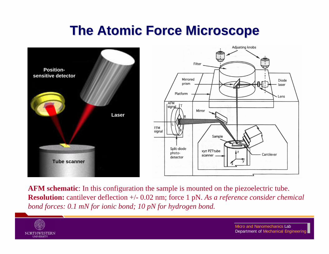
The Atomic Force MicroscopeThe Atomic Force Microscope
Laser
Tube scanner
Position-sensitive detector
AFM schematic: In this configuration the sample is mounted on the piezoelectric tube.Resolution: cantilever deflection +/- 0.02 nm; force 1 pN. As a reference consider chemical bond forces: 0.1 mN for ionic bond; 10 pN for hydrogen bond.

Micro and Nanomechanics LabDepartment of Mechanical Engineering
Patterning Molecular Inks at the Nanoscale

Micro and Nanomechanics LabDepartment of Mechanical Engineering
Dip-Pen Nanolithography (DPN)Direct-write nanopatterning technique based on AFM*.
Alkanethiolate molecules locally deposited on a Au surface.
REF: Science 283, 661 (1999)
AFM tip “nib” is used to deliver molecules “ink” to a surface “paper” via a solvent meniscus.
Feature size: ~10 nm – microns
*AFM: atomic force microscopy

Micro and Nanomechanics LabDepartment of Mechanical Engineering
Bio ApplicationsPresent and Future

Micro and Nanomechanics LabDepartment of Mechanical Engineering
DNA Arrays DNA Arrays ---- Gene Chip Gene Chip ---- BiochipsBiochips
APPLICATIONSAPPLICATIONS
•• Genetic Profiling (drug sideGenetic Profiling (drug sideeffects, allergies)effects, allergies)
•• Mutations indicative of Mutations indicative of diseasesdiseases
•• Cancer detection andCancer detection anddifferentiationdifferentiation
•• Drug DevelopmentDrug Development
•• Toxicology ExperimentsToxicology Experiments
•• Cell FunctionalityCell Functionality••

Micro and Nanomechanics LabDepartment of Mechanical Engineering
How Does It Work?How Does It Work?
Making Chips to Probe Genes, IEEE Spectrum, 2001

Micro and Nanomechanics LabDepartment of Mechanical Engineering
Identification of Active GenesIdentification of Active Genes• Single strand DNA array on Si or Glass
substrate• Binding of complementary sequences• Reading with fluorescent microscope• Analysis with computer software
Commercially Available!
Affimetrix

Micro and Nanomechanics LabDepartment of Mechanical Engineering
Surface Processing TechniquesSurface Processing Techniques
Patterns or spots of biological/chemical substances are deposited on surfaces to achieve a functionalized area for further processing (a bottom up approach).
Most current surface patterning methods are based on tools that are built using the top-down approach:− Ink-jet− Microcantilever spotters (miniaturized robot
spotting)− Scanning probe-based techniques− Soft lithography
Micro and Nanomechanics LabDepartment of Mechanical Engineering
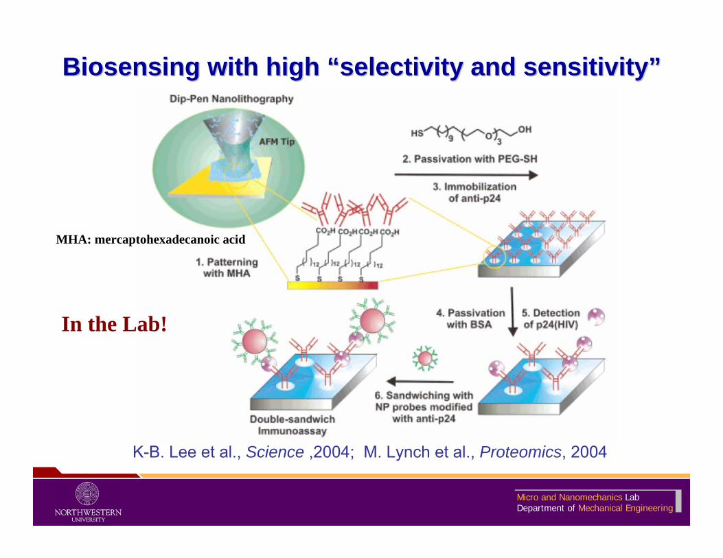
BiosensingBiosensing with high “selectivity and sensitivity”with high “selectivity and sensitivity”
MHA: mercaptohexadecanoic acid
In the Lab!
K-B. Lee et al., Science ,2004; M. Lynch et al., Proteomics, 2004

Micro and Nanomechanics LabDepartment of Mechanical Engineering
Cell Adhesion StudiesCell Adhesion Studies
A: Diagram describing the cell adhesion experiment on the DPN-generated pattern. The total patterned area is 6400 µm2. The alignment marks were generated by scratching a circle onto the backside of the Au-coated glass substrate.
B: Topography image (contact mode) of the RetronectinRetronectin protein array.
C: Large scale optical microscope image showing the localization localization of cellsof cells in the nanopatterned area
D: Higher resolution optical image of the nanopatterned area, showing intact cells
In the Lab!

Micro and Nanomechanics LabDepartment of Mechanical Engineering
Scaling Up the Patterning of Molecular Inks
at the Nanoscale

Micro and Nanomechanics LabDepartment of Mechanical Engineering
Contact-Based Surface ProcessingMicrocantilever spotter Fork-arm microcantilevers
REF: a) Belaubre et al., Appl. Phys. Lett. 2003, 14, 1472; b) Belaubre et al., Sens. Actuators A 2004, 110, 130
REF: Biomedical Microdevices 6, 117 (2004)
Feature size: ~10 µm to >100 µm Feature size: 2~3 µm
Robot spotter
REF: Reese et al., Genome. Res. 13, 2348 (2003)
1 mm
Feature size: > ~200 µm
Feature size: ~300 nm to 10 µm
REF: Lewis et al., Appl. Phys.Lett. 75, 2689 (1999);Bruckbauer et al., JACS 124, 8810 (2002)
Nanopipette
REF: Meister et al., Microelectron. Eng. 67-68, 644 (2003)
Feature size: >1 µm
Apertured AFM tip DPN
Feature size: <100 nm

Micro and Nanomechanics LabDepartment of Mechanical Engineering
2 µm
NanopipettesDPN
Parallelization
High resolution Continuous ink-feeding
High throughput
ObjectiveObjective
2 µm
Durability
Diamond tip
New device for surface processing

Micro and Nanomechanics LabDepartment of Mechanical Engineering
Three Evolutions of the NFP chipThree Evolutions of the NFP chip
500 nm
1 2 3
Micro and Nanomechanics LabDepartment of Mechanical Engineering
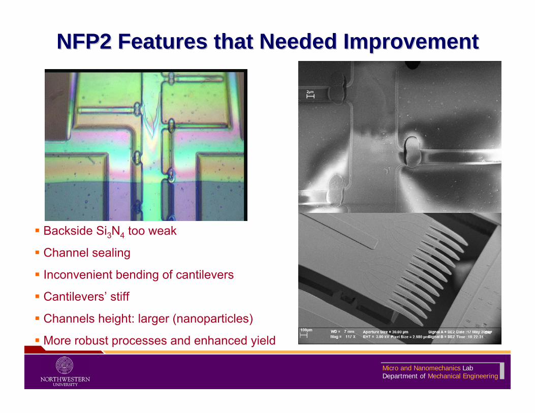
NFP2 Features that Needed ImprovementNFP2 Features that Needed Improvement
Backside Si3N4 too weak
Channel sealing
Inconvenient bending of cantilevers
Cantilevers’ stiff
Channels height: larger (nanoparticles)
More robust processes and enhanced yield

Micro and Nanomechanics LabDepartment of Mechanical Engineering
How it was improved: SOIHow it was improved: SOIThermal Oxidation, 0.5 µm
Litho M1 trench on backside + KOH (not shown)
Litho M2
Pyramid etch (KOH)
NHA etch
SiO2 removal (only 0.5 µm)
Litho M2’ (new mask)

Micro and Nanomechanics LabDepartment of Mechanical Engineering
SOI wafer (continued)SOI wafer (continued)SiO2 for sealing, PECVD, 2µm
Pattern sealing SiO2
Thick PR, backside litho, M6 (for lower contact) RIE to etch nitride Glue wafer onto another
DRIE: stop in SiO2
Remove glue (Nanostrip)

Micro and Nanomechanics LabDepartment of Mechanical Engineering
Second Generation NFP Chip
1
2
310 µm
500 nm
1 – reservoir, 2 – microchannels, 3 – volcano tip
Linear array of 12 cantilevers
Double-ink reservoirs
Elimination of sealing problems
Deep RIE release of chips (more chips per wafer)

Micro and Nanomechanics LabDepartment of Mechanical Engineering
NFP3
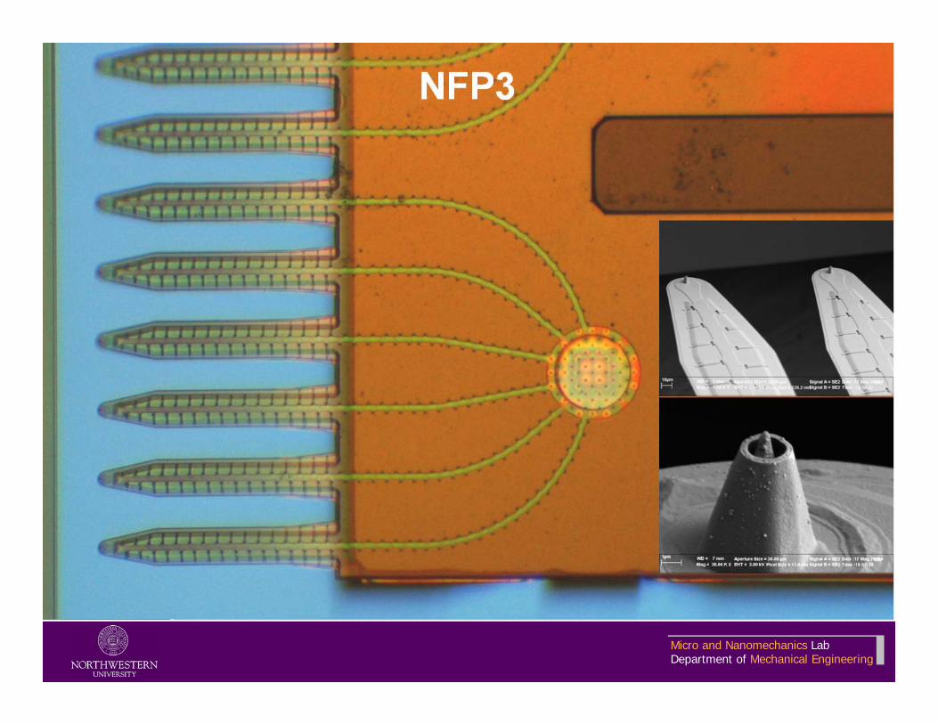
Micro and Nanomechanics LabDepartment of Mechanical Engineering
NFP3
Micro and Nanomechanics LabDepartment of Mechanical Engineering
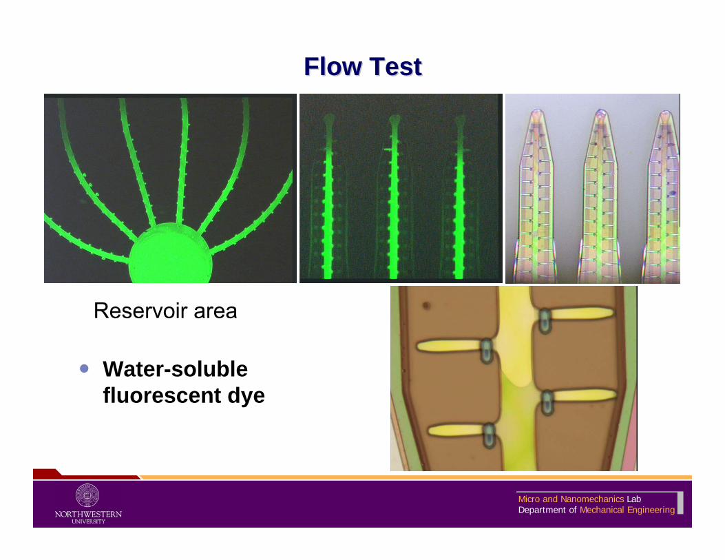
Flow TestFlow Test
Water-soluble fluorescent dye
Reservoir area

Micro and Nanomechanics LabDepartment of Mechanical Engineering
Comparison of Writing Mechanisms
Microelectron. Eng. 67-68, 644-650 (2003)Deposition of hexadecanethiols. Diameter: 10 µm
Controlled etch of chromium film. Linewidth ~1.45 µm
Appl. Phys.Lett. 75 (17), 2689 (1999)Feature size controlled by φ + α
Feature size controlled by R
Micro and Nanomechanics LabDepartment of Mechanical Engineering
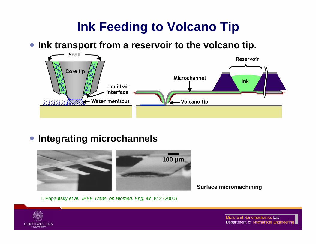
Ink Feeding to Volcano TipInk transport from a reservoir to the volcano tip.
100 µm
I. Papautsky et al., IEEE Trans. on Biomed. Eng. 47, 812 (2000)
Integrating microchannels
Surface micromachining
Micro and Nanomechanics LabDepartment of Mechanical Engineering
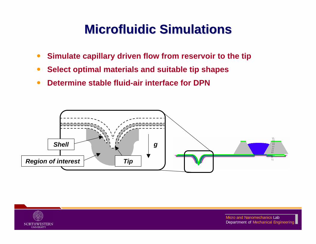
Microfluidic SimulationsMicrofluidic Simulations
Simulate capillary driven flow from reservoir to the tipSelect optimal materials and suitable tip shapesDetermine stable fluid-air interface for DPN
Region of interest
gShell
Tip

Micro and Nanomechanics LabDepartment of Mechanical Engineering
Ct= 20°, Cs= 65°
Microfluidic SimulationsMicrofluidic SimulationsFluid moves by capillary action from a reservoir to the end of a tipGood control of the equilibrium in fluid-air interface is obtained when the tip material is hydrophilic and the shell material is hydrophobic
Ct: contact angle on tip; Cs: contact angle on shellCt= 20°, Cs= 20°
Air
Fluid-air interface
Fluid(water)
1 µm
Tip(SiO2)
Shell(SiO2)
1 µm
Fluid-air interface
Air
Tip(Si3N4)
Shell(Si3N4)
Fluid(water)
Ct= 65°, Cs= 65°
Tip(SiO2)
Shell(Si3N4)
Air
Fluid(water)
1 µm
Fluid-air interface
Micro and Nanomechanics LabDepartment of Mechanical Engineering
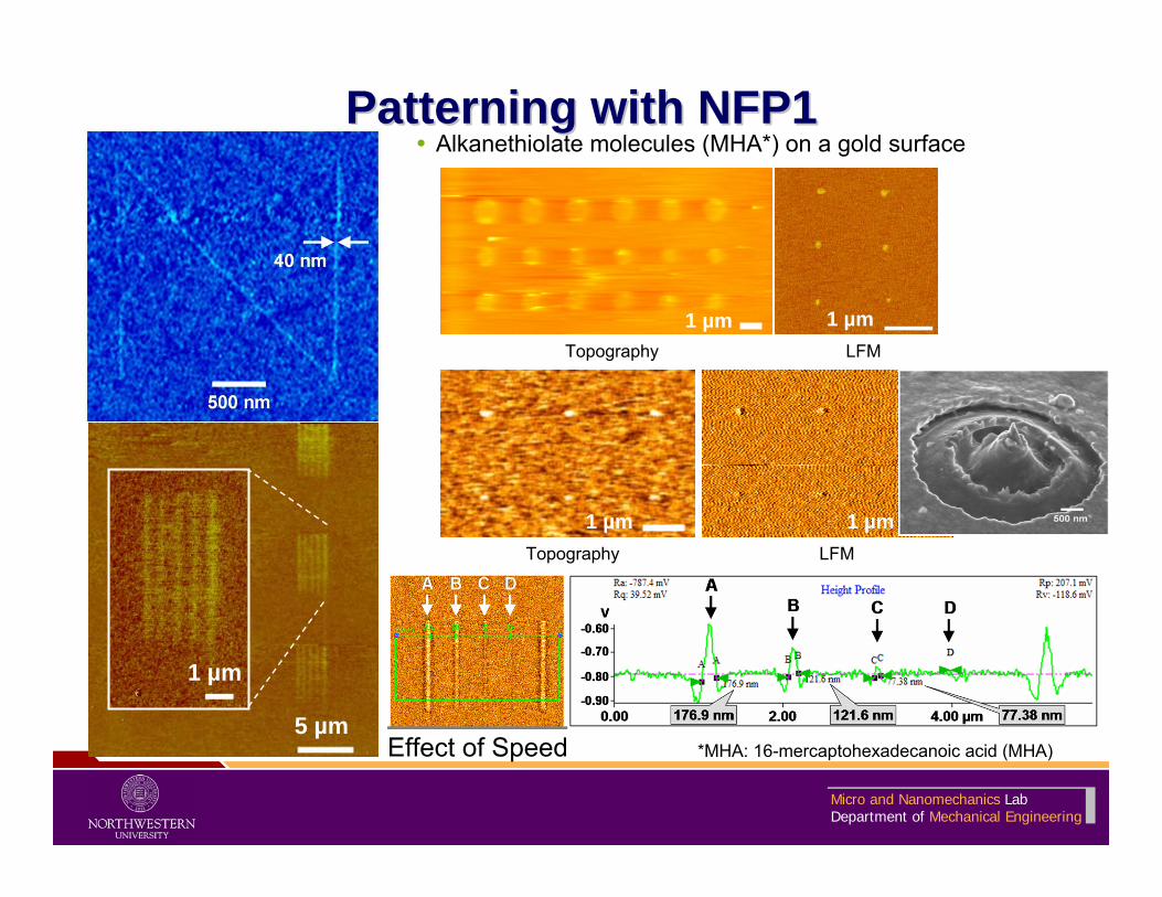
Patterning with NFP1Patterning with NFP1
5 µm
1 µm
Alkanethiolate molecules (MHA*) on a gold surface
LFMTopography
1 µm 1 µm
Topography
1 µmLFM
1 µm
*MHA: 16-mercaptohexadecanoic acid (MHA)Effect of Speed

Micro and Nanomechanics LabDepartment of Mechanical Engineering
MHA PFT
PFT (1H,1H,2H,2H-Perfluorododecane-1-thiol)CF3-CF2-(CF2)10-CH2-CH2-SH
NFP2: DoubleNFP2: Double--Ink PatterningInk PatterningSaturated solutions in acetonitrile of two different types of alkanethiols
MHAPFT
DNAs or proteins can be used as ink.
To appear JMM, 2006To appear JMM, 2006
Micro and Nanomechanics LabDepartment of Mechanical Engineering
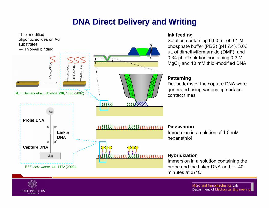
DNA Direct Delivery and WritingDNA Direct Delivery and WritingInk feedingSolution containing 6.60 µL of 0.1 M phosphate buffer (PBS) (pH 7.4), 3.06 µL of dimethylformamide (DMF), and 0.34 µL of solution containing 0.3 M MgCl2 and 10 mM thiol-modified DNA
PatterningDot patterns of the capture DNA were generated using various tip-surface contact times
PassivationImmersion in a solution of 1.0 mM hexanethiol
Capture DNA
Probe DNA
Linker DNA
REF: Adv. Mater. 14, 1472 (2002)
HybridizationImmersion in a solution containing the probe and the linker DNA and for 40 minutes at 37°C.
REF: Demers et al., Science 296, 1836 (2002)
Thiol-modified oligonucleotides on Au substrates→ Thiol-Au binding
Micro and Nanomechanics LabDepartment of Mechanical Engineering
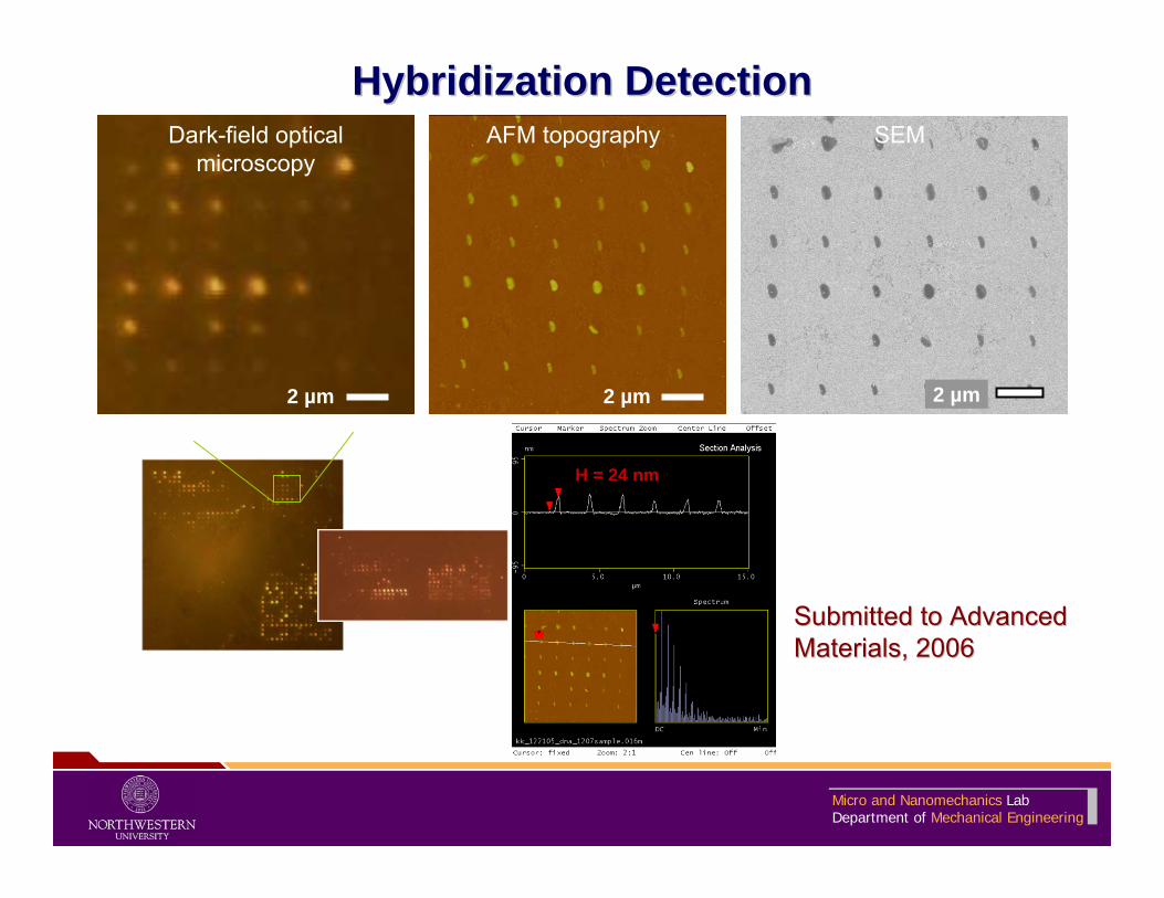
2 µm 2 µm 2 µm
Dark-field optical microscopy
AFM topography SEM
Hybridization DetectionHybridization Detection
H = 24 nm
Submitted to Advanced Submitted to Advanced Materials, 2006Materials, 2006

Micro and Nanomechanics LabDepartment of Mechanical Engineering
Hybridization DetectionHybridization Detection
Micro and Nanomechanics LabDepartment of Mechanical Engineering
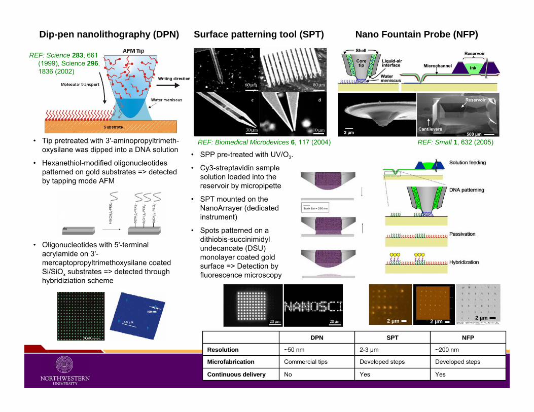
Dip-pen nanolithography (DPN) Surface patterning tool (SPT) Nano Fountain Probe (NFP)
Yes
Developed steps
~200 nm
NFPNFP
Yes
Developed steps
2-3 µm
SPTSPT
No
Commercial tips
~50 nm
DPNDPN
Continuous deliveryContinuous delivery
MicrofabricationMicrofabrication
ResolutionResolution
• SPP pre-treated with UV/O3.
• Cy3-streptavidin sample solution loaded into the reservoir by micropipette
• SPT mounted on the NanoArrayer (dedicated instrument)
• Spots patterned on a dithiobis-succinimidylundecanoate (DSU) monolayer coated gold surface => Detection by fluorescence microscopy
• Tip pretreated with 3'-aminopropyltrimeth-oxysilane was dipped into a DNA solution
• Hexanethiol-modified oligonucleotides patterned on gold substrates => detected by tapping mode AFM
• Oligonucleotides with 5'-terminal acrylamide on 3'-mercaptopropyltrimethoxysilane coated Si/SiOx substrates => detected through hybridiziation scheme
2 µm 2 µm 2 µm
REF: Science 283, 661 (1999), Science 296, 1836 (2002)
REF: Biomedical Microdevices 6, 117 (2004) REF: Small 1, 632 (2005)
Micro and Nanomechanics LabDepartment of Mechanical Engineering
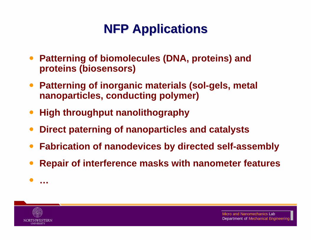
NFP ApplicationsNFP Applications
Patterning of biomolecules (DNA, proteins) and proteins (biosensors)
Patterning of inorganic materials (sol-gels, metal nanoparticles, conducting polymer)
High throughput nanolithography
Direct paterning of nanoparticles and catalysts
Fabrication of nanodevices by directed self-assembly
Repair of interference masks with nanometer features
…
Micro and Nanomechanics LabDepartment of Mechanical Engineering
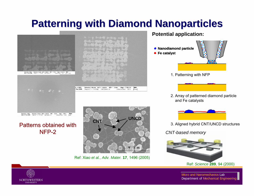
Patterning with Diamond NanoparticlesPatterning with Diamond Nanoparticles
Ref: Xiao et al., Adv. Mater. 17, 1496 (2005)
UNCDCNT 3. Aligned hybrid CNT/UNCD structures
Nanodiamond particleFe catalystNanodiamond particleFe catalyst
1. Patterning with NFP
2. Array of patterned diamond particle and Fe catalysts
Potential application:
CNT-based memory
Ref: Science 289, 94 (2000)
Patterns obtained withPatterns obtained withNFPNFP--22
Micro and Nanomechanics LabDepartment of Mechanical Engineering
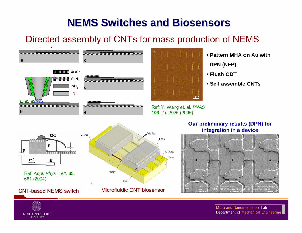
NEMS NEMS Switches and BiosensorsSwitches and BiosensorsDirected assembly of CNTs for mass production of NEMS
devices
Ref: Appl. Phys. Lett. 85, 681 (2004)
CNTCNT--based NEMS switchbased NEMS switch
Ref: Y. Wang et. al. PNAS103 (7), 2026 (2006)
• Pattern MHA on Au with
DPN (NFP)
• Flush ODT
• Self assemble CNTs
MicrofluidicMicrofluidic CNT biosensorCNT biosensor
Our preliminary results (DPN) for integration in a device

Micro and Nanomechanics LabDepartment of Mechanical Engineering
11--D Array with Multiple InksD Array with Multiple Inks
Micro and Nanomechanics LabDepartment of Mechanical Engineering
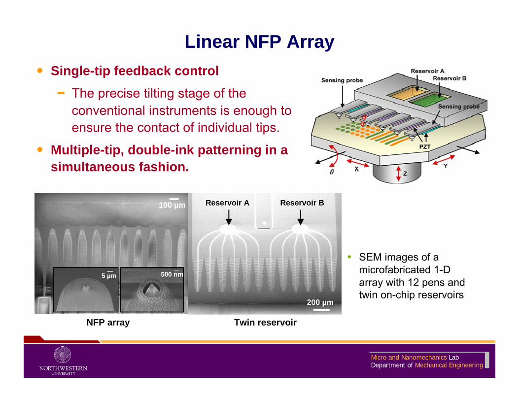
Linear NFP ArraySingle-tip feedback control− The precise tilting stage of the
conventional instruments is enough to ensure the contact of individual tips.
Multiple-tip, double-ink patterning in a simultaneous fashion.
NFP array Twin reservoir
100 µm
5 µm 500 nm
200 µm
Reservoir A Reservoir B
SEM images of a microfabricated 1-D array with 12 pens and twin on-chip reservoirs
Micro and Nanomechanics LabDepartment of Mechanical Engineering
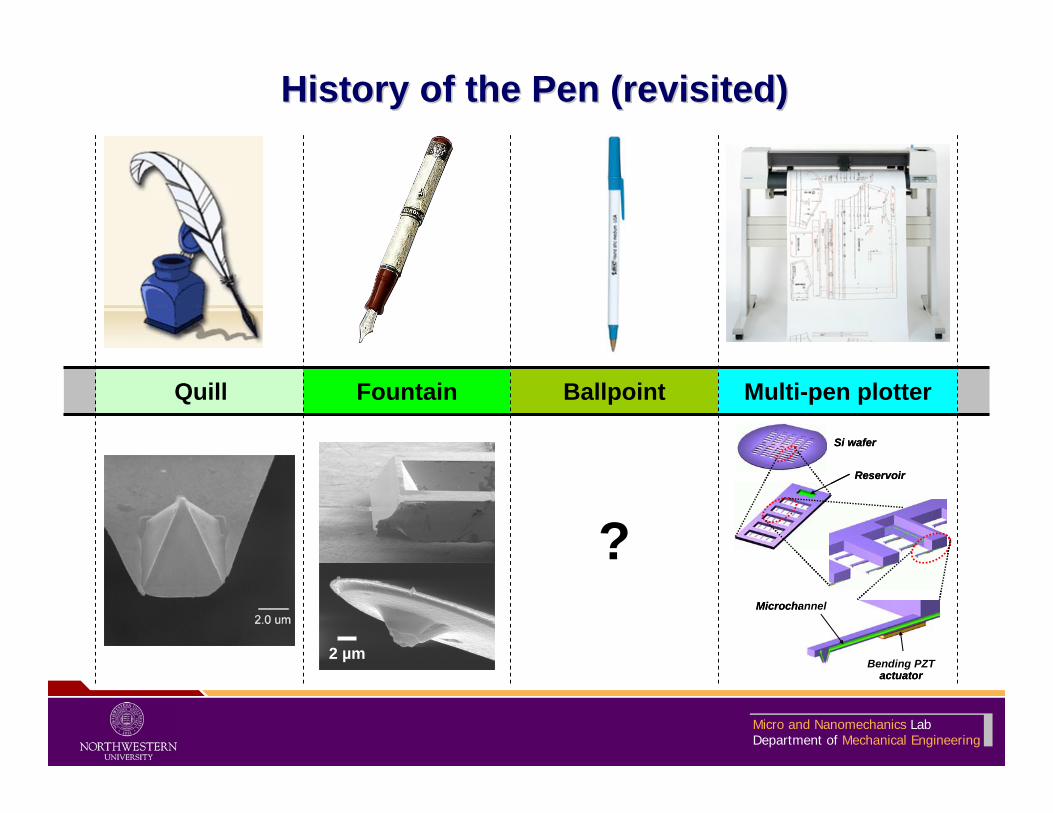
History of the Pen (revisited)History of the Pen (revisited)
?
Si wafer
Reservoir
Bending PZT actuator
Microchannel
Si wafer
Reservoir
Bending PZT actuator
Microchannel
Quill Fountain Ballpoint Multi-pen plotter
2 µm
Micro and Nanomechanics LabDepartment of Mechanical Engineering
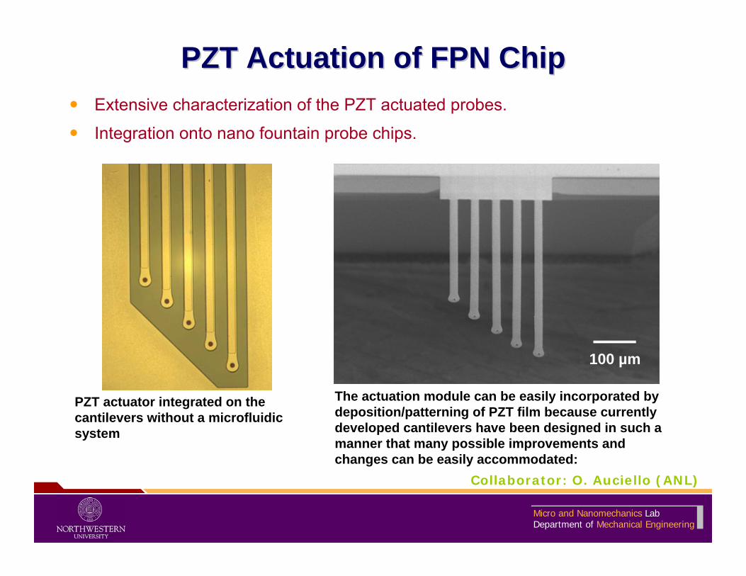
PZT Actuation of FPN ChipPZT Actuation of FPN ChipExtensive characterization of the PZT actuated probes.
Integration onto nano fountain probe chips.
100 µm
PZT actuator integrated on the cantilevers without a microfluidic system
The actuation module can be easily incorporated by deposition/patterning of PZT film because currently developed cantilevers have been designed in such a manner that many possible improvements and changes can be easily accommodated:
Collaborator: O. Auciello (ANL)
Micro and Nanomechanics LabDepartment of Mechanical Engineering
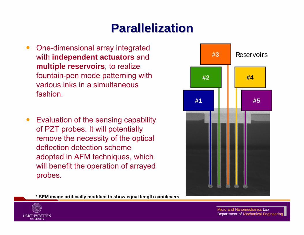
ParallelizationParallelizationOne-dimensional array integrated with independent actuators and multiple reservoirs, to realize fountain-pen mode patterning with various inks in a simultaneous fashion.
Evaluation of the sensing capability of PZT probes. It will potentially remove the necessity of the optical deflection detection scheme adopted in AFM techniques, which will benefit the operation of arrayed probes.
#1
#2
#3
#4
#5
Reservoirs
* SEM image artificially modified to show equal length cantilevers

Micro and Nanomechanics LabDepartment of Mechanical Engineering
PZT ActuationPZT ActuationIntegration of PZT actuators with AFM cantilevers without microfluidic system.
Optical image of the cantilevers with PZT actuators and electrodes prior to release
Bottom electrode
Top electrodes
Micro and Nanomechanics LabDepartment of Mechanical Engineering
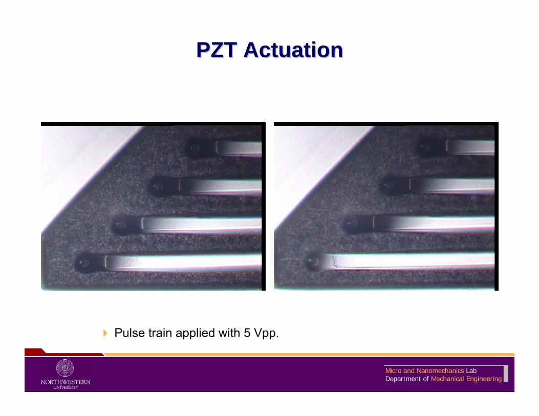
PZT ActuationPZT Actuation
Pulse train applied with 5 Vpp.

Micro and Nanomechanics LabDepartment of Mechanical Engineering
Bending Profile of the CantileversBending Profile of the CantileversQuantitative evaluation with phase shift technology.
6
4
2
0
-2
Hei
ght (
µm)
8006004002000x (µm)
0V 3V 4.5V 5V
4 µm
Micro and Nanomechanics LabDepartment of Mechanical Engineering
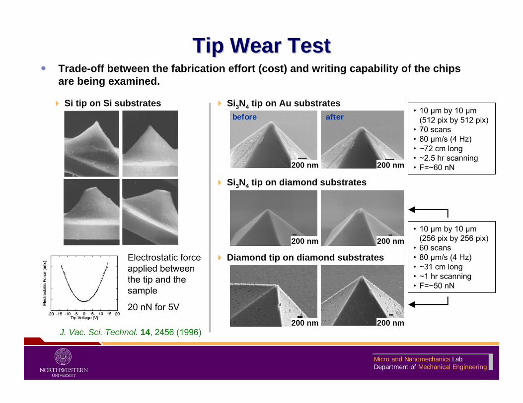
Tip Wear TestTip Wear TestTrade-off between the fabrication effort (cost) and writing capability of the chips are being examined.
J. Vac. Sci. Technol. 14, 2456 (1996)
Si tip on Si substrates
200 nm 200 nm
200 nm 200 nm
200 nm200 nm
Si3N4 tip on Au substrates
Si3N4 tip on diamond substrates
Diamond tip on diamond substrates
• 10 µm by 10 µm (512 pix by 512 pix)
• 70 scans• 80 µm/s (4 Hz)• ~72 cm long• ~2.5 hr scanning• F=~60 nN
• 10 µm by 10 µm (256 pix by 256 pix)
• 60 scans• 80 µm/s (4 Hz)• ~31 cm long• ~1 hr scanning• F=~50 nN
Electrostatic force applied between the tip and the sample
20 nN for 5V
before after

Micro and Nanomechanics LabDepartment of Mechanical Engineering
Diamond AFM ProbeL~100-500 µm
UNCD*doped to be conductive
h~3-7 µm
10 µm
Molding technique for ultra-sharp tip fabrication
images of a microfabricated probes
*UNCD: Ultrananocrystalline Diamond, grain size 2-5 nm
(b)
Micro and Nanomechanics LabDepartment of Mechanical Engineering
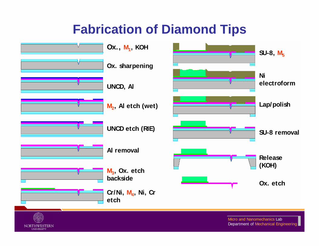
Fabrication of Diamond TipsOx., M1, KOH
SU-8, M5
Ox. sharpening
UNCD, Al
M2, Al etch (wet)
UNCD etch (RIE)
Al removal
M3, Ox. etch backside
Cr/Ni, M4, Ni, Cr etch
Ni electroform
Lap/polish
SU-8 removal
Release (KOH)
Ox. etch

Micro and Nanomechanics LabDepartment of Mechanical Engineering
DPN CompatibilityDPN compatibility has been examined with diamond tips.
1 µm
LFM image of patterned letters by the diamond probe

Micro and Nanomechanics LabDepartment of Mechanical Engineering
Conduction Map
Topography Conduction Map
Scanned Region

Micro and Nanomechanics LabDepartment of Mechanical Engineering
UNCD Tip CharacterizationContact Resistance: 6.25 kΩ
AFM Potentiometry
Micro and Nanomechanics LabDepartment of Mechanical Engineering
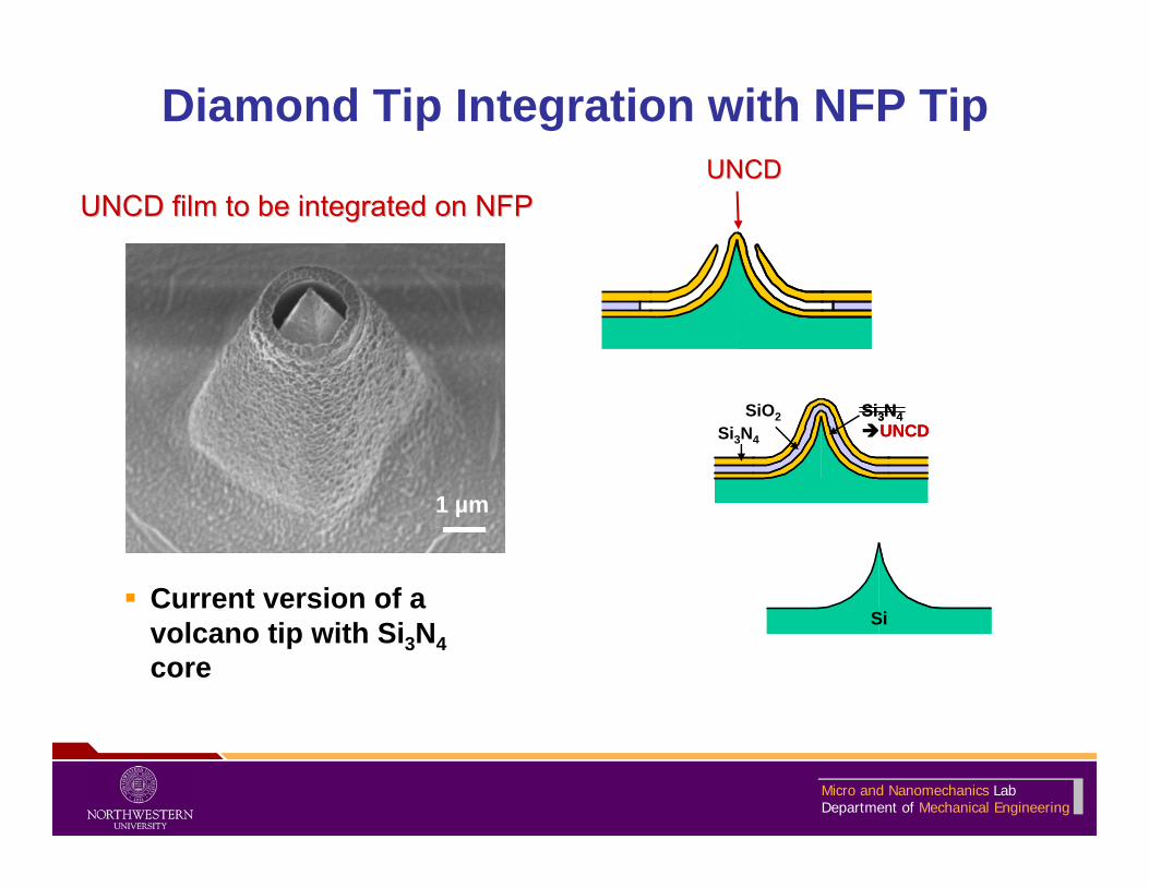
Diamond Tip Integration with NFP Tip
UNCD film to be integrated on NFPUNCD film to be integrated on NFP
Si
UNCDUNCD
SiO2Si3N4
Si3N4UNCD
Si3N4UNCD
1 µm
Current version of a volcano tip with Si3N4core