microelectronics industry energy efficiency initiative
TRANSCRIPT

Microelectronics Industry Energy Efficiency Initiative M a r k e t P r o g r e s s E v a l u a t i o n R e p o r t , N o . 2
prepared by
Research Into Action, Inc.
report #E03-117
June 26, 2003
529 SW Third Avenue, Suite 600 Portland, Oregon 97204 telephone: 503.827.8416 fax: 503.827.8437

Final Report
SECOND MARKET PROGRESS EVALUATION REPORT OF THE MICROELECTRONICS INITIATIVE
Funded By:
Submitted To:
Phil Degens Northwest Energy Efficiency Alliance
Prepared By:
Jane S. Peters, Ph.D. Marjorie R. McRae, Ph.D.
Research Into Action, Inc.
Steven Scott, P.E. MetaResource Group
3% Energy Efficiency 27% Product Awareness 57% Customer Satisfaction 74% Market Share
Market Potential 72% Consumer Confidence 46% Brand Recognition 82% Energy Savings 69% Market Penetration 6

MICROELECTRONICS INITIATIVE – MPER #2
ACKNOWLEDGEMENTS
We would like to thank Phil Degens of the Alliance for his guidance and support throughout this project and Michael Ponder of the Alliance for his cooperation as we proceeded in the project.
We also want to acknowledge George Burns of Strategic Marketing Associates and Doug Barrett of Colliers International for their assistance providing us with valuable insights on the current state and future prospects of semiconductor fabrication facilities in the Pacific Northwest.
We could not have completed this work without the willingness of industry members to respond to our requests for interview time. Therefore, we would like to thank all of the participants in special projects and Microelectronics workshops for their cooperation in this project.

Acknowledgements
MICROELECTRONICS INITIATIVE – MPER #2

MICROELECTRONICS INITIATIVE – MPER #2 PAGE I
TABLE OF CONTENTS
EXECUTIVE SUMMARY....................................................................................................................I
1. INTRODUCTION.........................................................................................................................1 INITIATIVE DESCRIPTION ..................................................................................................1 FINDINGS FROM MPER 1....................................................................................................3
The CRA Microelectronics Initiative............................................................................6 The Special Project Fund............................................................................................7 Recommendations.......................................................................................................8
STRUCTURE OF THIS MPER............................................................................................. 10
2. WORKSHOP PARTICIPANTS ....................................................................................................12 INTRODUCTION ................................................................................................................ 12
Description of Activities ............................................................................................ 12 Study Approach........................................................................................................ 12
FINDINGS .......................................................................................................................... 14 Participation ............................................................................................................ 14 Value and Influence of Workshops............................................................................. 15 Design Guidelines..................................................................................................... 20 Alliance Influence on Industry .................................................................................. 21
SUMMARY .......................................................................................................................... 22
3. SPECIAL PROJECTS .................................................................................................................23 DESCRIPTION OF THE SPECIAL PROJECTS.................................................................... 23
Manufacturer – Hewlett-Packard / Consultant – EN-WISE........................................ 23 Manufacturer – Intel / Consultant – Willis Energy Services ....................................... 26 Manufacturer – Zilog/ Consultant – Supersymmetry.................................................. 28
PROCESS ISSUES............................................................................................................... 29 BARRIERS........................................................................................................................... 30
4. H-P DESIGN CHARETTE ...........................................................................................................33 INTRODUCTION ................................................................................................................ 33
Description of Project................................................................................................ 33 Study Approach........................................................................................................ 34

Table of Contents
MICROELECTRONICS INITIATIVE – MPER #2 PAGE I I
THE CHARETTE................................................................................................................. 34 Constraints to Energy Efficient Design...................................................................... 35 Results from the Idea Generation .............................................................................. 36
FOLLOW-UP INTERVIEWS................................................................................................ 36 Overall Impressions of the Charette .......................................................................... 37 Changes to Fab Design ............................................................................................. 39
SUMMARY .......................................................................................................................... 42
5. DENDRITIC POLYSILICON PRODUCTION .............................................................................43 STUDY APPROACH ............................................................................................................ 43 PROJECT HISTORY............................................................................................................ 43
Project Initiation ...................................................................................................... 44 Market Transformation Theory................................................................................. 44 Project Progress ....................................................................................................... 45
ASSESSMENT OF PROJECT PROGRESS............................................................................ 46 Impact of the Joint Venture and Production in Butte ................................................. 46 Other Market Issues................................................................................................. 46
NEXT STEPS FOR THE EVALUATION .............................................................................. 48 TECHNICAL SECTION ....................................................................................................... 49
Teardrop Polycrystalline Silicon ................................................................................ 49 Energy Benefits of Teardrop...................................................................................... 50 Description of Recharge Methods............................................................................... 51
6. PERSPECTIVES ON THE MICROELECTRONICS INDUSTRY....................................................54 CURRENT INDUSTRY CONDITIONS................................................................................. 54 INDUSTRY CHANGES IN THE PAST THREE YEARS........................................................ 55 FUTURE TRENDS .............................................................................................................. 57 MARKET LEADERS ............................................................................................................ 58 BARRIERS AND OPPORTUNITIES..................................................................................... 58
7. MARKET ASSESSMENT.............................................................................................................62 INTRODUCTION ................................................................................................................ 62
Description of Approach ............................................................................................ 63 Description of Analysis ............................................................................................. 64
ANALYSIS RESULTS.......................................................................................................... 66

Table of Contents
MICROELECTRONICS INITIATIVE – MPER #2 Page III
FINDINGS .......................................................................................................................... 70 Historical Trends ..................................................................................................... 70 Market Trends ......................................................................................................... 73 Location Choice Drivers............................................................................................ 75 Outlook for 2004....................................................................................................... 76 Outlook for 2007....................................................................................................... 77
COST-EFFECTIVENESS RECOMMENDATIONS................................................................. 78 Introduction ............................................................................................................. 78 Cost-Effectiveness Assumptions and Recommendations .............................................. 78
Project Size & Facility Energy Use...........................................................................................79 Number of Facilities ....................................................................................................................80 Initiative & Market Effect Projects ..........................................................................................80 Capital Costs.................................................................................................................................80 Operation and Maintenance Costs...........................................................................................81 Lifetime of Measure.....................................................................................................................81 Efficiency Improvement ...............................................................................................................81 Non-Energy Benefits ....................................................................................................................81 Program Expenditures.................................................................................................................81
8. FINDINGS AND RECOMMENDATIONS.................................................................................83
APPENDICES APPENDIX A: INTERVIEW GUIDE FOR MICROELECTRONICS INITIATIVE
ALLIANCE WORKSHOPS .............................................................................................A-1 APPENIDX B: INTERVIEW GUIDE FOR MICROELECTRONICS INITIATIVE
EXPLORATION OF SPECIAL PROJECTS .....................................................................B-1 APPENDIX C: INTERVIEWS FOR H-P DESIGN CHARETTE............................................C-1

Table of Contents
MICROELECTRONICS INITIATIVE – MPER #2 PAGE IV

MICROELECTRONICS INITIATIVE – MPER #2 PAGE I
EXECUTIVE SUMMARY
The Northwest Energy Efficiency Alliance (the Alliance) is a non-profit group of electric utilities, state governments, public interest groups and industry representatives committed to bringing affordable, energy-efficient products and services to the marketplace. The Alliance sponsors the Microelectronics Initiative (the Initiative), which has a variety of components.
The Initiative was begun in 1997, during the first year of Alliance operation. Its initial efforts focused on outreach to the microelectronics industry, meetings to familiarize this sector with energy efficient approaches, contact with potential solution-providers, and a willingness to fund special projects that could demonstrate energy efficient solutions and advance the market awareness and interest in them.
In addition to this targeted effort, the Alliance has funded other projects in the broad microelectronics industry, including a project with Siemens Solar—now Shell Solar—that also began in 1997. This project involved efforts to improve the energy efficiency of production furnaces used for manufacturing crystalline silicon for photovoltaic applications.
The Initiative now includes a spectrum of approaches beyond the initial market investigation projects proposed by Chris Robertson & Associates, LLC (CRA) and Shell Solar, and the dissemination activities supported by the Alliance. Current efforts include:
Ø Three Special Fund projects for the demonstration and benchmarking of energy savings opportunities in chilled water plants at semiconductor fabrication facilities—two identified by CRA and one submitted in response to a request for proposals by the Alliance;
Ø Co-funding for a project by Lawrence Berkeley National Laboratories (LBNL) to develop design guidelines for cleanrooms;
Ø A series of workshops sponsored by the Alliance (three to date), which bring national and regional experts in energy efficiency for the microelectronics industry to make presentations to regional microelectronics firms and engage in discussions about additional opportunities;

Executive Summary
MICROELECTRONICS INITIATIVE – MPER #2 PAGE II
Ø A research effort to understand opportunities for energy efficiency improvements in polysilicon manufacturing; and
Ø New projects that have emerged from the first projects and have been integrated into the Microelectronics Initiative, including:
• The ASiMI Dendritic Polysilicon Production project to develop a smaller-sized polysilicon product that is both more energy efficient to produce and can be more easily used in recharge applications, reducing energy consumption for the product user;
• The H-P Design Charette to identify energy efficient retrofit opportunities for implementation in the renovation of an existing semiconductor fabrication (fab) facility;
• The Industrial Design & Construction (IDC) Energy Efficient Fab Design Charette, to identify energy efficient opportunities for a generic new fabrication facility;
• A pending process tool design charette;
• The pending Aketon, energy efficient tool emissions abatement project; and
• Other project ideas currently being discussed with local microelectronics firms that may result in additional projects for the Initiative.
Several of these efforts are the focus of this evaluation. The first is the Special Project Fund for workshop, demonstration and benchmarking projects focusing on Pacific Northwest (PNW) microelectronics firms; second are the workshops and the LBNL design guidelines that emerged; the third is the Hewlett-Packard (H-P) Design Charette; and the fourth is the Dendritic Polysilicon Production project. In addition, this report provides an updated market assessment, focusing on the PNW market for semiconductor fabrication and cleanroom facilities. This Market Progress Evaluation Report (MPER) is the second evaluation report for the Initiative.
The results of this evaluation effort confirm that the Alliance efforts with the Microelectronics Initiative are having a positive effect on the industry. Among the most effective activities have been the workshops, which we strongly recommend that the Alliance continue on an annual basis.

Executive Summary
MICROELECTRONICS INITIATIVE – MPER #2 Page III
The other significant finding from the evaluation is that the growth of semiconductor fabrication facilities has slowed substantially since 1995. At the same time, we also found that the assumptions the Alliance used for estimating program impacts assumed the facilities were much smaller than they actually are. In addition, we noted substantial growth in the construction of cleanrooms by other industries, although with less stringent requirements for air and water purity, nonetheless suggesting that there is an overall concern with the energy issues associated with cleanrooms throughout the region. We provide recommendations here both for program expansion and for fine-tuning the cost effectiveness estimates for the Initiative.
Overall, six conclusions and recommendations emerge from this MPER effort. They are briefly discussed below.
Finding 1
The workshops sponsored by the Alliance, are a very effective market transformation tool. This is backed by strong evidence from workshop attendees and from the fact that two of the three special fund projects and the H-P design charette emerged in large part as a result of the firms’ experience with the workshops.
Recommendation 1
Continue offering one workshop per year.
Finding 2
The Special Projects Fund approach has identified and implemented a significant number of energy efficiency measures in semiconductor fabs. Although the availability of funding from the Alliance was an attraction to undertake the special projects, the implemented measures were no-cost and low-cost, and many have achieved substantial energy savings.
Recommendation 2
The Alliance should move to quickly publicize the results from the Special Projects Fund efforts, both in workshops and as case studies reports.

Executive Summary
MICROELECTRONICS INITIATIVE – MPER #2 PAGE IV
Finding 3
The H-P design charette was extremely effective in achieving specific savings for the plant and in influencing internal behavior to consider energy efficiency ideas, such as design charettes, for future projects.
Recommendation 3
Charettes can provide an effective means to influence plant design and the Alliance should continue to pursue this approach.
Finding 4
The ASiMI project at Moses Lake, Washington, and at Butte, Montana, appears to provide a clear example of local energy conservation. The market transformation effects appear to be limited. This is both because of the joint venture, which splits ASiMI production into either solar grade or semiconductor grade, and the fact that at this time neither grade appears likely to result in changes in recharge behavior on the part of the semiconductor industry, where the greatest savings are possible. In addition, the current industry slump is not conducive to firms doing more than exploring their options so no changes in behavior are likely to occur until the industry rebounds.
Recommendation 4
Continue to monitor industry response to the ASiMI products—teardrop and teardrop plus.
Finding 5
The market assessment uncovered a large potential common market in cleanrooms in microelectronics and other industries, such as biomedical, pharmaceutical and other electronic sectors. Reaching all regarding efficiency in cleanrooms may improve opportunities in the microelectronics industry itself and will spread the affects of the Initiative more widely to the region.
Recommendation 5

Executive Summary
MICROELECTRONICS INITIATIVE – MPER #2 Page V
Consider exploring the common aspect of cleanrooms and solutions for improving the energy efficiency of all as a market transformation opportunity for multiple industries.
Finding 6
There are some indications that energy efficiency may play a small part in decisions to purchase semiconductor fabs. With investments in new PNW fabs over the next few years being limited, there may be opportunity to affect efficiency change when existing facilities are turned over to new ownership.
Recommendation 6
Consider the opportunity of marketing energy impacts and efficiency for selection of closed or for sale microelectronics facilities.

Executive Summary
MICROELECTRONICS INITIATIVE – MPER #2 PAGE VI

MICROELECTRONICS INITIATIVE – MPER #2 PAGE 1
1. INTRODUCTION
The Northwest Energy Efficiency Alliance (the Alliance) is a non-profit group of electric utilities, state governments, public interest groups and industry representatives committed to bringing affordable, energy-efficient products and services to the marketplace. The Alliance sponsors the Microelectronics Initiative (the Initiative), which has a variety of components. Four are the focus of this evaluation. The first is the Special Project Fund for workshop, demonstration and benchmarking projects focusing on Pacific Northwest (PNW) microelectronics firms; second are the workshops and the LBNL design guidelines; the third is the Hewlett-Packard (H-P) Design Charette; and the fourth is the Dendritic Polysilicon Production project. In this chapter, we describe the various aspects of the initiative and introduce the evaluation. This Market Progress Evaluation Report (MPER) is the second evaluation report for the Initiative.
INITIATIVE DESCRIPTION
The Alliance held an open solicitation for market transformation projects in the spring of 1997. In response, Chris Robertson & Associates, LLC (CRA) submitted a proposal requesting support for efforts to "identify early adopters, help them to explore advanced resource efficiency and then present their examples to other firms in the industry." As part of this effort, CRA also requested funds be available for use in supporting viable projects that could demonstrate the value of energy efficiency efforts. The crux of the proposal by CRA was to focus on early adopters, which were not necessarily firms located in the PNW. The premise was that the microelectronics industry is global and tends to follow the leaders, thus when early adopters accept a new idea, the rest of the industry will follow.
The Initiative was funded at $1.43 million for a two-year effort. Approximately 50% was allocated to a Special Projects fund, which was placed in reserve for allocation by Alliance staff under the direction of the Board of Directors. CRA was hired to identify and contact early adopters, and the Alliance hired a staff person to oversee the project, conduct workshops with industry representatives in the PNW and oversee

1. Introduction
MICROELECTRONICS INITIATIVE – MPER #2 PAGE 2
the Special Projects Fund. The first Microelectronics MPER discusses the first three years of these efforts.1
Siemens Solar, now Shell Solar, also proposed a project in 1997. This project involved efforts to improve the energy efficiency of silicon crystal growing production furnaces used for manufacturing crystalline silicon for photovoltaic applications. Shell asked for funding to increase the energy efficiency of their production process. Over three years they improved this process and reduced energy consumption by 51% per run, for annual estimated savings of 2,000,000 kWh.
The market transformation goal was to publicize the success of the Shell project in order to inspire and encourage the adoption of energy efficiency solutions by silicon crystal producers for semiconductor chip manufacturing. This project is reported on in two other MPERs and is now being monitored as part of the Microelectronics Initiative, although the follow-on monitoring is not discussed in this MPER.2
Since 1997, several other projects have developed. Figure 1 displays the evolution as of fall 2002. The figure shows how the Microelectronics Initiative now includes a spectrum of efforts beyond the initial market investigation projects proposed by CRA and Shell Solar and the dissemination activities supported by the Alliance. These include:
Ø Three projects for demonstration and benchmarking of energy savings opportunities in the chilled water plants at semiconductor fabrication facilities, two identified by CRA and one submitted in response to a request for proposals by the Alliance;
Ø Co-funding for a project by Lawrence Berkeley National Laboratories (LBNL) to develop design guidelines for cleanrooms;
Ø A series of workshops sponsored by the Alliance (three to date), which bring national and regional experts in energy efficiency for the microelectronics
1 Peters, Jane S., Marjorie McRae and Shel Feldman (2001) First Market Progress Evaluation Report of the Microelectronics Initiative, (E01-089), Northwest Energy Efficiency Alliance.
2 Peters, Jane S. and Shel Feldman (2001) Silicon Crystal Growing Facilities: Market Progress Evaluation Report #2, (E 01-090), Northwest Energy Efficiency Alliance. Reed, John H., Andrew D. Oh and Nicholas P. Hall (1999). Market Progress Evaluation Report: Silicon Crystal Growing Facilities, No. 1, (E99-034), Northwest Energy Efficiency Alliance.

1. Introduction
MICROELECTRONICS INITIATIVE – MPER #2 Page 3
industry to make presentations to regional microelectronics firms and engage in discussions about additional opportunities;
Ø A research effort to understand opportunities for energy efficiency improvements in polysilicon manufacturing; and
Ø New projects that have emerged from the first projects and have been integrated into the Microelectronics Initiative, including:
• The ASiMI Dendritic Polysilicon Production project to develop a smaller-sized polysilicon product that is both more energy efficient to produce and can be more easily used in recharge applications, reducing energy consumption for the product user;
• The H-P Design Charette to identify energy efficient retrofit opportunities for implementation in the renovation of an existing semiconductor fabrication (fab) facility;
• The Industrial Design & Construction (IDC) Energy Efficient Fab Design Charette, to identify energy efficient opportunities for a generic new fabrication facility;
• A pending process tool design charette;
• The pending Aketon energy-efficient tool emissions abatement project; and
• Other project ideas currently being discussed with local microelectronics firms that may result in additional projects for the Initiative.
FINDINGS FROM MPER 1
The first Market Progress Evaluation Report focused on two activities of the Initiative. The first: a contract with Chris Robertson & Associates, LLC that the Alliance funded from 1997 to 1999. The second: the Special Project Fund for demonstration and benchmarking projects and workshops conducted by the Alliance to reach out to Pacific Northwest microelectronics firms.
The Microelectronics Industry is first and foremost a manufacturing industry. The decision-making processes in the industry are similar to other industries, project

1. Introduction
MICROELECTRONICS INITIATIVE – MPER #2 PAGE 4
champions are important in project development and implementation and groups of decision-makers are the rule, rather than the exception. It is, however, different from other manufacturing industries with which the Alliance is familiar.

1. Introduction
MICROELECTRONICS INITIATIVE – MPER #2 PAGE 5
Figure 1
EVOLUTION OF THE MICROELECTRONICS INITIATIVE
Siemens/ Shell
Proposal
A L L I ANCE
PROCESS TECHNOLOGY
SIEMENS HOT TOP-OFF POLYSILICON
RESEARCH
CHILLED WATER DEMO
OPTICHILL H-P
ZILOG
CLEAN ROOMS
LBNL DESIGN GUIDE
DISSEMINA-TION
WORKSHOPS
PUBLICATIONS
FORUMS
MARKET INVESTIGATION
INDUSTRY MEETINGS SOLUTION PROVIDER
PROPOSALS
OptiChill Proposal
CRA Proposal
ASiMI Proposal
PROCESS TECHNOLOGY
DENDRYTIC POLYSILICON PRODUCTION
CLEAN ROOM
H-P DESIGN CHARETTE
IDC Proposal
H-P Proposal
CLEAN ROOM
PROCESS TOOL CHARETTE
ENERGY EFFICIENT FAB
CHARETTE
A L L I ANCE
A L L I ANCE

1. Introduction
MICROELECTRONICS INITIATIVE – MPER #2 PAGE 6
Five characteristics have been identified that result in the need for industry-specific solutions:
1. The microelectronics industry is a global industry.
2. There is a preponderance of new construction as compared to existing construction. Many of the fabs that will be requiring electricity in the next twenty years are in the planning stages today.
3. As a global industry, the executives and the workforce are mobile.
4. The time-to-market and competitive pressures in this industry are unparalleled in the resource and extractive industries common in the PNW.
5. Like most manufacturing sectors, energy is a small proportion of total cost (only 1-3% of production costs), and is treated as a fixed cost. However, energy is 30-50% of the day-to-day operating costs of the plant, potentially creating an opportunity for efficiency investments. Plants recoup their capital investment costs after two to three years. At that point, the costs of operating the plant can become more important, but only if the firms are aware of these costs.
These characteristics have defined the microelectronics industry for the past twenty years. In 1997, the Alliance funded the Microelectronics Initiative to encourage the industry to commit to increased investment in energy efficiency and to manage their plants to use energy more efficiently. As discussed earlier, two activity streams were initially conducted – the CRA Microelectronics Initiative, and a Special Project Fund managed by Alliance staff.
The CRA Microelectronics Initiative
The core hypothesis for the Microelectronics Initiative is that by working with a small number of interested players to identify and implement energy efficiency changes, the changes will spill over internally and to others in the industry through the tendency of firms to use a "copy exact" approach to design. For the CRA Microelectronics Initiative activities this hypothesis was implemented within the following parameters: that contacts would be made with a focus on executive and mid-level decision-makers for early adopter firms, irrespective of whether they were located in the PNW or elsewhere in the world.

1. Introduction
MICROELECTRONICS INITIATIVE – MPER #2 Page 7
We found the program theory promulgated by the CRA Microelectronics Initiative to be sound. It is consistent with social science theories and the effort appears to have been partially successful. CRA made a large number of contacts, facilitated a review of audits for plants of a firm outside of the PNW, conducted the project at an optimum time to gain interest by the industry, and remains a respected expert on energy efficiency opportunities for the industry. However, the CRA Initiative failed to fully achieve its objectives for several reasons:
1. The CRA effort focused on the management level and did not include a process for integrating operations-level personnel into the process.
2. The CRA effort was incompletely implemented, in part because CRA did not control the Special Project Fund activities, which were conceptualized as able to be implemented anywhere in the world. Instead, the Special Project Fund came to focus on projects with a direct benefit to the PNW and thus the full theory could never be realized.
3. The message that CRA brought to the industry lacked direct transferability to PNW industry firms because workshop participants and facilities management staff in the PNW saw the ideas as needing additional research and demonstration to transfer to the PNW climate.
4. The issues of confidentiality and proprietary information were initially well handled by CRA; however, CRA’s work with the EPA lead the industry to become suspicious that perhaps the energy efficiency solutions CRA proposed were infeasible.
The Special Project Fund
The core hypothesis for the Special Project Fund activity stream is similar to the Microelectronics Initiative as a whole: that by working with a small number of interested players to identify and implement energy efficient changes and provide forums for information sharing (workshops), the changes will spill over internally and to others in that industry.
The parameters for implementation of this hypothesis focused first on showing a direct benefit to the PNW and secondly on measurement and benchmarking the information, along with targeted information dissemination to spur adoption of energy efficient practices.

1. Introduction
MICROELECTRONICS INITIATIVE – MPER #2 PAGE 8
We found the Special Project Fund theory, as a market transformation hypothesis, to be somewhat weaker than the CRA Microelectronics Initiative when viewed in the context of social science theories. The focus on measurement has not been demonstrated to be effective in the past and the expansion to include benchmarking and comparison of the metrics has yet to be conducted. Nonetheless, to date the progress indicators for the Special Project Fund are on track, but a full assessment of the theory cannot be made until the activities are completed. The evaluation identified the following indications of progress for the Special Project fund:
1. Three measurement projects will be completed and comparisons between these projects will be possible.
2. Investments in implementation of the recommendations that emerge from the projects are likely, but the scale of that investment may be less than proposed by the recommendations. Furthermore, it is unclear whether the firms will then choose to conduct on-going monitoring and attempt to use that to operate their facilities in a more energy efficient manner.
3. The Alliance has implemented two workshops, at which PNW microelectronics firms hear presentations from national experts on energy efficient solutions for the microelectronics industry.
4. Firms that have not yet participated in the workshops tend to be unaware of them or of what other firms are doing. Most are interested in learning about both, suggesting that dissemination in the PNW, if promoted well, could be effective.
Recommendations
In MPER #1, we provided no recommendations to address the CRA initiative, since that effort ended in December 2000. Instead, recommendations focused on next steps for the Microelectronics Initiative Special Project Fund, or next steps in addressing the overall issue of how the Alliance can move forward with the Microelectronics Initiative. These recommendations and their implementation are outlined in Table 1.

1. Introduction
MICROELECTRONICS INITIATIVE – MPER #2 Page 9
Table 1
RECOMMENDATIONS FROM FIRST MPER
RECOMMENDATION ACTIONS TAKEN
SPECIAL PROJECT FUND RECOMMENDATIONS
1. The Special Project Fund activities should continue and efforts should be made to conduct workshops once comparison data are available.
The special projects were recently completed; a workshop comparing
findings has not been held.
2. After the workshops are completed, the Alliance should conduct an evaluation of the completed model and assess response to the comparison activity.
See above
3. The Alliance should explore working more closely with PNW utilities to reach additional microelectronics firms and include them in the workshops.
See above
4. Once contacts with utilities are expanded, the Alliance may be able to effectively leverage local conservation investment opportunities to provide additional demonstration and comparison data for workshops.
See above
Overall Microelectronics Initiative Recommendations
1. The Alliance should conduct a full market assessment of the microelectronics industry in the PNW. Such an assessment should include an analysis of number of firms, size of cleanrooms, and consumption patterns for electricity. The assessment should also look at investment plans and opportunities outside of facilities.
This was done and is provided in this MPER.
2. A market transformation program model needs to be developed that will build on lessons learned from this evaluation and from the market assessment activities to be conducted. Our sense is that the model should focus on how to facilitate the expansion of market share for the solution providers, such as Opti-Chill or other that emerge from the project over time.
A new program theory has not yet been
developed.
3. An advisory committee of utility representatives, and consulting engineers who work with the microelectronics firms could provide the Alliance with additional expertise during the process of developing a new program model for the Microelectronics Initiative.
An advisory committee was not formed.
4. It will be necessary for energy industry members to become involved with the microelectronics industry organizations such as International SEMATECH, the Semiconductor Industry Association (SIA), and the Semiconductor Industry Suppliers Association (SISA).
The Alliance has stepped up efforts to become involved in different
organizations.
5. Designers we spoke with indicate an increased willingness to work with The Alliance has

1. Introduction
MICROELECTRONICS INITIATIVE – MPER #2 PAGE 10
the Alliance to explore design solutions. With two of the largest design firms for the global microelectronics industry located in the PNW, the Alliance should continue to work to reach these firms.
discussed projects with design firms and funded
three.
STRUCTURE OF THIS MPER
This MPER has seven chapters. Following this introduction we discuss the results from follow-up interviews with workshop participants regarding their experience with the workshop and the design guidelines. The next chapter presents and updates the results of the Special Projects Fund efforts. The fourth chapter discusses the H-P Design Charette and the fifth chapter discusses the ASiMI Dendritic Polysilicon Production project. The sixth chapter presents the perceptions of the market from microelectronics industry contacts in the Pacific Northwest, while chapter seven presents the market assessment of the Pacific Northwest Microelectronics and cleanroom-based industries and includes our recommendations for changes to the cost effectiveness assumptions for the Microelectronics Initiative. Finally, the eighth chapter presents our conclusions and recommendations.

1. Introduction
MICROELECTRONICS INITIATIVE – MPER #2 Page 11

MICROELECTRONICS INITIATIVE – MPER #2 PAGE 12
2. WORKSHOP PARTICIPANTS
INTRODUCTION
In this section we discuss the response of participants to the workshops sponsored by the Alliance and Guidelines for Cleanroom Design.
Description of Activities
The Alliance sponsored three workshops between January 1999 and May 2001. Each workshop focused on a different aspect of energy efficiency in the microelectronics industry:
Ø Microelectronics Metrics – January, 1999
Ø Microelectronics Benchmarking – May, 2000
Ø Microelectronics Programming – May 2001
The workshops focused on methods to evaluate opportunities to save energy in the production process and to establish benchmarks for future savings. Experts in the field of energy efficiency presented results from projects focusing on fab operation. They addressed how monitoring and modeling can improve the energy efficiency of operations at existing facilities, as well as provide information to guide the construction of more efficient new facilities.
The Alliance also contributed funding for the development of the Lawrence Berkeley National Laboratory’s (LBNL) Guidelines for Cleanroom Design. The Guidelines were presented to workshop participants in the Pacific Northwest in May 2001 and to other industry members through efforts of LBNL during 2001.
Study Approach
This chapter presents results from our follow-up conversations with participants about the effect of the workshops on their work. We obtained lists of all parties invited to the workshops from the Alliance manager. The contact lists included 48 names. We attempted to contact all names on the list. We successfully completed a total of 30

2. Workshop Participants
MICROELECTRONICS INITIATIVE – MPER #2 Page 13
telephone interviews, reaching 23 workshop participants3 and 8 nonparticipants. (See Table 2 for a disposition.)
Table 2
DISPOSITION OF INTERVIEWS
STATUS COUNT
Total on Invitation Lists 48
Presenter or Special Projects Participant 8
Refused 1
Left Company 4
No Answer 4
Interviewed as a Team 1
Completed Interviews 30
Participants 23*
Nonparticipants 8
* Two participants were interviewed at the same time.
The views of the nonparticipants are included in this chapter’s discussion of the Guidelines for Cleanroom Design and again along with participant views in a subsequent discussion of industry trends in Chapter 6.4 A copy of the interview guide is provided in Appendix A.
3 Two participants were interviewed in a group interview; we count this as one interview but two participants, as they did concurred in all of their comments.
4 The call lists did not include clear information on attendance at the May 2001 workshop; therefore all potential attendees were called. If the respondent was willing to be interviewed but had not attended a workshop, he or she was asked to respond to questions about the Guidelines for Cleanroom Design and
2. Workshop Participants
MICROELECTRONICS INITIATIVE – MPER #2 PAGE 14
FINDINGS
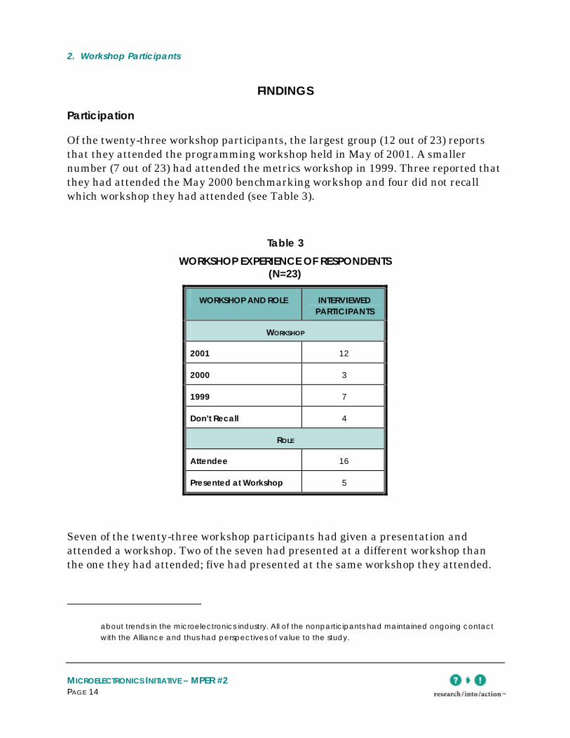
Participation
Of the twenty-three workshop participants, the largest group (12 out of 23) reports that they attended the programming workshop held in May of 2001. A smaller number (7 out of 23) had attended the metrics workshop in 1999. Three reported that they had attended the May 2000 benchmarking workshop and four did not recall which workshop they had attended (see Table 3).
Table 3
WORKSHOP EXPERIENCE OF RESPONDENTS (N=23)
WORKSHOP AND ROLE INTERVIEWED PARTICIPANTS
WORKSHOP
2001 12
2000 3
1999 7
Don’t Recall 4
ROLE
Attendee 16
Presented at Workshop 5
Seven of the twenty-three workshop participants had given a presentation and attended a workshop. Two of the seven had presented at a different workshop than the one they had attended; five had presented at the same workshop they attended.
about trends in the microelectronics industry. All of the nonparticipants had maintained ongoing contact with the Alliance and thus had perspectives of value to the study.

2. Workshop Participants
MICROELECTRONICS INITIATIVE – MPER #2 Page 15
Professionals from semiconductor manufacturers were the largest group in attendance: just under two-thirds (15 out of 23) of the workshop participants were employed at a semiconductor manufacturer. A third of the participants (7 out of 23) were from engineering design firms, and one workshop participant was from a polysilicon manufacturer.
Value and Influence of Workshops
The majority of the professionals with whom we spoke say that the Alliance has had a positive influence on the amount of attention paid to energy efficiency in the microelectronics industry. Over three-quarters (22 out of 26) of the respondents say that the Alliance has had a positive influence on efficiency. Seventeen respondents were able to articulate the reasons they believe the Alliance has had an influence in their industry.
The top two reasons given for the Alliance’s success in influencing the attention paid to energy use are: (1) the communication, collaboration, and networking fostered by Alliance activities; and (2) the effective selection of projects and funding support provided by the Alliance. Eleven out of seventeen respondents gave one or both of these reasons. Three remarked that, while some credit for the change in attention paid to energy use is due to the Alliance, the energy crisis of 2001 and escalating electricity prices have also driven companies to increase their focus on energy efficiency.
Nearly all (22 out of 23) of the workshop participants say that they discussed energy efficiency ideas and solutions from the Alliance workshops with others at their firms. Of the twenty-two who had discussed ideas, two-thirds (15 out of 22) say that their suggestions had been implemented or taken into serious consideration.
We asked the respondents to describe their experiences in implementing the ideas they had taken from the workshop. The responses were, in most cases, non-specific (perhaps to protect proprietary information) and, with one exception, unique to each individual. Tables 4 and 5 summarize the actions participants reported taking as a result of their experience at the workshops. Table 4 identifies efficiency actions taken by participants and Table 5 identifies efficiency suggestions made by participants that are under consideration or were rejected by management.

2. Workshop Participants
MICROELECTRONICS INITIATIVE – MPER #2 PAGE 16
Table 4
INFLUENCE OF WORKSHOP ON PARTICIPANTS INTERVIEWED
ACTIONS TAKEN AFTER WORKSHOP
Reduced cleanroom airflows and verified that reduced airflows had no impact on air quality. We are saving $100,000 a year in energy bills
Purchased more fan-powered filters and confirmed the energy efficiency of the fan-powered filters
Lowered fan sped and air filter face velocity
Reduced energy consumption through heat recovery from chillers
Changed internal methods to increase energy efficiency
Specifying more energy-efficient equipment and lighting
Improved monitoring. Installed sensors
Writing software code for monitoring that takes advantage of energy efficiency ideas discussed at the workshops
Looked at efficiencies in lighting, motors, chilled water, pumping, cooling towers
Table 5
INFLUENCE OF WORKSHOP ON PARTICIPANTS INTERVIEWED, CONTINUED
ACTIONS SUGGESTED AFTER WORKSHOP
Confirmed that energy-saving ideas will not have an impact on production; working on convincing production management to implement some measures
Presented the idea of working with the Alliance on a project in 2001—unable to sell the idea because the data [we were working with] was viewed as sensitive
Presented ideas for reducing energy used by cleanrooms; management considered it seriously but rejected it because the timing was not good
Created momentum within the company to examine exhaust systems and process to reduce energy. Momentum has diminished recently
Suggested closer monitoring of energy at the facility
Made suggestions during cleanroom remodel that would save 60% of typical energy

2. Workshop Participants
MICROELECTRONICS INITIATIVE – MPER #2 Page 17
consumption; client rejected the suggestions
Most participants report positive benefits for their work efforts as a result of workshop attendance. Table 6 shows that three-quarters say that attending the workshop provided them with new ideas or ways of thinking about energy. Nearly three-quarters (70%) say that the information presented in the workshop increased their awareness of the importance or benefits of energy efficiency. Several of those who said that the workshop did not provide new ideas, or increase awareness or interest, also made remarks such as “I was already aware,” or “although the workshop didn’t give me any new ideas, it did reinforce my thinking about the ideas.”
Table 6
WORKSHOP INFLUENCE ON PARTICIPANTS (N=23)
ATTENDING WORKSHOP … NUMBER PERCENT
Provided New Ideas or Ways of Thinking about Energy
17 74%
Increased Awareness of Importance or Benefits of Energy Efficiency
16 70%
Increased Interest in or Enthusiasm for Energy Efficiency
15 65%
Addressed Concerns about Moving to Energy Efficiency
11 48%
Half of the participants say that the workshop addressed some of the concerns they had about moving to greater energy efficiency. Nearly all of those who said that the workshop did not address their concerns explained that they did not have any worries about moving to greater energy efficiency before attending the workshop.
Nine out of ten participants say they would recommend the workshop to others and encourage the Alliance to hold more workshops (see Table 7). Three participants who said they would recommend the workshop qualified their remarks, saying “I’d recommend the workshop to select colleagues, depending on their experience.”

2. Workshop Participants
MICROELECTRONICS INITIATIVE – MPER #2 PAGE 18
Table 7
RESPONDENTS WHO WOULD RECOMMEND, ENCOURAGE ALLIANCE TO HOLD MORE, OR ATTEND FUTURE WORKSHOPS
(N=23)
PARTICIPANT WOULD: NUMBER PERCENT
Recommend Workshop to Others 22 96%
Encourage Alliance to Hold More Workshops 21 91%
Attend Future Workshop 19 79%
Nearly three-quarters (16 out of 23) of the participants say that they would like to see the Alliance hold an annual workshop.
Over two-thirds of the respondents (17 out of 23) praised the workshops for providing a forum in which they could form relationships with colleagues to discuss and share ideas. Several mentioned that they liked “the interactions” and “opportunities for networking.” In a similar vein, participants also mentioned that they valued hearing about “specific examples with data” and sharing information on metrics and benchmarking in the industry.
The only criticism of the workshop concerned what four participants perceived as a “commercial” tone to some of the presentations. Two of the four specifically mentioned that they wondered whether the analyses in the vendor presentations were biased. Another respondent mentioned that he felt he was listening to a “sales spiel” about the capabilities of the engineering firm, rather than a presentation on an energy-efficient solution. Three respondents mentioned that the presentations were “too vague,” or there was “not enough technical information or data” presented.
When asked what subjects they would like future workshops to address, respondents most frequently mentioned wanting specific examples of new developments or research in energy efficiency for the microelectronics industry. Table 8 shows that over one-third (8 out of 23) of the participants requested that future workshops include findings from new research. Nearly half (11 out of 23) of the participants also requested that future workshops cover energy efficiency improvements in either air handling or chiller systems. “Selling” energy efficiency to managers or clients was also named by nearly a quarter of the participants as an important management tool about which they would like to learn more.

2. Workshop Participants
MICROELECTRONICS INITIATIVE – MPER #2 Page 19
Table 8
DESIRED WORKSHOP TOPICS (N=23)
TOPIC NUMBER
NEW DEVELOPMENTS, RESEARCH
Cutting-Edge Ideas, New Designs, Updates on Research, More Specific Topics
8
New Energy Code 1
BUILDING SYSTEMS
Air Handling, Exhaust Systems, Compressed Air 6
Chillers, Cooling Towers, Variable Speed Pumping, Evaporative Cooling
5
Efficiency of Central Plants, Energy Centers 3
Chilled Water, Heating Water, Boilers 3
Energy Reduction in Process Equipment 2
Motors 1
Heat Recovery in Exhaust Stacks, Hot Water Applications 1
MANAGEMENT, PROJECT ANALYSIS
“Selling” Energy Efficiency Within Own Company or to Clients 5
Other Company’s Processes, Systems, Case Studies 2
Short Payback Horizon for Equipment 2
Benchmarking 2
Obtaining Project Funding (from the Alliance, Other Sources) 2
LEED Guidelines 1
Awareness of the Energy Crisis 1
Process Control Improvement 1
POWER GENERATION
Utility Pricing 1

2. Workshop Participants
MICROELECTRONICS INITIATIVE – MPER #2 PAGE 20
Distributed Generation 1
PV Panels, Renewables 1
Design Guidelines
As shown in Table 9, nearly two-thirds (19 out of 30) of the participants say they are aware of the Design Guidelines for Cleanrooms from the Lawrence Berkeley National Laboratories (LBNL). About half (10 out of 19) are involved in some aspect of cleanroom design covered by the guidelines. Of those involved, three say they have used the guidelines; five noted that there have not been very many, if any, opportunities to design a cleanroom during the recent industry downturn. Participants who have not used the LBNL design guidelines say their firms had their own design specifications.
Table 9
PARTICIPANTS’ AWARENESS AND USE OF LBNL DESIGN GUIDELINES FOR CLEANROOMS
STATUS NUMBER PERCENT
Aware of Guidelines 19 63% (n=30)
Involved in Aspect of Cleanroom Design Covered by Guidelines
10 53% (n=19)
Have Used Guidelines 3 30% (n=10)
The three participants who had used the guidelines made remarks such as “I use some aspects of the guidelines, but not all of them.” One designer said, “Whether I use the guidelines depends on the client. Some know exactly the airflow rate, etc. They want ‘another one like the last one.’ The guidelines don’t work for those who know exactly what they want.” Another noted that it is “difficult to make a document that is ‘one size fits all.’”

2. Workshop Participants
MICROELECTRONICS INITIATIVE – MPER #2 Page 21
Alliance Influence on Industry
Respondents believe that the Alliance message has had significant market penetration in the semiconductor segment of the microelectronics industry (Table 10). Just under two-thirds (19 out of 30) of the respondents believe that the Alliance has reached between 50% and 100% of this segment with the message of energy efficiency. Roughly one-third of respondents believe that the Alliance has reached about half of the process equipment manufacturers in the Pacific Northwest, and one-third believe that half to three-quarters of design consultants are aware of the Alliance’s activities. Respondents were least sure of the Alliance’s market penetration with product manufacturers; over one-half (17 out of 30) of the respondents said that they did not know the extent to which the Alliance’s message has reached product manufacturers.
Table 10
ESTIMATES OF MARKET PENETRATION OF ENERGY EFFICIENCY MESSAGE (N=30)
MARKET SEGMENT ESTIMATED PROPORTION OF
MARKET REACHED BY ALLIANCE*
SEMICONDUCTOR PROCESS EQUIPMENT
MANUFACTURER DESIGN PRODUCT
MANUFACTURER
0% 0 (0%) 3 (10%) 0 (0%) 0 (0%)
1% to 49% 3 (10%) 11 (37%) 5 (17%) 0 (0%)
50% to 74% 7 (23%) 1 (3%) 6 (20%) 7 (23%)
75% to 99% 6 (20%) 2 (7%) 0 (0%) 2 (7%)
100% 6 (20%) 0 (0%) 0 (0%) 0 (0%)
Don’t Know/ Unsure 8 (27%) 13 (43%) 15 (50%) 17 (57%)
* Categories created from open-ended responses.

2. Workshop Participants
MICROELECTRONICS INITIATIVE – MPER #2 PAGE 22
SUMMARY
The Alliance workshops have been well received by the microelectronics industry in the Pacific Northwest. There is both evidence that facility staff have implemented ideas they learned about in the workshops and evidence that the workshops are influencing how facility staff think about energy in semiconductor fabs in the region.
The past participants made suggestions for topics for future workshops and overwhelmingly call for the Alliance to continue conducting workshops in the future.

MICROELECTRONICS INITIATIVE – MPER #2 PAGE 23
3. SPECIAL PROJECTS
DESCRIPTION OF THE SPECIAL PROJECTS
As part of the venture, the Alliance funded special projects with three chip manufacturers: Hewlett-Packard, Intel, and Zilog. As part of this work, all three projects paid for energy-efficiency consulting engineering firms to analyze the energy used in the chilled water plants serving the manufacturing process. The consultants identified actions that would save energy and identified the costs of these actions, including capital, labor, and any other costs or impacts. The special projects could reduce energy consumed by the plant according to the extent that the recommended actions were undertaken.
To prepare this assessment of the Alliance special projects, we interviewed the consultants and chipmaker facility engineers responsible for each project. A copy of the interview guide is provided in Appendix B.
Manufacturer – Hewlett-Packard / Consultant – EN-WISE5
Hewlett-Packard (H-P) decided to implement the Alliance special project at their main North American fabrication plant in Corvallis, Oregon. The project proposal, which focused on achieving energy efficiency in the plant’s chilled water systems, was attractive to decision-makers at the semiconductor manufacturer because it combined energy efficiency with improvements to their production process. In addition, the reputation of the Alliance, the funding the Alliance offered, and the reputation of the consultant were also influential in Hewlett-Packard’s decision to implement the project.
The engineering firm of Engineered Web Information Systems, Inc. (EN-WISE), led by Mr. Kris Kinney, conducted the analysis. A significant part of project resources were applied to upgrade H-P’s existing process monitoring and control (SCADA)
5 The description of the project was drawn from Reports #1 and 2, “Chiller Efficiency Study,” prepared by Engineered Web Information Systems, Inc. for Hewlett-Packard, Inc., Northwest Energy Efficiency Alliance, and Pacific Corp, June 8, 2001 (report #1) and August 31, 2000 (report #2).

3. Special Projects
MICROELECTRONICS INITIATIVE – MPER #2 PAGE 24
system. Prior to the project, the control system was used primarily for process control, to obtain real-time data for fault diagnosis, and for monthly departmental cost allocation.
EN-WISE upgraded the SCADA system by adding high-precision temperature and chilled water flow measurement capability, as well as additional electrical metering. The added capability will enable the metering of energy use and BTUs for the chilled water (CHW) and chilled glycol/water delivery systems. These in turn will support key chiller system performance metrics.
In addition to these upgrades, EN-WISE installed “Electric Eye” data visualization software (accessible through H-P’s Intranet). This software enables the routine tracking and assessment of system efficiencies. As a result of hardware and software modifications, H-P staff will be able to easily display efficiency trends for chiller system and subsystems (in kW/ton). The software will show metrics and support benchmarks that show current and potential operating efficiency.
The first report delivered to H-P provided early “conventional” audit-based recommendations for no- or low-cost improvements to the central plant chilled water facilities. The second report addressed findings and recommendations based on instrumented data and an airside audit.
The first report made five no-cost recommendations and the second report offered an additional three no-cost recommendations. These no-cost recommendations and their associated estimated energy savings are given in Table 11. H-P staff responsible for the project said during telephone interviews that H-P has implemented all no-cost recommendations.
The consultant estimated that these no-cost measures would generate annual electricity savings worth about $460,000. Such savings would exceed the total venture cost for the H-P project, including the costs to H-P, fees to the consulting firm, and Alliance incentives and administrative costs.
In addition to these measures, the reports offered numerous low-cost recommendations, such as actions that would require inexpensive upgrades or a technician’s labor for perhaps a few weeks. The reports also offered a few measures that require larger capital outlays with paybacks between a few months and a few years. For example, the consultant estimated that one measure requiring a $100,000 investment in equipment and renovations would generate savings of $600,000 in annual energy costs.

3 Special Projects
MICROELECTRONICS INITIATIVE – MPER #2 Page 25
Table 11
EN-WISE NO-COST RECOMMENDATIONS TO H-P*
RECOMMENDATION ESTIMATED ANNUAL SAVINGS
FROM FIRST REPORT
ECM #1 Sequence Most Efficient Chillers to Operate First Greater than 1,314 MWh
ECM #2 Vary Fab Chilled Water Setpoint Seasonally 180 MWh
ECM #3 Stage Chillers to Minimize Part-Load Operation 1,972 MWh
ECM #4 Reduce Electrical Heat User for Pipe Freeze Protection 54 MWh
ECM #5 Reduce Transformer Losses (example 1) 131 MWh
Total “No-Cost” Estimated Annual Savings from First Report 3,651 MWh
FROM SECOND REPORT
ECM #4 Reduce Compressed Air Pressure 4,036 MWh
ECM #5 Run Least Efficient Glycol Chiller Last in System 3,928 MWh
Total “No-Cost” Estimated Annual Savings from Second Report 7,964 MWh
TOTAL FROM BOTH REPORTS
Total “No-Cost” Estimated Annual Savings from Both Reports* 11,615 MWh $464,600
* Dollar savings estimated at $40 per MWh. The estimated savings are drawn from the consultant’s report and were not verified for this MPER.
The non-energy benefits of successfully implementing these projects could include:
Ø Less mechanical wear on production tools;
Ø More finely-tuned control of peak load demand;
Ø New production tools to visualize equipment performance and trends that will optimize the production process; and

3. Special Projects
MICROELECTRONICS INITIATIVE – MPER #2 PAGE 26
Ø More sophisticated staging and sequencing of equipment.
H-P has expressed interest in expanding the project to its other facilities as funds become available.
Manufacturer – Intel / Consultant – Willis Energy Services
Opti-Chill is a proprietary process approach to efficiency for large chilled water systems developed by Willis Energy Services. It provides a step-by-step methodology for monitoring, measuring, modeling, and validating equipment operations in a chilled water plant. Intel became interested in working with the Opti-Chill approach for several reasons. Primarily, stakeholders were interested in achieving greater energy efficiency with cooling equipment. Furthermore, participation in the Opti-Chill project enabled Intel to demonstrate to the public that the company was actively pursuing energy efficiency. In addition, the threat of higher energy prices at the project’s inception in 2000 was a contributing factor in the decision to participate. The sophisticated instrumentation installed through the project to measure equipment energy usage also provides more data for non-energy production process control, which benefited engineering staff responsible for the fabs.
The project was fully implemented at Intel’s Fab 15 and Fab 20 in Hillsboro, Oregon, where consultant Paul Willis of Willis Energy Services, Ltd. performed the efficiency analysis of Intel’s chilled water systems using Opti-Chill. Initially, Intel engineers identified three fabrication plants that might qualify for the Opti-Chill project. Equipment modeling at the first plant, Intel’s Fab 15 in Aloha, Oregon, started in the second quarter of 2000. Two plants required the purchase of additional instrumentation to gather the necessary data. As of August 2002, engineers planned to measure and monitor equipment performance in order to investigate which recommendations might be implemented.
Willis combined critical plant data such as the cooling load profile, system configuration and sequencing, and local weather conditions into the Opti-Sim™ model that simulates chiller operations. To validate the performance of the equipment, Willis compared baseline performance metrics of the plant’s chillers, towers, and pumps against the manufacturers’ performance benchmarks. Results from the modeling and equipment performance data pointed to key variables that could be controlled to produce greater equipment efficiency.
Willis identified that controlling the cooling loads, equipment configuration, and operating protocols would be the most feasible efficiency measures for Intel engineers

3 Special Projects
MICROELECTRONICS INITIATIVE – MPER #2 Page 27
to implement. A cost-benefit analysis of several efficiency recommendations for the chiller equipment outlined the potential annual energy savings, the number of payback years, and the cumulative energy payback for each measure. This analysis provided a basis for decision-making regarding the recommended efficiency measures.
Willis created an “Opportunity Identification Report” for each fab. Table 12 gives the recommendations Intel has implemented, according to staff responsible for the project. The paybacks associated with these measures range from about five months to about nineteen months.
Table 12
WILLIS RECOMMENDATIONS IMPLEMENTED BY INTEL
RECOMMENDATION ESTIMATED ANNUAL SAVINGS
RECOMMENDATIONS FOR FAB 15
Replace Tower Spray Nozzles 111 MWh
Chiller & Tower Staging and Change Setpoint to 70° F 1 1,966 MWh
Reduce and Rebalance Condenser Water Flow 137 MWh
Trim Condenser Water Pump Impellers 296 MWh
Total Estimated Annual Energy Savings for Fab 15 2,510 MWh
RECOMMENDATIONS FOR FAB 20
Change Condenser Water Setpoint to 70° F 2,350 MWh
RECOMMENDATIONS FOR BOTH FABS
Total Estimated Annual Savings for Both Fabs2 4,860 MWh $194,400
1 Although this measure appears to be two measures, the estimated savings were calculated for both measures performed concurrently.
2 Dollar savings estimated at $40 per MWh.
3. Special Projects
MICROELECTRONICS INITIATIVE – MPER #2 PAGE 28
To elaborate, the measures involved the following:
Ø Replace Tower Nozzles—Change the cooling tower spray nozzles to maintain minimum flow and produce a more uniform temperature
Ø Chiller & Cooling Tower Staging—Change automatic sequencing of chillers and cooling fans
Ø Change Condenser Setpoint to 70° F— Add plates on the heat exchanger to allow for cooler water temperatures from the condenser
Ø Reduce Condenser Flow and Balancing—Reduce and rebalance condenser water flows to initial design conditions
Ø Trim Pump Impellers—Reduce the diameter of condenser pump impellers to optimize performance
Willis recalls that, after a few months of operation, the engineers at Fab 15 found that they had reduced their chiller energy use by 15% “or enough to supply about 200 homes.” Monitoring instrumentation confirmed the energy savings. One Intel engineer recalls the dollar value of the savings as “between $90,000 and $100,000 a year.” Regarding the decision-making about measures that did not prove feasible, the engineer said the company evaluated the measures according to how implementation might affect their facility, cost to implement, and the potential savings in kilowatt-hours. Two of the rejected measures were deemed to pose too great a risk to production to be implemented, and a third recommendation had a return on investment horizon that was longer than acceptable. Of this third measure, the engineer explained, “We had to draw a line about the measures. The sixteen-year payback to repipe the condenser system header was outside the realm of feasibility.”
Manufacturer – Zilog/ Consultant – Supersymmetry
Chip manufacturer Zilog chose to undertake the Alliance special project after stakeholders attended an Alliance-sponsored workshop on increasing energy efficiency in the microelectronics industry. The decision-makers at Zilog realized that there were opportunities to save energy in their operations. The incentives the Alliance offered for Zilog to conduct the study convinced the company to participate. In addition, Zilog staff realized the competitive benefits of achieving greater energy efficiency in equipment operations. At the time the study was undertaken, the firm was just beginning to recognize that its financial position was shaky. The project was implemented at Zilog’s facilities located in Nampa, Idaho.

3 Special Projects
MICROELECTRONICS INITIATIVE – MPER #2 Page 29
Supersymmetry, Inc. (now Rumsey Engineering), headed by Peter Rumsey, provided the analysis for Zilog’s chiller equipment. Rumsey installed instrumentation to monitor energy usage on Zilog’s cooling system equipment (motors, chillers, pumps, towers, and air handlers) and to establish energy-use benchmarks.
The data provided by the instrumentation justified the next step: implementation of some of the recommended measures. Zilog’s criteria for feasible projects included measures with a return on investment horizon of two years or less, and projects for which the return outweighed the risks and labor investment.
The project coordinator at Zilog sought the opinions of the maintenance supervisor and electrician to assess the risks and long-term maintainability of the measures.
Shortly after Zilog participated in the Alliance project, the company filed for Chapter 11 bankruptcy. The Zilog engineer said that the company immediately implemented the no-cost recommendations but was unable to implement any others. The engineer was satisfied, however, with the quality of the project and the recommendations offered. As the plant for which the study was done is not currently producing chips, we do not include a description of the implemented measures and their estimated energy savings.
PROCESS ISSUES
In 2000, the projects were designed with a division of responsibility between the consultants and the chipmaker staff. The consultants were responsible for the bulk of the work and equipment necessary for the ventures and the chipmakers agreed to provide in-kind contributions of relatively small amounts of labor and various materials.
For all three special projects, the major stumbling blocks to implementation in 2000 were project management issues. Consultants and chipmakers mentioned communication and the clarification of roles as specific problems. Two years later, both groups report a smoother process.
Between 2000 and 2002, the project manager for the Alliance changed. In part as a consequence of this transition, the consultants saw an improvement in communication with the client, and therefore an improvement in the project implementation. One consultant reported, “The new project manager’s approach was flexible. Initially, he had a more ‘hands-off’ approach, which was appropriate, and when the time came, he stepped in and helped me.” He continued, “I felt his approach

3. Special Projects
MICROELECTRONICS INITIATIVE – MPER #2 PAGE 30
was very responsive to conditions in the field.” Another consultant said, “I have been very satisfied with the Alliance’s role in this project.”
In 2000, the biggest challenge for meeting schedule deadlines arose from database problems at Hewlett-Packard. Mid-way through the project, H-P made changes to its operations database, rendering outputs that were incompatible with the modeling software as it had been originally configured. The negotiations around reconfiguring the modeling software resulted in a schedule delay of five months. This problem was resolved and the consultant recommended a stronger integration of information technology (IT) staff into the initial project planning for any similar projects in the future. He added, “We need to look at all the players when planning a project like this.”
During the project startup, the manufacturers’ requirements for confidentiality and nondisclosure limited implementation. One consultant found he could only employ subcontractors approved by the microelectronics firm to work on their site. The project construction was completed, but the costs exceeded his initial estimate.
The consultants for both companies say they have seen a change in staff attitude towards energy use since the inception of the special projects. “The projects have demonstrated that the microelectronics firms can understand and improve their energy systems. That’s a positive change.” Resources for implementing further change, however, have not been made available. Observes a consultant, “I see a high level of commitment to energy efficiency within the microchip manufacturing company, but any new project development efforts will still need staffing and money.”
Staff at both microelectronics firms expressed satisfaction with the job that the consultants had done. An engineer at one plant spoke for others in saying, “I would hire that consultant again for another project.”
BARRIERS
The boom market of the late 1990s and subsequent downturn in 2000 have intensified the competition among microelectronics firms, weeding out all but the largest and most profitable chipmakers. One consultant summed up companies’ reactions to the roller coaster market conditions: “Either a company is cash-strapped; therefore unwilling to spend money on anything that doesn’t have an immediate return on investment, or it is busy trying to squeeze the last drop of production out of a facility during a boom period.”

3 Special Projects
MICROELECTRONICS INITIATIVE – MPER #2 Page 31
As a consequence of the market conditions, the organizational culture of microelectronics firms, according to both firm staff and consultants, is characterized by risk aversion. The corporate emphasis on creating the greatest profit with the least risk and the lowest investment possible pervades all levels of decision-making. Because energy costs represent a small proportion of the total production expenditures and implementing efficiency measures may pose a risk to production, saving energy is a lower priority than boosting production output.
Simple and complex measures alike must be proven through modeling or experience. One consultant relates that, “The political pressure within a company hierarchy is to stay away from risky ideas, to avoid championing new concepts that haven’t already been endorsed by a superior.”
The losses associated with production failures are so great that managers and staff may lose their jobs when production halts. One consultant added, “No one in the company judges a plant manager’s work based on the energy savings he obtains. He’s only judged on output.” Another consultant illustrated the problem, saying, “An energy-efficiency retrofit takes time and the plant can run without it.”
Consultants for all three manufacturers mentioned the dearth of technical staff time at the manufacturer as a barrier they faced. As staffing levels have dwindled, consultants have found that engineers are hard-pressed to find time to think about a project, much less perform the studies or experimentation necessary to justify the measure. One consultant remarked, “It’s hard for us to get the plant engineers’ time and attention. They are busy putting out fires.” Another noted that the type of special projects that the Alliance has funded require the decision-making authority of the executive staff, and the technical expertise and time of engineers. He continued, “You can’t sell a project like this just to the president. You need to also sell it to technical staff but it’s hard to get their attention.”
An example follows of an efficiency opportunity that will not be achieved due to the barriers of both staff time risk aversion. “One manufacturer has specifications for filters that are ten years old. Consultants estimated that replacing some of the filters could save $90,000 a year but the ten-year-old specs are still in place. New specs would need to be written—a task no one has time for—in order for the more efficient filters to be purchased.”
Exacerbating these barriers, engineers at the microchip manufacturers tend to believe that they already know how to achieve energy efficiency in their operations and that they are doing all that can be done. This tendency to believe in their own

3. Special Projects
MICROELECTRONICS INITIATIVE – MPER #2 PAGE 32
expertise over the knowledge and reputation of their consultants creates a dynamic in which the consultant must “prove himself two or three times over.”
The intense competition limits the potential for energy savings from Alliance-funded projects in another way than time and risk constraints. Only the least-sensitive areas of operations were considered for these special demonstration projects. Observes one consultant: “The fear of divulging proprietary information holds back manufacturers from participating in Alliance projects.”

MICROELECTRONICS INITIATIVE – MPER #2 PAGE 33
4. H-P DESIGN CHARETTE
INTRODUCTION
This chapter discusses the H-P Design Charette and presents an assessment of the influence of the Charette on the design of the H-P Fab renovation.
Description of Project
The Hewlett-Packard (H-P) Design Charette was conducted in February 2002. The charette is a direct outgrowth of H-Ps experience with the Special Project Fund and the workshops sponsored by the Alliance.
In December 2001, the facility energy manager was notified that a corporate decision had been made to renovate one of the semiconductor fabrication facilities at their Corvallis campus. The project was nearing final plan, having already been through several iterations between the corporate office and the design firm; the facility energy manager was then asked to see what he could do to for the project at the local level.
The local facility energy manager was also aware that the State of Oregon had passed legislation, due to go into effect March 2002, that would permit H-P to self-direct public benefits funds for efficiency projects at their own site. Given H-P’s experience with the Alliance workshops and a special project on their chilled water system, the energy manager contacted the Alliance to discuss what opportunities might exist given the plans for the renovation.
There was a narrow window of opportunity to come up with energy efficient solutions for the design: the ideas needed to be developed before the design was finalized in March 2002. The Alliance suggested that a design charette6 would be a way to provide more information to the design process and agreed to fund the participation in the charette by some experienced semiconductor fabrication facility designers. H-P
6 A design charette is an intensive workshop where a project is subjected to an “out of the box” brainstorming session. A charette is also the first step in any integrated design process and has been used in design for all types of buildings and facilities to ensure that innovative efficiency options are considered in the design process.

4. H-P Design Charette
MICROELECTRONICS INITIATIVE – MPER #2 PAGE 34
was enthusiastic and the design charette was scheduled as soon as all parties could attend, in February 2002.
Study Approach
The evaluation activities for the H-P Design Charette occurred in two phases. The first phase involved attendance at the charette; the second phase involved interviews with key participants in the charette and subsequent design and construction activities. Participants included the Alliance project manager, the three consultants who participated in the charette for the Alliance, the project manager for the designer—Industrial Design & Construction (IDC)—and the two project managers for H-P. A copy of the interview guide is provided in Appendix C.
THE CHARETTE
A design charette for Hewlett-Packard (H-P) fabs was held on February 12 and 13, 2002, in Corvallis, Oregon. Eleven staff from H-P and its design firm, IDC, attended. Also in attendance were Bill Tschudi of LBNL, Michael Ponder and Jeff Harris of the Alliance, Peter Rumsey of Rumsey Engineers, and Tom Hansz of Facility Planning and Resources.
The afternoon before the charette, the three consultants took a tour of the building being renovated. The charette began the morning of the 12th with an overview of the project and a presentation by Tschudi about cleanroom benchmarking.7
The charette began with a discussion of some of the constraints faced by the team designing the H-P facilities. Mid-morning, H-P staff noted that they had done a lot of review and that they were ready to hear new ideas and to engage in a discussion to generate new approaches. Mid-afternoon, after the generation of ideas, the concepts were winnowed and prioritized.
At the outset of the charette, H-P and IDC noted that the schematic design for the project was already in process, so there was no possibility to consider major changes. However, there was some room for new ideas to modify or improve what was still under plan.
7 An LBNL website (http://ateam.lbl.gov/cleanroom/) provides information on how energy is allocated for different types of cleanrooms.

4. H-P Design Charette
MICROELECTRONICS INITIATIVE – MPER #2 Page 35
Constraints to Energy Efficient Design
Existing systems constitute the primary constraint to new ideas. H-P indicated that they were not interested in retrofitting existing systems. They said they would look at new ideas for new fabs. The most they would be willing to do to existing systems was to “tweak” them.
Another constraint is that the building systems for a fab need to be “infinitely” flexible. This limits the opportunity for some types of solutions, while providing an opening to others.
As expected, the process team constrains the system. They do not want to have any changes to their manufacturing process. The process for manufacturing semiconductors requires a closely controlled environment, and because this H-P facility is used for research and development, the process environment has to be particularly constant.
Previous bad experience also constrains what can be done. When an idea “sounds like” something that did not work in the past, there is hesitancy to even test it again. This hesitancy persists, even though an expert such as those offered by the Alliance may suggest it can work, or even though the designer has been successful designing similar systems for others. H-P indicated it was not willing to explore such ideas.
Available incentives can constrain designs by pointing the designers in a particular direction. For instance, if incentives for fuel switching are available, H-P will look at opportunities to shift their electric use to gas. If the only incentives are for electricity efficiency, they will only look at electric-based approaches. To use free cooling as an example: it needs some preheating (new gas capacity), but this results mostly in a reduction in electricity usage; without some incentive for new gas capacity, the idea of free cooling cannot be considered.
Lack of data is often a constraint. Even when data are available, the concern is either that they may not pertain to the specific site or that it is difficult to interpret what they mean for that location. There is always uncertainty regarding how applicable to specific project conditions are data results from another application.
One must estimate baseline and alternative conditions, which can be difficult. This is a barrier for systems that customize components such as fan filter units and fan conditioning blocks. This is also an issue for all of the system options where the different configurations must first be designed before effects can be estimated. This process increases the cost of the project considerably. Someone in the charette noted

4. H-P Design Charette
MICROELECTRONICS INITIATIVE – MPER #2 PAGE 36
that a simple switch from T-12 to T-8 fluorescent lamps might be the only technology for which energy savings can be easily calculated.
Results from the Idea Generation
Forty-five ideas were generated by noon of the 13th. The ideas were then winnowed, prioritized and assigned to different teams for follow-up. From this:
Ø One idea was added during the discussion;
Ø Nine ideas were eliminated either because they duplicated other ideas or were not worth further consideration;
Ø Twenty-three ideas were assigned to IDC to review and conduct a net present value (NPV) analysis (these were assigned to category A);
Ø Three ideas were assigned to the Alliance to develop (category B);
Ø Seven ideas were assigned to the Alliance to be considered as something to do at some time in the future, but were outside the scope of the H-P project (category D); and
Ø Four ideas were deemed to be “best practices” that “IDC should do, period” (category E).
At the close of the meeting, all agreed that all items in Category E would be included in the plan. It was decided the Alliance and IDC would develop their analyses of categories A and B by February 21, 2002, as well as any ideas in category D that needed to have an aspect considered for the new project. Finally, H-P would then take the analyses and decide whether to include or not include an idea in the final schematics by February 22, 2002.
FOLLOW-UP INTERVIEWS
There are five key questions that we sought to address in the follow-up interviews:
1. Did the design charette influence the design and construction of the fab renovation?
2. If the design charette did have some influence, what are the resulting estimated savings?

4. H-P Design Charette
MICROELECTRONICS INITIATIVE – MPER #2 Page 37
3. Is the charette likely to have any long-term influence on H-P, either at the Corvallis facility or other facilities worldwide?
4. Did the charette have any influence on the design firm, IDC?
5. Do design charettes provide a useful market transformation tool for the Alliance?
The answers to the first, second, and third questions are unequivocally yes; and savings can be estimated based on work done by Rumsey Engineers. The answer to the fourth is more difficult to discern, and the answer to the fifth is yes, with some caveats.
Overall Impressions of the Charette
H-P and the Alliance had different but overlapping goals in conducting the charette. H-P was looking for more specifics, beyond the generic material presented in the Alliance workshops: something that would spark their imagination and get some new energy efficiency solutions into their building. The Alliance was hoping to ensure that H-P included as much energy efficiency as possible in their renovation and the Alliance wanted to initiate a dialog with IDC, the designer for the project.
The Alliance proposed the charette as a means of accomplishing all of these goals and H-P agreed. Initially, IDC was concerned that the charette would interfere with the schedule for the project. The project manager was also doubtful that new ideas would surface that had not already been considered and discarded as being outside the project’s scope.
The charette was conceived and implemented in a very short time. The consultants on contract to the Alliance consider this type of fast track schedule “normal” for the design of semiconductor facilities, and they were able to make the time to attend. All three of the consultants participate in charette-type events several times a year.
Two of the consultants (Rumsey and Tschudi) offered presentations on some of the benchmarking and performance results for projects they have studied. These presentations were similar to presentations they had made at Alliance microelectronics workshops; however, they were able to tailor their comments in the presentation to the specific building under review. This was well received by charette participants.
4. H-P Design Charette
MICROELECTRONICS INITIATIVE – MPER #2 PAGE 38
The third consultant acted as the facilitator. Curiously, two of the three consultants had been employees of IDC at some time in their career. Nonetheless, as noted above, IDC staff were somewhat uncertain about the value of the process. During the charette there appeared to be a slow thawing on the part of IDC, and by the second day there was a fair amount of enthusiasm from them.
The overall assessment of the charette from the three consultants’ points of view was that it generally went as well as others they had had. However, there were two significant weaknesses. One was the hesitancy of IDC to participate. All of the consultants thought that a telephone or face-to-face meeting prior to the charette could have assured IDC that H-P was committed to the process and the possible outcome. Reluctance on the part of an existing design team is a common feature of charettes that are held late in the planning process, as they are generally working on a tight time schedule and are resource-constrained. The potential for additional work is perceived first as a threat to the schedule and existing resources, only secondarily is it perceived as additional opportunity.
The other weakness noted by the consultants was the late point in the design process at which the charette was held. Normally, there are three steps in the process:
1. Schematic design
2. Design development
3. Final design and drawing
The charette occurred during the design development phase, and the consultants noted that it could have been more productive if it had occurred during schematic design. As a result of its charette experience, H-P now believes it would be beneficial to utilize this process earlier. The corporate project manager noted that for future projects, such as one currently in the planning stage, they will be using a design charette earlier in the planning.
All three consultants perceived H-P to be excited and committed to the charette. One noted that his perception of the number of project ideas seriously considered by H-P was much greater than often happens with charettes this late in the process. The enthusiasm for the charette was confirmed in interviews with H-P. The two project managers for H-P both felt that they got what they had hoped for: projects that would reduce energy costs for H-P and could qualify for funding from the self-directed funds pool. One of the project managers said:

4. H-P Design Charette
MICROELECTRONICS INITIATIVE – MPER #2 Page 39
“The Alliance seems to have access to industry experts that I wouldn’t have known. They brought things to the table with expertise. [They] looked at our project specifically, getting away from general ideas to the specific unique problems at H-P.”
H-P project managers also noted that the charette had not necessarily brought up things they had never considered, but the ideas were offered in context of the specific project and the presentations were clear, engineering based, and contained sound information. Another factor for H-P was that they consider themselves to be seriously interested in energy efficiency, so they were interested in seeing if there could be something new. The analysis done after the charette to flush out the ideas provided a great deal of information. H-P was able to use this both to decide whether to proceed with further analysis, as well as whether to initiate the application for the self-directed funds.
IDC’s project manager did not feel that the charette offered any new concepts that could be implemented. There was design constraint, in that they could not make any changes to the central plant, which limited the possibility of implementing many of the ideas. In the IDC project manager’s assessment, the concepts that were discussed were already under consideration and had been either rejected or accepted prior to the charette. He further noted that most of their clients want to be “as green as possible.” Thus these issues are constantly of interest to them.
Nonetheless, the IDC project manager also judged the discussion as useful and interesting, even though it did not, in his view, affect the project. All of the best practices identified in the charette (Category E) were included in the project. These include:
Ø Specifying energy efficient motors
Ø Specifying energy efficient lighting
Ø Specifying variable frequency drives (VFDs)
Ø Not oversizing mechanical equipment
Changes to Fab Design
After the charette concluded, Rumsey Engineers prepared a report on the category B and D measures assigned to the Alliance for review and development. This report (which is proprietary as it deals with process issues for H-P) documents savings

4. H-P Design Charette
MICROELECTRONICS INITIATIVE – MPER #2 PAGE 40
potential and possible financial benefits from using the Oregon Self-Directed Fund or the Oregon Business Energy Tax Credit.
To review what measures were installed, Research Into Action participated in a conference call between the two H-P project managers and Rumsey Engineers. The discussion during the call reviewed each measure in the report and assessed its status. The review identified whether the measure was being installed in the project (and if not, why); whether it was under consideration for the future; and whether, if installed, H-P had requested self-directed funds to help pay for the installation.
Table 13 presents the outcome for the project. Included are the measures examined by Rumsey Engineers for the Alliance, the estimated savings potential for each measure, and status of the measures after construction.
As the table shows, most of the operational measures and one of the recommended measures from the charette were implemented. Three of the recommended measures that were outside of the scope of the project are still under consideration for future implementation, with two already assigned to internal engineering staff for further investigation. The estimated savings are over 17,000,000 kWh even without estimates of savings for the operational measures.
During the discussion, which was held the day before the plant shutdown to begin switching over to the new equipment, several operational measures were noted by H-P as additional things they would do during the shutdown. They noted in particular that the discussion had jogged their memory about these operational measures. Thus, it appeared from the discussion that the timing was apropos and had increased chances that operational measures would be implemented.

4. H-P Design Charette
MICROELECTRONICS INITIATIVE – MPER #2 Page 41
Table 13
CHARETTE GENERATED MEASURES STATUS AFTER CONSTRUCTION
MEASURE EXAMINED ESTIMATED SAVINGS
STATUS APPLIED FOR SELF-DIRECTED FUNDS
OPERATIONAL MEASURES
Implement Dual Temperature Chilled Water Strategy
5 – high savings1 Implemented
Change Humidification Method to Evaporative Media
2 Insufficient gas capacity
Use Vfds2 On RO Membrane Pumps 1 – low savings Implemented Yes
Run Acid Exhaust Fans in Parallel 2 Implemented Yes
Specify Efficient Equipment 4 Implemented where possible
Yes
Install Low Loss Transformers 2 Implemented
INVESTMENT REQUIRED
Free cooling 2,000,000 kWh Might consider in the future
Occupancy Based Re-Circulation Airflow Setback
3,000,000 kWh Insufficient infra-structure in place for controls and communication
Use Run-Around Coils to Pre Cool and Reheat Make-Up Air
357,000 kWh / 57,700 therms
Not done ROI did not meet criteria
Velocity Reduction Savings Potential 606,000-2,860,000 kWh
Plan to do
Optimize Exhaust 1,400,000 kWh Examining for future
Add Sidewall Returns 395,000 kWh Not done poor effect on laminar
flow
Add VFDs To Cooling Towers 371,000 kWh Examining for future
Select Efficient Fan Filter Units 17,000,000 kWh Implemented Yes

4. H-P Design Charette
MICROELECTRONICS INITIATIVE – MPER #2 PAGE 42
1. A scale of 1-5 was used for the operational measures. A 5 means very high savings potential, while a 1 means worth consideration but with low savings potential.
2. VFD = Variable Frequency Drive
SUMMARY
The H-P design charette was quite successful in ensuring that energy efficiency measures and operational actions were incorporated into the design of a semiconductor fabrication renovation project. The savings are at minimum 17,000,000 kWh annually, and probably much greater, given the large number of operational measures installed and the VFDs specified that might not have been installed without the charette.
In addition, H-P is likely to pursue design charettes focused on energy efficiency for future design projects throughout the world. Finally, despite the skepticism expressed by the IDC project manager, IDC did contract with the Alliance to conduct a design charette for their 2002 energy efficient fab template. A future MPER will discuss the influences that led to that charette and whether there are broad impacts that can be traced back to the H-P process.
The consultants and H-P appear quite satisfied with the charette experience and the general outcome. While there are some suggestions for how to improve the organization of a charette, in general all agreed that this worked very well. The value of a charette as a market transformation tool seems to have been well demonstrated in this project.

MICROELECTRONICS INITIATIVE – MPER #2 PAGE 43
5. DENDRITIC POLYSILICON PRODUCTION
Advanced Silicon Manufacturing Inc. (ASiMI) is implementing the Dendritic Polysilicon Production project. The project is an outgrowth of the Shell Solar Silicon Crystal Growing Facilities project because of Shell’s need to find an additional source for specialized polysilicon material in order to expand their recharge process capacity. Dendritic polysilicon (or teardrop poly) is a pure silicon feedstock used for crystal growing that is much smaller than the chunk poly typically available.
In this chapter we discuss the study approach, the history of the teardrop polysilicon project, its current status and next steps for the evaluation.
STUDY APPROACH
The evaluation team is taking a process evaluation approach to this venture. We have attended quarterly meetings of the project, visited the ASiMI production facility in Moses Lake, Washington, conducted interviews with project participants, and visited users testing the teardrop poly: SEH America and Shell Solar. In addition, the project team reviewed the MPERs of the Shell Solar Crystal Growing Facilities project.8
PROJECT HISTORY
In this section, we discuss project initiation, the underlying market transformation theory, and the progress of the project in 2001 and 2002.
8 Reed, John H., Andrew D. Oh and Nicholas P. Hall (1999) Market Progress Evaluation Report 1: Silicon Crystal Growing Facilities E99-034; Peters, J.S. & S. Feldman. (2001) Market Progress Evaluation Report 2: Silicon Crystal Growing Facilities E01-090; Siemens Solar (2000) 1999 Annual Report, 00-050. Available at the Alliance website: www.nwalliance.org.

5. Dendritic Polysilicon Production
MICROELECTRONICS INITIATIVE – MPER #2 PAGE 44
Project Initiation
The Shell Solar Crystal Growing Facilities project was initiated in spring 2001. Its goal is to reduce energy requirements in the production of polysilicon feedstock for use by silicon crystal growers. The potential energy savings are 25% compared to the base product produced by the same process reactors.
The Alliance negotiated a contract with ASiMI to develop the teardrop polysilicon product. As part of the contract, ASiMI also arranged for Shell Solar and SEH America to conduct tests of the teardrop polysilicon product to determine whether it could be qualified as a feedstock material for their crystal growing processes.
To monitor the project the Alliance conducts a quarterly meeting with all contractual parties. The first meeting occurred in September 2001. Subsequent meetings have occurred on a regular basis, with updates from each participant as to their experience and findings relative to the teardrop product.
Market Transformation Theory
The market transformation premise for the project is grounded on the assumption that energy savings are available beyond the process of manufacturing teardrop polysilicon, and would come from the crystal growers who use the new product. The Shell Solar Silicon Crystal Growing project demonstrated significant energy savings, as well as production benefits from using smaller polysilicon feedstock in the crystal growing process. Currently only one provider, MEMC, produces a smaller feedstock. A teardrop polysilicon product from ASiMI could potentially be used by Shell Solar and by semiconductor silicon growing facilities. This would likely lead to energy savings in these production processes as well.
The market transformation theory at the core of this project, therefore, is the expectation that the semiconductor crystal growers in the Pacific Northwest will use the teardrop polysilicon product, and that this product will facilitate their increased use of recharge, leading to energy savings.
In the technical section at the close of this chapter, we discuss the differences between polycrystalline products and their use in recharging crystal growers.

5. Dendritic Polysilicon Production
MICROELECTRONICS INITIATIVE – MPER #2 Page 45
Project Progress
The first test batches of teardrop polysilicon material were shipped to Shell Solar and SEH America in fall 2001. At that time, the energy savings were confirmed in initial tests at ASiMI. At the same time, the semiconductor industry began to experience a significant economic downturn. In 2001, this was expected to last less than a year. In fall 2001, ASiMI ceased general production at their Moses Lake facility due to the economic downturn in the semiconductor industry, as there was limited demand for polysilicon. However, testing and crystal production using the teardrop material continued.
By January 2002, ASiMI had confirmed energy savings goals for the teardrop polysilicon material in the “A” reactors at the Moses Lake facility. Testing of the product at SEH and Shell were then able to begin, as SEH had internal approval to proceed and Shell had completed modifications to their recharge units.
In June 2002, the quarterly meeting provided updates on the status of the testing at SEH and Shell and revealed that ASiMI was going to move production of the teardrop product to their Butte facility. The test results at SEH and Shell had moved along well, although there were some technical issues SEH required ASiMI to address regarding product specifications. Shell, meanwhile, reported that the teardrop product was not working well in their available side recharge device. ASiMI agreed to work with both on their concerns.
The change in facility for production is the result of a joint venture between ASiMI and Renewable Energy Corporation to use the Moses Lake facility solely for polysilicon products for the photovoltaic industry. Moving production to the Butte facility will result in a different product than that produced by the Moses Lake facility, called “teardrop plus,” which will need to be requalified by SEH and Shell. This product will be produced in inherently more energy efficient reactors than was the original teardrop product, which could somewhat reduce the energy savings potential.
By September 2002, the project schedule had been revised by the move of production to Butte. ASiMI was able to report initial savings of 18% had been achieved with the “teardrop plus” product, and SEH and Shell indicated they had received shipments of the new product and were able to initiate qualifying studies. Uncertainty about production at the Moses Lake facility remained.
In December 2002, interviews with ASiMI staff confirmed that the Moses Lake facility was now operational and that a teardrop-type polysilicon product was being

5. Dendritic Polysilicon Production
MICROELECTRONICS INITIATIVE – MPER #2 PAGE 46
produced at the facility. An operational audit by the evaluation team is scheduled for early 2003 to determine whether the energy savings are still being obtained.
ASSESSMENT OF PROJECT PROGRESS
Impact of the Joint Venture and Production in Butte
The teardrop product that was made in Moses Lake is not the same as the one that will be made in Butte for a number of reasons – the foremost being that the new product will include crushed cores along with the dendrites.9 This product will be called “teardrop plus.” By producing teardrop at a new plant, all users will require new acceptance testing, similar to the testing of any new product.
The production of the Moses Lake facility will “belong” to Solar Grade Silicon, the Joint Venture (JV) between ASiMI and Renewable Energy Corporation. The intention of the JV is to produce polysilicon only for the photovoltaic or solar market. But the actual product flows may be more widespread. For example, there has always been a secondary stream from Butte for products that do not meet the quality criteria of the semiconductor market. Typically, this is sold to solar. The recipients of the secondary product stream for Butte may benefit Shell Solar, but this is unknown.
ASiMI is working on developing production of teardrop plus at their Butte facility and will then establish pricing. Pricing is usually more dependent on what buyers will pay than a function of production costs. At the end of 2002, all virgin polysilicon products were priced together near a ‘floor’ price, such that there is no cost advantage of teardrop. This is likely to change as market demand increases.
Other Market Issues
The demand for solar photovoltaic crystal wafers has been constant and even growing throughout the downturn that the semiconductor wafer market has been experiencing. The Moses Lake facility restarted in December 2002, and is focusing solely on producing a polysilicon product for the solar market. If the teardrop product is manufactured at the facility, there will be substantial energy savings.
9 When growing teardrop in the Butte reactors, the core is larger that from the reactors used in Moses Lake. The core is solid high quality polysilicon just like the dendrites, and it must be crushed and included with the dendrites for production to be cost-effective.

5. Dendritic Polysilicon Production
MICROELECTRONICS INITIATIVE – MPER #2 Page 47
Conditions in fall 2002 in the semiconductor wafer market indicated that product volumes are increasing slowly, but pricing remains depressed. As demand increases, production will increase and pricing will be affected. Teardrop and teardrop plus should be able to be priced competitively.
Locally, there is one very small manufacturer of side recharge equipment, Jax Industries. Jax developed the recharge system used by Shell Solar to work with the MEMC granular poly. Being small, Jax is unlikely to make a difference in either the solar or the semiconductor market. There are two major manufacturers of silicon growing furnaces: CGS and Kayex. Both manufacturers make a side recharge device for their furnaces that also work only with the MEMC granular products. Both also make center recharge devices that are likely capable of using a wider variety of poly products including teardrop.
One goal of the ASiMI project is to expand the product types that could be used in side recharge and thus open the market potential for side recharge. At this time neither teardrop nor teardrop plus can be used in the side recharge equipment utilized by Shell Solar, though development and testing is ongoing and Shell and ASiMI are hoping to address this.
At the same time, center recharge, which is more commonly used by semiconductor crystal growers, is less likely to produce the level of energy savings that can be produced with side recharge. Our conversations with semiconductor silicon crystal growers suggest that these firms are unlikely to shift to side recharge due to a variety of purity issues associated with it. (See the technical section below for more discussion of these issues.)
The result of these factors leads us to the current assessment of the project progress in achieving the expected goals:
Ø There are energy savings of at least 18% from production of teardrop plus compared to the more common chunk polysilicon (figures from Butte ASiMI), but the 25% savings previously achieved may not be achievable in Butte.
Ø The Butte and Moses Lake plants are the only plants worldwide that produce teardrop or teardrop plus.
Ø The Moses Lake plant can produce the teardrop product with 25% savings over chunk poly; and if it operates in 2003 at the same level as in 2000 and

5. Dendritic Polysilicon Production
MICROELECTRONICS INITIATIVE – MPER #2 PAGE 48
2001, a real energy savings for the plant will be achieved, but the product will only be available as solar grade polysilicon.
Ø There may be additional energy savings available from using teardrop in recharge for crystal growing. However, this is likely to come from the use of teardrop in the general crystal growing process, not in recharge.
Ø The energy savings appear to be significant only for side recharge—the more commonly used center recharge results in either no savings or lower savings.
Ø Silicon crystal growers like the teardrop product for use with chunk polysilicon as a way to more efficiently accomplish the initial charge; this could result in a small amount of energy savings, which would be of little consequence to the manufacturers.
Ø Side recharge has yet to be successfully demonstrated for teardrop or for teardrop plus products.
Ø There is interest in side recharge at this time only from one solar photovoltaic crystal grower—Shell Solar.
Ø There are no indications that side recharge will be applied to the broader semiconductor crystal growing market.
NEXT STEPS FOR THE EVALUATION
The next steps for the evaluation are focused on whether ASiMI production is resulting in energy savings at their Moses Lake and Butte facilities and whether energy savings are likely to accrue to semiconductor crystal growing facilities in the Pacific Northwest who use the teardrop plus product.
The activities that will be conducted in 2003 include:
Ø Continuing to track program progress;
Ø Conducting an operational audit of the Moses Lake facility and assessing energy savings and production levels;

5. Dendritic Polysilicon Production
MICROELECTRONICS INITIATIVE – MPER #2 Page 49
Ø Conducting interviews with semiconductor crystal growers to assess their interest in the teardrop plus product and the effect of teardrop plus on their approach to recharge;
Ø Conducting visits with Shell and SEH, and assessing the energy savings benefits of using teardrop plus in their facilities; and
Ø Providing documentation of the project in the next Microelectronics MPER.
TECHNICAL SECTION
Teardrop Polycrystalline Silicon
Teardrop polycrystalline silicon products (teardrop poly) are made using essentially the same process as chunk polysilicon with some changes to process variables. Teardrops are small dendrites, or branches formed on the outside of polysilicon rods. They are usually about one-inch long. Chunk poly is typically made from solid rods, broken into fist-sized or smaller pieces. (See Figures 2 and 3 below.)
Figure 2 Figure 3
TEARDROP POLY POLYCRYSTALLINE ROD & CHUNK POLY
An enlarged picture of teardrop (about one inch long) is on the left while a machined polycrystalline rod and chunk poly (about fist-sized) is pictured on the right.

5. Dendritic Polysilicon Production
MICROELECTRONICS INITIATIVE – MPER #2 PAGE 50
Teardrop can be used, and will continue to be used for both initial charge and for recharge in crystal growing (recharge is described below). It has some advantages in both situations, but is a nearly fully substitutable product for any other virgin chunk polycrystalline silicon. It is not fully substitutable, as in initial charges some mix of teardrop and chunk products seems to work best. The major benefits of teardrop or teardrop plus seems to come down to pricing. Teardrop is a product that uses less energy to make, and requires less handling or processing and therefore can be priced lower. Since teardrop is nearly fully substitutable for the chunk poly that wafer manufacturers already use, and because it will eventually meet acceptance testing as pure and reliable polycrystalline silicon, price remains the significant difference between teardrop and chunk poly.
There is another poly product, a granular one that is made in a completely different process, a fluidized bed. These granules are approximately bb-sized, and are made by one manufacturer, MEMC. This is the only product available worldwide for side recharge at this time. And since MEMC is a manufacturer of wafers themselves, when they are in full production there are limitations to how much granular poly product MEMC puts on the market. Thus, there is interest in an alternative to granular poly, such as teardrop, that can be made to flow in side recharge applications.
There are some other differences between teardrop plus and chunk poly: the sizing, the abrasive quality of teardrop, sharp edges of chunk, and potential for flow. But these appear to be relatively unimportant compared to price.10
Energy Benefits of Teardrop
Teardrop and teardrop plus (teardrop combined with the crushed cores) appear to use about 18% less energy per kilogram to manufacture than chunk poly (preliminary results from the ASiMI Butte plant). The fact that teardrop product uses less energy and requires less handling and processing means it can be priced lower.
For the semiconductor crystal growing market where center recharge is used, there does not appear to be an energy benefit from using teardrop poly. There may be some
10 Shell Solar MPER #2 reported that one of the problems with recharge using chunk is the damage to the crucible after two or three recharges. The chunk product is similar to broken glass and scratches the sides of the crucible.

5. Dendritic Polysilicon Production
MICROELECTRONICS INITIATIVE – MPER #2 Page 51
productivity benefits, but any energy benefits are small and apparently not important in this application.
For the solar photovoltaic wafer market, where there may be more potential for side recharge, there may be some energy and productivity benefits in the use of teardrop. But teardrop does not appear to be suitable for the side recharge equipment that is now available, and side recharge may apply only to the solar photovoltaic wafer market.
Description of Recharge Methods
There are two recharge methods in use – center and side. Center appears to be used for the semiconductor silicon crystal production and both center and side are used for the manufacture of solar crystal.
In center recharge, the pulled crystal is cooled and removed, and then the recharge batch is placed in the crystal chamber and manually poured into the crucible. Compared to the side recharge, center recharge does not have the same opportunity to maximize productivity by allowing the new charge to melt while the crystal is cooling. This saves about two hours, and for some crystal producers, this time is important. Center recharge also does not appear to have energy savings advantages compared to side recharge.11
The major savings from using recharge are not energy but productivity and consumables – by not cooling and reheating the quartz crucible its life is extended. The energy savings from recharge come from not having to reheat the crucible.
Center recharge is now used in semiconductor crystal growing by most Pacific Northwest crystal growers; side recharge is used only at Shell Solar. Side recharge equipment is apparently also available from the two crystal grower equipment manufacturers, CGS and Kayex. All side recharge equipment currently works only with the granular product made by MEMC. We have not identified any other firms in the region using side recharge. Side recharge may not be feasible for much of the semiconductor crystal market, as feedstock contamination and heat shield configuration may preclude its use.
11 Average savings from recharge increases with the number of crystal pulls, side recharge permits more pulls.

5. Dendritic Polysilicon Production
MICROELECTRONICS INITIATIVE – MPER #2 PAGE 52
There is no particular need to use teardrop for center recharge and, although it may have some small productivity benefits, there are no significant energy benefits. And even these productivity benefits may go away with the use of teardrop plus.
There is currently not yet any way to use teardrop for side recharge (only granular poly products work), and with advent of teardrop plus, which has a larger average size than does teardrop, it is unclear if it can be made to work.
No photographs or drawings of center recharge are available. However, Figures 4 and 5, below, show side recharge. Figure 4 indicates key components including: 1) the hopper, 2) flow control, and 3) the port where granular poly product is introduced into the crucible. Figure 4 is the CGS granular feeder; Figure 5 is the Jax Industries equipment such as used at Shell Solar.
Figure 4 Figure 5
CGS GRANULAR FEEDER JAX INDUSTRIES EQUIPMENT
Shell Solar believes that any polysilicon product, in a chip form, less than one-inch in size and preferably of uniform shape, could be used for side recharge. Right now Shell can only use the MEMC granular product for that purpose, but supplies of this

5. Dendritic Polysilicon Production
MICROELECTRONICS INITIATIVE – MPER #2 Page 53
product is limited as MEMC uses the granular for their own crystal production. Because there is no reliable supply of recharge product, Shell cannot justify converting more that a few crystal growers to side recharge. Shell is currently working with Jax Industries to develop a recharge hopper with a larger valve and larger feed tube, along with a vibrating mechanism to assist flow. They believe that this system could feed a chip product like teardrop plus, however no testing has been done yet.
Shell’s desire for a reliable and cost-effective recharge product may not translate to other crystal or wafer manufacturers and particularly may not be applicable to the semiconductor market.

MICROELECTRONICS INITIATIVE – MPER #2 PAGE 54
6. PERSPECTIVES ON THE MICROELECTRONICS INDUSTRY
As part of our conversations with participants and nonparticipants in the workshops, as well as our discussions with the key contacts for the special projects, we asked a series of questions about the microelectronics industry. These questions were designed to elicit the views of microelectronics industry contacts working in the Pacific Northwest. The market assessment, which follows in Chapter 7, integrates the results of these discussions with market analysis results, and with additional discussions with experts familiar with the industry outside of the Pacific Northwest.
CURRENT INDUSTRY CONDITIONS
The reduction in demand for and output of microelectronic products, and a concomitant renewed focus on production costs are the leading industry conditions mentioned by the professionals with whom we spoke. Two-thirds of the respondents mention that companies are increasingly focusing on operating costs. Fifteen out of thirty respondents spontaneously characterized the microelectronics industry as experiencing an economic slowdown.
The biggest recent change respondents noted for fabrication facilities is the downturn in the rate of new construction. Due to the slowdown in chip production, “There is a significant overcapacity and oversupply of manufacturing facilities; companies have overbuilt fabs.” One in three respondents mentioned decreases in capital expenditures for new facilities, along with increases in renovation, decommissioning, and overseas relocation of fabs. A consulting engineer who designs cleanrooms noted the dearth of design opportunities: “For the semiconductor makers, the cleanrooms are moving offshore; there are not many opportunities [to design cleanrooms] here in the U.S.”
Four respondents (out of thirty) said that the semiconductor industry has become “more sensitive to energy costs.” Another four specifically mentioned that reducing energy costs is one strategy among several that their companies are pursuing to boost profitability: “From an owner’s standpoint, we’re concentrating on our expenses to be profitable. In the past I’ve seen energy use being a minor expense in the whole picture. Now owners are concentrating on energy consumption.” Another described, “We have started to address cost reduction efforts that don’t sacrifice quality. One of those efforts is the smarter utilization of energy.”
6. Perspectives on the Microelectronics Industry
MICROELECTRONICS INITIATIVE – MPER #2 Page 55
Some respondents indicated the reduced demand for products has led manufacturers to become more averse to financial risk. Four say their companies have shortened the payback periods for return on capital investments because of the uncertain nature of the market. One respondent explained the reason for shorter payback horizons in his company: “If the investment doesn’t pay off in a couple of months we might not implement it, because we don’t know if we will still be in business in a couple of months.”
Two respondents took note of the paradox between the requirements for shorter returns on investments and the growing need to invest in energy efficiency. One respondent explained, “The economic downturn has stressed the need for energy efficiency. It’s a double-edged sword, however. We want to cut costs but there is less money to spend on programs and projects to make the changes.”
Four respondents described how recent reductions in staff at their companies have resulted in fewer person-hours available to conduct the experimentation and research necessary to make energy-efficient technologies fit with their facility. One said, “It takes more time to justify an experiment now than it used to take to run the whole thing.” Another said: “Head counts are down, so the capability to have people do projects such as monitoring and benchmarking energy efficiency is not there.”
Existing research efforts are focused on new product development and process improvement techniques to increase throughput, according to the respondents with whom we spoke. Regarding these research efforts, one engineer said, “Companies are trying to figure out what they’re going to make money on in the next five years.” Another noted, “The priority for research dollars goes to process improvement, not energy conservation.”
INDUSTRY CHANGES IN THE PAST THREE YEARS
Respondents indicate that the microelectronics industry has made some changes to facilities in the past three years that have resulted in greater energy efficiency. Seven mentioned that reexamination of the particle standards for cleanroom air has resulted in efficiency gains in air-handling equipment. Four mentioned that their companies now manufacture wafers in self-contained “microenvironments” that require less clean air than larger “ballrooms,” thus reducing energy requirements for the air-handling systems. Four engineers said that using variable speed instead of constant speed pumping has lowered the energy used by their facilities’ cooling systems.

6. Perspectives on the Microelectronics Industry
MICROELECTRONICS INITIATIVE – MPER #2 PAGE 56
One respondent describes the link between changes in facility design and changes in operations: “Changes in facility design drive changes in how you do things, combined with doing things at lower cost and faster turnaround. Facility design drives operations changes and process changes.”
Nearly one-quarter (7 out of 30) say they have modified controls and operating parameters to reduce energy costs in the past three years. Three respondents cited tighter benchmarking and monitoring controls at their facilities, and four said that their companies had moved to looser standards for airflow rates and particle specifications. One engineer’s remarks illustrate the trend toward lower standards for cleanroom air particles: “In the past, the cleanroom industry peaked at cleanliness requirements. Currently we are degrading the cleanrooms with respect to particles.”
Another respondent explained how the corporate goals for efficiency and profitability resulted in the relaxation of controls: “There is a focus on making cleanrooms clean and doing this with less money. This has increased our efforts to become more efficient. It is possible to run things with less stringent controls and still be able to produce the product. Previously, management totally ignored that. They were driven by bottom line.”
Four people out of thirty mentioned microenvironments for handling wafers as the most notable technology change for cleanrooms in the past three years. Standard mechanical interface (SMIF) enclosure pods, such as those manufactured by Asyst, ensure that the wafer is never exposed to the air circulating in the cleanroom. In the words of one respondent, “We have been looking more closely at microenvironments: pods for manufacturing versus the big ballroom construction for cleanrooms.” Another engineer notes that using microenvironments “changed the air requirements for cleanrooms and therefore the energy consumption requirements.”
Four respondents mentioned that the incorporation of variable volume pumps in chiller systems in the past three years have lowered energy use in their facilities. One engineer explains that most “big cooling equipment now comes with variable speed drives.” Another said that installing variable speed drives on chiller pumps was one of several efficiency measures his company was taking to increase the energy-efficiency of the cooling system. In addition, the company was “changing the piping configuration and replacing the cooling towers with towers that can process more tonnage per kilowatt.”

6. Perspectives on the Microelectronics Industry
MICROELECTRONICS INITIATIVE – MPER #2 Page 57
FUTURE TRENDS
Respondents were cautiously optimistic about the potential for industry growth in the Pacific Northwest. Four respondents predicted future growth in the region. One individual qualified his remarks, saying that he foresees expanded production in existing facilities but “not much for greenfield [newly constructed] fabs.”
Three people compared the Pacific Northwest to other regions of the country. Two said that the Pacific Northwest would continue to lead the rest of the country and one said that the region is “on par with other microelectronics sectors—the growth is not any faster or slower” than in other regions. Two individuals made comparisons to the rest of the world, stating that Asia, specifically China and possibly Indonesia, could outpace the Pacific Northwest in new fab construction in the future.
Ninety percent of the respondents say that they are seeing an increase in the amount of attention paid to energy use compared with three years ago. Three respondents elaborated that they thought the change was due to higher prices for energy; two attributed the change to the greater focus on operating costs occasioned by the industry’s downturn. A consulting engineer said that some of his clients have changed their policies about energy use and some have not. Another respondent reported that he had seen some increases in the attention given to energy efficiency, but that any gains in efficiency were offset because “tools and processes have become more energy-intensive.”
One consultant described the change in attention paid to energy use as cyclical:
“At first there was a huge amount of attention paid to energy with the crisis [of the summer of 2001]. That got people to do some real interesting efficiency projects. Some of the projects, however, were done too fast as a knee jerk reaction. Now that prices are lower again, companies have gone back to their previous practices.”
Just under half (13 out of 30) of the respondents believe that the 20% to 50% reduction in electricity use per square centimeter of product predicted by the International Technology Roadmap for Semiconductors will come from greater energy efficiency in production methods, tools, and fab design. Five out of thirty believe that higher chip densities will account for the reduction in electricity use. Eight (of thirty) believe that the energy reduction will come from both production methods and higher yields in product. A small number of respondents (three out of thirty) would not venture a guess as to where the reduction in energy use would come from because they do not accept the statistic of a 20% to 50% reduction in electricity

6. Perspectives on the Microelectronics Industry
MICROELECTRONICS INITIATIVE – MPER #2 PAGE 58
use predicted in the roadmap. In fact, three of the thirteen who think the reduction would come from production methods and tools also added that they were skeptical of the percentage of energy use reduction predicted in the roadmap.
MARKET LEADERS
One out of three respondents named semiconductor firms as the leader in innovation in process or efficiency improvements in the microelectronics industry. Six respondents named either SEMATECH or “a combination of participants” as leading innovations in process or efficiency improvements. One respondent said that he saw “research facilities” as leading efficiency improvements, and another stated that the “electric utilities” lead process and efficiency improvements by influencing “high-level decision-makers, such as facilities directors” at semiconductor manufacturers.
Opinions about the role of equipment manufacturers in leading energy efficiency improvements were divided. Two respondents named equipment manufacturers as a leader in innovations in efficiency improvements and three said that equipment manufacturers had the biggest potential influence on improvements in energy efficiency. Regarding the opportunities for leadership in designing higher-efficiency equipment, three people noted that it is the standards and priorities of equipment buyers that drive the energy efficiency of the tools produced by the equipment manufacturers. Two respondents’ remarks illustrate this principle:
“Equipment suppliers are hesitant to reduce exhaust flow requirements because of the pressures companies put on them to provide uptime and throughput of product.”
“There is no premium paid to tool manufacturers for designing efficient tools. The client doesn’t consider their product more valuable if the process tools they use are energy-efficient. This is a conversation that is not [yet] happening.”
BARRIERS AND OPPORTUNITIES
Workshop participants discussed barriers to increasing the energy efficiency of fabs. Their comments are consistent with those given by Special Project participants (both consultants and facilities staff), as discussed in Chapter 3.
The principal barriers to addressing energy use cited by respondents are impacts to production, the substantially lower proportion of financial benefit from energy

6. Perspectives on the Microelectronics Industry
MICROELECTRONICS INITIATIVE – MPER #2 Page 59
savings compared to potential profit from product yield, and payback periods for energy-efficient equipment technologies that are longer than acceptable (Table 14). Most respondents (16 out of 31) named impacts to production as the principal barrier to addressing energy use in their industry.
“It’s been pointed out to me if we have an upset to production or lower product yields due to contamination, one lost shipment could cost us six to seven years’ worth of savings. So there’s not a lot of incentive for Production to take the risk.”
“The amount of product we produce impacts the bottom line 500 times more than [the potential] energy savings. So [when evaluating an energy-saving measure] owners ask ‘Why take the risk?’”
“Energy issues are becoming more intimately involved with the manufacturing process. It is difficult to get people to do anything that might jeopardize their manufacturing process. When it’s a facility problem, it is easier to implement energy-efficiency measures [than it is when it’s a manufacturing problem.]”
Table 14
BARRIERS TO ADDRESSING ENERGY EFFICIENCY
BARRIERS NUMBER (N=31)
Impacts to Production 16
Energy Savings Less Than Potential Profit from Product
10
Payback Period Too Long, Return on Investment Too Low
8
Low Priority for Energy Efficiency 8
Decision Making, Management Systems 4
Competition, Secrecy 3
Difficult to Change Process 3
Lack of Industry Benchmarks 2

6. Perspectives on the Microelectronics Industry
MICROELECTRONICS INITIATIVE – MPER #2 PAGE 60
Several respondents explained that equipment reliability is paramount in the production process and that redundant equipment is kept running in case of a primary system failure. Two respondents spell out the economic priorities for the manufacturing process:
“It’s cheaper to let something run to keep production from failing than to take the chance that it may not switch on. The online backup concept drives a lot of energy use issues.”
“Production downtime is far more expensive than the energy costs needed to keep a piece of equipment idle and ready.”
Seven respondents remarked that the lack of attention paid to energy efficiency is just “the nature of the business,” explaining that the potential financial benefit of saving energy is so much smaller than the revenues generated from manufacturing products that saving energy is not a priority. Another said that his company focuses on its “core strategy of making products, not evaluating our energy consumption.”
Six out of thirty respondents were able to articulate specifically who raises objections to addressing energy use. Of those, most (4 out of 6) said “production management” raises objections, while two said “top management.” Many respondents, however, said that addressing energy use is simply not a part of their companies’ policies.
Nearly one-half (13 out of 27) of respondents said that the Alliance can address the barriers to considering energy use through continuing their efforts at education and providing demonstration projects (see Table 15).
Table 15
WAYS THE ALLIANCE CAN ADDRESS BARRIERS
WAYS TO ADDRESS BARRIERS NUMBER (N=27)
Provide Education, Demonstration Projects, Specific Examples 13
Provide Forum for Exchange of Ideas, Solutions Among Manufacturers 6
Work with SEMATECH 2
Provide Help in Selling the Idea of Energy Efficiency to Management, Clients
2

6. Perspectives on the Microelectronics Industry
MICROELECTRONICS INITIATIVE – MPER #2 Page 61
Four of the thirteen respondents mentioned that data, specific examples, and benchmarks are helpful to lending credibility to the case studies and helping the respondents “sell” the projects within their company or to their clients.
“The effort the Alliance has put forth to educate a cross section of the industry on the successes at energy efficiency is the best way.”
“I need to be able to point to benchmark data that other companies are effectively using that save them costs overall. That’s the marketing tool I need.”
The remarks of two participants suggest that competition among manufacturers may help the Alliance overcome other corporate barriers to considering energy efficiency improvements:
“Nothing works better than [for the Alliance to be able] to say ‘I improved the process of your competitor.’”
“We are making some changes to address energy use… Our competitors are putting their attention on it so we think about it, too.”

MICROELECTRONICS INITIATIVE – MPER #2 PAGE 62
7. MARKET ASSESSMENT
INTRODUCTION
This market assessment of the Pacific Northwest microelectronics industry focuses on understanding the current state and the potential changes to the industry between 2002 and 2007. The assessment includes an analysis of the number of firms, cleanroom size, and electricity impacts. The market research centered on semiconductor fabrication facilities (fabs), but we also included other microelectronics businesses and biomedical operations, as cleanrooms are a common and energy intensive element for all these industries.
Four well-qualified industry specialists were approached for assistance with this assessment through a competitive solicitation process. However, after all four had expressed interest in the solicitation, none of them choose to submit a proposal. In lieu of having an outside specialist perform the market assessment, Research Into Action and MetaResource Group conducted it.
The Alliance interest in microelectronics is based on the significant energy intensity of this industry. Besides semiconductor fab facilities, there are a number of other high-tech industries that share cleanrooms as a common feature. These include biomedical, pharmaceutical, and the companies that support the microelectronics industry, such as chemicals and cleanroom garments. Thus, this market assessment was expanded to include these other related high-tech areas.
The precision manufacturing of microelectronics, particularly semiconductors, demands that contamination from even the smallest dust particles be eliminated, so all microelectronics facilities use cleanrooms to ensure that the air is free of particles and closely controlled for temperature and humidity. The need for contamination control is also important, but not as critical, for the biomedical, pharmaceutical, and other microelectronics and manufacturing industries. These facilities might have air that is still very clean, but perhaps with a thousand times the airborne particles than would be tolerated in a fab.
The energy impacts estimated in this market assessment were made only for equipment that provides cleanroom air filtration, air handling, and space cooling. This portion of equipment accounts for about 47% of fab energy use. The energy use for the microchip production tools, nitrogen generation, compressed air, and water

7. Market Assessment
MICROELECTRONICS INITIATIVE – MPER #2 Page 63
purification found in semiconductor fabs accounts for another 50% of the total. The remaining 3% represents support services and lighting.12 To provide a uniform description of energy intensity between all the facility types that utilize cleanrooms, the process energy used in semi fabs was not included in our analysis.
Description of Approach
We assembled five individual data sources to develop a current picture of semiconductor fab and other cleanroom facilities in the Pacific Northwest. These data sources included information from the following organizations:
Ø Strategic Marketing Associates13 – data on semiconductor fab facilities;
Ø The McIlvaine Company14 – information on cleanroom projects;
Ø Dun & Bradstreet – information on employment in the electronics industry in the Pacific Northwest;
Ø Leading Edge Communication’s Advanced Technology in the Pacific Northwest 2001-200215; and
Ø Independent investigation by the Research Into Action team.
Altogether, the resulting database has 164 records—24 from Strategic Marketing, 89 from McIlvaine, 20 gleaned from LEC’s publications, and 31 records from our independent research. Of the 142 records in the Dun & Bradstreet database, only 35 (25%) provided some overlapping information on employment that was used to estimate cleanroom areas.
In addition to the research and reconciliation of the above data sources, two telephone interviews were conducted with persons that have particular insight into the semiconductor fab and the microelectronics market. Interviewees were:
12 E-Source. Delivering Energy Services to Semiconductor and Related High-Tech Industries: Part 1: Market Assessment . January 1998.
13 Strategic Marketing Associates, Santa Cruz, CA, www.scfab.com.
14 The McIlvaine Company, Northbrook, IL, www.mcilvainecompany.com.
15 Leading Edge Communications, Inc., Ashland, OR.

7. Market Assessment
MICROELECTRONICS INITIATIVE – MPER #2 PAGE 64
Ø George Burns, President of Strategic Marketing Associates (provider of the fab database mentioned above); and
Ø Doug Barrett, Associate Director of Colliers International, a commercial real estate firm, head of their international microelectronics team.
Tables in the next section summarize the assembled database. For most, we grouped the facilities into three categories—semiconductor fabs, microelectronics, and other cleanrooms, as described below.
Ø Semiconductor Fabrication Facilities – where integrated circuits are manufactured.
Ø Microelectronics-Related Cleanroom Facilities – which include design centers, electronics manufacturing, assembly of displays and printers, production of polysilicon and crystalline wafers, and facilities that provide support to fabs, such as chemicals and cleanroom garments.
Ø Other Cleanroom Facilities – which include aerospace, biomedical, pharmaceutical, and research facilities.
Description of Analysis
The most critical elements to the analysis of microelectronics and cleanroom projects were the number of projects, the cleanroom area, and the cleanroom class. These elements are described below.
Each of the data sources used for this project defined a cleanroom facility slightly differently. Since a number of these companies may have multiple facilities with multiple cleanrooms on the same campus, a “project” was defined as a building or an expansion within a building. Since project descriptions vary in detail, it is possible that some redundancy remains in the data. However, every effort was made to remove all duplicated, closed, or sold projects from the list.
For most projects, the total facility or building area was available – for some it was estimated from cleanroom size when it was provided, and in a few cases, it was assigned by judgment based on the business size and activity. As noted below, in some cases it was estimated based on employment data where it was available.
For the majority of the data records, cleanroom size was provided. In a few cases, cleanroom area was assigned by judgment, based on business size and activity. In

7. Market Assessment
MICROELECTRONICS INITIATIVE – MPER #2 Page 65
some cases, cleanroom size was estimated based on total facility size or employment. For records where data were available, a general relationship between cleanroom area and total building area was 1:4 or 1:6, depending on the facility category. For situations where only employment data was available, the general relationship of 67 square feet of cleanroom space per employee was used. The range for this relationship was between 37 for the display industry to 228 for microelectronics and fab support.
“Cleanroom class” refers to the level of airborne contamination. In general terms, it is a description of the number of particles per cubic meter of air. The lower the class, the cleaner the air and the more energy intensive it is to treat. For example, a Class 1 cleanroom will take about 2.4 times as much energy to condition per square foot as a Class 1,000 cleanroom.16
Again, for the majority of the records, cleanroom class was provided. For the remainder, a class was assigned based on that typically used for others in the same facility category.
Energy impacts were estimated using information from a California cleanroom benchmarking study. We recognize that there is significant variation in the energy use of various cleanroom air components—filtration, fans, motors, chillers, pumping and controls. In addition, process differences, climate, and facility construction and design are major factors affecting energy use. For this assessment, we uniformly applied the values of Table 16 to establish a common basis for market comparisons.
Table 16
CLEANROOM ENERGY USE BY CLASS17
CLEANROOM CLASS CLEANROOM KWH/SQ-FT/YEAR
Class 1 945
Class 10 945
16 Energy Benchmarking in Cleanroom Facilities , William Tschudi, LBNL, October 2000.
17 Energy Benchmarking in Cleanroom Facilities , William Tschudi, LBNL, October 2000.

7. Market Assessment
MICROELECTRONICS INITIATIVE – MPER #2 PAGE 66
Class 100 760
Class 1,000 390
Class 10,000 205
Class 100,000 159
ANALYSIS RESULTS
Using the database described above, we developed the following general characterization of semiconductor, microelectronics and related industry cleanroom energy use for the Pacific Northwest. For comparison, we found similar work on energy impacts of cleanrooms in California that was presented at the 2001 ACEEE Summer Study.18 Figure 6, below, shows the distribution of cleanroom energy for three major cleanroom facility categories in California.
Figure 6
CALIFORNIA CLEANROOM ENERGY DISTRIBUTION
Microelectronics15%
Other Cleanrooms
27%
Semiconductor Fab58%
18 Cleanroom Energy Benchmarking in High-Tech and Biotech Industries, 2001 ACEEE Summer Study on Energy Efficiency in Industry, Tschudi, Benschine, Fok, and Rumsey. April 2000.

7. Market Assessment
MICROELECTRONICS INITIATIVE – MPER #2 Page 67
This makes for an interesting comparison to the same information we prepared for the Pacific Northwest region in Figure 7. The size of the California market is similar to that of the four Pacific Northwest states, with 4.2 million square feet of cleanroom space (the same as the Pacific Northwest) in 150 facilities (the Pacific Northwest has about 164). The proportion of fab energy use is nearly the same for California and the Pacific Northwest, while energy use in California for the other cleanroom types shows significantly more use by hospitals, food processing, biomedical, aerospace, and the pharmaceutical industries.
Figure 7
PACIFIC NORTHWEST CLEANROOM ENERGY DISTRIBUTION
Microelectronics34%
Other Cleanrooms
11%
Semiconductor Fab55%
Table 17 below summarizes all cleanroom projects described in the assembled database. These detailed categories are provided in this table to show the impact of various businesses, but for further purposes of this section of the MPER we will group the facilities into the three major facility categories we described earlier. Regional cleanrooms by major category are described in Table 18.

7. Market Assessment
MICROELECTRONICS INITIATIVE – MPER #2 PAGE 68
Table 17
PACIFIC NORTHWEST CLEANROOM FACILITY SUMMARY
FACILITY CATEGORY TYPICAL CLEANROOM
CLASS
TOTAL CLEANROOM
AREA, SF
NUMBER OF FACILITIES
CLEANROOM ENERGY
MWH/YEAR
Aerospace 100 26,000 3 20,000
Biomedical 10,000 99,000 19 21,000
Design Center 100 69,000 3 52,000
Display 100 121,000 7 92,000
Semiconductor Fab 1 or 10 2,126,000 43 2,003,000
Microelectronics 100 446,000 24 342,000
Pharmaceutical 10,000 68,000 13 28,000
Polysilicon 1,000 11,000 3 4,000
Printers 1,000 89,000 3 35,000
Research Facility 10 361,000 10 341,000
Support 100 397,000 25 339,000
Wafer 10 424,000 11 398,000
TOTAL NA 4,236,000 164 3,676,000
Table 18
PACIFIC NORTHWEST CLEANROOM FACILITY SUMMARY BY MAJOR CATEGORY
FACILITY CATEGORY TOTAL CLEANROOM
AREA, SF
NUMBER OF FACILITIES
CLEANROOM ENERGY
MWH/YEAR
Semiconductor Fab 2,126,000 43 2,003,000
Microelectronics 1,556,000 76 1,263,000
Other Cleanrooms 554,000 45 410,000
TOTAL NA 164 3,676,000

7. Market Assessment
MICROELECTRONICS INITIATIVE – MPER #2 Page 69
As shown in Table 17 above, energy impacts vary substantially by cleanroom class. Table 19, below, therefore provides a summary of Pacific Northwest cleanrooms according to class.
Table 19
PACIFIC NORTHWEST CLEANROOM FACILITY SUMMARY BY CLASS
CLEANROOM CLASS TOTAL CLEANROOM
AREA, SF
NUMBER OF FACILITIES
CLEANROOM ENERGY
MWH/YEAR
Class 1 and 10 3,103,000 84 2,932,000
Class 100 882,000 39 670,000
Class 1,000 121,000 12 47,000
Class 10,000 131,000 29 27,000
TOTAL NA 164 3,676,000
Although the number of Class 1 and 10 cleanrooms is approximately equal to the number of cleanrooms of Class 100 and below, the energy use of the former is about four times that of the latter. As shown in Table 17 above, most of the Class 1 and 10 facilities are in semiconductor fabs that also have the energy impacts from production tools, cooling, water purification, and nitrogen generation.
In terms of geographic distribution, the majority of these cleanroom facilities are in Oregon, which has a concentration of semiconductor fabs and of microelectronics firms, while Washington has a larger number of other types of cleanroom facilities, which include biomedical and pharmaceutical firms. Idaho, with the presence of the major computer memory producer, Micron, also has a significant number of fab cleanrooms. Table 20 shows Pacific Northwest cleanroom facilities by state.

7. Market Assessment
MICROELECTRONICS INITIATIVE – MPER #2 PAGE 70
Table 20
PACIFIC NORTHWEST CLEANROOM FACILITIES BY STATE
FACILITY CATEGORY IDAHO MONTANA OREGON WASHINGTON
Semiconductor Fab 13 21 9
Microelectronics 6 2 50 18
Other Cleanrooms 3 1 13 28
TOTAL 22 3 84 55
FINDINGS
In this section, we discuss the likely short-term and long-term trends for the industry, based on our market analysis and interviews with industry experts.
Historical Trends
The portion of construction in terms of number of projects for semiconductor fabs has been decreasing over time. Ten years ago in 1993, about 80% of cleanroom projects involved semiconductor fab facilities, whereas recently only about 13% of cleanroom projects are fabs. Figure 8 shows the trend for the portion of all cleanroom construction projects that are fab cleanrooms, averaged over five years to smooth values. Figure 9 shows the cumulative number of construction projects over time for fabs, microelectronics, and other cleanrooms. Although construction for cleanrooms besides fabs has leveled out in the last few years, earlier the number of these projects was increasing rapidly.19
19 Note that Figures 3, 4 and 5 show trends for projects where records of cleanroom area and year of construction were available.

7. Market Assessment
MICROELECTRONICS INITIATIVE – MPER #2 Page 71
Figure 8
SEMICONDUCTOR FABS AS PERCENT OF ALL PROJECTS*
0%
20%
40%
60%
80%
100%
1983
1985
1987
1989
1991
1993
1995
1997
1999
2001
2003
* Values averaged over five-years.
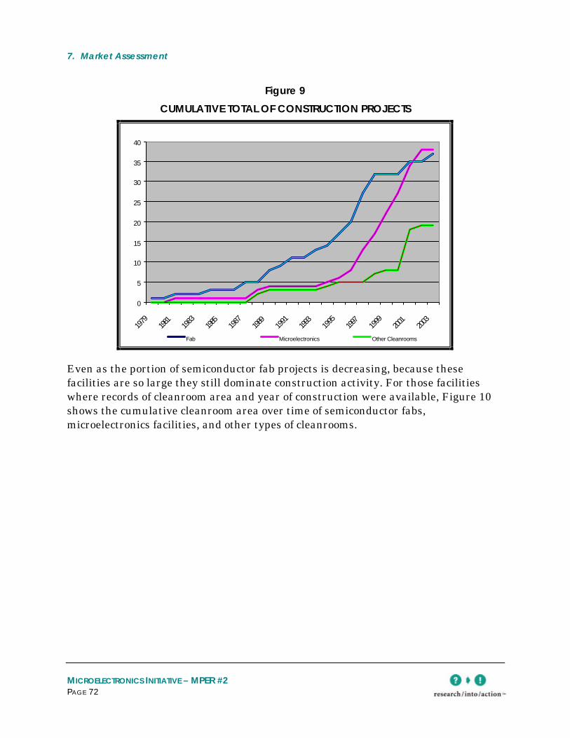
7. Market Assessment
MICROELECTRONICS INITIATIVE – MPER #2 PAGE 72
Figure 9
CUMULATIVE TOTAL OF CONSTRUCTION PROJECTS
0
5
10
15
20
25
30
35
40
1979
1981
1983
1985
1987
1989
1991
1993
1995
1997
1999
2001
2003
Fab Microelectronics Other CleanroomsFab Microelectronics Other Cleanrooms
Even as the portion of semiconductor fab projects is decreasing, because these facilities are so large they still dominate construction activity. For those facilities where records of cleanroom area and year of construction were available, Figure 10 shows the cumulative cleanroom area over time of semiconductor fabs, microelectronics facilities, and other types of cleanrooms.

7. Market Assessment
MICROELECTRONICS INITIATIVE – MPER #2 Page 73
Figure 10
CUMULATIVE CLEANROOM AREA BY CATEGORY
0
500,000
1,000,000
1,500,000
2,000,000
2,500,000
1979
1981
1983
1985
1987
1989
1991
1993
1995
1997
1999
2001
2003
Fab Microelectronics Other Cleanrooms
Market Trends
We developed an assessment of possible near-term futures of the semiconductor fab and microelectronics industries. As noted in the first MPER, the majority of these firms conduct their business worldwide. This is particularly important to consider for the future of this market, especially for semiconductor manufacturers. These firms make decisions on plant operation, production, and sometimes even staffing without being bound to any geographic location. These companies are truly worldwide and are looking to build and operate facilities anywhere it makes economic sense.
Another major factor to consider when seeking understanding of the future of microelectronics in the region is that the industry is opaque; plans for plant closures, expansions, sales, or purchases are seldom described publicly before they are well underway. Still, the experts we spoke with have substantial experience and numerous confidential contacts, and have confidence in their knowledge of industry activity.
The general market size for semiconductor fabs in 2003 is about 1,100 facilities worldwide. Worldwide closures of fabs have numbered 209 since 1990, with 62 of

7. Market Assessment
MICROELECTRONICS INITIATIVE – MPER #2 PAGE 74
these shutting down in 2001. Construction was started on $50 billion worth of semiconductor fabs in 2000, while in 2001, construction starts were down to $12 billion; in 2002, start investments recovered to $22 billion.
Our industry experts believe that construction of cleanrooms for general purposes is growing much more rapidly than construction of semiconductor fab facilities. Although construction activity in the U.S. has essentially come to a standstill for the past two years, over the past five years, the growth in the number of cleanroom projects other than fabs has averaged about 15% annually, about five times the recent increase in the number of fabs.
The experts also noted that considerations for process tool efficiency are of much less interest to semiconductor firms relative to facility efficiency. This is in part because of the rapid turnover of process tools (changing every two or three years for cutting-edge facilities), but more importantly because there is greater acceptance by the microelectronics industry of facility improvements.
In general, the global market for production of semiconductor products has shifted away from US production to Asia, and especially to China. China has significant demand of its own and low production costs, and is the focus for most of the new semiconductor fab construction, with perhaps two fabs per year being built there over the next ten years.20 It is expected that 80% of all semiconductor fab construction spending for the near-term will be in Asia and China. The remaining 20% is for the entire rest of the world.21
The general view of the Pacific Northwest region by the experts we spoke with is that the Pacific Northwest is at a competitive disadvantage at this time, specifically when compared to production in Asia. One focused view is that some fab activity in the Pacific Northwest will come from smaller foundries that would either retrofit existing fab facilities or take over existing production lines if they were intact.
Some companies are moving now to outsourcing their production and using foundries to build their chips. Motorola is an example—while they once had an annual capital budget of $2 billion for fabs, that budget is now down to $200 million and they have outsourced some of their production.
20 Presentation at 20th Annual State of the Industry, SEMICON West, San Francisco, CA, July 2002.
21 Interview with George Burns, 12/24/2002.

7. Market Assessment
MICROELECTRONICS INITIATIVE – MPER #2 Page 75
Foundries have been taking a bigger share of the chip market since about 1995. “Fabless” semiconductor companies have become a successful business model, where integrated device manufacturers (like Motorola) get production capacity without the need to make major capital investments. A number of medium-sized semiconductor companies are now being faced with the decision to abandon their fabs and go to foundries for production – they might perhaps sell their fabs to a foundry firm while retaining an option for a fraction of the fab capacity.
Major processor companies like Intel, companies that manufacture memory, and other integrated device manufacturers such as IBM will likely always have their own manufacturing capability. For these types of businesses, manufacturing for themselves provides a competitive advantage and the ability to remain on the cutting edge. They can offer the highest performance for the highest margins, or in the case of memory, to be able to compete on price/performance tradeoffs from their manufacturing efficiency.
Location Choice Drivers
As the general economy improves, it is expected that the recovery will filter down to microelectronics in the Pacific Northwest region. Currently our observers are seeing a weak recovery in the semiconductor industry. This recovery is weak because it is not driven by a major end-user demand as has happened in past recovery cycles. Until there is the next hot new product that drives end-user demand, these experts do not anticipate a significant recovery.
The Pacific Northwest as a region is perceived as one of the better places in the world to build and operate semiconductor fabs. With high quality of life, availability of skilled labor, and competitive electric power and water costs, these factors have been a consideration for some companies’ decision-making. In addition, economic incentives from local or state governments are seen as the biggest drivers for location decisions, perhaps even more important than availability of existing facilities.
Besides labor and quality of life, another regional attraction is our local educational institutions that provide research for development of new technologies. Also important are other local infrastructure issues for fabs, such as the presence of major wafer manufacturers like Wacker Siltronic and SEH America, permitting chipmakers to more easily work with important suppliers. Polysilicon is also a local product for which there are not many worldwide suppliers, another infrastructure benefit for the region.
7. Market Assessment
MICROELECTRONICS INITIATIVE – MPER #2 PAGE 76
Time-to-market is a critical issue – companies can take advantage of market cycles by getting into production quickly. The smaller semiconductor companies may not move the market, except that they may be able to buy and cost-effectively produce in a used fab. For companies that do not make advanced chips, a used 8-inch production line is a reasonable technology acquisition.
Some of the used fabs on the market today are incredible bargains. This is especially true if the owners have maintained the cleanrooms, if production tools are intact, and if the facility remains licensed and permitted. Facilities like this provide a great time-to-market advantage. Those facilities that are half-finished or decommissioned are not as attractive, but still may provide capacity in a few months rather than the year or two that greenfield construction can take.22
Although energy is the largest operational cost for the semiconductor industry, it is dwarfed by both capital expenditures and, more importantly, by revenues. Our experts do not see energy costs alone being a driver for location choices in the semiconductor industry – the real estate market has not observed any particular interest regarding electric power rates for recent location decisions. However, it is believed that facilities designed and engineered for efficiency and environmental friendliness would have a stronger position in the market. A few companies are establishing a policy or position of being environmentally responsible or “green,” and therefore energy and water efficiency may be important to their location decisions.23 Still, it is interesting to note that, in regards to environmental responsibility, while the semiconductor industry as a whole has established forums to discuss reducing emissions of global warming gasses from their own production, they have not included consideration of the same gases from electricity generation.24
Outlook for 2004
Our discussions with experts (cited above) and with our regional contacts (described in Chapter 6) suggest that no new semiconductor production fabs will be built in the Pacific Northwest in the next few years. This is a significantly different vision than what was seen in 1996, when the Alliance first funded the Microelectronics Initiative.
22 Let’s Make a Deal, Oregon Business, November 2002.
23 For example, Intel’s statement on global climate change can be found at http://intel.com/intel/other/ehs/Globalclimate.htm.
24 Personal interview at SEMICON West, San Francisco, CA, July 2002.

7. Market Assessment
MICROELECTRONICS INITIATIVE – MPER #2 Page 77
At that time, the prediction was that three to five semiconductor fabs would be built in the region annually.
In addition, no major fab closures are expected in the region over the next two years. Ownership turnover will likely be a significant driver in the market in this period. What seems to be an attraction for microelectronics locating in the Pacific Northwest is the potential for adaptive reuse of existing facilities. For example, one that could turnover is the Microchip/Matsushita facility in Puyallup, Washington, which may be purchased and reequipped by a foundry.
If the highest and best use of a facility cannot be fulfilled—for example a dedicated fab being purchased by a foundry—cleanrooms might be converted for other microelectronics, or even for use by the biomedical, biotechnology, or pharmaceutical industries.
In addition to turnover of ownership in some facilities, it is believed that there may be one or two small ($100-$200 million) fab facilities that could be built by mid-sized companies that do not have a worldwide presence. It is not believed that in the next two years any larger fabs will be started. And although it is not in the Pacific Northwest region, it is significant that in this time period, Micron may choose to go forward and install tools to produce memory in their Lehi, Utah facility.
During this time, Intel is expected to being equipping their D1D fab, and their D1C facility will become a 300-mm production line. And just past the 2004 window might be a time that Intel would began development work on a new fab in the Pacific Northwest.
Although cleanrooms for other microelectronics industries (besides fabs) have lower energy intensity compared to semi fabs, and are smaller facilities, they will probably continue to be built as greenfield projects or as plant expansions at several times the rate of fabs in the next few years. This is likely also true for the biomedical and pharmaceutical industries, as well as for research labs.
Outlook for 2007
Although 2007 is difficult to prognosticate, our experts do not see any further contraction in capacity in the Pacific Northwest. It is believed that a new fab might be built in the Eugene area, and a major facility of one or two billion dollars may be located somewhere in the region. This major expansion could be built by an established company, or perhaps by a foundry that wants a facility here. In any case,

7. Market Assessment
MICROELECTRONICS INITIATIVE – MPER #2 PAGE 78
siting of any of these major investments will likely involve some incentives such as tax breaks. It is also likely that any fabs that are deemed marginal by their owners will be sold and refitted rather than closed and decommissioned.
As mentioned for 2004, Intel may have plans to build another developmental fab or other facility in the Pacific Northwest; and Micron will continue to build fabs in the US, perhaps locating in the Pacific Northwest, but away from their headquarters in Boise. Although building a fab in Asia is attractive for many reasons, locating in the Pacific Northwest will remain a consideration as both customers and suppliers are here, a major logistical advantage.
And as described for 2004, other microelectronics and the biomedical and pharmaceutical industries should continue to be significant in the number of regional projects built as compared to semi fabs, if not in cleanroom area or in energy use.
COST-EFFECTIVENESS RECOMMENDATIONS
Introduction
As part of the review of the Microelectronics Initiative, the evaluators have examined the assumptions upon which the Initiative’s initial cost-effectiveness calculations were based. These original assumptions were developed by Alliance staff from the Intel Fab 15 case study and MPER #1.
For our recommendations, we have relied on information gathered from Special Projects Fund work with Intel, H-P, and Zilog that was implemented by the Initiative, and on actual conditions and projections of market size and share as summarized in the section above. The adoption of any recommendations to revise assumptions for the cost-effectiveness calculations should be the result of collective decision-making by the Alliance and the evaluation team.
Cost-Effectiveness Assumptions and Recommendations
Cost-effectiveness assumptions refer to those factors that directly affect the overall estimates of program viability. The major inputs currently used by the Microelectronics Initiative are shown in the second column of Table 21.

7. Market Assessment
MICROELECTRONICS INITIATIVE – MPER #2 Page 79
Recommendations for changes to be made to the original cost-effectiveness assumptions are also presented in Table 21, in the third column. A discussion of each of the recommendations follows the table.
Table 21
SUMMARY OF RECOMMENDATIONS FOR CHANGES TO ASSUMPTIONS
CE INPUT ORIGINAL ASSUMPTION
RECOMMENDATION
Cost-effectiveness Unit Small-sized Semiconductor
Fabrication Facility
Average-sized Semiconductor
Fabrication Facility
Total Number of Facilities in 2001 82 44
Total Number of Facilities in 2010 162 47
Initiative Projects by 2002 2 3
Market Effect Projects 2003-2010 39 20
Facility Energy Use, kWh/Year 29,100,110 100,000,000
Measure Lifetime, Years 10 years 10 years
Non-Energy Benefits Savings/Year $0 (assumed) $0 (likely non-zero)
Efficiency Improvement 10% 10%
Facility Efficiency Savings, kWh/Year 2,900,000 10,000,000
Periodic O&M Cost/Facility/Year $0 $0
First Costs $350,200 $350,200
Consumer Costs $241,408 $241,408
Project Size & Facility Energy Use
It is recommended that the initial cost-effectiveness unit of a small-sized semiconductor fabrication facility be revised. Originally, this may have been set to

7. Market Assessment
MICROELECTRONICS INITIATIVE – MPER #2 PAGE 80
the size of Intel’s Fab 15, which has 20,000 square feet of cleanroom in an 82,000 square foot facility. The average size of a microelectronics fab facility in the Pacific Northwest is several times larger, at 295,000 square feet overall, with 60,000 square feet of cleanroom.
Facility energy use is proportionally higher for an average-sized fab, at 100,000,000 kWh annually.25
Number of Facilities
The market assessment performed by Research Into Action identified 44 semiconductor fabrication facilities in the Pacific Northwest. With the industry in its current recession, it is difficult to project growth. Still, it is believed that there is a worldwide structural change that will limit new fabs both in the region and in the U.S. So we have assumed that by 2010 there would be the equivalent of 47 average-sized fabs in the region, a very modest growth of a new fab every two years. We recommend that this forecast be reviewed at least biannually.
Initiative & Market Effect Projects
There have been three Initiative Special Projects implemented to date. We believe that more demonstration projects such as these will be appropriate to move the industry toward consistent application of operational and capital investments in energy efficiency. Again, with the industry in its current recession and flux, it is difficult to project market effects. However, we have assumed that one-third of the total market may make changes due to the Initiative.
Capital Costs
Although the Special Projects pursued to date have almost exclusively implemented no-cost and low-cost measures, we do not believe that this will necessarily be true for future projects. Implementation costs in fabs for efficiency measures that require
25 Also supported by average values of 1,450 kWh/cleanroom square-foot/year from E-Source. Delivering Energy Services to Semiconductor and Related High-Tech Industries: Part 1: Market Assessment . January 1998.
7. Market Assessment
MICROELECTRONICS INITIATIVE – MPER #2 Page 81
capital can be quite high, and so for the time being we recommend no change to the capital cost inputs.
Operation and Maintenance Costs
Operation and maintenance costs are to be paid by the facilities for keeping implemented measures up to date and working effectively to ensure savings persistence. Since measures used so far have been operational changes at no-cost or low-cost, the initial value of zero for operation and maintenance costs seems appropriate.
Lifetime of Measure
The lifetime of the project measures is still assumed to be ten years.
Efficiency Improvement
The energy savings achieved to date by the Special Projects appear to be approximately that assumed in the original cost-effectiveness analysis and, at this point in time, we do not recommend a change. However, this is a critical value for cost-effectiveness, and the engineering reports reviewed from the Special Projects do not consistently report savings in the same manner as used in the analysis. We will review engineering reports while they are being developed for future projects to see if this value should be revised.
Non-Energy Benefits
It is likely that some measures will have benefits beyond energy savings alone. For example, occupancy-based recirculation airflow setback reduces particle counts as well as energy use. If there are monetary benefits from non-energy benefits, they will need to be documented before they would be recommended for inclusion in the cost-effectiveness analysis.
Program Expenditures
Program expenditures are also included in cost-effectiveness assumptions. Cost information is still being developed based on actual invoiced amounts. Once developed these will be included in future cost effectiveness tables.

7. Market Assessment
MICROELECTRONICS INITIATIVE – MPER #2 PAGE 82

MICROELECTRONICS INITIATIVE – MPER #2 PAGE 83
8. FINDINGS AND RECOMMENDATIONS
The Microelectronics Initiative is a collection of efforts to facilitate market transformation in the broad microelectronics industry of the Pacific Northwest. This MPER examines progress in several of these efforts:
Ø Workshops sponsored by the Alliance and offered to Pacific Northwest microelectronics firms on energy efficiency issues;
Ø Three projects for demonstration and benchmarking of energy savings opportunities in the chilled water plants at semiconductor fabrication facilities;
Ø A co-funded project by Lawrence Berkeley National Laboratories (LBNL) to develop design guidelines for cleanrooms;
Ø The ASiMI Dendritic Polysilicon Production project to develop a smaller sized polysilicon product that is both more energy efficient to produce and more easily used in recharge applications, reducing energy consumption for the product user as well; and
Ø The H-P Design Charette to identify energy efficient retrofit opportunities for implementation in the renovation of an existing semiconductor fabrication facility.
This MPER also includes an updated market assessment focused specifically on microelectronics firms located in the Pacific Northwest.
The results of this investigation provide sound evidence that the Alliance efforts are having an effect on the microelectronics industry in the Pacific Northwest. The results also suggest that there remain opportunities for market transformation. The following conclusions and recommendations are offered for consideration.
Finding 1
The workshops sponsored by the Alliance, are a very effective market transformation tool. This is backed by strong evidence from workshop attendees and from the fact

8. Findings and Recommendations
MICROELECTRONICS INITIATIVE – MPER #2 PAGE 84
that two of the three special fund projects and the H-P design charette emerged in large part as a result of the firms’ experience with the workshops.
Recommendation 1
Continue offering one workshop per year. The next workshop could offer presentations on the results of the three special projects, especially a comparison of them, as well as a report on the H-P design charette. Workshop participants also offered a host of ideas for additional topics: discussion of air flow improvements, chiller and chilled water improvements, compressed air, ways to sell efficiency to management, and others described in Tables 3 and 6.
Finding 2
The Special Projects Fund approach has identified and implemented a significant number of energy efficiency measures in semiconductor fabs. Although the availability of funding from the Alliance was an attraction to undertake the special projects, the implemented measures were no-cost and low-cost, and many have achieved substantial energy savings.
Recommendation 2
The Special Projects Fund has led to important upgrades in efficiency in semiconductor fabs. The Alliance should move to quickly publicize these results. In addition to presenting them in a workshop, the Alliance should create case studies to further promote and disseminate information on the efficiency measures that were implemented and the results of the project efforts.
Finding 3
The H-P design charette was extremely effective in achieving specific savings for the plant and in influencing internal behavior to consider energy efficiency ideas, such as design charettes, for future projects.
Recommendation 3
Charettes can provide an effective means to influence plant design. The keys to success are being able to meet the design timeline, providing knowledgeable

8. Findings and Recommendations
MICROELECTRONICS INITIATIVE – MPER #2 Page 85
experts to participate in the charette, providing documentation of the analysis that can be used for presentation to management or to organizations with incentives, and becoming involved in the project early enough to influence some design decisions as well as conducting a project review just prior to construction completion to ensure that operational measures are incorporated in the plant start-up.
Finding 4
The ASiMI project at Moses Lake, Washington, and at Butte, Montana, appears to provide a clear example of local energy conservation. The market transformation effects appear to be limited. This is both because of the joint venture, which splits ASiMI production into either solar grade or semiconductor grade, and the fact that at this time neither grade appears likely to result in changes in recharge behavior on the part of the semiconductor industry, where the greatest savings are possible. In addition, the current industry slump is not conducive to firms doing more than exploring their options so no changes in behavior are likely to occur until the industry rebounds.
Recommendation 4
Continue to monitor industry response to the ASiMI products—teardrop and teardrop plus.
Finding 5
The market assessment uncovered a large potential common market in cleanrooms between microelectronics and other industries, such as biomedical, pharmaceutical and other electronic sectors. Clearly the cleanliness requirements for semiconductor fab cleanrooms are much more restrictive and result in higher energy consumption, yet the growth in other cleanrooms is substantial and likely to continue at a higher pace than in the semiconductor arena. Reaching all sectors regarding efficiency in cleanrooms may improve opportunities in the microelectronics industry itself, as well as spread the effects of the Initiative more widely throughout the region.
Recommendation 5

8. Findings and Recommendations
MICROELECTRONICS INITIATIVE – MPER #2 PAGE 86
Consider exploring the common aspect of cleanrooms and solutions for improving the energy efficiency of all cleanrooms as a market transformation opportunity for multiple industries.
Finding 6
There are some indications that energy efficiency may play a small part in decisions to purchase semiconductor fabs. With investments in new PNW semiconductor fabs over the next few years being limited, there may be opportunity to affect efficiency change when existing facilities are turned over to new ownership.
Recommendation 6
Consider exploring the possibility of marketing energy impacts and efficiency for selection of closed or for sale microelectronics facilities.
MICROELECTRONICS INITIATIVE – MPER #2
APPENDICES

Appendices
MICROELECTRONICS INITIATIVE – MPER #2

MICROELECTRONICS INITIATIVE – MPER #2
APPENDIX A
Interview Guide for Microelectronics Initiative Alliance Workshops

Appendix A
MICROELECTRONICS INITIATIVE – MPER #2

MICROELECTRONICS INITIATIVE – MPER #2 PAGE A - 1
INTERVIEW GUIDE FOR MICROELECTRONICS INITIATIVE ALLIANCE WORKSHOPS (N=30)
Hello, my name is _________________. I understand that you have attended a workshop sponsored by the Northwest Energy Efficiency Alliance on energy efficiency in the microelectronics industry. I am doing research help the Alliance assess the value of the workshops to participants and give the Alliance input to decide whether they should continue to give these workshops. [Interviewer, if necessary: This isn’t the first evaluation we’ve done. You may have talked to my colleague Jane Peters. This is a follow-up evaluation.]
Q1
Which of the three Alliance-sponsored workshops did you attend? [Note: workshops were held January 19, 1999; May 3, 2000; May 22, 2001.]
Q2
Did you do a presentation at one of the workshops or were you an attendee?
Q3
Would you say that attending the workshops increased your awareness of the importance or benefits of energy efficiency?
Ø Your interest in or enthusiasm for energy efficiency?
Ø Did the workshop provide you with any new ideas or ways of thinking about energy?
Ø Did the information presented address any of the concerns that you may have had about moving to greater efficiency?

Appendix A
MICROELECTRONICS INITIATIVE – MPER #2 PAGE A - 2
Q4
Since the workshop, have you discussed any of these ideas with others in your firm?
Ø Have any of your suggestions been implemented or taken into serious consideration?
[If no:] Why not?
[If yes:] What happened?
Q5
Can you provide any feedback on what you liked and disliked about the workshops?
Q6
Would you go again?
Ø Would you recommend them to others?
Q7
Would you encourage the Alliance to hold more of these workshops?
[If yes:]
Ø What topics would you like to hear about?
Ø Would you be interested in an annual workshop or less often?
Q8
Are you aware of the Design Guidelines for Clean Rooms prepared by LBNL?
[If no>] Go to Industry Perspectives

Appendix A
MICROELECTRONICS INITIATIVE – MPER #2 PAGE A - 3
Q9
Are you involved in any aspect of clean room design that might relate to the guidelines?
[If no>] Go to Industry Perspectives
Q10
Have you used them?
[Yes:] What was experience?
How can they be improved?
[No:] Would you?
[Yes:] Any barriers to doing so?
[No:] Why not?
INDUSTRY PERSPECTIVES
Are you able to talk a few more minutes about trends in the industry?
Q11a
How would you say the microelectronics industry has changed in the past three years?
(Probe: Explore changes in economic context, technologies used. Distinguish between operations and process changes)
Q11b
How do you see future growth in the Pacific Northwest compared to elsewhere in the US and in the world?

Appendix A
MICROELECTRONICS INITIATIVE – MPER #2 PAGE A - 4
Q12
Has there been a change in the attention paid to energy use from three years ago?
[If change:] Would you say that the Alliance has had a positive influence on this change? Why do you say that?
Q13
What gets in the way of addressing energy use? (Probe: in operations, in process, in other aspects) (Probe: what are the objections? Who raises these objections? Are any managerial systems getting in the way?)
Q14
Is there any way that the Alliance can address these stumbling blocks?
Q15
I’ve just a few more questions. Is it okay to continue?
Q16
The International Technology Roadmap for Semiconductors foresees a 20% to 50% reduction in both facility and equipment electricity use per cm2 of production in the next 5 years. Do you see this coming more from product and productivity improvements (such as chip densities or higher yields) or greater energy efficiency in production? Any specific areas?
Q17
What type of firm do you think leads innovation in process or efficiency improvements, or who is looked to for advice? Would you say it’s the semiconductor firms, or the consulting engineers, or perhaps equipment manufactures?

Appendix A
MICROELECTRONICS INITIATIVE – MPER #2 PAGE A - 5
Q18
Considering each of the following segments, what proportion (rough is okay) of the market would you say has been reached by the Alliance?
Ø Semiconductor firms in the PNW,
Ø Designers and consulting engineers in the PNW,
Ø Process equipment manufacturers in the PNW
Ø Product manufacturers in the PNW
That was the last of my questions, thank you for your time.

Appendix A
MICROELECTRONICS INITIATIVE – MPER #2 PAGE A - 6

MICROELECTRONICS INITIATIVE – MPER #2
APPENDIX B
Interview Guide for Microelectronics Initiative Exploration of Special Projects

Appendix B
MICROELECTRONICS INITIATIVE – MPER #2

MICROELECTRONICS INITIATIVE – MPER #2 PAGE B - 1
INTERVIEW GUIDE FOR MICROELECTRONICS INITIATIVE EXPLORATION OF SPECIAL PROJECTS (N=6)
(Key: Eng = ask of consulting engineers; Mfg = ask of semiconductor manufacturers)
Q1
What is the current status of the project?
(Probes: Expected completion date. What was recommended? What was/will be installed? What were the criteria for accepting recommendations? What is the status of installations?)
Q2
Have you seen the energy savings you were expecting?
Q3
Have there been any other benefits from the project, like production or process changes, labor savings, ongoing monitoring capability?
Q4
Were there any unexpected downsides to the project?
Q5
[Eng:] What gets in the way of firms buying into a project like this? Moving ahead with recommendations?
[Mfg:] Did any of the concerns you had about possible negative impacts of the project happen? [Probes:] How about impact to production? On health or safety? On the amount of your time that would be required? Anything other objections or concerns that were raised at the outset?

Appendix B
MICROELECTRONICS INITIATIVE – MPER #2 PAGE B - 2
[If any impacts:] Were you satisfied how they were handled?)
Q6
What was it that made this project happen? Would the project have been of interest to management without Alliance funding or involvement? (Probes on “involvement”: initiating the idea, bringing people together, endorsing the concept)
Q7
How long did the project take from the time it was proposed to completion? [If several years:] What factors led it to take so long?
Q8
Did the project go as smoothly as you expected? What could the Alliance have done to make the project go more smoothly? (Probes: project management, problem solving, making sure people meet their commitments)
Q9
Given the challenges to do a project like this and your experience with this one, what resources are needed to facilitate future projects like this?
Q10
[Eng:] Is the project approach going to be applied to any other plants at that facility or for that client? Is it under consideration? What were the reasons this is being or is not being done?
[Mfg:] How aware are others in your company about the project? Do the people who are charged with constructing new plants know about this? How about the designers your firm typically uses for new construction projects?

Appendix B
MICROELECTRONICS INITIATIVE – MPER #2 PAGE B - 3
Q11 [Mfg]
Is the project approach going to be applied to any other plants in your company or other buildings at your facility? Is it under consideration? What were the reasons this is being or is not being done?
Q12
[Eng:] Have you had any success in selling same/similar services to other microelectronic firms? Where? What is the level of market interest in this or similar projects?
[Mfg:] How satisfied are you with the project? Have you recommended the project to others?
[If yes:] Who? (Within or external to company)
[If no:] Would you?
Q13 Eng
Have you had any success in selling these services to other types of firms? Has your business grown? Do you have any competitors?
Q14
How would you say the microelectronics industry has changed in the past three years?
(Probe: Explore changes in economic context, technologies used. Distinguish between operations and process changes.)
Q15
Has there been a change in the attention paid to energy use from three years ago?
[If change:] Would you say that the Alliance has had a positive influence on this change? Why do you say that?

Appendix B
MICROELECTRONICS INITIATIVE – MPER #2 PAGE B - 4
Q16
What gets in the way of addressing energy use? (Probe: in operations, in process, in other aspects) (Probe: what are the objections? Who raises these objections? Are any managerial systems getting in the way?)
Q17
Is there any way that the Alliance can address these stumbling blocks?
Q18
How are we doing for time? Is it okay to continue?
Q19
The International Technology Roadmap for Semiconductors foresees a 20% to 50% reduction in both facility and equipment electricity use per cm2 of production in the next 5 years. Do you see this coming more from product and productivity improvements (such as chip densities or higher yields) or greater energy efficiency in production? Any specific areas?
Q20
What type of firm do you think leads innovation in process or efficiency improvements, or who is looked to for advice? Would you say it’s the semiconductor firms, or the consulting engineers, or perhaps equipment manufactures?
Q21
Considering each of the following segments, what proportion (rough is okay) of the market would you say has been reached by the Alliance?
Ø Semiconductor firms in the PNW,
Ø Designers and consulting engineers in the PNW,
Ø Process equipment manufacturers in the PNW

Appendix B
MICROELECTRONICS INITIATIVE – MPER #2 PAGE B - 5
Ø Product manufacturers in the PNW
IF THESE CONTACTS ALSO PARTICIPATED ALLIANCE WORKSHOPS:
Q23
How many of the three Alliance-sponsored workshops did you attend? [Note: workshops were held January 19, 1999; May 3, 2000; May 22, 2001.]
Q24
Did you do a presentation at one of the workshops or were you an attendee?
Q25
Would you say that attending the workshops increased your awareness of the importance or benefits of energy efficiency?
Ø Your interest in or enthusiasm for energy efficiency?
Ø Did the workshop provide you with any new ideas or ways of thinking about energy?
Ø Did the information presented address any of the concerns that you may have had about moving to greater efficiency?
Q26
Since the workshop, have you discussed any of these ideas with others in your firm?
Ø Have any of your suggestions been implemented or taken into serious consideration?
[If no:] Why not?
[If yes:] What happened?

Appendix B
MICROELECTRONICS INITIATIVE – MPER #2 PAGE B - 6
Q27
Can you provide any feedback on what you liked and disliked about the workshops?
Q28
Would you go again?
Ø Would you recommend them to others?
Q29
Would you encourage the Alliance to hold more of these workshops?
[If yes:]
Ø What topics would you like to hear about?
Ø Would you be interested in an annual workshop or less often?
LBNL DESIGN GUIDELINES FOR CLEAN ROOMS (ASK OF WORKSHOP PARTICIPANTS)
Q30
Are you aware of the Design Guidelines for Clean Rooms prepared by LBNL?
[If no>] Go to Industry Perspectives
Q31
Are you involved in any aspect of clean room design that might relate to the guidelines?
[If no>] Go to Industry Perspectives
Q32
Have you used them?

Appendix B
MICROELECTRONICS INITIATIVE – MPER #2 PAGE B - 7
[Yes:] What was experience?
How can they be improved?
[No:] Would you?
[Yes:] Any barriers to doing so?
[No:] Why not?

Appendix B
MICROELECTRONICS INITIATIVE – MPER #2 PAGE B - 8

MICROELECTRONICS INITIATIVE – MPER #2
APPENDIX C
Interviews for H-P Design Charette

Appendix C
MICROELECTRONICS INITIATIVE – MPER #2

MICROELECTRONICS INITIATIVE – MPER #2 PAGE C- 1
INTERVIEWS FOR H-P DESIGN CHARETTE
Date ________________________
Name _________________________________________________________________
Company ______________________________________________________________
E-Mail ______________________________Phone ____________________________
The purpose of this interview is to learn what your experience was with the design charette in February. These questions concern whether the information you got from the charette has affected the project you were working on, whether it affected any other projects and how you would assess the value of the charette.
THIS INTERVIEW GUIDE IS FOR PARTICIPANT FIRMS
For Rumsey
What did you do after the charette regarding the different three “ideas”? (What type of work did you do on them, design – analysis – something else? Did they all get developed? Did any get dropped, if so why?)
What did you feel that the response from IDC and HP was to the ideas you worked on?
What is your assessment of the charette in terms of the ability of the charette to get new ideas into the design discussion and have them seriously considered?

Appendix C
MICROELECTRONICS INITIATIVE – MPER #2 PAGE C- 2
For IDC
What did you do after the charette regarding the different twenty-three “ideas” for which your team was going to conduct NPV analysis? (Did you do the analysis for all of them? Did any get dropped, if so why?)
What about the four “ideas” that were viewed as “best practice”? (Did you integrate these into the HP project? Have you integrated them into other projects? Have you discussed them with other members of your company?)
What did you feel that the response was to the ideas you worked on?
For HP and IDC
What did you do with the information provided by Rumsey?
Which ideas were eventually incorporated into the design? Why?
Which ones were not and why?
Have any of these ideas been considered for another project either for HP or for another client?
What is your assessment of the charette in terms of the ability of the charette to get good ideas into the discussion and have them seriously considered?

Appendix C
MICROELECTRONICS INITIATIVE – MPER #2 PAGE C - 3
Ask Everyone:
Have you discussed this charette with any of your colleagues?
What have you told them about the charette?
What do you think could be done to improve the charette?
What type of situation do you think would be useful for a future charette?
THIS INTERVIEW GUIDE IS FOR NEEA STAFF, BILL TSCHUTTI AND TOM HANZ
NEEA Staff
How did the design charette come about? (Were you surprised at the interest, given the earlier lukewarm reception to the idea? What do you think led to the openness?)
What were your objectives in conducting the charette?
Consultants
What were your expectations for the HP design charette?
How did the HP charette differ or compare to other charettes you have been involved in?
Appendix C
MICROELECTRONICS INITIATIVE – MPER #2 PAGE C- 4
NEEA and Consultants
What is your perception of what happened during the charette?
Ø Do you think the participants were open to new ideas?
What do you think happened as a result of the charette?
Ø What results have you seen?
What do you think was the weakest part of the charette?
What would you do to improve it?
What was the strength of the charette?

P.O. Box 12312, Portland, Oregon 97212
503 / 287-9136