micom p543; p544; p545 & p546 - current differential ......micom p543, p544, p545 & p546...
TRANSCRIPT

MiCOM P543, P544, P545 & P546 Current Differential Protection Relay
P54x/EN M/Ka4+Kb4 Software Version 45, 47, 55 & 57 Hardware Suffix K
Technical Manual Contains: P54x/EN AD/Kb4 V47 & 57 K Addendum P54x/EN M/Ka4 V45 & 55 K Manual

Note: The technical manual for this device gives instructions for its installation, commissioning, and operation. However, the manual cannot cover all conceivable circumstances or include detailed information on all topics. In the event of questions or specific problems, do not take any action without proper authorization. Contact the appropriate Schneider Electric technical sales office and request the necessary information.
Any agreements, commitments, and legal relationships and any obligations on the part of Schneider Electric including settlements of warranties, result solely from the applicable purchase contract, which is not affected by the contents of the technical manual.
This device MUST NOT be modified. If any modification is made without the express permission of Schneider Electric, it will invalidate the warranty, and may render the product unsafe.
The Schneider Electric logo and any alternative version thereof are trademarks and service marks of Schneider Electric.
All trade names or trademarks mentioned herein whether registered or not, are the property of their owners.
This manual is provided for informational use only and is subject to change without notice.
© 2010 Schneider Electric. All rights reserved.

MiCOM P543, P544, P545 & P546 Current Differential Protection Relay
P54x/EN AD/Kb4
Software Version 47 & 57 Hardware Suffix K
Update Documentation

Note: The technical manual for this device gives instructions for its installation, commissioning, and operation. However, the manual cannot cover all conceivable circumstances or include detailed information on all topics. In the event of questions or specific problems, do not take any action without proper authorization. Contact the appropriate Schneider Electric technical sales office and request the necessary information.
Any agreements, commitments, and legal relationships and any obligations on the part of Schneider Electric including settlements of warranties, result solely from the applicable purchase contract, which is not affected by the contents of the technical manual.
This device MUST NOT be modified. If any modification is made without the express permission of Schneider Electric, it will invalidate the warranty, and may render the product unsafe.
The Schneider Electric logo and any alternative version thereof are trademarks and service marks of Schneider Electric.
All trade names or trademarks mentioned herein whether registered or not, are the property of their owners.
This manual is provided for informational use only and is subject to change without notice.
© 2010, Schneider Electric. All rights reserved.

Update Documentation P54x/EN AD/Kb4-S
MiCOM P543, P544, P545 & P546
(AD) -1
UPDATE DOCUMENTATION

P54x/EN AD/Kb4-S Update Documentation
(AD) -2
MiCOM P543, P544, P545 & P546

Update Documentation P54x/EN AD/Kb4 MiCOM P543, P544, P545 & P546
(AD) -3
P54x UPDATE DOCUMENTATION In the firmware version 45 and 55K of P54x, several changes on existing features have been added. These are described with reference to the documentation listed below:
Release Version Documentation 16.03.2009 P54x/EN M/Ka4 Technical Manual
Document Ref. Section Page No. Description
P54x/EN IT/Ga4
3.1
1-7
Functional overview 64 REF protection added Corrected 67/46 to show 4 stages
3.2
1-10 1-11
Ordering options Hardware options updated Redundant Etherner Options added Software number updated
P54x/EN TD/Ja4
-
2-7
Protection functions Phase and ground (earth) Overcurrent modified to Three Phase Overcurrent Protection. Addition of Accuracy claims. Earth Fault added REF Added
-
2-12 2-15
Settings, measurements and records list Configuration updated EIA(RS)232 Teleprotection added INTERMiCOM conf. added Prot comms/IM64 updated
-
2-17 2-19
Protection functions Phase current differential protection updated Sensitive earth fault updated
-
2-24 2-26
Measurements list Measurements 1 updated Fault Record Proforma updated
P54x/EN ST/Ba4
1.1
4-4
4-6
Relay settings configuration Sensitive E/F modified to SEF/REF PROT’N IREF>Stage added Restricted Earth Fault Protection added Read Only mode feature added
1.2
4-6
Integral teleprotection settings New section
1.2.1
4-6
EIA(RS)232 InterMiCOM New section
1.3
4-8
Protection communication configuration GPS Sync updated Char Mod Time updated Char Mod Ex feature added Char Mod Ex Time feature added
1.4.2
4-17
Distance setup (only for models with distance option) Cells under DELTA DIRECTION updated

P54x/EN AD/Kb4-S Update Documentation
(AD) -4
MiCOM P543, P544, P545 & P546
Document Ref. Section Page No. Description P54x/EN ST/Ba4 Continued
1.4.4
4-23
Phase differential Compensation: Vector group text changed to Transformer Inrush Restraint updated to add blocking feature Ih (2) & (5) features added Id High Set updated
1.4.12
4-38
4-39
Sensitive earth fault Sensitive E/F modified to SEF/REF HI Z REF Protection added IREF> Is setting added
1.5.1
4-68
System data Software Ref.1 and 2 updated
P54x/EN OP/Ba4
1.1.1.2
5-18
Time alignment of current vectors with GPS input (all models) Section updated to reflect changes to GPS SYNC setting.
1.2
5-20
Protection of transformer feeders (P543 and P545) Previously 1.1.4 Section updated
1.2.1
5-20
Enabling or disabling differential protection for in-zone power transformer New section
1.2.2
5-20
Transformer magnetizing inrush (P543/P545) Previously 1.1.4.1 Heading and section updated
1.2.2.1
5-20
Second harmonic restraint (P543/P545) New section
1.2.2.2
5-20
Second harmonic blocking (P543/P545) New section
1.2.2.3
5-20
Fifth harmonic blocking (P543/P545) New section
1.2.2.4
5-20
High set differential (P543/P545) Section split: previously part of 1.1.4.1
1.6.2
5-27
Tripping mode - selection of single or three phase tripping Previously 1.5.2 Figure 17 updated
1.29
5-84
Earth fault, Sensitive Earth Fault (SEF) and Restricted Earth Fault (REF) protection Previously 1.28 Heading and section updated
1.29.2
5-84
Restricted Earth Fault protection (REF) New section
1.32
5-90
Undervoltage protection Figure 67 updated
1.33
5-91
Overvoltage protection Figure 68 updated
1.35.1
5-96
Reset mechanisms for breaker fail timers Figure 71 updated Figure 72 updated

Update Documentation P54x/EN AD/Kb4 MiCOM P543, P544, P545 & P546
(AD) -5
Document Ref. Section Page No. Description
P54x/EN OP/Ba4 Continued
2.1.6
5-105
Switched communication networks Char Mod Ex feature added
2.1.12.1
5-111
Pilot isolation Section deleted
2.1.12.2
5-111
Baseband modem and P590 specification Section deleted
2.1.12.3
5-112
Baseband modem propagation delay Section deleted
2.1.12.4
5-112
Baseband modem and relay configuration Section deleted
2.1.13
5-111
Unconditioned 2 wire pilot communications for distances greater than 1.2 km New section
2.2
5-117
InterMiCOM New section
2.2.1
5-117
Protection signaling New section
2.2.2
5-117
InterMiCOM variants New section
2.2.3
5-117
InterMiCOM features New section
2.2.4
5-117
Definition of teleprotection commands New section
2.3
5-117
MODEM InterMiCOM, EIA(RS)232 InterMiCOM or Copper InterMiCOM New section
2.3.1
5-117
Communications media New section
2.3.2
5-117
General features and implementation New section
2.3.3
5-117
EIA(RS)232 physical connections New section
2.3.4
5-117
Direct connection New section
2.3.5
5-117
EIA(RS)232 modem connection New section
2.3.6
5-117
RS422 connection New section
2.3.7
5-117
Fiber optic connection New section
2.3.8
5-117
InterMiCOM functional assignment New section
2.3.9
5-117
InterMiCOM statistics and diagnostics New section
3.8
5-132
Read Only mode New section
3.8.1
5-132
Protocol/port implementation: New section

P54x/EN AD/Kb4-S Update Documentation
(AD) -6
MiCOM P543, P544, P545 & P546
Document Ref. Section Page No. Description P54x/EN OP/Ba4 Continued
3.8.1.1
5-132
IEC 60870-5-103 protocol on rear port 1: New section
3.8.1.2
5-132
Courier protocol on rear port 1/2 and EthernetNew section
3.8.1.3
5-132
IEC 61850 New section
3.8.2
5-132
Courier database support New section
3.8.3
5-132
New DDB signals New section
P54x/EN AP/Ja4
2.1.4
6-11
Transformers in-zone applications (P543 and P545 models) Paragraph two amended Paragraph after Note deleted
2.1.4.1
6-12
Magnetizing inrush stabilization (P543 and P545) New section
2.1.4.2
6-12
Second harmonic restraint (P543 and P545) New section
2.1.4.3
6-12
Second harmonic blocking (P543 and P545) New section
2.1.4.4
6-12
Fifth Harmonic blocking (P543 and P545) New section
2.1.4.7
6-13
High set differential setting (P543 and P545) Heading and paragraph one amended
2.8.4
6-39
Restricted earth fault protection New section
2.8.4.1
6-39
Setting guidelines for high impedance Restricted Earth fault (REF) New section
2.18.4.2 6-19 Use of METROSIL non-linear resistors New section
2.17
6-47
Integral intertripping New section
2.17.1
6-47
EIA(RS)232 InterMiCOM (“Modem InterMiCOM”) New section
4.4
6-76
Read Only mode New section

Update Documentation P54x/EN AD/Kb4 MiCOM P543, P544, P545 & P546
(AD) -7
Document Ref. Section Page No. Description
P54x/EN PL/Ba4
1.7
7-16-54
Description of logic node DDB 80 added DDBs 87 to 88 added DDB 95 added DDBs 365 to 368 DDBs 460 to 461 updated DDB 682 added DDBs 737 to 740 updated DDBs 1016 to 1019 updated DDBs 1021 to 1023 added DDBs 1437 to 1440 updated DDB 1616 added DDBs 1665 to 1671 added DDB 1696 to 1697 added DDB 1710 to 1711 added DDB 1728 added DDBs 1759 to 1760 added DDB 1791 added
P54x/EN MR/Ba4
1.4.1
8-11
Measured voltages and currents Paragraph one updated
1.4.8
8-14
Measurement display quantities CT1 and CT2 Magnitude added CT1 and CT2 Phase angle added
P54x/EN VH/I84
-
16-1-46
Firmware and service manual version historyUpdated with latest relay software details

P54x/EN AD/Kb4-S Update Documentation
(AD) -8
MiCOM P543, P544, P545 & P546
INTRODUCTION (P54x/EN IT/Ga4)
3.1 Functional overview The P54x distance relay contains a wide variety of protection functions. The protection features are summarized below:
Models ANSI FEATURE P543 P544 P545 P546
Optocoupled digital inputs 16 16 24 24
Standard relay output contacts 14 14 32 32
Standard and high break output contacts (11) (11) (24) (24) (20)
Dual rated 1A and 5A CT inputs � � � �
Tripping Mode - single or three pole � � � �
ABC and ACB phase rotation � � � �
Multiple password access control levels � � � �
87 Phase segregated current differential � � � �
2 and 3 terminal lines/cables � � � �
Feeders with in-zone transformers � �
Control of dual circuit breakers � �
Suitable for use with SDH/SONET networks (using P594) � � � �
InterMiCOM64 teleprotection for direct relay-relay communication � � � �
21P/21G Distance zones, full-scheme protection (5) (5) (5) (5)
Phase elements
Characteristic
Ground elements Mho and quadrilateral
CVT transient overreach elimination � � � �
Load blinder � � � �
Easy setting mode � � � �
Mutual compensation (for fault locator and distance zones) � � � �
85 Communication-aided schemes, PUTT, POTT, Blocking, Weak Infeed � � � �
Accelerated tripping - loss of load and Z1 extension � � � �
50/27 Switch on to fault and trip on recluse - elements for fast fault clearance upon breaker closure � � � �
68 Power swing blocking � � � �
78 Out of step � � � �
67N Directional earth fault (DEF) unit protection � � � �
50/51/67 Phase overcurrent stages, with optional directionality 4 4 4 4
50N/51N/ 67N Earth/ground overcurrent stages, with optional directionality 4 4 4 4
51N/67N/SEF Sensitive Earth Fault (SEF) 4 4 4 4
64 High impedance Restricted Earth Fault � � � �
67/46 Negative sequence overcurrent stages, with optional directionality 4 4 4 4
46BC Broken conductor (open jumper), used to detect open circuit faults � � � �
49 Thermal overload protection � � � �

Update Documentation P54x/EN AD/Kb4 MiCOM P543, P544, P545 & P546
(AD) -9
Models
ANSI FEATURE P543 P544 P545 P546 27 Undervoltage protection stages 2 2 2 2
59 Overvoltage protection stages 2 2 2 2
59 Remote Remote overvoltage protection stages 2 2 2 2
59N Residual voltage stages (neutral displacement) 2 2 2 2
81U/O/R A 4-stage underfrequency, 2-stage overfrequency and an advanced 4-stage rate of change of frequency element as well.
� � � �
50BF High speed breaker fail. Two-stage, suitable for re-tripping and backtripping � � � �
CTS CT supervision (including differential CTS, patent pending) � � � �
VTS Current and voltage transformer supervision � � � �
79 Auto-reclose - shots supported 4 4 4 4
25 Check synchronism, 2 stages � � � �
Alternative setting groups 4 4 4 4
FL Fault locator � � � �
SOE event records 512 512 512 512
Disturbance recorder, samples per cycle. For waveform capture 48 48 48 48
Circuit breaker condition monitoring � � � �
Graphical programmable scheme logic (PSL) � � � �
IRIG-B time synchronism ��� ��� ��� ���
Second rear communication port ��� ��� ��� ���
High speed, high break (HB) contacts ��� ��� ��� ���
The P54x supports the following relay management functions in addition to the functions illustrated above.
� Measurement of all instantaneous & integrated values � Circuit breaker control, status & condition monitoring � Trip circuit and coil supervision � Programmable hotkeys (2) � Control inputs � Programmable allocation of digital inputs and outputs � Fully customizable menu texts � Power-up diagnostics and continuous self-monitoring of relay

P54x/EN AD/Kb4-S Update Documentation
(AD) -10
MiCOM P543, P544, P545 & P546
Application overview
�������
Figure 1: Functional diagram
3.2 Ordering Options
Information required with order
P54x Current differential protection P54 K
Current Differential for single breaker (60TE/12”) Current Differential for dual breaker (60TE/12”) Current Differential for single breaker (80TE/12”) Current Differential for dual breaker (80TE/12”)
3456
Auxiliary voltage rating
24 - 48 Vdc 48 - 125 Vdc (40 - 100 Vac) 110 - 250 Vdc ( 100 - 240 Vac )
123
In/Vn rating
Dual rated CT (1 & 5 A: 100 - 120 V) 1
Hardware Options
Protocol Compatibility
Standard - None 1, 3 & 4 1
IRIG-B Only (Modulated) 1, 3 & 4 2
Fiber Optic Converter Only 1, 3 & 4 3
IRIG-B (Modulated) & Fiber Optic Converter 1, 3 & 4 4
Ethernet (100 Mbit/s) 6, 7 & 8 6
Ethernet (100 Mbit/s) plus IRIG-B (Modulated) 6, 7 & 8 A
Ethernet (100 Mbit/s) plus IRIG-B (De-modulated) 6, 7 & 8 B
IRIG-B (De-modulated) 1, 3 & 4 C
Second rear comms + Interrupt InterMiCOM 1, 3 & 4 E
IRIG-B (Modulated) + second rear comms + Interrupt InterMiCOM 1, 3 & 4 F
Redundant Ethernet Self-Healing Ring, 2 multi-mode fiber ports + Modulated IRIG-B 6, 7 & 8 G
Redundant Ethernet Self-Healing Ring, 2 multi-mode fiber ports + Un-modulated IRIG-B
6, 7 & 8 H
Redundant Ethernet RSTP, 2 multi-mode fiber ports + Modulated IRIG-B 6, 7 & 8 J

Update Documentation P54x/EN AD/Kb4 MiCOM P543, P544, P545 & P546
(AD) -11
Redundant Ethernet RSTP, 2 multi-mode fiber ports + Un-modulated IRIG-B 6, 7 & 8 K
Redundant Ethernet Dual-Homing Star, 2 multi-mode fiber ports + Modulated IRIG-B 6, 7 & 8 L
Redundant Ethernet Dual-Homing Star, 2 multi-mode fiber ports + Un-modulated IRIG-B
6, 7 & 8 M
Product specific 850 nm dual channel 1300 nm SM single channel 1300 nm SM dual channel 1300 nm MM single channel 1300 nm MM dual channel 1550 nm SM single channel 1550 nm SM dual channel 850 nm MM + 1300 nm SM 850 nm dual channel + 32 Inputs (Note 1) 850 nm dual channel + 8 std + 12hb (Note 2) 850 nm MM + 1300 nm MM 850 nm MM + 1550 nm SM 1300 nm SM + 850 nm MM 1300 nm MM + 850 nm MM 1300 nm SM single channel + 32 Inputs (Note 1) 1300 nm SM single channel + 8 std + 12hb (Note 2) 1300 nm SM dual channel + 32 Inputs (Note 1) 1300 nm SM dual channel + 8 std + 12hb (Note 2) 1300 nm MM single channel + 32 Inputs (Note 1) 1300 nm MM single channel + 8 std + 12hb (Note 2) 1300 nm MM dual channel + 32 Inputs (Note 1) 1300 nm MM dual channel + 8 std + 12hb (Note 2) 1550 nm SM + 850 nm MM 850 nm dual channel + High Break 1300 nm SM single channel + High Break 1300 nm SM dual channel + High Break 1300 nm MM single channel + High Break 1300 nm MM dual channel + High Break 1550 nm SM single channel + High Break 1550 nm SM single channel + High Break 850 nm MM + 1300 nm SM + High Break 850 nm MM + 1300 nm MM + High Break 850 nm MM + 1550 nm SM + High Break 1300 nm SM + 850 nm MM + High Break 1300 nm MM + 850 nm MM + High Break 1550 nm SM + 850 nm MM + High Break 1550 nm SM single channel + 32 Inputs (Note 1) 1550 nm SM single channel + 8 std + 12 hb (Note 2) 1550 nm SM single channel + 32 Inputs (Note 1) 1550 nm SM single channel + 8 std + 12 hb (Note 2)
ABCDEFGHI I J KLM NNOOPPQQRSTUVWXZ0123458899
Protocol Options
Hardware Compatibility
K-Bus 1, 2, 3, 4, 7, 8 & C, E & F 1
IEC870 1, 2, 3, 4, 7, 8 & C, E & F 3
DNP3.0 1, 2, 3, 4, 7, 8 & C, E & F 4
IEC 61850 + Courier via rear RS485 port 6, A, B, G, H, J, K, L & M 6
IEC 61850+IEC 60870-5-103 via rear RS485 port 6, A, B, G, H, J, K, L & M 7
DNP3.0 Over Ethernet with Courier rear port K-Bus/RS485 protocol
6, A, B, G, H, J, K, L & M 8
Mounting
Flush Panel Rack (P545, P546 only) M
N
Language options
Multilingual - English, French, German, SpanishMultilingual - English, French, German, RussianMultilingual - Chinese, English or French via HMI,with English or French only via Communications port
0 5 C
Software number
P543/P545 Without Distance P543/P545 With Distance P544/P546 Without Distance P544/P546 With Distance
47 57 47 57

P54x/EN AD/Kb4-S Update Documentation
(AD) -12
MiCOM P543, P544, P545 & P546
Settings file
Default Customer 0
A
Hardware suffix
Note 3. K
Note 1: Option applies to P545 only.
Note 2: Option applies to P546 only
Note 3:
A = Original
B = Universal Optos, New Relays, New Co-Processor Board, New PSU
G = CPU2
J = Dual Rated Optos
K = Extended CPU2
For up-to-date information on the cortec, please visit the website.
TECHNICAL DATA (P54x/EN TD/Ja4)

Update Documentation P54x/EN AD/Kb4 MiCOM P543, P544, P545 & P546
(AD) -13
Protection functions
Phase current differential protection
Accuracy Pick-up: Formula �10% Drop-off: 0.75 x Formula �10% IDMT characteristic shape: �5% or 40 ms whichever is greater DT operation: �2% or 20 ms whichever is greater Instantaneous Operation: <30 ms Reset time: <60 ms Repeatability: �2.5% Characteristic: UK curves IEC 60255-3 – 1998 US curves IEEE C37.112 – 1996 Vector compensation: No affect on accuracy Current transformer ratio Compensation No affect on accuracy High set characteristic setting: No affect on accuracy Two ended scheme operation: No affect on accuracy Three ended scheme operation: No affect on accuracy
Distance protection
All quoted operating times include the closure of the trip output contact.
The following tripping characteristics, show Operating time Versus reach percentage, for faults close to line angle 50 Hz operation
60 Hz operation
Accuracy Characteristic shape, up to SIR = 30: �5% for on-angle fault (the set line angle) �10% off-angle (Example: For a 70 degree set line angle, injection testing at 40 degrees would be referred to as “off-angle”). Zone time delay deviations: �20 ms or 2%, whichever is greater.
Sensitivity Settings < 5/In �: (0.05 In*5/(setting*In)) �5% Settings > 5/In �: 0.05 In �5%
Out of step Accuracy of zones and timers as per distance Operating range: up to 7 Hz
Three phase overcurrent protection Accuracy Additional tolerance X/R ratios: ±5% over X/R 1…90 Overshoot: <30 ms
Inverse time characteristic
Accuracy Pick-up: Setting �5% Drop-off: 0.95 x setting �5% Minimum trip level for IDMT elements:
1.05 x Setting � 5% Inverse time stages:
�40 ms or 5%, whichever is greater
Definite time stages: �40 ms or 2%, whichever is greater
Repeatability: 5% Directional boundary accuracy:
�2° with hysteresis <3° Additional tolerance due to increasing X/R
ratios: �5% over the X/R ratio from 1 to 90.
Overshoot of overcurrent elements: <30 ms

P54x/EN AD/Kb4-S Update Documentation
(AD) -14
MiCOM P543, P544, P545 & P546
Earth/Sensitive Fault protection Earth Fault DT Pick-up: Setting ±5% Minimum IDMT Trip level: 1.05 x Setting ±5% Drop-off: 0.95 x Setting ±5% IDMT shape: ±5% or 40 ms whichever is
greater * IEEE reset: ±10% or 40 ms whichever is
greater DT operation: ±2% or 50 ms whichever is
greater DT reset: ±2% or 50 ms whichever is
greater Repeatability: ±5%
* Reference conditions TMS = 1, TD = 1 and IN > setting of 1A, operating range 2-20 In
SEF Pick-up: Setting �5% Drop-off: 0.95 x Setting �5% Minimum trip level of IDMT elements:
1.05 x Setting �5% IDMT characteristic shape:
�5% or 40 ms whichever is greater*
IEEE reset: �17.5% or 60 ms whichever is greater
DT operation: �2% or 50 ms whichever is greater
DT reset: �5% or 50 ms whichever is greater
Repeatability: 5%
* Reference conditions TMS = 1, TD = 1, and IN> setting of 100 mA, accuracy operating range 2-20 ls REF Pick-up: Setting formula ±5% Drop-off: 0.80 x setting formula ±5% Operating time: <60 ms High pick up: Setting ±5% High operating time: <30 ms Repeatability: <15%
Wattmetric SEF Pick-up P=0W: ISEF> �5% or 5 mA Pick-up P>0W: P> �5% Drop-off P=0W: (0.95 x ISEF >) �5% or
5 mA Drop-off P>0W: 0.9 x P> �5% Boundary accuracy: �5% with 1� hysteresis Repeatability: 1%
Polarizing quantities VN> and V2> Level detectors: Pick-up: �10% Resetting ratio: 0.9 I2> Level detector: Pick-up: �10% Resetting ratio: 0.9
Negative sequence overcurrent Accuracy Pick-up: Setting �5% Drop-off: 0.95 x setting Definite time operation: �60 ms or 2%, whichever is greater Repeatability: 1% Directional boundary accuracy:
�2° with hysteresis <1° Reset: <35 ms
Undervoltage Accuracy DT Pick-up: Setting �2% IDMT Pick-up: 0.98 x setting �2% Drop-off: 1.02 x setting �2% Definite time operation:
�40 ms or 2%, whichever is greater
Repeatability: 1% IDMT characteristic shape:
�40 ms or 2%, whichever is greater
Reset: <75 ms
Overvoltage Accuracy DT Pick-up: Setting �1% IDMT Pick-up: 1.02 x setting �2% Drop-off: 0.98 x setting �2% Definite time operation:
�40 ms or 2%, whichever is greater
Repeatability: 1% IDMT characteristic shape:
�40 ms or 2%, whichever is greater
Reset: <75 ms
Neutral displacement/residual overvoltage Accuracy DT Pick-up: Setting �5% IDMT Pick-up: 1.05 x setting �5% Drop-off: 0.95 x setting �5% Definite time operation:
�20 ms or 2%, whichever is greater
Instantaneous operation: <50 ms Repeatability: 10% IDMT characteristic shape:
�60 ms or 5%, whichever is greater
Reset: <35 ms

Update Documentation P54x/EN AD/Kb4 MiCOM P543, P544, P545 & P546
(AD) -15
Circuit breaker fail and undercurrent Accuracy Pick-up: �10% or 0.025 In, whichever
is greater Operating time: <12 ms Timers: �2 ms or 2%, whichever is greater Reset: <15 ms
Broken conductor logic
Accuracy Pick-up: Setting �2.5% Drop-off: 0.95 x setting �2.5% Definite time operation: �50 ms or 2%, whichever is greater Reset: <25 ms
Thermal overload
Accuracy Thermal alarm pick-up: Calculated trip time �10% Thermal overload pick-up: Calculated trip time �10% Cooling time accuracy �15% of theoretical Repeatability: <5% * Operating time measured with applied current of 20% above thermal setting.
Voltage transformer supervision
Accuracy Fast block operation: <1 cycle Fast block reset: <1.5 cycles Time delay: �20 ms or 2%, whichever is
greater
Current transformer supervision
Standard CTS
Accuracy IN> Pick-up: Setting �5% VN< Pick-up: Setting �5% IN> Drop-off: 0.9 setting �5% VN< Drop-off: (1.05 x setting) �5% or 1 V,
whichever is greater Time delay operation: Setting �2% or 20 ms,
whichever is greater CTS block operation: <1 cycle CTS reset: <35 ms
Differential CTS
Accuracy I1 Pick-up: Setting 5% I1 Drop-off: (0.9 x setting) 5% I2/I1> Pick-up: Setting 5% I2/I1> Drop-off: (0.9 x setting) 5% I2/I1>> Pick-up: Setting 5% I2/I1>> Drop-off: (0.9 x setting) 5% Time delay operation:
Setting 2% or 20 ms, whichever is greater CTS block operation: <1 cycle CTS block diff operation <1 cycle CTS reset: <35 ms
CB state monitoring and condition monitoring
Accuracy Timers: �20 ms or 2%, whichever is greater Broken current accuracy: �5%
Programmable scheme logic
Accuracy Output conditioner timer: Setting �20 ms or 2%, whichever is greater Dwell conditioner timer: Setting �20 ms or 2%, whichever is greater Pulse conditioner timer: Setting �20 ms or 2%, whichever is greater
Auto-reclose and check synchronism
Accuracy Timers: Setting �20 ms or 2%, whichever is greater
Measurements and recording facilities
Accuracy Typically �1%, but �0.5% between 0.2 - 2In/Vn Current: 0.05 to 3 In Accuracy: �1.0% of reading Voltage: 0.05 to 2 Vn Accuracy: �1.0% of reading Power (W): 0.2 to 2 Vn and 0.05 to 3 In Accuracy: �5.0% of reading at unity
power factor Reactive power (Vars): 0.2 to 2 Vn to 3 In Accuracy: �5.0% of reading at zero
power factor Apparent power (VA): 0.2 to 2 Vn 0.05 to 3 In Accuracy: �5.0% of reading Energy (Wh): 0.2 to 2 Vn 0.2 to 3 In Accuracy: �5.0% of reading at zero
power factor Energy (Varh): 0.2 to 2 Vn 0.2 to 3In Accuracy: �5.0% of reading at zero
power factor Phase accuracy: 0° to 360° Accuracy: �0.5% Frequency: 45 to 65 Hz Accuracy: �0.025 Hz

P54x/EN AD/Kb4-S Update Documentation
(AD) -16
MiCOM P543, P544, P545 & P546
IRIG-B and real time clock
Performance accuracy (for modulated and un-modulated versions) Real time clock accuracy: < �2 seconds/day
Disturbance records Maximum record duration : 50 seconds No of records : Minimum 5 at 10 second
each. Maximum 50 at 1 second each. (8 records of 3 seconds each via IEC 60870-5-103 protocol)
Accuracy Magnitude and relative phases:
�5% of applied quantities Duration: �2% Trigger position: �2%
(minimum Trigger 100 ms)
Fault locator
Accuracy Fault location: �2% of line length (under
reference conditions)* * Reference conditions solid fault applied on line
Event, fault & maintenance records
The most recent records are stored in battery-backed memory, and can be extracted via the communication port or be viewed on the front panel display. No of Event Records: Up to 512 time tagged
event records. No of Fault Records: Up to 15 No of Maintenance Records: Up to 10
Plant supervision
Accuracy Timers: �2% or 20 ms
whichever is greater Broken current accuracy: �5%
Timer accuracy Timers: �2% or 40 ms whichever is
greater Reset time: <30 ms
Undercurrent accuracy Pick-up: �10% or 25 mA whichever is
greater Operating time: <20 ms Reset: <25 ms
InterMiCOM64 fiber optic teleprotection End-end operation. Table below shows minimum and maximum transfer time for InterMiCOM64 (IM64). The times are measured from opto initialization (with no opto filtering) to relay standard output and include a small propagation delay for back-back test (2.7 ms for 64 kbits/s and 3.2 ms for 56 kbits/s). IDiff IM64 indicates InterMiCOM64 signals working in conjunction with the differential protection fiber optic communications channel. IM64 indicates InterMiCOM64 signals working as a standalone feature.
Configuration Permissive op times (ms)
Direct op times (ms)
IM64 at 64 k 13 - 18 17 - 20
IM64 at 56 k 15 - 20 19 - 22
IDiff IM64 at 64 k 22 - 24 23 - 25
IDiff IM64 at 56 k 24 - 26 25 - 27
Ethernet data (where applicable)
100 Base FX Interface
Transmitter Optical Characteristics (TA = 0°C to 70°C, VCC = 4.75 V to 5.25 V)
Parameter Sym Min. Typ. Max. Unit
Output Optical Power BOL 62.5/125 μm, NA = 0.275 Fiber EOL
PO -19 -20
-16.8 -14 dBm avg.
Output Optical Power BOL 50/125 μm, NA = 0.20 Fiber EOL
PO -22.5 -23.5
-20.3 -14 dBm avg.
Optical Extinction Ratio
10 -10
% dB
Output Optical Power at Logic “0” State
PO (“0”)
-45 dBm avg.
BOL - Beginning of life EOL - End of life Receiver Optical Characteristics (TA = 0°C to 70°C, VCC = 4.75 V to 5.25 V)
Parameter Sym Min. Typ. Max. Unit
Input Optical Power Minimum at Window Edge
PIN Min. (W)
-33.5 –31 dBm avg.
Input Optical Power Minimum at Eye Center
PIN Min. (C)
-34.5 -31.8 Bm avg.
Input Optical Power Maximum
PIN Max. -14 -11.8 dBm avg.

Update Documentation P54x/EN AD/Kb4 MiCOM P543, P544, P545 & P546
(AD) -17
Settings, measurements and records list
Settings list
Global settings (system data): Language: English/French/German/Spanish English/French/German/Russian Chinese/English/French Frequency: 50/60 Hz
Circuit breaker control (CB control): CB Control by: Disabled
Local Remote Local+remote Opto Opto+local Opto+remote Opto+rem+local
P543 and P545 specific CB control settings: Close pulse time: 0.10…10.00 s Trip pulse time: 0.10…5.00 s Man close t max: 0.01…9999.00 s Man close delay: 0.01…600.00 s CB healthy time: 0.01…9999.00 s Check sync time: 0.01…9999.00 s Reset lockout by: User interface/CB close Man close RstDly: 0.10…600.00 s Single pole A/R: Disabled/Enabled Three pole A/R: Disabled/Enabled CB Status Input: None
52A 3 pole 52B 3 pole 52A & 52B 3 pole 52A 1 pole 52B 1 pole 52A & 52B 1 pole
P544 and P546 specific CB control settings: Man Close Delay: 0.01…600 s CB Healthy Time: 0.01…9999 s Check Sync. Time: 0.01…9999 s Rst CB mon LO By: User Interface,
CB Close CB mon LO RstDly: 0.1…600 s CB1 Status Input: None, 52A 3 pole,
52B 3 pole, 52A & 52B 3 pole, 52A 1 pole, 52B 1 pole, 52A & 52B 1 pole
CB Status Time 0.1 ... 5 s CB2 Status Input: None, 52A 3 pole,
52B 3 pole, 52A & 52B 3 pole,
52A 1 pole,
52B 1 pole, 52A & 52B 1 pole
Res AROK by UI: Enabled/Disabled Res AROK by NoAR: Enabled/Disabled Res AROK by Ext: Enabled/Disabled Res AROK by TDly: Enabled/Disabled Res AROK by TDly: 1.0…9999 s Res LO by CB IS: Enabled/Disabled Res LO by UI: Enabled/Disabled Res LO by NoAR: Enabled/Disabled Res LO by ExtDDB: Enabled/Disabled Res LO by TDelay: Enabled/Disabled LO Reset Time: 1…9999 s
Date and time IRIG-B Sync: Disabled/Enabled Battery Alarm: Disabled/Enabled LocalTime Enable: Disabled/Fixed/Flexible LocalTime Offset: -720...720 DST Enable: Disabled or Enabled DST Offset: 30...60 DST Start: First, Second, Third, Fourth,
Last DST Start Day: Monday, Tuesday,
Wednesday, Thursday, Friday, Saturday
DST Start Month: January, February, March, April, May, June, July, August, September, October, November, December
DST Start Mins: 0...1425 DST End: First, Second, Third, Fourth,
Last DST End Day: Monday, Tuesday,
Wednesday, Thursday, Friday, Saturday
DST End Month: January, February, March, April, May, June, July, August, September, October, November, December
DST End Mins: 0...1425 RP1 Time Zone: UTC or Local RP2 Time Zone: UTC or Local DNPOE Time Zone: UTC or Local Tunnel Time Zone: UTC or Local
Configuration Setting Group: Select via Menu Select via Opto Active Settings: Group 1/2/3/4 Setting Group 1: Disabled/Enabled Setting Group 2: Disabled/Enabled Setting Group 3: Disabled/Enabled Setting Group 4: Disabled/Enabled Distance: Disabled/Enabled Directional E/F: Disabled/Enabled Phase Diff: Disabled/Enabled Overcurrent: Disabled/Enabled Neg Sequence O/C: Disabled/Enabled Broken Conductor: Disabled/Enabled

P54x/EN AD/Kb4-S Update Documentation
(AD) -18
MiCOM P543, P544, P545 & P546 Earth Fault: Disabled/Enabled SEF/REF Prot’n: Disabled/Enabled Residual O/V NVD: Disabled/Enabled Thermal Overload: Disabled/Enabled Power Swing Block: Disabled/Enabled Volt Protection: Disabled/Enabled Freq Protection: Disabled/Enabled df/dt Protection: Disabled/Enabled CB Fail: Disabled/Enabled Supervision: Disabled/Enabled System Checks: Disabled/Enabled Auto-Reclose: Disabled/Enabled Input Labels: Invisible/Visible Output Labels: Invisible/Visible CT & VT Ratios: Invisible/Visible Record Control: Invisible/Visible Disturb Recorder: Invisible/Visible Measure’t Setup: Invisible/Visible Comms Settings: Invisible/Visible Commission Tests: Invisible/Visible Setting Values: Primary/Secondary Control Inputs: Invisible/Visible Ctrl I/P Config: Invisible/Visible Ctrl I/P Labels: Invisible/Visible Direct Access: Disabled/Enabled InterMiCOM64 Fiber: Disabled/Enabled Function Key: Invisible/Visible LCD Contrast: (Factory pre-set)
CT and VT ratios
P543 and P545 CT and VT ratio settings: Main VT Primary: 100 V...1 MV Main VT Sec'y: 80...140 V C/S VT Primary: 100 V...1 MV C/S VT Secondary: 80...140 V Phase CT Primary: 1 A…30 kA Phase CT Sec'y: 1 A/5 A SEF CT Primary: 1 A…30 kA SEF CT Sec'y: 1 A/5 A MComp CT Primary: 1 A…30 kA MComp CT Sec'y: 1 A/5 A C/S Input: A-N, B-N, C-N,
A-B, B-C, C-A, A-N/1.732, B-N/1.732, C-N/1.732
Main VT Location: Line/Bus CT Polarity: Standard /Inverted CT2 Polarity: Standard /Inverted SEF CT Polarity: Standard /Inverted M CT Polarity: Standard /Inverted VTs Connected: Yes/No
P544 and P546 CT and VT ratio settings: Main VT Primary: 100 V…1000 kV Main VT Sec’y: 80…140 V CB1 CS VT Prim’y: 100 V…1000 kV CB1 CS VT Sec’y: 80…140 V CB2 CS VT Prim’y: 100 V…1000 kV CB2 CS VT Sec’y: 80…140 V Phase CT Primary: 1 A…30 kA Phase CT Sec’y: 1…5 A SEF CT Primary: 1 A…30 kA SEF CT Secondary: 1…5 A MComp CT Primary: 1…30 k MComp CT Sec’y: 1…5 A CS Input: A-N, B-N, C-N,
A-B, B-C, C-A CT1 Polarity: Standard/Inverted CT2 Polarity: Standard/Inverted SEF CT Polarity: Standard/Inverted M CT Polarity: Standard/Inverted VTs Connected: Yes/No CB1 CS VT PhShft: -180…+180 deg CB1 CS VT Mag.: 0.2…3 CB2 CS VT PhShft: -180…+180 deg CB2 CS VT Mag.: 0.2…3
Sequence of event recorder (record control) Alarm Event: Disabled/Enabled Relay O/P Event: Disabled/Enabled Opto Input Event: Disabled/Enabled General Event: Disabled/Enabled Fault Rec Event: Disabled/Enabled Maint Rec Event: Disabled/Enabled Protection Event: Disabled/Enabled Flt Rec Extended: Disabled/Enabled DDB 31 - 0: (up to): DDB 1791 - 1760: Binary function link strings, selecting which DDB signals will be stored as events, and which will be filtered out.
Oscillography (disturb recorder) Duration: 0.10…10.50 s Trigger Position: 0.0…100.0% Trigger Mode: Single/Extended Analog Channel 1: (up to): Analog Channel 12: Disturbance channels selected from: IA, IB, IC, IN, IN Sensitive, VA, VB, VC, IM, V CheckSync (only for P543 and P545) and IA2, IB2, IC2 and VCheckSync2 (only for P544 and P546) Digital Input 1: (up to): Digital Input 32: Selected binary channel assignment from any DDB status point within the relay (opto input, output contact, alarms, starts, trips, controls, logic…).
Update Documentation P54x/EN AD/Kb4 MiCOM P543, P544, P545 & P546
(AD) -19
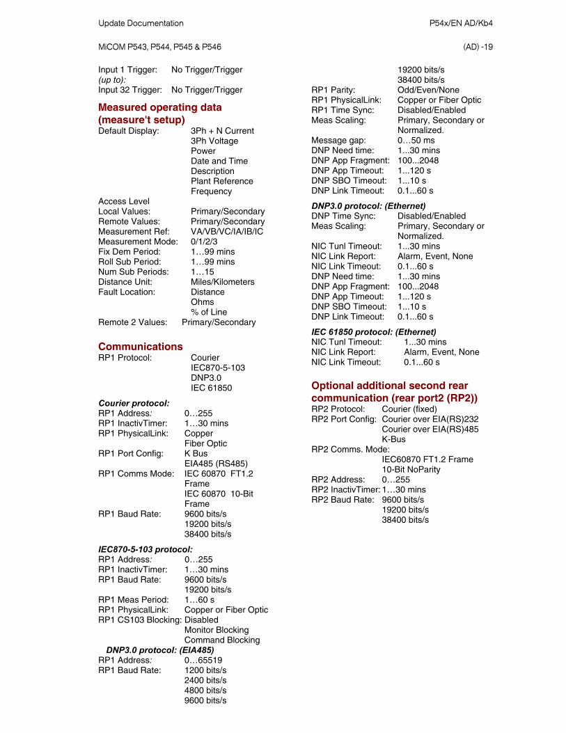
Input 1 Trigger: No Trigger/Trigger (up to): Input 32 Trigger: No Trigger/Trigger
Measured operating data (measure't setup) Default Display: 3Ph + N Current
3Ph Voltage Power Date and Time Description Plant Reference Frequency
Access Level Local Values: Primary/Secondary Remote Values: Primary/Secondary Measurement Ref: VA/VB/VC/IA/IB/IC Measurement Mode: 0/1/2/3 Fix Dem Period: 1…99 mins Roll Sub Period: 1…99 mins Num Sub Periods: 1…15 Distance Unit: Miles/Kilometers Fault Location: Distance
Ohms % of Line
Remote 2 Values: Primary/Secondary
Communications RP1 Protocol: Courier
IEC870-5-103 DNP3.0 IEC 61850
Courier protocol: RP1 Address: 0…255 RP1 InactivTimer: 1…30 mins RP1 PhysicalLink: Copper
Fiber Optic RP1 Port Config: K Bus
EIA485 (RS485) RP1 Comms Mode: IEC 60870 FT1.2
Frame IEC 60870 10-Bit Frame
RP1 Baud Rate: 9600 bits/s 19200 bits/s 38400 bits/s
IEC870-5-103 protocol: RP1 Address: 0…255 RP1 InactivTimer: 1…30 mins RP1 Baud Rate: 9600 bits/s
19200 bits/s RP1 Meas Period: 1…60 s RP1 PhysicalLink: Copper or Fiber Optic RP1 CS103 Blocking: Disabled
Monitor Blocking Command Blocking
DNP3.0 protocol: (EIA485) RP1 Address: 0…65519 RP1 Baud Rate: 1200 bits/s
2400 bits/s 4800 bits/s 9600 bits/s
19200 bits/s 38400 bits/s
RP1 Parity: Odd/Even/None RP1 PhysicalLink: Copper or Fiber Optic RP1 Time Sync: Disabled/Enabled Meas Scaling: Primary, Secondary or
Normalized. Message gap: 0…50 ms DNP Need time: 1...30 mins DNP App Fragment: 100...2048 DNP App Timeout: 1...120 s DNP SBO Timeout: 1...10 s DNP Link Timeout: 0.1...60 s
DNP3.0 protocol: (Ethernet) DNP Time Sync: Disabled/Enabled Meas Scaling: Primary, Secondary or
Normalized. NIC Tunl Timeout: 1...30 mins NIC Link Report: Alarm, Event, None NIC Link Timeout: 0.1...60 s DNP Need time: 1...30 mins DNP App Fragment: 100...2048 DNP App Timeout: 1...120 s DNP SBO Timeout: 1...10 s DNP Link Timeout: 0.1...60 s
IEC 61850 protocol: (Ethernet) NIC Tunl Timeout: 1...30 mins NIC Link Report: Alarm, Event, None NIC Link Timeout: 0.1...60 s
Optional additional second rear communication (rear port2 (RP2)) RP2 Protocol: Courier (fixed) RP2 Port Config: Courier over EIA(RS)232
Courier over EIA(RS)485 K-Bus
RP2 Comms. Mode: IEC60870 FT1.2 Frame 10-Bit NoParity
RP2 Address: 0…255 RP2 InactivTimer: 1…30 mins RP2 Baud Rate: 9600 bits/s
19200 bits/s 38400 bits/s

P54x/EN AD/Kb4-S Update Documentation
(AD) -20
MiCOM P543, P544, P545 & P546
Commission tests
Monitor Bit 1: (up to): Monitor Bit 8: Binary function link strings,
selecting which DDB signals have their status visible in the Commissioning menu, for test purposes
Test Mode: Disabled Test Mode Blocked Contacts
Test Pattern: Configuration of which
output contacts are to be energized when the contact test is applied.
Contact Test: No Operation, Apply Test, Remove Test
Test LEDs: No Operation Apply Test Test Auto-reclose: No Operation
Trip 3 Pole Trip Pole A Trip Pole B Trip Pole C
Static Test Mode: Disabled/Enabled Static Test: Disabled/Enabled Loopback Mode: Disabled/Internal/External IM64 TestPattern: Configuration of which
InterMiCOM64 commands are to be set high or low for a loopback test.
IM64 Test Mode: Disabled/Enabled
Circuit breaker condition monitoring (CB Monitor setup) P543and P545 CB monitor setup: Broken I^: 1.0…2.0 I^ Maintenance: Alarm Disabled/Enabled I^ Maintenance: 1…25000 I^ Lockout: Alarm Disabled/Enabled I^ Lockout: 1…25000 No. CB Ops Maint: Alarm Disabled/Enabled No. CB Ops Maint: 1…10000 No. CB Ops Lock: Alarm Disabled/Enabled No. CB Ops Lock: 1…10000 CB Time Maint: Alarm Disabled/Enabled CB Time Maint: 0.005…0.500 s CB Time Lockout: Alarm Disabled/Enabled CB Time Lockout: 0.005…0.500 s Fault Freq. Lock: Alarm Disabled/Enabled Fault Freq. Count: 1…9999 Fault Freq. Time: 0…9999 s
P544 and P546 CB monitor setup: CB1 Broken �^: 1…2 CB1 �^ Maintenance: Alarm Disabled/
Alarm Enabled CB1 �^ Maintenance: 1…25000 �n^ CB1 �^ Lockout: Alarm Disabled/
Alarm Enabled CB1 �^ Lockout: 1…25000 �n^ No. CB1 Ops. Maint.: Alarm Disabled/ Alarm Enabled No. CB1 Ops. Maint.: 1…10000 No. CB1 Ops. Lock: Alarm Disabled/
Alarm Enabled No. CB1 Ops. Lock: 1…10000 CB1 Time Maint.: Alarm Disabled/
Alarm Enabled CB1 Time Maint.: 0.005…0.5 s CB1 Time Lockout: Alarm Disabled/
Alarm Enabled CB1 Time Lockout: 0.005…0.5 s CB1 Fault Freq. Lock: Alarm Disabled/
Alarm Enabled CB1 Flt Freq. Count: 1…9999 CB1 Flt Freq. Time: 0…9999 s CB2 Broken �^: (up to) CB2 Flt Freq. Time: All settings selected from
the same ranges as per the first controlled circuit breaker, CB1.
Optocoupled binary inputs (opto config.) Global threshold: 24 - 27 V
30 - 34 V 48 - 54 V 110 - 125 V 220 - 250 V
Custom Opto Input 1: (up to): Opto Input #. (# = max. opto no. fitted): Custom options allow
independent thresholds to be set per opto, from the same range as above.
Filter Control: Binary function link string,
selecting which optos will have an extra 1/2 cycle noise filter, and which will not.
Characteristics: Standard 60% - 80% 50% - 70%

Update Documentation P54x/EN AD/Kb4 MiCOM P543, P544, P545 & P546
(AD) -21
Control inputs into PSL (ctrl. I/P config.) Hotkey Enabled: Binary function link
string, selecting which of the control inputs will be driven from Hotkeys.
Control Input 1: Latched/Pulsed (up to): Control Input 32: Latched/Pulsed Ctrl Command 1: (up to): Ctrl Command 32: ON/OFF
SET/RESET IN/OUT ENABLED/DISABLED
EIA(RS)232 Teleprotection (INTERMiCOM Comms.) Source Address: 0…10 Received Address: 0…10 Data Rate: 600 Baud
1200 Baud 2400 Baud 4800 Baud 9600 Baud 19200 Baud
Loopback Mode: Disabled/Internal/External Test Pattern: Configuration of which InterMiCOM signals are to be energized when the loopback test is applied.
INTERMiCOM conf. IM Msg Alarm Lvl: 0.1…100.0% IM1 Cmd Type: Disabled/Direct/Blocking,
Permissive (up to): IM8 Cmd Type: Disabled/Direct/Blocking,
Permissive IM1 FallBackMode: Default/Latched (up to): IM8 FallBackMode: Default/Latched IM1 DefaultValue: 0/1 (up to): IM8 DefaultValue: 0/1 IM1 FrameSyncTim: 1 ms…1.5 s (up to): IM8 FrameSyncTim: 1 ms…1.5 s
Function keys
Fn. Key Status 1: (up to): Fn. Key Status 10 Disable
Lock Unlock/Enable
Fn. Key 1 Mode: Toggled/Normal (up to): Fn. Key 10 Mode: Toggled/Normal Fn. Key 1 Label: (up to): Fn. Key 10 Label: User defined text string to describe the function of the particular function key
IED configurator Switch Conf. Bank: No Action/Switch Banks
IEC 61850 GOOSE GoEna: Disabled
Enabled Test Mode: Disabled/
Pass Through/ Forced
VOP Test Pattern: 0x00000000... 0xFFFFFFFF
Ignore Test Flag: No/Yes
Prot comms/IM64 Scheme Setup:2 Terminal/Dual Redundant/3
Terminal Address: 0-0, 1-A…20-A, 1-
B….20-B Address: 0-0, 1-A…20-A, 1-
B….20-B, 1-C…20-C
Comm Mode: Standard/IEEE C37.94 Baud Rate Ch 1: 56kbits/s or 64kbits/s Baud Rate Ch 2: 56kbits/s or 64kbits/s Clock Source Ch1: Internal
External Clock Source Ch2: Internal
External Ch1 N*64kbits/s: Auto, 1, 2, 3... 12 Ch2 N*64kbits/s: Auto, 1, 2, 3... 12 Comm Delay Tol: 0.001 s...0.00005 s Comm Fail Timer: 0.1 s...600 s Comm Fail Mode: Ch 1 Failure/
Ch 2 Failure/ Ch 1 or Ch 2 Fail/ Ch 1 and Ch 2 Fail
GPS Sync: GPS Disabled, GPS � Standard, GPS � Inhibit, GPS � Restrain
Char Mod Time: 0...30 s Char Mod Ex : Disabled
Enabled Char Mod Ex Time: 0... 30 s Prop Delay Equal: No operation/
Restore CDiff Re-Configuration: Three Ended/
Two Ended (R1&R2)/ Two Ended (L&R2)/ Two Ended (L&R1)
Channel Timeout: 0.1 s...10 s Alarm Level: 0%...100% Prop Delay Stats: Disabled
Enabled MaxCh 1 PropDelay: 1 m...50 ms MaxCh 2 PropDelay: 1 m...50 ms TxRx Delay Stats: Disabled
Enabled MaxCh1 Tx-RxTime: 1 m...50 ms MaxCh2 Tx-RxTime: 1 m...50 ms GPS Fail Timer: 0…9999 s

P54x/EN AD/Kb4-S Update Documentation
(AD) -22
MiCOM P543, P544, P545 & P546 GPS Trans Fail: Disabled
Enabled GPS Trans Count: 1…100 s GPS Trans Timer: 0…9999 s IM1 Cmd Type: Direct
Permissive IM1 FallBackMode: Default
Latching IMx(x=1 to 8) DefaultValue: 0 or 1 The IM1 – IM8 s setting are common to both Ch1 and Ch2 (i.e. if IM1 DefaultValue is set to 0, it will be 0 on Ch1 and on Ch2)
Control input user labels (Ctrl. I/P labels) Control Input 1: (up to): Control Input 32: User defined text string to describe the function of the particular control input
Settings in multiple groups Note: All settings here onwards apply for setting groups # = 1 to 4.
Protection functions
Line parameters GROUP # (for # = 1 to 4) Line Length (km): 0.30…1000.00 km Line Length (miles): 0.20…625.00 mi Line Impedance: 0.05…500.00/In � Line Angle: 20…90° Residual Comp: 0.00…10.00 Residual Angle: -180…90° Mutual Comp: Disabled/Enabled KZm Mutual Set: 0.00…10.00 KZm Mutual Angle: -180…90° Mutual cut-off (k): 0.0…2.0 Phase Sequence: Standard ABC
Reverse ACB CB Tripping Mode (per CB as appropriate):
3 Pole 1 and 3 Pole
Line Charging Y: 0.00…10.00 ms
Distance setup Setting Mode: Simple/Advanced
Phase distance Phase Chars.: Mho/Quadrilateral Quad Resistance: Common/Proportional Fault Resistance: 0.05…500.00/In � Zone 1 Ph Status: Disabled/Enabled Zone 1 Ph Reach: 10…1000% of line Zone 2 Ph Status: Disabled/Enabled Zone 2 Ph Reach: 10…1000% of line Zone 3 Ph Status: Disabled/Enabled Zone 3 Ph Reach: 10…1000% of line Zone 3 Ph Offset: Disabled/Enabled Z3Ph Rev Reach: 10…1000% of line Zone P Ph Status: Disabled/Enabled Zone P Ph Dir.: Forward/Reverse Zone P Ph Reach: 10…1000% of line Zone 4 Ph Status: Disabled/Enabled Zone 4 Ph Reach: 10…1000% of line
Ground distance Ground Chars.: Mho/Quadrilateral Quad Resistance: Common/Proportional Fault Resistance: 0.05…500.00/In � Zone1 Gnd Status: Disabled/Enabled Zone1 Gnd Reach: 10…1000% of line Zone2 Gnd Status: Disabled/Enabled Zone2 Gnd Reach: 10…1000% of line Zone3 Gnd Status: Disabled/Enabled Zone3 Gnd Reach: 10…1000% of line Zone3 Gnd Offset: Disabled/Enabled Z3Gnd Rev Reach: 10…1000% of line ZoneP Gnd Status: Disabled/Enabled ZoneP Gnd Direction: Forward/Reverse ZoneP Gnd Reach: 10…1000% of line Zone4 Gnd Status: Disabled/Enabled Zone4 Gnd Reach: 10…1000% of line Digital Filter: Standard
Special Applics CVT Filters: Disabled/Passive/Active

Update Documentation P54x/EN AD/Kb4 MiCOM P543, P544, P545 & P546
(AD) -23
SIR Setting: (for CVT): 5…60 Load Blinders: Disabled/Enabled Load/B Impedance: 0.10…500.00/In � Load/B Angle: 15…65° Load Blinder V<: 1.0…70.0 V (ph-g) Distance Polarizing: 0.2…5.0 Delta Status: Disabled/Enabled Delta Char Angle: 0°...90° Delta V Fwd: 1.0…30.0 V Delta V Rev: 0.5…30.0 V Delta I Fwd: 0.10…10.00 In Delta I Rev: 0.05…10.00 In
Distance elements - phase distance Z1 Ph. Reach: 0.05…500.00/In � Z1 Ph. Angle: 20…90° R1 Ph. Resistive: 0.05…500.00/In � Z1 Tilt Top Line: -30…30° Z1 Ph. Sensit. Iph>1: 0.050…2.000 In Z2 Ph. Reach: 0.05…500.00/In � Z2 Ph. Angle: 20…90° Z2 Ph Resistive: 0.05…500.00/In � Z2 Tilt Top Line: -30…30° Z2 Ph. Sensit. Iph>2: 0.050…2.000 In Z3 Ph. Reach: 0.05…500.00/In � Z3 Ph. Angle: 20…90° Z3' Ph Rev Reach: 0.05…500.00/In � R3 Ph Res. Fwd.: 0.05…500.00/In � R3' Ph Res. Rev.: 0.05…500.00/In � Z3 Tilt Top Line: -30…30° Z3 Ph. Sensit. Iph>3: 0.050…2.000 In ZP Ph. Reach: 0.05…500.00/In � ZP Ph. Angle: 20…90° ZP Ph Resistive: 0.05…500.00/In � ZP Tilt Top line: -30…30° ZP Ph. Sensit. Iph>P: 0.050…2.000In Z4 Ph. Reach: 0.05…500.00/In � Z4 Ph. Angle: 20…90° Z4 Ph Resistive: 0.05…500.00/In � Z4 Tilt Top line: -30…30° Z4 Ph. Sensit. Iph>4: 0.050…2.000 In
Ground distance parameters Z1 Gnd. Reach: 0.05…500.00/In � Z1 Gnd. Angle: 20…90° Z1 Dynamic Tilt: Disabled or Enabled Z1 Tilt top line: -30°...30° kZN1 Res. Comp.: 0.00…10.00 kZN1 Res. Angle: -180…90° kZm1 Mut. Comp.: 0.00…10.00 kZm1 Mut. Angle: -180…90° R1 Gnd. Resistive: 0.05…500.00/In � Z1 Sensit Ignd>1: 0.050…2.000 In Z2 Gnd. Reach: 0.05…500.00/In � Z2 Gnd. Angle: 20…90°
Z2 Dynamic Tilt: Disabled or Enabled Z2 Tilt top line: -30°...30° kZN2 Res. Comp.: 0.00…10.00 kZN2 Res. Angle: -180…90° kZm2 Mut. Comp: 0.00…10.00 kZm2 Mut. Angle: -180…90° R2 Gnd Resistive: 0.05…500.00/In � Z2 Sensit Ignd>2: 0.050…2.000 In Z3 Gnd. Reach: 0.05…500.00/In � Z3 Gnd. Angle: 20…90° Z3 Dynamic Tilt: Disabled or Enabled Z3 Tilt top line: -30°...30° Z3' Gnd Rev Rch: 0.05…500.00/In � kZN3 Res. Comp.: 0.00…10.00 kZN3 Res. Angle: -180…90° kZm3 Mut. Comp.: 0.00…10.00 kZm3 Mut. Angle: -180…90° R3 Gnd Res. Fwd: 0.05…500.00/In � R3 Gnd Res. Rev: 0.05…500.00/In � Z3 Sensit Ignd>3: 0.050…2.000 In ZP Ground Reach: 0.05…500.00/In � ZP Ground Angle: 20…90° ZP Dynamic Tilt: Disabled or Enabled ZP Tilt top line: -30°...30° kZNP Res. Comp.: 0.00…10.00 kZNP Res. Angle: -180…90° kZmP Mut. Comp.: 0.00…10.00 kZmP Mut. Angle: -180…90° RP Gnd Resistive: 0.05…500.00/In � ZP Sensit Ignd>P: 0.050…2.000 In Z4 Gnd. Reach: 0.05…500.00/In � Z4 Gnd. Angle: 20…90° Z4 Dynamic Tilt: Disabled or Enabled Z4 Tilt top line: -30°...30° kZN4 Res. Comp.: 0.00…10.00 kZN4 Res. Angle: -180…90° kZm4 Mut. Comp.: 0.00…10.00 kZm4 Mut. Angle: -180…90° R4 Gnd. Resistive: 0.05…500.00/In � Z4 Gnd Sensitivity: 0.050…2.000 In
Phase current differential protection
Phase Diff: Enabled or Disabled Phase Is1: 0.2 In...2 In Phase Is2: 1 In...30 In Phase k1: 30%...150% Phase k2: 30%...150% Phase Char: DT/IEC S Inverse/
IEC V Inverse/ IEC E inverse/ UK LT Inverse/ IEEE M Inverse/ IEEE V Inverse/ IEEE E Inverse/ US Inverse/ US ST Inverse
Phase Time Delay: 0 s...100 s Phase TMS: 0.025...1.2 Phase Time Dial: 0.01...100 PIT Time: 0 s...0.2 s Ph CT Corr'tion: 1...8

P54x/EN AD/Kb4-S Update Documentation
(AD) -24
MiCOM P543, P544, P545 & P546 Compensation: None/
Cap Charging/ Transformer
Susceptance: 1E-8*In...10*In Inrush Restraint: Restraint/Blocking/Disabled Ih(2) CrossBlock: Disabled/Enabled Ih(2) Multiplier: 1..20 Ih(2) %>: 5% ..50% Ih(5) CrossBlock: Disabled/Enabled Ih(5) Blocking: Disabled/Enabled Ih(5) %>: 5% ..100% Highset Status: Disabled/Enabled Id High Set: 4*ln...32*ln Vectorial Comp: Yy0 (0 deg)/
Yd1 (-30 deg)/ Yy2 (-60 deg)/ Yd3 (-90 deg)/ Yy4 (-120 deg)/ Yd5 (-150 deg)/ Yy6 (180 deg)/ Yd7 (+150 deg)/ Yy8 (+120 deg)/ Yd9 (+90 deg)/ Yy10 (+60 deg)/ Yd11 (+30 deg)/ Ydy0 (0 deg)/ Ydy6 (180 deg)
Phase Is1 CTS: 0.2*In...4*In PIT I Selection: Local or Remote
Scheme logic Basic scheme Zone 1 Tripping: Disabled/
Phase only/ Ground only/ Phase and Ground
tZ1 Ph. Delay: 0 s...10 s tZ1 Gnd. Delay: 0 s...10 s Zone 2 Tripping: Disabled/
Phase only/ Ground only/ Phase and Ground
tZ2 Ph. Delay: 0 s...10 s tZ2 Gnd. Delay: 0 s…10 s Zone 3 Tripping: Disabled/
Phase only/ Ground only/ Phase and Ground
tZ3 Ph. Delay: 0 s...10 s tZ2 Gnd. Delay: 0 s...10 s Zone P Tripping: Disabled/
Phase only/ Ground only/ Phase and Ground
tZP Ph. Delay: 0 s...10 s tZP Gnd. Delay: 0 s...10 s Zone 4 Tripping: Disabled/
Phase only/ Ground only/ Phase and Ground
tZ4 Ph. Delay: 0 s...10 s tZ4 Gnd. Delay: 0 s...10 s
Aided scheme 1 Aid 1 Selection: Disabled/
PUR/ PUR Unblocking/ POR/ POR/ Unblocking/ Blocking 1/ Blocking 2/ Prog Unblocking/ Programmable
Aid 1 Distance: Disabled/ Phase only/ Ground only/ Phase and Ground
Aid 1 Dist. Dly: 0 s...1 s Unblocking Delay: 0 s...0.1 s Aid 1 DEF: Disabled/Enabled Aid 1 DEF Dly: 0 s...1 s Aid 1 DEF Trip: 1/3 Pole Aid 1 Delta: 0.000… 1.000 s Aid1 Delta Dly: 0.000…1.000 s Aid1 DeltaTrip: 3 Pole
1 and 3 Pole tREV Guard: 0 s...0.15 s Unblocking Delay: 0 s...0.1 s Send on Trip Aided / Z1, Any Trip or None Weak Infeed: Disabled/
Echo/ Echo and Trip
WI Sngl Pole Trp: Disabled/Enabled WI V< Thresh: 10 V...70 V WI Trip Delay: 0 s...1 s Custom Send Mask: Bit 0 = Z1 Gnd/
Bit 1 = Z2 Gnd/ Bit 2 = Z4 Gnd/ Bit 3 = Z1 Ph/ Bit 4 = Z2 Ph/ Bit 5 = Z4 Ph/ Bit 6 = DEF Fwd/ Bit 7 = DEF Rev/ Bit
Custom Time PU: 0 s...1 s Custom Time DO: 0 s...1 s Aided scheme 2 (As per aided scheme 1) Trip on close SOTF Status: Disabled/
Enabled Pole Dead/ Enabled ExtPulse/ En Pdead + Pulse
SOTF Delay: 0.2s...1000s SOTF Tripping: Bit 0 = Zone 1/
Bit 1 = Zone 2/ Bit 2 = Zone 3/ Bit 3 = Zone P/ Bit 4 = Zone 4/ Bit 5=CNV
TOR Status: Disabled/Enabled

Update Documentation P54x/EN AD/Kb4 MiCOM P543, P544, P545 & P546
(AD) -25
TOR Tripping: Bit 0 = Zone 1/
Bit 1 = Zone 2/ Bit 2 = Zone 3/Bit 3 = Zone P/Bit 4 = Zone 4/Bit5=CNV
TOC Reset Delay: 0.1 s...2 s TOC Delay 0.05 s…0.2 s SOTF Pulse: 0.1 s...10 s Z1 extension Z1 Ext Scheme: Disabled/
Enabled/ En. on Ch1 Fail/ En. On Ch2 Fail/ En All Ch Fail/ En. anyCh Fail
Z1 Ext Ph: 100%...200% Z1 Ext Gnd: 100%...200%
Loss of load LOL Scheme: Disabled/
Enabled/ En. on Ch1 Fail/ En. On Ch2 Fail/ En All Ch Fail/ En. Any Ch Fail
LOL <I: 0.05 x In...1 x In LOL Window: 0.01 s 0.1 s Phase
Phase overcurrent (overcurrent) I>1 Status: Disabled
Enabled Enabled VTS Enabled Ch Fail En VTSorCh Fail En VTSandCh Fail
I>1 Function: DT IEC S Inverse IEC V Inverse IEC E Inverse UK LT Inverse IEEE M Inverse IEEE V Inverse IEEE E Inverse US Inverse US ST Inverse
I>1 Directional: Non-Directional Directional Fwd Directional Rev
I>1 Current Set: 0.08…4.00 In I>1 Time Delay: 0.00…100.00 s I>1 TMS: 0.025…1.200 I>1 Time Dial: 0.01…100.00 I>1 Reset Char: DT/Inverse I>1 tRESET: 0.00…100.00 s I>2 Status (up to): I>2 tRESET All settings and
options chosen from the same ranges as per the first stage overcurrent, I>1.
I>3 Status: Disabled Enabled Enabled VTS Enabled Ch Fail En VTSorCh Fail En VTSandCh Fail
I>3 Directional: Non-Directional Directional Fwd Directional Rev
I>3 Current Set: 0.08…32.00 In I>3 Time Delay: 0.00…100.00 s I>4 Status (up to): I>4 Time Delay All settings and
options chosen from the same ranges as per the third stage overcurrent, I>3.
I> Char Angle: -95…95° I> Blocking: Binary function link
string, selecting which overcurrent elements (stages 1 to 4) will be blocked if VTS detection of fuse failure occurs.
Negative sequence overcurrent (neg seq O/C) I2>1 Status: Enabled/Disabled I2>1 Function: Disabled
DT IEC S Inverse IEC V Inverse IEC E Inverse UK LT Inverse IEEE M Inverse IEEE V Inverse IEEE E Inverse US Inverse US ST Inverse
I2>1 Direction: Non-Directional Directional Fwd irectional Rev
I2>1 Current Set: 0.08…4.00 In I2>1 Time Delay: 0.00…100.00 s I2>1 TMS: 0.025…1.200 I2>1 Time Dial: 0.01…100.00 I2>1 Reset Char.: DT/Inverse I2>1 tRESET: 0.00…100.00 s I2>2 Status (up to): I2>2 tRESET All settings and options
chosen from the same ranges as per the first stage overcurrent, I2>1.
I2>3 Status: Disabled Enabled

P54x/EN AD/Kb4-S Update Documentation
(AD) -26
MiCOM P543, P544, P545 & P546 I2>3 Direction: Non-Directional
Directional Fwd Directional Rev
I2>3 Current Set: 0.08…32.00 In I2>3 Time Delay: 0.00…100.00 s I2>4 Status (up to): I2>4 Time Delay All settings and options
chosen from the same ranges as per the third stage overcurrent, I2>3.
I2> VTS Blocking: Binary function link string, selecting which Neg. Seq. O/C elements (stages 1 to 4) will be blocked if VTS detection of fuse failure occurs
I2> Char Angle: -95…95o I2> V2pol Set: 0.5…25.0
(100 – 110 V) Broken conductor Broken Conductor: Disabled/Enabled I2/I1 Setting: 0.20…1.00 I2/I1 Time Delay: 0.0…100.0 s
Ground overcurrent (earth fault) IN>1 Status: Disabled
Enabled Enabled VTS Enabled Ch Fail En VTSorCh Fail En VTSandCh Fail
IN>1 Function: DT IEC S Inverse IEC V Inverse IEC E Inverse UK LT Inverse IEEE M Inverse IEEE V Inverse IEEE E Inverse US Inverse US ST Inverse IDG
IN>1 Directional: Non-Directional Directional Fwd Directional Rev
IN>1 Current Set: 0.08…4.00 In IN>1 IDG Is: 1...4 IN>1 IDG Time: 1…2 IN>1 Time Delay: 0.00…100.00 s IN>1 TMS: 0.025…1.200 IN>1 Time Dial: 0.01…100.00 IN>1 Reset Char: DT/Inverse IN>1 tRESET: 0.00…100.00 s IN>2 Status (up to): IN>2 tRESET All settings and
options chosen from the same ranges as per the first stage
ground overcurrent, IN>1.
IN>3 Status: Disabled Enabled Enabled VTS Enabled Ch Fail En VTSorCh Fail En VTSandCh Fail
IN>3 Directional: Non-Directional Directional Fwd Directional Rev
IN>3 Current Set: 0.08…32.00 In IN>3 Time Delay: 0.00…100.00 s IN>4 Status (up to): IN>4 Time Delay All settings and
options chosen from the same ranges as per the third stage ground overcurrent, IN>3.
IN> Blocking: Binary function link string, selecting which ground overcurrent elements (stages 1 to 4) will be blocked if VTS detection of fuse failure occurs.
IN> DIRECTIONAL IN> Char Angle: -95…95° IN> Polarization: Zero Sequence Neg Sequence IN> VNpol Set: 0.5…40.0 V IN> V2pol Set: 0.5…25.0 V IN> I2pol Set: 0.02…1.00 In
Directional aided schemes - DEF settings DEF Status: Disabled/Enabled DEF Polarizing: Zero Sequence (virtual
current pol) Neg Sequence
DEF Char Angle: -95…95° DEF VNpol Set: 0.5…40.0 V DEF V2pol Set: 0.5…25.0 V DEF FWD Set: 0.08…1.00 In DEF REV Set: 0.04…1.00 In Sensitive Earth Fault protection/ Restricted Earth Fult protection SEF/REF Options: SEF Enabled
Wattmetric SEF HI Z REF
ISEF>1 Function: IDMT Curve Type Disabled DT IEC S Inverse IEC V Inverse IEC E Inverse UK LT Inverse IEEE M Inverse IEEE V Inverse

Update Documentation P54x/EN AD/Kb4 MiCOM P543, P544, P545 & P546
(AD) -27
IEEE E Inverse US Inverse US ST Inverse IDG
ISEF>1 Directional: Non-Directional Directional Fwd Directional Rev
ISEF>1 Current Set: 0.005…0.1 InSEF
ISEF>1 IDG Is: 1...4 ISEF>1 IDG Time: 1…2 s ISEF>1 Time Delay: 0 s…..200 s ISEF>1 TMS: 0.025…1.2 ISEF>1 Time Dial: 0.01…100 ISEF>1 Reset Char: DT/Inverse ISEF>1 tRESET: 0 s-100 s ISEF>2 as ISEF>1 ISEF>3 Status: Disabled
Enabled ISEF>3 Directional: Non-Directional
Directional Fwd Directional Rev
ISEF>3 Current Set: 0.005…0.8 InSEF ISEF>3 Time Delay: 0 s…200 s ISEF>3 Intertrip: Enabled/Disabled ISEF>4 as ISEF>3 ISEFN> Blocking Bit 0 VTS Blks ISEF>1 Bit 1 VTS Blks ISEF>2 Bit 2 VTS Blks ISEF>3 Bit 3 VTS Blks ISEF>4 Bit 4 A/R Blks ISEF>3 Bit 5 A/R Blks ISEF>4 Bit 6 Not Used Bit 7 Not Used ISEF> Directional ISEF> Char Angle: -95°…95° deg ISEF> VNpol Set: 0.5…80 V Wattmetric SEF PN> Setting: 0...20 InSEF W REF IREF>Is: 0.05 In .. 1.0 In
Neutral voltage displacement (residual O/V NVD) VN>1 Function: Disabled
DT IDMT
VN>1 Voltage Set: 1…80 V VN>1 Time Delay: 0.00…100.00 s VN>1 TMS: 0.5…100.0 VN>1 tReset: 0.00…100.00 s VN>2 Status: Disabled/Enabled VN>2 Voltage Set: 1…80 V VN>2 Time Delay: 0.00…100.00 s
Thermal overload Characteristic: Disabled
Single Dual
Thermal Trip: 0.08…4.00 In Thermal Alarm: 50…100% Time Constant 1: 1…200 mins Time Constant 2: 1…200 mins
Power swing/out of step (power swing) Power Swing: Blocking
Indication PSB Reset Delay: 0.05…2.00 s Zone 1 Ph PSB: Blocking/Allow Trip (up to): Zone 4 Ph PSB: Blocking/Allow Trip Zone 1 Gnd PSB: Blocking/Allow Trip (up to): Zone 4 Gnd PSB: Blocking/Allow Trip PSB Unblocking: Disabled/Enabled PSB Unblock Delay: 0.1…10.0 s PSB Reset Delay: 0.5…2.0 s
Out of step OST (Out of Step Tripping) mode:
Disabled Predictive and OST Trip OST Trip Predictive OST
Z5 Fwd Reach: 0.1…500.00/In � Z6 Fwd Reach: 0.1…500.00/In � Z5’ Rev Reach: 0.1…500.00/In � Z6’ Rev Reach: 0.1…500.00/In � R5 Res. Fwd: 0.1…200.00/In � R6 Res. Fwd: 0.1…200.00/In � R5’ Res. Rev: -0.1…-200.00/In � R6’ Res. Rev: -0.1…-200.00/In � Blinder Angle: 20…90°
Delta t Time Setting: 0.02 s…1 s Tost Time Delay Setting: 0 s…1 s
Undervoltage protection V< Measur't Mode: V<1 & V<2 Ph-Ph,
V<1 & V<2 Ph-N, V<1Ph-Ph V<2Ph-N, V<1Ph-N V<2Ph-Ph
V< Operate Mode: V<1 & V<2 Any Ph V<1 & V<2 3Phase V<1AnyPh V<2 3Ph V<1 3Ph V<2AnyPh
V<1 Function: Disabled DT IDMT
V<1 Voltage Set: 10…120 V V<1 Time Delay: 0.00…100.00 s V<1 TMS: 0.5… 100.0 V<1 Poledead Inh: Disabled/Enabled V<2 Status: Disabled/Enabled V<2 Voltage Set: 10…120 V

P54x/EN AD/Kb4-S Update Documentation
(AD) -28
MiCOM P543, P544, P545 & P546 V<2 Time Delay: 0.00…100.00 s V<2 Poledead Inh: Disabled/Enabled
Overvoltage protection V> Measur't Mode: V>1 & V>2 Ph-Ph,
V>1 & V>2 Ph-N, V>1Ph-Ph V>2Ph-N, V>1Ph-N V>2Ph-Ph
V> Operate Mode: V>1 & V>2 Any Ph V>1 & V>2 3Phase V>1AnyPh V>2 3Ph V>1 3Ph V>2AnyPh
V>1 Function: Disabled DT IDMT
V>1 Voltage Set: 60…185 V V>1 Time Delay: 0.00…100.00 s V>1 TMS: 0.5…100.0 V>2 Status: Disabled/Enabled V>2 Voltage Set: 60…185 V V>2 Time Delay: 0.00…100.00 s V1>1 Cmp Funct: Disabled
DT IDMT
V1>1 Cmp Vlt Set: 60…110 V V1>1 Cmp Tim Dly: 0.00…100.00 s V1>1 CmpTMS: 0.5…100.0 V1>2 Cmp Status: Disabled/Enabled V1>2 Vlt Set: 60… 110 V V1>2 CmpTim Dly: 0.00…100.00 s
Underfrequency protection F<1 Status: Disabled/Enabled F<1 Setting: 45.00…65.00 Hz F<1 Time Delay: 0.00…100.00 s F<2 Status (up to): F<4 Time Delay All settings and
options chosen from the same ranges as per the 1st stage
F< Function Link: Binary function link
string, selecting which frequency elements (stages 1 to 4) will be blocked by the pole-dead logic
Overfrequency protection
F>1 Status: Disabled/Enabled F>1 Setting: 45.00…65.00 Hz F>1 Time Delay: 0.00…100.00 s F>2 Status (up to): F>2 Time Delay All settings and options chosen from the same ranges as per the 1st stage
Rate-of-change of frequency protection (df/dt protection) df/dt Avg. Cycles: 6…12 df/dt>1 Status: Disabled/Enabled df/dt>1 Setting: 0.1…10.0 Hz df/dt>1 Dir’n.: Negative/Positive/Both df/dt>1 Time: 0.00…100.00 s df/dt>2 Status: (up to): df/dt>4 Time All settings and options chosen from the same ranges as per the 1st stage.
Circuit breaker fail CB Fail 1 Status: Disabled/Enabled CB Fail 1 Timer: 0.00…10.00 s CB Fail 2 Status: Disabled/Enabled CB Fail 2 Timer: 0.00…10.00 s Volt Prot Reset: I< Only
CB Open & I< Prot Reset & I<
Ext Prot Reset: I< Only CB Open & I< Prot Reset & I<
WI Prot Reset: Disabled/Enabled Undercurrent
I< Current Set: 0.02…3.20 In ISEF< Current Set: 0.001…0.8 InSEF
Poledead V< : 10 …40 V
Supervision VT Supervision VTS Mode: Measured + MCB,
Measured only or MCB only
VTS Status: Disabled/ Blocking/ Indication
VTS Reset Mode: Manual/Auto VTS Time Delay: 1 s...10 s VTS I> Inhibit: 0.08....32 x In VTS I2> Inhibit: 0.05...0.5 x In Inrush Detection I> 2nd Harmonic: 10%...100% Weak Infeed Blk WI Inhibit: Disabled/Enabled I0/I2 Setting: 2...3 CTS Mode: Disabled,
Standard, I Diff, Idiff + Standard
CTS Status: Restrain, Indication, CTS Reset Mode: Manual or Auto CTS Time Delay: 0...10 s CTS VN< Inhibit: 0.5 V...22 V CTS i1>: 0.05*In...4.0*In CTS i2/i1>: 0.05...1 CTS i2/i1>>: 0.05...1

Update Documentation P54x/EN AD/Kb4 MiCOM P543, P544, P545 & P546
(AD) -29
Systems check Bus-Line Synchronism and Voltage Checks (System Checks) P543 and P545 system checks: Voltage Monitors Live Voltage: 1.0…132.0 V Dead Voltage: 1.0…132.0 V Synchrocheck (Check Synch) CS1 Status: Disabled/Enabled CS1 Phase Angle: 0…90° CS1 Slip Control: None Timer Frequency Both CS1 Slip Freq: 0.02…1.00 Hz CS1 Slip Timer: 0.0…99.0 s CS2 Status (up to): CS2 Slip Timer All settings and options chosen from the same ranges as per the first stage CS1 element. CS Undervoltage: 10.0…132.0 V CS Overvoltage: 60.0…185.0 V CS Diff Voltage: 1.0…132.0 V CS Voltage Block: None
Undervoltage Overvoltage Differentia UV & OV UV & DiffV OV & DiffV UV, OV & DiffV
System Split SS Status: Disabled/Enabled SS Phase Angle: 90…175° SS Under V Block: Disabled/Enabled SS Undervoltage: 10.0…132.0 V SS Timer: 0.0…99.0 s
P544 and P546 system checks: Voltage Monitors Live Line: 5…132 V Dead Line: 5…132 V Live Bus 1: 5…132 V Dead Bus 1: 5…132 V Live Bus 2: 5…132 V Dead Bus 2: 5…132 V CS UV: 5…120 V CS OV: 60…200 V Sys Checks CB1: Enabled/Disabled CB1 CS Volt. Blk: V< , V> , Vdiff.> ,
V< and V>, V< and Vdiff> , V> and Vdiff> , V< V> and Vdiff> , None
CB1 CS1: Status Enabled or Disabled CB1 CS1 Angle: 0…90° CB1 CS1 Vdiff: 1…120 V CB1 CS1 SlipCtrl: Enabled/Disabled CB1 CS1 SlipFreq: 5 mHz…2 Hz CB1 CS2: Status Enabled/Disabled
CB1 CS2 Angle: 0…90° CB1 CS2 Vdiff: 1…120 V CB1 CS2 SlipCtrl: Enabled/Disabled CB1 CS2 SlipFreq: 5 mHz…2 Hz CB1 CS2 Adaptive: Enabled/Disabled CB1 Cl Time: 10.0 ms…0.5 s Sys Checks CB2: (up to): CB2 Cl Time: All settings and options
chosen from the same ranges as per the first controlled circuit breaker, CB1.
Manual System Checks Num CBs: CB1 only,
CB2 only, CB1 & CB2.
CB1M SC required: Enabled/Disabled CB1M SC CS1: Enabled/Disabled CB1M SC CS2: Enabled/Disabled CB1M SC DLLB: Enabled/Disabled CB1M SC LLDB: Enabled/Disabled CB1M SC DLDB: Enabled/Disabled CB2M SC required: (up to): CB2M SC DLDB: All settings and
options chosen from the same ranges as per the first controlled circuit breaker, CB1.
Auto-reclose P543 and P545 auto-reclose: Single Pole Shot: 1/2/3/4 Three Pole Shot: 1/2/3/4 1 Pole Dead Time: 0.05…5.00 s Dead Time 1: 0.05…100.00 s Dead Time 2: 1…1800 s Dead Time 3: 1…3600 s Dead Time 4: 1…3600 s CB Healthy Time: 1…3600 s Reclaim Time: 1…600 s AR Inhibit Time: 0.01…600.00 s Check Sync Time: 0.01…9999.00 s Z2T AR: (up to): Z4T AR: No Action
Initiate AR Block AR
All time-delayed distance zones can be independently set not to act upon AR logic, to initiate a cycle, or to block.
DEF Aided AR: Initiate AR Block AR
TOR: Initiate AR Block AR
I>1 AR: (up to): I>4 AR: No Action
Initiate AR Block AR

P54x/EN AD/Kb4-S Update Documentation
(AD) -30
MiCOM P543, P544, P545 & P546 All overcurrent stages
can be independently set not to act upon AR logic, to initiate a cycle, or to block.
IN>1 AR: (up to): IN>4 AR: No Action
Initiate AR Block AR
All ground/earth overcurrent stages can be independently set not to act upon AR logic, to initiate a cycle, or to block.
ISEF>1 AR: (up to): ISEF>4 AR: No Action Initiate AR Block AR All ground/earth
overcurrent stages can be independently set not to act upon AR logic, to initiate a cycle, or to block.
Mult Phase AR: Allow Autoclose BAR 2 and 3Ph BAR 3 Phase Dead Time Start: Protection Op Protection Reset Discrim Time: 0.10…5.00 s System Checks CheckSync1 Close: Disabled/Enabled CheckSync2 Close: Disabled/Enabled LiveLine/DeadBus: Disabled/Enabled DeadLine/LiveBus: Disabled/Enabled DeadLine/DeadBus: Disabled/Enabled CS AR Immediate: Disabled/Enabled SysChk on Shot 1: Disabled/Enabled P544 and P546 Auto-reclose: Num CBs: CB1 only,
CB2 only, Both CB1 & CB2
Lead/Foll AR Mode: L1P F1P, L1P F3P, L3P F3P, L1/3P F1/3P, L1/3P F3P, Opto
AR Mode: AR 1P, AR 1/3P, AR 3P,AR Opto
Leader Select By: Leader by Menu, Leader by Opto, Leader by Ctrl
Select Leader: Sel Leader CB1, Sel Leader CB2
BF if LFail Cls: Enabled/Disabled Dynamic F/L: Enabled/Disabled AR Shots: 1…4
Multi Phase AR: Allow Autoclose, BAR 2 and 3 ph, BAR 3 phase
Discrim Time: 20 ms…5 s CB IS Time: 5…200 s CB IS MemoryTime: 10 ms…1 s DT Start by Prot: Protection Reset,
Protection Op, Disabled
3PDTStart WhenLD: Enabled/Disabled DTStart by CB Op: Enabled/Disabled Dead Line Time: 1…9999 s SP AR Dead Time: 0…10 s 3P AR DT Shot 1: 10 ms…300 s 3P AR DT Shot 2: 1…9999 s 3P AR DT Shot 3: 1…9999 s 3P AR DT Shot 4: 1…9999 s Follower Time: 100 ms…300 s SPAR ReclaimTime: 1…600 s 3PAR ReclaimTime: 1…600s AR CBHealthy Time: 0.01…9999 s AR CheckSync Time: 0.01…9999 s Z1 AR: Initiate AR Block AR Diff AR: Initiate AR Block AR Dist. Aided AR: Initiate AR Block AR Z2T AR: (up to): Z4T AR: No Action Initiate AR Block AR All time-delayed
distance zones can be independently set not to act upon AR logic, to initiate a cycle, or to block.
DEF Aided AR: Initiate AR Block AR Dir. Comp AR: Initiate AR Block AR TOR: Initiate AR Block AR I>1 AR: (up to): I>4 AR: No Action Initiate AR Block AR All overcurrent stages
can be independently set not to act upon AR logic, to initiate a cycle, or to block.
IN>1 AR: (up to): IN>4 AR: No Action Initiate AR Block AR All ground/earth
overcurrent stages can be independently set not to act upon AR

Update Documentation P54x/EN AD/Kb4 MiCOM P543, P544, P545 & P546
(AD) -31
logic, to initiate a cycle, or to block.
ISEF>1 AR: (up to): ISEF>4 AR: No Action
Initiate AR Block AR
All ground/earth overcurrent stages can be independently set not to act upon AR logic, to initiate a cycle, or to block.
Auto-reclose system checks CB1L SC all: Enabled/Disabled CB1L SC Shot 1: Enabled/Disabled CB1L SC ClsNoDly: Enabled/Disabled CB1L SC CS1: Enabled/Disabled CB1L SC CS2: Enabled/Disabled CB1L SC DLLB: Enabled/Disabled CB1L SC LLDB: Enabled/Disabled CB1L SC DLDB: Enabled/Disabled CB2L SC all: Enabled/Disabled CB2L SC Shot 1: Enabled/Disabled CB2L SC ClsNoDly: Enabled/Disabled CB2L SC CS1: Enabled/Disabled CB2L SC CS2: Enabled/Disabled CB2L SC DLLB: Enabled/Disabled CB2L SC LLDB: Enabled/Disabled CB2L SC DLDB: Enabled/Disabled CB1F SC all: Enabled/Disabled CB1F SC Shot 1: Enabled/Disabled CB1F SC CS1: Enabled/Disabled CB1F SC CS2: Enabled/Disabled CB1F SC DLLB: Enabled/Disabled CB1F SC LLDB: Enabled/Disabled CB1F SC DLDB: Enabled/Disabled CB2F SC all: Enabled/Disabled CB2F SC Shot 1: Enabled/Disabled CB2F SC CS1: Enabled/Disabled CB2F SC CS2: Enabled/Disabled CB2F SC DLLB: Enabled/Disabled CB2F SC LLDB: Enabled/Disabled CB2F SC DLDB: Enabled/Disabled
Opto input labels Opto Input 1: (up to): Opto Input 32: User defined text string to describe the
function of the particular opto input.
Output labels Relay 1: (up to): Relay 32: User defined text string to describe the
function of the particular relay output contact.
Measurements list
Measurements 1 I� Magnitude I� Phase Angle
Per phase (� = A, B, C) current measurements IN derived Mag IN derived Angle ISEF Mag ISEF Angle I1 Magnitude I2 Magnitude I0 Magnitude I� RMS Per phase (� = A, B, C) RMS current measurements IN RMS V�-� Magnitude V�-� Phase Angle V� Magnitude V� Phase Angle All phase-phase and phase-neutral voltages (� = A, B, C). V1 Magnitude V2 Magnitude V0 Magnitude V� RMS V�-� RMS All phase-phase and phase-neutral voltages (� = A, B, C). Frequency (CB1) CS Volt Mag (CB1) CS Volt Ang (CB1) Bus-Line Ang (CB1) CS Slip Freq IM Magnitude IM Phase Angle I1 Magnitude I1 Phase Angle I2 Magnitude I2 Phase Angle I0 Magnitude I0 Phase Angle V1 Magnitude V1 Phase Angle V2 Magnitude V2 Phase Angle V0 Magnitude V0 Phase Angle CB2 CS Volt Mag (P544 and P546 only) CB2 CS Volt Ang (P544 and P546 only) CB2 Bus-Line Ang (P544 and P546 only) CB2 CS Slip Freq (P544 and P546 only) V1 Rem Magnitude V1 Rem Phase Ang IA CT1 Magnitude (P544 and P546 only) IA CT1 Phase Ang (P544 and P546 only) IB CT1 Magnitude (P544 and P546 only) IB CT1 Phase Ang (P544 and P546 only) IC CT1 Magnitude (P544 and P546 only) IC CT1 Phase Ang (P544 and P546 only) IA CT2 Magnitude (P544 and P546 only) IA CT2 Phase Ang (P544 and P546 only) IB CT2 Magnitude (P544 and P546 only) IB CT2 Phase Ang (P544 and P546 only) IC CT2 Magnitude (P544 and P546 only) IC CT2 Phase Ang (P544 and P546 only)

P54x/EN AD/Kb4-S Update Documentation
(AD) -32
MiCOM P543, P544, P545 & P546 Measurements 2 � Phase Watts � Phase VArs � Phase VA All phase segregated power measurements, real, reactive and apparent (� = A, B, C). 3 Phase Watts 3 Phase VArs 3 Phase VA Zero Seq Power 3Ph Power Factor �Ph Power Factor Independent power factor measurements for all three phases (� = A, B, C). 3Ph WHours Fwd 3Ph WHours Rev 3Ph VArHours Fwd 3Ph VArHours Rev 3Ph W Fix Demand 3Ph VArs Fix Dem I� Fixed Demand Maximum demand currents measured on a per phase basis (� = A, B, C). 3Ph W Roll Dem 3Ph VArs Roll Dem I� Roll Demand Maximum demand currents measured on a per phase basis (� = A, B, C). 3Ph W Peak Dem 3Ph VAr Peak Dem I� Peak Demand Maximum demand currents measured on a per phase basis (� = A, B, C). Thermal State
Measurements 3 IA Local IA Angle Local IB Local IB Angle Local IC Local IC Angle Local IA remote 1 IA Ang remote 1 IB remote 1 IB Ang remote 1 IC remote 1 IC Ang remote 1 IA remote 2 IA Ang remote 2 IB remote 2 IB Ang remote 2 IC remote 2 IC Ang remote 2 IA Differential IB Differential IC Differential IA Bias IB Bias IC Bias
Measurements 4 Ch 1 Prop Delay Ch 2 Prop Delay Ch1 Rx Prop Delay Ch1 Tx Prop Delay Ch2 Rx Prop Delay Ch2 Tx Prop Delay Channel 1 Status Channel 2 Status Channel Status: Bit 0= Rx Bit 1= Tx Bit 2= Local GPS Bit 3= Remote GPS Bit 4= Mux Clk F Error Bit 5= Signal Lost Bit 6= Path Yellow Bit 7= Mismatch RxN Bit 8= Timeout Bit 9= Message Level Bit 10= Passthrough Bit 11= Hardware B to J model Bit 12= Max Prop Delay Bit 13= Max Tx-Rx Time Binary function link strings denoting channel errors, and when self-healing has been initiated in 3-terminal applications. IM64 Rx Status Statistics Last Reset on Date/Time Ch1 No. Vald Mess Ch1 No. Err Mess Ch1 No. Errored s Ch1 No. Sev Err s Ch1 No. Dgraded m Ch2 No. Vald Mess Ch2 No. Err Mess Ch2 No. Errored s Ch2 No. Sev Err s Ch2 No. Dgraded m Max Ch 1 Prop Delay Max Ch 2 Prop Delay Max Ch1 TxRx Time Max Ch2 TxRx Time Clear Statistics
Circuit breaker monitoring statistics CB Operations CB � Operations Circuit breaker operation counters on a per phase basis (� = A, B, C). Total I� Broken Cumulative breaker interruption duty on a per phase basis (� = A, B, C). CB Operate Time For a second circuit breaker (P544 and P546 only) CB2 Operations CB2 � Operations Circuit breaker operation counters on a per phase basis (� = A, B, C).

Update Documentation P54x/EN AD/Kb4 MiCOM P543, P544, P545 & P546
(AD) -33
CB2 I� Broken Cumulative breaker interruption duty on a per phase basis (� = A, B, C). CB 2Operate Time
Fault record proforma The following data is recorded for any relevant elements that operated during a fault, and can be viewed in each fault record. Time & Date Model Number: Address: Event Type: Fault record Event Value Faulted Phase: Binary data strings for fast polling of which phase elements started or tripped for the fault recorded. Start Elements Trip Elements Binary data strings for fast polling of which protection elements started or tripped for the fault recorded. Fault Alarms Binary data strings for fast polling of alarms for the fault recorded. Fault Time Active Group: 1/2/3/4 System Frequency: Hz Fault Duration: s CB Operate Time: s Relay Trip Time: s Fault Location: km/miles/�/% I �Pre Flt I� Angle Pre Flt Per phase record of the current magnitudes and phase angles stored before the fault inception. IN Prefault Mag IN Prefault Ang IM Prefault Mag IM Prefault Ang V� Prefault Mag V� Prefault Ang Per phase record of the voltage magnitudes and phase angles stored before the fault inception. VN Prefault Mag VN Prefault Ang I� Fault Mag I� Fault Ang Per phase record of the current magnitudes and phase angles during the fault. IN Fault Mag IN Fault Ang IM Fault Mag IM Fault Ang V� Fault Mag V� Fault Ang Per phase record of the voltage magnitudes and phase angles during the fault. VN Fault Mag
VN Fault Ang IA local IB local IC local IA remote 1 IB remote 1 IC remote 1 IA remote 2 IB remote 2 IC remote 2 IA Differential IB Differential IC Differential IA Bias IB Bias IC Bias Ch1 Prop Delay Ch 2 Prop Delay Ch1 Rx Prop Delay Ch1 Tx Prop Delay Ch2 Rx Prop Delay Ch2 Tx Prop Delay V1 Rem Magnitude V1 Rem Phase Ang Fault IA Local Fault IB Local Fault IC Local Fault IA rem 1 Fault IB rem 1 Fault IC rem 1 Fault IA rem 2 Fault IB rem 2 Fault IC rem 2 Fault IA Diff Fault IB Diff Fault IC Diff Fault IA Bias Fault IB Bias Fault IC Bias

P54x/EN AD/Kb4-S Update Documentation
(AD) -34
MiCOM P543, P544, P545 & P546
SETTINGS (P54x/EN ST/Ba4)
1.1 Relay Settings Configuration The relay is a multi-function device that supports numerous different protection, control and communication features. In order to simplify the setting of the relay, there is a configuration settings column which can be used to enable or disable many of the functions of the relay. The settings associated with any function that is disabled are made invisible in the menu. To disable a function change the relevant cell in the Configuration column from Enabled to Disabled.
The configuration column controls which of the four protection settings groups is selected as active through the Active settings cell. A protection setting group can also be disabled in the configuration column, provided it is not the present active group. Similarly, a disabled setting group cannot be set as the active group.
The column also allows all of the setting values in one group of protection settings to be copied to another group.
To do this firstly set the Copy from cell to the protection setting group to be copied, and then set the copy to cell to the protection group where the copy is to be placed. The copied settings are initially placed in the temporary scratchpad, and will only be used by the relay following confirmation.
Menu text Default setting Available settings
Restore Defaults No Operation
No Operation All Settings Setting Group 1 Setting Group 2 Setting Group 3 Setting Group 4
Setting to restore a setting group to factory default settings. To restore the default values to the settings in any Group settings, set the ‘restore defaults’ cell to the relevant Group number. Alternatively it is possible to set the ‘restore defaults’ cell to ‘all settings’ to restore the default values to all of the IED’s settings, not just the Group settings. The default settings will initially be placed in the scratchpad and will only be used by the relay after they have been confirmed by the user. Note: Restoring defaults to all settings includes the rear communication port settings, which may result in communication via the rear port being disrupted if the new (default) settings do not match those of the master station.
Setting Group Select via Menu Select via Menu Select via Optos
Allows setting group changes to be initiated via Opto Input or via Menu.
Active Settings Group 1 Group 1, Group 2, Group 3, Group 4
Selects the active setting group.
Save Changes No Operation No Operation, Save, Abort
Saves all relay settings.
Copy from Group 1 Group 1, 2, 3 or 4
Allows displayed settings to be copied from a selected setting group.
Copy to No Operation No Operation Group 1, 2, 3 or 4
Allows displayed settings to be copied to a selected setting group (ready to paste).
Setting Group 1 Enabled Enabled or Disabled
If the setting group is disabled from the configuration, then all associated settings and signals are hidden, with the exception of this setting (paste).
Setting Group 2 (as above) Disabled Enabled or Disabled
Setting Group 3 (as above) Disabled Enabled or Disabled
Setting Group 4 (as above) Disabled Enabled or Disabled

Update Documentation P54x/EN AD/Kb4 MiCOM P543, P544, P545 & P546
(AD) -35
Menu text Default setting Available settings
Distance Enabled Enabled or Disabled
Only in models with Distance option. To enable (activate) or disable (turn off) the Distance Protection: ANSI 21P/21G.
Directional E/F Enabled Enabled or Disabled
Only in models with Distance option. To enable (activate) or disable (turn off) the Directional Earth Fault (DEF) Protection used in a pilot aided scheme: ANSI 67N. This protection is independent from back up Earth fault protection described below.
Phase Diff Enabled Enabled or Disabled
To enable (activate) or disable (turn off) the Differential Protection. To get the differential protection fully active, it is necessary also to enable the differential protection in the group. Phase Diff setting and InterMiCOM64 Fiber setting are mutually exclusive as with Phase Diff enabled, the digital message exchanged has the structure of the differential message (i.e. currents are sent to the remote end, etc) and with InterMiCOM64 Fiber the digital message exchanged has the structure and properties of the InterMiCOM64 Fiber.
Overcurrent Enabled Enabled or Disabled
To enable (activate) or disable (turn off) the Phase Overcurrent Protection function. I> stages: ANSI 50/51/67P.
Neg. Sequence O/C Disabled Enabled or Disabled
To enable (activate) or disable (turn off) the Negative Sequence Overcurrent Protection function. I2> stages: ANSI 46/67.
Broken Conductor Disabled Enabled or Disabled
To enable (activate) or disable (turn off) the Broken Conductor function. I2/I1> stage: ANSI 46BC.
Earth Fault Disabled Enabled or Disabled
To enable (activate) or disable (turn off) the back up Earth Fault Protection function. IN >stages: ANSI 50/51/67N.
SEF/REF PROT’N Disabled Enabled or Disabled
To enable (activate) or disable (turn off) the Sensitive Earth Fault/Restricted Earth fault Protection function. ISEF >stages: ANSI 50/51/67N. IREF>stage: ANSI 64.
Residual O/V NVD Disabled Enabled or Disabled
To enable (activate) or disable (turn off) the Residual Overvoltage Protection function. VN>stages: ANSI 59N.
Thermal Overload Disabled Enabled or Disabled
To enable (activate) or disable (turn off) the Thermal Overload Protection function. ANSI 49.
PowerSwing Block Enabled Enabled or Disabled
Only in models with Distance option. To enable (activate) or disable (turn off) the power swing blocking/out of step: ANSI 68/78.
Volt Protection Disabled Enabled or Disabled
To enable (activate) or disable (turn off) the Voltage Protection (under/overvoltage) function. V<, V> stages: ANSI 27/59.
Freq. Protection Disabled Enabled or Disabled
To enable (activate) or disable (turn off) the Frequency Protection (under/over frequency) function. F<, F> stages: ANSI 81O/U.
df/dt Protection Disabled Enabled or Disabled
To enable (activate) or disable (turn off) the Rate of change of Frequency Protection function. df/dt> stages: ANSI 81R.
CB Fail Disabled Enabled or Disabled
To enable (activate) or disable (turn off) the Circuit Breaker Fail Protection function. ANSI 50BF.

P54x/EN AD/Kb4-S Update Documentation
(AD) -36
MiCOM P543, P544, P545 & P546
Menu text Default setting Available settings Supervision Enabled Enabled or Disabled
To enable (activate) or disable (turn off) the Supervision (VTS & CTS) functions. ANSI VTS/CTS.
System Checks Disabled Enabled or Disabled
To enable (activate) or disable (turn off) the System Checks (Check Sync. and Voltage Monitor) function: ANSI 25.
Auto-reclose Disabled Enabled or Disabled
To enable (activate) or disable (turn off) the Auto-reclose function. ANSI 79.
Input Labels Visible Invisible or Visible
Sets the Input Labels menu visible further on in the relay settings menu.
Output Labels Visible Invisible or Visible
Sets the Output Labels menu visible further on in the relay settings menu.
CT & VT Ratios Visible Invisible or Visible
Sets the Current & Voltage Transformer Ratios menu visible further on in the relay settings menu.
Record Control Invisible Invisible or Visible
Sets the Record Control menu visible further on in the relay settings menu.
Disturb. Recorder Invisible Invisible or Visible
Sets the Disturbance Recorder menu visible further on in the relay settings menu.
Measure't. Set-up Invisible Invisible or Visible
Sets the Measurement Setup menu visible further on in the relay settings menu.
Comms. Settings Visible Invisible or Visible
Sets the Communications Settings menu visible further on in the relay settings menu. These are the settings associated with the second rear communications ports.
Commission Tests Visible Invisible or Visible
Sets the Commissioning Tests menu visible further on in the relay settings menu.
Setting Values Primary Primary or Secondary
This affects all protection settings that are dependent upon CT and VT ratios. All subsequent settings input must be based in terms of this reference.
Control Inputs Visible Invisible or Visible
Activates the Control Input status and operation menu further on in the relay setting menu.
Ctrl I/P Config. Visible Invisible or Visible
Sets the Control Input Configuration menu visible further on in the relay setting menu.
Ctrl I/P Labels Visible Invisible or Visible
Sets the Control Input Labels menu visible further on in the relay setting menu.
Direct Access Enabled Enabled/Disabled/Hotkey only/CB Cntrl. only
Defines what CB control direct access is allowed. Enabled implies control via menu, hotkeys etc.
InterMiCOM64 Fiber Disabled Enabled or Disabled
To enable (activate) or disable (turn off) InterMiCOM64 (integrated 56/64kbit/s teleprotection). Note that Phase Diff setting and InterMiCOM64 Fiber setting are mutually exclusive as with Phase Diff enabled, the digital message exchanged has the structure of the differential message (i.e. currents are sent to the remote end, etc) and with InterMiCOM64 Fiber the digital message exchanged has the structure and properties of the InterMiCOM64 Fiber.
Function Key Visible Invisible or Visible
Sets the Function Key menu visible further on in the relay setting menu.
RP1 Read Only Disabled Disabled�Enabled
To enable (activate) or disable (turn off) Read Only Mode of Rear Port 1.
RP2 Read Only Disabled Disabled�Enabled
To enable (activate) or disable (turn off) Read Only Mode of Rear Port 2.

Update Documentation P54x/EN AD/Kb4 MiCOM P543, P544, P545 & P546
(AD) -37
Menu text Default setting Available settings
NIC Read Only Disabled Disabled�Enabled
To enable (activate) or disable (turn off) Read Only Mode of Network Interface Card.
LCD Contrast 11 0…31
Sets the LCD contrast.
1.2 Integral Teleprotection Settings
1.2.1 EIA(RS)232 InterMiCOM
InterMiCOM operates via an EIA(RS)232 physical output on the back of the 2nd rear communication board. It provides 8 independently settable digital signals that can be conveyed between line ends. The InterMiCOM teleprotection is restricted to 2 ends. InterMiCOM input and output mapping has to be done in the Programmable Scheme Logic (PSL).
Menu text Default setting Setting range Step size Min. Max.
INTERMiCOM COMMS
IM Input Status 00000000
Displays the status of each InterMiCOM input signal, with IM1 signal starting from the right. When loop back mode is set, all bits will display zero.
IM Output Status 00000000
Displays the status of each InterMiCOM output signal.
Source Address 1 1 10 1
Setting for the unique relay address that is encoded in the InterMiCOM sent message.
Receive Address 2 1 10 1
The aim of setting addresses is to establish pairs of relays which will only communicate with each other. Should an inadvertent channel misrouting or spurious loopback occur, an error will be logged, and the erroneous received data will be rejected. As an example, in a 2 ended scheme the following address setting would be correct: Local relay: Source Address = 1, Receive Address = 2 Remote relay: Source Address = 2, Receive Address = 1
Baud Rate 9600 600, 1200, 2400, 4800, 9600, or 19200
Setting of the signaling speed in terms of number of bits per second. The speed will match the capability of the MODEM or other characteristics of the channel provided.
Ch Statistics Visible Invisible or Visible
Settings that makes visible or invisible Channel Statistics on the LCD. The statistic is reset by either relay’s powering down or using the Reset Statistics cell.
Rx Direct Count 0
Displays the number of valid Direct Tripping messages since last counter reset.
Rx Perm Count 0
Displays the number of valid Permissive Tripping messages since last counter reset.
Rx Block Count 0
Displays the number of valid Blocking messages since last counter reset.
Rx NewData Count 0
Displays the number of different messages (change events) since last counter reset.
Rx Errored Count 0
Displays the number of invalid received messages since last counter reset.
Lost Messages 0
Displays the difference between the number of messages that were supposed to be received (based on set Baud Rate) and actual valid received messages since last reset.

P54x/EN AD/Kb4-S Update Documentation
(AD) -38
MiCOM P543, P544, P545 & P546
Menu text Default setting Setting range Step size Min. Max.
Elapsed Time 0
Displays the time in seconds since last counter reset. Reset Statistics No Yes or No
Command that allows all Statistics and Channel Diagnostics to be reset.
Ch Diagnostics Visible Invisible or Visible
Setting that makes visible or invisible Channel Diagnostics on the LCD. The diagnostic is reset by either relay’s powering down or using the Reset Statistics cell.
DATA CD Status OK, FAIL, or Absent
Indicates when the DCD line (pin 1 on EIA232 Connector) is energized. OK = DCD is energized FAIL = DCD is de-energized Absent = Second Rear port board is not fitted
FrameSync Status OK, FAIL, Absent or Unavailable
Indicates when the message structure and synchronization is valid. OK = Valid message structure and synchronization FAIL = Synchronization has been lost Absent = Second Rear port board is not fitted Unavailable = Hardware error present
Message Status OK, FAIL, Absent or Unavailable
Indicates when the percentage of received valid messages has fallen below the IM Msg Alarm Lvl setting within the alarm time period. OK = Acceptable ratio of lost messages FAIL = Unacceptable ratio of lost messages Absent = Second Rear port board is not fitted Unavailable = Hardware error present
Channel Status OK, FAIL, Absent or Unavailable
Indicates the state of the InterMiCOM communication channel. OK = Channel healthy FAIL = Channel failure Absent = Second Rear port board is not fitted Unavailable = Hardware error present
IM H/W Status OK, Read Error, Write Error, or Absent
Indicates the state of InterMiCOM hardware OK = InterMiCOM hardware healthy Read or Write Error = InterMiCOM failure Absent = Second Rear port is not fitted or failed to initialize.
Loopback Mode Disabled Disabled, Internal or External
Setting to allow testing of the InterMiCOM channel. When ‘Internal’ is selected, only the local InterMiCOM software functionality is tested, whereby the relay will receive its own sent data. ‘External’ setting allows a hardware and software check, with an external link required to jumper the sent data onto the receive channel. During normal service condition Loopback mode must be disabled.
Test Pattern 11111111 00000000 11111111 -
Allows specific bit statuses to be inserted directly into the InterMiCOM message, to substitute real data. This is used for testing purposes.

Update Documentation P54x/EN AD/Kb4 MiCOM P543, P544, P545 & P546
(AD) -39
Menu text Default setting Setting range Step size
Min. Max.
Loopback Status OK, FAIL or Unavailable
Indicates the status of the InterMiCOM loopback mode OK = Loopback software (and hardware) is working correctly FAIL = Loopback mode failure Unavailable = Hardware error present.
INTERMiCOM CONF
IM Msg Alarm Lvl 25% 0% 100% 0.1%
Setting that is used to alarm for poor channel quality. If during the fixed 1.6s window the ratio of invalid messages to the total number of messages that should be received (based on the Baud Rate setting) exceeds the above threshold, a Message Fail alarm will be issued.
IM1 Cmd Type Blocking Disabled, Direct, Blocking or Permissive
Setting that defines the operative mode of the InterMiCOM_1 signal. Selecting the channel response for this bit to Blocking allows fastest signaling, whereas setting to Direct offers higher security at the expense of speed. Selecting the channel response for this bit to Permissive offers higher dependability
IM1 FallBackMode Default Default or Latching
Setting that defines the status of IM1 signal in case of heavy noise and message synchronization being lost. If set to Latching the last valid IM1 status will be maintained until the new valid message is received.If set to Default, the IM1 status, pre-defined by the user in IM1 DefaultValue cell will be set. A new valid message will replace IM1 DefaultValue, once the channel recovers.
IM1 DefaultValue 1 0 1 1
Setting that defines the IM1 fallback status.
IM1 FrameSyncTim 1.5 s 0.01 s 1.5 s 0.01 s
Time delay after which IM1 DefaultValue is applied, providing that no valid message is received in the meantime.
IM2 to IM4 Cells as for IM1 above
IM5 Cmd Type Direct Disabled, Direct, Blocking or Permissive
Setting that defines the operative mode of the InterMiCOM_5 signal. Selecting the channel response for this bit to Blocking allows fastest signaling, whereas setting to Direct offers higher security at the expense of speed. Selecting the channel response for this bit to Permissive offers higher dependability
IM5 FallBackMode Default Default or Latching
As for IM1
IM5 DefaultValue 0 0 1 1
Setting that defines the IM5 fallback status.
IM5 FrameSyncTim 1.5 s 0.01 s 1.5 s 0.01 s
Time delay after which IM5 DefaultValue is applied.
IM6 to IM8 Cells as for IM5 above
1.3 Protection Communication Configuration
The column PROT COMMS/ IM64 is used to set up all the differential protection communications parameters required by differential protection and also the parameters required for teleprotection when Differential function is disabled and the relay is working as a Distance relay using InterMiCOM64 for teleprotection purposes.
InterMiCOM64 is a fiber-optic based teleprotection scheme, described in detail in the Operation and Application chapters of this service manual.

P54x/EN AD/Kb4-S Update Documentation
(AD) -40
MiCOM P543, P544, P545 & P546
In the settings listed here, Channel1 and Channel2 refer to the communications channels, and are associated with configuring the communications ports fitted to the co-processor board.
Each setting below that refers to Channel 2 is associated with the communications setting of the second communications channel (where fitted) and is visible only when 3 Terminal or Dual redundant teleprotection configuration is set.
Note: InterMiCOM64 provides 2 groups of 8 InterMiCOM64 commands. These are referenced as Channel 1 and Channel 2. They have a subtly different meaning and should not be confused with communications channels 1 and 2.
InterMiCOM64 input and output mapping has to be done in the Programmable Scheme Logic (PSL).
Menu text Default setting Setting range Step size Min. Max.
PROT COMMS/IM64
Scheme Setup 2 Terminal 2 Terminal, Dual Redundant, or 3 Terminal
Settings to determine how many relay ends are connected in the differential zone or how many relays are connected to the teleprotection scheme for the protected line, with two or three ends possible. For a plain two terminal line, there is an additional option to use dual communication channels, to implement redundancy (i.e. employ a parallel “hot-standby” path).
Address 0-0 0-0, 1-A…20-A, 1-B….20-B
Setting for the unique relay address that is encoded in the Differential message and in the InterMiCOM64 sent message. The aim of setting the address is to establish pairs of relays which will only communicate with each other. Should an inadvertent fiber/MUX misrouting or spurious loopback occur, an error will be logged, and the erroneous received data will be rejected. As an example, in a 2 ended scheme the following address setting would be correct: Local relay: 1-A Remote relay: 1-B Address 0-0 is a universal address, whereby any relay will be free to communicate with any other (equivalent to disabling of the unique addressing). When PROT COMMS/IM64 is set to loop back mode, the address 0-0 will replace any existing address in the relay.
Address 0-0 0-0, 1-A…20-A, 1-B….20-B, 1-C…20-C
In 3 terminal schemes, communicating groups of three relays may be configured.
Comm Mode Standard Standard or IEEE C37.94
Setting that defines the data format that will be transmitted on the fiber outputs from the relay. If the Multiplexer accepts direct fiber inputs according to IEEE C37.94, the ‘IEEE C37.94’ setting is selected. For a direct fiber link between relays, and where the MUX connection is in electrical format (G.703 or V.35 or X.21), the ‘Standard’ message format needs to be set. For a setting change to take effect, rebooting of the relay will be required. The Comm Mode setting applies to both channels.
Baud Rate Ch 1 64 kbits/s 56 kbits/s or 64 kbits/s
Channel 1 data rate setting for signaling between ends. The setting will depend on the MUX electrical interface, set 64 kbit/s for G.703 and X.21, or generally 56 kbit/s for V.35. For direct fiber connection between relays, 64kbit/s will offer slightly faster data transmission. The setting is invisible when IEEE C37.94 Comm Mode is selected.
Baud Rate Ch 2 64 kbits/s 56 kbits/s or 64 kbits/s
As ‘Baud Rate Ch1’ cell.
Clock Source Ch1 Internal Internal or External
Setting that defines which clock source is used to synchronize data transmissions over channel 1. The setting will depend on communications configuration and external clock source availability. If relays are connected direct fiber over channel 1, ‘Internal’ setting should be selected. If channel 1 is routed via a multiplexer, either setting may be required (see Application Notes).

Update Documentation P54x/EN AD/Kb4 MiCOM P543, P544, P545 & P546
(AD) -41
Menu text Default setting Setting range Step size
Min. Max.
Clock Source Ch2 Internal Internal or External
Setting that matches the clock source being used for data synchronization over channel 2.
Ch1 N*64kbits/s 1 Auto, 1, 2, 3, …..or 12
Setting for channel 1 when connected to MUX. When set to ‘Auto’ P54x will configure itself to match the multiplexer. The setting is visible only when IEEE C37.94 Comm Mode is selected.
Ch2 N*64kbits/s 1 Auto, 1, 2, 3, …..or 12
Setting for channel 2 when connected to Mux. The setting is visible only when IEEE C37.94 Comm Mode is selected.
Comm Delay Tol 0.00025 s 0.00025 s 0.001 s 0.00005 s
If successive calculated propagation times exceed this time delay setting, the relay will initiate a change in relay setting for a short time period (“Char Mod Time” setting) and will raise a Comm Delay Alarm.
Comm Fail Timer 10 s 0.1 s 600 s 0.1 s
Time delay after which the ‘Channel Fail Alarm’ will be issued providing that no messages were received during the ‘Channel Timeout’ period or the ‘Alarm Level’ is exceeded.
Comm Fail Mode Ch 1 and 2 Fail Ch 1 Failure/ Ch 2 Failure/ Ch 1 or Ch 2 Fail/ Ch 1 and Ch 2 Fail
Fail mode setting that triggers the ‘Channel Fail Alarm’, providing that the Dual Redundancy or 3 ended scheme is set. Normally the alarm would be raised for any loss of an operational channel (logical OR combination). However, when relays in a 3 ended scheme are deliberately operated in Chain topology AND logic may be used, for indication when the scheme becomes finally inoperative, with no self-healing (signal rerouting) mode possible.
GPS Sync GPS Disabled GPS Disabled,GPS -> Standard, GPS -> Inhibit, GPS -> Restrain
Setting to define type of GPS Mode. Refer to Operating Guide for full explanation of settings. If set to GPS Disabled, Char Mod Time and Char Mod Ex are visible. Prop Delay Equal is invisible.If set to GPS Standard, Char Mod Time and Char Mod Ex are invisible. Prop Delay Equal is visible. If set to GPS -> Inhibit, Char Mod Time and Char Mod Ex are invisible. Prop Delay Equal is visible. If set to GPS -> Restrain, Char Mod Time, Char Mod Ex and Prop Delay Equal are visible.
Char Mod Time 0.5 s 0 30 s 0.0001 s
Time delay during which the setting characteristic k1 is increased to 200% after successive calculated propagation delay time exceed the time delay setting Comm Delay Tol. This should be set to greater than the maximum switching delay expected.
Char Mod Ex Disabled Disabled�Enabled
Setting to enable Char Mod Ex Time.
Char Mod Ex Time 0.5 s 0 s 30 s 0.0001 s
If the Char Mod Time has started then the Char Mod Ex Timer runs. If at the end of this timer and until Char Mod Time has expired, the bias current is above 5% In, and differential current is below 10% of bias current on all phases, then the Char Mod Time will reset and the characteristic will return to normal. If these conditions are not met, then the characteristic remains increased for the duration of the Char Mod Time. Char Mod Ex Timer should be set greater than the minimum switching delay expected, and less than Char Mod Time.
Prop Delay Equal No Operation No operation or Restore CDiff
If a P54x relay working with GPS sample synchronization loses GPS and there is a further switch in the protection communications network, the relay becomes Inhibited. If GPS become active again, the relay will automatically reset. But if not, the user can remove the inhibited condition by using this setting. This should only be performed if it can be guaranteed that the communication receiver and transmitter path delays are equal. The setting is invisible when GPS Sync mode is disabled.

P54x/EN AD/Kb4-S Update Documentation
(AD) -42
MiCOM P543, P544, P545 & P546
Menu text Default setting Setting range Step size Min. Max.
Re-Configuration Three Ended Three Ended, Two Ended (R1&R2) , Two Ended (L&R2) or Two Ended (L&R1)
This setting is to change the scheme from three ended scheme to two ended scheme or vice versa. An in deep explanation of relay performance for each case is given in chapter P54x/EN OP. The setting is invisible when 3 Terminal Scheme Setup is selected.
Channel Timeout 0.1 s 0.1 s 10 s 0.1 s
A rolling time window beyond which any of the 8 IM signals that are set to ‘Default’ will be replaced by the corresponding ‘IM_X Default Value’ setting, providing that no valid message is received on that channel in the meantime. The ‘Chnl Fail Alarm’ timer will be also initiated. If only one channel is used, each out of 16 IM signals available that is set to ‘Default’ will convert to corresponding ‘IM_X Default Value’ If a Dual redundant or 3 ended scheme is selected, each out of 8 IM signals available that is set to ‘Default’ will convert to corresponding ‘IM_X Default Value’, but only for the affected channel.
Alarm Level 25% 0% 100% 1%
Setting that is used to alarm for poor channel quality. If during a fixed 100 ms rolling window the number of invalid messages divided by the total number of messages that should be received (based upon the ‘Baud Rate’ setting) increase above the threshold, a ‘Channel Fail Alarm’ timer will be initiated.
Prop Delay Stats Enabled Enabled or Disabled
To enable (activate) or disable (turn off) the alarms of Maximum propagation delay time
MaxCh 1 PropDelay 15 ms 1 ms 50 ms 1 ms
When the protection communications are enabled, the overall propagation delay divided by 2 is calculated and the maximum value is determined and displayed in Measurements 4 column. This value is displayed and compared against this setting. If the setting is exceeded, an alarm MaxCh1 PropDelay (DDB 1386) is raised.
MaxCh 2 PropDelay 15 ms 1 ms 50 ms 1 ms
When the protection communications are enabled, the overall propagation delay divided by 2 is calculated and the maximum value is determined and displayed in Measurements 4 column. This value is displayed and compared against this setting. If the setting is exceeded, an alarm MaxCh2 PropDelay (DDB 1387) is raised.
TxRx Delay Stats Enabled Enabled or Disabled
To enable (activate) or disable (turn off) the alarms of absolute difference between the Transmission and Reception propagation delay. This setting is visible only in case that GPS Sync is Enabled.
MaxCh1 Tx-RxTime 15 ms 1 ms 50 ms 1 ms
When the protection communications and GPS Sync are enabled, the absolute difference between the Transmission and Reception propagation delay is calculated and the maximum value is determined and displayed in Measurements 4 column. This value is displayed and compared against this setting. If the setting is exceeded, an alarm MaxCh1 Tx-RxTime (DDB 1388) is raised.
MaxCh2 Tx-RxTime 15 ms 1 ms 50 ms 1 ms
When the protection communications and GPS Sync are enabled, the absolute difference between the Transmission and Reception propagation delay is calculated and the maximum value is determined and displayed in Measurements 4 column. This value is displayed and compared against this setting. If the setting is exceeded, an alarm MaxCh2 Tx-RxTime (DDB 1389) is raised.
GPS Fail Timer 0 s 0 s 9999 s 1 s
Time delay setting after which the ‘GPS Alarm’ – DDB 310 is asserted following a loss of GPS signal or initiation by the GPS transient fail alarm function when active(see below).
GPS Trans Fail Disabled Enabled or Disabled
To enable (activate) or disable (turn off) the transient GPS Fail alarm function.
GPS Trans Count 1 s 1 s 100 s 1 s
Sets the count for the number of failed GPS signals which must be exceeded in the set ‘GPS Trans Timer’ window after which the ‘GPS Fail Timer’ is initiated.

Update Documentation P54x/EN AD/Kb4 MiCOM P543, P544, P545 & P546
(AD) -43
Menu text Default setting Setting range Step size
Min. Max.
GPS Trans Timer 1 s 0 s 9999 s 1 s
Sets the rolling time window in which the ‘GPS Trans Count’ must be exceeded after which the ‘GPS Fail Timer’ is initiated.
IM1 Cmd Type Permissive Direct or Permissive
Setting that defines the operative mode of the received InterMiCOM_1 signal. When Direct tripping is chosen, for security reasons 2 consecutive valid messages have to be received before a change in the signal status will be acknowledged. That will impose an additional 1-2 ms delay comparing to ‘Permissive’ mode. Set Direct in Direct Transfer Tripping (Intertripping) applications. Set Permissive to accommodate any Permissive or Blocking scheme.
IM1 FallBackMode Default Default or Latching
Setting that defines the status of IM1 signal in case of heavy noise and message synchronization being lost. If set to Latching the last valid IM1 status will be maintained until the new valid message is received.If set to Default, the IM1 status, pre-defined by the user in IM1 Default Value cell will be set. A new valid message will replace IM1 Default Value, once the channel recovers.
IM1 DefaultValue 0 0 1 1
Setting that defines the IM1 fallback status.
IM2 to IM8 Cells as for IM1 above
Note: The IM1 – IM8 settings in the table above are applied the same to the 8 InterMiCOM64 commands grouped as Channel 1 as to the 8 InterMiCOM64 commands grouped as Channel 2. If IM1 Default Value is set to 0, then IM1 Channel 1, and IM1 Channel 2 will both default to 0.
1.4.4 Phase Differential
The column “GROUP x PHASE DIFF” is used to:
� Select the settings of the phase differential characteristic � Define CT correction factors � Define type of compensation (Capacitive Charging current or phase shift compensation).
If charging current is selected, to set the value of susceptance and if phase shift is chosen, to set the value of vector compensation (P543 and P545 models only)
� Enable or Disable inrush restrain in the case of transformers in zone (P543 and P545 models only)
� Set the amount of positive sequence current required for Differential current transformer supervision
The column “GROUP x PHASE DIFF” is invisible if disabled in ‘CONFIGURATION’ column.
Menu text Default setting Setting range Step size Min. Max.
Phase Diff Enabled Enabled or Disabled
To enable (activate) or disable (turn off) the Differential protection function in the group.
Phase Is1 0.2 In 0.2 In 2 In 0.05 In
Setting that defines the minimum pick-up level of the relay.
Phase Is2 2 In 1 In 30 In 0.05 In
This setting defines the bias current threshold, above which the higher percentage bias k2 is used.
Phase k1 30% 30% 150% 5%
The lower percentage bias setting used when the bias current is below �s2. This provides stability for small CT mismatches, whilst ensuring good sensitivity to resistive faults under heavy load conditions.

P54x/EN AD/Kb4-S Update Documentation
(AD) -44
MiCOM P543, P544, P545 & P546
Menu text Default setting Setting range Step size Min. Max.
Phase k2 150% (2 end or dual redundant) 100% (3 end)
30% 150% 5%
The higher percentage bias setting used to improve relay stability under heavy through fault current conditions.
Phase Char DT DT, IEC S Inverse, IEC V Inverse, IEC E inverse, UK LT Inverse IEEE M Inverse, IEEE V Inverse, IEEE E Inverse, US Inverse, US ST Inverse
Setting for the tripping characteristic for differential protection element.
Phase Time Delay 0 s 0 s 100 s 0.01 s
Setting for the time-delay for the definite time setting if selected. The setting is visible only when DT function is selected.
Phase TMS 1 0.025 1.2 0.005
Setting for the time multiplier setting to adjust the operating time of the IEC IDMT characteristic.
Phase Time Dial 0.01 0.01 100 0.01
Setting for the time multiplier setting to adjust the operating time of the IEEE/US IDMT curves. The Time Dial (TD) is a multiplier on the standard curve equation, in order to achieve the required tripping time. The reference curve is based on TD = 1. Care: Certain manufacturer's use a mid-range value of TD = 5 or 7, so it may be necessary to divide by 5 or 7 to achieve parity.
PIT Time 0.2 s 0 s 0.2 s 0.005 s
This timer is initiated upon receipt of PIT flag in the message. Once this timer elapses, and as long as the current is above of Is1 setting, the relay closes its three phase differential trip contacts.
Ph CT Corr'tion 1 1 8 0.01
Setting used to compensate CT ratios mismatch between terminals.
Compensation None None, Cap Charging, Transformer
Setting to define type of compensation. If set to None, Susceptance Inrush Restraint and Transformer are invisible. If set to Cap Charging, Susceptance setting becomes visible and Inrush Restraint and Transformer are invisible. If set to Transformer, Inrush Restraint and Vectorial Comp settings become visible while Susceptance setting is invisible. Inrush Restraint, Id High Set and Vectorial Comp are only applicable in relay models P543 and P545.
Susceptance 1E-8*In 1E-8*In 10*In 1E-8*In Visible when Compensation is set to Cap Charging. Setting to define the positive sequence susceptance value of the circuit for capacitive charging current compensation
Inrush Restraint Disabled Disabled, Restraint, Blocking
Only models P543 and P545 when Compensation is set to Transformer. Setting Restraint (activate), Blocking (Inrush blocking) or Disable (turn off) the additional bias inrush restrain. If set to Restraint, Ih(2) Muliplier setting becomes visible. If set to Blocking, Ih(2) %>, Ih(2) CrossBlock and Ih(5) Blocking settings becomes visible and Ih(2) Muliplier setting becomes invisible. Note: It must be ensure that this function is enabling at each end to avoid maloperation.
Ih(2) Multiplier 4 1 20 0.01
Additional bias = Ih(2) Multiplier * �2 * Ih(2).
Ih(2) %> 15% 5% 50% 1%
If the % of 2nd harmonic in any phase is greater than Ih(2) %> setting, then inrush conditions shall be detected.

Update Documentation P54x/EN AD/Kb4 MiCOM P543, P544, P545 & P546
(AD) -45
Menu text Default setting Setting range Step size
Min. Max.
Ih(2) CrossBlock Disabled Disabled�Enabled
If Ih(2) CrossBlock is set Disabled then independent blocking is used. If enabled then Cross blocking is used.
Ih(5) Blocking Disabled Disabled�Enabled
Setting to enable 5th harmonic Blocking element. This shall be used to detect overfluxing conditions.
Ih(5) %> 35% 5% 100% 1%
If the % of 5th harmonic in any phase is greater than Ih(5) %> setting, then overfluxing conditions shall be detected.
Ih(5) CrossBlock Disabled Disabled�Enabled
If Ih(5) CrossBlock is set Disabled then independent blocking is used. If enabled then Cross blocking is used.
Highset Status Disabled Disabled�Enabled
Setting to enable highset differential element. HighSet Status only models P543 and P545 when Compensation is set to Transformer and Inrush Restraint is set to Restraint or Blocking.
Vectorial Comp Yy0 (0 deg)
Yy0 (0 deg), Yd1 (-30 deg), Yy2 (-60 deg), Yd3 (-90 deg), Yy4 (-120 deg), Yd5 (-150 deg), Yy6 (180 deg), Yd7 (+150 deg), Yy8 (+120 deg), Yd9 (+90 deg), Yy10 (+60 deg), Yd11 (+30 deg), Ydy0 (0 deg), Ydy6 (180 deg)
Only in models P543 and P545 when Vectorial Comp is enable. To define the vector compensation to account for phase shift correction and zero sequence current filtering (for transformer applications)
Id High Set 4*ln 4*ln 32*ln 0.01*ln Only in models P543 and P545 when Inrush Restraint is set to Restrain or Blocking Pick-up setting for high set differential protection
Phase Is1 CTS 1.2*In 0.2*In 4*In 0.05*In
Setting that defines the minimum pick-up level of the relay when a current transformer supervision CTS is declared
PIT I Selection PIT I selection Remote PIT I selection Remote
Remote
Local or Remote
Setting that defines the current to be used for the Permissive Intertrip
1.4.12 Sensitive Earth Fault
If a system is earthed through a high impedance, or is subject to high ground fault resistance, the earth fault level will be severely limited. Consequently, the applied earth fault protection requires both an appropriate characteristic and a suitably sensitive setting range in order to be effective. A separate four-stage sensitive earth fault element is provided within the P54x relay for this purpose, which has a dedicated input.
Menu text Default setting Setting range Step size Min. Max.
SEF/REF Options SEF SEF Enabled, Wattmetric SEF, HI Z REF
Setting to select the type of sensitive earth fault protection function and the type of high-impedance function to be used.
�SEF>1 Function DT
Disabled, DT, IEC S Inverse, IEC V Inverse, IEC E inverse, UK LT Inverse , IEEE M Inverse, IEEE V Inverse, IEEE E Inverse, US Inverse, US ST Inverse, IDG
Setting for the tripping characteristic for the first stage sensitive earth fault element.

P54x/EN AD/Kb4-S Update Documentation
(AD) -46
MiCOM P543, P544, P545 & P546
Menu text Default setting Setting range Step size Min. Max.
�SEF>1 Direction Non-directional Non-directional Direction Fwd Direction Rev
N/A
This setting determines the direction of measurement for the first stage sensitive earth fault element.
�SEF>1 Current 0.05 x �nSEF 0.005 x �nSEF 0.1x �nSEF 0.00025 x �nSEF
Pick-up setting for the first stage sensitive earth fault element.
�SEF>1 IDG Is 1.5 1 4 0.1
This setting is set as a multiple of �SEF> setting for the IDG curve (Scandinavian) and determines the actual relay current threshold at which the element starts.
�SEF>1 Delay 1 0 200 s 0.01 s
Setting for the time delay for the first stage definite time element.
�SEF>1 TMS 1 0.025 1.2 0.005
Setting for the time multiplier to adjust the operating time of the IEC IDMT characteristic.
�SEF>1 Time Dial 1 0.1 100 0.1
Setting for the time multiplier to adjust the operating time of the IEEE/US IDMT curves.
�SEF>1 Reset Char. DT DT or Inverse N/A
Setting to determine the type of reset/release characteristic of the IEEE/US curves.
�SEF>1 tRESET 0 0 s 100 s 0.01 s
Setting to determine the reset/release time for definite time reset characteristic.
�SEF>1 IDG Time 1.2 1 2 0.01
Setting for the IDG curve used to set the minimum operating time at high levels of fault current.
�SEF>2 Cells as for ISEF>1 Above
�SEF>3 Status Disabled Disabled or Enabled N/A
Setting to enable or disable the third stage definite time sensitive earth fault element.
�SEF>3 Direction Non-directional Non-directional Directional Fwd Directional Rev
N/A
This setting determines the direction of measurement for the third stage element.
�SEF>3 Current 0.4 x �nSEF 0.005 x �nSEF 0.8 x �nSEF 0.001 x �nSEF
Pick-up setting for the third stage sensitive earth fault element.
�SEF>3 Delay 1 0 s 200 s 0.01 s
Setting for the operating time delay for third stage sensitive earth fault element.
�SEF>4 Cells as for �SEF>3 Above
�SEF> Func. Link 001111
Bit 0=VTS Blks ISEF>1, Bit 1=VTS Blks ISEF>2, Bit 2=VTS Blks ISEF>3, Bit 3=VTS Blks ISEF>4, Bit 4= A/R Blks ISEF>3, Bit 5=A/R Blks ISEF>4, Bit 6=Not Used, Bit 7=Not Used
Settings that determine whether VT supervision and auto-reclose logic signals blocks selected sensitive earth fault stages.
ISEF DIRECTIONAL
�SEF> Char. Angle 90° –95° +95° 1°
Setting for the relay characteristic angle used for the directional decision.

Update Documentation P54x/EN AD/Kb4 MiCOM P543, P544, P545 & P546
(AD) -47
Menu text Default setting Setting range Step size
Min. Max.
�SEF>VNpol Set 5 0.5 V 88 V 0.5 V
Setting for the minimum zero sequence voltage polarizing quantity required for directional decision.
IREF> Is 0.2 * Insef 0.05 * Insef 1 * Insef 0.01 * Insef
Pick-up setting for the High Impedance restricted earth fault element.
WATTMETRIC SEF Sub-heading in menu
PN> Setting 9 �nSEF W 0 20 �nSEF W 0.05 �nSEF W
Setting for the threshold for the wattmetric component of zero sequence power. The power calculation is as follows: The PN> setting corresponds to:
Vres x �res x Cos (� – �c) = 9 x Vo x �o x Cos (�– �c)
Where; � = Angle between the Polarizing Voltage (-Vres) and the Residual Current
�c = Relay Characteristic Angle (RCA) Setting (�SEF> Char Angle) Vres = Residual Voltage
�res = Residual Current Vo = Zero Sequence Voltage
�o = Zero Sequence Current
1.5.1 System Data
This menu provides information for the device and general status of the relay.
Menu text Default setting Setting range Step size Min. Max.
Language English
The default language used by the device. Selectable as English, French, German, Spanish.
Password ****
Device default password.
Sys. Fn. Links 0 1
Setting to allow the fixed function trip LED to be self resetting (set to 1 to extinguish the LED after a period of healthy restoration of load current).
Description MiCOM P54x
16 character relay description. Can be edited.
Plant Reference MiCOM
Associated plant description and can be edited.
Model Number P54??1???M???0K
Relay model number. This display cannot be altered.
Serial Number 123456J
Relay model number. This display cannot be altered.
Frequency 50 Hz 50 Hz or 60 Hz
Relay set frequency. Settable either 50 or 60 Hz
Comms. Level 2
Displays the conformance of the relay to the Courier Level 2 comms.
Relay Address 1 255 0 255 1
Sets the first rear port relay address.
Plant Status 0000000000000010
Displays the circuit breaker plant status.
Control Status 0000000000000000
Not used.

P54x/EN AD/Kb4-S Update Documentation
(AD) -48
MiCOM P543, P544, P545 & P546
Menu text Default setting Setting range Step size Min. Max.
Active Group 1 1 4 1
Displays the active settings group.
CB Trip/Close No Operation No Operation/ Trip/Close
Supports trip and close commands if enabled in the Circuit Breaker Control menu.
Software Ref. 1 P54x____1__057_K
Software Ref. 2 P54x____1__057_K
Displays the relay software version including protocol and relay model. Software Ref. 2 is displayed for relay with IEC 61850 protocol only and this will display the software version of the Ethernet card.
Opto I/P Status 00000000000000000000000000000000
Display the status of the available opto inputs fitted.
Relay O/P Status 00000000000000000000000000000000
Displays the status of all available output relays fitted.
Alarm Status 1 00000000000000000000000000000000
32 bit field gives status of first 32 alarms. Includes fixed and user settable alarms.
Alarm Status 2 00000000000000000000000000000000
Next 32 alarm status defined.
Access Level 2
Displays the current access level. Level 0 - No password required - Read access to all settings, alarms, event records and fault records Level 1 - Password 1 or 2 required - As level 0 plus: Control commands, e.g. circuit breaker open/close Reset of fault and alarm conditions, Reset LEDs Clearing of event and fault records Level 2 - Password 2 required - As level 1 plus: All other settings
Password Control 2 1
Sets the menu access level for the relay. This setting can only be changed when level 2 access is enabled.
Password Level 1 ****
Allows user to change password level 1.
Password Level 2 ****
Allows user to change password level 2.
OPERATION (P54x/EN OP/Ba4)
1.1.1.2 Time alignment of current vectors with GPS input (all models) The effect of the deployment of switched SDH (Synchronous Digital Hierarchy) networks on telecommunications circuits used in the application of numerical current differential protection to transmission lines.
Such telecommunications networks can be deployed in flexible, self-healing topologies. Typically, ring network topologies are employed and these are characterized by the ability to self-heal in the event of a failure of an interconnection channel.
Consider a simple ring topology with 6 nodes, A - F, and consider two equipment situated at nodes B and C. Under healthy conditions equipment at B communicates with equipment at C directly between nodes B and C and equipment at C communicates with equipment at B directly between nodes C and B. In this condition the communications propagation time between nodes B and C will be the same as that between nodes C and B and so the traditional technique described in could be used to apply numerical current differential protection (see Figure 4).

Update Documentation P54x/EN AD/Kb4 MiCOM P543, P544, P545 & P546
(AD) -49
If the link fails in one direction, say between the transmitter at node B and the receiver at node C, the self-healing ring can continue to transfer signals from node B to node C via the standby route through nodes B, A, F, E, D and then C (obviously a longer path). In this case the communication propagation delay times between nodes B and C differ in the two directions, and if the difference is greater than 1ms the traditional time alignment technique described in section 1.1.1.1 is no longer adequate.
����
���
�������
���
� ������
� ������
���
���
���
���
���
����������
�� �������
��������
��������
Figure 4: Example of switched synchronous digital hierarchy
P54x make use of the timing information available from the GPS system to overcome the limitation of the traditional technique, and therefore allow application to communications that can provide a permanent or semi-permanent split path routing.
A 1 pulse per second output from a GPS receiver is used to ensure that the re-sampling of the currents at each relay occurs at the same instant in time. The technique is therefore not dependant on equal transmit and receive propagation delay times; changes in one or both of the propagation delay times also do not cause problems. These factors make it suitable for use with switched SDH networks.
The GPS technique is taken further, however, to overcome concerns about the reliability of the GPS system. Consider a similar two ended system to that of Figure 3 where the re-sampling instants (tAn, tBn) are synchronized using the GPS timing information. Here the re-sampling instants at the two ends will be coincidental as shown in Figure 5.
Note: Figure 5 demonstrates a case where the communications path propagation delay times are not the same.

P54x/EN AD/Kb4-S Update Documentation
(AD) -50
MiCOM P543, P544, P545 & P546
��
���
���
���
���
���
���
��
��!
���!
���
���
���
���
���
��
��!
�
�"
���
� ����� ���� ����������������
Figure 5: Data Transmission
Note: Relay A can measure the total elapsed time = (tA* - tA1). This equals the sum of the propagation delay times tp1 and tp2, the delay in sending out the initial message ta, and the delay time tc+td at end B. Hence
tp1 + tp2 = tA* - tA1 - ta - tc - td
However, because of the GPS synchronization of the re-sampling instants, tA3 is at the same instant as tB3 (therefore tB3* = tA3) we can use this knowledge to calculate the receive path delay
tp2= tA* - tA3 – td
And, by the same process the relay can also calculate tp1.
In the event of the GPS synchronizing signal becoming unavailable, the synchronization of the re-sampling instants at the different ends will be lost and the sampling will become asynchronous. However, the behavior depends on which mode is selected. If GPS -> Standard is selected, the time alignment of the current data will now be performed, by using the memorized value of propagation delay times prior to the GPS outage (tp2 in relay A and tp1 in relay B – Figure 4). Each relay also keeps measuring the overall propagation delay, tp1+tp2. As long as the change in overall propagation delay does not exceed the setting value under PROT COMMS/IM64/Comm Delay Tol, it is considered that the communication path has not been switched, tp2 and tp1 at the two ends remains valid and the differential protection remains active. If the overall propagation delay exceeds the above mentioned setting, the differential protection will be inhibited. This patented “fallback” strategy ensures protection continuity even in the event of antenna vandalism, maintenance error, extremely adverse atmospheric conditions etc – all of which could result in GPS outage.
Note: tp1 and tp2 do not need to be equal for the fallback strategy to become operational.
If GPS -> Inhibit mode is selected and GPS synchronizing signal becomes unavailable and tp1 = tp2 then the time alignment is performed using the average loop delay. If at the time the GPS fails (tp1 not equal tp2, split path) then the time alignment can be performed using the memorized value of propagation delay prior to the GPS outage.
Each relay continues to measure the overall propagation delay, tp1+tp2. As long as the change in overall propagation delay does not exceed the Comm Delay Tol setting it is decided that the communication path has not been switched, tp1 and tp2 at the two ends remain valid and the protection remains active. If the change in overall propagation delay is greater than the Comm Delay Tol setting, the differential protection shall be inhibited.

Update Documentation P54x/EN AD/Kb4 MiCOM P543, P544, P545 & P546
(AD) -51
If the GPS signal returns, continue in the GPS -> Standard mode of operation.
In GPS -> Restrain mode, behavior is similar to that of GPS -> Inhibit, except that when average loop delay is used, i.e. GPS Sync is lost, if the change in overall propagation delay is greater than the Comm Delay Tol setting, the differential protection shall be restrained by invoking the Char Mod Time functionality, and not inhibited.
1.2 Protection of Transformers Feeders (P543 and P545)
MiCOM P543/P545 relays can be applied when power transformers are located in the differential zone. In order to obtain the correct performance of the relay for this application, MiCOM P543/P545 is provided with:
� Phase compensation to take unto account any phase shift across the transformer, possible unbalance of signals from current transformers either side of windings, and the effects of the variety of earthing and winding arrangements. In P543 and P545, software interposing CTs (ICTs) are provided to give the required compensation.
� Inrush blocking or restrain options to cater for high levels of magnetizing current during inrush conditions.
� For conditions where it is possible to temporarily load the transformer with a voltage in excess of the nominal voltage, the overfluxing blocking prevents unwanted tripping. The fifth harmonic blocking feature does not require a voltage signal. A fifth harmonic signal is derived from the differential current waveform on each phase and blocking is on a per phase basis. The overfluxing protection should be used in such applications to protect the transformer accordingly.
� CT ratio correction factor as mentioned in section 1.1.3 to match the transformer winding rated currents if needed.
Note: The P544 and P546 relays do not include any of the above features, except CT ratio mismatch compensation, and as such would not be suitable for the protection of in-zone transformer feeders.
1.2.1 Enabling or Disabling Differential Protection for In-Zone Power Transformer
Differential protection with an in-zone transformer can be enabled from the local control panel. Enabling can be done separately for each setting group. To enable the differential protection, set the cell [3310: Compensation] to Transformer under the GROUP 1 PHASE DIFF menu heading.
1.2.2 Transformer Magnetizing Inrush (P543 and P545)
The magnetizing inrush current to a transformer appears as a large operating signal to the differential protection. Special measures are taken with the relay design to ensure that no maloperation occurs during inrush.
Figure 7 shows a transformer magnetizing characteristic. To minimize material costs, weight and size, transformers are generally operated near to the ‘knee point’ of the magnetizing characteristic. Consequently, only a small increase in core flux above normal operating levels will result in a high magnetizing current.

P54x/EN AD/Kb4-S Update Documentation
(AD) -52
MiCOM P543, P544, P545 & P546
��������
��#��
��
�
�����������������������
Figure 7: Transformer magnetizing characteristic
Under normal steady state conditions, the magnetizing current associated with the operating flux level is relatively small (usually less than 1% of rated current). However, if a transformer winding is energized at a voltage zero, with no remnant flux, the flux level during the first voltage cycle (2 x normal max. flux) will result in core saturation and in a high, non-sinusoidal magnetizing current waveform. This current is commonly referred to as magnetizing inrush current and may persist for several cycles. The magnitude and duration of magnetizing inrush current waveforms are dependent upon a number of factors, such as transformer design, size, system fault level, point on wave of switching, number of banked transformers, etc. Figure 8 shows typical transformer magnetizing currents for steady state and inrush conditions.
The magnetizing inrush current contains a high percentage of second harmonic. The P543 and P545 relays filter out this component of the waveform and use it as an additional bias quantity. The total bias used by the relay will therefore be a combination of the average load current on the line plus a multiple of the second harmonic component of the current. The multiplying factor is used to ensure stability and is a factory pre-set value.
Where P543 and P545 relays are used and inrush restrain function is enable, it must be ensure that this function is enabled at each end to avoid possible maloperation.
High set differential setting:
When inrush restrain is enabled, a high set differential protection becomes active. This unrestrained instantaneous 'Id High Set ' is provided to ensure rapid clearance for heavy internal faults with saturated CTs. The high set is not restrained by magnetizing inrush. A setting range 4 In -32 In (RMS values) is provided on P543 and P545.

Update Documentation P54x/EN AD/Kb4 MiCOM P543, P544, P545 & P546
(AD) -53
��������
$%��&
�
'��&
%��&
�
$
�
�
����(���
�)*�"�������+� ��,�-.�
Figure 8: Magnetizing inrush waveforms
The P543 and P545 relay provides a choice between harmonic restraint and blocking by setting option, both providing stability during transformer inrush conditions.
To select second harmonic Restraint or Blocking option, set the cell [3312: Inrush Restraint] under the GROUP 1 PHASE DIFF menu heading to Restraint or Blocking.Second harmonic restraints or blocking provide security during transformer energization.
1.2.2.1 Second Harmonic Restraint (P543 and P545)
The magnetizing inrush current contains a high percentage of second harmonic. The P543 and P545 relays filter out this component of the waveform and use it as an additional bias quantity. The total bias used by the relay will therefore be a combination of the average load current on the line plus a multiple of the second harmonic component of the current. The multiplying factor which is used to ensure stability is controlled by the setting cell [3314: Ih(2) Multiplier] under the GROUP 1 PHASE DIFF menu heading provided the setting cell [ 3312: Inrush Restraint ] is set to Restraint .
This multiplier is used in additional bias calculation as per following formula:
IF Inrush Restraint setting is set to Restraint
Additional bias = Ih(2) Multiplier * 1.414 * largest 2nd harmonic current
ELSE
Additional bias = 0
In the above equation 2nd harmonic current is derived from Fourier filtering techniques.
Where P543 and P545 relays are used and inrush restrain function is enabled, it must be ensured that this function is enabled at each end to avoid possible maloperation.

P54x/EN AD/Kb4-S Update Documentation
(AD) -54
MiCOM P543, P544, P545 & P546 1.2.2.2 Second Harmonic Blocking (P543 and P545)
To select second harmonic blocking option, set the cell [3312: Inrush Restraint] under the GROUP 1 PHASE DIFF menu heading to Blocking.
Second harmonic blocking provides security during transformer energization.
For each phase, if the level of phase current is above 5% In, and if the ratio of second harmonic current, Ih(2) to fundamental in the line is above the settings at cell [3320: Ih(2) >%] then inrush conditions shall be detected which sets the appropriate phase block, to block local and remote ends.
Users have choice to apply Cross blocking or independent blocking by choosing the appropriate setting at cell [3321: Ih(2) CrossBlock] under the GROUP 1 PHASE DIFF menu heading. If Ih(2) CrossBlock is set to Disabled then independent blocking is used.
If independent blocking is enabled only the affected phase is blocked at all ends.If cross blocking is enabled all phases are blocked at all ends.
The following logic diagram shows the inhibiting of the differential algorithm by magnetizing inrush conditions:
IA2nd HarmonicIh(2) > Setting DDB: Ih(2) Local Blk A (1016)
1
Intsig: Ih(2) Rem1 Blk A
Intsig: Ih(2) Rem2 Blk A
&
IC2nd HarmonicIh(2) > Setting
IB2nd HarmonicIh(2) > Setting
Set: 2nd Harmonic
Disabled
Restraint
Blocking
&
&
DDB: Ih(2) Rem Blk A (1021)
DDB: Ih(2) Local Blk B (1017)
DDB: Ih(2) Local Blk C (1018)
1
Intsig: Ih(2) Rem1 Blk B
Intsig: Ih(2) Rem2 Blk B
DDB: Ih(2) Rem Blk B (1022)
1
Intsig: Ih(2) Rem1 Blk C
Intsig: Ih(2) Rem2 Blk C
DDB: Ih(2) Rem Blk C (1023)
Set: Cross Blocking Disabled
Enabled
1
&
Intsig: Ih(2) Local Blk A
Intsig: Ih(2) Local Blk B
Intsig: Ih(2) Local Blk C
Intsig: Ih(2) Local Cross Blk
1
Intsig: Ih(2) Rem1 Cross Blk
Intsig: Ih(2) Rem2 Cross Blk
1
1
1
Intsig: Ih(2) Block A
Intsig: Ih(2) Block B
Intsig: Ih(2) Block C
*
*
*
*
*
*
*
*
*
*
*
*
*
*Intsig received in message
Intsig sent in message
P4042ENa
Figure 9: Second harmonic restraint and blocking logic
1.2.2.3 Fifth Harmonic Blocking (P543 and P545)
If the in-zone transformer on a protected line section is loaded with a voltage in excess of the nominal voltage, saturation effects occur. Without stabilization, these could lead to differential protection tripping. The fact that the current of the protected object under saturation conditions has a high proportion of fifth harmonic serves as the basis of stabilization.

Update Documentation P54x/EN AD/Kb4 MiCOM P543, P544, P545 & P546
(AD) -55
The P543 and P545 determine the fundamental components and the fifth harmonic components from the line currents and provide fifth harmonic blocking option when the setting cell [3312: Inrush Restraint] under the GROUP 1 PHASE DIFF menu is set to Blocking.
For each phase, if the level of phase current is above 5% In, and if the ratio of fifth harmonic current ,Ih(5) to fundamental in the line is above the settings at cell [3328: Ih(5) >%] then the overfluxing conditions shall be detected which sets the appropriate phase block, to block local and remote ends.
Users have choice to apply Cross blocking or independent blocking by choosing the appropriate setting at cell [3329: Ih(5) CrossBlock] under the GROUP 1 PHASE DIFF menu heading. If Ih(5) CrossBlock is set to Disabled then independent blocking is used.
If independent blocking is enabled only the affected phase is blocked at all ends.If cross blocking is enabled all phases are blocked at all ends.
The following logic diagram shows the inhibiting of the differential algorithm by overfluxing conditions:
IB5th Harmonic
Ih(5) > Setting DDB: Ih(5) Local Blk A (1666)
1
Intsig: Ih(5) Rem1 Blk A
Intsig: Ih(5) Rem2 Blk A
&
IC5th Harmonic
Ih(5) > Setting
IB5th Harmonic
Ih(5) > Setting
Set: 5th Harmonic
Disabled
Blocking
&
&
DDB: Ih(5) Rem Blk A (1669)
DDB: Ih(5) Local Blk B (1667)
DDB: Ih(5) Local Blk C (1668)
1
Intsig: Ih(5) Rem1 Blk B
Intsig: Ih(5) Rem2 Blk B
DDB: Ih(5) Rem Blk B (1670)
1
Intsig: Ih(5) Rem1 Blk C
Intsig: Ih(5) Rem2 Blk C
DDB: Ih(5) Rem Blk C (1671)
Set: Cross Blocking Disabled
Enabled
1
&
Intsig: Ih(5) Local Blk A
Intsig: Ih(5) Local Blk B
Intsig: Ih(5) Local Blk C
Intsig: Ih(5) Local Cross Blk
1
Intsig: Ih(5) Rem1 Cross Blk
Intsig: Ih(5) Rem2 Cross Blk
1
1
1
Intsig: Ih(5) Block A
Intsig: Ih(5) Block B
Intsig: Ih(5) Block C
*
*
*
*
*
*
*
*
*
*
*
*
*
*Intsig received in message
Intsig sent in message
P4043ENa
Figure 10: Fifth harmonic blocking logic
1.2.2.4 High Set Differential (P543 and P545)
When Inrush Restraint is set to Restraint or Blocking a high set differential protection becomes active. This unrestrained instantaneous Id High Set is provided to ensure rapid clearance for heavy internal faults with saturated CTs. The high set is not restrained by magnetizing inrush. A setting range 4 In -32 In (RMS values) is provided on P543 and P545.

P54x/EN AD/Kb4-S Update Documentation
(AD) -56
MiCOM P543, P544, P545 & P546
LowSetIdiff >
HighSetIdiff >>
A Phase Differential Comparator
tDDB Diff Trip A (583)
Diff InterTrip A
DDB IDiff >> Start A (1438)
DDB IDiff > Start A (738)
LowSetIdiff >
HighSetIdiff >>
B Phase Differential Comparator
DDB Diff Trip B (584)
Diff InterTrip B
DDB IDiff >> Start B (1439)
DDB IDiff > Start B (739)
LowSetIdiff >
HighSetIdiff >>
C Phase Differential Comparator
DDB Diff Trip C (585)
Diff InterTrip C
DDB IDiff >> Start C (1440)
DDB IDiff > Start C (740)
DT/IDMT
1
DDB Inhibit C Diff (1145)(Remote Relay Inhibit)(From Remote relay)
DDB Inhibit C Diff (455)(Local Relay Inhibit)
&
&
&
&
&
&
1
t
DT/IDMT
1
t
DT/IDMT
1
Intsig: Ih(2) Block C
Intsig: Ih(5) Block C
Note, Intsig: Ih(2) Block x and Intsig: Ih(5) Block x are detailed in sections 5.2.1 and 5.2.2
1
1Intsig: Ih(2) Block B
Intsig: Ih(5) Block B
1Intsig: Ih(2) Block A
Intsig: Ih(5) Block A
Figure 11: Highset element logic
1.6.2 Trpping Mode - Selection of Single or Three Phase Tripping
This selects whether instantaneous trips are permitted as Single pole, or will always be 3 pole. Protection elements considered as “instantaneous” are those normally set to trip with no intentional time delay, i.e.: Differential, directional earth/ground DEF aided scheme and if fitted, Zone 1 distance and distance channel aided scheme. The selection 1 and 3 pole allows single pole tripping for single phase to ground faults. The selection 3 pole converts all trip outputs to close Trip A, Trip B and Trip C contacts simultaneously, for three pole tripping applications.
In the case of the P544/P546, the tripping mode can be set independently for the two circuit breakers controlled.
Logic is provided to convert any double phase fault, or any evolving fault during a single pole auto-reclose cycle into a three phase trip. Two phase tripping is never permitted. This functionality is shown in Figure12 for P543/P545 and in AR Figure 63 (logic diagram supplement) for P544/P546 models.

Update Documentation P54x/EN AD/Kb4 MiCOM P543, P544, P545 & P546
(AD) -57
�� ���� ������ � �����
�� ���� ������ � �����
�� ���� ������ � �����
�� ���� ������ � �����
�� ���� ������ ��� ��� �
�� !"�#$ ��"%$ ���� �����
�� ���� ������ � �����
�� ��� !�%� ���&�
� � �'� ��
!�%� ���(�
�� ��) ���� �����
*+�
�� �"%$,$, �
�& ��
�� �"%$,$, �
�& ��
�� �"%$,$, �
�& ��
�� ���� ��� �����
�
�
�
�
-
-
-
�- �
�
�
� �� ���� ������ � �����
-
�.$%%���/�
0
1
0
1
0
1
2
0
1
0
12
0
1
���&(��#
0$����3�������3 /",$���'� �
�
��
Figure 15: Trip conversion scheme logic
1.29 Earth Fault, Sensitive Earth Fault (SEF) and Restricted Earth Fault (REF) protection
The P54x relays include backup earth fault protection. Two elements are available; a derived earth fault element (where the residual current to operate the element is derived from the addition of the three line CT currents) and a sensitive earth fault element where low current settings are required. The sensitive earth fault element has a separate CT input and would normally be connected to a core balance CT. The derived and sensitive earth fault elements both have four stages of protection. The first two stages can be set either inverse time or definite time only. The third and fourth stages have a DT characteristic only. Each stage can be configured to be directional forward, directional reverse or non-directional.
Note: The input CT which is designed specifically to operate at low current magnitudes is common to both the Sensitive Earth Fault (SEF) and high impedance Restricted Earth Fault (REF) protection, so these features are treated as mutually exclusive within the relay menu.
A feature also exists whereby the protection can be enabled upon failure of the differential protection communication channel (not applicable to SEF and REF Functions). Earth fault Overcurrent IN> can be set to:
� Permanently disabled � Permanently enabled � Enabled only in case of VT fuse/MCB failure � Enabled only in case of protection communication channel failure � Enabled if VT fuse/MCB or protection communication channel fail � Enabled if VT fuse/MCB and protection communication channel fail In addition, each stage (not for SEF/REF) may be disabled by a DDB (467,468,469 and 470) Inhibit IN > x (x = 1, 2, 3 or 4).
The VTS element of the relay can be selected to either block the directional element or simply remove the directional control.
The �N> and ISEF> Function Links settings have the following effect:
VTS Block - When the relevant is set to 1, operation of the Voltage Transformer Supervision (VTS) will block the stage if it directionalized. When set to 0 the stage will revert to non-directional upon operation of the VTS.
The inverse time characteristics available for the earth fault protection are the same as those for the phase overcurrent elements, but with the addition of an IDG curve characteristic.
Details of the IDG curve are provided below:

P54x/EN AD/Kb4-S Update Documentation
(AD) -58
MiCOM P543, P544, P545 & P546 1.29.2 Restricted Earth Fault Protection (REF)
The REF protection in the P54x relays is a high impedance element which shares the same CT input as the SEF protection hence, only one of these elements may be selected.
The setting options are available under the GROUP 1 SEF/REF PROT’N menu.
The high impedance principle is best explained by considering a differential scheme where one CT is saturated for an external fault, as shown in Figure 60.
�� �����/
0&
��/�
�1�
$� ��/
�1� �1�
�1�
�
��/�
0& ��2�3
���4.����/�.��"�"*."4*�
� �
��� 5 6�7*&4&�("���.����.�4,��8�4 ��"4..��
9�.���� 5 � ����4.�
��/�5 �4..����.��(8�.&.�("���.��)*�*�,�.(*(���"
�1� 5 �(*(���"��8���(*�, � ��8.�&����. ���������"4..����.��(8�.&.
$� ��,��".�((�. ���"*."4*�
$� �5���� ��:����/ �%����1�;
�
����* *(*�,�.(*(��.���/ *&*�(�(�* �"4..����� �� :. ���(��*�,;
���/ 5 $� 2 ���
��������
Figure 60: High impedance principle
If the relay circuit is considered to be a very high impedance, the secondary current produced by the healthy CT will flow through the saturated CT. If CT magnetizing impedance of the saturated CT is considered to be negligible, the maximum voltage across the relay circuit will be equal to the secondary fault current multiplied by the connected impedance, (RL3 + RL4 + RCT2).
The relay can be made stable for this maximum applied voltage by increasing the overall impedance of the relay circuit, such that the resulting current through the relay is less than its current setting. As the impedance of the relay input alone is relatively low, a series connected external resistor is required. The value of this resistor, RST, is calculated by the formula shown in Figure 10. An additional non-linear, metrosil, may be required to limit the peak secondary circuit voltage during internal fault conditions.
To ensure that the protection will operate quickly during an internal fault, the CT’s used to operate the protection must have a kneepoint voltage of at least 4 Vs.
The necessary relay connections for high impedance REF are shown in Figure 61.

Update Documentation P54x/EN AD/Kb4 MiCOM P543, P544, P545 & P546
(AD) -59
10���
�
�
�
0�! �����
�������#
Figure 61: High impedance REF relay/CT connections
1.32 Undervoltage Protection
Both the under and overvoltage protection functions can be found in the relay menu Volt Protection. The measuring mode (ph-N or ph-ph) and operating mode (single phase or 3 phase) for both stages are independently settable.
Stage 1 may be selected as either IDMT, DT or Disabled, within the V<1 function cell. Stage 2 is DT only and is enabled/disabled in the V<2 status cell.
Two stages are included to provide both alarm and trip stages, where required. Alternatively, different time settings may be required depending upon the severity of the voltage dip.
Outputs are available for single or three phase conditions via the V<Operate Mode cell.
When the protected feeder is de-energized, or the circuit breaker is opened, an undervoltage condition would be detected. Therefore, the V<Polehead ��nh cell is included for each of the two stages to block the undervoltage protection from operating for this condition. If the cell is enabled, the relevant stage will become inhibited by the inbuilt pole dead logic within the relay. This logic produces an output when it detects either an open circuit breaker via auxiliary contacts feeding the relay opto inputs or it detects a combination of both undercurrent and undervoltage on any one phase.
The IDMT characteristic available on the first stage is defined by the following formula:
t = K/(1 - M)
Where:
K = Time multiplier setting
t = Operating time in seconds
M = Measured voltage / relay setting voltage (V< Voltage Set)
The logic diagram for the first stage undervoltage function is shown in Figure 67.

P54x/EN AD/Kb4-S Update Documentation
(AD) -60
MiCOM P543, P544, P545 & P546
VA
& (IDMT/DT)
1
&
&
&
1
&
&
&
DDB V>1 A/AB START (797) orDDB V>2 A/AB START (801)
DDB V>1 A/AB TRIP (692) orDDB V>2 A/AB TRIP (696)
DDB V>1 B/BC START (798) or DDB V>2 B/BC START (802)
DDB V>1 B/BC TRIP (693) or DDB V>2 B/BC TRIP (697)
DDB V>1 C/CA START (799) or DDB V>2 C/CA START (803)
DDB V>1 C/CA TRIP (694) or DDB V>2 C/CA TRIP (698)
DDB V>1 START (796) or DDB V>2 START (800)
DDB V>1 TRIP (691) or DDB V>2 TRIP (695)
SET : V> Operate
Mode
V>1 & V>2 Any Ph
V>1 & V>2 3Phase
V>1AnyPh V>2 3Ph
V>1 3Ph V>2AnyPh
Overvoltage Timer Block
(Single Stage)
VAB
VB
VBC
VC
VCA
SET : V> Measurement
Mode
V>1 & V>2 Ph-Ph
V>1 & V>2 Ph-N
V>1Ph-Ph V>2Ph-N
V>1Ph-N V>2Ph-Ph
V> Voltage Set
V> Voltage Set
V> Voltage Set& (IDMT/DT)
& (IDMT/DT)
1
1
This logic represents Stage 1 only. Stage 2 DDB’s are shown for reference
only. To convert to stage 2, also need to change the connections for V> Operate
Mode to look at stage 2 settings.
1
1
P1637ENg
Figure 67: Undervoltage - single and three phase tripping mode (single stage)
Note: Undervoltage protection is phase segregated, but the operation of any phase is mapped to 3 phase tripping in the default PSL.
Each stage of Undervoltage protection may be disabled by a DDB (471 or 472) Inhibit Vx<.
1.33 Overvoltage Protection
Both the over and undervoltage protection functions can be found in the relay menu Volt Protection. The measuring mode (ph-N or ph-ph) and operating mode (single phase or 3 phase) for both stages are independently settable.
The IDMT characteristic available on the first stage is defined by the following formula:
t = K/(M - 1)

Update Documentation P54x/EN AD/Kb4 MiCOM P543, P544, P545 & P546
(AD) -61
Where:
K = Time multiplier setting
t = Operating time in seconds
M = Measured voltage/relay setting voltage (V> Voltage Set)
The logic diagram for the first stage overvoltage function is shown in Figure 68.
Figure 68: Overvoltage - single and three phase tripping mode (single stage)
Note: Phase overvoltage protection is phase segregated, but the operation of any phase is mapped to 3 phase tripping in the default PSL.
Each stage of Overvoltage protection may be disabled by a DDB (473 or 474) Inhibit Vx> (x = 1, 2).

P54x/EN AD/Kb4-S Update Documentation
(AD) -62
MiCOM P543, P544, P545 & P546 1.35.1 Reset Mechanisms for Breaker Fail Timers
It is common practice to use low set undercurrent elements in protection relays to indicate that circuit breaker poles have interrupted the fault or load current, as required. This covers the following situations:
� Where circuit breaker auxiliary contacts are defective, or cannot be relied upon to definitely indicate that the breaker has tripped.
� Where a circuit breaker has started to open but has become jammed. This may result in continued arcing at the primary contacts, with an additional arcing resistance in the fault current path. Should this resistance severely limit fault current, the initiating protection element may reset. Therefore, reset of the element may not give a reliable indication that the circuit breaker has opened fully.
For any protection function requiring current to operate, the relay uses operation of undercurrent elements (I<) to detect that the necessary circuit breaker poles have tripped and reset the CB fail timers. However, the undercurrent elements may not be reliable methods of resetting circuit breaker fail in all applications. For example:
� Where non-current operated protection, such as under/overvoltage derives measurements from a line connected voltage transformer. Here, I< only gives a reliable reset method if the protected circuit would always have load current flowing. Detecting drop-off of the initiating protection element might be a more reliable method.
� Similarly, where the distance scheme includes Weak Infeed (“WI”) trip logic, the reset of the WI trip condition should be used in addition to the undercurrent check. Set: ‘WI Prot Reset’ = Enabled.
� Where non-current operated protection, such as under/overvoltage derives measurements from a busbar connected voltage transformer. Again using I< would rely upon the feeder normally being loaded. Also, tripping the circuit breaker may not remove the initiating condition from the busbar, and hence drop-off of the protection element may not occur. In such cases, the position of the circuit breaker auxiliary contacts may give the best reset method.
Resetting of the CBF is possible from a breaker open indication (from the relay’s pole dead logic) or from a protection reset. In these cases resetting is only allowed provided the undercurrent elements have also reset. The resetting options are summarized in the following table.
Initiation (menu selectable) CB fail timer reset mechanism Current based protection (e.g. 50/51/46/21/67)
The resetting mechanism is fixed [�A< operates] & [�B< operates] & [�C< operates] & [�N< operates]
Non-current based protection (e.g. 27/59)
Three options are available. The user can Select from the following options: [All �< and �N< elements operate] [Protection element reset] AND [All �< and N< elements operate] CB open (all 3 poles) AND [All I< and �N< elements operate]
External protection
Three options are available: The user can select any or all of the options. [All �< and �N< elements operate] [External trip reset] AND [All �< and �N< elements operate] CB open (all 3 poles) AND [All �< and �N< elements operate]
The complete breaker fail logic is illustrated in Figure 70, Figure 71 and Figure 72.

Update Documentation P54x/EN AD/Kb4 MiCOM P543, P544, P545 & P546
(AD) -63
���0�4 ����$�� ��"� 0�! ����
���0�4 �0�! 5 !�� 6�,$�#���$��
� �7�% ����� ��� �&���-
-
-
-
0��� �� !�% � ��/$�
�
�
�
�%�/ ��$8$�!�%
� �7�% ����� ��� �&���
0����� !�% � 0����
��9%$
��9%$
-�
�
��
-
�-
�
�
�
-�0
2
�
�
�
� �:�$��% ���� � �����
���0�4 ��) ���� ���$ �
���0�4 ��5 !�� 6�,$�#���$��
� �:�$��% ���� � �����
���0�4 ��5 !�� 6�,$�#���$��
� �:�$��% ���� � ���(�
���0�4 ��5 !�� 6�,$�#���$��
���0�4 ��) ���� ���$ �
���0�4 ��) ���� ���$ �
� �:�$��% ���� � �����
� �"%$ $, � �& ��0$����3�:� ��� 1$�$�� �5 ��%)� �� ��$� - �5� ��"� 1$�$� - �5
02
� �:�$��% ���� � �����
� �"%$ $, � �& ��0$����3�:� ��� 1$�$�� �5 ��%)� �� ��$� - �5� ��"� 1$�$� - �5
02
02
�
� �:�$��% ���� � ���(�
� �"%$ $, � �& ��0$����3�:� ��� 1$�$�� �5 ��%)� �� ��$� - �5� ��"� 1$�$� - �5
02
0��� �� !�% � ��/$�
� �:�$��% ������� �����
� �%% �"%$� $, �& ��
0��� �� !�% � ��/$�
0$����3�:� ��� 1$�$�� �5 ��%)� �� ��$� - �5� ��"� 1$�$� - �5
0��� �� !�% � ��/$� ; 0�� �� !�% � ��/$�
�
�
�
����&��8
1
1
1
1
1
0����� !�% � 0����
��9%$
��9%$
02
0$����3<"%� ��"� 1$�$�� �5 ��%)� �� ��$� - �5� ��"� 1$�$� - �5
1
��) ="%�3$ ����
� �%% �"%$� $, �& ��
�
�
�
�
�
�
�
�
�
�
�
�
�
�
�
0
12
02
02
1
1
�� ��,� >� ���� � ���(�
� ��,� >� ���� � ���(�
�� ��,� >� ���� � ���&�
� ��,� >� ���� � ���&�
�� ��,� >� ���� � ��� �
� ��,� >� ���� � ��� �
�� ��,� >� ������� �����
� ��,� >� ������� �����
>� ��"� 1$�$� + ��9%$
-
-
-
-
Figure 70: CB failure for P543 and P545 models
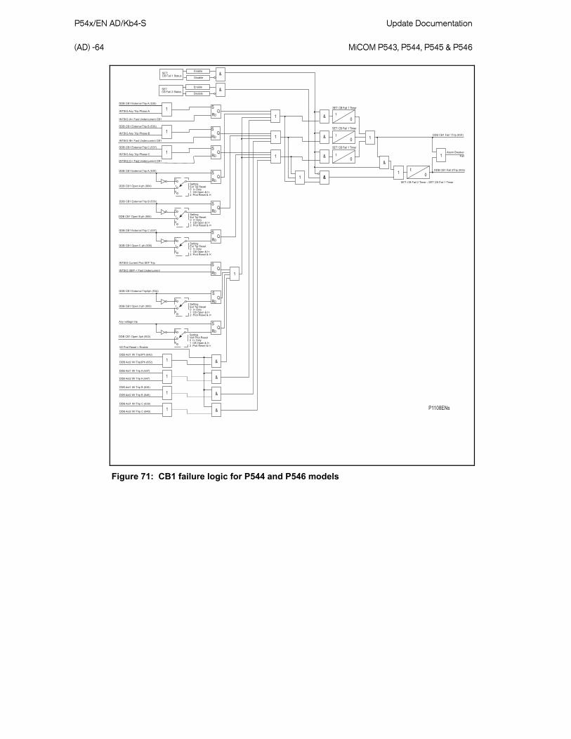
P54x/EN AD/Kb4-S Update Documentation
(AD) -64
MiCOM P543, P544, P545 & P546
���0�4 ����$�� ��"� 0�! ����
���0�4 �0�! 5 !�� 6�,$�#���$��
� ��� !�% ����� �&���-
-
-
-
0��� �� !�% � ��/$�
�
�
�
�%�/ ��$8$�!�%
� ��� !�% ����� �&���
0����� !�% � 0����
��9%$
��9%$
-�
�
��
-
�-
�
�
�
-�
0
12
02
02
02
�
�
�
� ��� �:�$��% ���� � �����
���0�4 ��) ���� ���$ �
���0�4 ��5 !�� 6�,$�#���$�� ���
� ��� �:�$��% ���� � �����
���0�4 ��5 !�� 6�,$�#���$�� ���
� ��� �:�$��% ���� � ���(�
���0�4 ��5 !�� 6�,$�#���$�� ���
���0�4 ��) ���� ���$ �
���0�4 ��) ���� ���$ �
� ��� �:�$��% ���� � �����
� ��� ��$� � �� � ���0$����3�:� ��� 1$�$�� �5 ��%)� �� ��$� - �5� ��"� 1$�$� - �5
02
� ��� �:�$��% ���� � �����
� ��� ��$� � �� � ���0$����3�:� ��� 1$�$�� �5 ��%)� �� ��$� - �5� ��"� 1$�$� - �5
02
02
�
� ��� �:�$��% ���� � ���(�
� ��� ��$� � �� � ���0$����3�:� ��� 1$�$�� �5 ��%)� �� ��$� - �5� ��"� 1$�$� - �5
02
0��� �� !�% � ��/$�
� ��� �:�$��% ������� �����
� ��� ��$� � �� � ���
0��� �� !�% � ��/$�
0$����3�:� ��� 1$�$�� �5 ��%)� �� ��$� - �5� ��"� 1$�$� - �5
0��� �� !�% � ��/$� ; 0�� �� !�% � ��/$�
�
�
�
����&���
1
1
1
1
1
1
1
0����� !�% � 0����
��9%$
��9%$
02
0$����3<"%� ��"� 1$�$�� �5 ��%)� �� ��$� - �5� ��"� 1$�$� - �5
1
��) ="%�3$ ����
�
� ��� ��$� ��� � ���
� ��,� >� ������� �����
�� ��,� >� ���� � ���(�
� ��,� >� ���� � ���(�
-� ��,� >� ������� �����
-
�� ��,� >� ���� � ���&�
� ��,� >� ���� � ���&� -
�� ��,� >� ���� � ��� �
� ��,� >� ���� � ��� � -
�
�
�
�
�
�
�
�
�
�
�
�
�
�
�
>� ��"� 1$�$� + ��9%$
Figure 71: CB1 failure logic for P544 and P546 models

Update Documentation P54x/EN AD/Kb4 MiCOM P543, P544, P545 & P546
(AD) -65
���0�4 ����$�� ��"� 0�! ����
���0�4 �0�! 5 !�� 6�,$�#���$��
� ��� !�% ����� �&���-
-
-
-
0��� �� !�% � ��/$�
�
�
�
�%�/ ��$8$�!�%
� ��� !�% ����� �&�(�
0����� !�% � 0����
��9%$
��9%$
-�
�
��
-
�-
�
�
�
-�
0
12
02
02
02
�
�
�
� ��� �:�$��% ���� � ��� �
���0�4 ��) ���� ���$ �
���0�4 ��5 !�� 6�,$�#���$�� ���
� ��� �:�$��% ���� � �����
���0�4 ��5 !�� 6�,$�#���$�� ���
� ��� �:�$��% ���� � �����
���0�4 ��5 !�� 6�,$�#���$�� ���
���0�4 ��) ���� ���$ �
���0�4 ��) ���� ���$ �
� ��� �:�$��% ���� � ��� �
� ��� ��$� � �� � ���0$����3�:� ��� 1$�$�� �5 ��%)� �� ��$� - �5� ��"� 1$�$� - �5
02
� ��� �:�$��% ���� � �����
� ��� ��$� � �� � ���0$����3�:� ��� 1$�$�� �5 ��%)� �� ��$� - �5� ��"� 1$�$� - �5
02
02
�
� ��� �:�$��% ���� � �����
� ��� ��$� � �� � ���0$����3�:� ��� 1$�$�� �5 ��%)� �� ��$� - �5� ��"� 1$�$� - �5
02
0��� �� !�% � ��/$�
� ��� �:�$��% ������� ���&�
� ��� ��$� � �� � ���
0��� �� !�% � ��/$�
0$����3�:� ��� 1$�$�� �5 ��%)� �� ��$� - �5� ��"� 1$�$� - �5
0��� �� !�% � ��/$� ; 0�� �� !�% � ��/$�
�
�
�
����&���
1
1
1
1
1
1
1
0����� !�% � 0����
��9%$
��9%$
02
0$����3<"%� ��"� 1$�$�� �5 ��%)� �� ��$� - �5� ��"� 1$�$� - �5
1
��) ="%�3$ ����
�
� ��� ��$� ��� � ���
� ��,� >� ������� �����
�� ��,� >� ���� � ���(�
� ��,� >� ���� � ���(�
-� ��,� >� ������� �����
-
�� ��,� >� ���� � ���&�
� ��,� >� ���� � ���&� -
�� ��,� >� ���� � ��� �
� ��,� >� ���� � ��� � -
�
�
�
�
�
�
�
�
�
�
�
�
�
�
�
>� ��"� 1$�$� + ��9%$
Figure 72: CB2 failure logic for P544 and P546 models
2.1.6 Switched Communication Networks
The P54x relays make use of digital communication signaling channels for the differential protection. For correct operation of this protection element, it is essential that the integrity of this link is continuously checked. For P54x relays, when GPS is not used it is also a requirement of this link that ‘go’ (tp1) and ‘return’ (tp2) times are similar (a difference of up to 1 ms can be tolerated). Times greater than this can result in relay instability.
Where switched communications networks are used, it is possible that during switching, a transient time period may exist with different ‘go’ and ‘return’ times. All P54x relays include a facility to ensure protection stability during this transient period.
One of the checks performed on the communications link is a check on the calculated propagation delay for each data message. During normal operation the difference in calculated time should be minimal (possible delays being introduced by multiplexers or other intermediary communication equipment). If successive calculated propagation delay times exceed a user settable value (250 – 1000 s). The P54x raise a comm delay alarm and initiate a change in relay setting for a short time period (Char Mod Time setting) to overcome any switching delay. This change in setting is shown in Figure 79 whereby the relay bias setting, k1, is increased to 200%. This characteristic provides stability for all load conditions and will still allow tripping for most internal fault conditions.

P54x/EN AD/Kb4-S Update Documentation
(AD) -66
MiCOM P543, P544, P545 & P546
Figure 73 shows a possible scenario for a switched network. Initially the P54x relays are communicating via path 1. The go and return times for this path are 2 ms and hence the calculated propagation delay is (2 + 2)/2 = 2 ms. When the channel is switched to path 2, a small time period exists where the P54x’s could be sending messages via path 1 and returning via path 2.
The calculated propagation delay will now be (2 + 5)/2 = 3.5 ms. The resultant 1.5 ms error at each line end may cause the relay to maloperate due to incorrect time alignment of current vectors (see section 1.1.1.1). After a short delay, both ‘go’ and ‘return’ paths will follow route 2 and the calculated propagation delay will be (5 + 5)/2 = 5 ms. The relay will now be stable, as correct current vector time alignment exists at each line end.
The Char Mod timer is started when a change in propagation delay is detected. Any subsequent change during this period will cause the timer to restart. In the above example the timer will start for the first change (2 to 3.5 ms). The second change (3.5 ms to 5 ms) will cause the timer to restart, therefore allowing for multiple switching between communication paths.
A change in propagation delay may result in a temporary failure of the protection communications channel. If this occurs, the propagation delay change may not be detected by the relay. To overcome this problem, the Char Mod Timer is re-started when the channel recovers from a protection communications channel failure if the Char Mod Timer was running when the channel failure occurred.
When Char Mod Ex is enabled and if the Char Mod Time has started then the Char Mod Ex Timer runs. If at the end of this timer and until Char Mod Time has expired, the bias current is above 5% In, and differential current is below 10% of bias current on all phases, then the Char Mod Time will reset and the characteristic will return to normal. If these conditions are not met, then the characteristic remains increased for the duration of the Char Mod Time. Char Mod Ex Timer should be set greater than the minimum switching delay expected, and less than Char Mod Time.

Update Documentation P54x/EN AD/Kb4 MiCOM P543, P544, P545 & P546
(AD) -67
��((*� �. ���&� ��.��*��
<����/.��(*����*&��.*�����=:���.�6��/*&;
/*&
�� "4 ���.���,��*�� �����
�&(
�>�&(
�&(
��&&4�*"'��*��
?4*�&��
��&&4�*"'��*��
?4*�&��������
@,�@�5��&(
@.�4.�@�5��&(
������
@,�@�5��&(
@.�4.�@�5��&(
��������
Figure 78: Switched communication network

P54x/EN AD/Kb4-S Update Documentation
(AD) -68
MiCOM P543, P544, P545 & P546
Figure 79: Transient bias characteristic
2.1.13 Unconditioned 2 Wire Pilot Communications for Distances Greater than 1.2 km
When communicating via a pair of unconditioned pilots for distances greater than 1.2 km, a leased line or baseband modem can be used. For maximum security and performance it is strongly recommended that a screened twisted pair of 0.5 mm (or greater) conductors are used. When choosing between leased line or baseband modems the following aspects should be considered:
� Leased line modems have a maximum transmission speed of 19.2 kbit/sec., whereas baseband modems can transmit at 64 kbit/sec.
� Baseband modems have longer re-training times, typically between 10 to 60 s. If the connection between is temporarily lost, the protection communications will be interrupted until the re-training period has elapsed.
� Since baseband modems use synchronous communication protocols, there is typically a 20% performance gain over leased line modems that use asynchronous protocols.
Modems tested:
� Keymile LineRunner DTM modem with G703 interface.
Type Max distance (km) Recommended data rate (kbit/sec)
Typical re-train time (seconds)
“Campus” 1092A (Obsolete) 17.2 64 10
LineRunner DTM 19.8 64 44

Update Documentation P54x/EN AD/Kb4 MiCOM P543, P544, P545 & P546
(AD) -69
2.2 InterMiCOM
2.2.1 Protection Signaling
In order to achieve fast fault clearance and correct discrimination for faults anywhere within a high voltage power network, it is necessary to signal between the points at which protection relays are connected. Two distinct types of protection signaling can be identified:
Unit protection schemes:
In these schemes the signaling channel is used to convey analog data representative of the power system between relays. Typically current magnitude and/or phase information is communicated between line ends to enable a unit protection scheme to be implemented. These unit protection schemes are not covered by InterMiCOM or InterMiCOM64. Instead, the MiCOM P52x and P54x range of current differential and phase comparison relays are available for unit applications.
Teleprotection - channel aided schemes:
In channel-aided schemes the signaling channel is used to convey simple ON/OFF commands from a local protection device to a remote device to provide some additional information to be used in the protection scheme operation. The commands can be used to accelerate in-zone fault clearance and/or prevent out-of-zone tripping.
The InterMiCOM application is an effective replacement to the traditional hardwired logic and communication schemes used by protection relays for such teleprotection signaling.
The MiCOM Px4x series products have a grouping of internal digital signals known as the digital data bus, DDB, that are used to implement the protection scheme logic. A number of these DDB signals are reserved as inputs and outputs for the InterMiCOM application. These are mapped using the programmable scheme logic (PSL) support tool. The InterMiCOM application provides a means of transferring the status of these mapped DDB signals between the protection relays using dedicated full-duplex communications channels.
2.2.2 InterMiCOM Variants
There are 2 different types of integrated InterMiCOM teleprotection available in the MiCOM P54x relays:
� An optical fiber implementation, InterMiCOM64 - designed, primarily, to work over fiber optic and multiplexed digital communications channels with data rates of 56/64 kbit/s. A total of sixteen InterMiCOM64 commands (16 inputs and 16 outputs) are available in the P54x. These are arranged as two groups of 8 bits each, and are referred to as Channel 1 and Channel 2. Three InterMiCOM64 scheme arrangements are possible:
� Two-terminal with a single communications link � Two-terminal with a dual redundant communications link (sometimes referred to as hot
standby) � Three terminal (or triangulated) scheme � An electrical implementation of InterMiCOM, realised over an EIA(RS)232 medium
typically for MODEM applications and referred to as MODEM InterMiCOM for ease of differentiation with InterMiCOM64. MODEM InterMiCOM supports two-terminal applications with a single communications channel. Eight MODEM InterMiCOM commands can be transmitted between the line ends.
Provided the correct hardware options have been specified, it is possible to configure the P54x to operate using either InterMiCOM64 or MODEM InterMiCOM or both. The selection is made under the CONFIGURATION column of the menu software.
2.2.3 InterMiCOM Features
The different requirements of applications that use teleprotection signaling for direct acting, permissive, or blocking schemes are all catered for by InterMiCOM.
Communications are supervised and alarms and signal defaults can be defined to give controlled actions in the event of communications signals being distorted or unavailable.

P54x/EN AD/Kb4-S Update Documentation
(AD) -70
MiCOM P543, P544, P545 & P546
Communications statistics and loopback features are available to help with commissioning and testing purposes.
Both, InterMiCOM64 and MODEM InterMiCOM teleprotection provide the ideal means to configure the schemes in the MiCOMho P443/P446 relay. The selection between the two will generally depend on communications media availability, system configuration, distances, cost issues and utility practice.
2.2.4 Definition of Teleprotection Commands
Three generic types of teleprotection command can be defined. These are Intertripping, Permissive signaling, and Blocking. All teleprotection signals are initiated in a transmitting relay but, according to the application, the receiving relay may condition the signal according to the scheme requirements:
Intertripping In intertripping (also called direct or transfer tripping) applications, the command is not supervised at the receiving end by any protection relay and its receipt causes direct circuit breaker operation. Since no checking of the received signal by another protection element is performed, it is essential that any noise on the signaling channel is not interpreted as being a valid signal when the command isn’t being transmitted. For an intertripping scheme, therefore, the primary requirement of the signaling channel is security.
Permissive In permissive applications, tripping is only permitted when the command coincides with a protection operation at the receiving end. Since the receiver applies a second independent check before tripping, the signaling channel for a permissive scheme does not have to be quite as secure as for an intertripping scheme, but it may need to be faster.
Blocking In blocking applications, tripping occurs when a protection element picks up in a receiving relay whilst no signal is received from a remote relay. In such schemes, when the command is received, the protection element is blocked even if a protection element picks up. Since the signal is used to prevent tripping, it is a requirement that the signal should be available whenever possible, and that it should be received as quickly as possible. The requirements of a blocking channel are, therefore, to be fast and to be dependable.
The requirements for the three channel types are represented pictorially in Figure 81.
�������� �� ��!������
� ��!
"#
$�����
�"#��
%��%
������&�������
��� ����'�
("�)���
���*+���
Figure 81: Pictorial comparison of operating modes

Update Documentation P54x/EN AD/Kb4 MiCOM P543, P544, P545 & P546
(AD) -71
This diagram shows that a blocking signal should be fast and dependable; a direct intertrip signal should be very secure; and a permissive signal is an intermediate compromise of speed, security and dependability.
In MODEM InterMiCOM applications, selected signaling bits within each message can be conditioned to provide optimal characteristics for each type of the three teleprotection command types.
In InterMiCOM64 applications, the framing and error checking of a single command message is sufficient to meet the security of a permissive application, whilst the speed is sufficiently fast to meet the needs of a blocking scheme. Accordingly in InterMiCOM64 applications, there is no differentiation between blocking commands or permissive commands, so that only signals being used for direct intertripping with higher security requirements need to be differentiated from those in permissive (or blocking) schemes.
2.3 MODEM InterMiCOM, EIA(RS)232 InterMiCOM or Copper InterMiCOM
2.3.1 Communications Media
MODEM InterMiCOM is capable of transferring up to eight commands over one communication channel. Due to recent expansions in communication networks, most signaling channels are now digital schemes utilizing multiplexed communications links and for this reason, MODEM InterMiCOM provides a standard EIA(RS)232 output using digital signaling techniques. This digital signal can then be converted using suitable devices to a range of different communications media as required. The EIA(RS)232 output may alternatively be connected to MODEMs for use over analogue links.
Regardless of whether analogue or digital systems are being used, all the requirements of teleprotection commands are described by an international standard, IEC60834-1:1999, and MODEM InterMiCOM is compliant with the essential requirements of this standard. This standard describes the speed requirements of the commands as well as the security (defined in terms of probability of unwanted commands being received) and dependability (defined in terms of the probability of missing commands).
2.3.2 General Features and Implementation
InterMiCOM provides eight commands over a single communications link, with the mode of operation of each command being individually selectable within the IM# Cmd Type cell. Blocking mode provides the fastest signaling speed (available on commands 1 - 4), Direct Intertrip mode provides the most secure signaling (available on commands 1 - 8) and Permissive mode provides secure, dependable signaling (available on commands 5 - 8). Each command can also be disabled so that it has no effect in the logic of the relay.
Since many applications involve commands being sent over a multiplexed communications channel, it is necessary to ensure that only data from the correct relay is used. The relays in the scheme must be programmed with a unique pair of addresses that correspond with each other in the Source Address and Receive Address cells. For example, at the local end relay, if the Source Address is set to 1, the Receive Address at the remote end relay must also be set to 1. Similarly, if the remote end relay has a Source Address set to 2, the Receive Address at the local end must also be set to 2. The two pairs of addresses should be set to be different in any scheme to avoid the possibility of incorrect operation during inadvertent loopback connections, and any schemes sharing the same communications services should be set to have different address pairs in order to avoid any problems caused by inadvertent cross-channel connections.
Noise on the communications should not be interpreted as valid commands by the relay. For this reason, InterMiCOM uses a combination of unique pair addressing described above, basic signal format checking and an 8-bit Cyclic Redundancy Check (CRC) according to the security requirements of the commands. The CRC calculation is performed at both the sending and receiving end relays for each message and both must match in order to assure the security of the Direct Intertrip commands.
An alarm is provided if noise on the communications channel becomes excessive.

P54x/EN AD/Kb4-S Update Documentation
(AD) -72
MiCOM P543, P544, P545 & P546
During periods of excessive noise, it is possible that the synchronization of the message structure will be lost and accurate decoding of the messages may not be possible. Predictable operation of InterMiCOM is assured during such noisy periods by means of the IM# FallBackMode cell. The status of the last received valid command can be maintained until a new valid message is received by setting the IM# FallBackMode cell to Latched. Alternatively, a known fallback state can be assigned to the command by setting the IM# FallBackMode cell to Default. In this latter case, the time period between communication disruption and the default state being restored will need to be set in the IM# FrameSynTim cell and the default value will need to be set in IM# DefaultValue cell. Upon subsequent receipt of a valid message, all the timer periods will be reset and the new valid command states will be used.
If there is a total communications failure, the relay will use the fallback (failsafe) strategy as described above. Total failure of the channel is considered when no message data is received for four power system cycles or if there is a loss of the DCD line.
2.3.3 EIA(RS)232 Physical Connections
MODEM InterMiCOM on the Px4x relays is implemented using a 9-pin D type female connector (labeled SK5) located at the bottom of the Second Rear communication board. This connector on the Px40 relay is wired in DTE (Data Terminating Equipment) mode, as indicated below:
Pin Acronym InterMiCOM Usage
1 DCD Data Carrier Detect is only used when connecting to modems otherwise this should be tied high by connecting to terminal 4
2 RxD Receive Data
3 TxD Transmit Data
4 DTR Data Terminal Ready is permanently tied high by the hardware since InterMiCOM requires a permanently open communication channel
5 GND Signal Ground
6 Not used -
7 RTS Ready To Send is permanently tied high by the hardware since InterMiCOM requires a permanently open communication channel
8 Not used -
9 Not used -
Dependant upon whether a direct or modem connection between the two relays in the scheme is being used, the required pin connections are described as follows:
2.3.4 Direct Connection
EIA(RS)232 is only suitable for short transmission distances due to the signaling levels used and the connection shown below is limited to less than 15 m. This limit may be overcome by introducing suitable signal converters as described in the following sections:

Update Documentation P54x/EN AD/Kb4 MiCOM P543, P544, P545 & P546
(AD) -73
��*��,����#��%&������-.�
�+�*���/0
�+�*���/0
��*��,����#��%&������-.�
�-�,��1���1,2��
,1�
�-�,��1���1,2��
,1�
33333
3
33333
3
��������
Figure 82: Direct connection within the local substation
The connection configuration shown in Figure 82 should also be used when connecting to equipment that does not implement control the DCD line.
2.3.5 EIA(RS)232 Modem Connection
To achieve longer distance communication, modems may be used, in which the case the following connections should be made.
��*��,����#��%&������-.�
�+�*���/0
�+�*���/0
��*��,����#��%&������-.�
�-�,��1���1,2��
,1�
�-�,��1���1,2��
,1�
33333
3
33333
3
���*����
�-�,��1��
2��
�-�,��1��
2��
-" �������"����#"�)
Figure 83: InterMiCOM teleprotection via a MODEM link
This type of connection should be used when connecting to multiplexers which provide an EIA(RS)232 channel with the ability to control the DCD line. With this type of connection it should be noted that the maximum distance between the Px40 relay and the modem should not exceed 15 m, and that a baud rate suitable for the communications path used should be selected.
2.3.6 RS422 Connection
An RS232 to RS422 converter such as Schneider Electric CK212 may be employed to enable MODEM InterMiCOM to be applied if 4-wire pilots are available for signaling as shown in the example below.

P54x/EN AD/Kb4-S Update Documentation
(AD) -74
MiCOM P543, P544, P545 & P546
Px4x Relay with InterMiCOM
RS232(SK5)
(6)-(9)Rx (2)Tx (3)
GND (5)5v (4)
DCD (1)
RS232/RS422
(6)-(9)(2) Rx(3) Tx (5) GND
X5
ConnectorsD1+(5)D1- (4)D2- (6)D2+(3)
+5v GND (1) (2)
+5 v GND
DC Power Supply
Px4x Relay with InterMiCOM
RS232(SK5)
(6)-(9)(2) Rx (3) Tx
(4) 5v (1) DCD
(5) GND
RS232/RS422
X5
Connectors
(3)D2+(6)D2-(4)D1-(5)D1+
+5v GND (1) (2)
(6)-(9)Rx (2) Tx (3)
GND (5)
GND GND
P4332ENa
RS422 InterMiCOM (similar to RS485)
+5 v GND
DC Power Supply
Figure 84: MODEM InterMiCOM teleprotection via a RS422 protocol
Using an appropriate converter, pilots of up to 1.2km in length can be used, depending on the converter performance.
In this case, the maximum distance between the Px40 relay and the converter should not exceed 15 m.
2.3.7 Fiber Optic Connection
Although InterMiCOM64 is the recommended variant of InterMiCOM for use with optical fiber connections, MODEM InterMiCOM may also be applied over optical fibers by means of EIA(RS)232 to fiber optic converters. In this the case the following connections should be made:
Figure 85: MODEM InterMiCOM teleprotection via fiber optic
The overall fiber length that can be achieved depends on the converter performance.
In this case, the maximum distance between the Px40 relay and the converter should not exceed 15 m.
CK212CK212

Update Documentation P54x/EN AD/Kb4 MiCOM P543, P544, P545 & P546
(AD) -75
2.3.8 InterMiCOM Functional Assignment
The settings to control the mode of the intertrip signals are made using the relay’s menu software. In addition to this, it is necessary to assign InterMiCOM input and output signals in the relay Programmable Scheme Logic (PSL) editor. Two icons are provided on the PSL editor of MiCOM S1 (S1 Studio) for Integral tripping In and Integral tripping out which can be used to assign the eight intertripping commands. The example shown in figure 48 shows a Control Input_1 connected to the Intertrip O/P1 signal which would then be transmitted to the remote end. At the remote end, the Intertrip I/P1 signal would then be assigned within the PSL. In this example, we can see that when intertrip signal 1 is received from the remote relay, the local end relay would operate an output contact, R1.
Figure 86: Example assignment of signals within the PSL
Note: When an InterMiCOM signal is sent from the local relay, only the remote end relay will react to this command. The local end relay will only react to InterMiCOM commands initiated at the remote end and received locally, and vice-versa. InterMiCOM can, therefore, be described as a duplex teleprotection system.
2.3.9 InterMiCOM Statistics and Diagnostics
MODEM InterMiCOM channel statistics and diagnostics are available via the menu software. These can be hidden, according to preference, by setting the Ch Statistics and/or Ch Diagnostics cells to Invisible. All channel statistics are reset when the relay is powered up, or by user selection by means of the Reset Statistics cell.
3.8 Read Only Mode
With IEC 61850 and Ethernet/Internet communication capabilities, security has become a pressing issue. The Px40 relay provides a facility to allow the user to enable or disable the change in configuration remotely. This feature is available only in relays with Courier, Courier with IEC 60870-5-103 and Courier with IEC 61850 protocol options. It has to be noted that in IEC 60870-5-103 protocol, Read Only Mode function is different from the existing Command block feature.

P54x/EN AD/Kb4-S Update Documentation
(AD) -76
MiCOM P543, P544, P545 & P546 3.8.1 Protocol/port Implementation:
3.8.1.1 IEC 60870-5-103 Protocol on Rear Port 1:
The protocol does not support settings but the indications, measurands and disturbance records commands are available at the interface.
Allowed:
Poll Class 1 (read spontaneous events)
Poll Class 2 (read measurands)
GI sequence (ASDU7 'Start GI', Poll Class 1)
Transmission of Disturbance Records sequence (ASDU24, ASDU25, Poll Class 1)
Time Synchronization (ASDU6)
General Commands (ASDU20), namely:
INF23 activate characteristic 1
INF24 activate characteristic 2
INF25 activate characteristic 3
INF26 activate characteristic 4
Blocked:
Write parameter (=change setting) (private ASDUs)
General Commands (ASDU20), namely:
INF16 auto-recloser on/off
INF19 LED reset
Private INFs (e.g. CB open/close, control inputs)
3.8.1.2 Courier Protocol on Rear Port 1/2 and Ethernet
Allowed:
Read settings, statuses, measurands
Read records (event, fault, disturbance)
Time Synchronization
Change active setting group
Blocked:
Write settings
All controls, including:
Reset Indication (Trip LED)
Operate control inputs
CB operations
Auto-reclose operations
Reset demands
Clear event/fault/maintenance/disturbance records
Test LEDs & contacts

Update Documentation P54x/EN AD/Kb4 MiCOM P543, P544, P545 & P546
(AD) -77
3.8.1.3 IEC 61850
Allowed:
Read statuses, measurands
Generate reports
Extract disturbance records
Time synchronization
Change active setting group
Blocked:
All controls, including:
Enable/disable protection
Operate control inputs
CB operations (Close/Trip, Lock)
Reset LEDs
3.8.2 Courier Database Support
Three new settings, one for each remote communications port at the back of the relay are created to support the enabling and disabling of the Read Only mode at each port.
The NIC Read Only setting will apply to all the communications protocols (including the Tunnelled Courier) that are transmitted via the Ethernet Port. Their default values are Disabled.
The DNP3 communication interface that do not support the feature will ignore these settings.
3.8.3 New DDB Signals
The remote Read Only mode is also available in the PSL via three dedicated DDB signals:
� RP1 Read Only � RP2 Read Only � NIC Read Only Through careful scheme logic design, the activations of these Read Only signals can be facilitated via Opto Inputs, Control Inputs and Function Keys.
These DDBs are available in every build, however they are effective only in Courier, IEC 60870-5-103 build and in latest IEC 61850 (firmware version 57 onwards). The setting cells are not available in DNP3.0.
APPLICATION NOTES (P54x/EN AP/Ja4)
2.1.4 Transformers in zone applications (P543 and P545 models) In applying the well established principles of differential protection to transformers, a variety of considerations have to be taken into account. These include compensation for any phase shift across the transformer, possible unbalance of signals from current transformers either side of windings, and the effects of the variety of earthing and winding arrangements. In addition to these factors, which can be compensated for by correct application of the relay, the effects of normal system conditions on relay operation must also be considered. The differential element must restrain for system conditions which could result in maloperation of the relay, such as high levels of magnetizing current during inrush conditions.

P54x/EN AD/Kb4-S Update Documentation
(AD) -78
MiCOM P543, P544, P545 & P546
In traditional transformer feeder differential schemes, the requirements for phase and ratio correction were met by correct selection of line current transformers. In the P543 and P545, software interposing CTs (ICTs) are provided which can give the required compensation. The advantage of having replica interposing CTs is that it gives the P54x relays the flexibility to cater for line CTs connected in either star or delta, as well as being able to compensate for a variety of system earthing arrangements. The P543 and P545 relays also include a magnetizing inrush restraint and blocking facility.
Note: The P544 and P546 relays do not include any of the above features, except CT ratio mismatch compensation, and as such would not be suitable for the protection of in-zone transformer feeders.
2.1.4.1 Magnetizing Inrush Stabilization (P543 and P545)
When a transformer is first energized, a transient magnetizing current flows, which may reach instantaneous peaks of 8 to 30 times the full load current. The factors controlling the duration and magnitude of the magnetizing inrush are:
� Size of the transformer bank � Size of the power system � Resistance in the power system from the source to the transformer bank � Residual flux level � Type of iron used for the core and its saturation level. � There are three conditions which can produce a magnetizing inrush effect: � First energization � Voltage recovery following external fault clearance � Sympathetic inrush due to a parallel transformer being energized. Figure 1 shows under normal steady state conditions the flux in the core changes from maximum negative value to maximum positive value during one half of the voltage cycle, which is a change of 2.0 maximum.
Figure 1: Steady state magnetizing inrush current
If the transformer is energized at a voltage zero when the flux would normally be at its maximum negative value, the flux will rise to twice its normal value over the first half cycle of voltage. To establish this flux, a high magnetizing inrush current is required. The first peak of this current can be as high as 30 times the transformer rated current. This initial rise could be further increased if there was any residual flux in the core at the moment the transformer was energized.

Update Documentation P54x/EN AD/Kb4 MiCOM P543, P544, P545 & P546
(AD) -79
Figure 2: Magnetizing inrush current during energization
As the flux enters the highly saturated portion of the magnetizing characteristic, the inductance falls and the current rises rapidly. Magnetizing impedance is of the order of 2000% but under heavily saturated conditions this can reduce to around 40%, which is an increase in magnetizing current of 50 times normal. This figure can represent 5 or 6 times normal full load current.
Analysis of a typical magnitude inrush current wave shows (fundamental = 100%):
Component -DC 2nd H 3rd H 4th H 5th H 6th H 7th H
55% 63% 26.8% 5.1% 4.1% 3.7% 2.4%
The offset in the wave is only restored to normal by the circuit losses. The time constant of the transient can be quite long, typically 0.1 second for a 100 KVA transformer and up to 1 second for larger units. The initial rate of decay is high due to the low value of air core reactance. When below saturation level, the rate of decay is much slower. The following graph shows the rate of decay of the DC offset in a 50 Hz or 60 Hz system in terms of amplitude reduction factor between successive peaks.

P54x/EN AD/Kb4-S Update Documentation
(AD) -80
MiCOM P543, P544, P545 & P546
Variation of amplitude reduction factor between successive mMagnetising inrush peaks with X/R ratio
0.2
0.3
0.4
0.5
0.6
0.7
0.8
0.9
1
0 10 20 30 40 50 60 70 80 90 100
X/R ratio
Am
plitu
de re
duct
ion
fact
or (k
)
P4299ENa
Figure 3: Variation of amplitude reduction factor
The magnitude of the inrush current is limited by the air core inductance of the windings under extreme saturation conditions. A transformer with concentric windings will draw a higher magnetizing current when energized from the LV side, since this winding is usually on the inside and has a lower air core inductance. Sandwich windings have approximately equal magnitude currents for both LV and HV. Resistance in the source will reduce the magnitude current and increase the rate of decay.
The magnetizing inrush phenomenon is associated with a transformer winding which is being energized where no balancing current is present in the other winding(s). This current appears as a large operating signal for the differential protection. Therefore, special measures are taken with the relay design to ensure that no maloperation occurs during inrush. The fact that the inrush current has a high proportion of harmonics having twice the system frequency offers a possibility of stabilization against tripping by the inrush current.
The P543 and P545 relay provides a choice between harmonic restraint and blocking by setting option, both providing stability during transformer inrush conditions.
To select second harmonic Restraint or Blocking option, set the cell [3312: Inrush Restraint] under the GROUP 1 PHASE DIFF menu heading to Restraint or Blocking. Second harmonic restraints or blocking provide security during transformer energization.

Update Documentation P54x/EN AD/Kb4 MiCOM P543, P544, P545 & P546
(AD) -81
2.1.4.2 Second Harmonic Restraint (P543 and P545)
The magnetizing inrush current contains a high percentage of second harmonic. The P543 and P545 relays filter out this component of the waveform and use it as an additional bias quantity. The total bias used by the relay will therefore be a combination of the average load current on the line plus a multiple of the second harmonic component of the current. The multiplying factor which is used to ensure stability is controlled by the setting cell [3314: Ih(2) Multiplier] under the GROUP 1 PHASE DIFF menu heading provided the setting cell [ 3312: Inrush Restraint ] is set to Restraint .
This multiplier is used in additional bias calculation as per following formula:
IF Inrush Restraint setting is set to Restraint
Additional bias = Ih(2) Multiplier * 1.414 * largest 2nd harmonic current
ELSE
Additional bias = 0
In the above equation second harmonic current is derived from Fourier filtering techniques.
Where P543 and P545 relays are used and inrush restrain function is enabled, it must be ensured that this function is enabled at each end to avoid possible maloperation.
2.1.4.3 Second Harmonic Blocking (P543 and P545)
To select second harmonic blocking option, set the cell [3312: Inrush Restraint] under the GROUP 1 PHASE DIFF menu heading to Blocking.
Second harmonic blocking provides security during transformer energization.
For each phase, if the level of phase current is above 5% In, and if the ratio of second harmonic current ,Ih(2) to fundamental in the line is above the settings at cell [3320: Ih(2) >%] then inrush conditions shall be detected which sets the appropriate phase block, to block local and remote ends.
Users can choose to apply Cross blocking or independent blocking by choosing the appropriate setting at cell [3321: Ih(2) CrossBlock] under the GROUP 1 PHASE DIFF menu heading. If Ih(2) CrossBlock is set to Disabled then independent blocking is used.
If independent blocking is enabled only the affected phase is blocked at all ends. If cross blocking is enabled all phases are blocked at all ends.
2.1.4.4 Fifth Harmonic Blocking (P543 and P545)
The fifth Harmonic blocking feature is available for possible use to prevent unwanted operation of the low set differential element under transient overfluxing conditions.
When overfluxing occurs, the transformer core becomes partially saturated and the resultant magnetizing current waveforms increase in magnitude and become harmonically distorted. Such waveforms have a significant fifth harmonic content, which can be extracted and used as a means of identifying the abnormal operating condition.
The fifth harmonic blocking threshold is adjustable between 5 - 100%. The threshold should be adjusted so that blocking will be effective when the magnetizing current rises above the chosen threshold setting of the low-set differential protection.
For example, when a load is suddenly disconnected from a power transformer the voltage at the input terminals of the transformer may rise by 10-20% of the rated value. Since the voltage increases, the flux, which is the integral of the excitation voltage, also increases. As a result, the transformer steady state excitation current becomes higher. The resulting excitation current flows in one winding only and therefore appears as differential current which may rise to a value high enough to operate the differential protection. A typical differential current waveform during such a condition is shown in Figure 4. A typical setting for Ih(5)%> is 35%

P54x/EN AD/Kb4-S Update Documentation
(AD) -82
MiCOM P543, P544, P545 & P546
P4353ENa
Figure 4: Typical overflux current waveform
To offer some protection against damage due to persistent overfluxing that might be caused by a geomagnetic disturbance, the fifth harmonic blocking element can be routed to an output contact using an associated timer. Operation of this element could be used to give an alarm to the network control centre. If such alarms are received from a number of transformers, they could serve as a warning of geomagnetic disturbance so that operators could take some action to safeguard the power system. Alternatively this element can be used to initiate tripping in the event of prolonged pick up of a fifth harmonic measuring element. It is not expected that this type of overfluxing condition would be detected by the AC overfluxing protection. This form of time delayed tripping should only be applied in regions where geomagnetic disturbances are a known problem and only after proper evaluation through simulation testing.
The P543 and P545 determine the fundamental components and the fifth harmonic components from the line currents and provide fifth harmonic blocking option when the setting cell [3312: Inrush Restraint] under the GROUP 1 PHASE DIFF menu is set to Blocking.
For each phase, if the level of phase current is above 5% In, and if the ratio of fifth harmonic current, Ih(5) to fundamental in the line is above the settings at cell [3328: Ih(5) >%] then the overfluxing conditions shall be detected which sets the appropriate phase block, to block local and remote ends.
Users can choose to apply Cross blocking or independent blocking by choosing the appropriate setting at cell [3329: Ih(5) CrossBlock] under the GROUP 1 PHASE DIFF menu heading. If Ih(5) CrossBlock is set to Disabled then independent blocking is used.
If independent blocking is enabled only the affected phase is blocked at all ends. If cross blocking is enabled all phases are blocked at all ends.
2.1.4.7 High Set Differential Setting (P543 and P545)
When Inrush Restraint is set to Restraint or Blocking, a high set differential protection becomes active. This is provided to ensure rapid clearance for heavy internal faults with saturated CTs. Because high set is not restrained by magnetizing inrush, hence the setting must be set such that it will not operate for the largest inrush currents expected. It is difficult to accurately predict the maximum anticipated level of inrush current. Typical waveforms peak values are of the order of 8-10x rated current. A worst case estimation of inrush could me made by dividing the transformer full load current by the per unit leakage reactance quoted by the transformer manufacturer.

Update Documentation P54x/EN AD/Kb4 MiCOM P543, P544, P545 & P546
(AD) -83
2.8.4 Restricted Earth Fault Protection
Earth faults occurring on a transformer winding or terminal may be of limited magnitude, either due to the impedance present in the earth path or by the percentage of transformer winding that is involved in the fault. It is common to apply standby earth fault protection fed from a single CT in the transformer earth connection - this provides time-delayed protection for a transformer winding or terminal fault. In general, particularly as the size of the transformer increases, it becomes unacceptable to rely on time delayed protection to clear winding or terminal faults as this would lead to an increased amount of damage to the transformer. A common requirement is therefore to provide instantaneous phase and earth fault protection. Applying differential protection across the transformer may fulfill these requirements. However, an earth fault occurring on the LV winding, particularly if it is of a limited level, may not be detected by the differential relay, as it is only measuring the corresponding HV current. Therefore, instantaneous protection that is restricted to operating for transformer earth faults only is applied. This is referred to as restricted earthfault protection (REF).
When applying differential protection such as REF, some suitable means must be employed to give the protection stability under external fault conditions, therefore ensuring that relay operation only occurs for faults on the transformer winding / connections.
Two methods are commonly used; bias or high impedance. The biasing technique operates by measuring the level of through current flowing and altering the relay sensitivity accordingly. The high impedance technique ensures that the relay circuit is of sufficiently high impedance such that the differential voltage that may occur under external fault conditions is less than that required to drive setting current through the relay.
The REF protection in the P54x relays can be configured to operate as high impedance element. Following sections describe the application of the relay for high impedance element.
Note: The high impedance REF element of the relay shares the same CT input as the SEF protection. Hence, only one of these elements may be selected.
2.8.4.1 Setting Guidelines for High Impedance Restricted Earth Fault (REF)
From the SEF/REF options cell, Hi Z REF must be selected to enable this protection. The only setting cell then visible is �REF>�s, which may be programmed with the required differential current setting. This would typically be set to give a primary operating current of either 30% of the minimum earth fault level for a resistance earthed system or between 10 and 60% of rated current for a solidly earthed system.
The primary operating current (�op) will be a function of the current transformer ratio, the relay operating current (�REF>�s1), the number of current transformers in parallel with a relay element (n) and the magnetizing current of each current transformer (�e) at the stability voltage (Vs). This relationship can be expressed in three ways:
1. To determine the maximum current transformer magnetizing current to achieve a specific primary operating current with a particular relay operating current:
�e < 1
n x ���
���
�op
CT ratio - �REF > �s
2. To determine the minimum relay current setting to achieve a specific primary operating current with a given current transformer magnetizing current.
[�REF > �s] < ���
���
�op
CT ratio - n�e

P54x/EN AD/Kb4-S Update Documentation
(AD) -84
MiCOM P543, P544, P545 & P546 2.8.4.2 Use of METROSIL Non-Linear Resistors
Metrosils are used to limit the peak voltage developed by the current transformers under internal fault conditions, to a value below the insulation level of the current transformers, relay and interconnecting leads, which are normally able to withstand 3000 V peak.
The following formulae should be used to estimate the peak transient voltage that can be produced for an internal fault. The peak voltage produced during an internal fault will be a function of the current transformer kneepoint voltage and the prospective voltage that would be produced for an internal fault if current transformer saturation did not occur.
Vp = 2 2Vk ( Vf - Vk )
Vf = �'f (Rct + 2RL + RST)
Where:Vp = Peak voltage developed by the CT under internal fault conditions
Vk = Current transformer kneepoint voltage
Vf = Maximum voltage that would be produced if CT saturation did not occur
�'f = Maximum internal secondary fault current
Rct = Current transformer secondary winding resistance
RL = Maximum lead burden from current transformer to relay
RST = Relay stabilizing resistor
When the value given by the formulae is greater than 3000 V peak, metrosils should be applied. They are connected across the relay circuit and serve the purpose of shunting the secondary current output of the current transformer from the relay in order to prevent very high secondary voltages.
Metrosils are externally mounted and take the form of annular discs. Their operating characteristics follow the expression:
V = C�0.25
Where:V = Instantaneous voltage applied to the non-linear resistor (metrosil)
C = Constant of the non-linear resistor (metrosil)
I = Instantaneous current through the non-linear resistor (metrosil)
With a sinusoidal voltage applied across the metrosil, the RMS current would be approximately 0.52 x the peak current. This current value can be calculated as follows:
Where: Vs(rms) = rms value of the sinusoidal voltage applied across the metrosil.
This is due to the fact that the current waveform through the metrosil is not sinusoidal but appreciably distorted.
For satisfactory application of a non-linear resistor (metrosil), it's characteristic should be such that it complies with the following requirements:
3. At the relay voltage setting, the non-linear resistor (metrosil) current should be as low as possible, but no greater than approximately 30 mA rms for 1 A current transformers and approximately 100 mA rms for 5 A current transformers.

Update Documentation P54x/EN AD/Kb4 MiCOM P543, P544, P545 & P546
(AD) -85
4. At the maximum secondary current, the non-linear resistor (metrosil) should limit the
voltage to 1500 V rms or 2120 V peak for 0.25 second. At higher relay voltage settings, it is not always possible to limit the fault voltage to 1500V rms, so higher fault voltages may have to be tolerated.
The following tables show the typical Metrosil types that will be required, depending on relay current rating, REF voltage setting etc.
5. Metrosil Units for Relays with a 1 Amp CT 6. The Metrosil units with 1 Amp CTs have been designed to comply with the following
restrictions: 7. At the relay voltage setting, the Metrosil current should be less than 30 mA rms. 8. At the maximum secondary internal fault current the Metrosil unit should limit the
voltage to 1500 V rms if possible. The Metrosil units normally recommended for use with 1Amp CT's are as shown in the following table:
Relay voltage setting
Nominal characteristic Recommended Metrosil type
C � Single pole relay Triple pole relay Up to 125 V rms 125 to 300 V rms 450 900 0.25 0.25 600 A/S1/S256 600
A/S1/S1088 600 A/S3/1/S802 600 A/S3/1/S1195
Note: Single pole Metrosil units are normally supplied without mounting brackets unless otherwise specified by the customer.
Metrosil units for relays with a 5 amp CT
These Metrosil units have been designed to comply with the following requirements:
9. At the relay voltage setting, the Metrosil current should be less than 100 mA rms (the actual maximum currents passed by the units shown below their type description.
10. At the maximum secondary internal fault current the Metrosil unit should limit the voltage to 1500 V rms for 0.25 secs. At the higher relay settings, it is not possible to limit the fault voltage to 1500 V rms hence higher fault voltages have to be tolerated (indicated by *, **, ***).
11. The Metrosil units normally recommended for use with 5 Amp CTs and single pole relays are as shown in the following table:
Secondary
internal fault
current Recommended Metrosil type
Relay voltage setting Amps rms Up to 200 V rms 250 V rms 275 V rms 300 V rms
50 A 600 A/S1/S1213
C = 540/640 35 mA rms
600 A/S1/S1214 C = 670/800 40 mA rms
600 A/S1/S1214 C =670/800 50 mA rms
600 A/S1/S1223 C = 740/870* 50 mA rms
100 A 600 A/S2/P/S1217 C
= 470/540 70 mA rms
600 A/S2/P/S1215 C = 570/670 75 mA rms
600 A/S2/P/S1215 C =570/670
100 mA rms
600 A/S2/P/S1196 C =620/740*
100 mA rms
150 A 600 A/S3/P/S1219 C
= 430/500 100 mA rms
600 A/S3/P/S1220 C = 520/620
100 mA rms
600 A/S3/P/S1221C = 570/670** 100 mA
rms
600 A/S3/P/S1222C =620/740*** 100 mA rm
Note: *2400 V peak **2200 V peak ***2600 V peak
In some situations single disc assemblies may be acceptable, contact Schneider Electric for detailed applications.
12. The Metrosil units recommended for use with 5 Amp CTs can also be applied for usewith triple pole relays and consist of three single pole units mounted on the same central stud but electrically insulated from each other. To order these units please specify Triple pole Metrosil type, followed by the single pole type reference.

P54x/EN AD/Kb4-S Update Documentation
(AD) -86
MiCOM P543, P544, P545 & P546
13. Metrosil units for higher relay voltage settings and fault currents can be supplied if required.
14. To express the protection primary operating current for a particular relay operating current and with a particular level of magnetizing current.
�op = (CT ratio) x (�REF > �s + n�c)
To achieve the required primary operating current with the current transformers that are used, a current setting (�REF>�s) must be selected for the high impedance element, as detailed in expression (ii) above. The setting of the stabilizing resistor (RST) must be calculated in the following manner, where the setting is a function of the required stability voltage setting (Vs) and the relay current setting (�REF>�s).
Rst = Vs
�REF>�s = �F (RCT + 2RL)
�REF > �s
Note: The above formula assumes negligible relay burden.
The stabilizing resistor that can be supplied is continuously adjustable up to its maximum declared resistance.
2.17 Integral Intertripping
The MiCOM P54x supports integral intertripping in the form of InterMiCOM. InterMiCOM can be realized using an auxiliary EIA(RS)232 connection (MODEM InterMiCOM), or it can be realised by means of an integral optical fiber communication connection (fiber InterMiCOM, or InterMiCOM64). EIA(RS)232 (MODEM) InterMiCOM provides a single, full duplex communication channel, suitable for connection between two MiCOM P54x. The fiber InterMiCOM (InterMiCOM64) can provide up to two full-duplex communications channels. It can be used to connect two MiCOM P54x using a single channel, or redundancy can be added by using dual communications. Alternatively, InterMiCOM64 can be used to connect three MiCOM P54x devices in a triangulated scheme for the protection of Teed feeders. MODEM InterMiCOM and InterMiCOM64 are completely independent. They have separate settings, are described by separate DDB signals.
As a general rule, where possible, InterMiCOM64 would be preferable from an application point of view since it is faster, and based on optical fibers it has high immunity to electro-magnetic interference. If the high speed communication channel requirement of InterMiCOM64 cannot be provided, EIA(RS)232 provides a cost effective alternative.
Because of the differences between the implementation of EIA(RS)232 InterMiCOM and InterMiCOM64, the settings associated with each implementation are different. Refer to P54x/EN ST for details of all settings. There are settings to prevent inadvertent cross-connection or loopback of communications channels (address settings), settings to accommodate different channel requirements (baud rate, clock source, channel selection) as well as the different settings used for channel quality monitoring and signal management actions in the event of channel failures.
The received InterMiCOM signals are continually monitored for quality and availability. In the event of quality or availability of the received signals falling below set levels, then an alarm can be raised.
Note: An alarm indicating the signaling has failed, refers only to the incoming signals. The remote relay will monitor the other direction of the communications link for quality of transmission. If indication of the quality of the signal transmitted from the local relay for reception at the remote relay is required, then one of the InterMiCOM command channels can be used to reflect this back.

Update Documentation P54x/EN AD/Kb4 MiCOM P543, P544, P545 & P546
(AD) -87
2.17.1 EIA(RS)232 InterMiCOM (“Modem InterMiCOM”)
The settings necessary for the implementation of MODEM InterMiCOM are contained within two columns of the relay menu structure. The first column entitled INTERMICOM COMMS contains all the information to configure the communication channel and also contains the channel statistics and diagnostic facilities. The second column entitled INTERMICOM CONF selects the format of each signal and its fallback operation mode.
The settings required for the InterMiCOM signaling are largely dependant upon whether a direct or indirect (modem/multiplexed) connection between the scheme ends is used.
Direct connections will either be short metallic or dedicated fiber optic based (by means of suitable EIA 232 to optical fiber converters) and hence can be set to have the highest signaling speed of 19200b/s. Due to this high signaling rate, the difference in operating speed between the direct, permissive and blocking type signals is so small that the most secure signaling (direct intertrip) can be selected without any significant loss of speed. In turn, since the direct intertrip signaling requires the full checking of the message frame structure and CRC checks, it would seem prudent that the IM# Fallback Mode be set to Default with a minimal intentional delay by setting IM# FrameSyncTim to 10 msecs. In other words, whenever two consecutive messages have an invalid structure, the relay will immediately revert to the default value until a new valid message is received.
For indirect connections, the settings that can be applied will become more application and communication media dependent. As for the direct connections, consider only the fastest baud rate but this will usually increase the cost of the necessary modem/multiplexer. In addition, devices operating at these high baud rates may suffer from data jams during periods of interference and in the event of communication interruptions, may require longer re-synchronization periods. Both of these factors will reduce the effective communication speed thereby leading to a recommended baud rate setting of 9.6 kbit/s. As the baud rate decreases, the communications will become more robust with fewer interruptions, but the overall signaling times will increase.
Since it is likely that slower baud rates will be selected, the choice of signaling mode becomes significant. However, once the signaling mode has been chosen it is necessary to consider what should happen during periods of noise when message structure and content can be lost. If Blocking mode is selected, only a small amount of the total message is actually used to provide the signal, which means that in a noisy environment there is still a good likelihood of receiving a valid message. In this case, it is recommended that the IM# Fallback Mode is set to Default with a reasonably long IM# FrameSyncTim. A typical default selection of Default = 1 (blocking received substitute) would generally apply as the failsafe assignment for blocking schemes.
If Direct Intertrip mode is selected, the whole message structure must be valid and checked to provide the signal, which means that in a very noisy environment the chances of receiving a valid message are quite small. In this case, it is recommended that the IM# Fallback Mode is set to Default with a minimum IM# FrameSyncTim setting i.e. whenever a non-valid message is received, InterMiCOM will use the set default value. A typical default selection of Default = 0 (intertrip NOT received substitute) would generally apply as the failsafe assignment for intertripping schemes.
If Permissive mode is selected, the chances of receiving a valid message is between that of the Blocking and Direct Intertrip modes. In this case, it is possible that the IM# Fallback Mode is set to Latched. The table below highlights the recommended IM# FrameSyncTim settings for the different signaling modes and baud rates:
Baud rate Minimum recommended “IM# FrameSyncTim” Setting
Minimum setting (ms)
Maximum setting (ms)
Direct intertrip mode Blocking mode
600 100 250 100 1500
1200 50 130 50 1500
2400 30 70 30 1500
4800 20 40 20 1500

P54x/EN AD/Kb4-S Update Documentation
(AD) -88
MiCOM P543, P544, P545 & P546
Baud rate Minimum recommended “IM# FrameSyncTim” Setting
Minimum setting (ms)
Maximum setting (ms)
9600 10 20 10 1500
19200 10 10 10 1500
Note: No recommended setting is given for the Permissive mode since it is anticipated that Latched operation will be selected. However, if Default mode is selected, the IM# FrameSyncTim setting should be set greater than the minimum settings listed above. If the IM# FrameSyncTim setting is set lower than the minimum setting listed above, there is a danger that the relay will monitor a correct change in message as a corrupted message.
A setting of 25% is recommended for the communications failure alarm.
4.4 Read Only Mode
With IEC 61850 and Ethernet/Internet communication capabilities, security has become a pressing issue. The Px40 relay provides a facility to allow the user to enable or disable the change in configuration remotely.
Read Only mode can be enabled/disabled for the following rear ports:
� Rear Port 1 - IEC 60870-5-103 and Courier protocols � Rear Port 2 (if fitted) - Courier protocol � Ethernet Port (if fitted) - Courier protocol (tunnelled)
PROGRAMMABLE LOGIC (P54x/EN MR/Ba4)
1.7 Description of logic nodes
Note: Where applicable. Not all nodes appear in every product variant.
DDB no. English text Source Description
0 Output R1 Output Conditioner Assignment of signal to drive output Relay 1
31 Output R32 Output Conditioner Assignment of signal to drive output Relay 32
32 Input L1 Opto Input From opto input 1 - when opto energized
55 Input L16 Opto Input From opto input 24 - when opto energized
63 Input L24 Opto Input From opto input 32 - when opto energized
64 to 79 Not used
80 IM Input 1 InterMiCOM InterMiCOM Input 1 - is driven by a message from the remote line end
87 IM Input 8 InterMiCOM InterMiCOM Input 8 - is driven by a message from the remote line end
88 IM Output 1 InterMiCOM InterMiCOM Output 1 - mapping what will be sent to the remote line end
95 IM Output 8 InterMiCOM InterMiCOM Output 8 - mapping what will be sent to the remote line end
96 IM64 Ch1 Input 1 IM64 IM64 Ch1 input 1 - is driven by a message from the remote line end
103 IM64 Ch1 Input 8 IM64 IM64 Ch1 input 8 - is driven by a message from the remote line end
104 IM64 Ch2 Input 1 IM64 IM64 Ch2 input 1 - is driven by a message from the remote line end
111 IM64 Ch2 Input 8 IM64 IM64 Ch2 input 8 - is driven by a message from the remote line end
112 IM64 Ch1 Output 1 PSL IM64 Ch1 output 1 - mapping what will be sent to the remote line end
119 IM64 Ch1 Output 8 PSL IM64 Ch1 output 8 - mapping what will be sent to the remote line end

Update Documentation P54x/EN AD/Kb4 MiCOM P543, P544, P545 & P546
(AD) -89
DDB no. English text Source Description
120 IM64 Ch2 Output 1 PSL IM64 Ch2 output 1 - mapping what will be sent to the remote line end
127 IM64 Ch2 Output 8 PSL IM64 Ch2 output 8 - mapping what will be sent to the remote line end
128 Relay Cond 1 PSL Input to relay 1 output conditioner
159 Relay Cond 32 PSL Input to relay 32 output conditioner
160 Timer in 1 PSL Input to auxiliary timer 1
175 Timer in 16 PSL Input to auxiliary timer 16
176 Timer out 1 Auxiliary Timer Output from auxiliary timer 1
191 Timer out 16 Auxiliary Timer Output from auxiliary timer 16
192 Control Input 1 Control Input Command Control input 1 - for SCADA and menu commands into PSL
223 Control Input 32 Control Input Command Control input 32 - for SCADA and menu commands into PSL
256 Virtual Output 1 PSL Virtual output 1 - allows user to control a binary signal which can be mapped via SCADA protocol output to other devices
287 Virtual Output32 PSL Virtual output 32 - allows user to control a binary signal which can be mapped via SCADA protocol output to other devices
288 SG-opto Invalid Group Selection Setting group selection opto inputs have detected an invalid (disabled) settings group
289 Prot'n Disabled Commissioning Test Protection disabled - typically out of service due to test mode
290 Static Test Mode Commissioning Test
Static test mode option bypasses the delta phase selectors, power swing detection and reverts to conventional directional line and cross polarization to allow testing with test sets that can not simulate a real fault
291 Test Loopback C Diff Loopback test in service (external or internal)
292 Test IM64 C Diff Indication that relay is in test mode
293 VT Fail Alarm VT Supervision VTS indication alarm- failed VT (fuse blow) detected by VT supervision
294 CT Fail Alarm CT Supervision
CTS indication alarm (CT supervision alarm)In the cases of two CTs: - If standard CTS is used, this indication is ON in case of failure on any of the CTs - If Diff CTS is used this indication is ON in case of failure on CT1
295 CT2 Fail Alarm CT Supervision
CT2S indication alarm (CT supervision alarm). This indication is ON If Diff CTS is used and there is a failure on CT2 P544 and P546 only
296 Remote CT Alarm CT Supervision CTS remote indication alarm (CT supervision alarm)
297 Power Swing Powerswing Blocking Powerswing blocking will block any distancezone selected in the setting file
298 CB Fail Alarm CB Fail Circuit breaker fail alarm
299 CB Monitor Alarm CB Monitoring This alarm indicates that DDB I ^ Maint. Alarm (1106) or DDB CB OPs Maint. (1108) or DDB CB Time Maint. (1110)
300 CB Lockout Alarm CB Monitoring This alarm indicates that DDB I ^ Lockout Alarm (1107) or DDB CB Ops Lock (1109) or DDB CB Time lockout (1111)
301 CB Status Alarm CB Status Indication of problems by circuit breaker state monitoring - example defective auxiliary contacts
302 CB Trip Fail CB Control Circuit breaker failed to trip (after a manual/operator) trip command

P54x/EN AD/Kb4-S Update Documentation
(AD) -90
MiCOM P543, P544, P545 & P546
DDB no. English text Source Description
303 CB Close Fail CB Control Circuit breaker failed to close (after a manual/operator or auto-reclose close command)
304 Man CB Unhealthy CB Control
Manual circuit breaker unhealthy output signal indicating that the circuit breaker has not closed successfully after a manual close command. (A successful close also requires The circuit breaker healthy signal to reappear within the "healthy window" timeout)
305 No C/S Man Close CB Control Indicates that the check synchronism signal has failed to appear for a manual close
306 A/R Lockout Auto-reclose Indicates an auto-reclose lockout condition -no further auto-reclosures possible until resetting
307 A/R CB Unhealthy Auto-reclose
Auto-reclose circuit breaker unhealthy signal, output from auto-reclose logic. Indicates during auto-reclose in progress, if the circuit breaker has to become healthy within the circuit breaker healthy time window
308 A/R No Checksync Auto-reclose Indicates during auto-reclose in progress, if system checks have not been satisfied within the check synchronizing time window
309 System Split Check sync
System split alarm - will be raised if the system is split (remains permanently out of synchronism) for the duration of the system split timer
310 GPS Alarm C Diff Indicates that GPS is lost
311 Signaling fail C Diff
If a differential protection communication path has remained failed for a period which is longer than the “Comms Fail Timer”, this alarm is ON
312 Comm Delay Alarm C Diff If successive calculated propagation delay times exceed time delay setting “Comm Delay Tol”, this alarms is ON
313 C Diff Failure C Diff It indicates that differential protection communications are completely lost and therefore C diff does not work
314 IM64 SchemeFail It indicates that communications between relays are completely lost and therefore IM64 does not work
315 IEEE C37.94 Fail C Diff
It will appear in case of at least one of the following: CH1 (or CH2) loss of signal, CH1 (or CH2) PATH_YELLOW or CH1 (or CH2) BAD_RX_N
316 C Diff Inhibited C Diff Indicate that a differential protection has been inhibited
317 Aid 1 Chan Fail PSL Aided channel scheme 1 - channel out of service indication, indicating channel failure
318 Aid 2 Chan Fail PSL Aided channel scheme 2 - channel out of service indication, indicating channel failure
319 F out of Range Frequency Tracking Frequency out of range alarm
320 CB2 Fail Alarm CB2 Fail Circuit breaker 2 fail alarm. P544 and P546 only
321 CB2 Monitor Alm CB2 Monitoring
This alarm indicates that DDB CB2 I ^ Maint. Alarm (1113) or DDB CB2 OPs Maint. (1115) or DDB CB2 Time Maint. (1117) P544 and P546 only
322 CB2 Mon LO Alarm CB2 Monitoring
This alarm indicates that DDB CB2 I ^ Lockout Alarm (1114) or DDB CB Ops Lock (1116) or DDB CB Time lockout (1118) P544 and P546 only

Update Documentation P54x/EN AD/Kb4 MiCOM P543, P544, P545 & P546
(AD) -91
DDB no. English text Source Description
323 CB2 Status Alarm CB2 Status
Indication of problems by circuit breaker 2 state monitoring - example defective auxiliary contacts P544 and P546 only
324 CB2 Trip Fail CB2 Control Circuit breaker 2 failed to trip (after a manual/operator) trip command P544 and P546 only
325 CB2 Close Fail CB2 Control
Circuit breaker 2 failed to close (after a manual/operator or auto-reclose close command) P544 and P546 only
326 Man CB2 Unhealthy CB2 Control
Manual circuit breaker unhealthy output signal indicating that the circuit breaker 2 has not closed successfully after a manual close command. (A successful close also requires The circuit breaker healthy signal to reappear within the "healthy window" timeout) P544 and P546 only
327 NoCS CB2ManClose CB2 Control Indicates that the check synchronism signal has failed to appear for a manual close P544 and P546 only
328 AR CB2 Lockout CB2 Auto-reclose
Indicates an auto-reclose lockout condition -no further auto-reclosures possible until resetting P544 and P546 only
329 AR CB2 Unhealthy CB2 Auto-reclose
Auto-reclose circuit breaker unhealthy signal, output from auto-reclose logic. Indicates during auto-reclose in progress, if the circuit breaker has to become healthy within the circuit breaker healthy time window P544 and P546 only
330 AR CB2 No C/S CB2 Auto-reclose
Indicates during auto-reclose in progress, if system checks have not been satisfied within the check synchronizing time windowP544 and P546 only
331 Invalid AR Mode Auto-reclose AR Mode selected via optos is not supported P544 and P546 only
332 to 333 Not used
334 Main Prot. Fail Co-processor Interface Indicates a failure in differential or distance or DEF
335 Config Error C Diff
In three ended schemes on power up, the relays check to see if one of them should be configured out. Under some circumstances it is possible for them to fail to resolve this in which case they produce the DDB_CONFIGURATION_ERROR alarm
336 Re-Config Error C Diff Indicates that RESTORE or RECONFIGURE or CONFIGURE operations have failed
335 to 336 Not used
337 Comms Changed C Diff This is an alarm which indicates that C3794 comms have been changed to standard or vice versa and relay must be rebooted
338 to 343 Not used
344 SR User Alarm 1 PSL Triggers user alarm 1 message to be alarmed on LCD display (self-resetting)
347 SR User Alarm 4 PSL Triggers user alarm 4 message to be alarmed on LCD display (self-resetting)
348 MR User Alarm 5 PSL Triggers user alarm 5 message to be alarmed on LCD display (manual-resetting)

P54x/EN AD/Kb4-S Update Documentation
(AD) -92
MiCOM P543, P544, P545 & P546
DDB no. English text Source Description
351 MR User Alarm 8 PSL Triggers user alarm 8 message to be alarmed on LCD display (manual-resetting)
352 Battery Fail Self Monitoring Front panel miniature battery failure - either battery removed from slot, or low voltage
353 Field Volts Fail Self Monitoring 48 V field voltage failure
354 Rear Comm 2 Fail Self Monitoring Comm2 hardware failure - second rear communications board
355 GOOSE IED Absent The IED is not subscribed to a publishing IED in the current scheme
356 NIC Not Fitted Ethernet board not fitted
357 NIC No Response Ethernet board not responding
358 NIC Fatal Error Ethernet board unrecoverable error
359 NIC Soft. Reload Ethernet problem
360 Bad TCP/IP Cfg. Ethernet problem
361 Bad OSI Config. Ethernet problem
362 NIC Link Fail Ethernet link lost
363 NIC SW Mis-Match Ethernet board software not compatible with main CPU
364 IP Addr Conflict The IP address of the IED is already used by another IED
365 IM Loopback InterMiCOM EIA(RS)232 InterMiCOM indication that Loopback testing is in progress
366 IM Message Fail InterMiCOM
EIA(RS)232 InterMiCOM Message Failure alarm. Setting that is used to alarm for poor channel quality. If during the fixed 1.6 s rolling window the ratio of invalid messages to the total number of messages that should be received (based upon the ‘Baud Rate’ setting) exceeds the above threshold, a ‘Message Fail’ alarm will be issued
367 IM Data CD Fail InterMiCOM EIA(RS)232 InterMiCOM Data Channel Detect Fail i.e. modem failure
368 IM Channel Fail InterMiCOM EIA(RS)232 InterMiCOM Channel Failure alarm. No messages were received during the alarm time setting
365 to 368 Not used
369 Backup setting Self Monitoring
This is an alarm that is ON if any setting fail during the setting changing process. If this happens, the relay will use the last known good setting
370 to 383 Not used
384 Block Zone 1 Gnd PSL Zone 1 ground basic scheme blocking
385 Block Zone 1 Phs PSL Zone 1 phase basic scheme blocking
386 Block Zone 2 Gnd PSL Zone 2 ground basic scheme blocking
387 Block Zone 2 Phs PSL Zone 2 phase basic scheme blocking
388 Block Zone 3 Gnd PSL Zone 3 ground basic scheme blocking
389 Block Zone 3 Phs PSL Zone 3 phase basic scheme blocking
390 Block Zone P Gnd PSL Zone P ground basic scheme blocking
391 Block Zone P Phs PSL Zone P phase basic scheme blocking
392 Block Zone 4 Gnd PSL Zone 4 ground basic scheme blocking
393 Block Zone 4 Phs PSL Zone 4 phase basic scheme blocking
394 Aid1 InhibitDist PSL Block distance aided scheme 1 tripping
395 Aid1 Inhibit DEF PSL Block DEF aided scheme 1 tripping
396 Aid1 Inhibit DIR PSL Block Delta directional aided scheme 1 tripping
397 Aid2 InhibitDist PSL Block distance aided scheme 2 tripping
398 Aid2 Inhibit DEF PSL Block DEF aided scheme 2 tripping
399 Aid2 Inhibit DIR PSL Block Delta directional aided scheme 2 tripping

Update Documentation P54x/EN AD/Kb4 MiCOM P543, P544, P545 & P546
(AD) -93
DDB no. English text Source Description
400 Time Synch PSL Time synchronism by opto pulse
401 I>1 Timer Block PSL Block phase overcurrent stage 1 time delayed tripped trip
402 I>2 Timer Block PSL Block phase overcurrent stage 2 time delayed tripped trip
403 I>3 Timer Block PSL Block phase overcurrent stage 3 time delayed trip
404 I>4 Timer Block PSL Block phase overcurrent stage 4 time delayed trip
405 IN>1 Timer Block PSL Block standby earth fault stage 1 time delayed trip
406 IN>2 Timer Block PSL Block standby earth fault stage 2 time delayed trip
407 IN>3 Timer Block PSL Block standby earth fault stage 3 time delayed trip
408 IN>4 Timer Block PSL Block standby earth fault stage 4 time delayed trip
409 ISEF>1 Timer Blk PSL Block sensitive earth fault stage 1 time delayed trip
410 ISEF>2 Timer Blk PSL Block sensitive earth fault stage 2 time delayed trip
411 ISEF>3 Timer Blk PSL Block sensitive earth fault stage 3 time delayed trip
412 ISEF>4 Timer Blk PSL Block sensitive earth fault stage 4 time delayed trip
413 Not used
414 V<1 Timer Block PSL Block phase undervoltage stage 1 time delayed trip
415 V<2 Timer Block PSL Block phase undervoltage stage 2 time delayed trip
416 V>1 Timer Block PSL Block phase overvoltage stage 1 time delayed trip
417 V>2 Timer Block PSL Block phase overvoltage stage 2 time delayed trip
418 VN>1 Timer Block PSL Block residual overvoltage stage 1 time delayed trip
419 VN>2 Timer Block PSL Block residual overvoltage stage 2 time delayed trip
420 CB1 Aux 3ph(52-A) PSL 52-A (CB closed) CB auxiliary input (3 phase)
421 CB1 Aux A(52-A) PSL 52-A (CB A phase closed) CB auxiliary
422 CB1 Aux B(52-A) PSL 52-A (CB B phase closed) CB auxiliary
423 CB1 Aux C(52-A) PSL 52-A (CB C phase closed) CB auxiliary
424 CB1 Aux 3ph(52-B) PSL 52-B (CB open) CB auxiliary input (3 phase)
425 CB1 Aux A(52-B) PSL 52-B (CB A phase open) CB auxiliary input
426 CB1 Aux B(52-B) PSL 52-B (CB B phase open) CB auxiliary input
427 CB1 Aux C(52-B) PSL 52-B (CB C phase open) CB auxiliary input
428 CB2 Aux 3ph(52-A) PSL 52-A (CB2 closed) CB2 auxiliary input (3 phase) P544 and P546 only
429 CB2 Aux A(52-A) PSL 52-A (CB2 A phase closed) CB2 auxiliary P544 and P546 only
430 CB2 Aux B(52-A) PSL 52-A (CB2 B phase closed) CB2 auxiliary P544 and P546 only
431 CB2 Aux C(52-A) PSL 52-A (CB2 C phase closed)CB2 auxiliary P544 and P546 only
432 CB2 Aux 3ph(52-B) PSL 52-B (CB2 open) CB2 auxiliary input (3 phase) P544 and P546 only

P54x/EN AD/Kb4-S Update Documentation
(AD) -94
MiCOM P543, P544, P545 & P546
DDB no. English text Source Description
433 CB2 Aux A(52-B) PSL 52-B (CB2 A phase open) CB2 auxiliary input P544 and P546 only
434 CB2 Aux B(52-B) PSL 52-B (CB2 B phase open) CB2 auxiliary input P544 and P546 only
435 CB2 Aux C(52-B) PSL 52-B (CB2 C phase open) CB2 auxiliary input P544 and P546 only
436 CB Healthy PSL Circuit breaker healthy (input to auto-recloser - that the CB1 has enough energy to allow re-closing)
437 CB2 Healthy PSL
Circuit breaker healthy (input to auto-recloser - that the CB2 has enough energy to allow re-closing) P544 and P546 only
438 MCB/VTS PSL VT supervision input - signal from external miniature circuit breaker showing MCB tripped
439 Trip CB PSL Initiate tripping of circuit breaker from a manual command
440 Close CB PSL Initiate closing of circuit breaker from a manual command
441 Init Trip CB2 PSL Initiate tripping of circuit breaker 2 from a manual command P544 and P546 only
442 Init Close CB2 PSL Initiate closing of circuit breaker 2 from a manual command P544 and P546 only
443 Reset Close Dly PSL Reset manual circuit breaker close time delay
444 Reset Relays/LED PSL Reset latched relays & LEDs (manual reset of any lockout trip contacts, auto-reclose lockout, and LEDs)
445 Reset Thermal PSL Reset thermal state to 0%
446 Reset (CB1) Lockout PSL Manual control to reset auto-recloser from lockout
447 Reset CB (1) Data PSL Reset circuit breaker maintenance values
448 BAR (P543 and P545) Block CB1 AR (P544 and P546)
PSL Block the Auto-reclose function (CB1 only in P544 and P546) from an external input
449 En 1pole reclose PSL Enable 1 pole reclose from an external inputP543/P545 only
450 En 3pole reclose PSL Enable 3 pole reclose from an external inputP543/P545 only
451 Pole Discrepancy (CB1) PSL Pole discrepancy (from external detector) - input used to force a 2nd single pole trip to move to a 3 pole auto-reclose cycle
452 Loopback Mode PSL To enable loopback mode via opto input
453 Perm Intertrip Permissive intertrip mapping what will be sent to the remote line end
454 Stub Bus Enabled
To enable stub bus protection in relays with two CT inputs. When enabled, all current values transmitted to the remote relays, and all those received from remote relays, are set to zero. Differential intertrip signals are not sent The protection provides differential protection for the stub zone
455 Inhibit C Diff When linked to an opto input, inhibits differential relay at the local end and send an inhibit command to the remote end

Update Documentation P54x/EN AD/Kb4 MiCOM P543, P544, P545 & P546
(AD) -95
DDB no. English text Source Description
456 Recon Interlock
This must be energized (along with DDB 455 - inhibit C Diff) at the time that a relay configuration is changed from 3 ended to 2 ended scheme. This usually should be driven from a 52-B contact of the CB connected to the line end that is taken out of service
457 Prop Delay Equal PSL
If a P54x relay working with GPS sample synchronization loses GPS and there is a further switch in the protection communications network, the relay becomes Inhibit. If GPS become active again, the relay will automatically reset. But if not, the user can remove the inhibited condition by energizing this DDB signal as long as it is ensured that propagation delay times are equal
458 Inhibit WI PSL Inhibit weak infeed aided scheme logic
459 Test Mode PSL Commissioning tests - automatically places relay in test mode
460 103 Command Blocking PSL For IEC-870-5-103 protocol only, used for "Command Blocking" (relay ignores SCADA commands)
461 103 Monitor Blocking PSL For IEC-870-5-103 protocol only, used for "Monitor Blocking" (relay is quiet - issues no messages via SCADA port)
462 Not used
463 Inhibit I>1 PSL Inhibit stage 1 overcurrent protection
464 Inhibit I>2 PSL Inhibit stage 2 overcurrent protection
465 Inhibit I>3 PSL Inhibit stage 3 overcurrent protection
466 Inhibit I>4 PSL Inhibit stage 4 overcurrent protection
467 Inhibit IN>1 PSL Inhibit stage 1 earth fault protection
468 Inhibit IN>2 PSL Inhibit stage 2 earth fault protection
469 Inhibit IN>3 PSL Inhibit stage 3 earth fault protection
470 Inhibit IN>4 PSL Inhibit stage 4 earth fault protection
471 Inhibit V<1 PSL Inhibit stage 1 undervoltage protection
472 Inhibit V<2 PSL Inhibit stage 2 undervoltage protection
473 Inhibit V>1 PSL Inhibit stage 1 overvoltage protection
474 Inhibit V>2 PSL Inhibit stage 2 overvoltage protection
475 Inhibit VN>1 PSL Inhibit stage 1 residual overvoltage protection
476 Inhibit VN>2 PSL Inhibit stage 2 residual overvoltage protection
477 Not used
478 Inhibit Thermal PSL Inhibit thermal overload protection
479 Inhibit CB Status PSL Inhibit circuit breaker state monitoring (no alarm for defective/stuck auxiliary contact)
480 Inhibit CB Fail PSL Inhibit circuit breaker fail protection
481 Inhibit OpenLine PSL Broken conductor protection
482 Inhibit VTS PSL Inhibit VT supervision (including turn OF MCB’s) via PSL
483 Inhibit CTS PSL Inhibit CT supervision (both differential and standard CTS) via PSL
484 InhibitChecksync PSL Inhibit checksync
485 Inhibit TOR PSL Inhibit trip on reclose (TOR)
486 Inhibit SOTF PSL Inhibit switch onto fault (SOTF)
487 Disable Diff CTS PSL To disable differential CTS via PSL
488 Set SOTF PSL
To enable SOTF logic by an external pulse. When this input is energized by en external pulse, SOTF becomes enabled during “SOTF Pulse” time setting

P54x/EN AD/Kb4-S Update Documentation
(AD) -96
MiCOM P543, P544, P545 & P546
DDB no. English text Source Description
489 AR Reset Z1 EXT Zone 1 Extension Scheme
AR reset Z1X reach back to Z1 reach in Z1 extension scheme
490 Reset Zone 1 Ext PSL Reset zone Z1X back to Z1 reach using logic input (i.e. case when external AR and Z1 extension scheme are used)
491 Inhibit LoL PSL Inhibit Loss of Load scheme function
492 Aided 1 COS/LGS PSL
Aided 1 channel out of service signal (COS) or loss of guard signal (LGS) in distance unblocking schemes. This signal is normally driven from an opto input on conventional channels or from InterMiCOM
493 Aided1 Scheme Rx PSL Aided channel 1 - external signal received, for input to distance fixed scheme logic
494 Aided 1 Receive Aided Scheme Logic Aided channel 1 - internal signal received generated in the signal receive logic
495 Not used
496 Aid1 Block Send PSL Prevent sending by customized logic - aided scheme 1
497 Aid1 Custom Send PSL Programmable send logic for special customized scheme (aided channel 1)
498 Aided 1 Send Aided Scheme Logic Aided channel 1 send - internal send signal generated in signal send logic
499 Aid1 Custom T In PSL
When using a custom programmable aided scheme 1, the user is able to include a current reversal guard timer. Energizing this DDB will additionally start this timer, from PSL
500 Aid1 CustomT Out Aided Scheme Logic
When using customized aided scheme 1, this signal is used to indicate any additional condition that should be treated as permission for an aided trip (for example a permissive signal received could be connected, or a blocking signal could be inverted and then connected)
501 Aid1 Trip Enable Aided Scheme Logic
Aided scheme 1 trip enable - this is a permissive signal used to accelerate zone 2, or a blocking signal which has been inverted. It is a signal output, part-way through the internal fixed logic of aided schemes
502 Aid1 Custom Trip PSL Aid1 custom trip enable
503 Aid 1 Dist Trip Aided Scheme Logic Aided scheme 1 distance trip command (output from aided tripping logic)
504 Aid 1 Delta Trip Aided Scheme Logic Aided Scheme 1 Delta Directional Trip command (output from Aided tripping logic)
505 Aid 1 DEF Trip Aided Scheme Logic Aided scheme 1 DEF trip command (output from aided tripping logic)
506 Aided 2 COS/LGS PSL
Aided 2 channel out of service signal (COS) or loss of guard signal (LGS) in distance unblocking schemes. This signal is normally driven from an opto input on conventional channels or from InterMiCOM
507 Aided2 Scheme Rx PSL Aided channel 2 - external signal received, for input to distance fixed scheme logic
508 Aided 2 Receive Aided Scheme Logic Aided channel 2 - internal signal received generated in the signal receive logic
509 to 511 Not used
512 Aid2 Block Send PSL Prevent sending by customized logic - aided scheme 2
513 Aid2 Custom Send PSL Programmable send logic for special customized scheme (aided channel 2)
514 Aided 2 Send Aided Scheme Logic Aided channel 2 send - internal send signal generated in signal send logic

Update Documentation P54x/EN AD/Kb4 MiCOM P543, P544, P545 & P546
(AD) -97
DDB no. English text Source Description
515 Aid2 Custom T In PSL
When using a custom programmable aided scheme 2, the user is able to include a current reversal guard timer. Energizing this DDB will additionally start this timer, from PSL
516 Aid2 CustomT Out Aided Scheme Logic
When using customized aided scheme 2, this signal is used to indicate any additional condition that should be treated as permission for an aided trip (for example a permissive signal received could be connected, or a blocking signal could be inverted and then connected)
517 Aid2 Trip Enable Aided Scheme Logic
Aided scheme 2 trip enable - this is a permissive signal used to accelerate zone 2, or a blocking signal which has been inverted. It is a signal output, part-way through the internal fixed logic of aided schemes
518 Aid2 Custom Trip PSL Aid2 custom trip enable
519 Aid 2 Dist Trip Aided Scheme Logic Aided scheme 2 distance trip command (output from aided tripping logic)
520 Aid 2 Delta Trip Aided Scheme Logic Aided Scheme 2 Delta Directional Trip command (output from Aided tripping logic)
521 Aid 2 DEF Trip Aided Scheme Logic Aided scheme 2 DEF trip command (output from aided tripping logic)
522 Any Trip Trip Conversion Logic Any trip signal - can be used as the trip command in three-pole tripping applications
523 Trip Output A (CB1) Trip Conversion Logic
Trip signal for phase A - used as a command to drive trip A output contact(s). Takes the output from the internal trip conversion logic
524 Trip Output B (CB1) Trip Conversion Logic
Trip signal for phase B - used as a command to drive trip B output contact(s). Takes the output from the internal trip conversion logic
525 Trip Output C (CB1) Trip Conversion Logic
Trip signal for phase C - used as a command to drive trip C output contact(s). Takes the output from the internal trip conversion logic
526 Trip 3ph (CB1) Trip Conversion Logic 3 phase trip command
527 2/3 Ph Fault Trip Conversion Logic
2 or 3 phase fault indication - used to flag whether the fault is polyphase. Typically used to control auto-reclose logic, where auto-reclosing is allowed only for single phase faults
528 3 Ph Fault Trip Conversion Logic
3 phase fault indication. Typically used to control auto-reclose logic, where auto-reclosing is blocked for faults affecting all three phases together
529 Trip Inputs 3Ph (CB1) PSL Trip 3 phase - input to trip latching logic
530 Trip Inputs A PSL
A phase trip - input to trip conversion logic. Essential to ensure correct single or three pole trip command results (e.g. converts a 2 pole trip to 3 phase)
531 Trip Inputs B PSL
B phase trip - input to trip conversion logic. Essential to ensure correct single or three pole trip command results (e.g. converts a 2 pole trip to 3 phase)
532 Trip Inputs C PSL
C phase trip - input to trip conversion logic. Essential to ensure correct single or three pole trip command results (e.g. converts a 2 pole trip to 3 phase)
533 Force 3Pole Trip (CB1) PSL
Force any trip which is issued to always be 3 pole (trip conversion - used in single pole trip applications, to signal when single pole tripping and re-closing is either unwanted, or impossible)

P54x/EN AD/Kb4-S Update Documentation
(AD) -98
MiCOM P543, P544, P545 & P546
DDB no. English text Source Description
534 External Trip3ph (or CB1 Ext Trip3Ph) PSL
External trip 3 phase - allows external protection to initiate breaker fail, circuit breaker condition monitoring statistics, and internal auto-reclose (if enabled)
535 External Trip A (or CB1 Ext Trip A) PSL
External trip A phase - allows external protection to initiate breaker fail, circuit breaker condition monitoring statistics, and internal auto-reclose (if enabled)
536 External Trip B (or CB1 Ext Trip B) PSL
External trip B phase - allows external protection to initiate breaker fail, circuit breaker condition monitoring statistics, and internal auto-reclose (if enabled)
537 External Trip C (or CB1 Ext Trip C) PSL
External trip C phase - allows external protection to initiate breaker fail, circuit breaker condition monitoring statistics, and internal auto-reclose (if enabled)
538 CB2 Ext Trip3ph PSL External trip 3 phase - allows external protection to initiate breaker 2 fail P544 and P546 only
539 CB2 Ext Trip A PSL External trip A phase - allows external protection to initiate breaker 2 fail P544 and P546 only
540 CB2 Ext Trip B PSL External trip B phase - allows external protection to initiate breaker 2 fail P544 and P546 only
541 CB2 Ext Trip C PSL External trip C phase - allows external protection to initiate breaker 2 fail P544 and P546 only
542 SG Select x1 PSL
Setting group selector X1 (low bit)-selects SG2 if only DDB 542 signal is active. SG1 is active if both DDB 542 & DDB 543=0SG4 is active if both DDB 542 & DDB 543=1
543 SG Select 1x PSL
Setting group selector 1X (high bit)-selects SG3 if only DDB 543 is active. SG1 is active if both DDB 542 & DDB 543=0SG4 is active if both DDB 542 & DDB 543=1
544 Clear Statistics PSL
To reset all statistics values cumulated on the relay. If mapped, the input for this signal could come from a command of the remote end (DDB 1020 - clear stats cmd -) via IM64
545 to 549 Not used
550 Inhibit Predictive OST PSL Block predictive out of step tripping command
551 Predictive OST PSL Predictive out of step trip
552 Inhibit OST PSL Block out of step tripping command
553 OST PSL Out of step trip
554 Start Z5 PSL Positive sequence impedance is detected in Z5
555 Start Z6 PSL Positive sequence impedance is detected in Z6
556 CNV Active Distance Basic Scheme Level detector Current No Volts (CNV) exceeded
557 TOR Trip CNV Distance Basic Scheme Trip on Reclose trip due to Current No Volts (CNV) level detectors
558 SOTF Trip CNV Distance Basic Scheme Switch on to Fault trip due to Current No Volts (CNV) level detectors
559 Fast OV PHA Distance Basic Scheme Phase A Fast Overvoltage level detector used by Current No Volts (CNV)
560 Fast OV PHB Distance Basic Scheme Phase B Fast Overvoltage level detector used by Current No Volts (CNV)
561 Fast OV PHC Distance Basic Scheme Phase C Fast Overvoltage level detector used by Current No Volts (CNV)

Update Documentation P54x/EN AD/Kb4 MiCOM P543, P544, P545 & P546
(AD) -99
DDB no. English text Source Description
562 I2> Inhibit PSL Inhibit Neg Sequence overcurrent protection
563 I2>1 Tmr Blk PSL Block Neg Sequence overcurrent stage 1 time delayed trip
564 I2>2 Tmr Blk PSL Block Neg Sequence overcurrent stage 2 time delayed trip
565 I2>3 Tmr Blk PSL Block Neg Sequence overcurrent stage 3 time delayed trip
566 I2>4 Tmr Blk PSL Block Neg Sequence overcurrent stage 4 time delayed trip
567 I2>1 Start Neg Sequence overcurrent 1st stage Neg Sequence overcurrent start
568 I2>2 Start Neg Sequence overcurrent 2nd stage Neg Sequence overcurrent start
569 I2>3 Start Neg Sequence overcurrent 3rd stage Neg Sequence overcurrent start
570 I2>4 Start Neg Sequence overcurrent 4th stage Neg Sequence overcurrent start
571 I2>1 Trip Neg Sequence overcurrent 1st stage Neg Sequence overcurrent trip
572 I2>2 Trip Neg Sequence overcurrent 2nd stage Neg Sequence overcurrent trip
573 I2>3 Trip Neg Sequence overcurrent 3rd stage Neg Sequence overcurrent trip
574 I2>4 Trip Neg Sequence overcurrent 4th stage Neg Sequence overcurrent trip
575 Not used
576 AR Trip Test Commissioning Test
Auto-reclose trip test cycle in progress. Indication that a manually-initiated test cycle is in progress P543 and P545 only
577 AR Trip Test A Commissioning Test Auto-reclose trip test A phase. Indication that a manually-initiated test cycle is in progress
578 AR Trip Test B Commissioning Test Auto-reclose trip test B phase. Indication that a manually-initiated test cycle is in progress
579 AR Trip Test C Commissioning Test Auto-reclose trip test C phase. Indication that a manually-initiated test cycle is in progress
580 AR Init 3Ph Auto-Reclose Initiate 3 phase auto-reclose (signal to an external re-closer) P543 and P545 only
581 Not used
582 Diff Trip C Diff Current differential trip
583 Diff Trip A C Diff Current differential A phase trip
584 Diff Trip B C Diff Current differential B phase trip
585 Diff Trip C C Diff Current differential C phase trip
586 Diff InterTrip C Diff Current differential intertrip
587 Diff InterTrip A C Diff Current differential A phase intertrip
588 Diff InterTrip B C Diff Current differential B phase intertrip
589 Diff InterTrip C C Diff Current differential C phase intertrip
590 Perm InterTrip C Diff Permissive intertrip
591 Stub Bus Trip C Diff Stub bus trip
592 df/dt> Inhibit PSL Inhibit df/dt protection
593 df/dt>1 Tmr Blk PSL Block df/dt Stage 1 Timer
594 df/dt>2 Tmr Blk PSL Block df/dt Stage 2 Timer
595 df/dt>3 Tmr Blk PSL Block df/dt Stage 3 Timer
596 df/dt>4 Tmr Blk PSL Block df/dt Stage 4 Timer
597 df/dt>1 Start df/dt protection df/dt Stage 1 Start

P54x/EN AD/Kb4-S Update Documentation
(AD) -100
MiCOM P543, P544, P545 & P546
DDB no. English text Source Description
598 df/dt>2 Start df/dt protection df/dt Stage 2 Start
599 df/dt>3 Start df/dt protection df/dt Stage 3 Start
600 df/dt>4 Start df/dt protection df/dt Stage 4 Start
601 df/dt>1 Trip df/dt protection df/dt Stage 1 Trip
602 df/dt>2 Trip df/dt protection df/dt Stage 2 Trip
603 df/dt>3 Trip df/dt protection df/dt Stage 3 Trip
604 df/dt>4 Trip df/dt protection df/dt Stage 4 Trip
605 Not used
608 Zone 1 Trip Distance Basic Scheme Zone 1 trip
609 Zone 1 A Trip Distance Basic Scheme Zone 1 A phase trip
610 Zone 1 B Trip Distance Basic Scheme Zone 1 B phase trip
611 Zone 1 C Trip Distance Basic Scheme Zone 1 C phase trip
612 Zone 1 N Trip Distance Basic Scheme Zone 1 N trip
613 Zone 2 Trip Distance Basic Scheme Zone 2 trip
614 Zone 2 A Trip Distance Basic Scheme Zone 2 A phase trip
615 Zone 2 B Trip Distance Basic Scheme Zone 2 B phase trip
616 Zone 2 C Trip Distance Basic Scheme Zone 2 C phase trip
617 Zone 2 N Trip Distance Basic Scheme Zone 2 N trip
618 Zone 3 Trip Distance Basic Scheme Zone 3 trip
619 Zone 3 A Trip Distance Basic Scheme Zone 3 A phase trip
620 Zone 3 B Trip Distance Basic Scheme Zone 3 B phase trip
621 Zone 3 C Trip Distance Basic Scheme Zone 3 C phase trip
622 Zone 3 N Trip Distance Basic Scheme Zone 3 N trip
623 Zone P Trip Distance Basic Scheme Zone P trip
624 Zone P A Trip Distance Basic Scheme Zone P A phase trip
625 Zone P B Trip Distance Basic Scheme Zone P B phase trip
626 Zone P C Trip Distance Basic Scheme Zone P C phase trip
627 Zone P N Trip Distance Basic Scheme Zone P N trip
628 Zone 4 Trip Distance Basic Scheme Zone 4 trip
629 Zone 4 A Trip Distance Basic Scheme Zone 4 A phase trip
630 Zone 4 B Trip Distance Basic Scheme Zone 4 B phase trip
631 Zone 4 C Trip Distance Basic Scheme Zone 4 C phase trip
632 Zone 4 N Trip Distance Basic Scheme Zone 4 N phase trip
633 Aided 1 Trip A Aided Scheme Logic Aided channel scheme 1 trip A phase
634 Aided 1 Trip B Aided Scheme Logic Aided channel scheme 1 trip B phase
635 Aided 1 Trip C Aided Scheme Logic Aided channel scheme 1 trip C phase
636 Aided 1 Trip N Aided Scheme Logic Aided channel scheme 1 trip involving ground (N)
637 Aid 1 WI Trip A Aided Scheme Logic Aided scheme 1 weak infeed trip phase A
638 Aid 1 WI Trip B Aided Scheme Logic Aided scheme 1 weak infeed trip phase B
639 Aid 1 WI Trip C Aided Scheme Logic Aided scheme 1 weak infeed trip phase C
640 Aid1 Delta Tr3Ph Aided Scheme Logic Aided scheme 1 Delta directional Trip 3 Phase
641 Aid1 DEF Trip3Ph Aided Scheme Logic Aided 1 directional earth fault scheme trip 3 phase
642 Aid1 WI Trip 3Ph Aided Scheme Logic Aided channel scheme 1 - weak infeed logic trip 3 phase
643 Aided 2 Trip A Aided Scheme Logic Aided channel scheme 2 trip A phase
644 Aided 2 Trip B Aided Scheme Logic Aided channel scheme 2 trip B phase
645 Aided 2 Trip C Aided Scheme Logic Aided channel scheme 2 trip C phase
646 Aided 2 Trip N Aided Scheme Logic Aided channel scheme 2 trip involving ground (N)
647 Aid 2 WI Trip A Aided Scheme Logic Aided scheme 2 weak infeed trip phase A

Update Documentation P54x/EN AD/Kb4 MiCOM P543, P544, P545 & P546
(AD) -101
DDB no. English text Source Description
648 Aid 2 WI Trip B Aided Scheme Logic Aided scheme 2 weak infeed trip phase B
649 Aid 2 WI Trip C Aided Scheme Logic Aided scheme 2 weak infeed trip phase C
650 Aid2 Delta Tr3Ph Aided Scheme Logic Aided scheme 2 Delta directional Trip 3 Phase
651 Aid2 DEF Trip3Ph Aided Scheme Logic Aided 2 directional earth fault scheme trip 3 phase
652 Aid2 WI Trip 3Ph Aided Scheme Logic Aided channel scheme 2 - weak infeed logic trip 3 phase
653 Not used
654 Loss of Load Trip Loss of Load Logic Loss of load trip
655 I>1 Trip Overcurrent 1st stage phase overcurrent trip 3 phase
656 I>1 Trip A Overcurrent 1st stage phase overcurrent trip phase A
657 I>1 Trip B Overcurrent 1st stage phase overcurrent trip phase B
658 I>1 Trip C Overcurrent 1st stage phase overcurrent trip phase C
659 I>2 Trip Overcurrent 2nd stage phase overcurrent trip 3 phase
660 I>2 Trip A Overcurrent 2nd stage phase overcurrent trip phase A
661 I>2 Trip B Overcurrent 2nd stage phase overcurrent trip phase B
662 I>2 Trip C Overcurrent 2nd stage phase overcurrent trip phase C
663 I>3 Trip Overcurrent 3rd stage phase overcurrent trip 3 phase
664 I>3 Trip A Overcurrent 3rd stage phase overcurrent trip phase A
665 I>3 Trip B Overcurrent 3rd stage phase overcurrent trip phase B
666 I>3 Trip C Overcurrent 3rd stage phase overcurrent trip phase C
667 I>4 Trip Overcurrent 4th stage phase overcurrent trip 3 phase
668 I>4 Trip A Overcurrent 4th stage phase overcurrent trip phase A
669 I>4 Trip B Overcurrent 4th stage phase overcurrent trip phase B
670 I>4 Trip C Overcurrent 4th stage phase overcurrent trip phase C
671 IN>1 Trip Earth Fault 1st stage stand by earth fault (SBEF) protection trip
672 IN>2 Trip Earth Fault 2nd stage stand by earth fault (SBEF) protection trip
673 IN>3 Trip Earth Fault 3rd stage stand by earth fault (SBEF) protection trip
674 IN>4 Trip Earth Fault 4th stage stand by earth fault (SBEF) protection trip
675 ISEF>1 Trip Sensitive Earth Fault 1st stage Sensitive Earth Fault (SEF) protection trip
676 ISEF>2 Trip Sensitive Earth Fault 2nd stage Sensitive Earth Fault (SEF) protection trip
677 ISEF>3 Trip Sensitive Earth Fault 3rd stage Sensitive Earth Fault (SEF) protection trip
678 ISEF>4 Trip Sensitive Earth Fault 4th stage Sensitive Earth Fault (SEF) protection trip
679 Broken Wire Trip Broken Conductor Broken conductor trip
680 Thermal Trip Thermal Overload Thermal overload trip
681 Not Used
682 IREF> Trip Sensitive Earth Fault Restricted Earth Fault (REF) protection trip
683 V<1 Trip Undervoltage Undervoltage stage 1, three phase trip
684 V<1 Trip A/AB Undervoltage Undervoltage stage 1 A/AB phase trip
685 V<1 Trip B/BC Undervoltage Undervoltage stage 1 B/BC phase trip
686 V<1 Trip C/CA Undervoltage Undervoltage stage 1 C/CA phase trip
687 V<2 Trip Undervoltage Undervoltage stage 2, three phase trip
688 V<2 Trip A/AB Undervoltage Undervoltage stage 2 A/AB phase trip
689 V<2 Trip B/BC Undervoltage Undervoltage stage 2 B/BC phase trip
690 V<2 Trip C/CA Undervoltage Undervoltage stage 2 C/CA phase trip
691 V>1 Trip Overvoltage Overvoltage stage 1, three phase trip

P54x/EN AD/Kb4-S Update Documentation
(AD) -102
MiCOM P543, P544, P545 & P546
DDB no. English text Source Description
692 V>1 Trip A/AB Overvoltage Overvoltage stage 1 A/AB phase trip
693 V>1 Trip B/BC Overvoltage Overvoltage stage 1 B/BC phase trip
694 V>1 Trip C/CA Overvoltage Overvoltage stage 1 C/CA phase trip
695 V>2 Trip Overvoltage Overvoltage stage 2, three phase trip
696 V>2 Trip A/AB Overvoltage Overvoltage stage 2 A/AB phase trip
697 V>2 Trip B/BC Overvoltage Overvoltage stage 2 B/BC phase trip
698 V>2 Trip C/CA Overvoltage Overvoltage stage 2 C/CA phase trip
699 Pole Discrepancy (CB1) Pole Discrepancy Pole discrepancy signal to force a three pole trip conversion, if the relay detects one pole dead, and no auto-reclose in progress
700 VN>1 Trip Residual overvoltage Residual overvoltage stage 1 trip
701 VN>2 Trip Residual Overvoltage Residual overvoltage stage 2 trip
702 Fault REC TRIG PSL Trigger for fault recorder
703 Not used
704 TOR Trip Zone 1 Trip on Close TOR trip zone 1 (trip on reclose)
705 TOR Trip Zone 2 Trip on Close TOR trip zone 2
706 TOR Trip Zone 3 Trip on Close TOR trip zone 3
707 TOR Trip Zone 4 Trip on Close TOR trip zone 4
708 TOR Trip Zone P Trip on Close TOR trip zone P
709 SOTF Trip Zone 1 Trip on Close SOTF trip zone 1 (switch on to fault)
710 SOTF Trip Zone 2 Trip on Close SOTF trip zone 2
711 SOTF Trip Zone 3 Trip on Close SOTF trip zone 3
712 SOTF Trip Zone 4 Trip on Close SOTF trip zone 4
713 SOTF Trip Zone P Trip on Close SOTF trip zone P
714 to 735 Not used
736 Any Start Any start
737 Differential Start C Diff Current differential start
738 Differential Start A C Diff Current differential A phase start
739 Differential Start B C Diff Current differential B phase start
740 Differential Start C C Diff Current differential C phase start
741 Zone 1 A Start Distance Basic Scheme Zone 1 A phase start
742 Zone 1 B Start Distance Basic Scheme Zone 1 B phase start
743 Zone 1 C Start Distance Basic Scheme Zone 1 C phase start
744 Zone 1 N Start Distance Basic Scheme Zone 1 ground element start
745 Zone 2 A Start Distance Basic Scheme Zone 2 A phase start
746 Zone 2 B Start Distance Basic Scheme Zone 2 B phase start
747 Zone 2 C Start Distance Basic Scheme Zone 2 C phase start
748 Zone 2 N Start Distance Basic Scheme Zone 2 ground element start
749 Zone 3 A Start Distance Basic Scheme Zone 3 A phase start
750 Zone 3 B Start Distance Basic Scheme Zone 3 B phase start
751 Zone 3 C Start Distance Basic Scheme Zone 3 C phase start
752 Zone 3 N Start Distance Basic Scheme Zone 3 N start
753 Zone P A Start Distance Basic Scheme Zone P A phase start
754 Zone P B Start Distance Basic Scheme Zone P B phase start
755 Zone P C Start Distance Basic Scheme Zone P C phase start
756 Zone P N Start Distance Basic Scheme Zone P N start
757 Zone 4 A Start Distance Basic Scheme Zone 4 A phase start
758 Zone 4 B Start Distance Basic Scheme Zone 4 B phase start
759 Zone 4 C Start Distance Basic Scheme Zone 4 C phase start
760 Zone 4 N Start Distance Basic Scheme Zone 4 N start
761 I>1 Start Overcurrent 1st stage overcurrent start 3 phase
762 I>1 Start A Overcurrent 1st stage overcurrent start phase A

Update Documentation P54x/EN AD/Kb4 MiCOM P543, P544, P545 & P546
(AD) -103
DDB no. English text Source Description
763 I>1 Start B Overcurrent 1st stage overcurrent start phase B
764 I>1 Start C Overcurrent 1st stage overcurrent start phase C
765 I>2 Start Overcurrent 2nd stage overcurrent start 3 phase
766 I>2 Start A Overcurrent 2nd stage overcurrent start phase A
767 I>2 Start B Overcurrent 2nd stage overcurrent start phase B
768 I>2 Start C Overcurrent 2nd stage overcurrent start phase C
769 I>3 Start Overcurrent 3rd stage overcurrent start 3 phase
770 I>3 Start A Overcurrent 3rd stage overcurrent start phase A
771 I>3 Start B Overcurrent 3rd stage overcurrent start phase B
772 I>3 Start C Overcurrent 3rd stage overcurrent start phase C
773 I>4 Start Overcurrent 4th stage overcurrent start 3 phase
774 I>4 Start A Overcurrent 4th stage overcurrent start phase A
775 I>4 Start B Overcurrent 4th stage overcurrent start phase B
776 I>4 Start C Overcurrent 4th Stage overcurrent start phase C
777 IN>1 Start Earth Fault 1st stage stand by earth fault (SBEF) overcurrent start
778 IN>2 Start Earth Fault 2nd stage stand by earth fault (SBEF) overcurrent start
779 IN>3 Start Earth Fault 3rd stage stand by earth fault (SBEF) overcurrent start
780 IN>4 Start Earth Fault 4th stage stand by earth fault (SBEF) overcurrent start
781 ISEF>1 Start Sensitive Earth Fault 1st stage Sensitive Earth Fault (SEF) overcurrent start
782 ISEF>2 Start Sensitive Earth Fault 2nd stage Sensitive Earth Fault (SEF) overcurrent start
783 ISEF>3 Start Sensitive Earth Fault 3rd stage Sensitive Earth Fault (SEF) overcurrent start
784 ISEF>4 Start Sensitive Earth Fault 4th stage Sensitive Earth Fault (SEF) overcurrent start
785 Thermal Alarm Thermal Overload Thermal overload alarm
786,787 Not used
788 V<1 Start Undervoltage Undervoltage stage 1, three phase start
789 V<1 Start A/AB Undervoltage Undervoltage stage 1, A phase start
790 V<1 Start B/BC Undervoltage Undervoltage stage 1, B phase start
791 V<1 Start C/CA Undervoltage Undervoltage stage 1, C phase start
792 V<2 Start Undervoltage Undervoltage stage 2, three phase start
793 V<2 Start A/AB Undervoltage Undervoltage stage 2, A phase start
794 V<2 Start B/BC Undervoltage Undervoltage stage 2, B phase start
795 V<2 Start C/CA Undervoltage Undervoltage stage 2, C phase start
796 V>1 Start Overvoltage Overvoltage stage 1, three phase start
797 V>1 Start A/AB Overvoltage Overvoltage stage 1, A phase start
798 V>1 Start B/BC Overvoltage Overvoltage stage 1, B phase start
799 V>1 Start C/CA Overvoltage Overvoltage stage 1, C phase start
800 V>2 Start Overvoltage Overvoltage stage 2, three phase start
801 V>2 Start A/AB Overvoltage Overvoltage stage 2, A phase start
802 V>2 Start B/BC Overvoltage Overvoltage stage 2, B phase start
803 V>2 Start C/CA Overvoltage Overvoltage stage 2, C phase start
804 VN>1 Start Residual Overvoltage Residual overvoltage stage 1 start
805 VN>2 Start Residual Overvoltage Residual overvoltage stage 2 start
806 to 828 Not used
829 VA< Start Poledead
Phase A undervoltage level detector used in the pole dead logic. Detectors have a fixed threshold: undervoltage pickup 38.1 V-drop off 43.8 V

P54x/EN AD/Kb4-S Update Documentation
(AD) -104
MiCOM P543, P544, P545 & P546
DDB no. English text Source Description
830 VB< Start Poledead
Phase B undervoltage level detector used in the pole dead logic. Detectors have a fixed threshold: undervoltage pickup 38.1 V-drop off 43.8 V
831 VC< Start Poledead
Phase C undervoltage level detector used in the pole dead logic. Detectors have a fixed threshold: undervoltage pickup 38.1 V-drop off 43.8 V
832 VTS Fast Block VT Supervision VT supervision fast block - blocks elements which would otherwise maloperate immediately a fuse failure event occurs
833 VTS Slow Block VT Supervision VT supervision slow block - blocks elements which would otherwise maloperate some time after a fuse failure event occurs
834 Bfail1 Trip 3ph (CB1) CB Fail tBF1 trip 3Ph - three phase output from circuit breaker failure logic, stage 1
835 Bfail2 Trip 3ph (CB1) CB Fail tBF2 trip 3Ph - three phase output from circuit breaker failure logic, stage 2
836 CB2 Fail1 Trip CB Fail tBF1 trip 3Ph - three phase output from circuit breaker failure 2 logic, stage 1 P544 and P546 only
837 CB2 Fail2 Trip CB Fail tBF2 trip 3Ph - three phase output from circuit breaker failure 2 logic, stage 2 P544 and P546 only
838 Control Trip (CB1) CB Control Control trip - operator trip instruction to the circuit breaker, via menu, or SCADA. (Does not operate for protection element trips)
839 Control Close (CB1) CB Control
Control close command to the circuit breaker. Operates for a manual close command (menu, SCADA), and additionally is driven by the auto-reclose close command
840 Control Trip CB2 CB Control
Control trip - operator trip instruction to the circuit breaker 2, via menu, or SCADA. (Does not operate for protection element trips) P544 and P546 only
841 Control Close CB2 CB Control
Control close command to the circuit breaker 2. Operates for a manual close command (menu, SCADA) P544 and P546 only
842 Close in Prog (CB1) CB Control
Control close in progress - the relay has been given an instruction to close the circuit breaker, but the manual close timer delay has not yet finished timing out
843 Block Main Prot Auto-Reclose Auto-reclose block main protection
844 AR 3pole in prog (CB1) Auto-Reclose Auto-reclose 3 pole in progress (dead time is running)
845 AR 1pole in prog (CB1) Auto-Reclose Single pole auto-reclose in progress (dead time is running)
846 Seq Counter = 0 Auto-Reclose
Auto-reclose sequence counter is at zero - no previous faults have been cleared within recent history. The sequence count is at zero because no reclaim times are timing out, and the auto-recloser is not locked out. The recloser is awaiting the first protection trip, and all programmed cycles are free to follow
847 Seq Counter = 1 Auto-Reclose
The first fault trip has happened in a new auto-reclose sequence. Dead time 1, or reclaim time 1 are in the process of timing out
848 Seq Counter = 2 Auto-Reclose
Auto-reclose sequence counter is at 2. This means that the initial fault trip happened, and then another trip followed, moving the counter on to 2

Update Documentation P54x/EN AD/Kb4 MiCOM P543, P544, P545 & P546
(AD) -105
DDB no. English text Source Description
849 Seq Counter = 3 Auto-Reclose
Auto-reclose sequence counter is at 3. This means that the initial fault trip happened, and then 2 trips followed, moving the counter on to 3
850 Seq Counter = 4 Auto-Reclose
Auto-reclose sequence counter is at 4. This means that the initial fault trip happened, and then 3 trips followed, moving the counter on to 4
851 Reserved
852 Successful Close (CB1) Auto-Reclose
Successful re-closure indication. The circuit breaker was re-closed by the AR function, and stayed closed. This indication is raised at the expiry of the reclaim time
853 3P Dead Time IP Auto-Reclose 3 pole Auto-reclose dead time in progress P544 and P546 only
854 Auto Close (CB1) Auto-Reclose Auto-reclose command to the circuit breaker
855 CB2 AR 1p InProg Auto-reclose CB2 Single pole auto-reclose in progress (dead time is running) CB2 P544 and P546 only
856 A/R Status 3P Auto-Reclose
3 Pole auto-recloser in service - the auto-reclose function has been enabled either in the relay menu, or by an opto input P544 and P546 only
857 AR Status 1P Auto-Reclose
Single pole auto-recloser in service - the auto-reclose function has been enabled either in the relay menu, or by an opto inputP544 and P546 only
858 Force 3 pole (CB1) Auto-Reclose
Due to the sequence count reached, lockout, or any outage of the internal auto-recloser - this signal instructs any other trips to be forced to three pole trips
859 AR Blocked Auto-Reclose It indicates that AR has been blocked (ex. from external input BAR)
860 Lockout Alarm (CB1) CB Control Composite lockout alarm - circuit breaker locked out due to auto-recloser, or condition monitoring reasons
861 GPSAlarm Instant C Diff Instantaneous GPS Alarm initiated immediately on loss of the GPS 1 pulse per second input signal
862 to 863 Not used
864 IA< Start Undercurrent
A phase undercurrent level detector pickup (detects low current). It is used for breaker failure in models with one CT input and also it is used for fault record reset (as the sum CTs in models with two CTs)
865 IB< Start Undercurrent
B phase undercurrent level detector pickup (detects low current). It is used for breaker failure in models with one CT input and also it is used for fault record reset (as the sum CTs in models with two CTs)
866 IC< Start Undercurrent
C phase undercurrent level detector pickup (detects low current). It is used for breaker failure in models with one CT input and also it is used for fault record reset (as the sum CTs in models with two CTs)
867 CB1 IA< Start Undercurrent
A phase undercurrent level detector pickup (detects low current in CT1). It is used for breaker failure in models with two CT inputsP544 and P546 only
868 CB1 IB< Start Undercurrent
B phase undercurrent level detector pickup (detects low current in CT1). It is used for breaker failure in models with two CT inputsP544 and P546 only

P54x/EN AD/Kb4-S Update Documentation
(AD) -106
MiCOM P543, P544, P545 & P546
DDB no. English text Source Description
869 CB1 IC< Start Undercurrent
C phase undercurrent level detector pickup (detects low current in CT1). It is used for breaker failure in models with two CT inputsP544 and P546 only
870 CB2 IA< Start Undercurrent
A phase undercurrent level detector pickup (detects low current in CT2). It is used for breaker failure in models with two CT inputsP544 and P546 only
871 CB2 IB< Start Undercurrent
B phase undercurrent level detector pickup (detects low current in CT2). It is used for breaker failure in models with two CT inputsP544 and P546 only
872 CB2 IC< Start Undercurrent
C phase undercurrent level detector pickup (detects low current in CT2). It is used for breaker failure in models with two CT inputsP544 and P546 only
873 ISEF< Start Undercurrent SEF undercurrent level detector pickup (detects low current in CT SEF)
874 to 875 Not used
876 Z1X Active Zone 1 Extension Scheme
Zone 1 extension active - zone 1 is operating in its reach extended mode
877 TOC Active Trip on Close
Trip on close functions (either SOTF or TOR) active. These elements are in-service for a period of time following circuit breaker closure
878 TOR Active Trip on Close
Trip on re-close protection is active - indicated TOC delay timer has elapsed after circuit breaker opening, and remains in-service on auto-reclosure for the duration of the trip on close window
879 SOTF Active Trip on Close
Switch on to fault protection is active - in service on manual breaker closure, and then remains in-service for the duration of the trip on close window
880 SysChks Inactive (CB1) Check Sync System checks inactive (output from the check synchronism, and other voltage checks)
881 CS1 Enabled (CB1) PSL Check sync. stage 1 enabled
882 CS2 Enabled (CB1) PSL Check sync. stage 2 enabled
883 Check Sync 1 OK (CB1) Check Sync Check sync. stage 1 OK
884 Check Sync 2 OK (CB1) Check Sync Check sync. stage 2 OK
885 SysSplit Enabled PSL System split function enabled P543 and P545 only
886 Live Bus (CB1) Voltage Monitoring Indicates live bus condition is detected
887 Dead Bus (CB1) Voltage Monitoring Indicates dead bus condition is detected
888 Live Line Voltage Monitoring Indicates live line condition is detected
889 Dead Line Voltage Monitoring Indicates dead line condition is detected
890 All Poles Dead Pole Dead Logic Pole dead logic detects 3 phase breaker open
891 Any Pole Dead Pole Dead Logic Pole dead logic detects at least one breaker pole open
892 Pole Dead A Pole Dead Logic Phase A pole dead
893 Pole Dead B Pole Dead Logic Phase B pole dead
894 Pole Dead C Pole Dead Logic Phase C pole dead
895 Reserved
896 Reserved
897 AR Check Sync OK PSL Input to the auto-reclose logic to indicate system in synchronism

Update Documentation P54x/EN AD/Kb4 MiCOM P543, P544, P545 & P546
(AD) -107
DDB no. English text Source Description
898 Ctl Check Sync PSL Input to the circuit breaker control logic to indicate manual check synchronization conditions are satisfied
899 AR Sys Checks OK PSL Input to the auto-reclose logic to indicate system checks conditions are satisfied
900 CB1 Ext CS OK Check sync External check-sync is OK for CB1 P544 and P546 only
901 CB2 Ext CS OK Check sync External check-sync is OK for CB2 P544 and P546 only
902 Not used
903 CB(1) Open 3 ph CB Status Circuit breaker is open, all three phases
904 CB(1) Open A ph CB Status Circuit breaker A phase is open
905 CB(1) Open B ph CB Status Circuit breaker A phase is open
906 CB(1) Open C ph CB Status Circuit breaker A phase is open
907 CB(1) Closed 3 ph CB Status Circuit breaker is closed, all three phases
908 CB(1) Closed A ph CB Status Circuit breaker A phase is closed
909 CB(1) Closed B ph CB Status Circuit breaker B phase is closed
910 CB(1) Closed C ph CB Status Circuit breaker C phase is closed
911 CB2 Open 3 ph CB Status Circuit breaker 2 is open, all three phases P544 and P546 only
912 CB2 Open A ph CB Status Circuit breaker 2 A phase is open P544 and P546 only
913 CB2 Open B ph CB Status Circuit breaker 2 A phase is open P544 and P546 only
914 CB2 Open C ph CB Status Circuit breaker 2 A phase is open P544 and P546 only
915 CB2 Closed 3 ph CB Status Circuit breaker 2 is closed, all three phases P544 and P546 only
916 CB2 Closed A ph CB Status Circuit breaker 2 A phase is closed P544 and P546 only
917 CB2 Closed B ph CB Status Circuit breaker 2 B phase is closed P544 and P546 only
918 CB2 Closed C ph CB Status Circuit breaker 2 C phase is closed P544 and P546 only
919 Inhibit Cmp V1>1 PSL Inhibit the first stage compensated overvoltage element
920 Inhibit Cmp V1>2 PSL Inhibit the second stage compensated overvoltage element
921 Cmp V1>1 Tim Blk PSL Block the first stage compensated overvoltage element
922 Cmp V1>2 Tim Blk PSL Block the second stage compensated overvoltage element
923 V1>1 Cmp Start Overvoltage 1st stage compensated overvoltage start signal
924 V1>2 Cmp Start Overvoltage 2nd stage compensated overvoltage start signal
925 V1>1 Cmp Trip Overvoltage 1st stage compensated overvoltage trip signal
926 V1>2 Cmp Trip Overvoltage 2nd stage compensated overvoltage trip signal
927 Not used
928 CTS Block CT Supervision Standard or differential CT supervision block (current transformer supervision)
929 CTS Block Diff CT Supervision Differential CT supervision block (current transformer supervision)
930 CTS Restrain CT Supervision Differential CT supervision restrain (current transformer supervision)

P54x/EN AD/Kb4-S Update Documentation
(AD) -108
MiCOM P543, P544, P545 & P546
DDB no. English text Source Description
931 CT1 L i1> CT Supervision Positive sequence current in local end CT1 exceed CTS i1> setting
932 CT2 L i1> CT Supervision Positive sequence current in local end CT2 exceed CTS i1> setting
933 CT1 R1 i1> CT Supervision Positive sequence current in remote 1 end CT1 exceed CTS i1> setting
934 CT2 R1 i1> CT Supervision Positive sequence current in remote 1 end CT2 exceed CTS i1> setting
935 CT1 R2 i1> CT Supervision Positive sequence current in remote 2 end CT1 exceed CTS i1> setting
936 CT2 R2 i1> CT Supervision Positive sequence current in remote 2 end CT2 exceed CTS i1> setting
937 CT1 L i2/i1> CT Supervision i2/i1 ratio in local end CT1 exceed CTS i2/i1> setting
938 CT2 L i2/i1> CT Supervision i2/i1 ratio in local end CT2 exceed CTS i2/i1> setting
939 CT1 R1 i2/i1> CT Supervision i2/i1 ratio in remote 1 end CT1 exceed CTS i2/i1> setting
940 CT2 R1 i2/i1> CT Supervision i2/i1 ratio in remote 1 end CT2 exceed CTS i2/i1> setting
941 CT1 R2 i2/i1> CT Supervision i2/i1 ratio in remote 2 end CT1 exceed CTS i2/i1> setting
942 CT2 R2 i2/i1> CT Supervision i2/i1 ratio in remote 2 end CT2 exceed CTS i2/i1> setting
943 CT1 L i2/i1>> CT Supervision i2/i1 ratio in local end CT1 exceed CTS i2/i1>> setting
944 CT2 L i2/i1>> CT Supervision i2/i1 ratio in local end CT2 exceed CTS i2/i1>> setting
945 CT1 R1 i2/i1>> CT Supervision i2/i1 ratio in remote 1 end CT1 exceed CTS i2/i1>> setting
946 CT2 R1 i2/i1>> CT Supervision i2/i1 ratio in remote 1 end CT2 exceed CTS i2/i1>> setting
947 CT1 R2 i2/i1>> CT Supervision i2/i1 ratio in remote 2 end CT1 exceed CTS i2/i1>> setting
948 CT2 R2 i2/i1>> CT Supervision i2/i1 ratio in remote 2 end CT2 exceed CTS i2/i1>> setting
949 to 951 Not used
952 Faulted Phase A PSL Faulted phase A - must be assigned, as this sets the start flag used in records, and on the LCD display
953 Faulted Phase B PSL Faulted phase B - must be assigned, as this sets the start flag used in records, and on the LCD display
954 Faulted Phase C PSL Faulted phase C - must be assigned, as this sets the start flag used in records, and on the LCD display
955 Faulted Phase N PSL Faulted phase N (fault involves ground) - must be assigned, as this sets the start flag used in records, and on the LCD display
956 Started Phase A PSL Started phase A - must be assigned, as this sets the start flag used in records, and on the LCD display
957 Started Phase B PSL Started phase B - must be assigned, as this sets the start flag used in records, and on the LCD display
958 Started Phase C PSL Started phase C - must be assigned, as this sets the start flag used in records, and on the LCD display
959 Started Phase N PSL Started phase N (fault involves ground) - must be assigned, as this sets the start flag used in records, and on the LCD display
960 Zone1 AN Element Distance Elements Zone 1 AN ground fault element
961 Zone1 BN Element Distance Elements Zone 1 BN ground fault element

Update Documentation P54x/EN AD/Kb4 MiCOM P543, P544, P545 & P546
(AD) -109
DDB no. English text Source Description
962 Zone1 CN Element Distance Elements Zone 1 CN ground fault element
963 Zone1 AB Element Distance Elements Zone 1 AB phase fault element
964 Zone1 BC Element Distance Elements Zone 1 BC phase fault element
965 Zone1 CA Element Distance Elements Zone 1 CA phase fault element
966 Zone2 AN Element Distance Elements Zone 2 AN ground fault element
967 Zone2 BN Element Distance Elements Zone 2 BN ground fault element
968 Zone2 CN Element Distance Elements Zone 2 CN ground fault element
969 Zone2 AB Element Distance Elements Zone 2 AB phase fault element
970 Zone2 BC Element Distance Elements Zone 2 BC phase fault element
971 Zone2 CA Element Distance Elements Zone 2 CA phase fault element
972 Zone3 AN Element Distance Elements Zone 3 AN ground fault element
973 Zone3 BN Element Distance Elements Zone 3 BN ground fault element
974 Zone3 CN Element Distance Elements Zone 3 CN ground fault element
975 Zone3 AB Element Distance Elements Zone 3 AB phase fault element
976 Zone3 BC Element Distance Elements Zone 3 BC phase fault element
977 Zone3 CA Element Distance Elements Zone 3 CA phase fault element
978 ZoneP AN Element Distance Elements Zone P AN ground fault element
979 ZoneP BN Element Distance Elements Zone P BN ground fault element
980 ZoneP CN Element Distance Elements Zone P CN ground fault element
981 ZoneP AB Element Distance Elements Zone P AB phase fault element
982 ZoneP BC Element Distance Elements Zone P BC phase fault element
983 ZoneP CA Element Distance Elements Zone P CA phase fault element
984 Zone4 AN Element Distance Elements Zone 4 AN ground fault element
985 Zone4 BN Element Distance Elements Zone 4 BN ground fault element
986 Zone4 CN Element Distance Elements Zone 4 CN ground fault element
987 Zone4 AB Element Distance Elements Zone 4 AB phase fault element
988 Zone4 BC Element Distance Elements Zone 4 BC phase fault element
989 Zone4 CA Element Distance Elements Zone 4 CA phase fault element
990 to 995 Not used
996 DEF Forward Directional Earth Fault DEF forward (directional earth fault aided scheme detector)
997 DEF Reverse Directional Earth Fault DEF reverse (directional earth fault aided scheme detector)
998 Delta Dir FWD AN Delta Directional Element Delta directional scheme forward AN detection
999 Delta Dir FWD BN Delta Directional Element Delta directional scheme forward BN detection
1000 Delta Dir FWD CN Delta Directional Element Delta directional scheme forward CN detection
1001 Delta Dir FWD AB Delta Directional Element Delta directional scheme forward AB detection
1002 Delta Dir FWD BC Delta Directional Element Delta directional scheme forward BC detection
1003 Delta Dir FWD CA Delta Directional Element Delta directional scheme forward CA detection
1004 Delta Dir Rev AN Delta Directional Element Delta directional scheme reverse AN detection
1005 Delta Dir Rev BN Delta Directional Element Delta directional scheme reverse BN detection
1006 Delta Dir Rev CN Delta Directional Element Delta directional scheme reverse CN detection
1007 Delta Dir Rev AB Delta Directional Element Delta directional scheme reverse AB detection
1008 Delta Dir Rev BC Delta Directional Element Delta directional scheme reverse BC detection
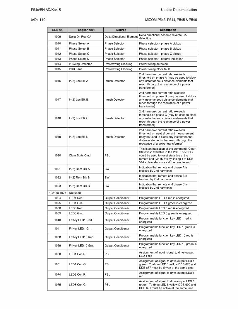
P54x/EN AD/Kb4-S Update Documentation
(AD) -110
MiCOM P543, P544, P545 & P546
DDB no. English text Source Description
1009 Delta Dir Rev CA Delta Directional Element Delta directional scheme reverse CA detection
1010 Phase Select A Phase Selector Phase selector - phase A pickup
1011 Phase Select B Phase Selector Phase selector - phase B pickup
1012 Phase Select C Phase Selector Phase selector - phase C pickup
1013 Phase Select N Phase Selector Phase selector - neutral indication
1014 P Swing Detector Powerswing Blocking Power swing detected
1015 PSB Fault Powerswing Blocking Power swing block fault
1016 Ih(2) Loc Blk A Inrush Detector
2nd harmonic current ratio exceeds threshold on phase A (may be used to block any instantaneous distance elements that reach through the reactance of a power transformer)
1017 Ih(2) Loc Blk B Inrush Detector
2nd harmonic current ratio exceeds threshold on phase B (may be used to block any instantaneous distance elements that reach through the reactance of a power transformer)
1018 Ih(2) Loc Blk C Inrush Detector
2nd harmonic current ratio exceeds threshold on phase C (may be used to block any instantaneous distance elements that reach through the reactance of a power transformer)
1019 Ih(2) Loc Blk N Inrush Detector
2nd harmonic current ratio exceeds threshold on neutral current measurement (may be used to block any instantaneous distance elements that reach through the reactance of a power transformer)
1020 Clear Stats Cmd PSL
This is an indication of the command “Clear Statistics” available in the PSL. This DDB could be used to reset statistics at the remote end (via IM64) by linking it to DDB 544 - clear statistics - at the remote end
1021 Ih(2) Rem Blk A SW Indication that remote end phase A is blocked by 2nd harmonic
1022 Ih(2) Rem Blk B SW Indication that remote end phase B is blocked by 2nd harmonic
1023 Ih(2) Rem Blk C SW Indication that remote end phase C is blocked by 2nd harmonic
1021 to 1023 Not used
1024 LED1 Red Output Conditioner Programmable LED 1 red is energized
1025 LED1 Grn. Output Conditioner Programmable LED 1 green is energized
1038 LED8 Red Output Conditioner Programmable LED 8 red is energized
1039 LED8 Grn. Output Conditioner Programmable LED 8 green is energized
1040 FnKey LED1 Red Output Conditioner Programmable function key LED 1 red is energized
1041 FnKey LED1 Grn. Output Conditioner Programmable function key LED 1 green is energized
1058 FnKey LED10 Red Output Conditioner Programmable function key LED 10 red is energized
1059 FnKey LED10 Grn. Output Conditioner Programmable function key LED 10 green is energized
1060 LED1 Con R PSL Assignment of input signal to drive output LED 1 red
1061 LED1 Con G PSL Assignment of signal to drive output LED 1 green. To drive LED 1 yellow DDB 676 and DDB 677 must be driven at the same time
1074 LED8 Con R PSL Assignment of signal to drive output LED 8 red
1075 LED8 Con G PSL Assignment of signal to drive output LED 8 green. To drive LED 8 yellow DDB 690 and DDB 691 must be active at the same time

Update Documentation P54x/EN AD/Kb4 MiCOM P543, P544, P545 & P546
(AD) -111
DDB no. English text Source Description
1076 FnKey LED1 ConR PSL Assignment of signal to drive output function key LED 1 red. This LED is associated with function key 1
1077 FnKey LED1 ConG PSL
Assignment of signal to drive output function key LED 1 green. This LED is associated with function key 1. To drive function key LED, yellow DDB 692 and DDB 693 must be active at the same time
1094 FnKey LED10 ConR PSL Assignment of signal to drive output function key LED 10 red. This LED is associated with function key 10
1095 FnKey LED10 ConG PSL
Assignment of signal to drive output function key LED 10 green. This LED is associated with function key 10. To drive function key LED1 yellow, DDB 710 and DDB 711 must be active at the same time
1096 Function Key 1 Function Key Function key 1 is activated. In ‘Normal’ mode it is high on keypress and in ‘Toggle’ mode remains high/low on single keypress
1105 Function Key 10 Function Key Function key 10 is activated. In ‘Normal’ mode it is high on keypress and in ‘Toggle’ mode remains high/low on single keypress
1106 I^ Maint. Alarm (CB1) CB Monitoring Broken current maintenance alarm - circuit breaker cumulative duty alarm set-point
1107 I^ Lockout Alarm (CB1) CB Monitoring Broken current lockout alarm - circuit breaker cumulative duty has been exceeded
1108 CB OPs Maint. (CB1) CB Monitoring No of circuit breaker operations maintenance alarm - indicated due to circuit breaker trip operations threshold
1109 CB OPs Lockout (CB1) CB Monitoring No of circuit breaker operations maintenance lockout - excessive number of circuit breaker trip operations, safety lockout
1110 CB Op Time Maint (CB1) CB Monitoring
Excessive circuit breaker operating time maintenance alarm - excessive operation time alarm for the circuit breaker (slow interruption time)
1111 CB Op Time Lockout (CB1) CB Monitoring
Excessive circuit breaker operating time lockout alarm - excessive operation time alarm for the circuit breaker (too slow interruption)
1112 Fault Freq. Lock (CB1) CB Monitoring Excessive fault frequency lockout alarm
1113 CB2 I^ Maint CB2 Monitoring Broken current maintenance alarm - circuit breaker cumulative duty alarm set-point CB2P544 and P546 only
1114 CB2 I^ Lockout CB2 Monitoring
Broken current lockout alarm - circuit breaker cumulative duty has been exceeded CB2 P544 and P546 only
1115 No.CB2 OPs Maint CB2 Monitoring
No of circuit breaker operations maintenance alarm - indicated due to circuit breaker trip operations threshold CB2 P544 and P546 only
1116 No.CB2 OPs Lock CB2 Monitoring
No of circuit breaker operations maintenance lockout - excessive number of circuit breaker trip operations, safety lockout CB2 P544 and P546 only
1117 CB2 Time Maint CB2 Monitoring
Excessive circuit breaker operating time maintenance alarm - excessive operation time alarm for the circuit breaker (slow interruption time) CB2 P544 and P546 only

P54x/EN AD/Kb4-S Update Documentation
(AD) -112
MiCOM P543, P544, P545 & P546
DDB no. English text Source Description
1118 CB2 Time Lockout CB2 Monitoring
Excessive circuit breaker operating time lockout alarm - excessive operation time alarm for the circuit breaker (too slow interruption) CB2 P544 and P546 only
1119 CB2FaultFreqLock CB2 Monitoring Excessive fault frequency lockout alarm CB2 P544 and P546 only
1120 SignalFail Ch1Rx C Diff Reception of messages on channel 1 has stopped
1121 SignalFail Ch1Tx C Diff Transmission of messages on channel 1 has stopped
1122 Ch 1 GPS Fail C Diff It indicates that GPS sampling synchronization (for protection purposes) running on channel 1 is lost
1123 Ch1 Mux Clk Fiber Monitor Bits This is an alarm that appears if the channel 1 baud rate is outside the limits 52 Kbis/s or70 Kbits/s
1124 Ch1 Signal Lost Fiber Monitor Bits Mux indicates signal lost over channel 1
1125 Ch1 Path Yellow Fiber Monitor Bits One way communication. Local relay that is sending over Ch1 indicates that remote end is not receiving
1126 Ch1 Mismatch RxN Fiber Monitor Bits Indication of mismatch between Ch1 N*64kbits/s setting and Mux
1127 Ch1 Timeout Fiber Monitor Bits Indication that no valid message is received over channel 1 during ‘Channel Timeout’ window
1128 Ch1 Degraded Fiber Monitor Bits Indicates poor channel 1 quality
1129 Ch1 Passthrough Fiber Monitor Bits Ch1 data received via Ch 2 in 3 ended configuration - self healing indication -
1130 SignalFail Ch2Rx C Diff Reception of messages on channel 2 has stopped
1131 SignalFail Ch2Tx C Diff Transmission of messages on channel 1 has stopped
1132 Ch 2 GPS Fail C Diff It indicates that GPS sampling synchronization (for protection purposes) running on channel 2 is lost
1133 Ch2 Mux Clk Fiber Monitor Bits This is an alarm that appears if the channel 2 baud rate is outside the limits 52Kbis/s or70 Kbits/s
1134 Ch2 Signal Lost Fiber Monitor Bits Mux indicates signal lost over channel 2
1135 Ch2 Path Yellow Fiber Monitor Bits One way communication. Local relay that is sending over Ch2 indicates that remote end is not receiving
1136 Ch2 Mismatch RxN Fiber Monitor Bits Indication of mismatch between InterMiCOM64 Ch 2 setting and Mux
1137 Ch2 Timeout Fiber Monitor Bits Indication that no valid message is received over channel 2 during ‘Channel Timeout’ window
1138 Ch2 Degraded Fiber Monitor Bits Indicates poor channel 2 quality
1139 Ch2 Passthrough Fiber Monitor Bits Ch2 data received via Ch 1 in 3 ended configuration - self healing indication -
1140 to 1148 Hidden
1149 F<1 Timer Block PSL Block Underfrequency Stage 1 Timer
1150 F<2 Timer Block PSL Block Underfrequency Stage 2 Timer
1151 F<3 Timer Block PSL Block Underfrequency Stage 3 Timer
1152 F<4 Timer Block PSL Block Underfrequency Stage 4 Timer
1153 F>1 Timer Block PSL Block Overfrequency Stage 1 Timer
1154 F>2 Timer Block PSL Block Overfrequency Stage 2 Timer
1155 F<1 Start Frequency Protection Underfrequency Stage 1 Start
1156 F<2 Start Frequency Protection Underfrequency Stage 2 Start
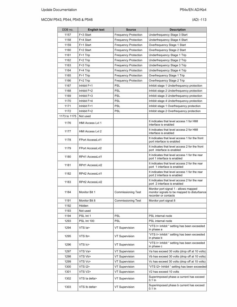
Update Documentation P54x/EN AD/Kb4 MiCOM P543, P544, P545 & P546
(AD) -113
DDB no. English text Source Description
1157 F<3 Start Frequency Protection Underfrequency Stage 3 Start
1158 F<4 Start Frequency Protection Underfrequency Stage 4 Start
1159 F>1 Start Frequency Protection Overfrequency Stage 1 Start
1160 F>2 Start Frequency Protection Overfrequency Stage 2 Start
1161 F<1 Trip Frequency Protection Underfrequency Stage 1 Trip
1162 F<2 Trip Frequency Protection Underfrequency Stage 2 Trip
1163 F<3 Trip Frequency Protection Underfrequency Stage 3 Trip
1164 F<4 Trip Frequency Protection Underfrequency Stage 4 Trip
1165 F>1 Trip Frequency Protection Overfrequency Stage 1 Trip
1166 F>2 Trip Frequency Protection Overfrequency Stage 2 Trip
1167 Inhibit F<1 PSL Inhibit stage 1 Underfrequency protection
1168 Inhibit F<2 PSL Inhibit stage 2 Underfrequency protection
1169 Inhibit F<3 PSL Inhibit stage 3 Underfrequency protection
1170 Inhibit F<4 PSL Inhibit stage 4 Underfrequency protection
1171 Inhibit F>1 PSL Inhibit stage 1 Overfrequency protection
1172 Inhibit F>2 PSL Inhibit stage 2 Overfrequency protection
1173 to 1175 Not used
1176 HMI Access Lvl 1 It indicates that level access 1 for HMI interface is enabled
1177 HMI Access Lvl 2 It indicates that level access 2 for HMI interface is enabled
1178 FPort AccessLvl1 It indicates that level access 1 for the front port interface is enabled
1179 FPort AccessLvl2 It indicates that level access 2 for the front port interface is enabled
1180 RPrt1 AccessLvl1 It indicates that level access 1 for the rear port 1 interface is enabled
1181 RPrt1 AccessLvl2 It indicates that level access 2 for the rear port 1 interface is enabled
1182 RPrt2 AccessLvl1 It indicates that level access 1 for the rear port 2 interface is enabled
1183 RPrt2 AccessLvl2 It indicates that level access 2 for the rear port 2 interface is enabled
1184 Monitor Bit 1 Commissioning Test Monitor port signal 1 - allows mapped monitor signals to be mapped to disturbance recorder or contacts
1191 Monitor Bit 8 Commissioning Test Monitor port signal 8
1192 Hidden
1193 Not used
1194 PSL Int 1 PSL PSL internal node
1293 PSL Int 100 PSL PSL internal node
1294 VTS Ia> VT Supervision “VTS I> Inhibit “ setting has been exceeded in phase a
1295 VTS Ib> VT Supervision “VTS I> Inhibit “ setting has been exceeded in phase b
1296 VTS Ic> VT Supervision “VTS I> Inhibit “ setting has been exceeded in phase c
1297 VTS Va> VT Supervision Va has exceed 30 volts (drop off at 10 volts)
1298 VTS Vb> VT Supervision Vb has exceed 30 volts (drop off at 10 volts)
1299 VTS Vc> VT Supervision Vc has exceed 30 volts (drop off at 10 volts)
1300 VTS I2> VT Supervision “VTS I2> Inhibit “ setting has been exceeded
1301 VTS V2> VT Supervision V2 has exceed 10 volts
1302 VTS Ia delta> VT Supervision Superimposed phase a current has exceed 0.1 In
1303 VTS Ib delta> VT Supervision Superimposed phase b current has exceed 0.1 In

P54x/EN AD/Kb4-S Update Documentation
(AD) -114
MiCOM P543, P544, P545 & P546
DDB no. English text Source Description
1304 VTS Ic delta> VT Supervision Superimposed phase c current has exceed 0.1 In
1305 to 1363 Not used
1364 CB1 Pre-Lockout Output from CB1 monitoring logic
1363 to 1374 Not used
1375 Teleprotection Disturbed This is an output signal available in the PSL, that could be mapped to “C Diff Failure” for IEC 870-5-103
1376 I>> Back Up Supervision
This applies only if distance primary FUN is selected (in IEC 870-5-103) This signal is ON if an overcurrent stage is selected to be enabled on VTS and distance is blocked by VTS
1377 O/C Trip By VTS
This applies only if distance primary FUN is selected (in IEC 870-5-103) This signal is ON if DDB 1376 is ON and one of the overcurrent stages set to be enabled on VTS condition trips
1378 Teleprot Tx
This applies only if distance primary FUN is selected (in IEC 870-5-103) This is an output signal available in the PSL, which could be mapped to a signal send of one of the two teleprotection channels
1379 Teleprot Rx
This applies only if distance primary FUN is selected (in IEC 870-5-103) This is an output signal available in the PSL, which could be mapped to a signal receive of one of the two teleprotection channels
1380 Group Warning
This is an output signal available in the PSL, which can be mapped in IEC 870-5-103 to a minor defect which does not shut down the main protection
1381 Group Alarm
This is an output signal available in the PSL, which can be mapped in IEC 870-5-103 to a major problem normally linked to the watchdog
1382 AR On Pulse This is an output signal available in the PSL, which can be mapped to enable AR via pulse
1383 AR OFF Pulse This is an output signal available in the PSL, which can be mapped to disable AR via pulse
1384 AR Enable This is an output signal available in the PSL, which can be mapped to enable AR
1385 AR In Service Auto-reclose in service
1386 MaxCh1 PropDelay Setting MaxCh 1 PropDelay has been exceeded
1387 MaxCh2 PropDelay Setting MaxCh 2 PropDelay has been exceeded
1388 MaxCh1 Tx-RxTime Setting MaxCh1 Tx-RxTime has been exceeded
1389 MaxCh2 Tx-RxTime Setting MaxCh2 Tx-RxTime has been exceeded
1390 to 1403 Not used
1404 VTS Blk Distance VTS Logic Signal from the VTS logic that can be used to block operation of the distance elements
1405 to 1407 Not used

Update Documentation P54x/EN AD/Kb4 MiCOM P543, P544, P545 & P546
(AD) -115
DDB no. English text Source Description
1408 CB2 Lead Auto-reclose
If setting "Leader Select By:" = Opto, then preferred leader CB is CB1 if input DDB "CB2 LEAD" is low, or CB2 if DDB "CB2 LEAD" is high. P544 and P546 only
1409 Follower AR 1P Auto-reclose
If setting "Foll AR Mode" = Opto, then if input DDB "FARSP" is high, the follower CB is enabled for single phase autoreclose, if "FARSP" is low, the follower CB is NOT enabled for single phase autoreclose.D2215P544 and P546 only
1410 Follower AR 3P Auto-reclose
If setting "Foll AR Mode" = Opto, then if input DDB "FAR3P" is high, the follower CB is enabled for three phase autoreclose, if "FAR3P" is low, the follower CB is NOT enabled for three phase autoreclose. P544 and P546 only
1411 CB2 AR 3p InProg Auto-reclose Autoreclose in progress CB2 P544 and P546 only
1412 En CB2 Independ Auto-reclose
DDB mapped in PSL from opto or comms input. A signal from an autoreclose scheme on an adjacent circuit having shared control of CB2, to allow the "Independent Follower time" to start. (see description for DDB "CB2 Indep Init A" or "CB2 Indep Init B" or "CB2 Indep Init C" ). P544 and P546 only
1413 to 1416 Not used
1417 Ext Rst CB2 AROK PSL
DDB mapped in PSL from opto or comms input. This input DDB is used when required to reset any CB2 Successful Autoreclose" signal. P544 and P546 only
1418 Ext Rst CB2Shots PSL
DDB mapped in PSL from opto or comms input. This input DDB is used when required to reset the CB2 cumulative "Shots" counters. P544 and P546 only
1419 Rst CB2 CloseDly PSL
DDB mapped in PSL. Reset Manual CB2 Close Timer Delay (stop & reset Manual Close Delay time for closing CB2). P544 and P546 only
1420 Inhibit AR PSL DDB mapped in PSL from opto or comms input. External signal to inhibit autoreclose.P544 and P546 only
1421 Block CB2 AR PSL
DDB mapped in PSL from opto or comms input. External signal to force CB2 autoreclose to lockout. P544 and P546 only
1422 Rst CB2 Lockout PSL
DDB mapped in PSL from opto or comms input. Reset Lockout Opto Input to reset CB2 Lockout state P544 and P546 only
1423 MCB/VTS CS2 PSL
DDB mapped in PSL from opto input (Bus2 VT secondary MCB tripped or VT fail detected by external VTS scheme), or signal from host relay VTS scheme P544 and P546 only
1424 Inhibit LB2 PSL
DDB mapped in PSL from opto input (external signal to inhibit Live Bus 2 function) P544 and P546 only

P54x/EN AD/Kb4-S Update Documentation
(AD) -116
MiCOM P543, P544, P545 & P546
DDB no. English text Source Description
1425 Inhibit DB2 PSL
DDB mapped in PSL from opto input (external signal to inhibit Dead Bus 2 function) P544 and P546 only
1426 CB2 CS1 Enabled PSL
DDB mapped in PSL from opto input or logic DDBs (enable CS2-1 check synchronism function) P544 and P546 only
1427 CB2 CS2 Enabled PSL
DDB mapped in PSL from opto input or logic DDBs (enable CS2-2 check synchronism function) P544 and P546 only
1428 CB2 In Service
Signal from CB In Service logic, indicating that CB2 is "In Service", i.e. can be initiated to autoreclose, P544 and P546 only
1429 CB2 NoAR Autoreclose CB2 not available for autoreclose P544 and P546 only
1430 Not used
1431 Leader CB2 Autoreclose CB2 set as leader P544 and P546 only
1432 Follower CB1 Autoreclose CB1 set as follower P544 and P546 only
1433 Follower CB2 Autoreclose CB2 set as follower P544 and P546 only
1434 CB2 AR Init Autoreclose Indicates initiation of a CB2 autoreclose cycle P544 and P546 only.
1435 CB2 ARIP Autoreclose CB2 autoreclose cycle in progress P544 and P546 only
1436 Not used
1437 Differential High Start C Diff Current differential High Set start
1438 Differential High Start A C Diff Current differential High Set A phase start
1439 Differential High Start B C Diff Current differential High Set B phase start
1440 Differential High Start C C Diff Current differential High Set C phase start
1441 CB2 Failed AR CB2 autoreclose failed due to persistent fault P544 and P546 only
1442 DTOK CB2L 1P
Output DDB indicates conditions to enable CB2 lead single phase autoreclose dead time to run are satisfied P544 and P546 only
1443 DTOK CB2L 3P
Output DDB indicates conditions to enable CB2 lead three phase autoreclose dead time to run are satisfied P544 and P546 only
1444 CB2 3P DTime Indicates CB2 three phase autoreclose dead time running P544 and P546 only
1445 En CB2 Follower Indicates conditions are satisfied to enable CB2 follower sequence P544 and P546 only
1446 1P Follower Time Indicates a single pole autoreclose follower time is running (either CB) P544 and P546 only
1447 3P Follower Time Indicates a three pole autoreclose follower time is running (either CB) P544 and P546 only

Update Documentation P54x/EN AD/Kb4 MiCOM P543, P544, P545 & P546
(AD) -117
DDB no. English text Source Description
1448 Auto Close CB2 Signal from autoreclose logic to initiate CB2 close via “CB2 CB Control” P544 and P546 only
1449 Set CB2 Close Indicates a CB2 Auto Close signal has been issued P544 and P546 only
1450 CB2 Control
Output DDB can be applied to inhibit CB2 reclose by adjacent scheme until local autoreclose scheme confirms it is OK to close CB2 P544 and P546 only
1451 CB2 Succ 1P AR CB2 successful single phase AR P544 and P546 only
1452 CB2 Succ 3P AR CB2 successful three phase AR P544 and P546 only
1453 CB2 Close inProg CB2 Manual Close initiated – awaiting Man Close Delay time P544 and P546 only
1454 CB2 Fast SCOK OK to reclose CB2 with sync check without waiting for dead time to complete P544 and P546 only
1455 CB2L SCOK System conditions OK to reclose CB2 as leader when dead time complete P544 and P546 only
1456 CB2F SCOK System conditions OK to reclose CB2 when follower time complete P544 and P546 only
1457 Not used
1458 CB2 Man SCOK System conditions OK to manually close CB2 P544 and P546 only
1459 CB2 Fail Pr Trip signal to force CB2 AR lockout if CB2 fails to trip when protection operates P544 and P546 only
1460 Not used
1461 Live Bus 2 Indicates Bus 2 input is live, i.e. voltage >= setting "Live Bus 2" P544 and P546 only
1462 Dead Bus 2 Indicates Bus 2 input is dead i.e. voltage < setting "Dead Bus 2" P544 and P546 only
1463 CB2 CS2 OK
CB2 close with synchronism check type 2 is permitted (setting CS2-2 = Enabled), and Line and Bus 2 voltages satisfy relay settings for CB2 synchronism check type 2 P544 and P546 only
1464 CB1 CS2 SlipF>
Line-Bus 1 slip freq > SlipFr 1-2 setting (frequency difference (slip) between line voltage and bus 1 voltage is greater than maximum slip permitted for CB1 synchronism check type 2) P544 and P546 only
1465 CB1 CS2 SlipF<
Line-Bus 1 slip freq < SlipFr 1-2 setting (frequency difference (slip) between line voltage and bus 1 voltage is within the permitted range for CB1 synchronism check type 2) P544 and P546 only

P54x/EN AD/Kb4-S Update Documentation
(AD) -118
MiCOM P543, P544, P545 & P546
DDB no. English text Source Description
1466 CB2 CS1 SlipF>
Line-Bus 2 slip freq > SlipFr 2-1 setting (frequency difference (slip) between line voltage and bus 2 voltage is greater than maximum slip permitted for CB2 synchronism check type 1) P544 and P546 only
1467 CB2 CS1 SlipF<
Line-Bus 2 slip freq < SlipFr 2-1 setting (frequency difference (slip) between line voltage and bus 2 voltage is within the permitted range for CB2 synchronism check type 1) P544 and P546 only
1468 CB2 CS2 SlipF>
Line-Bus 2 slip freq > SlipFr 2-2 setting (frequency difference (slip) between line voltage and bus 2 voltage is greater than maximum slip permitted for CB2 synchronism check type 2) P544 and P546 only
1469 CB2 CS2 SlipF<
Line-Bus 2 slip freq < SlipFr 2-2 setting (frequency difference (slip) between line voltage and bus 2 voltage is within the permitted range for CB2 synchronism check type 2) P544 and P546 only
1470 CB2 CS1 VL>VB
Voltage magnitude difference between Line V and Bus2 V is greater than setting "VDiff2-1" (line V > Bus V) P544 and P546 only
1471 CB2 CS2 VL>VB
Voltage magnitude difference between Line V and Bus2 V is greater than setting "VDiff2-1" (line V > Bus V) P544 and P546 only
1472 CB2 CS1 VL<VB
Voltage magnitude difference between Line V and Bus2 V is greater than setting "VDiff2-1" (line V < Bus V) P544 and P546 only
1473 CB2 CS2 VL<VB
Voltage magnitude difference between Line V and Bus2 V is greater than setting "VDiff2-1" (line V < Bus V) P544 and P546 only
1474 CB2 CS1 FL>FB
Frequency difference between Line V and Bus2 V is greater than setting "SlipFr2-1" (line freq > Bus freq) P544 and P546 only
1475 CB2 CS2 FL>FB Frequency difference between Line V and Bus2 V is greater than setting "SlipFr2-2" (line freq > Bus freq)+D2253
1476 CB2 CS1 FL<FB
Frequency difference between Line V and Bus2 V is greater than setting "SlipFr2-1" (line freq < Bus freq) P544 and P546 only
1477 CB2 CS2 FL<FB
Frequency difference between Line V and Bus2 V is greater than setting "SlipFr2-2" (line freq < Bus freq) P544 and P546 only
1478 CB2 CS1 AngHigh+ Line/Bus2 phase angle in range: +Angle 2-1 to +180deg (anticlockwise from Vbus) P544 and P546 only
1479 CB2 CS1 AngHigh- Line/Bus2 phase angle in range: -Angle 2-1 to -180deg (clockwise from Vbus) P544 and P546 only
1480 CB2 CS2 AngHigh+ Line/Bus2 phase angle in range: +Angle 2-2 to +180deg (anticlockwise from Vbus) P544 and P546 only

Update Documentation P54x/EN AD/Kb4 MiCOM P543, P544, P545 & P546
(AD) -119
DDB no. English text Source Description
1481 CB2 CS2 AngHigh- Line/Bus2 phase angle in range: -Angle 2-2 to -180deg (clockwise from Vbus) P544 and P546 only
1482 CB2 CS AngRotACW
Line freq > (Bus2 freq + 0.001 Hz) (Line voltage vector rotating anticlockwise relative to VBus2) P544 and P546 only
1483 CB2 CS AngRotCW
Bus2 freq > (Line freq + 0.001 Hz) (Line voltage vector rotating clockwise relative to VBus2) P544 and P546 only
1484 SChksInactiveCB2
Output from CB2 system check logic: indicates system checks for CB2 are disabled (setting "System Checks CB2" = Disabled or global setting "System Checks" = Disabled) P544 and P546 only
1485 AR Force CB2 3P Autoreclose
This DDB is set when the autoreclose logic has determined that single pole tripping/autoreclosing is not permitted for CB2. It can be applied in PSL when required to force trip conversion logic for internal and/or external protection to three phase trip mode for CB2. P544 and P546 only
1486 Not used
1487 Not used
1488 En CB1 Follower Indicates conditions are satisfied to enable CB1 follower sequence P544 and P546 only
1489 to 1492 Not used
1493 CB1 CS2 FL>FB
Frequency difference between Line V and Bus1 V is greater than setting "SlipFr1-2" (line freq > Bus freq) P544 and P546 only
1494 CB1 CS2 FL<FB
Frequency difference between Line V and Bus1 V is greater than setting "SlipFr1-2" (line freq < Bus freq) P544 and P546 only
1495 CB1 CS2 AngHigh+ Line/Bus1 phase angle in range: +Angle 1-2 to +180deg (anticlockwise from Vbus) P544 and P546 only
1496 CB1 CS2 AngHigh- Line/Bus1 phase angle in range: -Angle 1-2 to -180deg (clockwise from Vbus) P544 and P546 only
1497 Lead AR 1P PSL
If setting "Lead AR Mode" = Opto, then if input DDB "LARSP" is high, the leader CB is enabled for single phase autoreclose, if "LARSP" is low, the leader CB is NOT enabled for single phase autoreclose. P544 and P546 only
1498 Lead AR 3P PSL
If setting "Lead AR Mode" = Opto, then if input DDB "LAR3P" is high, the leader CB is enabled for three phase autoreclose, if "LAR3P" is low, the leader CB is NOT enabled for three phase autoreclose. P544 and P546 only
1499 CB2 Trip AR MemA CB2 A Ph trip & AR initiation memory P544 and P546 only
1500 CB2 Trip AR MemB CB2 B Ph trip & AR initiation memory P544 and P546 only

P54x/EN AD/Kb4-S Update Documentation
(AD) -120
MiCOM P543, P544, P545 & P546
DDB no. English text Source Description
1501 CB2 Trip AR MemC CB2 C Ph trip & AR initiation memory P544 and P546 only
1502 to 1503 Not used
1504 Init APh AR Test PSL
DDB mapped in PSL from opto or comms input. Input high-low operation will initiate APh test trip & autoreclose cycle P544 and P546 only
1505 Init BPh AR Test PSL
DDB mapped in PSL from opto or comms input. Input high-low operation will initiate BPh test trip & autoreclose cycle P544 and P546 only
1506 Init CPh AR Test PSL
DDB mapped in PSL from opto or comms input. Input high-low operation will initiate CPh test trip & autoreclose cycle P544 and P546 only
1507 Init 3P AR Test PSL
DDB mapped in PSL from opto or comms input. Input high-low operation will initiate 3Ph test trip & autoreclose cycle P544 and P546 only
1508 Ext Fault APh PSL
DDB mapped in PSL from opto or comms input: indicates external protection operated for fault involving A phase P544 and P546 only
1509 Ext Fault BPh PSL
DDB mapped in PSL from opto or comms input: indicates external protection operated for fault involving B phase P544 and P546 only
1510 Ext Fault CPh PSL
DDB mapped in PSL from opto or comms input: indicates external protection operated for fault involving C phase P544 and P546 only
1511 to 1516 Not used
1517 Ext Rst CB1 AROK PSL
DDB mapped in PSL from opto or comms input. This input DDB is used when required to reset any CB1 "Successful Autoreclose" signal. P544 and P546 only
1518 Ext Rst CB1Shots PSL
DDB mapped in PSL from opto or comms input. This input DDB is used when required to reset the CB1 cumulative "Shots" counters. P544 and P546 only
1519 to 1520 Not used
1521 MCB/VTS CS1 PSL
DDB mapped in PSL from opto input (Bus1 VT secondary MCB tripped or VT fail detected by external VTS scheme), or signal from host relay VTS scheme P544 and P546 only
1522 Inhibit LL PSL DDB mapped in PSL from opto input (external signal to inhibit Live Line function) P544 and P546 only
1523 Inhibit DL PSL DDB mapped in PSL from opto input (external signal to inhibit Dead Line function)P544 and P546 only
1524 Inhibit LB1 PSL
DDB mapped in PSL from opto input (external signal to inhibit Live Bus 1 function) P544 and P546 only
1525 Inhibit DB1 PSL
DDB mapped in PSL from opto input (external signal to inhibit Dead Bus 1 function) P544 and P546 only

Update Documentation P54x/EN AD/Kb4 MiCOM P543, P544, P545 & P546
(AD) -121
DDB no. English text Source Description
1526 CB1 In Service CB1 In Service (can be initiated for autoreclose) P544 and P546 only
1527 Not used
1528 CB1 NoAR Autoreclose CB1 not available for autoreclose P544 and P546 only
1529 Not used
1530 Leader CB1 Autoreclose CB1 set as leader P544 and P546 only
1531 to 1534 Not used
1535 CB1 Trip AR MemA A Ph trip & AR initiation memory P544 and P546 only
1536 CB1 Trip AR MemB B Ph trip & AR initiation memory P544 and P546 only
1537 CB1 Trip AR MemC C Ph trip & AR initiation memory P544 and P546 only
1538 to 1540 Not used
1541 AR Start Autoreclose Any AR initiation signal present P544 and P546 only
1542 ARIP Autoreclose Any AR cycle in progress P544 and P546 only
1543 CB1 AR Init Autoreclose CB1 AR cycle initiation P544 and P546 only
1544 CB1 ARIP Autoreclose CB1 AR cycle in progress P544 and P546 only
1545 Not used
1546 SC Count>Shots Sequence counts greater than shots P544 and P546 only
1547 Evolve 3Ph
Convert SPAR to 3PAR. DDB mapped to give 100ms pulse to CB1 Trip 3Ph and CB2 Trip 3Ph outputs P544 and P546 only
1548 to 1549 Not used
1550 CB1 Failed AR CB1 AR failed due to persistent fault P544 and P546 only
1551 DTOK All Enabling condition for any dead time P544 and P546 only
1552 DTOK CB1L 1P required for CB1 lead SPAR D Time P544 and P546 only
1553 DTOK CB1L 3P required for CB1 lead 3PAR D Time P544 and P546 only
1554 1P DTime Single pole dead time in progress P544 and P546 only
1555 OK Time 3P OK to start 3PAR dead time P544 and P546 only
1556 3P DTime1 3Phase dead time 1 running P544 and P546 only
1557 3P DTime2 3Phase dead time 2 running P544 and P546 only
1558 3P DTime3 3Phase dead time 3 running P544 and P546 only
1559 3P DTime4 3Phase dead time 4 running P544 and P546 only

P54x/EN AD/Kb4-S Update Documentation
(AD) -122
MiCOM P543, P544, P545 & P546
DDB no. English text Source Description
1560 CB1 3P DTime CB1 3PAR dead time running P544 and P546 only
1561 1PF TComp Either CB SP follower time complete P544 and P546 only
1562 3PF TComp Either CB 3P follower time complete P544 and P546 only
1563 Indep 1PF TComp Either CB independent SP follower time complete P544 and P546 only
1564 Indep 3PF TComp Either CB independent 3P follower time complete P544 and P546 only
1565 Set CB1 Close DDB (Optional PSL mapping to indication) P544 and P546 only
1566 CB1 Control Inhibits CB1 reclose by adjacent scheme P544 and P546 only
1567 1P Reclaim Time Single Ph AR reclaim time running P544 and P546 only
1568 1P Reclaim TComp Single Ph AR reclaim time complete P544 and P546 only
1569 3P Reclaim Time Three Ph AR reclaim time running P544 and P546 only
1570 3P Reclaim TComp Three Ph AR reclaim time complete P544 and P546 only
1571 CB1 Succ 1P AR CB1 successful single phase AR P544 and P546 only
1572 CB1 Fast SCOK OK to reclose CB1 with sync check without waiting for dead time to complete P544 and P546 only
1573 CB1L SCOK System conditions OK to reclose CB1 when dead time complete P544 and P546 only
1574 CB1 Man SCOK System conditions OK to manually close CB1 P544 and P546 only
1575 CB1 Fail Pr Trip signal to force CB1 AR lockout P544 and P546 only
1576 Not used
1577 CB2 CS1 OK CS2-1 is enabled and Line and Bus 2 voltages meet CS2-1 settings P544 and P546 only
1578 CB1 CS1 SlipF> Line-Bus 1 slip freq > SlipFr 1-1 setting P544 and P546 only
1579 CB1 CS1 SlipF< Line-Bus 1 slip freq < SlipFr 1-1 setting P544 and P546 only
1580 CS VLine< Line Volts < CS UV setting P544 and P546 only
1581 CS VLine> Line Volts > CS OV setting P544 and P546 only
1582 CS VBus1< Bus1 Volts < CS UV setting P544 and P546 only
1583 CS VBus1> Bus1 Volts > CS OV setting P544 and P546 only
1584 CS VBus2< Bus2 Volts < CS UV setting P544 and P546 only
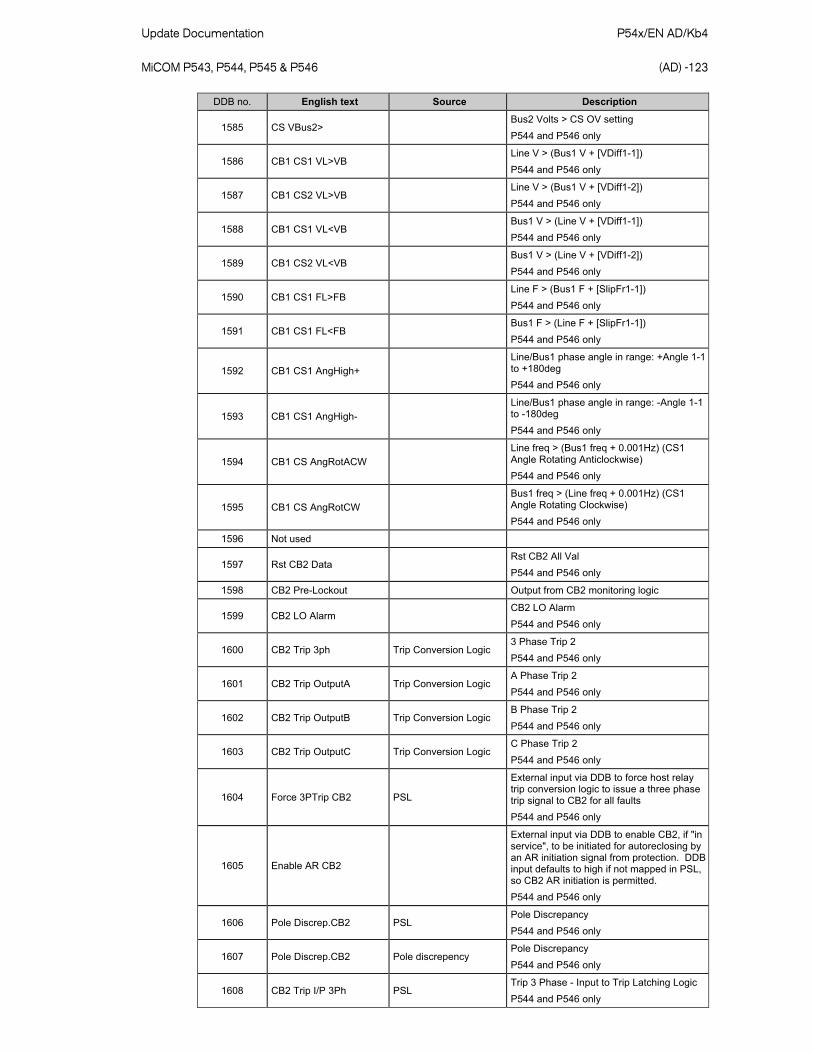
Update Documentation P54x/EN AD/Kb4 MiCOM P543, P544, P545 & P546
(AD) -123
DDB no. English text Source Description
1585 CS VBus2> Bus2 Volts > CS OV setting P544 and P546 only
1586 CB1 CS1 VL>VB Line V > (Bus1 V + [VDiff1-1]) P544 and P546 only
1587 CB1 CS2 VL>VB Line V > (Bus1 V + [VDiff1-2]) P544 and P546 only
1588 CB1 CS1 VL<VB Bus1 V > (Line V + [VDiff1-1]) P544 and P546 only
1589 CB1 CS2 VL<VB Bus1 V > (Line V + [VDiff1-2]) P544 and P546 only
1590 CB1 CS1 FL>FB Line F > (Bus1 F + [SlipFr1-1]) P544 and P546 only
1591 CB1 CS1 FL<FB Bus1 F > (Line F + [SlipFr1-1]) P544 and P546 only
1592 CB1 CS1 AngHigh+ Line/Bus1 phase angle in range: +Angle 1-1 to +180deg P544 and P546 only
1593 CB1 CS1 AngHigh- Line/Bus1 phase angle in range: -Angle 1-1 to -180deg P544 and P546 only
1594 CB1 CS AngRotACW Line freq > (Bus1 freq + 0.001Hz) (CS1 Angle Rotating Anticlockwise) P544 and P546 only
1595 CB1 CS AngRotCW Bus1 freq > (Line freq + 0.001Hz) (CS1 Angle Rotating Clockwise) P544 and P546 only
1596 Not used
1597 Rst CB2 Data Rst CB2 All Val P544 and P546 only
1598 CB2 Pre-Lockout Output from CB2 monitoring logic
1599 CB2 LO Alarm CB2 LO Alarm P544 and P546 only
1600 CB2 Trip 3ph Trip Conversion Logic 3 Phase Trip 2 P544 and P546 only
1601 CB2 Trip OutputA Trip Conversion Logic A Phase Trip 2 P544 and P546 only
1602 CB2 Trip OutputB Trip Conversion Logic B Phase Trip 2 P544 and P546 only
1603 CB2 Trip OutputC Trip Conversion Logic C Phase Trip 2 P544 and P546 only
1604 Force 3PTrip CB2 PSL
External input via DDB to force host relay trip conversion logic to issue a three phase trip signal to CB2 for all faults P544 and P546 only
1605 Enable AR CB2
External input via DDB to enable CB2, if "in service", to be initiated for autoreclosing by an AR initiation signal from protection. DDB input defaults to high if not mapped in PSL, so CB2 AR initiation is permitted. P544 and P546 only
1606 Pole Discrep.CB2 PSL Pole Discrepancy P544 and P546 only
1607 Pole Discrep.CB2 Pole discrepency Pole Discrepancy P544 and P546 only
1608 CB2 Trip I/P 3Ph PSL Trip 3 Phase - Input to Trip Latching Logic P544 and P546 only
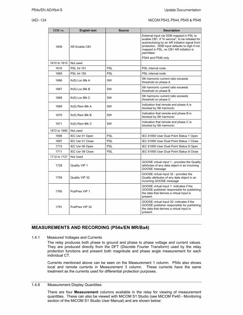
P54x/EN AD/Kb4-S Update Documentation
(AD) -124
MiCOM P543, P544, P545 & P546
DDB no. English text Source Description
1609 AR Enable CB1
External input via DDB mapped in PSL to enable CB1, if "in service", to be initiated for autoreclosing by an AR initiation signal from protection. DDB input defaults to high if not mapped in PSL, so CB1 AR initiation is permitted. P544 and P546 only
1610 to 1615 Not used
1616 PSL Int 101 PSL PSL internal node
1665 PSL Int 150 PSL PSL internal node
1666 Ih(5) Loc Blk A SW 5th harmonic current ratio exceeds threshold on phase A
1667 Ih(5) Loc Blk B SW 5th harmonic current ratio exceeds threshold on phase B
1668 Ih(5) Loc Blk C SW 5th harmonic current ratio exceeds threshold on phase C
1669 Ih(5) Rem Blk A SW Indication that remote end phase A is blocked by 5th harmonic
1670 Ih(5) Rem Blk B SW Indication that remote end phase B is blocked by 5th harmonic
1671 Ih(5) Rem Blk C SW Indication that remote end phase C is blocked by 5th harmonic
1672 to 1695 Not used
1696 IEC Usr 01 Open PSL IEC 61850 User Dual Point Status 1 Open
1697 IEC Usr 01 Close PSL IEC 61850 User Dual Point Status 1 Close
1710 IEC Usr 08 Open PSL IEC 61850 User Dual Point Status 8 Open
1711 IEC Usr 08 Close PSL IEC 61850 User Dual Point Status 8 Close
1712 to 1727 Not Used
1728 Quality VIP 1 GOOSE virtual input 1 - provides the Quality attributes of any data object in an incoming GOOSE message
1759 Quality VIP 32 GOOSE virtual input 32 - provides the Quality attributes of any data object in an incoming GOOSE message
1760 PubPres VIP 1
GOOSE virtual input 1- indicates if the GOOSE publisher responsible for publishing the data that derives a virtual input is present.
1791 PubPres VIP 32
GOOSE virtual input 32- indicates if the GOOSE publisher responsible for publishing the data that derives a virtual input is present.
MEASUREMENTS AND RECORDING (P54x/EN MR/Ba4)
1.4.1 Measured Voltages and Currents The relay produces both phase to ground and phase to phase voltage and current values. They are produced directly from the DFT (Discrete Fourier Transform) used by the relay protection functions and present both magnitude and phase angle measurement for each individual CT.
Currents mentioned above can be seen on the Measurement 1 column. P54x also shows local and remote currents in Measurement 3 column. These currents have the same treatment as the currents used for differential protection purposes.
1.4.8 Measurement Display Quantities
There are four Measurement columns available in the relay for viewing of measurement quantities. These can also be viewed with MiCOM S1 Studio (see MiCOM Px40 - Monitoring section of the MiCOM S1 Studio User Manual) and are shown below:

Update Documentation P54x/EN AD/Kb4 MiCOM P543, P544, P545 & P546
(AD) -125
MEASUREMENTS 1 MEASUREMENTS 2 MEASUREMENTS 3 MEASUREMENTS 4
IA Magnitude 0 A A Phase Watts 0 W IA Local 0 A Ch 1 Prop Delay
IA Phase Angle 0 deg B Phase Watts 0 W IA Angle Local 0 deg Ch 2 Prop Delay
IB Magnitude 0 A C Phase Watts 0 W IB Local 0 A Ch1 Rx Prop Delay
IB Phase Angle 0 deg A Phase VArs 0 Var IB Angle Local 0 deg Ch1 Tx Prop Delay
IC Magnitude 0 A B Phase VArs 0 Var IC Local 0 A Ch2 Rx Prop Delay
IC Phase Angle 0 deg C Phase VArs 0 Var IC Angle Local 0 deg Ch2 Tx Prop Delay
IN Derived Mag. 0 A A Phase VA 0 VA IA remote 1 0 A Channel 1 Status
IN Derived Angle 0 deg B Phase VA 0 VA IA Ang remote 1 0 deg Channel 2 Status
ISEF Magnitude 0 A C Phase VA 0 VA IB remote 1 0 A IM64 Rx Status
ISEF Angle 0 deg 3 Phase Watts 0 W IB Ang remote 1 0 deg STATISTICS
I1 Magnitude 0 A 3 Phase VArs 0 VAr IC remote 1 0 A Last Reset on
I2 Magnitude 0 A 3 Phase VA 0 VA IC Ang remote 1 0 deg Date/Time
I0 Magnitude 0 A 3Ph Power Factor 0 IA remote 2 0 A Ch1 No.Vald Mess
IA RMS 0 A APh Power Factor 0 IA Ang remote 2 0 deg Ch1 No.Err Mess
IB RMS 0 A BPh Power Factor 0 IB remote 2 0 A Ch1 No.Errored s
IC RMS 0 A CPh Power Factor 0 IB Ang remote 2 0 deg Ch1 No.Sev Err s
IN RMS 0 A 3Ph WHours Fwd 0 Wh IC remote 2 0 A Ch1 No. Dgraded m
VAB Magnitude 0 V 3Ph WHours Rev 0 Wh IC Ang remote 2 0 deg Ch2 No.Vald Mess
VAB Phase Angle 0 deg 3Ph VArHours Fwd 0 VArh IA Differential 0 A Ch2 No.Err Mess
VBC Magnitude 0 V 3Ph VArHours Rev 0 VArh IB Differential 0 A Ch2 No.Errored s
VBC Phase Angle 0 deg 3Ph W Fix Demand 0 W IC Differential 0 A Ch2 No.Sev Err s
VCA Magnitude 0 V 3Ph VArs Fix Dem. 0 VAr IA Bias 0 A Ch2 No. Dgraded m
VCA Phase Angle 0 deg IA Fixed Demand 0 A IB Bias 0 A Max Ch 1 Prop Delay
VAN Magnitude 0 V IB Fixed Demand 0 A IC Bias 0 A Max Ch 2 Prop Delay
VAN Phase Angle 0 deg IC Fixed Demand 0 A Max Ch1 TxRx Time
VBN Magnitude 0 V 3 Ph W Roll Dem. 0 W Max Ch2 TxRx Time
VBN Phase Angle 0 deg 3Ph VArs Roll Dem. 0 VAr Clear Statistics
VCN Magnitude 0 V IA Roll Demand 0 A
VCN Phase Angle 0 deg IB Roll Demand 0 A
IC Roll Demand 0 A
3Ph W Peak Dem. 0 W
V1 Magnitude 0 V 3Ph VAr Peak Dem. 0 VAr
V2 Magnitude 0 V IA Peak Demand 0 A
V0 Magnitude 0 V IB Peak Demand 0 A
VAN RMS 0 V IC Peak Demand 0 A
VBN RMS 0 V Reset Demand No
VCN RMS 0 V
VAB RMS 0 V
VBC RMS 0 V
VCA RMS 0 V
Frequency
CB1 CS Volt Mag 0 V
CB1 CS Volt Ang 0 deg
CB1 Bus-Line Ang 0 deg
CB1 CS Slip Freq
IM Magnitude 0 A
IM Phase Angle 0 deg
I1 Magnitude 0 A

P54x/EN AD/Kb4-S Update Documentation
(AD) -126
MiCOM P543, P544, P545 & P546
MEASUREMENTS 1 MEASUREMENTS 2 MEASUREMENTS 3 MEASUREMENTS 4
I1 Phase Angle 0 deg
I2 Magnitude 0 A
I2 Phase Angle 0 deg
I0 Magnitude 0 A
I0 Phase Angle 0 deg
V1 Magnitude 0 V
V1 Phase Angle 0 deg
V2 Magnitude 0 V
V2 Phase Angle 0 deg
V0 Magnitude 0 V
V0 Phase Angle 0 deg
CB2 CS Volt Mag 0 V
CB2 CS Volt Ang 0 deg
CB2 Bus-Line Ang 0 deg
CB2 CS Slip Freq
VRem Magnitude 0 V
VRem Phase Ang 0 deg
IA CT1 Magnitude 0 A
IA CT1 Phase Ang 0 deg
IB CT1 Magnitude 0 A
IB CT1 Phase Ang 0 deg
IC CT1 Magnitude 0 A
IC CT1 Phase Ang 0 deg
IA CT2 Magnitude 0 A
IA CT2 Phase Ang 0 deg
IB CT2 Magnitude 0 A
IB CT2 Phase Ang 0 deg
IC CT2 Magnitude 0 A
IC CT2 Phase Ang 0 deg
FIRMWARE AND SERVICE MANUAL VERSION HISTORY (P54x/EN VH/I84)


Firmware and Service Manual P54x/EN VH/Kb4-S Version History MiCOM P543, P544, P545 & P546 (VH) 16-126
Rel
ay ty
pe: P
54x
…
Softw
are
vers
ion
Har
dwar
e su
ffix
Orig
inal
da
te o
f iss
ue
Des
crip
tion
of c
hang
es
S1
co
mpa
tibili
ty
Tech
nica
l do
cum
enta
tion
Maj
or
Min
or
01
A
A
Fe
b 20
00
Firs
t rel
ease
to p
rodu
ctio
n V
1.07
or L
ater
TG
8613
A
02
A
A
Mar
200
0
�
PS
B.
Thre
e se
tting
s ad
ded
to s
et z
one
6 to
incr
ease
flexi
bilit
y �
P
rote
ctio
n ad
dres
s. U
nive
rsal
add
ress
add
ed
�
SE
F &
EF.
Pol
ariz
ing
volta
ge s
ettin
g ra
nge
incr
ease
d �
Th
erm
al.
Set
ting
rang
e in
crea
sed
�
Trip
con
vers
ion
logi
c. 3
DD
B s
igna
ls a
dded
to s
impl
ify lo
gic
for
us
ers
�
Dis
tanc
e. M
in p
olar
izin
g vo
ltage
incr
ease
d to
pre
vent
trip
ping
for c
lose
up
thre
e ph
ase
faul
ts
�
Che
ck s
ync.
ang
le m
easu
rem
ent i
mpr
oved
�
P
SB
. Te
xt fo
r pow
er s
win
g in
dica
tion
impr
oved
�
In
clud
e po
le d
iscr
epan
cy lo
gic
to P
543
�
Sus
cept
ance
set
ting
corre
cted
V1.
08 o
r Lat
er
TG86
13B
03
A
A
May
200
0
�
Ger
man
text
cha
nged
�
S
pani
sh te
xt c
hang
ed
�
Cha
nges
to D
DB
nam
es &
pro
perti
es
�
Impr
ovem
ents
in a
uto-
recl
ose
and
rese
t fro
m lo
ckou
t cod
e �
C
hang
es to
pol
e de
ad &
trip
con
vers
ion
logi
c �
C
hang
es to
P54
4 ci
rcui
t bre
aker
fail
logi
c �
A
dded
DD
B fo
r CS
103
test
mod
e �
R
ecom
men
d up
grad
ing
to 0
3B s
oftw
are
or la
ter
V1.
09 o
r Lat
er
TG86
13B

P54x/EN VH/Kb4-S Firmware and Service Manual Version History (VH) 16-127 MiCOM P543, P544, P545 & P546
Rel
ay ty
pe: P
54x
…
Softw
are
vers
ion
Har
dwar
e su
ffix
Orig
inal
da
te o
f iss
ue
Des
crip
tion
of c
hang
es
S1
co
mpa
tibili
ty
Tech
nica
l do
cum
enta
tion
Maj
or
Min
or
03 C
ont.
B
A
Feb
2002
�
All
build
s re
leas
ed fo
r mai
nten
ance
upg
rade
s �
R
esol
ved
poss
ible
rebo
ot c
ause
d by
dis
turb
ance
reco
rder
�
R
esol
ved
poss
ible
rebo
ot c
ause
d by
inva
lid M
OD
BU
S re
ques
ts�
R
esol
ved
a lo
ss o
f mea
sure
men
ts (c
olum
n 3
& 4
) pro
blem
that
ca
n oc
cur i
n 3
term
inal
app
licat
ions
�
Pr
oble
m w
here
by M
iCO
M S
1 co
uld
only
set
gro
up 1
line
leng
th
corre
cted
�
Fi
xed
capa
citiv
e ch
argi
ng c
urre
nt c
ompe
nsat
ion
in P
544
�
Cor
rect
ed P
544
disp
lay
of p
hase
C c
urre
nt p
hase
ang
le
�
IDM
T cu
rves
impr
ovem
ents
�
R
emov
ed ro
undi
ng e
rror i
n ca
lcul
atio
n of
tp
�
Men
u de
pend
ence
usi
ng ri
pple
bit
corre
cted
�
D
irect
iona
l/non
-dire
ctio
n ea
rth fa
ult f
ixed
�
B
atte
ry fa
il al
arm
impr
ovem
ents
�
P
ower
mea
sure
men
ts re
ad o
ver M
OD
BU
S m
ay b
e in
corr
ect
�
Res
olve
d pr
oble
m c
ause
d by
rapi
d ch
angi
ng s
elf r
eset
ting
alar
m re
setti
ng th
e re
lay
whe
n re
ad k
ey p
ress
ed
�
Pre
vent
ed s
oftw
are
erro
rs fr
om c
lear
ing
even
t log
V1.
09 o
r Lat
er
TG86
13B
A A
Aug
2000
�
Tr
ip c
onve
rsio
n lo
gic
mov
ed fr
om in
tern
al fi
xed
logi
c to
PS
L V
1.10
or L
ater
TG
8613
B
B
A
Mar
200
1 O
nly
P54
3 C
S10
3 bu
ilds
rele
ased
�
Im
prov
emen
ts to
the
CS
103
time
sync
hron
izat
ion
V1.
10 o
r Lat
er
TG86
13B
C
A Ju
n 20
01
Onl
y P
543
CS
103
build
s re
leas
ed.
Bas
ed o
n 04
B
�
Res
olve
d a
loss
of m
easu
rem
ents
(col
umns
3 &
4) p
robl
em
th
at c
an o
ccur
in 3
term
inal
app
licat
ions
V
1.10
or L
ater
TG
8613
B
04
D
A Ju
n 20
01
Onl
y P
543
CS
103
build
rele
ased
. B
ased
on
04C
�
P
reve
nts
a re
boot
on
pow
er-u
p w
hen
batte
ry is
rem
oved
V
1.10
or L
ater
TG
8613
B

Firmware and Service Manual P54x/EN VH/Kb4-S Version History MiCOM P543, P544, P545 & P546 (VH) 16-128
Rel
ay ty
pe: P
54x
…
Softw
are
vers
ion
Har
dwar
e su
ffix
Orig
inal
da
te o
f iss
ue
Des
crip
tion
of c
hang
es
S1
co
mpa
tibili
ty
Tech
nica
l do
cum
enta
tion
Maj
or
Min
or
A A
Sep
2000
Inte
rnal
rele
ase
for v
alid
atio
n on
ly
�
Incl
udes
DN
P3.
0 �
C
ourie
r bay
mod
ule
com
patib
ility
mod
ifica
tion
�
MO
DBU
S ba
y m
odul
e co
mpa
tibilit
y m
odifi
catio
n �
D
ista
nce
- Z3
sele
ctab
le fo
rwar
d/re
vers
e �
S
pani
sh te
xt c
orre
cted
�
M
enu
depe
nden
ce u
sing
ripp
le b
it co
rrect
ed
�
MO
DB
US
pro
blem
read
ing
nega
tive
valu
es o
f fau
lt lo
catio
n co
rrect
ed
�
RD
F fil
e m
odifi
ed
�
Dire
ctio
nal/n
on-d
irect
ion
earth
faul
t fix
ed
�
Bat
tery
fail
alar
m c
orre
cted
�
V
ery
low
faul
t loc
atio
n co
uld
be s
how
n in
corr
ectly
as
nega
tive
�
Som
e M
OD
BU
S a
ddre
ss c
hang
ed
V2.
0 or
Lat
er
TG86
13B
B
A
Oct
200
0
Rel
ease
d to
pro
duct
ion
�
Incl
udes
all
of 0
5A c
hang
es
�
Req
uire
men
t to
use
rela
ys 8
, 9 &
10
for T
rip A
, B &
C re
mov
ed�
M
OD
BU
S c
omm
unic
atio
n pr
oble
m w
hen
used
with
P14
0 fix
ed
�
Pow
er m
easu
rem
ents
read
ove
r MO
DB
US
may
be
inco
rrec
t �
M
OD
BU
S s
tatu
s re
gist
er re
ports
dis
turb
ance
reco
rds
inco
rrect
ly fo
llow
ing
pow
er c
ycle
V2.
0 or
Lat
er
TG86
13B
C
A
Mar
200
1 O
nly
P54
3 &
P54
4 bu
ilds
rele
ased
for c
usto
mer
test
s �
P
SB
now
wor
ks w
ith s
ingl
e po
le o
pen
V2.
0 or
Lat
er
TG86
13B
05
D
A
May
200
1
Onl
y P
543
& P
544
build
s re
leas
ed fo
r cus
tom
er te
sts
�
Dis
tanc
e di
rect
iona
l lin
e fix
ed a
t -30
º �
P
SB
blo
ck is
sued
whe
n im
peda
nce
pass
es in
to a
ny Z
1, Z
2 or
Z3
�
P
SB
unb
lock
via
neg
ativ
e se
quen
ce c
urre
nt n
ow d
one
via
PS
L
New
PSL
will
be
requ
ired
-

P54x/EN VH/Kb4-S Firmware and Service Manual Version History (VH) 16-129 MiCOM P543, P544, P545 & P546
Rel
ay ty
pe: P
54x
…
Softw
are
vers
ion
Har
dwar
e su
ffix
Orig
inal
da
te o
f iss
ue
Des
crip
tion
of c
hang
es
S1
co
mpa
tibili
ty
Tech
nica
l do
cum
enta
tion
Maj
or
Min
or
E A
Jun
2001
All
build
s re
leas
ed to
pro
duct
ion.
Bas
ed o
n 05
B s
oftw
are
�
Res
olve
d a
loss
of m
easu
rem
ents
(col
umn
3 &
4) p
robl
em th
at
can
occu
r in
3 te
rmin
al a
pplic
atio
ns
�
Rec
omm
ende
d up
grad
ing
to 0
5K o
r lat
er
V2.
0 or
Lat
er
TG86
13B
F A
S
ep 2
001
All
build
s re
leas
ed to
pro
duct
ion.
Bas
ed o
n 05
E s
oftw
are
�
Prob
lem
whe
reby
MiC
OM
S1
coul
d on
ly s
et g
roup
1 li
ne le
ngth
co
rrect
ed
�
Fixe
d ca
paci
tive
char
ging
cur
rent
com
pens
atio
n in
P54
4 �
C
orre
cted
P54
4 di
spla
y of
pha
se C
cur
rent
pha
se a
ngle
�
ID
MT
curv
es im
prov
emen
ts
�
Rem
oved
roun
ding
erro
r in
calc
ulat
ion
of tp
�
Fi
xed
prob
lem
s ca
used
by
chan
ges
to D
NP
3.0
addr
ess
�
Rec
omm
ende
d up
grad
ing
to 0
5K o
r lat
er
V2.
0 or
Lat
er
TG86
13B
G
A
Jan
2002
All
build
s ex
cept
MO
DB
US
rele
ased
to p
rodu
ctio
n. B
ased
on
05F
softw
are
�
Res
olve
d po
ssib
le re
boot
cau
sed
by d
istu
rban
ce re
cord
er
�
Pro
blem
in M
OD
BU
S b
uild
whi
ch c
an c
ause
a re
boot
�
R
ecom
men
ded
upgr
adin
g to
05K
or l
ater
V2.
0 or
Lat
er
TG86
13B
H
A Ja
n 20
02
All
build
s re
leas
ed to
pro
duct
ion.
Bas
ed o
n 05
G s
oftw
are
�
Res
olve
d po
ssib
le re
boot
cau
sed
by in
valid
MO
DB
US
requ
ests
�
Rec
omm
ende
d up
grad
ing
to 0
5K o
r lat
er
V2.
0 or
Lat
er
TG86
13B
05 C
ont.
I A
O
ct 2
002
Lim
ited
rele
ase
- not
rele
ased
to p
rodu
ctio
n. B
ased
on
05H
so
ftwar
e �
C
orre
ct th
e fo
rmat
use
d to
dis
play
freq
uenc
y ov
er th
e M
OD
BU
S in
terfa
ce
�
Rec
omm
ende
d up
grad
ing
to 0
5K o
r lat
er
V2.
0 or
Lat
er
TG86
13B

Firmware and Service Manual P54x/EN VH/Kb4-S Version History MiCOM P543, P544, P545 & P546 (VH) 16-130
Rel
ay ty
pe: P
54x
…
Softw
are
vers
ion
Har
dwar
e su
ffix
Orig
inal
da
te o
f iss
ue
Des
crip
tion
of c
hang
es
S1
co
mpa
tibili
ty
Tech
nica
l do
cum
enta
tion
Maj
or
Min
or
J A
N
ov 2
002
All
build
s re
leas
ed to
pro
duct
ion.
Bas
ed o
n 05
I sof
twar
e �
R
esol
ved
inco
rrec
t ope
ratio
n of
C d
iff fa
ilure
ala
rm in
3 te
rmin
al
sche
mes
�
C
orre
ct o
pera
tion
of c
apac
itive
cha
rgin
g cu
rrent
com
pens
atio
n in
3 te
rmin
al s
chem
es
�
Res
olve
d pr
oble
m w
hich
cau
sed
shor
t dur
atio
n cu
rrent
di
ffere
ntia
l trip
s in
som
e ap
plic
atio
ns
�
Rec
omm
ende
d up
grad
ing
to 0
5K o
r lat
er
V2.
0 or
Lat
er
TG86
13B
K A
Feb
2003
A
ll bu
ilds
rele
ased
to p
rodu
ctio
n. B
ased
on
05I s
oftw
are
�
Res
olve
d pr
oble
m w
ith IE
C 6
0870
-5-1
03 ti
me
sync
hron
izat
ion
V2.
0 or
Lat
er
TG86
13B
L A
Jan
2004
Mai
nten
ance
rele
ase
base
d on
05K
(not
form
ally
rele
ased
) �
P
reve
nts
com
pres
sed
dist
urba
nce
reco
rder
sta
lling
�
Pre
vent
a m
aint
enan
ce re
cord
whe
n re
adin
g fro
m a
n in
acce
ssib
le M
OD
BU
S re
gist
er
V2.
0 or
Lat
er
TG86
13B
M
A
Jun
2004
Mai
nten
ance
rele
ase
base
d on
05L
�
Im
prov
ed s
elf-c
heck
ing
of a
nalo
gue
data
acq
uisi
tion
�
Impr
oved
sel
f che
ckin
g of
SR
AM
�
R
ecep
tion
of M
OD
BU
S fr
ame
impr
oved
�
R
ejec
tion
of s
purio
us m
essa
ges
inje
cted
ont
o R
S48
5 ne
twor
k im
prov
ed
�
Per
mis
sive
inte
rtrip
in d
ual r
edun
dant
sch
emes
cor
rect
ed
V2.
0 or
Lat
er
TG86
13B
05 C
ont.
N
A Ju
n 20
05
Mai
nten
ance
rele
ase
base
d on
05M
�
C
hang
ed M
OD
BU
S d
river
V
2.0
or L
ater
TG
8613
B

P54x/EN VH/Kb4-S Firmware and Service Manual Version History (VH) 16-131 MiCOM P543, P544, P545 & P546
Rel
ay ty
pe: P
54x
…
Softw
are
vers
ion
Har
dwar
e su
ffix
Orig
inal
da
te o
f iss
ue
Des
crip
tion
of c
hang
es
S1
co
mpa
tibili
ty
Tech
nica
l do
cum
enta
tion
Maj
or
Min
or
A
A
May
200
1
Inte
rnal
Rel
ease
for v
alid
atio
n on
ly -
runs
on
phas
e 1
hard
war
e w
ith
an o
ld c
o-pr
oces
sor b
oard
�
In
non
GP
S m
ode
the
char
mod
ifica
tion
timer
has
bee
n m
ade
visi
ble
in P
545/
6 �
Th
e ch
ar m
odifi
catio
n tim
er s
ettin
g w
as n
ot b
eing
see
n by
the
co-p
roce
ssor
boa
rd
�
GP
S d
etec
ted
flag
was
not
cle
ared
whe
n sw
itchi
ng fr
om G
PS
to
non
GP
S m
ode
�
Equ
al p
rop
dela
y co
mm
and
was
not
rese
tting
inhi
bit f
ollo
win
g a
com
ms.
sw
itch
�
Pro
blem
dis
play
ing
Rx
& T
x w
hen
com
ms.
pat
h w
as s
hort
fixed
�
Not
e: N
on o
f the
abo
ve a
re re
leva
nt to
sof
twar
e in
pro
duct
ion
- -
06
B A
Jun
2001
Inte
rnal
rele
ase
for v
alid
atio
n on
ly -
runs
on
phas
e 1
hard
war
e w
ith
an o
ld c
o-pr
oces
sor b
oard
�
P
reve
nt lo
ss o
f mea
sure
men
ts in
3 e
nded
sch
emes
�
A
dded
a 1
s dr
op o
ff tim
er to
C d
iff in
hibi
t �
C
hang
ed m
ax v
alue
of c
har m
od ti
mer
to 2
s �
In
crea
sed
num
ber o
f PS
L tim
ers
to 1
6 (a
ll m
odel
s)
�
Cor
rect
ed P
SL
defa
ult r
efer
ence
�
A
dded
a s
ettin
g to
P54
3/5
AR
to s
elec
t whi
ch e
dge
of tr
ip
initi
ates
AR
�
A
dded
3 D
DB
sig
nals
to b
lock
dis
tanc
e �
R
emov
ed fo
rce
3 po
le tr
ip D
DB
�
N
ote:
Non
of t
he a
bove
are
rele
vant
to s
oftw
are
in p
rodu
ctio
n
- -
07
A A
Feb
2002
Li
mite
d re
leas
e (P
543
only
) - n
ot re
leas
ed to
pro
duct
ion.
Bas
ed o
n 05
K s
oftw
are
�
Add
ition
al c
heck
syn
c si
gnal
s ad
ded
to P
SL
V2.
08 o
r Lat
er
-

Firmware and Service Manual P54x/EN VH/Kb4-S Version History MiCOM P543, P544, P545 & P546 (VH) 16-132
Rel
ay ty
pe: P
54x
…
Softw
are
vers
ion
Har
dwar
e su
ffix
Orig
inal
da
te o
f iss
ue
Des
crip
tion
of c
hang
es
S1
co
mpa
tibili
ty
Tech
nica
l do
cum
enta
tion
Maj
or
Min
or
10
A B
Feb
2001
Inte
rnal
rele
ase
for v
alid
atio
n on
ly -
runs
on
phas
e 1
hard
war
e w
ith
a m
odifi
ed c
o-pr
oces
sor b
oard
to a
ccep
t a 1
pps
inpu
t �
G
PS s
ynch
roni
zatio
n �
Fl
exib
le in
tertr
ippi
ng
�
Sig
nalin
g m
essa
ge fo
rmat
cha
nged
�
M
odel
s 5
& 6
(but
lim
ited
to 1
6 op
tos
& 1
4 re
lays
) �
R
emai
ns o
f neu
tral C
diff
rem
oved
�
E
vent
opt
imiz
atio
n &
filte
ring
�
Wat
t hou
r mea
sure
men
t cor
rect
ion
�
Add
ition
of d
igita
l opt
o fil
terin
g co
ntro
l �
C
hang
es &
add
ition
s to
erro
r cod
es
�
Incr
ease
in p
rote
ctio
n si
gnal
ing
addr
ess
�
DD
B in
crea
sed
in s
ize
to 1
022
and
also
sup
port
func
tions
ch
ange
d �
S
uppo
rt fo
r uni
vers
al o
ptos
(mod
el n
umbe
r suf
fix B
) �
S
uppo
rt fo
r new
out
put r
elay
s ad
ded
No
offic
ial r
elea
se
to s
uppo
rt th
is
vers
ion.
Will
need
V
2 to
ext
ract
PS
L fil
es
-

P54x/EN VH/Kb4-S Firmware and Service Manual Version History (VH) 16-133 MiCOM P543, P544, P545 & P546
Rel
ay ty
pe: P
54x
…
Softw
are
vers
ion
Har
dwar
e su
ffix
Orig
inal
da
te o
f iss
ue
Des
crip
tion
of c
hang
es
S1
co
mpa
tibili
ty
Tech
nica
l do
cum
enta
tion
Maj
or
Min
or
A B
Feb
2001
�
Inte
rnal
loop
back
set
ting
adde
d (n
ot fu
ll fu
nctio
nal)
�
PS
L re
fere
nces
add
ed
�
Res
et L
ED
s D
DB
nam
e ch
ange
�
Te
xt fo
r cel
ls 0
F20
- 0F2
F ch
ange
d �
Pr
oble
m w
here
by M
iCO
M S
1 co
uld
only
set
gro
up 1
line
leng
th
corre
cted
�
C
ontro
l inp
uts
adde
d �
R
esto
re d
efau
lts n
ow re
stor
es D
NP
3.0
cells
cor
rect
ly
�
Pre
vent
non
DN
P3.
0 bu
ilds
gene
ratin
g fa
tal e
rror w
hen
S1
requ
est D
NP3
.0 u
ploa
d �
M
OD
BU
S e
nabl
ing/
disa
blin
g of
IRIG
-B n
ow w
orks
�
C
ourie
r/MO
DB
US
eve
nt b
it fu
nctio
nalit
y co
rrec
ted
�
DN
P3.
0 &
MO
DB
US
add
ress
are
com
patib
le b
ut th
ere
are
se
vera
l new
one
s �
S
oftw
are
is n
ot c
ompa
tible
with
pre
viou
s so
ftwar
e (s
igna
ling
m
essa
ge)
No
offic
ial r
elea
se
to s
uppo
rt th
is
vers
ion.
Will
need
V
2 to
ext
ract
PS
L fil
es
-
10 C
ont.
B
B
Apr
200
1
Inte
rnal
rele
ase
for v
alid
atio
n on
ly -
runs
on
phas
e 1
hard
war
e w
ith
a m
odifi
ed c
o-pr
oces
sor b
oard
to a
ccep
t a 1
pps
inpu
t �
Fi
xed
a re
set i
ndic
atio
ns p
robl
em in
CS
103
build
�
Fi
xed
a pr
oble
m w
ith P
544
disp
lay
of p
hase
C c
urre
nt p
hase
an
gle
�
Set
ting
rela
y ad
dres
s vi
a re
ar p
ort c
orru
pted
oth
er s
ettin
g ra
nges
As
per 1
0A
-

Firmware and Service Manual P54x/EN VH/Kb4-S Version History MiCOM P543, P544, P545 & P546 (VH) 16-134
Rel
ay ty
pe: P
54x
…
Softw
are
vers
ion
Har
dwar
e su
ffix
Orig
inal
da
te o
f iss
ue
Des
crip
tion
of c
hang
es
S1
co
mpa
tibili
ty
Tech
nica
l do
cum
enta
tion
Maj
or
Min
or
C
B
May
200
1
Inte
rnal
rele
ase
for v
alid
atio
n on
ly -
runs
on
phas
e 2
hard
war
e w
ith
a ne
w c
o-pr
oces
sor b
oard
�
S
uppo
rt fo
r new
co-
proc
esso
r boa
rd a
dded
�
In
non
GP
S m
ode
the
char
mod
ifica
tion
timer
has
bee
n m
ade
visi
ble
in P
545/
6 �
Th
e ch
ar m
odifi
catio
n tim
er s
ettin
g w
as n
ot b
eing
see
n by
the
co-p
roce
ssor
boa
rd
�
GP
S d
etec
ted
flag
was
not
cle
ared
whe
n sw
itchi
ng fr
om G
PS
to
non
GP
S m
ode
�
Equ
al p
rop
dela
y co
mm
and
was
not
rese
tting
inhi
bit f
ollo
win
g a
com
ms.
sw
itch
�
Pro
blem
dis
play
ing
Rx
& T
x w
hen
com
ms.
pat
h w
as s
hort
fixed
�
Opt
o fil
terin
g co
rrect
ed
�
Not
e: N
on o
f the
abo
ve a
re re
leva
nt to
sof
twar
e in
pro
duct
ion
As
per 1
0A
-
10 C
ont.
D
B Ju
n 20
01
Inte
rnal
rele
ase
for v
alid
atio
n on
ly -
runs
on
phas
e 2
hard
war
e w
ith
a ne
w c
o-pr
oces
sor b
oard
�
P
reve
nt lo
ss o
f mea
sure
men
ts in
3 e
nded
sch
emes
�
A
dded
a 1
s dr
op o
ff tim
er to
C d
iff in
hibi
t �
C
hang
ed m
ax v
alue
of c
har m
od ti
mer
to 2
s �
In
crea
sed
num
ber o
f PS
L tim
ers
to 1
6 (a
ll m
odel
s)
�
Cor
rect
ed P
SL
defa
ult r
efer
ence
�
A
dded
a s
ettin
g to
P54
3/5
AR
to s
elec
t whi
ch e
dge
of tr
ip
initi
ates
AR
�
A
dded
3 D
DB
sig
nals
to b
lock
dis
tanc
e �
R
emov
ed fo
rce
3 po
le tr
ip D
DB
�
R
esol
ved
prob
lem
cau
sed
by ra
pid
chan
ging
sel
f res
ettin
g al
arm
rese
tting
the
rela
y w
hen
read
key
pre
ssed
�
N
ote:
Non
of t
he a
bove
are
rele
vant
to s
oftw
are
in p
rodu
ctio
n
V2.0
1b
(not
issu
ed)
-

P54x/EN VH/Kb4-S Firmware and Service Manual Version History (VH) 16-135 MiCOM P543, P544, P545 & P546
Rel
ay ty
pe: P
54x
…
Softw
are
vers
ion
Har
dwar
e su
ffix
Orig
inal
da
te o
f iss
ue
Des
crip
tion
of c
hang
es
S1
co
mpa
tibili
ty
Tech
nica
l do
cum
enta
tion
Maj
or
Min
or
10 C
ont.
E
B
Jul 2
001
Inte
rnal
rele
ase
for v
alid
atio
n on
ly -
runs
on
phas
e 2
hard
war
e w
ith
a ne
w c
o-pr
oces
sor b
oard
�
Fi
xed
capa
citiv
e ch
argi
ng c
urre
nt c
ompe
nsat
ion
in P
544
&
P546
�
Fi
xed
fast
ope
ratin
g tim
es fo
r ID
MT
at a
par
ticul
ar m
ultip
ly o
f se
tting
�
A
dded
MO
DB
US
con
trol o
f opt
o fil
ter c
ell
�
Rem
oved
the
quic
k st
art u
p fo
r GP
S b
ecau
se it
was
cau
sing
ge
nera
l sta
rtup
prob
lem
s �
Fi
xed
the
GP
S in
hibi
t in
dual
redu
ndan
t mod
e �
Fi
xed
an e
rror
in G
PS
syn
chro
niza
tion
whe
n a
timer
wra
ps
roun
d �
Fi
xed
com
ms.
del
ay e
qual
com
man
d in
3 te
rmin
al s
chem
es
�
CS
103
time
sync
mod
ified
not
to g
ener
ate
cour
ier e
vent
s �
N
ote:
Non
of t
he a
bove
are
rele
vant
to s
oftw
are
in p
rodu
ctio
n
V2.0
1b
(not
issu
ed)
-

Firmware and Service Manual P54x/EN VH/Kb4-S Version History MiCOM P543, P544, P545 & P546 (VH) 16-136
Rel
ay ty
pe: P
54x
…
Softw
are
vers
ion
Har
dwar
e su
ffix
Orig
inal
da
te o
f iss
ue
Des
crip
tion
of c
hang
es
S1
co
mpa
tibili
ty
Tech
nica
l do
cum
enta
tion
Maj
or
Min
or
10 C
ont.
F B
Inte
rnal
rele
ase
for v
alid
atio
n on
ly -
runs
on
phas
e 2
hard
war
e w
ith
a ne
w c
o-pr
oces
sor b
oard
�
A
dded
CS
103
priv
ate
code
s �
A
dded
unc
ompr
esse
d di
stur
banc
e re
cord
er to
CS
103
build
�
A
dded
tran
slat
ions
for f
ilter
con
trol
�
Fixe
d th
e G
I lis
t for
P54
5 &
P54
6 �
Fi
xed
the
inco
rrec
t res
pons
e in
thre
e te
rmin
al m
ode
with
GP
S
pres
ent a
nd ru
nnin
g on
a s
plit
path
follo
wed
by
a po
wer
cyc
le
at o
ne e
nd
�
Fixe
d th
e oc
casi
onal
inco
rrect
cal
cula
tion
of tp
bei
ng c
ause
d by
ro
undi
ng e
rrors
�
Fi
xed
the
inco
rrec
t res
pons
e in
dua
l red
unda
nt s
chem
es w
ith
GP
S fa
ilure
follo
wed
by
a sw
itch
to a
spl
it pa
th o
n on
e ch
anne
l an
d a
com
ms.
failu
re o
n th
e ot
her
�
Pre
vent
ed s
oftw
are
erro
rs fr
om c
lear
ing
even
t log
�
U
next
ract
ed d
istu
rban
ce re
cord
s no
w s
et th
e co
urie
r sta
tus
flag
on p
ower
up
�
Add
ed s
uppo
rt fo
r MO
DB
US
func
tion
code
7
�
Cor
rect
ed th
e M
OD
BU
S s
tatu
s bi
t 0
�
Cor
rect
ed th
e O
TEV
bit
in th
e st
atus
of f
ault
in
IEC
6087
0-5-
103
�
Men
u te
xt fi
les
do n
ot c
onta
in th
e ad
ditio
nal t
rans
latio
ns
�
Not
e: N
on o
f the
abo
ve a
re re
leva
nt to
sof
twar
e in
pro
duct
ion
V2.0
1b
(not
issu
ed)
-

P54x/EN VH/Kb4-S Firmware and Service Manual Version History (VH) 16-137 MiCOM P543, P544, P545 & P546
Rel
ay ty
pe: P
54x
…
Softw
are
vers
ion
Har
dwar
e su
ffix
Orig
inal
da
te o
f iss
ue
Des
crip
tion
of c
hang
es
S1
co
mpa
tibili
ty
Tech
nica
l do
cum
enta
tion
Maj
or
Min
or
A B
Sep
2001
Firs
t pha
se 2
rele
ase
to p
rodu
ctio
n �
In
clud
es a
ll of
10F
�
A
dded
CS
103
mon
itor/c
omm
and
bloc
king
�
PS
B no
w u
ses
6 co
mpa
rato
rs
�
Dis
tanc
e di
rect
iona
l lin
e fix
ed a
t -30
º �
P
SB
blo
ck is
sued
whe
n im
peda
nce
pass
es in
to a
ny Z
1, Z
2 or
Z3
�
P
SB
unb
lock
via
neg
ativ
e se
quen
ce c
urre
nt n
ow d
one
via
PS
L�
M
odifi
ed c
o-pr
oces
sor i
nitia
tion
to ru
n on
1 w
ait s
tate
(mem
ory
acce
ss p
robl
em)
�
Fixe
d a
prob
lem
with
P54
5 &
P54
6 op
to &
rela
y la
bels
in
dist
urba
nce
reco
rd
�
Fixe
d th
e G
PS in
hibi
t �
�
R
ecom
men
ded
upgr
adin
g to
11G
or l
ater
V2.
03 o
r Lat
er
P54
x/E
N T
/D11
11
B
B
Oct
200
1
All
build
s re
leas
ed to
pro
duct
ion.
Bas
ed o
n 11
A s
oftw
are
�
Mod
ified
the
co-p
roce
ssor
sta
rt-up
rout
ine
to w
ork
with
al
tern
ativ
e ty
pes
of S
RA
M
�
Impr
oved
resp
onse
to a
CS
103
poll
clas
s 1
whe
n m
onito
r bl
ocke
d w
as a
ctiv
e �
R
esol
ved
a tim
e al
ignm
ent p
robl
em w
hich
resu
lted
in C
diff
fa
ilure
ala
rms
bein
g ra
ised
�
C
orre
cted
som
e M
OD
BU
S a
ddre
ss fo
r P54
5 &
P54
6 �
Fi
xed
a pr
oble
m w
ith th
e re
lays
resp
onse
to M
OD
BU
S
com
man
ds re
ad c
oils
and
read
inpu
ts
�
Fixe
d an
inco
rrec
t res
pons
e to
a D
NP
3.0
com
man
d �
R
ecom
men
ded
upgr
adin
g to
11G
or l
ater
V2.
03 o
r Lat
er
P54
x/E
N T
/D11

Firmware and Service Manual P54x/EN VH/Kb4-S Version History MiCOM P543, P544, P545 & P546 (VH) 16-138
Rel
ay ty
pe: P
54x
…
Softw
are
vers
ion
Har
dwar
e su
ffix
Orig
inal
da
te o
f iss
ue
Des
crip
tion
of c
hang
es
S1
co
mpa
tibili
ty
Tech
nica
l do
cum
enta
tion
Maj
or
Min
or
C
B D
ec 2
001
All
build
s re
leas
ed to
pro
duct
ion.
Bas
ed o
n 11
B s
oftw
are
�
Fixe
d a
prob
lem
in P
541
& P
542
CS
103
build
s w
here
the
volta
ge a
nd p
ower
mea
sure
men
ts w
ere
not b
eing
mar
ked
as
inva
lid
�
Fixe
d a
prob
lem
in P
544
& P
546
whe
re th
e S
EF
curre
nt
mea
sure
men
t was
inco
rrect
whe
n se
t to
1A &
60
Hz
�
Rec
omm
ende
d up
grad
ing
to 1
1G o
r lat
er
V2.
03 o
r Lat
er
P54
x/E
N T
/D11
D
B Ja
n 20
02
All
build
s re
leas
ed to
pro
duct
ion.
Bas
ed o
n 11
C s
oftw
are
�
Res
olve
d po
ssib
le re
boot
cau
sed
by d
istu
rban
ce re
cord
er
�
Res
olve
d po
ssib
le re
boot
cau
sed
by in
valid
MO
DB
US
requ
ests
�
Res
olve
d pr
oble
m w
hen
inte
rnal
loop
back
was
sel
ecte
d w
ith
exte
rnal
clo
cks
�
Res
olve
d a
prob
lem
whi
ch c
ause
d th
e lo
ss o
f
IEC
608
70-5
-103
cla
ss 1
mes
sage
s �
R
ecom
men
ded
upgr
adin
g to
11G
or l
ater
V2.
03 o
r Lat
er
P54
x/E
N T
/D11
11
Con
t.
E
B
Oct
200
2
All
build
s re
leas
ed to
pro
duct
ion.
Bas
ed o
n 11
D s
oftw
are
�
Res
olve
d in
corr
ect o
pera
tion
of C
diff
failu
re a
larm
in 3
term
inal
sc
hem
es
�
Cor
rect
ope
ratio
n of
cap
aciti
ve c
harg
ing
curre
nt c
ompe
nsat
ion
in 3
term
inal
sch
emes
�
R
esol
ved
prob
lem
whi
ch c
ause
d sh
ort d
urat
ion
GPS
failu
re
alar
ms
�
Rec
omm
ende
d up
grad
ing
to 1
1G o
r lat
er
V2.
03 o
r Lat
er
P54
x/E
N T
/D11

P54x/EN VH/Kb4-S Firmware and Service Manual Version History (VH) 16-139 MiCOM P543, P544, P545 & P546
Rel
ay ty
pe: P
54x
…
Softw
are
vers
ion
Har
dwar
e su
ffix
Orig
inal
da
te o
f iss
ue
Des
crip
tion
of c
hang
es
S1
co
mpa
tibili
ty
Tech
nica
l do
cum
enta
tion
Maj
or
Min
or
F B
Fe
b 20
03
All
build
s re
ady.
Bas
ed o
n 11
E s
oftw
are
�
Res
olve
d se
vera
l pro
blem
s re
late
d to
the
IEC
608
70-5
-103
pr
otoc
ol
�
Res
olve
d pr
oble
m w
hich
may
cau
se s
hort
dura
tion
curr
ent
diffe
rent
ial t
rips
�
Cor
rect
ed th
e fo
rmat
use
d to
dis
play
freq
uenc
y ov
er th
e M
OD
BU
S in
terfa
ce
�
Rec
omm
ende
d up
grad
ing
to 1
1G o
r lat
er
V2.
03 o
r Lat
er
P54
x/E
N T
/D11
G
B
May
200
3
All
build
s re
ady.
Bas
ed o
n 11
F so
ftwar
e �
C
hang
es to
clo
ck re
cove
ry c
ircui
ts to
impr
ove
oper
atio
n w
ith
mul
tiple
xers
. �
P
SL
logi
c fo
r use
r def
ined
inte
rtrip
s co
rrect
ed P
545
& P
546
�
Per
mis
sive
inte
rtrip
in d
ual r
edun
dant
sch
emes
cor
rect
ed
�
Pre
vent
ed u
nwan
ted
com
ms.
del
ay a
larm
s
V2.
03 o
r Lat
er
P54
x/E
N T
/D11
11 C
ont.
H
B
Sep
t 200
3
All
build
s re
ady.
Bas
ed o
n 11
G s
oftw
are
�
Pre
vent
s co
mpr
esse
d di
stur
banc
e re
cord
er s
tallin
g �
P
reve
nts
CS
103
repo
rting
mor
e no
n-co
mpr
esse
d di
stur
banc
e re
cord
s th
an a
ctua
lly p
rese
nt
V2.
03 o
r Lat
er
P54
x/E
N T
/D11

Firmware and Service Manual P54x/EN VH/Kb4-S Version History MiCOM P543, P544, P545 & P546 (VH) 16-140
Rel
ay ty
pe: P
54x
…
Softw
are
vers
ion
Har
dwar
e su
ffix
Orig
inal
da
te o
f iss
ue
Des
crip
tion
of c
hang
es
S1
co
mpa
tibili
ty
Tech
nica
l do
cum
enta
tion
Maj
or
Min
or
I B
O
ct 2
004
All
build
s re
leas
ed to
pro
duct
ion.
Bas
ed o
n 11
G s
oftw
are
�
Impr
oved
sel
f-che
ckin
g of
ana
logu
e da
ta a
cqui
sitio
n �
D
iffer
entia
l int
ertri
p in
IEC
608
70-5
-103
repo
rted
with
cor
rect
FA
N
�
SR
AM
sel
f che
ckin
g ad
ded
to c
o-pr
oces
sor b
oard
�
R
ecep
tion
of M
OD
BU
S fr
ame
impr
oved
�
R
ejec
tion
of s
purio
us m
essa
ges
inje
cted
ont
o R
S48
5 ne
twor
k im
prov
ed
�
Impr
oved
sel
f che
ckin
g of
SR
AM
�
Fi
xed
an in
corr
ect r
espo
nse
of th
e su
mm
ertim
e tim
e bi
t in
IEC
608
70-5
-103
pro
toco
l �
P
reve
nted
inco
rrect
beh
avio
r of P
545/
P54
6 w
hen
one
rela
y is
en
ergi
zed
whe
n th
ere
is n
oise
on
the
sign
alin
g ch
anne
l �
S
tatu
s of
loca
l GP
S re
porte
d in
corre
ctly
in d
ual r
edun
dant
sc
hem
es
�
Set
ting
“Cha
r Mod
Tim
e” w
as m
issi
ng o
n P
541
- P54
4 �
P
reve
nt a
mai
nten
ance
reco
rd w
hen
read
ing
from
an
inac
cess
ible
MO
DB
US
regi
ster
�
P
reve
nts
rela
y cr
ashi
ng w
hen
phas
e 2
softw
are
used
with
ph
ase
1 op
tos
�
Cel
l 070
9 no
w re
plie
s O
K c
hang
e
V2.
03 o
r Lat
er
P54
x/E
N T
/D11
11
Con
t.
J B
Ju
l 200
5 A
ll bu
ilds
rele
ased
to p
rodu
ctio
n. B
ased
on
11I s
oftw
are
�
Cha
nged
MO
DB
US
driv
er
V2.
03 o
r Lat
er
P54
x/E
N T
/D11

P54x/EN VH/Kb4-S Firmware and Service Manual Version History (VH) 16-141 MiCOM P543, P544, P545 & P546
Rel
ay ty
pe: P
54x
…
Softw
are
vers
ion
Har
dwar
e su
ffix
Orig
inal
da
te o
f iss
ue
Des
crip
tion
of c
hang
es
S1
co
mpa
tibili
ty
Tech
nica
l do
cum
enta
tion
Maj
or
Min
or
A
B
Mar
200
2
Rel
ease
d fo
r val
idat
ion
test
ing
only
�
2n
d re
ar c
omm
s. a
dded
�
A
larm
s in
crea
sed
to 6
4 w
ith u
ser p
rogr
amm
able
ala
rms
�
Enh
ance
men
ts a
nd c
orre
ctio
ns to
CS
103
�
Pre
vent
ed a
dditi
onal
eve
nts
bein
g ge
nera
ted
on p
ower
up
�
Fren
ch la
ngua
ge te
xt im
prov
emen
ts
�
Pre
vent
a m
aint
enan
ce re
cord
whe
n re
adin
g fro
m a
n in
acce
ssib
le M
OD
BU
S re
gist
er
�
Set
ting
“Cha
r Mod
Tim
e” w
as m
issi
ng o
n P
541
- P54
4 �
P
reve
nts
rela
y cr
ashi
ng w
hen
phas
e 2
softw
are
used
with
ph
ase
1 op
tos
�
Cel
l 070
9 no
w re
plie
s O
K c
hang
e �
M
axim
um p
re-tr
igge
r tim
e fo
r dis
turb
ance
reco
rder
in
IE
C 8
70-1
03-5
bui
lds
redu
ced
to a
llow
ext
ract
ion
via
rear
por
t
V2.
05 o
r Lat
er
P54
x/E
N T
/E21
12
B
B
Nov
200
2
All
build
s re
leas
ed to
pro
duct
ion.
Bas
ed o
n 12
A s
oftw
are
�
Res
olve
d in
corr
ect o
pera
tion
of C
diff
failu
re a
larm
in 3
term
inal
sc
hem
es
�
Cor
rect
ope
ratio
n of
cap
aciti
ve c
harg
ing
curre
nt c
ompe
nsat
ion
in 3
term
inal
sch
emes
�
R
esol
ved
prob
lem
whi
ch c
ause
d sh
ort d
urat
ion
GPS
failu
re
alar
ms
�
Res
olve
d pr
oble
m s
elec
ting
setti
ng g
roup
via
opt
os
�
Res
olve
d a
circ
uit b
reak
er lo
ckou
t pro
blem
�
C
orre
cted
the
ther
mal
mea
sure
men
t dis
play
ed w
hen
ther
mal
pr
otec
tion
is d
isab
led
�
Spa
nish
text
for u
ser d
efin
ed a
larm
s co
ntai
ned
an e
xtra
lette
r �
B
lock
ed o
verc
urre
nt e
lem
ents
now
gen
erat
e ev
ents
�
C
orre
ct D
NP
3.0
oper
atio
n of
obj
ect 1
0
V2.
05 o
r Lat
er
P54
x/E
N T
/E21

Firmware and Service Manual P54x/EN VH/Kb4-S Version History MiCOM P543, P544, P545 & P546 (VH) 16-142
Rel
ay ty
pe: P
54x
…
Softw
are
vers
ion
Har
dwar
e su
ffix
Orig
inal
da
te o
f iss
ue
Des
crip
tion
of c
hang
es
S1
co
mpa
tibili
ty
Tech
nica
l do
cum
enta
tion
Maj
or
Min
or
12 C
ont.
B
B
Nov
200
2
R
esol
ved
prob
lem
with
P54
1 &
P542
IEC
608
70-5
-103
bu
ilds
no
t run
ning
�
R
esol
ved
a pr
oble
m w
ith IE
C 6
0870
-5-1
03 c
lass
1 p
ollin
g �
R
esol
ved
a pr
oble
m w
ith IE
C 6
0870
-5-1
03 A
SD
U2
even
ts
whi
ch o
ccur
red
prio
r to
a st
art e
vent
�
C
orre
ct th
e fo
rmat
use
d to
dis
play
freq
uenc
y ov
er th
e M
OD
BU
S in
terfa
ce
�
Res
olve
d pr
oble
m re
late
d to
inco
rrect
CB
trip
/clo
se c
omm
ands
vi
a M
OD
BU
S
�
Res
olve
d pr
oble
m re
late
d to
CB
trip
/clo
se c
omm
ands
via
M
OD
BU
S b
eing
acc
epte
d w
hen
not s
elec
ted
�
Res
olve
d a
prob
lem
whi
ch p
reve
nted
pro
tect
ion
setti
ng b
eing
sa
ved
afte
r con
trol a
nd s
uppo
rt se
tting
had
bee
n sa
ved
�
Cor
rect
ed th
e sa
ving
of f
ault
loca
tor s
ettin
gs in
gro
ups
2, 3
, 7
& 4
whe
n m
ade
via
user
inte
rface
�
A
dded
obj
ect 1
0 to
DN
P3.
0 cl
ass
0 po
ll �
C
orre
cted
the
way
DN
P3.
0 ha
ndle
d th
e se
ason
bit
in th
e tim
e&
dat
e �
R
ecom
men
ded
upgr
adin
g to
12D
or l
ater
V2.
05 o
r Lat
er
P54
x/E
N T
/E21

P54x/EN VH/Kb4-S Firmware and Service Manual Version History (VH) 16-143 MiCOM P543, P544, P545 & P546
Rel
ay ty
pe: P
54x
…
Softw
are
vers
ion
Har
dwar
e su
ffix
Orig
inal
da
te o
f iss
ue
Des
crip
tion
of c
hang
es
S1
co
mpa
tibili
ty
Tech
nica
l do
cum
enta
tion
Maj
or
Min
or
C
B
Mar
200
3
All
build
s re
leas
ed to
pro
duct
ion.
Bas
ed o
n 12
B s
oftw
are
�
Res
olve
d se
vera
l pro
blem
s re
late
d to
the
IEC
608
70-5
-103
pr
otoc
ol
�
Res
olve
d pr
oble
m w
hich
may
cau
se s
hort
dura
tion
curr
ent
diffe
rent
ial t
rips
�
Impr
oved
sel
f dia
gnos
tics
rela
ting
to in
put m
odul
e cl
ock
�
Mod
ified
cou
rier b
lock
tran
sfer
mec
hani
sm s
o it
can
hand
le
mor
e th
an 2
55 b
lock
s �
In
term
itten
t los
s of
dat
a fro
m 2
nd re
ar c
omm
s. p
ort c
orre
cted
�
P
SL
logi
c fo
r use
r def
ined
inte
rtrip
s co
rrect
ed P
545
& P
546
�
Per
mis
sive
inte
rtrip
in d
ual r
edun
dant
sch
emes
cor
rect
ed
�
Rec
omm
ende
d up
grad
ing
to 1
2D o
r lat
er
V2.
05 o
r Lat
er
P54
x/E
N T
/E21
D
B Ju
n 20
03
All
build
s re
leas
ed to
pro
duct
ion.
Bas
ed o
n 12
C s
oftw
are
�
Cha
nges
to c
lock
reco
very
circ
uits
to im
prov
e op
erat
ion
with
m
ultip
lexe
rs
�
Pre
vent
ed u
nwan
ted
com
ms.
del
ay a
larm
s
V2.
05 o
r lat
er
P54
x/E
N T
/E21
E
B
Sep
t 200
3
All
build
s re
leas
ed to
pro
duct
ion.
Bas
ed o
n 12
D s
oftw
are
�
Pre
vent
s co
mpr
esse
d di
stur
banc
e re
cord
er s
tallin
g �
C
orre
ctio
n to
ope
ratio
n of
rese
t rel
ays/
LED
s op
to
�
Pre
vent
s C
S10
3 re
porti
ng m
ore
non-
com
pres
sed
dist
urba
nce
reco
rds
than
act
ually
pre
sent
V2.
05 o
r lat
er
P54
x/E
N T
/E21
12 C
ont.
F B
Ju
n 20
04
Not
rele
ased
to p
rodu
ctio
n. S
uppl
ied
to o
ne c
usto
mer
. B
ased
on
12E
sof
twar
e �
Im
prov
ed s
elf-c
heck
ing
of a
nalo
gue
data
acq
uisi
tion
�
Diff
eren
tial i
nter
trip
in IE
C 6
0870
-5-1
03 re
porte
d w
ith c
orre
ct
FAN
V2.
05 o
r Lat
er
P54
x/E
N T
/E21

Firmware and Service Manual P54x/EN VH/Kb4-S Version History MiCOM P543, P544, P545 & P546 (VH) 16-144
Rel
ay ty
pe: P
54x
…
Softw
are
vers
ion
Har
dwar
e su
ffix
Orig
inal
da
te o
f iss
ue
Des
crip
tion
of c
hang
es
S1
co
mpa
tibili
ty
Tech
nica
l do
cum
enta
tion
Maj
or
Min
or
G
B
Oct
200
4
All
build
s re
leas
ed to
pro
duct
ion.
Bas
ed o
n 12
E s
oftw
are
�
Impr
oved
sel
f-che
ckin
g of
ana
logu
e da
ta a
cqui
sitio
n �
D
iffer
entia
l int
ertri
p in
IEC
608
70-5
-103
repo
rted
with
cor
rect
FA
N
�
SR
AM
sel
f che
ckin
g ad
ded
to c
o-pr
oces
sor b
oard
�
R
ecep
tion
of M
OD
BU
S fr
ame
impr
oved
�
R
ejec
tion
of s
purio
us m
essa
ges
inje
cted
ont
o R
S48
5 ne
twor
k im
prov
ed
�
Impr
oved
sel
f che
ckin
g of
SR
AM
�
Fi
xed
an in
corr
ect r
espo
nse
of th
e su
mm
ertim
e tim
e bi
t in
IE
C 6
0870
-5-1
03 p
roto
col
�
Pre
vent
ed in
corre
ct b
ehav
ior o
f P54
5/P
546
whe
n on
e re
lay
is
ener
gize
d w
hen
ther
e is
noi
se o
n th
e si
gnal
ing
chan
nel
�
Sta
tus
of lo
cal G
PS
repo
rted
inco
rrect
ly in
dua
l red
unda
nt
sche
mes
V2.
05 o
r Lat
er
P54
x/E
N T
/E21
H
B
May
200
5 A
ll bu
ilds
rele
ased
to p
rodu
ctio
n. B
ased
on
12G
sof
twar
e �
C
hang
ed M
OD
BU
S d
river
V
2.05
or L
ater
P
54x/
EN
T/E
21
12 C
ont.
I B
M
ay 2
006
All
build
s re
leas
ed to
pro
duct
ion.
Bas
ed o
n 12
G s
oftw
are
�
Impr
ovem
ents
to th
e di
stan
ce p
rote
ctio
n V
2.05
or L
ater
P
54x/
EN
T/E
21

P54x/EN VH/Kb4-S Firmware and Service Manual Version History (VH) 16-145 MiCOM P543, P544, P545 & P546
Rel
ay ty
pe: P
54x
…
Softw
are
vers
ion
Har
dwar
e su
ffix
Orig
inal
da
te o
f iss
ue
Des
crip
tion
of c
hang
es
S1
co
mpa
tibili
ty
Tech
nica
l do
cum
enta
tion
Maj
or
Min
or
A
B
Apr
200
4
All
build
s re
leas
ed to
pro
duct
ion.
Bas
ed o
n 12
E s
oftw
are
�
Con
trol i
nput
s en
hanc
emen
ts in
clud
ing
non-
vola
tile,
latc
hed,
pu
lsed
and
sup
port
for D
NP
3.0
puls
ed.
�
Enh
ance
d D
NP
3.0
�
Dis
tanc
e R
esid
ual c
ompe
nsat
ion
angl
e ra
nge
exte
nded
�
D
ispl
ay o
f num
ber o
f goo
d m
essa
ges
via
MO
DB
US
is
corre
cted
�
P
reve
nted
DN
P3.
0 tim
e sy
nc c
ause
s re
lay
to re
boot
whe
n IR
IG-B
is a
ctiv
e �
Im
prov
ed s
elf-c
heck
ing
of a
nalo
gue
data
acq
uisi
tion
�
Impr
oved
sel
f che
ckin
g of
SR
AM
�
A
dded
TR
IP &
ALA
RM
to M
OD
BU
S s
tatu
s w
ord
�
Add
ition
of M
OD
BU
S o
nly
setti
ng to
allo
w tr
ansm
issi
on o
f IE
C
time
form
at in
reve
rse
IEC
byt
e or
der
�
Rec
eptio
n of
MO
DB
US
fram
e im
prov
ed
�
Rej
ectio
n of
spu
rious
mes
sage
s in
ject
ed o
nto
RS
485
netw
ork
impr
oved
�
H
andl
ing
of F
AN
in IE
C 6
0870
-5-1
03 im
prov
ed
�
Diff
eren
tial i
nter
trip
in IE
C 6
0870
-5-1
03 re
porte
d w
ith c
orre
ct
FAN
V2.
10 o
r lat
er
P54
x/E
N T
/E21
13
B B
Aug
2004
All
build
s re
leas
ed to
pro
duct
ion.
Bas
ed o
n 13
A s
oftw
are
�
SR
AM
sel
f che
ckin
g ad
ded
to c
o-pr
oces
sor b
oard
�
Fa
ult l
ocat
ion
& c
umul
ativ
e br
oken
cur
rent
mea
sure
men
ts
repo
rted
over
DN
P3.
0 �
A
ccur
acy
of M
OD
BU
S ti
me
sync
impr
oved
�
In
valid
MO
DB
US
regi
ster
4x0
0966
rem
oved
�
R
ecep
tion
of M
OD
BU
S fr
ame
impr
oved
V2.
10 o
r Lat
er
(DN
P3.
0 fil
es)
diffe
rent
to 1
3A
P54
x/E
N T
/E21

Firmware and Service Manual P54x/EN VH/Kb4-S Version History MiCOM P543, P544, P545 & P546 (VH) 16-146
Rel
ay ty
pe: P
54x
…
Softw
are
vers
ion
Har
dwar
e su
ffix
Orig
inal
da
te o
f iss
ue
Des
crip
tion
of c
hang
es
S1
co
mpa
tibili
ty
Tech
nica
l do
cum
enta
tion
Maj
or
Min
or
C
B
Oct
200
4
All
build
s re
leas
ed to
pro
duct
ion.
Bas
ed o
n 13
B s
oftw
are
�
Res
olve
d a
prob
lem
rela
ting
to c
o-pr
oces
sor S
RA
M c
heck
ing
�
Fixe
d an
inco
rrec
t res
pons
e of
the
sum
mer
time
time
bit i
n
IEC
608
70-5
-103
pro
toco
l �
P
reve
nted
inco
rrect
beh
avio
r of P
545/
P54
6 w
hen
one
rela
y is
en
ergi
zed
whe
n th
ere
is n
oise
on
the
sign
alin
g ch
anne
l �
S
tatu
s of
loca
l GP
S re
porte
d in
corre
ctly
in d
ual r
edun
dant
sc
hem
es
V2.
10 o
r Lat
er
(DN
P3.
0 fil
es)
diffe
rent
to 1
3A
P54
x/E
N T
/E21
D
B
Mar
200
5
All
build
s re
leas
ed to
pro
duct
ion.
Bas
ed o
n 13
C s
oftw
are
�
Cor
rect
ion
to s
ingl
e po
le a
uto-
recl
ose
�
Rem
appe
d fu
n/in
f. 19
2/13
0 in
P54
3 &
P54
5 �
D
ispl
ay o
f no.
val
id m
essa
ges
on L
CD
cor
rect
ed
�
DN
P3.0
impr
oved
bin
ary
scan
ning
�
O
pera
tion
of C
B m
aint
enan
ce a
larm
cor
rect
ed
�
Cor
rect
ions
to a
llow
ext
ende
d co
urie
r cha
ract
ers
to b
e us
ed in
st
ring
setti
ng c
ells
for c
ourie
r and
MO
DB
US
�
C
orre
cted
def
ault
disp
lay
of n
eutra
l cur
rent
for 5
A C
Ts
�
Pre
vent
ed a
rebo
ot fo
r DN
P3.
0 ve
rsio
ns w
hen
cont
rol &
su
ppor
t set
tings
are
cha
nged
rapi
dly
�
Cha
nges
to c
o-pr
oces
sor s
tart-
up to
elim
inat
e a
timin
g pr
oble
m
V2.
10 o
r Lat
er
(DN
P3.
0 fil
es)
diffe
rent
to 1
3A
P54
x/E
N T
/E21
13 C
ont.
E
B
Apr
200
5 A
ll bu
ilds
rele
ased
to p
rodu
ctio
n. B
ased
on
13D
sof
twar
e �
C
hang
ed M
OD
BU
S d
river
V
2.10
or L
ater
(D
NP
3.0
files
) di
ffere
nt to
13A
P
54x/
EN
T/E
21

P54x/EN VH/Kb4-S Firmware and Service Manual Version History (VH) 16-147 MiCOM P543, P544, P545 & P546
Rel
ay ty
pe: P
54x
…
Softw
are
vers
ion
Har
dwar
e su
ffix
Orig
inal
da
te o
f iss
ue
Des
crip
tion
of c
hang
es
S1
co
mpa
tibili
ty
Tech
nica
l do
cum
enta
tion
Maj
or
Min
or
13 C
ont.
F B
Ju
n 20
06
All
build
s re
leas
ed to
pro
duct
ion.
Bas
ed o
n 13
E s
oftw
are
�
Impr
ovem
ents
to th
e di
stan
ce p
rote
ctio
n �
A
dd in
terfr
ame
gap
to D
NP
3.0
�
Cor
rect
ions
to IR
IG-B
�
V
ecto
r gro
up c
ompe
nsat
ions
for Y
Y2
and
YY
10 c
orre
cted
�
C
orre
cted
repo
rting
of d
ista
nce
& C
diff
sta
rs o
ver C
S10
3 �
R
epor
ts th
e co
rrect
CO
T fo
r res
et L
ED
s co
mm
and
sent
via
S1
�
Cor
rect
ed a
pro
blem
whi
ch o
ccur
s w
hen
two
rela
ys p
ower
up
whe
n on
e is
con
figur
ed o
ut
V2.
10 o
r Lat
er
(DN
P3.
0 fil
es)
diffe
rent
to 1
3A
P54
x/E
N T
/E21
16
A B
Jul 2
006
Rel
ease
of P
543
CS
103
for G
erm
any
only
. B
ased
on
13F
�
CS
103/
Aut
o-re
clos
e m
odifi
catio
ns
Pat
ch fo
r V2.
12
P54
x/E
N T
/E21
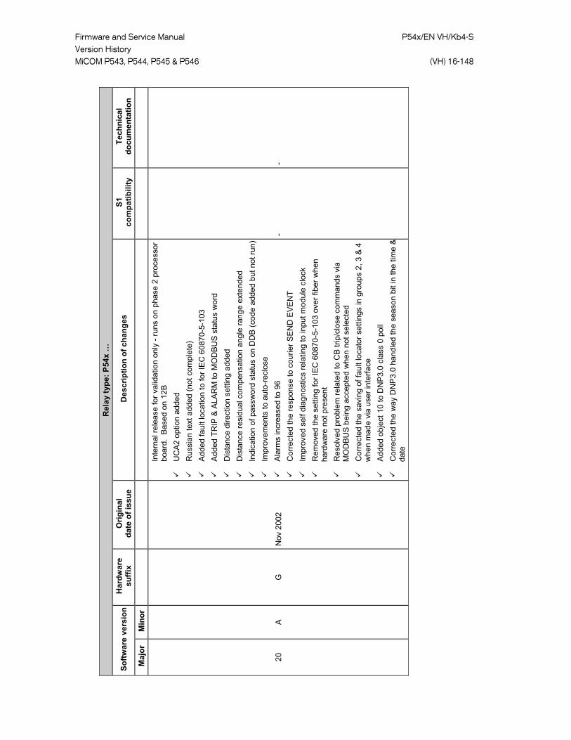
Firmware and Service Manual P54x/EN VH/Kb4-S Version History MiCOM P543, P544, P545 & P546 (VH) 16-148
Rel
ay ty
pe: P
54x
…
Softw
are
vers
ion
Har
dwar
e su
ffix
Orig
inal
da
te o
f iss
ue
Des
crip
tion
of c
hang
es
S1
co
mpa
tibili
ty
Tech
nica
l do
cum
enta
tion
Maj
or
Min
or
20
A
G
Nov
200
2
In
tern
al re
leas
e fo
r val
idat
ion
only
- ru
ns o
n ph
ase
2 pr
oces
sor
bo
ard.
Bas
ed o
n 12
B �
U
CA2
opt
ion
adde
d �
R
ussi
an te
xt a
dded
(not
com
plet
e)
�
Add
ed fa
ult l
ocat
ion
to fo
r IE
C 6
0870
-5-1
03
�
Add
ed T
RIP
& A
LAR
M to
MO
DB
US
sta
tus
wor
d �
D
ista
nce
dire
ctio
n se
tting
add
ed
�
Dis
tanc
e re
sidu
al c
ompe
nsat
ion
angl
e ra
nge
exte
nded
�
In
dica
tion
of p
assw
ord
stat
us o
n D
DB
(cod
e ad
ded
but n
ot ru
n)�
Im
prov
emen
ts to
aut
o-re
clos
e �
A
larm
s in
crea
sed
to 9
6 �
C
orre
cted
the
resp
onse
to c
ourie
r SE
ND
EV
EN
T �
Im
prov
ed s
elf d
iagn
ostic
s re
latin
g to
inpu
t mod
ule
cloc
k �
R
emov
ed th
e se
tting
for I
EC
608
70-5
-103
ove
r fib
er w
hen
hard
war
e no
t pre
sent
�
R
esol
ved
prob
lem
rela
ted
to C
B tr
ip/c
lose
com
man
ds v
ia
MO
DB
US
bei
ng a
ccep
ted
whe
n no
t sel
ecte
d �
C
orre
cted
the
savi
ng o
f fau
lt lo
cato
r set
tings
in g
roup
s 2,
3 &
4
whe
n m
ade
via
user
inte
rface
�
A
dded
obj
ect 1
0 to
DN
P3.
0 cl
ass
0 po
ll �
C
orre
cted
the
way
DN
P3.
0 ha
ndle
d th
e se
ason
bit
in th
e tim
e &
da
te
- -

P54x/EN VH/Kb4-S Firmware and Service Manual Version History (VH) 16-149 MiCOM P543, P544, P545 & P546
Rel
ay ty
pe: P
54x
…
Softw
are
vers
ion
Har
dwar
e su
ffix
Orig
inal
da
te o
f iss
ue
Des
crip
tion
of c
hang
es
S1
co
mpa
tibili
ty
Tech
nica
l do
cum
enta
tion
Maj
or
Min
or
B
G
Apr
200
3
Inte
rnal
rele
ase
for v
alid
atio
n on
ly.
Bas
ed o
n 20
A
�
Enh
ance
d ch
eck
sync
hron
izat
ion
feat
ure
�
Con
trol i
nput
s en
hanc
emen
ts in
clud
ing
non-
vola
tile,
latc
hed,
pu
lsed
and
sup
port
for D
NP3
.0 p
ulse
d �
B
BR
AM
use
d in
dis
turb
ance
reco
rder
opt
imiz
ed
�
Res
olve
d se
vera
l pro
blem
s re
late
d to
the
IEC
608
70-5
-103
pr
otoc
ol
�
Res
olve
d pr
oble
m w
hich
may
cau
se s
hort
dura
tion
curr
ent
diffe
rent
ial t
rips
�
Impr
oved
sel
f dia
gnos
tics
rela
ting
to in
put m
odul
e cl
ock
�
Mod
ified
cou
rier b
lock
tran
sfer
mec
hani
sm s
o it
can
hand
le
mor
e th
an 2
55 b
lock
s
- -
B
G
Apr
200
3
�
PS
L lo
gic
for u
ser d
efin
ed in
tertr
ips
corre
cted
P54
5 &
P54
6 �
P
erm
issi
ve in
tertr
ip in
dua
l red
unda
nt s
chem
es c
orre
cted
�
O
pera
tion
of m
anua
l res
et a
larm
s co
rrect
ed
�
A n
umbe
r of b
ug fi
xes
rela
ting
to C
PU
2
- -
20 C
ont.
C
G
Apr
200
3 In
tern
al re
leas
e fo
r val
idat
ion
only
. B
ased
on
20B
�
C
B c
ontro
l via
hot
key
s �
A
num
ber o
f bug
fixe
s re
latin
g to
CP
U2
- -

Firmware and Service Manual P54x/EN VH/Kb4-S Version History MiCOM P543, P544, P545 & P546 (VH) 16-150
Rel
ay ty
pe: P
54x
…
Softw
are
vers
ion
Har
dwar
e su
ffix
Orig
inal
da
te o
f iss
ue
Des
crip
tion
of c
hang
es
S1
co
mpa
tibili
ty
Tech
nica
l do
cum
enta
tion
Maj
or
Min
or
D
G
Jul 2
003
Inte
rnal
rele
ase
for v
alid
atio
n on
ly.
Bas
ed o
n 20
C
�
Cha
nges
to c
lock
reco
very
circ
uits
to im
prov
e op
erat
ion
with
m
ultip
lexe
rs
�
Pre
vent
ed u
nwan
ted
com
ms.
del
ay a
larm
s �
E
nhan
ced
auto
-recl
ose
feat
ure
adde
d �
A
larm
s ha
ndle
d be
tter i
n C
S10
3 G
I �
Ti
me
sync
hron
izat
ion
via
opto
add
ed
�
Pla
tform
ala
rms
copi
ed to
DD
B
�
Cor
rect
ion
to o
pera
tion
of re
set r
elay
s/LE
Ds
opto
. �
B
acku
p pr
otec
tion
run
if co
-pro
cess
or fa
ils to
sta
rt up
on
pow
er
on
�
Cor
rect
ion
to c
ell 0
B25
�
A
num
ber o
f bug
fixe
s re
latin
g to
CP
U2
V2.
09 o
r Lat
er
P54
x/E
N T
/F32
20 C
ont.
E
G
Oct
200
3
Lim
ited
rele
ase
for N
iCA
P +
sel
ecte
d ot
hers
�
E
xtra
ctio
n of
dis
turb
ance
reco
rder
ove
r MO
DB
US
add
ed
�
Res
olve
nuc
leus
mis
sing
HIS
R p
robl
ems
�
Enh
ance
men
ts to
IDM
T cu
rves
�
D
ispl
ay o
f num
ber o
f goo
d m
essa
ges
via
MO
DB
US
is
corre
cted
�
A
num
ber o
f bug
fixe
s re
latin
g to
CP
U2
V2.
09 o
r Lat
er
P54
x/E
N T
/F32

P54x/EN VH/Kb4-S Firmware and Service Manual Version History (VH) 16-151 MiCOM P543, P544, P545 & P546
Rel
ay ty
pe: P
54x
…
Softw
are
vers
ion
Har
dwar
e su
ffix
Orig
inal
da
te o
f iss
ue
Des
crip
tion
of c
hang
es
S1
co
mpa
tibili
ty
Tech
nica
l do
cum
enta
tion
Maj
or
Min
or
F G
Fe
b 20
04
Rel
ease
to p
rodu
ctio
n �
U
CA
2: In
crea
se m
ax. p
endi
ng re
ques
ts &
max
. con
nect
ed
clie
nts
�
Enh
ance
d D
NP
3.0
�
Pre
vent
ed D
NP
3.0
time
sync
cau
ses
rela
y to
rebo
ot w
hen
IRIG
-B is
act
ive
�
Cor
rect
ed c
ause
of t
rans
mis
sion
whi
ch m
ay b
e re
turn
ed fo
r "F
ault
Loca
tion"
�
P
reve
nts
rela
y re
boot
ing
durin
g E
MC
AN
SI f
ast t
rans
ient
and
IE
C h
igh
frequ
ency
�
A
num
ber o
f bug
fixe
s re
latin
g to
CP
U2
V2.
09 o
r Lat
er
P54
x/E
N T
/F32
20 C
ont.
G
G
Jun
2004
Rel
ease
to p
rodu
ctio
n. B
ased
on
20F
softw
are
�
Pre
vent
ed re
peat
ed d
ownl
oads
of G
SL
files
with
out E
ther
net
card
rest
art r
eboo
ting
Eth
erne
t car
d �
C
orre
ctio
n to
upl
oadi
ng o
f dis
turb
ance
reco
rds
over
UC
A2
�
Cor
rect
ed o
pera
tion
of E
ther
net c
ard
link
LED
for 1
0 B
ase-
FL
�
Clo
sed
UC
A2
asso
ciat
ion
afte
r "di
rty" c
lient
dis
conn
ectio
n �
M
ade
UC
A2
dist
urba
nce
reco
rd d
irect
ory
serv
ice
com
patib
le
with
PA
CiS
�
C
orre
cted
und
er a
nd o
ver v
olta
ge b
lock
ing
of c
heck
syn
c �
Im
prov
ed s
elf-c
heck
ing
of a
nalo
gue
data
acq
uisi
tion
�
Han
dlin
g of
FA
N in
IEC
608
70-5
-103
impr
oved
�
D
iffer
entia
l int
ertri
p in
IEC
608
70-5
-103
repo
rted
with
cor
rect
FA
N
�
Pre
vent
ed C
diff
fail
alar
m o
ccur
s be
fore
sig
nalin
g fa
il al
arm
for
loss
of c
omm
unic
atio
ns
�
Impr
oved
sel
f che
ckin
g of
SR
AM
V2.
09 o
r Lat
er
P54
x/E
N T
/G42

Firmware and Service Manual P54x/EN VH/Kb4-S Version History MiCOM P543, P544, P545 & P546 (VH) 16-152
Rel
ay ty
pe: P
54x
…
Softw
are
vers
ion
Har
dwar
e su
ffix
Orig
inal
da
te o
f iss
ue
Des
crip
tion
of c
hang
es
S1
co
mpa
tibili
ty
Tech
nica
l do
cum
enta
tion
Maj
or
Min
or
H
G
Oct
200
4
Rel
ease
to p
rodu
ctio
n. B
ased
on
20G
sof
twar
e �
S
RA
M s
elf c
heck
ing
adde
d to
co-
proc
esso
r boa
rd
�
Fixe
d an
inco
rrec
t res
pons
e of
the
sum
mer
time
time
bit i
n IE
C 6
0870
-5-1
03 p
roto
col
�
Pre
vent
ed in
corre
ct b
ehav
ior o
f P54
5/P
546
whe
n on
e re
lay
is
ener
gize
d w
hen
ther
e is
noi
se o
n th
e si
gnal
ing
chan
nel
�
Sta
tus
of lo
cal G
PS
repo
rted
inco
rrect
ly in
dua
l red
unda
nt
sche
mes
�
A
ccur
acy
of M
OD
BU
S ti
me
sync
impr
oved
�
Fi
xed
an in
corr
ect r
espo
nse
of th
e su
mm
ertim
e tim
e bi
t in
IE
C 6
0870
-5-1
03 p
roto
col
�
Pre
vent
ed E
ther
net c
ard
rest
artin
g af
ter a
ppro
xim
atel
y 20
ho
urs
whe
n no
con
nect
ion
mad
e �
Im
prov
emen
ts to
tim
e sy
nc fo
r cou
rier,
CS
103
and
DN
P3.
0 �
In
valid
MO
DB
US
regi
ster
4x0
0966
rem
oved
V2.
09 o
r Lat
er
P54
x/E
N T
/G42
I G
N
ov 2
004
Rel
ease
to p
rodu
ctio
n. B
ased
on
20G
sof
twar
e �
D
ispl
ay o
f no.
val
id m
essa
ges
on L
CD
cor
rect
ed
�
Ope
ratio
n of
CB
mai
nten
ance
ala
rm c
orre
cted
�
C
orre
ctio
ns to
allo
w e
xten
ded
cour
ier c
hara
cter
s to
be
used
in
strin
g se
tting
cel
ls fo
r cou
rier a
nd M
OD
BU
S
�
Cor
rect
ed d
efau
lt di
spla
y of
neu
tral c
urre
nt fo
r 5A
CTs
�
P
reve
nted
a re
boot
for
MO
DB
US
ver
sion
s du
ring
even
t ex
tract
ion
whe
n m
essa
ges
whe
re c
lose
toge
ther
�
C
orre
ctio
n to
pre
vent
the
2nd
rear
com
ms.
lock
ing
up
V2.
09 o
r Lat
er
P54
x/E
N T
/G42
20 C
ont.
J G
A
pr 2
006
Rel
ease
to p
rodu
ctio
n. B
ased
on
20G
sof
twar
e �
C
orre
ctio
n to
IEE
E/U
S in
vers
e re
set s
ettin
g �
C
hang
es to
co-
proc
esso
r sta
rt-up
to e
limin
ate
a tim
ing
prob
lem
V2.
09 o
r Lat
er
P54
x/E
N T
/G42

P54x/EN VH/Kb4-S Firmware and Service Manual Version History (VH) 16-153 MiCOM P543, P544, P545 & P546
Rel
ay ty
pe: P
54x
…
Softw
are
vers
ion
Har
dwar
e su
ffix
Orig
inal
da
te o
f iss
ue
Des
crip
tion
of c
hang
es
S1
co
mpa
tibili
ty
Tech
nica
l do
cum
enta
tion
Maj
or
Min
or
K
G
Apr
200
6
Rel
ease
to p
rodu
ctio
n. B
ased
on
20G
sof
twar
e �
Im
prov
emen
ts to
the
dist
ance
pro
tect
ion
�
Add
inte
rfram
e ga
p to
DN
P3.
0 �
C
orre
ctio
ns to
IRIG
-B
�
Vec
tor g
roup
com
pens
atio
ns fo
r YY
2 an
d Y
Y10
cor
rect
ed
�
Cor
rect
ed re
porti
ng o
f dis
tanc
e &
C d
iff s
tars
ove
r CS
103
�
Rep
orts
the
corre
ct C
OT
for r
eset
LE
Ds
com
man
d se
nt v
ia S
1 �
C
orre
cted
a p
robl
em w
hich
occ
urs
whe
n tw
o re
lays
pow
er u
p w
hen
one
is c
onfig
ured
out
V2.
09 o
r Lat
er
P54
x/E
N T
/G42
L G
P54
5 R
elea
se to
Pro
duct
ion.
Bas
ed o
n 20
K s
oftw
are.
�
R
esol
ved
a pr
oble
m w
hich
inte
rrupt
ed th
e U
CA
2 co
mm
unic
atio
ns p
erio
dica
lly
�
Res
olve
d a
prob
lem
rela
ting
to C
T R
atio
’s n
ot b
eing
rest
ored
w
hen
rest
orin
g de
faul
t set
tings
�
R
esol
ved
a pr
oble
m w
ith th
e D
istu
rban
ce R
ecor
der w
hich
sa
tura
tes
for H
igh
curre
nt le
vels
into
5A
CT.
�
R
esol
ved
prob
lem
with
rela
y re
cogn
isin
g no
n ze
ro e
ntry
in 1
4th
posi
tion
of m
odel
num
ber
V2.
09 o
r Lat
er
P54
x/E
N T
/G42
20
Con
t.
M
G
Nov
200
9
Rel
ease
to P
rodu
ctio
n. B
ased
on
20L
softw
are.
�
Im
prov
emen
ts to
the
GP
S c
ode
�
Impr
ovem
ents
in th
e cl
ock
reco
ver c
ircui
ts u
sed
by th
e D
iffer
entia
l Com
ms
�
Cor
rect
ion
to th
e w
ay la
tche
d LE
D/R
elay
s ar
e cl
eare
d �
C
orre
ctio
n to
aut
orec
lose
ope
ratio
n fo
r sw
itch
on to
faul
t co
nditi
on
�
Pre
vent
ed C
B O
pera
ting
Tim
e di
spla
ying
4.2
95M
s �
B
ug F
ixes
V2.
09 o
r Lat
er
P54
x/E
N T
/G42

Firmware and Service Manual P54x/EN VH/Kb4-S Version History MiCOM P543, P544, P545 & P546 (VH) 16-154
Rel
ay ty
pe: P
54x
…
Softw
are
vers
ion
Har
dwar
e su
ffix
Orig
inal
da
te o
f iss
ue
Des
crip
tion
of c
hang
es
S1
co
mpa
tibili
ty
Tech
nica
l do
cum
enta
tion
Maj
or
Min
or
20 C
ont.
N
G
Rel
ease
to P
rodu
ctio
n. B
ased
on
20M
sof
twar
e.
�
Pre
vent
ed th
e D
iffer
entia
l pro
tect
ion
inhi
bitin
g in
thre
e te
rmin
al
sche
mes
whe
n G
PS
is e
nabl
ed a
nd lo
opba
ck m
ode
sele
cted
�
Fa
ult l
ocat
or m
easu
rem
ents
in o
hms
corre
cted
whe
n 5A
CT
used
or d
ispl
ayed
in p
rimar
y.
V2.
09 o
r Lat
er
P54
x/E
N T
/G42
30
A J
Sep
2004
Rel
ease
d to
sel
ecte
d cu
stom
ers
only
. B
ased
on
20G
�
In
terfa
ce to
opt
ical
mul
tiple
xer (
IEE
E s
tand
ard
C37
.94)
�
S
RA
M c
heck
ing
in c
o-pr
oces
sor
�
Dua
l ran
ge o
ptos
�
A
RE
VA
live
ry &
sof
twar
e ch
ange
s �
E
xten
ded
resi
dual
ang
le in
faul
t loc
ator
to m
atch
dis
tanc
e �
R
enam
e G
OO
SE
sig
nals
in li
ne w
ith P
443
�
Add
virt
ual s
igna
ls, c
ontro
l inp
uts
& u
ser a
larm
s to
DR
in li
ne
with
P44
3 �
R
elay
set
tings
sha
ll be
sto
red
in F
LAS
H E
EP
RO
M in
stea
d of
E
EP
RO
M m
emor
y �
E
xten
d ra
nge
of ti
me
dial
to li
ne u
p w
ith P
140
�
Acc
urac
y of
MO
DB
US
tim
e sy
nc im
prov
ed
�
Inva
lid M
OD
BU
S re
gist
er 4
x009
66 re
mov
ed
�
Impr
ovem
ents
to ti
me
sync
for c
ourie
r, C
S10
3 an
d D
NP
3.0
�
Add
ition
of M
OD
BU
S o
nly
time
and
date
form
at s
ettin
g to
co
mm
on c
ourie
r set
tings
for a
cces
s fro
m th
e ot
her i
nter
face
s �
V
ecto
r gro
up c
ompe
nsat
ions
for Y
Y2
and
YY
10 c
orre
cted
�
P
reve
nted
Eth
erne
t car
d re
star
ting
afte
r app
roxi
mat
ely
20
hour
s w
hen
no c
onne
ctio
n m
ade
�
Pre
vent
ed in
corre
ct b
ehav
ior o
f P54
5/P
546
whe
n on
e re
lay
is
ener
gize
d w
hen
ther
e is
noi
se o
n th
e si
gnal
ing
chan
nel
V2.
09 o
r Lat
er (N
o la
ngua
ge fi
le
supp
ort)
P54
x/E
N T
/G42

P54x/EN VH/Kb4-S Firmware and Service Manual Version History (VH) 16-155 MiCOM P543, P544, P545 & P546
Rel
ay ty
pe: P
54x
…
Softw
are
vers
ion
Har
dwar
e su
ffix
Orig
inal
da
te o
f iss
ue
Des
crip
tion
of c
hang
es
S1
co
mpa
tibili
ty
Tech
nica
l do
cum
enta
tion
Maj
or
Min
or
B
J N
ov 2
004
Rel
ease
d to
pro
duct
ion
but h
eld.
Bas
ed o
n 30
A
�
Cou
rier,
MO
DB
US
& D
NP
3.0
com
mun
icat
ions
ove
r Fib
er
adde
d V
2.11
or L
ater
P
54x/
EN
T/H
53
C
J N
ov 2
004
Rel
ease
d to
pro
duct
ion.
Bas
ed o
n 30
B
�
Cor
rect
ion
to p
reve
nt th
e 2n
d re
ar c
omm
s. lo
ckin
g up
�
C
orre
ctio
n to
pre
vent
the
front
pan
el U
I and
com
ms.
lock
up
afte
r con
tinue
d op
erat
ion
�
Cha
nges
to c
o-pr
oces
sor s
tart-
up to
elim
inat
e a
timin
g pr
oble
m
V2.
11 o
r Lat
er
P54
x/E
N T
/H53
D
J D
ec 2
004
Rel
ease
d to
pro
duct
ion.
Bas
ed o
n 30
C
�
Impr
ovem
ents
to o
pera
tion
whe
n su
bjec
ted
to m
ultip
le
com
mun
icat
ion
switc
hes
whe
n op
erat
ing
in n
on-G
PS
mod
e V
2.11
or L
ater
P
54x/
EN
T/H
53
E J
Jan
2005
Rel
ease
d to
pro
duct
ion.
Bas
ed o
n 30
D
�
VTS
enh
ance
d to
rest
ore
3 so
ftwar
e ve
rsio
n 20
per
form
ance
fo
r thr
ee p
ole
tripp
ing
whi
st k
eepi
ng th
e im
prov
emen
ts fo
r 1
pole
trip
ping
add
ed a
t 30B
V2.
11 o
r Lat
er
P54
x/E
N T
/H53
F J
Mar
200
5
Rel
ease
d to
pro
duct
ion.
Bas
ed o
n 30
E
�
Enh
ance
men
ts to
the
curre
nt d
iffer
entia
l per
form
ance
und
er
switc
hed
com
mun
icat
ion
chan
nels
�
C
orre
ctio
n to
the
CS
103
map
ping
for p
latfo
rm a
larm
s
V2.
11 o
r Lat
er
P54
x/E
N T
/H53
G
J A
pr 2
006
Rel
ease
d to
pro
duct
ion.
Bas
ed o
n 30
E
�
Cor
rect
ion
to IE
EE
/US
Inve
rse
rese
t set
ting
V2.
11 o
r Lat
er
P54
x/E
N T
/H53
30 C
ont.
H
J A
pr 2
006
Lim
ited
rele
ase
P54
2 D
NP
3.0
to a
cus
tom
er
�
Add
inte
rfram
e ga
p to
DN
P3.
0 V
2.11
or L
ater
P
54x/
EN
T/H
53

Firmware and Service Manual P54x/EN VH/Kb4-S Version History MiCOM P543, P544, P545 & P546 (VH) 16-156
Rel
ay ty
pe: P
54x
…
Softw
are
vers
ion
Har
dwar
e su
ffix
Orig
inal
da
te o
f iss
ue
Des
crip
tion
of c
hang
es
S1
co
mpa
tibili
ty
Tech
nica
l do
cum
enta
tion
Maj
or
Min
or
30 C
ont.
I J
May
200
5
Rel
ease
d to
pro
duct
ion.
Bas
ed o
n 30
G
�
Impr
ovem
ents
to th
e di
stan
ce p
rote
ctio
n �
A
dd in
terfr
ame
gap
to D
NP
3.0
�
Cor
rect
ions
to IR
IG-B
�
V
ecto
r gro
up c
ompe
nsat
ions
for Y
Y2
and
YY
10 c
orre
cted
�
C
orre
cted
repo
rting
of d
ista
nce
& C
diff
sta
rs o
ver C
S10
3 �
R
epor
ts th
e co
rrect
CO
T fo
r res
et L
ED
s co
mm
and
sent
via
S1
�
Cor
rect
ed a
pro
blem
whi
ch o
ccur
s w
hen
two
rela
ys p
ower
up
whe
n on
e is
con
figur
ed o
ut
�
Mod
ifica
tion
to a
llow
indi
vidu
al M
OD
BU
S re
gist
er a
cces
s
V2.
11 o
r Lat
er
P54
x/E
N T
/H53
40
A
K
May
200
6
Rel
ease
of P
543,
P54
4, P
545
& P
546
with
out d
ista
nce
prot
ectio
n �
C
TS
�
Def
initi
ve ti
me
dire
ctio
nal n
egat
ive
sequ
ence
ove
rcur
rent
I2>
�
GP
S s
ynch
roni
zatio
n of
cur
rent
diff
eren
tial i
n al
l mod
els
�
P54
3 an
d P
545
now
faci
litat
e in
zon
e tra
nsfo
rmer
-feed
er
appl
icat
ions
�
A
ll m
odel
s su
ppor
t AB
C a
nd A
CB
pha
se ro
tatio
n �
S
tand
ard
and
Inve
rted
CT
pola
rity
setti
ng fo
r eac
h se
t of C
Ts
in th
e re
lay
�
Use
r int
erfa
ce w
ith tr
i col
ored
LE
D a
nd fu
nctio
n ke
ys
�
Inte
rMiC
OM
64
�
Volta
ge p
rote
ctio
n �
B
ackw
ards
com
patib
ility
mod
e
Pat
ch fo
r V2.
12
P54
x/E
N M
/I64

P54x/EN VH/Kb4-S Firmware and Service Manual Version History (VH) 16-157 MiCOM P543, P544, P545 & P546
Rel
ay ty
pe: P
54x
…
Softw
are
vers
ion
Har
dwar
e su
ffix
Orig
inal
da
te o
f iss
ue
Des
crip
tion
of c
hang
es
S1
co
mpa
tibili
ty
Tech
nica
l do
cum
enta
tion
Maj
or
Min
or
41
C
K Ju
l 200
6
Rel
ease
of P
543,
P54
4, P
545
& P
546
with
out d
ista
nce
prot
ectio
n ba
sed
on 4
0A
�
IEC
618
50-8
-1
�
Hig
h br
eak
optio
ns
�
Dem
odul
ated
IRIG
-B o
ptio
ns
�
Red
uctio
n of
dis
tanc
e m
inim
um re
ach
setti
ngs
to 0
.05
ohm
�
P
erm
issi
ve tr
ip re
info
rcem
ent
�
Pol
edea
d m
odifi
catio
ns fo
r Hyd
ro Q
uebe
c �
C
S10
3/au
to-r
eclo
se m
odifi
catio
ns
Pat
ch fo
r V2.
12
P54
x/E
N M
/J74
41
D
K Au
g 20
06
Rel
ease
of P
543,
P54
4, P
545
& P
546
with
out d
ista
nce
prot
ectio
n ba
sed
on 4
1C
�
Pre
vent
s a
poss
ible
rebo
ot 1
5 m
inut
es a
fter b
row
sing
the
front
co
urie
r por
t but
not
mak
ing
a se
tting
cha
nge
i.e. b
row
sing
usi
ng
PA
S&
T.
�
Ext
ende
d G
OO
SE
Enr
olm
ent C
apab
ility
�
Cor
rect
ion
to IC
D fi
les,
Enu
mer
atio
n (v
alue
) and
Fix
ed d
ata
Map
ping
Pat
ch fo
r V2.
12
P54
x/E
N M
/J74
41
E K
Nov
200
6
Rel
ease
of P
543,
P54
4, P
545
& P
546
with
out d
ista
nce
prot
ectio
n ba
sed
on 4
1D
�
Pre
vent
a re
boot
in 6
1850
bui
lds
whe
n N
IC li
nk is
inac
tive
and
aval
anch
e of
DD
B a
ctiv
ity.
�
Cor
rect
ly re
port
a fa
tal e
rror g
ener
ated
by
the
sam
plin
g ca
ll-ba
ck
�
Cor
rect
the
oper
atio
n of
the
GO
OSE
mes
sagi
ng a
nd a
pro
blem
w
ith th
e do
wnl
oad
of a
n IE
D C
onfig
urat
ion
file.
�
C
orre
ct th
e op
erat
ion
of th
e ch
eck
sync
. �
C
orre
ct th
e op
erat
ion
of th
e ov
ercu
rren
t res
et c
urve
s.
�
Rem
oved
che
ck o
n th
e14t
h po
sitio
n of
mod
el n
umbe
r �
Fi
xed
Tele
gram
s fo
r pub
lic in
f 64-
67
�
SO
TF c
an o
pera
te e
ven
whe
n it
is d
isab
led
Pat
ch fo
r V2.
12
P54
x/E
N M
/J74

Firmware and Service Manual P54x/EN VH/Kb4-S Version History MiCOM P543, P544, P545 & P546 (VH) 16-158
Rel
ay ty
pe: P
54x
…
Softw
are
vers
ion
Har
dwar
e su
ffix
Orig
inal
da
te o
f iss
ue
Des
crip
tion
of c
hang
es
S1
co
mpa
tibili
ty
Tech
nica
l do
cum
enta
tion
Maj
or
Min
or
41
F K
M
ay 2
007
Rel
ease
of P
543,
P54
4, P
545
& P
546
with
out d
ista
nce
prot
ectio
n ba
sed
on 4
1E
�
Pre
vent
a fa
tal e
rror f
rom
an
inco
rrect
DN
P a
ddre
ss in
not
us
ing
DN
P e
volu
tions
pla
tform
. �
D
efau
lt se
tting
for 4
50B
'I<
Cur
rent
Set
' red
uced
to 5
0mA
�
Fr
ench
Tra
nsla
tions
for D
DB
s 13
68-1
371c
orre
cted
�
Fu
n &
INF
valu
es re
late
d to
CS
103
Com
man
d B
lock
ing
corre
cted
�
A
ngle
for n
egat
ive
sequ
ence
pha
se o
verc
urre
nt s
ettin
g co
rrect
ed
�
Cor
rect
ed o
pera
tion
whe
n us
ing
MiC
OM
S1
is u
sed
to a
ctiv
ate
Set
tings
gro
up b
y rig
ht c
licki
ng o
n th
e gr
oup.
�
C
orre
cted
the
latc
hing
of F
unct
ion
Key
DD
B s
igna
ls o
n re
lay
pow
er u
p �
C
orre
cted
Dis
turb
ance
reco
rder
sca
ling
to p
reve
nt h
igh
curr
ent
leve
ls in
to 5
A C
T ca
usin
g th
e D
istu
rban
ce R
ecor
der t
o sa
tura
te�
R
estri
ng d
efau
lts a
ppea
rs n
ot to
cha
nge
the
1/5A
CT
sele
ctio
n�
C
orre
cted
the
perfo
rman
ce o
f the
IM64
Dire
ct m
ode
�
CB
con
trol v
ia D
irect
acc
ess
does
not
wor
k w
ith 2
CB
ver
sion
s of
P54
0D
�
Aut
orec
lose
dea
d tim
e/cl
ose
cycl
e co
ntin
ues
even
if A
R
switc
hed
out o
f ser
vice
�
C
h2 S
tatis
tics
may
not
be
disp
laye
d
Pat
ch fo
r V2.
12
P54
x/E
N M
/J74
41
G
K
P54
3, P
544,
P54
5 &
P54
6 no
n 61
850
build
s w
ithou
t dis
tanc
e pr
otec
tion
base
d on
41F
was
app
rove
d fo
r rel
ease
but
with
draw
n be
fore
rele
ase.
�
C
orre
ctio
ns to
ena
ble/
disa
ble
of A
utor
eclo
se
Pat
ch fo
r V2.
12
P54
x/E
N M
/J74
41
H
K
May
200
7 R
elea
se o
f P54
3, P
544,
P54
5 &
P54
6 w
ithou
t dis
tanc
e pr
otec
tion
base
d on
41G
�
C
orre
ctio
ns to
ena
ble/
disa
ble
of A
utor
eclo
se
Pat
ch fo
r V2.
12
P54
x/E
N M
/J74

P54x/EN VH/Kb4-S Firmware and Service Manual Version History (VH) 16-159 MiCOM P543, P544, P545 & P546
Rel
ay ty
pe: P
54x
…
Softw
are
vers
ion
Har
dwar
e su
ffix
Orig
inal
da
te o
f iss
ue
Des
crip
tion
of c
hang
es
S1
co
mpa
tibili
ty
Tech
nica
l do
cum
enta
tion
Maj
or
Min
or
42
A
K
Rel
ease
of P
543,
P54
4, P
545
& P
546
with
out d
ista
nce
prot
ectio
n �
C
hine
se in
terfa
ce
�
Rep
laci
ng th
e ex
istin
g D
NP3
with
the
DN
P3
evol
utio
ns
�
Rep
lace
men
t of e
xist
ing
nega
tive
sequ
ence
ove
rcur
rent
with
m
ulti
stag
e (2
IDM
T +
2 D
T) n
egat
ive
sequ
ence
ove
rcur
rent
. �
A
dditi
on o
f ID
G c
urve
, com
mon
ly u
sed
in S
wed
en, t
o E
arth
Fa
ult &
Sen
sitiv
e E
arth
Fau
lt (in
volv
es m
ovin
g se
tting
s)
�
Red
uctio
n of
all
TMS
ste
p si
zes
to 0
.005
�
A
dditi
on o
f Cha
nnel
pro
paga
tion
dela
y S
tatis
tics
and
Ala
rms
�
Cha
nges
to C
TS s
o bo
th te
chni
ques
can
be
sele
cted
toge
ther
�
R
egro
upin
g of
CTS
set
tings
�
A
dditi
on o
f fou
r sta
ges
of u
nder
freq
uenc
y pr
otec
tion
and
two
stag
es o
f Ove
rfreq
uenc
y pr
otec
tion
�
Add
ition
of d
f/dt p
rote
ctio
n �
C
hang
es to
Und
er a
nd O
verv
olta
ge to
ena
ble
each
sta
ge to
be
inde
pend
ently
set
�
E
xten
sion
s to
the
chec
ksyn
c V
T po
sitio
n se
tting
�
C
hang
es to
Per
mis
sive
Inte
r Trip
(PIT
) log
ic to
ena
ble
the
user
to
sel
ect e
ither
loca
l or r
emot
e cu
rrent
to b
e us
ed.
�
Incl
udes
loca
l tim
e zo
ne s
ettin
gs fo
r Dat
e &
Tim
e �
R
educ
ed m
inim
um s
ettin
g fo
r IN
> I2
pol S
et
�
Add
ition
of p
ropa
gatio
n de
lay
times
to F
ault
Rec
ord
�
Def
ault
setti
ng fo
r 450
B 'I
< C
urre
nt S
et' r
educ
ed to
50m
A.
�
Enh
ance
men
t to
self
chec
king
of o
utpu
t rel
ays
�
Cha
nge
tunn
elle
d co
urie
r add
ress
to fo
llow
the
1st R
ear P
ort’s
K
BU
S o
r CS
103
addr
ess.
Pat
ch fo
r V2.
12
P54
x_E
N_M
J74
+ ad
dend
um
P54x
_EN
_AD
_J84

Firmware and Service Manual P54x/EN VH/Kb4-S Version History MiCOM P543, P544, P545 & P546 (VH) 16-160
Rel
ay ty
pe: P
54x
…
Softw
are
vers
ion
Har
dwar
e su
ffix
Orig
inal
da
te o
f iss
ue
Des
crip
tion
of c
hang
es
S1
co
mpa
tibili
ty
Tech
nica
l do
cum
enta
tion
Maj
or
Min
or
42
B K
July
200
7
Rel
ease
of P
543,
P54
4, P
545
& P
546
with
out d
ista
nce
prot
ectio
n ba
sed
on 4
2A.
�
Impr
ovem
ents
to V
TS
�
Cor
rect
ions
to e
nabl
e/di
sabl
e of
Aut
orec
lose
�
R
esol
ved
a pr
oble
m re
latin
g to
CT
Rat
io’s
not
bei
ng re
stor
ed
whe
n re
stor
ing
defa
ult s
ettin
gs
�
Res
olve
d a
prob
lem
with
the
Dis
turb
ance
Rec
orde
r whi
ch
satu
rate
s fo
r Hig
h cu
rrent
leve
ls in
to 5
A C
T.
Pat
ch fo
r V2.
12
P54
x_E
N_M
J74
+ ad
dend
um
P54x
_EN
_AD
_J84
42
D
K D
ec 2
007
Rel
ease
of P
543,
P54
4, P
545
& P
546
with
out d
ista
nce
prot
ectio
n ba
sed
on 4
2B.
�
Fixe
d a
num
ber o
f 618
50/G
oose
pro
blem
s �
M
inor
cor
rect
ion
to fa
ult r
ecor
d �
C
orre
ctio
ns to
ove
r vol
tage
sta
ge 2
inhi
bit
�
Fixe
d th
e m
ax p
rop
alar
m
�
Cor
rect
ed s
ome
DD
B G
erm
an te
xt
Pat
ch fo
r V2.
12
P54
x_E
N_M
J74
+ ad
dend
um
P54x
_EN
_AD
_J84
42
E
K
May
200
8
Rel
ease
of P
543,
P54
4, P
545
& P
546
with
out d
ista
nce
prot
ectio
n ba
sed
on 4
2D.
�
Fixe
d a
num
ber o
f 618
50 p
robl
ems
�
Impr
oved
co-
proc
esso
r err
or re
porti
ng
�
Fixe
d In
hibi
t CB
Fai
l Pro
tect
ion
in P
544/
6
Pat
ch fo
r V2.
12
P54
x_E
N_M
J74
+ ad
dend
um
P54x
_EN
_AD
_J84
42
F K
Not
rele
ased
to p
rodu
ctio
n. B
ased
on
42E
. �
C
orre
ctio
n to
aut
orec
lose
ope
ratio
n fo
r sw
itch
on to
faul
t co
nditi
on
�
Pre
vent
ed C
B O
pera
ting
Tim
e di
spla
ying
4.2
95M
s �
B
ug fi
xes
Pat
ch fo
r V2.
12
P54
x_E
N_M
J74
+ ad
dend
um
P54x
_EN
_AD
_J84
42
G
K
Oct
200
8
Rel
ease
of P
543,
P54
4, P
545
& P
546
with
out d
ista
nce
prot
ectio
n ba
sed
on 4
2F.
�
Cor
rect
ion
to th
e di
stan
ce c
ross
pol
aris
ing
whe
n th
e m
emor
y ex
pire
s
Pat
ch fo
r V2.
12
P54
x_E
N_M
J74
+ ad
dend
um
P54x
_EN
_AD
_J84

P54x/EN VH/Kb4-S Firmware and Service Manual Version History (VH) 16-161 MiCOM P543, P544, P545 & P546
Rel
ay ty
pe: P
54x
…
Softw
are
vers
ion
Har
dwar
e su
ffix
Orig
inal
da
te o
f iss
ue
Des
crip
tion
of c
hang
es
S1
co
mpa
tibili
ty
Tech
nica
l do
cum
enta
tion
Maj
or
Min
or
42
H
K
Sep
t 200
9
Rel
ease
of P
543,
P54
4, P
545
& P
546
with
out d
ista
nce
prot
ectio
n ba
sed
on 4
2G.
�
Cor
rect
ed s
ome
men
u tra
nsla
tions
�
C
orre
cted
Bre
aker
Fai
l - W
I Aid
ed1
trips
so
they
can
be
disa
bled
via
set
ting
"WI P
rot R
eset
" �
Ti
mes
tam
p in
faul
t rec
ord
adju
sted
for t
he lo
cal t
ime
setti
ng.
�
Cor
rect
ed P
543
defa
ult P
SL
�
Cor
rect
ions
to th
e C
urre
nt D
iffer
entia
l Inh
ibit
whe
n th
e G
PS
sy
nchr
onis
atio
n is
dis
able
d �
C
orre
cted
The
rmal
Sta
te m
easu
rem
ent v
ia D
NP
3 �
C
orre
ctio
n to
the
way
latc
hed
LED
/Rel
ays
are
clea
red
�
Cor
rect
ion
to N
egat
ive
sequ
ence
ove
rcur
rent
set
tings
whe
n 5A
in
put u
sed
�
Cor
rect
ion
to P
545/
P541
com
patib
ility
whe
n us
ed in
tra
nsfo
rmer
com
pens
atio
n m
ode
�
Impr
ovem
ents
to th
e G
PS
cod
e �
P
reve
nted
CTS
gen
erat
ing
even
ts w
hen
CTS
is d
isab
led
�
Pre
vent
Z5
from
set
ting
slow
sw
ing
whe
n P
SB
is d
isab
led
�
Fixe
d pr
oble
m w
hich
pre
vent
ed re
sidu
al o
verv
olta
ge fr
om
initi
atin
g C
B F
ail
�
Var
ious
impr
ovem
ents
to D
NP
, CS
103
& IE
C61
850
prot
ocol
s �
B
ug fi
xes
Pat
ch fo
r V2.
12
P54
x_E
N_M
J74
+ ad
dend
um
P54x
_EN
_AD
_J84

Firmware and Service Manual P54x/EN VH/Kb4-S Version History MiCOM P543, P544, P545 & P546 (VH) 16-162
Rel
ay ty
pe: P
54x
…
Softw
are
vers
ion
Har
dwar
e su
ffix
Orig
inal
da
te o
f iss
ue
Des
crip
tion
of c
hang
es
S1
co
mpa
tibili
ty
Tech
nica
l do
cum
enta
tion
Maj
or
Min
or
44
A
K
Mar
200
8
Rel
ease
of P
543,
P54
4, P
545
& P
546
with
out d
ista
nce
prot
ectio
n ba
sed
on 4
2D.
�
Pos
ition
al in
form
atio
n ad
ded
to P
SL.
�
D
NP
3.0
Ove
r Eth
erne
t pro
toco
l add
ed.
�
Ext
ende
d I/O
– s
tatu
s in
puts
incr
ease
d fro
m 2
4 to
32.
�
C
ompe
nsat
ed o
verv
olta
ge p
rote
ctio
n ad
ded
�
IEC
-103
Gen
eric
Ser
vice
s M
easu
rem
ents
add
ed
�
Set
/Res
et L
atch
Log
ic G
ates
add
ed to
PS
L �
Fa
ult r
ecor
d to
incl
ude
curr
ent d
iffer
entia
l cur
rent
s re
cord
ed a
t th
e tim
e of
the
curre
nt d
iffer
entia
l trip
in a
dditi
on to
the
exis
ting
data
from
1 c
ycle
late
r. �
Fa
ult r
ecor
d in
crea
sed
max
num
ber o
f fau
lt re
cord
s to
15
�
GP
S A
larm
mod
ifica
tions
�
D
NP
enh
ance
men
ts fo
r SS
E
�
Bug
fixe
s
Pat
ch fo
r V2.
14
Firs
t rel
ease
of
Stud
io
P54
x_E
N_M
J74
+ ad
dend
um
P54x
_EN
_AD
_J94
44
B K
Jun
2008
Rel
ease
of P
543,
P54
4, P
545
& P
546
with
out d
ista
nce
prot
ectio
n ba
sed
on 4
4A.
�
Fixe
d a
num
ber o
f 618
50 p
robl
ems
�
Impr
oved
co-
proc
esso
r err
or re
porti
ng
�
Fixe
d In
hibi
t CB
Fai
l Pro
tect
ion
in P
544/
6 �
C
orre
cted
som
e Fr
ench
and
Ger
man
text
�
P
reve
nted
CB
Ope
ratin
g Ti
me
disp
layi
ng 4
.295
Ms
�
Fixe
d a
prob
lem
whi
ch p
reve
nted
ext
ract
ion
of d
np3
setti
ng
files
from
dnp
3 ov
er E
ther
net v
aria
nts.
Pat
ch fo
r V2.
14
Firs
t rel
ease
of
Stud
io
P54
x_E
N_M
J74
+ ad
dend
um
P54x
_EN
_AD
_J94

P54x/EN VH/Kb4-S Firmware and Service Manual Version History (VH) 16-163 MiCOM P543, P544, P545 & P546
Rel
ay ty
pe: P
54x
…
Softw
are
vers
ion
Har
dwar
e su
ffix
Orig
inal
da
te o
f iss
ue
Des
crip
tion
of c
hang
es
S1
co
mpa
tibili
ty
Tech
nica
l do
cum
enta
tion
Maj
or
Min
or
44
D
K Ja
n 20
09
Rel
ease
of P
543,
P54
4, P
545
& P
546
with
out d
ista
nce
prot
ectio
n ba
sed
on 4
4B.
�
Cor
rect
ions
to th
e C
urre
nt D
iffer
entia
l Inh
ibit
whe
n th
e G
PS
sy
nchr
oniz
atio
n is
dis
able
d �
C
orre
cted
The
rmal
Sta
te m
easu
rem
ent v
ia D
NP
3 �
Ti
mes
tam
p in
faul
t rec
ord
adju
sted
for t
he lo
cal t
ime
setti
ng.
�
Cor
rect
ed B
reak
er F
ail -
WI A
ided
1 tri
ps s
o th
ey c
an b
e di
sabl
ed v
ia s
ettin
g "W
I Pro
t Res
et"
Pat
ch fo
r V2.
14
Firs
t rel
ease
of
Stud
io
P54
x_E
N_M
J74
+ ad
dend
um
P54x
_EN
_AD
_J94
44
E
K
Mar
200
9
Rel
ease
of P
543,
P54
4, P
545
& P
546
with
out d
ista
nce
prot
ectio
n ba
sed
on 4
4D.
�
Pre
vent
s th
e lo
ss o
f IE
C61
850
mes
sage
s an
d fix
ed th
e ha
ndlin
g of
the
AC
D fl
ag d
urin
g G
I. �
Im
prov
ed th
e E
ther
net c
ard
boot
cod
e
Pat
ch fo
r V2.
14
Firs
t rel
ease
of
Stud
io
P54
x_E
N_M
J74
+ ad
dend
um
P54x
_EN
_AD
_J94
44
F K
S
ept 2
009
Rel
ease
of P
543,
P54
4, P
545
& P
546
with
out d
ista
nce
prot
ectio
n ba
sed
on 4
4E.
�
Cor
rect
ed s
ome
men
u tra
nsla
tions
�
C
orre
cted
P54
3 de
faul
t PS
L �
C
orre
ctio
n to
the
way
latc
hed
LED
/Rel
ays
are
clea
red
�
Cor
rect
ion
to N
egat
ive
sequ
ence
ove
rcur
rent
set
tings
whe
n 5A
in
put u
sed
�
Cor
rect
ion
to P
545/
P541
com
patib
ility
whe
n us
ed in
tra
nsfo
rmer
com
pens
atio
n m
ode
�
Impr
ovem
ents
to th
e G
PS
cod
e �
P
reve
nted
CTS
gen
erat
ing
even
ts w
hen
CTS
is d
isab
led
�
Fixe
d pr
oble
m w
hich
pre
vent
ed re
sidu
al o
verv
olta
ge fr
om
initi
atin
g C
B F
ail
�
Var
ious
impr
ovem
ents
to D
NP
, CS
103
& IE
C61
850
prot
ocol
s �
B
ug fi
xes
Pat
ch fo
r V2.
14
Firs
t rel
ease
of
Stud
io
P54
x_E
N_M
J74
+ ad
dend
um
P54x
_EN
_AD
_J94

Firmware and Service Manual P54x/EN VH/Kb4-S Version History MiCOM P543, P544, P545 & P546 (VH) 16-164
Rel
ay ty
pe: P
54x
…
Softw
are
vers
ion
Har
dwar
e su
ffix
Orig
inal
da
te o
f iss
ue
Des
crip
tion
of c
hang
es
S1
co
mpa
tibili
ty
Tech
nica
l do
cum
enta
tion
Maj
or
Min
or
45
B
K
Mar
200
9
Rel
ease
of P
543,
P54
4, P
545
& P
546
with
out d
ista
nce
prot
ectio
n ba
sed
on 4
4E.
�
Aut
orec
lose
, Che
ck S
ync
and
CB
Mon
itorin
g ad
ded
to P
544
&
P546
Pat
ch fo
r V2.
14
Stu
dio
ftp s
erve
r P
54x/
EN
M/K
A4
45
C
K
May
200
9
Rel
ease
of P
543,
P54
4, P
545
& P
546
with
out d
ista
nce
prot
ectio
n ba
sed
on 4
5B.
�
Impr
ovem
ents
to th
e E
ther
net c
ard
star
tup
and
conf
igur
atio
n �
C
orre
ctio
n to
Neg
ativ
e se
quen
ce o
verc
urre
nt s
ettin
gs w
hen
5A
inpu
t use
d �
C
orre
ctio
n to
P54
5/P5
41 c
ompa
tibilit
y w
hen
used
in
trans
form
er c
ompe
nsat
ion
mod
e �
C
orre
ctio
n to
the
way
latc
hed
LED
/Rel
ays
are
clea
red
�
Cor
rect
ions
to m
enu
text
�
Im
prov
emen
ts to
the
GP
S c
ode
�
Bug
Fix
es
Pat
ch fo
r V2.
14
Stu
dio
ftp s
erve
r P
54x/
EN
M/K
A4
45
D
K
Oct
200
9
Rel
ease
of P
543,
P54
4, P
545
& P
546
with
out d
ista
nce
prot
ectio
n ba
sed
on 4
5C.
�
Impr
ovem
ents
to th
e G
PS
cod
e �
Im
prov
emen
ts to
the
GP
S c
ode
�
Impr
ovem
ents
in th
e cl
ock
reco
ver c
ircui
ts u
sed
by th
e D
iffer
entia
l Com
ms
�
Bug
Fix
es
Pat
ch fo
r V2.
14
Stu
dio
ftp s
erve
r P
54x/
EN
M/K
A4

P54x/EN VH/Kb4-S Firmware and Service Manual Version History (VH) 16-165 MiCOM P543, P544, P545 & P546
Rel
ay ty
pe: P
54x
…
Softw
are
vers
ion
Har
dwar
e su
ffix
Orig
inal
da
te o
f iss
ue
Des
crip
tion
of c
hang
es
S1
co
mpa
tibili
ty
Tech
nica
l do
cum
enta
tion
Maj
or
Min
or
47
A
K
Rel
ease
of P
543,
P54
4, P
545
& P
546
with
out d
ista
nce
prot
ectio
n ba
sed
on 4
5D.
�
IEC
-618
50 p
hase
2 a
nd 2
.1 im
plem
ente
d �
A
pplic
atio
n fo
r Inz
one
Tran
sfor
mer
s (2
nd a
nd 5
th H
arm
onic
B
lock
ing/
rest
rain
t) �
D
iffer
entia
l Hig
hset
can
be
disa
bled
whe
n In
rush
pro
tect
ion
is
enab
led
�
Res
trict
ed E
arth
Fau
lt P
rote
ctio
n (R
EF)
�
M
odifi
catio
n to
Cha
r Mod
tim
er fu
nctio
nalit
y �
S
epar
ate
mea
sure
men
ts fo
r eac
h se
t of C
T’s
�
Inte
rrupt
Driv
en In
terM
iCO
M in
all
mod
els
�
Rea
d O
nly
Mod
e
Pat
ch fo
r V2.
14
Stu
dio
ftp s
erve
r
P54
x/E
N M
/KA
4 +
adde
ndum
P
54x/
EN
AD
/KB
4
47
B K
Jan
2010
Rel
ease
of P
543,
P54
4, P
545
& P
546
with
out d
ista
nce
prot
ectio
n ba
sed
on 4
7A.
�
Pre
vent
ed th
e D
iffer
entia
l pro
tect
ion
inhi
bitin
g in
thre
e te
rmin
al
sche
mes
whe
n G
PS
is e
nabl
ed a
nd lo
opba
ck m
ode
sele
cted
�
Fa
ult l
ocat
or m
easu
rem
ents
in o
hms
corre
cted
whe
n 5A
CT
used
or d
ispl
ayed
in p
rimar
y.
�
Freq
uenc
y m
easu
rem
ent i
n D
NP
3 fa
ult r
ecor
d co
rrect
ed
Pat
ch fo
r V2.
14
Stu
dio
ftp s
erve
r
P54
x/E
N M
/KA
4 +
adde
ndum
P
54x/
EN
AD
/KB
4
50
A
K
May
200
6
Rel
ease
of P
543,
P54
4, P
545
& P
546
with
dis
tanc
e pr
otec
tion
�
Dis
tanc
e pr
otec
tion
from
P44
3 �
D
EF
from
P44
3 �
A
ided
dis
tanc
e &
DE
F sc
hem
es fr
om P
443
�
CTS
Pat
ch fo
r V2.
12
P54
x/E
N M
/I64

Firmware and Service Manual P54x/EN VH/Kb4-S Version History MiCOM P543, P544, P545 & P546 (VH) 16-166
Rel
ay ty
pe: P
54x
…
Softw
are
vers
ion
Har
dwar
e su
ffix
Orig
inal
da
te o
f iss
ue
Des
crip
tion
of c
hang
es
S1
co
mpa
tibili
ty
Tech
nica
l do
cum
enta
tion
Maj
or
Min
or
50 C
ont.
A
K
May
200
6
�
Def
initi
ve ti
me
dire
ctio
nal n
egat
ive
sequ
ence
ove
rcur
rent
I2>
�
GP
S s
ynch
roni
zatio
n of
cur
rent
diff
eren
tial i
n al
l mod
els
�
P54
3 an
d P
545
now
faci
litat
e in
zon
e tra
nsfo
rmer
-feed
er
appl
icat
ions
�
A
ll m
odel
s su
ppor
t AB
C a
nd A
CB
pha
se ro
tatio
n �
S
tand
ard
and
inve
rted
CT
pola
rity
setti
ng fo
r eac
h se
t of C
Ts in
th
e re
lay
�
Use
r int
erfa
ce w
ith tr
i col
ored
LE
D a
nd fu
nctio
n ke
ys
�
Inte
rMiC
OM
64
�
Volta
ge p
rote
ctio
n �
B
ackw
ards
com
patib
ility
mod
e
Pat
ch fo
r V2.
12
P54
x/E
N M
/I64
C
K Ju
l 200
6
Rel
ease
of P
543,
P54
4, P
545
& P
546
with
dis
tanc
e pr
otec
tion
base
d on
50A
�
IE
C 6
1850
-8-1
�
H
igh
brea
k op
tions
�
D
emod
ulat
ed IR
IG-B
opt
ions
�
R
educ
tion
of d
ista
nce
min
imum
reac
h se
tting
s to
0.0
5 oh
m
�
Per
mis
sive
trip
rein
forc
emen
t �
P
oled
ead
mod
ifica
tions
for H
ydro
Que
bec
�
CS
103/
auto
-rec
lose
mod
ifica
tions
�
O
ut o
f ste
p tri
ppin
g
Pat
ch fo
r V2.
12
P54
x/E
N M
/J74
51
D
K Au
g 20
06
Rel
ease
of P
543,
P54
4, P
545
& P
546
with
dis
tanc
e pr
otec
tion
base
d on
51C
�
P
reve
nts
a po
ssib
le re
boot
15
min
utes
afte
r bro
wsi
ng th
e fro
nt
cour
ier p
ort b
ut n
ot m
akin
g a
setti
ng c
hang
e i.e
. bro
wsi
ng u
sing
P
AS
&T.
�
E
xten
ded
GO
OS
E E
nrol
men
t Cap
abilit
y �
C
orre
ctio
n to
ICD
file
s, E
num
erat
ion
(val
ue) a
nd F
ixed
dat
a M
appi
ng
Pat
ch fo
r V2.
12
V2.
13 o
r Lat
er
P54
x_E
N_M
J74

P54x/EN VH/Kb4-S Firmware and Service Manual Version History (VH) 16-167 MiCOM P543, P544, P545 & P546
Rel
ay ty
pe: P
54x
…
Softw
are
vers
ion
Har
dwar
e su
ffix
Orig
inal
da
te o
f iss
ue
Des
crip
tion
of c
hang
es
S1
co
mpa
tibili
ty
Tech
nica
l do
cum
enta
tion
Maj
or
Min
or
51 C
ont.
E
K
Nov
200
6
Rel
ease
of P
543,
P54
4, P
545
& P
546
with
dis
tanc
e pr
otec
tion
base
d on
51D
�
P
reve
nt a
rebo
ot in
618
50 b
uild
s w
hen
NIC
link
is in
activ
e an
d av
alan
che
of D
DB
act
ivity
. �
C
orre
ctly
repo
rt a
fata
l erro
r gen
erat
ed b
y th
e sa
mpl
ing
call-
back
�
C
orre
ct th
e op
erat
ion
of th
e G
OO
SE m
essa
ging
and
a p
robl
em
with
the
dow
nloa
d of
an
IED
Con
figur
atio
n fil
e.
�
Cor
rect
the
oper
atio
n of
the
chec
k sy
nc.
�
Cor
rect
the
oper
atio
n of
the
over
curr
ent r
eset
cur
ves.
�
R
emov
ed c
heck
on
the1
4th
posi
tion
of m
odel
num
ber
�
Fixe
d Te
legr
ams
for p
ublic
inf 6
4-67
�
S
OTF
can
ope
rate
eve
n w
hen
it is
dis
able
d
Pat
ch fo
r V2.
12
V2.
13 o
r Lat
er
P54
x_E
N_M
J74

Firmware and Service Manual P54x/EN VH/Kb4-S Version History MiCOM P543, P544, P545 & P546 (VH) 16-168
Rel
ay ty
pe: P
54x
…
Softw
are
vers
ion
Har
dwar
e su
ffix
Orig
inal
da
te o
f iss
ue
Des
crip
tion
of c
hang
es
S1
co
mpa
tibili
ty
Tech
nica
l do
cum
enta
tion
Maj
or
Min
or
51
F K
M
ay 2
007
Rel
ease
of P
543,
P54
4, P
545
& P
546
non
6185
0 bu
ilds
with
di
stan
ce p
rote
ctio
n ba
sed
on 5
1E
�
Pre
vent
a fa
tal e
rror f
rom
an
inco
rrect
DN
P a
ddre
ss in
not
us
ing
DN
P e
volu
tions
pla
tform
. �
D
efau
lt se
tting
for 4
50B
'I<
Cur
rent
Set
' red
uced
to 5
0 m
A
�
Fren
ch T
rans
latio
ns fo
r DD
Bs
1368
-137
1cor
rect
ed
�
Dep
ende
ncie
s fo
r cel
ls 3
242
& 3
245
corr
ecte
d �
Fu
n &
INF
valu
es re
late
d to
CS
103
Com
man
d B
lock
ing
corre
cted
�
A
ngle
for n
egat
ive
sequ
ence
pha
se o
verc
urre
nt s
ettin
g co
rrect
ed
�
Cor
rect
ed o
pera
tion
whe
n us
ing
MiC
OM
S1
is u
sed
to a
ctiv
ate
Set
tings
gro
up b
y rig
ht c
licki
ng o
n th
e gr
oup.
�
C
orre
cted
the
latc
hing
of F
unct
ion
Key
DD
B s
igna
ls o
n re
lay
pow
er u
p �
C
orre
cted
Dis
turb
ance
reco
rder
sca
ling
to p
reve
nt h
igh
curr
ent
leve
ls in
to 5
A C
T ca
usin
g th
e D
istu
rban
ce R
ecor
der t
o sa
tura
te�
R
estri
ng d
efau
lts a
ppea
rs n
ot to
cha
nge
the
1/5A
CT
sele
ctio
n�
C
orre
cted
the
perfo
rman
ce o
f the
IM64
Dire
ct m
ode
�
CB
con
trol v
ia D
irect
acc
ess
does
not
wor
k w
ith 2
CB
ver
sion
s of
P54
0D
�
Aut
orec
lose
dea
d tim
e/cl
ose
cycl
e co
ntin
ues
even
if A
R
switc
hed
out o
f ser
vice
�
D
ista
nce
setti
ng a
re n
ot u
pdat
ed in
sim
ple
setti
ng m
ode
in
setti
ng g
roup
s ot
her t
han
the
activ
e on
e �
C
h2 S
tatis
tics
may
not
be
disp
laye
d
Pat
ch fo
r V2.
12
V2.
13 o
r Lat
er
P54
x_E
N_M
J74
51
G
K
P
543,
P54
4, P
545
& P
546
non
6185
0 bu
ilds
with
dis
tanc
e
prot
ectio
n ba
sed
on 5
1F w
as a
ppro
ved
for r
elea
se b
ut
w
ithdr
awn
befo
re re
leas
e.
�
Cor
rect
ions
to e
nabl
e/di
sabl
e of
Aut
orec
lose
Pat
ch fo
r V2.
12
P54
x_E
N_M
J74

P54x/EN VH/Kb4-S Firmware and Service Manual Version History (VH) 16-169 MiCOM P543, P544, P545 & P546
Rel
ay ty
pe: P
54x
…
Softw
are
vers
ion
Har
dwar
e su
ffix
Orig
inal
da
te o
f iss
ue
Des
crip
tion
of c
hang
es
S1
co
mpa
tibili
ty
Tech
nica
l do
cum
enta
tion
Maj
or
Min
or
51
H
K Ju
ly 2
007
R
elea
se o
f P54
3, P
544,
P54
5 &
P54
6 no
n 61
850
build
s w
ith
di
stan
ce p
rote
ctio
n ba
sed
on 5
1G.
�
Cor
rect
ed p
ower
sw
ing
dete
ctio
n w
hen
both
dis
tanc
e an
d cu
rrent
diff
eren
tial e
nabl
ed
�
Cor
rect
ions
to e
nabl
e/di
sabl
e of
Aut
orec
lose
Pat
ch fo
r V2.
12
P54
x_E
N_M
J74

Firmware and Service Manual P54x/EN VH/Kb4-S Version History MiCOM P543, P544, P545 & P546 (VH) 16-170
Rel
ay ty
pe: P
54x
…
Softw
are
vers
ion
Har
dwar
e su
ffix
Orig
inal
da
te o
f iss
ue
Des
crip
tion
of c
hang
es
S1
co
mpa
tibili
ty
Tech
nica
l do
cum
enta
tion
Maj
or
Min
or
52
A
K
R
elea
se o
f P54
3, P
544,
P54
5 &
P54
6 w
ith d
ista
nce
prot
ectio
n �
C
hine
se in
terfa
ce
�
Rep
laci
ng th
e ex
istin
g D
NP3
with
the
DN
P3
evol
utio
ns
�
Add
ition
of a
cur
rent
but
no
volts
trip
opt
ion
to S
witc
h on
to
Faul
t and
Trip
on
Rec
lose
feat
ure
(SO
TF/T
OR
) �
R
epla
cem
ent o
f exi
stin
g ne
gativ
e se
quen
ce o
verc
urre
nt w
ith
mul
ti st
age
(2 ID
MT
+ 2
DT)
neg
ativ
e se
quen
ce o
verc
urre
nt.
�
Add
ition
of I
DG
cur
ve, c
omm
only
use
d in
Sw
eden
, to
Ear
th
Faul
t & S
ensi
tive
Ear
th F
ault
(invo
lves
mov
ing
setti
ngs)
�
R
educ
tion
of a
ll TM
S s
tep
size
s to
0.0
05
�
Add
ition
of C
hann
el p
ropa
gatio
n de
lay
Sta
tistic
s an
d A
larm
s �
C
hang
es to
CTS
so
both
tech
niqu
es c
an b
e se
lect
ed to
geth
er
�
Reg
roup
ing
of C
TS s
ettin
gs
�
Add
ition
of f
our s
tage
s of
und
er fr
eque
ncy
prot
ectio
n an
d tw
o st
ages
of O
verfr
eque
ncy
prot
ectio
n �
A
dditi
on o
f df/d
t pro
tect
ion
�
Cha
nges
to U
nder
and
Ove
rvol
tage
to e
nabl
e ea
ch s
tage
to b
e in
depe
nden
tly s
et
�
Ext
ensi
ons
to th
e ch
ecks
ync
VT
posi
tion
setti
ng
�
Rep
laci
ng fi
xed
Trip
on
Clo
se (T
OC
) Del
ay w
ith a
set
ting
�
Impr
ovem
ents
to s
low
pow
er s
win
g de
tect
ion
�
Cha
nges
to d
ista
nce
coun
t stra
tegy
to re
stor
e th
e sa
me
oper
atin
g tim
e w
hen
phas
e di
ffere
ntia
l pro
tect
ion
is e
nabl
ed
�
Cha
nges
to P
erm
issi
ve In
ter T
rip (P
IT) l
ogic
to e
nabl
e th
e us
er
to s
elec
t eith
er lo
cal o
r rem
ote
curre
nt to
be
used
. �
In
clud
es lo
cal t
ime
zone
set
tings
for D
ate
& T
ime
Pat
ch fo
r V2.
14
P54
x_E
N_M
J74
+ ad
dend
um
P54x
_EN
_AD
_J84

P54x/EN VH/Kb4-S Firmware and Service Manual Version History (VH) 16-171 MiCOM P543, P544, P545 & P546
Rel
ay ty
pe: P
54x
…
Softw
are
vers
ion
Har
dwar
e su
ffix
Orig
inal
da
te o
f iss
ue
Des
crip
tion
of c
hang
es
S1
co
mpa
tibili
ty
Tech
nica
l do
cum
enta
tion
Maj
or
Min
or
52
A
K
�
Add
ition
of f
lexi
ble
setti
ngs
for d
ista
nce
quad
rilat
eral
top
line
�
Red
uced
min
imum
set
ting
for I
N>
I2po
l Set
�
A
dditi
on o
f pro
paga
tion
dela
y tim
es to
Fau
lt R
ecor
d �
D
efau
lt se
tting
for 4
50B
'I<
Cur
rent
Set
' red
uced
to 5
0mA
. �
E
nhan
cem
ent t
o se
lf ch
ecki
ng o
f out
put r
elay
s �
C
hang
e tu
nnel
led
cour
ier a
ddre
ss to
follo
w th
e 1s
t Rea
r Por
t’s
KB
US
or C
S10
3 ad
dres
s.
52
B K
July
200
7
R
elea
se o
f P54
3, P
544,
P54
5 &
P54
6 w
ith d
ista
nce
prot
ectio
n
base
d on
52A
. �
Ph
ase
com
paris
on p
rote
ctio
n P5
47 a
dded
to ra
nge
�
Impr
ovem
ents
to V
TS
�
Impr
ovem
ents
to s
low
pow
er s
win
g de
tect
ion
�
Cor
rect
ed p
ower
sw
ing
dete
ctin
g w
hen
both
dis
tanc
e an
d cu
rrent
diff
eren
tial e
nabl
ed
�
Cor
rect
ions
to e
nabl
e/di
sabl
e of
Aut
orec
lose
�
R
esol
ved
a pr
oble
m re
latin
g to
CT
Rat
io’s
not
bei
ng re
stor
ed
whe
n re
stor
ing
defa
ult s
ettin
gs
�
Res
olve
d a
prob
lem
with
the
Dis
turb
ance
Rec
orde
r whi
ch
satu
rate
s fo
r Hig
h cu
rrent
leve
ls in
to 5
A C
T.
P5
4x_E
N_A
D_J
84
52
C
K Ju
ly 2
007
R
elea
se o
f P54
3, P
544,
P54
5 &
P54
6 w
ith d
ista
nce
prot
ectio
n
base
d on
52B
. �
Ti
lt an
gle
of g
roun
d qu
adril
ater
al C
hara
cter
istic
cor
rect
ed
�
Min
or c
orre
ctio
n to
faul
t rec
ord
�
Cor
rect
ions
to o
ver v
olta
ge s
tage
2 in
hibi
t
Pat
ch fo
r V2.
14
P54
x_E
N_M
J74
+ ad
dend
um
P54x
_EN
_AD
_J84

Firmware and Service Manual P54x/EN VH/Kb4-S Version History MiCOM P543, P544, P545 & P546 (VH) 16-172
Rel
ay ty
pe: P
54x
…
Softw
are
vers
ion
Har
dwar
e su
ffix
Orig
inal
da
te o
f iss
ue
Des
crip
tion
of c
hang
es
S1
co
mpa
tibili
ty
Tech
nica
l do
cum
enta
tion
Maj
or
Min
or
52
D
K D
ec 2
007
R
elea
se o
f P54
3, P
544,
P54
5 &
P54
6 w
ith d
ista
nce
prot
ectio
n
base
d on
52C
. �
Fi
xed
a nu
mbe
r of 6
1850
/Goo
se p
robl
ems
�
Fixe
d a
prob
lem
in P
547
rela
ted
o th
e tra
nsie
nt s
tarte
rs
�
Fixe
d th
e m
ax p
rop
alar
m
�
Cor
rect
ed s
ome
DD
B G
erm
an te
xt
�
Fixe
d a
prob
lem
with
wee
k in
feed
inhi
bit
�
Fixe
d a
SOTF
pro
blem
whe
n th
ere
is a
sho
rt du
ratio
n pr
e-fa
ult
�
Fixe
d a
prim
ary
scal
ing
issu
e re
latin
g to
Zon
e 5
& 6
Pat
ch fo
r V2.
14
P54
x_E
N_M
J74
+ ad
dend
um
P54x
_EN
_AD
_J84
52
E
K
May
200
8
R
elea
se o
f P54
3, P
544,
P54
5 &
P54
6 w
ith d
ista
nce
prot
ectio
n
base
d on
52D
. �
Fi
xed
a nu
mbe
r of 6
1850
pro
blem
s �
Im
prov
ed c
o-pr
oces
sor e
rror
repo
rting
�
Fi
x to
Blo
ckin
g sc
hem
e �
Fi
xed
Inhi
bit C
B F
ail P
rote
ctio
n in
P54
4/6
Pat
ch fo
r V2.
14
P54
x_E
N_M
J74
+ ad
dend
um
P54x
_EN
_AD
_J84
52
F K
N
ot re
leas
ed to
pro
duct
ion.
Bas
ed o
n 52
E.
�
Cor
rect
ion
to a
utor
eclo
se o
pera
tion
for s
witc
h on
to fa
ult
cond
ition
�
P
reve
nted
CB
Ope
ratin
g Ti
me
disp
layi
ng 4
.295
Ms
�
Bug
fixe
s
Pat
ch fo
r V2.
14
P54
x_E
N_M
J74
+ ad
dend
um
P54x
_EN
_AD
_J84
52
G
K
Oct
200
8
R
elea
se o
f P54
3, P
544,
P54
5 &
P54
6 w
ith d
ista
nce
prot
ectio
n
base
d on
52F
. �
C
orre
ctio
n to
the
dist
ance
cro
ss p
olar
isin
g w
hen
the
mem
ory
expi
res
Pat
ch fo
r V2.
14
P54
x_E
N_M
J74
+ ad
dend
um
P54x
_EN
_AD
_J84

P54x/EN VH/Kb4-S Firmware and Service Manual Version History (VH) 16-173 MiCOM P543, P544, P545 & P546
Rel
ay ty
pe: P
54x
…
Softw
are
vers
ion
Har
dwar
e su
ffix
Orig
inal
da
te o
f iss
ue
Des
crip
tion
of c
hang
es
S1
co
mpa
tibili
ty
Tech
nica
l do
cum
enta
tion
Maj
or
Min
or
52
H
K
Sep
t 200
9
R
elea
se o
f P54
3, P
544,
P54
5 &
P54
6 w
ith d
ista
nce
prot
ectio
n
base
d on
52G
. �
C
orre
cted
som
e m
enu
trans
latio
ns
�
Cor
rect
ed B
reak
er F
ail -
WI A
ided
1 tri
ps s
o th
ey c
an b
e di
sabl
ed v
ia s
ettin
g "W
I Pro
t Res
et"
�
Tim
esta
mp
in fa
ult r
ecor
d ad
just
ed fo
r the
loca
l tim
e se
tting
. �
C
orre
ctio
ns to
the
Cur
rent
Diff
eren
tial I
nhib
it w
hen
the
GP
S
sync
hron
isat
ion
is d
isab
led
�
Cor
rect
ed T
herm
al S
tate
mea
sure
men
t via
DN
P3
�
Cor
rect
ion
to th
e w
ay la
tche
d LE
D/R
elay
s ar
e cl
eare
d �
C
orre
ctio
n to
Neg
ativ
e se
quen
ce o
verc
urre
nt s
ettin
gs w
hen
5A
inpu
t use
d �
C
orre
ctio
n to
P54
5/P5
41 c
ompa
tibilit
y w
hen
used
in
trans
form
er c
ompe
nsat
ion
mod
e �
Im
prov
emen
ts to
the
GP
S c
ode
�
Pre
vent
ed C
TS g
ener
atin
g ev
ents
whe
n C
TS is
dis
able
d �
P
reve
nt Z
5 fro
m s
ettin
g sl
ow s
win
g w
hen
PS
B is
dis
able
d �
R
esol
ved
prob
lem
in P
543/
P54
5 w
hich
pre
vent
cor
rect
re
porti
ng o
f fau
lt re
cord
ove
r 618
50
�
Fixe
d pr
oble
m w
hich
pre
vent
ed re
sidu
al o
verv
olta
ge fr
om
initi
atin
g C
B F
ail
�
Var
ious
impr
ovem
ents
to D
NP
, CS
103
& IE
C61
850
prot
ocol
s �
B
ug fi
xes
Pat
ch fo
r V2.
14
P54
x_E
N_M
J74
+ ad
dend
um
P54x
_EN
_AD
_J84

Firmware and Service Manual P54x/EN VH/Kb4-S Version History MiCOM P543, P544, P545 & P546 (VH) 16-174
Rel
ay ty
pe: P
54x
…
Softw
are
vers
ion
Har
dwar
e su
ffix
Orig
inal
da
te o
f iss
ue
Des
crip
tion
of c
hang
es
S1
co
mpa
tibili
ty
Tech
nica
l do
cum
enta
tion
Maj
or
Min
or
54
A
K
Mar
200
8
R
elea
se o
f P54
3, P
544,
P54
5 &
P54
6 w
ith d
ista
nce
prot
ectio
n
base
d on
52D
. �
P
ositi
onal
info
rmat
ion
adde
d to
PS
L.
�
DN
P 3
.0 O
ver E
ther
net p
roto
col a
dded
. �
E
xten
ded
I/O –
sta
tus
inpu
ts in
crea
sed
from
24
to 3
2.
�
Com
pens
ated
ove
rvol
tage
pro
tect
ion
adde
d �
IE
C-1
03 G
ener
ic S
ervi
ces
Mea
sure
men
ts a
dded
�
S
et/R
eset
Lat
ch L
ogic
Gat
es a
dded
to P
SL
�
Impr
oved
Sen
sitiv
ity R
ange
for D
EF
�
Faul
t rec
ord
to in
clud
e cu
rren
t diff
eren
tial c
urre
nts
reco
rded
at
the
time
of th
e cu
rrent
diff
eren
tial t
rip in
add
ition
to th
e ex
istin
g da
ta fr
om 1
cyc
le la
ter.
�
Faul
t rec
ord
incr
ease
d m
ax n
umbe
r of f
ault
reco
rds
to 1
5 �
G
PS
Ala
rm m
odifi
catio
ns
�
Sch
eme
Del
ta fr
om P
443
incl
uded
�
D
NP
enh
ance
men
ts fo
r SS
E
�
Bug
fixe
s
Pat
ch fo
r V2.
14
Firs
t rel
ease
of
Stud
io
P54
x_E
N_M
J74
+ ad
dend
um
P54x
_EN
_AD
_J94
54
B
K
June
200
8
R
elea
se o
f P54
3, P
544,
P54
5 &
P54
6 w
ith d
ista
nce
prot
ectio
n
base
d on
54A
. �
Fi
xed
a nu
mbe
r of 6
1850
pro
blem
s �
Im
prov
ed c
o-pr
oces
sor e
rror
repo
rting
�
Fi
x to
Blo
ckin
g sc
hem
e �
Fi
x fo
r DE
F re
vers
e op
erat
ion
�
Fixe
d In
hibi
t CB
Fai
l Pro
tect
ion
in P
544/
6 �
C
orre
cted
som
e Fr
ench
and
Ger
man
text
�
P
reve
nted
CB
Ope
ratin
g Ti
me
disp
layi
ng 4
.295
Ms
�
Fixe
d a
prob
lem
whi
ch p
reve
nted
ext
ract
ion
of d
np3
setti
ng
files
from
dnp
3 ov
er E
ther
net v
aria
nts.
�
B
ug fi
xes
Pat
ch fo
r V2.
14
Firs
t rel
ease
of
Stud
io
P54
x_E
N_M
J74
+ ad
dend
um
P54x
_EN
_AD
_J94

P54x/EN VH/Kb4-S Firmware and Service Manual Version History (VH) 16-175 MiCOM P543, P544, P545 & P546
Rel
ay ty
pe: P
54x
…
Softw
are
vers
ion
Har
dwar
e su
ffix
Orig
inal
da
te o
f iss
ue
Des
crip
tion
of c
hang
es
S1
co
mpa
tibili
ty
Tech
nica
l do
cum
enta
tion
Maj
or
Min
or
54
C
K Ju
ne 2
008
R
elea
se o
f P54
3 &
P54
5 w
ith d
ista
nce
prot
ectio
n ba
sed
on
54
B.
�
Cor
rect
ion
to a
utor
eclo
se o
pera
tion
for s
witc
h on
to fa
ult
cond
ition
Pat
ch fo
r V2.
14
Firs
t rel
ease
of
Stud
io
P54
x_E
N_M
J74
+ ad
dend
um
P54x
_EN
_AD
_J94
54
D
K Ja
n 20
09
R
elea
se o
f P54
3, P
544,
P54
5 &
P54
6 w
ith d
ista
nce
prot
ectio
n
base
d on
54C
. �
C
orre
ctio
n to
the
dist
ance
cro
ss p
olar
izin
g w
hen
the
mem
ory
expi
res
�
Cor
rect
ions
to th
e C
urre
nt D
iffer
entia
l Inh
ibit
whe
n th
e G
PS
sy
nchr
oniz
atio
n is
dis
able
d �
C
orre
cted
The
rmal
Sta
te m
easu
rem
ent v
ia D
NP
3 �
Ti
mes
tam
p in
faul
t rec
ord
adju
sted
for t
he lo
cal t
ime
setti
ng.
�
Cor
rect
ed B
reak
er F
ail -
WI A
ided
1 tri
ps s
o th
ey c
an b
e di
sabl
ed v
ia s
ettin
g "W
I Pro
t Res
et"
Pat
ch fo
r V2.
14
Firs
t rel
ease
of
Stud
io
P54
x_E
N_M
J74
+ ad
dend
um
P54x
_EN
_AD
_J94
54
E
K
Mar
ch 2
009
R
elea
se o
f P54
3, P
544,
P54
5 &
P54
6 w
ith d
ista
nce
prot
ectio
n
base
d on
54D
. �
P
reve
nts
the
loss
of I
EC
6185
0 m
essa
ges
and
fixed
the
hand
ling
of th
e A
CD
flag
dur
ing
GI.
�
Impr
oved
the
Eth
erne
t car
d bo
ot c
ode
Pat
ch fo
r V2.
14
Firs
t rel
ease
of
Stud
io
P54
x_E
N_M
J74
+ ad
dend
um
P54x
_EN
_AD
_J94

Firmware and Service Manual P54x/EN VH/Kb4-S Version History MiCOM P543, P544, P545 & P546 (VH) 16-176
Rel
ay ty
pe: P
54x
…
Softw
are
vers
ion
Har
dwar
e su
ffix
Orig
inal
da
te o
f iss
ue
Des
crip
tion
of c
hang
es
S1
co
mpa
tibili
ty
Tech
nica
l do
cum
enta
tion
Maj
or
Min
or
54
F K
S
ept 2
009
R
elea
se o
f P54
3, P
544,
P54
5 &
P54
6 w
ith d
ista
nce
prot
ectio
n
base
d on
54E
. �
C
orre
cted
som
e m
enu
trans
latio
ns
�
Cor
rect
ion
to th
e w
ay la
tche
d LE
D/R
elay
s ar
e cl
eare
d �
C
orre
ctio
n to
Neg
ativ
e se
quen
ce o
verc
urre
nt s
ettin
gs w
hen
5A
inpu
t use
d �
C
orre
ctio
n to
P54
5/P5
41 c
ompa
tibilit
y w
hen
used
in
trans
form
er c
ompe
nsat
ion
mod
e �
Im
prov
emen
ts to
the
GP
S c
ode
�
Pre
vent
ed C
TS g
ener
atin
g ev
ents
whe
n C
TS is
dis
able
d �
P
reve
nt Z
5 fro
m s
ettin
g sl
ow s
win
g w
hen
PS
B is
dis
able
d �
R
esol
ved
prob
lem
in P
543/
P54
5 w
hich
pre
vent
cor
rect
re
porti
ng o
f fau
lt re
cord
ove
r 618
50
�
Fixe
d pr
oble
m w
hich
pre
vent
ed re
sidu
al o
verv
olta
ge fr
om
initi
atin
g C
B F
ail
�
Var
ious
impr
ovem
ents
to D
NP
, CS
103
& IE
C61
850
prot
ocol
s �
B
ug fi
xes
Pat
ch fo
r V2.
14
Firs
t rel
ease
of
Stud
io
P54
x_E
N_M
J74
+ ad
dend
um
P54x
_EN
_AD
_J94
55
B
K
Mar
ch 2
009
R
elea
se o
f P54
3, P
544,
P54
5 &
P54
6 w
ith d
ista
nce
prot
ectio
n
base
d on
54E
�
A
utor
eclo
se, C
heck
Syn
c an
d C
B M
onito
ring
adde
d to
P54
4 &
P5
46
Pat
ch fo
r V2.
14
Stu
dio
ftp s
erve
r P
54x/
EN
M/K
A4

P54x/EN VH/Kb4-S Firmware and Service Manual Version History (VH) 16-177 MiCOM P543, P544, P545 & P546
Rel
ay ty
pe: P
54x
…
Softw
are
vers
ion
Har
dwar
e su
ffix
Orig
inal
da
te o
f iss
ue
Des
crip
tion
of c
hang
es
S1
co
mpa
tibili
ty
Tech
nica
l do
cum
enta
tion
Maj
or
Min
or
55
C
K
May
200
9
R
elea
se o
f P54
3, P
544,
P54
5 &
P54
6 w
ith d
ista
nce
prot
ectio
n
base
d on
55B
�
Im
prov
emen
ts to
the
Eth
erne
t car
d st
artu
p an
d co
nfig
urat
ion
�
Cor
rect
ion
to N
egat
ive
sequ
ence
ove
rcur
rent
set
tings
whe
n 5A
in
put u
sed
�
Cor
rect
ion
to P
545/
P541
com
patib
ility
whe
n us
ed in
tra
nsfo
rmer
com
pens
atio
n m
ode
�
Cor
rect
ion
to th
e w
ay la
tche
d LE
D/R
elay
s ar
e cl
eare
d �
C
orre
ctio
ns to
men
u te
xt
�
Impr
ovem
ents
to th
e G
PS
cod
e �
B
ug F
ixes
Pat
ch fo
r V2.
14
Stu
dio
ftp s
erve
r P
54x/
EN
M/K
A4
55
D
K
Oct
ober
200
9
R
elea
se o
f P54
3, P
544,
P54
5 &
P54
6 w
ith d
ista
nce
prot
ectio
n
base
d on
55D
�
Im
prov
emen
ts to
the
GP
S c
ode
�
Cor
rect
ion
to s
low
pow
er s
win
g co
nfig
urat
ion
�
Impr
ovem
ents
in th
e cl
ock
reco
ver c
ircui
ts u
sed
by th
e D
iffer
entia
l Com
ms
�
Pre
vent
Z5
from
set
ting
slow
sw
ing
whe
n P
SB
is d
isab
led
�
Bug
Fix
es
Pat
ch fo
r V2.
14
Stu
dio
ftp s
erve
r P
54x/
EN
M/K
A4

Firmware and Service Manual P54x/EN VH/Kb4-S Version History MiCOM P543, P544, P545 & P546 (VH) 16-178
Rel
ay ty
pe: P
54x
…
Softw
are
vers
ion
Har
dwar
e su
ffix
Orig
inal
da
te o
f iss
ue
Des
crip
tion
of c
hang
es
S1
co
mpa
tibili
ty
Tech
nica
l do
cum
enta
tion
Maj
or
Min
or
57
A
K
Li
mite
d R
elea
se o
f P54
3, P
544,
P54
5 &
P54
6 w
ith d
ista
nce
pr
otec
tion
base
d on
55D
�
IE
C-6
1850
pha
se 2
and
2.1
impl
emen
ted
�
App
licat
ion
for I
nzon
e Tr
ansf
orm
ers
(2nd
and
5th
Har
mon
ic
Blo
ckin
g/re
stra
int)
�
Diff
eren
tial H
ighs
et c
an b
e di
sabl
ed w
hen
Inru
sh p
rote
ctio
n is
en
able
d �
R
estri
cted
Ear
th F
ault
Pro
tect
ion
(RE
F)
�
Mod
ifica
tion
to C
har M
od ti
mer
func
tiona
lity
�
Sep
arat
e m
easu
rem
ents
for e
ach
set o
f CT’
s �
In
terru
pt D
riven
Inte
rMiC
OM
in a
ll m
odel
s �
R
ead
Onl
y M
ode
Pat
ch fo
r V2.
14
Stu
dio
ftp s
erve
r
P54
x/E
N M
/KA
4 +
adde
ndum
P
54x/
EN
AD
/KB
4
57
B K
Janu
ary
2010
R
elea
se o
f P54
3, P
544,
P54
5 &
P54
6 w
ith d
ista
nce
prot
ectio
n
base
d on
57A
�
P
reve
nted
the
Diff
eren
tial p
rote
ctio
n in
hibi
ting
in th
ree
term
inal
sc
hem
es w
hen
GP
S is
ena
bled
and
loop
back
mod
e se
lect
ed
�
Faul
t loc
ator
mea
sure
men
ts in
ohm
s co
rrect
ed w
hen
5A C
T us
ed o
r dis
play
ed in
prim
ary.
�
Fr
eque
ncy
mea
sure
men
t in
DN
P3
faul
t rec
ord
corre
cted
Pat
ch fo
r V2.
14
Stu
dio
ftp s
erve
r
P54
x/E
N M
/KA
4 +
adde
ndum
P
54x/
EN
AD
/KB
4

P54x/EN VH/Kb4-S Firmware and Service Manual Version History (VH) 16-179 MiCOM P543, P544, P545 & P546
Rel
ay S
oftw
are
Vers
ion
01
02
03
04
05
07
11
12
13
14
15
20
30
40
41
50
51
52
54
55
57
01 �
�
�
�
�
�
�
�
�
�
�
�
�
�
�
�
�
�
�
�
�
02 �
�
�
�
�
�
�
�
�
�
�
�
�
�
�
�
�
�
�
�
�
03 �
�
�
1 �
�
�
�
�
�
�
�
�
�
�
�
�
�
�
�
�
04 �
�
�
�
2
2 �
�
�
�
�
�
�
�
�
�
�
�
�
�
�
05 �
�
�
�
�
�
�
�
�
�
�
�
�
�
�
�
�
�
�
�
�
07 �
�
�
�
�
�
�
�
�
�
�
�
�
�
�
�
�
�
�
�
�
11 �
�
�
�
�
�
�
�
2
2 �
2 �
�
�
�
�
�
�
�
�
12 �
�
�
�
�
�
�
�
2
2 �
2 �
�
�
�
�
�
�
�
�
13 �
�
�
�
�
�
�
�
�
2 �
2 �
�
�
�
�
�
�
�
�
14 �
�
�
�
�
�
�
�
�
�
�
�
�
�
�
�
�
�
�
�
�
15 �
�
�
�
�
�
�
�
�
�
�
�
�
�
�
�
�
�
�
�
�
20 �
�
�
�
�
�
�
�
�
�
�
�
3 �
�
�
�
�
�
�
�
30 �
�
�
�
�
�
�
�
�
�
�
�
�
�
�
�
�
�
�
�
�
40 �
�
�
�
�
�
�
�
�
�
�
�
�
�
�
4 �
�
�
�
�
41 �
�
�
�
�
�
�
�
�
�
�
�
�
�
�
�
4 �
�
�
�
50 �
�
�
�
�
�
�
�
�
�
�
�
�
5 �
�
�
�
�
�
�
51 �
�
�
�
�
�
�
�
�
�
�
�
�
�
5 �
�
�
�
�
�
52 �
�
�
�
�
�
�
�
�
�
�
�
�
�
�
�
�
�
3 �
�
54 �
�
�
�
�
�
�
�
�
�
�
�
�
�
�
�
�
�
�
�
�
55 �
�
�
�
�
�
�
�
�
�
�
�
�
�
�
�
�
�
�
�
�
Setting File Software Version
57
�
� �
�
�
�
�
�
�
�
�
�
�
�
�
�
�
�
�
�
�
1. C
ompa
tible
exc
ept f
or D
istu
rban
ce re
cord
er d
igita
l cha
nnel
sel
ectio
n 2.
Add
ition
al fu
nctio
nalit
y ad
ded
such
that
set
ting
files
from
ear
lier s
oftw
are
vers
ions
will
nee
d ad
ditio
nal s
ettin
gs to
be
mad
e 3.
Com
patib
le e
xcep
t for
Dis
turb
ance
reco
rder
dig
ital c
hann
el s
elec
tion
& s
ettin
gs fo
r add
ition
al fu
nctio
nalit
y w
ill b
e m
issi
ng
4. C
ompa
tible
exc
ept f
or th
e D
istu
rban
ce re
cord
er d
igita
l cha
nnel
sel
ectio
n an
d th
e di
stan
ce s
ettin
gs
5. C
ompa
tible
exc
ept f
or D
istu
rban
ce re
cord
er d
igita
l cha
nnel
sel
ectio
n &
the
setti
ng fi
le c
onta
ins
a la
rge
num
ber o
f Dis
tanc
e
setti
ng w
hich
will
each
pro
duce
an
erro
r on
dow
nloa
d

Firmware and Service Manual P54x/EN VH/Kb4-S Version History MiCOM P543, P544, P545 & P546 (VH) 16-180
Rel
ay S
oftw
are
Vers
ion
01
02
03
04
05
07
11
12
13
14
15
20
30
40
41
50
51
52
54
55
57
01
� �
�
�
�
�
�
�
�
�
�
�
�
�
�
�
�
�
�
�
�
02
� �
�
�
�
�
�
�
�
�
�
�
�
�
�
�
�
�
�
�
�
03
�
� �
�
�
�
�
�
�
�
�
�
�
�
�
�
�
�
�
�
�
04
�
� �
�
�
�
�
�
�
�
�
�
�
�
�
�
�
�
�
�
�
05
�
� �
�
�
1
� �
�
�
�
�
�
�
�
�
�
�
�
�
�
07
�
� �
�
�
�
�
�
�
�
�
�
�
�
�
�
�
�
�
�
�
11
�
� �
�
�
�
�
�
�
�
�
1
1 �
�
�
�
�
�
�
�
12
�
� �
�
�
�
�
�
�
�
�
1
1 �
�
�
�
�
�
�
�
13
�
� �
�
�
�
�
�
�
�
�
1
1 �
�
�
�
�
�
�
�
14
�
� �
�
�
�
�
�
�
�
�
�
�
�
�
�
�
�
�
�
�
15
�
� �
�
�
�
�
�
�
�
�
�
�
�
�
�
�
�
�
�
�
20
�
� �
�
�
�
�
�
�
�
�
�
1
�
� �
�
�
�
�
�
30
�
� �
�
�
�
�
�
�
�
�
�
�
�
�
�
�
�
�
�
�
40
�
� �
�
�
�
�
�
�
�
�
�
�
�
�
2
�
� �
�
�
41
�
� �
�
�
�
�
�
�
�
�
�
�
�
�
�
2
� �
�
�
50
�
� �
�
�
�
�
�
�
�
�
�
�
�
�
�
�
�
�
�
�
51
�
� �
�
�
�
�
�
�
�
�
�
�
�
�
�
�
�
�
�
�
52
�
� �
�
�
�
�
�
�
�
�
�
�
�
�
�
�
�
�
�
�
54
�
� �
�
�
�
�
�
�
�
�
�
�
�
�
�
�
�
�
�
�
55
�
� �
�
�
�
�
�
�
�
�
�
�
�
�
�
�
�
�
�
�
57
�
� �
�
�
�
�
�
�
�
�
�
�
�
�
�
�
�
�
�
�
PSL File Software Version
1. A
dditi
onal
DD
Bs
wer
e ad
ded
such
that
PS
L fil
es fr
om e
arlie
r sof
twar
e ve
rsio
ns w
ill no
t be
able
to a
cces
s th
em
2. A
dditi
onal
DD
B fo
r the
Dis
tanc
e pr
otec
tion
will
not
be
incl
uded

P54x/EN VH/Kb4-S Firmware and Service Manual Version History (VH) 16-181 MiCOM P543, P544, P545 & P546
Rel
ay S
oftw
are
Vers
ion
01
02
03
04
05
07
11
12
13
14
15
20
30
40
41
50
51
52
54
55
57
01
�
�
�
�
�
�
�
�
�
�
�
�
�
�
�
�
�
�
�
�
�
02
�
�
�
�
�
�
�
�
�
�
�
�
�
�
�
�
�
�
�
�
�
03
�
�
�
�
�
�
�
�
�
�
�
�
�
�
�
�
�
�
�
�
�
04
�
�
�
�
�
�
�
�
�
�
�
�
�
�
�
�
�
�
�
�
�
05
�
�
�
�
�
�
�
�
�
�
�
�
�
�
�
�
�
�
�
�
�
07
�
�
�
�
�
�
�
�
�
�
�
�
�
�
�
�
�
�
�
�
�
11
�
�
�
�
�
�
�
�
�
�
�
�
�
�
�
�
�
�
�
�
�
12
�
�
�
�
�
�
�
�
�
�
�
�
�
�
�
�
�
�
�
�
�
13
�
�
�
�
�
�
�
�
�
�
�
�
�
�
�
�
�
�
�
�
�
14
�
�
�
�
�
�
�
�
�
�
�
�
�
�
�
�
�
�
�
�
�
15
�
�
�
�
�
�
�
�
�
�
�
�
�
�
�
�
�
�
�
�
�
20
�
�
�
�
�
�
�
�
�
�
�
�
�
�
�
�
�
�
�
�
�
30
�
�
�
�
�
�
�
�
�
�
�
�
�
�
�
�
�
�
�
�
�
40
�
�
�
�
�
�
�
�
�
�
�
�
�
�
�
�
�
�
�
�
�
41
�
�
�
�
�
�
�
�
�
�
�
�
�
�
�
�
�
�
�
�
�
50
�
�
�
�
�
�
�
�
�
�
�
�
�
�
�
�
�
�
�
�
�
51
�
�
�
�
�
�
�
�
�
�
�
�
�
�
�
�
�
�
�
�
�
52
�
�
�
�
�
�
�
�
�
�
�
�
�
�
�
�
�
�
�
�
�
54
�
�
�
�
�
�
�
�
�
�
�
�
�
�
�
�
�
�
�
�
�
55
�
�
�
�
�
�
�
�
�
�
�
�
�
�
�
�
�
�
�
�
�
57
�
�
�
�
�
�
�
�
�
�
�
�
�
�
�
�
�
�
�
�
�
Menu Text File Software Version
Men
u te
xt re
mai
ns c
ompa
tible
with
in e
ach
softw
are
vers
ion
but i
s N
OT
com
patib
le a
cros
s di
ffere
nt v
ersi
ons

Firmware and Service Manual P54x/EN VH/Kb4-S Version History MiCOM P543, P544, P545 & P546 (VH) 16-182


Schneider Electric 35 rue Joseph Monier 92506 Rueil-Malmaison FRANCE
Phone: +33 (0) 1 41 29 70 00 Fax: +33 (0) 1 41 29 71 00 www.schneider-electric.com Publisher: Schneider Electric
Publication: P54x/EN AD/Kb4 12/2010
� 2
010
Sch
neid
er E
lect
ric. A
ll rig
hts
rese
rved
.