metallic and semiconducting properties of carbon nanotubesegillsk/stuff/annad/egill.slides2.pdf ·...
TRANSCRIPT

Metallic and SemiconductingProperties of Carbon Nanotubes
by Egill SkúlasonModern Physics, Nov 2005
CAMP, nanoDTU, Department of Physics, DTU

2
Contents• Fullerenes
– Structure of e.g. C60 & Carbon Nanotubes (CNT)– History
• Metals, Semiconductors & Insulators– Band Gaps & Fermi Level– Graphite is Semimetal, SWNT: Metals or Semiconductors
• Single-Wall NanoTubes (SWNT)– Vector Notation, Atomic Structure– Electronic Structure– Magnetic Magic
• Electronic Transport in SWNT– Metallic & Semiconducting SWNT– Field Effect Transistor
• Summary
3
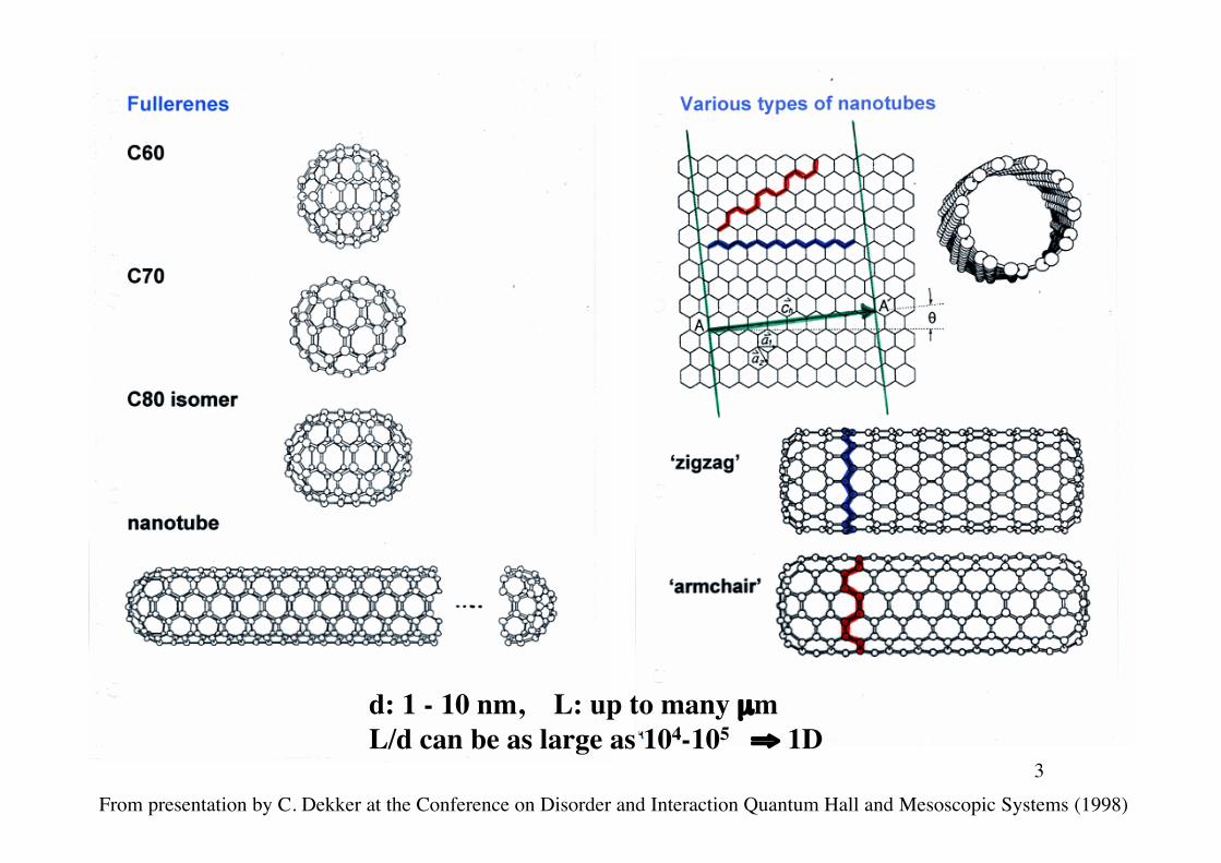
Fullerence & CNT
From presentation by C. Dekker at the Conference on Disorder and Interaction Quantum Hall and Mesoscopic Systems (1998)
d: 1 - 10 nm, L: up to many µmL/d can be as large as 104-105 ⇒ 1D

4
History of CNT and C60
From presentation by D. Zhang & C-L Lin, Carbon Nanotubes (2003)
5
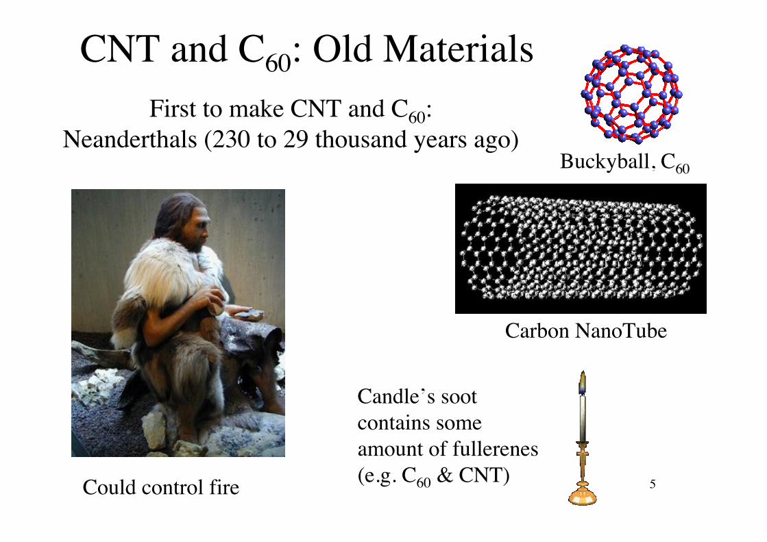
CNT and C60: Old MaterialsFirst to make CNT and C60:
Neanderthals (230 to 29 thousand years ago)
Carbon NanoTube
Buckyball, C60
Candle’s sootcontains someamount of fullerenes(e.g. C60 & CNT)Could control fire

6
Contents• Fullerenes
– Structure of e.g. C60 & Carbon Nanotubes (CNT)– History
• Metals, Semiconductors & Insulators– Band Gaps & Fermi Level– Graphite is Semimetal, SWNT: Metals or Semiconductors
• Single-Wall NanoTubes (SWNT)– Vector Notation, Atomic Structure– Electronic Structure– Magnetic Magic
• Electronic Transport in SWNT– Metallic & Semiconducting SWNT– Field Effect Transistor
• Summary

7
Band Gaps & Fermi Level of Materials
Britney's Guide to Semiconductor Physics, britneyspears.ac
Conduction band - The first unfilled energy level at T = 0 K (LUMO for molecules)Valence band - The last filled energy level at T = 0 K (HOMO for molecules)

8
Fermi-Level & Doping ofSemicontuctors
B.V. Zeghbroeck, Principles of Semiconductor Devices, Colarado University, ece-www.colorado.edu/~bart/
Fermi-Dirac Distribution Changes with T
Doping of Semiconductors

9
Metal, Semiconductor and Semimetal
P.G. Collins & P. Avouris, Nanotubes for Electronics, Scientific American (2000)
Metals:Conduct electricityeasily because many e-
have easy access toadjacent conductionstates
Semiconductors:e- need an energy boostfrom light or anelectrical field to jumpthe gap to the firstavailable conductionstate
Graphite:Semimetal that justbarely conducts. Only afew electrons can accessthe narrow path to aconduction state

10
SWNT: Metals or Semiconductors
a) armchair (5,5) nanotubeb) zigzag (9,0) nanotube
Infinitesimally small amountof energy is needed to excitean electron into an emptyexcited state
⇒ metallic
c) zigzag (10,0) nanotube
A finite band gap between theoccupied and empty states⇒ semicontucor
A small increase in diameterhas a major impact on theconduction properties ofcarbon nanotubes.
physicsweb.org
Electronic Energy varies with the Wavevector
Fermi level = 0

11
Contents• Fullerenes
– Structure of e.g. C60 & Carbon Nanotubes (CNT)– History
• Metals, Semiconductors & Insulators– Band Gaps & Fermi Level– Graphite is Semimetal, SWNT: Metals or Semiconductors
• Single-Wall NanoTubes (SWNT)– Vector Notation, Atomic Structure– Electronic Structure– Magnetic Magic
• Electronic Transport in SWNT– Metallic & Semiconducting SWNT– Field Effect Transistor
• Summary

12
Vector Notation
metal semiconductorM.S. & G. Dresselhaus, P. Avouris,Carbon Nanotubes, Springer (2001)
Rule: n - m = 3i⇒ Metallic if i is integer⇒ Semicontuctor if i is non-integer
Chiral vector: Ch = OA = na1 + ma2 ≡ (n,m)(n, m are integers, 0 ≤ |m| ≤ n)a1 & a2 are unit vektors
Chiral angle θ is defined as theangle between the vectors Ch anda1, with 0 ≤ |θ| ≤ 30° because of thehexagonal symmetry of thehoneycomb lattice

13
armchair(n,n)θ = 30˚
zigzag(n,0)θ = 0˚
chiral(n,m)0 < θ < 30˚
Structure of SWNTDirection of the 6-membered ring can be takenalmost arbitrarily. No distortion of the hexagons.Only distortion due to the curvature of the CNT.
hemisphere
R. Saito, G. & M.S. Dresselhaus, Physical Properties of Carbon Nanotubes, Imperial College Press (2003)
Chiral molecule:Not identical to itsmirror imageCannot be mapped toits mirror image byrotations andtranslations alone
na1 + ma2 ≡ (n,m)

14
DOS (sestekki)
Tutorial on Electronic Transport, Jesper Nygaard, Niels Bohr Institude, University of Copenhagen
DOS:number ofavailable statesper unit volumeper unit energy

15
Electronic StructureSTM of Metallic & Semiconducting CNT
Cees Dekker, Physics Today (1999)

16
Magnetic Magica) Magnetic field introduces a phase
factor to the electron wavefunctionin the circumferential direction.As a result, the electronicproperties of a nanotube can bemodulated by a magnetic field.
b) The energy spectrum is a plot ofenergy (E) versus wavevector (k).As the magnetic flux increases theenergy-band structure of thenanotube oscillates from that of ametal to that of a semiconductor.
J.Kong, L.Kouwenhoven & C. Dekker, Quantum change for nanotubes, Physics in Action (2004)

17
Contents• Fullerenes
– Structure of e.g. C60 & Carbon Nanotubes (CNT)– History
• Metals, Semiconductors & Insulators– Band Gaps & Fermi Level– Graphite is Semimetal, SWNT: Metals or Semiconductors
• Single-Wall NanoTubes (SWNT)– Vector Notation, Atomic Structure– Electronic Structure– Magnetic Magic
• Electronic Transport in SWNT– Metallic & Semiconducting SWNT– Field Effect Transistor
• Summary
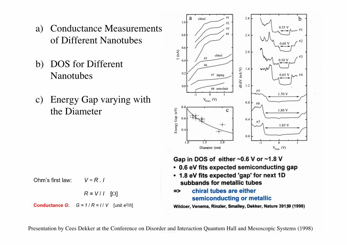
18Presentation by Cees Dekker at the Conference on Disorder and Interaction Quantum Hall and Mesoscopic Systems (1998)
a) Conductance Measurementsof Different Nanotubes
b) DOS for DifferentNanotubes
c) Energy Gap varying withthe Diameter

19Presentation by Cees Dekker at the Conference on Disorder and Interaction Quantum Hall and Mesoscopic Systems (1998)

20
Field Effect Transistor
Presentation by Cees Dekker at the Conference on Disorder and Interaction Quantum Hall and Mesoscopic Systems (1998)
21
Summary• The vector notation, atomic structure and the electronic
structure of SWNT has been explained.• SWNT are either chiral or achiral molecules and the cirality
of the nanotubes affects the properties.• SWNT can either have metallic properties or semiconducting
properties. That can be seen by both calculations andexperiments of the Density of State around the Fermi level.
• Magnetic field can change conduction properties of SWNT,varying them from being metallic to semiconducting and viceversa.
• It is possible to use SWNT to make a Field Effect Transistor.By applying a different gate voltage, one can change theconduction by many orders of magnitude. Carbon nanotubescould be used in molecular electronics in the future.