mems
DESCRIPTION
MEMSTRANSCRIPT

JOURNAL OF MICROELECTROMECHANICAL SYSTEMS, VOL. 24, NO. 5, OCTOBER 2015 1409
Fabrication of 3-D Silicon MicroneedlesUsing a Single-Step DRIE Process
Nima Rouhi, Cecile Jung-Kubiak, Victor White, Daniel Wilson, John Anderson,Colleen Marrese-Reading, and Siamak Forouhar
Abstract— Fabrication of 3-D microstructures is one ofthe most challenging aspects of silicon micromachining.In this paper, we present a novel microfabrication methodusing one single-step deep reactive ion etching process withgray-scale e-beam lithography mask that offers deeply etched(>350-µm deep) dual-angle 3-D microneedles with control overthe height and shape of the structures. Moreover, we foundthat the shape of the e-beam lithography patterns can determinethe general configuration and features of the final etchedmicroneedles, and that the etching process parameters havethe most impact on the microneedles’ shape, such as size andvertical base angle. Large arrays of 20 × 20 microneedles withheight uniformity of better than 3% are fabricated. [2014-0209]
Index Terms— 3D etch, silicon micro-structure, deep reactiveion etching, dual-angle, gray-scale e-beam lithography.
I. INTRODUCTION
THE CAPABILITY to create and more importantlycontrol the shape of three dimensional micro-structures
opens up a broad range of new applications in the futureof micro/nano-devices technology. Complex geometricalconfigurations are required in applications such as verticalvias for integrated circuits and packaging technology [1],micro-needles for biomedical and surgical devices [2], [3],lasers and photonic crystals [4], [5], battery industry [6], [7],micro-probes and cantilevers [8], micro-fluidics andmicro/nano-channels [9], [10], and chromatography [11].Three dimensional micro-structures play a criticalrole in the future of micro/nano-electromechanicalsystems (MEMS/NEMS) technology, yet convenientfabrication methods of high aspect ratio, 3D micro-needleswhile controlling the size and final configuration of themicro-patterns (using mask design and process control) arenot explored in depth.
Manuscript received July 14, 2014; revised January 30, 2015; acceptedFebruary 11, 2015. Date of publication March 5, 2015; date of current versionSeptember 29, 2015. This work was supported in part by the Jet PropulsionLaboratory, California Institute of Technology, Pasadena, CA, USA, undera contract with the National Aeronautics and Space Administrationunder Grant 105571, and in part by the U.S. Government Sponsorship.Subject Editor R. Maboudian.
N. Rouhi is with the Jet Propulsion Laboratory and the Departmentof Electrical Engineering, California Institute of Technology, Pasadena,CA 91125 USA (e-mail: [email protected]; [email protected]).
C. Jung-Kubiak, V. White, D. Wilson, J. Anderson, C. Marrese-Reading,and S. Forouhar are with the Jet Propulsion Laboratory, California Institute ofTechnology, Pasadena, CA 91125 USA (e-mail: [email protected];[email protected]; [email protected]; [email protected]; [email protected]; [email protected]).
Color versions of one or more of the figures in this paper are availableonline at http://ieeexplore.ieee.org.
Digital Object Identifier 10.1109/JMEMS.2015.2406878
A variety of methods have been studied to date to create3D MEMS structures. In general, there are either mask-basedor etch-based techniques, or a combination of both, thatresult in final three dimensional structures. One of the basicmethods of creating 3D shapes is using photoresist (PR)re-flow process to make masks and then transferringthat pattern into silicon [12], [13]. Despite the simpleand compatible nature of the re-flow mask process, itlacks the precise control over the patterns and fine/sharpfeatures on the mask which limits the number of possibleconfigurations.
One method uses difference in etch selectivity ofion-implanted (e.g. Gallium-implanted) silicon vs bulksilicon [14]. However, this process is complex and themaximum aspect ratio that can be achieved is small. This leadsto silicon features that are only a few micrometers in height.The combination of multiple etching processes, typically amixture of anisotropic and isotropic etch, is another process-based method of fabricating 3D structures [6], [8], [15]–[18].Most of these techniques require several etching steps (eitherdry etch or wet etch using KOH or a combination of both dryand wet etch) and also multiple lithography and/or alignmentprocedures. Furthermore, the degree of control over the shapeand angle (especially in wet etch) of the final structure usingthis combination process approach remains a problem yet tobe addressed in detail.
Given the limitations of the approaches described above, themost promising pathway for 3D MEMS fabrication is to usegray-scale lithography [19]–[22]. In gray-scale lithography,the radiation flux intensity is carefully controlled at differentlocations on a sample coated with photosensitive material tocreate a 3D mask shape. The radiation flux intensity is con-trolled either by altering the e-beam or UV dose/intensity inmaskless lithography [23]–[25], or by varying the transparencyof the mask on a contact mask [20], [26]–[28]. Because of thepower of this technique, there have recently been numerousdevelopments in mask design and gray-scale lithography tomake 3D micro-patterns. However, despite these efforts, theprogress on transferring those 3D patterns into bulk silicon isstill not explored in depth, especially for making high aspectratio structures and controlling the shape of deeply-etchedfeatures.
In this work, we demonstrate a novel method to fabricatehigh aspect ratio, vertical 3D silicon micro-needlesusing e-beam lithography and one-step DRIE of silicon.E-beam lithography masks are written in Polymethyl-glutarimide (PMGI), and the PR patterns are transferred into
1057-7157 © 2015 IEEE. Personal use is permitted, but republication/redistribution requires IEEE permission.See http://www.ieee.org/publications_standards/publications/rights/index.html for more information.
1410 JOURNAL OF MICROELECTROMECHANICAL SYSTEMS, VOL. 24, NO. 5, OCTOBER 2015
TABLE I
MASK DESIGN DETAILS, EACH ANGLE HERE DEFINES
A DIFFERENT PATTERN SHAPE (FIG. 1)
thermal oxide to be used as the etching mask for the DRIEof silicon. The presented 3D silicon micro-structures havea dual-angle shape with different heights and also sharpfeatures (grooves) designed in the body of the structures.More details of the mask design and e-beam writing as wellas patterns transfer and silicon etching are discussed in thefollowing sections.
II. PREPARATION OF THREE-DIMENSIONAL MASKS
1 mm thick <100> silicon wafers are used as the corematerial for forming the 3D structures. These wafers includea thermal oxide layer of 2.5µm. Microchem’s PMGI SF-9e-beam sensitive resist is spin coated on top of the oxide layer.Multiple thin coatings of the resist are used to reach 4 µm totalthickness. Based on our gray-scale lithography PR exposureand development, this initial 4 µm PMGI thickness is requiredto achieve the final 2.5 ∼ 3 µm PMGI after the e-beamlithography. The e-beam lithography patterns in PMGI are thentransferred into the silicon oxide for the final mask beforeetching the silicon.
A. Mask Design
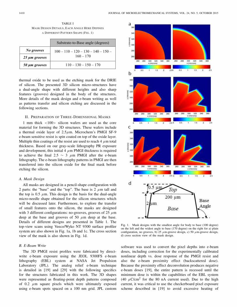
All masks are designed in a pencil-shape configuration with2 parts: the “base” and the “top”. The base is 2 µm tall andthe top is 0.5 µm. This design is the basis for the dual-anglemicro-needle shape obtained for the silicon structures whichwill be discussed later. Furthermore, to explore the transferof small features onto the silicon, the masks are designedwith 3 different configurations: no-grooves, grooves of 25 µmdeep at the base and grooves of 50 µm deep at the base.Details of different designs are presented in Table 1. Thetop-view scans using Veeco/Wyko NT 9300 surface profilersystem are also shown in Fig. 1a, 1b and 1c. The cross sectionview of the mask is also shown in Fig. 1d.
B. E-Beam Write
The 3D PMGI resist profiles were fabricated by direct-write e-beam exposure using the JEOL 9300FS e-beamlithography (EBL) system at NASA Jet PropulsionLaboratory (JPL). The analog relief e-beam techniqueis detailed in [19] and [29] with the following specificsfor the structures fabricated in this work. The 3D shapeswere represented as floating-point depth patterns composedof 0.2 µm square pixels which were ultimately exposedusing e-beam spots spaced on a 100 nm grid. JPL custom
Fig. 1. Mask designs with the smallest angle for body to base (100 degree)on the left and the widest angle to base (170 degree) on the right for a) plainconfiguration, no grooves, b) 25 µm-groove design, c) 50 µm-groove design,d) cross section view of the mask design.
software was used to convert the pixel depths into e-beamdoses, including correction for the experimentally calibratednonlinear depth vs. dose response of the PMGI resist andalso the e-beam proximity effect (backscattered dose).Because the proximity effect deconvolution produces negativee-beam doses [19], the entire pattern is recessed until theminimum dose is within the capabilities of the EBL system(40 µC/cm2 for the 80 nA current used). Due to the highcurrent, it was critical to use the checkerboard pixel exposurescheme described in [19] to avoid excessive heating of

ROUHI et al.: FABRICATION OF 3-D SILICON MICRONEEDLES USING A SINGLE-STEP DRIE PROCESS 1411
Fig. 2. E-beam Mask Transfer. In all a, b, c, rows in this figure the left column shows the 3D scan image of PMGI SF9 resist after e-beam lithography,middle column is the 3D scan of the transferred pattern into oxide mask after F-ICP RIE, and the right column shows the top-view optical image of the oxidemask shown in the middle column, a) Plain (no-groove) configuration, b) 25 µm, and c) 50 µm grooves.
the PMGI. This was accomplished using JPL softwarethat converts the corrected analog dose pixel patterns intonative binary pattern files for the JEOL EBL system. Afterexposure with a 100keV beam, the resist was developed inan iterative manner using MicroChem 101A developer withdepth measurement between steps to achieve accurate profilesfor the 3D shapes.
C. Resist Pattern Transfer to Oxide Mask
After e-beam lithography and development, the patternsare transferred into the 2.5 µm thermal oxide. This step isdone in a Unaxis Fluorine ICP (inductively coupled plasma)RIE (reactive ion etching) system with O2, Ar, and CHF3 asthe input gases. The etch process is adjusted so that the etchselectivity between oxide:PMGI is ∼1:1.1, therefore, at theend of the etch time, the PMGI pattern is fully transferred intothe oxide and no resist is left at the top. Interferometry scansof all 3 designs for the PMGI patterns, the oxide patterns,along with the top-view optical image of each shape aredemonstrated in Fig. 2.
III. EXPERIMENTS AND RESULTS
Silicon dioxide is used as a mask for silicon etchingdue to its amorphous structure (no etch direction preference
because of crystal orientation) and temperature stability inDRIE processes, which gives higher etch selectivity comparedto photoresist mask resulting in high aspect ratio siliconstructures.
A. Etch Process Parameters
Following the oxide mask preparation, samples are etchedusing a Plasma-Therm DRIE machine. The DRIE processconsists of cycles of 3 steps: 1- depositing the polymer toprotect the sidewalls, 2- etching the polymer at the bottomto create opening for Si removal, and 3- etching the silicon.The selectivity between oxide and silicon (Ox:Si) forour process and patterns configuration is found to beapproximately 1:150.
Each parameter of the process such as pressure, gas ratios,and timing of the each step of cycles was optimized tocreate silicon micro structures with sidewall angles about90 degree from the substrate. During the process, the chamberpressure is changing from 15 mTorr to 40 mTorr (variationfor each step of the cycle) and plasma powers are in therange of 1500W to 3300W. For step 1 (polymer deposition)C4F8 and Ar are inserted into the chamber and forsteps 2 and 3 (polymer etch and silicon etch) SF6 and Arare introduced into the chamber.

1412 JOURNAL OF MICROELECTROMECHANICAL SYSTEMS, VOL. 24, NO. 5, OCTOBER 2015
Fig. 3. SEM images of the DRIE process over time, after a) 45 min,b) 65 min, and c) 80 min, for the design with 25 µm grooves.
While working on the timing of each 3 steps, we realizedthat decreasing the timing for the polymer deposition-step(step 1), while keeping the rest of the parameters unchanged,will result in obvious undercut. On the other hand, decreasingthe etch-step (step 3) timing will result in grass formationat the bottom of the sample due to non-sufficient timing tocompletely remove the polymer residues. Extensive effortswere put to find the optimum timing of each step and thebest operating pressure, to keep the base angle as vertical aspossible while minimizing the grass formation on the siliconneedles.
B. E-Beam Lithography Sample Etch
After optimization of the DRIE process, we etched the 3Doxide masks presented in section II. The different substrate-to-base angles designed and presented in Table 1 help to elucidatethe impact of the mask shape and the transfer of the e-beam
Fig. 4. SEM images of the final silicon micro-needles for all ofthe 3 proposed e-beam lithography masks, with a) plain (no-groove)configuration, b) 25 µm, and c) 50 µm grooves (the optical image of thestarting oxide mask for each micro-needle is shown in the inset of theSEM images).
written features on the final structure. Furthermore, due to thepre-defined dual-angle masks, the silicon needles will have apencil shape with dual-angle as well while using only a single-step DRIE process. The “base” part of the mask will form thebody of the silicon pillar while the “top” of the mask shapesthe tip of the silicon pillar.
Fig. 3 shows SEM (scanning electron microscopy) imagesof the silicon micro-needles at different times during theDRIE process. The images illustrate the smooth transition fromstraight pillar to dual-angle needle, following the pre-defineddual-angle oxide mask.
However, regardless of the mask’s substrate-to-baseangles (ranging from 100 - 170 degrees), the final siliconmicro-needles fabricated have very similar base angles witha slight improvement (increase in base angle) for wider

ROUHI et al.: FABRICATION OF 3-D SILICON MICRONEEDLES USING A SINGLE-STEP DRIE PROCESS 1413
TABLE II
ANALYSIS OF THE SILICON MICRO-NEEDLES AFTER DRIE
PROCESS, IN HEIGHT AND SURFACE-TO-BASE ANGLES
(ON A SAMPLE OF 34 STRUCTURES)
mask base angles. As the etching process was optimizedfor vertical structures, it is believed that a modification ofthe etch process parameters would have more impact on thebase angle, rather than the e-beam mask’s substrate-to-baseangle.
Further analysis of the silicon structures shows a variationfrom 86.2 - 89 degree over a selection of 34 micro-needles,with ∼60% of them above 88 degree. Height analysis ofthe silicon structures shows a variation of ±2.6% in height(371.4 - 391.3 µm) over the selection of 34 micro-needleswith more than 67% of them within ±1% of the average height(384 µm). Table 2 shows a summary of those analyses.
We finally analyzed the transfer function of the e-beamwritten features onto the silicon, using the 3 e-beam designswith different groove depths. Fig. 4 shows that for oursingle-step DRIE process, we have the capabilities to fullytransfer all the details of the mask into the bulk silicon.As shown in Fig. 4c, the deepest groove design (50 µm deep)was transferred into the sidewall of the micro-needle allthe way to the bottom of the etched micro-needle. With theoptimized DRIE process, no grass formation is observedinside the silicon grooves or at the transition of sidewall – tip.
IV. CONCLUSION
Silicon 3D micro-needles with dual-angle pencil-shapewere fabricated and analyzed. Gray-scale e-beam lithographywas used to create a unique 3D mask in PMGI resist, witha pre-defined dual-angle. The patterns were then transferredinto silicon oxide layer by developing a controlled selectivitybetween PMGI and oxide. The final and most important stepof the process was developing a single-step DRIE process tocreate the high aspect ratio, dual-angle 3D needle-shapemicro-structures as opposed to previously reportedmicro-needles fabricated using multiple-processing steps.Moreover, using the gray scale e-beam lithography offersthe possibility to add features to the masks, such as grooves,that can be finely and fully transferred into the siliconmicro-structures. Furthermore, this work shows that althoughthe shape of e-beam lithography patterns can determinethe general configuration and features of the final etchedmicro-needles, the etching process has the most impact ontransferring the details such as size and base angle, with
extensive effort put on controlling the verticality of the etchedstructures.
Here, we developed and presented a 3D transfer processfrom gray-scale mask design to silicon oxide and finally intothe bulk silicon, to control the final configuration and shape ofa silicon micro-needle. In addition, the height of our samples(∼400 µm) opens up a significant number of opportunitiesfor electrical, mechanical, and biological applications. Thedual-angle configuration makes these micro-needles suitablefor biomedical and hypodermic injection applications. Finally,the grooves designed in the 3D masks also ensure the abilityof this process to integrate and transfer small features ina 3D silicon micro-structure.
ACKNOWLEDGMENT
The authors would also like to thank Dr. Frank Greer forinsightful discussions before publication.
REFERENCES
[1] D. S. Tezcan et al., “Development of vertical and tapered via etch for 3Dthrough wafer interconnect technology,” in Proc. 8th Electron. Packag.Technol. Conf. (EPTC), Dec. 2006, pp. 22–28.
[2] F. Chabri et al., “Microfabricated silicon microneedles for nonvi-ral cutaneous gene delivery,” Brit. J. Dermatol., vol. 150, no. 5,pp. 869–877, May 2004.
[3] Y.-C. Kim, J.-H. Park, and M. R. Prausnitz, “Microneedles for drug andvaccine delivery,” Adv. Drug Del. Rev., vol. 64, no. 14, pp. 1547–1568,Nov. 2012.
[4] J. Schilling, F. Müller, S. Matthias, R. B. Wehrspohn, U. Gösele, andK. Busch, “Three-dimensional photonic crystals based on macroporoussilicon with modulated pore diameter,” Appl. Phys. Lett., vol. 78, no. 9,pp. 1180–1182, Feb. 2001.
[5] S. Balslev, T. Rasmussen, P. Shi, and A. Kristensen, “Single mode solidstate distributed feedback dye laser fabricated by gray scale electronbeam lithography on a dye doped SU-8 resist,” J. Micromech. Microeng.,vol. 15, no. 12, pp. 2456–2460, Dec. 2005.
[6] J. L. Goldman, B. R. Long, A. A. Gewirth, and R. G. Nuzzo, “Strainanisotropies and self-limiting capacities in single-crystalline 3D siliconmicrostructures: Models for high energy density lithium-ion batteryanodes,” Adv. Funct. Mater., vol. 21, no. 13, pp. 2412–2422, Jul. 2011.
[7] M. Nathan et al., “Three-dimensional thin-film Li-ion microbatteriesfor autonomous MEMS,” J. Microelectromech. Syst., vol. 14, no. 5,pp. 879–885, Oct. 2005.
[8] S. Park et al., “A novel 3D process for single-crystal silicon micro-probe structures,” J. Micromech. Microeng., vol. 12, no. 5, pp. 650–654,Sep. 2002.
[9] O. J. Hildreth, W. Lin, and C. P. Wong, “Effect of catalyst shape andetchant composition on etching direction in metal-assisted chemicaletching of silicon to fabricate 3D nanostructures,” ACS Nano, vol. 3,no. 12, pp. 4033–4042, Dec. 2009.
[10] V. Nock and R. J. Blaikie, “Fabrication of optical grayscale masks fortapered microfluidic devices,” Microelectron. Eng., vol. 85, nos. 5–6,pp. 1077–1082, May/Jun. 2008.
[11] T. B. Kirchner, N. A. Hatab, N. V. Lavrik, and M. J. Sepaniak, “Highlyordered silicon pillar arrays as platforms for planar chromatography,”Anal. Chem., vol. 85, no. 24, pp. 11802–11808, Dec. 2013.
[12] D. A. Fletcher et al., “Microfabricated silicon solid immersion lens,”J. Microelectromech. Syst., vol. 10, no. 3, pp. 450–459, Sep. 2001.
[13] S. Audran, B. Mortini, B. Faure, and G. Schlatter, “Dynamical forma-tion of microlenses by the reflow method: Numerical simulation andexperimental study of the process fabrication,” J. Micromech. Microeng.,vol. 20, no. 9, p. 095008, Sep. 2010.
[14] H. X. Qian, W. Zhou, J. Miao, L. E. N. Lim, and X. R. Zeng,“Fabrication of Si microstructures using focused ion beam implantationand reactive ion etching,” J. Micromech. Microeng., vol. 18, no. 3,p. 035003, Mar. 2008.
[15] T. Bourouina, T. Masuzawa, and H. Fujita, “The MEMSNAS process:Microloading effect for micromachining 3-D structures of nearly allshapes,” J. Microelectromech. Syst., vol. 13, no. 2, pp. 190–199,Apr. 2004.

1414 JOURNAL OF MICROELECTROMECHANICAL SYSTEMS, VOL. 24, NO. 5, OCTOBER 2015
[16] Z. P. Huang, N. Geyer, P. Werner, J. de Boor, and U. Gösele, “Metal-assisted chemical etching of silicon: A review,” Adv. Mater., vol. 23,no. 2, pp. 285–308, Jan. 2011.
[17] F. Chamran, Y. Yeh, H.-S. Min, B. Dunn, and C.-J. Kim, “Fabrication ofhigh-aspect-ratio electrode arrays for three-dimensional microbatteries,”J. Microelectromech. Syst., vol. 16, no. 4, pp. 844–852, Aug. 2007.
[18] Y. Yao, M. N. Gulari, J. A. Wiler, and K. D. Wise, “A microassembledlow-profile three-dimensional microelectrode array for neural prosthesisapplications,” J. Microelectromech. Syst., vol. 16, no. 4, pp. 977–988,Aug. 2007.
[19] D. W. Wilson, R. E. Muller, P. M. Echternach, and J. P. Backlund,“Electron-beam lithography for micro- and nano-optical applications,”Proc. SPIE, vol. 5720, pp. 68–77, Apr. 2005.
[20] C. M. Waits, B. Morgan, M. Kastantin, and R. Ghodssi, “Microfabri-cation of 3D silicon MEMS structures using gray-scale lithography anddeep reactive ion etching,” Sens. Actuators A, Phys., vol. 119, no. 1,pp. 245–253, Mar. 2005.
[21] K. Totsu and M. Esashi, “Gray-scale photolithography using masklessexposure system,” J. Vac. Sci. Technol. B, vol. 23, pp. 1487–1490,Jul./Aug. 2005.
[22] L. Mosher, C. M. Waits, B. Morgan, and R. Ghodssi, “Double-exposuregrayscale photolithography,” J. Microelectromech. Syst., vol. 18, no. 2,pp. 308–315, Apr. 2009.
[23] F. Hu and S.-Y. Lee, “Dose control for fabrication of grayscale structuresusing a single step electron-beam lithographic process,” J. Vac. Sci.Technol. B, vol. 21, no. 6, pp. 2672–2679, Nov./Dec. 2003.
[24] J. C. Galas, B. Belier, A. Aassime, J. Palomo, D. Bouville, and J. Aubert,“Fabrication of three-dimensional microstructures using standard ultra-violet and electron-beam lithography,” J. Vac. Sci. Technol. B, vol. 22,no. 3, pp. 1160–1162, May/Jun. 2004.
[25] A. Schleunitz and H. Schift, “Fabrication of 3D nanoimprint stamps withcontinuous reliefs using dose-modulated electron beam lithography andthermal reflow,” J. Micromech. Microeng., vol. 20, no. 9, p. 095002,Sep. 2010.
[26] C.-K. Wu, “Surface treated silver ion exchanged glass,”U.S. Patent 5 078 771, Jan. 7, 1992.
[27] S.-I. Chang and J.-B. Yoon, “Shape-controlled, high fill-factor microlensarrays fabricated by a 3D diffuser lithography and plastic replicationmethod,” Opt. Exp., vol. 12, no. 25, pp. 6366–6371, Dec. 2004.
[28] M. Christophersen and B. F. Phlips, “Gray-tone lithography using anoptical diffuser and a contact aligner,” Appl. Phys. Lett., vol. 92, no. 19,p. 194102, May 2008.
[29] D. W. Wilson, P. D. Maker, R. E. Muller, P. Z. Mouroulis, andJ. Backlund, “Recent advances in blazed grating fabrication by electron-beam lithography,” Proc. SPIE, vol. 5173, pp. 115–126, Nov. 2003.
Nima Rouhi received the B.Sc. andM.Sc. degrees from the Department of ElectricalEngineering, University of Tehran, Tehran, Iran,in 2005 and 2007, respectively, and the Ph.D. degreefrom the Department of Electrical Engineeringand Computer Science, University of California,Irvine, CA, USA, in 2011. He joined NovartisResearch and Development Laboratories as aMEMS Engineer until summer 2013. Since 2013,he has been a Post-Doctoral Scholar with theCalifornia Institute of Technology, where he was
involved in the NASA Project with the NASA Jet Propulsion Laboratory.He has co-authored over 30 journal papers and international conferenceproceedings, and over 10 invited talks and presentations. His researchworks were also highlighted by several news and media, including IEEESPECTRUM and the Association for Computing Machinery Communications.
Cecile Jung-Kubiak received the Master’s degreein physics and materials chemistry fromPolytech’Montpellier, France, in 2006, andthe Ph.D. degree in physics from UniversiteParis-Sud XI, France, in 2009. She is currentlya member of the Technical Staff of theS.W.A.T. Group with the Jet Propulsion Laboratory,Pasadena, CA, USA. She has co-authoredover 40 papers in international journals andconferences, and holds several patents. Her researchinterests include the development of 3-D silicon
micromachining technologies using DRIE techniques, the miniaturizationof multipixel arrays to build compact 3-D instruments, and GaAs-basedfrequency multipliers and mixers in the THz region. She was a recipient ofa 2-year NASA Post-Doctoral Fellowship with the California Institute ofTechnology in 2010. She was also a recipient of the 2010 JPL OutstandingPost-Doctoral Research Award in the field Technology, Instrumentation, andEngineering, and the 2014 IEEE THz Science and Technology Best PaperAward.
Victor White, photograph and biography not available at the time ofpublication.
Daniel Wilson, photograph and biography not available at the time ofpublication.
John Anderson received the Ph.D. degree inmechanical engineering from Colorado State Univer-sity, in 1992. He has been with the Jet PropulsionLaboratory since 1992, where he has been involvedin a variety of flight and research projects. His activ-ities have included design, modeling, and testing ofdevices for electrospray applications.
Colleen Marrese-Reading received theBachelor’s degree in engineering physics in 1994,and the Master’s and Ph.D. degrees in aerospaceengineering from the University of Michigan,in 1999. She is currently a Senior Engineer ofthe Jet Propulsion Laboratory with the ElectricPropulsion Group. She is also the PrincipalInvestigator on the development of an electrospraythruster technology with microfabricated arrays ofsilicon needles. She has co-authored over 25 papersin journals and conferences, and holds multiple
patents.
Siamak Forouhar, photograph and biography not available at the time ofpublication.