memory (cont.) perspectives
TRANSCRIPT

1
EE141 – Fall 2005Lecture 26
Memory (Cont.)Memory (Cont.)PerspectivesPerspectives
EE141 2
Administrative Stuff
Homework 10 posted – just for practice• No need to turn in
Office hours next week, schedule TBD.
HKN review today. Your feedback is important!
Final covers all material covered in class. Precise overview to be posted on web-site.
Review session schedule TBD.

2
EE141 3
Project 2 – Summary
Variety of topologies and circuit styles• Most projects focused on mix of static logic families
Some very impressive presentations• Refer to examples on web-site
Grades• Mean: 79.3 • Median: 78.9 (3.868, static)• Sigma: 19• Max: 110 (0.944, dynamic; 1.316, static)
EE141 4
Sizing Optimization
16X
Stage Z: LE=1 B=1
3
3.84u/1.92u
960n960n
2.88u/720n
2.4u/1.2u
0.96n0.96n1.2u 0.96n
0.48u
0.48u
16XGin7Gin5Gin0 Gin1 Gin2 Gin3 Gin4 Gin6
Pin7Pin1 Pin2 Pin5Pin3 Pin4 Pin6
Pin0
A
Stage V: LE=1, B=1
Stage W: LE=1, B=4
Stage X : LE=4/3, B=1
Stage Y: LE=2, B=1
Area Concern
0.96u/0.48u
163812
3411
=
=××××=
FO
LE
8.241638
4:5/1
5/1 =
××=PE
Branching 00.1=v78.2=w 08.4=y
70.5=z
94.1=xSize: 2.5
4
2.5
Manchester Sizing

3
EE141 5
Layout Techniques
Size : 1265.22 µm2
(33.00µm x 38.34µm)
Critical Path drawn in arrow
Aspect Ratio = 1.162
Routing• Metal 1
− Horizontal Line− VDD, GND
• Metal 2:− Vertical Line
• Metal 3:− Clock Signals
FA0 FA1 FA2 FA3
FA7 FA6 FA5 FA4
INPUT BUFFER INPUT BUFFER
INPUT BUFFER INPUT BUFFER
OUTPUTBUFFER
OUTPUTBUFFER
OUTPUTBUFFER
OUTPUTBUFFER
CLOCKCHAIN
MemoryMemory

4
EE141 7
Read-Write MemoryNon-VolatileRead-Write
MemoryRead-Only Memory
EPROM
E2PROM
FLASH
RandomAccess
Non-RandomAccess
SRAM
DRAM
Mask-Programmed
Programmable (PROM)
FIFO
Shift Register
CAM
LIFO
Semiconductor Memory Classification
EE141 8
Read-Only Memory Cells
WL
BL
WL
BL
1WL
BL
WL
BL
WL
BL
0
VDD
WL
BL
GND
Diode ROM MOS ROM 1 MOS ROM 2

5
EE141 9
WL[0]
GND
BL [0]
WL [1]
WL [2]
WL [3]
VDD
BL [1]
Pull-up devices
BL [2] BL [3]
GND
MOS NOR ROM
EE141 10
Programming using theActive Layer Only
Polysilicon
Metal1
Diffusion
Metal1 on Diffusion
Cell (9.5λ x 7λ)
MOS NOR ROM Layout

6
EE141 11
MOS NOR ROM Layout
Polysilicon
Metal1
Diffusion
Metal1 on Diffusion
Cell (11λ x 7λ)
Programming usingthe Contact Layer Only
EE141 12
All word lines high by default with exception of selected row
WL [0]
WL [1]
WL [2]
WL [3]
VDD
Pull-up devicesBL [3]BL [2]BL [1]BL [0]
MOS NAND ROM

7
EE141 13
No contact to VDD or GND necessary;
Loss in performance compared to NOR ROMdrastically reduced cell size
Polysilicon
Diffusion
Metal1 on Diffusion
Cell (8λ x 7λ)
Programming usingthe Metal-1 Layer Only
MOS NAND ROM Layout
EE141 14
Cell (5λ x 6λ)
Polysilicon
Threshold-alteringimplant
Metal1 on Diffusion
Programming usingImplants Only
NAND ROM Layout

8
EE141 15
PMOS precharge device can be made as large as necessary,but clock driver becomes harder to design.
WL [0]
GND
BL [0]
WL [1]
WL [2]
WL [3]
VDD
BL [1]
Precharge devices
BL [2] BL [3]
GND
pref
Precharged MOS NOR ROM
EE141 16
Read-Write MemoryNon-VolatileRead-Write
MemoryRead-Only Memory
EPROM
E2PROM
FLASH
RandomAccess
Non-RandomAccess
SRAM
DRAM
Mask-Programmed
Programmable (PROM)
FIFO
Shift Register
CAM
LIFO
Semiconductor Memory Classification

9
EE141 17
Non-Volatile MemoriesThe Floating-gate transistor (FAMOS)
Floating gate
Source
Substrate
Gate
Drain
n+ n+_p
tox
tox
Device cross-section Schematic symbol
G
S
D
EE141 18
0 V
- 5 V 0 V
DS
Removing programming voltage leaves charge trapped
5 V
- 2.5 V 5 V
DS
Programming results inhigher VT.
20 V
10 V 5 V 20 V
DS
Avalanche injection
Floating-Gate Transistor Programming

10
EE141 19
FLOTOX EEPROM
Floating gate
Source
Substratep
Gate
Drain
n1 n1
FLOTOX transistor Fowler-NordheimI-V characteristic
20–30 nm
10 nm
-10 V10 V
I
VGD
EE141 20
EEPROM Cell
WL
BL
VDD
Absolute threshold controlis hardUnprogrammed transistor might be depletion
2 transistor cell

11
EE141 21
EPROMFlashCourtesy Intel
Cross Sections of NVM Cells
EE141 22
Read-Write Memories (RAM)
Static (SRAM)• Data stored as long as supply is applied• Large (6 transistors/cell)• Fast• Differential
Dynamic (DRAM)• Periodic refresh required• Small (1-3 transistors/cell)• Slower• Single ended

12
EE141 23
WL
BL
VDD
M5M6
M4
M1
M2
M3
BL
6-Transistor CMOS SRAM Cell
EE141 24
WL
BL
VDD
M 5M 6
M 4
M1 VDDVDD VDD
BL
Q = 1Q = 0
Cbit Cbit
CMOS SRAM Analysis (Read)

13
EE141 25
CMOS SRAM Analysis (Read)
00
0.2
0.4
0.6
0.8
1
1.2
0.5
V o l t a g e r i s e [ V ]
1 1.2 1.5 2Cell Ratio (CR)
2.5 3
Vol
tage
Ris
e (V
)
EE141 26
BL = 1 BL = 0
Q = 0Q = 1
M1
M4
M5
M6
VDD
VDD
WL
CMOS SRAM Analysis (Write)

14
EE141 27
CMOS SRAM Analysis (Write)
EE141 28
VDD
GND
WL
BLBL
M1 M3
M4M2
M5 M6
WL
BL
VDD
M5M6
M4
M1
M2
M3
BL
6T-SRAM Layout

15
EE141 29
Static power dissipation -- Want RL largeBit lines precharged to VDD to address tp problem
M3
RL RLVDD
WL
Q Q
M1 M2
M4
BL BL
Resistive Load SRAM Cell
EE141 30
No constraints on device ratiosReads are non-destructiveValue stored at node X when writing a “1” = VWWL-VTn
WWL
BL1
M1 X
M3
M2
CS
BL2
RWL
VDD
VDD - VT
DVVDD - VTBL 2
BL 1
X
RWL
WWL
3-Transistor DRAM Cell

16
EE141 31
BL2 BL1 GND
RWL
WWL
M3
M2
M1
WWL
BL1
M1 X
M3
M2
CS
BL2
RWL
3T DRAM Layout
EE141 32
Write: CS is charged or discharged by asserting WL and BL.Read: Charge redistribution takes places between bit line and storage capacitance
Voltage swing is small; typically around 250 mV.
M1
CS
WL
BL
CBL
VDD2 VT
WL
X
sensing
BL
GND
Write 1 Read 1
VDD
VDD /2 VDD /2
∆V BL VPRE– VBIT VPRE–CS
CS CBL+------------= =V
1-Transistor DRAM Cell

17
EE141 33
Uses Polysilicon-Diffusion CapacitanceExpensive in Area
M1 wordline
Diffusedbit line
Polysilicongate
Polysiliconplate
Capacitor
Cross-section Layout
Metal word line
Poly
SiO2
Field Oxiden+ n+
Inversion layerinduced byplate bias
Poly
1T DRAM Cell
EE141 34
Micrograph of 1T DRAM

18
EE141 35
Cell Plate Si
Capacitor Insulator
Storage Node Poly
2nd Field Oxide
Refilling Poly
Si Substrate
Trench Cell Stacked-capacitor Cell
Capacitor dielectric layerCell plateWord line
Insulating Layer
IsolationTransfer gateStorage electrode
Advanced 1T DRAM Cells
Perspectives

19
EE141 37
EE141 Summary
Digital circuit designers will have jobs in 2010+
Major challenges• Cost• Power consumption• Robustness• Complexity
Some new circuit solutions and design methodologies are coming
EE141 38
Medium High Very HighVariability
Energy scaling will slow down>0.5>0.5>0.35Energy/Logic Op scaling
0.5 to 1 layer per generation8-97-86-7Metal Layers
11111111RC Delay
Reduce slowly towards 2-2.5<3~3ILD (K)
Low Probability High ProbabilityAlternate, 3G etc
32
11
2016
High Probability Low ProbabilityBulk Planar CMOS
Delay scaling will slow down>0.7~0.70.7Delay = CV/I scaling
641684210.5Integration Capacity (BT)
8162232456590Technology Node (nm)
2018201420122010200820062004
Internal University FCRP(MARCO)Courtesy: R. Krishnamurthy (Intel)
Technology Scaling

20
EE141 39
Research Roadmap
EE141 40
Device Evolution

21
EE141 41
25nm FinFET
25 nm MOS transistor (Folded Channel)
EE141 42
Cost
Mask cost in 90nm technology is over $1MBugs are very expensiveDesign effort increases in DSMCost of new toolsNon-recurring costs dominate the price effectiveness of low-volume ASICsNeed to have a product that can fit multiple applications, customers (flexibility)

22
EE141 43
Power has become a Problem
5KW 18KW
1.5KW 500W
400480088080
80858086
286386
486Pentium ®
0.1
1
10
100
1000
10000
100000
1971 1974 1978 1985 1992 2000 2004 2008Year
Pow
er (W
atts
)
Power delivery and dissipation will be prohibitivePower delivery and dissipation will be prohibitive
Source:S. Borkar(Intel)
Pentium Pro
EE141 44
The Productivity Gap
1
10
100
1,000
10,000
100,000
1,000,000
10,000,000
2003
1981
1983
1985
1987
1989
1991
1993
1995
1997
1999
2001
2005
2007
2009
10
100
1,000
10,000
100,000
1,000,000
10,000,000
100,000,000Logic Tr./ChipTr./Staff Month.
xxx
xxx
x21%/Yr. compound
Productivity growth rate
x
58%/Yr. compoundedComplexity growth rate
10,000
1,000
100
10
1
0.1
0.01
0.001
Logi
c Tr
ansi
stor
per
Chi
p(M
)
0.01
0.1
1
10
100
1,000
10,000
100,000
Prod
uctiv
ity(K
) Tra
ns./S
taff
-Mo.
Com
plex
ity
Complexity outpaces design productivityComplexity outpaces design productivity
Source: Sematech
Today

23
EE141 45
Some FPGA Examples
Xilinx Spartan-3 Xilinx IQ
EE141 46
µP
Prog Mem
MACUnit
AddrGenµP
Prog Mem
µP
Prog Mem
SatelliteProcessorDedicated
Logic
SatelliteProcessor
SatelliteProcessor
GeneralPurpose
µP
Software
DirectMapped
Hardware
HardwareReconfigurable
Processor
ProgrammableDSP
Flex
ibili
ty
Inefficiency
The Architectural Tradeoff Game
24
EE141 47
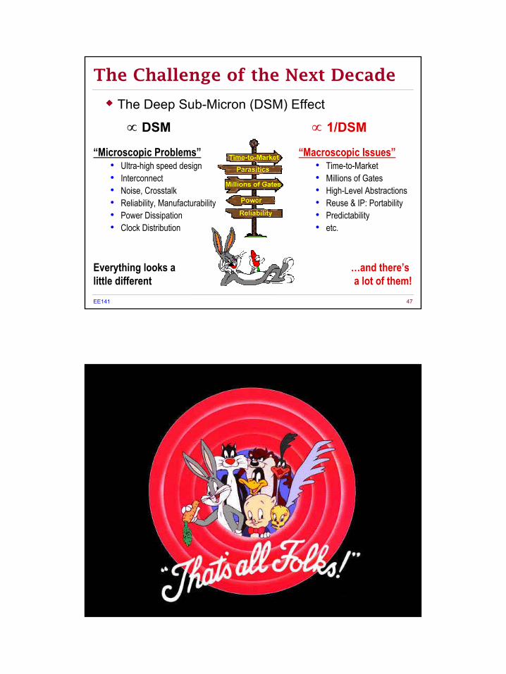
The Challenge of the Next Decade
∝ DSM ∝ 1/DSM
…and there’s a lot of them!
“Microscopic Problems”• Ultra-high speed design• Interconnect• Noise, Crosstalk• Reliability, Manufacturability• Power Dissipation• Clock Distribution
Everything looks a little different
The Deep Sub-Micron (DSM) Effect
“Macroscopic Issues”• Time-to-Market• Millions of Gates• High-Level Abstractions• Reuse & IP: Portability• Predictability• etc.
EE141 48