mem 0 mapnet: a three dimensional fabric for reliable …€¦ · · 2015-12-16design and layout...
TRANSCRIPT
1
ID 1
EX 3
MEM 1
WB 2
IF 0
CORE 3
IF 3
IF 2
IF 1
ID 0
ID 2
ID 3
EX 0
EX 1
EX 2
MEM 0
MEM 2
MEM 3
WB 0
WB 1
WB 3
CORE 2
CORE 1
CORE 0
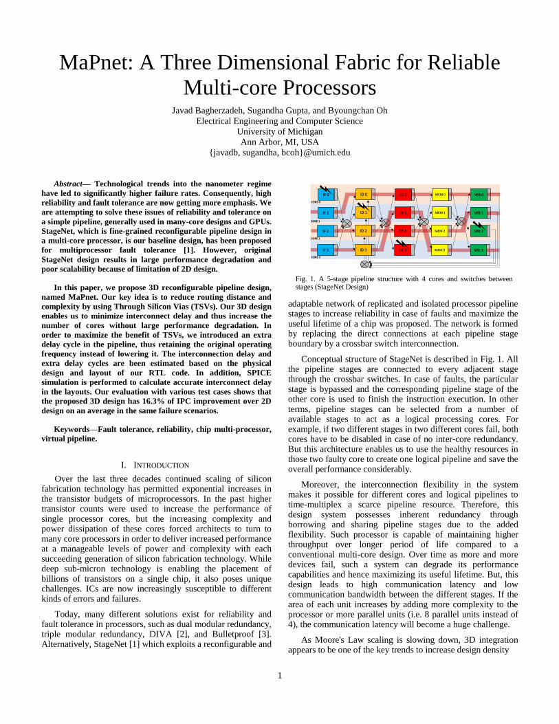
Fig. 1. A 5-stage pipeline structure with 4 cores and switches between stages (StageNet Design)
MaPnet: A Three Dimensional Fabric for Reliable
Multi-core Processors Javad Bagherzadeh, Sugandha Gupta, and Byoungchan Oh
Electrical Engineering and Computer Science
University of Michigan
Ann Arbor, MI, USA
{javadb, sugandha, bcoh}@umich.edu
Abstract— Technological trends into the nanometer regime
have led to significantly higher failure rates. Consequently, high
reliability and fault tolerance are now getting more emphasis. We
are attempting to solve these issues of reliability and tolerance on
a simple pipeline, generally used in many-core designs and GPUs.
StageNet, which is fine-grained reconfigurable pipeline design in
a multi-core processor, is our baseline design, has been proposed
for multiprocessor fault tolerance [1]. However, original
StageNet design results in large performance degradation and
poor scalability because of limitation of 2D design.
In this paper, we propose 3D reconfigurable pipeline design,
named MaPnet. Our key idea is to reduce routing distance and
complexity by using Through Silicon Vias (TSVs). Our 3D design
enables us to minimize interconnect delay and thus increase the
number of cores without large performance degradation. In
order to maximize the benefit of TSVs, we introduced an extra
delay cycle in the pipeline, thus retaining the original operating
frequency instead of lowering it. The interconnection delay and
extra delay cycles are been estimated based on the physical
design and layout of our RTL code. In addition, SPICE
simulation is performed to calculate accurate interconnect delay
in the layouts. Our evaluation with various test cases shows that
the proposed 3D design has 16.3% of IPC improvement over 2D
design on an average in the same failure scenarios.
Keywords—Fault tolerance, reliability, chip multi-processor,
virtual pipeline.
I. INTRODUCTION
Over the last three decades continued scaling of silicon fabrication technology has permitted exponential increases in the transistor budgets of microprocessors. In the past higher transistor counts were used to increase the performance of single processor cores, but the increasing complexity and power dissipation of these cores forced architects to turn to many core processors in order to deliver increased performance at a manageable levels of power and complexity with each succeeding generation of silicon fabrication technology. While deep sub-micron technology is enabling the placement of billions of transistors on a single chip, it also poses unique challenges. ICs are now increasingly susceptible to different kinds of errors and failures.
Today, many different solutions exist for reliability and fault tolerance in processors, such as dual modular redundancy, triple modular redundancy, DIVA [2], and Bulletproof [3]. Alternatively, StageNet [1] which exploits a reconfigurable and
adaptable network of replicated and isolated processor pipeline stages to increase reliability in case of faults and maximize the useful lifetime of a chip was proposed. The network is formed by replacing the direct connections at each pipeline stage boundary by a crossbar switch interconnection.
Conceptual structure of StageNet is described in Fig. 1. All the pipeline stages are connected to every adjacent stage through the crossbar switches. In case of faults, the particular stage is bypassed and the corresponding pipeline stage of the other core is used to finish the instruction execution. In other terms, pipeline stages can be selected from a number of available stages to act as a logical processing cores. For example, if two different stages in two different cores fail, both cores have to be disabled in case of no inter-core redundancy. But this architecture enables us to use the healthy resources in those two faulty core to create one logical pipeline and save the overall performance considerably.
Moreover, the interconnection flexibility in the system makes it possible for different cores and logical pipelines to time-multiplex a scarce pipeline resource. Therefore, this design system possesses inherent redundancy through borrowing and sharing pipeline stages due to the added flexibility. Such processor is capable of maintaining higher throughput over longer period of life compared to a conventional multi-core design. Over time as more and more devices fail, such a system can degrade its performance capabilities and hence maximizing its useful lifetime. But, this design leads to high communication latency and low communication bandwidth between the different stages. If the area of each unit increases by adding more complexity to the processor or more parallel units (i.e. 8 parallel units instead of 4), the communication latency will become a huge challenge.
As Moore's Law scaling is slowing down, 3D integration appears to be one of the key trends to increase design density

2
Fig. 2. Concept of (2D) SoC migration towards 3D SoC driven by shorter electrical connections, cost reduction and reduced time to market [4]
and further increase performance. In this technology, a circuit is partitioned into different layers and stacked above each other. This leads to a more compact design and reduction in interconnect length. Figure 2, shows how 3D integration helps reduce interconnect length and increase speed. The inter-connects used to connect different layers together are called Through-Silicon Vias (TSVs).
Compared to wire-bonding, TSVs offer reduced RLC parasitics, better performance, more power savings, and a denser implementation. A vertical 3D die stack offers a higher level of integration, smaller form factor and faster design cycle. Recently, 64 parallel processor cores with stacked memory [5] and a large-scale 3D CMP with a cluster-based near-threshold computing architecture[6] have been demonstrated by academia. Moreover, a heterogeneous 3D FPGA (Xilinx Virtex-7 FPGA) is already in mass production [7].
Stacked dies can be manufactured in either homogeneous or heterogeneous technologies. Dies can be stacked face-up or face-down, face-to-face or face-to-back, connected by only wire-bonds, TSVs, or a combination of the two. When compared to 2D systems, a cross-layer resilient system has the potential to deliver more-reliable operation, higher performance, lower cost, and/or lower power consumption by taking advantage of the redundancy and capabilities available at each layer in the system stack.
We propose to use 3D circuits to increase reliability in a many core system. By taking advantage of the third dimension to tackle the delay problem in the StageNet method, we place more number of units at a shorter distance to each other in different layers. We have shown that connecting them vertically by using Through Silicon Vias (TSVs) would greatly reduce the communication latency between them which enables much higher scalability for our design in many core systems.
We have used EECS 470 core infrastructure with a conventional 5-stage pipeline architecture as our base design. It is a simple in-order core sometimes used in commercially available embedded processors. The 2D and proposed 3D architecture has been discussed in detail in Section 2. Section 3 highlights the implementation details, TSVs have been modeled as component with data obtained from literature [8] and SPICE simulations. The results, shown in Section 4 have been obtained using RTL simulations and the latencies have been measured after synthesizing, placing and routing the complete design for more accurate results. The performance
for all the designs have been compared. Section 5 lists the related work in this field.
II. ARCHITECTURE
The baseline design has 4 cores each with 5 pipeline stages. Hence, there is one cross-bar switching unit for each of the 5 pipeline stages and are connected to each of the cores. Every signal goes through the switch to go to next stage of every core as shown in Fig. 3. For simplicity in understanding, we have shown only one core here and the inputs and outputs of the rest of the cores. In addition to the forward data path connections, pipeline feedback loops in this approach (branch mis-predict and register write-back) also need to go through similar switches. With the aid of these crossbars, different cores within a multi-core system can share their stages with each other. But this also makes the control of this crossbars difficult as these path for stall, flush and forwarding signals have to be considered very carefully. Moreover, introducing new delays and pipeline stages makes timing and controlling of this structures even more challenging. This base design of the core has been used in our 2D and two 3D structures.
Fig. 3. A 5-stage pipeline structure with 5 units and switches between stages in
a single core
A. Baseline 2D Design
A simple 2D 4-core has been chosen as our baseline architecture. It is a 5-stage pipeline with crossbars for each of the stages, i.e. fetch, decode, execute, memory, write-back plus some special crossbars for flush, stall and data forwarding. These crossbar switches allow inter-core communication in case of faults. They can be reconfigured in such a way that when a fault is detected, the faulty stage can be bypassed.
Figure 4. (a) shows this structure. It is easy to design and test. Other IPs and design can easily be adapted to this with minor modifications. But, this design will have high communication delay as resources are placed in different cores far from each other. This structure has poor scalability as increasing the number of cores will hugely increase the delay penalty.
B. Core-based 3D Design
This is one of the proposed 3D design shown in Fig. 4 (b). In the core-based 3-D design, each core is integrated separately and stacked on top of each other. TSVs are used to communicate with the other core, in case of a fault. An instruction encountering faulty stage in one layer can go in any of the other layers to complete execution.

3
C. Pipeline-based 3D Design
The second proposed 3D design is the pipeline-based design. Individual stages of each core are placed on a single layer of die, i.e. fetch stages of all cores on first layer, decode stages of all cores on the second layer, and so on. TSVs are again used in the case of faults. But here only adjacent layers need to communicate with each other. An instruction encountering a faulty stage remains in the same layer to “resolve” the error and then moves on to the next layer till the end to complete execution. Figure 4. (c) shows the same.
TABLE I. DIFFERENCES BETWEEN THE 3 DESIGNS- 2D, CORE-BASED 3D
AND PIPELINE-BASED DESIGNS
MaPNet
Designs Advantage Disadvantage
2D
-Easy to Design -Easy to Test -Conventional Heat Management
-Low Speed -High Footprint -Low Scalability
Core-based
3D
-Low Latency
-High Scalability -No need to change Core
-High Reliability as
resources are distributed in different layers -All layers can be design by same masks and fabrication process
-Each Layer have to
communicate with all others, even the farthest
-Numerous TSV numbers
-Difficult Heat Management as identical hotspots in all cores
are stacked above each other
Pipeline-based
3D
-Very Fast -Low TSV numbers as
each core just need to
connect to next layer (stage) -Process in each layer can be changed by the process for that layer
-Reliability concern in the case of entire failure in 1 layer
-Difficult Area Management as
different stages have different areas
-Need to Change Core -Need for different Masks and
Fabrication process for each
layer -Heat Management issues
The three designs have been compared in Table I and their advantages and disadvantages have been listed. The 2D design is easier to implement and test, but has low frequency, due to additional crossbars in its critical path. The huge cross-bar area also makes it difficult to scale. The two 3D designs have much lower latency and high scalability than the 2D design. The pipeline-based 3D design has lesser number of TSVs as compared to core-based 3D design as in the former each pipeline register in each layer needs to be connected through TSV to the next stage and not all the other core stages. In the core-based design, the critical execute stages, if stacked on the top of each other will have hot-spots and inefficient thermal print. The pipeline-based 3D design can overcome this problem as it has one stage in one layer. Another disadvantage of the core-based 3D design is that, core 0 (in the bottom layer) might need to talk to core 3 (in the top layer) which would result in a delay equivalent to 3 TSVs. While, in the pipeline-based design, only adjacent layers need to communicate with each other and hence have only 1 TSV delay.
Addition of a crossbars to the design results in extra delay and hence adds to the critical path. More the number of cores,
more will be the delay added to the critical path and lesser will be the frequency of operation. To overcome this, we also propose to use a pipelined design for the crossbar instead of a combinational logic. This can ensure that the operational clock frequency remains the same. Table II. lists the crossbar design options along with their advantages and disadvantages.
(a) 2D baseline design with 4 cores and crossbar-switches
(b) Proposed core-based 3D design with 4 cores with 4 stacked layers
(c) Pipeline-based 3D design with 4 cores and 5 stacked layers.
Fig. 4. Various 2D and 3D designs.

4
TABLE II. ADVANTAGES AND DISADVANTAGES OF CROSSBAR SWITCH
DESIGN - REGULAR (COMBINATIONAL LOGIC) AND PIPELINED DESIGN
Crossbar
Designs Advantage Disadvantage
Regular Design -Easy To Design -Slow
-Low Scalability
Pipelined
Design
-Higher clock Frequency
-Easy Dynamic Reconfiguration -High Flexibility in Sharing
Resources
-Better scalability
-Difficult to
Design -Need extra
control units
-Area Overhead
III. IMPLEMENATION
A. Design and Layout
In the first step, the RTL of single core structure for the 2D and 3D Processors was implemented. As it has been shown in Fig. 3, each pipeline stage of the base processor was disconnected and converted to outputs, so that it could be connected to crossbars, outside this module, in the top level design. The output signals of crossbar were made inputs to the module again.
In 2D, the regular cross-bar would work as the connection between different cores and in 3D they would be replaced by the TSV. Test benches were developed and the design was verified at the top level with 4 cores along with the crossbar switch and control.
The next step after developing and testing RTL model was physical design. We used IBM 130nm technology libraries Synopsys Design-Compiler and Cadence Encounter as our Synthesis and Place-and-Route tools respectively. Starting with the single core module which was the base of 2D and 3D designs, we synthesized and created the layout without crossbars.
Next, we created the layout for 2D design with all 4 cores and cross-bars which can be seen in Fig. 5. (b). To measure the maximum clock frequency for 2D structure, synthesis and layout was repeated with different clock periods to find the point at which the design works without any timing violation.
Creating the physical design was trickier in 3D. In multi-layered 3D design, the switching units of crossbars (Multiplexers) are distributed in 4 layers and TSVs are connected between these units in different layers. So each layer
will contain the basic core with relative switching part of the crossbars. The synthesis and APR was repeated for this design too until the maximum operational clock frequency was found. Figure 5. (a) shows the layout created for the single layer 3D MaPNet. This layout was combined with TSV model to simulate physical 4-layer 3D structure. A conceptual layout of the 4-layer 3D MaPNet model is shown in Fig. 6.
With the estimated routing distance in 2D structure and TSV parameters, SPICE simulation (Fig. 7) was performed to simulate the TSV behavior. The signal delay between each stage to crossbar was measured. It reduced from 950ps in 2D to 50ps 3D.
Initially, the previous design adapted from EECS 470, but it had a very long critical path because the complete multiplier was in the execute stage rather than being pipelined. So we were not seeing any major improvements in our timing in 3D design vs 2D design.
For instance, for a tclk of 13ns, 2D crossbars added 1ns delay and 3D TSV added 0.2ns delay as shown in Fig. 8, which was not comparable to tclk. So we removed the multiplier from our design in order to have a better representation of a simple core that has almost equal logic distribution in all the stages.
Fig. 5. Layout for (a) single layer 3D consisting of the core and switches.
(b) 2D with 4 core
Fig. 7. (Top) 2D-Metal line delay: ~950ps, (Bottom) 3D-TSV delay: ~50ps
Fig. 6. Conceptual layout for 4- layer 3D design consisting of the core
and switches.

5
IV. EXPERIMENT RESULTS
Table III. shows the working frequency for each design. The result for 2D design has been obtained from the layout for 4-core design. For the 3D design, first, we created the layout for one core and it corresponding crossbars and found the maximum clock frequency in which the design would work. Then, we added the TSV delay [8] to the critical path delay.
TABLE III. SIMULATION RESULTS FOR 2D AND 3D DESIGN IN FAULTY
AND FAULT-FREE SCENARIOS
2D Design 3D Design 1 3D Design 2
Clock
(Fault free)
2.5 ns
(400 MHz)
2.5 ns
(400 MHz)
2.5 ns
(400 MHz)
Clock
(Fault Condition)
7 ns (143 MHz)
3.95 ns (250 MHz)
3.85 (260MHz)
Footprint Area 1200*1200 600*600
Layout Density 71% 67%
TABLE IV. VARIOUS FAULT SCENARIOS
Number of Faults Disabled Resources
Scenario 1 2 IF0, EX1
Scenario 2 4 IF0, ID1, EX2, WB3
Scenario 3 10 IF0, ID1, EX0, MEM1, WB0,
IF2, ID3, EX2, MEM3, WB2
In our results, we obtained more than 2x improvement in tclk for the 3D design as compared to baseline 2D design in a faulty scenario.
In order to measure IPC of our design, Synopsys VCS is used with various benchmarks provided in EECS 470. Since we selected the pipelined design, one crossbar switch adds two extra delay cycles in virtual pipeline for 2D design and one extra delay cycle for 3D design. Fig. 9 shows IPC of single pipeline with various extra delay cycles. As shown in Fig. 9, there is less IPC degradation with increase of extra delay cycles in the test cases having high IPC. This is because there are less stalls and flushes by data dependency and branches in the test cases having high IPC. In an ideal case, where there are no stall and flush, IPC becomes one and the number of pipeline stages or cycles does not affect IPC. In btest1 which shows the lowest IPC in our test, the IPC is degraded by 55% with 8 extra delay cycles. Whereas parallel_long which has the highest IPC in our test shows 11% degradation by 8 extra delay cycles.
Thus, we expect that our 3D design has more performance benefit than 2D design when IPC of the application is high.
Table IV. shows various different fault scenarios and IPC in each scenario. We considered two different sharing controls, which are - no sharing and fully sharing. The resources in healthy cores are not shared with other faulty cores in no sharing control. There is no limitation to share the resources of healthy cores in fully sharing controls. Thus, the number of virtual pipeline is deterministic in no sharing control, whereas it dynamically changes in fully sharing control.
In fault scenario 1, the baseline, which cannot share and borrow other cores’ resources, should disable two cores having a fault, whereas virtual pipelines can be composed by sharing other core’s resources in both sharing controls. However, the number of extra delay cycle to compose virtual pipeline is different in 2D and 3D designs because of their architecturally oriented delay amount. In fault scenario 2 and 3, since all cores have at least one fault, the baseline should disable all cores and IPC becomes zero in this case. However, our sharing technique enables us to compose virtual pipelines in these extreme faulty scenarios. Because the number of delay cycles to compose virtual pipeline is different in scenario 2 and 3, they have different extra delay cycles and IPC, though they have the same number of virtual pipelines.
In Fig. 10, the IPCs are presented with different fault scenarios. In all scenarios, fully sharing control shows better performance than no sharing. In addition, 3D design always has higher IPC than 2D design because of their delay cycle difference. As shown in Fig. 10. (c), 2D and 3D designs result in large IPC difference because of large difference in their extra delay cycles. In fault scenario 3, 3D design improves IPC from 2D 16.3% on an average and up to 28.2%.
V. RELATED WORK
Concern over reliability issues in future technology generations has spawned a new wave of research in reliability aware microarchitectures. We now discuss architectural difference in our design from previous work. Bartlett and Spainhower proposed coarse-grained spatial redundancy to provide a high degree of reliability for server-grade system [10]. Although coarse-grained redundancy has simple control and bring less modification from original design, this system is not suitable to tolerate high failure ratio because of its
0.0
0.1
0.2
0.3
0.4
0.5
0.6
0.7
0.8
0.9
1.0
IPC
Single Pipeline Performance
0-delay 1-delay 2-delay 3-delay 4-delay 5-delay 6-delay 7-delay 8-delay
Fig. 9. Performance of single pipeline with various delay cycles.
Fig. 8. Estimated Clock Period for different number of cores for MaPNet.

6
granularity. Furthermore, this multiple modular redundant system incurs significant overheads in terms of area and power.
Architectural Core Salvaging is a high-level architectural technique for fault tolerance in multiprocessor [11]. This technique can only tolerate limited number of faults. Without large number of redundant cores, this idea suffers from degradation of throughput. StageNet [1], which is fine-grained reconfigurable pipeline design in a multi-core processor, is our baseline design. Although this design can tolerate high failure rate without massive number of redundancies, large performance degradation and high interconnection complexity because of limitation of 2D design is obstacle in increasing number of cores.
Our MaPNet does not require large number of redundancies for fault tolerance, and it also overcomes the limitations that StageNet has, by taking advantages in 3D design. Because of reduced interconnection complexity and delay, our design enables us to increase number of cores without incurring large performance degradation.
VI. CONCLUSION
In this paper, we propose 3D reconfigurable pipeline design, named MaPNet. Our 3D design enables to minimize interconnection delay and thus to increase the number of cores without large performance degradation. In addition, we found that the footprint area of our 3D design is under than 25% of the traditional 2D design due to reduced interconnection complexity. Our evaluation with various test cases shows that the proposed 3D design has average 16.3% of IPC improvement over 2D design in the same failure scenarios. Moreover, we expect that our cross-layer resilient system has the potential to deliver more-reliable operation, higher performance, lower cost, and/or lower power consumption by taking advantage of the redundancy and capabilities available at each layer in the system stack.
REFERENCES
[1] Gupta, Shantanu, et al. "The stagenet fabric for constructing resilient multicore systems." Proceedings of the 41st annual IEEE/ACM International Symposium on Microarchitecture. IEEE Computer Society, 2008.
[2] Austin, Todd M. "DIVA: A reliable substrate for deep submicron microarchitecture design." Microarchitecture, 1999. MICRO-32. Proceedings. 32nd Annual International Symposium on. IEEE, 1999.I. S. Jacobs and C. P. Bean, “Fine particles, thin films and exchange anisotropy,” in Magnetism, vol. III,. Suhl, Eds. New York: Academic, 1963, pp. 271–350.
[3] Constantinides, Kypros, et al. "Bulletproof: A defect-tolerant CMP switch architecture." High-Performance Computer Architecture, 2006. The Twelfth International Symposium on. IEEE, 2006.
[4] Tan, Chuan Seng, Kuan-Neng Chen, and Steven J. Koester, eds. 3D Integration for VLSI Systems. CRC Press, 2011.
[5] Kim, D.H., Athikulwongse, K., Healy, M.B., Hossain, M.M., Jung, M., Khorosh, I., Kumar, H.H.S., Lim, S.K. 3D-MAPS: 3D massively parallel processor with stacked memory. In IEEE International Solid-State Circuits Conference Digest of Technical Papers (2012).
[6] Fick, D., Dreslinski, R., Giridhar, B., Kim, G., Seo, S., Fojtik, M., Satpathy, M., Chen, G., Mudge, T., Blaauw, D., Sylvester, S. Centip3De: A cluster-based NTC architecture with 64 ARM Cortex-M3 cores in 3D stacked 130 nm CMOS. IEEE J. Solid-State Circuits 48 (2013).
[7] Xilinx.Virtex-7 FPGA. http://www.xilinx.com/products/silicondevices/3dic/index.htm.
[8] You, Jhih-Wei, et al. "Performance characterization of TSV in 3D IC via sensitivity analysis." Test Symposium (ATS), 2010 19th IEEE Asian. IEEE, 2010.
[9] Pan, D.Z.; Sung Kyu Lim; Athikulwongse, K.; Moongon Jung; Mitra, J.; Pak, J.S.; Pathak, M.; Jae-seok Yang, "Design for manufacturability and reliability for TSV-based 3D ICs," in Design Automation Conference (ASP-DAC), 2012 17th Asia and South Pacific , vol., no., pp.750-755, Jan. 30 2012-Feb. 2 2012
[10] W. Bartlett and L. Spainhower, “Commercial Fault Tolerance: A Tale of Two Systems,” IEEE Trans. Dependable and Secure Computing, vol. 1, no. 1, pp. 87-96, Jan.-Mar. 2004.
[11] M.D. Powell, A. Biswas, S. Gupta, and S.S. Mukherjee, “Architectural Core Salvaging in a Multi-Core Processor for Hard-Error Tolerance,” Proc. 36th Ann. Int’l Symp. Computer Architecture, June 2009.
0.0
0.5
1.0
1.5
2.0
2.5
3.0
3.5
4.0
IPC
Fault Scenario 1
Baseline No sharing (2D) No sharing (3D) Fully sharing (2D) Fully sharing (3D)
(a) Fault scenario 1 (2 faults)
0.0
0.5
1.0
1.5
2.0
2.5
3.0
3.5
4.0
IPC
Fault Scenario 2
Baseline No sharing (2D) No sharing (3D) Fully sharing (2D) Fully sharing (3D)
(b) Fault scenario 2 (4 faults)
0.0
0.5
1.0
1.5
2.0
2.5
3.0
3.5
4.0
IPC
Fault Scenario 3
Baseline No sharing (2D) No sharing (3D) Fully sharing (2D) Fully sharing (3D)
(c) Fault scenario 3 (10 faults)
Fig. 10. IPC of baseline, 2D, and 3D designs with various fault
scenarios.