mechanically reconfigurable materials and devices based on
TRANSCRIPT

University of Central Florida University of Central Florida
STARS STARS
Electronic Theses and Dissertations, 2020-
2021
Mechanically Reconfigurable Materials and Devices based on Mechanically Reconfigurable Materials and Devices based on
Two-dimensional Transition Metal Dichalcogenide Layers Two-dimensional Transition Metal Dichalcogenide Layers
Emmanuel Okogbue University of Central Florida
Part of the Electrical and Electronics Commons
Find similar works at: https://stars.library.ucf.edu/etd2020
University of Central Florida Libraries http://library.ucf.edu
This Doctoral Dissertation (Open Access) is brought to you for free and open access by STARS. It has been accepted
for inclusion in Electronic Theses and Dissertations, 2020- by an authorized administrator of STARS. For more
information, please contact [email protected].
STARS Citation STARS Citation Okogbue, Emmanuel, "Mechanically Reconfigurable Materials and Devices based on Two-dimensional Transition Metal Dichalcogenide Layers" (2021). Electronic Theses and Dissertations, 2020-. 540. https://stars.library.ucf.edu/etd2020/540
MECHANICALLY RECONFIGURABLE MATERIALS AND DEVICES BASED ON
TWO-DIMENSIONAL TRANSITION METAL DICHALCOGENIDE LAYERS
by
EMMANUEL OKOGBUE
B.Eng. Federal University of Technology Akure, 2017
M.Sc. University of Central Florida, 2019
A dissertation submitted in partial fulfillment of the requirements
for the degree of Doctor of Philosophy
in the Department of Electrical and Computer Engineering
in the College of Engineering and Computer Science
at the University of Central Florida
Orlando, Florida
Spring Term
2021
Major Professor: Yeonwoong Jung

ii
© Emmanuel Okogbue

iii
ABSTRACT
The recent advances in electronic technologies are geared towards a combination of
continued miniaturization in device components and their integration onto unconventional
platforms. These efforts are aimed towards achieving electronic devices with various form
factors and novel functionalities which are unattainable from traditional devices. Among
these envisioned ‘futuristic’ technologies, electronic devices which are mechanically
reconfigurable and operable under harsh operational conditions in the form of stretching,
twisting and folding offer tremendous amount of unparalleled opportunities. This
dissertation studies two-dimensional (2D) transition metal dichalcogenide (TMDs), a
distinct class of materials with peculiar optical, electrical and mechanical properties for
mechanically reconfigurable electronics. Owing to their two-dimensional geometry, hence
small thickness and extremely large mechanical tolerance, they offer a unique set of
advantages unattainable with conventional three-dimensional silicon (Si). We used a novel
chemical vapor deposition (CVD) technique to synthesize large-area (> cm2) 2D TMDs of
different compositions onto various rigid and polymeric substrates. Additionally, we
developed viable green transfer approached based on water to integrated them onto
secondary target substrates, further extending their applicability. In particular, we
configured viable strain-engineering concepts to three-dimensionally architect 2D TMD
layers into tailored geometries, which can ensure high mechanical stability accompanying
well preserved and tunable electrical/optical properties. Moreover, we investigated the
strain variable and invariable electrical, optical, mechanical, and structural properties of
these materials, explained using simulations and experimental demonstrations. Finally, by

iv
combining the novel synthetic and transfer techniques with strain engineered 2D-3D
modulations of the TMD layers, we demonstrated several applications of 2D TMDs for
futuristic electronics, including ultra-stretchable conductors and transistors for electronic
components, wearable heaters and smart tattoos for healthcare, transparent conductors for
smart windows, and electromechanical actuators for soft robotics. These studies are part of
a new paradigm shift using creative growth and patterning techniques for the development
of uniquely mechanically reconfigurable devices.

v
To my friends and family
vi
ACKNOWLEDGEMENT
This dissertation and my journey through this phase of life, is a result of the collective
effort of many people, without which it would not have been possible. Firstly, I would like
to whole-heartedly appreciate my professor, Dr. Yeonwoong Jung for his continuous
guidance and mentorship throughout my program. Dr Jung was particularly patient and
displayed trust in my ability to hone the necessary skills required for my scientific
endeavors. He constantly gave feedback and quality advice, all which helped me to
improve by scientific communication abilities and become a competent researcher in my
field. I thank Dr. Tania Roy, Dr. Kenle Chen, Dr. Reza Abdolvand and Prof. Lei Zhai for
serving as my committee members and giving important suggestions during my
dissertation despite their busy schedules.
I thank my past and present lab partners – Nitin Choudhary, Mashiyat Shawkat, Tae-Jun
Ko, Sang Sub Han, Jung Han Kim, Sohrab Mofid, Chang-Hyeon Yoo, Ashraful Islam,
Mengjing Wang, Hao Li, Luis Hurtado and Lody Morillo for all the insightful
conversations, exchange of ideas and collaborative work. Sincere thanks to our
collaborators, Dr. Lei Zhai, Dr. Tania Roy, Dr. Kalpathy Sundaram, Dr. Hee-Suk Chung,
Dr. Deji Akinwande and Dr. Dmitry Kireev for their support on multiple projects and for
various material and device characterizations.
I thank the management, staff, and faculty at the Nanoscience Technology Center (NSTC),
and the Advanced Materials Processing and Analysis Center (AMPAC) for the multiple
events they organized and the access to different growth and characterization equipment.

vii
I thank the board and members of the National Society of Black Engineers (NSBE) and
Tau Beta Pi Honor society for the mentorships and exposure I gained through involvements
with these organizations.
I am grateful for my friends who were a constant source of motivation and ensured my dull
moments were short lived: Stephen Adeoye, Richard Teniola, Richard Owoputi, Sueed
Willoughby, Yemi Oyetoro, Olaniyi Joshua, Yemi Oladapo, Bukola Adedayo, Ayo
Akinseloyin, Kayode Oni, Ibrahim Bilau, Ileri Giwa, Femi Ojo, Victor Aworetan, Robson
Adem, Gift Idama and a lot more that I cannot fit in due to limited space. I sincerely
appreciate every one of you.
I am eternally grateful to my family for their continuous support every step of the way. My
mum and dad, Evelyn and Emmanuel Okogbue and my awesome sisters Rejoice, Miracle
and Favour. We did it!

viii
ix
TABLE OF CONTENTS
LIST OF FIGURES ......................................................................................................... xiii
LIST OF ACRONYMS (or) ABBREVIATIONS ......................................................... xxiii
CHAPTER 1 INTRODUCTION ..................................................................................... 1
1.1 Emerging Reconfigurable Electronics ................................................................. 1
1.2 2D Materials ......................................................................................................... 2
1.3 Graphene .............................................................................................................. 3
1.4 Transition Metal Dichalcogenides (TMDs) ......................................................... 5
1.5 Motivation ............................................................................................................ 7
1.5.1 Why 2D TMDs for Mechanically Reconfigurable Electronics .................... 7
1.5.2 Issues and Challenges ................................................................................... 9
1.6 Objectives ........................................................................................................... 12
1.7 Dissertation Overview ........................................................................................ 13
CHAPTER 2 SCALABLE GROWTH AND INTEGRATION OF 2D TMDs ............ 15
2.1 Introduction ........................................................................................................ 15
2.1.1 Thermal Assisted Conversion ..................................................................... 17
2.1.2 Low Temperature CVD growth of Pt-based TMDs ................................... 18
2.2 Deterministic Green Water Transfer of 2D TMDs onto Arbitrary Substrates ... 19
2.3 Conclusion .......................................................................................................... 23
x
CHAPTER 3 PERIODICALLY CORRUGATED MOS2 LAYERS ............................ 24
3.1 Introduction ........................................................................................................ 24
3.2 Results and Discussions ..................................................................................... 25
3.2.1 Synthesis of Periodically Corrugated MoS2 Layers.................................... 25
3.2.2 Structural Characterization ......................................................................... 28
3.2.3 Electro-Mechanical Characterization .......................................................... 31
3.2.4 Optical and Surface Characterization ......................................................... 32
3.3 Conclusion .......................................................................................................... 36
CHAPTER 4 MULTIFUNCTIONAL 2D PtSe2-LAYER KIRIGAMI CONDUCTORS
37
4.1 Introduction ........................................................................................................ 37
4.2 Results and Discussions ..................................................................................... 38
4.2.1 Process of Kirigami Patterning ................................................................... 38
4.2.2 Structural Characterization ......................................................................... 39
4.2.3 Electro-Mechanical Characterization .......................................................... 41
4.2.4 Opto-Electrical Properties ........................................................................... 45
4.2.5 Finite Element Simulations ......................................................................... 48
4.2.6 Application for Stretchable Transistor ........................................................ 51
4.3 Conclusion .......................................................................................................... 53
xi
CHAPTER 5 SMART WEARABLE DEVICES BASED ON Pt-TMDs ..................... 55
5.1 Introduction ........................................................................................................ 55
5.2 Kirigami-Patterned Wearable Heater ................................................................. 57
5.2.1 Electrothermal Properties of PtTe2 Layers ................................................. 57
5.2.2 Fabrication and Characterization of Kirigami Patterned Heater. ................ 60
5.3 Multipurpose and Reusable Atomically Thin Electronic Tattoos based on PtSe2
and PtTe2 ....................................................................................................................... 63
5.3.1 Fabrication of Pt-TMD Tattoos .................................................................. 63
5.3.2 Wearable Electrophysiological Recordings with Pt-TMD Tattoos ............ 64
5.4 Conclusion .......................................................................................................... 70
CHAPTER 6 PtTe2-BASED BIOMORPH ACTUATORS .......................................... 72
6.1 Introduction ........................................................................................................ 72
6.2 Results and Discussions ..................................................................................... 73
6.2.1 Fabrication of PDMS/PtTe2/PI Biomorph Actuator ................................... 73
6.2.2 Electrothermal Performance and Bending Characterization ....................... 75
6.2.3 Fabrication of Soft Bi-finger Bimorph Gripper Based on PtTe2 ................ 79
6.3 Conclusion .......................................................................................................... 81
CHAPTER 7 SMART ELECTROTHERMAL WINDOW BASED ON PtTe2 ........... 83
7.1 Introduction ........................................................................................................ 83

xii
7.2 Results and Discussions ..................................................................................... 84
7.2.1 Fabrication of PtTe2 Smart Window ........................................................... 84
7.2.2 Electrothermal Characterization ................................................................. 86
7.2.3 Thermochromic Display Based on PtTe2 .................................................... 89
7.2.4 Self-defogging Windows Demonstration ................................................... 90
7.3 Conclusion .......................................................................................................... 93
CHAPTER 8 SUMMARY AND FUTURE PERSPECTIVES ..................................... 94
8.1 Summary ............................................................................................................ 94
8.2 Future Perspectives ............................................................................................ 95
APPENDIX: COPYRIGHT PERMISSIONS ................................................................... 97
LIST OF REFERENCES ................................................................................................ 104

xiii
LIST OF FIGURES
Figure 1: Graphene, a two-dimensional monolayer of carbon atoms is a building block for
other carbon allotropes of different dimensionalities. It can be wrapped into 0D fullerenes,
rolled into 1D nanotubes and stacked to obtain 3D graphite. Adopted with permission from
reference[13] ....................................................................................................................... 4
Figure 2: The periodic table of elements highlighting that transition metals and
predominant chalcogens that can be combined to obtain different layered 2D TMD
compounds. Adopted with permission from reference. [29] .............................................. 6
Figure 3: (a) Comparison between the experimentally reported mobilities of different
materials for flexible electronics (b) Comparison between the maximum elastic strain of
different material candidates for flexible electronics. Adopted with permission from
reference[41] ....................................................................................................................... 9
Figure 4: A picture of the CVD furnace used for routine growth of 2D TMDs ............... 17
Figure 5: Schematic illustration of the low-temperature growth of wafer-scale 2D
PtTe2 layers on various substrates. (b) Optical image of wafer-scale 2D PtTe2 layers on a
SiO2/Si substrate. The scale bar is 2 cm. (c) Raman profile. (d) XPS characterization of Pt
4f (left) and Se 3d (right) core levels obtained from 2D PtTe2 layers/WG Adapted with
permission from reference[71] .......................................................................................... 19
Figure 6: Schematic to illustrate the water-assisted green integration of CVD-grown 2D
TMD layers on arbitrary substrates. Adapted with permission from reference [74] ........ 21
Figure 7: (a–c) Demonstration of the water-assisted integration of 2D MoS2 layers onto a
variety of unconventional substrates, including (a) wood, (b) paper, and (c) PDMS. (d)

xiv
Demonstration of the layer-by-layer integration of 2D MoS2 layers onto a PET substrate.
(e) Raman spectra obtained from 2D MoS2 layers before and after their water-assisted
transfer. (f,g) Integration of 2D WSe2 layers (f) and and 2D PtSe
2 layers (g) onto PET
substrates. Adapted with permission from reference [74] ................................................ 22
Figure 8: (a) Illustration of the process to fabricate periodically corrugated 2D MoS2 layers
integrated on PDMS. (b) Raman characterization of large-area 2D MoS2 layers grown on
a SiO2/Si substrate along with the corresponding sample image (inset). (c) Cross-sectional
TEM image of as-grown 2D MoS2 with horizontally aligned layers. (d) Plane-view
HRTEM image showing the Moiré fringes from as-grown 2D MoS2 layers. (e) STEM-EDS
maps revealing the uniform spatial distribution of Mo and S. The scale bar is 100 nm (f)
Demonstration of the transfer and integration of 2D MoS2 layers on a pre-stretched PDMS.
Adapted with permission from reference [80] .................................................................. 27
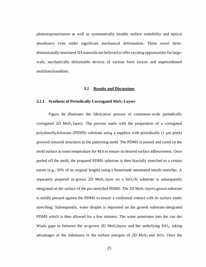
Figure 9: (a) Optical microscopy images of periodically corrugated 2D MoS2 layers on
PDMS over an area of ∼2 cm2. (b) Image of the same sample in sunlight showing
holographic reflection from the 2D MoS2 layers. (c) Side-view SEM image showing the
periodically corrugated structure of 2D MoS2 layers on PDMS. (d) Top-view AFM
topography image of the same sample. (e) 3D projected AFM topography image of the
same sample revealing the alternating appearance of hills and valleys with a periodicity of
1 μm. (f) AFM adhesion map profile corresponding to (d) and (e). (g) AFM height profile
(blue) and Young’s modulus mapping (red) of the same sample, revealing that the hill
regions are highly strained. Adapted with permission from reference [80] ..................... 29

xv
Figure 10: Periodically corrugated 2D MoS2 layers on PDMS in their (a) pristine and (b)
stretched states along with the corresponding schematic illustrations. (c, d) Two-
terminal I–V characteristics with increasing stretching for (c) periodically corrugated and
(d) plain 2D MoS2 layers without corrugation. (e) Comparison of ΔR/R
0 for periodically
corrugated vs plain 2D MoS2 layers. Adapted with permission from reference [80] ....... 32
Figure 11: (a) Optical absorbance spectra of periodically corrugated 2D MoS2 layers on
PDMS under varying stretch levels. A and B excitonic peaks are denoted. (b) Variation of
A excitonic peak energy under varying stretch levels. (c) Dynamic and reversible
photocurrent generation from 2D MoS2 layers on PDMS in a corrugated state. (d) Variation
of on/off photocurrent under varying stretch levels. Adapted with permission from
reference [80] .................................................................................................................... 34
Figure 12: Variation of WCA values for periodically corrugated 2D MoS2 layers under
varying stretch levels. (b, c) WCA measurements of PFOTES-treated periodically
corrugated 2D MoS2 layers at (b) 0% and (c) 50% tensile stretch. Adapted with permission
from reference [80] ........................................................................................................... 35
Figure 13: Schematic of the fabrication processes for kirigami-patterned, vertically aligned
2D PtSe2 layers on a flexible PI substrate. Adapted with permission from reference [96]
........................................................................................................................................... 39
Figure 14: (a) Camera images showing a bare PI (left) and an as-grown 2D PtSe2 layers-
on-PI substrate prepared by the CVD selenization of 8 nm Pt (right). (b and c) XPS
characterization of (b) Pt 4f and (c) Se 3d core levels obtained from 2D PtSe2 layers on PI
substrates. (d) EDS mapping images obtained from the corresponding 2D PtSe2 layers. (e)

xvi
HRTEM image of the corresponding sample showing vertically aligned 2D PtSe2 layers
along with their schematic illustration (inset). (f) STEM image showing the edges of
vertically aligned 2D PtSe2 layers with an interlayer spacing of ∼0.54 nm, corresponding
to the schematic illustration in the inset. Adapted with permission from reference [96] . 41
Figure 15: (a) Variation of current in an optimized 2D PtSe2/PI kirigami up to 2000% strain.
The inset illustrates the corresponding kirigami design with a = 17.2 mm, b = 0.4 mm,
and c = 0.375 mm. (b) Two-terminal I–V transport characterictics of the same kirigami
compared at various strain levels. (c) Electrical failure obtained from another kirigami
beyond ∼2300% strain. (d) Cyclic test to show the variation in current with a large number
of repeated stretchings measured at 3 V. (e) Camera images of the kirigami corresponding
to (a) and (b) upon manual stretching up to 2000% strain. (f) Schematic of an LED
continuity circuit using a 2D PtSe2/PI kirigami as a stretchable conductor. (g)
Demonstration of lighting up an LED by a 2D PtSe2/PI kirigami stretched to 0 and 1500%.
Adapted with permission from reference [96] .................................................................. 44
Figure 16: (a) Camera image of CNT/2D PtSe2 layer-based kirigami. (b) Variation of
current observed with CNT/2D PtSe2 layer-based kirigami with ON/OFF illumination
cycles. (c) Energy band diagram illustrating photocurrent generation at the CNT/2D
PtSe2 Schottky junction. (d) Plots of current vs strain obtained with the kirigami in (a)
with/without illumination for up to 75% strain. (e) Plots of current vs strain obtained with
the CNT/2D PtSe2kirigami of optimized geometrical parameters stretched up to 1500%
strain with/without illumination. (f) Demonstration of the reversibility in photocurrent

xvii
generation upon an application/release of tensile stretch. Adapted with permission from
reference [96] .................................................................................................................... 46
Figure 17: (a) Schematics showing the defining geometrical parameters for the
unoptimized (left) vs optimized (right) kirigami patterns. (b, c) FEM simulations showing
the strain distribution within the kirigami patterns of (b) unoptimized and (c) optimized
parameters. (d) Graphical comparison of maximum in-plane principal strain vs stretch for
the unoptimized (blue plot) vs optimized (red plot) kirigami patterns. The inset compares
the simulated vs experimentally demonstrated images of kirigami patterns while their
failure point is approximated to be ∼0.1 times the maximum in-plane principal strain. (e–
g) Plots of maximum in-plane principal strain vs stretch with varying geometrical
parameters of (e) a, (f) b, and (g) c. Adapted with permission from reference [96] ........ 49
Figure 18: (a) HRTEM image of horizontally aligned thin 2D PtSe2 layers. (b) I
ds–
Vds
transfer characteristics from a back-gated FET based on horizontally aligned thin 2D
PtSe2 layers configured on a SiO
2/Si wafer. (c) Schematic illustration of an electrolyte
gating of a 2D PtSe2/PI FET. (d) I
ds–V
g and (e) I
ds–V
ds transfer characteristics from a 2D
PtSe2/PI FET. The scale bar in the inset of (d) is 1 mm. (f) I
ds–V
g transfer characteristics
from a 2D PtSe2/PI kirigami FET. (g) Camera images of the kirigami FETs corresponding
to (f). Adapted with permission from reference [96] ........................................................ 52
Figure 19: (a) Photos of 2D PtTe2 layers-grown flexible PI substrates prepared with Pt
films of various thicknesses. (b) The maximum temperature of 2D PtTe2/PI samples
prepared with various Pt thickness achieved at biases of 3, 5, and 7 V. (c) Time-dependent
temperature fall/rise of the same samples in (b) obtained at 5 V. (d) Determination of the
xviii
heating/cooling rate corresponding to (c). (e) Temperature variation obtained from a 2D
PtTe2-6nm/PI sample during the cyclic heating/cooling of 50 times at 4 V. (f)
Representative IR images of the sample in (e) at three different cycle numbers. (g)
Demonstration of the solar energy-driven operation of 2D PtTe2/PI heaters. (h)
Temperature variations achieved with 2D PtTe2/PI heaters of various thickness driven by
solar energy. Adapted with permission from reference [114] .......................................... 58
Figure 20: (a) Schematic illustrations for the fabrication process of Kirigami-patterned 2D
PtTe2 layers-based stretchable heater. The insets show representative images of a
fabricated heater before/after stretching. (b) Sketch of the Kirigami pattern adopted in this
experiment defining the geometrical parameters of a, b, and c. (c) IR images of a 2D
PtTe2/PI Kirigami heater (insets) and the corresponding plots of Tmax vs. strain rate for
various applied voltages. (d) Variations of Tmax and R/R0 obtained from the same sample in
(c) during the cyclic stretch of 1,000 times with 70% of strain. Adapted with permission
from reference [114] ......................................................................................................... 62
Figure 21: Schematic overview of Kapton-based Pt-TMD tattoo design and fabrication
flow. (a) Evaporation of thin Pt on top of the Kapton film, followed by TAC conversion
into Pt-TMD. (b) Schematic of the TAC CVD process. (c) Post-CVD growth, the Pt-
TMD/Kapton sample is fixed on top of a TRT. (d) Mechanical patterning process of the
Pt-TMDs grown on Kapton film. (e) Schematics of the final PtSe2 and PtTe2 tattoos
supported by Kapton. Adapted with permission from reference [120] ............................ 64
Figure 22: Wearable electrophysiological recordings with Pt-TMDs. (a) Schematic of the
electrode placement for the ECG measurement. (b) Five-second-long ECG timetrace from
PtTe2 tattoos and Ag/AgCl gel electrodes. (c) Average ECG signal shapes, amplitudes, and

xix
average SNRs for PtTe2 tattoo and Ag/AgCl gel electrode. (d) Schematic of electrode
placement and EMG recordings from a human’s bicep (top) and forearm (bottom) muscle
contractions recorded via the Ag/Ag gel electrodes and PtTe2 tattoos simultaneously. The
horizontal bars on the top and bottom mark the events and durations of the bicep curls and
forearm contractions correspondingly. (e) Electrode placement for EEG measurements
(left) and resulting spectrogram (right) from one of the PtTe2 tattoos placed on the Fp1 and
Fp2 locations on the subject’s forehead. Adapted with permission from reference [120] 68
Figure 23: (a) Schematic of the electrode placement for the EOG experiments performed
with PtTe2 tattoos. (b) EOG signals corresponding to the differential channel recording
left–right eye movements (violet here and after). (c) EOG signals corresponding to the
differential channel recording up–down eye movements (green here and after). (d) EOG
recordings from both channels when the subject is gazing up, right, right, left, down, down,
and left consecutively with 5 s dwell time. (e) EOG recordings from both channels when
the subject is looking counterclockwise with four distinct stops: at “12”, “9”, “6”, and “3”
o’clock. Straight and angular arrows in (d,e) correspondingly show the direction of sight.
Adapted with permission from reference [120] ................................................................ 69
Figure 24: Schematic of the fabrication process for the PDMS/PtTe2/PI soft bimorph
actuator. (b) Digital image showing the U-shaped PDMS/PtTe2/PI bimorph actuator.
Schematic showing the (c) top and (d) side view profile of the and schematic showing the
top view (middle) and side view profile (bottom) of the PDMS/PtTe2/PI bimorph actuator
dimensions. ....................................................................................................................... 74
Figure 25: Characterization of the bending performance of the actuator (a,b) Optical images
of the PtTe2/PI actuator in a suspended geometry at different time moments when

xx
(a)Voltage is turned on and (b) Voltage is turned off (c) Maximum curvature achieved at
different voltages (d) The resulting actuation curvature over repetitive cycles at applied
voltage of 20V (e) Cyclic graph of maximum curvature of the actuator up to 50 cycles
with applied voltage of 20V. ............................................................................................. 77
Figure 26: Characterization of the bending performance of the actuator (a,b) Optical images
of the PtTe2/PI actuator in a suspended geometry at different time moments when
(a)Voltage is turned on and (b) Voltage is turned off (c) Maximum curvature achieved at
different voltages (d) The resulting actuation curvature over repetitive cycles at applied
voltage of 20V (e) Cyclic graph of maximum curvature of the actuator up to 50 cycles
with applied voltage of 20V. ............................................................................................. 79
Figure 27: Two PtTe2 soft actuators were integrated as bi-finger gripper and images were
taken showing its application for pick-and place operations. (a) Top-view schematic
illustration showing electrical connection of the two actuators. (b,c) A “bi-finger”
mechanical gripper with (b) voltage turned off and (c) 20V turned on. Images were taken
showing its application for pick-and place operations; (d,e) approaching and gripping, (f,g)
lifting and transferring, (h,i) releasing. ............................................................................. 81
Figure 28: (a) Digital images of 2D PtTe2 layers/WG samples prepared by the tellurization
of 0 nm, 0.75 nm, 1.5 nm, and 3 nm thick Pt films (top to bottom). (b, c) XPS
characterization of (b) Pt 4f and (c) Se 3d core levels obtained from 2D PtTe2 layers/WG.
(d) Optical transmittance of 2D PtTe2 layers/WG in the ultraviolet–visible wavelength
region. (e) Sheet resistance of Pt films before and after tellurization as a function of their

xxi
thickness. (f) Sheet resistance and optical transmittance of 2D PtTe2 layers prepared with
Pt films of various thicknesses. Adapted with permission from reference [71] ............... 85
Figure 29: (a, b) IR images of 2D PtTe2 layers/WG samples prepared with Pt films of (a)
0.5 nm and (b) 1 nm thickness. (c) Voltage-dependent temperature profiles of 2D
PtTe2 layers/WG samples prepared with Pt films of various thicknesses. (d) Optical
transmittance of 2D PtTe2 layers/mica samples in the UV-vis wavelength region. The inset
shows digital images of a mica substrate before (left) and after (right) the growth of 2D
PtTe2 layers by tellurizing 1 nm Pt film. (e) Voltage-dependent IR images of the 2D
PtTe2layers/mica sample corresponding to (d). (f) Voltage-dependent temperature profile
obtained from the sample in the inset. (g) Temperature profile obtained from the cyclic
application of ON/OFF voltages 50 times. Adapted with permission from reference [71]
........................................................................................................................................... 87
Figure 30: (a) Schematic diagrams showing the fabrication and operation of the 2D
PtTe2 layers/WG-based thermochromic displays. (b) Digital images demonstrating the
voltage-driven reversible operation of a thermochromic display at biases of 0 V and 5 V.
(c) IR images of the sample corresponding to (b). (d) Cyclic performance of the
thermochromic displays at fixed input biases of 5 V and 10 V. Adapted with permission
from reference [71] ........................................................................................................... 90
Figure 31: (a) Water contact angles of a WG substrate in its pristine state, after the
deposition of 1.5 nm Pt film and growth of 2D PtTe2 layers (left to right). (b) Image of a
WG substrate under compressive strain retaining a bending radius of ∼1.3 cm. (c)
Demonstration of electrically driven defogging in a mechanically-flexible 2D

xxii
PtTe2 layer/WG sample. (d) Performance comparison of various state-of-the-art
nanomaterials developed for defogging windows. Adapted with permission from reference
[71] .................................................................................................................................... 92

xxiii
LIST OF ACRONYMS (or) ABBREVIATIONS
0D One-Dimensional
2D Two-Dimensional
3D Three-Dimensional
2D TMD Two-Dimensional Transition Metal Dichalcogenide
CTE Coefficient of Thermal Expansion
CVD Chemical Vapor Deposition
EOG Electrooculography
EEG Electroencephalogram
ECG Electrocardiogram
EMG Electromyogram
FEM Finite Element Method
HRTEM High Resolution Transmission Electron Microscopy
PDMS Polydimethylsiloxane
PMMA Poly (methyl methacrylate)
SEM Scanning Electron Microscopy
TAC Thermal Assisted Conversion
TEM Transmission Electron Microscopy
XPS X-ray Photoelectron Spectroscopy
1
CHAPTER 1 INTRODUCTION
1.1 Emerging Reconfigurable Electronics
We live in an era of rapid advancement in electronics, with increasing demand for
lighter, faster, flexible as well as wearable devices to accommodate the evolving needs of
present and future developments across various fields and applications including smart
displays, Internet-of- Things (IoT), wearable devices and soft robotics [1-4]. More recently,
the concept of mechanically reconfigurable electronics has been used to describe a type of
emerging technology that goes beyond flexible and bendable devices deformable in the
out-of-plane direction only. Rather, it comprises of electro-mechanical properties that are
challenging to realize in conventional approaches; for example, devices that can change
their geometry and multiple desired physical properties under the application of external
mechanical stimuli and fully recover in a self-adaptable manner, or those that are extremely
conformal or stretchable in an in-plane manner. Such mechanical reconfigurability requires
that the electronic devices conform to repeated deformations of stretching, compression,
rolling and twisting, thus imposing significant challenge to traditional electronic
technology based on rigid and brittle thin films like silicon. For instance, wearable devices
for personal healthcare ideally require large degree of conformability and reversibility as
they undergo multi-directional deformation to accommodate the locomotion of the human
skin or organs. Such transition from conventional rigid and bulky electronics to
mechanically reconfigurable electronics devices is not direct, requiring either active
materials that are intrinsically mechanically reconfigurable or novel geometric designs of
individual components in an integrated manner. Approaches based on the design of

2
geometric design of individual components have been realized through fabricating wavy
interconnects between stiff areas or loading conductive nanomaterials in soft polymers.
Other approaches for mechanically reconfigurable devices have relied on the innovation of
both organic and inorganic materials. For example, there have been reports of organic
polymers with inherent flexibility and stretchability enabling their applicability for
mechanically reconfigurable and structurally curved devices[5-7]. However, the complex
manufacturing processes as well as chemical and thermal instability outweighs the
advantages of high mechanical deformability[8, 9]. In contrast, inorganic materials present
high thermal and chemical stability, as well as excellent electrical performance and
mechanical robustness; it however remains a challenge to increase their intrinsic
deformability [10, 11]. To realize the true technological potential of mechanically
reconfigurable electronics, there is the need for combined innovation in the area of active
materials with intrinsic electro-mechanical properties and creative manufacturing and
patterning techniques.
1.2 2D Materials
Two-dimensional (2D) materials have garnered substantial attention and have been
identified as one of the top emerging technologies to drive the fourth industrial revolution
owing to their exceptional properties and potential applications for futuristic electronics
including flexible, transparent, ultra-thin and wearable electronics.[12] There has been
increased intensive research on ultrathin 2D nanomaterials in the fields of material science,
chemistry, condensed matter physics and nanotechnology since the successful isolation of
graphene in 2004, which showed a variation of properties from its 3D counterpart,

3
graphite.[13] These materials offer a new platform with unique opportunities through novel
electronic, physical and chemical properties owing to electron confinement in two
dimensions. Till date there is a large portfolio of 2D materials with exotic electronic,
magnetic, mechanical, vibrational and topological properties making them suitable for
applications in electronics, spintronics, supercapacitors, sensing and emerging
neuromorphic computing.[14] In particular, the intriguing mechanical and electrical
properties of atomically-thin 2D materials have made them a focus of nanoelectronics
research. Due to their ultrathin nature, they have high mechanical flexibility with the
absence of dangling bonds making them suitable for mechanically reconfigurable
electronics.[15]
1.3 Graphene
Graphite is a naturally occurring allotrope of carbon, well known for its flaky and
easily cleavable nature and wide range of uses, ranging from dry lubricant to writing tools
throughout history. However, its two-dimensional counterpart was only speculated in
theory and was long believed to be unable to exist independently.[16] A major
breakthrough occurred in 2004, when K.S Novoselov and A.K. Geim successfully isolated
graphene, an atom thick layer of graphite, through mechanical exfoliation . [13] Graphene
has since then been the most studied 2D material, partly because it was the first to be
isolated but majorly because of its astounding properties including optical transparency,
high Young’s modulus, high room-temperature carrier mobility, quantum Hall effect, and
excellent thermal and electrical conductivities. [17-20]
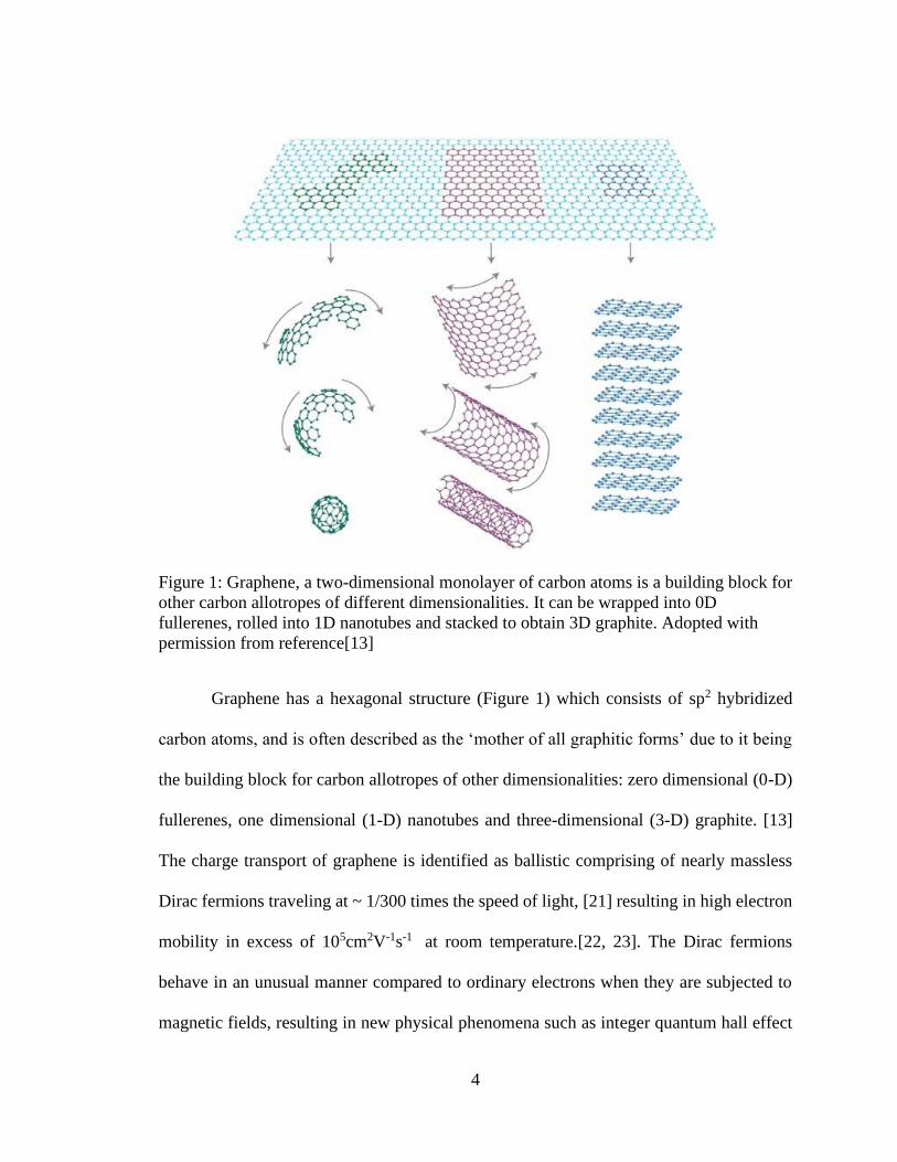
4
Figure 1: Graphene, a two-dimensional monolayer of carbon atoms is a building block for
other carbon allotropes of different dimensionalities. It can be wrapped into 0D
fullerenes, rolled into 1D nanotubes and stacked to obtain 3D graphite. Adopted with
permission from reference[13]
Graphene has a hexagonal structure (Figure 1) which consists of sp2 hybridized
carbon atoms, and is often described as the ‘mother of all graphitic forms’ due to it being
the building block for carbon allotropes of other dimensionalities: zero dimensional (0-D)
fullerenes, one dimensional (1-D) nanotubes and three-dimensional (3-D) graphite. [13]
The charge transport of graphene is identified as ballistic comprising of nearly massless
Dirac fermions traveling at ~ 1/300 times the speed of light, [21] resulting in high electron
mobility in excess of 105cm2V-1s-1 at room temperature.[22, 23]. The Dirac fermions
behave in an unusual manner compared to ordinary electrons when they are subjected to
magnetic fields, resulting in new physical phenomena such as integer quantum hall effect
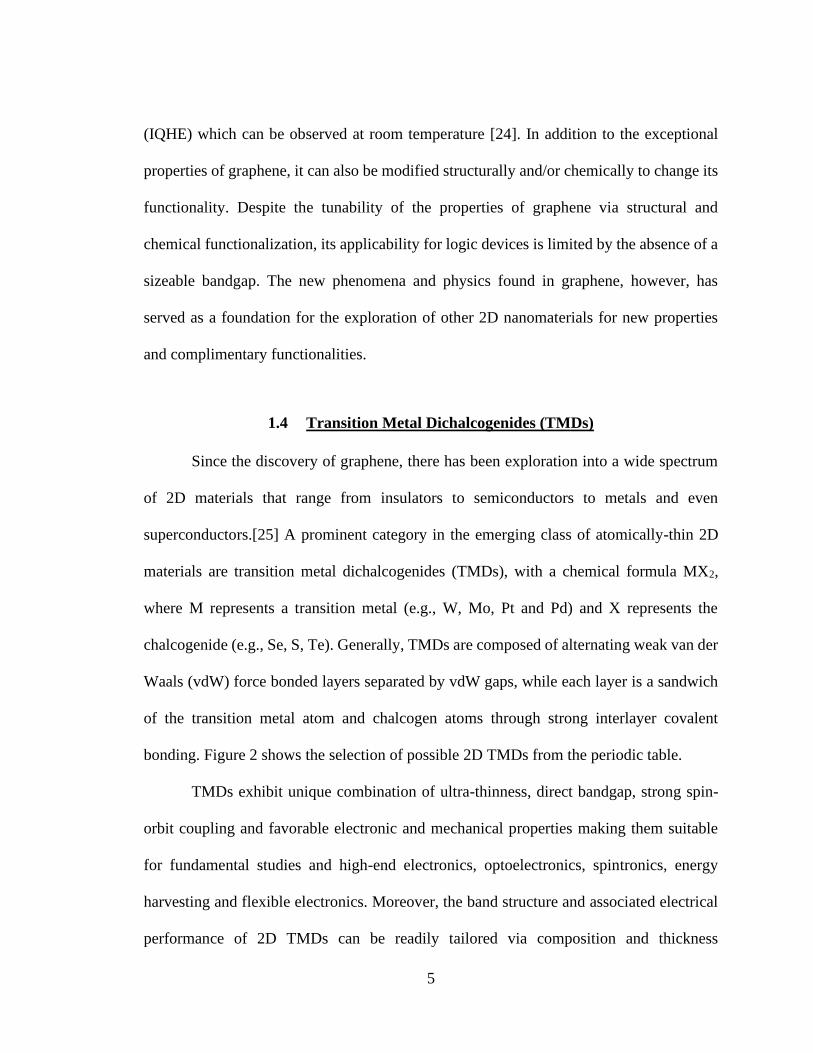
5
(IQHE) which can be observed at room temperature [24]. In addition to the exceptional
properties of graphene, it can also be modified structurally and/or chemically to change its
functionality. Despite the tunability of the properties of graphene via structural and
chemical functionalization, its applicability for logic devices is limited by the absence of a
sizeable bandgap. The new phenomena and physics found in graphene, however, has
served as a foundation for the exploration of other 2D nanomaterials for new properties
and complimentary functionalities.
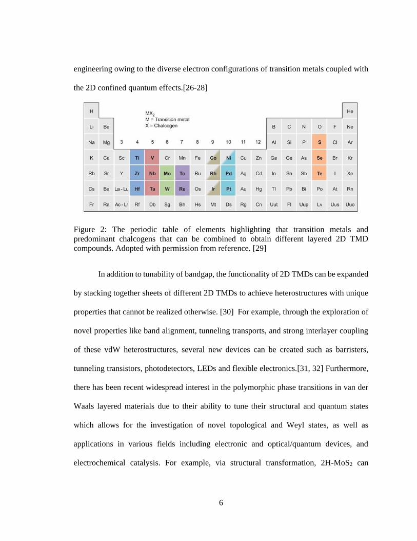
1.4 Transition Metal Dichalcogenides (TMDs)
Since the discovery of graphene, there has been exploration into a wide spectrum
of 2D materials that range from insulators to semiconductors to metals and even
superconductors.[25] A prominent category in the emerging class of atomically-thin 2D
materials are transition metal dichalcogenides (TMDs), with a chemical formula MX2,
where M represents a transition metal (e.g., W, Mo, Pt and Pd) and X represents the
chalcogenide (e.g., Se, S, Te). Generally, TMDs are composed of alternating weak van der
Waals (vdW) force bonded layers separated by vdW gaps, while each layer is a sandwich
of the transition metal atom and chalcogen atoms through strong interlayer covalent
bonding. Figure 2 shows the selection of possible 2D TMDs from the periodic table.
TMDs exhibit unique combination of ultra-thinness, direct bandgap, strong spin-
orbit coupling and favorable electronic and mechanical properties making them suitable
for fundamental studies and high-end electronics, optoelectronics, spintronics, energy
harvesting and flexible electronics. Moreover, the band structure and associated electrical
performance of 2D TMDs can be readily tailored via composition and thickness
6
engineering owing to the diverse electron configurations of transition metals coupled with
the 2D confined quantum effects.[26-28]
Figure 2: The periodic table of elements highlighting that transition metals and
predominant chalcogens that can be combined to obtain different layered 2D TMD
compounds. Adopted with permission from reference. [29]
In addition to tunability of bandgap, the functionality of 2D TMDs can be expanded
by stacking together sheets of different 2D TMDs to achieve heterostructures with unique
properties that cannot be realized otherwise. [30] For example, through the exploration of
novel properties like band alignment, tunneling transports, and strong interlayer coupling
of these vdW heterostructures, several new devices can be created such as barristers,
tunneling transistors, photodetectors, LEDs and flexible electronics.[31, 32] Furthermore,
there has been recent widespread interest in the polymorphic phase transitions in van der
Waals layered materials due to their ability to tune their structural and quantum states
which allows for the investigation of novel topological and Weyl states, as well as
applications in various fields including electronic and optical/quantum devices, and
electrochemical catalysis. For example, via structural transformation, 2H-MoS2 can

7
achieve a metallic 1T phase which can be employed as contact in homojunction devices to
reduce the Schottky barrier at the metal-semiconductor interface.[33]
Majority of the exploration in the layered 2D material landscape beyond graphene
has been centered around group-6 TMDs – MoS2, MoSe2, WS2, WSe2 with semiconducting
carrier transport accompanying 2D layer-dependent bandgap energy change. More
recently, group-10 TMDs (based on metals of Pd, Ni and Pt), previously been largely
underexplored, have triggered studies owing to their improved electrical and optoelectrical
properties. Group-10 TMDs such as PtSe2, PtTe2 have demonstrated wide-tunable indirect
bandgap of 0.25 eV – 1.6 eV, and ~ 0 eV -1.2 eV, respectively, from bulk to monolayer
[34, 35], while monolayer PtS2 has an indirect bandgap of 1.68 eV [36]. Recent reports on
PtTe2 an emerging type-II Dirac semimetal have also projected intriguing quantum
phenomena such as anisotropic magnetism and topological transition with a transition to
semiconductor with a bandgap of ~0.4 eV when it is in monolayer form. [36] Additionally,
Pt-based TMDs are projected to offer process capability advantages over group-6 TMDs
owing to melting temperature of elemental Pt being less (~2/3) than that of Mo (or W), and
hence allowing growth to occur at much lower temperatures. [37]
1.5 Motivation
1.5.1 Why 2D TMDs for Mechanically Reconfigurable Electronics
The advent of few-atom thick 2D layers has gained extensive research attention for
mechanically reconfigurable electronics devices owing to their intrinsic exceptional
electrical and mechanical properties [38, 39]. In contrast to zero bandgap graphene, 2D

8
TMDs offers more opportunities for electronics devices due to their diverse range of
properties including semiconducting, semi-metallic, or even superconducting properties.
Owing to the diverse electronic configurations and 2D confined quantum effects, the band
structures and electrical properties of 2D TMDs can be tailored through composition and
thickness engineering. Furthermore, their extreme thinness – down to ultimate physical
dimension of a single atom thickness, offers them ultra-high in-plane low bending stiffness
and high in-plane Young’s modulus, giving them the desired bending and stretching
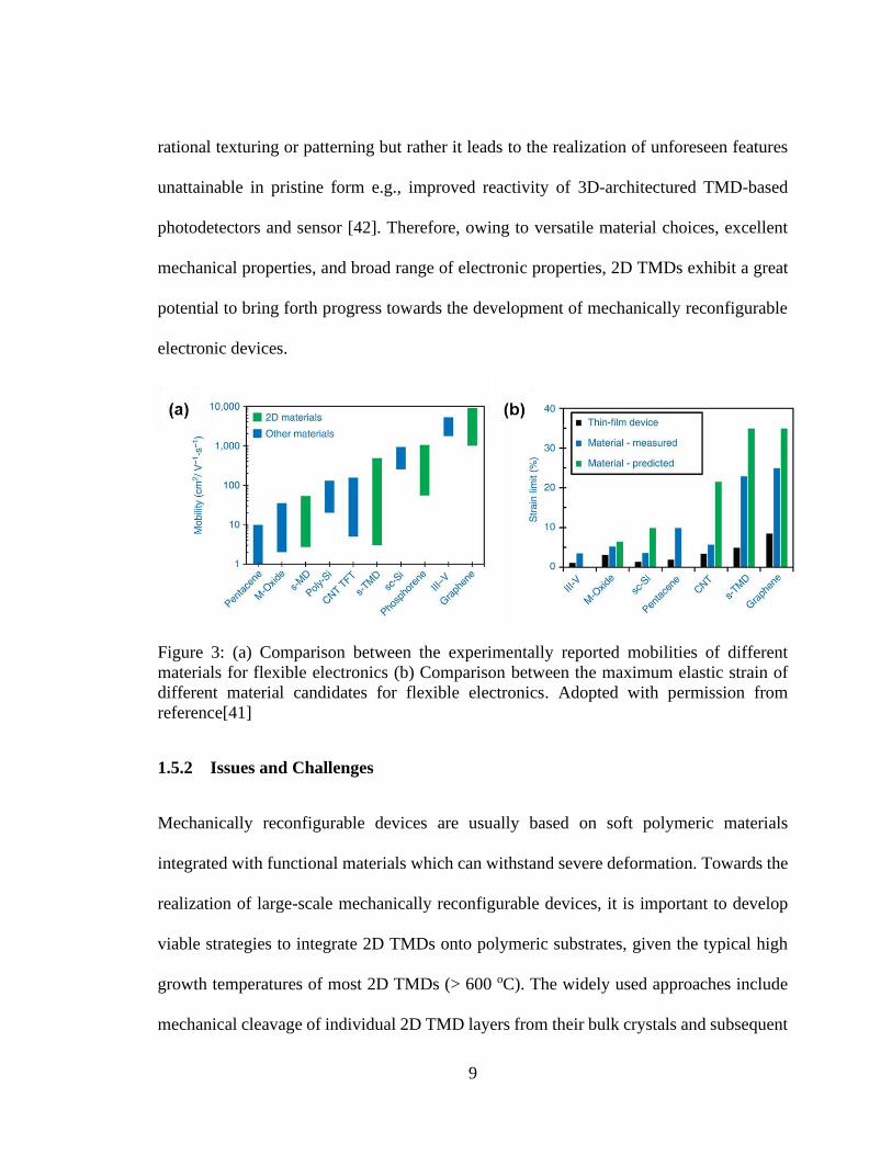
capabilities for mechanically reconfigurable devices. For example, a recent report states
that monolayer MoS2 possesses a breaking strength of 22 GPa, Young’s modulus of 270
GPa and a maximum durable strain of 11% [40]. Additionally, owing to the weak vdW
bonding nature of 2D TMD layers, they can be integrated onto arbitrary substrates without
lattice constraint as opposed to conventional thin film growths. Figure 3a shows the
comparison between the reported charge mobilities of candidate materials for Field Effect
Transistors (FETs) indicating that 2D TMDs with large bandgaps (for example, WSe2,
MoS2) offer experimental mobilities approaching single crystalline silicon thin film
transistors [41]. Similarly, Figure 3b compares the maximum elastic strain limits of
different materials indicating that 2D TMDs offer higher theoretical and measured strain
limits compared to conventional bulk 3D materials. In addition to the superior electrical
and mechanical advantages that 2D TMDs have compared to graphene and other
conventional materials, it is noteworthy to that their electrical and mechanical properties
are correlated with morphological transformation and physical deformation. For instance,
changes in the electronica band structure can be induced through structural instabilities
such as wrinkles or crumples. Additionally, their original properties are not impaired by
9
rational texturing or patterning but rather it leads to the realization of unforeseen features
unattainable in pristine form e.g., improved reactivity of 3D-architectured TMD-based
photodetectors and sensor [42]. Therefore, owing to versatile material choices, excellent
mechanical properties, and broad range of electronic properties, 2D TMDs exhibit a great
potential to bring forth progress towards the development of mechanically reconfigurable
electronic devices.
Figure 3: (a) Comparison between the experimentally reported mobilities of different
materials for flexible electronics (b) Comparison between the maximum elastic strain of
different material candidates for flexible electronics. Adopted with permission from
reference[41]
1.5.2 Issues and Challenges
Mechanically reconfigurable devices are usually based on soft polymeric materials
integrated with functional materials which can withstand severe deformation. Towards the
realization of large-scale mechanically reconfigurable devices, it is important to develop
viable strategies to integrate 2D TMDs onto polymeric substrates, given the typical high
growth temperatures of most 2D TMDs (> 600 oC). The widely used approaches include
mechanical cleavage of individual 2D TMD layers from their bulk crystals and subsequent

10
integration onto target substrates [43]. However, this method suffers from several
drawbacks including limited controllability over spatial uniformity (e.g., thickness) of the
2D layers [44]. Similarly, there have been strategies based on adhesive polymers such as
PMMA to transfer 2D TMD layers in a more controlled manner [45, 46]. However, these
methods typically require the chemical etching of growth substrate layer(s) and subsequent
dissolution of the carrier polymer. These methods have been widely used but also come
with several drawbacks that remain to be overcome e.g., bubble generation during the
etching phase and incomplete removal of polymer residue after the 2D layer lift off.
Alternatively, there have been explorations into the use of thermal release tapes (TRTs) to
detach 2D TMD layers from their growth substrate and the subsequent removal of the TRT
after integration through mild heat offering[47, 48]. Although, TRT-based transfer
approaches offer the advantage of cleaner morphology compared to PMMA, the efficiency
of transfer is strongly dependent on the adhesion properties of the 2D TMDs with the
substrate surfaces. To overcome the limitations of polymer-based transfer approaches, new
non-polymer-based techniques have been developed such as a layer-resolved splitting
(LRS) technique based on the interfacial toughness and strain difference between grown
2D-layers and growth substrate[49]. However, this method involves complicated
fabrication with non-typical synthesis and imposes scalability limitations.
Furthermore, despite the projected merits of 2D TMDs for mechanical
reconfigurability, the realization of large-scale 2D TMDs in a tailored structure which
allows for extreme property advantages under such severe mechanical deformation, has
remained challenging. For example, although theoretical estimates indicate that 2D MoS2
layers can present a high in-plane strain limit of ~ 30% [40, 50], the stretchability of
11
chemically grown MoS2 layers is much limited; experimental examples show significant
electrical failure at a tensile strain of ~ 5% [51], leading to severe limitations in
applicability requiring larger mechanical tolerance. In addition to the preservation of
intrinsic material properties, it is desirable to modulate them in a controllable manner to
further broaden the versatility of the material. A variety of approaches have been explored
to convert intrinsically brittle electronic materials to stress-resilient forms by rationally
engineering their physical configurations and dimensions [42, 52, 53]. Substantive efforts
on the 3D structuring of 2D TMD layers been devoted with a variety of
motivations[54], including “crumpled” 2D MoS2 layers integrated on
mechanically/thermally responsive substrates[55, 56]. Three-dimensionally oriented 2D
layers have also been achieved during their natural growth stages dictated by material
growth parameters [57, 58]. The integration of pre-grown 2D TMD (MoS2) layers on
flexible substrates has previously been attempted to achieve three-dimensionally structured
2D layers via substrate engineering [59, 60] wherein the integration typically remains on
small areas (<cm2). Moreover, in such cases, the integrated 3D MoS2 layers suffer from a
large degree of random layer orientation with uncontrolled morphologies. Additionally,
engineering patterning techniques such as Origami and Kirigami [61, 62] are projected to
have merits and induce tunable multifunctionalities. despite the projected advantages,
converting 2D TMDs into Kirigami forms has been rarely attempted, leaving their
anticipated mechanoelectrical superiority largely unexplored. While some proof-of-
concept demonstrations have been predicted by theory[63, 64], the experimental realization
of “stand-alone” 2D TMD-based Kirigami patterning has been unavailable. This limitation
is attributed to the technical difficulty associated with reliably handling extremely thin 2D
12
layers in a free-standing form. As a result, limited success has been demonstrated with the
graphene Kirigami of a very small dimension (≲100 μm2) realized by highly sophisticated
lithographic fabrication processes[65].
To this end, the aim of this thesis is to make advancements in coping with these
challenges and advance the realization of mechanically reconfigurable devices based on
2D TMDs.
1.6 Objectives
The main objectives of this thesis are as follows:
1. To study and develop scalable techniques to grow high-quality wafer-scale (i.e., >
cm2) 2D TMDs on different substrates (rigid and polymeric)
2. To develop scalable and green technique to transfer as grown 2D TMDs from their
growth substrates to arbitrary target substrates while retaining their structural
integrity.
3. To utilize creative structural engineering techniques including corrugated
patterning and Kirigami to obtain 3D-architected 2D TMDs that are mechanically
reconfigurable, with improved and tunable functionalities.
4. To realize large-scale mechanically reconfigurable electronics devices based on 2D
TMDs including stretchable semiconductors and conductors, stretchable
transistors, smart wearable heaters and tattoo sensors, smart windows, smart
display and soft actuators.
13
1.7 Dissertation Overview
Chapter two starts with the methods and techniques used to obtain large-area high
quality 2D TMD as well as our developed novel green technique to transfer the materials
onto arbitrary substrates.
After the development of these growth and transfer techniques, chapter three
presents the development of a multifunctional periodically corrugated MoS2 using the
above-described growth methods and water transfer. The process of obtaining the
corrugated MoS2 layers and the structural, electrical, mechanical, and optical
characterizations are presented in this chapter.
Chapter four presents the 3D architecting of Pt-based 2D TMDs using Kirigami
patterning technique. In this chapter, the experimental procedure for obtaining the Kirigami
pattern is presented, as well as characterizations of the performance of the Kirigami
patterned device and its applicability. We also show the applicability of the Kirigami
patterned materials as stretchable conductors and transistors.
In chapter five, we present the application of the Kirigami patterning technique
described in chapter four, and similar serpentine patterning methods to develop wearable
devices based on PtTe2. We explore the properties of PtTe2 that makes it applicable for
wearable devices and explore its application for wearable heaters and tattoos sensors. We
show the methods to obtain these devices and the characterizations.
In chapter six, we explore the application of the exceptional electrothermal
properties of PtTe2 described in chapter five for soft robotics. We employed PtTe2 layers
in a biomorph configuration and realized actuation motion which we characterized in
14
detail. We also show the application of the developed biomorph actuator as a bi-finger
gripper mimicking humanoid motion for pick-and-place operations.
In chapter seven, we present smart electrothermal windows based on PtTe2.
Synthetic method to obtain the smart windows are presented as well as electrothermal,
electrical, and mechanical performance of the PtTe2 layers. Proof-of-concept
demonstrations of the PtTe2 smart windows for thermochromic display and self-defogging
are also presented.
Chapter eight concludes the dissertation and projects the possible future directions
that need to be explored to realize the full technological potential of 2D TMDs.
15
CHAPTER 2 SCALABLE GROWTH AND INTEGRATION OF
2D TMDs
The contents of this chapter have been published in:
Kim, J. H., T.-J. Ko, E. Okogbue, S. S. Han, M. S. Shawkat, M. G. Kaium, K. H. Oh, H.-S.
Chung and Y. Jung (2019). "Centimeter-scale Green Integration of Layer-by-Layer 2D
TMD vdW Heterostructures on Arbitrary Substrates by Water-Assisted Layer Transfer."
Scientific Reports 9(1): 1641.
Emmanuel Okogbue, Tae-Jun Ko, Sang Sub Han, Mashiyat Sumaiya Shawkat, Mengjing
Wang, Hee-Suk Chung, Kyu Hwan Oh, Yeonwoong Jung (2020) “Wafer-Scale 2D Ptte2
Layers for High-Efficiency Mechanically Flexible Electro-Thermal Smart Window
Applications” Nanoscale, 12, 10647-10655
2.1 Introduction
A few critical prerequisites exist in order to realize the advantages inherent to 2D TMDs
toward their exploration for novel technologies; (1) There is the need to develop scalable
growth methods to obtain high quality and wafer-scale 2D TMDs with controlled layer
chemistries/morphologies (2) It is demanded to develop viable strategies to transfer 2D
TMD layers from original growth substrates and integrate them on secondary substrates of
targeted functionalities, e.g., mechanically flexible substrates. (3) The intrinsic mechanical
and electrical properties of the transferred 2D layers should not be compromised
throughout their integration process and should be uniformly preserved on a wafer scale.
(4) The layer integration process should be generalized to 2D TMDs and substrates of
16
diverse materials without being limited to specific kinds for technological versatility.
Presently, the most commonly employed approach for the transfer and integration of 2D
TMD layers relies on the chemical etching of underlying growth substrates involving
protection polymers (e.g., polymethyl-methacrylate (PMMA)) and subsequent chemical
lift-off [66, 67]. However, such strategies tend to result in the fragmentation of individual
2D layers as they employ solution-based chemicals to etch away both the protection layer
and growth substrates (e.g., silicon dioxide (SiO2) or sapphire wafer)[67]. Accordingly,
they impose scalability limitation in terms of heterogeneously stacking up 2D layers of
multiple components in a controlled manner as well as being difficult to be applied to a
variety of unconventional substrates. Moreover, the intrinsic material properties of 2D
layers are often compromised and damaged by the employed chemicals though their
transfer and integration stages.
In this chapter, we report a generic and reliable strategy to achieve the layer-by-layer
integration of 2D TMDs of controlled morphology and component onto arbitrary substrates
over a large area. The newly developed 2D layer integration method is intrinsically “green”
as it employs water only without involving any other chemicals, thus is free of any
chemicals-associated material degradation. We demonstrate the layer-by-layer integration
of centimeter-scale (>2 cm2) uniform 2D TMDs and their heterostructures onto virtually
arbitrary substrates including, papers, woods, and plastics, which is difficult to achieve
with any conventional approaches. The integrated 2D TMD layers and their
heterostructures well preserve their original structural and compositional integrity

17
benefiting from the intrinsic cleanness of the water-assisted process, confirmed by
extensive spectroscopy and microscopy characterization.
2.1.1 Thermal Assisted Conversion
The growth of 2D TMD layers on various substrates is carried out using a two-step thermal
assisted conversion process. Electron beam deposition is used to deposition metal seed
layer of desired thickness on various substrates (e.g., silicon dioxide/silicon (SiO2/Si),
mica). The metal-deposited substrates are then loaded in the quartz tube in the CVD tube
furnace for thermal assisted conversion into 2D TMD layers. The CVD tube is connected
to pump to remove residual gases and the material growth is carried out at a base pressure
of 25 mTorr using Argon (Ar) gas. Figure 4 below shows a pictorial representation of our
table-top CVD setup used for routine material growth.
Figure 4: A picture of the CVD furnace used for routine growth of 2D TMDs.
Cold TrapFlow
meter
Gas valve
Pressure Readout
High temperature Furnace
Movable base

18
2.1.2 Low Temperature CVD growth of Pt-based TMDs
Emerging Pt-based 2D TMDs (PtTe2, PtSe2) are advantageous because they can be grown
at much lower temperatures (400 oC) compared to other 2D TMD counterparts such as
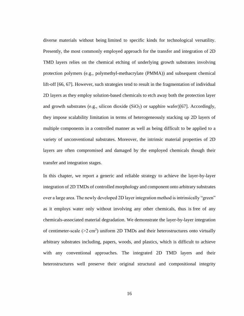
MoS2, MoSe2, WS2, requiring growth temperatures > 600 oC. Figure 5a presents a
schematic illustration of the growth of wafer-scale 2D PtTe2 layers on various substrates,
which is carried out in two-step procedures; Pt films of controlled thickness are deposited
on growth substrates (e.g., silicon dioxide/silicon (SiO2/Si), willow glass (WG), and mica)
followed by thermal tellurization at 400 °C, similar to our previous studies [57, 68]. The
Pt-deposited growth substrate and tellurium powder are placed in the mid- and up-stream
side of a CVD tube furnace, respectively. The tube is pumped down to a base pressure of
25 mTorr followed by Ar gas purging and is subsequently filled with Ar gas of 100 sccm
(standard cubic centimeter per minute). The temperature of the furnace center zone is
maintained at 400 °C for 50 min yielding the conversion of Pt to 2D PtTe2 layers. Figure
5b shows a representative image of wafer-scale 2D PtTe2 layers as-grown on a SiO2/Si
substrate. Figure 5c exhibits the Raman profile obtained from a sample of as-grown 2D
PtTe2 layers on a SiO2/Si substrate. Two characteristic peaks are observed at t ≃115
cm−1 and ≃159 cm−1, which correspond to the in-plane (Eg) and out-of-plane (A1g)
vibration modes of 1T-phased PtTe2, respectively. Figure 5d show the XPS profile specific
to the core energy levels of Pt and Te elements from a sample of the as-grown 2D PtTe2
layers/WG, respectively. The XPS profile in Figure 5d (left) exhibits the Pt-4f core level
peaks at 72.2 eV and 75.5 eV corresponding to 4f 7/2 and 4f 5/2, respectively, which well
agrees with previous studies on the XPS characterization of 2D PtTe2 layers [69]. The XPS
19
profile in Figure 5d (right) exhibits Te-3d core-level peaks at 576 eV and 586.3 eV
corresponding to Te(iv) species as well as additional peaks at 573 eV and 583.4 eV
corresponding to Te(0), which is also consistent with previous studies [70].
Figure 5: Schematic illustration of the low-temperature growth of wafer-scale 2D
PtTe2 layers on various substrates. (b) Optical image of wafer-scale 2D PtTe2 layers on a
SiO2/Si substrate. The scale bar is 2 cm. (c) Raman profile. (d) XPS characterization of Pt
4f (left) and Se 3d (right) core levels obtained from 2D PtTe2 layers/WG Adapted with
permission from reference[71]
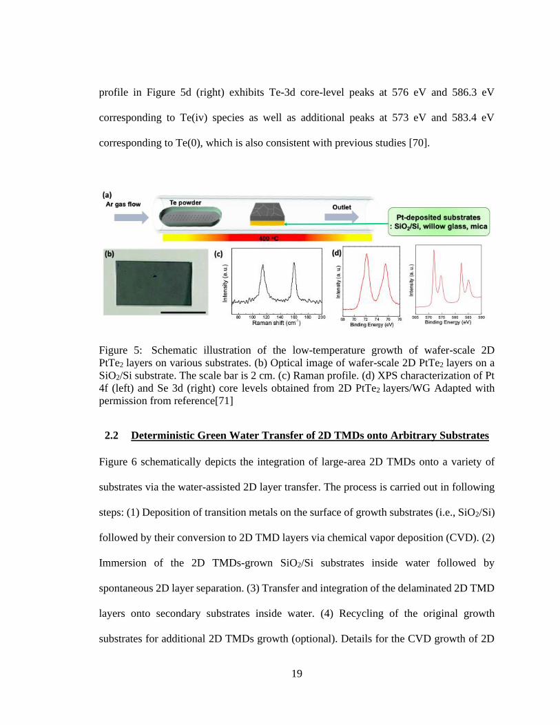
2.2 Deterministic Green Water Transfer of 2D TMDs onto Arbitrary Substrates
Figure 6 schematically depicts the integration of large-area 2D TMDs onto a variety of
substrates via the water-assisted 2D layer transfer. The process is carried out in following
steps: (1) Deposition of transition metals on the surface of growth substrates (i.e., SiO2/Si)
followed by their conversion to 2D TMD layers via chemical vapor deposition (CVD). (2)
Immersion of the 2D TMDs-grown SiO2/Si substrates inside water followed by
spontaneous 2D layer separation. (3) Transfer and integration of the delaminated 2D TMD
layers onto secondary substrates inside water. (4) Recycling of the original growth
substrates for additional 2D TMDs growth (optional). Details for the CVD growth of 2D

20
TMDs are described in Methods section. The water-assisted 2D layer separation can be
carried out in following two slightly different manners. The first method is to slowly
immerse the entire 2D TMDs-grown substrate inside water while the second method is to
deposit water droplet only on the sample surface to leverage its buoyancy. We emphasize
that the whole process utilizes water only without involving any kinds of additional
chemicals for the separation, transfer, and integration of 2D TMD layers. Previous
approaches generally employed the combined use of polymeric protective materials (e.g.,
PMMA or Polyvinyl alcohol (PVA)) and chemical etchants for the removal of SiO2 [66,
72]. In addition to the operational complexity inherent to these conventional approaches,
2D TMDs are susceptible to chemical degradation owing to the corrosive nature of
hydrogen fluoride (HF) or strong bases (sodium or potassium hydroxide (NaOH or KOH))
involved in the processes [73]. Moreover, their structural integrity can be significantly
altered by the solution-based chemicals (e.g., acetone) employed to rinse away the
protective polymers as well as being affected by the polymer residuals. On the other hand,
our water-assisted approach yields the completely clean and homogenous integration of a
variety of 2D TMDs on a large centimeter scale. As this approach is intrinsically free of
introducing chemicals-associated structural damage, the original SiO2/Si substrates after
2D layer separation can be reused for the subsequent growth of additional 2D TMD
materials (step (4) in Figure 6).

21
Figure 6: Schematic to illustrate the water-assisted green integration of CVD-grown 2D
TMD layers on arbitrary substrates. Adapted with permission from reference [74]
Figure 7 shows the successful demonstration of the water-assisted integration of 2D TMDs
onto a variety of unconventional substrates which would be difficult to achieve otherwise.
Figure 7 (a-c) shows the images of centimeter-scale 2D MoS2 layers integrated on a piece
of (a) wood, (b) paper, and (c) cured polydimethylsiloxane (PDMS), respectively. The
results highlight the strength and generality of our water-assisted integration approach
which is insensitive to the kind of acceptor substrates as the entire process is chemically
benign. Figure 7d demonstrates the “layer-by-layer” integration of 2D MoS2 layers on a
piece of polyethylene terephthalate (PET) substrate achieved over an area of ~2 cm2. After
the initial integration of original 2D MoS2 layers (denoted, L0), additional layers prepared
from the identical substrate were subsequently stacked on them, denoted as (L1) and (L2),
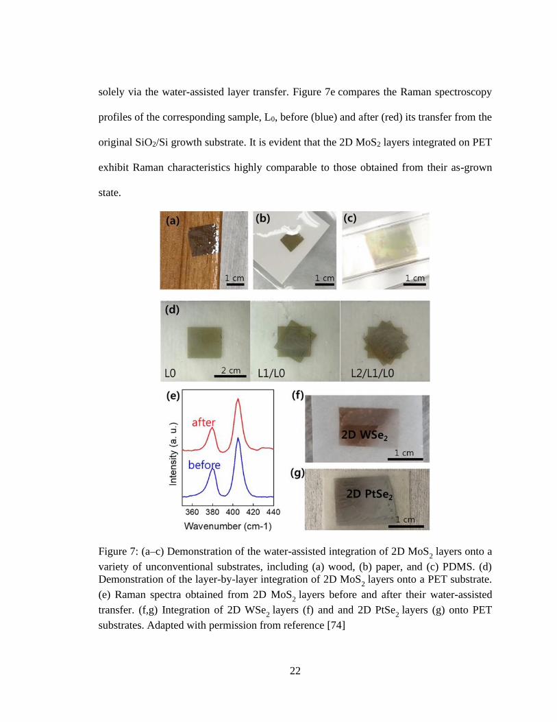
22
solely via the water-assisted layer transfer. Figure 7e compares the Raman spectroscopy
profiles of the corresponding sample, L0, before (blue) and after (red) its transfer from the
original SiO2/Si growth substrate. It is evident that the 2D MoS2 layers integrated on PET
exhibit Raman characteristics highly comparable to those obtained from their as-grown
state.
Figure 7: (a–c) Demonstration of the water-assisted integration of 2D MoS2 layers onto a
variety of unconventional substrates, including (a) wood, (b) paper, and (c) PDMS. (d)
Demonstration of the layer-by-layer integration of 2D MoS2 layers onto a PET substrate.
(e) Raman spectra obtained from 2D MoS2 layers before and after their water-assisted
transfer. (f,g) Integration of 2D WSe2 layers (f) and and 2D PtSe
2 layers (g) onto PET
substrates. Adapted with permission from reference [74]
23
The result evidences the well-retained structural and chemical integrity of 2D MoS2 layers
even integrated on exotic substrates, strongly emphasizing the high reliability, versatility,
and cleanness of the water-assisted transfer method. Moreover, we demonstrate the
generality of this layer transfer approach by extending it to a variety of 2D TMDs beyond
MoS2, including 2D tungsten (W) or platinum (P) diselenides (2D WSe2 and 2D PtSe2).
Figure 7 (f,g) show the images of centimeter-scale CVD-grown 2D WSe2 and 2D
PtSe2 layers transferred and integrated on PET substrates, respectively.
2.3 Conclusion
In conclusion, we present a simple and scalable thermal assisted conversion method for
synthesizing large-scale 2D TMDs on a variety of substrates. We demonstrate the direct
growth of Pt-based TMDs on polymeric substrates owing to their low growth temperature.
Additionally, we report a novel approach to reliably transfer a variety of 2D TMD layers
and heterogeneously integrate them onto virtually arbitrary yet unconventional substrates.
The presented method benefits from the water-assisted spontaneous separation of 2D
layers, exhibiting distinguishable advantages over conventional approaches in terms of
property preservation and size scalability. The intrinsic generality and versatility of this
integration method has been verified with 2D TMDs of various kinds as well as their multi-
component heterostructures. Moreover, its potential for device applications has been
confirmed by demonstrating centimeter-scale 2D MoS2-based flexible photodetectors and
pressure sensors integrated on exotic substrates, which are difficult to fabricate with any
other conventional approaches.

24
CHAPTER 3 PERIODICALLY CORRUGATED MOS2 LAYERS
The contents of this chapter have been published in: Okogbue, E., J. H. Kim, T.-J. Ko, H.-
S. Chung, A. Krishnaprasad, J. C. Flores, S. Nehate, M. G. Kaium, J. B. Park, S.-J. Lee,
K. B. Sundaram, L. Zhai, T. Roy and Y. Jung (2018). "Centimeter-Scale Periodically
Corrugated Few-Layer 2D MoS2 with Tensile Stretch-Driven Tunable
Multifunctionalities." ACS Applied Materials & Interfaces 10(36): 30623-30630.
3.1 Introduction
Two-dimensional (2D) transition metal dichalcogenide (TMD) layers exhibit
superior optical, electrical, and structural properties unattainable in any traditional
materials. Many of these properties are known to be controllable via external mechanical
inputs, benefiting from their extremely small thickness coupled with large in-plane strain
limits. However, realization of such mechanically driven tunability often demands highly
complicated engineering of 2D TMD layer structures, which is difficult to achieve on a
large wafer scale in a controlled manner.
In this chapter, we explore centimeter-scale periodically corrugated 2D TMDs,
particularly 2D MoS2, and report their mechanically tunable multifunctionalities. We used
previously described developed water-assisted process to homogeneously integrate few
layers of 2D MoS2 on three-dimensionally corrugated elastomeric substrates on a large area
(>2 cm2). The evolution of electrical, optical, and structural properties in these three-
dimensionally corrugated 2D MoS2 layers was systematically studied under controlled
tensile stretch. We identified that they present excellent electrical conductivity and
25
photoresponsiveness as well as systematically tunable surface wettability and optical
absorbance even under significant mechanical deformation. These novel three-
dimensionally structured 2D materials are believed to offer exciting opportunities for large-
scale, mechanically deformable devices of various form factors and unprecedented
multifunctionalities.
3.2 Results and Discussions
3.2.1 Synthesis of Periodically Corrugated MoS2 Layers
Figure 8a illustrates the fabrication process of centimeter-scale periodically
corrugated 2D MoS2 layers. The process starts with the preparation of a corrugated
polydimethylsiloxane (PDMS) substrate using a sapphire with periodically (1 μm pitch)
grooved sinusoid structures as the patterning mold. The PDMS is poured and cured on the
mold surface at room temperature for 48 h to ensure its desired surface adhesiveness. Once
peeled off the mold, the prepared PDMS substrate is then biaxially stretched to a certain
extent (e.g., 50% of its original length) using a homemade automated tensile stretcher. A
separately prepared as-grown 2D MoS2 layer on a SiO2/Si substrate is subsequently
integrated on the surface of the pre-stretched PDMS. The 2D MoS2 layers-grown substrate
is mildly pressed against the PDMS to ensure a conformal contact with its surface under
stretching. Subsequently, water droplet is deposited on the growth substrate-integrated
PDMS which is then allowed for a few minutes. The water penetrates into the van der
Waals gaps in between the as-grown 2D MoS2layers and the underlying SiO2, taking
advantages of the imbalance in the surface energies of 2D MoS2 and SiO2. Once the

26
remaining water droplet is completely removed by a paper towel, the integrated SiO2/Si
substrate is gently removed. As a result, only the 2D MoS2 layers become delaminated
preserving their pristine material quality since they were in intimate contact with the
PDMS. Lastly, the pre-applied tensile stretch is released in the PDMS, which yields
periodically corrugated 2D MoS2 layers/PDMS. Previous approaches based on the water-
aided transfer of 2D layers [73, 75], rely on the capillary force for their delamination in
water, which generally leads to the formation of unwanted layer wrinkles and overlaps.
The present approach avoids such drawbacks as the adhesiveness of the PDMS enables the
conformal contact of the entire 2D layer surface as well as achieving a transfer of precisely
defined patterns. Figure 8 (b-e) demonstrates the structural characterization of 2D
MoS2 layers grown on SiO2/Si before their integration to PDMS. The growth was
performed by the CVD sulfurization of pre-deposited Mo (typically, ∼2 nm thickness) ,
the two-step CVD growth method is as previously described in Figure 5. The thickness of
Mo is carefully selected to ensure the growth of 2D MoS2 layers in a horizontal geometry
avoiding unwanted vertical 2D layer orientation [76]. Figure 8b shows the Raman spectrum
of as-grown 2D MoS2 layers on a SiO2/Si substrate (area ∼2 cm2), pictured in the inset.
The Raman profile shows two distinct peaks corresponding to the in-plane (E12g) and out-
of-plane (A1g) vibration modes of 2D MoS2layers [76, 77]. The cross-sectional
transmission electron microscopy (TEM) image of the corresponding sample reveals the
horizontally oriented 2D MoS2 layers of well-resolved 2D layer number (Figure 8c). The
plane-view high-resolution TEM (HRTEM) image in Figure 8d reveals the Moiré pattern
of hexagonal MoS2 basal planes,[78] which is indicative of the lattice misorientation of
stacked layers and is consistent with the cross-sectional TEM. The energy dispersive X-

27
ray spectroscopy (EDS) mapping images of the same sample obtained in a scanning TEM
(STEM) mode show the spatial homogeneity of Mo and S Figure 8e, further confirming
the complete conversion of Mo and S into 2D MoS2 layers [79].
Figure 8: (a) Illustration of the process to fabricate periodically corrugated 2D MoS2 layers
integrated on PDMS. (b) Raman characterization of large-area 2D MoS2 layers grown on
a SiO2/Si substrate along with the corresponding sample image (inset). (c) Cross-sectional
TEM image of as-grown 2D MoS2 with horizontally aligned layers. (d) Plane-view
HRTEM image showing the Moiré fringes from as-grown 2D MoS2 layers. (e) STEM-EDS
maps revealing the uniform spatial distribution of Mo and S. The scale bar is 100 nm (f)
Demonstration of the transfer and integration of 2D MoS2 layers on a pre-stretched PDMS.
Adapted with permission from reference [80]
Figure 8f evidences the viability of the water-assisted integration of 2D
MoS2 layers onto a prepatterned/stretched PDMS, as illustrated in Figure 8a. The top image
demonstrates the application of water droplet on 2D MoS2 layers-grown SiO2/Si attached
on a pre-stretched PDMS, and the bottom image reveals the successful transfer of 2D

28
MoS2 layers only. It is worth mentioning that our integration approach enables a complete
transfer of as-grown, large-area 2D MoS2 layers in their original shape while precisely
replicating the 3D pattern of the secondary substrate.
3.2.2 Structural Characterization
Figure 9 describes the structural characterization of 2D MoS2 layers integrated on
a prepatterned PDMS. Figure 8a, shows a large-area (∼2 cm2) homogeneously continuous
film integrated on a PDMS, revealing distinguishable color compared to the surrounding
PDMS which is optically transparent. The film is indeed confirmed to be 2D MoS2 layers,
characterized by Raman spectroscopy as well as optical absorption measurements. The
enlarged optical image of the red square box reveals the periodically spaced patterns of
continuous 2D MoS2 layers which cover the entire area of targeted integration. Figure 9b
demonstrates the mechanical flexibility/bendability of the 2D MoS2 layers integrated on
PDMS—the same sample as described in Figure 9a. The vivid optical contrast obtained
only from the region of 2D MoS2 layers reflects that they are in the corrugated structure
[81], which is in sharp contrast to the optically transparent PDMS. The projected scanning
electron microscopy (SEM) image Figure 9c confirms the periodically (1 μm pitch)
corrugated 2D MoS2 layers conformally attached to the underlying PDMS. Figure 9d-g
presents the atomic force microscopy (AFM) characterization of the 2D MoS2 layers on
PDMS. Figure 9d,e shows the plane- and projected-view AFM topography profiles of the
same material in Figure 9a and 9b respectively.
29
Figure 9: (a) Optical microscopy images of periodically corrugated 2D MoS2 layers on
PDMS over an area of ∼2 cm2. (b) Image of the same sample in sunlight showing
holographic reflection from the 2D MoS2 layers. (c) Side-view SEM image showing the
periodically corrugated structure of 2D MoS2 layers on PDMS. (d) Top-view AFM
topography image of the same sample. (e) 3D projected AFM topography image of the
same sample revealing the alternating appearance of hills and valleys with a periodicity of
1 μm. (f) AFM adhesion map profile corresponding to (d) and (e). (g) AFM height profile
(blue) and Young’s modulus mapping (red) of the same sample, revealing that the hill
regions are highly strained. Adapted with permission from reference [80]
The bright and dark AFM image contrasts present the periodic appearance of “hill”
and “valley” regions in the corrugated 2D MoS2 layers, respectively, consistent with the
optical and SEM observations. Figure 9f shows a corresponding AFM adhesion map
confirming the conformal coating of 2D MoS2 layers on PDMS, and its quantitative
analysis is presented in Figure 9g. The AFM height profile (red) and Young’s modulus
distribution (blue) Figure 9g across the periodically corrugated 2D MoS2 layers infer that
the hill regions are in the highest strain state. This observation of strain distribution is
consistent with previous studies on the 2D MoS2 layers of wrinkled/crumpled structures
[82, 83]. Moreover, the modulus distribution is observed to be highly periodic and uniform
30
across the repeatedly appearing hills/valleys, further suggesting the structural homogeneity
of the material. In the AFM analysis, the modulus is calculated by using the equation
𝐹𝑡𝑖𝑝 = 4
3𝐸 ∗ √𝑅𝑑3 + 𝐹𝑎𝑑ℎ ( 1 )
where E* is the reduced Young’s modulus, Ftip is the force on the tip, Fadh is the adhesion
force, R is the tip radius, and d is the tip–sample separation [84].
Having confirmed the achievements of large-area, periodically corrugated, and
continuous 2D MoS2 layers on PDMS, we then assess their multifunctional material
properties under controlled mechanical deformation. We systematically characterize their
electrical, optical, and structural properties under unidirectional tensile stretch and evaluate
their strain-driven evolution. Figure 9 a,b shows a representative image of periodically
corrugated 2D MoS2layers on PDMS clamped with an automated mechanical stretcher
which applies tensile stretch at a rate of 0.5 mm/s. In Figure 9a, the as-prepared sample is
initially in a pristine state (AFM and SEM images in Figure 9 c,d) with an original
length L1 along the orientation of the tensile stretch. The sample is then subjected to a
stretch of 50% with a new length L2 = L1+ 0.5L1 (Figure 9b). From the images, it is
confirmed that there is no slippage of the 2D MoS2layers on the underlying PDMS owing
to its high conformity, which is crucial for the proper measurements of material properties.
Moreover, we quantified the surface roughness of corrugated 2D MoS2 layers by
characterizing their topography with AFM and confirmed its gradual reduction with
increasing stretching.

31
3.2.3 Electro-Mechanical Characterization
Having confirmed the excellent mechanical stretchability of corrugated 2D
MoS2 layers, we first characterized their electrical properties under systematically
controlled tensile stretch. Figure 10c shows the two-terminal current (I)–voltage (V)
transport characteristics with varying tensile stretch. The results indicate a very slight
decrease of current with increasing stretching, implying that the corrugated 2D MoS2 layers
well preserve their structural/electrical integrity upon being flattened out. In contrast, the I–
V characteristics from plain 2D MoS2 layers on PDMS without corrugation show a drastic
current decrease with increasing stretching (Figure 10d). We calculate the relative change
of resistance, i.e., ΔR/R0, where ΔR is an increase in resistance R over initial
resistance R0 and plot it in Figure 10e (red dots). The corrugated 2D MoS2 layers present
∼60% increase of ΔR/R0 upon a tensile stretch up to 30%, confirming their excellent
electrical tunability under severe mechanical deformation. It is worth mentioning that
significant electrical failure (i.e., >6000% increase of ΔR/R0) was previously reported in
CVD-grown unstructured 2D MoS2 layers even at a tensile stretch of <∼5% [51]. For
comparison, a plot of resistance change vs stretching level for plain 2D MoS2 layers/PDMS
without corrugation is also presented (Figure 10e, black dot), which shows a much steeper
(>10 times) change in ΔR/R0 under the identical stretch level consistent with previous
studies[85]. We note that there exists a few studies on three-dimensionally crumpled
graphene and other 2D materials and their stretch-driven electrical responses while these
materials are limited to 2D layers of random orientation on small areas[86, 87]. We
emphasize that this study explores 2D MoS2 layers with precisely defined structures on a

32
wafer scale (>2 cm2) and their multifunctionalities, significantly advancing over the
previous studies in terms of dimensional scalability, structural controllability, and the
versatility of tunable properties (to be further discussed). Moreover, we performed fatigue
tests on corrugated 2D MoS2 layers by characterizing their electrical response upon
repeated stretch for a large number of cycles and confirmed excellent mechanical tolerance.
Figure 10: Periodically corrugated 2D MoS2 layers on PDMS in their (a) pristine and (b)
stretched states along with the corresponding schematic illustrations. (c, d) Two-
terminal I–V characteristics with increasing stretching for (c) periodically corrugated and
(d) plain 2D MoS2 layers without corrugation. (e) Comparison of ΔR/R
0 for periodically
corrugated vs plain 2D MoS2 layers. Adapted with permission from reference [80]
3.2.4 Optical and Surface Characterization
Having proved the tunable electrical properties, we also assessed the optical
properties of periodically corrugated 2D MoS2 layers and investigated the influence of
mechanical deformation. We performed the ultraviolet–visible (UV–vis) spectroscopy
characterization of another sample and identified its optical absorbance under varying
tensile stretch levels in a wide range of spectral wavelengths. Figure 11a indicates that the
absorbance monotonically decreases with increasing stretching, which reflects the
reduction in the surface-volume ratio in the given area of the sample[86, 87]. Two

33
absorbance peaks are visible in the spectral range of ∼600–700 nm, which correspond to
A and B excitonic peaks from the K point of the Broullion zone in 2D MoS2 layers[88, 89].
The observed absorbance characteristics are quite consistent with previous studies
revealing distinguishable features of 2D MoS2 layers,[89] which further confirms their
successful large-area transfer/integration on PDMS. Interestingly, we observe that these
excitonic peaks exhibit a systematic blue-shift with increasing stretch levels, manifested
by the reduction in the A excitonic peak energy as shown in Figure 11b. We believe that
this stretch-driven blue-shift is attributed to the “funnel effect” in strained 2D
materials; theoretical/experimental studies on intrinsically and/or extrinsically strained 2D
materials indicate that excitons generated by light illumination drift to the most strained
regions with their layers. Our 2D MoS2 layers are highly strained in their initially
corrugated state, possessing the maximally strained hill regions (AFM modulus in Figure
8g). Increasing tensile stretch across the hills introduces the “relaxation” of this built-in
strain as the initially corrugated 2D MoS2 layers in their highest strain state become
systematically flattened out (Figure 11 a,b). Consequently, 2D MoS2 layers in a more
strained state corresponding to the smaller stretch level in Figure 10a result in significant
recombination of drifted excitons and hence a lower exciton energy[88]. Previous studies
with randomly crumpled graphene have reported similar absorbance tunability driven by
external strain[86], while our materials exhibit a highly systematic trend retained on a
centimeter-scale area owing to their controlled geometry. The stretch-driven tunability of
the optoelectrical properties in corrugated 2D MoS2 layers was further verified by
characterizing their photoresponsiveness. We confirmed dynamic and reversible
photocurrent generation from a sample in a pristine (corrugated) state under repeated

34
optical illumination (Figure 11c)—measured at 10 V with 17 s intervals. Moreover, we
systematically measured alternating on/off photocurrents under increasing stretching levels
with/without optical illumination as shown in Figure 11d–obtained from a sample different
from that for Figure 11c. The result confirms that the on/off photocurrent responsiveness
is well retained even up to the stretch of ∼30% under the illumination of an identical
intensity. The gradual decrease of the photocurrent with increasing stretch is attributed to
the decrease of the optical absorbance (Fig. 11a), i.e., decrease in the number of
photoexcited carriers under a given illumination area.
Figure 11: (a) Optical absorbance spectra of periodically corrugated 2D MoS2 layers on
PDMS under varying stretch levels. A and B excitonic peaks are denoted. (b) Variation of
A excitonic peak energy under varying stretch levels. (c) Dynamic and reversible
photocurrent generation from 2D MoS2 layers on PDMS in a corrugated state. (d) Variation
of on/off photocurrent under varying stretch levels. Adapted with permission from
reference [80]
Moreover, we study the stretch-tunable structural properties of periodically
corrugated 2D MoS2 layers by characterizing their surface wettability through water
contact angle (WCA) measurements. Figure 12 presents the morphological evolution of
water droplet on the surface of corrugated 2D MoS2 layers/PDMS under varying stretch
levels as well as corresponding WCA values. The plots show the excellent hydrophobicity
of the material, and the WCA values are observed to systematically decrease with
increasing stretching levels in the tested range of 0–50%. This trend is attributed to the
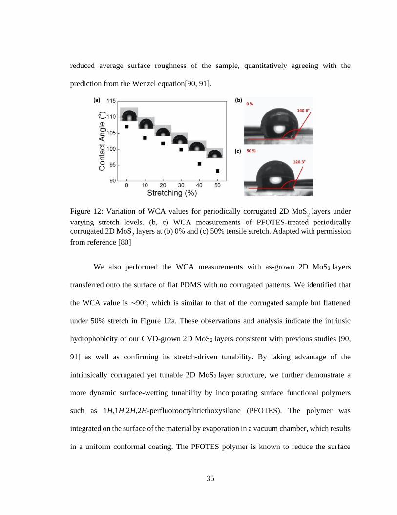
35
reduced average surface roughness of the sample, quantitatively agreeing with the
prediction from the Wenzel equation[90, 91].
Figure 12: Variation of WCA values for periodically corrugated 2D MoS2 layers under
varying stretch levels. (b, c) WCA measurements of PFOTES-treated periodically
corrugated 2D MoS2 layers at (b) 0% and (c) 50% tensile stretch. Adapted with permission
from reference [80]
We also performed the WCA measurements with as-grown 2D MoS2 layers
transferred onto the surface of flat PDMS with no corrugated patterns. We identified that
the WCA value is ∼90°, which is similar to that of the corrugated sample but flattened
under 50% stretch in Figure 12a. These observations and analysis indicate the intrinsic
hydrophobicity of our CVD-grown 2D MoS2 layers consistent with previous studies [90,
91] as well as confirming its stretch-driven tunability. By taking advantage of the
intrinsically corrugated yet tunable 2D MoS2 layer structure, we further demonstrate a
more dynamic surface-wetting tunability by incorporating surface functional polymers
such as 1H,1H,2H,2H-perfluorooctyltriethoxysilane (PFOTES). The polymer was
integrated on the surface of the material by evaporation in a vacuum chamber, which results
in a uniform conformal coating. The PFOTES polymer is known to reduce the surface

36
energy of materials, resulting in superhydrophobic surface wettability[92]. Figure 12 b,c
show the WCA measurements of the PFOTES-treated, periodically corrugated 2D
MoS2 layers in their pristine state (WCA ∼ 141° at 0%) and after a tensile stretch (WCA
∼ 120° at 50%), respectively.
3.3 Conclusion
In summary, we developed a reliable process to transfer and integrate large-area 2D
MoS2 layers on pre-structured elastomeric polymers. This transfer/integration approach
overcomes the intrinsic limitations of previously developed crumpled 2D MoS2 layers in
terms of achieving the scalable controllability of tailored dimension and targeted
geometries. The comprehensive measurements of electrical, optical, optoelectrical, and
structural properties in the periodically corrugated 2D MoS2 layers testify their high
versatility for realizing a large set of dynamically tunable multifunctionalities.

37
CHAPTER 4 MULTIFUNCTIONAL 2D PtSe2-LAYER
KIRIGAMI CONDUCTORS
The content of this chapter have been published in : Okogbue, E., S. S. Han, T.-J. Ko, H.-
S. Chung, J. Ma, M. S. Shawkat, J. H. Kim, J. H. Kim, E. Ji, K. H. Oh, L. Zhai, G.-H. Lee
and Y. Jung (2019). "Multifunctional Two-Dimensional PtSe2-Layer Kirigami Conductors
with 2000% Stretchability and Metallic-to-Semiconducting Tunability." Nano Letters
19(11): 7598-7607
4.1 Introduction
Although intrinsically large strain limits are projected in them (i.e., several times
greater than silicon), integrating 2D TMDs in their pristine forms does not realize superior
mechanical tolerance greatly demanded in high-end stretchable and foldable devices of
unconventional form factors. In this chapter, we report a versatile and rational strategy to
convert 2D TMDs of limited mechanical tolerance to tailored 3D structures with extremely
large mechanical stretchability accompanying well-preserved electrical integrity and
modulated transport properties. We employed a concept of strain engineering inspired by
an ancient paper-cutting art, known as kirigami patterning, and developed 2D TMD-based
kirigami electrical conductors. Specifically, we directly integrated 2D platinum diselenide
(2D PtSe2) layers of controlled carrier transport characteristics on mechanically flexible
polyimide (PI) substrates by taking advantage of their low synthesis temperature. The
metallic 2D PtSe2/PI kirigami patterns of optimized dimensions exhibit an extremely large
stretchability of ∼2000% without compromising their intrinsic electrical conductance.
They also present strain-tunable and reversible photoresponsiveness when interfaced with
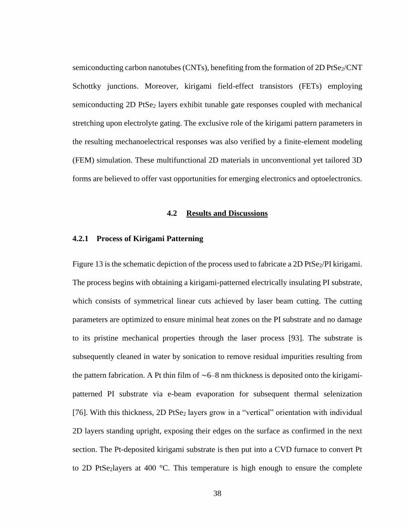
38
semiconducting carbon nanotubes (CNTs), benefiting from the formation of 2D PtSe2/CNT
Schottky junctions. Moreover, kirigami field-effect transistors (FETs) employing
semiconducting 2D PtSe2 layers exhibit tunable gate responses coupled with mechanical
stretching upon electrolyte gating. The exclusive role of the kirigami pattern parameters in
the resulting mechanoelectrical responses was also verified by a finite-element modeling
(FEM) simulation. These multifunctional 2D materials in unconventional yet tailored 3D
forms are believed to offer vast opportunities for emerging electronics and optoelectronics.
4.2 Results and Discussions
4.2.1 Process of Kirigami Patterning
Figure 13 is the schematic depiction of the process used to fabricate a 2D PtSe2/PI kirigami.
The process begins with obtaining a kirigami-patterned electrically insulating PI substrate,
which consists of symmetrical linear cuts achieved by laser beam cutting. The cutting
parameters are optimized to ensure minimal heat zones on the PI substrate and no damage
to its pristine mechanical properties through the laser process [93]. The substrate is
subsequently cleaned in water by sonication to remove residual impurities resulting from
the pattern fabrication. A Pt thin film of ∼6–8 nm thickness is deposited onto the kirigami-
patterned PI substrate via e-beam evaporation for subsequent thermal selenization
[76]. With this thickness, 2D PtSe2 layers grow in a “vertical” orientation with individual
2D layers standing upright, exposing their edges on the surface as confirmed in the next
section. The Pt-deposited kirigami substrate is then put into a CVD furnace to convert Pt
to 2D PtSe2layers at 400 °C. This temperature is high enough to ensure the complete
39
thermal selenization of Pt [94, 95] and is low enough not to deform the underlying PI
substrate. Finally, gold (Au) contacts are deposited on the two ends of the 2D PtSe2/PI
kirigami for electrical characterization under tensile stretching. During the stretching
process, the kirigami pattern leads to a reduction in its in-plane stiffness, causing the out-
of-plane buckling of constituting struts allowing for high elasticity as depicted in the
scheme (verified in a later section).
Figure 13: Schematic of the fabrication processes for kirigami-patterned, vertically aligned
2D PtSe2 layers on a flexible PI substrate. Adapted with permission from reference [96]
4.2.2 Structural Characterization
Before evaluating the mechanoelectrical performance of 2D PtSe2/PI kirigami
patterns, we first confirmed the successful growth of 2D PtSe2 layers on PI substrates by
characterizing their as-grown morphology. We employed a variety of characterization
techniques including X-ray photoelectron spectroscopy (XPS), transmission electron
microscopy (TEM), and energy-dispersive X-ray spectroscopy (EDS). Figure 14a shows
an image of a bare PI substrate (left) and a Pt-deposited PI substrate after CVD selenization
(right), revealing distinguishable color contrast. We identified the chemical composition of

40
the Pt-deposited PI substrate which underwent CVD selenization. Figure 14b shows the
XPS core-level spectra of Pt 4f and Se 3d obtained from the Pt-deposited PI substrates after
CVD selenization and their corresponding spin–orbit splitting values of 3.3 and 1.1 eV,
respectively. As shown in Figure 14b, the Pt 4f spectrum was featured to present a high
symmetry of the spectral profiles with a narrow full width at half-maximum of ∼1 eV.
Moreover, Pt 4f exhibits no observable signal produced by elemental Pt (the expected
position of Pt 4f7/2 is ∼71 eV), indicating that the entire spectrum can be assigned to
Pt4+ corresponding to PtSe2. Se 3d spectra can be deconvoluted into two chemical states,
as presented in Figure 13c. The predominant spectrum represents PtSe2, whose spin-up
state (j = 2 + 1/2) is located at 54.1 eV. On the other hand, the humplike small peak centered
at ∼58.6 eV is associated with the oxidation of Se to SeO2 or SeO3 [97]. The EDS mapping
images in Figure 14d confirm the highly homogeneous spatial distribution of Pt and Se,
indicating the complete conversion of Pt and Se to PtSe2. Figure 14e shows a high-
resolution TEM (HRTEM) image of the sample corresponding to Figure 14d. The image
reveals that the material consists of multiple domains of vertically aligned 2D PtSe2 layers
in various crystallographic orientation exposing their 2D edge sites on the surface. Figure
14f is the corresponding scanning TEM (STEM) image revealing vertically aligned 2D
PtSe2 layer edges with an interlayer spacing of ∼0.54 nm. This value corresponds to the
(001) crystalline plane of 2D PtSe2 layers, as illustrated in the schematic of their atomic
structures[98, 99]. The cross-sectional TEM image directly confirms the successful growth
of vertically aligned 2D PtSe2 layers on PI substrates identifying their thickness as ∼30 nm

41
Figure 14: (a) Camera images showing a bare PI (left) and an as-grown 2D PtSe2 layers-
on-PI substrate prepared by the CVD selenization of 8 nm Pt (right). (b and c) XPS
characterization of (b) Pt 4f and (c) Se 3d core levels obtained from 2D PtSe2 layers on PI
substrates. (d) EDS mapping images obtained from the corresponding 2D PtSe2 layers. (e)
HRTEM image of the corresponding sample showing vertically aligned 2D PtSe2 layers
along with their schematic illustration (inset). (f) STEM image showing the edges of
vertically aligned 2D PtSe2 layers with an interlayer spacing of ∼0.54 nm, corresponding
to the schematic illustration in the inset. Adapted with permission from reference [96]
4.2.3 Electro-Mechanical Characterization
Having confirmed the successful fabrication of 2D PtSe2/PI kirigami patterns
enabled by the low-temperature direct growth of 2D PtSe2 layers, we investigated their
mechanoelectrical properties. In designing the kirigami pattern, we considered the
geometrical and dimensional influences of the pattern on the resulting electrical properties
(d)
(f)
(e)
(c)(b)(a)

42
under mechanical deformation. We attempted to maximize the retention of electrical
conductance under tensile stretch by applying optimized parameters to the kirigami pattern
design. The schematic in Figure 15a presents the kirigami pattern of symmetrical linear
cuts where key characteristic parameters are defined as follows: a is the cut length, b is the
spacing between two cuts perpendicular to the direction of tensile force, and c is the
vertical spacing between the linear cuts parallel to the direction of tensile force. On the
basis of the beam theory which models the mechanical deflection of a strut[100, 101], the
relationship between the critical tensile force (F) and the characteristic parameters is given
as
𝐹 ∝ 𝐸𝑐𝑡3
(𝑎−𝑏)3 ( 2 )
where E is Young’s modulus and t is the thickness of the strut as deflection occurs along
its length. The equation indicates that an increase in the cut length leads to a reduction in
the critical buckling length, thereby allowing for continued elongation along the direction
of applied force. Similarly, decreasing the vertical and horizontal spacing improves the
maximum attainability of strain. Note that the strain is defined as ε = Δl/lo, where lo is the
initial length of the kirigami before stretching and Δl is the increase in the length upon
stretching. The maximum strain attainable by the kirigami is proportional the cut
length a and is inversely proportional to the lateral and vertical spacing of b and c, while
the number of columns and rows within the pattern has a negligible impact[100].
Considering the above relationship between the maximum strain and characteristic
parameters, we applied the following parameters to achieve maximum lateral stretchability
in the 2D PtSe2/PI kirigami and investigated its resulting electrical properties upon

43
stretching: a = 17.2 mm, b = 0.4 mm, and c = 0.375 mm. Figure 15a shows the current
response of a 2D PtSe2/PI kirigami pattern with these parameters under varying strain
levels applied by manual stretching. The kirigami pattern exhibits a negligible current drop
of ≲5% even up to 2000% strain, confirming its excellent electrical retention. Figure 15b
shows the two-terminal current–voltage (I–V) characteristics of the corresponding sample
revealing the ohmic nature of metallic 2D PtSe2layers as manifested by the high linearity
of I–V. We note that this 2000% retention achieved with 2D PtSe2 layer-based kirigami is
orders of magnitude higher than the stretchability of other experimentally demonstrated 2D
MoS2 layer-based kirigami patterns [102] and outperforms most of the state-of-the-art
kirigami-patterned electrical conductors [100, 103, 104]. We then investigated the failure
characteristics of kirigami patterns, for which we employed the in-situ monitoring of
current–strain variation until their electrical breakdown. We first manually stretched
another sample to 1000% strain and loaded it into an automated tensile stretcher before
applying controlled strain. Figure 15c shows that the sample exhibits an electrical failure
at ∼2350% strain accompanying a drastic current drop within ∼5% before the failure point.
The inset of the figure corresponds to the red-boxed regime detailing the failure
characteristics. For further assessment of the strain-invariant electrical stability of kirigami
patterns, we performed cyclic tests by repeatedly stretching and releasing them up to a
fixed strain. Figure 15d presents the current variation of another kirigami sample
undergoing a large number of cyclic stretching—up to 1000 times at 1000% strain. The
result confirms the excellent mechanical stability of the kirigami in terms of retaining its
original electrical conductance throughout severe mechanical deformation. It is worth
mentioning that previously developed nanomaterials-based kirigami patterns are mostly
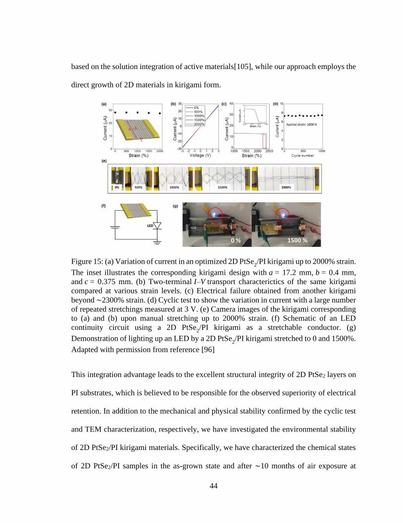
44
based on the solution integration of active materials[105], while our approach employs the
direct growth of 2D materials in kirigami form.
Figure 15: (a) Variation of current in an optimized 2D PtSe2/PI kirigami up to 2000% strain.
The inset illustrates the corresponding kirigami design with a = 17.2 mm, b = 0.4 mm,
and c = 0.375 mm. (b) Two-terminal I–V transport characterictics of the same kirigami
compared at various strain levels. (c) Electrical failure obtained from another kirigami
beyond ∼2300% strain. (d) Cyclic test to show the variation in current with a large number
of repeated stretchings measured at 3 V. (e) Camera images of the kirigami corresponding
to (a) and (b) upon manual stretching up to 2000% strain. (f) Schematic of an LED
continuity circuit using a 2D PtSe2/PI kirigami as a stretchable conductor. (g)
Demonstration of lighting up an LED by a 2D PtSe2/PI kirigami stretched to 0 and 1500%.
Adapted with permission from reference [96]
This integration advantage leads to the excellent structural integrity of 2D PtSe2 layers on
PI substrates, which is believed to be responsible for the observed superiority of electrical
retention. In addition to the mechanical and physical stability confirmed by the cyclic test
and TEM characterization, respectively, we have investigated the environmental stability
of 2D PtSe2/PI kirigami materials. Specifically, we have characterized the chemical states
of 2D PtSe2/PI samples in the as-grown state and after ∼10 months of air exposure at

45
ambient temperature and compared their characteristics. XPS characterization identifies
that the envelopes of both Pt 4f spectra are nearly identical, which indicates that the
4+ valence state of Pt is well retained even after prolonged air exposure. The shapes of Se
3d spectra pertaining to PtSe2 are also very similar to a slight reduction in SeOx.
Having proven the superior structural and electrical integrity of 2D PtSe2/PI
kirigami materials, we explored their potential applications which take advantage of strain-
invariant metallic transports. We first utilized them as stretchable conductors for operating
small electronic devices for which we demonstrated the powering up of a light emitting
diode (LED), as illustrated in Figure 15f. The optimized 2D PtSe2/PI kirigami used for
Figure 15e was connected to an LED light and was stretched from 0 to 1500% by an
automated tensile stretcher. Figure 15g demonstrates that the light intensity (2 W/m2) of
the LED remains unchanged even up to 1500% strain (denoted by the red circles in both
figures), indicating unimpaired charge transports in 2D PtSe2 layers.
4.2.4 Opto-Electrical Properties
In addition to the application for stretchable and foldable electrical conductors, we
further explored unconventional opportunities for 2D PtSe2/PI kirigami by combining it
with other functional materials. The metallic nature of vertically aligned 2D PtSe2 layers
confirmed by the FET characterization indicates the feasibility of forming Schottky
junctions when they are interfaced with semiconducting materials. In this approach, we
considered semiconducting carbon nanotubes (CNTs) with intrinsically excellent
mechanical flexibility suitable for kirigami integration.
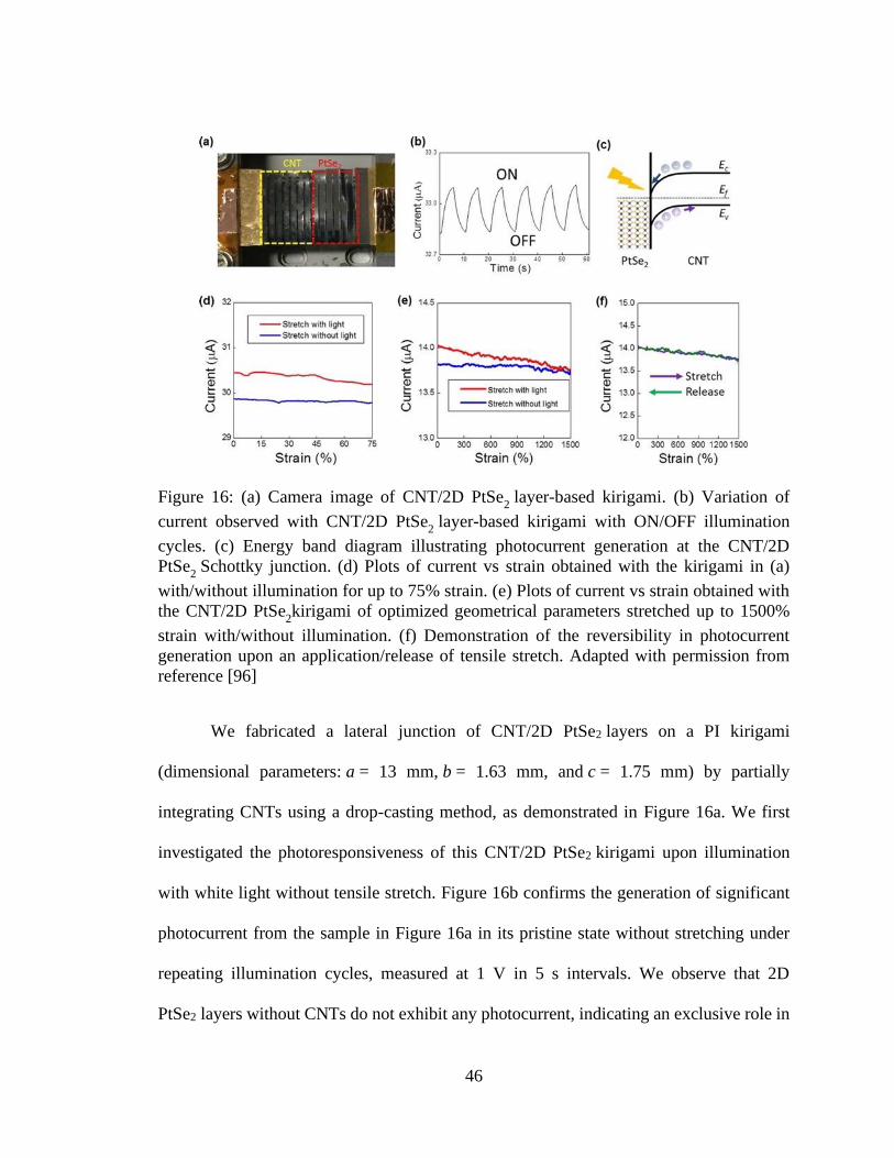
46
Figure 16: (a) Camera image of CNT/2D PtSe2 layer-based kirigami. (b) Variation of
current observed with CNT/2D PtSe2 layer-based kirigami with ON/OFF illumination
cycles. (c) Energy band diagram illustrating photocurrent generation at the CNT/2D
PtSe2 Schottky junction. (d) Plots of current vs strain obtained with the kirigami in (a)
with/without illumination for up to 75% strain. (e) Plots of current vs strain obtained with
the CNT/2D PtSe2kirigami of optimized geometrical parameters stretched up to 1500%
strain with/without illumination. (f) Demonstration of the reversibility in photocurrent
generation upon an application/release of tensile stretch. Adapted with permission from
reference [96]
We fabricated a lateral junction of CNT/2D PtSe2 layers on a PI kirigami
(dimensional parameters: a = 13 mm, b = 1.63 mm, and c = 1.75 mm) by partially
integrating CNTs using a drop-casting method, as demonstrated in Figure 16a. We first
investigated the photoresponsiveness of this CNT/2D PtSe2 kirigami upon illumination
with white light without tensile stretch. Figure 16b confirms the generation of significant
photocurrent from the sample in Figure 16a in its pristine state without stretching under
repeating illumination cycles, measured at 1 V in 5 s intervals. We observe that 2D
PtSe2 layers without CNTs do not exhibit any photocurrent, indicating an exclusive role in

47
the electronic junction of CNT/2D PtSe2 layers upon its generation. The mechanism for
photocurrent generation is attributed to the Schottky junction of CNT (semiconducting)/2D
PtSe2 layers (metallic), which is very similar to the case of the photocurrent generation in
CNT–graphene junctions. Figure 15c illustrates an approximate energy band diagram to
depict the formation of a CNT/2D PtSe2 Schottky junction where a band-gap energy of
∼0.6 eV is assigned for the CNT used in this study as known from previous reports. From
the diagram, it is apparent that illumination with a white light generates and separates
photocarriers, leading to an efficient separation and collection of the majority of carriers
across the Schottky barrier. Qualitatively, similar photocurrent generation has been
observed with CNT/graphene junctions, benefiting from the metallic transport of graphene
layers as similar to 2D PtSe2 layers. After confirming the photocurrent generation in the
CNT/2D PtSe2 kirigami in its pristine form (sample in Figure 16a) we then applied a tensile
stretch to it and investigated the resulting photoresponsiveness. Figure 16d compares the
electrical responses of the CNT/2D PtSe2 kirigami for up to the 75% strain level with and
without illumination. Substantial photocurrent was observed under illumination measured
at 0.5 V throughout the stretch, indicating the well-retained electrical and structural
integrity of the CNT/2D PtSe2 Schottky junction. We also tested another CNT/2D
PtSe2kirigami with optimized geometrical parameters and higher stretchability
corresponding to Figure 16a. Figure 16e compares the photoresponsiveness of the kirigami
under a tensile stretch of up to 1500% strain with/without illumination. Significant
photocurrent was generated under illumination, and it gradually decreases with increasing
stretch levels, which is attributed to the decrease in the surface area of the kirigami exposed
under illumination. Note that the illumination area from the optical source remains constant

48
throughout the tensile stretch, leading to the decrease in the active surface area for
absorbing incident photons upon the continued elongation of the kirigami. Moreover, we
tested the reversibility of the strain-tunable photocurrent generation in this kirigami under
reversible mechanical deformation. Figure 16f compares the electrical responses from the
same kirigami stretched to 1500% and shrunk back to 0% as controlled by an automated
tensile stretcher under illumination of constant intensity (165 W/cm2). The results show
nearly identical values of photocurrent under stretching and shrinking at a given strain
level, confirming the excellent reversibility of strain-tunable electrical/optical properties.
4.2.5 Finite Element Simulations
To clarify the mechanism behind the excellent strain-invariant electrical
performance of 2D PtSe2 layer-based kirigami patterns, we employed FEM simulation and
studied the geometrical effects of kirigami patterns on the strain distribution introduced by
a tensile stretch. We studied the patterns of two different configurations (i.e., unoptimized
parameters of a = 6.5 mm, b = 1.63 mm, c = 1.75 mm and optimized parameters of a =
17.2 mm, b = 0.4 mm, and c = 0.375 mm as shown in the left and right schematics in Figure
17a, respectively). FEM simulation images used to describe the spatial distribution of
“global” strain on the unoptimized vs optimized patterns under stretching are presented in
Figure 17b,c respectively. The unoptimized pattern in Figure 17b shows that the large
vertical and horizontal spacings (band c) between the struts limit their torsional rotation,
causing a high strain concentration at the cut edges even at a low strain level of λ ≈ 1.6; λ
is the stretch coefficient defined by λ = l/lo, where lo and l denote the length before and

49
after the stretch, respectively. On the other hand, upon stretching the kirigami with
optimized parameters (Figure 17c), the applied tensile force causes the pattern to readily
rotate around the cut edges (orange and yellow boxes) of high strain localization. This
rotation results in an efficient relaxation of accumulating strain, preserving the intrinsic
electrical conduction with λ being much larger than that observed with the unoptimized
kirigami.
Figure 17: (a) Schematics showing the defining geometrical parameters for the
unoptimized (left) vs optimized (right) kirigami patterns. (b, c) FEM simulations showing
the strain distribution within the kirigami patterns of (b) unoptimized and (c) optimized
parameters. (d) Graphical comparison of maximum in-plane principal strain vs stretch for
the unoptimized (blue plot) vs optimized (red plot) kirigami patterns. The inset compares
the simulated vs experimentally demonstrated images of kirigami patterns while their
failure point is approximated to be ∼0.1 times the maximum in-plane principal strain. (e–
g) Plots of maximum in-plane principal strain vs stretch with varying geometrical
parameters of (e) a, (f) b, and (g) c. Adapted with permission from reference [96]
Figure 17d compares the maximum in-plane principal strain values as a function of
λ for the unoptimized vs optimized patterns. The maximum in-plane principal values are
obtained from the edge cut areas of higher local strain presented in Figure 17b,c. Because
kirigami patterns present complex strain tensors owing to their multidirectional
deformation, the maximum in-plane principal strain was chosen for performance

50
comparison. It is noted that significantly smaller maximum in-plane principal strain is
realized in the optimized pattern at a given λ, suggesting its high stretchability until the
failure point of >0.1. Moreover, the optical images of the experimentally realized kirigami
patterns (insets; colored in gray) look nearly identical to the simulated ones, indicating the
excellent controllability of our patterning process. It is noteworthy that the major motive
for presenting the two cases of “unoptimized” vs “optimized” patterns is to demonstrate
the controllability of lateral stretching in the kirigami patterns by rationally defining the
dimensional parameters. The criterion for achieving a large degree of stretchability is to
increase the length (a) of constituting trusts and simultaneously decreasing their widths
(band c). Accordingly, the failure point of the kirigami should appear at λ of a much larger
value, which corresponds to larger stretchability. The unoptimized kirigami pattern
electrically breaks down at ∼75% strain as experimentally observed (which is significantly
smaller than that achieved with the optimized pattern (Figure 17e) as predicted above. To
further demonstrate the role of kirigami pattern designs on controlling the resultant
performance, we have carried out additional FEM simulations by varying the dimensional
parameters of a, b, and c in eq 2. Figure 17e-g shows the variation of maximum in-plane
principal strain with varying a, b, and c, respectively. The analysis confirms that the stretch
levels corresponding to the approximately defined failure point of 0.1 maximum in-plane
principal strain drastically increase with larger a and smaller b and c. This observation
indicates that the kirigami pattern can be significantly more stretched (e.g., up to ∼4000%)
over what we have experimentally demonstrated by further adjusting the dimensional
parameters. In this work, we have judiciously and intentionally selected the optimized
parameters of a, b, and c and achieved the maximum stretchability of >2000% to avoid the

51
technical difficulty associated with manually handling samples with b and c parameters
that are too small. In the FEM simulation, we have considered that kirigami patterns exhibit
a varying Poisson ratio during the course of their structural change.
4.2.6 Application for Stretchable Transistor
Finally, we further explored the application aspects of 2D PtSe2/PI kirigami
patterns by taking advantage of the tunable electrical properties of 2D PtSe2 layers of
precisely controlled morphology. Two-dimensional PtSe2 layers exhibit a semiconducting-
to-metallic transition as their layer morphology and thickness vary, as modulated by CVD
growth conditions [98, 106] (i.e., vertically aligned thick 2D PtSe2 layers exhibit metallic
transport while horizontally aligned thin layers are semiconducting [107]). While the above
demonstrations (Figure 16 and 17) focus on utilizing the metallic transport of 2D
PtSe2 layers, we further extend the kirigami approach to exploit their semiconducting
properties in unconventional electronic applications, including kirigami FETs. To this end,
we grew semiconducting 2D PtSe2 layers in the horizontal orientation by selenizing Pt of
small thickness (typically <1 nm) under CVD conditions identical to those mentioned
above[107]. Figure 18a shows a HRTEM image of horizontally aligned 2D PtSe2 layers
directly grown on PI revealing multiple crystalline grains and Moiré fringes.
Corresponding cross-sectional TEM and EDS characterization further confirm their
stoichiometric growth maintaining the horizontal-layer orientation. Prior to exploring the
kirigami FET applications, we first carried out control experiments to verify the intrinsic

52
carrier type of the horizontally aligned 2D PtSe2 layers by characterizing FET gate
responses.
Figure 18: (a) HRTEM image of horizontally aligned thin 2D PtSe2 layers. (b) I
ds–
Vds
transfer characteristics from a back-gated FET based on horizontally aligned thin 2D
PtSe2 layers configured on a SiO
2/Si wafer. (c) Schematic illustration of an electrolyte
gating of a 2D PtSe2/PI FET. (d) I
ds–V
g and (e) I
ds–V
ds transfer characteristics from a 2D
PtSe2/PI FET. The scale bar in the inset of (d) is 1 mm. (f) I
ds–V
g transfer characteristics
from a 2D PtSe2/PI kirigami FET. (g) Camera images of the kirigami FETs corresponding
to (f). Adapted with permission from reference [96]
Figure 18b presents the transfer characteristics of drain-source current vs voltage
(Ids–Vds) with varying gate voltage (Vg) from a back-gated FET configured on a SiO2/Si
substrate (inset). The plots reveal p-type semiconducting FET gate responses (i.e.,
increasing Ids with decreasing Vg at a given Vds). Having confirmed the “intrinsic”
semiconducting nature of horizontally aligned 2D PtSe2layers, we then attempted to

53
develop FETs incorporating them on PI substrates and eventually their kirigami forms. For
the reliable operation of FETs even under mechanical stretching, we employed electrolyte
gates (e.g., potassium chloride (KCl)) as a medium to gate the devices as shown in Figure
18c. Horizontally aligned 2D PtSe2 layers on PI substrates were in top contact with metal
electrodes for source-drain patterns which were electrically isolated by
poly(dimethylsiloxane) (PDMS). Then, a droplet of KCl (10 mM) was applied on top of
the 2D PtSe2 layers, and it was electrically biased for gating. Figure 18d shows the Ids–Vg
transfer characteristics of an electrolyte-gated 2D PtSe2/PI FET (device image in the inset),
and Figure 18e presents its corresponding Ids–Vg transfer characteristics with
varying Vg.These characterization results confirm the reliable gate response of 2D PtSe2/PI
FETs, offering a basis for extending them in kirigami form. The identical electrolyte gating
approach was applied to 2D PtSe2/PI kirigami FETs, and Figure 17f exhibits Ids–Vg transfer
characteristics from a kirigami sample of varying stretch levels. The plots clearly reveal
that p-type semiconducting transports are well retained with slightly decreasing Ids during
the increasing mechanical stretch. Figure 18g shows the images of the kirigami FETs
corresponding to Figure 18f where PDMS is used as a chamber to contain KCl of constant
concentration (10 mM). It is worth mentioning that our finding of the strain-invariant Ids–
Vgtransfer characteristics qualitatively agrees with the observation with the graphene
kirigami FETs [108] of smaller dimensions gated under similar electrolyte conditions.
4.3 Conclusion
We have developed a multifunctional 2D PtSe2/PI kirigami which exhibits strain-invariable
electrical conductance and strain-tunable photoresponsiveness. Metallic 2D PtSe2 kirigami

54
patterns of optimized dimensions and geometries presented excellent electrical retention
up to ∼2000% tensile stretch, significantly outperforming previously explored other
nanomaterial-based stretchable electrical conductors. Moreover, they presented
substantive photocurrent modulation which was reversibly retained throughout significant
mechanical deformation. Kirigami FETs were realized by utilizing semiconducting 2D
PtSe2 layers and exhibited electrolyte-driven tunable gate responses under mechanical
stretching. This unconventional type of 2D material configured in 3D form offers exciting
opportunities for futuristic stretchable and foldable electronics.
55
CHAPTER 5 SMART WEARABLE DEVICES BASED ON Pt-
TMDs
The content of this chapter have been published in :
Dmitry Kireev, Emmanuel Okogbue, Jayanth RT, Tae-Jun Ko, Yeonwoong Jung, Deji
Akinwande “Multipurpose and Reusable Ultrathin Electronic Tattoos based on PtSe2 and
PtTe2”, ACS Nano 2021, 15, 2, 2800-2811
Tae-Jun Ko, Sang Sub Han, Emmanuel Okogbue, Mashiyat Sumaiya Shawkat, Mengjing
Wang, Jinwoo Ma, Tae-Sung Bae, Shihab Bin Hafiz, Dong-Kyun Ko, Hee-Suk Chung, Kyu
Hwan Oh, Yeonwoong Jung “Wafer-Scale 2D PTte2 Layers-Enabled Kirigami Heaters
with Superior Mechanical Stretchability and Electro-Thermal Responsiveness”, Materials
Today, 2020, 20, 100718
5.1 Introduction
Platinum is one of the most stable metals from the group 10 materials and is considered to
be a noble metal (along with gold). It is well known for its resistance to corrosion[109],
catalytic properties[110], and excellent biocompatibility[111]. Pt is frequently used in
fundamental research and industrial applications as an electrode, catalyst, etc.
Consequently, the Pt-based TMDs were theoretically expected and have practically been
proven to have excellent air- and water- stability[112], compared to other TMDs. Pt-TMDs
typically feature thickness-dependent semiconductor-to-metal transition, excellent ambient
stability, and low synthesis temperature[96]. Such properties make them as prime
candidates when it comes to the development of bioelectronic or wearable devices. The
direct growth of 2D TMDs on ultrathin polyimide allows fabrication of flexible materials

56
with unique electronic properties that have high prospects of being the future building
blocks of next-generation wearable devices. PtSe2 and PtTe2 are considered promising for
numerous bioelectronic applications and so far, none has been practically realized.
In this chapter, we show that PtSe2 and PtTe2 can be used to develop multipurpose
wearable electronics devices for healthcare related applications. As an ideal bioelectronic
wearable material that features excellent in-plane current conduction, as well as out-of-
plane conduction, PtTe2 is found to outperform PtSe2. In terms of electrical conductivity,
skin-contact, and electrochemical impedance, PtTe2 even outperforms graphene electronic
tattoos [113], and performs on par or even better than classical Ag/AgCl gel electrodes,
regardless almost 10-fold smaller area. Both of the materials, PtSe2 and PtTe2, outperform
graphene in terms of electronic contact to skin. The skin impedance-based electrode
characterization data is supplemented with the electrical impedance spectroscopy
measurements that prove the same: the atomically thin PtTe2 is an excellent material for
future bioelectronic applications, such as possible use for neural probes for chronic in vivo
characterization. Additionally, we will showcase several applications of the Pt-TMDs for
numerous wearable healthcare applications including measurement of electromyograms
(EMG, muscle contractions), electrooculogram (EOG), electrocardiogram (ECG) and
electroencephalogram (EEG, brainwaves), that are essential aspects of hospital-based
biopotential monitoring systems, especially during times of fatal disease-treatments.
Furthermore, we explore the electrothermal properties of chemically grown 2D PtTe2
layers and demonstrate their application for high-performance extremely stretchable
wearable heaters. We characterized their electrical properties and identified intrinsically
small sheet resistance down to 19.4 Ω/□, significantly smaller than those of previously
57
developed any other 2D materials. By taking this combined advantage of low growth
temperature and high electrical conductance, we developed 2D PtTe2 layers-based
stretchable and wearable heaters by directly growing them on strain-engineered polymeric
substrates of Kirigami forms and evaluated their electrothermal performances.
5.2 Kirigami-Patterned Wearable Heater
5.2.1 Electrothermal Properties of PtTe2 Layers
To pursue this projected opportunity, we first demonstrated the direct growth of 2D
PtTe2 layers on mechanically flexible PI substrates. By applying the identical CVD recipe
adopted for SiO2/Si as growth substrates, we grew 2D PtTe2 layers on PI substrates which
are highly stable even above 400 °C. Figure 19a shows optical images of as-grown 2D
PtTe2 layers on PI substrates prepared with Pt films of varying thickness, revealing
decreasing optical transparency with increasing thickness. Electrothermal properties of
these samples were characterized by identifying their temperature variation upon an
application of electrical biasing, determined by IR imaging. Figure 19b presents a diagram
that correlates the maximum temperature (Tmax) of 2D PtTe2/PI samples prepared with
varying Pt thickness obtained at three different applied voltages. Tmax steadily increases
with increasing thicknesses due to lower sheet resistance as predicted by the Joule-heating
efficiency equation (P = V2/Rs). Indeed, we note that the electrically-driven temperature
change of these samples well follows the Joule-heating efficiency equation irrespective of
their thicknes. Particularly, we observe that these 2D PtTe2/PI heaters exhibit significantly
high temperature even at very low operation voltages, e.g., ~170 °C for PtTe2-9 nm at 7 V,

58
much lower than the voltage regarded as non-hazardous according to International
Electrotechnical Commission (IEC 60950-1).
Figure 19: (a) Photos of 2D PtTe2 layers-grown flexible PI substrates prepared with Pt films
of various thicknesses. (b) The maximum temperature of 2D PtTe2/PI samples prepared
with various Pt thickness achieved at biases of 3, 5, and 7 V. (c) Time-dependent
temperature fall/rise of the same samples in (b) obtained at 5 V. (d) Determination of the
heating/cooling rate corresponding to (c). (e) Temperature variation obtained from a 2D
PtTe2-6nm/PI sample during the cyclic heating/cooling of 50 times at 4 V. (f)
Representative IR images of the sample in (e) at three different cycle numbers. (g)
Demonstration of the solar energy-driven operation of 2D PtTe2/PI heaters. (h)
Temperature variations achieved with 2D PtTe2/PI heaters of various thickness driven by
solar energy. Adapted with permission from reference [114]
Figure 19c shows the time-dependent variation of Tmax for 2D PtTe2 layers prepared with
varying Pt thickness operated at a constant voltage of 5 V for 30 sec. Upon the

59
onset/termination of the voltage denoted by the first/second dashed lines,
respectively, Tmax rapidly increases/decreases within 10 secs for all samples. Figure 19d
presents the first derivatives of the time-temperature plots in Figure 19c, clarifying the
heating/cooling kinetics of the 2D PtTe2 layers more precisely. The PtTe2-9nm sample
exhibits the heating/cooling rate of 26.6 °C/sec and 24.2 °C/sec under 5 V, respectively,
which allows the heater to reach Tmax much faster (5 sec) than that obtained with other
nanomaterials previously explored for heater applications, e.g., nano graphite, or reduced
graphene oxide (rGO)[115]. These heating/cooling rates can be further increased to 46.8
°C/sec and 36.6 °C/sec by applying a higher voltage of 7 V, respectively, achieving
significantly faster thermal responses - Supporting Information, Figs. S5b-e. Moreover, we
also evaluated the electrothermal endurance of these samples by applying/terminating a
constant voltage in a cyclic manner and identifying resulting temperature variation. The
plot of cycle number vs. temperature in Figure 18e presents the cyclic heating/cooling of
an identical sample (i.e., 2D PtTe2-6nm) obtained under a cyclic application/termination of
4 V for 50 times. Considering the fast heating/cooling rate of the sample for
achieving Tmax/ambient temperature, a fixed interval of 10 sec was assigned for the voltage
application/termination in each cycle. It is noteworthy that the average Tmax of 81.9 °C is
well retained throughout the entire cyclic period accompanying a very small deviation of
~1.0 °C, confirming excellent electrothermal endurance essential for practical
applications. Figure 19f presents IR images of the same sample in Figure18e, obtained at
specific periods of 1st, 25th, and 50th cycles, showing the stable operation with multiple
cycles. Furthermore, in a way to assess the technological potential of 2D PtTe2/PI materials
as a portable heater for practical applications, we characterized their electrothermal

60
performances driven by solar energy. Figure 19g shows a representative image (left) of a
2D PtTe2-6nm sample connected to a portable solar panel and its corresponding IR images
without (mid) and with (right) sunlight illumination. Figure 19h presents the variation of
temperature for the samples of various thickness operated at ~4 V driven by solar energy.
(Air mass: ~1.3, Ambient temperature ~30 °C) It is noteworthy the 2D PtTe2-6nm sample
reaches Tmax of 53.0 °C in its ON state (with illumination), which is > ~25 °C increase
compared to its OFF state (without illumination). All these results comprehensively
indicate that 2D PtTe2 layers possess a large set of electrothermal properties essential for
high-performance heating devices, i.e., low operational voltage, rapid responsiveness as
well as high thermal stability and endurance.
5.2.2 Fabrication and Characterization of Kirigami Patterned Heater.
Encouraged by these intrinsically superior electrothermal properties and deformation-
insensitive structural integrity inherent to 2D PtTe2 layers, we set on exploring them for
skin-attachable flexible heaters. To this end, it is particularly essential to configure the 2D
PtTe2/PI heaters in mechanically stretchable forms well to suit the demands of complex
human body motions. Notably, recent studies suggested that stretchability up to at least
70% is demanded to accommodate maximum human body linear elongation into wearable
device technologies [116]. Various strain engineering schemes employing judiciously
designed patterns and structures have been explored to achieve strain-invariant properties
in stretchable devices, which includes wavy, island-interconnect, and Kirigami geometries

61
[117, 118]. Adopting these pattern-based strategies to the wearable heater application, we
developed strain-invariant 2D PtTe2/PI heaters by employing the concept of Kirigami
pattern designing and evaluated their electrothermal performances under varying stretch
levels. Kirigami patterning approaches inspired the ancient paper-cutting arts have been
employed to efficiently relieve externally applied tensile stress within 2D objects by
converting it to 3D torsional stress. Figure 20a shows the schematic illustration of
fabrication procedures for Kirigami-patterned 2D PtTe2/PI stretchable heaters. Kirigami
patterns containing periodic uni-directional cuts were fabricated on a PI substrate by a
mechanical cutting machine, which was designed to accommodate large stretchability [96].
Subsequently, Pt was deposited on the patterned PI, followed by the above-described CVD
thermal tellurization, which yielded the Kirigami-patterned 2D PtTe2/PI. Lastly, gold (Au)
electrodes were deposited on both ends of the Kirigami-patterned 2D PtTe2/PI for electrical
measurements under mechanical stretching. A simple Kirigami pattern composed of
periodic straight cut lines perpendicular to stretching direction was adopted in this work.
Figure 20b illustrates the schematic of the corresponding Kirigami pattern specifying
geometrical parameters; a is the length of the cut, b is the spacing between two cuts in the
transverse direction, and c is the spacing in the longitudinal direction. We then
experimentally demonstrated electrothermal performances of 2D PtTe2/PI Kirigami heaters
under varying tensile stretch conditions and compared them to the FEM predictions. The
insets in Figure 19c show the representative IR images of a Kirigami-patterned 2D PtTe2-
9nm/PI sample (initial size; 18 × 12 mm2) in a range of 3 to 10 V under varying stretch
levels.
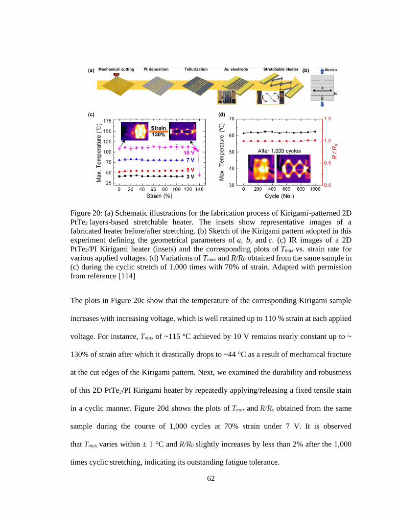
62
Figure 20: (a) Schematic illustrations for the fabrication process of Kirigami-patterned 2D
PtTe2 layers-based stretchable heater. The insets show representative images of a
fabricated heater before/after stretching. (b) Sketch of the Kirigami pattern adopted in this
experiment defining the geometrical parameters of a, b, and c. (c) IR images of a 2D
PtTe2/PI Kirigami heater (insets) and the corresponding plots of Tmax vs. strain rate for
various applied voltages. (d) Variations of Tmax and R/R0 obtained from the same sample in
(c) during the cyclic stretch of 1,000 times with 70% of strain. Adapted with permission
from reference [114]
The plots in Figure 20c show that the temperature of the corresponding Kirigami sample
increases with increasing voltage, which is well retained up to 110 % strain at each applied
voltage. For instance, Tmax of ~115 °C achieved by 10 V remains nearly constant up to ~
130% of strain after which it drastically drops to ~44 °C as a result of mechanical fracture
at the cut edges of the Kirigami pattern. Next, we examined the durability and robustness
of this 2D PtTe2/PI Kirigami heater by repeatedly applying/releasing a fixed tensile stain
in a cyclic manner. Figure 20d shows the plots of Tmax and R/Ro obtained from the same
sample during the course of 1,000 cycles at 70% strain under 7 V. It is observed
that Tmax varies within ± 1 °C and R/R0 slightly increases by less than 2% after the 1,000
times cyclic stretching, indicating its outstanding fatigue tolerance.
63
5.3 Multipurpose and Reusable Atomically Thin Electronic Tattoos based on
PtSe2 and PtTe2
5.3.1 Fabrication of Pt-TMD Tattoos
PtSe2 and PtTe2 used in this work are grown by a thermal-assisted conversion (TAC)-based
chemical vapor deposition (CVD) process. The growth is performed at moderately low
temperatures, at about 400 °C, allowing us to grow the material directly on top of select
polymers[96]. A classic temperature-stable polymer commonly used in bioelectronic
applications is Kapton, known for its mechanical and temperature stability. In this work,
we use two kinds of Pt-TMD tattoos: some are grown directly over Kapton, others are
grown on SiO2/Si wafers and then transferred onto an ultrathin temporary tattoo form
utilizing mechanical support of a 200 nm thick (PMMA) layer [119]. The TAC process
requires platinum to be pre-deposited on the samples’ surface (Figure 21a). We use 6 nm
thick Pt as the material source for Kapton structures and 3 nm thick Pt as the source for
SiO2/Si growth material. The 6 nm thick Pt samples, post-CVD growth, result in ∼25 ± 3
nm thick multilayer Pt-TMD that features multiple out-of-plane growth planes. The 3 nm
thick samples typically result in ∼15 ± 3 nm thick layered dichalcogenide, with a more
uniform in-plane layered arrangement, which has been deemed beneficial for PMMA-
supported tattoo material. After the CVD growth is performed (Figure 21b), the Kapton-
based samples are ready for final processing. The PMMA- and Kapton-based Pt-TMD
tattoos are finally cut into desired shapes by means of a cutter-plotter tool (Silhouette
Cameo). The PMMA-based tattoos are just slightly scribed, while the Kapton-based
samples are cut through their thickness. The Kapton samples are also fixed onto thermal
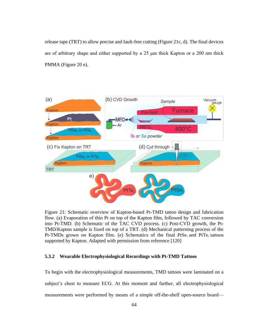
64
release tape (TRT) to allow precise and fault-free cutting (Figure 21c, d). The final devices
are of arbitrary shape and either supported by a 25 μm thick Kapton or a 200 nm thick
PMMA (Figure 20 e).
Figure 21: Schematic overview of Kapton-based Pt-TMD tattoo design and fabrication
flow. (a) Evaporation of thin Pt on top of the Kapton film, followed by TAC conversion
into Pt-TMD. (b) Schematic of the TAC CVD process. (c) Post-CVD growth, the Pt-
TMD/Kapton sample is fixed on top of a TRT. (d) Mechanical patterning process of the
Pt-TMDs grown on Kapton film. (e) Schematics of the final PtSe2 and PtTe2 tattoos
supported by Kapton. Adapted with permission from reference [120]
5.3.2 Wearable Electrophysiological Recordings with Pt-TMD Tattoos
To begin with the electrophysiological measurements, TMD tattoos were laminated on a
subject’s chest to measure ECG. At this moment and further, all electrophysiological
measurements were performed by means of a simple off-the-shelf open-source board—

65
Ganglion from OpenBCI. In the case of ECG recordings, one pair of Pt-TMD tattoos were
placed on the chest, as schematically shown in Figure 22a. Another couple of Ag/AgCl
gel electrodes were placed nearby with similar spacing to provide a direct signal
comparison (see Figure 22a). A reference ground-driven electrode was placed over the
lower right of the abdomen. The signals were sampled at 200 Hz and later filtered with a
60 Hz notch filter to remove the power line noise. The ECG signals measured with
Ag/AgCl and PtTe2 are shown in Figure 22 b,c with clearly present characteristic ECG
peaks (P, Q, R, S, T)[121]. The signal-to-noise ratio (SNR) of PtTe2 tattoo-based
recordings was as high as 84 ± 6, while the nearby Ag/AgCl gel electrodes yielded 61 ± 5.
PtSe2 tattoos’ performance is slightly lower, yet the SNR of 44 ± 4 is high enough to
provide relevant signal information and shape, especially considering the 12-fold
difference in the electrode size. Moreover, ECG can be recorded in a less sophisticated way
by placing two tattoos on opposite hands (e.g., forearms) and a single reference electrode
near a bone (e.g., elbow).
EMG is a distinct, powerful, and useful electrical signal that corresponds to the muscles’
physical contractions within the body [122]. When a pair of electrodes biased in a
differential manner are placed over a muscle, the muscular contractions will generate a net
electrical potential. Typically, the larger the distance between the two electrodes, the larger
the differential signal recorded from the pair. In order to record useful EMG signals, we
placed a pair of Pt-TMD tattoos on a forearm and another pair of tattoos on a bicep, along
with the pairs of Ag/AgCl electrodes for direct comparison (see schematics on Figure 22
d). During a series of forearm contractions (mechanical expander) and bicep curls, we
clearly distinguished those movements via simple monitoring of the EMG activity and the

66
signal’s power. One can see that the signal power from gel electrodes is higher compared
to that for Pt-TMDs, which is due to 12 times larger electrode area as well as the almost 5
times higher spacing between the electrodes. Nonetheless, as it can be seen from Figure
22d for PtTe2, we are able to optimally recognize both: movements of the forearm and
bicep as well as differentiate between them. On the brighter side, Pt-TMD electrodes
feature lower noise, essentially displaying higher signal specificity, equalizing the
performance. The higher signal specificity of Pt-TMD tattoos here relates to superior
adhesion to skin. Mechanical movements push the large gel electrodes to move physically,
creating motion artifacts, that contribute to higher noise. As can be seen from the timetrace
of consecutive bicep and forearm movements (see Figure 22d), often, the muscular
movement associated with a bicep curl also results in slight forearm muscle contractions,
which is always picked up by the large Ag/AgCl gel electrodes. These nonspecific signals
usually obstruct from making clear and decisive interfacing, and as it is evident from the
results provided, smaller Pt-TMD tattoos suffer much less from this problem.
The low contact electrode–skin impedance displayed by Pt-TMDs is essential for most
electrophysiological measurements but especially for EEG. EEG signals are electrical
signals associated with the ever-active electrical activities inside the brain[123]. There is a
broad scientific community working on EEG and its applications, mostly studying the
correlations between EEG signals and the underlying brain functions. Developing a tattoo
system that can be used for EEG recordings (a) reliably, (b) with intimate contact and signal
quality, and (c) reusable is a high-impact task. To measure EEG signals, a couple of Pt-
TMD tattoos were placed on the subject’s forehead, precisely onto the Fp1 and Fp2
locations, and sampled separately with a common ground electrode connected to an

67
earlobe. The EEG recordings were typically collected over a period of 120–240 s and
featured specific patterns of subjects’ activities—their eyes being open or closed. After
applying the short-time Fourier transformation (STFT) onto the recorded signals, the
output spectrogram, as shown in Figure 22e, reveals the heatmap of signal frequency
components and their power levels (in dB), distributed over the entire timetrace. It is well-
known that EEG, recorded from the forehead, should show prevailing α waves (8–13 Hz)
when the subject’s eyes are closed, especially at the Fp1 and Fp2 locations. As seen from
Figure 22e, the spectrogram patterns pick up the α waves when “eyes closed” with
PtTe2 and PtSe2 tattoos and Ag/AgCl gel electrodes. To specifically show the statistical
presence of α rhythms, we have averaged and plotted the spectral power density from gel,
PtSe2, and PtTe2 electrodes with open and closed eye intervals show that there is a
significant power density peak around 8–13 Hz that corresponds to the α waves when “eyes
closed”, yet the peak is absent in the case of “eyes open”.
To showcase a human–machine interface enabled by the Pt-TMD tattoos, we measured
electrical signals associated with the eye movements, which could easily be later channeled
into a computer, robot, or machine[124]. EOGs are very similar to the EMG signals but are
associated with the differences in polarization of the eye’s cornea and retina. To record
EOG signals, we have placed four Pt-TMDs on a subject’s face: one pair goes above and
below the left eye, one tattoo on the left side of the left eye, and the last tattoo on the right
side of the right eye (see Figure 23a for details).

68
Figure 22: Wearable electrophysiological recordings with Pt-TMDs. (a) Schematic of the
electrode placement for the ECG measurement. (b) Five-second-long ECG timetrace from
PtTe2 tattoos and Ag/AgCl gel electrodes. (c) Average ECG signal shapes, amplitudes, and
average SNRs for PtTe2 tattoo and Ag/AgCl gel electrode. (d) Schematic of electrode
placement and EMG recordings from a human’s bicep (top) and forearm (bottom) muscle
contractions recorded via the Ag/Ag gel electrodes and PtTe2 tattoos simultaneously. The
horizontal bars on the top and bottom mark the events and durations of the bicep curls and
forearm contractions correspondingly. (e) Electrode placement for EEG measurements
(left) and resulting spectrogram (right) from one of the PtTe2 tattoos placed on the Fp1 and
Fp2 locations on the subject’s forehead. Adapted with permission from reference [120]
The tattoos placed on the sides of the eyes are connected differentially into a single channel,
and the electrodes above and below the left eye are connected differentially to the other
channel. When the subject is looking into a particular direction, specific cornea–retina
depolarization events create electric potential differences associated with the movement.

69
As seen from the timetrace recordings (see Figure 23b), gazing left and right results in the
distinct change of the appropriate channel’s EOG signal. Similarly, gazing up and down
results in a specific pattern recorded by another pair of electrodes (see Figure 23c).
Figure 23: (a) Schematic of the electrode placement for the EOG experiments performed
with PtTe2 tattoos. (b) EOG signals corresponding to the differential channel recording
left–right eye movements (violet here and after). (c) EOG signals corresponding to the
differential channel recording up–down eye movements (green here and after). (d) EOG
recordings from both channels when the subject is gazing up, right, right, left, down, down,
and left consecutively with 5 s dwell time. (e) EOG recordings from both channels when
the subject is looking counterclockwise with four distinct stops: at “12”, “9”, “6”, and “3”
o’clock. Straight and angular arrows in (d,e) correspondingly show the direction of sight.
Adapted with permission from reference [120]
When slower gazing experiments are performed, a clear differentiation can be made
between various gazing patterns (e.g., up–down, up–center, left–center, center–right, etc.).
There is, however, a certain “overshoot” signal that can be seen in some recordings (see
Figure 23b, c) when the eyes are returning from a peripheral into straight positions.
However, these “overshoots” are directional and help distinguish the change of sight
70
direction in dynamics. Figure 23d shows the results of an elaborate, nonroutine experiment
when the subject was instructed to look into the direction as conducted by the experimenter,
online and without any warning. It is visible that the patterns for looking down, up, left,
and right can be discretely identified. Such a pattern is readily distinguishable, allowing us
to differentiate between arbitrary directions. Eye blinks do cause some troubles and create
certain events, mainly in the up–down channel, yet they can be later postprocessed and
removed[125].
In the final EOG experiment, the subject was instructed to perform more sophisticated eye
movements that are not just fixed to one degree of freedom (straight horizontal or straight
vertical) as before. Here, the subject performed circular eye movements (like looking over
a watch) counterclockwise with four distinct stops: at 12, 9, 6, and 3 o’clock positions.
Astonishingly, those movements resemble a combination of the aforementioned two-
degree movements. For example, when moving from 12 to 9, the recorded signal pattern is
a combination of the signals corresponding to “left” and “down” (see Figure 23e for
details). The results clearly indicate that the TMD tattoos can constitute a technology that
does advanced eye-tracking for human–machine interfaces.
5.4 Conclusion
In conclusion, we presented works on high-quality advanced wearable and bioelectronic
devices based on Pt-TMDs, namely PtSe2 and PtTe2. Both PtSe2 and PtTe2 possess high
conductivity desirable for wearable and implantable electrode. We explored PtTe2 layers
for high-performance mechanically deformable heaters by employing their intrinsically
superior mechanical, electrical, and thermal properties. PtTe2 layers directly grown on

71
large PI substrates at 400 °C exhibited excellent Joule heating efficiency – i.e., the fast rise
of high temperature at a given voltage – superior to those of previously explored all other
state-of-the-art nanomaterials. Furthermore, we prepared for them in the form of
judiciously designed Kirigami patterns and demonstrated high-performance skin-
attachable heaters, which exhibited strain invariant electrothermal properties and large
stretchability. In terms of electrode–skin impedance, a figure-of-merit for wearable
electrode systems, Pt-TMDs outperform graphene-based electronic tattoos, state-of-the-art
noble metal tattoos, and medical-grade gel electrodes. The tattoos are ultrathin, form
intimate contact with skin, and can be made via direct temperature conversion of Pt on top
of polymer substrates. Brainwaves, heart function, muscle activity, skin temperature, and
even eye-tracking are shown to be accurately captured by means of Pt-TMD electronic
tattoos. The eye-tracking is of particular interest as it applies to wearable human–machine
interfaces. We have successfully used two of the pairs of PtTe2 and PtSe2 tattoos built on
Kapton film for all electrophysiology modalities reported in this work, including EEG,
EMG, ECG, and EOG, highlighting their reusability and versatility.

72
CHAPTER 6 PtTe2-BASED BIOMORPH ACTUATORS
6.1 Introduction
Recently, soft actuators have been widely studied owing to their high flexibility and
adaptability[126]. In comparison to their conventional rigid counterparts’ soft actuators are
lightweight and deformable allowing them to achieve multi-degree-of-freedom, and high
load-to-weight ratio[127]. As an important branch, biomorph actuators have received a lot
of research interest over the past few years owing to their simplistic structure, prominent
actuation performance and universal adaptivity[128, 129]. They typically consist of a
hybrid structure of two layers of materials with different thermal expansion behaviors
which generates bending displacement owing to the asymmetric thermal expansion. The
actuation performance from such biomorph actuators is hence generally influenced by the
mismatch of the coefficient of thermal expansion (CTE) of the two material layers. To
obtain soft biomorph electrothermal actuators, non-conductive polymers are usually used
as the structural layer for large deformation, and conductive paths are used as resistive
heaters. Conductive paths are usually obtained by mixing conductive materials with
polymer matrices to form conductive composites having tailored conductivity. Widely
used materials include carbon nanotubes (CNTs), graphene, nanowires due to their intrinsic
high flexibility and conductivity [129-134]. Most of the reported electrothermal actuators
reported involve mixing of the nanomaterials with polymer matrices to change their
thermal, mechanical or electrical properties. These actuators require complicated process
methods and have limited controllability over the heater geometry, and placement on the
soft actuator which are critical for high performance.
In this chapter, we designed and fabricated soft electrothermal actuators based on
directly grown ultrathin PtTe2 layers. Polyimide and polydimethylsiloxane (PDMS) were
selected as the two structural materials for the bimorph configuration due to the large
mismatch in their thermal expansion properties. We directly grew large-scale PtTe2 layers
as heater on the mechanically flexible PI substrates via a thermally assisted conversion
(TAC) process at 400 oC. PDMS layer is then deposited on the 2D PtTe2 heater leading to
the PDMS/2D PtTe2/PI biomorph structure. The direct growth allows for complete

73
coverage, good adhesion, and proper placement of the PtTe2 layers in the heater
configuration. The designed biomorph actuator with excellent performance provides a
promising foundation for construction of biomimetic devices based on 2D TMDs with
multifunctional applications. As a demonstration, soft grippers are designed employing the
PDMS/2D PtTe2/PI soft biomorph actuator as ‘fingers’ to mimic humanoid motion. It has
full capability to lift and manipulate an object that is more than 2 times its own weight in
a very short time (4 seconds).
6.2 Results and Discussions
6.2.1 Fabrication of PDMS/PtTe2/PI Biomorph Actuator
In the design of our soft electrothermal actuator, the biomorph structure was made with
thin films of PI and PDMS owing to the large mismatch in their thermal expansion
capability which can potentially produce large deformation when there is a temperature
change in the actuator. PDMS has a high CTE of ~ 3 x 10⁻⁴ oC-1 which is ten times larger
than that of PI with CTE of 20 x 10-6 oC-1 [135]. The heating element of the biomorph
electrothermal actuator is 2D PtTe2 which is directly grown and embedded in-between the
PI and PDMS layers. A more detailed fabrication process to obtain the PDMS/PtTe2/PI
biomorph actuator is shown in Figure 24a. The process begins with the direct growth of
PtTe2 layers on polyimide substrate, which is carried out in two steps; Pt films of controlled
thickness are deposited on a 25 μm PI substrate (Dupont Kapton) which is followed by
thermal assisted conversion (tellurization) at 400 oC, as reported in our previous
works[136]. This temperature is high enough for the conversion of the Pt seed layers to
PtTe2, and lower than the melting point of the underlying PI substrate. The direct growth
of the PtTe2 layers on the PI substrate owing to the low growth temperature, ensures better

74
adhesion to the underlying substrate as well as good coverage and placement [71]. The
growth of the PtTe2 layers is followed by the deposition of gold film of thickness ~ 150 nm
for electrical contact. The next step in the fabrication process is selective deposition and
curing of PDMS on the as-grown PtTe2/PI. The thickness of the PDMS is controlled using
a wet-film applicator rod (Paul N. Gardner company, Inc) with specified grooving which
leaves behind a film of specified thickness. For selective placement of the PDMS, the gold
contacts are properly covered during the deposition process. The deposited PDMS has a
thickness of ~ 200 μm, this optimal value is obtained through theoretical estimates
explained in the next section. After curing of the PDMS, the PDMS/PtTe2/PI biomorph
actuator stack is cut into a U-shaped configuration for the purpose of forming a current
circuit for electrothermal stimulation.
Figure 24: Schematic of the fabrication process for the PDMS/PtTe2/PI soft bimorph
actuator. (b) Digital image showing the U-shaped PDMS/PtTe2/PI bimorph actuator.
Schematic showing the (c) top and (d) side view profile of the and schematic showing the
top view (middle) and side view profile (bottom) of the PDMS/PtTe2/PI bimorph actuator
dimensions.
Figure 24b (top) shows a digital image of the resulting U-shaped PDMS/PtTe2/PI bimorph
actuator; the length and width dimensions of the entire sample was 25 x 5 mm2 (length x

75
width), wherein the width of the beams are 2 mm and the total thickness of ~ 225 μm. The
detailed dimensions for the U-shaped PDMS/PtTe2/PI actuator are shown in Figure 24 c,d.
6.2.2 Electrothermal Performance and Bending Characterization
After the confirmation of high quality 2D PtTe2 layers and the successful fabrication of the
PDMS/PtTe2/PI soft bimorph actuator, we went ahead to characterize the electrothermal
and actuation properties of the device. The electrode ends of the PDMS/PtTe2/PI actuator
are placed on the edge of glass side for support and are connected to a DC regulated power
supply for electrical characterizations using copper tape. Figure 25a (top) shows optical
images of the device before voltage is supplied (left), with voltage turned on (middle) and
with voltage turned off (right). Additionally, during these different voltage conditions, the
temperatures are being monitored through thermographs as obtained by an IR camera
(FLIR). The PDMS/PtTe2/PI soft bimorph actuator shows a little bending downwards
without the voltage and while at room temperature (Figure 25a (left)). When a voltage of
15 V is applied onto the PDMS/PtTe2/PI soft bimorph actuator, the PtTe2 layers quickly
convert the electrical current into thermal energy through Joule heating as shown in the
thermograph (Figure 25a (middle)). This increase in the temperature from ~ 25 oC (room
temperature) to ~ 117.4 oC leads to mismatched expansion in the PDMS and PI layers to
generate a displacement of 10mm. The displacement is measured by using a ruler, which
can be used to measure such displacements that exceed the range of typical laser
displacement sensors. When the voltage is turned off, the PtTe2 heaters quickly returns
76
back to room temperature and the PDMS/PtTe2/PI soft bimorph actuator returns back to its
original position showing reversibility of the actuation.
It is important to note that the other factor that significantly influences the bending
performance of the actuator is the thickness of each layers in the biomorph structure. The
bending actuation of biomorph structures has been extensively studied and there are there
are theoretical equations to calculate the bending curvature of a bi-layer actuator when
subjected to uniform heating. To determine the optimal thickness of the PDMS, we
employed the bending curvature equation as follows:
𝑘 = 6 (ɣ2− ɣ1)(1+𝑚)2∆𝑇
𝑎(3(1+𝑚)2+(1+𝑚𝑛)(𝑚2+1
𝑚𝑛) (3)
where k is the curvature, Ɣ1 and Ɣ2 are the CTEs of PI and PDMS respectively, a = t1 + t2,
m = t1/t2 where t1 and t2 are the thicknesses of PI and PDMS respectively, n = E1/ E2 where
E1 and E2 are the Young’s modulus of PI and PDMS, ∆T represents the change in
temperature in oC.
Using the equation above (Eq.3), the optimal thickness of the layers of the actuator can be
estimated theoretically. For our actuator design, the thickness of the PI is fixed at 25 μm as
it was commercially purchased, this thickness was chosen for its combination of structural
integrity for handling and flexibility. On the other hand, we obtained the optimal thickness
of PDMS layer through theoretical estimates. Since the overall thickness of our PtTe2
layers is ~ 30 nm i.e., ~ 5 times the thickness of the Pt seed layer (6 nm), as established
from our previous works[114, 120], we assume it does not significantly affect the
curvature. By varying the thickness of the coated PDMS layer, and for a particular
temperature change, we are able to theoretically estimate the bending curvature against
thickness of PDMS. Given the other variables are constant, the maximum temperature
change is achieved when the thickness of the PDMS layer is ~ 200 um. If the PDMS layer
is too thin, enough stretching force cannot be generated to bend the PI layer, on the other

77
hand, if the PDMS layer is too thick, the overall actuation will be dominated by thermal
expansion rather than bending.
Figure 25: Characterization of the bending performance of the actuator (a,b) Optical images
of the PtTe2/PI actuator in a suspended geometry at different time moments when
(a)Voltage is turned on and (b) Voltage is turned off (c) Maximum curvature achieved at
different voltages (d) The resulting actuation curvature over repetitive cycles at applied
voltage of 20V (e) Cyclic graph of maximum curvature of the actuator up to 50 cycles
with applied voltage of 20V.
Figure 25b presents the voltage-dependent temperature of the PDMS/PtTe2/PI soft bimorph
actuator. The relationship between the achieved maximum temperature and the voltage
applied is approximately linear. The highest working temperature of the bimorph actuator
is ~ 160 oC which is below the maximum service temperature of PDMS and PI (~ 250 oC
and > 400 oC respectively), ensuring long service life of the actuator. Along with the
temperature change at different voltages, the PDMS/PtTe2/PI soft bimorph actuator also
undergoes different displacements due to different levels of expansion (Figure 25c). Figure
S3 shows the generated actuation displacement and corresponding thermograph as
6 8 10 12 14 16 18 20
40
60
80
100
120
140
160
180
Te
mp
era
ture
(o
C)
Voltage (V)
6 8 10 12 14 16 18 200
2
4
6
8
10
12
14
Dis
pla
ce
me
nt
(mm
)
Voltage (V)
(b) (c)
1 cm
(a)
20 oC 60 oC 150 oC 60 oC20 oC 20 oC

78
obtained from the IR camera under application of 6 V, 9 V and 15 V. The relationship
between the maximum displacement and the voltage up to 20 V is also approximately
linear, similar to the that observed in Figure 25b.
To investigate the biomorph actuation process of the PtTe2/PI soft actuator, we
characterized the bending performance, as shown in Figure 26. The bending actuation
performance of the PtTe2/PI actuator was demonstrated in a suspended geometry as shown
in side-view optical images in Figure 26(a,b). The fixed end of the actuator was attached
to two electrodes and the bending movement is characterized by a digital camera. The
biomorph is shows a vertical orientation without application of voltage (Figure 3a (left)).
Upon application of voltage, along with the increase in temperature, the soft actuator
underwent bending deformation. Figure 26a (middle) shows the gradual bending status of
the actuator when the electrodes are supplied with 20 V for 2 seconds, there is bending
towards the PDMS side to generate a displacement of ~ 5 mm and a curvature of about ~
0.37 cm -1. The displacement is measured by the rule below which is captured from the
digital camera record, while the curvature is measured using an image processing software
(FIJI) with dedicated curvature analysis plugin (Kappa)[137]. When 20V is applied for 4
seconds, the device is further displaced to ~ 10mm and bends upward and reaches a
maximum curvature of ~ 1.2 cm -1. The generated actuation motion achieved by the device
is larger and faster than most previously reported electrothermal actuators [131, 133, 138-
141]. We observed the curvature of the PtTe2/Pi bimorph actuator at different voltages as
shown in Figure 3c. Similar to the trend of displacement as measured in Figure 2c, there is
increasing curvature as the voltage is increased due to a corresponding increase in
temperature with the curvature ranging from 0.48 to 1.2 cm-1 at applied voltage of 12 V
and 20 V respectively. Furthermore, the bending performance with cycled voltage on and
off are monitored in Figure 26d. When 20 V is applied the PtTe2/Pi biomorph, the generated
bending displacement increases to the maximum in ~ 4 secs and remains curved until the
voltage is turned off (Figure 26d). After the voltage is turned off, sample recovers in about
4 seconds returning to its original uncurved state. For the two actuation cycles, the
displacement curves are identical showing good repeatability from the device. We also

79
tested obtained the maximum curvature for up to 50 cycles with an applied voltage of 20
V (Figure 26e). The graph shows that the actuation motion of the PDMS/PtTe2/PI
biomorph device is reversible and reproducible indicating that the actuator remains elastic.
Figure 26: Characterization of the bending performance of the actuator (a,b) Optical images
of the PtTe2/PI actuator in a suspended geometry at different time moments when
(a)Voltage is turned on and (b) Voltage is turned off (c) Maximum curvature achieved at
different voltages (d) The resulting actuation curvature over repetitive cycles at applied
voltage of 20V (e) Cyclic graph of maximum curvature of the actuator up to 50 cycles
with applied voltage of 20V.
6.2.3 Fabrication of Soft Bi-finger Bimorph Gripper Based on PtTe2
The PtTe2/PI with repeatable large displacement response upon application of voltage
provides a basis for various design and applications[129, 142, 143]. Soft gripping using
soft actuators have been explored due to their adaptability, large deformation and gentle
interaction with the objects. As a demonstration, we fabricated a bi-finger soft gripper by
arranging two PtTe2/PI electrothermal actuators in a series circuit as shown in Figure 27a.
The two actuators are connected together using copper tapes and are connected to a DC
power supply using alligator clips. Figure 27(b,c) shows the behavior of the bi-finger
0 10 20 30 40 50
0.2
0.4
0.6
0.8
1.0
1.2
1.4
1.6
Cu
rva
ture
(cm
-1)
Cycle number12 14 16 18 20
0.3
0.6
0.9
1.2
Cu
rvatu
re (
cm
-1)
Voltage (V)
(a) (b)
(c) (d) (e)
Voltage ON Voltage OFF
0 secs 2 secs 4 secs 0 secs 2 secs 4 secs
0 4 8 12 16 20 24 28 32
0.0
0.3
0.6
0.9
1.2
1.5
Cu
rva
ture
(cm
-1)
Time (seconds)
Voltage On

80
actuator with no voltage (Figure 27b) and when voltage of 20V is applied (Figure 27c).
When the voltage is turned on, each actuator/finger bends inward towards each other and
can be used to grab an object (Figure 27c). Subsequently, upon turning off the voltage, the
fingers of the soft gripper move apart from each other and can effectively release the
grabbed object (Figure 27b). This grabbing and releasing operation imitates the operation
of the human hands. The fabricated soft gripper was mounted on a stage and a foam block
with dimensions 17 mm x 12 mm x 11 mm and weight 35 mg was used as the gripping
object and two petri dishes served as the pick and place stations. Figure 27(d-i) shows a
series of optical images of the PtTe2/PI soft gripper “fingers” to manipulate the foam block
object. At the beginning, the gripper is moved above the object and then approaches the
object to be gripped by the stage motion (Figure 27d). Then an actuation voltage of 20 V
is supplied to the gripper, and the two fingers between to close and were able to securely
grip the object (Figure 27e). The gripper is then lifted and moved by the stage from the
picking-station to the place-station (Figure 27(f,g)). Upon arrival of the gripper at the place-
station (Figure 27g), the actuation voltage is turned off. The fingers of the soft gripper
begin to open, and object is released and placed down at the target destination (Figure 27h).
After recovery, the gripper returns to its original configuration (Figure 27i) and can be
repeatedly used for more operations. As demonstrated, the fabricated gripper can
successfully realize humanoid motion without the need for an additional component.
Additionally, considering that the weight of the bi-finger gripper is about 14 mg, this
gripper can grab objects that are more than twice heavier than the gripper itself (~ 2.5 load
-to-weight ratio), making it suitable to be used as robotic ‘hand’ for transportation of fragile
objects that are otherwise hard to transport using conventional rigid manipulators.

81
Figure 27: Two PtTe2 soft actuators were integrated as bi-finger gripper and images were
taken showing its application for pick-and place operations. (a) Top-view schematic
illustration showing electrical connection of the two actuators. (b,c) A “bi-finger”
mechanical gripper with (b) voltage turned off and (c) 20V turned on. Images were taken
showing its application for pick-and place operations; (d,e) approaching and gripping, (f,g)
lifting and transferring, (h,i) releasing.
6.3 Conclusion
In conclusion, the design, fabrication and testing of a novel soft biomorph electrothermal
actuator based on PtTe2 layers was reported in this chapter, in which directly grown PtTe2
layers were employed as the flexible heater. The PtTe2 layers were directly grown on PI at
a low temperature of 400 oC and embedded between the PDMS and PI layers. Owing to
the high conductivity of the PtTe2 layers, the actuator has a quick activation and recovery
time. By applying 20 V on the bimorph for 4 seconds, a displacement of 13 mm with a
curvature of 1.2 cm-1 can be realize for the biomorph actuator, while it returns to its
original orientation in 4 seconds. Moreover, we demonstrated the application of this
(a)
(d)
Voltage ONVoltage OFF
(g) (i)(h)
(e) (f)
(c)
Top-view
Gold electrodes
Copper tape
Alligator clips
(b)
V -
V -

82
actuator in soft robotics as a soft gripper, in which two actuators were arranged to
implement pick-and-place operations and were able to manipulate an object more than
twice its weight. The PtTe2 actuator with ease of fabrication, controllability of heater
placement and large displacement in response to voltage may provide a basis for various
device design and practical implementation of 2D TMDs in the field of soft robotics for
artificial muscles, biomimetic applications and so on.

83
CHAPTER 7 SMART ELECTROTHERMAL WINDOW BASED
ON PtTe2
The contents of this chapter have been published in : Okogbue, E., T.-J. Ko, S. S. Han, M.
S. Shawkat, M. Wang, H.-S. Chung, K. H. Oh and Y. Jung (2020). "Wafer-Scale 2D PtTe2
Layers for High-Efficiency Mechanically Flexible Electro-Thermal SmartDWindow
Applications." Nanoscale 12(19): 10647-10655.
7.1 Introduction
Recently developed metallic 2D TMD layers have been projected to exhibit unique
attributes unattainable in their semiconducting counterparts, e.g., much higher electrical
and thermal conductivities coupled with mechanical flexibility. In this chapter, we explored
2D platinum ditelluride (2D PtTe2) layers – a relatively new class of metallic 2D TMDs –
by studying their previously unexplored electro-thermal properties for unconventional
window applications. We prepared wafer-scale 2D PtTe2 layer-coated optically transparent
and mechanically flexible willow glasses via a thermally-assisted tellurization of Pt films
at a low temperature of 400 °C. The 2D PtTe2 layer-coated windows exhibited a thickness-
dependent optical transparency and electrical conductivity of >106 S m−1 – higher than most
of the previously explored 2D TMDs. Upon the application of electrical bias, these
windows displayed a significant increase in temperature driven by Joule heating as
confirmed by the infrared (IR) imaging characterization. Such superior electro-thermal
conversion efficiencies inherent to 2D PtTe2 layers were utilized to demonstrate various
applications, including thermochromic displays and electrically-driven defogging windows

84
accompanying mechanical flexibility. Comparisons of these performances confirm the
superiority of the wafer-scale 2D PtTe2 layers over other nanomaterials explored for such
applications.
7.2 Results and Discussions
7.2.1 Fabrication of PtTe2 Smart Window
Projecting their applications for smart windows, we grew wafer-scale 2D
PtTe2 layers on transparent substrates by employing the same two-step growth procedure
previously described and investigated their optical transparency and electro-thermal
properties. We first adopted WG substrates which are optically transparent, electrically
insulating, and mechanically flexible. Figure 28a shows the optical images of 2D
PtTe2 layers prepared with varying Pt thicknesses, revealing UCF logos on the background.
The images show decreasing optical transparency with increasing Pt thickness, i.e., 0 nm,
0.75 nm, 1.5 nm, and 3 nm from top-to-bottom. We verified that the tellurization of Pt films
increased their initial thickness by ∼5 times through conversion to 2D PtTe2 layers. The
optical properties of 2D PtTe2 layers/WG substrates were investigated by UV-Vis
spectroscopy characterization. Figure 28b shows the optical transmittance of 2D
PtTe2 layers directly grown on WG substrates prepared with varying Pt thicknesses. 2D
PtTe2 layers grown with Pt of 1.5 nm and below present ≳40% optical transmittance in the
regime of visible light wavelength (380 nm–740 nm) while the transmittance decreases
with increasing thickness, similar to observations with other 2D TMDs[144, 145]. The

85
electrical properties of these samples were also characterized by a four-point probing
technique which deduces their sheet resistance.
Figure 28: (a) Digital images of 2D PtTe2 layers/WG samples prepared by the tellurization
of 0 nm, 0.75 nm, 1.5 nm, and 3 nm thick Pt films (top to bottom). (b, c) XPS
characterization of (b) Pt 4f and (c) Se 3d core levels obtained from 2D PtTe2 layers/WG.
(d) Optical transmittance of 2D PtTe2 layers/WG in the ultraviolet–visible wavelength
region. (e) Sheet resistance of Pt films before and after tellurization as a function of their
thickness. (f) Sheet resistance and optical transmittance of 2D PtTe2 layers prepared with
Pt films of various thicknesses. Adapted with permission from reference [71]
Figure 28c presents sheet resistance values of the as-deposited Pt thin films before
and after tellurization as a function of Pt thickness. It is noted that the grown 2D
PtTe2 layers (i.e., after tellurization) exhibit orders of magnitude lower sheet resistances
(a) (b)
(c) (d)
0 1 2 3 4 5 6
102
103
104
105
Before tellurization
After tellurization
She
et R
esi
stance (W
/sq
)
Thickness (nm)0 1 2 3 4 5 6
0.0
0.5
1.0
1.5
C
on
du
ctivity (
x 1
06 S
/m)
Thickness (nm)
0
20
40
60
Tra
nsm
ittan
ce
(%)
200 400 600 800
0
20
40
60
80
100
Tra
nsm
itta
nce (
%)
Wavelength (nm)
0 nm
0.5 nm
1 nm1.5 nm
3 nm4.5 nm6 nm

86
compared to those of Pt-only states (i.e., before tellurization). Such low sheet resistance
values are essential for an efficient electro-thermal energy conversion as the Joule-heating
efficiency is expressed by P = V2/Rs where P is the power, V is the voltage, and Rs is the
sheet resistance. Figure 28d summarizes the optical transmittance and electrical
conductivity of 2D PtTe2 layers grown on WG substrates as a function of Pt thickness. The
plots evidence that fairly high electrical conductivity (i.e., ≳5 × 10⁵ S m−1) is achieved
accompanying good optical transmittance (≳40%) for the samples prepared with Pt of ∼1
nm.
7.2.2 Electrothermal Characterization
Electro-thermal performances of 2D PtTe2 layers grown on WG substrates were
identified by measuring their temperature change upon electrical biasing. Two-terminal
gold (Au) top electrodes (100 nm thickness) were deposited on 2D PtTe2 layers/WG
samples which were electrically-biased through a DC regulated power supply. The
temperature rise of the samples introduced by various voltages was confirmed by
monitoring their IR images using an IR camera (FLIR).
Figure 29a and b show bias-dependent IR images of 2D PtTe2 layers prepared with
two different Pt thicknesses of 0.5 nm and 1 nm, respectively. It is noted that their
temperature steadily increases with increasing sample thickness and voltage amplitude
while the maximum applied voltage was kept below 30 V to ensure safety and real-life
applicability; i.e., for the 2D PtTe2 layers prepared with 0.5 nm Pt thickness (Figure 29a),
the temperature increased from 28.5 °C at 0 V to a maximum temperature (Tmax) of 49.1

87
°C at 30 V while the sample prepared with 1 nm Pt exhibited a Tmax of 160.2 °C at 15 V
(Figure 19b).
Figure 29: (a, b) IR images of 2D PtTe2 layers/WG samples prepared with Pt films of (a)
0.5 nm and (b) 1 nm thickness. (c) Voltage-dependent temperature profiles of 2D
PtTe2 layers/WG samples prepared with Pt films of various thicknesses. (d) Optical
transmittance of 2D PtTe2 layers/mica samples in the UV-vis wavelength region. The inset
shows digital images of a mica substrate before (left) and after (right) the growth of 2D
PtTe2 layers by tellurizing 1 nm Pt film. (e) Voltage-dependent IR images of the 2D
PtTe2layers/mica sample corresponding to (d). (f) Voltage-dependent temperature profile
obtained from the sample in the inset. (g) Temperature profile obtained from the cyclic
application of ON/OFF voltages 50 times. Adapted with permission from reference [71]
Figure 29c presents voltage-dependent temperature variation for 2D
PtTe2 layers/WG samples prepared with varying Pt thicknesses. We note that even the
samples with sufficiently large optical transmittance exhibit high electrical-to-thermal
conversion efficiency; e.g., 2D PtTe2 layers prepared by 1 nm Pt with a visible-wavelength

88
transmittance of ≳40% (Figure 28b) exhibit a steep increase of temperature up to ∼90 °C
at 10 V. These performances are significantly better than those observed with other electro-
thermal materials, which will be clarified in the next section. To verify that such excellent
electro-thermal performances are substrate-insensitive intrinsic features of our wafer-scale
2D PtTe2 layers, we also directly grew them on optically transparent mica substrates and
studied their properties. The inset in Figure 19d shows images of an identical bare mica
substrate before (left) and after (right) tellurizing a Pt film of 1 nm thickness. The main
plot in Figure 29d presents the optical transmittance of the same 2D PtTe2 layers/mica
samples exhibiting ∼46% transmittance in the visible wavelength range, which is
comparable to the observation with the WG-based samples Figure 18b. The electro-thermal
properties of the same sample were also evaluated, and Figure 29e shows their
representative IR images with increasing voltages. Figure 29f presents the temperature
variation of the same sample as a function of applied voltage and the inset shows the
corresponding device image. It is noted that the sample exhibits electro-thermal
characteristics nearly similar to those obtained from the 2D PtTe2 layers/WG samples of
comparable thickness, i.e., ∼90 °C at 10 V for the 1 nm sample in Figure 29a. This
observation indicates that such high-efficiency electro-thermal performances are intrinsic
properties of wafer-scale 2D PtTe2layers achieved by our growth method. Moreover, we
evaluated the heating retention capability of the same sample by cyclically applying 0 V
(off) and 10 V (on). Figure 29g presents a variation of temperature obtained during 50
cycles, confirming highly reproducible and reliable electro-thermal retention demanded in
practical applications.

89
7.2.3 Thermochromic Display Based on PtTe2
Having confirmed their intrinsically excellent electro-thermal properties, we then
focused on demonstrating the versatility of 2D PtTe2 layers for a wide range of practical
applications, particularly for smart windows. First, we explored a proof-of-concept
demonstration of 2D PtTe2 layers for thermochromic displays. Figure 30a shows a
schematic to present the fabrication process of the 2D PtTe2 layer-based thermochromic
displays. We first grew 2D PtTe2 layers on WG substrates using the earlier described TAC
method and defined metal electrodes on both ends. We then drop-cast a thermochromic ink
(purchased from Chameleon®) onto the surface of the 2D PtTe2 layers and printed letters
using a silkscreen printing method. Subsequently, we reversibly applied and terminated a
constant voltage across the electrodes and monitored the resulting color change. Figure
30b shows a reversible color change of the printed logo UCF on a 2D PtTe2 layer/WG
sample prepared with Pt of 0.7 nm thickness. The logo exhibits translucent-to-red transition
upon a reversible application and termination of 5 V through the electrodes, respectively.
Figure 30c shows the IR images of the 2D PtTe2 layers corresponding to Figure 30b,
exhibiting a uniform heat distribution and Tmax of ∼40 °C at 5 V, much higher than the
transition temperature of the ink which is 31 °C. Figure 30d presents the measured time
span for the color change obtained at input biases of 5 V and 10 V, which were repeatedly
applied for a large number of cycles. The plots confirm that the color change time remains
nearly constant at each voltage, i.e., ∼12 s for 5 V and ∼3 s for 10 V, as well as verify
higher electro-thermal efficiency for larger bias. We note that this highly reliable electro-
thermal retention of 2D PtTe2 layers outperforms the previously reported graphene-based
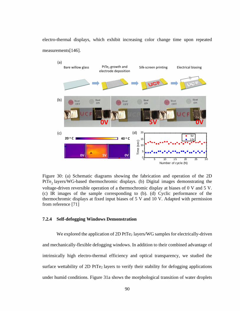
90
electro-thermal displays, which exhibit increasing color change time upon repeated
measurements[146].
Figure 30: (a) Schematic diagrams showing the fabrication and operation of the 2D
PtTe2 layers/WG-based thermochromic displays. (b) Digital images demonstrating the
voltage-driven reversible operation of a thermochromic display at biases of 0 V and 5 V.
(c) IR images of the sample corresponding to (b). (d) Cyclic performance of the
thermochromic displays at fixed input biases of 5 V and 10 V. Adapted with permission
from reference [71]
7.2.4 Self-defogging Windows Demonstration
We explored the application of 2D PtTe2 layers/WG samples for electrically-driven
and mechanically-flexible defogging windows. In addition to their combined advantage of
intrinsically high electro-thermal efficiency and optical transparency, we studied the
surface wettability of 2D PtTe2 layers to verify their stability for defogging applications
under humid conditions. Figure 31a shows the morphological transition of water droplets
0 5 10 15 20 25 300
5
10
15
20
5V
10V
Tim
e (
se
c)
Number of cycle (N)
20 o C 40 o C
0V 5V 0V
Bare willow glass PtTe2 growth and electrode deposition
Silk-screen printing Electrical biasing
(a)
(b)
0V 5V 0V
(c) (d)
91
subsequently integrated on a bare WG (left), after Pt deposition (mid), and its conversion
to 2D PtTe2 layers (right). Interestingly, 2D PtTe2 layers exhibit an extremely large water
contact angle of 108.27°, a significant increase by ∼70° over the bare WG without them
on the surface. The high hydrophobicity of the 2D PtTe2 layers is attributed to their low
polarity arising from the low electronegativity difference between Pt (∼2.28) and Te
(∼2.10) on the Pauling scale[147]. This intrinsically excellent hydrophobicity of 2D
PtTe2 layers suggests implications for self-cleaning surfaces, broadening their versatility
for a wide range of applications. Before investigating the defogging performance of 2D
PtTe2 layers/WG samples, we first examined the mechanical flexibility of a bare WG by
exerting compressive strain. Figure 31b shows its excellent bendability maintaining the
bending radius, R, of ∼1.3 cm. As a control experiment for performance comparison, we
applied a fog of high relative humidity (i.e., 100%) to a bent bare WG without 2D
PtTe2 layers and waited until the fog naturally disappeared at room temperature. We note
that the time required for the complete removal of the fog is >3 min. We then performed
electro-thermal defogging experiments by using large-area (∼5 cm × 2 cm) 2D PtTe2 layers
directly grown on WG substrates prepared with Pt of 1.5 nm thickness. A 2D
PtTe2 layer/WG sample with Au top electrodes maintaining a bending radius of ∼1.3 cm
was mounted on top of a humidifier which produces fog of constant humidity.
Subsequently, the Au electrodes were connected by copper tapes and alligator clips through
which an input voltage of 15 V was applied using a power supply – well below the safe
voltage limit for practical electronic applications. We measured the time span for
electrically-biased defogging once the humidity reached 98% which was set to be time-
zero.

92
Figure 31: (a) Water contact angles of a WG substrate in its pristine state, after the
deposition of 1.5 nm Pt film and growth of 2D PtTe2 layers (left to right). (b) Image of a
WG substrate under compressive strain retaining a bending radius of ∼1.3 cm. (c)
Demonstration of electrically driven defogging in a mechanically-flexible 2D
PtTe2 layer/WG sample. (d) Performance comparison of various state-of-the-art
nanomaterials developed for defogging windows. Adapted with permission from reference
[71]
Figure 31c shows snapshot images of progressive defogging in the mechanically
flexible 2D PtTe2layers/WG samples under 15 V. The underlying UCF logo which was
initially invisible became clearly visible after 25 s reaching original transparency indicating
complete defogging. For comparison, we also tested the defogging efficiency of the sample
without mechanical bending under a lower humidity condition of ∼80% and confirmed a
fast defogging time of ∼7 s.

93
Lastly, we compared the defogging performances of 2D PtTe2 layer-based
windows with those of the other previously explored nanomaterials, as presented in Figure
31d. We note that the 2D PtTe2 layers exhibit the smallest sheet resistance compared to
other state-of-the-art nanomaterials adopted in defogging windows – i.e., ∼10% smaller
than MXenes and ∼35% smaller than single-walled carbon nanotubes[144, 146, 148-
153]. Although MXenes exhibit slightly better defogging performance – a smaller value
for applied voltage (V) × defogging time (s) [144], their thickness is much larger (i.e., >μm)
than that of the 2D PtTe2layers (thickness: <10 nm), employed for defogging in this study.
Moreover, it is worth mentioning that our defogging experiments were carried out under
very high (98%) humidity while humidity conditions for the other materials were not
specified in the literature
7.3 Conclusion
In conclusion, we studied the electro-thermal properties of wafer-scale 2D
PtTe2 layers and explored them for unconventional smart window applications. We directly
grew 2D PtTe2 layers onto glass substrates on a centimeter scale benefiting from their
intrinsically low growth temperature. We confirmed that they exhibit extremely high
electrical conductivity and electro-thermal conversion efficiency coupled with mechanical
flexibility. Demonstrations of thermochromic displays and electrically-operated defogging
windows were made utilizing these properties, suggesting the high potential of 2D
PtTe2 layers for emerging electro-optical applications.

94
CHAPTER 8 SUMMARY AND FUTURE PERSPECTIVES
8.1 Summary
In this dissertation, we have studied explored the intrinsic property advantages of
2D TMDs layers for mechanically reconfigurable electronic devices, making significant
contributions in the areas of manufacturing techniques compatible with conventional back
end of the line processing techniques. In particular, we studied and showed demonstrations
of strain engineering techniques that can be applied to expand the already-exotic properties
of 2D TMDs, diversifying its applicability. These studies prove that 3D geometric
reconfiguration of 2D TMS layers are essential for mechanically reconfigurable devices.
The main conclusions are presented in the following categories:
1. 2D TMDs have intrinsically exotic electrical, mechanical, optical, thermal and
chemical properties that make them promising candidates for futuristic
mechanically reconfigurable electronic devices. Furthermore, the broad range of
electronic properties make them advantageous over graphene and increases the
versatility of applications.
2. Towards realization of large-scale devices based on 2D TMDs, it is important to
have scalable growth techniques to obtain high-quality wafer-scale 2D TMDs and
subsequently develop transfer methods to integrate the as-grown 2D TMDs on a
variety of substrates. To this end, we employed two-step thermal assisted
conversion (TAC) and developed a chemical-free water-based transfer methods and
showed their viability for synthesizing and transferring large-scale 2D TMDs.
95
3. 3D geometric reconfiguration of 2D TMDs extends their mechanical properties,
allowing for increased degree of freedom, while preserving their structural
integrity. Moreover, they introduce strain-tunability of the 2D TMDs, including
their surface, optical and opto-electrical properties. We explored these patterning
techniques including corrugated crumpling, Kirigami patterning and Serpentine
patterning and showed their applicability for different electronic device.
Overall, the dissertation study suggests that 2D TMDs are an important building block for
mechanically reconfigurable electronics that possess potentials beyond the limitations of
conventional bulk materials. Our studies reduce the gap in existing research study and plays
a vital role in further exploration of 2D TMDs and its scalable fabrication techniques to
meet the increasing demand for wearable and flexible electronics in different sectors
including healthcare, energy, brain-like computing, smart windows and flexible electronics
components.
8.2 Future Perspectives
Despite the projected promises, there still remain major challenges that should be
resolved towards realizing the true potential of 2D TMDs for such futuristic and
unconventional applications in the real-world. Form a materials perspective, it still remains
technically challenging to realize mass production of wafer-scale 2D TMDs with electrical
properties comparable to that of small sized flakes (~µm2). In addition to such large-scale
production, it is also important to develop wafer-scale methods for deterministic transfer
the as-produced 2D TMDs layers with atomic-scale morphology control. From a device

96
fabrication perspective, is it important to understand the fundamental structure-property
correlation between mechanical deformation and electrical properties in 2D TMDs layer,
which is imperative for the evaluation of the durability of electronics based on 2D TMD
layers. Furthermore, towards the applicability of 2D TMDs for wearable electronic devices,
long-term systematic studies to clarify the biocompatibility of 2D TMDs. There is the need
for in vivo and in vitro assessments of the toxicity of 2D TMDs from the aspects of their
physiochemical properties such as shape, size, and chemical compositions.

97
APPENDIX: COPYRIGHT PERMISSIONS
Figure 1

98
Figure 2

99
Figure 3

100
Figure 5

101
Figure 6-7
Figure 8-12
102
Figure 13-18
Figure 19-20
103
Figure 21-23
Figure 28-31
104
LIST OF REFERENCES
1. Jayathilaka, W., et al., Significance of Nanomaterials in Wearables: A Review on
Wearable Actuators and Sensors. Advanced Materials, 2019. 31(7): p. e1805921.
2. Huang, S., et al., Flexible electronics: Stretchable electrodes and their future.
Advanced Functional Materials, 2019. 29(6): p. 1805924.
3. Rus, D. and M.T. Tolley, Design, fabrication and control of soft robots. Nature,
2015. 521(7553): p. 467-75.
4. Koo, J.H., et al., Flexible and stretchable smart display: materials, fabrication,
device design, and system integration. Advanced Functional Materials, 2018.
28(35): p. 1801834.
5. Chun, K.-Y., et al., Highly conductive, printable and stretchable composite films
of carbon nanotubes and silver. Nature Nanotechnology, 2010. 5(12): p. 853.
6. Jeong, C.K., et al., A Hyper-Stretchable Elastic-Composite Energy Harvester.
Advanced Materials, 2015. 27(18): p. 2866-2875.
7. Yu, Z., et al., Intrinsically Stretchable Polymer Light-Emitting Devices Using
Carbon Nanotube-Polymer Composite Electrodes. Advanced Materials, 2011.
23(34): p. 3989-3994.
8. Brabec, C., H.-J. Egelhaaf, and M. Salvador, The path to ubiquitous organic
electronics hinges on its stability. Journal of Materials Research, 2018. 33(13): p.
1839-1840.
9. Lee, E.K., et al., Toward Environmentally Robust Organic Electronics:
Approaches and Applications. Advanced Materials, 2017. 29(44): p. 1703638.
10. Yu, K.J., et al., Inorganic semiconducting materials for flexible and stretchable
electronics. NPJ Flexible Electronics, 2017. 1(1): p. 1-14.
11. Kim, D.H., et al., Stretchable, curvilinear electronics based on inorganic
materials. Advanced Materials, 2010. 22(19): p. 2108-2124.
12. Cann, O. These are the top 10 emerging technologies of 2016. 2016; Available
from: https://www.weforum.org/agenda/2016/06/top-10-emerging-technologies-
2016/.
13. Geim, A.K. and K.S. Novoselov, The rise of graphene. Nature Materials, 2007.
6(3): p. 183-191.
14. Tan, C., et al., Recent Advances in Ultrathin Two-Dimensional Nanomaterials.
Chemical Reviews, 2017. 117(9): p. 6225-6331.
15. Tae-Jun, K., et al., Large-area 2D TMD layers for mechanically reconfigurable
electronic devices. Journal of Physics D: Applied Physics, 2020.
16. Singh, V., et al., Graphene based materials: Past, present and future. Progress in
Materials Science, 2011. 56(8): p. 1178-1271.
17. Novoselov, K.S., et al., A roadmap for graphene. Nature, 2012. 490(7419): p.
192-200.
18. Brownson, D.A.C., D.K. Kampouris, and C.E. Banks, Graphene
electrochemistry: fundamental concepts through to prominent applications.
Chemical Society Reviews, 2012. 41(21): p. 6944-6976.

105
19. Novoselov, K.S., et al., Two-dimensional atomic crystals. Proceedings of the
National Academy of Sciences of the United States of America, 2005. 102(30): p.
10451-10453.
20. Lee, C., et al., Measurement of the elastic properties and intrinsic strength of
monolayer graphene. Science, 2008. 321(5887): p. 385-8.
21. Novoselov, K.S., et al., Two-dimensional gas of massless Dirac fermions in
graphene. Nature, 2005. 438(7065): p. 197-200.
22. Schwierz, F., Graphene transistors. Nature Nanotechnology, 2010. 5(7): p. 487-
496.
23. Liao, L., et al., High-<em>κ</em> oxide nanoribbons as gate dielectrics for high
mobility top-gated graphene transistors. Proceedings of the National Academy of
Sciences, 2010. 107(15): p. 6711-6715.
24. Gusynin, V.P. and S.G. Sharapov, Unconventional Integer Quantum Hall Effect
in Graphene. Physical Review Letters, 2005. 95(14): p. 146801.
25. Bhimanapati, G.R., et al., Recent Advances in Two-Dimensional Materials beyond
Graphene. ACS Nano, 2015. 9(12): p. 11509-11539.
26. Park, J., et al., Composition-Tunable Synthesis of Large-Scale Mo1-xWxS2 Alloys
with Enhanced Photoluminescence. ACS Nano, 2018. 12(6): p. 6301-6309.
27. Susarla, S., et al., Quaternary 2D Transition Metal Dichalcogenides (TMDs) with
Tunable Bandgap. Advanced Materials, 2017. 29(35): p. 1702457.
28. Splendiani, A., et al., Emerging Photoluminescence in Monolayer MoS2. Nano
Letters, 2010. 10(4): p. 1271-1275.
29. Chhowalla, M., et al., The chemistry of two-dimensional layered transition metal
dichalcogenide nanosheets. Nature Chemistry, 2013. 5: p. 263.
30. Geim, A.K. and I.V. Grigorieva, Van der Waals heterostructures. Nature, 2013.
499(7459): p. 419-425.
31. Ajayan, P., P. Kim, and K. Banerjee, Two-dimensional van der Waals materials.
Physics Today, 2016. 69(9): p. 38-44.
32. Yang, H., et al., Structural and quantum-state phase transitions in van der Waals
layered materials. Nature Physics, 2017. 13(10): p. 931-937.
33. Lin, Z., et al., Defect engineering of two-dimensional transition metal
dichalcogenides. 2D Materials, 2016. 3(2): p. 022002.
34. Zhao, Y., et al., Extraordinarily Strong Interlayer Interaction in 2D Layered
PtS2. Advanced Materials, 2016. 28(12): p. 2399-2407.
35. Zhao, Y., et al., High-Electron-Mobility and Air-Stable 2D Layered PtSe2 FETs.
Advanced Materials, 2017. 29(5): p. 1604230.
36. Villaos, R.A.B., et al., Thickness dependent electronic properties of Pt
dichalcogenides. npj 2D Materials and Applications, 2019. 3(1): p. 2.
37. Stolyarova, T.A. and E.G. Osadchii, Standard enthalpies of formation of platinum
selenides PtSe2 and PtSe0.8 (Pt5Se4) from elements. Geochemistry International,
2010. 48(1): p. 91-93.
38. Akinwande, D., et al., A review on mechanics and mechanical properties of 2D
materials—Graphene and beyond. Extreme Mechanics Letters, 2017. 13: p. 42-
77.

106
39. Zhan, H., D. Guo, and G. Xie, Two-dimensional layered materials: from
mechanical and coupling properties towards applications in electronics.
Nanoscale, 2019. 11(28): p. 13181-13212.
40. Bertolazzi, S., J. Brivio, and A. Kis, Stretching and Breaking of Ultrathin MoS2.
ACS Nano, 2011. 5(12): p. 9703-9709.
41. Akinwande, D., N. Petrone, and J. Hone, Two-dimensional flexible
nanoelectronics. Nature Communications, 2014. 5: p. 5678.
42. Islam, M.A., et al., Three dimensionally-ordered 2D MoS2 vertical layers
integrated on flexible substrates with stretch-tunable functionality and improved
sensing capability. Nanoscale, 2018. 10(37): p. 17525-17533.
43. Zheng, Z., et al., Flexible, transparent and ultra-broadband photodetector based
on large-area WSe2 film for wearable devices. Nanotechnology, 2016. 27(22): p.
225501.
44. Fiori, G., et al., Electronics based on two-dimensional materials. Nature
Nanotechnology, 2014. 9: p. 768.
45. Elías, A.L., et al., Controlled Synthesis and Transfer of Large-Area WS2 Sheets:
From Single Layer to Few Layers. ACS Nano, 2013. 7(6): p. 5235-5242.
46. Lee, Y.-H., et al., Synthesis and transfer of single-layer transition metal disulfides
on diverse surfaces. Nano Letters, 2013. 13(4): p. 1852-1857.
47. Islam, M.A., et al., Centimeter-Scale 2D van der Waals Vertical Heterostructures
Integrated on Deformable Substrates Enabled by Gold Sacrificial Layer-Assisted
Growth. Nano Letters, 2017. 17(10): p. 6157-6165.
48. Lin, Z., et al., Controllable Growth of Large–Size Crystalline MoS2 and Resist-
Free Transfer Assisted with a Cu Thin Film. Scientific Reports, 2015. 5: p. 18596.
49. Shim, J., et al., Controlled crack propagation for atomic precision handling of
wafer-scale two-dimensional materials. Science, 2018: p. eaat8126.
50. Yang, R., et al., Tuning Optical Signatures of Single- and Few-Layer MoS2 by
Blown-Bubble Bulge Straining up to Fracture. Nano Letters, 2017. 17(8): p.
4568-4575.
51. Park, M., et al., Tactile Sensors: MoS2‐Based Tactile Sensor for Electronic Skin
Applications (Adv. Mater. 13/2016). Advanced Materials, 2016. 28(13): p. 2555-
2555.
52. Okogbue, E., et al., Centimeter-Scale Periodically Corrugated Few-Layer 2D
MoS2 with Tensile Stretch-Driven Tunable Multifunctionalities. ACS Appl Mater
Interfaces, 2018. 10(36): p. 30623-30630.
53. Ko, H. and A. Javey, Smart Actuators and Adhesives for Reconfigurable Matter.
Accounts of Chemical Research, 2017. 50(4): p. 691-702.
54. Chen, P.Y., et al., From Flatland to Spaceland: Higher Dimensional Patterning
with Two‐Dimensional Materials. Advanced Materials, 2017. 29(23): p. 1605096.
55. Rahneshin, V., et al., The coupled straintronic-photothermic effect. Scientific
reports, 2018. 8(1): p. 1-16.
56. Martella, C., et al., Designer Shape Anisotropy on Transition‐Metal‐
Dichalcogenide Nanosheets. Advanced materials, 2018. 30(9): p. 1705615.
57. Choudhary, N., et al., Strain-Driven and Layer-Number-Dependent Crossover of
Growth Mode in van der Waals Heterostructures: 2D/2D Layer-By-Layer

107
Horizontal Epitaxy to 2D/3D Vertical Reorientation. Advanced Materials
Interfaces, 2018. 5(14): p. 1800382.
58. Kong, D., et al., Synthesis of MoS2 and MoSe2 films with vertically aligned
layers. Nano letters, 2013. 13(3): p. 1341-1347.
59. Pan, Z., et al., Wrinkle Engineering: A New Approach to Massive Graphene
Nanoribbon Arrays. Journal of the American Chemical Society, 2011. 133(44): p.
17578-17581.
60. Martella, C., et al., Anisotropic MoS2 Nanosheets Grown on Self‐Organized
Nanopatterned Substrates. Advanced Materials, 2017. 29(19).
61. Song, Z., et al., Kirigami-Based Stretchable Lithium-Ion Batteries. Scientific
Reports, 2015. 5: p. 10988-10997.
62. Hawkes, E., et al., Programmable Matter by Folding. Proceedings of the National
Academy of Sciences, 2010. 107(28): p. 12441-12445.
63. Hanakata, P.Z., et al., Highly Stretchable MoS2 Kirigami. Nanoscale, 2016. 8(1):
p. 458-463.
64. Qi, Z., D.K. Campbell, and H.S. Park, Atomistic Simulations of Tension-Induced
Large Deformation and Stretchability in Graphene Kirigami. Physical Review B,
2014. 90(24): p. 245437-245444.
65. Blees, M.K., et al., Graphene Kirigami. Nature, 2015. 524: p. 204-213.
66. Lin, Y.-C., et al., Wafer-scale MoS2 thin layers prepared by MoO3 sulfurization.
Nanoscale, 2012. 4(20): p. 6637-6641.
67. Liu, K.-K., et al., Growth of Large-Area and Highly Crystalline MoS2 Thin
Layers on Insulating Substrates. Nano Letters, 2012. 12(3): p. 1538-1544.
68. Islam, M.A., et al., Noble metal-coated MoS2 nanofilms with vertically-aligned
2D layers for visible light-driven photocatalytic degradation of emerging water
contaminants. Scientific Reports, 2017. 7(1): p. 14944.
69. Politano, A., et al., Tailoring the Surface Chemical Reactivity of Transition‐Metal
Dichalcogenide PtTe2 Crystals. Advanced Functional Materials, 2018. 28(15): p.
1706504.
70. Yang, S., et al., Environmental stability of 2D anisotropic tellurium containing
nanomaterials: anisotropic to isotropic transition. Nanoscale, 2017. 9(34): p.
12288-12294.
71. Okogbue, E., et al., Wafer-scale 2D PtTe2 layers for high-efficiency mechanically
flexible electro-thermal smart window applications. Nanoscale, 2020. 12(19): p.
10647-10655.
72. Liu, K.-K., et al., Growth of large-area and highly crystalline MoS2 thin layers
on insulating substrates. Nano letters, 2012. 12(3): p. 1538-1544.
73. Gurarslan, A., et al., Surface-Energy-Assisted Perfect Transfer of Centimeter-
Scale Monolayer and Few-Layer MoS2 Films onto Arbitrary Substrates. ACS
Nano, 2014. 8(11): p. 11522-11528.
74. Kim, J.H., et al., Centimeter-scale Green Integration of Layer-by-Layer 2D TMD
vdW Heterostructures on Arbitrary Substrates by Water-Assisted Layer Transfer.
Scientific Reports, 2019. 9(1): p. 1641.

108
75. Lai, S., et al., Water-penetration-assisted mechanical transfer of large-scale
molybdenum disulfide onto arbitrary substrates. RSC advances, 2016. 6(62): p.
57497-57501.
76. Jung, Y., et al., Metal seed layer thickness-induced transition from vertical to
horizontal growth of MoS2 and WS2. Nano Letters, 2014. 14(12): p. 6842-9.
77. Li, H., et al., From bulk to monolayer MoS2: evolution of Raman scattering.
Advanced Functional Materials, 2012. 22(7): p. 1385-1390.
78. Choudhary, N., et al., Centimeter scale patterned growth of vertically stacked few
layer only 2D MoS 2/WS 2 van der Waals heterostructure. Scientific reports,
2016. 6: p. 25456.
79. Castro-Guerrero, C.F., et al., Structure and catalytic properties of hexagonal
molybdenum disulfide nanoplates. Catalysis Science & Technology, 2011. 1(6): p.
1024-1031.
80. Okogbue, E., et al., Centimeter-Scale Periodically Corrugated Few-Layer 2D
MoS2 with Tensile Stretch-Driven Tunable Multifunctionalities. ACS Applied
Materials & Interfaces, 2018. 10(36): p. 30623-30630.
81. Hsiao, H.H., C.H. Chu, and D.P. Tsai, Fundamentals and applications of
metasurfaces. Small Methods, 2017. 1(4): p. 1600064.
82. Li, H., et al., Optoelectronic crystal of artificial atoms in strain-textured
molybdenum disulphide. Nature communications, 2015. 6(1): p. 1-7.
83. Mangu, V.S., et al., Strain engineering, efficient excitonic photoluminescence,
and exciton funnelling in unmodified MoS 2 nanosheets. Nanoscale, 2017. 9(43):
p. 16602-16606.
84. Derjaguin, B.V., V.M. Muller, and Y.P. Toporov, Effect of contact deformations
on the adhesion of particles. Journal of Colloid and interface science, 1975. 53(2):
p. 314-326.
85. Park, M., et al., MoS2‐based tactile sensor for electronic skin applications.
Advanced Materials, 2016. 28(13): p. 2556-2562.
86. Kang, P., et al., Crumpled Graphene Photodetector with Enhanced, Strain‐
Tunable, and Wavelength‐Selective Photoresponsivity. Advanced Materials, 2016.
28(23): p. 4639-4645.
87. Kim, M., et al., A stretchable crumpled graphene photodetector with
plasmonically enhanced photoresponsivity. Nanoscale, 2017. 9(12): p. 4058-4065.
88. Eda, G., et al., Photoluminescence from chemically exfoliated MoS2. Nano letters,
2011. 11(12): p. 5111-5116.
89. Dong, N., et al., Optical limiting and theoretical modelling of layered transition
metal dichalcogenide nanosheets. Scientific reports, 2015. 5: p. 14646.
90. Kozbial, A., et al., Understanding the intrinsic water wettability of molybdenum
disulfide (MoS2). Langmuir, 2015. 31(30): p. 8429-8435.
91. Choi, J., et al., Hierarchical, dual-scale structures of atomically thin MoS2 for
tunable wetting. Nano letters, 2017. 17(3): p. 1756-1761.
92. Ou, J., et al., Superhydrophobic surfaces on light alloy substrates fabricated by a
versatile process and their corrosion protection. ACS applied materials &
interfaces, 2013. 5(8): p. 3101-3107.

109
93. Choudhury, I.A. and S. Shirley, Laser cutting of polymeric materials: an
experimental investigation. Optics & Laser Technology, 2010. 42(3): p. 503-508.
94. Wagner, S., et al., Highly sensitive electromechanical piezoresistive pressure
sensors based on large-area layered PtSe2 films. Nano letters, 2018. 18(6): p.
3738-3745.
95. Islam, M.A., et al., Noble metal-coated MoS(2) nanofilms with vertically-aligned
2D layers for visible light-driven photocatalytic degradation of emerging water
contaminants. Scientific Reports, 2017. 7: p. 14944.
96. Okogbue, E., et al., Multifunctional Two-Dimensional PtSe2-Layer Kirigami
Conductors with 2000% Stretchability and Metallic-to-Semiconducting
Tunability. Nano Letters, 2019. 19(11): p. 7598-7607.
97. Naveau, A., et al., Interactions of aqueous selenium (− II) and (IV) with metallic
sulfide surfaces. Environmental science & technology, 2007. 41(15): p. 5376-
5382.
98. Zeng, L.H., et al., Fast, self‐driven, air‐Stable, and broadband photodetector
based on vertically aligned PtSe2/GaAs heterojunction. Advanced Functional
Materials, 2018. 28(16): p. 1705970.
99. Lin, S., et al., Tunable active edge sites in PtSe2 films towards hydrogen evolution
reaction. Nano Energy, 2017. 42: p. 26-33.
100. Shyu, T.C., et al., A kirigami approach to engineering elasticity in
nanocomposites through patterned defects. Nature Materials, 2015. 14: p. 785.
101. Tang, Y., et al., Programmable Kiri‐Kirigami Metamaterials. Advanced
Materials, 2017. 29(10): p. 1604262.
102. Zheng, W., et al., Kirigami-inspired highly stretchable nanoscale devices using
multidimensional deformation of monolayer MoS2. Chemistry of Materials, 2018.
30(17): p. 6063-6070.
103. Tang, Y., et al., Programmable Kiri-Kirigami Metamaterials. Advanced
Materials, 2017. 29(10): p. 1604262.
104. Wang, Z., et al., Kirigami-patterned highly stretchable conductors from flexible
carbon nanotube-embedded polymer films. Journal of Materials Chemistry C,
2017. 5(34): p. 8714-8722.
105. Ning, X., et al., Assembly of Advanced Materials into 3D Functional Structures
by Methods Inspired by Origami and Kirigami: A Review. Advanced Materials
Interfaces, 2018. 5(13): p. 1800284.
106. Su, T.-Y., et al., Phase-Engineered PtSe2-Layered Films by a Plasma-Assisted
Selenization Process toward All PtSe2-Based Field Effect Transistor to Highly
Sensitive, Flexible, and Wide-Spectrum Photoresponse Photodetectors. Small,
2018. 14(19): p. 1800032.
107. Han, S.S., et al., Horizontal-to-Vertical Transition of 2D Layer Orientation in
Low-Temperature Chemical Vapor Deposition-Grown PtSe2 and Its Influences on
Electrical Properties and Device Applications. ACS Applied Materials &
Interfaces, 2019. 11(14): p. 13598-13607.
108. Blees, M.K., et al., Graphene kirigami. Nature, 2015. 524: p. 204.
109. Pourbaix, M., J. Van Muylder, and N. De Zoubov, Electrochemical properties of
the platinum metals. Platinum Metals Review, 1959. 3(2): p. 47-53.
110
110. Greeley, J., et al., Alloys of platinum and early transition metals as oxygen
reduction electrocatalysts. Nature chemistry, 2009. 1(7): p. 552-556.
111. Geninatti, T., et al., Impedance characterization, degradation, and in vitro
biocompatibility for platinum electrodes on BioMEMS. Biomedical microdevices,
2015. 17(1): p. 1-11.
112. Zhao, Y., et al., High‐electron‐mobility and air‐stable 2D layered PtSe2 FETs.
Advanced Materials, 2017. 29(5): p. 1604230.
113. Fu, L., et al., Highly Organized Epitaxy of Dirac Semimetallic PtTe2 Crystals with
Extrahigh Conductivity and Visible Surface Plasmons at Edges. ACS Nano, 2018.
12(9): p. 9405-9411.
114. Ko, T.-J., et al., Wafer-scale 2D PtTe2 layers-enabled Kirigami heaters with
superior mechanical stretchability and electro-thermal responsiveness. Applied
Materials Today, 2020. 20: p. 100718.
115. Zhang, T.-Y., et al., A super flexible and custom-shaped graphene heater.
Nanoscale, 2017. 9(38): p. 14357-14363.
116. Han, Y. and W.F. Lu, Structural design of wearable electronics suitable for
highly-stretched joint areas. Smart Materials and Structures, 2018. 27(10): p.
105042.
117. Jang, N.-S., et al., Simple approach to high-performance stretchable heaters
based on kirigami patterning of conductive paper for wearable thermotherapy
applications. ACS applied materials & interfaces, 2017. 9(23): p. 19612-19621.
118. Won, P., et al., Stretchable and transparent kirigami conductor of nanowire
percolation network for electronic skin applications. Nano letters, 2019. 19(9): p.
6087-6096.
119. Kabiri Ameri, S., et al., Graphene electronic tattoo sensors. ACS nano, 2017.
11(8): p. 7634-7641.
120. Kireev, D., et al., Multipurpose and Reusable Ultrathin Electronic Tattoos Based
on PtSe2 and PtTe2. ACS Nano, 2021. 15(2): p. 2800-2811.
121. Hurst, J.W., Naming of the waves in the ECG, with a brief account of their
genesis. Circulation, 1998. 98(18): p. 1937-1942.
122. Sadikoglu, F., C. Kavalcioglu, and B. Dagman, Electromyogram (EMG) signal
detection, classification of EMG signals and diagnosis of neuropathy muscle
disease. Procedia computer science, 2017. 120: p. 422-429.
123. Vidal, F., et al., Linking EEG signals, brain functions and mental operations:
Advantages of the Laplacian transformation. International Journal of
Psychophysiology, 2015. 97(3): p. 221-232.
124. Usakli, A.B., et al., On the use of electrooculogram for efficient human computer
interfaces. Computational intelligence and neuroscience, 2010. 2010.
125. Gao, J.F., et al., Automatic removal of eye-movement and blink artifacts from
EEG signals. Brain topography, 2010. 23(1): p. 105-114.
126. Li, J., W.-Y. Wong, and X.-m. Tao, Recent advances in soft functional materials:
preparation, functions and applications. Nanoscale, 2020. 12(3): p. 1281-1306.
127. Hines, L., et al., Soft Actuators for Small-Scale Robotics. Advanced Materials,
2017. 29(13): p. 1603483.
111
128. LeMieux, M.C., et al., Polymeric Nanolayers as Actuators for Ultrasensitive
Thermal Bimorphs. Nano Letters, 2006. 6(4): p. 730-734.
129. Hu, Y., et al., A spongy graphene based bimorph actuator with ultra-large
displacement towards biomimetic application. Nanoscale, 2014. 6(21): p. 12703-
12709.
130. Zeng, Z., et al., Low-voltage and high-performance electrothermal actuator based
on multi-walled carbon nanotube/polymer composites. Carbon, 2015. 84: p. 327-
334.
131. Chen, L., et al., High-performance, low-voltage, and easy-operable bending
actuator based on aligned carbon nanotube/polymer composites. ACS nano,
2011. 5(3): p. 1588-1593.
132. Yoon, D., Y.-W. Son, and H. Cheong, Negative thermal expansion coefficient of
graphene measured by Raman spectroscopy. Nano letters, 2011. 11(8): p. 3227-
3231.
133. Zhu, S.-E., et al., Graphene-based bimorph microactuators. Nano letters, 2011.
11(3): p. 977-981.
134. Xiao, P., et al., Construction of a fish‐like robot based on high performance
graphene/PVDF bimorph actuation materials. Advanced Science, 2016. 3(6): p.
1500438.
135. Polyimide Film Technical Data Sheet. 2011; Available from:
https://catalog.cshyde.com/Asset/Data%20Sheet%2018-
__F%20Dupont%20Kapton®%20HN%20Film.pdf.
136. Shawkat, M.S., et al., Scalable Van der Waals Two-Dimensional PtTe2 Layers
Integrated onto Silicon for Efficient Near-to-Mid Infrared Photodetection. ACS
Applied Materials & Interfaces, 2021.
137. Mary, H. and G.J. Brouhard, Kappa (<em>κ</em>): Analysis of
Curvature in Biological Image Data using B-splines. bioRxiv, 2019: p. 852772.
138. Bi, H., et al., Microscopic bimetallic actuator based on a bilayer of graphene and
graphene oxide. Nanoscale, 2013. 5(19): p. 9123-9128.
139. Seo, D.K., et al., Twistable and bendable actuator: a CNT/polymer sandwich
structure driven by thermal gradient. Nanotechnology, 2012. 23(7): p. 075501.
140. 정원규, 최석문, and 김용준, Large Displacement Polymer Bimorph Actuator for
Out-of-Plane Motion. Journal of Electrical Engineering and Technology, 2006.
1(2): p. 263-267.
141. Li, Q., et al., Large-Strain, Multiform Movements from Designable
Electrothermal Actuators Based on Large Highly Anisotropic Carbon Nanotube
Sheets. ACS Nano, 2015. 9(1): p. 409-418.
142. Hirose, S. and Y. Umetani, The development of soft gripper for the versatile robot
hand. Mechanism and machine theory, 1978. 13(3): p. 351-359.
143. Cao, Y. and J. Dong, High-performance low-voltage soft electrothermal actuator
with directly printed micro-heater. Sensors and Actuators A: Physical, 2019. 297:
p. 111546.
144. Park, T.H., et al., Shape-Adaptable 2D Titanium Carbide (MXene) Heater. ACS
Nano, 2019. 13(6): p. 6835-6844.

112
145. Tan, L., et al., Direct Growth of Ultrafast Transparent Single-Layer Graphene
Defoggers. Small, 2015. 11(15): p. 1840-1846.
146. Sun, J., et al., Direct Chemical Vapor Deposition-Derived Graphene Glasses
Targeting Wide Ranged Applications. Nano Letters, 2015. 15(9): p. 5846-5854.
147. Wang, M., et al., Wafer-Scale Growth of 2D PtTe2 with Layer Orientation
Tunable High Electrical Conductivity and Superior Hydrophobicity. ACS
Applied Materials & Interfaces, 2020.
148. Sui, D., et al., Flexible and Transparent Electrothermal Film Heaters Based on
Graphene Materials. Small, 2011. 7(22): p. 3186-3192.
149. Sun, H., et al., Large-area self-assembled reduced graphene
oxide/electrochemically exfoliated graphene hybrid films for transparent
electrothermal heaters. Applied Surface Science, 2018. 435: p. 809-814.
150. Wang, J., et al., Flexible, transparent, and conductive defrosting glass. Thin Solid
Films, 2014. 556: p. 13-17.
151. Wang, Z., et al., Germanium-Assisted Direct Growth of Graphene on Arbitrary
Dielectric Substrates for Heating Devices. Small, 2017. 13(28): p. 1700929-
1700936.
152. Shobin, L.R. and S. Manivannan, Enhancement of electrothermal performance in
single-walled carbon nanotube transparent heaters by room temperature post
treatment. Solar Energy Materials and Solar Cells, 2018. 174: p. 469-477.
153. Zhou, B., et al., Ultrathin, flexible transparent Joule heater with fast response
time based on single-walled carbon nanotubes/poly(vinyl alcohol) film.
Composites Science and Technology, 2019. 183: p. 107796-107803.