mean global energy consumption, 1998
TRANSCRIPT

ENIC 6/24/06 H. Atwater Caltech
Photovoltaics: Meeting the Terawatt Challenge
Harry AtwaterThomas J. Watson Laboratories of Applied PhysicsCalifornia Institute of Technology
•Photovoltaics in the Context of Energy Supply Need•Limits to Photovoltaic Efficiency•Silicon PV: the Incumbent Technology•Multijunction PV: Path to Ultrahigh Efficiency•3rd Generation PV: Beyond the Schockley-Queisser Limit•Nanostructures in PV

ENIC 6/24/06 H. Atwater Caltech
Acknowledgments
Richard King - SpectrolabChristiana Honsberg – U. DelawareDave Carlson – BP SolarDick Swanson – SunpowerJurgen Werner – U. StuttgartMartha Symko-Davies - NRELMartin Green - UNSWNate Lewis - Caltech
Brendan KayesChristine RichardsonJames ZahlerMelissa GriggsKatsu Tanabe
Provided ideas, slides, inspiration...
Caltech Group:

ENIC 6/24/06 H. Atwater Caltech
Mean Global Energy Consumption, 1998
4.52
2.7 2.96
0.286
1.21
0.2860.828
0
1
2
3
4
5
TW
Oil Coal Biomass NuclearGas Hydro Renew
Total: 12.8 TW U.S.: 3.3 TW (99 Quads)
Nate Lewis

ENIC 6/24/06 H. Atwater Caltech
1990: 12 TW 2050: 28 TW
Total Primary Power vs Year
Marty Hoffert, NYU

ENIC 6/24/06 H. Atwater Caltech
Energy From Renewables, 1998
10-5
0.0001
0.001
0.01
0.1
1
Elect Heat EtOH Wind Solar PVSolar Th.Low T Sol HtHydro Geoth MarineElec Heat EtOH Wind Sol PV SolTh LowT Sol Hydro GeothMarine
TW
Biomass
5E-5
1E-1
2E-3
1E-4
1.6E-3
3E-1
1E-2
7E-5
Nate Lewis

ENIC 6/24/06 H. Atwater Caltech
(in the U.S. in 2002)
1-4 ¢
2.3-5.0 ¢ 6-8 ¢
5-7 ¢
Production Cost of Electricity
0
5
10
15
20
25
Coal Gas Oil Wind Nuclear Solar
Cost
6-7 ¢
25-50 ¢
Cos
t, ¢/
kW- h
r
US DOE

ENIC 6/24/06 H. Atwater Caltech
• Hydroelectric 0.9 TW
• Geothermal (limited by drilling technology)
• Wind 2 TW
• Biomass 5-7 TW (using > 20% of earth land mass)
• Solar 50 – 1500 TW (resource: 1.2x10⁵ W)
Potential of Renewable Energy
Nate Lewis

ENIC 6/24/06 H. Atwater Caltech
PV Land Area Requirements for US Power
3 TW

ENIC 6/24/06 H. Atwater Caltech
Global PV Land Area Requirements
6 Boxes at 3.3 TW Each

ENIC 6/24/06 H. Atwater Caltech
Explosive Growth in PV Manufacturing

ENIC 6/24/06 H. Atwater Caltech
Solar energy:
Cost : $5.42 / W p*
Goal : $1.00 / W p
Photovoltaics Growth
*USA module price index from solarbuzz.com 6/06
1. Increase Efficiency
2. Lower Cost
• Greater than 40% growth per
year for the last 5 years
• Si dominant technology
• Si supply currently limited and
expensive

ENIC 6/24/06 H. Atwater Caltech
Silicon vs. “Nano-solar” Philosophical and Technical Approach
• Disruptive Solar – seek to alter present PV landscap e• Opportunity for TW Energy Supply (otherwise, why do it?)• 10 Year Time Scale (not longer, because c-Si progre ss forbids it)• Ideally, solar technology suitable for electricity and fuel generation
(1 GW) (10 GW)
100000
(100 GW)
~2020$1/W

ENIC 6/24/06 H. Atwater Caltech
The First Practical Solar Cell-1954

ENIC 6/24/06 H. Atwater Caltech
Improvements in Solar Cell EfficienciesE
ffici
ency
(%)
Universityof Maine
Boeing
Boeing
Boeing
BoeingARCO
NREL
Boeing
Euro-CIS
200019951990198519801975
NREL/Spectrolab
NRELNREL
Japan
Energy
Spire
No. CarolinaState University
Multijunction Concentrators
Three-junction (2-terminal, monolithic)
Two-junction (2-terminal, monolithic)
Crystalline Si Cells
Single crystalMulticrystalline
Thick Si Film
Thin Film Technologies
Cu(In,Ga)Se2
CdTe
Amorphous Si:H (stabilized)
Nano-, micro-, poly- Si
Multijunction polycrystalline
Emerging PV
Dye cells
Organic cells(various technologies)
Varian
RCA
Solarex
UNSW
UNSW
ARCO
UNSWUNSW
UNSWSpire Stanford
Westing-house
UNSWGeorgia Tech
Georgia Tech Sharp
AstroPower(small area)
NREL
Spectrolab
NREL
Matsushita
MonosolarKodak
Kodak
AMETEK Photon Energy
UniversitySo. Florida NREL
NRELCu(In,Ga)Se2
14x concentration
NREL
United Solar
United Solar
RCA
RCARCA
RCARCA
RCA
Boeing-Spectrolab
Solarex
12
8
4
0
16
20
24
28
32
36
EPFL
EPFL
Siemens
2005
Groningen
University LinzUniversity
Linz
NREL
40
NREL (inverted, semi-
mismatched)
Sharp ( large area)
NRELKonarka
University Linz
FhG-ISE
Kaneka(2µm on glass)
Univ.Stuttgart
(45µm thin-filmtransfer)
NREL
NRELNREL
(CdTe/CIS)
Best Research-Cell Efficiencies
US DOE
ENIC 6/24/06 H. Atwater Caltech
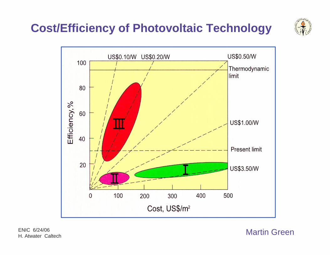
Cost/Efficiency of Photovoltaic Technology
Martin Green

ENIC 6/24/06 H. Atwater Caltech
EC
EV
Eg
np+ p E
Anti-reflection coating
Texturing of front surface
Back surface field}
Rear Contact
h
n
RS
IL RSH
Front Contact
EF
Photovoltaic Solar Cell

ENIC 6/24/06 H. Atwater Caltech
Solar Cell Performance
I I e I I
P V I FF V I
eV k TL
OC L
B= − − == = ⋅
0 01( ) ,/
max max max
saturation current
with illumination
VOC
Vmax
Imax
ISC=IL
Cu
rren
tVoltage
dark
η
λλ
λ
=
=
= ⋅
∞
∫
P P
P A Fhc
d
P FF V I
out in
in
out OC L
/
( )0
where incident power:
power out:
Conversion efficiency:
IL

ENIC 6/24/06 H. Atwater Caltech
Standard Solar Spectra
0
0.5
1
1.5
2
200 400 600 800 1000 1200 1400 1600 1800 2000 2200 2400 2600
Wavelength (nm)
Inte
nsity
per
Uni
t Wav
elen
gth
= S
pect
ral I
rrad
ianc
e (
W/m
2 .
nm)
AM0, ASTM E490-00a, 1366.1 W/m2
AM1.5G, ASTM E892-87, 1000 W/m2
AM1.5D, ASTM G173-03, 1000 W/m2
AM0 – Extraterrestrial solar spectrum
AM1.5G – Global solar spectrum, for flat plate panel s
AM1.5D – Direct solar spectrum, for concentrators
Richard King

ENIC 6/24/06 H. Atwater Caltech
S. M. Sze, Physics of Semiconductor Devices, (Wiley) 1981.
Ec
Ev
Limits to Efficiency: Spectral Absorption
Band-to-BandAbsorption
Subgap PhotonEnergy
Hot CarrierExcitation
Ene
rgy

ENIC 6/24/06 H. Atwater Caltech
Quantum Efficiency Losses
Three types of losses are distinguished:
Base Emitter WindowCourtesy S. Kurtz and D. Friedman
Richard King

ENIC 6/24/06 H. Atwater Caltech
Detailed Balance Limit for Solar Cell Efficiency
absorptionof sunlight
1.511
AM radJN N
q= −
Cell
charge carrierflux
Shockley and Queisser (1961)
radiativeemission
generation rateby sunlightabsorption
radiativerecombinationrate

ENIC 6/24/06 H. Atwater Caltech
• Detailed Balance � “What goes in must come out”
• Balance of energy carriers (not energy):
– Absorbed incident photons from the solar spectrum– Loss of carriers due to radiative recombination
– Extraction of carriers as photocurrent
• Assumptions:
– Perfect absorption of incident photons
– Photo-current loss through radiative reemission:
Detailed Balance Principle And Assumptions
P. Wurfel, Journal of Physics C: Solid State Physics 15, 3967-3985 (1982)
( )
( )
2 2
3 3 2
1
2
sin, , , ,
4
exp 1G
rad cG
E
E
nN E E T V
c
qVd
kT
π θεπ
ωω ω−
=
− − ∫
ℏ
ℏℏ ℏ
( )incident
J V V
Pη
⋅=
Radiative recombination limits cell operating potential to < bandgap potential

ENIC 6/24/06 H. Atwater Caltech
0.0
0.5
1.0
1.5
2.0
0.6 1 1.4 1.8 2.2 2.6 3Bandgap Eg (eV)
Eg/
q, V
oc, a
nd (
Eg/
q) -
Voc
(V
)
0
100
200
300
400
500
600
700
800
Inte
nsity
per
Uni
t Pho
ton
Ene
rgy
(W
/(m
2 . eV
))
VocEg from EQE(Eg/q) - Vocradiative limitAM1.5D, low-AOD
Voc of solar cells with wide range of bandgaps and comparison to radiative limit
d-A
lGaI
nP
GaA
s1.
4 -
eV G
aInA
s
o-G
aInP
AlG
aInA
s
d-A
lGaI
nPd-
GaI
nP
d-A
lGaI
nP
0.97
-eV
GaI
nAs
GaI
nNA
s1.
10-e
V G
aInA
s
1.24
-eV
GaI
nAs
1.30
-eV
GaI
nAs
Ge
(in
dire
ct g
ap)
AlG
aInA
s
Bandgap - Voltage Offset (E g/q) - Voc
for Single-Junction Solar Cells
Richard King

ENIC 6/24/06 H. Atwater Caltech
Detailed Balance:Maximum Cell Efficiency Including Carrier Multiplic ation
Werner, Kolodinski, and Queisser (1994)

ENIC 6/24/06 H. Atwater Caltech
Detailed Balance in Multijunction Solar Cells
Detailed Balance of First Subcell
1.511
AM radJN N
q= −
Cell 1
Cell 2
1.5
1
AM rad radnn n
JN N N
q −= + −Cell n
Cell n+1
Cell n-1
Detailed Balance of n th Subcell

ENIC 6/24/06 H. Atwater Caltech
Maximum Solar Cell EfficienciesTheoretical
95% Carnot eff. = 1 – T/T sun T = 300 K, Tsun ≈≈≈≈5800 K
93% Max. eff. of solar energy conversion = 1 – TS/E = 1 – (4/3)T/Tsun (Henry)
72% Ideal 36-gap solar cell at 1000 suns (Henry)
56% Ideal 3-gap solar cell at 1000 suns (Henry)
50% Ideal 2-gap solar cell at 1000 suns (Henry)
44% Ultimate eff. of device with cutoff E g: (Shockley, Queisser)
43% 1-gap cell at 1 sun with carrier multiplication(>1 e-h pair per photon) (Werner,
Kolodinski, Queisser)
37% Ideal 1-gap solar cell at 1000 suns (Henry)
31% Ideal 1-gap solar cell at 1 sun (Henry )
30% Detailed balance limit of 1 gap solar cell at 1 sun (Shockley, Queisser)
Measured
3-gap GaInP/GaAs/Ge cell @236 suns (Spectrolab)
39.0%
3-gap GaInP/GaAs/Ge cell @ 1 sun (Spectrolab)
32.0%
1-gap solar cell (Si, 1.12 eV) @92 suns (Amonix)
27.6%1-gap solar cell (GaAs, 1.424 eV) @1 sun (Kopin)
25.1%1-gap solar cell (silicon, 1.12 eV) @1 sun (UNSW)
24.7%
ReferencesC. H. Henry, “Limiting efficiencies of ideal single and multiple energy gap terrestrial
solar cells,” J. Appl. Phys., 51, 4494 (1980). W. Shockley and H. J. Queisser, “Detailed Balance Limit of Efficiency of p-n Junction
Solar Cells,” J. Appl. Phys., 32, 510 (1961). J. H. Werner, S. Kolodinski, and H. J. Queisser, “Novel Optimization Principles and
Efficiency Limits for Semiconductor Solar Cells,” Phys. Rev. Lett., 72, 3851 (1994). M. Green, K. Emery, D. L. King, Y. Hisikawa, W. Warta, "Solar Cell Efficiency Tables
(Version 27)", Progress in Photovoltaics, 14, 45 (2006)R. R. King et al., "Pathways to 40%-Efficient Concentrator Photovoltaics," Proc. 20th
European Photovoltaic Solar Energy Conf., Barcelona, Spain, 6-10 June 2005. R. R. King et al., "Lattice-Matched and Metamorphic GaInP/ GaInAs/ Ge Concentrator
Solar Cells," Proc. 3rd World Conf. on Photovoltaic Energy Conversion, May 11-18, 2003, Osaka, Japan, p 622.
A. Slade, V. Garboushian, "27.6%-Efficient Silicon Concentrator Cell for Mass Production," Proc. 15th Int'l. Photovoltaic Science and Engineering Conf., Beijing, China, Oct. 2005.
R. P. Gale et al., "High-Efficiency GaAs/CuInSe2 and AlGaAs/CuInSe2 Thin-Film Tandem Solar Cells," Proc. 21st IEEE Photovoltaic Specialists Conf., Kissimmee, Florida, May 1990.
J. Zhao, A. Wang, M. A. Green, F. Ferrazza, "Novel 19.8%-efficient 'honeycomb' textured multicrystalline and 24.4% monocrystalline silicon solar cells," Appl. Phys. Lett., 73, 1991 (1998).
Richard King

ENIC 6/24/06 H. Atwater Caltech
Cost/Efficiency of Photovoltaic Technology
c-Si

ENIC 6/24/06 H. Atwater Caltech
Absorption via Direct and Indirect Interband Transitions

ENIC 6/24/06 H. Atwater Caltech
Light Absorption and Current Collection
np+ p E

ENIC 6/24/06 H. Atwater Caltech
Auger Recombination Limits to Minority Carrier Lifetime
np+ p E

ENIC 6/24/06 H. Atwater Caltech
Deep Level Impurity Recombination Limits to Minority Carrier Lifetime in p-type Si
np+ p E
ENIC 6/24/06 H. Atwater Caltech
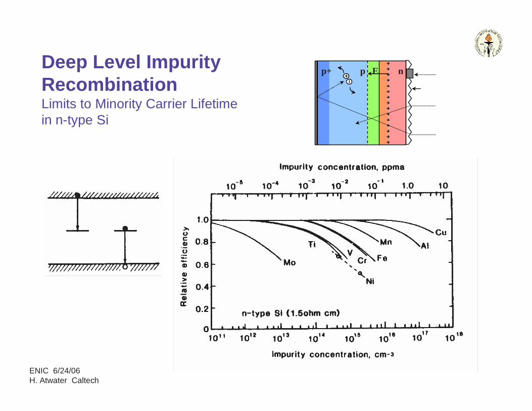
Deep Level Impurity Recombination Limits to Minority Carrier Lifetime in n-type Si
np+ p E

ENIC 6/24/06 H. Atwater Caltech
Open Circuit Voltagelimited by Recombination via a Single Deep Level
[ ( ') ( ')]no po
npR
p p n nτ τ=
+ + +
b
Recombination rate :
exp[ ]qW
( ) ln[ ]
no
L o o oc
b no
L b nooc
o o b
nR
j n p qV
N kT
kT j NV
q qn p W
τ
ττ
=
=
=M.A. Green, High Efficiency Si Solar Cells, Trans Tech, 1987
Under low level injection, p-type Si:
np+ p E

ENIC 6/24/06 H. Atwater Caltech
Factors Limiting Silicon Solar Cell Efficiency
Adapted from R.M. Swanson, Proceedings of the 31st IEEE Meeting (2005) p. 889.
Must work towards lower cost!
ENIC 6/24/06 H. Atwater Caltech
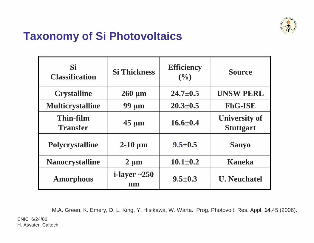
Taxonomy of Si Photovoltaics
U. Neuchatel9.5±0.3i-layer ~250
nmAmorphous
Kaneka10.1±0.22 mNanocrystalline
Sanyo9.5±0.52-10 mPolycrystalline
University of Stuttgart
16.6±0.445 mThin-film Transfer
FhG-ISE20.3±0.599 mMulticrystalline
UNSW PERL24.7±0.5260 mCrystalline
SourceEfficiency
(%)Si Thickness
SiClassification
M.A. Green, K. Emery, D. L. King, Y. Hisikawa, W. Warta. Prog. Photovolt: Res. Appl. 14,45 (2006).

ENIC 6/24/06 H. Atwater Caltech
Cost/Efficiency of Photovoltaic Technology
Thin Films,
Organics

ENIC 6/24/06 H. Atwater Caltech
Thin Film Solar CellsMaterials: CdTe, CuInxGa1-xSe2, poly-Si, amorphous Si
“Inactive”
areasGlass Substrate
p+
n
E
n+
Low Density of UnpassivatedGrain boundaries
Glass Substrate
p+
n
E
n+
High Density of passivatedGrain boundaries

ENIC 6/24/06 H. Atwater Caltech
Poly-Si: Open Circuit Voltage vs. Grain Size
750
grain size g ( m)µ
open
circ
uit v
olta
ge V
(m
V)
oc
700
650
500
550
600
450
400
35010-2 10-1 100 101 102 103
1010
106105
104
Neuchatel
BP
Ti
Astropower Mitsubishi
ETLETLCanon
Tonen
DaidoSanyoKaneka
ASE/ISFH
7S=10 cm/s
ISE
No H passivation during growth
H passivation during growth ‘ideal’ tf-Si
Jurgen Werner

ENIC 6/24/06 H. Atwater Caltech
Cost/Efficiency of Photovoltaic Technology
3J and 4J Cells

ENIC 6/24/06 H. Atwater Caltech
0.5 1.0 1.5 2.00
200
400
600
800
1000
1200
1400
1600
Energy (eV)
Wavelength (µµµµm)
Pow
er (
W m
-2 µµ µµ
m-1)
3.0 2.0 1.01.5
Power Generation Limit in a (GaAs) Single Junction Cell
hνννν ≈ EG hνννν > EG
hνννν < EG
EG
GaAsEG = 1.42 eV
AM1.5

ENIC 6/24/06 H. Atwater Caltech
0.5 1.0 1.5 2.00
200
400
600
800
1000
1200
1400
1600
Energy (eV)
Wavelength (µµµµm)
Pow
er (
W m
-2 µµ µµ
m-1)
3.0 2.0 1.01.5
AM1.5GaInP (1.9 eV)
GaAs (1.4 eV)
Ge (0.7 eV)
Load
Power Generation Limit in a GaInP/GaAs/Ge Triple Junction Cell

ENIC 6/24/06 H. Atwater Caltech
Tunnel Ju
nctio
n
Top Cel
l
Wid
e-Eg T
unnel
Mid
dle Cell
p-GaInP BSF
p-GaInP base
n-Ga(In)As emitter
n+-Ge emitter
p-AlGaInP BSF
n-GaInP emittern-AlInP windown+-Ga(In)As
contact
AR
p-Ge baseand substrate
contact
n-Ga(In)As buffer
Bottom
Cell
p++-TJn++-TJ
p-Ga(In)As base
nucleation
Wide-bandgap tunnel junction
GaInP top cell
Ge bottom cell
n-GaInP window
p++-TJ
n++-TJ
Ga(In)As middle cell
Tunnel junction
Buffer region
Lattice Matched and Metamorphic 3-Junction Cell Cross-Sections
Tunnel Ju
nctio
n
Top Cel
l
Wid
e-Eg T
unnel
Mid
dle Cell
p-GaInP BSF
p-GaInP base
n-GaInAs emitter
n+-Ge emitter
p-AlGaInP BSF
n-GaInP emittern-AlInP windown+-GaInAs
contact
AR
p-Ge baseand substrate
contact
p-GaInAsstep-graded buffer
Bottom
Cell
p++-TJn++-TJ
p-GaInAs base
nucleation
n-GaInP window
p++-TJ
n++-TJ
Lattice-Matched (LM) Lattice-Mismatchedor Metamorphic (MM)
Richard King

ENIC 6/24/06 H. Atwater Caltech
EQE and PL of Subcells Matched to 1%-In and 8%-In GaInAs
0
10
20
30
40
50
60
70
80
90
100
350 450 550 650 750 850 950Wavelength (nm)
Ext
erna
l Qua
ntum
Effi
cien
cy (
%)
0
1500
3000
4500
6000
7500
Pho
tolu
min
esce
nce
Inte
nsity
(a
rb. u
nits
)EQE, lattice-matched
EQE, metamorphic
PL, lattice-matched
PL, metamorphic
1.890 1.813 eV 1.414 1.305 eV
Richard King

ENIC 6/24/06 H. Atwater Caltech
Record Efficiency Solar Cell
• AM1.5 Direct, Low-AOD standard spectrum
• 0.269 cm2
aperture area
• 39.0% record efficiency,236 suns, 25°C
SpectrolabGaInP/ GaInAs/ Ge Cell
Voc = 3.089 V Jsc = 3.377 A/cm2
FF = 88.24%Vmp = 2.749 V
Efficiency = 39.0% ± 2.3%
236 suns (23.6 W/cm2) intensity0.2691 cm2 aperture area25 ± 1°C, AM1.5D, low-AOD spectrum
SpectrolabGaInP/ GaInAs/ Ge Cell
Voc = 3.089 V Jsc = 3.377 A/cm2
FF = 88.24%Vmp = 2.749 V
Efficiency = 39.0% ± 2.3%
236 suns (23.6 W/cm2) intensity0.2691 cm2 aperture area25 ± 1°C, AM1.5D, low-AOD spectrum
Richard King
ENIC 6/24/06 H. Atwater Caltech
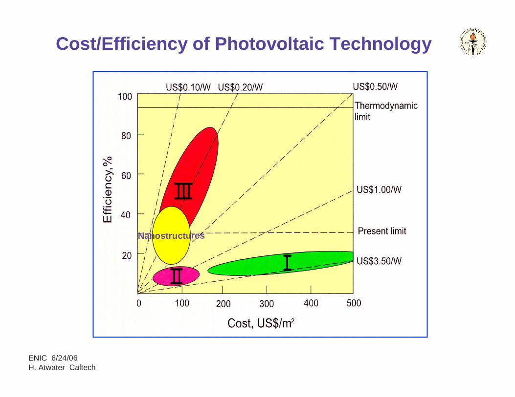
Cost/Efficiency of Photovoltaic Technology
Nanostructures

ENIC 6/24/06 H. Atwater Caltech
Mesocopic Injection Dye-SenstizedSolar Cells
•Electron-hole pairs generated as excitons in a dye absorber (Ru-bpy)
•Excitons diffuse to TiO2interface
•Excitons dissociated into electrons and holes
•Electrons injected in TiO2
•Holes injected into liquid electrolyte
•Potentially low costs for materials and processing
Dye Sensitized Solar Cell
Christiana Honsberg

ENIC 6/24/06 H. Atwater Caltech
Multiple Exciton Generation Solar Cells
•Electron and hole created simultaneously
•Hot electron and hole create multiple (m) electron-hole pairs through Auger emission and absorption instead of thermalizing
•Need materials (e.g., quantum dots) susceptible to creation of multiple Auger electron-hole pairs
•Recently report by NREL and Los Alamos …3 carriers for 1 photon in PbSe
H. Queisser et al., Max Planck Inst.,Solar Energy Materials and Solar Cells, 41/42, 1996
Christiana Honsberg

ENIC 6/24/06 H. Atwater Caltech
Intermediate-Band Solar Cells
• Multiple transition paths via intermediate band
• Theoretical efficiency advantages over equivalent multijunction cells
• Can simplify and augment multijunction solar cell efficiencies
A. Luque et al., U. Politecnica de MadridPhys. Rev. Lett., 78, No. 26, 1997
Band diagram of a solar cell with an intermediate band.
Christiana Honsberg

ENIC 6/24/06 H. Atwater Caltech
Nanowire Photovoltaic Cells
Emergent Concepts for Photovoltaic Nanostructures:
1. Nanowires are a significant opportunity: carrier collection at low diffusion length – ‘improve’ poor quality materials
2. Passivation is essential in nanostructures
3. Multijunction architecture highly desirable for efficiency
4. Sheet Processing : Large-area low-cost reliable processing
0.5 1.0 1.5 2.00
200
400
600
800
1000
1200
1400
1600
Energy (eV)
Wavelength (µµµµm)
Pow
er (
W m
-2 µµ µµ
m-1)
3.0 2.0 1.01.5
AM1.5InGaN (1.8 eV)
Si (1.12 eV)
SiGe (0.8 eV)
Load
InGaN (1.8 eV)
Si (1.12 eV)
SiGe (0.8 eV)
Load

ENIC 6/24/06 H. Atwater Caltech
p-typen-type
Optically thick semiconductor wires
R ≈ Ln
Contact
Radial p-n junction nanowire solar cell
B.M. Kayes, et.al.,J. Appl. Phys. 2005

ENIC 6/24/06 H. Atwater Caltech
R.S. Wagner and W.C. Ellis, Appl. Phys. Lett. 4, 89 -90 (1964)R.S. Wagner and W.C. Ellis, Trans. Metall. Soc. AIM E 233, 1053-1064 (1965)
S.M. Sze Physics of semiconductor devices (New York, Wiley-Interscience, 1969)
Silicon “freezes out”
Photovoltaics may require use of alternative VLS catalysts
Vapor-Liquid-Solid (VLS) Growth
1.12 eV
.27
.54
AuAl
.067
Ga
.16
In
.072

ENIC 6/24/06 H. Atwater Caltech
Vapor-Liquid Solid Synthesis of Si nanowire arrays
In catalyst
Au catalyst

ENIC 6/24/06 H. Atwater Caltech
SiH4
Porous aluminaEvaporated Indium
Wax
Electrodeposited Nickel
After dissolution of the alumina membrane:
VLS nanowire growth in porous alumina templates
In catalyst:

ENIC 6/24/06 H. Atwater Caltech
Multijunction Nanowires
Si Homojunction
0.5 1.0 1.5 2.00
200
400
600
800
1000
1200
1400
1600
Energy (eV)
Wavelength (µµµµm)
Pow
er (
W m
-2 µµ µµ
m-1)
3.0 2.0 1.01.5
hνννν ≈ EG hνννν > EG
hνννν < EG
EG
SiEG = 1.12 eV
AM1.5
0.5 1.0 1.5 2.00
200
400
600
800
1000
1200
1400
1600
Energy (eV)
Wavelength (µµµµm)
Pow
er (
W m
-2 µµ µµ
m-1)
3.0 2.0 1.01.5
AM1.5InGaN (1.8 eV)
Si (1.12 eV)
SiGe (0.8 eV)
Load
InGaN (1.8 eV)
Si (1.12 eV)
SiGe (0.8 eV)
Load
InxGa1-xN/Si/SixGe1-x
Heterojunction

ENIC 6/24/06 H. Atwater Caltech
Multijunction Nanowires
Nanorods are attractive for multijunction PV because:
•Facilitate accommodation of the lattice mismatch between pseudomorphically strained semiconductor materials comprising the heterojunctions structure.
•Force crystallographic defects in strain-relieved dislocated structures to emerge from the rod during growth� single crystal and defect-free rods except near heterojunction interfaces
•Facilitate carrier collection in either axially-oriented or radially-oriented pn junctions.
[100][111]

ENIC 6/24/06 H. Atwater Caltech
Multijunction Nanowires
3 junction heterostructure with 1.85 eV bandgap InxGa1-xN top cell and 0.75 eV GexSi1-x bottom cell; the middle cell is a 1.1 eV Si structure.
InxGa1-xN
Si
InxGa1-xN
SixGe1-x
Si
Single-Crystalline Si/SiGeSuperlattice NanowiresYiying Wu, Rong Fan, and PeidongYang, Nano Lett.; 2002; 2(2) pp 83 - 86;
4.2 4.4 4.6 4.8 5.0 5.2 5.4 5.6 5.8 6.0 6.2 6.4 6.6
Lattice constant (A)
Ene
rgy
Gap
(eV
)
Wav
elen
gth
(µµ µµm
)
01
2
3
4
56
1.02.05.0
0.5
0.3
0.4
0.2
GaAs
PN
Sb
AlN
GaN
InNAlSb
GaPAlAs
InP
InAsGaSb InSb
AlP
As
SiGe

ENIC 6/24/06 H. Atwater Caltech
Summary
•Photovoltaics Resource is TW-capable•Close to Limiting PV Efficiency for Single Junction Cells•Silicon PV is the Incumbent Technology: will it remain so?•Multijunction PV a viable path to >50% •3rd Generation PV: Beyond the Schockley-Queisser Limit•Nanostructures in PV must outperform c-Si by cost/Watt