maximum peak power tracker: a solar application a major
TRANSCRIPT

Maximum Peak Power Tracker:
A Solar Application
A Major Qualifying Project Report
Submitted to the Faculty
Of the
Worcester Polytechnic Institute
In partial fulfillment of the requirements for the
Degree of Bachelor of Science
By
__________________ Daniel F. Butay
__________________
Michael T. Miller
Date: April 24th, 2008
______________________________
Professor Alexander Emanuel, Advisor

2
Acknowledgements
We would like to thank Professor Emanuel for his guidance and patience throughout the
design process of the MQP. His encouragement and insightful contributions made the project
possible. We would also like to thank Professor Bitar for his help with the solar simulator and
input about using solar cells.

3
Abstract
The design and implementation of a Maximum Peak Power Tracking system for a photovoltaic array using boost DC-DC converter topology is proposed. Using a closed-loop microprocessor control system, voltage and current are continuously monitored to determine the instantaneous power. Based on the power level calculated, an output pulse width modulation signal is used to continuously adjust the duty cycle of the converter to extract maximum power. Using a Thevenin power source as well as a solar panel simulator, system design testing confirms simulation of expected results and theoretical operation is obtained.

4
Table of Contents 1.0 Introduction ............................................................................................................................... 6 2.0 Background ................................................................................................................................ 8
2.1 How Solar Cells Work ...................................................................................................... 10
2.2 Solar Cell V-I Characteristic ............................................................................................. 12
2.2.1 Effect of Irradiance ....................................................................................................... 13
2.2.2 Effect of Insolation Levels ............................................................................................. 14
2.2.3 Effect of Temperature .................................................................................................. 16
2.2.3 Efficiency....................................................................................................................... 17
2.3 The DC-DC Boost Converter ............................................................................................ 19
2.3.1 Continuous Conduction Mode ..................................................................................... 20
2.3.2 Boundary between Continuous and Discontinuous Conduction ................................. 22
2.3.3 Discontinuous Conduction Mode ................................................................................. 23
3.0 Methodology ........................................................................................................................... 24 3.1 System Block Diagram ..................................................................................................... 24
3.2 Solar Panel Simulator ...................................................................................................... 25
3.3 Input Filter ....................................................................................................................... 28
3.4 DC-DC Boost Converter Analysis ..................................................................................... 29
3.5 Operating Frequency ....................................................................................................... 31
3.6 Voltage Sensing ............................................................................................................... 31
3.7 Current Sensing ............................................................................................................... 32
3.7.1 Series Sense Resistor .................................................................................................... 32
3.7.2 RDS Sensing .................................................................................................................... 33
3.7.3 Filter Sensing the Inductor ........................................................................................... 34
3.7.4 Magnetic Sensing-Hall Effect Sensors .......................................................................... 36
3.7.5 Current Sensing Conclusion .......................................................................................... 37
3.8 Determining Inductance Value ....................................................................................... 39
3.9 Confirming Peak Power Obtained – Thevenin Equivalence ............................................ 41
3.9.1 Average Current and Ripple ......................................................................................... 43
3.9.3 Equivalent Resistance and Power ................................................................................ 47
4.0 Implementation ....................................................................................................................... 48 4.1 Parts Selection ................................................................................................................ 48
4.1.1 MOSFET Gate Driver Selection ..................................................................................... 48

5
4.1.2 Power Mosfet Selection ............................................................................................... 50
4.1.3 Inductor Selection ........................................................................................................ 54
4.1.4 Diode Selection ............................................................................................................. 57
4.1.5 Voltage Regulator ......................................................................................................... 58
4.1.6 Voltage Sensor .............................................................................................................. 59
4.1.7 Differential Operational Amplifier ................................................................................ 60
4.1.8 Current Sensor .............................................................................................................. 62
4.1.9 Microprocessor Selection ............................................................................................. 63
Pulse Width Modulation (PWM) ........................................................................................... 66
4.2 Controls ........................................................................................................................... 68
Algorithm ............................................................................................................................... 68
5.0 Results ..................................................................................................................................... 71 Theoretical Operation. .......................................................................................................... 76
6.0 Future Recommendations ....................................................................................................... 78 7.0 Conclusion ............................................................................................................................... 80 References ..................................................................................................................................... 82 Full Schematic ................................................................................................................................ 83 Datasheets ..................................................................................................................................... 84
TC4427 MOSFET Driver ......................................................................................................... 84
FDP6030 MOSFET .................................................................................................................. 91
Schottky Diode ...................................................................................................................... 95
LT1121 Voltage Regulator ..................................................................................................... 99
LMC6462 Differential Operational Amplifier ...................................................................... 106
PIC12F683 Microprocessor .................................................................................................. 114
Peak Power Tracking Code .................................................................................................. 116

6
1.0 Introduction
The development of renewable energy has been an increasingly critical topic in the 21st
century with the growing problem of global warming and other environmental issues. With
greater research, alternative renewable sources such as wind, water, geothermal and solar
energy have become increasingly important for electric power generation. Although
photovoltaic cells are certainly nothing new, their use has become more common, practical, and
useful for people worldwide.
The most important aspect of a solar cell is that it generates solar energy directly to
electrical energy through the solar photovoltaic module, made up of silicon cells. Although each
cell outputs a relatively low voltage (approx. 0.7V under open circuit condition), if many are
connected in series, a solar photovoltaic module is formed. In a typical module, there can be up
to 36 solar cells, producing an open circuit voltage of about 20V1. Although the price for such
cells is decreasing, making use of a solar cell module still requires substantial financial
investment. Thus, to make a PV module useful, it is necessary to extract as much energy as
possible from such a system.
A PV module is used efficiently only when it operates at its optimum operating point.
Unfortunately, the performance of any given solar cell depends on several variables. At any
moment the operating point of a PV module depends on varying insolation levels, sun direction,
irradiance, temperature, as well as the load of the system. The amount of power that can be
extracted from a PV array also depends on the operating voltage of that array. As we will
observe, a PV’s maximum power point (MPP) will be specified by its voltage-current (V-I) and
voltage-power (V-P) characteristic curves. Solar cells have relatively low efficiency ratings; thus,
1 Bogus, Klaus and Markvart, Tomas. Solar Electricity. Chichester, New York.Wiley Press, 1994.

7
operating at the MPP is desired because it is at this point that the array will operate at the
highest efficiency. With constantly changing atmospheric conditions and load variables, it is very
difficult to utilize all of the solar energy available without a controlled system. For the best
performance, it becomes necessary to force the system to operate at its optimum power point.
The solution for such a problem is a Maximum Peak Power Tracking system (MPPT).
A MPPT is normally operated with the use of a dc-dc converter (step up or step down).
The DC/DC converter is responsible for transferring maximum power from the solar PV module
to the load. The simplest way of implementing an MPPT is to operate a PV array under constant
voltage and power reference to modify the duty cycle of the dc-dc converter. This will keep
operation constant at or around the maximum peak power point.
There have been many different solutions presented for methods of peak power
tracking. Our goal is to develop such a system with the purpose of obtaining as much energy
from a solar cell as possible. Our secondary goal will be to create such a system that operates
with optimum efficiency as well. Implementing such a design will be useful in the future because
solar cell use is limited greatly by efficiency limitations and cost factors. If manufacturers took
advantage of MPPT systems, it is without a doubt that solar cells will become more commonly
used.
We will focus on a specific solution to the problem of peak power tracking and present it
in full in this report. It will be important to first learn as much as possible about the operation of
solar cells. From there, we will discuss the methodology of the design, the selection of what
components to implement, system design and testing, and finally, the results of our project.
There are a variety of different options and applications available for our goal. The challenge lies

8
in designing a system with maximum efficiency that will quickly and constantly monitor and
change the operation of the system to obtain the optimum performance from a solar cell.
2.0 Background
Most solar cells are made of semiconducting multicrystalline silicon cells, which
currently have efficiencies of 10 to 15%2. Even at these ratings, according to the Encyclopedia of
Energy, it would take solar modules covering an area equivalent to just 0.25% of the global area
under crops and permanent pasture to meet all the world’s primary energy requirements, when
most or all of such area would otherwise be unused land3. It is numbers like these that
demonstrate the importance and potential that solar cells have in becoming one of the most
important sources of energy used around the world. This also demonstrates the problem with
the use and production of solar cells, limited by low efficiency and high costs.
Despite the limitations, market surveys show that solar cell production is growing
rapidly. With the turn of the century, some companies such as Sharp, BP Solar, and Kyocera
have nearly doubled their production values4.
2 LGBG Technology “Towards 20% Efficient Silicon Solar Cells.” 02 Oct 2005. 3 Aldous, Scott. “How Silicon in Solar Cells Works.” How Stuff Works. 02 Oct 2005. 4 Neville, Richard C. Solar Energy Conversion. The Netherlands: Elsevier Science, 1995.

9
Figure 1: World Solar Cell production from 1988-2002 for the three leading production regions and the
rest of the world
Figure 2: World PV market by application from 1990-2001
PV modules are also being applied for a greater variety of different purposes. Although
they have not yet broken into the consumer market, as we can see from figure, the use of PV
modules is clearly becoming more successful. Solar cell array efficiency has always been an
important factor for product selection. However, for most potential users, the capital cost, and
the cost of the resultant electricity are much more useful measures on which to base decisions

10
about buying a solar cell. Thus, solar cells that are less efficient, but cheaper per unit area are
able to compete in the market.
Solar cells are being valued as a source of energy, but they are also favored for their
beneficial effect on the environment. To put this aspect into perspective, consider the carbon
dioxide emissions during the operation of other methods of energy production. For example,
assuming that U.S. energy generation causes 160 g carbon equivalent of CO2 per kilowatt-hour
of electricity, then a 1-kW PV array in an average U.S. location would produce approximately
1600kWh each year and 48,000kWh in 30 years. This array would avoid approximately (48,000 x
0.95) x 160g/kWh, or approximately 7 metric tons of carbon equivalent during its useful life5. A
global implementation of solar cell arrays could very well be the solution to many environmental
problems. The value of PV arrays is irrefutable, and clearly on the rise. The use of efficiency
boosting systems like MPPTs provide a very promising future for solar cell use and the key to
success is in understanding how solar cells work.
2.1 How Solar Cells Work
Solar cells produce energy by performing two basic tasks: (1) absorption of light energy
to create free charge carriers within a material and (2) the separation of the negative and
positive charge carriers in order to produce electric current that flows in one direction across
terminals that have a voltage difference. Solar cells perform these tasks with their
semiconducting materials. The separation function is typically achieved through a p-n junction.
Solar cell regions are made up of materials that have been “doped” with different impurities.
This creates an excess of free electrons (n-type) on one side of the junction, and a lack of free
5 Sayigh, A.A.M., ed. Solar Energy Engineering. New York, USA: Academic Press, 1977.

11
electrons (p-type) on the other. This behavior creates an electrostatic field with moving
electrons and a solar cell is essentially, a large-area diode6.
Figure 3 describes the overall process of solar energy conversion. First, photons enter
the cell throughout the surface of the array. The photon is absorbed and its energy is
transferred to an electron in the semiconductor. This frees the electron from its parent atom,
and leaves behind a positively charged vacancy, otherwise known as a “hole.” The movement of
electrons and holes with the cell responds to the electric field or by diffusion to areas where
electrons are less concentrated. Due to a strong electric field, electron-hole pairs generated
near the junction are split apart. Minority carriers (electrons in p-type material and holes in n-
type), are swept across the junction and become majority carriers. It is this crossing that occurs
by the individual carriers that contributes to the cell’s output current. Finally, metal contacts on
the cell allow connection of the generated current to a load.
.
Figure 3: Solar cell operation
6 Richard Corkish, Solar Cells (Encyclopedia of Energy, 2004)

12
2.2 Solar Cell V-I Characteristic
Each solar cell has its own voltage-current (V-I) characteristic. Figure 4 shows the V-I
characteristic of a typical photovoltaic cell. The problem with extracting the most possible
power from a solar panel is due to nonlinearity of the characteristic curve. The characteristic
shows two curves, one shows the behavior of the current with respect to increasing voltage. The
other curve is the power-voltage curve and is obtained by the equation (P=I*V).
Figure 4: Solar panel V-I characteristic and Power curve
When the P-V curve of the module is observed, one can locate a single maxima of power where
the solar panel operates at its optimum. In other words, there is a peak power that corresponds
to a particular voltage and current. Obtaining this peak power requires that the solar panel
operate at or very near the point where the P-V curve is at the maximum. However, the point
where the panel will operate will change and deviate from the maxima constantly due to

13
changing ambient conditions such as insolation or temperature levels, which we will discuss
further. The result is a need for a system to constantly track the P-V curve to keep the operating
point as close to the maxima as much as possible while energy is extracted from the PV array.
2.2.1 Effect of Irradiance
Solar panels are only as effective as the amount of energy they can produce. Because
solar panels rely on conditions that are never constant, the amount of power extracted from a
PV module can be very inconsistent. Irradiance is an important changing factor for a solar array
performance. It is a characteristic that describes the density of radiation incident on a given
surface. In terms of PV modules, irradiance describes the amount of solar energy that is
absorbed by the array over its area. Irradiance is expressed typically in watts per square meter
(W/m2). Given ideal conditions, a solar panel should obtain an irradiance of 100mW/cm2, or
1000W/ m2)7. Unfortunately, this value that is obtained from a solar panel will vary greatly
depending on geographic location, angle of the sun, or the amount of sun that is blocked from
the panel because of any present clouds or haze. Although artificial lighting can be used to
power a solar panel, PV modules derive most of their energy solely from the energy emitted
from the sun. Therefore, changes of irradiance will greatly affect a PV module’s performance.
7 Richard Corkish, Solar Cells (Encyclopedia of Energy, 2004)

14
Figure 5: Different irradiance levels on a solar panel
Figure 5 shows the effect of irradiance on the output of solar panels. Clearly, a smaller
level of irradiance will result in a reduced output. The change in output current is due to the
reduced flux of the photons that move within a cell, as we have discussed when observing the
operation of a solar cell. We can see that the voltage and open circuit voltage is not substantially
affected due to changing levels of irradiance. In fact, the changes made to voltage due to
irradiance are often seen as trivial and independent of the changing flux of photons.
2.2.2 Effect of Insolation Levels
Insolation is closely related to irradiance and refers to the flux of radiant energy from
the sun. Taken as power per unit area, whose intensity and spectral content varies at the earth’s
surface due to time of day (position of the sun), season cloud cover, and moisture content of the
air among other factors much like irradiance, insolation measures how much sunlight energy is
delivered to a specific surface area over a single day8. Insolation is typically measured as
kilowatt-hours per square meter per day (kWh/(m2*day)) or in the case of photovoltaics, as
8 Aldous, Scott. “How Silicon in Solar Cells Works.” How Stuff Works. 02 Oct 2005.

15
kilowatt hours per year per kilowatt peak rating (kWh/kWp*y). In order to obtain the maximum
amount of energy from a PV module, it should be set up perpendicular with the sun straight
overhead, with no clouds or shade.
Figure 6: Insolation Levels across the United States
Figure 6 shows the typical insolation levels across the continental United States during
winter peak sun hours. Some solar panel manufacturers use this scale rather than the average
annual peak sun hour rating because it ensures that their product will deliver reliable and
continuous power in worst-case conditions. Observing this map, we see values varying from 1.1
to 5.5. This encompasses the average values that can be considered low and high for insolation
levels, respectively.

16
Average Insolation (10 year average) kWh/m2/day
State City Jan Feb Mar Apr May Jun Jul Aug Sep Oct Nov Dec Avg
AZ Phoenix 3.25 4.41 5.17 6.76 7.42 7.7 6.99 6.11 6.02 4.44 3.52 2.75 5.38
MA Boston 1.66 2.5 3.51 4.13 5.11 5.47 5.44 5.05 4.12 2.84 1.74 1.4 3.58
AK Anchorage 0.21 0.76 1.68 3.12 3.98 4.58 4.25 3.16 1.98 0.98 0.37 0.12 2.09
Table 1: Insolation Levels (North America)
This table describes the average insolation levels across North America over 10 years.
Unlike the worst-case values, these vary from well below 1 to up to 8. The table reflects the
difference in levels between areas of very high sunlight, to very low sunlight. The yearly average
for Massachusetts is at about the average across the entire nation with a relatively good
average of 3.58. Alaska is expected to receive much lower insolation levels due to its
geographical location and the shortened length of daytime light received especially during the
winter months. Arizona receives better insolation levels because it is located farther south,
making it closer to the equator and ideal operating equations. The same can be observed for
countries throughout the world. Regions close to the equator will commonly achieve much
higher insolation levels than those farther away from the equator.
2.2.3 Effect of Temperature
A PV module’s temperature has a great effect on its performance. Although the
temperature is not as an important factor as the duration and intensity of sunlight it is very
important to observe that at high temperatures, a PV module’s power output is reduced. The
temperature of a PV module also affects its efficiency. In general, a crystalline silicon PV
module’s efficiency will be reduced about 0.5 percent for every degree C increase in
17
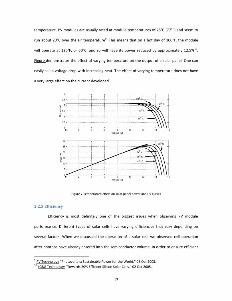
temperature. PV modules are usually rated at module temperatures of 25°C (77°F) and seem to
run about 20°C over the air temperature9. This means that on a hot day of 100°F, the module
will operate at 120°F, or 50°C, and so will have its power reduced by approximately 12.5%10.
Figure demonstrates the effect of varying temperature on the output of a solar panel. One can
easily see a voltage drop with increasing heat. The effect of varying temperature does not have
a very large effect on the current developed.
Figure 7:Temperature effect on solar panel power and I-V curves
2.2.3 Efficiency
Efficiency is most definitely one of the biggest issues when observing PV module
performance. Different types of solar cells have varying efficiencies that vary depending on
several factors. When we discussed the operation of a solar cell, we observed cell operation
after photons have already entered into the semiconductor volume. In order to ensure efficient
9 PV Technology “Photovoltaic: Sustainable Power for the World.” 08 Oct 2005. 10 LGBG Technology “Towards 20% Efficient Silicon Solar Cells.” 02 Oct 2005.

18
absorption, the reflection from the surface of a solar cell must first be reduced. A semiconductor
surface that has already been polished will still reflect a significant fraction of incident photons
from the sun. Silicon, for example, will reflect 30% of such photons11. Texturing the surface of
such cells helps mitigate reflection problems, but the solar panel’s efficiency is defined by other
factors as well.
A solar panel’s efficiency is limited by the bandgap energy of the semiconductor from
which a cell is made. Low bandgap materials will allow the threshold energy to be exceeded by a
large fraction of the photons in sunlight, allowing a potentially high current. On the other hand,
a solar cell will extract from each photon only an amount of energy slightly smaller than the
bandgap energy, with the rest being lost as heat. This is because the excess energy from the
photon results in the electron energy being higher than the bandgap. This leads to the electron
settling in the conduction band and releasing energy as heat. Unfortunately, a semiconductor is
transparent to photons with energy less than that of its bandgap and thus cannot capture their
energy. In other words, the photons do not contain enough energy to create an electron-hole
pair, so the photon simply passes right through the semiconductor. These two factors,
thermalization, and transparency, are two of the largest loss mechanisms in conventional cells12.
As useful as solar panels can be, it is clear that there are still many problems that affect
the overall performance of such an array. This is what contributes to the practicality of the
design. If there was a way to ensure the maximum power is constantly taken from a solar panel
array, a solar panel’s efficiency would increase and the overall usefulness of solar power as a
renewable energy source will be invaluable.
11 Nation Center for Photovoltaics. “Turning Sunlight into Electricity.” 20 Oct. 2002. 12 Nation Center for Photovoltaics. “Turning Sunlight into Electricity.” 20 Oct. 2002.

19
2.3 The DC-DC Boost Converter
The boost converter will represent one of the most significant portions to the overall
design of the Maximum Peak Power Tracker. Ideally, the maximum power will be taken from the
solar panels. In order to do so, the panels must operate at their optimum power point. The
output of the solar panel will be either shorted or open circuited through the opening or closing
of a switch. In the design, the switch will actually be a MOSFET, which will be controlled by our
digital controller. For better understanding of the converter, we will model the overall design,
with the MOSFET as a simple, ideal switch. The switch will open and close to control the voltage
across the inductor, essentially operating the panels at their optimum power level.
Figure 8: Step-up (Boost) dc-dc converter
Figure 8 shows the basic design of a step-up converter. As the name implies, the output
voltage is always greater than the input voltage. The operation of the converter depends on the
state of the switch. To better understand the operation of the converter, we will examine the
operation of the circuit when the switch is opened or closed while in continuous conduction
mode, discontinuous conduction mode, as well as the boundary between the two modes.
20
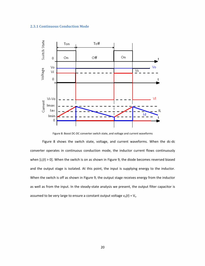
2.3.1 Continuous Conduction Mode
Figure 8: Boost DC-DC converter switch state, and voltage and current waveforms
Figure 8 shows the switch state, voltage, and current waveforms. When the dc-dc
converter operates in continuous conduction mode, the inductor current flows continuously
when [iL(t) > 0]. When the switch is on as shown in Figure 9, the diode becomes reversed biased
and the output stage is isolated. At this point, the input is supplying energy to the inductor.
When the switch is off as shown in Figure 9, the output stage receives energy from the inductor
as well as from the input. In the steady-state analysis we present, the output filter capacitor is
assumed to be very large to ensure a constant output voltage vo(t) = Vo

21
(a) (b)
Figure 9: Boost converter switch on (a), and switch off, (b)
In steady state, the time integral of the inductor voltage over one time period must be zero.
Thus:
Vdton + (Vd – Vo)toff = 0
Dividing both sides by the switching time, Ts, and rearranging terms, we obtain the equation
that describes the relationship between the input and output voltages, switching time, and duty
cycle.
)1(
1
DToff
Ts
Vd
Vo
This equation confirms that the output voltage is always higher than the input voltage. Assuming
a lossless circuit, Pd = Po, we also have
)1( DI
I
d
o

22
2.3.2 Boundary between Continuous and Discontinuous Conduction
At the boundary between continuous and discontinuous conduction, iL goes to zero at
the end of the off interval by definition. At this boundary, the average value of the inductor
current is
In a step-up converter, it is important to recognize that the inductor current and the input
current are the same (id = iL) and using the equation we can find that the average output current
at the boundary of continuous conduction is
2)1(2
DDL
VTI os
oB
The output current reaches its maximum when the duty ratio D = 1/3 = 0.333:
When operating, the average output current at the edge of continuous conduction is important
because for a given D, with constant Vo, if the average load current drops below IOB, the current
conduction would become discontinuous.

23
2.3.3 Discontinuous Conduction Mode
Operation at discontinuous conduction mode cannot be fully understood without
making several assumptions. In practice, the duty cycle, D, would vary with time in order to keep
VO constant. It is this common practice that allows the tracking of the peak power point. In
discontinuous conduction mode, on the other hand, we must assume that as the output load
power decreases, Vd and D remain constant.
Discontinuous conduction mode is unwanted because it occurs due to a decrease in
power and results in a lower inductor current IL since Vd is constant. We will not focus on this
operation mode for the dc-dc converter because hopefully it will be completely avoided.
Nevertheless, it is important to understand the relationship between the input voltage Vd, the
output voltage Vo, and the duty cycle, D. Since in practice Vo is held constant and D varies in
response to the variation in Vd, it is more useful to obtain the required duty ratio as a function of
load current for various values of the ratio Vo/Vd.
24
3.0 Methodology
3.1 System Block Diagram
Solar CellBoost DC-DC
Converter
VI Sensing
Modules
Electric Load or
Battery
PIC
Microprocessor
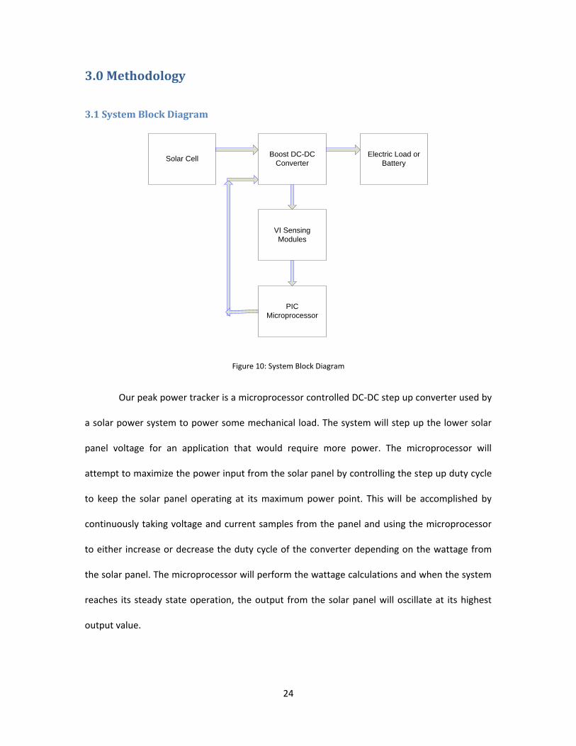
Figure 10: System Block Diagram
Our peak power tracker is a microprocessor controlled DC-DC step up converter used by
a solar power system to power some mechanical load. The system will step up the lower solar
panel voltage for an application that would require more power. The microprocessor will
attempt to maximize the power input from the solar panel by controlling the step up duty cycle
to keep the solar panel operating at its maximum power point. This will be accomplished by
continuously taking voltage and current samples from the panel and using the microprocessor
to either increase or decrease the duty cycle of the converter depending on the wattage from
the solar panel. The microprocessor will perform the wattage calculations and when the system
reaches its steady state operation, the output from the solar panel will oscillate at its highest
output value.

25
3.2 Solar Panel Simulator
In order to provide power to the design, we will be harnessing a solar panel array. The
design will take this power, and operate at the maximum power defined by the panel’s P-V and
I-V characteristics. Rather than using an actual solar panel array to test the design of our PPT, we
will implement a simple solar panel simulator. A solar panel is basically a current source. In
designing a solar panel simulator, our goal was to recreate a solar panel as a current source to
power our circuit. The advantage of using a solar panel simulator is that we can directly control
the output of the solar array, rather than having to deal with the variances that may occur due
to changing operating conditions when testing outdoors. This design also rules out the limitation
of power from artificial lighting sources directed on a solar panel that would have been used
with indoor testing. The following figure is the schematic of the solar panel simulator that will be
used in the testing and design of our PPT.
V112 V
D11N4004GP
D21N4004GP
R1200Ω
0
2
0
R21.5Ω
R31.5Ω
R41.5Ω
R51Ω
0
Output Vsolar
+
_
7
U1
TIP32C
3
1
6
Figure 11:Solar Panel Simulator schematic
26
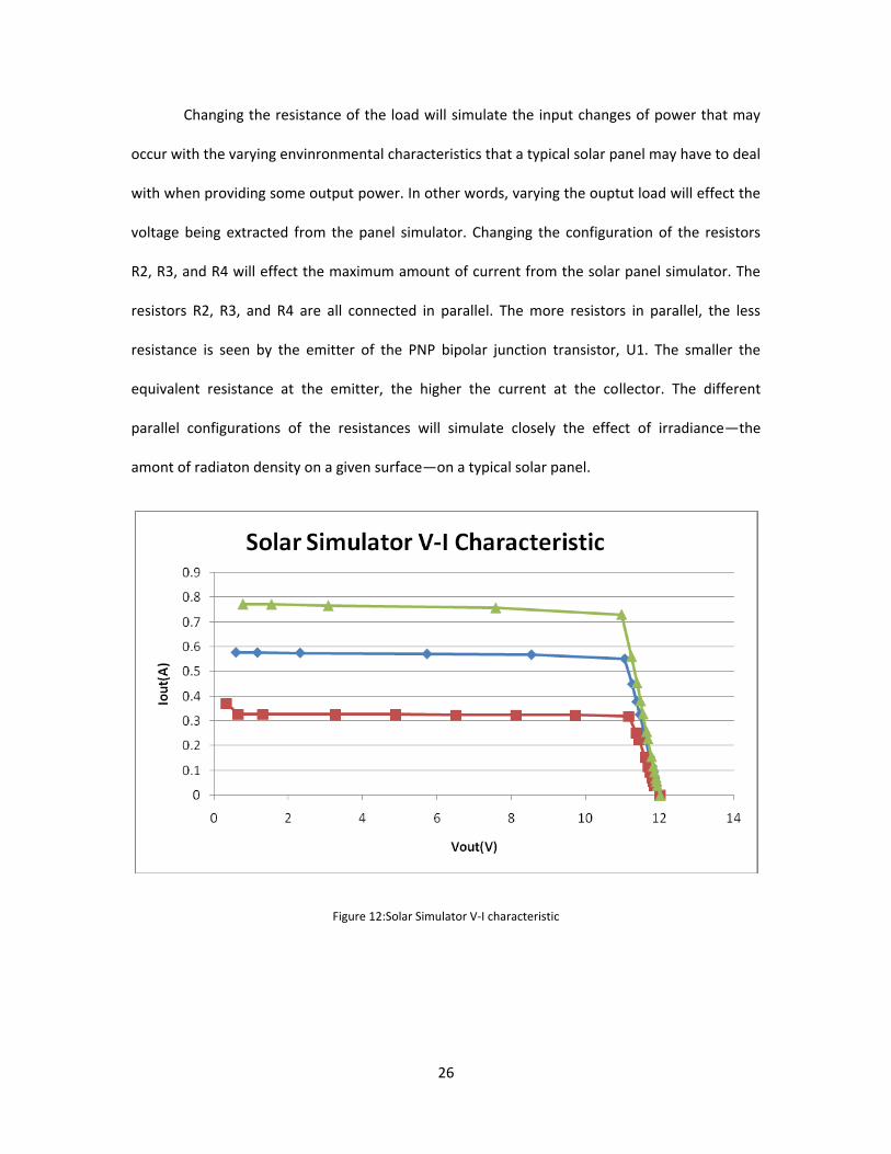
Changing the resistance of the load will simulate the input changes of power that may
occur with the varying envinronmental characteristics that a typical solar panel may have to deal
with when providing some output power. In other words, varying the ouptut load will effect the
voltage being extracted from the panel simulator. Changing the configuration of the resistors
R2, R3, and R4 will effect the maximum amount of current from the solar panel simulator. The
resistors R2, R3, and R4 are all connected in parallel. The more resistors in parallel, the less
resistance is seen by the emitter of the PNP bipolar junction transistor, U1. The smaller the
equivalent resistance at the emitter, the higher the current at the collector. The different
parallel configurations of the resistances will simulate closely the effect of irradiance—the
amont of radiaton density on a given surface—on a typical solar panel.
Figure 12:Solar Simulator V-I characteristic

27
Load(Ω) Vout1(V) Iout1(A)
Vout2(V) Iout2(A) Vout3(V) Iout3(A)
1 0.578 0.578 0.327 0.372 0.772 0.772
2 1.155 0.5775 0.654 0.327 1.541 0.771
4 2.305 0.576 1.309 0.327 3.069 0.766
10 5.721 0.572 3.265 0.326 7.572 0.757
15 8.53 0.569 4.888 0.326 10.958 0.73
20 11.044 0.552 6.505 0.325 11.226 0.561
25 11.249 0.45 8.115 0.325 11.37 0.455
30 11.367 0.379 9.718 0.324 11.467 0.382
35 11.449 0.327 11.151 0.319 11.536 0.329
45 11.56 0.257 11.36 0.252 11.63 0.258
51 11.606 0.227 11.429 0.224 11.669 0.229
75 11.718 0.156 11.59 0.154 11.764 0.157
100 11.779 0.118 11.676 0.117 11.815 0.118
125 11.815 0.0945 11.728 0.0938 11.846 0.0947
169 11.854 0.0701 11.782 0.0697 11.879 0.0703
210 11.875 0.056 11.812 0.0562 11.897 0.0566
300 11.902 0.0397 11.85 0.0395 11.92 0.0397
The figure and respective table shows the V-I characteristic of the solar panel simulator.
These results were experimental, involving the change of load and variable resistors to
determine the outcome. Varying the load resistance resulted in varying levels of output voltage.
Varying the resistance configuration resulted in varying levels of output current. The maximum
output of about 770 mA corresponds to the configuration of all resistances in parallel, while the
output of about 372 mA corresponds to the configuration of just one resistor in series with the
PNP BJT. Vout1 corresponds to two 1.5Ω resistors in parallel, Vout2 corresponds to 3
28
1.5Ωresistors in parallel, while Vout3 corresponds to one 1.5Ω resistor in series with the
transistor. Observing the V-I characteristic, the solar panel simulator’s operation as a typical
solar panel is confirmed, with an open circuit voltage of approximately 11.5V and short circuit
current from 372mA to 770mA depending on the resistance configuration.
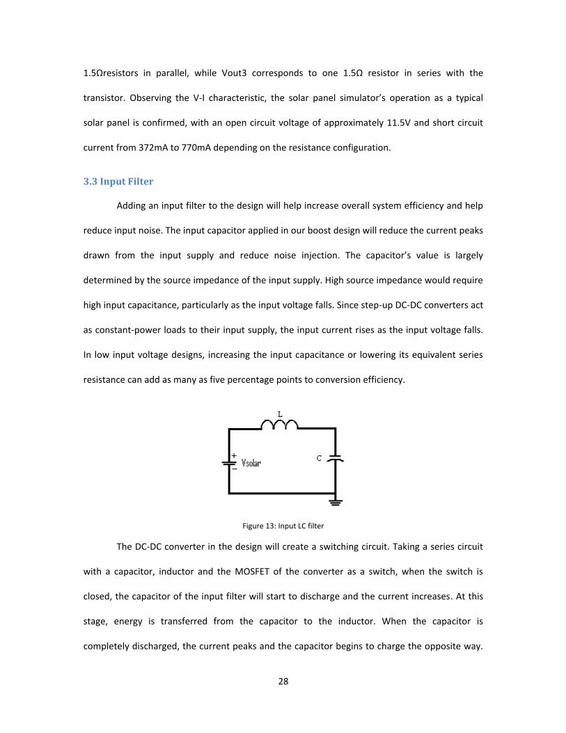
3.3 Input Filter
Adding an input filter to the design will help increase overall system efficiency and help
reduce input noise. The input capacitor applied in our boost design will reduce the current peaks
drawn from the input supply and reduce noise injection. The capacitor’s value is largely
determined by the source impedance of the input supply. High source impedance would require
high input capacitance, particularly as the input voltage falls. Since step-up DC-DC converters act
as constant-power loads to their input supply, the input current rises as the input voltage falls.
In low input voltage designs, increasing the input capacitance or lowering its equivalent series
resistance can add as many as five percentage points to conversion efficiency.
Figure 13: Input LC filter
The DC-DC converter in the design will create a switching circuit. Taking a series circuit
with a capacitor, inductor and the MOSFET of the converter as a switch, when the switch is
closed, the capacitor of the input filter will start to discharge and the current increases. At this
stage, energy is transferred from the capacitor to the inductor. When the capacitor is
completely discharged, the current peaks and the capacitor begins to charge the opposite way.

29
Energy is then transferred back from the inductor to the capacitor. The current alternates
between the inductor and capacitor with an angular frequency in radians/second of
where L is the inductance in henries, and C is the value of capacitance in farads. The LC filter will
be used to decrease the input ripple and improve input efficiency.
3.4 DC-DC Boost Converter Analysis
Figure 14: DC-DC converter simulation circuit
In order to understand and obtain the expected results of the DC-DC converter in the
design, it is important to first simulate operation with the given parameters. The DC-DC
converter is designed with an input voltage of 12V, a boost converter is designed with a 500µH
inductor, 330µF capacitor, an ideal switch and diode, output load of 20Ω. The input pulse signal
to the ideal switch is a 2V pulse with a switching frequency of 100kHz. At a 50% duty cycle, the
converter boosts the input voltage from 12V to the input to 20V at the output. With a simulated
DC-DC boost converter, it was useful to modify the values of the different components of the
circuit as well as the duty cycle in order to obtain the desired results. An input LC filter with a
50µH inductor and 10µF capacitor is also included to observe the effect on the input from
adding a filter to the converter.
30
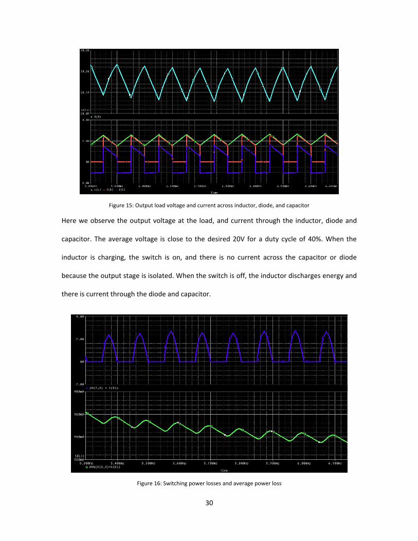
Figure 15: Output load voltage and current across inductor, diode, and capacitor
Here we observe the output voltage at the load, and current through the inductor, diode and
capacitor. The average voltage is close to the desired 20V for a duty cycle of 40%. When the
inductor is charging, the switch is on, and there is no current across the capacitor or diode
because the output stage is isolated. When the switch is off, the inductor discharges energy and
there is current through the diode and capacitor.
Figure 16: Switching power losses and average power loss

31
These two plots describe the losses due to switching. When the switch goes to its off state,
there are power losses due to a loss in energy. The first plot describes a power loss of a little
over 2 watts at each switch. The average power loss is small, less than 1 watt of overall loss for
the system.
3.5 Operating Frequency
The operating frequency of the system will depend on the inductor used and MOSFET
selected. An important factor to consider will be the switching losses associated with the
switching of the circuit. At higher frequencies, the losses due to switching will increase. In
addition, with higher frequencies it is important to keep some resolution in the duty cycle. A
switching frequency of 100kHz was chosen. This switching frequency is appropriate to both the
inductor and the MOSFET chosen. The MOSFET chosen will easily take this as a switching
frequency and resolution is maintained without adding too much in power losses.
3.6 Voltage Sensing
In order for the microprocessor to control the duty cycle of the converter, it needs to
obtain voltage samples from the solar panel input. This will be done through a very simple
method of voltage sensing. Normally, the microprocessor would be able to take voltage directly
from a source to sense the voltage. However, the voltage coming from the solar panel will be
much too large for the microprocessor to handle. The maximum amount of voltage that the
microprocessor will take will be 5V. Any voltage larger than this amount to the microprocessor
would risk destroying it, and the system would fail to monitor and maintain the peak power
operating point all together. Knowing this, it is with great care that we implement the voltage
divider in such a way that it will always output a voltage that is much less than the threshold
voltage of what the microprocessor can handle.

32
Figure 17: Voltage divider
3.7 Current Sensing
To calculate the power coming from the solar panel simulator, the microprocessor
needs to be able to take current samples from the solar panel simulator in addition to the
voltage. In theory, there are several different methods of current sensing. These different
methods vary in their placement within the circuit design and the method of obtaining a current
reading. Because the microprocessor will not be able to take the current from the solar panel
simulator directly, an indirect method of current sensing must be used.
3.7.1 Series Sense Resistor
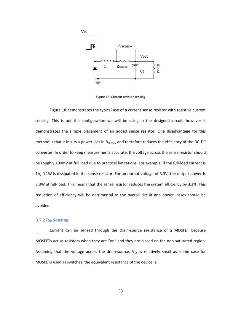
Using a series sense resistor is the conventional way of sensing a current. Resistive
current sensing is done by inserting a resistance into the circuit. The resistance is typically small,
but it used to measure the voltage across the resistor. The voltage seen across the resistor is
proportional to the current, making current sensing possible.
33
Figure 18: Current resistor sensing
Figure 18 demonstrates the typical use of a current sense resistor with resistive current
sensing. This is not the configuration we will be using in the designed circuit, however it
demonstrates the simple placement of an added sense resistor. One disadvantage for this
method is that it incurs a power loss in RSENSE, and therefore reduces the efficiency of the DC-DC
converter. In order to keep measurements accurate, the voltage across the sense resistor should
be roughly 100mV at full load due to practical limitations. For example, if the full-load current is
1A, 0.1W is dissipated in the sense resistor. For an output voltage of 3.3V, the output power is
3.3W at full-load. This means that the sense resistor reduces the system efficiency by 3.3%. This
reduction of efficiency will be detrimental to the overall circuit and power losses should be
avoided.
3.7.2 RDS Sensing
Current can be sensed through the drain-source resistance of a MOSFET because
MOSFETs act as resistors when they are “on” and they are biased on the non-saturated region.
Assuming that the voltage across the drain-source, VDS is relatively small as is the case for
MOSFETs used as switches, the equivalent resistance of the device is:
34
where µ is the mobility, COX is the oxide capacitance, and VT is the threshold voltage. Provided
that RDS is known, the switch current can be determined by sensing the voltage across the drain-
source of the MOSFET.
Figure 19: MOSFET RDS Sensing
The disadvantage to this technique is low accuracy. This is due to the fact that the RDS of
the MOSFET is inherently nonlinear and usually has significant variation because of the mobility,
capacitance and threshold voltage. The RDS is also dependent on the temperature exponentially
which can greatly increase the variation of its actual value. Despite low accuracy, RDS sensing is
useful because it does not add an additional resistance which would result in greater power
losses.
3.7.3 Filter Sensing the Inductor
Instantaneous changes in the input voltage are immediately reflected in the inductor
current, so it is often useful to observe the current across the inductor for current-mode control
in a DC-DC converter. Regardless of the type of feedback control, typically all DC-DC converters
sense the inductor current for over-current protection. Filter sensing the inductor uses a simple

35
low-pass RC network to filter the voltage across the inductor and sense the current through the
equivalent series resistance (ESR) of the inductor.
Figure 20: Filter Sensing the inductor
The voltage across the inductor is given by
where L is the inductor value and RL is the ESR of the inductor. The voltage across the capacitor
of the filter is
where T=L/RL and T1=RFCF. Forcing T=T1 yields VC =RLIL. Because of this relationship, VC is directly
proportional to the current IL. In order to use this technique, L and RL must be known, and then
R and C are chosen accordingly. Because of the tolerance of the components required, this
technique is not appropriate for integrated circuits. The technique is useful for proper design for
a discrete, custom solution where the type and value of the inductor is known.
36
3.7.4 Magnetic Sensing-Hall Effect Sensors
Hall effect sensors sense current by taking advantage of the Hall Effect. According to the
Hall effect, a magnetic field passing through a semiconductor resistor will generate a differential
voltage proportional to the field. Concentric magnetic field lines are generated around a current
carrying conductor. Assuming that the primary current conductor is infinitely long, the magnetic
field strength may be defined as B=µOI/2pr, where µO is the permeability of free space, I is the
current and r is the distance from the center of the current conductor.
To induce a larger signal out of the Hall element the current conductor is wrapped
around slotted ferrous toroid N number of times. This yields the equation for the magnetic field,
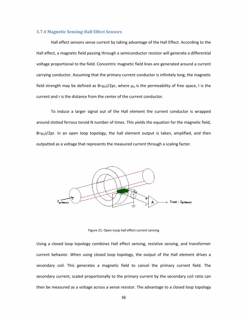
B=µOI/2pr. In an open loop topology, the hall element output is taken, amplified, and then
outputted as a voltage that represents the measured current through a scaling factor.
Figure 21: Open-Loop hall effect current sensing
Using a closed loop topology combines Hall effect sensing, resistive sensing, and transformer
current behavior. When using closed loop topology, the output of the Hall element drives a
secondary coil. This generates a magnetic field to cancel the primary current field. The
secondary current, scaled proportionally to the primary current by the secondary coil ratio can
then be measured as a voltage across a sense resistor. The advantage to a closed loop topology
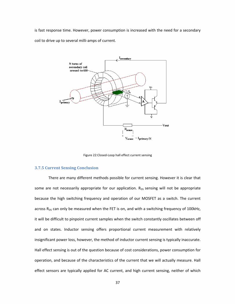
37
is fast response time. However, power consumption is increased with the need for a secondary
coil to drive up to several milli-amps of current.
Figure 22:Closed-Loop hall effect current sensing
3.7.5 Current Sensing Conclusion
There are many different methods possible for current sensing. However it is clear that
some are not necessarily appropriate for our application. RDS sensing will not be appropriate
because the high switching frequency and operation of our MOSFET as a switch. The current
across RDS can only be measured when the FET is on, and with a switching frequency of 100kHz,
it will be difficult to pinpoint current samples when the switch constantly oscillates between off
and on states. Inductor sensing offers proportional current measurement with relatively
insignificant power loss, however, the method of inductor current sensing is typically inaccurate.
Hall effect sensing is out of the question because of cost considerations, power consumption for
operation, and because of the characteristics of the current that we will actually measure. Hall
effect sensors are typically applied for AC current, and high current sensing, neither of which

38
apply to our circuit. In fact, typical Hall effect sensors need to sense at least 5A of current before
they output a differential voltage.
Current Sensing Method Value Accuracy Power Dissipation Relative Cost
Open loop Hall effect sensor - 90-95% Low Medium
Closed loop Hall Effect sensor - >95% Moderate-high High
High Precision Current Sensing
Resistor
.020 >95% Moderate Low
Inductor Filter Sensing - 50% Low Low
RDS Sensing .024 Not applicable Low Low
The method we chose to implement in our circuit is with a high precision current
sensing resistor. This method is the most typically used and the easiest to implement in the
circuit. The method is highly accurate, relatively inexpensive, and has tolerable power
dissipation. The reason why it is defined to have ‘moderate’ power dissipation is because the
power dissipation is relatively insignificant. Inductor filter sensing, for example, relies greatly on
just the equivalent resistance of the inductor, which is typically very small. RDS also has very
small resistance, but the power dissipation is relatively low because no additional resistance is
added to the circuit. The addition of a very small resistance and minimal power loss is the only
disadvantage of using a current sense resistor, and its ease of application more than makes up
for it.

39
Figure 23: Resistive sensing in the boost dc-dc converter
3.8 Determining Inductance Value
In all switching regulator applications, and in our own, the inductor is used as an energy
storage device. When the semiconductor switch is on, the current across the inductor ramps up
and energy is stored within it. When the switch turns off, the energy stored is released into the
load. The inductor’s storage and release of energy in conjunction with the output capacitor is
what accounts for the average output current and voltages resulting in a steady dc output. The
amount of energy stored in an inductor is given by
where L is the inductance in Henrys, and I is the peak value of the inductor current. When
selecting an inductor for a buck converter, as with all switching regulators, the most important
parameters to calculate will be
Maximum input voltage
Output voltage
Switching Frequency
Maximum ripple current
Duty Cycle.

40
For our dc-dc boost converter, if we assume a switching frequency of 100kHz, an input voltage
of 12V, and an output of 20V with a minimum load of 500mA. For an input of 12V, the duty cycle
will be determined by:
This will give us a duty cycle of 0.4 VIN and VO are the input and output voltages respectively. The
voltage across the inductor when on is equal to the input voltage of 12V. When off, the voltage
across the inductor is the difference between VO and VIN, or -8V. The current ripple is given by
the equation:
Choosing a current ripple that is twice that of IIN will allow us to calculate the minimum value of
the inductor what will insure continuous current for a given D, R and switching frequency F. The
current ripple to find the minimum inductance is determined by:
From this simple equation we obtain the minimum inductance:
With VIN = 12V, IIN=0.5A, D=0.4, and fS =100kHz, we obtain the minimum inductance needed for
continuous conduction to be 48µH. With this value obtained, we now know that the inductance
chosen needs to be greater than 48µH otherwise, the dc-dc converter may enter discontinuous
conduction mode and will not operate correctly.

41
Due to the typically high switching frequencies of the controller, inductors with a ferrite
core or equivalent have been recommended, while powdered iron cores are not recommended
due to their high losses at frequencies larger than 50kHz. Once we obtain the peak inductor
current, ILPEAK, we must take care to make sure that the inductor’s saturation rating meets or
exceeds the calculated value for ILPEAK even though most coil types can operate up to 20% over
their saturation rating without experiencing difficulty. In addition, the inductor should have as
low a series resistance as possible. While in continuous operation mode, the power loss in the
inductor resistance, PLR, is approximated by:
where RL is the inductor series resistance.
3.9 Confirming Peak Power Obtained – Thevenin Equivalence
When we design the controller system for the maximum peak power tracker, it is
important to have a full understanding of the boost converter circuit operation. Obtaining the
average current—IAVG, the average voltage, VAVG, the equivalent resistance of the circuit, REQ, the
ripple current, I, and the output power, P—we can predict the outcome of the circuit. To
confirm peak power operation, a Thevenin power source can be used.
The solar panel will be modeled as a linear thevenin voltage and resistance. The goal is
to operate the circuit near the maximum power point of the non-linear I-V characteristic of the
solar panel. Modeling the thevenin power source to have a linear I-V characteristic similar to the

42
solar panel will allow us to monitor the outcome of the circuit to see if peak power is obtained.
Figure 24: Solar panel and thevenin power characteristic comparison
If the maximum power point of the two curves are basically in line, then it will be
beneficial to model the thevenin source. To obtain the correct thevenin voltage and resistance,
simply double the voltage at the maximum power point of the non linear model. This is because
the maximum power point for the linear model will occur at the midpoint and the the thevenin
resistance will simply be the voltage over the current at the maximum power point.
Figure 25: Thevenin power and V-I characteristic
43
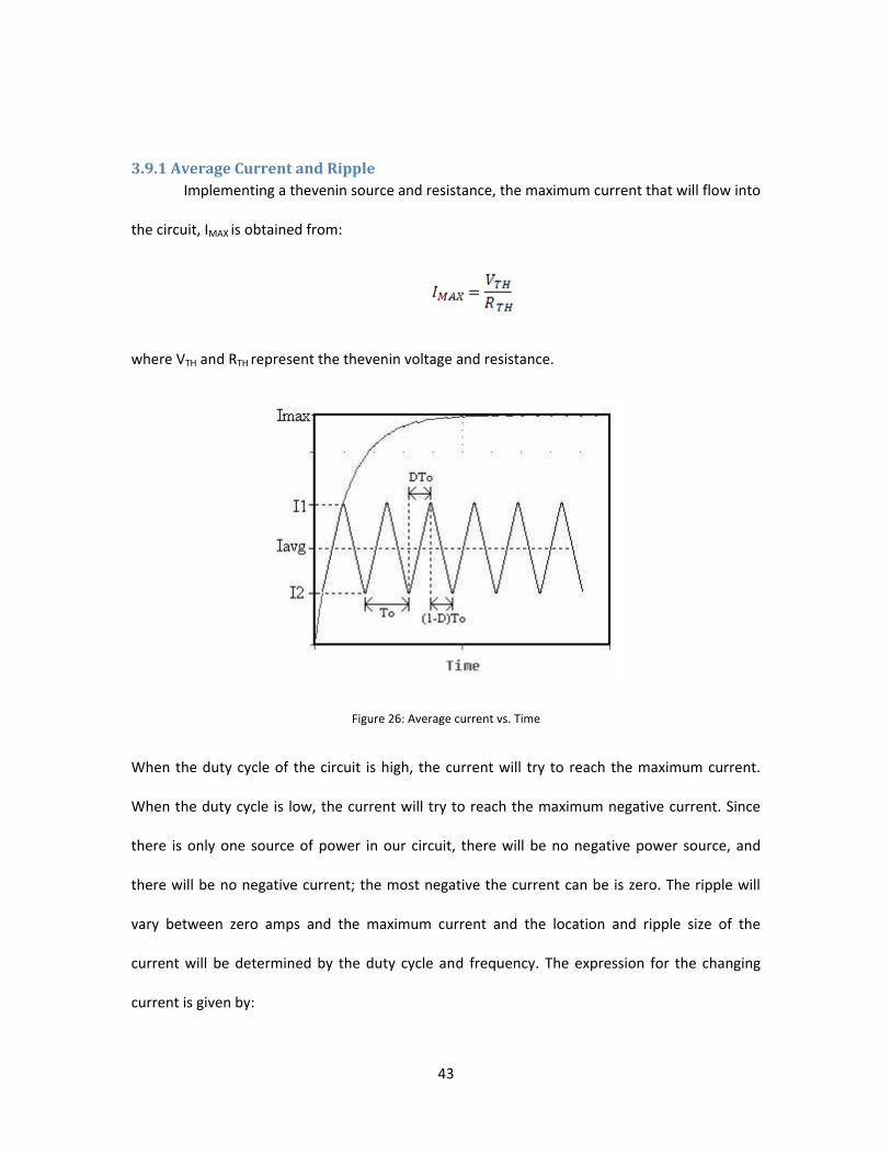
3.9.1 Average Current and Ripple
Implementing a thevenin source and resistance, the maximum current that will flow into
the circuit, IMAX is obtained from:
where VTH and RTH represent the thevenin voltage and resistance.
Figure 26: Average current vs. Time
When the duty cycle of the circuit is high, the current will try to reach the maximum current.
When the duty cycle is low, the current will try to reach the maximum negative current. Since
there is only one source of power in our circuit, there will be no negative power source, and
there will be no negative current; the most negative the current can be is zero. The ripple will
vary between zero amps and the maximum current and the location and ripple size of the
current will be determined by the duty cycle and frequency. The expression for the changing
current is given by:

44
When the duty cycle is high, the initial current, I2 will increase until the duty cycle goes low. This
occurs as I1. The final current will be IMAX, when the duty cycle is high. The time constant L/R is
represented by τ. The time, t, is equivalent to the amount of time in which the duty cycle is high,
DT0, where D is the duty cycle, and T0 is the time period. With T0 much less than the time
constant τ, the equation for I1 is given by
There are now two unknowns, I1 and I2. When the duty cycle is low, the initial current will be at I1
and will drop to I2 while the duty cycle goes high. With no negative current, the relationship
between I2 and I1 is given by
With two equations and two unknowns, we can now solve for the maximum and minimum
ripple values, I1 and I2 as a function of known values: duty cycle, time period, saturation
currents, and τ. To obtain the ripple current, it is necessary to obtain expressions for the ripple
currents that are independent of each other. Using already obtained equations, I1 can be
obtained as
Solving for I1 and simplifying, we obtain

45
To obtain I2, we use the equation
Simplifying, and solving for I2,
Now that we have obtained expressions for I1 and I2, we can now obtain the important value for
IAVG. The average between the two points is simply half of their sum. The average current will be
determined as half the sum of the maximum and minimum ripple values,
Using the previous equations for the ripple values, IAVG can be seen as
With T0 much less than the time constant, τ, any term that depends on either will be
approximately zero, if they affect the result significantly. Keeping this in mind, the simple way of
obtaining the average current is

46
Using this equation, we can observe the effect of the duty cycle on the average current. When
the duty cycle is high, at 100 percent, the average current will go to the maximum positive
saturation value, IMAX. When the duty cycle is low, going to 0, the average current will also go to
0. This makes sense because if the main switch of the MOSFET is always closed, then the current
will try to reach the maximum current, and with the switch constantly closed, the current will
drop to the minimum amount of current, in our case, 0. The current ripple, ΔI, is simply the final
value of the current, I1, minus the initial value I2:
3.9.2 Average Voltage and Ripple
It is now useful to obtain values for the average voltage and the ripple that can be seen
in the voltage. When the main switch is closed for a long period of time, the current will
gradually build through the inductor, and the voltage will drop exponentially at the same rate of
the current increase.
Figure 27: Average voltage vs. time

47
The maximum negative value that the average voltage can be is zero. This is true because when
the current builds to its maximum value, it only depends on the thevenin voltage and resistance,
so the voltage at this point must be zero. When the current is at its minimum, the average
voltage will simply be equivalent to whatever voltage is obtained from the solar panel. Noting
that when the voltage reaches its max, the current reaches its minimum and when the voltage
reaches its maximum, the current goes to its minimum, it will be easy to obtain the expression
for average voltage. This is because the voltage will decrease at the same rate as the current,
but to different points. Thus, the equation for average voltage is very similar to that of the
average current:
With respect to the duty cycle, thevenin voltage and resistance, the inductor, and frequency,
voltage ripple is obtained as
3.9.3 Equivalent Resistance and Power
The average current and voltage have now been obtained. It is now very simple to
derive an expression for the equivalent resistance of the circuit. The equivalent resistance is
obtained simply as the relationship of the average current and average voltage:
The expected average power will also be simple to obtain and also depends on the relationship
between the average voltage and current:

48
When the equivalent resistance of the total circuit equals the Thevenin resistance, maximum
peak power can be observed. This is because the maximum load current is obtained when the
equivalent resistance is twice the total resistance (or when REQ = RTH):
This will be the main method of determining that peak power is obtained. Although we will
observe duty cycle oscillation when peak power is obtained, the method of comparing the
equivalent resistance and thevenin resistance is a dependable way to check to see if the circuit
is acting properly.
4.0 Implementation
4.1 Parts Selection
4.1.1 MOSFET Gate Driver Selection
The MOSFET in our circuit will serve its purpose as a switch. The switching of the FET
according to the defined switching frequency and duty cycle will define the output of the circuit.
After taking voltage and current samples, the microprocessor will output a pulse width
modulated (PWM) signal to modify the duty cycle of the converter. The PWM signal cannot be
connected directly to the MOSFET; instead, we will use a MOSFET driver to pass the signal to the
gate of the MOSFET.
The advantages of using a MOSFET gate driver made it clear that it was the best choice
for implementation. The microprocessor in the circuit can supply only a certain output current.
This limits the ability to charge the FET before it can turn on because the gate of the MOSFET is
capacitive. The gate driver itself will source the current that our MOSFET will draw, and results
49
with a higher current to the FET. With the higher current, the gate driver decreases propagation
delay and allows for a cleaner wave preventing lag in the rise and fall of the FET wave. Another
benefit of using a gate driver is that the it has a higher switching speed than the microprocessor
can achieve, adding to the overall efficiency of the circuit.
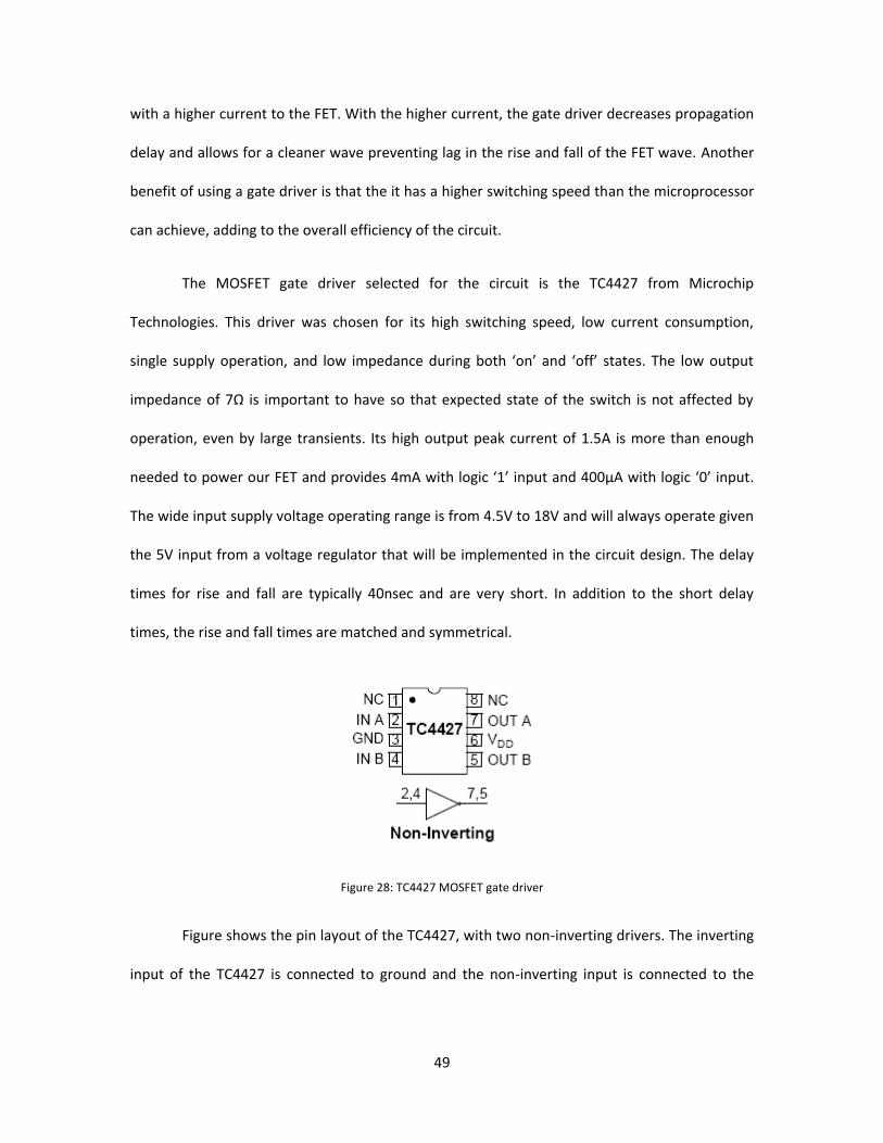
The MOSFET gate driver selected for the circuit is the TC4427 from Microchip
Technologies. This driver was chosen for its high switching speed, low current consumption,
single supply operation, and low impedance during both ‘on’ and ‘off’ states. The low output
impedance of 7Ω is important to have so that expected state of the switch is not affected by
operation, even by large transients. Its high output peak current of 1.5A is more than enough
needed to power our FET and provides 4mA with logic ‘1’ input and 400µA with logic ‘0’ input.
The wide input supply voltage operating range is from 4.5V to 18V and will always operate given
the 5V input from a voltage regulator that will be implemented in the circuit design. The delay
times for rise and fall are typically 40nsec and are very short. In addition to the short delay
times, the rise and fall times are matched and symmetrical.
Figure 28: TC4427 MOSFET gate driver
Figure shows the pin layout of the TC4427, with two non-inverting drivers. The inverting
input of the TC4427 is connected to ground and the non-inverting input is connected to the

50
PWM signal taken from the microprocessor. The output is connected to the gate of the
switching MOSFET of the DC-DC converter.
4.1.2 Power MOSFET Selection
The MOSFET selection is a key factor of the design. The MOSFET in our circuit will act as
the switch that varies the duty cycle of the dc-dc converter, making it possible to step up the
input voltage. A low threshold NFET that specify on-resistance with a gate-source voltage (VGS)
of 2.7V or less is preferred. There are many parameters that must carefully be examined when
choosing a FET. These important constraints include:
1.) Total gate charge (Qg) Predicts switching loss
2.) Reverse transfer capacitance or charge (CRSS) Predicts switching loss
3.) On-resistance (RDS(ON)) Predicts DC losses
4.) Maximum drain-to-source voltage (VDS(MAX))
5.) Minimum threshold voltage (VTH(MIN)).
The most important characteristic to examine will be the FET’s expected power dissipation.
The amount of power that a FET dissipates relies on many constraints. The MOSFET will have
both DC losses and losses due to its constant switching. In order to optimize the efficiency of the
design, it is important to minimize these losses as much as possible. It is also important to
understand that these losses depend on the switching frequency, current, duty cycle, and the
switching rise and fall times. Our goal is to minimize conduction and switching and to choose a
device with sufficient thermal properties. The breakdown voltage, current-carrying capability,
RON, and the RON temperature coefficient will be important parameters to consider.

51
Before a MOSFET begins to switch, the power dissipation derives from conduction losses.
The conduction loss is proportional to the on-state channel resistance, RON of the MOS device
(Q1):
where ID is the drain current, and RON is the channel resistance at the manufacturer’s specified
nominal ambient temperature. The switching losses are contributed by the charging and
discharging of the gate capacitance. To close the FET, a charge from the gate to the source
builds up to allow current to flow. Once the MOSFET’s capacitor achieves a charge equal to its
QG value, the MOSFET switch closes and current flows. When the switch is opened again, the
capacitor discharges all of QG. This loss of charge results in some power loss which increases
with higher switching frequencies:
where VG is the gate-drive voltage, CGS is the gate-source capacitance, and f is the switching
frequency. We can split up the switching losses due to capacitance and switching. The power
loss due to the charging of the capacitor is:
While the power lost due to switching is given by:
Where IRMS is the drain current; tr and tf are the switching rise and fall times, respectively; and VS
is the input source voltage. The total power dissipation in Q1 is given by:

52
.
In this Equation, the first term reflects the conduction loss, while the second term accounts for
the dynamic and gate losses. The dynamic and gate losses are given by the capacitor of the FET
and the losses that occur during switching.
Having calculated the power dissipation, it is also important to calculate the
temperature rise from the thermal resistances of the package. This will be important for the
design once we decide on what heatsink to use (if necessary at all). The temperature rise is as
follows:
Where ΔT is the temperature rise over ambient degrees Celsius, P is the device’s total power
dissipation, and RΘ is the total thermal resistance taken as the sum of junction-to-case
resistance of the FET’s package and the heat-sink thermal resistance. There is also a small case-
to-sink term, however this term is very small and often negligible especially when more modern
thermal interface materials are used.
The MOSFET’s power dissipation is complicated due to its reliance on RON. For example,
a temperature rise of about 80°C causes a 40% increase in the value of RON. To find the actual
temperature rise, we need to include this behavior in the analysis of conduction losses.
Including RON’s temperature coefficient to the power loss equation yields:

53
where δ is the temperature coefficient of RON in ° . Substituting these variables into the
equation for temperature rise, and solving for the device’s ΔT, the temperature rise at the
MOSFET Q1 is given by:
MOSFET Gate Charge QG(nC) Drain-Source
Resistance, RDS (mΩ)
Rise Time, tr (ns) Fall Time, tf (ns)
FDP6030 17 24 20 16
IRL7833 32 3.8 50 6.9
IRFU014 11 200 50 19
IRF7401 48 22 72 92
FDS6880 27 15 18 23
This table lists several comparable power n-channel MOSFETs that would be ideal for
implementation into the circuit. From the data sheets, the most pertinent parameters have
been chosen for power loss analysis, including gate charge, drain-source resistance, and the rise
and fall times typical of switching operation.

54
With switching frequency, f = 100kHz, VS=5V, ID=500mA
MOSFET PC(mW) PQ(mW) PS(mW) Total Loss (mW)
FDP6030 6 8.5 4.5 19.0
IRL7833 0.95 16 7.1125 24.0625
IRFU014 50 5.5 8.625 64.125
IRF7401 5.5 24 20.5 50
FDS6880 3.75 13.5 5.125 22.375
After using the parameters of each FET to calculate the losses due to RDS, the gate
charge, and switching rise and fall times, it is clear that the FDP6030 from Fairchild
Semiconductors is the best choice. The losses taken from each FET increases as frequency
increases, but at our switching frequency of 100kHz, the losses found in the FDP6030 are still
relatively insignificant and is definitely the least among comparable MOSFETs.
4.1.3 Inductor Selection
In an effort to save both money and time, an inductor was tested and designed in the
lab. The advantage was that we were able to make an inductor using readily available material
that did not have to be purchased from a manufacturer. Also, with given design constraints, we
were able to successfully make an inductor with the desired amount of inductance for the
circuit. To create the inductor, an experiment was used that would generate highly consistent
results with those obtained from theoretical predictions employing formulas derived from
Faraday’s law, the Biot-Savart law and Ampere’s law.

55
An inductor serves its most common purpose in circuits to store energy. Inductance
occurs due to a magnetic field that forms around a current-carrying conductor. When an electric
current flows through the conductor, magnetic flux proportional to the current is created. A
change in the current results in a change in the magnetic flux that generates an electromotive
force that acts against the change. Inductance is a measure of the amount of this force (EMF)
generated for each unit change in current. There are many parameters that govern the
inductance of a given inductor—such as the material wrapped around the inductance, the type
of conductor, number of windings or turns, as well as the size of each turn.
An inductor is basically a coil of conducting material, typically copper wire that is
wrapped around some sort of core. Inductors come in many different shapes and sizes; a
circular wire loop, coaxial cable, air-cored solenoid, and ferromagnetic cored toroids are just
some examples. For our purposes, we chose to create a ferromagnetic toroid using a toroid
obtained from the Atwater Kent ECE shop and a length of copper wire. The core chosen was of
ferromagnetic material with a radius, a (from center to the middle of the core) of 20mm, outer
radius, b of 38mm, and height, c of 29mm. The inductance is given by
where µ is the permeability of the core, and N is the number of turns of the wire around the
toroid. However µ is not known initially. A different method of obtaining the inductance is
necessary.
Having created the basic structure of a toroidal inductor, with wire wrapped around a
toroidal core, there were several ways to measure the actual inductance of the toroid. The
inductance of a toroidal core with a circular cross section is given by:
56
where L is the inductance in Henries, µ0 is the permeability of free space = 4π x 10-7 H/m, µr is
the relative permeability of core material, N is the number of turns of the wire, r is the radius of
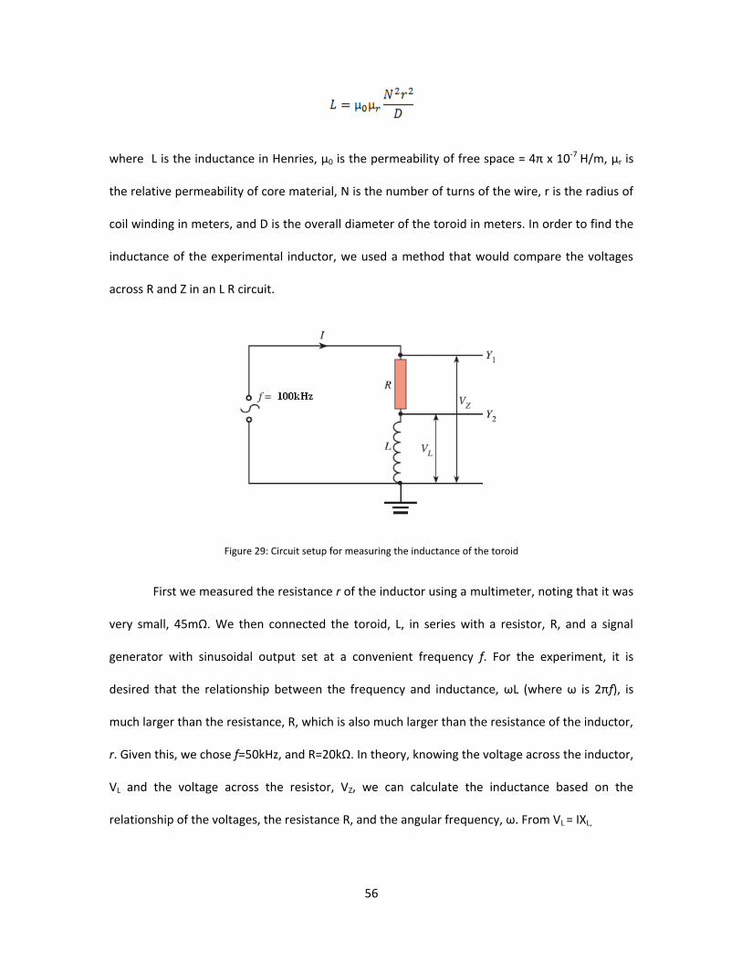
coil winding in meters, and D is the overall diameter of the toroid in meters. In order to find the
inductance of the experimental inductor, we used a method that would compare the voltages
across R and Z in an L R circuit.
Figure 29: Circuit setup for measuring the inductance of the toroid
First we measured the resistance r of the inductor using a multimeter, noting that it was
very small, 45mΩ. We then connected the toroid, L, in series with a resistor, R, and a signal
generator with sinusoidal output set at a convenient frequency f. For the experiment, it is
desired that the relationship between the frequency and inductance, ωL (where ω is 2πf), is
much larger than the resistance, R, which is also much larger than the resistance of the inductor,
r. Given this, we chose f=50kHz, and R=20kΩ. In theory, knowing the voltage across the inductor,
VL and the voltage across the resistor, VZ, we can calculate the inductance based on the
relationship of the voltages, the resistance R, and the angular frequency, ω. From VL = IXL,

57
Using a multimeter, we measure VL =2.2mV, and VZ=0.717mV and ω = 2πf = 2π x 50kHz = 314159
rad/s. With the relationship of the voltages, resistance and frequency, the inductance is given as
Substituting the found values, we obtain L = 498µH, which is very close to the desired results
from simulation of 500µH. Obtaining this value took several attempts as the amount of turns N
of the wire around the toroid had to be changed with each experiment. With a toroidal core
inductor with inductance of 498µH, we were able to use it directly with our circuit by inserting it
as any other type of inductor.
4.1.4 Diode Selection
One of the main goals of the circuit design is to minimize power losses and maximize
efficiency. This goes for basically every part that is implemented in our circuit, including the
diode in our boost DC-DC converter. When boosting the voltage, the diode allows current to
flow to the load while eliminating the possibility of any significant reverse current flowing in the
opposite direction. A reverse current would indicate an unnecessary loss of charge back through
the converter. This is undesirable as it reduces the efficiency of the overall design.
The International Rectifier Schottky Diode was chosen as it was optimized for a very low
forward voltage drop, with moderate leakage. It is typically used with converters and also allows
for reverse battery protection. The diode has a maximum reverse voltage of 60V with a current
rating of 3.3A. The maximum amount of both voltage and current from the solar panel will
always be within this range, and so the diode will perfectly match the constraints of our design.

58
The diode is also labeled to have high frequency operation and high temperature epoxy
encapsulation for enhanced mechanical strength and added safety. With a very low voltage drop
of 0.6V (typ.), the power losses due to the diode are relatively insignificant.
Figure 30: Schottky Diode physical specifications
4.1.5 Voltage Regulator
In order to provide a supply rail of 5 volts to supply the amplifier with a reference
voltage, and to provide power for both the MOSFET driver and PIC microprocessor, a typical
voltage regulator is implemented. The LT1121 voltage regulator was chosen to take the voltage
from the solar panel power supply, and drop it down to a 5-volt supply. The FET driver,
microprocessor and the reference pin of the amplifier will draw much less than the maximum
150mA output of the LT1121. The regulator offers a wide range of input from +/-30V for a
regulated output of 3.3V or 5V. The LT1121 offers adjustable output, however the regulated 5V
will be sufficient for our application. An important feature of the regulator is its ripple rejection.
The circuit that we are designing will have ripple due to constant switching when in operation.
The LT1121 can stabilize any ripple with the addition of external capacitors. The LT1121 specifies

59
stability with only 0.33µF at its input and output. Bypassing either at 1µF will ensure that
stability is always maintained.
Figure 31: LT1121 pin configuration and typical setup
4.1.6 Voltage Sensor
To sense the voltage from the solar panel, we will take the voltage directly from the
power source. The challenge lies in stepping the voltage down from the solar panel, so that the
microprocessor can handle and monitor these values. The microprocessor can handle up to only
5V; anything more will destroy the microprocessor. To be safe, we will allow no more than 3V to
the microprocessor. This can be done simply by implementing a voltage divider. In order to
obtain values for either resistor in the divider, the equation used is:
With the maximum VSOLAR as 12V, and the maximum value for VPIC as 3V, we obtain the relation:
R1 = 3R2. This relation will maintain an input to the microprocessor that will range from zero to 3
volts. We simply chose R2 =3kΩ and R1=1kΩ. These values for the resistors will ensure that no
more than 3V will ever go microprocessor

60
L1
500uH
R1114kΩ
R1210kΩ
Voltage Sampling to PIC
L2
50uH
C210uF
U2FDP6030
D3
10BQ015
C1330uF
R310kΩ
R6
20mΩ
C31uF
4
3
5 21
V112 V
6
0
Figure 32: DC-DC converter with voltage sampling voltage divider
4.1.7 Differential Operational Amplifier
An amplifier is needed in the circuit in order to amplify the voltage signal associated
with the current sample coming from the solar cell. We have seen that the maximum amount of
voltage that the current sense resistor will see will be along the lines of 30mV, although typical
values will be much less—the voltage across the resistor does not reach the order of 30mV until
about 74% duty cycle. To be more accurate when we track and maintain the peak power point,
it is essential that this signal be modified. The current range between 0-30mV will be too small
for the microprocessor to distinguish any viable change in current to output a resulting pwm
signal. The signal must be amplified to at least 1V maximum. The microprocessor will not be
able to take any more than 5V sampling, as we have observed with the voltage divider. In order
to be safe and accurate, it is important that we set the gain of the amplifier accordingly.

61
Figure 33: LMC6462 Operational Amplifier pin setup
The LMC6462 rail-to-rail input and output CMOS operational amplifier is an appropriate
choice for our design specifications. One of the amplifier’s most important qualities is that it
features very low power consumption. The rail-to-rail performance of the amplifier, combined
with its high voltage gain makes it unique among rail-to-rail amps. The system can operate with
a single power source for reference, and does not need a negative power supply, which is not
available in our circuit design.
Figure 34: Operational amplifier gain setting
Like most operational amplifiers, it is relatively simple to set the output gain by
configuring external resistors. To simplify matters, we set the gain for the voltage into the
microprocessor to never exceed 1.2V. Using external resistors and the input voltage, we can set

62
the output voltage to determine the gain necessary. The output from the amplifier is given by
the relation:
The gain, then, is set by the relation between R2 and R1:
With a set gain, we will be able to amplify the current samples to a desired range for the input
of the microprocessor.
4.1.8 Current Sensor
The current sensor of our circuit will consist of the current sense resistor, and the
differential operational amplifier. The current sense resistor will be connected to the solar panel
negative voltage terminal and will connect to the source of the switching MOSFET, connecting it
to ground. The inverting input will be connected to the side of the resistor connected to ground,
while the non-inverting input will be connected to the side that goes to the source of the FET. A
20mΩ current sense resistor is chosen for sensing the current. This resistance was set low
enough to be accurate. If the resistance is too low, then the gain would be forced too high. With
the maximum voltage across the resistor as 30mV, the current through the resistor is :
In order to make sure that there are no over-voltages, it is safe to presume that the maximum
voltage to be sent to the microprocessor is 1.2V. We can obtain the gain needed by dividing the
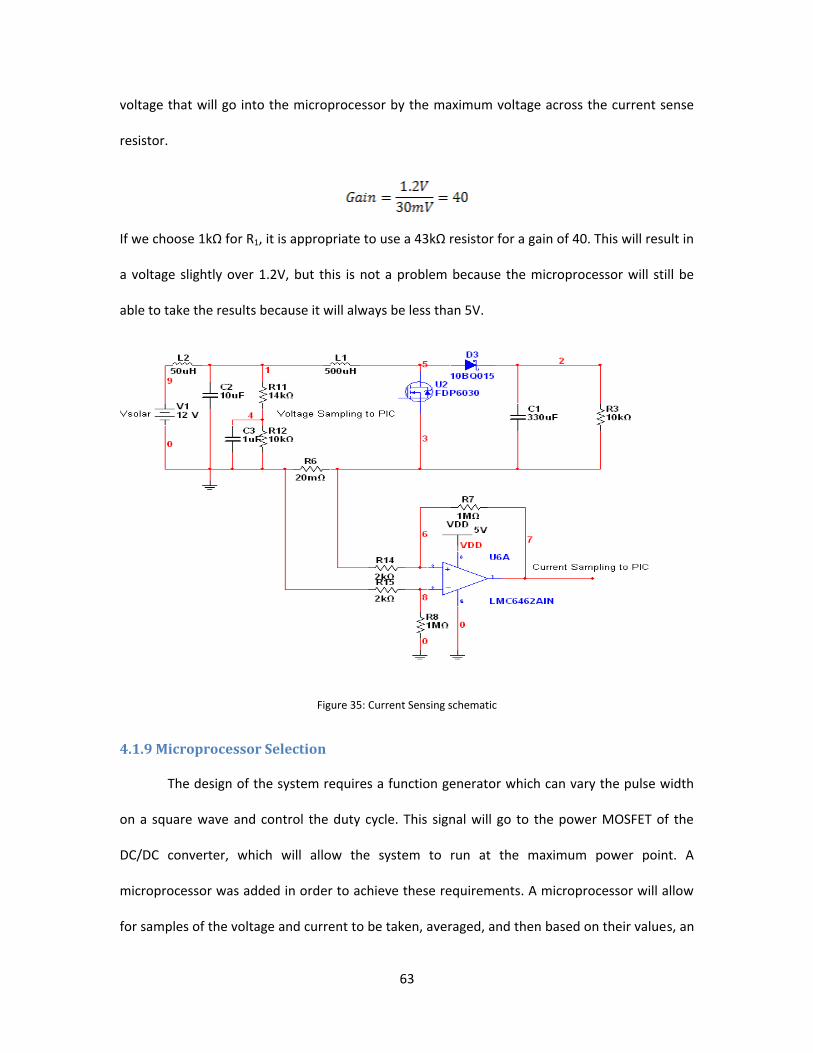
63
voltage that will go into the microprocessor by the maximum voltage across the current sense
resistor.
If we choose 1kΩ for R1, it is appropriate to use a 43kΩ resistor for a gain of 40. This will result in
a voltage slightly over 1.2V, but this is not a problem because the microprocessor will still be
able to take the results because it will always be less than 5V.
Figure 35: Current Sensing schematic
4.1.9 Microprocessor Selection
The design of the system requires a function generator which can vary the pulse width
on a square wave and control the duty cycle. This signal will go to the power MOSFET of the
DC/DC converter, which will allow the system to run at the maximum power point. A
microprocessor was added in order to achieve these requirements. A microprocessor will allow
for samples of the voltage and current to be taken, averaged, and then based on their values, an

64
appropriate signal could be sent out in the form of a PWM signal. The PIC12F683 from microchip
was chosen to accomplish these requirements. It was chosen because of the small size of the
chip, its ability to take in multiple signals and convert them to digital, and its ability to output a
PWM signal with a variable duty cycle.
This is a high performance PIC processor, which only has 8 pins. Five pins are I/O and
one is input only. This allows for a small microprocessor which will not take up much room in
the
design
Figure 36: Pin Diagram of PIC12F683
The microprocessor used needs to be able to work with analog signals that are created
from the system, because of this coexistence it is important to look at the electrical
specifications of the PIC. The maximum voltage from the photovoltaic array will be close to 12V.
The voltage range on pin 1 (VDD) with respect to Vss is -0.3V to 6.5V. Therefore the VDD value
must be reduced before entering the PIC. This is accomplished by the use of a voltage regulator,
explained earlier in the report. The voltage regulator will keep the signal from the Photovoltaic
array at 5V which is in the desired range for the PIC. There is also a maximum current value of
95mA allowed for current into the VDD pin and out of the Vss. These specifications must be met
for the PIC to run successfully. In order to write the code for the PIC12F683 we used MPLAB IDE

65
which is a free software found on the microchip website, www.microchip.com. To program the
PIC the PICSTARTplus was used, which was made available to us in the laboratories at WPI.
Assembly language was chosen because of the low number of instructions needed and with our
familiarity with the language. Analog to Digital Converter
The ADC on the PIC12F683 is internally integrated into the chip. It is a sample and hold
ADC, which will sample the analog signal at a certain sampling frequency and store the digital
representation in two separate registers, one register will hold bits of the value and the other
register will hold a byte of the value. The order that the ten-bit digital representation of the
analog signal is stored can either be right justified or left justified depending on the user’s
preference.
Figure 37: Right and Left Justification of ADC Result
There are a total of four analog input pins; each pin is called a channel. The PIC can only perform
one conversion at a time and the user must specify which channel is to be used before
beginning the conversion process. The conversion takes about 4.67uS to perform, and then the
result can be stored and manipulated by the user. The figure below shows the block diagram of
the ADC.
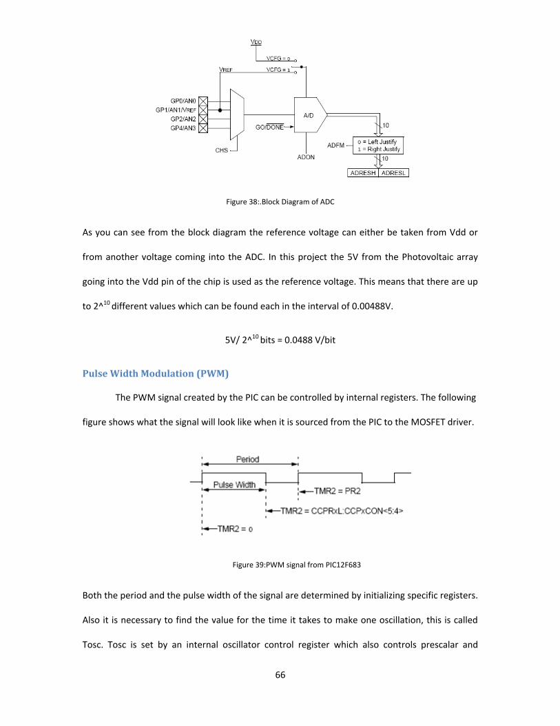
66
Figure 38:.Block Diagram of ADC
As you can see from the block diagram the reference voltage can either be taken from Vdd or
from another voltage coming into the ADC. In this project the 5V from the Photovoltaic array
going into the Vdd pin of the chip is used as the reference voltage. This means that there are up
to 2^10 different values which can be found each in the interval of 0.00488V.
5V/ 2^10 bits = 0.0488 V/bit
Pulse Width Modulation (PWM)
The PWM signal created by the PIC can be controlled by internal registers. The following
figure shows what the signal will look like when it is sourced from the PIC to the MOSFET driver.
Figure 39:PWM signal from PIC12F683
Both the period and the pulse width of the signal are determined by initializing specific registers.
Also it is necessary to find the value for the time it takes to make one oscillation, this is called
Tosc. Tosc is set by an internal oscillator control register which also controls prescalar and

67
postscalar values for the various timers on the PIC, as well as determines whether the oscillator
is set by internal circuitry or external circuitry.
Figure 40. PWM Block Diagram
The block diagram shows the PR2 register and the CCPR1L:CCPR1H registers and how
they will flow into one another, the duty cycle is set by writing to these registers. The signal
outputs from pin CCP1 which is pin 5 on the chip.
Tosc is found from the oscillating frequency (Fosc). It is simply 1/Fosc. The TMR2
Prescale value is set by the TMR2CON register which turns on timer 2 as well as sets a prescale
value which will tell timer 2 what frequency to oscillate at. Register PR2 simply sets a value
between 0-255 which helps determine the period of the PWM signal. The default Fosc is 4MHz,
the prescale value will be set to 1:1, and the register PR2 will be set to 9 making the period
[10*4*(1/4MHz)*1] = 10ms.
The pulse width of the PWM is determined both by the Tosc, and the TMR2 prescale
value but is also determined without the PR2 register. Instead two other registers are used,
CCPR1L and CCP1CON. Both are used for the capture and compare module of the PIC. Together

68
the two CCP registers can store up to 10 bits, which when compared to the PR2 register
multiplied by four amount to the same number.
When the pulse width of the PWM is divided by the period it results in the duty
cycle which is given by the equation below.
This allows for the duty cycle to be anywhere between 0% and 100%.
4.2 Controls
Algorithm
The algorithm begins by initializing
the PWM signal to have a 50% duty cycle.
The next two steps of the
algorithm are to take samples of the
voltage and current, average them,
then multiply them together. This takes
many steps, and took up a large part of the code writing.

69
First The ADC must be initialized to get Current.
Then that value taken must be stored in registers RESHI:RESLI
Three more current samples are taken
Four current samples are averaged
ADC is initialized to get Voltage
Value is stored in registers RESHV:RESLV
Three more voltage samples are taken
Four voltage samples are averaged
Last the two values are multiplied together to get power
This will be stored in registers PowerHI:PowerLO.
The next step in the algorithm is to
compare the calculated power value to the last
stored power value. In the first cycle the last
stored power value will equal zero so the calculated power should be more than the last stored
power value. If the two values are equal then the PIC will get new samples of voltage and
current. If they are not equal then the PIC will move on to the next step.
The next step is to find a positive or negative
value based on the results from the last step. If the new power value if greater than the old
value then it will give a positive value. Or if the new power value is less than the old power value
then it gives a negative value.

70
The next step is to check if the duty cycle
was increased or decreased in the last cycle. If it was
increased then the duty cycle gets a positive value, and if it was decreased it gets a negative
value.
The next step is to find the slope of the ratio
of the Power/Duty Cycle. In the last two steps either a positive or a negative value was found for
the power and the duty cycle. This step finds whether or not the slope of the ratio is positive or
negative. If the power was increased and the duty cycle was increased then the slope will be
positive. If the power was increased, but the duty cycle was decreased then the slope will be
negative. If the power was decreased, but the duty cycle was increased then the slope will be
negative. If the power was decreased and the duty cycle was decreased then the slope will turn
out positive. This is very important to know for the next step.
This step will determine
whether the duty cycle should be
increased or decreased. If the slope is
positive then the duty cycle will be increased. If the slope is negative then the duty cycle will be
decreased. The slope should never be zero because of the previous step where if the power
values were equal then the PIC would resample.

71
5.0 Results
Within the given time period of 14 weeks, the design portion of the major qualifying
project was successfully completed. A design for a maximum peak power tracker has been
successfully obtained, however, a functional working prototype was not reached. This was due
to several factors. The largest factor for unsuccessful completion of assembly was time
constraints. There were many inconveniences with chip selection and acquiring parts. Faulty
MOSFETs could also be blamed for poor circuit operation. The following are open-loop results
obtained by manipulating a function generate pulse-width modulated signal in conjunction with
the DC-DC converter in the designed circuit.
Duty Cycle Voltage Current Power Vload
0 12 0.01 0.12 12.68
10 12 0.03 0.36 13.7
20 12 0.03 0.36 15.4
30 12 0.03 0.36 17.5
40 12 0.04 0.48 20.4
50 12 0.05 0.6 24.5
60 12 0.07 0.84 30.75
65 12 0.09 1.08 35.2
68 12 0.1 1.2 38.4
70 12 0.22 2.64 40.8
72 11.4 0.45 5.13 43
74 10.6 0.45 4.77 43
75 10 0.45 4.5 43
76 9.7 0.45 4.36 43
78 8.8 0.45 3.96 43
80 8 0.45 3.6 40.5
90 3.9 0.45 1.755 40
100 0 0.45 0 40

72
Figure 41: Current vs. Duty Cycle thevenin equivalent source
Observing the current, there is a great increase at around 70% duty cycle. This is a rather abrupt
increase, but follows overall the trend of the current from a source with increasing duty cycle.
As the duty cycle increases, the current is supposed to increase, and as the current increases the
voltage decreases. With increasing duty cycle, the voltage goes to zero, and the current nearly
reaches its maximum of about 500mA.
Figure 42: Voltage vs. Duty Cycle thevenin equivalent source

73
With an increase of duty cycle, the voltage responds by decreasing. This follows the operation of
the DC-DC converter where the voltage seeks to go to its minimum when the duty cycle
increases. We saw this as the voltage reaches zero at 100% duty cycle.
Figure 43: Source V-I characteristic
The V-I characteristic of the thevenin source is modeled very closely to the expected V-I
characteristic of the solar cell, with an open circuit voltage at close to 12V. This result was one of
strongest points of evidence of a successful solar cell simulation. There is a slight spike before
the drop at 12V, this is most likely attributed to noise, as there is plenty with a constantly
switching circuit.
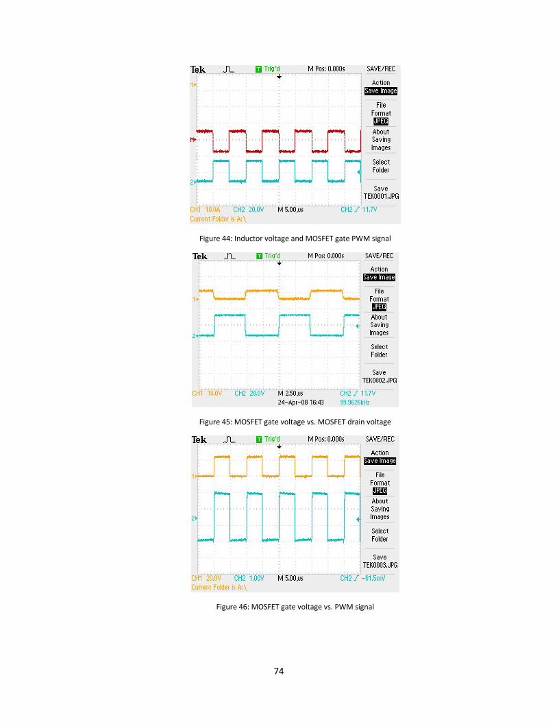
74
Figure 44: Inductor voltage and MOSFET gate PWM signal
Figure 45: MOSFET gate voltage vs. MOSFET drain voltage
Figure 46: MOSFET gate voltage vs. PWM signal

75
The output signals of the DC-DC converter imply accurate operation. When the switch is
off, the inductor charges in energy, and discharges when the switch is turned on. There is
minimal lag between the gate voltage of the MOSFET and the actual PWM signal. The drain
voltage versus the gate of the MOSFET is also observed.
Figure 47: Power vs. Duty Cycle
The resulting power curve from the open loop thevenin equivalent circuit is
demonstrated by the above figure. We see a large spike at approximately 71% duty cycle. This is
the moment when the voltage is still at its greatest while the current already has reached close
to its maximum value. With a working circuit, it would be desired to stay at this 71% duty cycle
or close to it. The microprocessor would oscillate between values of duty cycle around this 71%
duty cycle value. If at all the current or voltage coming from the power source decreases, the
duty cycle would move up from the 71% value until a lower value is obtained when observing
the power from the source. When the lower value is obtained, the duty cycle is increased again,
until a decrease can be seen. This oscillation would prove a successful design.

76
When the microprocessor is attached to the circuit it will output a PWM signal which
will allow the output power to be boosted like we intended. Also the Duty Cycle of the PWM
signal will sweep between its upper and lower limits in order to find where the maximum value
is. The problem is that when the Duty Cycle is sweeping between its limits it cannot seem to find
where the maximum value is and as a result will continue sweeping. There are a couple of places
where our tracking system could be flawed. The first thought is that there could be an error in
the computer code which doesn’t read that the power is changing and therefore will not
perform like expected. The microprocessor is hard to test without adding to the actual circuit
because the program which we used for programming the PIC doesn’t have a sufficient
simulator it which will allow for testing it in a circuit such as ours. Another reason why our
tracking system might not be working could be that the signal representing the current which
goes though the operational amplifier could have too small of a range to be picked up by the
microprocessor and therefore could be disrupting the results of the PIC.
Theoretical Operation
Theoretically when the PIC is working correctly it will track very closely where the
maximum peak power is. The PIC starts with a Duty Cycle of 50% and then will delay for roughly
a second to allow the value of the power across the load to either increase or decrease. Then
samples will be taken. At 50% the voltage will be around 12 V and the current will be around
.05A. Through the voltage divider the voltage going into the PIC will be roughly 2.7V, and the
current going in will be recorded as a voltage which is equal to a function of the current. This will
be roughly equal to .48V. These values will then go through an analog to digital converter which
will translate them to a digital representation. For roughly every 5mV there is a binary
representation. For the voltage the value would be close to 553, and for the current it will be
close to 98. Those digital representation are then multiplied together to give a digital

77
representation value of the power. Once this is found it is compared to the last stored value of
Power, if the new Power is higher, then the slope will be positive, and if the new value is lower,
then the slope will be negative. Next the PIC checks to see if the duty cycle was raised or
lowered the last time it was changed. If the duty cycle was increased the last time it was
changed then the slope of the duty cycle will be positive, and if the duty cycle was decreased the
last time it was changed then it will be negative. Next the PIC checks the derivative of the slope
of the Power over the Duty Cycle. If the slope ends up being positive then the duty cycle will be
increased, and if the slope ends up being negative the duty cycle will be decreased. The amount
that the duty cycle is changed by each time is 2.5% because this is the minimum allowable step
with an output frequency of 100kHz for the PWM going to the MOSFET. After this step where
the duty cycle increases or decreases the program will delay roughly another second to allow for
changes in the voltage, current, and power and will repeat the process again from taking
samples.

78
6.0 Future Recommendations
There were several problems encountered throughout the design of the circuit that we
would like to avoid in the future. First of all, the amount of time taken for design and testing
should have been concentrated more. There was a shorter design and test period, of 14 weeks
versus the 21 weeks typical for major qualifying project work. With such a serious time
constraint, it would have been beneficial to spend more time testing rather than taking the time
to make sure that each part was the ideal one for the circuit. Either way, more time or better
time management was a key issue that should definitely be worked out for future reference.
The problems with the parts obtained most likely stemmed from misunderstanding the
exact function of the component. It is vital to understand the design parameters associated with
each component to be sure that it does not breakdown or have a poor effect on the overall
circuit. In the future, it would be beneficial to eliminate the noise associated with the circuit.
There was no significant work in minimizing the noise in the circuit while attempting to
implement a working circuit both quickly, and efficiently. There are very few downsides with
taking the time and effort to design filters to decrease the inherent noise found in a switching
circuit. There are minimal power losses involved with adding filters, however the benefits to
cleaner signals would probably lead to more accurate and reliable results.
It would also be helpful to perform tests using actual solar panels. Doing such tests
would allow us to observe operation of a typical solar cell array, rather than thevenin
equivalents or simulator circuits. It would be useful to perform tests both indoor and outdoor to
observe both controlled and actual results for operation. Testing the circuit to perform
dynamically with light changes would give better more realistic results to see if the circuit is
performing as it actually should.

79
It is often useful to apply a solar panel power source to charge some sort of battery. This
can be seen in many typical applications that rely on the sun for power. In theory, when using a
battery in conjunction with solar cell operation, the battery holds the purpose of charging up
energy so that the system will be able to operate even without sunlight. This is useful for both
day and night situations, when in the evening there is no available light. With a charged battery,
the system will still be able to operate. As efficient as our design may be, without light, the
system receives no power, and will not function. It is also useful to charge a battery so that
there is a negative power source, and there is a different amount of voltage that can be used
without implementing something like a voltage divider or regulator to regulate the voltage, or
an amplifier to step it up.

80
7.0 Conclusion
Solar power continues to demonstrate its potential as a breakthrough for renewable
energy. As companies continue the research into solar power, the technology for them is
becoming more and more useful. One of the main concerns for fixing problems involved with
solar panel is of solar panel efficiency. A major goal for this solar panel application design was to
optimize efficiency whenever possible. This was done through meticulous examination of
product data sheets in order to obtain the most desirable part, particularly with the least
amount of associated power loss. Continued effort to maximize efficiency should always be
taken when designing solar applications to increase their usability and value.
The design of a maximum peak power tracking system proved to be a serious design
challenge. There are many factors involved when designing a circuit that relies on both digital
and analog aspects of circuitry. There are inherently many problems when designing a system
that relies heavily on digital circuitry. Errant code writing is one such problem, and can only be
remedied through trial and experience. Overall, the digital portion of the circuit was performing
as it should, however the marriage between the digital and analog portion was where we ran
into difficulty.
As there are many problems associated with digital design, there are also issues that
occur with analog implementation. With simulations of components, the transition to actual
design is ideally very easy. However, simulation does not always match implementation. The
first issue that caused problems was the MOSFET driver we had chosen. The first driver had all
the ideal functions of a driver and would have been perfect for the design, however the
packaging of the driver was too small to work with, and had to be sent out to be soldered onto
an adapter that converts the microchip to be compatible with an 8-dip setup. This took much

81
needed time. Also, even with added precaution (added a heatsink), several MOSFETs were
rendered useless when the circuit was in operation. These are problems that any design
engineer may encounter: faulty components, shipping delays and issues, and difficulty when
translating the designed schematics to the physical board.
Although there were many problems involved with the design process of this peak
power tracker, the process provided invaluable experience for the future. It will be very
beneficial to take the experience we have had to address potential problems that may arise in
our futures as design engineers. The experience was a valuable lesson in the problems that may
occur when designing, ordering, assembling, and testing parts. We would have preferred to
have a working prototype at the end of the design process, however the experience was
enlightening and challenging at the same time.

82
References Bogus, Klaus and Markvart, Tomas. Solar Electricity. Chichester, New York.Wiley Press,
1994.
LGBG Technology “Towards 20% Efficient Silicon Solar Cells.” 02 Oct 2005.
Aldous, Scott. “How Silicon in Solar Cells Works.” How Stuff Works. 02 Oct 2005.
Neville, Richard C. Solar Energy Conversion. The Netherlands: Elsevier Science, 1995.
Sayigh, A.A.M., ed. Solar Energy Engineering. New York, USA: Academic Press, 1977.
Richard Corkish, Solar Cells (Encyclopedia of Energy, 2004)
PV Technology “Photovoltaic: Sustainable Power for the World.” 08 Oct 2005.
Nation Center for Photovoltaics. “Turning Sunlight into Electricity.” 20 Oct. 2002.
Power Designer “DC-DC Converter Basic.” 02 Nov. 2005.
http://www.powerdesigners.com/InfoWeb/design_center/articles/DC-DC/
Hart, Daniel. Introduction to Power Electronics. Upper Saddle River, N.J.: Prentice Hall,
1997.
Six Ways to Measure Inductance, IOP Science, http://iopscience.iop.

83
Full Schematic
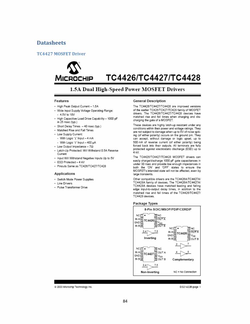
84
Datasheets
TC4427 MOSFET Driver

85
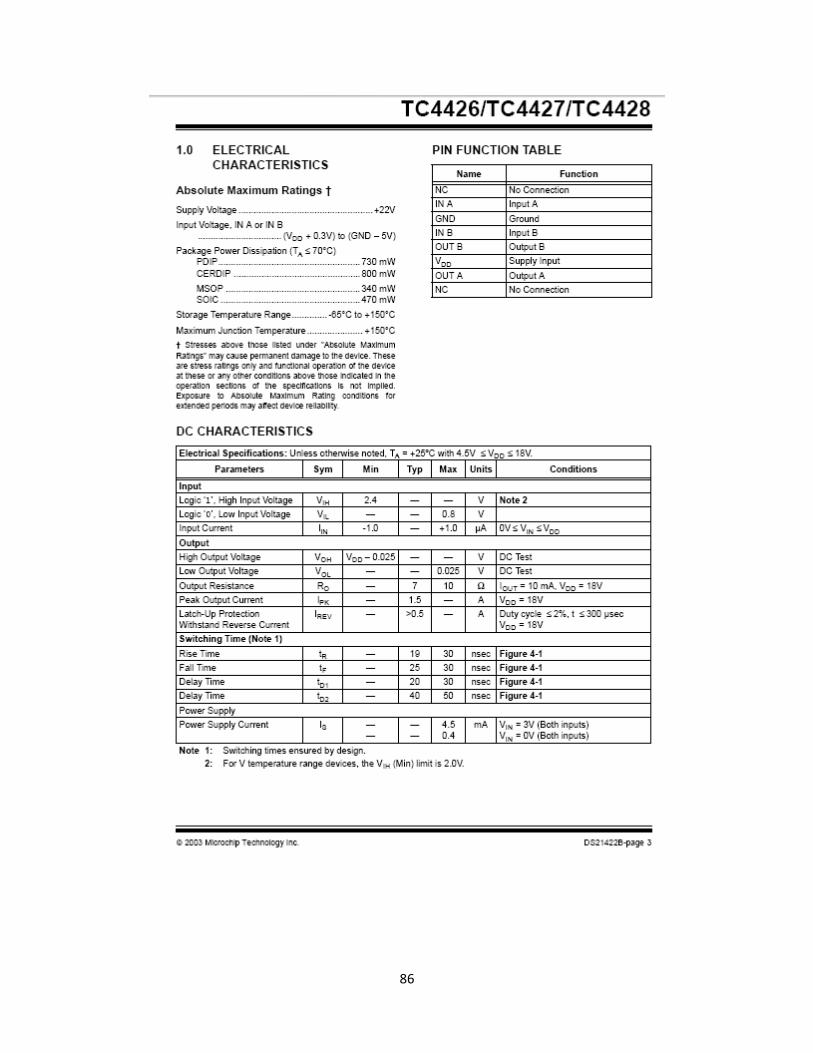
86

87

88

89

90

91
FDP6030 MOSFET

92

93

94

95
Schottky Diode
96

97

98
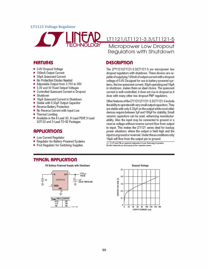
99
LT1121 Voltage Regulator

100

101

102
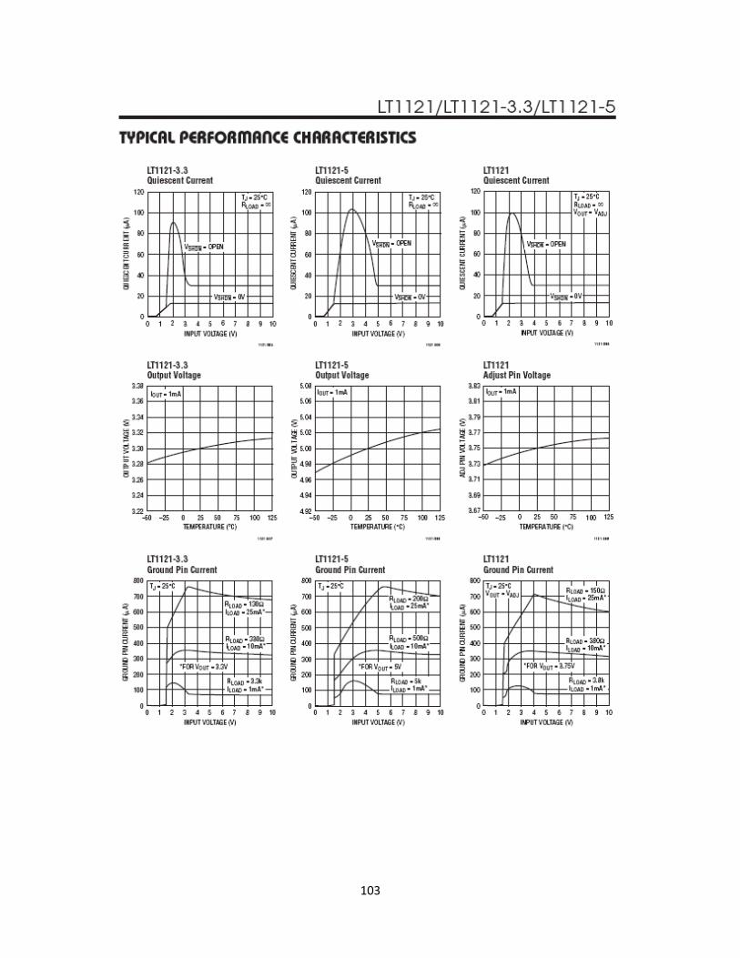
103
104
105

106
LMC6462 Differential Operational
Amplifier

107
108
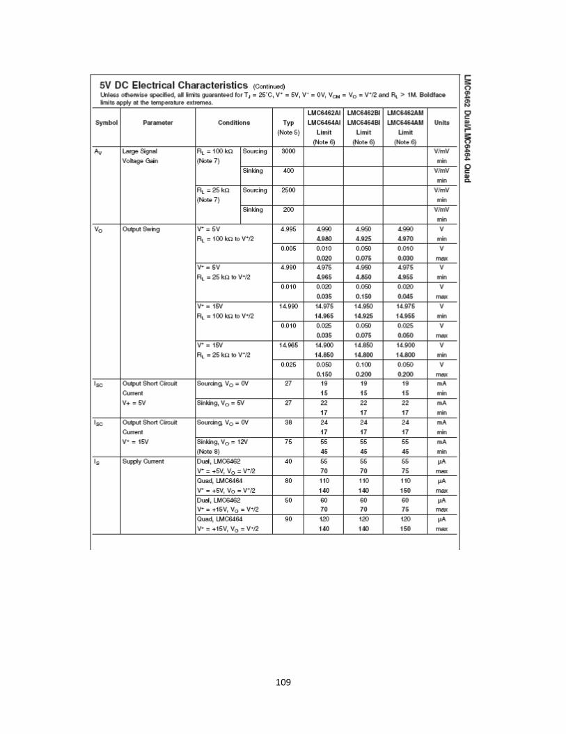
109
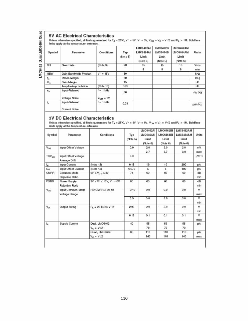
110
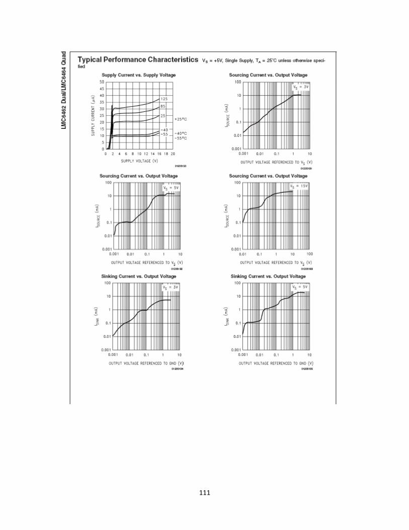
111
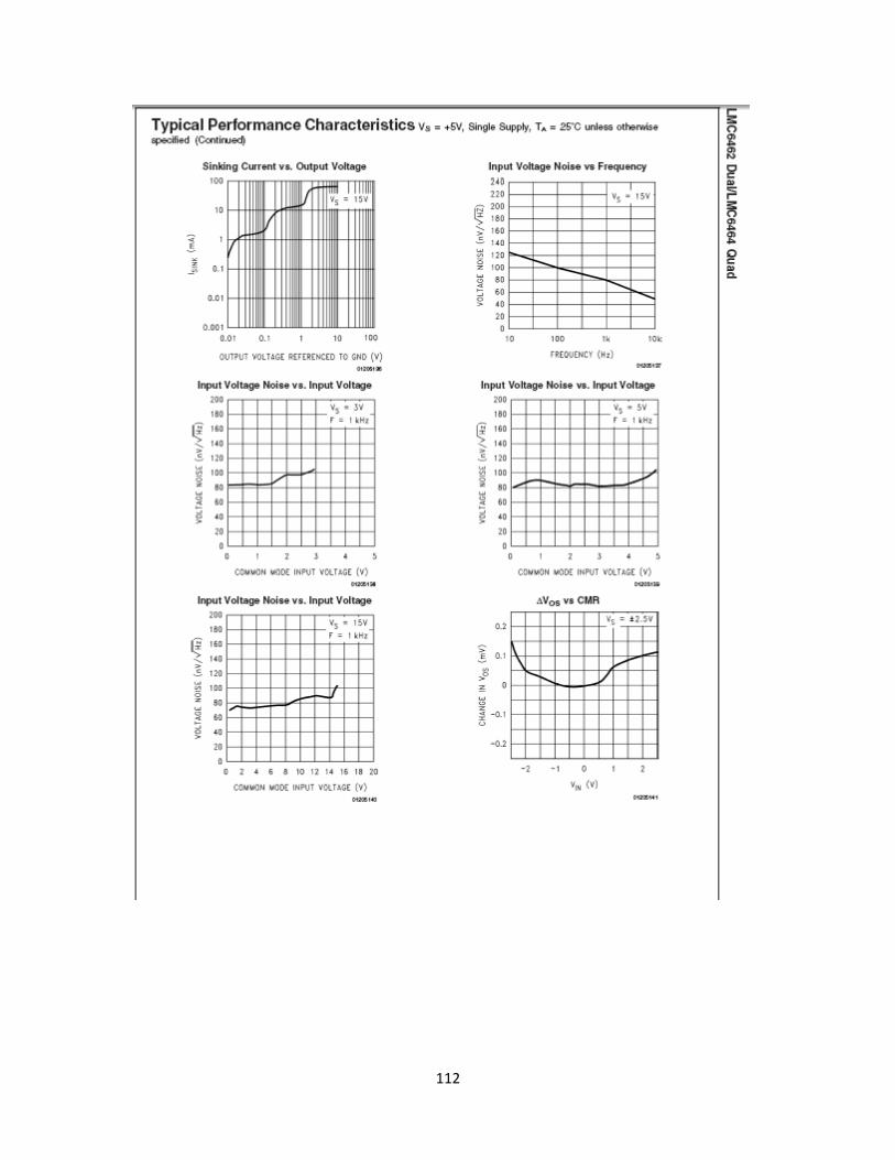
112

113
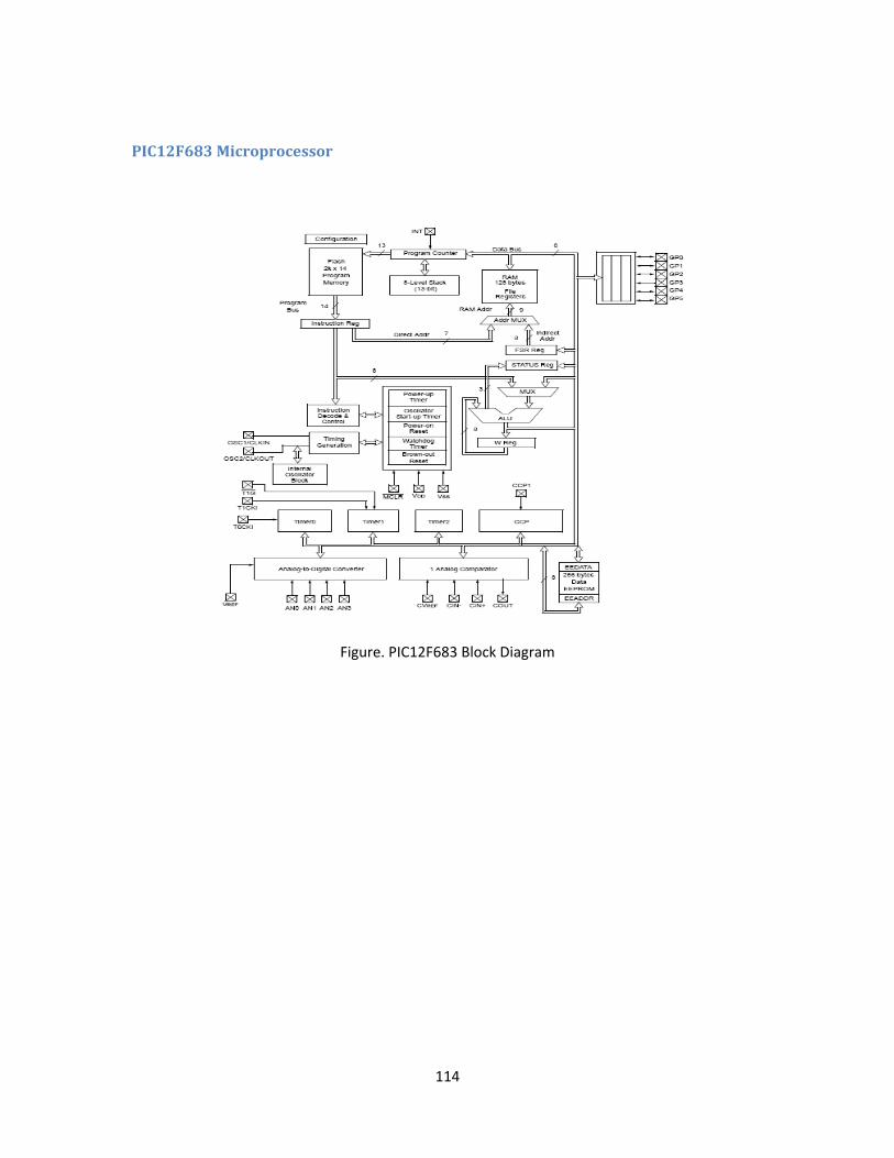
114
PIC12F683 Microprocessor
Figure. PIC12F683 Block Diagram
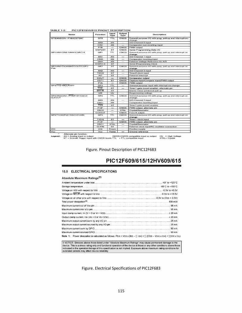
115
Figure. Pinout Description of PIC12F683
Figure. Electrical Specifications of PIC12F683

116
Figure. PIC Algorithm
Peak Power Tracking Code
;********************************************************************** ; This file is a basic code template for object module code * ; generation on the PIC12F683. This file contains the * ; basic code building blocks to build upon. As a project minimum * ; the 12F683.lkr file will also be required for this file to * ; correctly build. The .lkr files are located in the MPLAB * ; directory. * ; * ; If interrupts are not used all code presented between the * ; code section "INT_VECTOR and code section "MAIN" can be removed. * ; In addition the variable assignments for 'w_temp' and * ; 'status_temp' can be removed. * ; * ; If interrupts are used, as in this template file, the 12F683.lkr * ; file will need to be modified as follows: Remove the lines * ; CODEPAGE NAME=vectors START=0x0 END=0x4 PROTECTED * ; and * ; SECTION NAME=STARTUP ROM=vectors * ; and change the start address of the page0 section from 0x5 to 0x0 * ; *

117
; Refer to the MPASM User's Guide for additional information on * ; features of the assembler and linker (Document DS33014). * ; * ; Refer to the respective PIC data sheet for additional * ; information on the instruction set. * ; * ;********************************************************************** ; * ; Filename: PIC12F683.asm * ; Date: 4/07/08 * ; File Version: * ; * ; Author: Michael Miller & Daniel Butay * ; Company: * ; * ; * ;********************************************************************** ; * ; Files required: * ; 12F683.lkr * ; * ; * ;********************************************************************** ; * ; Notes: This code will allow for peak power tracking from a * ; Photovoltaic array going through a boost converter. * ; * ; * ; * ;********************************************************************** list p=12F683 ; list directive to define processor #include <p12F683.inc> ; processor specific variable definitions errorlevel -302 ; suppress message 302 from list file __CONFIG _FCMEN_ON & _IESO_OFF & _CP_OFF & _CPD_OFF & _BOD_OFF & _MCLRE_ON & _WDT_OFF & _PWRTE_ON & _INTRC_OSC_NOCLKOUT ; '__CONFIG' directive is used to embed configuration word within .asm file. ; The lables following the directive are located in the respective .inc file. ; See data sheet for additional information on configuration word settings. ;***** VARIABLE DEFINITIONS (examples) ; example of using Shared Uninitialized Data Section INT_VAR UDATA_SHR ;w_temp RES 1 ; variable used for context saving status_temp RES 1 ; variable used for context saving
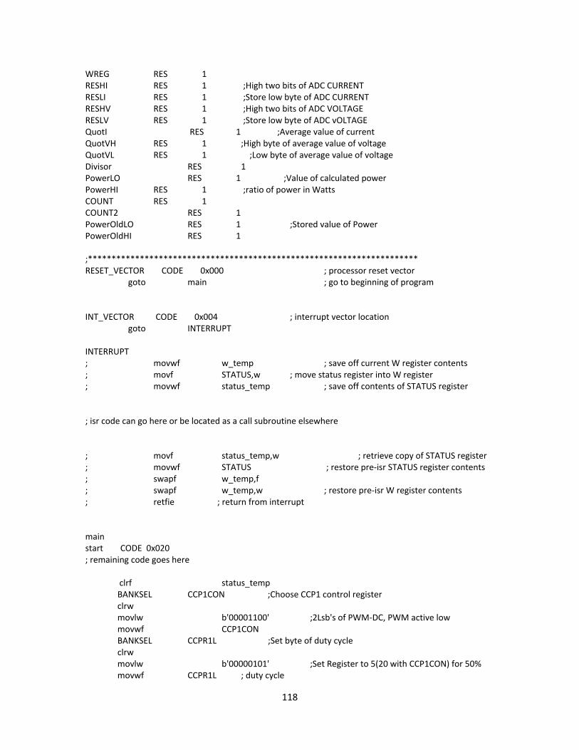
118
WREG RES 1 RESHI RES 1 ;High two bits of ADC CURRENT RESLI RES 1 ;Store low byte of ADC CURRENT RESHV RES 1 ;High two bits of ADC VOLTAGE RESLV RES 1 ;Store low byte of ADC vOLTAGE QuotI RES 1 ;Average value of current QuotVH RES 1 ;High byte of average value of voltage QuotVL RES 1 ;Low byte of average value of voltage Divisor RES 1 PowerLO RES 1 ;Value of calculated power PowerHI RES 1 ;ratio of power in Watts COUNT RES 1 COUNT2 RES 1 PowerOldLO RES 1 ;Stored value of Power PowerOldHI RES 1 ;********************************************************************** RESET_VECTOR CODE 0x000 ; processor reset vector goto main ; go to beginning of program INT_VECTOR CODE 0x004 ; interrupt vector location goto INTERRUPT INTERRUPT ; movwf w_temp ; save off current W register contents ; movf STATUS,w ; move status register into W register ; movwf status_temp ; save off contents of STATUS register ; isr code can go here or be located as a call subroutine elsewhere ; movf status_temp,w ; retrieve copy of STATUS register ; movwf STATUS ; restore pre-isr STATUS register contents ; swapf w_temp,f ; swapf w_temp,w ; restore pre-isr W register contents ; retfie ; return from interrupt main start CODE 0x020 ; remaining code goes here clrf status_temp BANKSEL CCP1CON ;Choose CCP1 control register clrw movlw b'00001100' ;2Lsb's of PWM-DC, PWM active low movwf CCP1CON BANKSEL CCPR1L ;Set byte of duty cycle clrw movlw b'00000101' ;Set Register to 5(20 with CCP1CON) for 50% movwf CCPR1L ; duty cycle

119
Init NOP call PWMinit ;Initialize PWM call getvolts ;Get 4 samples of voltage call average ;Average 4 samples call getamps ;Get 4 Samples of Current call averageI ;Average 4 samples ;go call mult ;Multiply Current and Voltage to get Power call Compare call storePower call Delay2 call Delay2 call Delay2 goto Init ;*************************** Delay2 movlw 0x3FFF movwf COUNT repeat call Delay decfsz COUNT,1 goto repeat return ;*************************** storePower movf PowerHI,0 movwf PowerOldHI movf PowerLO,0 movwf PowerOldLO return ;*************************** ;*************************** PWMinit BANKSEL OSCCON ;Choose OSCCON register clrf WREG movwf OSCCON ;clear oscillator control register movlw b'01100001' ;set Fosc to 4MHz & set to internal oscillator movwf OSCCON BANKSEL TRISIO ;Choose Register which makes pins I or O clrw movwf TRISIO ;clear TRIS register movlw b'00111111' ;disable CCP1 movwf TRISIO BANKSEL PR2 ;SELECT PERIOD REGISTER movlw b'00001001' ;Set PR2 to 9 so PWM frequency will be 100kHz movwf PR2 Call SetDuty BANKSEL PIR1 ;Clear interrupt flag bit of TMR2 movlw 00h movwf PIR1 BANKSEL T2CON movlw 04h

120
movwf T2CON TMR2OF
btfss PIR1,b'1' ;Waits until Timer 2 goes through goto TMR2OF ;One cycle (overflows). Then BANKSEL TRISIO ;enables CCP1 pin output driver movlw b'00111011' movwf TRISIO return ;*************************** ;************************** getamps movlw 0x04 ;Set the value of samples taken movwf COUNT fourtimesI clrf RESHI ;Clear hi and low bye of current sample clrf RESLI call initADCi call STORERESULTI decfsz COUNT,1 goto fourtimesI return ;************************** ;************************** getvolts movlw 0x04 ;Set the value of voltage samples taken movwf COUNT fourtimesV clrf RESLV clrf RESHV ;Clear hi and low byte of Voltage sample call initADCv call STORERESULTV decfsz COUNT,1 goto fourtimesV return ;************************** ;************************** initADCi BANKSEL TRISIO BSF TRISIO,0 ;Set GP0 to input BANKSEL ANSEL clrw movlw b'01110001' ; Configure pin 7 as analog inputs & select conversion clock movwf ANSEL ;for FOLLOW INTERNAL OSCILLATOR BANKSEL ADCON0 clrw movlw b'10000001' ;Set Vref, select channel gp0, select Right justified results movwf ADCON0 ;

121
BCF PIR1,b'110' ;CLEAR ADC INTERRUPT ;delay aquisition time at least 4.67uS call Delay continuei BANKSEL ADCON0 clrw movlw b'00000010' ;Set GO/DONE bit to start ADC xorwf ADCON0,1 POLLGODONEi btfsc ADCON0,b'1' ;waits til ADC is done goto POLLGODONEi return ;************************** ;************************** initADCv BANKSEL TRISIO BSF TRISIO,0 ;Set GP0 to input BANKSEL ANSEL clrw movlw b'01110010' ; Configure pin 6 as analog inputs & select conv clock movwf ANSEL ;for FOLLOW INTERNAL OSCILLATOR BANKSEL ADCON0 clrw movlw b'10000101' ;Set Vref, select channel gp0, select Right justified results movwf ADCON0 ; BCF PIR1,b'110' ;CLEAR ADC INTERRUPT call Delay ; ;delay aquisition time at least 4.67uS continuev BANKSEL ADCON0 clrw movlw b'00000010' ;Set GO/DONE bit to start ADC xorwf ADCON0,1 POLLGODONEv btfsc ADCON0,b'1' ;waits til ADC is done goto POLLGODONEv return ;************************** ;************************** STORERESULTI ;Store current value CALL STOREADRESLI btfsc STATUS,b'0' goto addone cont BANKSEL ADRESH btfss ADRESH, b'1' ;check two high bits of ADC result

122
btfsc ADRESH, b'0' CALL STOREADRESHI return addone movlw 0x01 addwf RESHI,1 bcf STATUS,b'0' goto cont ;************************** ;************************** STORERESULTV ;Store voltage value CALL STOREADRESLV BANKSEL ADRESH btfss ADRESH,b'1' ;check two high bits of ADC result btfsc ADRESH,b'0' CALL STOREADRESHV return ;*************************** ;*************************** STOREADRESHI ;Store the High two bits of ADC CURRENT btfsc STATUS,b'0' goto rtrnI movlw 0x01 addwf RESHI,1 rtrnI movf ADRESH,0 addwf RESHI,1 return ;*************************** ;*************************** STOREADRESLI ;Store the low Byte of ADc CURRENT BANKSEL ADRESL movf ADRESL,0 ;Move low byte to W_reg addwf RESLI,1 ;Add and store in RESLI return ;*************************** ;*************************** STOREADRESHV ;Store the High two bits of ADC VOLTS btfss STATUS,b'0' goto rtrnV movlw 0x01 addwf RESHV,1 rtrnV movf ADRESH,0 addwf RESHV,1 return ;*************************** ;*************************** STOREADRESLV ;Store the low Byte of ADC VOLTAGE

123
BANKSEL ADRESL movf ADRESL,0 addwf RESLV,1 return ;*************************** ;*************************** averageV bcf STATUS,b'0' ;divide by continuous subtraction clrf QuotVH clrf QuotVL movlw 0x04 movwf Divisor DivideV movf Divisor,0 ; setup for subtraction subwf RESLV,1 ; RESLV = RESLV - Divisor btfss STATUS,b'0' goto BorrowV goto Div_2V BorrowV movlw 0x01 subwf RESHV,1 ; use subtract instead of decf btfss STATUS,b'0' ; ... because it sets the carry goto DoneV ; generated a borrow so finish Div_2V incf QuotVL,1 ; add one and loop again btfsc STATUS,b'10' incf QuotVH,1 goto DivideV DoneV return ;*************************** ;*************************** averageI bcf STATUS,b'0' ;divide by contiuous subtraction clrf QuotI movlw 0x04 movwf Divisor DivideI movf Divisor,0 ; setup for subtraction subwf RESLI,1 ;RESLI = RESLI - Divisor btfss STATUS,b'0' goto BorrowI goto Div_2I BorrowI movlw 0x01 subwf RESHI,1 ;use subtract instead of decf btfss STATUS,b'0' ; ... because it sets the carry goto DoneI ;generated a borrow so finish Div_2I incf QuotI,1 ;add one and loop again goto DivideI DoneI

124
return ;*************************** ;*************************** mult clrf PowerLO ;Clears hi and low bytes of power register clrf PowerHI
movf QuotI,0 ;Move average current value to a separate movwf COUNT2 ;register bcf STATUS,0 ;CLEAR CARRY BIT again movf QuotVL,0 ;Add low byte of averaged voltage to low byte of addwf PowerLO,0 ;power register movwf PowerLO btfsc STATUS,0 ;Test the carry bit incf PowerHI,1 ;Increment the high byte of Power reg if carry is set movlw 0x02 btfsc QuotVH,1 ;Test if high byte of averaged voltage has a value addwf PowerHI,1 ;add that value if yes,skip if no btfsc QuotVH,0 incf PowerHI,1 decfsz COUNT2,1 ;repeat for value of AMPS register goto again return ;*************************** ; ************************** Delay movlw 0xFF movwf COUNT2 Delay1 decfsz COUNT2,1 ; Decrement Memory And Skip When Zero goto Delay1 return ; ************************** ;*************************** SetDuty call chk_lmts btfsc status_temp,b'11' goto raiseDC btfsc status_temp,b'10' goto lowerDC btfss status_temp,b'1' ;test if duty cycle was increased or decreased last goto pos ;if set the duty cycle was decreased last btfss status_temp,b'0' ;test if power was inc or dec last goto lowerDC ;if not set the power is higher goto raiseDC ;if set the power is lower pos ;if not set the duty cycle was increased last btfss status_temp,b'0' ;test if power was inc or dec last goto raiseDC ;if not set the power is higher goto lowerDC ;if set the power is lower lowerDC bcf status_temp,b'10'
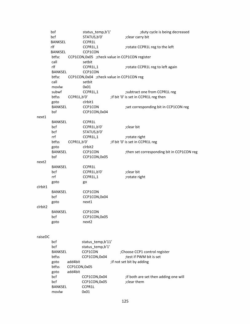
125
bsf status_temp,b'1' ;duty cycle is being decreased bcf STATUS,b'0' ;clear carry bit BANKSEL CCPR1L rlf CCPR1L,1 ;rotate CCPR1L reg to the left BANKSEL CCP1CON btfsc CCP1CON,0x05 ;check value in CCP1CON register call setbit rlf CCPR1L,1 ;rotate CCPR1L reg to left again BANKSEL CCP1CON btfsc CCP1CON,0x04 ;check value in CCP1CON reg call setbit movlw 0x01 subwf CCPR1L,1 ;subtract one from CCPR1L reg btfss CCPR1L,b'0' ;if bit '0' is set in CCPR1L reg then goto clrbit1 BANKSEL CCP1CON ;set corresponding bit in CCP1CON reg bsf CCP1CON,0x04 next1 BANKSEL CCPR1L bcf CCPR1L,b'0' ;clear bit bcf STATUS,b'0' rrf CCPR1L,1 ;rotate right btfss CCPR1L,b'0' ;if bit '0' is set in CCPR1L reg goto clrbit2 BANKSEL CCP1CON ;then set corresponding bit in CCP1CON reg bsf CCP1CON,0x05 next2 BANKSEL CCPR1L bcf CCPR1L,b'0' ;clear bit rrf CCPR1L,1 ;rotate right goto go clrbit1 BANKSEL CCP1CON bcf CCP1CON,0x04 goto next1 clrbit2 BANKSEL CCP1CON bcf CCP1CON,0x05 goto next2 raiseDC bcf status_temp,b'11' bcf status_temp,b'1' BANKSEL CCP1CON ;Choose CCP1 control register btfss CCP1CON,0x04 ;test if PWM bit is set goto add4bit ;if not set bit by adding btfss CCP1CON,0x05 goto add4bit bcf CCP1CON,0x04 ;if both are set then adding one will bcf CCP1CON,0x05 ;clear them BANKSEL CCPR1L movlw 0x01

126
addwf CCPR1L,1 ;add one to upper byte of PWM duty cycle bits goto go add4bit movlw 0x10 addwf CCP1CON,1 goto go add5bit movlw 0x20 addwf CCP1CON,1 goto go go return ;********************************** ;********************************** Compare movf PowerHI,0 subwf PowerOldHI,0 ;subtract high byte of Pnew from Pold btfsc STATUS,b'0' ;if clear new power is less than old power goto decreased movf PowerLO,0 ;if set new power is equal or higher subwf PowerOldLO,0 ;subtract low byte of new power from old power btfsc STATUS,b'0' ;if clear new power is less than old power goto decreased bsf status_temp,b'0' ;if set than new power is higher than old power ret return decreased bcf status_temp,b'0' goto ret ;********************************* ;********************************* setbit BANKSEL CCPR1L ;if set then increment CCPR1L reg bsf CCPR1L,b'0' return ;********************************** ;********************************** chk_lmts BANKSEL CCPR1L rlf CCPR1L,1 bcf CCPR1L,0x00 BANKSEL CCP1CON btfsc CCP1CON,0x05 call setbit BANKSEL CCPR1L rlf CCPR1L,1 BANKSEL CCP1CON btfsc CCP1CON,0x04 call setbit BANKSEL CCPR1L movlw 0x1A subwf CCPR1L,0 btfsc STATUS,b'10'

127
bsf status_temp,b'10' movlw 0x00 subwf CCPR1L,0 btfsc STATUS,b'10' bsf status_temp,b'11' bcf CCPR1L,b'0' bcf STATUS,b'0' rrf CCPR1L,1 bcf CCPR1L,b'0' bcf STATUS,b'0' rrf CCPR1L,1 return ;************************************* ;Forever Loop PROG btfss PIR1,b'0' goto Init ; initialize eeprom locations EE CODE 0x2100 DE 0x00, 0x01, 0x02, 0x03 END ; directive 'end of program'
DC-DC Converter Simulation DCDCConverter W/Filter VIN 1 0 12V .SUBCKT SWITCH 10 20 30 40 S 10 20 30 40 ZWICK .MODEL ZWICK VSWITCH(RON=1 ROFF=1MEG) CS 10 15 .1u IC=0 RS 15 20 300 .ENDS X1 5 0 A 0 SWITCH VC1 A 0 PULSE(0 2 0 1u 1u 50u 100u) D 5 6 D1 .MODEL D1 D(RS=.1 BV=1000) CSD 5 25 .1u IC=0 RSD 25 6 300 Rs 3 4 .1 L 4 5 500u IC=0 C 6 0 330u IC=0 R 6 0 20 RF 1 2 .1 LF 2 3 50u IC=0 CF 3 0 10u IC=0 .PROBE .TRAN 15m 15m 0 10u UIC .END