max14736max14737 precision, ultraast, lo spply crrent ... · max14736max14737 precision, ultraast,...
TRANSCRIPT

General DescriptionThe MAX14736/MAX14737 overvoltage-protection (OVP) devices guard battery-powered modules in portable devices against overvoltage faults. The low 15mΩ (typ) on-resistance, as well as the low 13µA (typ) quiescent supply current of the devices, minimize power consump-tion, making them an ideal choice for low-power systems. Additionally, the devices feature a precision overvoltage-lockout (OVLO) threshold, ultra-fast response time, and surge suppression to ±35V, which serve to provide excel-lent protection against even high slew-rate, high-voltage transients.The integrated power transistor in the devices is a p-channel device, but the intrinsic body diode from OUT to IN is removed through appropriate design techniques. Consequently, when the switch is in the off state, reverse-current blocking that is inherent to the devices. The MAX14736/MAX14737 feature a push-pull POK output, which is driven low if either an overvoltage, undervoltage, or thermal fault is detected; or if the device is placed into shutdown mode. The MAX14736 has an active-low enable pin (EN), while the enable pin (EN) on the MAX14737 is active high.When the enable pin is driven to the active state, the device is enabled. When driven to the inactive state, the device is placed in a low-power shutdown mode and the switch is kept in the off state. The MAX14736/MAX14737 are offered in a small, 9-bump (1.34mm x 1.36mm) wafer-level package (WLP) and oper-ate over the -40°C to +85°C extended temperature range.
Benefits and Features Protects Battery-Connected Modules with Minimal
Power Consumption• Wide Operating Input Voltage: +2.1V to +5.5V• 4.5A Continuous Current Capability• Integrated 15mΩ (typ) pFET• Ultra-Low Supply Current: 13µA (typ)
Allows Precise Design in OVLO Implementation• Preset Accurate Internal OVP Thresholds
• MAX14736: 4.7V ±2.0%• MAX14737: 5.2V ±2.0%
Increases System Reliability Through Premium Security• Surge Immunity to ±35V• Soft-Start to Minimize Inrush Current• Output Hot Plug-In Protection• Thermal Shutdown• Ultra-Fast OVP Response Time: 200ns (typ)
Minimizes Board Space by Compact WLP• 9-Bump 1.34mm x 1.36mm WLP
Applications Smartphones Tablet PCs e-Readers
Ordering Information appears at end of data sheet.
19-7517; Rev 0; 5/15
Typical Application Circuit
PMIC
GND
MAX14737
POK
OUT
OUT
OUT
EN
IN
IN
IN
0.1µF1kΩ
0.1µF
CHGIN
BATIN
BYP
SYS
BYPASS
SYSTEM
MICRO-B USBHIDDEN BATTERY
MAX14736/MAX14737 Precision, Ultra-Fast, Low Supply Current, Bidirectional Overvoltage Protector
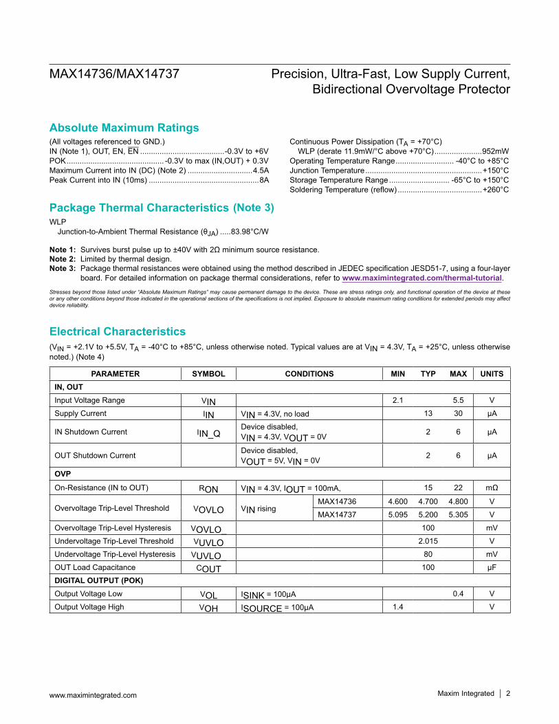
(All voltages referenced to GND.)IN (Note 1), OUT, EN, EN .......................................-0.3V to +6VPOK ............................................. -0.3V to max (IN,OUT) + 0.3VMaximum Current into IN (DC) (Note 2) ..............................4.5APeak Current into IN (10ms) ...................................................8A
Continuous Power Dissipation (TA = +70°C) WLP (derate 11.9mW/°C above +70°C) ......................952mW
Operating Temperature Range ........................... -40°C to +85°CJunction Temperature ......................................................+150°CStorage Temperature Range ............................ -65°C to +150°CSoldering Temperature (reflow) .......................................+260°C
WLP Junction-to-Ambient Thermal Resistance (θJA) .....83.98°C/W
(Note 3)
(VIN = +2.1V to +5.5V, TA = -40°C to +85°C, unless otherwise noted. Typical values are at VIN = 4.3V, TA = +25°C, unless otherwise noted.) (Note 4)
Electrical Characteristics
PARAMETER SYMBOL CONDITIONS MIN TYP MAX UNITSIN, OUTInput Voltage Range VIN 2.1 5.5 V
Supply Current IIN VIN = 4.3V, no load 13 30 µA
IN Shutdown Current IIN_QDevice disabled,VIN = 4.3V, VOUT = 0V 2 6 µA
OUT Shutdown Current Device disabled,VOUT = 5V, VIN = 0V 2 6 µA
OVP
On-Resistance (IN to OUT) RON VIN = 4.3V, IOUT = 100mA, 15 22 mΩ
Overvoltage Trip-Level Threshold VOVLO VIN risingMAX14736 4.600 4.700 4.800 V
MAX14737 5.095 5.200 5.305 V
Overvoltage Trip-Level Hysteresis VOVLO_ 100 mV
Undervoltage Trip-Level Threshold VUVLO 2.015 V
Undervoltage Trip-Level Hysteresis VUVLO_ 80 mV
OUT Load Capacitance COUT 100 µF
DIGITAL OUTPUT (POK)Output Voltage Low VOL ISINK = 100µA 0.4 V
Output Voltage High VOH ISOURCE = 100µA 1.4 V
MAX14736/MAX14737 Precision, Ultra-Fast, Low Supply Current, Bidirectional Overvoltage Protector
www.maximintegrated.com Maxim Integrated 2
Note 1: Survives burst pulse up to ±40V with 2Ω minimum source resistance.Note 2: Limited by thermal design.Note 3: Package thermal resistances were obtained using the method described in JEDEC specification JESD51-7, using a four-layer
board. For detailed information on package thermal considerations, refer to www.maximintegrated.com/thermal-tutorial.
Absolute Maximum Ratings
Stresses beyond those listed under “Absolute Maximum Ratings” may cause permanent damage to the device. These are stress ratings only, and functional operation of the device at these or any other conditions beyond those indicated in the operational sections of the specifications is not implied. Exposure to absolute maximum rating conditions for extended periods may affect device reliability.
Package Thermal Characteristics
(VIN = +2.1V to +5.5V, TA = -40°C to +85°C, unless otherwise noted. Typical values are at VIN = 4.3V, TA = +25ºC, unless otherwise noted.) (Note 4)
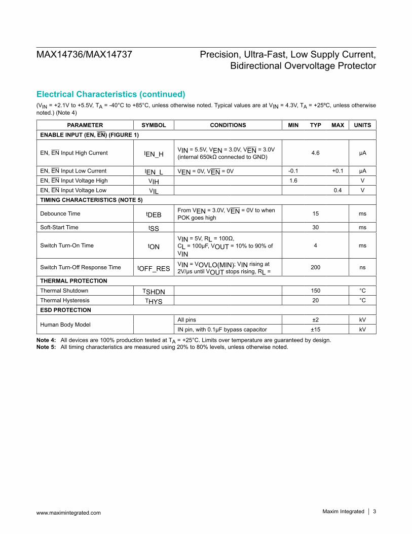
Note 4: All devices are 100% production tested at TA = +25°C. Limits over temperature are guaranteed by design.Note 5: All timing characteristics are measured using 20% to 80% levels, unless otherwise noted.
PARAMETER SYMBOL CONDITIONS MIN TYP MAX UNITSENABLE INPUT (EN, EN) (FIGURE 1)
EN, EN Input High Current IEN_HVIN = 5.5V, VEN = 3.0V, VEN = 3.0V (internal 650kΩ connected to GND)
4.6 µA
EN, EN Input Low Current IEN_L VEN = 0V, VEN = 0V -0.1 +0.1 µA
EN, EN Input Voltage High VIH 1.6 V
EN, EN Input Voltage Low VIL 0.4 V
TIMING CHARACTERISTICS (NOTE 5)
Debounce Time tDEBFrom VEN = 3.0V, VEN = 0V to when POK goes high
15 ms
Soft-Start Time tSS 30 ms
Switch Turn-On Time tONVIN = 5V, RL = 100Ω,CL = 100µF, VOUT = 10% to 90% of VIN
4 ms
Switch Turn-Off Response Time tOFF_RESVIN = VOVLO(MIN); VIN rising at 2V/µs until VOUT stops rising, RL =
200 ns
THERMAL PROTECTIONThermal Shutdown TSHDN 150 °C
Thermal Hysteresis THYS 20 °C
ESD PROTECTION
Human Body ModelAll pins ±2 kV
IN pin, with 0.1µF bypass capacitor ±15 kV
MAX14736/MAX14737 Precision, Ultra-Fast, Low Supply Current, Bidirectional Overvoltage Protector
www.maximintegrated.com Maxim Integrated 3
Electrical Characteristics (continued)

Figure 1. Timing Diagram
tDEB
OUT
IN
tOFF_RES
EN
VIN_MIN
THERMAL SHUTDOWN
tDEB
tDEB
VOVLO
tSS tDEB
POK
tON
MAX14736/MAX14737 Precision, Ultra-Fast, Low Supply Current, Bidirectional Overvoltage Protector
www.maximintegrated.com Maxim Integrated 4
(VIN = 4.3V, TA = +25ºC, unless otherwise noted.)
0.8
1.0
1.2
1.4
1.6
1.8
2 2.5 3 3.5 4 4.5 5 5.5
NORM
ALIZ
ED O
N-RE
SIST
ANCE
INPUT VOLTAGE (V)
NORMALIZED ON-RESISTANCEvs. INPUT VOLTAGE
NORMALIZED TO VIN = 4.3V
toc04
MAX14737IOUT = 1A
0
2
4
6
8
10
12
14
16
18
20
0.0 0.5 1.0 1.5 2.0 2.5 3.0 3.5 4.0 4.5 5.0 5.5
SUPP
LY C
URRE
NT (µ
A)
IN VOLTAGE (V)
IN SUPPLY CURRENT vs. SUPPLY VOLTAGE
VEN = VIN
toc01
TA = -40ºC
TA = +25ºC
TA = +85ºC
MAX14737
0.5
0.6
0.7
0.8
0.9
1.0
1.1
1.2
1.3
1.4
1.5
-40 -15 10 35 60 85
NORM
ALIZ
EDON
-RES
ISTA
NCE
TEMPERATURE (°C)
NORMALIZED ON-RESISTANCEvs. TEMPERATURE
NORMALIZED TO +25°C
toc02
IOUT = 1A
0.90
0.95
1.00
1.05
1.10
1.15
1.20
0.0 0.5 1.0 1.5 2.0 2.5 3.0 3.5 4.0 4.5
NORM
ALIZ
ED O
N-RE
SIST
ANCE
OUTPUT CURRENT (A)
NORMALIZED ON-RESISTANCEvs. OUTPUT CURRENT toc03
NORMALIZED TO 0.1A LOAD CURRENT
0.98
0.99
1.00
1.01
1.02
-40 -15 10 35 60 85
NORM
ALIZ
ED O
VLO
THRE
SHOL
D
°
NORMALIZED OVLO THRESHOLDvs. TEMPERATURE toc05
NORMALIZED TO +25°C
0.0
0.2
0.4
0.6
0.8
1.0
1.2
1.4
1.6
1.8
2.0
-40 -15 10 35 60 85
NORM
ALIZ
ED D
EBOU
NCE
TIME
TEMPERATURE (°C)
NORMALIZED DEBOUNCE TIMEvs. TEMPERATURE toc06
NORMALIZED TO +25°C
MAX14736/MAX14737 Precision, Ultra-Fast, Low Supply Current, Bidirectional Overvoltage Protector
Maxim Integrated 5www.maximintegrated.com
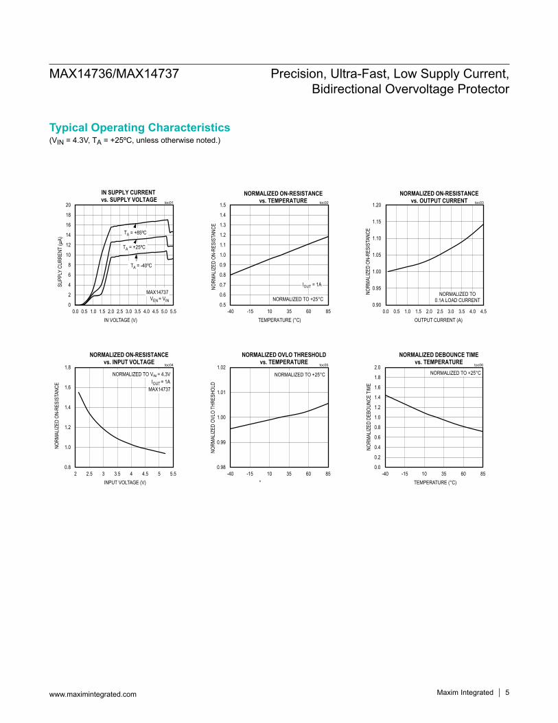
Typical Operating Characteristics
(VIN = 4.3V, TA = +25ºC, unless otherwise noted.)
2V/div
2V/div
2V/div
toc10
2µs/div
OVERVOLTAGE-FAULT RESPONSE
100mA/div
MAX14737
0V
VIN
VOUT
IOUT
VPOK
0V
0A
5V/div
100mA/div
5V/div
toc07
10ms/div
VIN
VPOK
POWER-UP RESPONSECL = 100µF
VOUT
2V/div
IOUT
5V/div
5V/div
1A/div
toc08
10ms/div
VIN
VPOK
POWER-UP RESPONSECL = 1000µF
VOUT
2V/div
IOUT
5V/div
5V/div
2V/div
toc09
10ms/div
VIN
VOUT
OVERVOLTAGE-FAULT RESPONSE
VPOK
100mA/divIOUT
MAX14737MAX14737
10V/div
toc11
10µs/div
VIN
35V SURGE TEST WAVEFORMWITHOUT MAX14737
5V/div (AC-COUPLED)
5V/div
toc12
10µs/div
VIN
VOUT
35V SURGE TEST WAVEFORMWITH MAX14737
VOUT INITIAL VOLTAGE = 2.5V
MAX14736/MAX14737 Precision, Ultra-Fast, Low Supply Current, Bidirectional Overvoltage Protector
Maxim Integrated 6www.maximintegrated.com
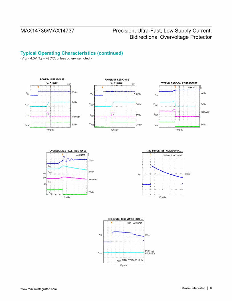
Typical Operating Characteristics (continued)
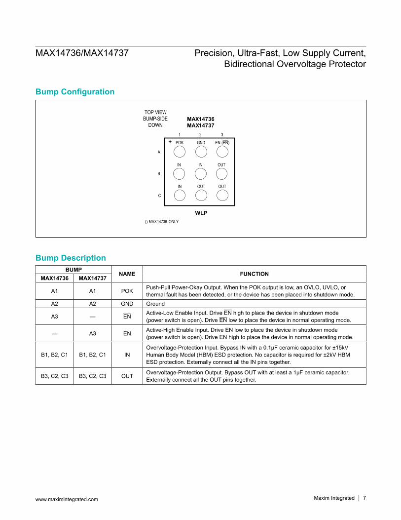
BUMPNAME FUNCTION
MAX14736 MAX14737
A1 A1 POK Push-Pull Power-Okay Output. When the POK output is low, an OVLO, UVLO, or thermal fault has been detected, or the device has been placed into shutdown mode.
A2 A2 GND Ground
A3 — EN Active-Low Enable Input. Drive EN high to place the device in shutdown mode (power switch is open). Drive EN low to place the device in normal operating mode.
— A3 EN Active-High Enable Input. Drive EN low to place the device in shutdown mode (power switch is open). Drive EN high to place the device in normal operating mode.
B1, B2, C1 B1, B2, C1 INOvervoltage-Protection Input. Bypass IN with a 0.1µF ceramic capacitor for ±15kV Human Body Model (HBM) ESD protection. No capacitor is required for ±2kV HBM ESD protection. Externally connect all the IN pins together.
B3, C2, C3 B3, C2, C3 OUT Overvoltage-Protection Output. Bypass OUT with at least a 1µF ceramic capacitor. Externally connect all the OUT pins together.
WLP
TOP VIEWBUMP-SIDE
DOWNMAX14736MAX14737
+ POK
1
IN
2
IN
3
GND
A
IN
B
OUT
C
EN (EN)
OUT
OUT
() MAX14736 ONLY
MAX14736/MAX14737 Precision, Ultra-Fast, Low Supply Current, Bidirectional Overvoltage Protector
www.maximintegrated.com Maxim Integrated 7
Bump Configuration
Bump Description
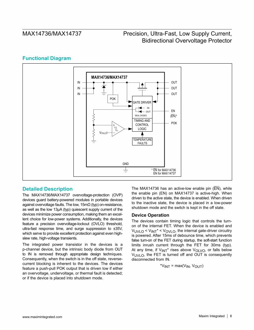
Detailed DescriptionThe MAX14736/MAX14737 overvoltage-protection (OVP) devices guard battery-powered modules in portable devices against overvoltage faults. The low, 15mΩ (typ) on-resistance, as well as the low 13µA (typ) quiescent supply current of the devices minimize power consumption, making them an excel-lent choice for low-power systems. Additionally, the devices feature a precision overvoltage-lockout (OVLO) threshold, ultra-fast response time, and surge suppression to ±35V, which serve to provide excellent protection against even high-slew rate, high-voltage transients.The integrated power transistor in the devices is a p-channel device, but the intrinsic body diode from OUT to IN is removed through appropriate design techniques. Consequently, when the switch is in the off state, reverse-current blocking is inherent to the devices. The devices feature a push-pull POK output that is driven low if either an overvoltage, undervoltage, or thermal fault is detected; or if the device is placed into shutdown mode.
The MAX14736 has an active-low enable pin (EN), while the enable pin (EN) on MAX14737 is active-high. When driven to the active state, the device is enabled. When driven to the inactive state, the device is placed in a low-power shutdown mode and the switch is kept in the off state.
Device OperationThe devices contain timing logic that controls the turn-on of the internal FET. When the device is enabled and VUVLO < VINT* < VOVLO, the internal gate-driver circuitry is powered. After 15ms of debounce time, which prevents false turn-on of the FET during startup, the soft-start function limits inrush current through the FET for 30ms (typ). At any time, if VINT* rises above VOLVO, or falls below VUVLO, the FET is turned off and OUT is consequently disconnected from IN.
*VINT = max(VIN, VOUT)
IN OUT
GND
TIMING ANDCONTROL
LOGIC
GATE DRIVER
TEMPERATUREFAULTS
IN OUTIN OUT
EN
MAX14736/MAX14737
POK
POK
VOVLO
INOUT
IDEAL DIODES (EN)*
* EN for MAX14736EN for MAX14737
MAX14736/MAX14737 Precision, Ultra-Fast, Low Supply Current, Bidirectional Overvoltage Protector
www.maximintegrated.com Maxim Integrated 8
Functional Diagram
Overvoltage LockoutThe MAX14736 offers a 4.7V (typ) precision overvoltage threshold, while the overvoltage threshold for MAX14737 is 5.2V (typ). When IN or OUT rise above the overvoltage-lockout threshold (VOVLO), OUT is disconnected from IN. When VINT* drops by the OVLO falling hysteresis (VOVLO_HYS), OUT and IN are reconnected.
Shutdown ModeThe devices feature a low-power shutdown mode, which disconnects OUT from IN and reduces current consumption to 2µA (typ). To enter shutdown mode, drive EN high on the MAX14736 or EN low on the MAX14737. The POK output is driven low when the device is in shutdown mode.
For MAX14737, EN has an internal pulldown resistor. The MAX14737 is placed in shutdown mode by leaving EN unconnected.
Thermal-Shutdown ProtectionThe devices contain internal thermal-shutdown circuitry necessary to protect the devices. The internal FET turns off, and POK is driven low, when the junction temperature exceeds +150°C (typ). The devices exit thermal shutdown after the junction temperature cools by 20°C (typ).
POK OutputThe push-pull POK output on the devices assert high when they are enabled and when OVLO, UVLO, or ther-mal fault is not present. Table 1 shows the truth table for the POK output.
Table 1. POK Truth Table
*VINT = max(VIN, VOUT)
VINT*EN
(MAX14736)EN
(MAX14737) THERMAL SHUTDOWN POK
VUVLO < VINT < VOVLO
HIGH LOWNO FAULT LOW
FAULT LOW
LOW HIGHNO FAULT HIGH (AFTER tDEB)
FAULT LOW
VINT < VUVLO OR VINT > VOVLO
HIGH LOWNO FAULT LOW
FAULT LOW
LOW HIGHNO FAULT LOW
FAULT LOW
MAX14736/MAX14737 Precision, Ultra-Fast, Low Supply Current, Bidirectional Overvoltage Protector
www.maximintegrated.com Maxim Integrated 9
Applications InformationIN Bypass CapacitorThe MAX14736/MAX14737 do not require an input capacitor, though it is generally recommended to bypass IN to GND with a 0.1µF ceramic capacitor as close as possible to the device. If the power source has significant inductance due to long lead length or other non-ideal layout conditions, the device clamps the overshoot due to the LC tank circuit.
Output CapacitorThe soft-start functionality included in the MAX14736/MAX14737 limits inrush current for 30ms (typ), allowing the devices to charge capacitances over 1000µF.
ESD Test ConditionsESD performance depends on a number of conditions. The MAX14736/MAX14737 are specified for ±2kV (HBM) typical ESD resistance on all pins and ±15kV (HBM) typi-cal ESD resistance on IN with a 0.1µF bypass capacitor.
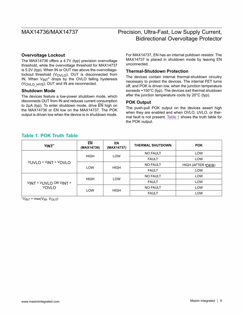
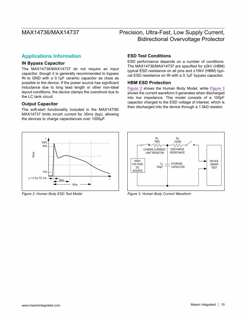
HBM ESD ProtectionFigure 2 shows the Human Body Model, while Figure 3 shows the current waveform it generates when discharged into low impedance. This model consists of a 100pF capacitor charged to the ESD voltage of interest, which is then discharged into the device through a 1.5kΩ resistor.
Figure 2. Human Body ESD Test Model
tr = 0.7ns TO 1ns30ns
60ns
t
100%90%
10%
I PEA
K
I
CHARGE-CURRENT-LIMIT RESISTOR
DISCHARGERESISTANCE
STORAGECAPACITOR
Cs100pF
RC1MΩ
RD1500Ω
HIGH-VOLTAGE
DCSOURCE
DEVICEUNDERTEST
Figure 3. Human Body Current Waveform
MAX14736/MAX14737 Precision, Ultra-Fast, Low Supply Current, Bidirectional Overvoltage Protector
www.maximintegrated.com Maxim Integrated 10
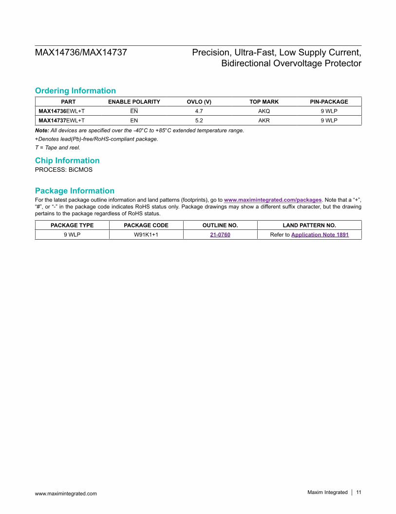
Note: All devices are specified over the -40°C to +85°C extended temperature range.+Denotes lead(Pb)-free/RoHS-compliant package.T = Tape and reel.
PART ENABLE POLARITY OVLO (V) TOP MARK PIN-PACKAGEMAX14736EWL+T EN 4.7 AKQ 9 WLP
MAX14737EWL+T EN 5.2 AKR 9 WLP
PACKAGE TYPE PACKAGE CODE OUTLINE NO. LAND PATTERN NO.9 WLP W91K1+1 21-0760 Refer to Application Note 1891
MAX14736/MAX14737 Precision, Ultra-Fast, Low Supply Current, Bidirectional Overvoltage Protector
www.maximintegrated.com Maxim Integrated 11
Chip InformationPROCESS: BiCMOS
Ordering Information
Package InformationFor the latest package outline information and land patterns (footprints), go to www.maximintegrated.com/packages. Note that a “+”, “#”, or “-” in the package code indicates RoHS status only. Package drawings may show a different suffix character, but the drawing pertains to the package regardless of RoHS status.
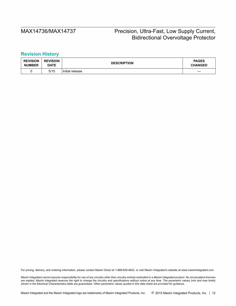
REVISIONNUMBER
REVISIONDATE DESCRIPTION PAGES
CHANGED
0 5/15 Initial release —
Maxim Integrated cannot assume responsibility for use of any circuitry other than circuitry entirely embodied in a Maxim Integrated product. No circuit patent licenses are implied. Maxim Integrated reserves the right to change the circuitry and specifications without notice at any time. The parametric values (min and max limits) shown in the Electrical Characteristics table are guaranteed. Other parametric values quoted in this data sheet are provided for guidance.
Maxim Integrated and the Maxim Integrated logo are trademarks of Maxim Integrated Products, Inc.
MAX14736/MAX14737 Precision, Ultra-Fast, Low Supply Current, Bidirectional Overvoltage Protector
© 2015 Maxim Integrated Products, Inc. 12
Revision History
For pricing, delivery, and ordering information, please contact Maxim Direct at 1-888-629-4642, or visit Maxim Integrated’s website at www.maximintegrated.com.