material and techniques for extended-wavelength and split
TRANSCRIPT

Georgia State University Georgia State University
ScholarWorks @ Georgia State University ScholarWorks @ Georgia State University
Physics and Astronomy Dissertations Department of Physics and Astronomy
Fall 12-10-2018
Material And Techniques For Extended-Wavelength And Split-Off Material And Techniques For Extended-Wavelength And Split-Off
Band Infrared Detectors Band Infrared Detectors
Dilip Chauhan* Georgia State University
Follow this and additional works at: https://scholarworks.gsu.edu/phy_astr_diss
Recommended Citation Recommended Citation Chauhan*, Dilip, "Material And Techniques For Extended-Wavelength And Split-Off Band Infrared Detectors." Dissertation, Georgia State University, 2018. https://scholarworks.gsu.edu/phy_astr_diss/110
This Dissertation is brought to you for free and open access by the Department of Physics and Astronomy at ScholarWorks @ Georgia State University. It has been accepted for inclusion in Physics and Astronomy Dissertations by an authorized administrator of ScholarWorks @ Georgia State University. For more information, please contact [email protected].
MATERIAL AND TECHNIQUES FOR EXTENDED-WAVELENGTH AND SPLIT-OFF
BAND INFRARED DETECTORS
by
DILIP CHAUHAN
Under the Direction of Prof. A.G. Unil Perera, PhD
ABSTRACT
p-GaAs/AlxGa1-xAs heterostructure-based extended-wavelength infrared photodetectors
have been experimentally studied in great detail. Unlike the conventional IR photodetectors with
the wavelength threshold determined by an activation energy (Δ) corresponding to a minimum
energy gap, a novel class of IR photodetectors show an extended-wavelength spectral
photoresponse far beyond the limit set by Δ (given as λt = hc/Δ). p-GaAs/AlxGa1-xAs
heterostructure-based IR photodetectors, with non-zero barrier energy offset between the AlxGa1-
xAs barriers, were used. These IR photodetectors were initially designed to have a conventional
wavelength threshold of ~3 µm, corresponding to Δ ~0.4 eV of p-GaAs/AlxGa1-xAs
heterostructure. However, the extended-wavelength photoresponse was observed up to ~ 60 µm.
The study included a set of devices with varying values of the barrier energy offset. The offset was

found to be necessary for the extended-wavelength mechanism. However, with further increase in
the offset by ~0.13 eV, the extended-wavelength threshold showed a very small variation (~0.002
eV). Instead, increasing the barrier energy offset led to an increased strength of spectral
photoresponse. Similarly, increasing the barrier gradient in another set of devices caused no
significant change in the wavelength threshold. These observations are believed to originate from
build-up of a quasi-equilibrium Fermi level, at a fixed level, irrespective of the variation of the
device parameter. Split-off (S-O) band was found to be the most probable energy level to build-up
a quasi-equilibrium Fermi level as consequence of hot-phonon bottleneck effect. The study of the
dark current characteristics of these IR photodetectors confirmed no compromise in the dark
current due to the presence of the extended-wavelength mechanism of photoresponse. In addition,
from the study of a 2 – 6 µm IR photodetector, based on p-GaAs/AlxGa1-xAs heterostructure,
operating at 0 V, the specific detectivity was found to be enhanced by two orders of magnitude, to
~1.9×10¹¹ Jones, due to a current blocking barrier, although a small compromise in the spectral
responsivity (by a factor of ~1.5) was observed. Furthermore, a 3 – 5 µm band IR photodetector
based on p-InP/InAlAs heterostructure (currently under development), is discussed as an
alternative for the 3 – 5 µm band detection.
INDEX WORDS: III-V semiconductor, IR photodetector, Extended-wavelength mechanism, Hot-
carriers, Hot-phonon bottleneck effect, Mid infrared, Far infrared, Split-off band, Quantum
dots-in-a-well, 3 – 5 µm band IR detector
MATERIAL AND TECHNIQUES FOR WAVELENGTH-EXTENDED AND SPLIT-OFF
BAND INFRARED DETECTORS
by
DILIP CHAUHAN
A Dissertation Submitted in Partial Fulfillment of the Requirements for the Degree of
Doctor of Philosophy
in the College of Arts and Sciences
Georgia State University
2018

Copyright by
Dilip Chauhan
2018
MATERIAL AND TECHNIQUES FOR
EXTENDED-WAVELENGTH AND SPLIT-OFF BAND INFRARED DETECTORS
by
DILIP CHAUHAN
Committee Chair: A. G. Unil Perera
Committee: Vadym Apalkov
Mukesh Dhamala
Douglas Gies
Alexander Kozhanov
Sidong Lei
Electronic Version Approved:
Office of Graduate Studies
College of Arts and Sciences
Georgia State University
December 2018

iv
DEDICATION
To my family and friends for all love and support; and to all nice and great human beings
who helped me succeed!
v
ACKNOWLEDGEMENTS
I would like to take this opportunity to express my sincere gratitude to my supervisor Dr.
Unil Perera for his guidance and support throughout this study. My sincere gratitude is also offered
to my dissertation committee members: Dr. Vadym Apalkov, Dr. Mukesh Dhamala, Dr. Douglas
R. Gies, Dr. Alexander Kozhanov, and Dr. Sidong Lei for their time and effort in reading the
dissertation and valuable suggestions that are vital to improve the quality of this dissertation. I
greatly appreciate the tremendous support from Dr. Sebastian Lepine, Professor and Chair,
Department of Physics and Astronomy. I wish to thank Dr. Edmund H. Linfield, Dr. Lianhe Li,
Dr. Suraj. P. Khanna and Dr. Li Chen at the University of Leeds, Leeds, UK for their extraordinary
collaborative support throughout this study in terms of the device growth, processing, and co-
authoring the journal articles. I would like to express my acknowledgement colleagues, Dr.
Duleepa Pitigala, Dr. Jito Titus, Justin R. Mclaughlin, Dr. Seyoum Wolde, Dimuthu Obysekara,
Sameera Kelum Perera, Dr.Yang‐Feng Lao, Dr. Sanjib Kabi, and Dr. Divya Somvansi and
Hemendre Ghimire for valuable support in course of this study. I wish to thank all the individuals
of the Department of Physics and Astronomy, and friends for their contribution. I also
acknowledge the funding support from the U. S. Army Research Laboratory and the U. S. Army
Research Office under grant number W911NF-15-1-0018 and W911NF-12-2-0035, and the U.S.
National Science Foundation under grant numbers ECCS-1232184. I am also thankful to the
European Community’s Seventh Framework Programme (FP7-IDEAS-ERC) under Grant
agreement No. 247375 ‘TOSCA’, the Wolfson Foundation, and the Royal Society for the support
of Dr. Linfield at the School of Electronic and Electrical Engineering, University of Leeds. I would
like to express my special thanks for a Brains and Behavior Fellowship, Georgia State University,
and a Dissertation Grant 2018, Internal Grants Programs, Georgia State University.
vi
TABLE OF CONTENTS
ACKNOWLEDGEMENTS ............................................................................................ V
LIST OF TABLES ........................................................................................................... X
LIST OF FIGURES ........................................................................................................ XI
LIST OF ABBREVIATIONS ............................................................................... XXVIII
1 P-TYPE GAAS/ALGAAS HETEROSTRUCTURE FOR INFRARED
PHOTODETECTION .................................................................................................................. 1
1.1 Introduction ......................................................................................................... 1
1.2 Objectives of This Study ..................................................................................... 6
1.3 An Overview of p-GaAs/AlGaAs Heterostructure-Based IR Photodetectors 7
1.4 Device Design Principles ................................................................................... 14
1.5 Methods of Optoelectronic Characterizations of IR Detectors ..................... 18
1.6 A Single-Period, Constant Barrier, p-GaAs/AlGaAs Heterostructure-Based
IR Photodetector ..................................................................................................................... 22
1.6.1 Device Parameters and Measurements ........................................................ 22
1.6.2 Results and Discussion ................................................................................. 24
1.7 Summary ............................................................................................................ 36
2 EXTENDED-WAVELENGTH INFRARED PHOTODETECTORS ................. 37
2.1 Introduction ....................................................................................................... 37
2.2 Device Parameters for Barrier Offset and Gradient Variation .................... 39
2.3 Experimental Measurements ........................................................................... 44
2.4 Results and Discussion ...................................................................................... 45
2.4.1 Dark Current and Photoresponse Characteristics of Device 15SP3........... 45
vii
2.4.2 Spectral photoresponse: Non-zero barrier energy offset vs zero barrier
energy offset; and the graded barrier vs the constant barrier ............................................ 51
2.4.1 Spectral photoresponse with barrier energy offset variation ...................... 55
2.4.2 Extended-wavelength photoresponse at zero bias ....................................... 63
2.4.3 Spectral photoresponse with barrier gradient variation .............................. 70
2.4.4 Effect of temperature on the extended wavelength IR photoresponse........ 78
2.5 Future Work ...................................................................................................... 82
2.6 Summary ............................................................................................................ 88
3 DARK CURRENT CHARACTERISTICS OF EXTENDED WAVELENGTH
PHOTODETECTORS ............................................................................................................... 90
3.1 Introduction ....................................................................................................... 90
3.1.1 3D Carrier Drift Model of Dark Current ..................................................... 91
3.2 Results and Discussion ...................................................................................... 93
3.3 Summary .......................................................................................................... 109
4 P-TYPE GAAS/ALGAAS MID-INFRARED PHOTODETECTOR WITH A
CURRENT BLOCKING BARRIER ...................................................................................... 110
4.1 Introduction ..................................................................................................... 110
4.2 Device Parameters and Measurements ......................................................... 111
4.2.1 A 30 period, three terminal, p-GaAs/ AlxGa1-xAs heterostructure with a
current blocking barrier ..................................................................................................... 111
4.3 Results and Discussion .................................................................................... 115
4.3.1 Dark current and the Resistance-area product .......................................... 115
4.3.2 Spectral photoresponse and specific detectivity ......................................... 117
viii
4.3.3 Effect of temperature on the spectral photoresponse ................................ 126
4.3.4 A single-period, two-terminal p-GaAs/ AlxGa1-xAs heterostructure with a
current blocking barrier (Modified CBB device) .............................................................. 128
4.4 Future work on MIR (3 – 5 µm) photodetectors based on p-type InP and
GaInPAs based III-V semiconductor materials ................................................................. 133
4.5 Summary .......................................................................................................... 137
REFERENCES .............................................................................................................. 138
APPENDICES ............................................................................................................... 147
Appendix A ................................................................................................................ 147
Packaging and wire-bonding ................................................................................. 147
Appendix B ................................................................................................................ 149
Electrical Characterization .................................................................................... 149
Appendix C ................................................................................................................ 150
Spectral Characterization ....................................................................................... 150
Appendix D ................................................................................................................ 153
TDIPS fitting by choosing different spectral ranges in the near-threshold region of
extended-wavelength photoresponse .................................................................................. 153
Appendix E ................................................................................................................ 165
Arrhenius Plots and Activation Energy of LH1002 .............................................. 165
TDIPS Fitting of spectral photoresponse LH1002 ................................................ 168
Appendix F ................................................................................................................. 172
Phonon occupation number ................................................................................... 172

ix
x
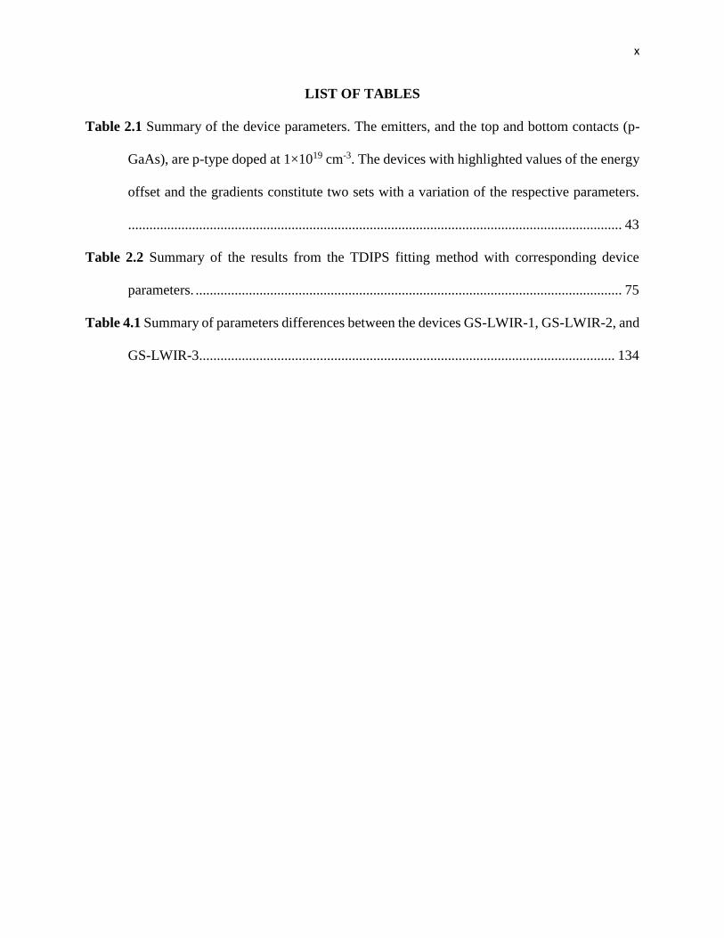
LIST OF TABLES
Table 2.1 Summary of the device parameters. The emitters, and the top and bottom contacts (p-
GaAs), are p-type doped at 1×1019 cm-3. The devices with highlighted values of the energy
offset and the gradients constitute two sets with a variation of the respective parameters.
........................................................................................................................................... 43
Table 2.2 Summary of the results from the TDIPS fitting method with corresponding device
parameters. ........................................................................................................................ 75
Table 4.1 Summary of parameters differences between the devices GS-LWIR-1, GS-LWIR-2, and
GS-LWIR-3..................................................................................................................... 134
xi
LIST OF FIGURES
Figure 1.1 (a) A 3D cartoon representation of multilayered Homojunction/Heterojunction
Interfacial Workfunction Internal Photoemission (HIWIP/HEIWIP) IR photodetector.
Optoelectronic characterizations require top and bottom contact electrodes. IR radiation is
incident from the top, where the top contact (p+-GaAs) is partially etched to open an optical
window. (b) A schematic of valence-band alignment of HIWIP/HEIWIP IR photodetector
under an applied bias. The HIWIP structures utilized p-type doped GaAs absorber/emitter
and undoped GaAs barrier whilst the HEIWIP structures utilized p-type doped GaAs
absorber and undoped AlxGa1-xAs barriers. The interfacial energy gap (Δ) is determined by
the doping level in HIWIP structures. In the HEIWIP structures, Δ is determined primarily
by the Al mole fraction (x) although the doping level also has a contribution. The arrows
depict the photo-excitation of the carriers and internal photoemission, which will undergo
sweep out and collection due to the applied bias. ............................................................... 8
Figure 1.2 (a) A schematic diagram of the equilibrium valence band alignment of a typical
p-GaAs/AlxGa1-xAs heterostructure-based IR photodetector under equilibrium. The active
region of the device is sandwiched between highly p-type doped GaAs top and bottom
contact layers. Δ is the activation energy. (b) A schematic of valence band of GaAs near
k = 0 showing light hole, heavy hole, and split-off bands. The split-off band lies 0.34 eV
below the light hole/heavy hole bands at k = 0. The arrows show some of the possible intra-
valence band (IVB) transitions due to the absorption of IR photons. (c) Operation of the
IR detector under a bias voltage, showing IVB transitions to S-O band due to IR absorption
in the p-GaAs layer and internal photoemission to barrier. .............................................. 11

xii
Figure 1.3 (a) A schematic of valence band alignment of p-GaAs/AlxGa1-xAs heterostructure
corresponding to the layers in the schematic diagram (b) Side view of a processed mesa of
a p-GaAs/AlxGa1-xAs heterostructure-based IR photodetector (LH1002). All p-GaAs
layers- bottom contact (0.5 µm), top contact (0.2 µm) and the emitter (20 nm) are doped at
1×1019 cm-3. (c) Top view optical image of a processed mesa (before wire bonding).
Electrically active area of the mesa is 400 µm × 400 µm, and the optically active area of
the mesa is 260 µm × 260 µm. .......................................................................................... 23
Figure 1.4 Dark current characteristics (measured with Keithley 2635B source meter) of the
p-GaAs/AlxGa1-xAs heterostructure (LH1002) in the applied bias range from -3.0 V to
3.0 V. The current-voltage characteristics show the near-symmetrical in dark current in the
positive and negative applied biases. ................................................................................ 25
Figure 1.5 The Arrhenius plots of for the device LH1002 obtained from the temperature dependent
dark current, in the temperature range of 100 – 200 K. The dashed lines represent the linear
fit to the each of the plots implemented to obtain the slope of the plots. ......................... 27
Figure 1.6 Spectral photoresponse of the p-GaAs/AlxGa1-xAs heterostructure-based IR
photodetector (LH1002) at 78K under positive biases. Intra-valence band transitions to
S-O band (0.34 eV, up to ~ 3.6 µm) contribute to the photoresponse, an in the L-H/H-H
bands (beyond 3.6 µm) contribute to the photoresponse. A small photoresponse is also
observed at 0 V, indicating a slight asymmetry in the heterostructure, possibly originating
from the wafer growth. Inset shows the equilibrium valence band diagram of the device.
........................................................................................................................................... 29
Figure 1.7 Spectral photoresponse of the p-GaAs/AlxGa1-xAs heterostructure-based IR
photodetector (LH1002) at 78K under negative biases. The spectral photoresponse is
xiii
similar to that in the positive biases Inset shows the reduced strength of the photoresponse
at lower applied biases of -0.01 V and -0.015 V in comparison to that at 0 V. This effect
also indicates the presence of a slight asymmetry of the barriers, the effect being canceled
at those small negative biases. .......................................................................................... 30
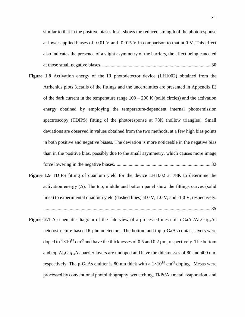
Figure 1.8 Activation energy of the IR photodetector device (LH1002) obtained from the
Arrhenius plots (details of the fittings and the uncertainties are presented in Appendix E)
of the dark current in the temperature range 100 – 200 K (solid circles) and the activation
energy obtained by employing the temperature-dependent internal photoemission
spectroscopy (TDIPS) fitting of the photoresponse at 78K (hollow triangles). Small
deviations are observed in values obtained from the two methods, at a few high bias points
in both positive and negative biases. The deviation is more noticeable in the negative bias
than in the positive bias, possibly due to the small asymmetry, which causes more image
force lowering in the negative biases. ............................................................................... 32
Figure 1.9 TDIPS fitting of quantum yield for the device LH1002 at 78K to determine the
activation energy (Δ). The top, middle and bottom panel show the fittings curves (solid
lines) to experimental quantum yield (dashed lines) at 0 V, 1.0 V, and -1.0 V, respectively.
........................................................................................................................................... 35
Figure 2.1 A schematic diagram of the side view of a processed mesa of p-GaAs/AlxGa1-xAs
heterostructure-based IR photodetectors. The bottom and top p-GaAs contact layers were
doped to 1×1019 cm-3 and have the thicknesses of 0.5 and 0.2 µm, respectively. The bottom
and top AlxGa1-xAs barrier layers are undoped and have the thicknesses of 80 and 400 nm,
respectively. The p-GaAs emitter is 80 nm thick with a 1×1019 cm-3 doping. Mesas were
processed by conventional photolithography, wet etching, Ti/Pt/Au metal evaporation, and
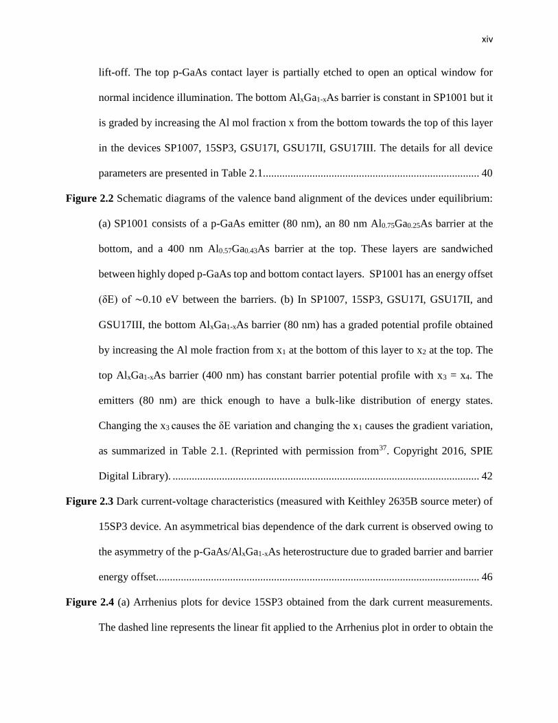
xiv
lift-off. The top p-GaAs contact layer is partially etched to open an optical window for
normal incidence illumination. The bottom AlxGa1-xAs barrier is constant in SP1001 but it
is graded by increasing the Al mol fraction x from the bottom towards the top of this layer
in the devices SP1007, 15SP3, GSU17I, GSU17II, GSU17III. The details for all device
parameters are presented in Table 2.1. .............................................................................. 40
Figure 2.2 Schematic diagrams of the valence band alignment of the devices under equilibrium:
(a) SP1001 consists of a p-GaAs emitter (80 nm), an 80 nm Al0.75Ga0.25As barrier at the
bottom, and a 400 nm Al0.57Ga0.43As barrier at the top. These layers are sandwiched
between highly doped p-GaAs top and bottom contact layers. SP1001 has an energy offset
(δE) of ∼0.10 eV between the barriers. (b) In SP1007, 15SP3, GSU17I, GSU17II, and
GSU17III, the bottom AlxGa1-xAs barrier (80 nm) has a graded potential profile obtained
by increasing the Al mole fraction from x1 at the bottom of this layer to x2 at the top. The
top AlxGa1-xAs barrier (400 nm) has constant barrier potential profile with x3 = x4. The
emitters (80 nm) are thick enough to have a bulk-like distribution of energy states.
Changing the x3 causes the δE variation and changing the x1 causes the gradient variation,
as summarized in Table 2.1. (Reprinted with permission from37. Copyright 2016, SPIE
Digital Library). ................................................................................................................ 42
Figure 2.3 Dark current-voltage characteristics (measured with Keithley 2635B source meter) of
15SP3 device. An asymmetrical bias dependence of the dark current is observed owing to
the asymmetry of the p-GaAs/AlxGa1-xAs heterostructure due to graded barrier and barrier
energy offset...................................................................................................................... 46
Figure 2.4 (a) Arrhenius plots for device 15SP3 obtained from the dark current measurements.
The dashed line represents the linear fit applied to the Arrhenius plot in order to obtain the
xv
slope of the plot. (b) The activation energy of the device 15SP3 obtained from the slope of
Arrhenius plots. The activation energy decreases with the increasing bias voltage due to
image force lowering of the barrier height. The asymmetrical bias dependence is the result
of the asymmetry of the p-GaAs/AlxGa1-xAs heterostructure due to the graded barrier
and energy offset of the barrier. ........................................................................................ 47
Figure 2.5 A comparison of the dark current density of different mesas. Three mesas showing the
dark current curves in solid lines have electrical area of 400 × 400 µm2. The dashed line
shows the dark current density of a mesa with an electrical area of 600 × 600 µm2. ....... 48
Figure 2.6 (a) A schematic representation of operation of an IR detector with barrier gradient and
offset under a negative bias, which causes a barrier bending. Arrows show the possible
transitions to S-O band. (b) Spectral responsivity and specific detectivity of 15SP3
measured at 5.3 K with -1 V bias showing extended-wavelength photoresponse to
60.0 ± 0.4 µm. Ten spectra are plotted on the top of each other. Also, ten spectra of the
background noise level measured by blocking the IR source are also shown, where the dark
solid curve is the average of ten noise spectra. Inset shows the expended view of near
threshold spectra to compare with the average noise level. .............................................. 50
Figure 2.7 The spectral photoresponse of the device LH1002 (with δE = 0 eV) was observed only
in the MIR region, without an extended-wavelength mechanism. However, the device
SP1001 (with δE = 0.10 eV) showed a photoresponse in VLWIR and FIR region with the
wavelength threshold of 50±0.3 µm (determined from TDIPS method, details in Appendix
D), clearly indicating the extended-wavelength mechanism. The device SP1007
(δE = 0.10 eV) with the graded barrier showed a stronger photoresponse in VLWIR and
FIR regime, with the wavelength threshold of 56±0.3 µm. The features associated with the
xvi
AlAs-like and GaAs-like phonons are marked by the arrows. Inset shows the photoresponse
of LH1002, enlarged to show details, clearly showing no extended wavelength mechanism.
........................................................................................................................................... 52
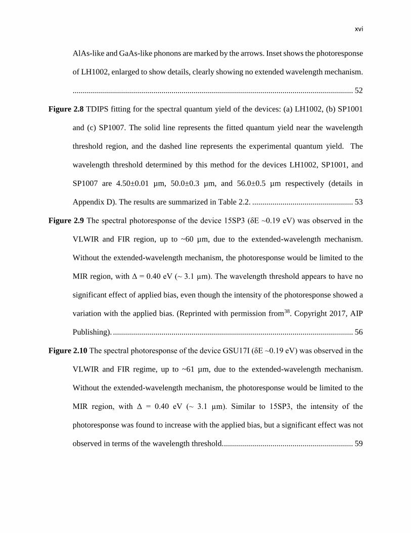
Figure 2.8 TDIPS fitting for the spectral quantum yield of the devices: (a) LH1002, (b) SP1001
and (c) SP1007. The solid line represents the fitted quantum yield near the wavelength
threshold region, and the dashed line represents the experimental quantum yield. The
wavelength threshold determined by this method for the devices LH1002, SP1001, and
SP1007 are 4.50±0.01 µm, 50.0±0.3 µm, and 56.0±0.5 µm respectively (details in
Appendix D). The results are summarized in Table 2.2. .................................................. 53
Figure 2.9 The spectral photoresponse of the device 15SP3 (δE ~0.19 eV) was observed in the
VLWIR and FIR region, up to ~60 µm, due to the extended-wavelength mechanism.
Without the extended-wavelength mechanism, the photoresponse would be limited to the
MIR region, with Δ = 0.40 eV (~ 3.1 µm). The wavelength threshold appears to have no
significant effect of applied bias, even though the intensity of the photoresponse showed a
variation with the applied bias. (Reprinted with permission from38. Copyright 2017, AIP
Publishing). ....................................................................................................................... 56
Figure 2.10 The spectral photoresponse of the device GSU17I (δE ~0.19 eV) was observed in the
VLWIR and FIR regime, up to ~61 µm, due to the extended-wavelength mechanism.
Without the extended-wavelength mechanism, the photoresponse would be limited to the
MIR region, with Δ = 0.40 eV (~ 3.1 µm). Similar to 15SP3, the intensity of the
photoresponse was found to increase with the applied bias, but a significant effect was not
observed in terms of the wavelength threshold. ................................................................ 59
xvii
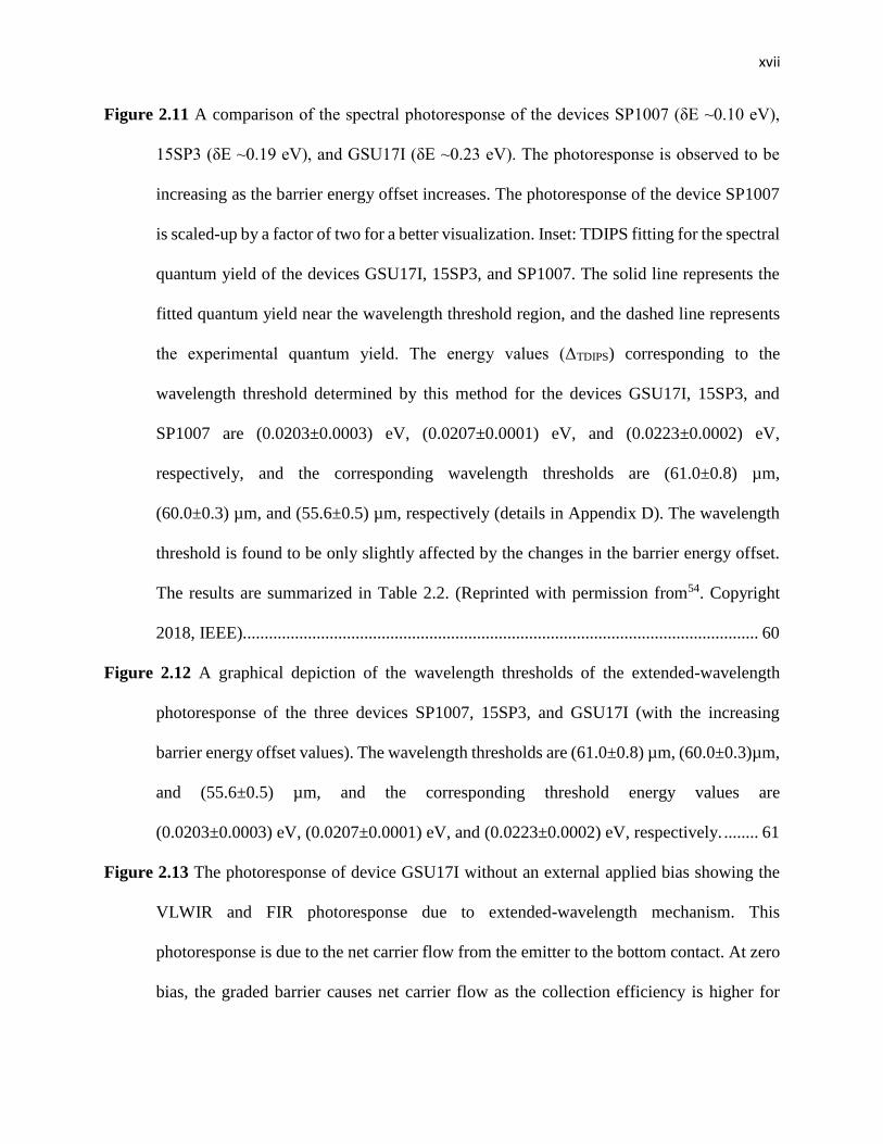
Figure 2.11 A comparison of the spectral photoresponse of the devices SP1007 (δE ~0.10 eV),
15SP3 (δE ~0.19 eV), and GSU17I (δE ~0.23 eV). The photoresponse is observed to be
increasing as the barrier energy offset increases. The photoresponse of the device SP1007
is scaled-up by a factor of two for a better visualization. Inset: TDIPS fitting for the spectral
quantum yield of the devices GSU17I, 15SP3, and SP1007. The solid line represents the
fitted quantum yield near the wavelength threshold region, and the dashed line represents
the experimental quantum yield. The energy values (ΔTDIPS) corresponding to the
wavelength threshold determined by this method for the devices GSU17I, 15SP3, and
SP1007 are (0.0203±0.0003) eV, (0.0207±0.0001) eV, and (0.0223±0.0002) eV,
respectively, and the corresponding wavelength thresholds are (61.0±0.8) µm,
(60.0±0.3) µm, and (55.6±0.5) µm, respectively (details in Appendix D). The wavelength
threshold is found to be only slightly affected by the changes in the barrier energy offset.
The results are summarized in Table 2.2. (Reprinted with permission from54. Copyright
2018, IEEE)....................................................................................................................... 60
Figure 2.12 A graphical depiction of the wavelength thresholds of the extended-wavelength
photoresponse of the three devices SP1007, 15SP3, and GSU17I (with the increasing
barrier energy offset values). The wavelength thresholds are (61.0±0.8) µm, (60.0±0.3)µm,
and (55.6±0.5) µm, and the corresponding threshold energy values are
(0.0203±0.0003) eV, (0.0207±0.0001) eV, and (0.0223±0.0002) eV, respectively. ........ 61
Figure 2.13 The photoresponse of device GSU17I without an external applied bias showing the
VLWIR and FIR photoresponse due to extended-wavelength mechanism. This
photoresponse is due to the net carrier flow from the emitter to the bottom contact. At zero
bias, the graded barrier causes net carrier flow as the collection efficiency is higher for
xviii
carrier flow from the emitter to the bottom contact, compared to that for carrier flow from
bottom contact to the emitter. The inset depicts a schematic band-diagram of the device
showing the barrier maximum position of the graded barrier (zm) near the emitter/graded
barrier interface at 0 V. ..................................................................................................... 64
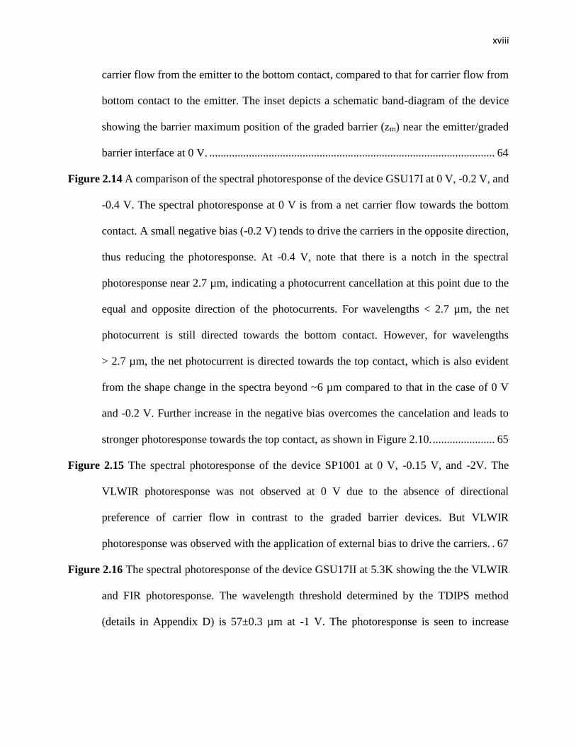
Figure 2.14 A comparison of the spectral photoresponse of the device GSU17I at 0 V, -0.2 V, and
-0.4 V. The spectral photoresponse at 0 V is from a net carrier flow towards the bottom
contact. A small negative bias (-0.2 V) tends to drive the carriers in the opposite direction,
thus reducing the photoresponse. At -0.4 V, note that there is a notch in the spectral
photoresponse near 2.7 µm, indicating a photocurrent cancellation at this point due to the
equal and opposite direction of the photocurrents. For wavelengths < 2.7 µm, the net
photocurrent is still directed towards the bottom contact. However, for wavelengths
> 2.7 µm, the net photocurrent is directed towards the top contact, which is also evident
from the shape change in the spectra beyond ~6 µm compared to that in the case of 0 V
and -0.2 V. Further increase in the negative bias overcomes the cancelation and leads to
stronger photoresponse towards the top contact, as shown in Figure 2.10. ...................... 65
Figure 2.15 The spectral photoresponse of the device SP1001 at 0 V, -0.15 V, and -2V. The
VLWIR photoresponse was not observed at 0 V due to the absence of directional
preference of carrier flow in contrast to the graded barrier devices. But VLWIR
photoresponse was observed with the application of external bias to drive the carriers. . 67
Figure 2.16 The spectral photoresponse of the device GSU17II at 5.3K showing the the VLWIR
and FIR photoresponse. The wavelength threshold determined by the TDIPS method
(details in Appendix D) is 57±0.3 µm at -1 V. The photoresponse is seen to increase

xix
significantly from -0.8 V to -1 V. At -1.2 V, the photoresponse in the MIR and LWIR
regime increases, but remains fairly the same in the rest of the spectrum........................ 72
Figure 2.17 The spectral photoresponse of the device GSU17III showing the VLWIR and FIR
photoresponse. The wavelength threshold determined by the TDIPS method (details in
Appendix D) is 58±0.3 µm at -1 V. The photoresponse is seen to increase significantly
from -0.8 V to -1 V. At -1.2 V, the photoresponse is only slightly higher compared to -1 V
bias voltage. ...................................................................................................................... 73
Figure 2.18 A spectral photoresponse comparison among the devices 15SP3, GSU17II, and
GSU17III, with the barrier gradients 20.6, 28.9, and 37.1 kV/cm respectively. The spectral
photoresponse in the FIR regime can be seen to be slightly being reduced with the with the
increasing barrier gradient, whilst the effect is more noticeable in the MIR and LWIR
regime. Inset: The solid line represents the fitted quantum yield near the wavelength
threshold region, and the dashed line represents the experimental quantum yield. The
energy values (ΔTDIPS) corresponding to the wavelength threshold determined by TDIPS
method (details in Appendix D) are found to be (0.0207±0.0001) eV, (0.0217±0.0001) eV,
and (0.0214±0.0001) eV respectively, and the corresponding wavelength thresholds are
(60.0±0.3) µm, (57.0±0.3) µm, and (58.0±0.3) µm, respectively, for 15SP3, GSU17II, and
GSUIII. The results are summarized in Table 2.2. (Reprinted with permission from54.
Copyright 2018, IEEE). .................................................................................................... 74
Figure 2.19 (a) A comparison of normalized photoresponse in the of 15SP3 (-0.6 V), GSU17II
(-0.8 V), and GSU17III (-0.8 V) showing similar spectral shape in the H-H/L-H regime
(4 – 10 µm). (b) The spectral photoresponse becomes stronger at higher biases of – 1 V for
15SP3 and -1.2 V GSU17II and GSU17III. Similar mechanism is observed in these three
xx
devices, with slightly smaller bias needed for 15SP3 compared to GSU17II and GSU17III.
........................................................................................................................................... 77
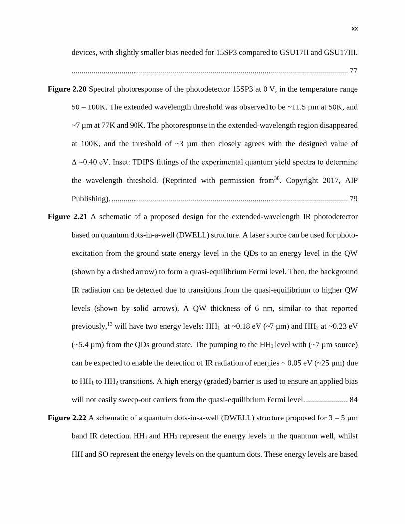
Figure 2.20 Spectral photoresponse of the photodetector 15SP3 at 0 V, in the temperature range
50 – 100K. The extended wavelength threshold was observed to be ~11.5 µm at 50K, and
~7 µm at 77K and 90K. The photoresponse in the extended-wavelength region disappeared
at 100K, and the threshold of ~3 µm then closely agrees with the designed value of
Δ ~0.40 eV. Inset: TDIPS fittings of the experimental quantum yield spectra to determine
the wavelength threshold. (Reprinted with permission from38. Copyright 2017, AIP
Publishing). ....................................................................................................................... 79
Figure 2.21 A schematic of a proposed design for the extended-wavelength IR photodetector
based on quantum dots-in-a-well (DWELL) structure. A laser source can be used for photo-
excitation from the ground state energy level in the QDs to an energy level in the QW
(shown by a dashed arrow) to form a quasi-equilibrium Fermi level. Then, the background
IR radiation can be detected due to transitions from the quasi-equilibrium to higher QW
levels (shown by solid arrows). A QW thickness of 6 nm, similar to that reported
previously,13 will have two energy levels: HH1 at ~0.18 eV (~7 µm) and HH2 at ~0.23 eV
(~5.4 µm) from the QDs ground state. The pumping to the HH1 level with (~7 µm source)
can be expected to enable the detection of IR radiation of energies ~ 0.05 eV (~25 µm) due
to HH1 to HH2 transitions. A high energy (graded) barrier is used to ensure an applied bias
will not easily sweep-out carriers from the quasi-equilibrium Fermi level. ..................... 84
Figure 2.22 A schematic of a quantum dots-in-a-well (DWELL) structure proposed for 3 – 5 µm
band IR detection. HH1 and HH2 represent the energy levels in the quantum well, whilst
HH and SO represent the energy levels on the quantum dots. These energy levels are based
xxi
on the reported experimentally studies.76,77 Excitation from HH to HH2 level can be used
to build up a quasi-equilibrium Fermi level at HH2 level. Then the IR detection in the
3 – 5 µm band may be achieved with an expected peak near 4.3 µm due to the energy
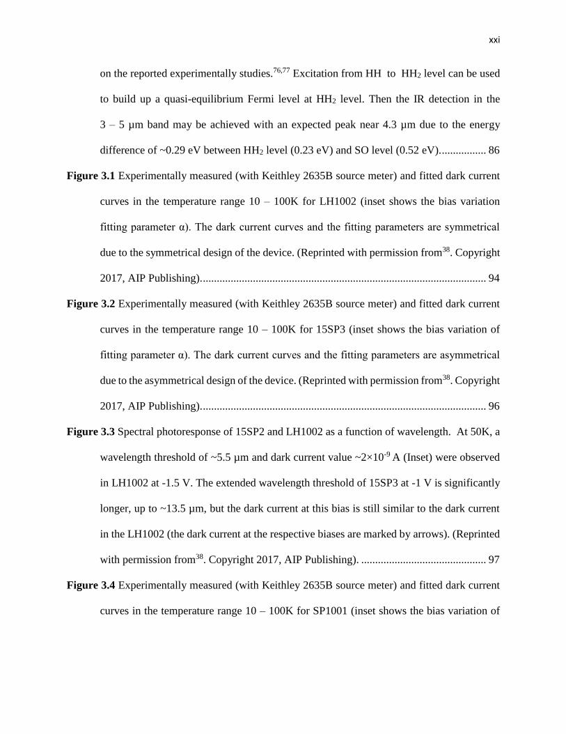
difference of ~0.29 eV between HH2 level (0.23 eV) and SO level (0.52 eV). ................ 86
Figure 3.1 Experimentally measured (with Keithley 2635B source meter) and fitted dark current
curves in the temperature range 10 – 100K for LH1002 (inset shows the bias variation
fitting parameter α). The dark current curves and the fitting parameters are symmetrical
due to the symmetrical design of the device. (Reprinted with permission from38. Copyright
2017, AIP Publishing). ...................................................................................................... 94
Figure 3.2 Experimentally measured (with Keithley 2635B source meter) and fitted dark current
curves in the temperature range 10 – 100K for 15SP3 (inset shows the bias variation of
fitting parameter α). The dark current curves and the fitting parameters are asymmetrical
due to the asymmetrical design of the device. (Reprinted with permission from38. Copyright
2017, AIP Publishing). ...................................................................................................... 96
Figure 3.3 Spectral photoresponse of 15SP2 and LH1002 as a function of wavelength. At 50K, a
wavelength threshold of ~5.5 µm and dark current value ~2×10⁻⁹ A (Inset) were observed
in LH1002 at -1.5 V. The extended wavelength threshold of 15SP3 at -1 V is significantly
longer, up to ~13.5 µm, but the dark current at this bias is still similar to the dark current
in the LH1002 (the dark current at the respective biases are marked by arrows). (Reprinted
with permission from38. Copyright 2017, AIP Publishing). ............................................. 97
Figure 3.4 Experimentally measured (with Keithley 2635B source meter) and fitted dark current
curves in the temperature range 10 – 100K for SP1001 (inset shows the bias variation of

xxii
fitting parameter α). The dark current curves and the fitting parameters are asymmetrical
due to the asymmetrical design of the device. .................................................................. 99
Figure 3.5 (a) Arrhenius plots for device SP1001 obtained from the dark current measurements.
The dashed line represents the linear fit applied to the Arrhenius plot in order to obtain the
slope of the plot. (b) The activation energy of the device SP1001 obtained from the slope
of Arrhenius plots. The activation energy decreases with the increasing bias voltage due to
image force lowering of the barrier height. The asymmetrical bias dependence of activation
energy is the result of the asymmetry of the p-GaAs/AlxGa1-xAs heterostructure due to the
graded barrier and energy offset of the barrier. .............................................................. 100
Figure 3.6 Experimentally measured (with Keithley 2635B source meter) and fitted dark current
curves in the temperature range 10 – 100K for SP1007 (inset shows the bias variation of
fitting parameter α). The dark current curves and the fitting parameters are asymmetrical
due to the asymmetrical design of the device. ................................................................ 101
Figure 3.7 (a) Arrhenius plots for device SP1007 obtained from the dark current measurements.
The dashed line represents the linear fit applied to the Arrhenius plot in order to obtain the
slope of the plot. (b) The activation energy of the device SP1007 obtained from the slope
of Arrhenius plots. The activation energy decreases with the increasing bias voltage due to
image force lowering of the barrier height. The asymmetrical bias dependence of activation
energy is the result of the asymmetry of the p-GaAs/AlxGa1-xAs heterostructure due to the
graded barrier and energy offset of the barrier. .............................................................. 102
Figure 3.8 Experimentally (with Keithley 2400 source meter) measured and fitted dark current
curves in the temperature range 10 – 100K for GSU17I (inset shows the bias variation of
xxiii
fitting parameter α). The dark current curves and the fitting parameters are asymmetrical
due to the asymmetrical design of the device. ................................................................ 103
Figure 3.9 (a) Arrhenius plots for device GSU17I obtained from the dark current measurements.
The dashed line represents the linear fit applied to the Arrhenius plot in order to obtain the
slope of the plot. (b) The activation energy of the device GSU17I obtained from the slope
of Arrhenius plots. The activation energy decreases with the increasing bias voltage due to
image force lowering of the barrier height. The asymmetrical bias dependence of activation
energy is the result of the asymmetry of the p-GaAs/AlxGa1-xAs heterostructure due to the
graded barrier and energy offset of the barrier. .............................................................. 104
Figure 3.10 Experimentally measured (with Keithley 2400 source meter) and fitted dark current
curves in the temperature range 10 – 100K for GSU17II (inset shows the bias variation of
fitting parameter α). The dark current curves and the fitting parameters are asymmetrical
due to the asymmetrical design of the device. ................................................................ 105
Figure 3.11 (a) Arrhenius plots for device GSU17II obtained from the dark current measurements.
The dashed line represents the linear fit applied to the Arrhenius plot in order to obtain the
slope of the plot. (b) The activation energy of the device GSU17II obtained from the slope
of Arrhenius plots. The activation energy decreases with the increasing bias voltage due to
image force lowering of the barrier height. The asymmetrical bias dependence of activation
energy is the result of the asymmetry of the p-GaAs/AlxGa1-xAs heterostructure due to the
graded barrier and energy offset of the barrier. .............................................................. 106
Figure 3.12 Experimentally measured (with Keithley 2400 source meter) and fitted dark current
curves in the temperature range 10 – 100K for GSU17III (inset shows the bias variation of
xxiv
fitting parameter α). The dark current curves and the fitting parameters are asymmetrical
due to the asymmetrical design of the device. ................................................................ 107
Figure 3.13 (a) Arrhenius plots for device GSU17III obtained from the dark current
measurements. The dashed line represents the linear fit applied to the Arrhenius plot in
order to obtain the slope of the plot. (b) The activation energy of the device GSU17III
obtained from the slope of Arrhenius plots. The activation energy decreases with the
increasing bias voltage due to image force lowering of the barrier height. The asymmetrical
bias dependence of activation energy is the result of the asymmetry of the p-GaAs/AlxGa1-
xAs heterostructure due to the graded barrier and energy offset of the barrier. .............. 108
Figure 4.1 (a) Schematic side view of the of the p-GaAs/ AlxGa1-xAs heterostructure, including
the current blocking barrier (CBB). The top (T) and bottom (B) contacts are used to
measure with the CBB, and the middle (M) and bottom contacts can be used to measure
the same mesa without it. (b) Top view optical image of the detector mesa showing the
lateral dimensions of the top contact (400 µm × 400 µm) and middle contact (570 µm ×
570 µm), with the optical window (260 µm × 260 µm) at the center. (Reprinted with
permission from59. Copyright 2016, AIP Publishing). ................................................... 112
Figure 4.2 (a) Schematic of the valence band alignment of the heterostructure under equilibrium
showing the connections with the CBB and without the CBB. The AlxGa1-xAs barriers are
graded by tuning the Al mole fraction, x. (b) A schematic of the valence band of the GaAs
near k = 0, showing some of the possible hole transitions from light hole/heavy hole to
split-off bands, and also from the heavy hole to light hole band. The emitters are thick
enough for bulk-like distribution of the density of states of carriers. (Reprinted with
permission from59. Copyright 2016, AIP Publishing). ................................................... 113
xxv
Figure 4.3 The dark current density of the detector with CBB (T-B) is five orders of magnitude
smaller at low bias, than without the CBB (M-B). The difference becomes smaller as the
bias increases. The dark current across the top and middle (T-M) contacts is similar to that
across T-B contacts in the low bias region. (Reprinted with permission from59. Copyright
2016, AIP Publishing). .................................................................................................... 116
Figure 4.4 Comparison of the responsivity of the detector showing that the responsivity with the
CBB is ~ 1.5 times smaller at zero bias, than without the CBB. For the wavelengths
≤ 2 µm, the energy of photoexcited carriers (≥ 0.6 eV) is much larger than the CBB height
(~0.55 eV) and is a possible reason that the photoresponse is nearly the same in both cases
for wavelengths ≤ 2 µm. (Reprinted with permission from59. Copyright 2016, AIP
Publishing). ..................................................................................................................... 118
Figure 4.5 Specific detectivity D* showing two orders of magnitude higher detectivity with the
CBB, owing to the higher R0A despite a small reduction in the photoresponse. (Reprinted
with permission from59. Copyright 2016, AIP Publishing). ........................................... 119
Figure 4.6 (a) The spectral photoresponse measure with the applied bias increasing with the step
size of 0.2 V, across the middle and bottom contacts, that is, without the CBB. (b) The
spectral photoresponse measured across top and bottom contacts, that is, with the CBB.
The photoresponse is seen increasing with the application of bias, the effect being slightly
stronger in the case of without the CBB. ........................................................................ 121
Figure 4.7 (a) Peak spectral responsivity (at 2.7 µm) from the measurements with the CBB (top-
bottom) and without the CBB (middle-bottom). The applied biases caused a slight
increment in the photoresponse, the effect is more noticeable in the measurement without
the CBB. (b) The specific detectivity (D*) was observed to be maximum at zero bias and
xxvi
it decreased with the application of bias, thus making the photovoltaic operation more
attractive over the photoconductive operation. ............................................................... 122
Figure 4.8 The photoresponse measured across top and middle contact, was disabled by the optical
filter with λCO = 2.4 µm. (Reprinted with permission from59. Copyright 2016, AIP
Publishing). ..................................................................................................................... 124
Figure 4.9 Optical filters of cut-on wavelengths of λCO = 2.4 µm and 4.5 µm did not show any
effect on the photoresponse in the spectral range longer than λCO, in the measurements –
(a) with the CBB, and (b) without the CBB.................................................................... 125
Figure 4.10 The spectral photoresponse at temperatures 77K, 120 K, 130 K, 140 K, and 200 K.
The photoresponse is seen to be reduced by an order of magnitude from 77 K to 120 K and
becomes more at 130 K. At 140 K, the photoresponse beyond ~2.5 µm is seen to be
deteriorated more dramatically, showing only a very weak and noisy signal in this spectral
range. The spectral photoresponse up to ~2.5 µm was observed at 200 K. .................... 127
Figure 4.11 (a) Schematic of the valence band alignment of modified CBB device under
equilibrium. In comparison to the Figure 4.2 (a), the 500 nm thick middle contact layer is
replaced by a 20 nm buffer layer in the modified CBB device. The Al mole fraction of the
graded barrier is slightly higher, graded from x = 0.12 to 0.53. A single-period
emitter/barrier is used instead of 30-periods, thus an average applied electric field
corresponding to a particular bias voltage will be ~30 times higher in the modified CBB
device compared to the previous CBB device. Due to the absence of middle contact, the
measurements are carried out across the top-bottom contacts only, that is, with the CBB.
(b) Dark current density of the modified CBB device. ................................................... 129
xxvii
Figure 4.12 (a) The spectral photoresponse of the modified CBB device at 0 V, measured at the
temperatures 77 K, 90 K, 100K, and 120 K, showing no significant change in the
photoresponse signal although a slight increment was observed with the temperature
increasing from 77 K to 120 K. (b) Above 120 K, the photoresponse was observed to be
reduced with the increasing temperature, as observed previously in Figure 4.10. An
operating temperature of 150 K is observed, before the spectral photoresponse beyond
~2.5 µm disappeared. At 200 K, the spectral photoresponse is limited to ~2.5 µm, similar
to previously observed result. ......................................................................................... 130
Figure 4.13 A comparison between the CBB device and the modified CBB device in terms of (a)
spectral photoresponse, and (b) specific detectivity (D*) at 120 K, 0 V. The modified CBB
device is seen to have a higher responsivity and the specific detectivity. ...................... 132
Figure 4.14 Schematic of the p-InP/InAlAs heterostructure for 3-5 µm IR detection. Three
samples are designed: GS-LWIR-1 with p-InP doping 3.0×1018 cm-3 and emitter thickness
T = 20 nm; GS-LWIR-2 with p-InP doping 3.0×1018 cm-3 and emitter thickness T = 80 nm;
and GS-LWIR-3 with p-InP doping 8.0×1018 cm-3 and emitter thickness T = 80 nm. ... 134
Figure 4.15 Simulated spectral photoresponse of the p-InP/InAlAs heterostructure IR
photodetector for 3-5 µm (FWHM) detection. ............................................................... 135

xxviii
LIST OF ABBREVIATIONS
µm – micro-meter
0D, 1D, 2D, and 3D – Zero-, One-, Two-, Three- Dimensional
AlAs – Aluminum Arsenide
AlP – Aluminum Phosphide
AlxGa1-xAs - Aluminum Gallium Arsenide, x is Al mole fraction
B – bottom
CBB – current blocking barrier
CBIRD - complementary barrier infrared detectors
D* - Specific Detectivity
DC or dc - Direct Current
DUT – Device Under Test
DWELL - Quantum Dots-in-Well Infrared Photodetector
e – Electronic charge
eV - Electron Volts
FPA – Focal Plane Array
FIR – Far infrared
FTIR - Fourier Transform Infrared
FWHM – Full Width Half Maximum
GaAs - Gallium Arsenide
GaInAsP – Gallium Indium Arsenide Phosphide
GaP – Gallium Phosphide
GaSb – Gallium Antimonide

xxix
h – Planck constant
HEIWIP - Heterojunction Interfacial Work Function Internal Photoemission
HgCdTe – Mercury Cadmium Telluride
H-H - Heavy Hole
HIWIP - Homojunction Interfacial Workfunction Internal Photoemission
InAlAs – Indium Aluminum Arsenide
InAs - Indium Arsenide
InGaAs - Indium Gallium Arsenide
InP – Indium Phosphide
IR – Infrared
IVB – intra-valence band
I-V-T - Current-Voltage-Temperature
k – Reciprocal lattice wavevector of GaAs
L-H - Light Hole
LO – Longitudinal Optic
LWIR – Long Wavelength Infrared
M – middle
MBE - Molecular Beam Epitaxy
MCT – Mercury Cadmium Telluride
MIR - Mid- Infrared
mm – millimeter
MWIR - medium-wavelength infrared
NIR - Near infrared

xxx
nm – nanometer
n-type – free electron charge carrier
PbIbN - p-type-intrinsic-n-type
p-Type – free Hole charge carrier
QDIPs - Quantum Dot Infrared Photodetectors
QDs - Quantum Dots
QWIPs - Quantum Well Infrared Photodetectors
R0A - resistance-area product
S-O - Spin-Orbit Split-off band
subMM – submillimeter
SWIR – short-wavelength infrared
T – top
T2SL - type II InAs/GaSb superlattice
TDIPS - temperature-dependent internal photoemission spectroscopy
THz – Terahertz
Ti/Pt/Au – Titanium/Platinum/Gold
TO - transverse-optical
VB - Valence Band
VLWIR - very-long wavelength infrared
λCO - cut-on wavelength of optical filter
λc - wavelength corresponding to full width at half maximum
λt - wavelength threshold

xxxi
1
1 P-TYPE GAAS/ALGAAS HETEROSTRUCTURE FOR INFRARED
PHOTODETECTION
1.1 Introduction
Infrared (IR) radiation covers a range in the electromagnetic radiation with the wavelengths
longer than the visible, but shorter than millimeter waves. More specifically, electromagnetic
radiation in the wavelength range of 0.78 µm to 1000 µm (or 1 mm) constitutes IR radiation, even
though this is not a strict classification. Being invisible to the human eye, IR radiation was
unknown to humans until its discovery by Frederick William Herschel in 1800 while studying the
spectrum of sunlight with a prism and measuring the temperature of each color.1 Herschel found
that the highest temperature change on a thermometer was caused by an invisible spectrum of light
just beyond the red, to be named as “infra-red”.
The IR radiation band is subdivided to many spectral regimes, even though a unique
subdivision does not exist. The most common subdivision includes seven spectral regimes,2
namely near IR (NIR, 0.78 – 1 µm), short-wavelength IR (SWIR, 1 – 3 µm), medium-wavelength
IR (MWIR, 3 – 6 µm), long-wavelength IR (LWIR, 6 – 15 µm), very-long wavelength IR
(VLWIR, 15 – 30 µm), far IR (FIR, 30 - 100 µm), and submillimeter (subMM, 100 – 1000 µm).
Furthermore, the IR radiation in the 30 – 300 µm spectral regime is also referred to as the terahertz
(THz) radiation in terms of the radiation frequency (10 – 1 THz). Furthermore, the atmospheric
transmission windows of 3 – 5 µm and 8 – 14 µm are also commonly referred to as MIR and LWIR
bands, respectively.
2
Vibrating charged particles, including atoms, generate electromagnetic radiation.
Naturally, all objects above absolute zero temperature emit IR radiation. The relationship between
wavelength at the peak intensity of the emission spectrum ( p ) and the temperature (T ) of the
radiating source (ideally a blackbody) is given by 2898=Tp µmK. Accordingly, a human body
radiates with a p ~ 9.5 µm (LWIR), the sun with p ~ 0.5 µm (visible), and a passenger jet exhaust
with p ~ 4 µm (T ~ 700 K). Detection of IR radiation means the detection of an object, the source
of the IR radiation. IR detectors and imaging systems enable one to see the objects even in the
absence of visible light. IR imaging systems can easily recognize a camouflage object in the visible
spectrum. Furthermore, Rayleigh-type (4− ) scattering is much smaller in the IR spectrum
compared to that in the visible spectrum, rendering much better visibility with IR imaging systems
through dust, smoke, and cloud.2
These fundamental characteristics of the IR radiation have found a wide range of
applications3 – including military, civilian and scientific research. Historically, research and
development of IR detectors was driven primarily due to military interest, and still is the case as
IR imaging systems are becoming a “differentiating key-factor of military superiority”.3 IR
imaging systems are employed with applications in ground-based, air-based, and space based
surveillance and targeting systems, such as tank-sight systems, anti-tank missiles, and air–air
missiles.
Although military applications are still the major interest, the applications of the IR
detectors and imaging systems are growing in recent decades in diverse areas. These areas include
industrial energy loss monitoring, scientific researches such as IR astronomy and global
monitoring of environmental pollution and climate change2, firefighting, search and rescue2,
3
security surveillance2, driving and navigation,2 and medical imaging and diagnostics.4,5 The
demands for such a diverse group of applications need IR imaging systems with unique
operational characteristics such as speed, resolution, power requirement, cost, size, operational
temperature and so on. For example, IR astronomy requires large array size6 without a stringent
cost restriction, whereas IR security cameras can be still useful with a small array size but a low
cost is critical for large scale applications. In fact, the requirements of the new generation of IR
imaging systems are not just the high-performance, large-format cooled imagers, but also
medium- to high-performance uncooled imagers, and very low cost, expendable uncooled
imagers.7 In addition, multispectral detection is crucial for increasing the target identification
range, and also to overcome the problem of contrast washout between the target and background.3
A functional near-IR spectroscopy (fNIRS, 700 -1000 nm) of brain tissue temperature was also
studied theoretically for non-invasive brain imaging owing to the difference of the blood oxygen
level dependent (BOLD) absorption of NIR (0.6 – 1.1 µm) radiation.8-12 Further studies are
reported recently in fNIRS based cortical signal analysis,13 hemodynamic response as measured
by fNIRS studies in newborns14, differential path-length factor's effect on the characterization of
the brain's hemodynamic response in the fNIRS method.15 Moreover, progress being made in
wireless and wearable fNIRS systems is expected to be increasingly useful in neuroimaging in
naturalistic environments and social cognitive neuroscience.16 Potential biomedical application of
MIR and LWIR region (IR spectral fingerprint region17, 5 – 10 µm or 1000 – 2000 cm-1) can help
us understand disease associated alteration in major biomolecules such as carbohydrates, nucleic
acids proteins and lipids. Our colitis and cancer studies showed that serum changes in MIR and in
the attenuated total internal reflection spectrum18-20 reflect changes in the serum due to illness.
Since one type of cancer studied was also a subcutaneous tumor20, a brain tumor is also likely to

4
demonstrate serum changes. Thus, MIR and LWIR imaging systems can be used in the diagnostics
of brain tumors. Therefore, MIR and LWIR imaging systems hold promise in the diagnostics of
brain tumors, and further development of MIR detectors should be undertaken with this aim in
mind.
Development of fNIR spectroscopy for brain imaging primarily relies on the detection of
BOLD NIR signal from the brain tissues. IR absorption properties of water is also a critical factor
that can have its effect through absorption in the tissue. A careful observation of the differences
on the BOLD IR absorption spectrum8 in the range of 0.6 to 1.1 µm reveals that a maximum
difference in the BOLD absorption is in the wavelengths shorter than 0.7 µm, where the
deoxyhemoglobin (deoxyHb) absorption is higher than the oxyhemoblobin (oxyHb) absorption.
Absorption by water is also extremely small in this spectral region. However, this spectral range
is in the visible region, hence ambient light can easily interfere with the BOLD signal from brain
tissues. The difference in the BOLD absorption becomes smaller at further longer wavelengths
and oxyHb and deoxyHb signals are same at 0.8 µm. Then the oxyHb absorption becomes stronger
than deoxyHb absorption at wavelength range of 0.8 to 1.1 µm. However, absorption by water also
becomes stronger at this wavelength range, the strongest peak being near 0.98 µm. Even a small
absorption by water amounts to be significant given the considerable tissue thickness in the path
of BOLD signal to the detector. The intensity of the signal weakens exponentially through the
tissue due to water absorption according to Beer-Lambart law. This means a search for another
spectral band where the IR transmission through water is very high. One of such spectral band is
3 – 5 µm with an excellent IR transmission through water21, with a peak transmission near 100%
at 3.8 µm. Therefore, 3 – 5 µm spectral band is interesting for non-invasive optical imaging of
brain using BOLD signal detection techniques. However, absorption properties of deoxy and

5
oxyHb is needed to be studied in this spectral band in order to fully assess the potential of non-
invasive brain imaging in 3 – 5 µm IR band.
Several material systems and techniques have been explored for IR detector and imaging
systems. Historically, mercury-cadmium-telluride (HgCdTe or MCT) based IR detectors are the
most widely used for high-performance applications (e.g., military)22. However, widespread
applications of these detectors have been impeded due to the fundamental material problems. The
HgCdTe material system is marred by high defect density related to growth due to the weak Hg-
Te bond23. This is a serious technological problem for the mass production of HgCdTe large sized
Focal Plane Arrays (FPA), and to achieve high FPA pixel uniformity and yield. On the other hand,
Quantum Well IR Photodetectors (QWIPs) based on GaAs/AlGaAs material system are
considered, mostly LWIR spectral regime for high-performance applications. The industrial
infrastructure in III–V materials/device growth, processing, and packaging brought about by the
utility of GaAs based devices in the telecommunications industry gives QWIPs a potential
advantage in producibility and cost22. However, QWIPs are not sensitive to normal incident light
due to orthogonality between polarization vector of the incident photons and optical transition
dipole moment24, therefore a light coupling structures are required for a 45° angle incidence of
light which adds cost and complexity. In addition, a low operating temperature is typically required
due to fundamental limitations associated with intersubband transitions.22 Studies of Quantum Dot
IR Photodetectors (QDIPs) are also making progress towards the development of IR detectors.22,25

6
1.2 Objectives of This Study
The primary objective of this work is to study the recently demonstrated extended-
wavelength IR photodetectors based on p-GaAs/AlGaAs heterostructures. The extended
wavelength IR photodetectors are novel class of photodetectors showing spectral photoresponse
far beyond the conventional limit of
=hc
t , where is the minimum energy that determines the
wavelength threshold (λt) of the photoresponse. Since the dark current in the extended-wavelength
IR photodetectors is still limited by as in the conventional photodetectors, the extended-
wavelength mechanism offers a new avenue for the design and development of the IR
photodetectors. The device architecture used to demonstrate the extended-wavelength
photoresponse utilized an offset (𝛿𝐸) between the energy barriers in the p-GaAs/AlGaAs
heterostructure, and a reference photodetector without the offset did not show the extended-
wavelength mechanism. Thus, it is important have a deeper understanding of the mechanism by
studying the effect of the device parameters such as the offset and gradient of the barrier. This
study is intended to carry out a detailed investigation on the extended-wavelength mechanism so
that the findings from this study can set path forward to the development of IR photodetectors by
utilizing the extended-wavelength mechanism in quantum nanostructures such as quantum dots-
in-a-well (DWELL) IR photodetectors, and possibly achieve higher operating temperatures. The
study of the dark current characteristics of the extended-wavelength photodetector along with the
reference photodetector is intended to shed light on the fact that the dark current of the extended-
wavelength photoresponse still offers the advantage that the dark current is limited by as in the
case of conventional photodetection whilst the spectral photoresponse is observed far beyond the
conventional limit of .
7
The other objective of this study is to explore possible ways to improve the performance
of the p-GaAs/AlGaAs heterostructure-based split-off band MIR detectors. The effect of
implementation of a current blocking barrier in order to improve the performance in MIR detection
will be studied. By using the current blocking barrier on a 30-period p-GaAs/AlGaAs
heterostructure with graded barrier, its effect will be investigated with and without the current
blocking barrier on the same device. An operation at zero bias is achieved due to the graded
AlGaAs barriers implemented in the heterostructure. The zero bias operation enabled by the graded
barrier will be compared with the biased operation to find and optimum operating condition. Long
pass optical filters will also be used in order to understand the fact that the current blocking barrier
will not affect the spectral range of the photoresponse. In addition to split-off band IR absorber
for MIR detection in p-GaAs absorber, other material options such as p-InP will also be explored
in order to develop p-InP/InGaAlAs heterostructure-based 3 – 5 µm band IR photodetectors based
on the split-off band detection mechanism.
1.3 An Overview of p-GaAs/AlGaAs Heterostructure-Based IR Photodetectors
The III–V material based heterostructures such as p-GaAs/AlxGa1-xAs heterostructure-
based IR Photodetectors would have the same advantages of the QWIPs in terms of growth,
processing, and packaging and high yield and pixel uniformity, with additional advantages of
sensitivity to normal incidence light, high operating temperature, and tunability to a wide spectral
range. Historically, p-GaAs layers were used as IR absorber/emitter in the development
Homojunction Interfacial Workfunction Internal Photoemission26,27 (HIWIP) IR photodetectors
for FIR detection. A multilayered emitter/barrier structure between the top and bottom contacts is
depicted in Figure 1 (a). Normal incidence of IR radiation through top contact generates photo-
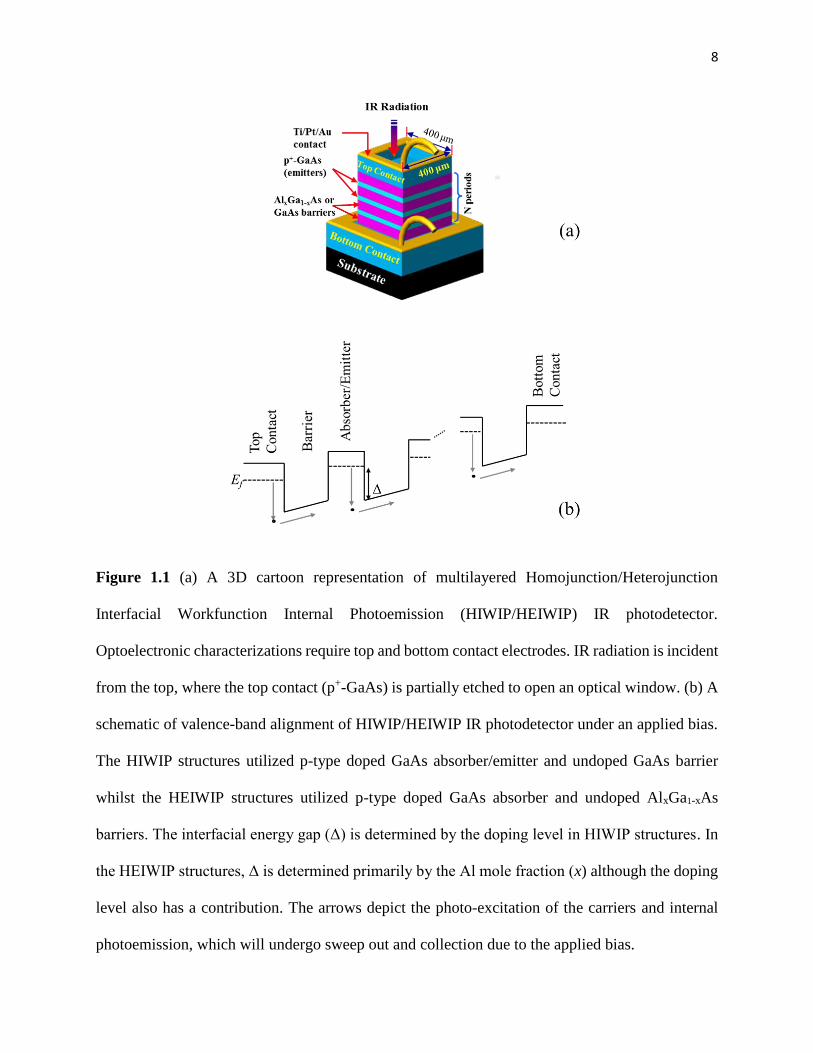
8
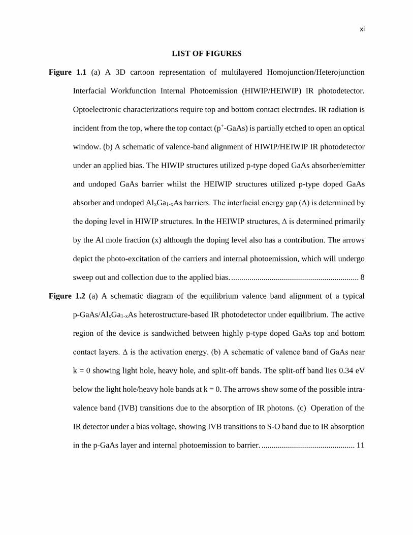
Figure 1.1 (a) A 3D cartoon representation of multilayered Homojunction/Heterojunction
Interfacial Workfunction Internal Photoemission (HIWIP/HEIWIP) IR photodetector.
Optoelectronic characterizations require top and bottom contact electrodes. IR radiation is incident
from the top, where the top contact (p+-GaAs) is partially etched to open an optical window. (b) A
schematic of valence-band alignment of HIWIP/HEIWIP IR photodetector under an applied bias.
The HIWIP structures utilized p-type doped GaAs absorber/emitter and undoped GaAs barrier
whilst the HEIWIP structures utilized p-type doped GaAs absorber and undoped AlxGa1-xAs
barriers. The interfacial energy gap (Δ) is determined by the doping level in HIWIP structures. In
the HEIWIP structures, Δ is determined primarily by the Al mole fraction (x) although the doping
level also has a contribution. The arrows depict the photo-excitation of the carriers and internal
photoemission, which will undergo sweep out and collection due to the applied bias.
9
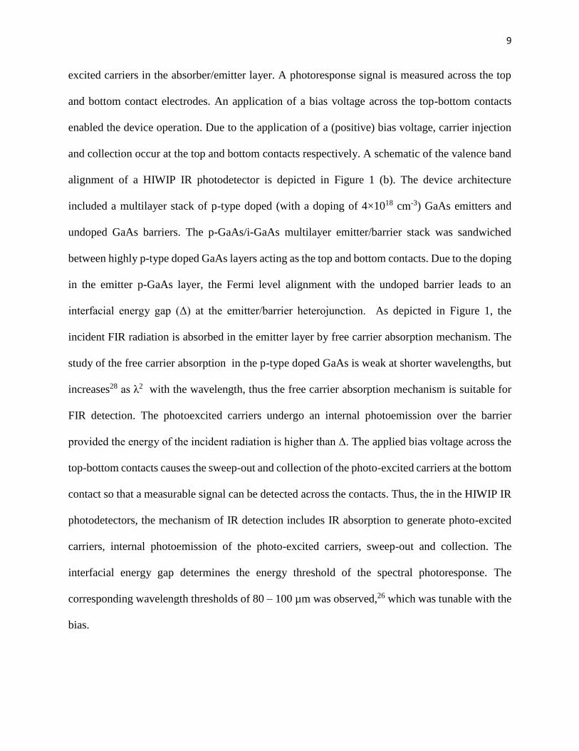
excited carriers in the absorber/emitter layer. A photoresponse signal is measured across the top
and bottom contact electrodes. An application of a bias voltage across the top-bottom contacts
enabled the device operation. Due to the application of a (positive) bias voltage, carrier injection
and collection occur at the top and bottom contacts respectively. A schematic of the valence band
alignment of a HIWIP IR photodetector is depicted in Figure 1 (b). The device architecture
included a multilayer stack of p-type doped (with a doping of 4×1018 cm-3) GaAs emitters and
undoped GaAs barriers. The p-GaAs/i-GaAs multilayer emitter/barrier stack was sandwiched
between highly p-type doped GaAs layers acting as the top and bottom contacts. Due to the doping
in the emitter p-GaAs layer, the Fermi level alignment with the undoped barrier leads to an
interfacial energy gap (Δ) at the emitter/barrier heterojunction. As depicted in Figure 1, the
incident FIR radiation is absorbed in the emitter layer by free carrier absorption mechanism. The
study of the free carrier absorption in the p-type doped GaAs is weak at shorter wavelengths, but
increases28 as λ2 with the wavelength, thus the free carrier absorption mechanism is suitable for
FIR detection. The photoexcited carriers undergo an internal photoemission over the barrier
provided the energy of the incident radiation is higher than Δ. The applied bias voltage across the
top-bottom contacts causes the sweep-out and collection of the photo-excited carriers at the bottom
contact so that a measurable signal can be detected across the contacts. Thus, the in the HIWIP IR
photodetectors, the mechanism of IR detection includes IR absorption to generate photo-excited
carriers, internal photoemission of the photo-excited carriers, sweep-out and collection. The
interfacial energy gap determines the energy threshold of the spectral photoresponse. The
corresponding wavelength thresholds of 80 – 100 µm was observed,26 which was tunable with the
bias.
10
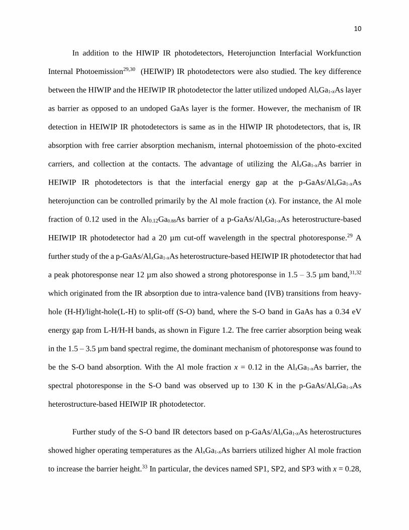
In addition to the HIWIP IR photodetectors, Heterojunction Interfacial Workfunction
Internal Photoemission29,30 (HEIWIP) IR photodetectors were also studied. The key difference
between the HIWIP and the HEIWIP IR photodetector the latter utilized undoped AlxGa1-xAs layer
as barrier as opposed to an undoped GaAs layer is the former. However, the mechanism of IR
detection in HEIWIP IR photodetectors is same as in the HIWIP IR photodetectors, that is, IR
absorption with free carrier absorption mechanism, internal photoemission of the photo-excited
carriers, and collection at the contacts. The advantage of utilizing the AlxGa1-xAs barrier in
HEIWIP IR photodetectors is that the interfacial energy gap at the p-GaAs/AlxGa1-xAs
heterojunction can be controlled primarily by the Al mole fraction (x). For instance, the Al mole
fraction of 0.12 used in the Al0.12Ga0.88As barrier of a p-GaAs/AlxGa1-xAs heterostructure-based
HEIWIP IR photodetector had a 20 µm cut-off wavelength in the spectral photoresponse.29 A
further study of the a p-GaAs/AlxGa1-xAs heterostructure-based HEIWIP IR photodetector that had
a peak photoresponse near 12 µm also showed a strong photoresponse in 1.5 – 3.5 µm band,31,32
which originated from the IR absorption due to intra-valence band (IVB) transitions from heavy-
hole (H-H)/light-hole(L-H) to split-off (S-O) band, where the S-O band in GaAs has a 0.34 eV
energy gap from L-H/H-H bands, as shown in Figure 1.2. The free carrier absorption being weak
in the 1.5 – 3.5 µm band spectral regime, the dominant mechanism of photoresponse was found to
be the S-O band absorption. With the Al mole fraction x = 0.12 in the AlxGa1-xAs barrier, the
spectral photoresponse in the S-O band was observed up to 130 K in the p-GaAs/AlxGa1-xAs
heterostructure-based HEIWIP IR photodetector.
Further study of the S-O band IR detectors based on p-GaAs/AlxGa1-xAs heterostructures
showed higher operating temperatures as the AlxGa1-xAs barriers utilized higher Al mole fraction
to increase the barrier height.33 In particular, the devices named SP1, SP2, and SP3 with x = 0.28,

11
Figure 1.2 (a) A schematic diagram of the equilibrium valence band alignment of a typical
p-GaAs/AlxGa1-xAs heterostructure-based IR photodetector under equilibrium. The active region
of the device is sandwiched between highly p-type doped GaAs top and bottom contact layers. Δ
is the activation energy. (b) A schematic of valence band of GaAs near k = 0 showing light hole,
heavy hole, and split-off bands. The split-off band lies 0.34 eV below the light hole/heavy hole
bands at k = 0. The arrows show some of the possible intra-valence band (IVB) transitions due to
the absorption of IR photons. (c) Operation of the IR detector under a bias voltage, showing IVB
transitions to S-O band due to IR absorption in the p-GaAs layer and internal photoemission to
barrier.

12
0.37, and 0.57, respectively, showed the operating temperatures of 140, 190 and 300 K
respectively.33 Furthermore, a device modeling study34 of S-O band IR detector was carried out
in order to find optimized conditions for its performance improvement. The study suggested two
important device architecture modifications in order to improve the device performance. One of
the suggestions was to include an offset (𝛿𝐸) between the energy barriers so that the low energy
barrier towards the collector side would enhance the collection. The other suggestion was to
include a graded barrier on the injector side so that the carrier trapping would be reduced and the
injection of the carriers to the absorber/emitter would be improved.
The study of the S-O band detector devices with the barrier offset (𝛿𝐸) and a graded barrier
showed an unprecedented result in terms of the spectral range of the photoresponse: a
photoresponse that is far beyond the spectral limit35 of = /hct
. In particular, the p-
GaAs/AlxGa1-xAs heterostructures-based IR detector designed with a Δ ~ 0.40 eV (~ 3.1 µm) for
S-O (MIR) band detection also demonstrated a FIR spectral photoresponse36 up to ~55 µm, which
is far beyond the spectral limit of Δ of the heterostructure. Furthermore, this mechanism of
photoresponse beyond the spectral limit had interesting properties that a spectrum of high energy
IR radiation with wavelengths shorter than ~4.5 µm was necessary in order to observe the FIR
spectral photoresponse.36 This observation was confirmed by using long-pass optical filters to
block the incoming IR radiation in the spectra of wavelengths shorter than 4.5 µm that led to the
disappearance of the FIR photoresponse. With the optical filter still in the light path, the FIR
photoresponse was recovered by using an external IR source to enable the S-O band
photoexcitation in the detector.36 Furthermore, a reference p-GaAs/AlxGa1-xAs heterostructures-
based IR detector without an offset did not show the extended-wavelength photoresponse.36
Therefore, a detailed study of the extended-wavelength photoresponse mechanism, including the
13
effect of variations of the parameters such as the barrier offset and gradient is necessary to achieve
the objectives outlined in the previous section.
This study will investigate in detail the extended-wavelength photoresponse mechanism.
Here, my work is focused on the extensive experimental study of the extended-wavelength IR
photodetectors, which will be presented in Chapters 2 and 3.
Although the photoresponse of a single-period p-GaAs/AlxGa1-xAs heterostructure device
without the offset (𝛿𝐸 = 0), the reference detector (LH1002), was used to compare with the
extended-wavelength photoresponse,36-38 its detailed study has not been reported previously.
Therefore, in the section 1.6, I will present the study of a single-period, constant barrier, p-
GaAs/AlxGa1-xAs heterostructure-based IR photodetector for the MIR band detection. This device
will be used as a reference detector in Chapter 2 and 3.
In Chapter 2, a detailed experimental study of p-GaAs/AlxGa1-xAs heterostructure-based
IR detectors with barrier energy offset and graded barriers will be presented, to study the extended-
wavelength photoresponse (up to ~60 µm), that is, beyond the limit of the Δ observed on
conventional IR photodetectors (~3.1 µm). Based on the experimental results of varying the energy
offset and the gradient, I will present a design concept for a promising extended-wavelength IR
photodetector based on a quantum dots-in-a-well structure.
In Chapter 3, a study on the dark current characteristics of the extended-wavelength IR
photodetectors will be presented to show that the dark current of these devices is limited by Δ
corresponding to the MIR wavelengths related to the design parameters.
14
In Chapter 4, a study on the effect of a current blocking barrier on a 2 – 6 µm band
p-GaAs/AlxGa1-xAs heterostructure-based IR photodetector to enhance the specific detectivity will
be presented. Additionally, a future outlook on ongoing study of p-InP/InAlAs heterostructure-
based IR photodetector designed specifically for 3 – 5 µm atmospheric window will also be
discussed.
1.4 Device Design Principles
The IR detection mechanism of the p-GaAs/AlxGa1-xAs heterostructure-based IR detectors
is based on the three fundamental processes: absorption of the IR radiation by the p-GaAs absorber
(emitter), internal photoemission of the photo-excited carriers over the AlxGa1-xAs barrier, and
collection at the contact layer to measure the photoresponse signal.30 Therefore, the foremost step
in IR detector design is to study the absorption properties of the material used in the device as an
absorber. In our study, p-type doped GaAs used as an IR radiation absorber. The IR radiation
absorption properties of p-GaAs has been studied in detail in FIR spectral regime28 where the free
carrier absorption is the dominant mechanism. The free carrier absorption mechanism becomes
weaker at shorter wavelengths28 as λ2. However, the S-O and L-H/H-H intra-valence band (IVB)
transitions enable strong IR absorption in the MIR and LWIR spectral regimes.39 Thus, p-type
doped semiconductors such as p-GaAs is capable of IR absorption in a broad IR spectra, that is,
from MIR through FIR region. The IR absorption properties of p-GaAs semiconductor has been
studied39 in a detail for doping densities varying from1017 to 1020 cm-3. IR absorption coefficient
(α) of p-GaAs due S-O and L-H/H-H absorption mechanisms are found to be in the range of 103
to 104 cm-1, for the doping levels of from1019 to 1020 cm-3, increasing with the doping density.39
By using the Beer-Lambart law (I/ Io = e-αz), where z is the thickness of the absorbing layer, the

15
fraction of the intensity of the IR radiation that can be absorbed by an absorbing layer can be
estimated. Whilst the optical absorption coefficient and the thickness of the absorbing layer are
important parameters to be considered in the design of an IR detector, there are other conditions
such as the collection of photoexcited carriers; therefore, an optimization of all parameters should
be considered.
A broad IR absorption from MIR through FIR spectral regime by p-GaAs allows
development IR detectors, the spectral region of interest being easily controlled by an activation
energy (Δ) that is set up when the p-GaAs layer forms a heterostructure with latticed matched
AlxGa1-xAs layer. The difference between the valence band energies between GaAs and AlxGa1-
xAs layers is given as40 𝛿EV = (0.57 – 1.39×10⁻⁴T)x, where T is temperature and x is Al mole
fraction in the AlxGa1-xAs barrier. Furthermore, p-type doping induces a Fermi level change in the
p-GaAs layer. For high doping levels of ≥1019 cm-3, the Fermi level in the p-GaAs layer lies in the
valence band.35 Quantitatively, the doping density dependence of the magnitude of the energy from
the valence band edge to the Fermi level is given by35 ( ) ( )( )VVBf NpNpTkE /2/ln2/3−
+= , where
p is the doping density in the p-GaAs layer. Here, Nv is the density of states given by35
( ) 2/32/)2(2 hTkmN BdhV = , where
dhm is the effective mass of holes. Therefore, the activation
energy (Δ) and the corresponding wavelength threshold (λt) of the spectral photoresponse can be
determined from the Al mole fraction in the AlxGa1-xAs barrier and the doping-dependent Fermi
level in the p-GaAs layer.
A detailed device modelling study34 for S-O band detectors for MIR detection has provided
important insights for device design and development for optimized performance. The p-type
doping is necessary for IR absorption based on S-O and L-H/H-H absorption mechanism, and
16
absorption coefficient is dependent on the doping density. A doping density of 1×1019 cm-3 used
in the device modelling study34 also found that a critical thickness limit should be imposed on the
p-GaAs layer due to the fact that the carrier-carrier scattering becomes significant at these high
levels of doping. In order to avoid the loss of photo-excited carriers due to carrier-carrier scattering,
an absorber thickness of ~80 nm or less was suggested34 for p-GaAs absorber.
Furthermore, in addition to the absorption of IR radiation, sweep-out and collection of the
photo-excited carriers generates a photoresponse signal, which is measured across the top and
bottom contacts. In order to optimize the photoresponse signal, it was suggested34 to include a
barrier energy offset, by implementing two AlxGa1-xAs barriers of different energy heights. A lower
energy barrier on the collector side was expected to improve the collection of the photo-excited
carriers. Additionally, it was also suggested34 to include a graded AlxGa1-xAs barrier on the injector
side to reduce the carrier trapping at the injector. The graded barrier would be implemented by
increasing the Al mole fraction (x) from the injector side of the barrier towards the absorber
(emitter) side.
Thus, the design and development of an IR photodetector based on p-GaAs/AlxGa1-xAs
heterostructure is primarily focuses on the IR absorption properties of p-GaAs material, suitable
choice of doping density level and thickness of absorbing layer, implementation of AlxGa1-xAs
barrier layer with Al mole fraction(x) in order to obtain an activation energy (Δ) suitable for the
spectral regime of interest. Additional design parameters to implement barrier energy offset and
graded barrier also should be taken in to account. The processes of IR absorption at the absorber,
internal photoemission of photo-excited carriers over the barrier and collection at the contact layer
generate a photoresponse signal. Quantitatively, the strength of photoresponse signal is
17
proportional30 to total quantum efficiency given as cea
= , where a
accounts for the
probability of absorption of a photon, e
accounts for probability of internal photoemission and
c accounts for the probability of the collection of the photo-excited carrier. The probability of
absorption is proportional to the IR absorption coefficient a discussed before, hence the optical
absorption properties of the IR absorbing layer is important for the design of an IR photodetector.
The internal photoemission probability is dependent on the energy of photo-excited carrier and the
activation energy. Quantitatively, e
is proportional41 to [2
3{ (𝐸𝐹 + ℎ𝜈)
3
2 − (𝐸𝐹 + 𝛥)3
2} − (ℎ𝜈 −
𝛥)(𝐸𝐹 + 𝛥)1
2] / [(𝐸𝐹 + ℎ𝜈)3
2 − (ℎ𝜈)3
2 ] for ℎ𝜈 ≥ 𝐸𝐹 + 𝛥, and 0 otherwise, where ℎ𝜈 is the
incident IR photon energy, 𝐸𝐹 is Fermi level, 𝛥 the energy gap at the emitter/ barrier interface.
Finally, the probability of collection c
of a carrier is proportional41 to Sm Lze
/−, where
mz is
distance from the emitter/barrier interface to the position of maximum barrier height, and s
L is
the average carrier scattering length. Here, can be related to an experimentally measurable
quantity, also referred to as spectral responsivity, given41 as Ri (A/W) = hc
q, where q is
electronic charge. Responsivity is a measure of output current signal due to one watt of incident
IR radiation of wavelength λ. The following section will describe the methods of experimental
characterization of IR detectors.

18
1.5 Methods of Optoelectronic Characterizations of IR Detectors
As mentioned previously, the responsivity of an IR detector measures the output current
per unit power of incident IR radiation. A Fourier-transform infrared (FTIR) spectrometer (Perkin
Elmer system 2000) is used to measure the spectral photoresponse signal of the IR detectors. The
Perkin Elmer system 2000 uses Spectrum 5.0 software for the spectral measurements. The FTIR
spectrometer consists of a built-in source of broad IR radiation that is used as the source of IR
radiation of the detector characterization. In order to measure the intensity of the incident IR
radiation over a broad spectral band (NIR through FIR), a bolometer of known sensitivity over the
IR spectrum is used. The bolometer is mounted inside a dewar (HD-3 or HD-5, IR Lab Inc.), where
the IR radiation incident through an IR window of the dewar is focused onto the bolometer by
means of a Winston cone (details in Appendix C). Then the photoresponse signal of the bolometer
is measured at liquid helium temperature. The photoresponse signal from the bolometer electrode
contacts is fed to a voltage pre-amplifier in order to pre-amplify the signal before sending to the
computer where the Spectrum 5.0 software records the spectrum of photoresponse.
The IR detector under test is also mounted inside the dewar in the same way as the
bolometer. The photoresponse signal is recorded in the similar way in the case of bolometer. The
output (raw) signal is then calibrated to obtain the spectral responsivity of the detector under test
as
+=
dL
C
C
Si
RRR
V
GVWAR
11)(
)(
)()/(
,
19
where G is a geometrical factor, which is used to correct for the differences between the radiation-
incident-area of the device under test and the bolometer, )(SV is the raw signal measured from
the device under test, )(CV is the bolometer spectra, )(CR is the sensitivity of the bolometer
provided by the manufacturer.
+
dL RR
11 is the effective resistance, where LR resistance of the
load resistor in parallel to the device under test with a dynamic resistance dR . The spectra from
the device under test and the bolometer are measured with the same combination of optical
windows, and beamsplitter to make the optical path identical. Furthermore, if different pre-
amplified gain factors are used for the bolometer and IR detector under test, a correction is applied
to the responsivity by multiplying the ratio of pre-amplifier gain for bolometer and the detector
under test. Usually, a pre-amplifier gains of 100 is used for both bolometer and the detector under
test.
Another figure of merit is Noise Equivalent Power (NEP) defined as the minimum radiation
power incident on the detector that can produce a photocurrent equivalent to the average detector
noise current. Quantitatively, the NEP is given as
fiR
NEP n
i
=1
,
where n
i is noise current and f is the noise band-width.
The NEP does not account for the area of the IR detector. Therefore, the NEP of one IR
detector cannot be compared with the NEP of another IR detector unless the two detectors have
20
the same area. Therefore, most important figure of merit, the specific detectivity (D*) is obtained
from NEP by normalizing it for the area of the detector A as follows:
ANEP
D1
* =
fAi
RD
n
i =* (cm Hz1/2/W)
The specific detectivity can also be obtained42 as
diff
Bd
i
R
TkqI
ARD
42
*
+
=
Here, Id is the current and Rdiff is the differential resistance of the detector under test.
Dark current-voltage measurements are carried out by mounting the detector under test on
a sample holder of a cryostat cold finger. Then the cold finger is enclosed by double shielding
metallic shrouds to completely shield the detector under test from the any ambient radiation. The
sample chamber inside the shield is pumped to ~10-6 Torr and cooled to cryogenic temperatures
by an APD HC2 closed-cycle refrigerator, which can achieve a temperature as low as 10 K. A
computer-controlled Keithley 2635B (or 2400) source-meter was used to measure the I-V
characteristics, with the temperature steps being controlled by Lakeshore 330 temperature
controller (details in Appendix B). A DC bias voltage is applied to the detector by the source meter.
A positive bias refers to the voltage connected to the top contact electrode of the device under test
with the bottom contact grounded and a negative bias refers to the voltage connected to the bottom
contact with the top contact being grounded.
21
Analysis of the IR detector characteristics involves various studies such as minimum
energy of internal photoemission to produce a spectral photoresponse. This analysis of vital
importance, particularly when a spectral photoresponse is observed beyond the limit of interfacial
activation energy as discussed before. In such cases, a technique called Temperature Dependent
Internal Photoemission Spectroscopy40 (TDIPS) method is used. The details of this method will
be discussed in the next section to demonstrate its applications with the experimental data of a
single-period, constant barrier, p-GaAs/AlGaAs heterostructure-based IR photodetector.
Furthermore, temperature variation of dark current can also be used to obtain Arrhenius plots,
which can be used to obtain the activation energy under dark conditions. This technique will also
be discussed in the next section.
22
1.6 A Single-Period, Constant Barrier, p-GaAs/AlGaAs Heterostructure-Based IR
Photodetector
1.6.1 Device Parameters and Measurements
A p-GaAs/AlxGa1-xAs heterostructure device (LH1002) was grown on semi-insulating
GaAs substrate by molecular beam epitaxy.43 The equilibrium condition valence band alignment
of this heterostructure is shown schematically in Figure 1.2(a) and a side view of the processed
mesa of the device is shown schematically in Figure 1.3 (a). The active region of the photodetector
consists of an Al0.57Ga0.43As barrier (60 nm), followed by a p-GaAs emitter (20 nm), and then
another Al0.57Ga0.43As barrier (60 nm). These emitter/barrier layers are sandwiched between the
bottom and top contact layers of p-type doped GaAs, with thicknesses of 0.5 µm and 0.2 µm,
respectively. The emitters, and the top and bottom contact layers, are degenerately doped at 1×10¹⁹
cm-3. The thickness of the emitter is sufficiently large to have a bulk-like distribution of the energy
states.
Mesas with an electrically active area of 400×400 µm2 were fabricated by conventional
photolithography and wet etching, and the contact electrodes were formed by a Ti/Pt/Au metal
evaporation and lift-off. By partially etching the top contact layer (p-GaAs), an optical window of
~260×260 µm2 was opened for normal incidence optical illumination of the detector. A top view
optical image of a processed mesa is shown in Figure 1.3 (b). The packaging (mounting and wire-
bonding on a chip carrier) is explained in Appendix A.
Current-voltage-temperature (I-V-T) characteristics of the device were measured using a
Keithley 2635B source meter, with the temperature being controlled by a Lakeshore 330
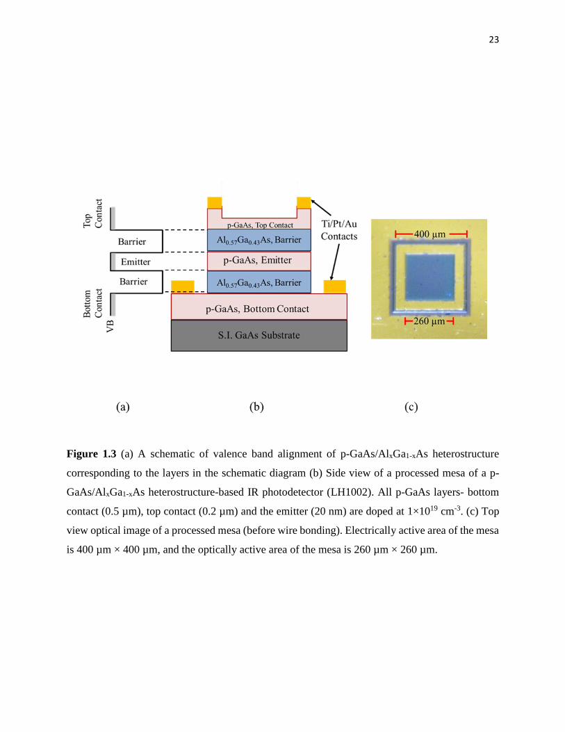
23
Figure 1.3 (a) A schematic of valence band alignment of p-GaAs/AlxGa1-xAs heterostructure
corresponding to the layers in the schematic diagram (b) Side view of a processed mesa of a p-
GaAs/AlxGa1-xAs heterostructure-based IR photodetector (LH1002). All p-GaAs layers- bottom
contact (0.5 µm), top contact (0.2 µm) and the emitter (20 nm) are doped at 1×1019 cm-3. (c) Top
view optical image of a processed mesa (before wire bonding). Electrically active area of the mesa
is 400 µm × 400 µm, and the optically active area of the mesa is 260 µm × 260 µm.
24
temperature controller. A positive voltage connected to the top contact with the bottom contact
grounded contact grounded is referred to as a positive bias. Similarly, a positive voltage connected
to the bottom contact with the top contact grounded is referred to as a negative bias. A Fourier
transform infrared (FTIR) spectrometer (Perkin-Elmer system 2000) was used to measure spectral
photoresponse, and a commercial Si composite bolometer with known sensitivity was used to
measure the background intensity of a blackbody source to calibrate the photoresponse. The
spectral photoresponse measurement set-up is also shown schematically in Appendix C. In
addition, the spectral photoresponse calibration process is also explained in the Appendix C.
1.6.2 Results and Discussion
The experimentally measured dark current of the LH1002 device is shown in Figure 1.4, from 80
K to 200 K, in the applied bias range from -3.0 V to 3.0 V. The theoretical model fitting of the
dark current will be presented in Chapter 3. By design, the device has two identical Al0.57Ga0.43As
barriers (60 nm) with a flat/constant barrier shape. This makes the device a symmetrical one from
the operational point of view in the positive and negative applies biases. The measured current-
voltage characteristics also confirm the symmetrical operation of the device.
The dark current characteristics are important to determine an optimum operating
condition. Whilst the lowest possible dark current is desired for the operation of an IR
photodetector, a certain amount of bias voltage must be applied to operate photo-conductive
photodetectors. With suitable barrier engineering, an optimized operation is possible without an
applied bias in a p-GaAs/ AlxGa1-xAs heterostructure-based IR photodetector (to be presented in
Chapter 4). However, study of dark current characteristics offers important insights into the device
parameters such as activation energy (Δ). Dark current in the semiconductor devices such as
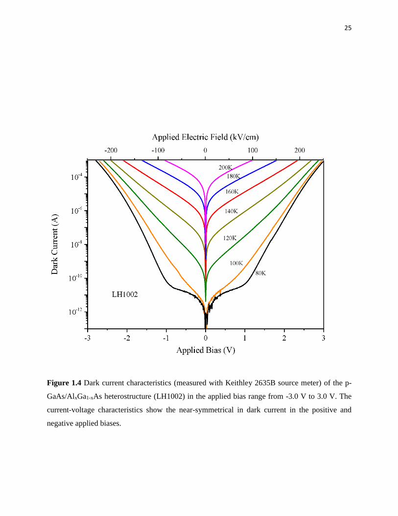
25
Figure 1.4 Dark current characteristics (measured with Keithley 2635B source meter) of the p-
GaAs/AlxGa1-xAs heterostructure (LH1002) in the applied bias range from -3.0 V to 3.0 V. The
current-voltage characteristics show the near-symmetrical in dark current in the positive and
negative applied biases.
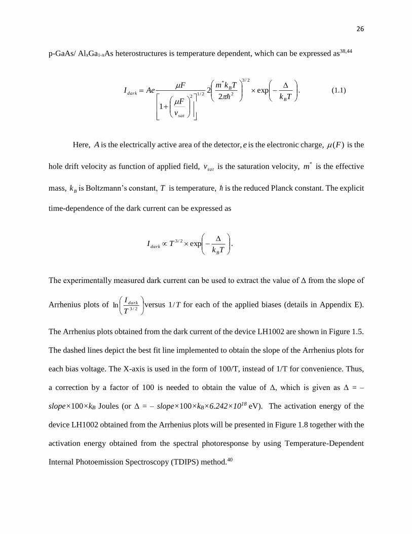
26
p-GaAs/ AlxGa1-xAs heterostructures is temperature dependent, which can be expressed as38,44
−
+
=Tk
Tkm
v
F
FAeI
B
B
sat
dark exp2
2
1
2/3
2
*
2/12
. (1.1)
Here, A is the electrically active area of the detector, e is the electronic charge, )(F is the
hole drift velocity as function of applied field, satv is the saturation velocity, *m is the effective
mass, Bk is Boltzmann’s constant, T is temperature, is the reduced Planck constant. The explicit
time-dependence of the dark current can be expressed as
−
TkTI
B
dark exp2/3 .
The experimentally measured dark current can be used to extract the value of Δ from the slope of
Arrhenius plots of
2/3
lnT
I dark versus T/1 for each of the applied biases (details in Appendix E).
The Arrhenius plots obtained from the dark current of the device LH1002 are shown in Figure 1.5.
The dashed lines depict the best fit line implemented to obtain the slope of the Arrhenius plots for
each bias voltage. The X-axis is used in the form of 100/T, instead of 1/T for convenience. Thus,
a correction by a factor of 100 is needed to obtain the value of Δ, which is given as Δ = –
slope×100×kB Joules (or Δ = – slope×100×kB×6.242×10¹⁸ eV). The activation energy of the
device LH1002 obtained from the Arrhenius plots will be presented in Figure 1.8 together with the
activation energy obtained from the spectral photoresponse by using Temperature-Dependent
Internal Photoemission Spectroscopy (TDIPS) method.40
27
Figure 1.5 The Arrhenius plots of for the device LH1002 obtained from the temperature dependent
dark current, in the temperature range of 100 – 200 K. The dashed lines represent the linear fit to
the each of the plots implemented to obtain the slope of the plots.
28
The spectral photoresponse of the device LH1002 is shown in Figure 1.6 for positive biases and in
Figure 1.7 for negative biases. The photoresponse spectra in the positive and negative biases are
closely comparable at the biases of the same magnitude. The photoresponse due to L-H/H-H to S-
O transitions is limited to ~3.5 µm due to the S-O band energy of 0.34 eV. The strong peak near
the 2.7 µm may be attributed to the direct transitions from the H-H/L-H bands to the S-O band,
whilst indirect transitions contribute for the broad photoresponse spectrum. Beyond ~3.5 µm, the
photoresponse is due to the L-H/H-H intra-valence band absorption, which does not have a clear
minimum energy threshold.45 However, the activation energy imposes the minimum energy limit
on the internal photoemission and escape over the barrier, and hence the wavelength threshold of
the spectral photoresponse. Unlike the natural band-gap between the conduction and valence
bands, interfacial energy gap at the heterojunction is determined by the material type and
composition of the layers forming the heterojunction, therefore, the activation energy can be tuned
by changing the composition, for instance, Al mole fraction x in this study.
A small photoresponse was observed at 0 V, even though this result may not be expected
in the perfectly symmetrical heterostructure. Assuming an isotropic momentum distribution31 of
the photoexcited carriers, the probabilities of emission from emitter to either of the barriers are
equal in the absence of an external applied bias. Thus, a net photocurrent cannot be detected
between the top and the bottom contacts. However, the photoresponse observed at 0 V indicates a
small but finite asymmetry in the heterostructure. Some of the possible reasons for this miniature
asymmetry may be the small but unintentional gradient of the barrier, originating from the epitaxial
growth. With the application of small negative biases, (for example, -0.01 V and -0.015 V as shown
in the inset of Figure 1.7), the effect of this slight asymmetry is observed to get canceled resulting
in a reduced photoresponse signal compared to that at 0 V. Based on the nearly vanishing
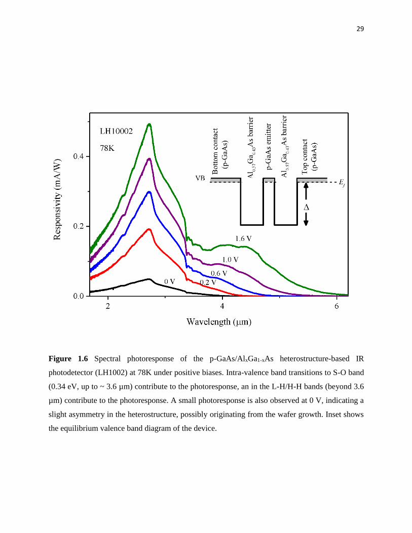
29
Figure 1.6 Spectral photoresponse of the p-GaAs/AlxGa1-xAs heterostructure-based IR
photodetector (LH1002) at 78K under positive biases. Intra-valence band transitions to S-O band
(0.34 eV, up to ~ 3.6 µm) contribute to the photoresponse, an in the L-H/H-H bands (beyond 3.6
µm) contribute to the photoresponse. A small photoresponse is also observed at 0 V, indicating a
slight asymmetry in the heterostructure, possibly originating from the wafer growth. Inset shows
the equilibrium valence band diagram of the device.
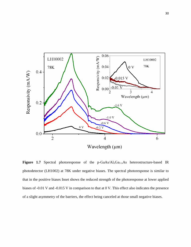
30
Figure 1.7 Spectral photoresponse of the p-GaAs/AlxGa1-xAs heterostructure-based IR
photodetector (LH1002) at 78K under negative biases. The spectral photoresponse is similar to
that in the positive biases Inset shows the reduced strength of the photoresponse at lower applied
biases of -0.01 V and -0.015 V in comparison to that at 0 V. This effect also indicates the presence
of a slight asymmetry of the barriers, the effect being canceled at those small negative biases.
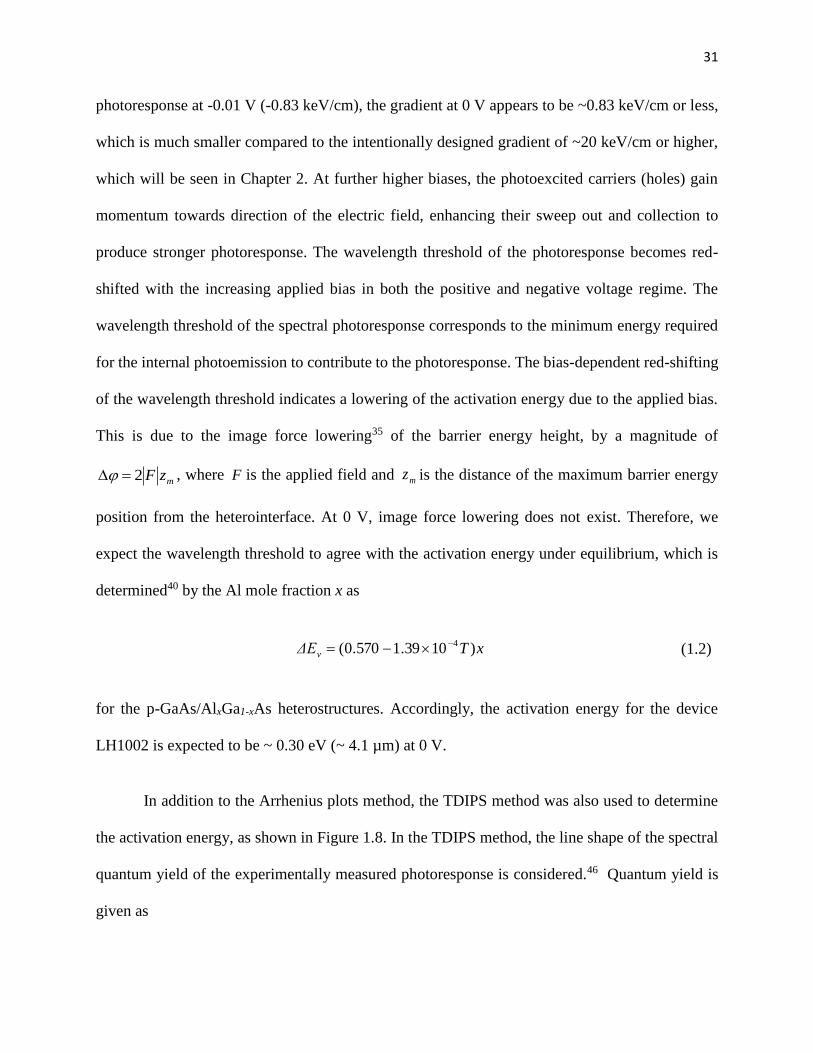
31
photoresponse at -0.01 V (-0.83 keV/cm), the gradient at 0 V appears to be ~0.83 keV/cm or less,
which is much smaller compared to the intentionally designed gradient of ~20 keV/cm or higher,
which will be seen in Chapter 2. At further higher biases, the photoexcited carriers (holes) gain
momentum towards direction of the electric field, enhancing their sweep out and collection to
produce stronger photoresponse. The wavelength threshold of the photoresponse becomes red-
shifted with the increasing applied bias in both the positive and negative voltage regime. The
wavelength threshold of the spectral photoresponse corresponds to the minimum energy required
for the internal photoemission to contribute to the photoresponse. The bias-dependent red-shifting
of the wavelength threshold indicates a lowering of the activation energy due to the applied bias.
This is due to the image force lowering35 of the barrier energy height, by a magnitude of
mzF2= , where F is the applied field and mz is the distance of the maximum barrier energy
position from the heterointerface. At 0 V, image force lowering does not exist. Therefore, we
expect the wavelength threshold to agree with the activation energy under equilibrium, which is
determined40 by the Al mole fraction x as
xTΔEv )1039.1570.0(4−
−= (1.2)
for the p-GaAs/AlxGa1-xAs heterostructures. Accordingly, the activation energy for the device
LH1002 is expected to be ~ 0.30 eV (~ 4.1 µm) at 0 V.
In addition to the Arrhenius plots method, the TDIPS method was also used to determine
the activation energy, as shown in Figure 1.8. In the TDIPS method, the line shape of the spectral
quantum yield of the experimentally measured photoresponse is considered.46 Quantum yield is
given as
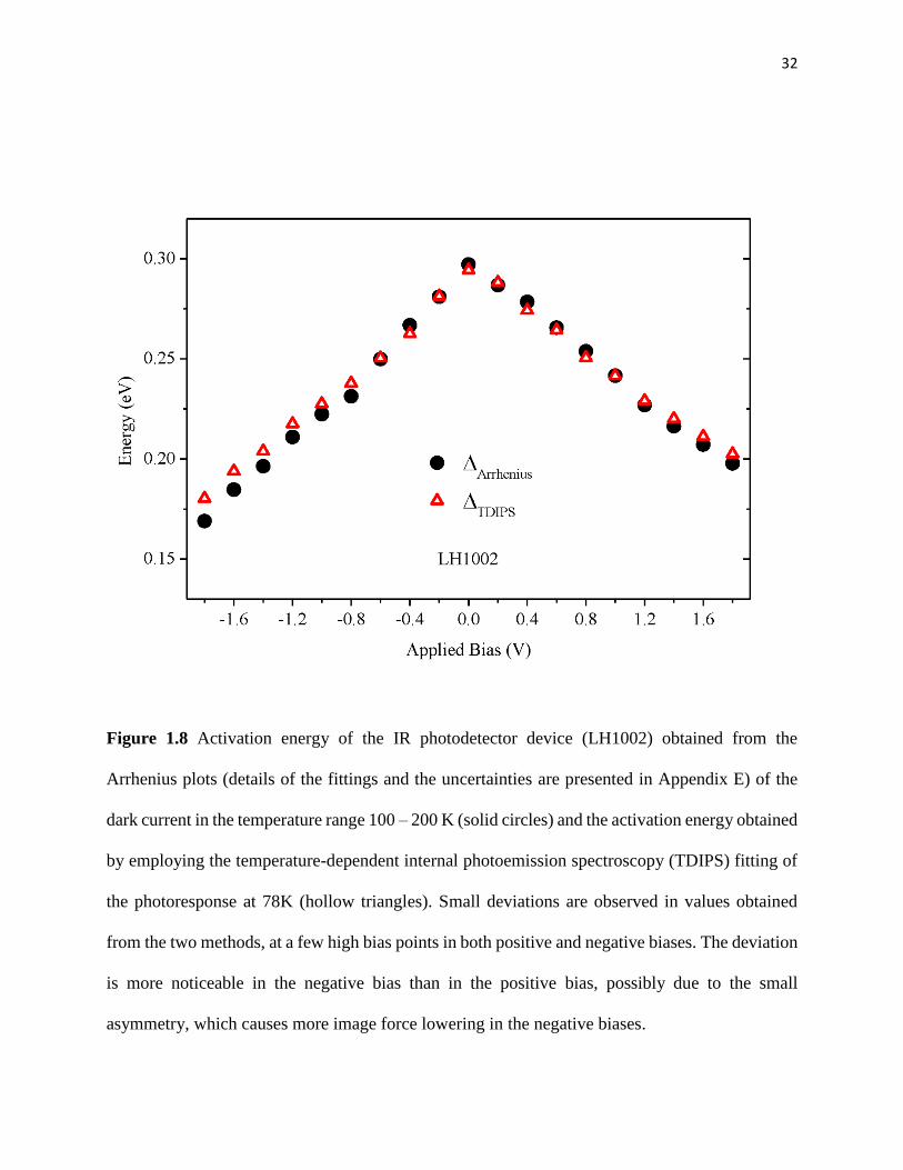
32
Figure 1.8 Activation energy of the IR photodetector device (LH1002) obtained from the
Arrhenius plots (details of the fittings and the uncertainties are presented in Appendix E) of the
dark current in the temperature range 100 – 200 K (solid circles) and the activation energy obtained
by employing the temperature-dependent internal photoemission spectroscopy (TDIPS) fitting of
the photoresponse at 78K (hollow triangles). Small deviations are observed in values obtained
from the two methods, at a few high bias points in both positive and negative biases. The deviation
is more noticeable in the negative bias than in the positive bias, possibly due to the small
asymmetry, which causes more image force lowering in the negative biases.

33
dPEhhfCYhY f ),(),(),()( 00 −+=
, (1.3)
where ),( fEh − is an energy distribution function and ),( P is a probability function and is
calculated by an escape cone model of internal photoemission,30,47,48 0C is a constant, is the
energy of the photoexcited carrier, and is the activation energy to be extracted as a fitting
parameter. The function )1(1),()( kTh
ehf −
+= describes the distribution of the carriers. The
term 0Y accounts for the background signal, for example, the thermionic emersion. It can be
determined by giving the value of experimental quantum yield in the energy range less than the
value of Δ. ),( P is proportional to )( − for , and 0 for . The energy distribution
function ),( 0 of the photo-excited carriers is the key factor to influence on the quantum yield,
and takes form ),( 0 ~ 2/1
0 )( − under a parabolic-band approximation46 near k = 0.
A small region of the spectral quantum yield near the onset of )( hY is selected for the
TDIPS fitting and the value of Δ is obtained as the fitting parameter. In the examples shown in
the Figure 1.9, the experimental spectrum of quantum yield is taken in the energy range of 0.15
eV to 0.39 eV. As can be seen in the Figure, the quantum yield near 0.15 eV appears to be flat at
the background noise level. Therefore, the constant 0Y is provided with the experimental value of
quantum yield near 0.15 eV. The values of 0Y used in the fittings were ~10-6 for 0 V and 10-5 for
both 1 V and -1 V. Similarly, the values of 0Y were used from the experimental quantum yield in
the background noise level for the fitting of the spectral quantum yield at different biases.
Similarly, the energy has a lower limit of Δ, which is a fitting parameter to be determined and
can be different for spectral at different biases. The upper limit of is chosen to be 0.35 eV for
34
0 V spectrum, and 0.28 eV for 1 V and -1 V spectra. Here, primary focus is to obtain a fitting for
near threshold region, therefore the line shape of the quantum yield in this region is considered,
and the line shape of spectra at further higher energies is not important. Thus, the upper limit of
is chosen from energy axis corresponding to a near-parabolic line shape near the threshold of
quantum yield. The constant Co is an arbitrary number that scales the intensity of the fitted curve.
Therefore, the value of Co chosen such that the intensity of the fitted curve matches the
experimental curve. The TDIPS fitting applied to the experimental quantum yield is shown in the
Figure 1.9 for the device LH1002 at 0 V, 1.0 V and -1.0 V on the top, middle, and bottom panels,
respectively. The dashed lines and the solid lines represent the experimental and the fittings curves
respectively.
The activation energy obtained from both the Arrhenius plots and the TDIPS method agree
closely overall as seen in the Figure 1.8. At 0 V, the values of the Δ appear to be in sufficiently
close to the value expected from the design of the heterostructure. Even though a small deviation
of the activation energy obtained from the Arrhenius plots at a few bias points towards both the
negative and positive high bias ends is observed, the Arrhenius plots in general are useful to obtain
activation energy of a heterostructure. The deviation is more noticeable in the negative bias than
in the positive bias, possibly due to the small asymmetry, which causes stronger image force
lowering in the negative biases. However, it should be noted that the TDIPS method takes into
account the actual physical processes occurring in presence of IR radiation onto the photodetector
to produce quantum yield spectra, and this is a more precise method for determining the activation
energy required for internal photoemission.40 Therefore, applications of these two methods may
find their importance under different conditions. For example, activation energy for the internal

35
Figure 1.9 TDIPS fitting of quantum yield for the device LH1002 at 78K to determine the
activation energy (Δ). The top, middle and bottom panel show the fittings curves (solid lines) to
experimental quantum yield (dashed lines) at 0 V, 1.0 V, and -1.0 V, respectively.
36
photoemission determined from the TDIPS may not correspond to the actual interfacial
workfunction under dark conditions at the heterojunction if an extended wavelength photoresponse
mechanism (to be presented in Chapter 2) is observed. In this condition, the Arrhenius plots are
still useful to determine the values of Δ. Nevertheless, the TDIPS offers a standardized procedure
to determine the wavelength threshold as long as experimental quantum yield is available from the
spectral photoresponse, including the extended-wavelength mechanism. The techniques used to
study the p-GaAs/AlxGa1-xAs heterostructure-based IR photodetector here can be applied further
to various III-V semiconductor-based IR photodetectors.
1.7 Summary
Recent research and development on p-type p-GaAs/AlxGa1-xAs heterostructures-based IR
photodetector are summarized. In addition, a study of a single-period, p-GaAs/AlxGa1-xAs
heterostructure-based IR photodetector with constant barriers and no barrier energy offset,
showing a spectral photoresponse in SWIR and MIR spectral regime, due to the S-O band and H-
H/L-H band IVB transitions, has been presented in this Chapter. The simplistic design of this
device will be used as a reference IR photodetector in Chapters 2 and 3, to study the extended-
wavelength IR photodetectors.
37
2 EXTENDED-WAVELENGTH INFRARED PHOTODETECTORS
2.1 Introduction
Conventionally, the fundamental rule that determines the wavelength threshold of the
spectral photoresponse in an IR photodetector is given by the equation35
=hc
t , (2.1)
where t is the wavelength threshold of the photoresponse, and Δ is the minimum energy for the
photo-excitation, also known as the activation energy. However, Δ is no longer a critical parameter
to determine the wavelength threshold of the spectral photoresponse in a novel class of
photodetectors referred to as extended-wavelength IR photodetectors.37,49 In conventional IR
photodetectors, Δ determines not only the wavelength threshold of the spectral photoresponse, but
also the dark current levels.
In this chapter, I will present the study on the photoresponse characteristics of the extended-
wavelength IR photodetectors. In this class of IR photodetectors, the AlxGa1-xAs barriers are
designed to have different barrier heights, thereby setting up an energy offset (𝛿𝐸) between the
two barriers. It has been experimentally found37 that the energy offset is a necessary condition for
the extended wavelength photoresponse. In terms of physical mechanism, the hot-carrier effect36
is deemed to play an important role for the photoresponse in the spectral region beyond the limit
set by Δ as seen in equation (2.1).
Photoexcited carriers are considered as hot-carriers since their energies are larger than
those of thermal excitations at ambient temperatures.50 The discovery of the photoelectric effect

38
by Heinrich Hertz in1887 not only played a critical role in the development of the quantum
mechanics, but also in the study of the photodetectors and solar energy harvesting. The research
interests in this area are still growing. Optoelectronic devices based on hot-carrier driven effects
have received broad attention owing to their breadth of potential applications in areas ranging from
photodetectors to solar energy harvesting.50-52 For example, a hot-carrier based IR photodetector
with wavelength tunability, but independent of the semiconductor bandgap, was explored as one
candidate for IR photodetectors53. Recently, a photo-detection extended up to FIR spectral regime
(~ 55 µm) was demonstrated36 with a photodetector of conventional Δ value corresponding to ~
3.1 µm. In this case, p-GaAs/ AlxGa1-xAs heterostructures with a 𝛿𝐸~0.10 eV were used, where
the p-GaAs layer, sandwiched by AlxGa1-xAs barrier layers, works as an absorber and emitter. The
underlying mechanism leading to this FIR photoresponse is deemed to be the hot-carrier
phenomena in the p-GaAs/AlxGa1-xAs heterostructure device that is barrier-engineered to have a
non-zero 𝛿𝐸.
This study is focused on the further study of the “extended-wavelength IR photodetectors”
in order to obtain a deeper understanding of the extended-wavelength mechanism. The results from
these studies have been published37,38 or is in press.54 Photo-excited carriers have an energy larger
than those in thermal equilibrium,50 and undergo relaxation processes dominated by optical phonon
emission.55 However, a phonon-bottleneck,51,56,57 slows down the hot-carrier relaxation process.
Therefore, the photo-excited carriers will have a transient energy distribution at higher energies
compared to that in the thermal equilibrium, leading to a transient elevation of the Fermi level,
often referred to as the quasi-equilibrium Fermi level. The energy difference between the quasi-
equilibrium Fermi level in the emitter and the height of the emitter-collector barrier thus becomes
smaller, reducing the activation energy for holes to pass to the collector. As a result, a
39
photoresponse can be observed in the extended-wavelength regime, that is, beyond the limit set by
the Δ. The experimental demonstration of the fact that, the Δ related to the band gap of a material
or an interfacial energy gap of a heterostructure can no longer limit the wavelength threshold of
the photoresponse, has offered a novel avenue towards the development of IR photodetectors. A
better understanding of the mechanism of the extended-wavelength IR photoresponse, and the
effect of the device parameters such as the energy offset and the shape of the potential barriers on
the performance of the IR photodetector is crucial towards the advancement of this field.
2.2 Device Parameters for Barrier Offset and Gradient Variation
The p-GaAs/AlxGa1-xAs heterostructure devices (LH1002, SP1001, SP1007, 15SP3,
GSU17I, GSU17II, GSU17III) were grown on semi-insulating GaAs substrate by molecular beam
epitaxy.43 The details of the device LH1002 have been presented in Chapter 1. For all other
heterostructure devices, a schematic of the sideview of the heterostructure layers is depicted in
Figure 2.1. Each heterostructure device consists of an AlxGa1-xAs barrier at the bottom, followed
by a p-GaAs emitter, and then another AlxGa1-xAs barrier at the top. The bottom AlxGa1-xAs barrier
is graded by increasing Al mole fraction from a lower value x1 at the bottom of this layer to higher
value x2 at the top, except for SP1001 with x1 = x2 to form a constant barrier. These emitter/barrier
layers are sandwiched between the bottom and top contact layers of p-type doped GaAs, with
thicknesses of 0.5 µm and 0.2 µm, respectively. The emitter, and the top and bottom contact
layers, are degenerately p-type doped at 1×1019 cm-3, whilst the AlxGa1-xAs barriers are undoped.
The thickness of the p-GaAs emitter in all devices is sufficiently large to have a bulk-like
distribution of energy states.58 The emitter thicknesses of 80 nm were chosen to be comparable to
the carrier-carrier scattering length34 (~80 nm), which also changes with the doping level, to
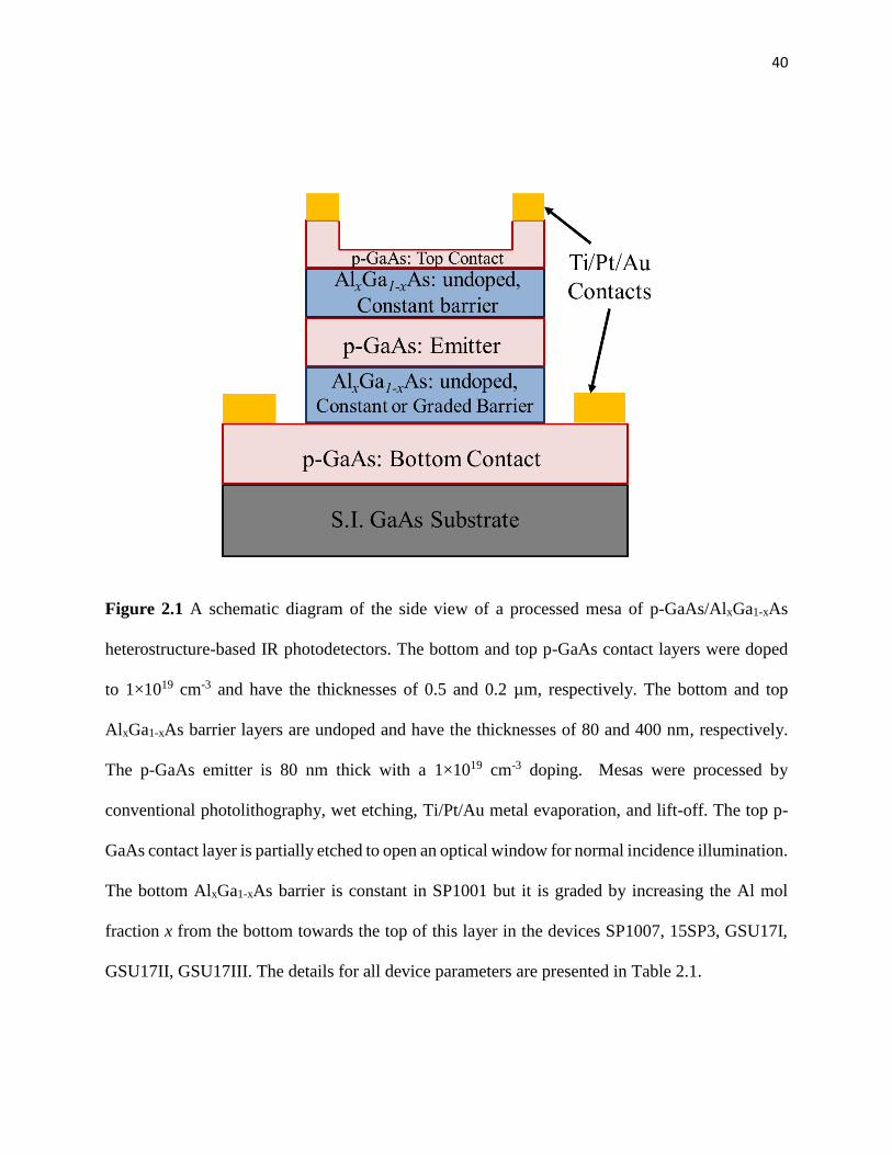
40
Figure 2.1 A schematic diagram of the side view of a processed mesa of p-GaAs/AlxGa1-xAs
heterostructure-based IR photodetectors. The bottom and top p-GaAs contact layers were doped
to 1×1019 cm-3 and have the thicknesses of 0.5 and 0.2 µm, respectively. The bottom and top
AlxGa1-xAs barrier layers are undoped and have the thicknesses of 80 and 400 nm, respectively.
The p-GaAs emitter is 80 nm thick with a 1×1019 cm-3 doping. Mesas were processed by
conventional photolithography, wet etching, Ti/Pt/Au metal evaporation, and lift-off. The top p-
GaAs contact layer is partially etched to open an optical window for normal incidence illumination.
The bottom AlxGa1-xAs barrier is constant in SP1001 but it is graded by increasing the Al mol
fraction x from the bottom towards the top of this layer in the devices SP1007, 15SP3, GSU17I,
GSU17II, GSU17III. The details for all device parameters are presented in Table 2.1.

41
minimize carrier loss due to the scattering. The IR absorption properties of p-GaAs have been
studied in a wide range of doping levels39 ( ~1017 to 1020 cm-3). The doping level also causes a shift
in the Fermi level, thus a 1×1019 cm-3 level was chosen to get the Fermi level near valence band
edge based on the recommendation from the theoretical study34. A schematic of the valence band
of the heterostructures is depicted in Figure 2.2 to illustrate the differences in the devices in terms
of barrier engineering. The details of each device parameters are summarized in Table 2.1. The
device LH1002 serves as a reference IR photodetector due to the absence of an energy offset (𝛿𝐸 =
0) and constant Al0.57Ga0.43As barriers. The device SP1001 consists of an energy offset
(𝛿𝐸 ~ 0.10 𝑒𝑉) but both the bottom Al0.57Ga0.43As barrier and the top Al0.75Ga0.25As have constant
potential profile. Thus, a comparison between the experimental results from LH1002 and SP1001
will highlight the effect of a non-zero barrier offset. The device SP1007 is similar to SP1001 in all
aspects, except for the graded bottom barrier, which is achieved by increasing the Al mole fraction
from x1 = 0.45 at the bottom of this layer to x2 = 0.75 at the top. This difference between SP1001
and SP1007 allows us to compare the extended-wavelength photoresponse with the shape of
AlxGa1-xAs barrier as will be seen in section 2.4.2. The study of the intensity and wavelength
threshold of extended-wavelength photoresponse on the set of devices with 𝛿𝐸 variation will be
presented in the section 2.4.3, and the study on the set of devices with the gradient variation in the
section 2.4.5.
The devices SP1007, 15SP3, and GSU17I constitute a set with an increasing energy offset
(𝛿𝐸) between the two AlxGa1-xAs barriers. The offset in the three devices SP1007, 15SP3, and
GSU17I have the offset values of 𝛿𝐸 ~ 0.10, 0.19, and 0.23 eV, respectively, corresponding to the
Al mole fraction of x3 (= x4) = 0.57, 39, and 30, respectively on the AlxGa1-xAs barrier. All other
parameters have the same values in these three devices.
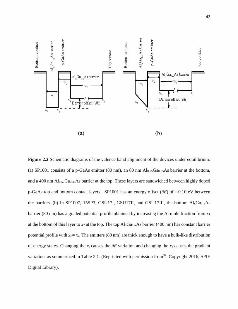
42
Figure 2.2 Schematic diagrams of the valence band alignment of the devices under equilibrium:
(a) SP1001 consists of a p-GaAs emitter (80 nm), an 80 nm Al0.75Ga0.25As barrier at the bottom,
and a 400 nm Al0.57Ga0.43As barrier at the top. These layers are sandwiched between highly doped
p-GaAs top and bottom contact layers. SP1001 has an energy offset (δE) of ∼0.10 eV between
the barriers. (b) In SP1007, 15SP3, GSU17I, GSU17II, and GSU17III, the bottom AlxGa1-xAs
barrier (80 nm) has a graded potential profile obtained by increasing the Al mole fraction from x1
at the bottom of this layer to x2 at the top. The top AlxGa1-xAs barrier (400 nm) has constant barrier
potential profile with x3 = x4. The emitters (80 nm) are thick enough to have a bulk-like distribution
of energy states. Changing the x3 causes the δE variation and changing the x1 causes the gradient
variation, as summarized in Table 2.1. (Reprinted with permission from37. Copyright 2016, SPIE
Digital Library).
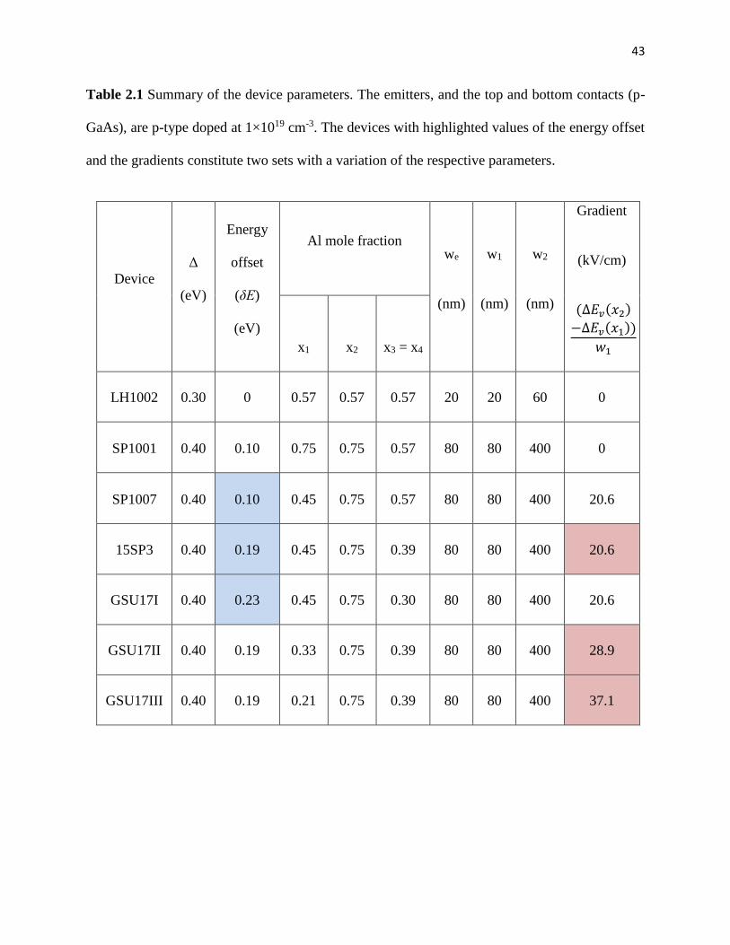
43
Table 2.1 Summary of the device parameters. The emitters, and the top and bottom contacts (p-
GaAs), are p-type doped at 1×1019 cm-3. The devices with highlighted values of the energy offset
and the gradients constitute two sets with a variation of the respective parameters.
Device
Δ
(eV)
Energy
offset
(δE)
(eV)
Al mole fraction we
(nm)
w1
(nm)
w2
(nm)
Gradient
(kV/cm)
(∆𝐸𝑣(𝑥2)
−∆𝐸𝑣(𝑥1))
𝑤1
x1 x2 x3 = x4
LH1002 0.30 0 0.57 0.57 0.57 20 20 60 0
SP1001 0.40 0.10 0.75 0.75 0.57 80 80 400 0
SP1007 0.40 0.10 0.45 0.75 0.57 80 80 400 20.6
15SP3 0.40 0.19 0.45 0.75 0.39 80 80 400 20.6
GSU17I 0.40 0.23 0.45 0.75 0.30 80 80 400 20.6
GSU17II 0.40 0.19 0.33 0.75 0.39 80 80 400 28.9
GSU17III 0.40 0.19 0.21 0.75 0.39 80 80 400 37.1

44
Similarly, 15SP3, GSU17I, and GSU17II constitute another set with varying values of the
gradient ~ 20.6, 28.9, and 37.1 kV/cm, given by (ΔEv(x2) – ΔEv(x1))/w1 for x1 = 0.45, 0.33, and
0.21, respectively. The gradients are the only differences in these three devices. It should be noted
that the device 15SP3 is common in both sets with an 𝛿𝐸 ~ 0.19 eV and gradient 20.6 kV/cm.
The MBE growth and the mesa processing of the devices is similar to the processes
explained in Chapter 1.6.1. The packaging (mounting and wire-bonding on a chip carrier) is
explained in Appendix A.
2.3 Experimental Measurements
The experimental characterizations of the p-GaAs/AlxGa1-xAs heterostructure devices
listed on Table 2.1 (LH1002, SP1001, SP1007, 15SP3, GSU17I, GSU17II, GSU17III) were carried
out by following the procedure described in Chapter 1.5. Perkin Elmer system 2000 FTIR
spectrometer with Spectrum 5.0 software was used for photoresponse measurements. A bolometer
with known sensitivity was to measure the intensity of the spectrum of IR radiation from the built-
in IR source in FTIR spectrometer. Vacuum dewar for IR measurements (HD-3 or HD-5, IR Lab
Inc.) was used for mounting the detector under test and bolometer. Incoming IR radiation from the
IR source in FTIR spectrometer was focused onto the detector under test and bolometer by a
Winston cone. The photoresponse spectrum of the bolometer measured under similar optical set
up with the detectors under test was used to calibrate the photoresponse of the detectors by
following the methods outlined in Chapter 1.5. Current-voltage characteristics under dark
conditions were measured by using Keithley 2635B (or Keithley 2400) by mounting the detector
onto the sample holder of cold finger of a cryostat. The cold finger was covered with shrouds and
pumped to ~10-6 Torr and cooled to cryogenic temperatures by an APD HC2 closed-cycle
45
refrigerator. A DC bias voltage is applied to the detector by the source meter where a positive bias
refers to the voltage connected to the top contact electrode of the device under test with the bottom
contact grounded and a negative bias refers to the voltage connected to the bottom contact with
the top contact being grounded. Dark current-voltage characteristics were measured from 10 K to
room temperature with the temperature steps being controlled by a Lakeshore 330 temperature
controller.
2.4 Results and Discussion
2.4.1 Dark Current and Photoresponse Characteristics of Device 15SP3
A detailed study of the experimental results of the will be presented to study the extended-
wavelength photoresponse mechanism by comparing the experimental results of the devices
LH1002, SP1001, SP1007, 15SP3, GSU17I, GSU17II, GSU17III in the next section and onwards.
In this section, the device 15SP3 is selected to present its detail device characterizations and
results.
Dark current-voltage characteristics of the device 15SP3 is presented in Figure 2.3. An
asymmetrical bias dependence of dark current is observed. This asymmetry in can be related to the
fact that the p-GaAs/AlxGa1-xAs heterostructure is asymmetrical in nature owing to the graded
barrier and an energy offset between the barriers as depicted in its valence band alignment in Figure
2.2 (b). Further detail study of the dark current characteristics with a theoretical model will be
presented in Chapter 3. Here, Arrhenius plots obtained from the dark current of the device 15SP3
are presented in Figure 2.4 (a). The method of obtaining the plots are explained in Chapter 1.6.2.
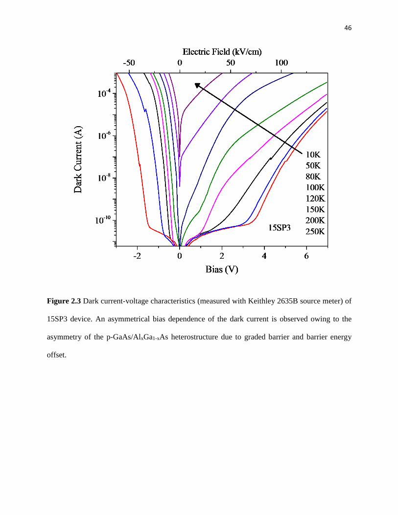
46
Figure 2.3 Dark current-voltage characteristics (measured with Keithley 2635B source meter) of
15SP3 device. An asymmetrical bias dependence of the dark current is observed owing to the
asymmetry of the p-GaAs/AlxGa1-xAs heterostructure due to graded barrier and barrier energy
offset.

47
Figure 2.4 (a) Arrhenius plots for device 15SP3 obtained from the dark current measurements.
The dashed line represents the linear fit applied to the Arrhenius plot in order to obtain the slope
of the plot. (b) The activation energy of the device 15SP3 obtained from the slope of Arrhenius
plots. The activation energy decreases with the increasing bias voltage due to image force lowering
of the barrier height. The asymmetrical bias dependence is the result of the asymmetry of the
p-GaAs/AlxGa1-xAs heterostructure due to the graded barrier and energy offset of the barrier.
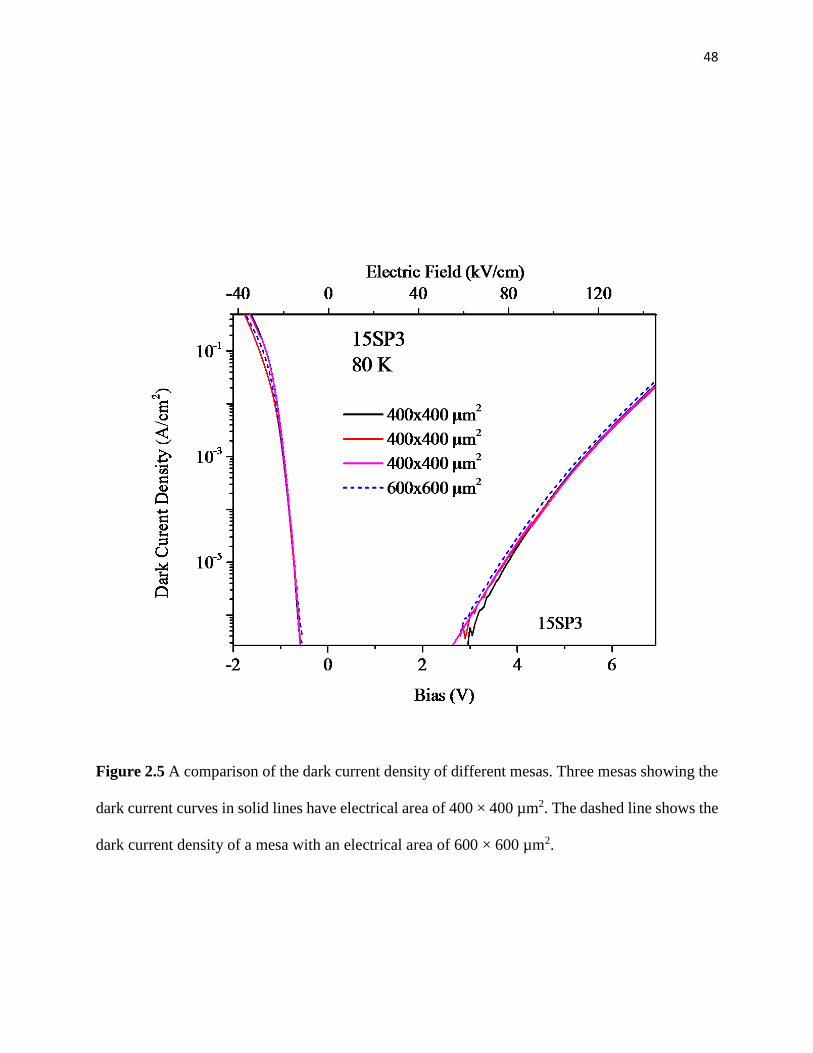
48
Figure 2.5 A comparison of the dark current density of different mesas. Three mesas showing the
dark current curves in solid lines have electrical area of 400 × 400 µm2. The dashed line shows the
dark current density of a mesa with an electrical area of 600 × 600 µm2.
49
From the plots of
2/3
lnT
I dark versus T/100 as shown in Figure 2.4 (a), a linear fit of the plot was
used to obtain the slope of the plot shown by the dashed line. Then slope was used to obtain the
activation energy (Δ = – slope×100×kB×6.242×10¹⁸ eV) of the device 15SP3 as shown in Figure
2.4 (b). The activation energy decreases with the increasing bias voltage due to image force
lowering of the barrier height. The asymmetrical bias dependence is the result of the asymmetry
of the p-GaAs/AlxGa1-xAs heterostructure due to the graded barrier and energy offset of the barrier.
Furthermore, dark current density (current per unit area) of different mesas were compared
in order to assess the uniformity between different mesas. A comparison of the dark current density
of different mesas is shown in Figure 2.5. Solid lines represent the dark current density of the three
mesas with electrical area of 400 × 400 µm2. The dashed line represents the dark current density
of a mesa with an electrical area of 600 × 600 µm2. These results show a considerable uniformity
of the mesas.
The device operation of spectral photoresponse measurements of a of p-GaAs/AlxGa1-xAs
heterostructure IR detector with graded barrier and barrier energy offset under an applied bias
voltage is depicted in Figure 2.6 (a). The applied bias causes the barrier bending, whereas the
emitter energy band is not affected significantly owing to its high doping level that leads to
insignificant voltage drop across it. Arrows show possible optical transitions to S-O band due to
the absorption of IR photons that leads to the emission of the photo-excited carriers to the barrier.
The partially etched top contact p-GaAs layer also contributes to the photoresponse. The spectral
photoresponse of the device 15SP3 measured at 5.3 K with -1 V bias voltage is shown in Figure
2.6 (b). Ten of such photoresponse spectra are plotted on the top of each other. The background

50
Figure 2.6 (a) A schematic representation of operation of an IR detector with barrier gradient and
offset under a negative bias, which causes a barrier bending. Arrows show the possible transitions
to S-O band. (b) Spectral responsivity and specific detectivity of 15SP3 measured at 5.3 K with -
1 V bias showing extended-wavelength photoresponse to 60.0 ± 0.4 µm. Ten spectra are plotted
on the top of each other. Also, ten spectra of the background noise level measured by blocking the
IR source are also shown, where the dark solid curve is the average of ten noise spectra. Inset
shows the expended view of near threshold spectra to compare with the average noise level.

51
noise level was also measured by blocking the IR radiation and ten of such background noise
spectra are plotted in the Figure 2.6 (b) together with the photoresponse spectra. The dark solid
curve represents the average of ten background noise spectra. Inset in Figure 2.6 (b) shows the
expanded view of near threshold region of photoresponse showing the comparison of the
photoresponse spectra to with the average background noise level. The wavelength at which the
photoresponse signal becomes the same as the background noise level is noted to find out the
wavelength threshold. The wavelength threshold of the spectral photoresponse by this comparison
is found to be 60.0 ± 0.4 µm. In the remaining part of this study, the TDIPS fitting will be used to
determine the wavelength threshold of the photoresponse. The specific detectivity was estimated
by using
diff
Bd
i
R
TkqI
ARD
42
*
+
= , and a peak value of D* was found to be 2.7×10⁹ Jone near 35 µm.
As discussed before, the primary focus of this study is to understand the extended-
wavelength mechanism, a comparative study of the the spectral photoresponse of the different
devices will be carried out based on the parameters of the each heterostructure.
2.4.2 Spectral photoresponse: Non-zero barrier energy offset vs zero barrier energy
offset; and the graded barrier vs the constant barrier
The photoresponse from LH1002 at 5.3K was observed in a spectral regime nearly up to
4.5 µm at -0.2 V, without an indication of extended-wavelength mechanism, as shown in Figure
2.7. This device serves as the reference IR photodetector in terms of barrier energy offset due to
the absence of the offset (i.e., δE = 0 eV) and standard (flat band) barriers. A small deviation from
the zero-bias wavelength threshold (~4.1 µm), is the effect of the image force barrier lowering due
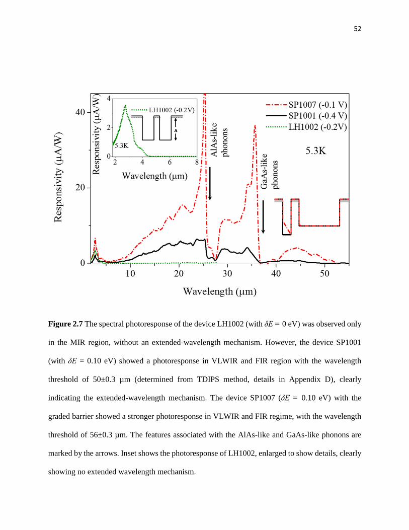
52
Figure 2.7 The spectral photoresponse of the device LH1002 (with δE = 0 eV) was observed only
in the MIR region, without an extended-wavelength mechanism. However, the device SP1001
(with δE = 0.10 eV) showed a photoresponse in VLWIR and FIR region with the wavelength
threshold of 50±0.3 µm (determined from TDIPS method, details in Appendix D), clearly
indicating the extended-wavelength mechanism. The device SP1007 (δE = 0.10 eV) with the
graded barrier showed a stronger photoresponse in VLWIR and FIR regime, with the wavelength
threshold of 56±0.3 µm. The features associated with the AlAs-like and GaAs-like phonons are
marked by the arrows. Inset shows the photoresponse of LH1002, enlarged to show details, clearly
showing no extended wavelength mechanism.
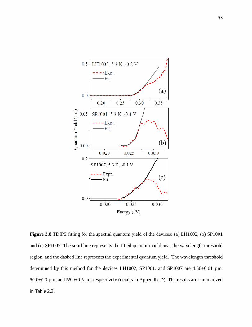
53
Figure 2.8 TDIPS fitting for the spectral quantum yield of the devices: (a) LH1002, (b) SP1001
and (c) SP1007. The solid line represents the fitted quantum yield near the wavelength threshold
region, and the dashed line represents the experimental quantum yield. The wavelength threshold
determined by this method for the devices LH1002, SP1001, and SP1007 are 4.50±0.01 µm,
50.0±0.3 µm, and 56.0±0.5 µm respectively (details in Appendix D). The results are summarized
in Table 2.2.
54
to applied bias (similar to the photoresponse at 78 K, Chapter 1.6.2). In contrast, SP1001 with δE
~ 0.10 eV showed the photoresponse in the VLWIR and FIR regime, up to ~50 µm, at 5.3 K and
-0.4 V, clearly indicating the extended-wavelength mechanism. Without an extended-wavelength
mechanism, the spectral photoresponse would be limited to MIR regime, corresponding to Δ =
0.40 eV (~3.1 µm). The striking difference in the spectral range of the photoresponse in the device
SP001 as opposed to LH1002 due to the presence of the energy offset in SP1001. Next, the
photoresponse of the device SP1007 with the same the same value of the offset (δE ~ 0.10 eV) but
with a graded bottom AlxGa1-xAs barrier showed a stronger photoresponse with the extended-
wavelength mechanism up to ~56 µm, at 5.3 K with a bias of -0.1 V. Overall, the shape of the
photoresponse spectra appear for both SP1001 and SP1007 to be similar, with the differences in
only in the intensity, mainly in the FIR spectral regime. Furthermore, the same features associated
with AlAs-like and GaAs-like phonons are observed, which are marked by the arrows in the Figure
2.7. The TDIPS fitting applied to determine the wavelength threshold of the spectral quantum yield
of the devices LH1002, SP1001, and SP1007 is shown in Figure 2.8.
The results, in general, confirm that the barrier energy offset is a necessary condition for
the extended-wavelength mechanism, whilst a graded barrier (SP1007) is found to be related to a
higher photoresponse as opposed to a constant barrier (SP1001). The negative bias operation drives
the carrier injection from the bottom contact over the bottom barrier to the emitter, and the
collection at the top contact. The graded barrier was suggested to be included in the device to
improve the performance by reducing the carrier trapping,34 and hence may be related to what has
been observed in the photoresponse of SP1007 compared to SP1001. However, the existence of
55
similar nature of extended-wavelength mechanism for both SP1001 and SP1007 can be inferred
based on the similar spectral shape and extended-wavelength thresholds (compared to the
conventional limits ~3.1µm), even though the exact physical processes underlying the mechanism
are yet to be fully understood. The detailed bias-dependence spectral photoresponse of SP1007 has
been published36, showing that the photoresponse up to FIR regime (~55 µm) due to extended-
wavelength mechanism was observed only in a narrow range of applied biases smaller than -0.2
V. For the higher values of the negative applied biases, the spectral photoresponse was observed
only in the MIR regime (< 7 µm).
2.4.3 Spectral photoresponse with barrier energy offset variation
It is desirable to find an operating condition for optimized performance of the IR
photodetector. One of the improvements needed for optimization is to overcome the limitation of
the extended-wavelength mechanism in a narrow region of low applied biases, since the intensity
of the photoresponse is usually weak at low biases. Furthermore, a deeper understanding of the
extended-wavelength mechanism requires further study of the heterostructure devices to determine
the effects of the variation in the device parameters. Since the barrier energy offset is found to be
a critical parameter, further study with a change in the value of this parameter is important.
Therefore, the next study was carried out in the device 15SP3, which is similar to the SP1007 in
all aspects, except with a higher barrier energy offset (δE ~ 0.19 eV) with the Al mole fraction x3
(= x4) = 0.39 in the top AlxGa1-xAs barrier. The spectral photoresponse of the device 15SP3 was
observed up to FIR regime, as shown in Figure 2.9, owing to extended-wavelength mechanism.
Without the extended-wavelength mechanism, the photoresponse of this device would be limited
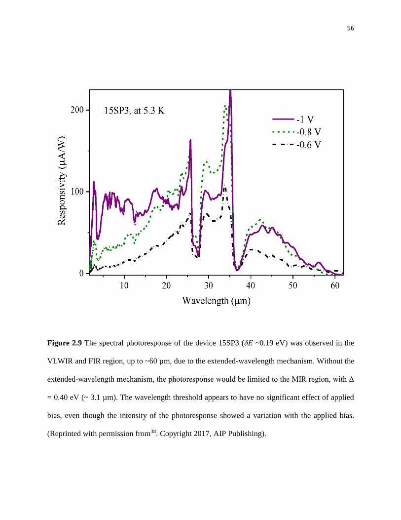
56
Figure 2.9 The spectral photoresponse of the device 15SP3 (δE ~0.19 eV) was observed in the
VLWIR and FIR region, up to ~60 µm, due to the extended-wavelength mechanism. Without the
extended-wavelength mechanism, the photoresponse would be limited to the MIR region, with Δ
= 0.40 eV (~ 3.1 µm). The wavelength threshold appears to have no significant effect of applied
bias, even though the intensity of the photoresponse showed a variation with the applied bias.
(Reprinted with permission from38. Copyright 2017, AIP Publishing).
57
to the MIR regime. In contrast to the device SP1007, the photoresponse due to extended-
wavelength mechanism is not limited to a small range of applied biases. Moreover, the wavelength
threshold of the spectral photoresponse appears to have no significant variation with the applied
biases even though the intensity of the photoresponse showed a variation with the applied biases.
In general, shape of the photoresponse spectra in the device 15SP3 is similar to that in the device
SP1007, indicating that the nature of the extended-wavelength mechanism has not altered.
However, the intensity of the photoresponse is significantly higher in 15SP3 compared to that in
SP1007. The improvements can be attributed to the higher barrier energy offset (δE ~0.19 eV) in
the device 15SP3, since the offset is the only difference in this device compared to SP1007 (δE
~0.10 eV).
The encouraging results from the device 15SP3 motivated us to take this study a step
further by increasing the barrier energy offset. The offset was increased to a further higher value,
δE ~0.23 eV, in the design of the next device GSU17I, with the Al mole fraction x3 (= x4) = 0.30
in the top AlxGa1-xAs barrier. It should be noted that the increased barrier energy offset is achieved
by lowering the top AlxGa1-xAs barrier energy, without any change in the bottom graded AlxGa1-
xAs barrier. Therefore, the other operating conditions such as carrier injection from the bottom
contact over the graded barrier will not be altered. The spectral photoresponse of the device
GSU17I is shown in Figure 2.10. The photoresponse was observed in the VLWIR and FIR spectral
regime, up to ~61 µm due to extended-wavelength mechanism. The intensity of the photoresponse
was found to increase with the applied bias, but a significant effect was not observed in terms of
wavelength threshold. In comparison to the device 15SP3, a higher photoresponse was observed
in GSU17I.
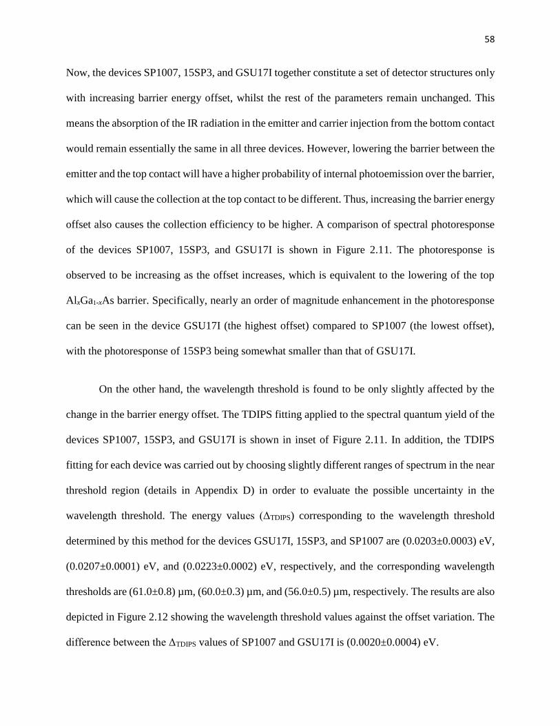
58
Now, the devices SP1007, 15SP3, and GSU17I together constitute a set of detector structures only
with increasing barrier energy offset, whilst the rest of the parameters remain unchanged. This
means the absorption of the IR radiation in the emitter and carrier injection from the bottom contact
would remain essentially the same in all three devices. However, lowering the barrier between the
emitter and the top contact will have a higher probability of internal photoemission over the barrier,
which will cause the collection at the top contact to be different. Thus, increasing the barrier energy
offset also causes the collection efficiency to be higher. A comparison of spectral photoresponse
of the devices SP1007, 15SP3, and GSU17I is shown in Figure 2.11. The photoresponse is
observed to be increasing as the offset increases, which is equivalent to the lowering of the top
AlxGa1-xAs barrier. Specifically, nearly an order of magnitude enhancement in the photoresponse
can be seen in the device GSU17I (the highest offset) compared to SP1007 (the lowest offset),
with the photoresponse of 15SP3 being somewhat smaller than that of GSU17I.
On the other hand, the wavelength threshold is found to be only slightly affected by the
change in the barrier energy offset. The TDIPS fitting applied to the spectral quantum yield of the
devices SP1007, 15SP3, and GSU17I is shown in inset of Figure 2.11. In addition, the TDIPS
fitting for each device was carried out by choosing slightly different ranges of spectrum in the near
threshold region (details in Appendix D) in order to evaluate the possible uncertainty in the
wavelength threshold. The energy values (ΔTDIPS) corresponding to the wavelength threshold
determined by this method for the devices GSU17I, 15SP3, and SP1007 are (0.0203±0.0003) eV,
(0.0207±0.0001) eV, and (0.0223±0.0002) eV, respectively, and the corresponding wavelength
thresholds are (61.0±0.8) µm, (60.0±0.3) µm, and (56.0±0.5) µm, respectively. The results are also
depicted in Figure 2.12 showing the wavelength threshold values against the offset variation. The
difference between the ΔTDIPS values of SP1007 and GSU17I is (0.0020±0.0004) eV.
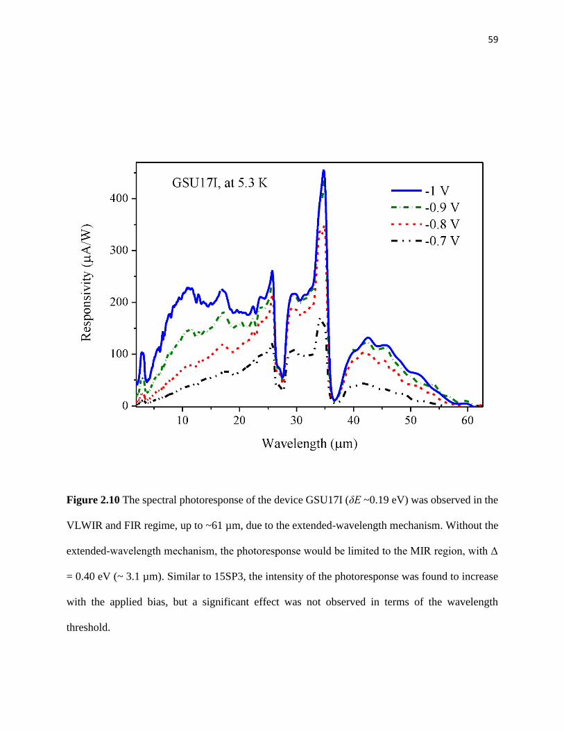
59
Figure 2.10 The spectral photoresponse of the device GSU17I (δE ~0.19 eV) was observed in the
VLWIR and FIR regime, up to ~61 µm, due to the extended-wavelength mechanism. Without the
extended-wavelength mechanism, the photoresponse would be limited to the MIR region, with Δ
= 0.40 eV (~ 3.1 µm). Similar to 15SP3, the intensity of the photoresponse was found to increase
with the applied bias, but a significant effect was not observed in terms of the wavelength
threshold.
60
Figure 2.11 A comparison of the spectral photoresponse of the devices SP1007 (δE ~0.10 eV),
15SP3 (δE ~0.19 eV), and GSU17I (δE ~0.23 eV). The photoresponse is observed to be increasing
as the barrier energy offset increases. The photoresponse of the device SP1007 is scaled-up by a
factor of two for a better visualization. Inset: TDIPS fitting for the spectral quantum yield of the
devices GSU17I, 15SP3, and SP1007. The solid line represents the fitted quantum yield near the
wavelength threshold region, and the dashed line represents the experimental quantum yield. The
energy values (ΔTDIPS) corresponding to the wavelength threshold determined by this method for
the devices GSU17I, 15SP3, and SP1007 are (0.0203±0.0003) eV, (0.0207±0.0001) eV, and
(0.0223±0.0002) eV, respectively, and the corresponding wavelength thresholds are (61.0±0.8)
µm, (60.0±0.3) µm, and (55.6±0.5) µm, respectively (details in Appendix D). The wavelength
threshold is found to be only slightly affected by the changes in the barrier energy offset. The
results are summarized in Table 2.2. (Reprinted with permission from54. Copyright 2018, IEEE).

61
Figure 2.12 A graphical depiction of the wavelength thresholds of the extended-wavelength
photoresponse of the three devices SP1007, 15SP3, and GSU17I (with the increasing barrier
energy offset values). The wavelength thresholds are (61.0±0.8) µm, (60.0±0.3)µm, and (55.6±0.5)
µm, and the corresponding threshold energy values are (0.0203±0.0003) eV, (0.0207±0.0001) eV,
and (0.0223±0.0002) eV, respectively.
62
By comparison, the barrier energy offset from SP1007 to GSU17I changes by a magnitude of
~0.13 eV >> 0.0020 eV, the corresponding change in the value of ΔTDIPS. Therefore, the effect of
the change in the barrier energy offset on the wavelength threshold is found to be insignificant.
These findings have two implications regarding the extended-wavelength mechanism. The
first is that the quasi-equilibrium Fermi level, which causes the extended-wavelength
photoresponse, is practically unchanged from device to device, irrespective of the barrier energy
offset. The second is that the increasing spectral photoresponse with the increasing barrier offset
is due to the lowering of the top AlxGa1-xAs barrier and hence higher probability of internal
photoemission and escape over the barrier.
It was suggested that the formation of the quasi-equilibrium Fermi level is the result of
interaction between hot-carriers, injected from the bottom contact to the emitter, and the cold-
carriers in the emitter.36 To test this idea, incident IR radiation from the FTIR source in the MIR
regime was blocked using long-pass cut-on filters with the cut-on wavelengths of λCO = 2.4, 3.6,
and 4.5 µm. The results showed that the VLWIR and FIR photoresponse became weaker with
increasing cut-on wavelengths and vanished with λCO = 4.5 µm. With the λCO = 4.5 µm filter still
in place, the VLWIR and FIR photoresponse was recovered with the exposure of an external MIR
source. These results led to the deduction that the hot-carrier injection, with the excitation source
with IR radiation of wavelengths shorter that 4.5 µm is needed for a quasi-equilibrium Fermi level
to build up in the emitter to enable the VLWIR and FIR photoresponse.36 However, the origin of
the VLWIR and FIR photoresponse without an applied bias (i.e., 0 V) cannot be understood based
on this explanation, which will be discussed next.
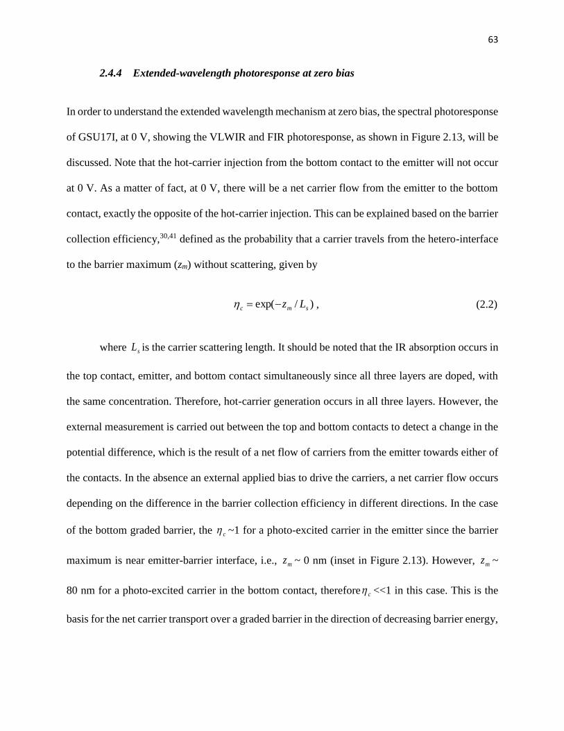
63
2.4.4 Extended-wavelength photoresponse at zero bias
In order to understand the extended wavelength mechanism at zero bias, the spectral photoresponse
of GSU17I, at 0 V, showing the VLWIR and FIR photoresponse, as shown in Figure 2.13, will be
discussed. Note that the hot-carrier injection from the bottom contact to the emitter will not occur
at 0 V. As a matter of fact, at 0 V, there will be a net carrier flow from the emitter to the bottom
contact, exactly the opposite of the hot-carrier injection. This can be explained based on the barrier
collection efficiency,30,41 defined as the probability that a carrier travels from the hetero-interface
to the barrier maximum (zm) without scattering, given by
)/exp( smc Lz−= , (2.2)
where sL is the carrier scattering length. It should be noted that the IR absorption occurs in
the top contact, emitter, and bottom contact simultaneously since all three layers are doped, with
the same concentration. Therefore, hot-carrier generation occurs in all three layers. However, the
external measurement is carried out between the top and bottom contacts to detect a change in the
potential difference, which is the result of a net flow of carriers from the emitter towards either of
the contacts. In the absence an external applied bias to drive the carriers, a net carrier flow occurs
depending on the difference in the barrier collection efficiency in different directions. In the case
of the bottom graded barrier, the c ~1 for a photo-excited carrier in the emitter since the barrier
maximum is near emitter-barrier interface, i.e., mz ~ 0 nm (inset in Figure 2.13). However, mz ~
80 nm for a photo-excited carrier in the bottom contact, therefore c <<1 in this case. This is the
basis for the net carrier transport over a graded barrier in the direction of decreasing barrier energy,
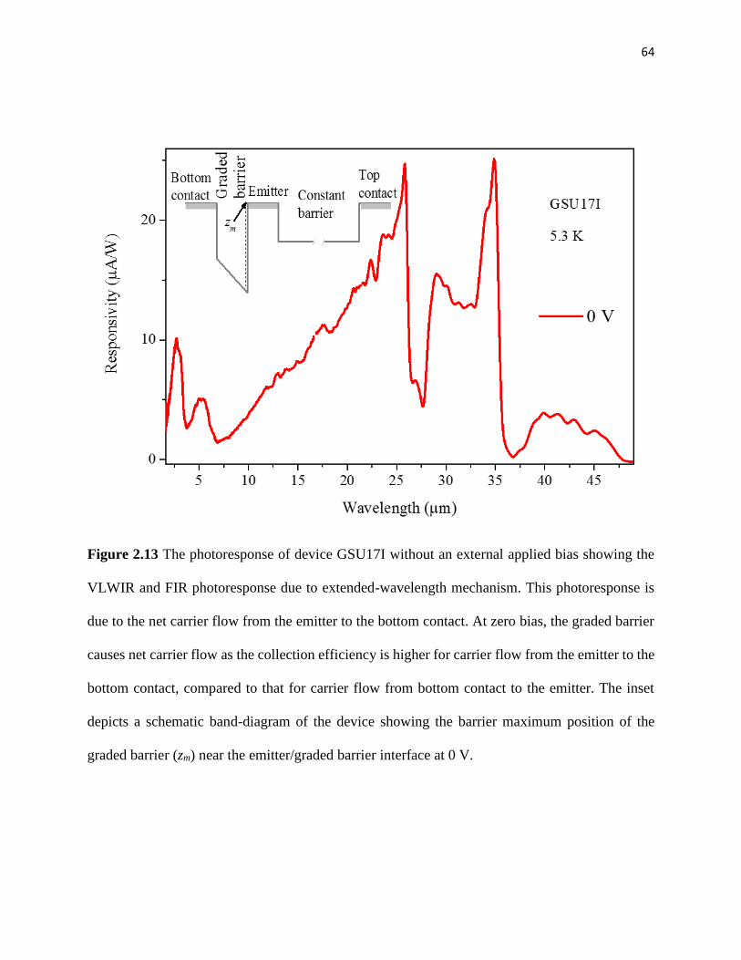
64
Figure 2.13 The photoresponse of device GSU17I without an external applied bias showing the
VLWIR and FIR photoresponse due to extended-wavelength mechanism. This photoresponse is
due to the net carrier flow from the emitter to the bottom contact. At zero bias, the graded barrier
causes net carrier flow as the collection efficiency is higher for carrier flow from the emitter to the
bottom contact, compared to that for carrier flow from bottom contact to the emitter. The inset
depicts a schematic band-diagram of the device showing the barrier maximum position of the
graded barrier (zm) near the emitter/graded barrier interface at 0 V.
65
Figure 2.14 A comparison of the spectral photoresponse of the device GSU17I at 0 V, -0.2 V, and
-0.4 V. The spectral photoresponse at 0 V is from a net carrier flow towards the bottom contact. A
small negative bias (-0.2 V) tends to drive the carriers in the opposite direction, thus reducing the
photoresponse. At -0.4 V, note that there is a notch in the spectral photoresponse near 2.7 µm,
indicating a photocurrent cancellation at this point due to the equal and opposite direction of the
photocurrents. For wavelengths < 2.7 µm, the net photocurrent is still directed towards the bottom
contact. However, for wavelengths > 2.7 µm, the net photocurrent is directed towards the top
contact, which is also evident from the shape change in the spectra beyond ~6 µm compared to
that in the case of 0 V and -0.2 V. Further increase in the negative bias overcomes the cancelation
and leads to stronger photoresponse towards the top contact, as shown in Figure 2.10.
66
enabling the 0 V operation of the IR photodetector.59,60 Thus, at 0 V, there will be a net hot-carrier
flow from the emitter to the bottom contact, which is opposite of the hot-carrier injection.
This fact is further supported by the observed results under low negative biases. For
instance, at -0.2 V, the applied bias tends to drive the carrier flow towards the top contact (opposite
of the net carrier flow at 0 V), thus reducing the photoresponse as shown in Figure 2.14. At a
slightly higher negative bias (-0.4 V) the photoresponse is further reduced. Also, a notch is
noticeable near 2.7 µm, which is an indication that photocurrents due to the IR radiation near 2.7
µm are equal in magnitude but opposite in direction, thus causing the cancellation. For
wavelengths < 2.7 µm, the net photocurrent is still directed towards the bottom contact. However,
for wavelengths > 2.7 µm, the net photocurrent is directed towards the top contact, which is also
evident from the spectral shape change beyond ~6 µm at -0.4 V compared to that in the case of 0V
and -0.2 V. Further increase in the negative bias overcomes the cancelation and leads to stronger
photoresponse towards the top contact, as shown in Figure 2.10.
It is clear at this point that VLWIR and FIR photoresponse is observed even without the
hot-carrier injection from the bottom contact to the emitter. In order to understand the precise
mechanism, it is important to consider two facts for the experimental results. The first is the
disappearance of VLWIR and FIR spectral photoresponse with the use of the long-pass cut-on
filters to block the incident IR radiation in the SWIR and MIR regime, mostly in the < 4 µm range,
indicating that this regime of IR radiation is a critical requirement. The second is that the variation
in the barrier offset energy did not cause any significant alteration in the wavelength threshold,
indicating that the quasi-equilibrium Fermi level is built-up at a certain energy level, which
remains unchanged from device to device.
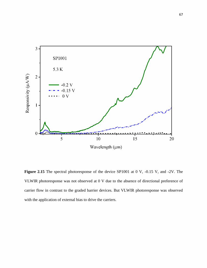
67
Figure 2.15 The spectral photoresponse of the device SP1001 at 0 V, -0.15 V, and -2V. The
VLWIR photoresponse was not observed at 0 V due to the absence of directional preference of
carrier flow in contrast to the graded barrier devices. But VLWIR photoresponse was observed
with the application of external bias to drive the carriers.
68
These facts lead to a situation where the quasi-equilibrium Fermi level is built up in the S-
O band, owing the photo-excitation from L-H/H-H bands to the S-O band. With the λCO = 4.5µm
long-pass cut-on filter, the S-O band transition is not possible. Therefore, the quasi-equilibrium
Fermi level will not be built-up, hence the VLWIR and FIR spectral photoresponse disappears.
However, with the λCO = 2.4 µm long-pass cut-on filter, a portion of the incident IR radiation will
have enough energy for the S-O band transition, which explains the observation of VLWIR and
FIR spectral photoresponse observed with the use of this filter. The S-O band (= 0.34 eV) is a fixed
energy level, thus the quasi-equilibrium remains unchanged from device to device. Furthermore,
the quasi-equilibrium will be built-up not only in the emitter, but also in the bottom and top contact
layers as long as there is photo-excitation to the S-O band. The net flow of the photo-excited
carriers will determine the spectral photoresponse.
The net flow of the photoexcited carriers at 0 V is seen to be directed from the emitter
towards the bottom contact due to the graded barrier. However, the barrier between the emitter and
the top contact has a constant potential profile. This means the collection efficiency over the
constant barrier will remain the same for carrier flow from the emitter to the top contact and vice-
versa. The carrier flow from the emitter to the bottom contact (over the graded barrier) will be
compensated by the carrier flow from the top contact towards the emitter (over the constant
barrier), thus maintaining the photoresponse signal at 0 V. However, in the case of the device
SP1001, absence of the graded barrier will make the net carrier flow unlikely at 0 V. This may be
the reason that a VLWIR photoresponse was not observed at 0 V as shown in Figure 2.15.
However, the VLWIR photoresponse was observed with the application of external bias to drive
the carriers, where the bias also causes the barrier shape change.
69
It is also important to analyze the physical processes in the presence of a non-zero barrier
energy offset (𝛿E >0), since the reference device LH1002 with 𝛿E = 0 did not show the VLWIR
and FIR spectral photoresponse. As explained before, the barrier energy offset is the energy
difference between the bottom and the top barriers. Each of the barrier layers can be considered as
an individual resistor connected in series, with the resistance being a function of applied bias (i.e.,
dynamic resistance) at a given temperature. The differences in the barrier energy will lead to a
non-uniform drop of the applied bias among the two barriers, the higher magnitude of voltage
dropped being across the higher energy barrier. Thus, the non-uniformity in the applied bias
distribution is validated by experimental results.59,61 In addition, the dynamic resistance of the high
energy barrier decreases with increasing applied field. As the dynamic resistance becomes
comparable to that of the low energy barrier, the applied electric field is more uniformly distributed
to the low energy barrier, too. This means, when the applied bias is small, it will drop mostly across
the higher energy barrier, and will be able drive the carrier flow over it. But the effect of the small
applied bias will be much smaller across the low energy barrier. Specifically, in a small bias
regime, the applied bias efficiently drives the carrier flow over the high energy barrier to the
emitter, but the carrier flow will not occur with the same efficiency from the emitter to the top
contact. Therefore, a fraction of a population of photoexcited carriers will be maintained in the
emitter, leading to the quasi-equilibrium Fermi level being built-up. As the applied bias is further
increased to a magnitude high enough to achieve a more uniform field distribution, the photo-
excited carriers in the emitter are easily swept-out, over the top barrier, to be collected at the top
contact. Hence, the quasi-equilibrium Fermi level will not be sustained. The disappearance of the
VLWIR and FIR spectral photoresponse in SP1007 at the applied biases beyond -0.2 V as reported
previously36 can be understood in terms of non-uniform field distribution in the low bias regime.
70
However, with a significant increase in the barrier energy offset (in case of 15SP3 and GSU17I),
the difference between the resistances of the two barriers also increases (exponentially, since 0R
~ )/exp( kT , where 0R is the resistance at 0 V) significantly. Then, the applied bias of a higher
magnitude, compared to that in SP1007, will be needed to approach a uniform field distribution.
This explains the VLWIR and FIR spectral photoresponse of the devices 15SP3 and GSU17I at
considerably higher biases compared to SP1007.
Finally, in case of the device LH1002, the absence of the barrier energy offset (i.e., 𝛿E =
0), causes a uniform field distribution across the both barriers. Therefore, the photo-excited carriers
in the emitter are swept-out over the barrier, to the top contact with negative bias and vice-versa.
This will produce the spectral photoresponse in the SWIR and MIR regime. The VLWIR and FIR
spectral photoresponse was not observed owing to the absence of the quasi-equilibrium Fermi
level.
The implications of these findings will be important towards the future developments of
IR photodetectors, especially with the extended-wavelength mechanism. The study can be
extended to different types of IR photodetectors such as quantum wells infrared photodetectors
(QWIPs) and quantum dots infrared photodetectors (QDIPs). The key to the design of such IR
photodetectors is to find a condition that leads to a quasi-equilibrium Fermi level at a certain energy
level of photo-excitation.
2.4.5 Spectral photoresponse with barrier gradient variation
The set of devices 15SP3, GSU17II, and GSU17III include the gradients of bottom AlxGa1-xAs
barrier of ~20.6, 28.9, and 37.1 kV/cm respectively. These devices have the same values for the
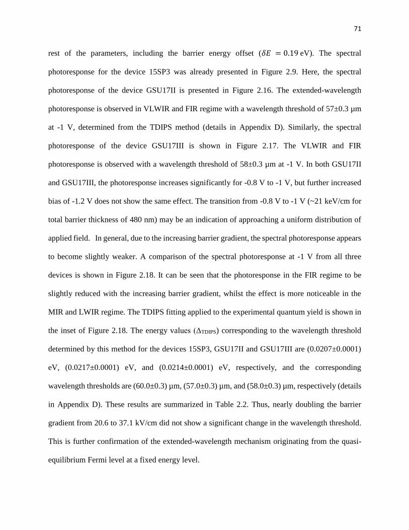
71
rest of the parameters, including the barrier energy offset (𝛿𝐸 = 0.19 eV). The spectral
photoresponse for the device 15SP3 was already presented in Figure 2.9. Here, the spectral
photoresponse of the device GSU17II is presented in Figure 2.16. The extended-wavelength
photoresponse is observed in VLWIR and FIR regime with a wavelength threshold of 57±0.3 µm
at -1 V, determined from the TDIPS method (details in Appendix D). Similarly, the spectral
photoresponse of the device GSU17III is shown in Figure 2.17. The VLWIR and FIR
photoresponse is observed with a wavelength threshold of 58±0.3 µm at -1 V. In both GSU17II
and GSU17III, the photoresponse increases significantly for -0.8 V to -1 V, but further increased
bias of -1.2 V does not show the same effect. The transition from -0.8 V to -1 V (~21 keV/cm for
total barrier thickness of 480 nm) may be an indication of approaching a uniform distribution of
applied field. In general, due to the increasing barrier gradient, the spectral photoresponse appears
to become slightly weaker. A comparison of the spectral photoresponse at -1 V from all three
devices is shown in Figure 2.18. It can be seen that the photoresponse in the FIR regime to be
slightly reduced with the increasing barrier gradient, whilst the effect is more noticeable in the
MIR and LWIR regime. The TDIPS fitting applied to the experimental quantum yield is shown in
the inset of Figure 2.18. The energy values (ΔTDIPS) corresponding to the wavelength threshold
determined by this method for the devices 15SP3, GSU17II and GSU17III are (0.0207±0.0001)
eV, (0.0217±0.0001) eV, and (0.0214±0.0001) eV, respectively, and the corresponding
wavelength thresholds are (60.0±0.3) µm, (57.0±0.3) µm, and (58.0±0.3) µm, respectively (details
in Appendix D). These results are summarized in Table 2.2. Thus, nearly doubling the barrier
gradient from 20.6 to 37.1 kV/cm did not show a significant change in the wavelength threshold.
This is further confirmation of the extended-wavelength mechanism originating from the quasi-
equilibrium Fermi level at a fixed energy level.

72
Figure 2.16 The spectral photoresponse of the device GSU17II at 5.3K showing the the VLWIR
and FIR photoresponse. The wavelength threshold determined by the TDIPS method (details in
Appendix D) is 57±0.3 µm at -1 V. The photoresponse is seen to increase significantly from -0.8
V to -1 V. At -1.2 V, the photoresponse in the MIR and LWIR regime increases, but remains fairly
the same in the rest of the spectrum.
73
Figure 2.17 The spectral photoresponse of the device GSU17III showing the VLWIR and FIR
photoresponse. The wavelength threshold determined by the TDIPS method (details in Appendix
D) is 58±0.3 µm at -1 V. The photoresponse is seen to increase significantly from -0.8 V to -1 V.
At -1.2 V, the photoresponse is only slightly higher compared to -1 V bias voltage.
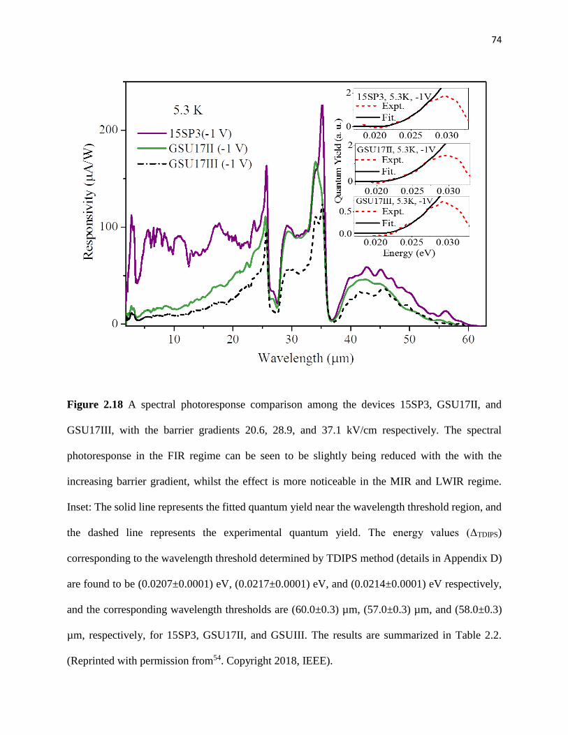
74
Figure 2.18 A spectral photoresponse comparison among the devices 15SP3, GSU17II, and
GSU17III, with the barrier gradients 20.6, 28.9, and 37.1 kV/cm respectively. The spectral
photoresponse in the FIR regime can be seen to be slightly being reduced with the with the
increasing barrier gradient, whilst the effect is more noticeable in the MIR and LWIR regime.
Inset: The solid line represents the fitted quantum yield near the wavelength threshold region, and
the dashed line represents the experimental quantum yield. The energy values (ΔTDIPS)
corresponding to the wavelength threshold determined by TDIPS method (details in Appendix D)
are found to be (0.0207±0.0001) eV, (0.0217±0.0001) eV, and (0.0214±0.0001) eV respectively,
and the corresponding wavelength thresholds are (60.0±0.3) µm, (57.0±0.3) µm, and (58.0±0.3)
µm, respectively, for 15SP3, GSU17II, and GSUIII. The results are summarized in Table 2.2.
(Reprinted with permission from54. Copyright 2018, IEEE).
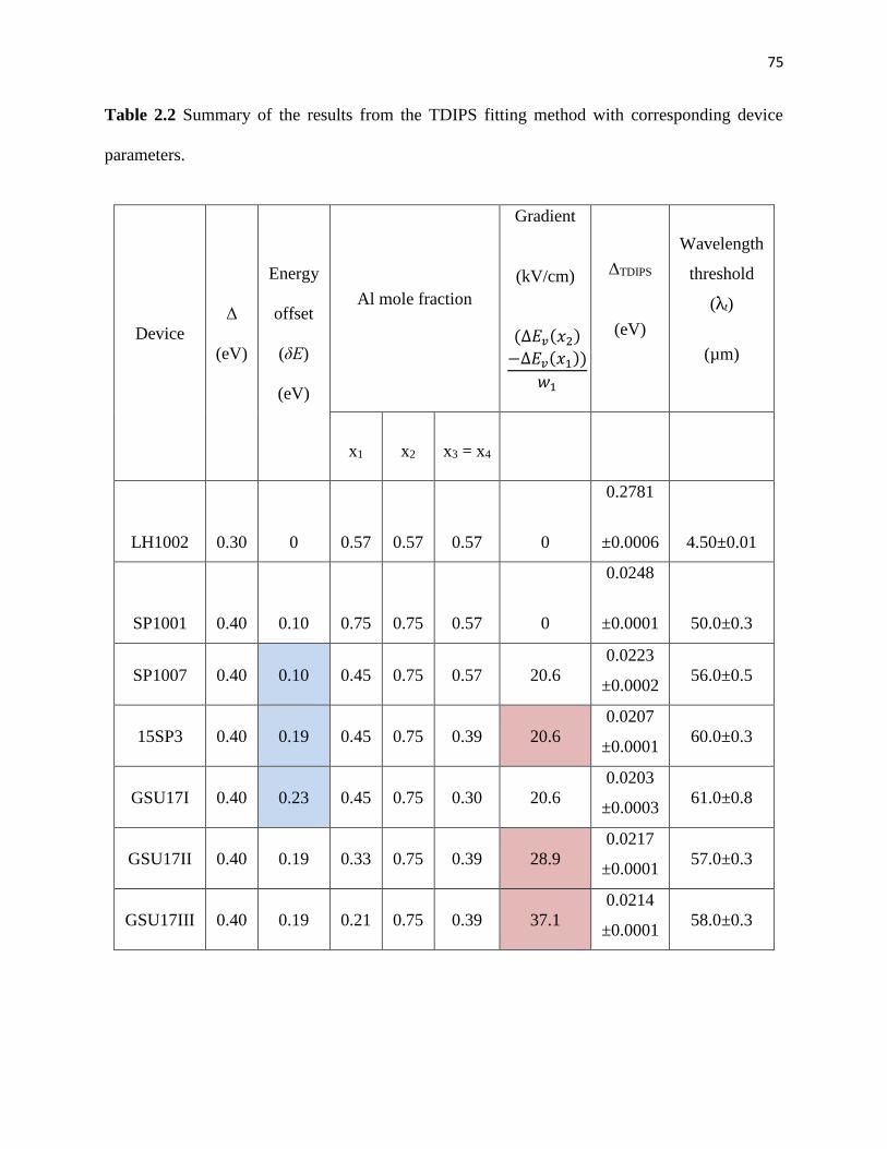
75
Table 2.2 Summary of the results from the TDIPS fitting method with corresponding device
parameters.
Device
Δ
(eV)
Energy
offset
(δE)
(eV)
Al mole fraction
Gradient
(kV/cm)
(∆𝐸𝑣(𝑥2)
−∆𝐸𝑣(𝑥1))
𝑤1
ΔTDIPS
(eV)
Wavelength
threshold
(λt)
(µm)
x1 x2 x3 = x4
LH1002 0.30 0 0.57 0.57 0.57 0
0.2781
±0.0006 4.50±0.01
SP1001 0.40 0.10 0.75 0.75 0.57 0
0.0248
±0.0001 50.0±0.3
SP1007 0.40 0.10 0.45 0.75 0.57 20.6
0.0223
±0.0002 56.0±0.5
15SP3 0.40 0.19 0.45 0.75 0.39 20.6
0.0207
±0.0001 60.0±0.3
GSU17I 0.40 0.23 0.45 0.75 0.30 20.6
0.0203
±0.0003 61.0±0.8
GSU17II 0.40 0.19 0.33 0.75 0.39 28.9
0.0217
±0.0001 57.0±0.3
GSU17III 0.40 0.19 0.21 0.75 0.39 37.1
0.0214
±0.0001 58.0±0.3
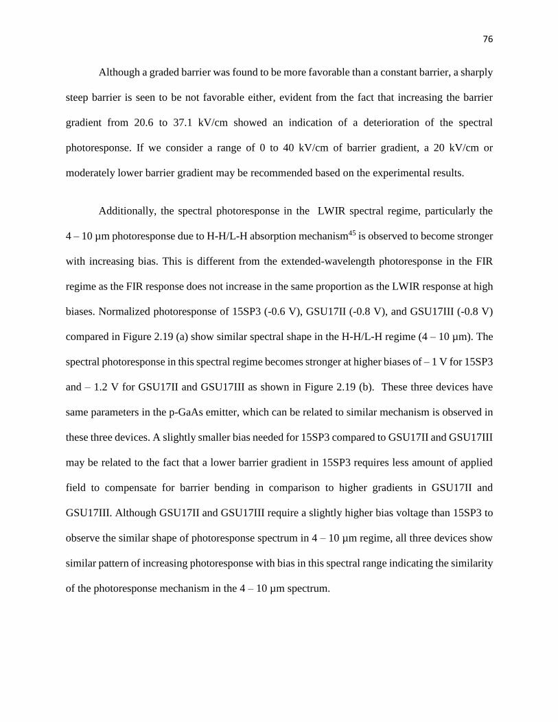
76
Although a graded barrier was found to be more favorable than a constant barrier, a sharply
steep barrier is seen to be not favorable either, evident from the fact that increasing the barrier
gradient from 20.6 to 37.1 kV/cm showed an indication of a deterioration of the spectral
photoresponse. If we consider a range of 0 to 40 kV/cm of barrier gradient, a 20 kV/cm or
moderately lower barrier gradient may be recommended based on the experimental results.
Additionally, the spectral photoresponse in the LWIR spectral regime, particularly the
4 – 10 µm photoresponse due to H-H/L-H absorption mechanism45 is observed to become stronger
with increasing bias. This is different from the extended-wavelength photoresponse in the FIR
regime as the FIR response does not increase in the same proportion as the LWIR response at high
biases. Normalized photoresponse of 15SP3 (-0.6 V), GSU17II (-0.8 V), and GSU17III (-0.8 V)
compared in Figure 2.19 (a) show similar spectral shape in the H-H/L-H regime (4 – 10 µm). The
spectral photoresponse in this spectral regime becomes stronger at higher biases of – 1 V for 15SP3
and – 1.2 V for GSU17II and GSU17III as shown in Figure 2.19 (b). These three devices have
same parameters in the p-GaAs emitter, which can be related to similar mechanism is observed in
these three devices. A slightly smaller bias needed for 15SP3 compared to GSU17II and GSU17III
may be related to the fact that a lower barrier gradient in 15SP3 requires less amount of applied
field to compensate for barrier bending in comparison to higher gradients in GSU17II and
GSU17III. Although GSU17II and GSU17III require a slightly higher bias voltage than 15SP3 to
observe the similar shape of photoresponse spectrum in 4 – 10 µm regime, all three devices show
similar pattern of increasing photoresponse with bias in this spectral range indicating the similarity
of the photoresponse mechanism in the 4 – 10 µm spectrum.

77
Figure 2.19 (a) A comparison of normalized photoresponse in the of 15SP3 (-0.6 V), GSU17II (-
0.8 V), and GSU17III (-0.8 V) showing similar spectral shape in the H-H/L-H regime (4 – 10 µm).
(b) The spectral photoresponse becomes stronger at higher biases of – 1 V for 15SP3 and -1.2 V
GSU17II and GSU17III. Similar mechanism is observed in these three devices, with slightly
smaller bias needed for 15SP3 compared to GSU17II and GSU17III.
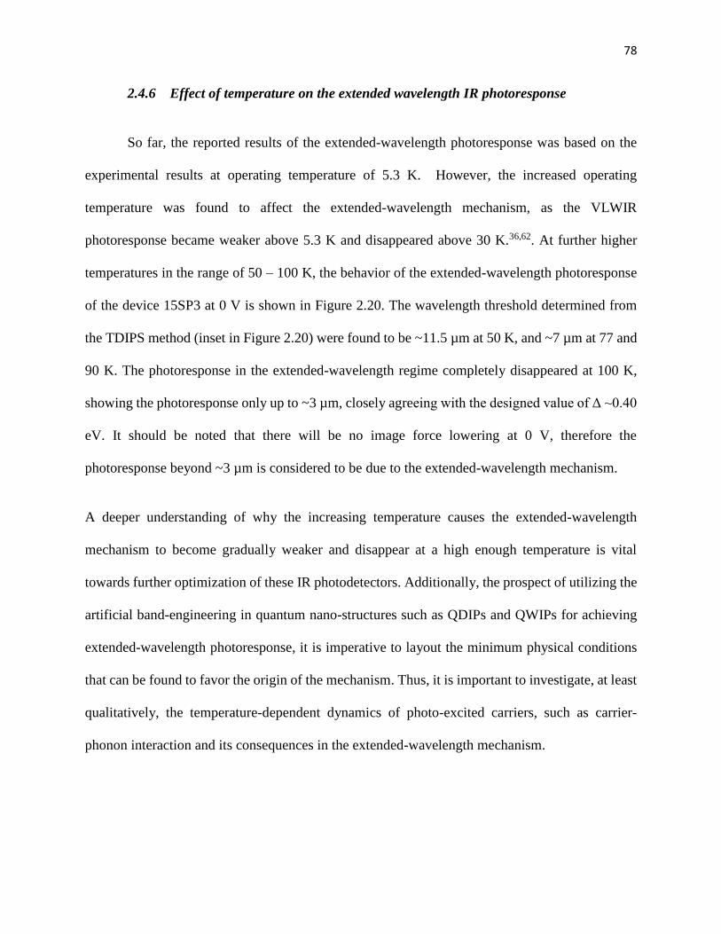
78
2.4.6 Effect of temperature on the extended wavelength IR photoresponse
So far, the reported results of the extended-wavelength photoresponse was based on the
experimental results at operating temperature of 5.3 K. However, the increased operating
temperature was found to affect the extended-wavelength mechanism, as the VLWIR
photoresponse became weaker above 5.3 K and disappeared above 30 K.36,62. At further higher
temperatures in the range of 50 – 100 K, the behavior of the extended-wavelength photoresponse
of the device 15SP3 at 0 V is shown in Figure 2.20. The wavelength threshold determined from
the TDIPS method (inset in Figure 2.20) were found to be ~11.5 µm at 50 K, and ~7 µm at 77 and
90 K. The photoresponse in the extended-wavelength regime completely disappeared at 100 K,
showing the photoresponse only up to ~3 µm, closely agreeing with the designed value of Δ ~0.40
eV. It should be noted that there will be no image force lowering at 0 V, therefore the
photoresponse beyond ~3 µm is considered to be due to the extended-wavelength mechanism.
A deeper understanding of why the increasing temperature causes the extended-wavelength
mechanism to become gradually weaker and disappear at a high enough temperature is vital
towards further optimization of these IR photodetectors. Additionally, the prospect of utilizing the
artificial band-engineering in quantum nano-structures such as QDIPs and QWIPs for achieving
extended-wavelength photoresponse, it is imperative to layout the minimum physical conditions
that can be found to favor the origin of the mechanism. Thus, it is important to investigate, at least
qualitatively, the temperature-dependent dynamics of photo-excited carriers, such as carrier-
phonon interaction and its consequences in the extended-wavelength mechanism.

79
Figure 2.20 Spectral photoresponse of the photodetector 15SP3 at 0 V, in the temperature range
50 – 100K. The extended wavelength threshold was observed to be ~11.5 µm at 50K, and ~7 µm
at 77K and 90K. The photoresponse in the extended-wavelength region disappeared at 100K, and
the threshold of ~3 µm then closely agrees with the designed value of Δ ~0.40 eV. Inset: TDIPS
fittings of the experimental quantum yield spectra to determine the wavelength threshold.
(Reprinted with permission from38. Copyright 2017, AIP Publishing).
80
The carrier-phonon dynamics will be discussed here, in order to set a path forward to design
a most promising IR photodetector with extended-wavelength mechanism.
Photo-excitation or application of a strong electric field causes the carriers (electrons,
holes, or both) to become ‘hot’ relative to their surroundings. The dominant mechanism of energy-
relaxation process (or thermalization) is through longitudinal-optical (LO) phonon emission,57
even though transverse-optical (TO) phonon emission may follow at a delayed time scale63. A high
phonon emission rate in the presence of a high hot-carrier population sends the phonon population
into a non-equilibrium condition, consequentially slowing down the energy-relaxation of hot-
carriers, the effect being referred to as the hot-phonon bottleneck effect.64-66 The hot-carrier
energy-relaxation rate is very fast in the bulk (3D) material, hence a very short carrier lifetime, for
instance, ~1 picosecond in GaAs.67 Furthermore, the phonon bottleneck effect has been studied in
the low dimensional structures, such as in quantum wells65,68 (2D), quantum nanowires56,57 (1D),
and quantum dots69-71 (0D).
The reduced dimensionality leads to energy level quantization. This causes an energy
mismatch between the LO phonons and the hot-carriers, hence slows down the phonon emission
rate. Experimental results demonstrated the hot-carrier cooling slowed down by hundreds of
picoseconds in the high carrier density (>1018 cm-3) regime in quantum wells68. Furthermore,
remarkably long carrier lifetimes in quantum dots, in nanosecond-scale, have been recently
reported.69,70 Besides III-V semiconductors, the phonon-bottleneck effect was found to slow down
the hot carrier cooling by three orders of magnitude in the high carrier density regime of ≥6×10¹⁸
cm-3 in lead-iodide perovskites.72 An obvious advantage of the slower hot-carrier cooling in

81
optoelectronic devices, such as solar cells, would be an improved carrier extraction increasing the
efficiency73.
LO phonon energy ( LO ) is ~0.036 eV for GaAs.74 Their occupation number under
equilibrium at a temperature T is given by
1exp
1
−
=
kT
nLO
(2.2)
A temperature-dependence of the occupation number (see Appendix F) shows a dramatic variation
from ~0.042 at 100 K to be practically non-existent at 5.3 K. This is a fundamental material
property and provides a qualitative indication of how easily the phonon population can become
non-equilibrium at very low temperatures such as 5.3 K and hence lead to the phonon bottleneck
effect.
Evidently, the phonon bottleneck effect is the underlying reason that the energy-relaxation
rate of the photoexcited carriers is slow enough to maintain a quasi-equilibrium Fermi level near
the S-O band and enable the extended-wavelength mechanism at very low temperatures. However,
the dramatic temperature-dependence of the phonon occupation number may be related to the
weakening and subsequent disappearance of the VLWIR photoresponse when temperature is
increased above 5.3 K.
82
2.5 Future Work
Based on the results and discussion in the previous section, two fundamental requirements
can be outlined, in order to observe an extended-wavelength photoresponse in an IR photodetector:
1. Carriers should be photo-excited from a low energy level (ground state) to a higher
energy state. In future studies, a laser source of suitable wavelength may be the
most appropriate option. The process may be referred to as ‘pumping’.
2. A hot-phonon bottleneck effect must be present in order to maintain a quasi-
equilibrium Fermi level at the higher energy state.
The first requirement can be met fairly easily, for example, by using an intrinsic III-V
semiconductor with a suitable band-gap (Eg), such as InAs (Eg = 0.354 eV; 3.5 µm). p-type III-V
semiconductors may also be used with a suitable S-O band energy. In fact, the p-GaAs has been
used exclusively and extensively in this work.
However, the second requirement is more challenging to satisfy, especially when the bulk
material is used. The stringent requirement of a very low temperature to achieve a phonon
bottleneck effect may not be in the best interest of different applications that use IR photodetector
and imaging systems. In general, the operating temperature of the IR photodetectors (photon-
detector type) depends on their spectral regime; for example, a LWIR or longer wavelength range
requires cooling, typically 77 K or lower. On the other hand, the MIR photodetectors operate at
some elevated temperatures of 100 – 200 K, depending on the properties of the absorbing material,
and device architecture. Therefore, in order to exploit fully the advantage of wavelength-extension
mechanism, a careful choice of device design (bulk versus low dimensional) is necessary. Further
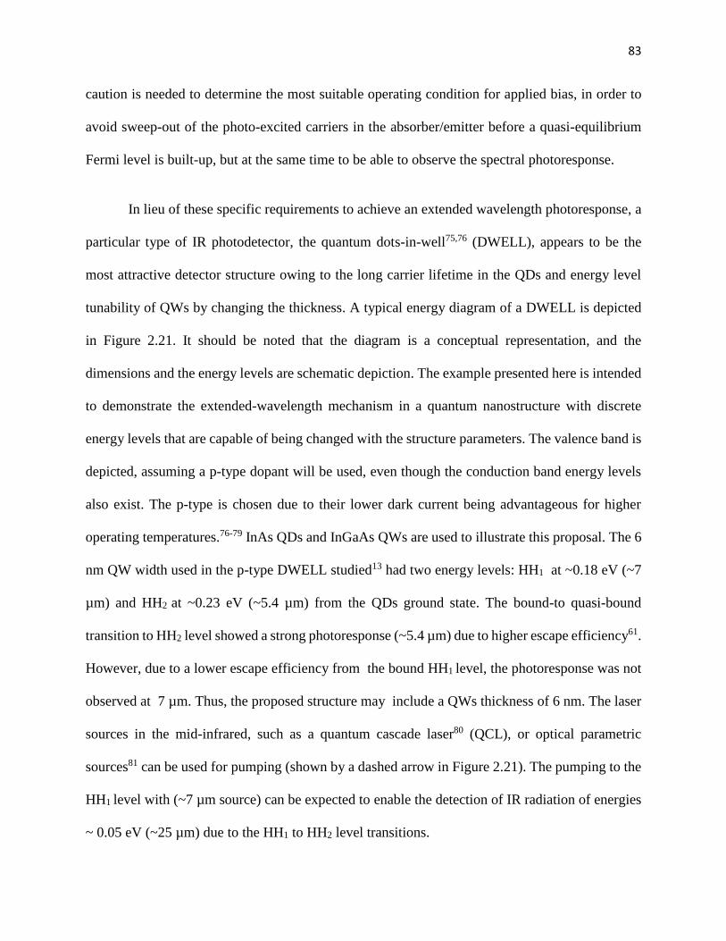
83
caution is needed to determine the most suitable operating condition for applied bias, in order to
avoid sweep-out of the photo-excited carriers in the absorber/emitter before a quasi-equilibrium
Fermi level is built-up, but at the same time to be able to observe the spectral photoresponse.
In lieu of these specific requirements to achieve an extended wavelength photoresponse, a
particular type of IR photodetector, the quantum dots-in-well75,76 (DWELL), appears to be the
most attractive detector structure owing to the long carrier lifetime in the QDs and energy level
tunability of QWs by changing the thickness. A typical energy diagram of a DWELL is depicted
in Figure 2.21. It should be noted that the diagram is a conceptual representation, and the
dimensions and the energy levels are schematic depiction. The example presented here is intended
to demonstrate the extended-wavelength mechanism in a quantum nanostructure with discrete
energy levels that are capable of being changed with the structure parameters. The valence band is
depicted, assuming a p-type dopant will be used, even though the conduction band energy levels
also exist. The p-type is chosen due to their lower dark current being advantageous for higher
operating temperatures.76-79 InAs QDs and InGaAs QWs are used to illustrate this proposal. The 6
nm QW width used in the p-type DWELL studied13 had two energy levels: HH1 at ~0.18 eV (~7
µm) and HH2 at ~0.23 eV (~5.4 µm) from the QDs ground state. The bound-to quasi-bound
transition to HH2 level showed a strong photoresponse (~5.4 µm) due to higher escape efficiency61.
However, due to a lower escape efficiency from the bound HH1 level, the photoresponse was not
observed at 7 µm. Thus, the proposed structure may include a QWs thickness of 6 nm. The laser
sources in the mid-infrared, such as a quantum cascade laser80 (QCL), or optical parametric
sources81 can be used for pumping (shown by a dashed arrow in Figure 2.21). The pumping to the
HH1 level with (~7 µm source) can be expected to enable the detection of IR radiation of energies
~ 0.05 eV (~25 µm) due to the HH1 to HH2 level transitions.
84
Figure 2.21 A schematic of a proposed design for the extended-wavelength IR photodetector
based on quantum dots-in-a-well (DWELL) structure. A laser source can be used for photo-
excitation from the ground state energy level in the QDs to an energy level in the QW (shown by
a dashed arrow) to form a quasi-equilibrium Fermi level. Then, the background IR radiation can
be detected due to transitions from the quasi-equilibrium to higher QW levels (shown by solid
arrows). A QW thickness of 6 nm, similar to that reported previously,13 will have two energy
levels: HH1 at ~0.18 eV (~7 µm) and HH2 at ~0.23 eV (~5.4 µm) from the QDs ground state. The
pumping to the HH1 level with (~7 µm source) can be expected to enable the detection of IR
radiation of energies ~ 0.05 eV (~25 µm) due to HH1 to HH2 transitions. A high energy (graded)
barrier is used to ensure an applied bias will not easily sweep-out carriers from the quasi-
equilibrium Fermi level.
85
These energy levels can also be changed by using different well thicknesses; for instance, reducing
the QW thickness will increase the separation between the energy levels. A GaAs barrier is used
on the collector side, whilst a graded AlxGa1-xAs high energy barrier is used on the injector side.
The commonly used thicknesses for the barriers76,77 are in the range of 60 – 80 nm, which can be
adopted in this proposed structure as well. A high energy (graded) barrier is used to ensure an
applied bias will not easily sweep-out carriers from the quasi-equilibrium Fermi level.
A specific spectral band detection, particularly the 3 – 5 µm detection, may be more
challenging due to the fact that the difference between HH1 and HH2 energy levels in the
InAs/InGaAs/GaAs DWELL structure are not large enough. However, recently reported77 results
on p-type InAs/GaAs QDIPs showed a weak photoresponse near 2.3 µm due to the ground state
to SO band (~0.52 eV) transition. The photoresponse was weak due to the fact that the S-O band
lies in the continuum. In order to make the SO level a bound state, the GaAs barrier can be replaced
with an AlGaAs (or AlAs) barrier. Then, the energy difference of 0.29 eV (~4.3 µm) between the
HH2 and SO levels can be highly suitable for the 3 – 5 µm band detection. A schematic of a possible
DWELL structure for 3 – 5 µm band detection is depicted in Figure 2.22. Pumping to the HH2
level will require a 5.4 µm laser source. Unlike the IR detection due to SO band transitions by
using the bulk (3D) materials, the DWELL structures will have the advantage of long carrier
lifetime. Therefore, the phonon bottleneck effect can be expected to be maintained at higher
temperatures due to the significantly larger HH2 energy level (~0.23eV) compared to the InAs LO
phonon energy (0.029 eV).
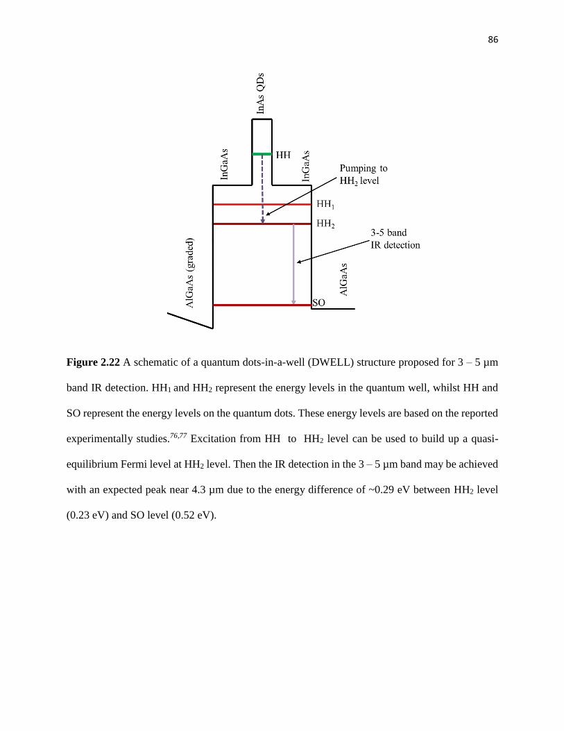
86
Figure 2.22 A schematic of a quantum dots-in-a-well (DWELL) structure proposed for 3 – 5 µm
band IR detection. HH1 and HH2 represent the energy levels in the quantum well, whilst HH and
SO represent the energy levels on the quantum dots. These energy levels are based on the reported
experimentally studies.76,77 Excitation from HH to HH2 level can be used to build up a quasi-
equilibrium Fermi level at HH2 level. Then the IR detection in the 3 – 5 µm band may be achieved
with an expected peak near 4.3 µm due to the energy difference of ~0.29 eV between HH2 level
(0.23 eV) and SO level (0.52 eV).
87
There are several advantages of using the DWELL architecture over other possibilities.
The energy levels in QWs can be tuned to achieve the most suitable combination of the levels for
extended-wavelength mechanism. The highest energy level in the QW can be set to bound or
continuum, without altering the ground state QDs levels. Furthermore, the intensity of the external
laser used for pumping may also be separately tailored to a high intensity, if necessary, to maintain
a high photo-excited carrier population to sustain the phonon bottleneck effect. As a matter of fact,
the review of the published reports presented in the previous section strongly indicates that the
phonon bottleneck effect is stronger at higher densities of photo-excited carriers. Thus, the ability
to tune the pumping separately is also an important feature.
This structure will also benefit from the long carrier lifetime in QDs. The energy gap
between the ground state in QDs and an excited state in the QW should be much higher than the
LO phonon energy of InAs (~0.029 eV), which can be achieved by choosing a suitable well width.
Due to the energy quantization, the energy-relaxation to the ground state will be possible only with
multi-phonon emission66,76 to match the energy difference, essentially slowing down the relaxation
process. Since the pumping can be controlled separately, a high density of photo-excited carriers
can be maintained to sustain the phonon bottleneck effect. It should be noted, however, that the
photo-excited carriers due to the laser can cause a higher dc current through the device. This can
be overcome by using a pulsed laser, and the pulsing frequency being suitably synchronized
(possibly in the multiples in terms of numbers) with the read-out frequency of the focal plane
arrays.
88
The DWELL is preferred due to its sensitivity to normal incidence of the IR radiation
unlike the n-type QWIPs. Furthermore, in the p-type DWELL, the higher effective mass of the
holes compared to the electrons enables densely packed energy levels near continuum,76 thus a
broader spectral response can be observed. The higher effective mass also makes the holes less
sensitive to thermionic emission compared to electrons, therefore p-type structure is preferable
since a higher operating temperature is also the goal.
Besides the experimental aspects of the design, there will be more questions that need
answers, for example, the optimized pumping, optimized barrier height and applied bias to enable
measurement of the photoresponse without severe sweep-out, and so on. Furthermore, it may be
possible that a high pumping intensity can compensate for the effect of temperature on the phonon
bottleneck effect to some extent. Therefore, along with the experimental study, a theoretical study
of hot-carrier and phonon dynamics, and carrier transport under applied field non-uniformity
across the structure, will be necessary.
2.6 Summary
In this Chapter, a detailed experimental study of extended-wavelength IR photodetectors
has been presented. p-GaAs/AlxGa1-xAs heterostructure-based IR photodetectors, with non-zero
barrier energy offset, were used. The detectors had conventional wavelength thresholds of ~3 µm,
corresponding to Δ ~0.4 eV of p-GaAs/AlxGa1-xAs heterostructures. However, with a barrier
energy offset, an extended-wavelength photoresponse was observed up to ~50 µm (in SP1001,
constant barrier device). With the graded barriers and the offset, the extended-wavelength
photoresponse was observed with a slightly longer wavelength threshold, 56, 60 and 61 µm (in
SP1007, 15SP3, GSU17I, respectively). The wavelength threshold of the extended-wavelength

89
photoresponse showed a very small variation (~0.002 eV, from 56 µm to 61 µm) whilst the barrier
energy offset was changed by ~0.13 eV. Instead, increasing the barrier energy led to increased
spectral photoresponse strength. Similarly, increasing the barrier gradient caused no significant
change in the wavelength threshold. However, the spectral photoresponse was observed to become
weaker. These strongly indicated that the quasi-equilibrium Fermi level is at a fixed level,
irrespective of the device parameter: S-O band being the most probable energy level. Analysis of
the observed results suggested that the hot-phonon bottleneck is the underlying cause of the
extended-wavelength mechanism. An extended-wavelength IR photodetector is proposed, based
on DWELL structure, which appears to be the most attractive option due to its flexibility in energy
level tuning, and it is relatively easy to achieve and maintain the hot-phonon bottleneck effect. A
laser source may be used to photo-excite the carriers and tuning the carrier density with the laser
intensity is expected to enhance significantly the extended-wavelength mechanism.
90
3 DARK CURRENT CHARACTERISTICS OF EXTENDED WAVELENGTH
PHOTODETECTORS
3.1 Introduction
The extended-wavelength mechanism enables to overcome the Δ-dependence of the
wavelength threshold set by equation 2.1. However, it is also necessary to study the Δ-dependence
of the dark current in order to understand fully the advantages of the mechanism. It is clear from
the experimental results in the Chapter 2 that the extended-wavelength mechanism is exclusively
an IR radiation-induced phenomenon, in particular the IR radiation with enough energy to cause a
S-O band transition. Therefore, under the dark conditions, the physical properties of the devices
are expected to be unaffected, hence the Δ-dependence of the dark current is expected to agree
with the designed value of Δ for each of the devices. In general, the dark current and the related
noise level of a photoconductive IR detector is dependent on the Δ of the device, in addition to the
other physical properties such as mobility, at a given temperature. A relatively smaller Δ and
corresponding longer spectral wavelengths of a photodetectors would inevitably have a higher dark
current. Therefore, it is important that the dark current of the device is not significantly
compromised due to the extended-wavelength mechanism discussed before.
Two p-GaAs/ AlxGa1-xAs heterostructure devices, LH1002 and 15SP3 (details in Table 2.1
in Chapter 2.2), were used for the study. In addition to the spectral photoresponse characteristics,
LH1002 also serves as a reference device to study the dark current characteristics, due to its
symmetric design in terms of the shape of the AlxGa1-xAs barriers and absence of a barrier energy
offset. The experimentally measured dark current in the temperature range 10 – 100 K was

91
compared with the calculated fitting curves at the respective temperatures. The results were
published in Journal of Applied Physics38.
3.1.1 3D Carrier Drift Model of Dark Current
A 3D carrier drift model,44 given by the relation:
)(3
FvAepIDdark
= (3.1)
Here, A is the electrically active area of the detector, e is the electronic charge, Dp3 is the
thermally-excited carrier (hole) density on the top of the barrier, and )(Fv is the hole drift velocity
as function of applied field F . Using Dp3 and )(Fv given by44
−
=
Tk
ETkmp
B
actB
D exp2
2
2/3
2
*
3
, (3.2)
and 2/1
2
1
)(
+
=
satv
F
FFv
, (3.3)
eq. (3.1) reduces to the familiar form: 30,44
−−−
+
=Tk
EFTkm
v
F
FAeI
B
fB
sat
dark
exp
22
1
2/3
2
*
2/12
. (3.4)
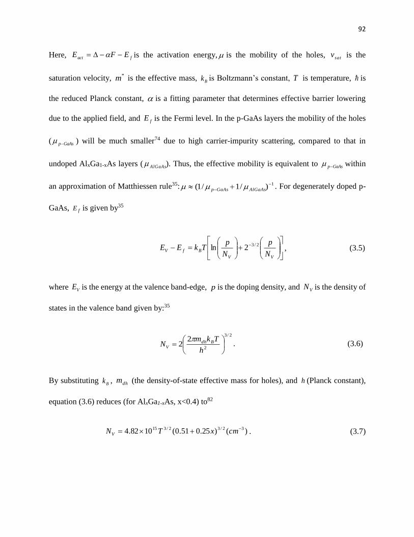
92
Here, fact EFE −−= is the activation energy, is the mobility of the holes, satv is the
saturation velocity, *m is the effective mass,
Bk is Boltzmann’s constant, T is temperature, is
the reduced Planck constant, is a fitting parameter that determines effective barrier lowering
due to the applied field, and fE is the Fermi level. In the p-GaAs layers the mobility of the holes
( GaAsp− ) will be much smaller74 due to high carrier-impurity scattering, compared to that in
undoped AlxGa1-xAs layers ( AlGaAs ). Thus, the effective mobility is equivalent to GaAsp− within
an approximation of Matthiessen rule35: 1)/1/1(−
− + AlGaAsGaAsp . For degenerately doped p-
GaAs, fE is given by35
+
=−
−
VV
BfVN
p
N
pTkEE
2/32ln , (3.5)
where VE is the energy at the valence band-edge, p is the doping density, and VN is the density of
states in the valence band given by:35
2/3
2
22
=
h
TkmN Bdh
V
. (3.6)
By substituting Bk , dhm (the density-of-state effective mass for holes), and h (Planck constant),
equation (3.6) reduces (for AlxGa1-xAs, x<0.4) to82
)()25.051.0(1082.432/32/315 −
+= cmxTNV . (3.7)

93
Since both structures (LH1002 and 15SP3) consist of p-GaAs doped to the same level, the same
values of and satv were used at a given temperature. At a doping density of 1×1019 cm-3,
~50cm2/Vs at room temperature, and an empirical temperature dependence is given74 as:
15.1
21
3.2
3 300104
300105.2)(
−
−−
+
=
Tp
TT (cm2/V s). (3.8)
Similarly, satv ~107 cm/s at room temperature, and an empirical temperature dependence is given83
as:
300)1(
)(300,
TAA
vTv
Ksat
sat
+−
= (cm/s), (3.9)
with A = 0.59 for p-GaAs.83 Finally, is the parameter used to obtain the fitting of the dark
current curves at each temperature.
3.2 Results and Discussion
The measured dark current of the photodetector LH1002 is shown in Figure 3.1,
represented by the dashed lines, and the fittings obtained for the model are represented by the solid
lines in the temperature range of 10 – 100K. The inset in Figure 3.1 shows the fitting parameter
. A constant value of the parameter (~18 nm) was used to fit the dark current for a HEWIP
device30 that operated in a very small range of applied electric field (<1 kV/cm). However, the
devices used in this study operate at 10-100 times higher applied electric fields. Therefore a
variation in the value of was needed to fit the dark currents, particularly at low temperatures
and biases. Noticeably, the parameter had a constant value (~ 8 nm) with the bias at 100 K .
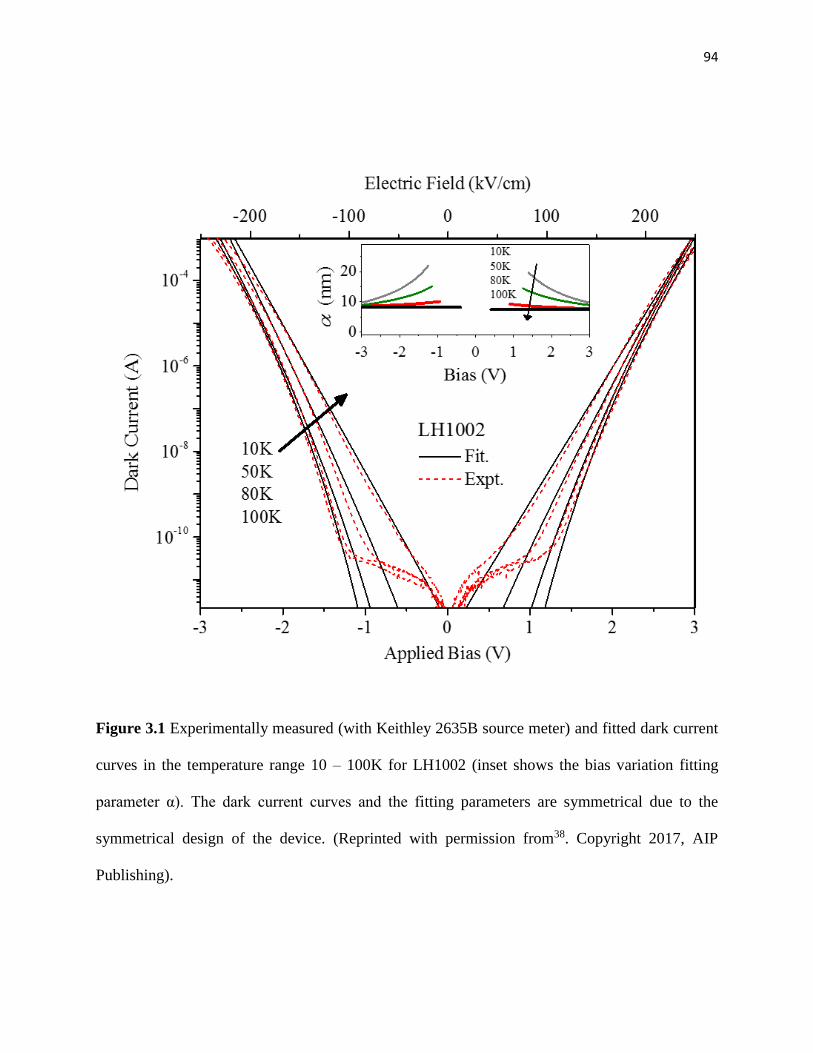
94
Figure 3.1 Experimentally measured (with Keithley 2635B source meter) and fitted dark current
curves in the temperature range 10 – 100K for LH1002 (inset shows the bias variation fitting
parameter α). The dark current curves and the fitting parameters are symmetrical due to the
symmetrical design of the device. (Reprinted with permission from38. Copyright 2017, AIP
Publishing).
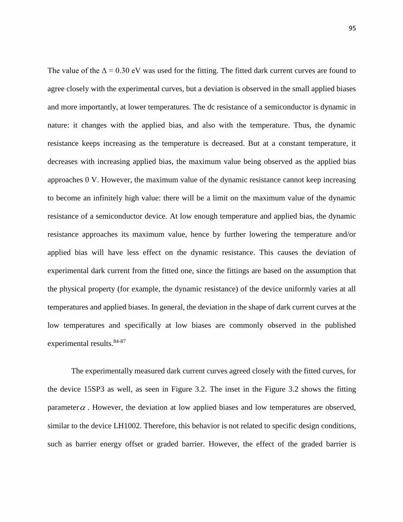
95
The value of the Δ = 0.30 eV was used for the fitting. The fitted dark current curves are found to
agree closely with the experimental curves, but a deviation is observed in the small applied biases
and more importantly, at lower temperatures. The dc resistance of a semiconductor is dynamic in
nature: it changes with the applied bias, and also with the temperature. Thus, the dynamic
resistance keeps increasing as the temperature is decreased. But at a constant temperature, it
decreases with increasing applied bias, the maximum value being observed as the applied bias
approaches 0 V. However, the maximum value of the dynamic resistance cannot keep increasing
to become an infinitely high value: there will be a limit on the maximum value of the dynamic
resistance of a semiconductor device. At low enough temperature and applied bias, the dynamic
resistance approaches its maximum value, hence by further lowering the temperature and/or
applied bias will have less effect on the dynamic resistance. This causes the deviation of
experimental dark current from the fitted one, since the fittings are based on the assumption that
the physical property (for example, the dynamic resistance) of the device uniformly varies at all
temperatures and applied biases. In general, the deviation in the shape of dark current curves at the
low temperatures and specifically at low biases are commonly observed in the published
experimental results.84-87
The experimentally measured dark current curves agreed closely with the fitted curves, for
the device 15SP3 as well, as seen in Figure 3.2. The inset in the Figure 3.2 shows the fitting
parameter . However, the deviation at low applied biases and low temperatures are observed,
similar to the device LH1002. Therefore, this behavior is not related to specific design conditions,
such as barrier energy offset or graded barrier. However, the effect of the graded barrier is
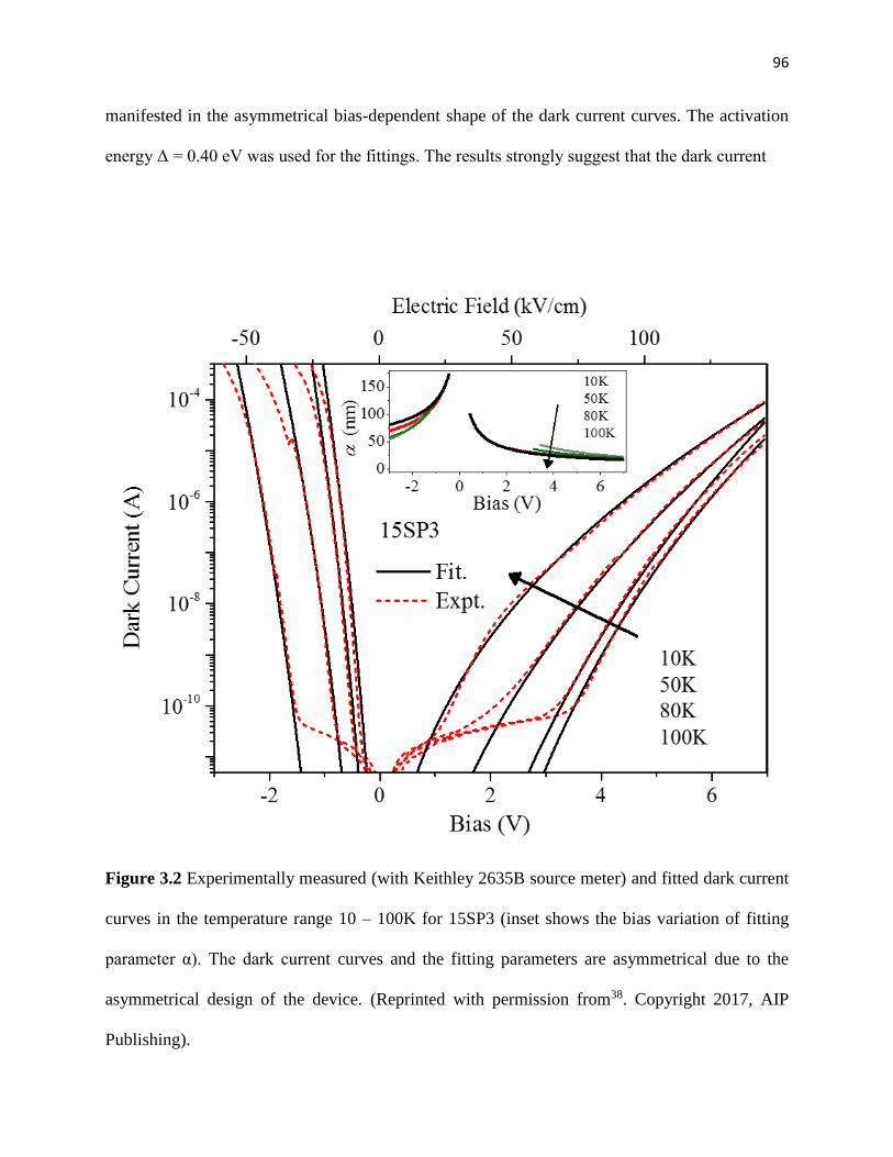
96
manifested in the asymmetrical bias-dependent shape of the dark current curves. The activation
energy Δ = 0.40 eV was used for the fittings. The results strongly suggest that the dark current
Figure 3.2 Experimentally measured (with Keithley 2635B source meter) and fitted dark current
curves in the temperature range 10 – 100K for 15SP3 (inset shows the bias variation of fitting
parameter α). The dark current curves and the fitting parameters are asymmetrical due to the
asymmetrical design of the device. (Reprinted with permission from38. Copyright 2017, AIP
Publishing).
97
Figure 3.3 Spectral photoresponse of 15SP2 and LH1002 as a function of wavelength. At 50K, a
wavelength threshold of ~5.5 µm and dark current value ~2×10⁻⁹ A (Inset) were observed in
LH1002 at -1.5 V. The extended wavelength threshold of 15SP3 at -1 V is significantly longer, up
to ~13.5 µm, but the dark current at this bias is still similar to the dark current in the LH1002 (the
dark current at the respective biases are marked by arrows). (Reprinted with permission from38.
Copyright 2017, AIP Publishing).

98
levels are always determined by the Δ corresponding to the heterojunction parameters, even though
the photoresponse characteristics at particular temperatures defy the limit set by Δ due to extended-
wavelength mechanism. Thus, the dark current was not found to be compromised in the IR
photodetector with the extended-wavelength mechanism.
In order to further illustrate the dark current advantage of the IR photodetector with the
extended-wavelength mechanism, the photoresponse of LH1002 (without the offset) and 15SP3
(with offset) at 50K are shown at biases of -1.5 V and -1V, respectively in Figure 3.3. At these
biases, the dark currents of the two detectors are close to each other (~2×10⁻⁹A, as indicated by the
arrows in the Inset). However, the photoresponse of 15SP3, with the wavelength threshold
extension, is observed up to ~13.5 µm, which is significantly longer compared to the wavelength
threshold of ~5.5 µm for LH1002. It should be noted that there is a small increase in the wavelength
threshold of LH1002, compared to its designed value, due to image force effects.35 The importance
of the wavelength threshold extension mechanism is thus clearly illustrated, with its application
for future IR photodetector design and development.
Furthermore, the experimentally measured dark current of other devices (SP1001, SP1007,
GSU17I, GSU17II, and GSU17III) were also fitted following the same process. It should be noted
that the designed value of the Δ had the same value (~0.4 eV) as in the case of 15SP3. Therefore,
Δ ~0.4 eV was used in the fitting of the dark current of these devices. In addition, Arrhenius plots
were used to obtain activation energy of these devices. The dark current fittings of the devices
SP1001, SP1007, GSU17I, GSU17II, and GSU17III are shown in Figure 3.4, 3.6, 3.8, 3.10, and
3.12 respectively. Similarly, the Arrhenius plots and the activation energy of the devices SP1001,
SP1007, GSU17I, GSU17II, and GSU17III are shown in Figure 3.5, 3.7, 3.9, 3.11, and 3.13
respectively.

99
Figure 3.4 Experimentally measured (with Keithley 2635B source meter) and fitted dark current
curves in the temperature range 10 – 100K for SP1001 (inset shows the bias variation of fitting
parameter α). The dark current curves and the fitting parameters are asymmetrical due to the
asymmetrical design of the device.
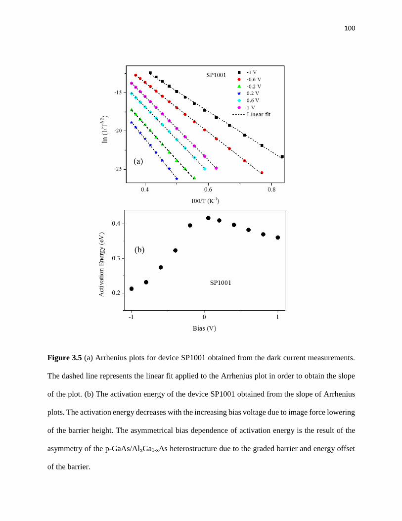
100
Figure 3.5 (a) Arrhenius plots for device SP1001 obtained from the dark current measurements.
The dashed line represents the linear fit applied to the Arrhenius plot in order to obtain the slope
of the plot. (b) The activation energy of the device SP1001 obtained from the slope of Arrhenius
plots. The activation energy decreases with the increasing bias voltage due to image force lowering
of the barrier height. The asymmetrical bias dependence of activation energy is the result of the
asymmetry of the p-GaAs/AlxGa1-xAs heterostructure due to the graded barrier and energy offset
of the barrier.
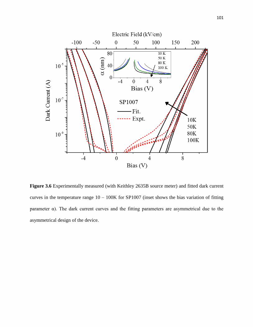
101
Figure 3.6 Experimentally measured (with Keithley 2635B source meter) and fitted dark current
curves in the temperature range 10 – 100K for SP1007 (inset shows the bias variation of fitting
parameter α). The dark current curves and the fitting parameters are asymmetrical due to the
asymmetrical design of the device.
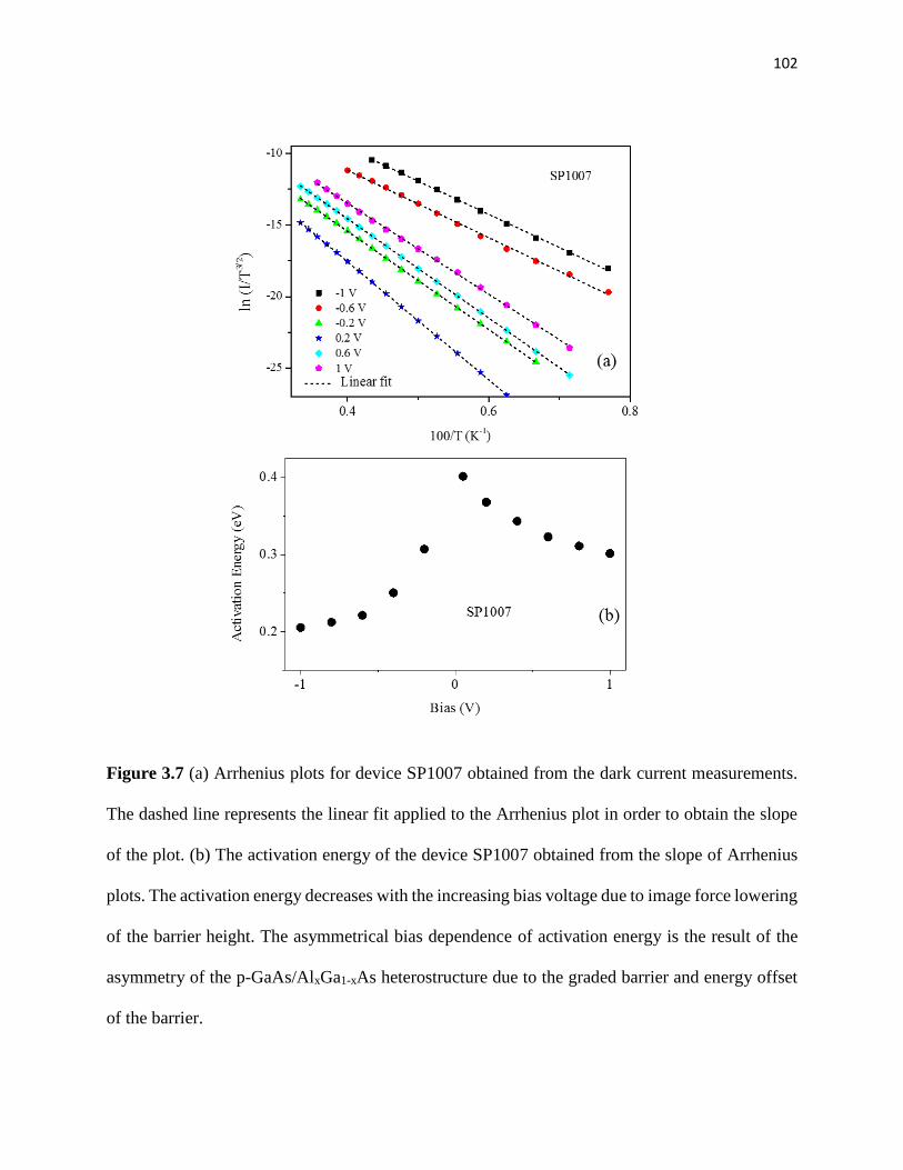
102
Figure 3.7 (a) Arrhenius plots for device SP1007 obtained from the dark current measurements.
The dashed line represents the linear fit applied to the Arrhenius plot in order to obtain the slope
of the plot. (b) The activation energy of the device SP1007 obtained from the slope of Arrhenius
plots. The activation energy decreases with the increasing bias voltage due to image force lowering
of the barrier height. The asymmetrical bias dependence of activation energy is the result of the
asymmetry of the p-GaAs/AlxGa1-xAs heterostructure due to the graded barrier and energy offset
of the barrier.

103
Figure 3.8 Experimentally (with Keithley 2400 source meter) measured and fitted dark current
curves in the temperature range 10 – 100K for GSU17I (inset shows the bias variation of fitting
parameter α). The dark current curves and the fitting parameters are asymmetrical due to the
asymmetrical design of the device.
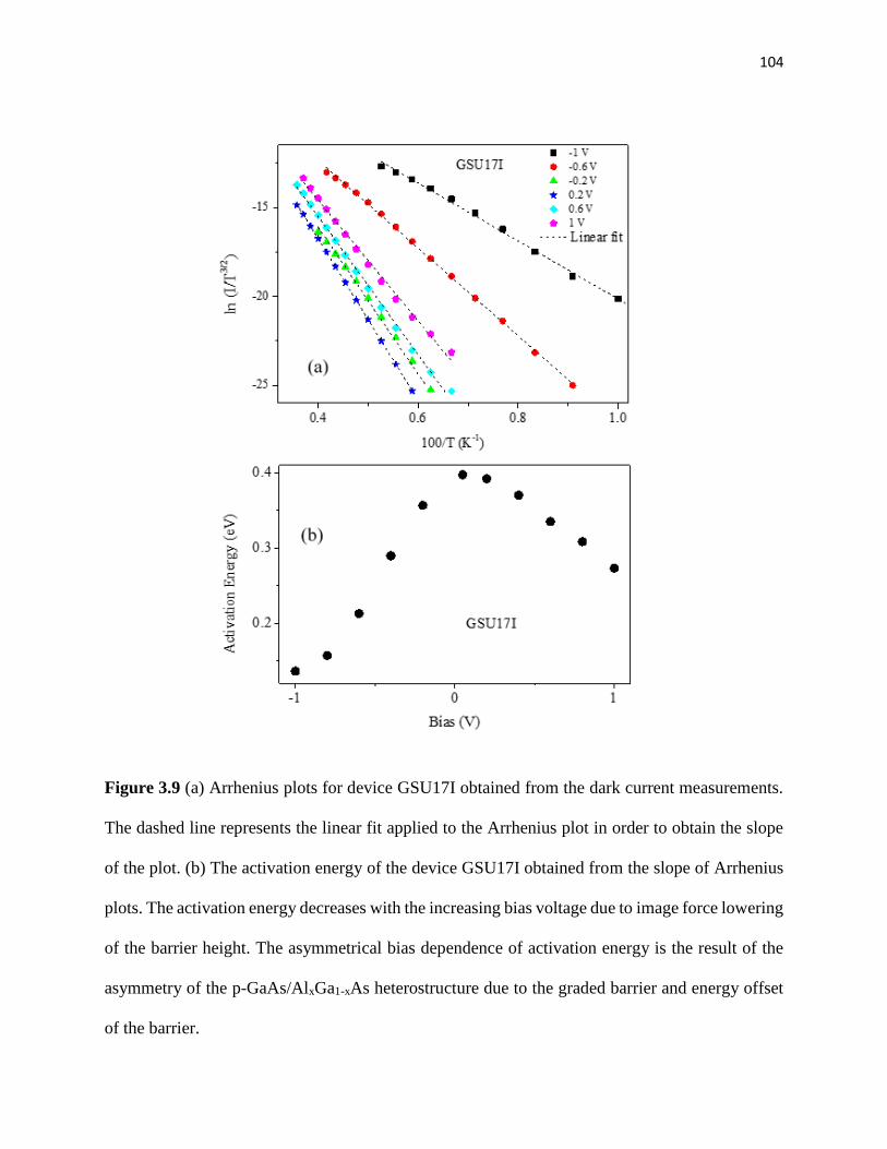
104
Figure 3.9 (a) Arrhenius plots for device GSU17I obtained from the dark current measurements.
The dashed line represents the linear fit applied to the Arrhenius plot in order to obtain the slope
of the plot. (b) The activation energy of the device GSU17I obtained from the slope of Arrhenius
plots. The activation energy decreases with the increasing bias voltage due to image force lowering
of the barrier height. The asymmetrical bias dependence of activation energy is the result of the
asymmetry of the p-GaAs/AlxGa1-xAs heterostructure due to the graded barrier and energy offset
of the barrier.
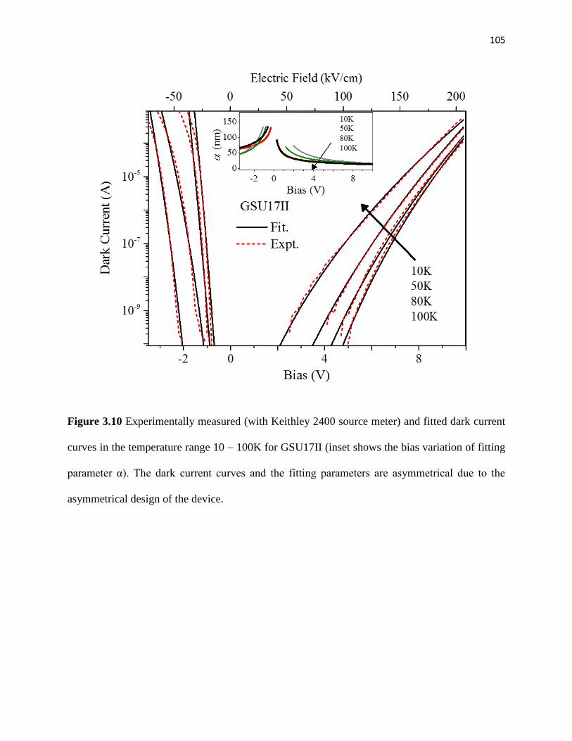
105
Figure 3.10 Experimentally measured (with Keithley 2400 source meter) and fitted dark current
curves in the temperature range 10 – 100K for GSU17II (inset shows the bias variation of fitting
parameter α). The dark current curves and the fitting parameters are asymmetrical due to the
asymmetrical design of the device.
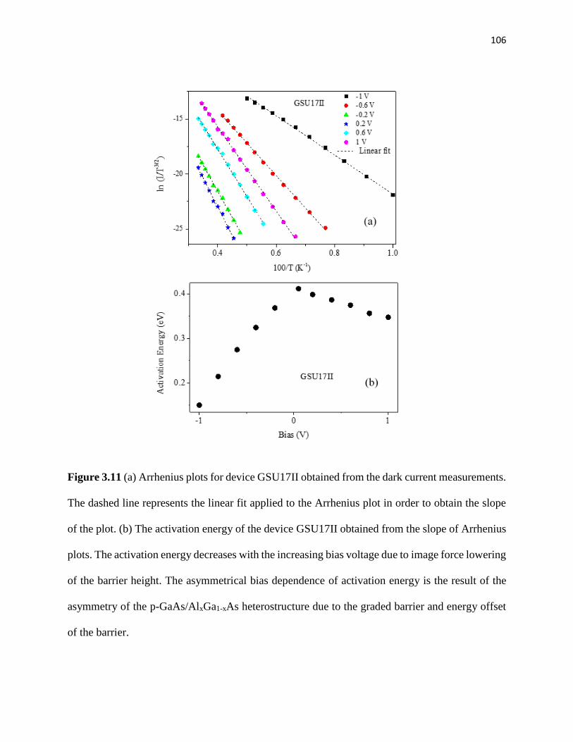
106
Figure 3.11 (a) Arrhenius plots for device GSU17II obtained from the dark current measurements.
The dashed line represents the linear fit applied to the Arrhenius plot in order to obtain the slope
of the plot. (b) The activation energy of the device GSU17II obtained from the slope of Arrhenius
plots. The activation energy decreases with the increasing bias voltage due to image force lowering
of the barrier height. The asymmetrical bias dependence of activation energy is the result of the
asymmetry of the p-GaAs/AlxGa1-xAs heterostructure due to the graded barrier and energy offset
of the barrier.

107
Figure 3.12 Experimentally measured (with Keithley 2400 source meter) and fitted dark current
curves in the temperature range 10 – 100K for GSU17III (inset shows the bias variation of fitting
parameter α). The dark current curves and the fitting parameters are asymmetrical due to the
asymmetrical design of the device.
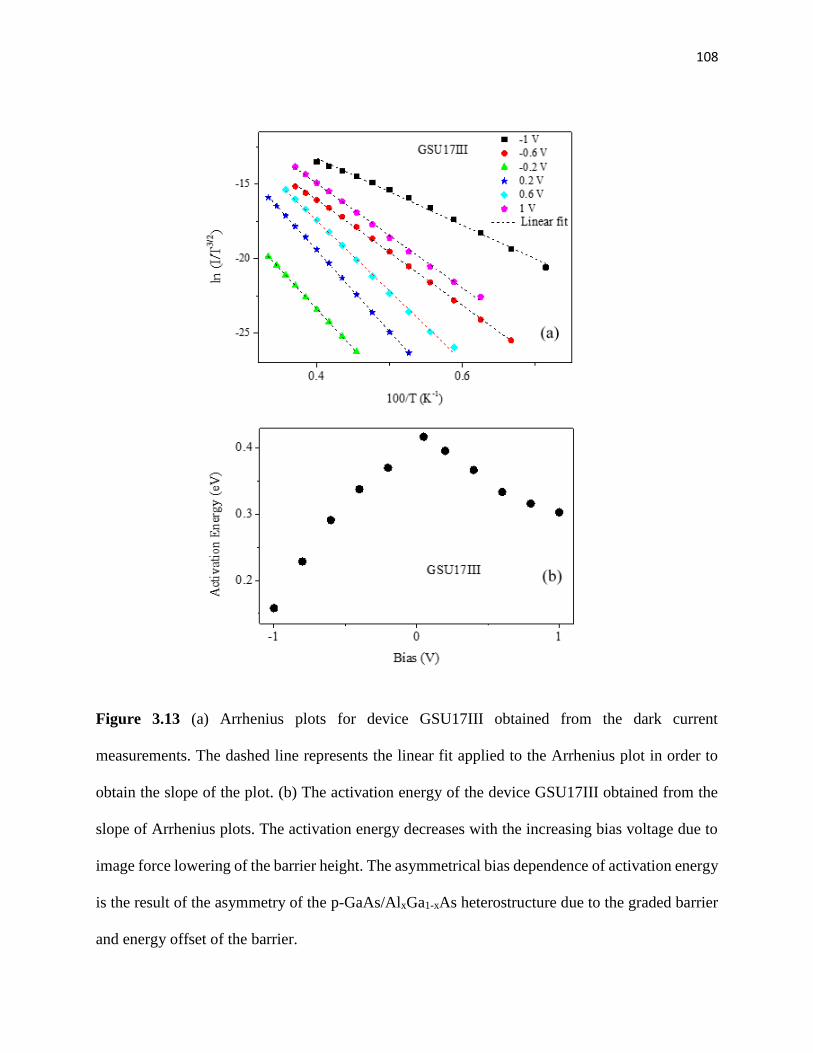
108
Figure 3.13 (a) Arrhenius plots for device GSU17III obtained from the dark current
measurements. The dashed line represents the linear fit applied to the Arrhenius plot in order to
obtain the slope of the plot. (b) The activation energy of the device GSU17III obtained from the
slope of Arrhenius plots. The activation energy decreases with the increasing bias voltage due to
image force lowering of the barrier height. The asymmetrical bias dependence of activation energy
is the result of the asymmetry of the p-GaAs/AlxGa1-xAs heterostructure due to the graded barrier
and energy offset of the barrier.

109
3.3 Summary
The study of the dark current characteristics of the p-GaAs/AlxGa1-xAs heterostructure-
based IR photodetectors confirmed that the dark current is not compromised due to the presence
of the extended-wavelength mechanism of photoresponse. Both in a reference device (LH1002)
and an extended-wavelength IR photodetector, the experimentally measured dark current closely
agreed with the dark current fittings obtained by using a 3D carrier drift model. These results
supported the fact that the extended-wavelength mechanism of IR photoresponse is an exclusively
IR radiation induced phenomenon, and hence the physical properties under dark are not affected
by this phenomenon. These findings are important for further development of IR detectors based
on the extended-wavelength mechanism. These results could be beneficial in developing different
types of optoelectronic devices in the future.
110
4 P-TYPE GAAS/ALGAAS MID-INFRARED PHOTODETECTOR WITH A
CURRENT BLOCKING BARRIER
4.1 Introduction
In a number of recent publications, a significant interest has seen in the area of IR
photodetectors incorporating current blocking structures into detector architectures into detector
designs.86-100 For example, AlGaAs current blocking layers have been utilized in QDIPs in order
to enhance performance,88-93 and also achieve elevated operating temperatures.94-96 Similarly, in
type II InAs/GaSb superlattice (T2SL) IR photodetectors, majority carrier (hole) blocking layers
were implemented.97 In complementary barrier infrared detectors (CBIRD)98 and p-type-intrinsic-
n-type (PbIbN) photodiodes99, electron blocking96 and hole blocking97 unipolar barriers were
incorporated. Furthermore, dark current suppressing structures were demonstrated, such as
conduction band barriers in nBn photodetectors100,101 and XBn barrier photodetectors.102 In
general, the important goal in these device architectures is to lower the dark current, but with a
relatively small compromise to the photoresponse, enabling a significant improvement in the
specific detectivity (D*).
In addition to the mature growth and established processing technology for p-GaAs/
AlxGa1-xAs materials systems, S-O band and L-H/H-H IVB transitions in the p-GaAs spanning the
MIR spectral regime makes this material system attractive for the MIR photo-detection. Moreover,
by including a graded AlxGa1-xAs barrier, the IR photodetector is capable of operation in
photovoltaic mode (i.e., at 0 V) as discussed in Chapter 2.4.2. The photovoltaic operation is
significantly advantageous over photoconductive operation due to its thermal noise limited
performance and reduced power consumption. Additionally, a current blocking barrier (CBB)
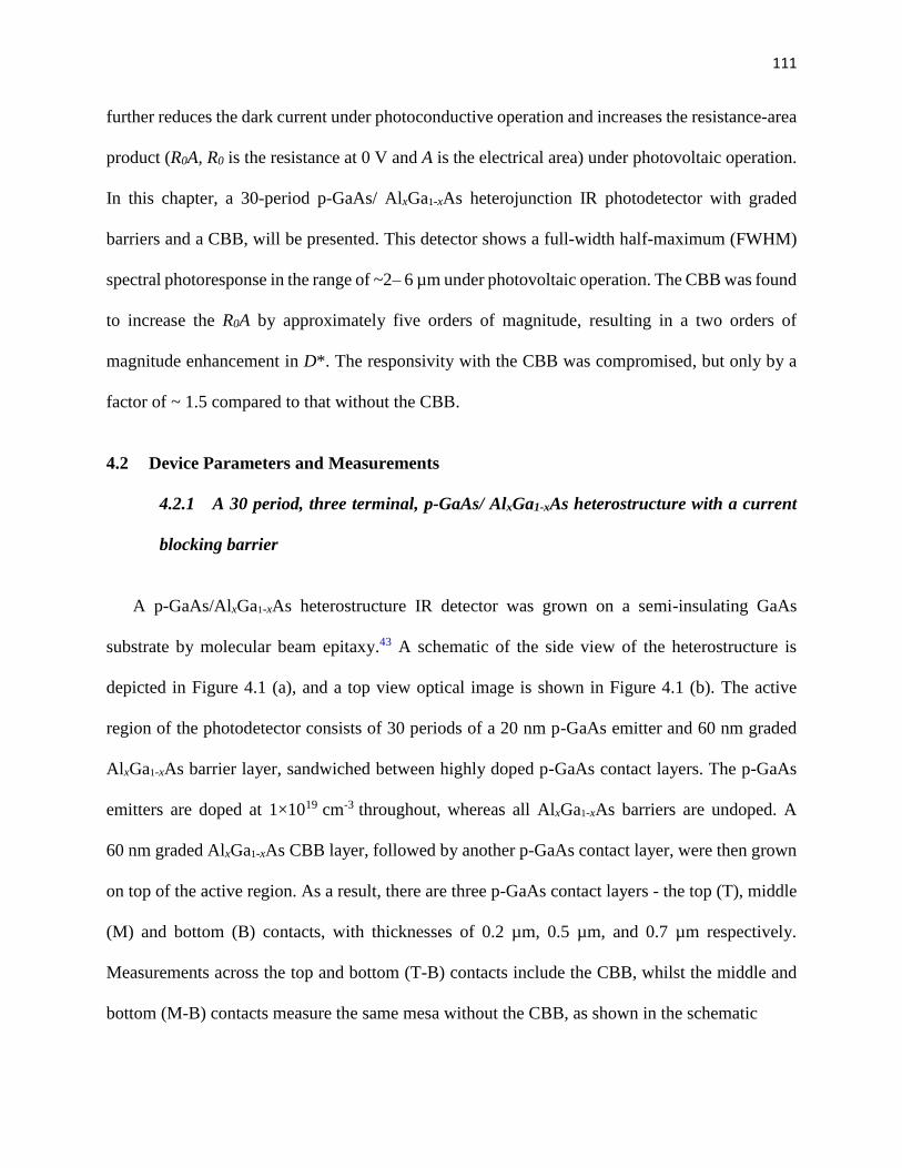
111
further reduces the dark current under photoconductive operation and increases the resistance-area
product (R0A, R0 is the resistance at 0 V and A is the electrical area) under photovoltaic operation.
In this chapter, a 30-period p-GaAs/ AlxGa1-xAs heterojunction IR photodetector with graded
barriers and a CBB, will be presented. This detector shows a full-width half-maximum (FWHM)
spectral photoresponse in the range of ~2– 6 µm under photovoltaic operation. The CBB was found
to increase the R0A by approximately five orders of magnitude, resulting in a two orders of
magnitude enhancement in D*. The responsivity with the CBB was compromised, but only by a
factor of ~ 1.5 compared to that without the CBB.
4.2 Device Parameters and Measurements
4.2.1 A 30 period, three terminal, p-GaAs/ AlxGa1-xAs heterostructure with a current
blocking barrier
A p-GaAs/AlxGa1-xAs heterostructure IR detector was grown on a semi-insulating GaAs
substrate by molecular beam epitaxy.43 A schematic of the side view of the heterostructure is
depicted in Figure 4.1 (a), and a top view optical image is shown in Figure 4.1 (b). The active
region of the photodetector consists of 30 periods of a 20 nm p-GaAs emitter and 60 nm graded
AlxGa1-xAs barrier layer, sandwiched between highly doped p-GaAs contact layers. The p-GaAs
emitters are doped at 1×1019 cm-3 throughout, whereas all AlxGa1-xAs barriers are undoped. A
60 nm graded AlxGa1-xAs CBB layer, followed by another p-GaAs contact layer, were then grown
on top of the active region. As a result, there are three p-GaAs contact layers - the top (T), middle
(M) and bottom (B) contacts, with thicknesses of 0.2 µm, 0.5 µm, and 0.7 µm respectively.
Measurements across the top and bottom (T-B) contacts include the CBB, whilst the middle and
bottom (M-B) contacts measure the same mesa without the CBB, as shown in the schematic
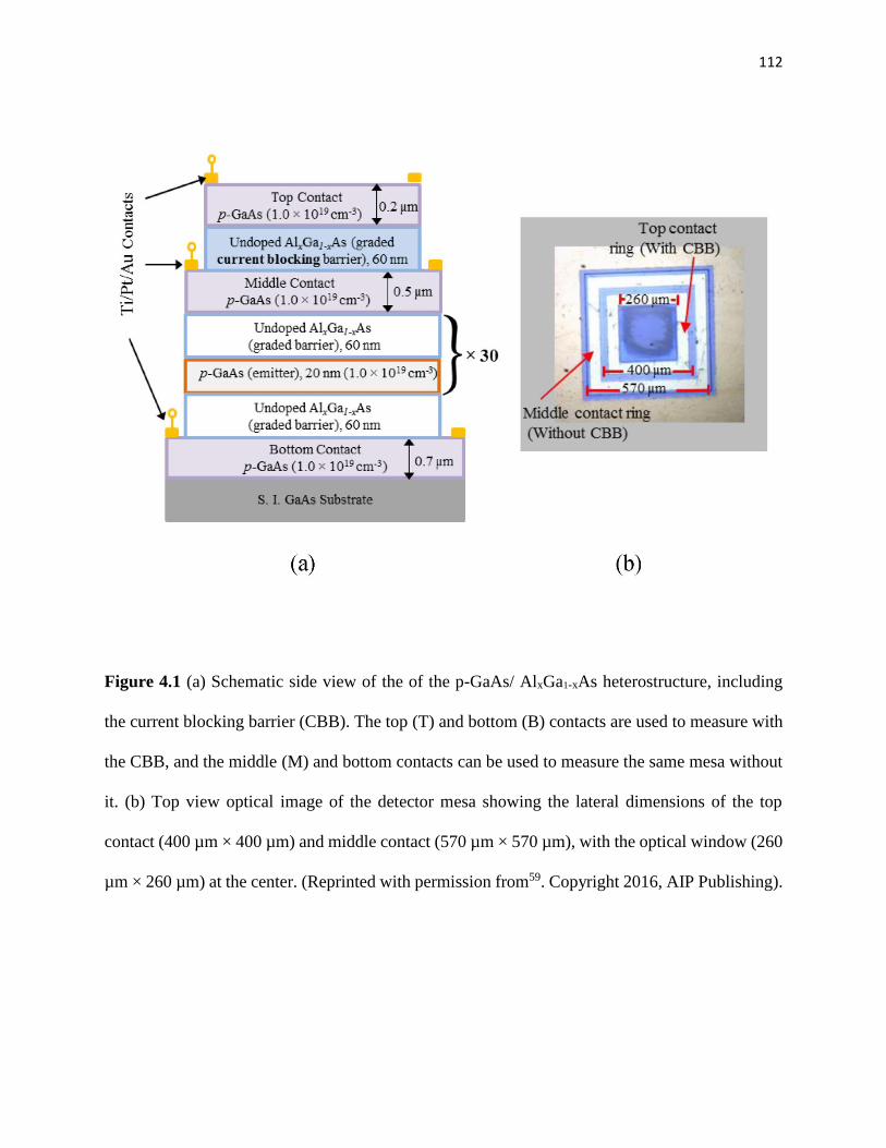
112
Figure 4.1 (a) Schematic side view of the of the p-GaAs/ AlxGa1-xAs heterostructure, including
the current blocking barrier (CBB). The top (T) and bottom (B) contacts are used to measure with
the CBB, and the middle (M) and bottom contacts can be used to measure the same mesa without
it. (b) Top view optical image of the detector mesa showing the lateral dimensions of the top
contact (400 µm × 400 µm) and middle contact (570 µm × 570 µm), with the optical window (260
µm × 260 µm) at the center. (Reprinted with permission from59. Copyright 2016, AIP Publishing).
113
Figure 4.2 (a) Schematic of the valence band alignment of the heterostructure under equilibrium
showing the connections with the CBB and without the CBB. The AlxGa1-xAs barriers are graded
by tuning the Al mole fraction, x. (b) A schematic of the valence band of the GaAs near k = 0,
showing some of the possible hole transitions from light hole/heavy hole to split-off bands, and
also from the heavy hole to light hole band. The emitters are thick enough for bulk-like distribution
of the density of states of carriers. (Reprinted with permission from59. Copyright 2016, AIP
Publishing).
114
diagram of the valence band of the heterostructure in Figure 4.2 (a) Therefore, exactly the same
mesa can be studied with the CBB, and without it. The mesas were processed by a combination of
conventional photolithography, wet etching, and lift-off. The Ti/Pt/Au metal evaporation formed
the metallic contacts on the top, middle, and bottom contact layers. The top and middle mesa
contacts have areas of 400 µm × 400 µm, and 570 µm × 570 µm, respectively. The top p-GaAs
contact layer was partially etched leaving a ~ 20 nm region, to open an optical window (260 µm ×
260 µm, Figure 4.1 (b)) for normal incidence optical illumination. The mesas were wire-bonded
on to a chip carrier for the electrical and optical characterizations.
The AlxGa1-xAs barriers are intentionally graded to create an asymmetry, by tuning x, from
x1 = 0.03 at the bottom to x2 = 0.50 at the top of each barrier. As a result, a potential gradient is
built-up across the barrier. The valence band offsets at the p-GaAs/AlxGa1-xAs interface are ~ 0.017
eV, and ~ 0.28 eV for x = 0.03 and x = 0.50, respectively. This leads to an average potential
gradient of ~ 44 kV/ cm across each AlxGa1-xAs barrier. Similarly, the AlxGa1-xAs CBB was graded
by tuning x, from x1 = 0.53 at the bottom to x2 = 1 at the top, with valence band offsets of ~ 0.29
eV and ~ 0.55 eV, respectively, so that the potential gradient across it is also ~ 44 kV/ cm.
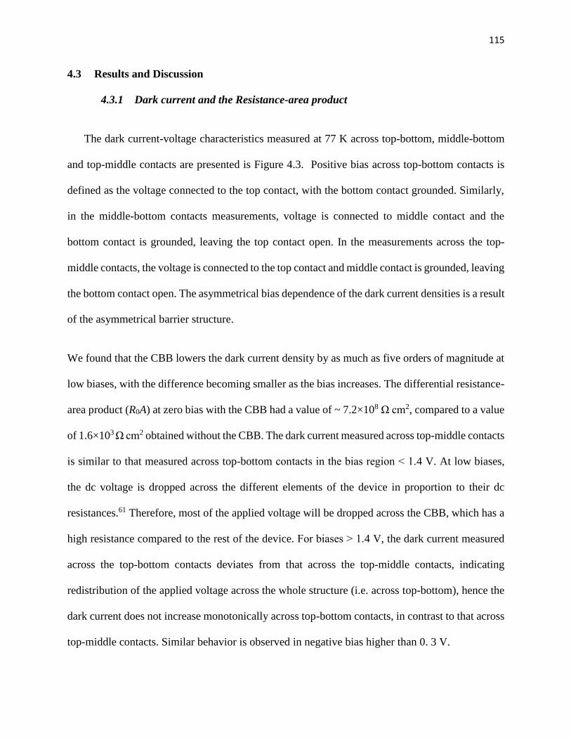
115
4.3 Results and Discussion
4.3.1 Dark current and the Resistance-area product
The dark current-voltage characteristics measured at 77 K across top-bottom, middle-bottom
and top-middle contacts are presented is Figure 4.3. Positive bias across top-bottom contacts is
defined as the voltage connected to the top contact, with the bottom contact grounded. Similarly,
in the middle-bottom contacts measurements, voltage is connected to middle contact and the
bottom contact is grounded, leaving the top contact open. In the measurements across the top-
middle contacts, the voltage is connected to the top contact and middle contact is grounded, leaving
the bottom contact open. The asymmetrical bias dependence of the dark current densities is a result
of the asymmetrical barrier structure.
We found that the CBB lowers the dark current density by as much as five orders of magnitude at
low biases, with the difference becoming smaller as the bias increases. The differential resistance-
area product (R0A) at zero bias with the CBB had a value of ~ 7.2×10⁸ Ω cm2, compared to a value
of 1.6×10³ Ω cm2 obtained without the CBB. The dark current measured across top-middle contacts
is similar to that measured across top-bottom contacts in the bias region ˂ 1.4 V. At low biases,
the dc voltage is dropped across the different elements of the device in proportion to their dc
resistances.61 Therefore, most of the applied voltage will be dropped across the CBB, which has a
high resistance compared to the rest of the device. For biases ˃ 1.4 V, the dark current measured
across the top-bottom contacts deviates from that across the top-middle contacts, indicating
redistribution of the applied voltage across the whole structure (i.e. across top-bottom), hence the
dark current does not increase monotonically across top-bottom contacts, in contrast to that across
top-middle contacts. Similar behavior is observed in negative bias higher than 0. 3 V.
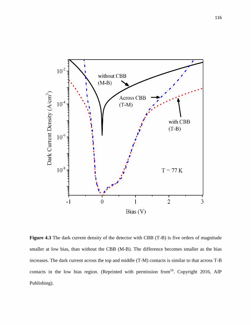
116
Figure 4.3 The dark current density of the detector with CBB (T-B) is five orders of magnitude
smaller at low bias, than without the CBB (M-B). The difference becomes smaller as the bias
increases. The dark current across the top and middle (T-M) contacts is similar to that across T-B
contacts in the low bias region. (Reprinted with permission from59. Copyright 2016, AIP
Publishing).
117
4.3.2 Spectral photoresponse and specific detectivity
The spectral responsivity measured from the same mesa both with and without the CBB,
is shown in Figure 4.4. The 0.34 eV separation of the S-O band from the L-H/H-H band limits the
spectral photoresponse due to the L-H/H-H to S-O bands IVB transitions to ~ 3.6 µm. The spectral
photoresponse beyond 3.6 µm is due to the H-H and L-H band IVB transitions. As a result, two
distinct photoresponse peaks are observed at 2.7 µm and 5.0 µm with responsivities of 0.67 mA/W
and 0.38 mA/W, respectively, in the measurements without the CBB. The FWHM (i.e., 50% cut-
off levels from these peaks) encompasses a ~ 2 – 6 µm spectral range. With inclusion of the CBB,
the measured responsivity of 0.47 mA/W at 2.7 µm is reduced by only a factor of ~ 1.5 from that
obtained without the CBB.
Specific detectivity (D*) under dark condition was obtained using:
kT
ARRD i
0* = (4.1)
where 𝑅𝑖 (A/W) is the spectral responsivity, 𝑘 is the Boltzmann constant, 𝑇 is the temperature,
and A (cm2) is the electrically active area of the detector (400 µm × 400 µm with the CBB, and
570 µm × 570 µm without the CBB). D* was found to be ~ 1.9×10¹¹ Jones at 2.7 µm for the
detector with the CBB, and ~ 4.1×10⁸ Jones without the CBB. A two orders of magnitude higher
D* is therefore obtained with the CBB at zero bias as shown in Figure 4.5. Clearly, the significant
enhancement in the D* is achieved with the high valued of R0A due to the CBB in spite of a small
compromise in the spectral responsivity.
118
Figure 4.4 Comparison of the responsivity of the detector showing that the responsivity with the
CBB is ~ 1.5 times smaller at zero bias, than without the CBB. For the wavelengths ≤ 2 µm, the
energy of photoexcited carriers (≥ 0.6 eV) is much larger than the CBB height (~0.55 eV) and is a
possible reason that the photoresponse is nearly the same in both cases for wavelengths ≤ 2 µm.
(Reprinted with permission from59. Copyright 2016, AIP Publishing).

119
Figure 4.5 Specific detectivity D* showing two orders of magnitude higher detectivity with the
CBB, owing to the higher R0A despite a small reduction in the photoresponse. (Reprinted with
permission from59. Copyright 2016, AIP Publishing).

120
In addition to the measurements at 0 V bias, the photoresponse was measured in the
photoconductive mode as well, with the CBB and without it. The photoresponse increased slightly
with the bias increasing in small steps of 0.2 V as shown in the Figure 4.6 (a) and (b). The bias-
dependence of the peak spectral photoresponse (at 2.7 µm) is shown in Figure 4.7 (a), which
depicts increasing photoresponse with the bias. The effect of applied bias is seen to be more
noticeable at the higher bias region in both cases, that is, with the CBB and without it. The specific
detectivity (D*) under photoconductive operation was obtained by using
AR
kTqJ
RD
diff
i
42
*
+
= (4.2)
where diffR is the differential resistance, q is electronic charge, J is dark current density, and the
other symbols have the same meaning as before. The specific detectivity with and without the CBB
are shown in Figure 4.7 (b). The results show that the specific detectivity (at 2.7 µm) has a
maximum value at 0 V and decreases with the increasing applied bias. This effect is observed to
be stronger at lower biases for the measurements with the CBB. At higher biases, the difference in
the specific detectivity with and without the CBB appears to be small (less than one order of
magnitude). The reason for the decreasing specific detectivity is that the dark current keeps
increasing significantly with increasing bias, whilst the photoresponse increases by a much smaller
magnitude. Therefore, the photovoltaic operation is advantageous over the photoconductive
operation. Since the photovoltaic operation is enabled by the utilization of the graded barriers, they
are also the crucial elements of the heterostructure device architecture.
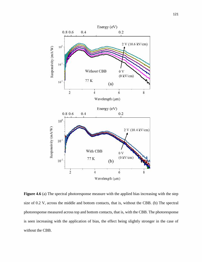
121
Figure 4.6 (a) The spectral photoresponse measure with the applied bias increasing with the step
size of 0.2 V, across the middle and bottom contacts, that is, without the CBB. (b) The spectral
photoresponse measured across top and bottom contacts, that is, with the CBB. The photoresponse
is seen increasing with the application of bias, the effect being slightly stronger in the case of
without the CBB.

122
Figure 4.7 (a) Peak spectral responsivity (at 2.7 µm) from the measurements with the CBB (top-
bottom) and without the CBB (middle-bottom). The applied biases caused a slight increment in
the photoresponse, the effect is more noticeable in the measurement without the CBB. (b) The
specific detectivity (D*) was observed to be maximum at zero bias and it decreased with the
application of bias, thus making the photovoltaic operation more attractive over the
photoconductive operation.
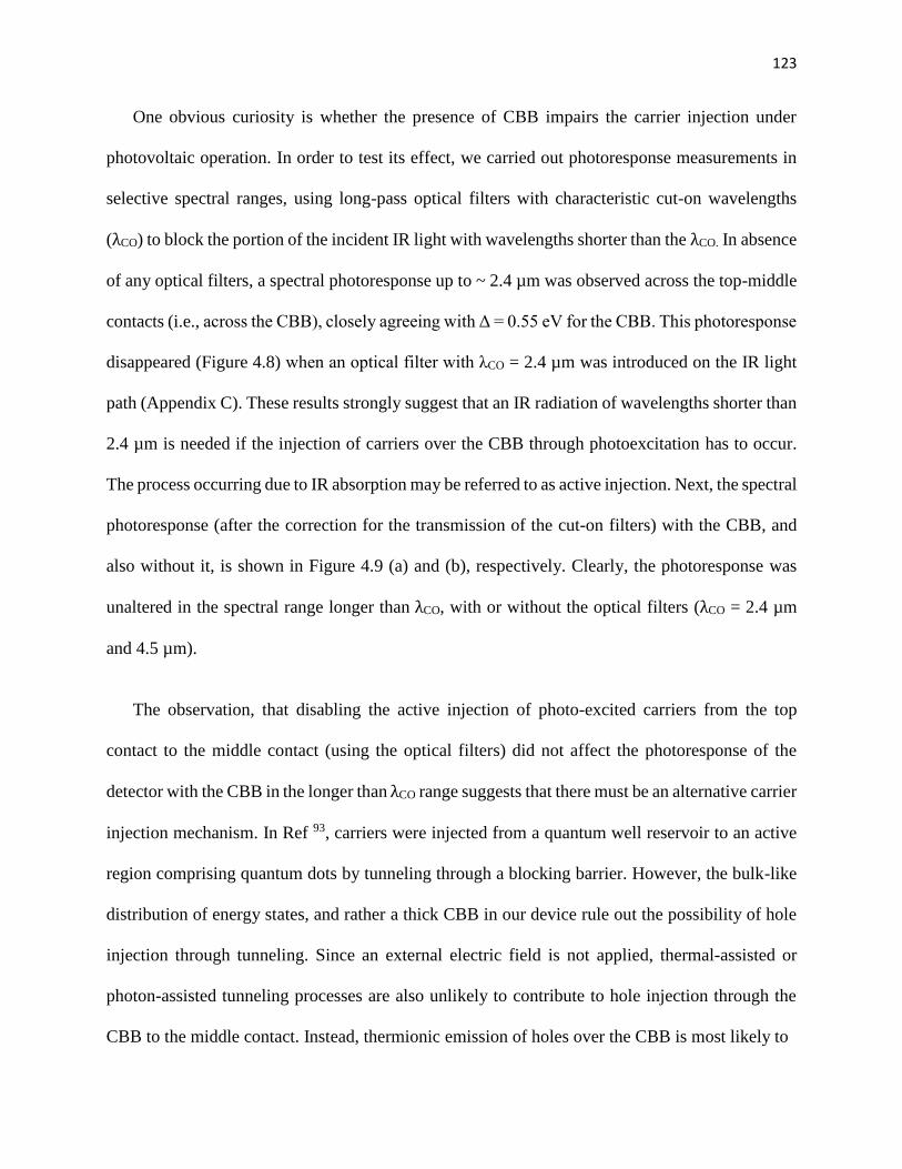
123
One obvious curiosity is whether the presence of CBB impairs the carrier injection under
photovoltaic operation. In order to test its effect, we carried out photoresponse measurements in
selective spectral ranges, using long-pass optical filters with characteristic cut-on wavelengths
(λCO) to block the portion of the incident IR light with wavelengths shorter than the λCO. In absence
of any optical filters, a spectral photoresponse up to ~ 2.4 µm was observed across the top-middle
contacts (i.e., across the CBB), closely agreeing with Δ = 0.55 eV for the CBB. This photoresponse
disappeared (Figure 4.8) when an optical filter with λCO = 2.4 µm was introduced on the IR light
path (Appendix C). These results strongly suggest that an IR radiation of wavelengths shorter than
2.4 µm is needed if the injection of carriers over the CBB through photoexcitation has to occur.
The process occurring due to IR absorption may be referred to as active injection. Next, the spectral
photoresponse (after the correction for the transmission of the cut-on filters) with the CBB, and
also without it, is shown in Figure 4.9 (a) and (b), respectively. Clearly, the photoresponse was
unaltered in the spectral range longer than λCO, with or without the optical filters (λCO = 2.4 µm
and 4.5 µm).
The observation, that disabling the active injection of photo-excited carriers from the top
contact to the middle contact (using the optical filters) did not affect the photoresponse of the
detector with the CBB in the longer than λCO range suggests that there must be an alternative carrier
injection mechanism. In Ref 93, carriers were injected from a quantum well reservoir to an active
region comprising quantum dots by tunneling through a blocking barrier. However, the bulk-like
distribution of energy states, and rather a thick CBB in our device rule out the possibility of hole
injection through tunneling. Since an external electric field is not applied, thermal-assisted or
photon-assisted tunneling processes are also unlikely to contribute to hole injection through the
CBB to the middle contact. Instead, thermionic emission of holes over the CBB is most likely to
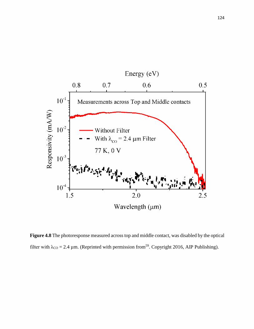
124
Figure 4.8 The photoresponse measured across top and middle contact, was disabled by the optical
filter with λCO = 2.4 µm. (Reprinted with permission from59. Copyright 2016, AIP Publishing).
125
Figure 4.9 Optical filters of cut-on wavelengths of λCO = 2.4 µm and 4.5 µm did not show any
effect on the photoresponse in the spectral range longer than λCO, in the measurements – (a) with
the CBB, and (b) without the CBB.
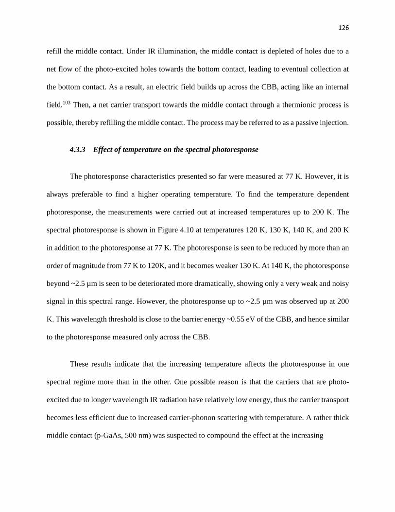
126
refill the middle contact. Under IR illumination, the middle contact is depleted of holes due to a
net flow of the photo-excited holes towards the bottom contact, leading to eventual collection at
the bottom contact. As a result, an electric field builds up across the CBB, acting like an internal
field.103 Then, a net carrier transport towards the middle contact through a thermionic process is
possible, thereby refilling the middle contact. The process may be referred to as a passive injection.
4.3.3 Effect of temperature on the spectral photoresponse
The photoresponse characteristics presented so far were measured at 77 K. However, it is
always preferable to find a higher operating temperature. To find the temperature dependent
photoresponse, the measurements were carried out at increased temperatures up to 200 K. The
spectral photoresponse is shown in Figure 4.10 at temperatures 120 K, 130 K, 140 K, and 200 K
in addition to the photoresponse at 77 K. The photoresponse is seen to be reduced by more than an
order of magnitude from 77 K to 120K, and it becomes weaker 130 K. At 140 K, the photoresponse
beyond ~2.5 µm is seen to be deteriorated more dramatically, showing only a very weak and noisy
signal in this spectral range. However, the photoresponse up to ~2.5 µm was observed up at 200
K. This wavelength threshold is close to the barrier energy ~0.55 eV of the CBB, and hence similar
to the photoresponse measured only across the CBB.
These results indicate that the increasing temperature affects the photoresponse in one
spectral regime more than in the other. One possible reason is that the carriers that are photo-
excited due to longer wavelength IR radiation have relatively low energy, thus the carrier transport
becomes less efficient due to increased carrier-phonon scattering with temperature. A rather thick
middle contact (p-GaAs, 500 nm) was suspected to compound the effect at the increasing
127
Figure 4.10 The spectral photoresponse at temperatures 77K, 120 K, 130 K, 140 K, and 200 K.
The photoresponse is seen to be reduced by an order of magnitude from 77 K to 120 K and becomes
more at 130 K. At 140 K, the photoresponse beyond ~2.5 µm is seen to be deteriorated more
dramatically, showing only a very weak and noisy signal in this spectral range. The spectral
photoresponse up to ~2.5 µm was observed at 200 K.
128
temperatures. In order to test the effect of this thick middle contact, another device with a reduced
thickness was designed and tested, which will be described in the following section.
4.3.4 A single-period, two-terminal p-GaAs/ AlxGa1-xAs heterostructure with a current
blocking barrier (Modified CBB device)
In the previous study, the three-terminal device was used to test the effect of the CBB on
the performance on the same mesa, with and without the CBB. Since the effect has been
demonstrated as seen from the results presented in the previous sections, the new device was
designed to carry out the measurements only across the top and bottom contacts. Therefore, the
middle contact was replaced by a 20 nm p-GaAs as a buffer layer. A schematic of valence band
diagram of the modified CBB device is shown in in Figure 4.11 (a), and Figure 4.11 (b) shows the
dark current density of the device. As shown in Figure 4.11 (a), a single-period emitter-barrier
active region was used instead of the 30-periods used in the previous CBB device. The CBB
parameters were unchanged, whilst the average Al mole fraction in the lower AlxGa1-xAs graded
barrier was slightly higher, from x1 = 0.12 at the bottom to x2 = 0.53 to achieve a slightly shorter
wavelength threshold. Due to this modification, together with the removal of the 500 nm thick
middle contact, the modified CBB device was expected to show an improved spectral
photoresponse at higher operating temperatures.
The spectral photoresponse measured at the temperatures increasing from 77 K to 200 K,
are shown in Figure 4.12 (a) and (b). Unlike the significant reduction in the photoresponse from
77 K to 120 K observed in the previous CBB device (Figure 4.10), the modified CBB device did
not show a reduction in the photoresponse signal from 77 K to 120 K. Instead, the photoresponse

129
Figure 4.11 (a) Schematic of the valence band alignment of modified CBB device under
equilibrium. In comparison to the Figure 4.2 (a), the 500 nm thick middle contact layer is replaced
by a 20 nm buffer layer in the modified CBB device. The Al mole fraction of the graded barrier is
slightly higher, graded from x = 0.12 to 0.53. A single-period emitter/barrier is used instead of
30-periods, thus an average applied electric field corresponding to a particular bias voltage will be
~30 times higher in the modified CBB device compared to the previous CBB device. Due to the
absence of middle contact, the measurements are carried out across the top-bottom contacts only,
that is, with the CBB. (b) Dark current density of the modified CBB device.
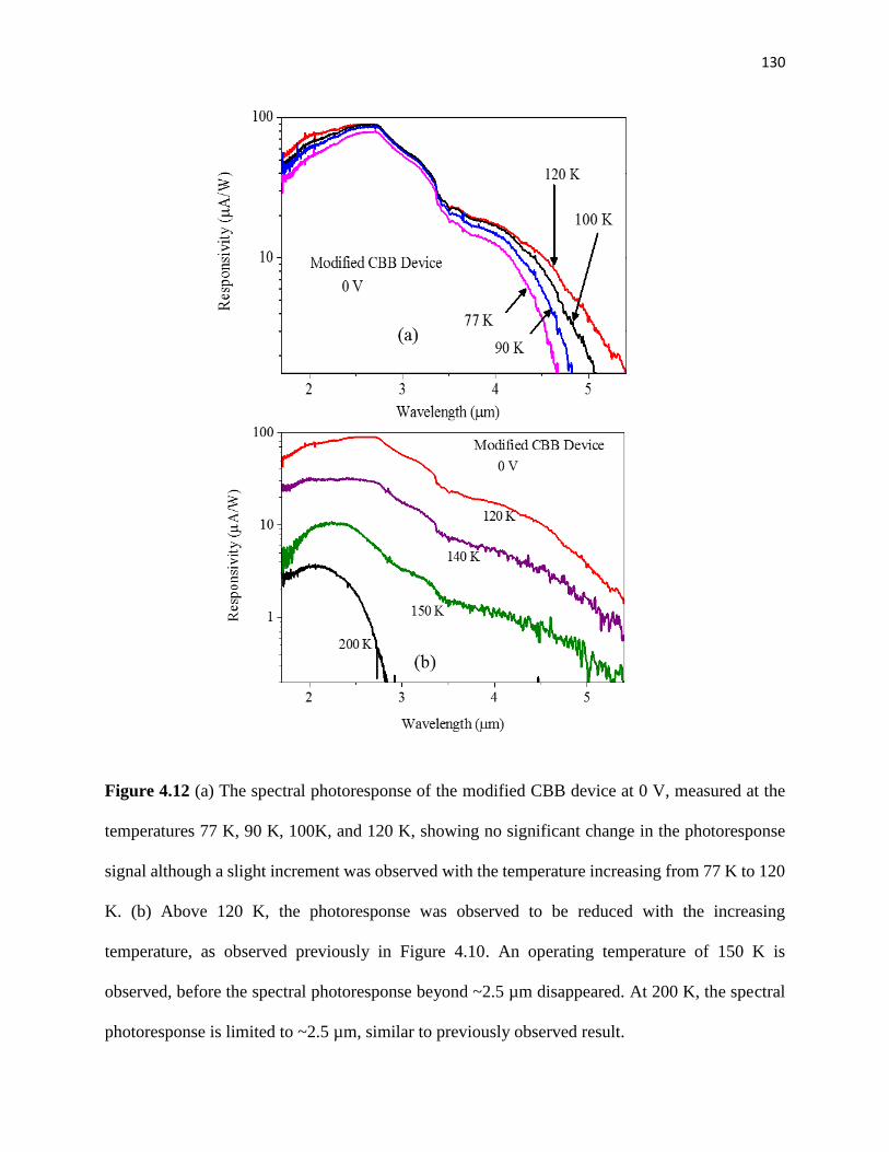
130
Figure 4.12 (a) The spectral photoresponse of the modified CBB device at 0 V, measured at the
temperatures 77 K, 90 K, 100K, and 120 K, showing no significant change in the photoresponse
signal although a slight increment was observed with the temperature increasing from 77 K to 120
K. (b) Above 120 K, the photoresponse was observed to be reduced with the increasing
temperature, as observed previously in Figure 4.10. An operating temperature of 150 K is
observed, before the spectral photoresponse beyond ~2.5 µm disappeared. At 200 K, the spectral
photoresponse is limited to ~2.5 µm, similar to previously observed result.
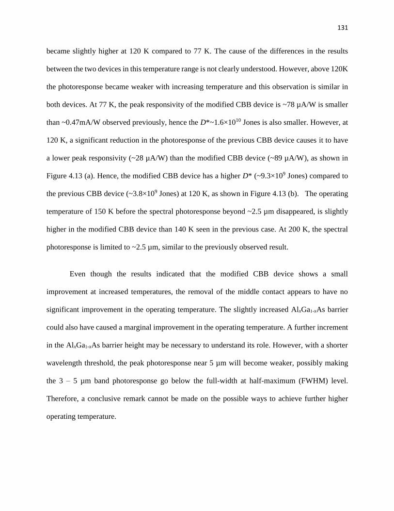
131
became slightly higher at 120 K compared to 77 K. The cause of the differences in the results
between the two devices in this temperature range is not clearly understood. However, above 120K
the photoresponse became weaker with increasing temperature and this observation is similar in
both devices. At 77 K, the peak responsivity of the modified CBB device is ~78 µA/W is smaller
than ~0.47mA/W observed previously, hence the D*~1.6×10¹⁰ Jones is also smaller. However, at
120 K, a significant reduction in the photoresponse of the previous CBB device causes it to have
a lower peak responsivity (~28 µA/W) than the modified CBB device (~89 µA/W), as shown in
Figure 4.13 (a). Hence, the modified CBB device has a higher D* (~9.3×10⁹ Jones) compared to
the previous CBB device (~3.8×10⁹ Jones) at 120 K, as shown in Figure 4.13 (b). The operating
temperature of 150 K before the spectral photoresponse beyond ~2.5 µm disappeared, is slightly
higher in the modified CBB device than 140 K seen in the previous case. At 200 K, the spectral
photoresponse is limited to ~2.5 µm, similar to the previously observed result.
Even though the results indicated that the modified CBB device shows a small
improvement at increased temperatures, the removal of the middle contact appears to have no
significant improvement in the operating temperature. The slightly increased AlxGa1-xAs barrier
could also have caused a marginal improvement in the operating temperature. A further increment
in the AlxGa1-xAs barrier height may be necessary to understand its role. However, with a shorter
wavelength threshold, the peak photoresponse near 5 µm will become weaker, possibly making
the 3 – 5 µm band photoresponse go below the full-width at half-maximum (FWHM) level.
Therefore, a conclusive remark cannot be made on the possible ways to achieve further higher
operating temperature.
132
Figure 4.13 A comparison between the CBB device and the modified CBB device in terms of (a)
spectral photoresponse, and (b) specific detectivity (D*) at 120 K, 0 V. The modified CBB device
is seen to have a higher responsivity and the specific detectivity.
133
4.4 Future work on MIR (3 – 5 µm) photodetectors based on p-type InP and GaInPAs
based III-V semiconductor materials
The S-O band energy (ΔS-O = 0.34 eV) of the GaAs limits the spectral photoresponse to
~3.6 µm, with the peak response being near 2.7 µm. The H-H/L-H transitions give rise to the
photoresponse with a peak near 5 µm or beyond. In between the two peaks, the photoresponse is
weak, in the 3 – 5 µm regime, which is the most important band being an atmospheric window.
Other materials with the S-O band energy in the IR regime are InAs (ΔS-O = 0.41 eV), AlAs
(ΔS-O = 0.30 eV), InP (ΔS-O = 0.11 eV), GaP (ΔS-O = 0.08 eV), and AlP (ΔS-O = 0.07 eV). InAs and
AlAs are not much different from GaAs for the 3 – 5 µm band. However, InP with the S-O energy
of 0.11 eV can cover the spectral absorption up to ~11 µm. In fact, the experimentally measured
absorption104 of p-type InP show a uniform absorption in a broad spectral range, including the 3 –
5 µm. Therefore, p-type InP based heterostructures are proposed for the 3 – 5 µm band IR
detection.
A design of the p-InP/InAlAs heterostructure based IR photodetector is depicted in Figure
4.14. Three heterostructures (GS-LWIR-1, GS-LWIR-2, and GS-LWIR-3) are under production
at the time of this writing. These structures are grown by MBE on InP substrate. The active region
of the device consists of p-type doped (with Be dopant) InP emitter between undoped In0.52Al0.48As
(60 nm) barriers. This region is sandwiched between the top and bottom contacts. The top contact
consists of p-type, highly doped (>1.0×1019 cm-3) p-In0.53Ga0.47As (50 nm) and p-type InP (20 nm).
The bottom contact consists of highly doped (>1.0×1019 cm-3) p-In0.53Ga0.47As (400 nm). The p-
InP emitter in the device GS-LWIR-1 is 20 nm, with 3.0×1018 cm-3 doping. But in the device GS-
LWIR-2, the p-InP emitter is 80 nm, with 3.0×1018 cm-3 doping. In the GS-LWIR-3, the p-InP
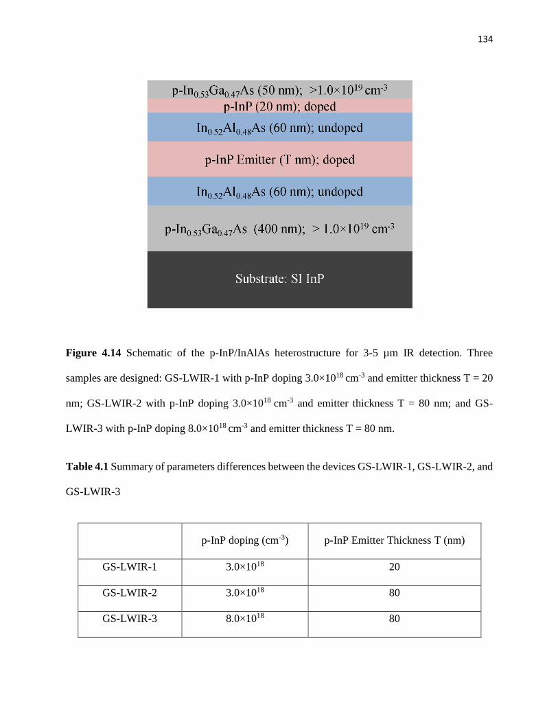
134
Figure 4.14 Schematic of the p-InP/InAlAs heterostructure for 3-5 µm IR detection. Three
samples are designed: GS-LWIR-1 with p-InP doping 3.0×1018 cm-3 and emitter thickness T = 20
nm; GS-LWIR-2 with p-InP doping 3.0×1018 cm-3 and emitter thickness T = 80 nm; and GS-
LWIR-3 with p-InP doping 8.0×1018 cm-3 and emitter thickness T = 80 nm.
Table 4.1 Summary of parameters differences between the devices GS-LWIR-1, GS-LWIR-2, and
GS-LWIR-3
p-InP doping (cm-3) p-InP Emitter Thickness T (nm)
GS-LWIR-1 3.0×10¹⁸ 20
GS-LWIR-2 3.0×10¹⁸ 80
GS-LWIR-3 8.0×10¹⁸ 80
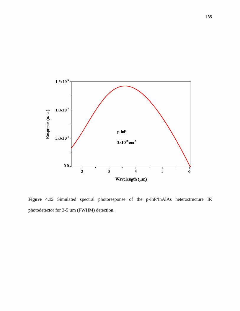
135
Figure 4.15 Simulated spectral photoresponse of the p-InP/InAlAs heterostructure IR
photodetector for 3-5 µm (FWHM) detection.

136
emitter is 80 nm, with a higher doping at 8.0×1018 cm-3. The differences in the parameters in the
three devices are summarized in Table 4.1.
The spectral photoresponse is simulated by using the absorption coefficient data104 for
3.0×1018 cm-3 doping of p-InP is shown in Figure 4.15. The FWHM of photoresponse is observed
in the 3 – 5 µm band. The simulation is based on escape cone model41 of internal photoemission.
It is encouraging to see the photoresponse peak is in the 3 – 5 µm band, and the devices are
expected show their spectral photoresponse similar to the simulated result.
Once the experimental results of these devices are studied, further modifications in the
designs are possible to include graded barrier by gradually increasing the Al mole fraction in the
In0.52Al0.48As barrier. The graded barrier will enable photovoltaic operation and enhance the D*
due to thermal noise limited operation. A current-blocking barrier may also be used to further
enhance the D*.
Another alternative of IR absorber with S-O band transition is the quaternary III-V material
GaxIn1-xAsyP1-y with the ΔS-O(y) varying from 0.38 eV to 0.11 eV as (0.11+0.421y-0.152y²) with
the As composition.82 The As composition with y = 0.36 will give a ΔS-O (0.36) ~0.24 eV, which
yields a wavelength close to 5 µm. This composition may be useful to achieve a S-O band
absorption peak in the 3 – 5 µm band. Furthermore, undoped AlxGa1-xAs layers can be used as
barriers, with a flexibility in terms of Al mole fraction variation for graded barriers, except for
some lattice-matching restriction at the beginning of the layer growth.
137
4.5 Summary
A 2 – 6 µm IR photodetector, based on p-GaAs/AlxGa1-xAs heterostructure, operating at 0
V, was found to benefit from a current blocking barrier. S-O band and H-H/L-H band IVB
transitions due to IR absorption enabled the photodetection. The specific detectivity was increased
by two orders of magnitude, to ~1.9×10¹¹ Jones, due to the current blocking barrier although a
small compromise in the spectral responsivity (by a factor of ~1.5) was observed. Selective spectral
measurements, by using long-pass optical filters, confirmed that the spectral photoresponse carrier
injection is not affected by the current blocking barrier. Furthermore, a 3 – 5 µm band IR
photodetector, currently under development, is discussed as an alternative to p-GaAs absorber,
since the S-O band peak (~2.7 µm) and H-H/L-H peak (~5 µm) cause a slightly weaker
photoresponse in this atmospheric window. A S-O band tuning is possible in another material
system, GaInAsP from ~3.2 µm to ~11 µm. The possibility of using this material system is also
discussed to develop a S-O band IR photodetector for 3 – 5 µm band use.

138
REFERENCES
1 William Herschel, Philosophical Transactions of the Royal Society of London 90, 284
(1800).
2 A. Rogalski, Infrared Detectors, Second Edition. (CRC Press, 2010).
3 Gabby Sarusi, Infrared Physics & Technology 44 (5), 439 (2003).
4 Victor S. Cheng, Jinfen Bai, and Yazhu Chen, Medical Engineering & Physics 31 (9),
1173 (2009).
5 B. B. Lahiri, S. Bagavathiappan, T. Jayakumar, and John Philip, Infrared Physics &
Technology 55 (4), 221 (2012).
6 A. Rogalski, Opto-Electron. Rev. 20 (3), 279 (2012).
7 P. Norton, Opto-Electron. Rev. 14 (1), 1 (2006).
8 Greggory H Rothmeier, Thesis, Georgia State University, 2012.
9 M. Izzetoglu, S. C. Bunce, K. Izzetoglu, B. Onaral, and K. Pourrezaei, IEEE Engineering
in Medicine and Biology Magazine 26 (4), 38 (2007).
10 Kurtulus Izzetoglu, Scott Bunce, Banu Onaral, Kambiz Pourrezaei, and Britton Chance,
International Journal of Human–Computer Interaction 17 (2), 211 (2004).
11 Muhammad A. Kamran, Myung Yung Jeong, and Malik M. N. Mannan, Frontiers in
behavioral neuroscience 9, 151 (2015).
12 Arno Villringer and Britton Chance, Trends Neurosci 20 (10), 435 (1997).
13 Muhammad A. Kamran, Malik M. Naeem Mannan, and Myung Yung Jeong, Frontiers in
Human Neuroscience 10 (261) (2016).
14 Isabel de Roever, Gemma Bale, Subhabrata Mitra, Judith Meek, Nicola J. Robertson, and
Ilias Tachtsidis, Frontiers in human neuroscience 12, 371 (2018).

139
15 Muhammad A. Kamran, Malik M. N. Mannann, and Myung Yung Jeong, Frontiers in
Neuroinformatics 12 (37) (2018).
16 Paola Pinti, Ilias Tachtsidis, Antonia Hamilton, Joy Hirsch, Clarisse Aichelburg, Sam
Gilbert, and Paul W. Burgess, Annals of the New York Academy of Sciences, Special Issue,
1-25, (2018).
17 J. Réhault, R. Borrego-Varillas, A. Oriana, C. Manzoni, C. P. Hauri, J. Helbing, and G.
Cerullo, Opt. Express 25 (4), 4403 (2017).
18 Jitto Titus, Emilie Viennois, Didier Merlin, and A. G. Unil Perera, Journal of Biophotonics
10 (3), 465 (2017).
19 Hemendra Ghimire, Mahathi Venkataramani, Zhen Bian, Yuan Liu, and A. G. Unil Perera,
Scientific Reports 7 (1), 16993 (2017).
20 Jitto Titus, Hemendra Ghimire, Emilie Viennois, Didier Merlin, and A. G. Unil Perera,
Journal of Biophotonics 11 (3), e201700057 (2018).
21 A.L. Smith, The Coblentz Society Desk Book of Infrared Spectra, Second Edition. (The
Coblentz Society, Kirkwood, MO, 1982).
22 A. Rogalski, Infrared Physics & Technology 54 (3), 136 (2011).
23 A. Rogalski, Progress in Quantum Electronics 27 (2–3), 59 (2003).
24 B. F. Levine, Journal of Applied Physics 74 (8), R1 (1993).
25 S. Krishna, S. D. Gunapala, S. V. Bandara, C. Hill, and D. Z. Ting, Proceedings of the
IEEE 95 (9), 1838 (2007).
26 A. G. U. Perera, H. X. Yuan, S. K. Gamage, W. Z. Shen, M. H. Francombe, H. C. Liu, M.
Buchanan, and W. J. Schaff, Journal of Applied Physics 81 (7), 3316 (1997).
140
27 A. G. U. Perera, W. Z. Shen, H. C. Liu, M. Buchanan, and W. J. Schaff, Materials Science
and Engineering: B 74 (1), 56 (2000).
28 W. Songprakob, R. Zallen, D. V. Tsu, and W. K. Liu, J. Appl. Phys. 91 (1), 171 (2002).
29 S. G. Matsik, M. B. M. Rinzan, D. G. Esaev, A. G. U. Perera, H. C. Liu, and M. Buchanan,
Applied Physics Letters 84 (18), 3435 (2004).
30 D. G. Esaev, M. B. M. Rinzan, S. G. Matsik, and A. G. U. Perera, Journal of Applied
Physics 96 (8), 4588 (2004).
31 A. G. U. Perera, S. G. Matsik, P. V. V. Jayaweera, K. Tennakone, H. C. Liu, M. Buchanan,
G. Von Winckel, A. Stintz, and S. Krishna, Applied Physics Letters 89 (13) (2006).
32 P. V. V. Jayaweera, S. G. Matsik, K. Tennakone, A. G. U. Perera, H. C. Liu, and S. Krishna,
Infrared Physics & Technology 50 (2), 279 (2007).
33 P. V. V. Jayaweera, S. G. Matsik, A. G. U. Perera, H. C. Liu, M. Buchanan, and Z. R.
Wasilewski, Appl. Phys. Lett. 93 (2), 021105 (2008).
34 S. G. Matsik, P. V. V. Jayaweera, A. G. U. Perera, K. K. Choi, and P. Wijewarnasuriya, J.
Appl. Phys. 106 (6), 064503 (2009).
35 S. M. Sze and K. K. Ng, Physics of semiconductor devices, 3rd ed. (Wiley-Interscience,
Hoboken, New Jersey, 2007).
36 Yan-Feng Lao, A. G. Unil Perera, L. H. Li, S. P. Khanna, E. H. Linfield, and H. C. Liu,
Nature Photonics 8, 412 (2014).
37 Dilip Chauhan, A. G. Unil Perera, Lianhe Li, Li Chen, Suraj P. Khanna, and Edmund H.
Linfield, Otic. Eng. 56 (9), 091605 (2017).
38 D. Chauhan, A. G. U. Perera, L. H. Li, L. Chen, and E. H. Linfield, Journal of Applied
Physics 122 (2), 024501 (2017).

141
39 Yan-Feng Lao and A. G. Unil Perera, J. Appl. Phys. 109 (10), 103528 (2011).
40 Yan-Feng Lao and A. G. Unil Perera, Physical Review B 86 (19), 195315 (2012).
41 A. G. U. Perera, H. X. Yuan, and M. H. Francombe, Journal of Applied Physics 77 (2),
915 (1995).
42 A. M. Hoang, G. Chen, A. Haddadi, S. Abdollahi Pour, and M. Razeghi, Applied Physics
Letters 100 (21), 211101 (2012).
43 L. H. Li, J. X. Zhu, L. Chen, A. G. Davies, and E. H. Linfield, Opt. Express 23 (3), 2720
(2015).
44 E.R. Weber, R.K. Willardson, H.C. Liu, and F. Capasso, Intersubband Transitions in
Quantum Wells: Physics and Device Applications. (Elsevier Science, 1999).
45 Y. F. Lao, P. K. D. D. P. Pitigala, A. G. U. Perera, H. C. Liu, M. Buchanan, Z. R.
Wasilewski, K. K. Choi, and P. Wijewarnasuriya, Appl. Phys. Lett. 97 (9), 091104 (2010).
46 Y. F. Lao and A. G. U. Perera, Advances in OptoElectronics 2016, 18 (2016).
47 Alvin M. Goodman, Physical Review 152 (2), 785 (1966).
48 V. E. Vickers, Appl. Opt. 10 (9), 2190 (1971).
49 Yan-Feng Lao, A. G. Unil Perera, L. H. Li, S. P. Khanna, E. H. Linfield, Y. H. Zhang, and
T. M. Wang, Opt. Lett. 41 (2), 285 (2016).
50 Mark L. Brongersma, Naomi J. Halas, and Peter Nordlander, Nat Nano 10 (1), 25 (2015).
51 Nathaniel M. Gabor, Justin C. W. Song, Qiong Ma, Nityan L. Nair, Thiti Taychatanapat,
Kenji Watanabe, Takashi Taniguchi, Leonid S. Levitov, and Pablo Jarillo-Herrero,
Science 334 (6056), 648 (2011).
52 Marcus Freitag, Tony Low, Fengnian Xia, and Phaedon Avouris, Nat Photon 7 (1), 53
(2013).

142
53 Yaohui Zhan, Kai Wu, Cheng Zhang, Shaolong Wu, and Xiaofeng Li, Opt. Lett. 40 (18),
4261 (2015).
54 D. Chauhan, A. G. U. Perera, L. Li, L. Chen, and E. H. Linfield, IEEE Sensors Letters 2
(4), 1 (2018).
55 D. Sicault, R. Teissier, F. Pardo, J. L. Pelouard, and F. Mollot, Physical Review B 65 (12),
121301 (2002).
56 V. B. Campos, S. Das Sarma, and M. A. Stroscio, Physical Review B 46 (7), 3849 (1992).
57 V. B. Campos and S. Das Sarma, Physical Review B 45 (7), 3898 (1992).
58 P. V. V. Jayaweera, S. G. Matsik, A. G. U. Perera, H. C. Liu, M. Buchanan, and Z. R.
Wasilewski, Applied Physics Letters 93 (2), 021105 (2008).
59 D. Chauhan, A. G. U. Perera, L. H. Li, L. Chen, and E. H. Linfield, Applied Physics Letters
108 (20), 201105 (2016).
60 P. K. D. D. P. Pitigala, S. G. Matsik, A. G. U. Perera, S. P. Khanna, L. H. Li, E. H. Linfield,
Z. R. Wasilewski, M. Buchanan, and H. C. Liu, J. Appl. Phys. 111 (8), 084505 (2012).
61 H. C. Liu, J. Li, J. R. Thompson, Z. R. Wasilewski, M. Buchanan, and J. G. Simmons,
IEEE Transactions on Electron Devices 40 (11), 2142 (1993).
62 A. G. U. Perera, Dilip Chauhan, Yan-Feng Lao, Lianhe Li, Suraj P. Khanna, and Edmund
H. Linfield, 2016 Proc. SPIE 9844, Automatic Target Recognition XXVI, 98440X (2016).
63 Antonio C. S. Algarte, Physical Review B 38 (3), 2162 (1988).
64 W. Pötz, Physical Review B 36 (9), 5016 (1987).
65 R. P. Joshi and D. K. Ferry, Physical Review B 39 (2), 1180 (1989).
66 T. Inoshita and H. Sakaki, Physica B: Condensed Matter 227 (1), 373 (1996).
67 S. Gupta, S. Sethi, and P. K. Bhattacharya, Applied Physics Letters 62 (10), 1128 (1993).
143
68 Y. Rosenwaks, M. C. Hanna, D. H. Levi, D. M. Szmyd, R. K. Ahrenkiel, and A. J. Nozik,
Physical Review B 48 (19), 14675 (1993).
69 E. A. Zibik, T. Grange, B. A. Carpenter, N. E. Porter, R. Ferreira, G. Bastard, D. Stehr, S.
Winnerl, M. Helm, H. Y. Liu, M. S. Skolnick, and L. R. Wilson, Nat Mater 8 (10), 803
(2009).
70 Yukihiro Harada, Naofumi Kasamatsu, Daiki Watanabe, and Takashi Kita, Physical
Review B 93 (11), 115303 (2016).
71 Y. C. Chang, A. J. Robson, S. Harrison, Q. D. Zhuang, and M. Hayne, AIP Advances 5
(6), 067141 (2015).
72 Ye Yang, David P. Ostrowski, Ryan M. France, Kai Zhu, Jao van de Lagemaat, Joseph M.
Luther, and Matthew C. Beard, Nature Photonics 10, 53 (2015).
73 William A. Tisdale, Kenrick J. Williams, Brooke A. Timp, David J. Norris, Eray S. Aydil,
and X.-Y. Zhu, Science 328 (5985), 1543 (2010).
74 J. S. Blakemore, Journal of Applied Physics 53 (10), R123 (1982).
75 Sanjay Krishna, Infrared Physics & Technology 47 (1), 153 (2005).
76 Seyoum Wolde, Yan-Feng Lao, A. G. Unil Perera, Y. H. Zhang, T. M. Wang, J. O. Kim,
Ted Schuler-Sandy, Zhao-Bing Tian, and S. Krishna, Applied Physics Letters 105 (15),
151107 (2014).
77 Yan-Feng Lao, Seyoum Wolde, A. G. Unil Perera, Y. H. Zhang, T. M. Wang, J. O. Kim,
Ted Schuler-Sandy, Zhao-Bing Tian, and S. S. Krishna, Applied Physics Letters 104 (17),
171113 (2014).
144
78 M.S. Park, V. Jain, E.H. Lee, S.H. Kim, H. Pettersson, Q. Wang, J.D. Song, and W.J. Choi,
in Electronics Letters (Institution of Engineering and Technology, 2014), Vol. 50, pp.
1731.
79 E. A. Zibik, A. M. Adawi, L. R. Wilson, A. Lemaître, J. W. Cockburn, M. Hopkinson, and
G. Hill, Journal of Applied Physics 100 (1), 013106 (2006).
80 Yu Yao, Anthony J. Hoffman, and Claire F. Gmachl, Nature Photonics 6, 432 (2012).
81 Antoine Godard, Comptes Rendus Physique 8 (10), 1100 (2007).
82 M. Levinshtein, S. Rumyantsev, and M. Shur, Handbook Series on Semiconductor
Parameters: Ternary and quaternary A3B5 semiconductors. (World Scientific, 1999).
83 R. Quay, C. Moglestue, V. Palankovski, and S. Selberherr, Materials Science in
Semiconductor Processing 3 (1–2), 149 (2000).
84 M. Z. Tidrow, J. C. Chiang, Sheng S. Li, and K. Bacher, Applied Physics Letters 70 (7),
859 (1997).
85 D. K. Sengupta, S. L. Jackson, D. Ahmari, H. C. Kuo, J. I. Malin, S. Thomas, M. Feng, G.
E. Stillman, Y. C. Chang, L. Li, and H. C. Liu, Applied Physics Letters 69 (21), 3209
(1996).
86 D. K. Sengupta, S. L. Jackson, A. P. Curtis, W. Fang, J. I. Malin, T. U. Horton, Q. Hartman,
H. C. Kuo, S. Thomas, J. Miller, K. C. Hsieh, I. Adesida, S. L. Chuang, M. Feng, G. E.
Stillman, Y. C. Chang, W. Wu, J. Tucker, H. Chen, J. M. Gibson, J. Mazumder, L. Li, and
H. C. Liu, Journal of Elec Materi 26 (12), 1376 (1997).
87 D. K. Sengupta, M. B. Weisman, M. Feng, S. L. Chuang, Y. C. Chang, L. Cooper, I.
Adesida, I. Bloom, K. C. Hsieh, W. Fang, J. I. Malin, A. P. Curtis, T. Horton, G. E.

145
Stillman, S. D. Gunapala, S. V. Bandara, F. Pool, J. K. Liu, M. McKelvey, E. Luong, W.
Hong, J. Mumolo, H. C. Liu, and W. I. Wang, Journal of Elec Materi 27 (7), 858 (1998).
88 S. Y. Wang, S. D. Lin, H. W. Wu, and C. P. Lee, Applied Physics Letters 78 (8), 1023
(2001).
89 P. Rotella, S. Raghavan, A. Stintz, B. Fuchs, S. Krishna, C. Morath, D. Le, and S. W.
Kennerly, Journal of Crystal Growth 251 (1–4), 787 (2003).
90 S. Y. Wang, S. D. Lin, H. W. Wu, and C. P. Lee, Infrared Physics & Technology 42 (3–
5), 473 (2001).
91 Shih-Yen Lin, Yau-Ren Tsai, and Si-Chen Lee, Applied Physics Letters 78 (18), 2784
(2001).
92 D. Pal and Elias Towe, in Proceedings of the 5th IEEE Conference on Nanotechnology
(2005), Vol. 1, pp. 418–421.
93 L. Nevou, V. Liverini, F. Castellano, A. Bismuto, and J. Faist, Applied Physics Letters 97
(2), 023505 (2010).
94 A. D. Stiff, S. Krishna, Pallab Bhattacharya, and S. W. Kennerly, Quantum Electronics,
IEEE Journal of 37 (11), 1412 (2001).
95 Shiang-Feng Tang, Shih-Yen Lin, and Si-Chen Lee, Applied Physics Letters 78 (17), 2428
(2001).
96 S. Chakrabarti, A. D. Stiff-Roberts, P. Bhattacharya, S. Gunapala, S. Bandara, S. B. Rafol,
and S. W. Kennerly, Photonics Technology Letters, IEEE 16 (5), 1361 (2004).
97 B.-M. Nguyen, S. Bogdanov, S. Abdollahi Pour, and M. Razeghi, Applied Physics Letters
95 (18), 183502 (2009).
146
98 David Z.-Y. Ting, Cory J. Hill, Alexander Soibel, Sam A. Keo, Jason M. Mumolo, Jean
Nguyen, and Sarath D. Gunapala, Applied Physics Letters 95 (2), 023508 (2009).
99 N. Gautam, H. S. Kim, M. N. Kutty, E. Plis, L. R. Dawson, and S. Krishna, Applied
Physics Letters 96 (23), 231107 (2010).
100 S. Maimon and G. W. Wicks, Applied Physics Letters 89 (15), 151109 (2006).
101 H. S. Kim, O. O. Cellek, Zhi-Yuan Lin, Zhao-Yu He, Xin-Hao Zhao, Shi Liu, H. Li, and
Y.-H. Zhang, Applied Physics Letters 101 (16), 161114 (2012).
102 Philip Klipstein, 2008 (unpublished).
103 H. Schneider, C. Schönbein, M. Walther, K. Schwarz, J. Fleissner, and P. Koidl, Applied
Physics Letters 71 (2), 246 (1997).
104 R. C. Jayasinghe, Y. F. Lao, A. G. U. Perera, M. Hammar, C. F. Cao, and H. Z. Wu, Journal
of Physics: Condensed Matter 24 (43), 435803 (2012).
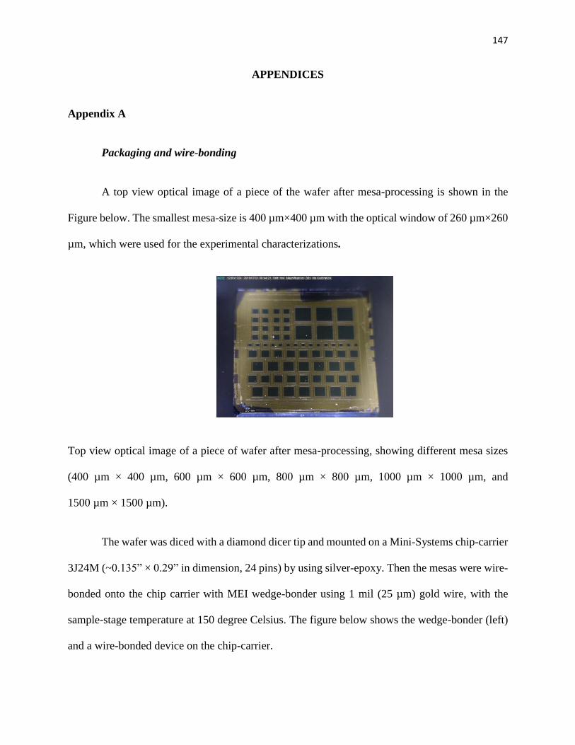
147
APPENDICES
Appendix A
Packaging and wire-bonding
A top view optical image of a piece of the wafer after mesa-processing is shown in the
Figure below. The smallest mesa-size is 400 µm×400 µm with the optical window of 260 µm×260
µm, which were used for the experimental characterizations.
Top view optical image of a piece of wafer after mesa-processing, showing different mesa sizes
(400 µm × 400 µm, 600 µm × 600 µm, 800 µm × 800 µm, 1000 µm × 1000 µm, and
1500 µm × 1500 µm).
The wafer was diced with a diamond dicer tip and mounted on a Mini-Systems chip-carrier
3J24M (~0.135” × 0.29” in dimension, 24 pins) by using silver-epoxy. Then the mesas were wire-
bonded onto the chip carrier with MEI wedge-bonder using 1 mil (25 µm) gold wire, with the
sample-stage temperature at 150 degree Celsius. The figure below shows the wedge-bonder (left)
and a wire-bonded device on the chip-carrier.
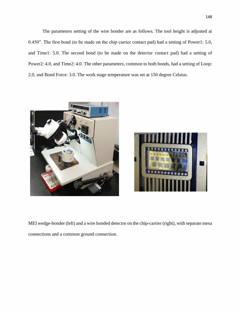
148
The parameters setting of the wire bonder are as follows. The tool height is adjusted at
0.450”. The first bond (to be made on the chip carrier contact pad) had a setting of Power1: 5.0,
and Time1: 5.0. The second bond (to be made on the detector contact pad) had a setting of
Power2: 4.0, and Time2: 4.0. The other parameters, common to both bonds, had a setting of Loop:
2.0, and Bond Force: 3.0. The work stage temperature was set at 150 degree Celsius.
MEI wedge-bonder (left) and a wire bonded detector on the chip-carrier (right), with separate mesa
connections and a common ground connection.

149
Appendix B
Electrical Characterization
The device was mounted on a sample holder of a cryostat cold finger with double shielding
shrouds. After pumping to ~10-6 Torr, the cold finger was cooled by an APD HC2 closed-cycle
refrigerator, which can achieve a temperature as low as 10 K. A computer-controlled Keithley
2635B with a current sensitivity of ~1.3×10⁻¹³A (or 2400 with a current sensitivity of ~10-10A)
source-meter was used to measure the I-V characteristics, with the temperature steps being
controlled by Lakeshore 330 temperature controller.
Block diagram of the electrical characterization set up. The device is mounted on the sample holder
of a cryostat cold finger with double shielding shrouds.

150
Appendix C
Spectral Characterization
A Fourier-transform infrared (FTIR) spectrometer (Perkin Elmer system 2000) is used to
measure the spectral photoresponse signal of the IR detectors. The Perkin Elmer system 2000 uses
Spectrum 5.0 software for the spectral measurements. The FTIR spectrometer consists of a built-
in source of broad IR radiation that is used as the source of IR radiation of the detector
characterization. In order to measure the intensity of the incident IR radiation over a broad spectral
band (NIR through FIR), a bolometer of known sensitivity over the IR spectrum is used. The
bolometer is mounted inside a dewar (HD-3 or HD-5, IR Lab Inc.), where the IR radiation incident
through an IR window of the dewar is focused onto the bolometer by means of a Winston cone
(details in Appendix C). Then the photoresponse signal of the bolometer is measured at liquid
helium temperature. The photoresponse signal from the bolometer electrode contacts is fed to a
voltage pre-amplifier in order to pre-amplify the signal before sending to the computer where the
Spectrum 5.0 software records the spectrum of photoresponse.
The IR detector under test is also mounted inside the dewar in the same way as the
bolometer. The photoresponse signal is recorded in the similar way in the case of bolometer. The
output (raw) signal is then calibrated to obtain the spectral responsivity of the detector under test
as
+=
dL
C
C
S
iRR
RV
GVWAR
11)(
)(
)()/(
, (C.1)
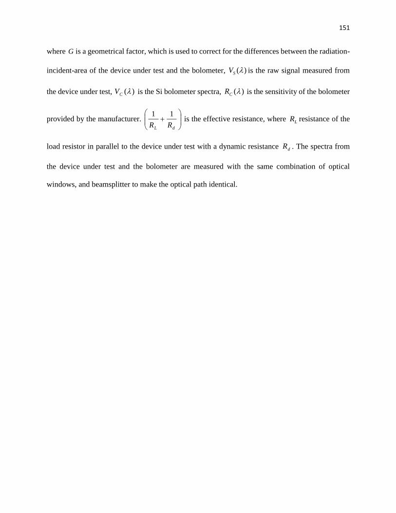
151
where G is a geometrical factor, which is used to correct for the differences between the radiation-
incident-area of the device under test and the bolometer, )(SV is the raw signal measured from
the device under test, )(CV is the Si bolometer spectra, )(CR is the sensitivity of the bolometer
provided by the manufacturer.
+
dL RR
11 is the effective resistance, where LR resistance of the
load resistor in parallel to the device under test with a dynamic resistance dR . The spectra from
the device under test and the bolometer are measured with the same combination of optical
windows, and beamsplitter to make the optical path identical.

152
A block diagram of the spectral photoresponse measurement set up. A long pass optical filter can
be introduced on the path of light to measure selective spectral measurements.
An image of an HDL-5 dewar (IR Lab Inc.) showing IR window for sample illumination.
153
Appendix D
TDIPS fitting by choosing different spectral ranges in the near-threshold region of
extended-wavelength photoresponse
The TDIPS fitting process of a spectral photoresponse curve in the near-threshold region
requires selection of a range of spectrum to be fitted. The experimental quantum yield is used for
the fitting by selecting the spectrum in an energy range Δ1 < < Δ2 such that the energy threshold
lies within this range, where Δ1 is an energy at which the experimental quantum yield spectrum is
flat at background noise level and Δ2 is an energy at which the experimental quantum yield
spectrum is clearly above the background noise level. This background noise level ( 0Y ) is taken
from the experimental quantum yield for each spectrum and its value is usually a small number
(~10-4 to ~10-6). Upper energy limit of the spectrum (Δ2) is an energy at which the experimental
quantum yield spectrum is clearly above the background noise level. For example, in the figure
below shown for the device GSU17I, Δ1 = 0.017 eV is chosen. On the other hand, Δ2 can be chosen
near 0.025 eV or higher as the quantum yield spectrum is seen to be higher than the background
level at these energy values. Since there is no hard and fast rule to choose the value of Δ2, a range
of values are chosen, and the TDIPS fittings are obtained for each case to find the activation energy
Δ. Thus, this process gives a number of fittings on one experimental spectral curve. In order to
evaluate any possible uncertainty in the ΔTDIPS due to error in judgement in the selection of Δ2,
different Δ2 points were selected. For 15SP3 and GSU17I, 11 different Δ2 points were chosen, in
the range of 0.024 to 0.029 eV with 0.0005 eV increments. Similarly, 8 different Δ2 points were
chosen for SP1007 in the range of 0.0245 to 0.028 eV. The TDIPS fittings were also carried out
with two additional Δ2 points at ± 0.00025 eV from the Δ2 corresponding to the minimum χ2 value
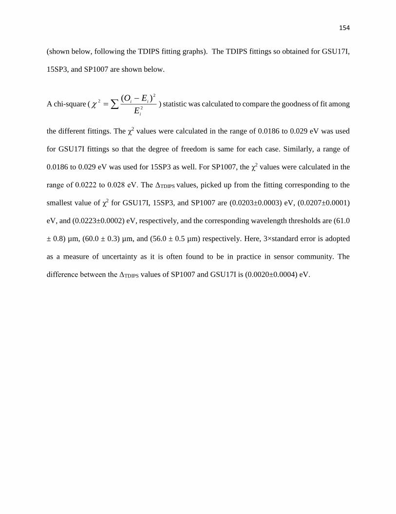
154
(shown below, following the TDIPS fitting graphs). The TDIPS fittings so obtained for GSU17I,
15SP3, and SP1007 are shown below.
A chi-square ( −
=2
2
2 )(
i
ii
E
EO ) statistic was calculated to compare the goodness of fit among
the different fittings. The χ2 values were calculated in the range of 0.0186 to 0.029 eV was used
for GSU17I fittings so that the degree of freedom is same for each case. Similarly, a range of
0.0186 to 0.029 eV was used for 15SP3 as well. For SP1007, the χ2 values were calculated in the
range of 0.0222 to 0.028 eV. The ΔTDIPS values, picked up from the fitting corresponding to the
smallest value of χ2 for GSU17I, 15SP3, and SP1007 are (0.0203±0.0003) eV, (0.0207±0.0001)
eV, and (0.0223±0.0002) eV, respectively, and the corresponding wavelength thresholds are (61.0
± 0.8) µm, (60.0 ± 0.3) µm, and (56.0 ± 0.5 µm) respectively. Here, 3×standard error is adopted
as a measure of uncertainty as it is often found to be in practice in sensor community. The
difference between the ΔTDIPS values of SP1007 and GSU17I is (0.0020±0.0004) eV.
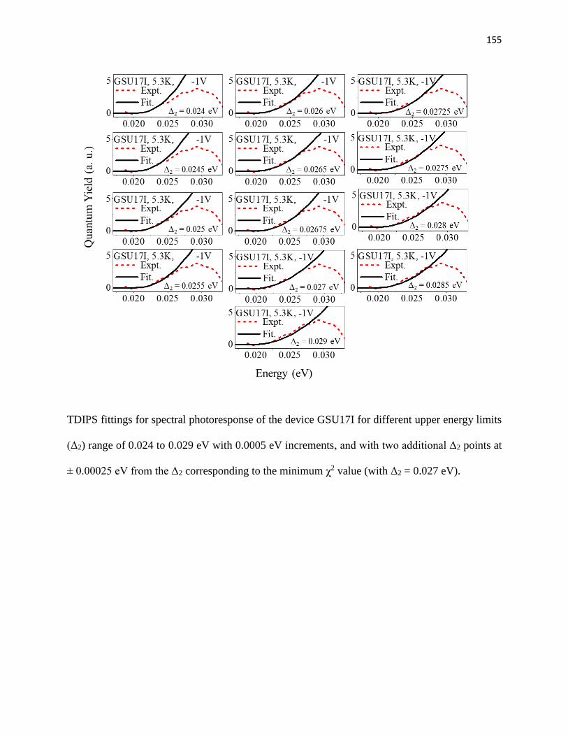
155
TDIPS fittings for spectral photoresponse of the device GSU17I for different upper energy limits
(Δ2) range of 0.024 to 0.029 eV with 0.0005 eV increments, and with two additional Δ2 points at
± 0.00025 eV from the Δ2 corresponding to the minimum χ2 value (with Δ2 = 0.027 eV).
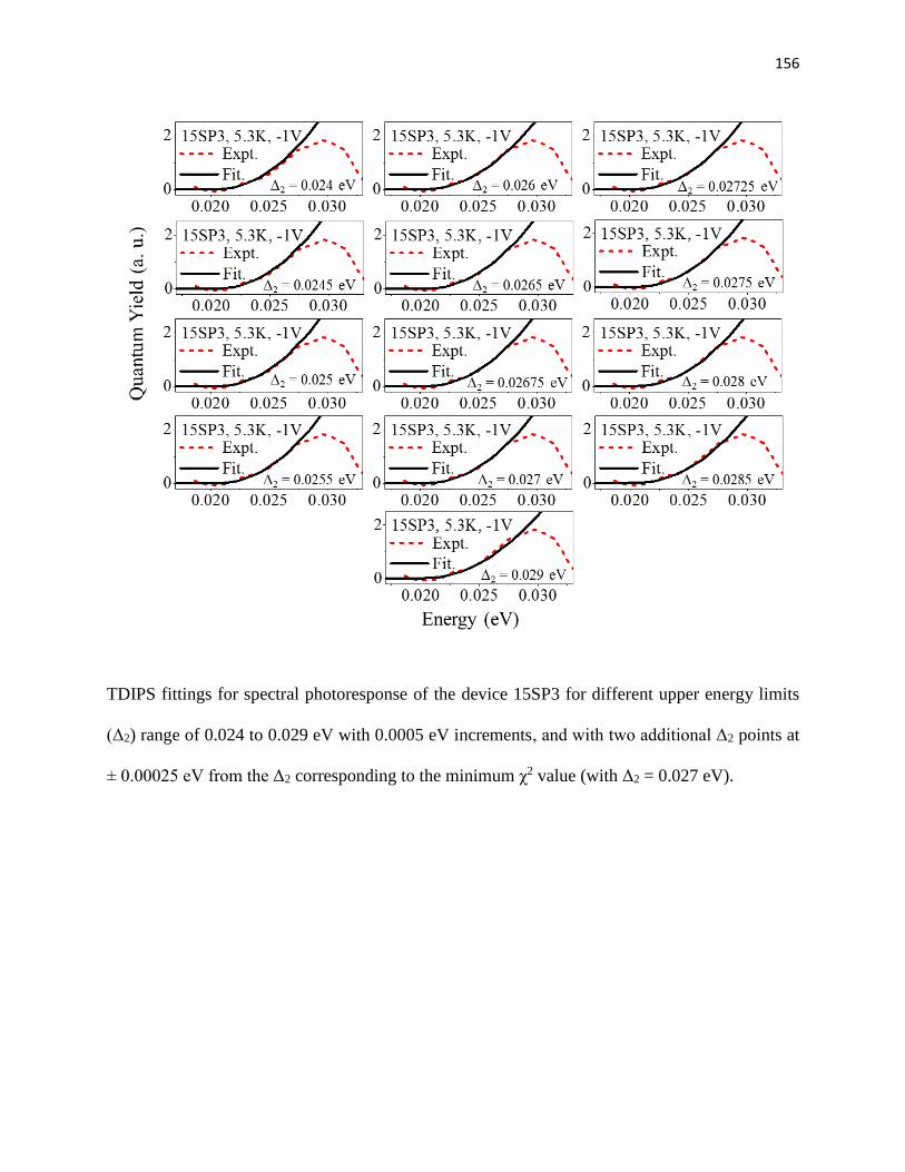
156
TDIPS fittings for spectral photoresponse of the device 15SP3 for different upper energy limits
(Δ2) range of 0.024 to 0.029 eV with 0.0005 eV increments, and with two additional Δ2 points at
± 0.00025 eV from the Δ2 corresponding to the minimum χ2 value (with Δ2 = 0.027 eV).
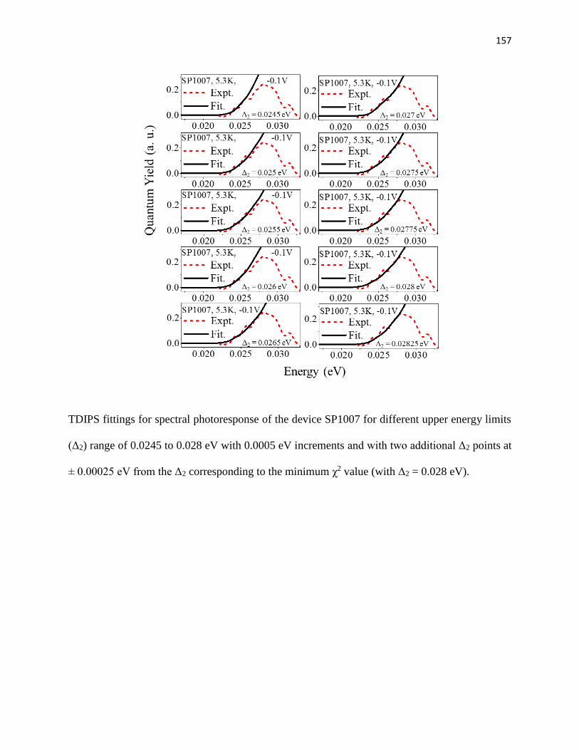
157
TDIPS fittings for spectral photoresponse of the device SP1007 for different upper energy limits
(Δ2) range of 0.0245 to 0.028 eV with 0.0005 eV increments and with two additional Δ2 points at
± 0.00025 eV from the Δ2 corresponding to the minimum χ2 value (with Δ2 = 0.028 eV).
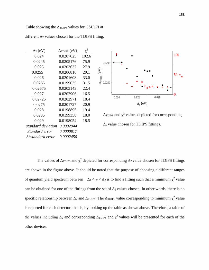
158
Table showing the ΔTDIPS values for GSU17I at
different Δ2 values chosen for the TDIPS fitting.
Δ2 (eV) ΔTDIPS (eV)
χ2
0.024 0.0207025 102.6
0.0245 0.0205176 75.9
0.025 0.0203632 27.9
0.0255 0.0206816 20.1
0.026 0.0201608 33.0
0.0265 0.0199035 31.5
0.02675 0.0203143 22.4
0.027 0.0202906 16.5
0.02725 0.0202971 18.4
0.0275 0.0201727 20.9
0.028 0.0198895 19.4
0.0285 0.0199358 18.0
0.029 0.0198054 18.5
standard deviation 0.0002944 Standard error 0.0000817 3*standard error 0.0002450
The values of ΔTDIPS and χ2 depicted for corresponding Δ2 value chosen for TDIPS fittings
are shown in the figure above. It should be noted that the purpose of choosing a different ranges
of quantum yield spectrum between Δ1 < < Δ2 is to find a fitting such that a minimum χ2 value
can be obtained for one of the fittings from the set of Δ2 values chosen. In other words, there is no
specific relationship between Δ2 and ΔTDIPS. The ΔTDIPS value corresponding to minimum χ2 value
is reported for each detector, that is, by looking up the table as shown above. Therefore, a table of
the values including Δ2 and corresponding ΔTDIPS and χ2 values will be presented for each of the
other devices.
0.024 0.026 0.028
0.0200
0.0205
0
50
100
T
DIP
S (
eV
)
2 (eV)
2
ΔTDIPS and χ2 values depicted for corresponding
Δ2 value chosen for TDIPS fittings.
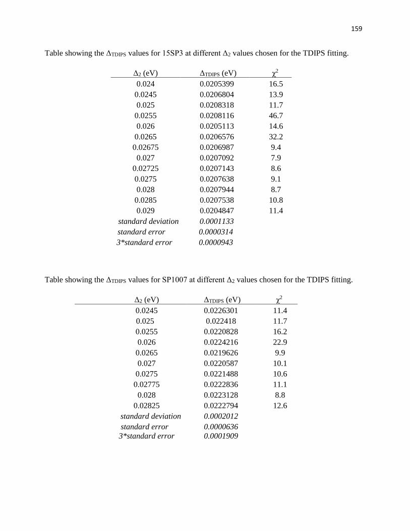
159
Table showing the ΔTDIPS values for 15SP3 at different Δ2 values chosen for the TDIPS fitting.
Δ2 (eV) ΔTDIPS (eV) χ2
0.024 0.0205399 16.5
0.0245 0.0206804 13.9
0.025 0.0208318 11.7
0.0255 0.0208116 46.7
0.026 0.0205113 14.6
0.0265 0.0206576 32.2
0.02675 0.0206987 9.4
0.027 0.0207092 7.9
0.02725 0.0207143 8.6
0.0275 0.0207638 9.1
0.028 0.0207944 8.7
0.0285 0.0207538 10.8
0.029 0.0204847 11.4
standard deviation 0.0001133 standard error 0.0000314
3*standard error 0.0000943
Table showing the ΔTDIPS values for SP1007 at different Δ2 values chosen for the TDIPS fitting.
Δ2 (eV) ΔTDIPS (eV) χ2
0.0245 0.0226301 11.4
0.025 0.022418 11.7
0.0255 0.0220828 16.2
0.026 0.0224216 22.9
0.0265 0.0219626 9.9
0.027 0.0220587 10.1
0.0275 0.0221488 10.6
0.02775 0.0222836 11.1
0.028 0.0223128 8.8
0.02825 0.0222794 12.6
standard deviation 0.0002012 standard error 0.0000636
3*standard error 0.0001909
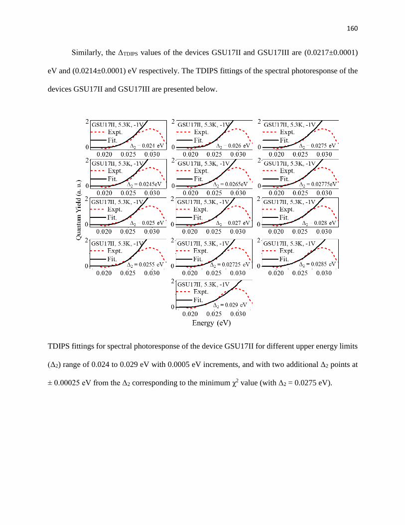
160
Similarly, the ΔTDIPS values of the devices GSU17II and GSU17III are (0.0217±0.0001)
eV and (0.0214±0.0001) eV respectively. The TDIPS fittings of the spectral photoresponse of the
devices GSU17II and GSU17III are presented below.
TDIPS fittings for spectral photoresponse of the device GSU17II for different upper energy limits
(Δ2) range of 0.024 to 0.029 eV with 0.0005 eV increments, and with two additional Δ2 points at
± 0.00025 eV from the Δ2 corresponding to the minimum χ2 value (with Δ2 = 0.0275 eV).
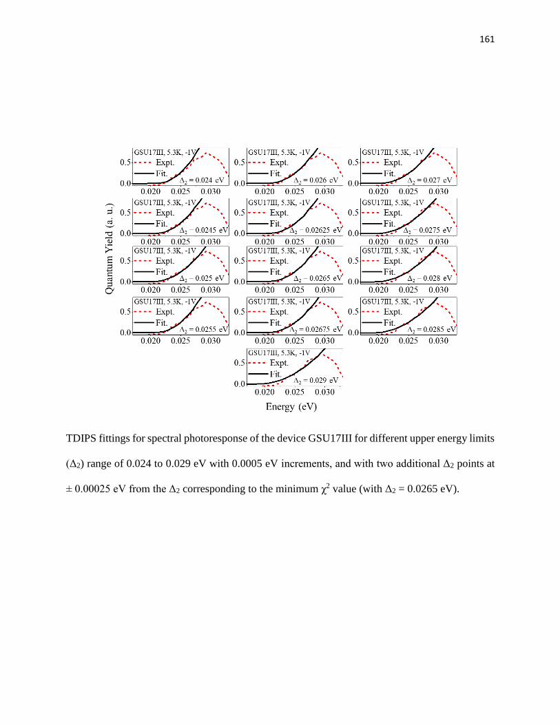
161
TDIPS fittings for spectral photoresponse of the device GSU17III for different upper energy limits
(Δ2) range of 0.024 to 0.029 eV with 0.0005 eV increments, and with two additional Δ2 points at
± 0.00025 eV from the Δ2 corresponding to the minimum χ2 value (with Δ2 = 0.0265 eV).
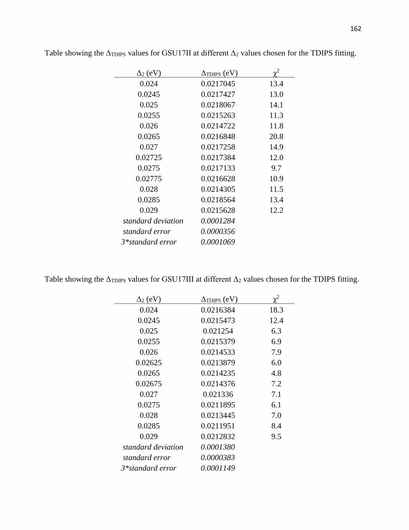
162
Table showing the ΔTDIPS values for GSU17II at different Δ2 values chosen for the TDIPS fitting.
Δ2 (eV) ΔTDIPS (eV) χ2
0.024 0.0217045 13.4
0.0245 0.0217427 13.0
0.025 0.0218067 14.1
0.0255 0.0215263 11.3
0.026 0.0214722 11.8
0.0265 0.0216848 20.8
0.027 0.0217258 14.9
0.02725 0.0217384 12.0
0.0275 0.0217133 9.7
0.02775 0.0216628 10.9
0.028 0.0214305 11.5
0.0285 0.0218564 13.4
0.029 0.0215628 12.2
standard deviation 0.0001284 standard error 0.0000356
3*standard error 0.0001069
Table showing the ΔTDIPS values for GSU17III at different Δ2 values chosen for the TDIPS fitting.
Δ2 (eV) ΔTDIPS (eV) χ2
0.024 0.0216384 18.3
0.0245 0.0215473 12.4
0.025 0.021254 6.3
0.0255 0.0215379 6.9
0.026 0.0214533 7.9
0.02625 0.0213879 6.0
0.0265 0.0214235 4.8
0.02675 0.0214376 7.2
0.027 0.021336 7.1
0.0275 0.0211895 6.1
0.028 0.0213445 7.0
0.0285 0.0211951 8.4
0.029 0.0212832 9.5
standard deviation 0.0001380 standard error 0.0000383
3*standard error 0.0001149
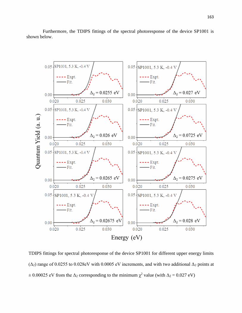
163
Furthermore, the TDIPS fittings of the spectral photoresponse of the device SP1001 is
shown below.
TDIPS fittings for spectral photoresponse of the device SP1001 for different upper energy limits
(Δ2) range of 0.0255 to 0.028eV with 0.0005 eV increments, and with two additional Δ2 points at
± 0.00025 eV from the Δ2 corresponding to the minimum χ2 value (with Δ2 = 0.027 eV)
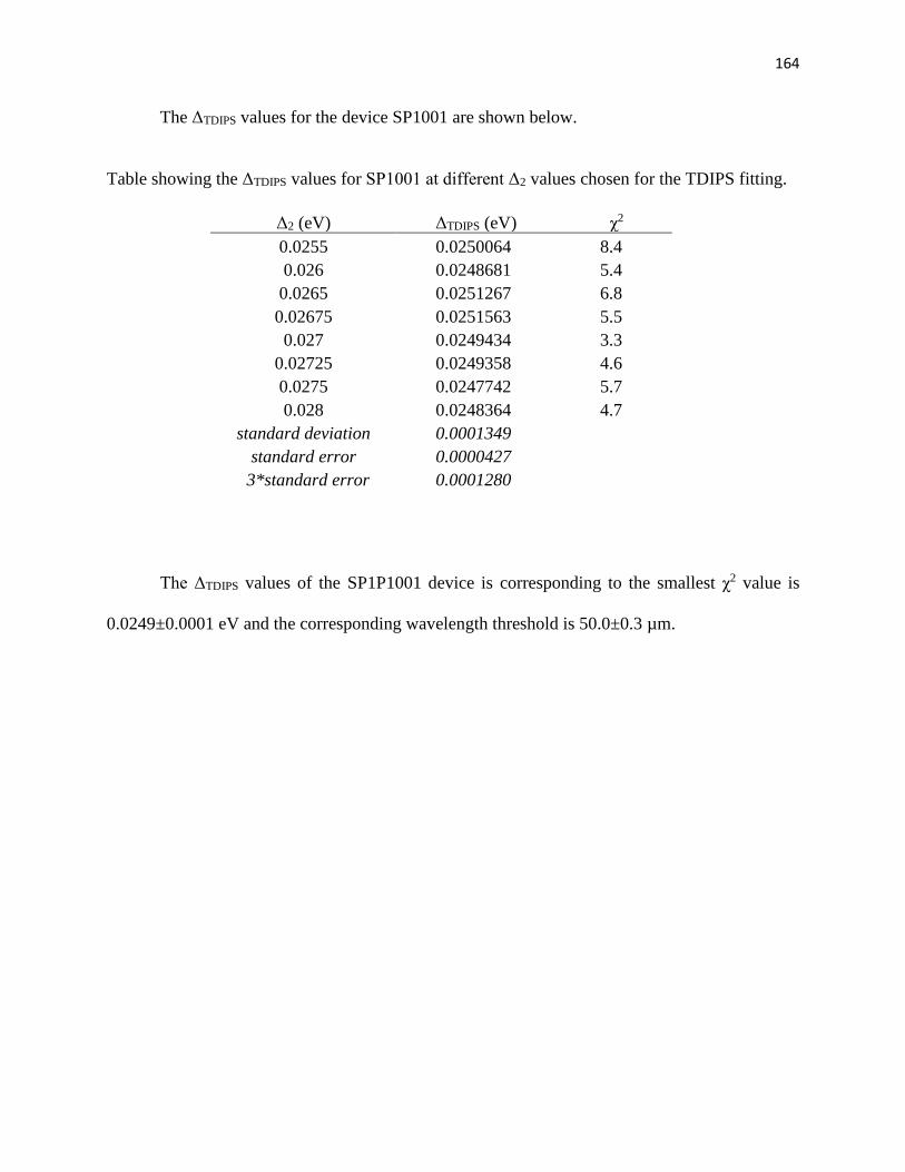
164
The ΔTDIPS values for the device SP1001 are shown below.
Table showing the ΔTDIPS values for SP1001 at different Δ2 values chosen for the TDIPS fitting.
Δ2 (eV) ΔTDIPS (eV) χ2
0.0255 0.0250064 8.4
0.026 0.0248681 5.4
0.0265 0.0251267 6.8
0.02675 0.0251563 5.5
0.027 0.0249434 3.3
0.02725 0.0249358 4.6
0.0275 0.0247742 5.7
0.028 0.0248364 4.7
standard deviation 0.0001349
standard error 0.0000427
3*standard error 0.0001280
The ΔTDIPS values of the SP1P1001 device is corresponding to the smallest χ2 value is
0.0249±0.0001 eV and the corresponding wavelength threshold is 50.0±0.3 µm.
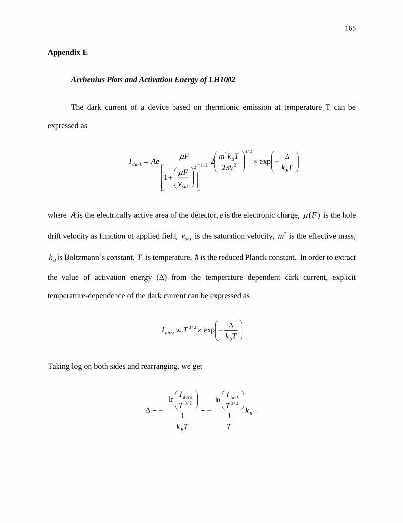
165
Appendix E
Arrhenius Plots and Activation Energy of LH1002
The dark current of a device based on thermionic emission at temperature T can be
expressed as
−
+
=Tk
Tkm
v
F
FAeI
B
B
sat
dark exp2
2
1
2/3
2
*
2/12
where A is the electrically active area of the detector, e is the electronic charge, )(F is the hole
drift velocity as function of applied field, satv is the saturation velocity, *
m is the effective mass,
Bk is Boltzmann’s constant, T is temperature, is the reduced Planck constant. In order to extract
the value of activation energy (Δ) from the temperature dependent dark current, explicit
temperature-dependence of the dark current can be expressed as
−
TkTI
B
dark exp2/3
Taking log on both sides and rearranging, we get
Δ = –
Tk
T
I
B
dark
1
ln2/3
= – B
dark
k
T
T
I
1
ln2/3
.
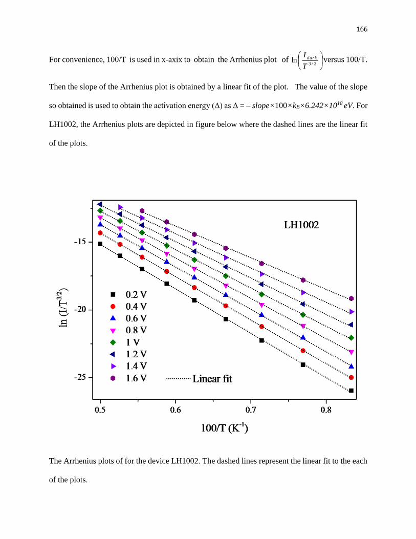
166
For convenience, 100/T is used in x-axix to obtain the Arrhenius plot of
2/3
lnT
I dark versus 100/T.
Then the slope of the Arrhenius plot is obtained by a linear fit of the plot. The value of the slope
so obtained is used to obtain the activation energy (Δ) as Δ = – slope×100×kB×6.242×10¹⁸ eV. For
LH1002, the Arrhenius plots are depicted in figure below where the dashed lines are the linear fit
of the plots.
The Arrhenius plots of for the device LH1002. The dashed lines represent the linear fit to the each
of the plots.
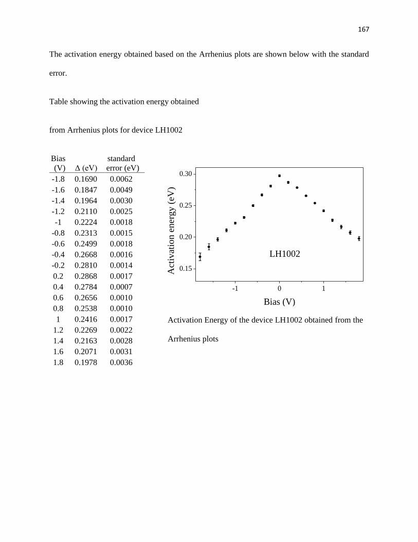
167
The activation energy obtained based on the Arrhenius plots are shown below with the standard
error.
Table showing the activation energy obtained
from Arrhenius plots for device LH1002
Bias
(V) Δ (eV)
standard
error (eV)
-1.8 0.1690 0.0062
-1.6 0.1847 0.0049
-1.4 0.1964 0.0030
-1.2 0.2110 0.0025
-1 0.2224 0.0018
-0.8 0.2313 0.0015
-0.6 0.2499 0.0018
-0.4 0.2668 0.0016
-0.2 0.2810 0.0014
0.2 0.2868 0.0017
0.4 0.2784 0.0007
0.6 0.2656 0.0010
0.8 0.2538 0.0010
1 0.2416 0.0017
1.2 0.2269 0.0022
1.4 0.2163 0.0028
1.6 0.2071 0.0031
1.8 0.1978 0.0036
-1 0 1
0.15
0.20
0.25
0.30A
cti
vati
on
en
erg
y (
eV
)
Bias (V)
LH1002
Activation Energy of the device LH1002 obtained from the
Arrhenius plots
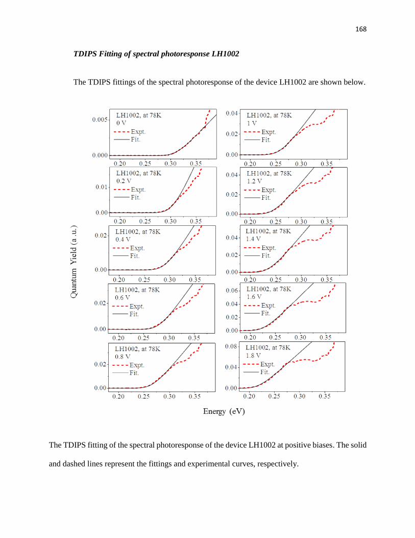
168
TDIPS Fitting of spectral photoresponse LH1002
The TDIPS fittings of the spectral photoresponse of the device LH1002 are shown below.
The TDIPS fitting of the spectral photoresponse of the device LH1002 at positive biases. The solid
and dashed lines represent the fittings and experimental curves, respectively.
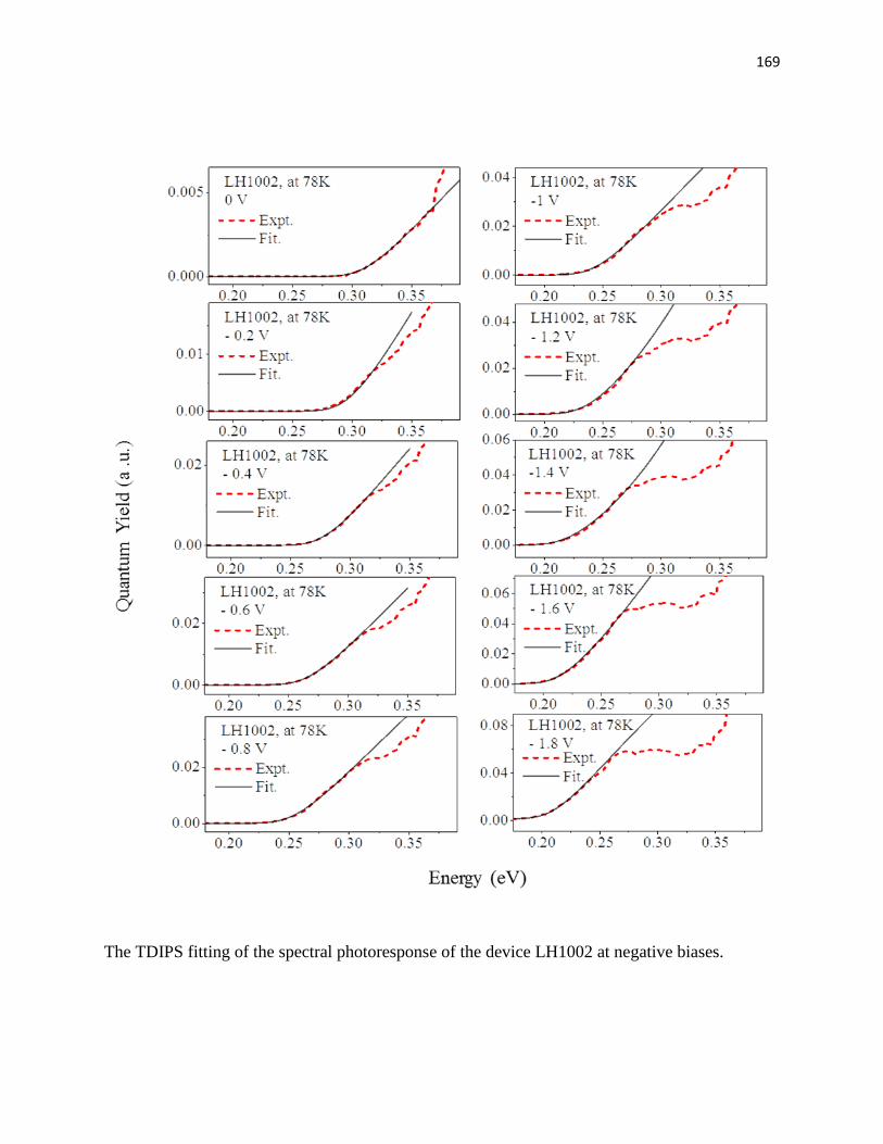
169
The TDIPS fitting of the spectral photoresponse of the device LH1002 at negative biases.
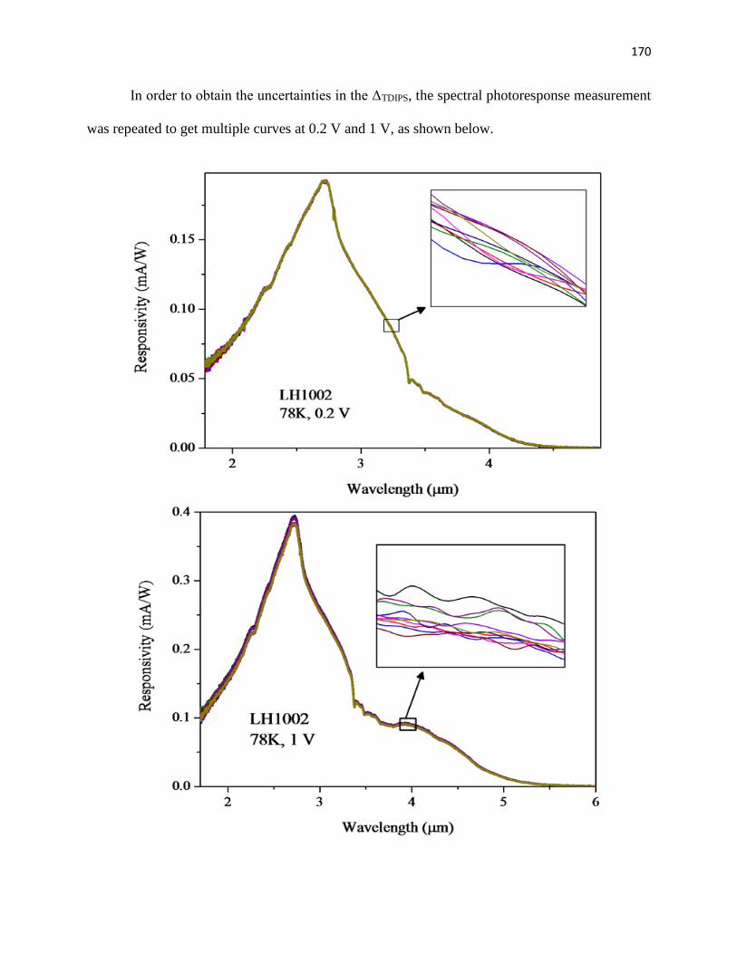
170
In order to obtain the uncertainties in the ΔTDIPS, the spectral photoresponse measurement
was repeated to get multiple curves at 0.2 V and 1 V, as shown below.

171
Multiple spectral photoresponse curves (10 each) at 0.2 V (top panel) and 1 V (bottom panel). The
insets show the zoomed in section to show the multiple curves.
The ΔTDIPS values from 10 curves each at 0.2 V and 1 V for the device LH1002 are shown below.
ΔTDIPS (eV)
0.2 V 1 V
0.2827032 0.2417796
0.2824678 0.2418151
0.2831114 0.2416721
0.2843925 0.2415248
0.2841176 0.2420442
0.2836154 0.2417660
0.2842717 0.2412862
0.2834729 0.2419682
0.2839264 0.2424358
0.2837816 0.2419122
standard deviation 0.000652002 0.0003088
standard error 0.000206181 0.0000977
3*standard error 0.000618544 0.0002930
Based on these results, the wavelength thresholds are (4.37 ±0.01) µm, and (5.13 ±0.01) µm at
0.2 V and 1 V respectively. Since the uncertainty in the wavelength threshold is consistently small,
±0.01 µm may be adopted for the device LH1002 at all biases.
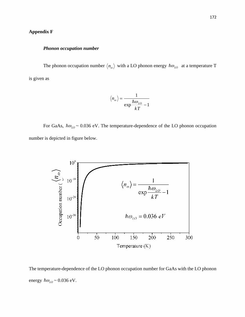
172
Appendix F
Phonon occupation number
The phonon occupation number n with a LO phonon energy LO at a temperature T
is given as
1exp
1
−
=
kT
nLO
For GaAs, LO ~ 0.036 eV. The temperature-dependence of the LO phonon occupation
number is depicted in figure below.
The temperature-dependence of the LO phonon occupation number for GaAs with the LO phonon
energy LO ~ 0.036 eV.
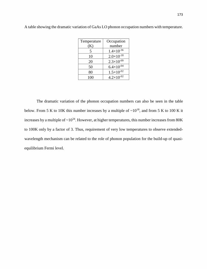
173
A table showing the dramatic variation of GaAs LO phonon occupation numbers with temperature.
Temperature
(K)
Occupation
number
5 1.4×10-36
10 2.0×10⁻¹⁸
20 2.3×10-09
50 6.4×10-04
80 1.5×10-02
100 4.2×10-02
The dramatic variation of the phonon occupation numbers can also be seen in the table
below. From 5 K to 10K this number increases by a multiple of ~1018, and from 5 K to 100 K it
increases by a multiple of ~1034. However, at higher temperatures, this number increases from 80K
to 100K only by a factor of 3. Thus, requirement of very low temperatures to observe extended-
wavelength mechanism can be related to the role of phonon population for the build-up of quasi-
equilibrium Fermi level.