master thesis - universitetet i...
TRANSCRIPT

UNIVERSITY OF OSLO
Department of informatics
CMOS Microwave LNA design
Master thesis 60 credits
Mats Risopatron Knutsen
June 1
st 2010
CMOS Microwave LNA design
2

June 1st 2010
3
Abstract
In 2002, the FCC released an unlicensed UWB frequency band from 3.1 GHz to 10.6 GHz. This
frequency band opens for new wireless applications. Most wireless applications need analog
front-end for interfacing the antenna, often in the form of a wideband microwave LNA.
This thesis will address some of the main aspects of microwave LNA design for use in the UWB
frequency band. Trough evaluation of the published literature on the subject, a circuit topology
has been selected, explored and redesigned. The tradeoffs concerning input- and output match,
bandwidth and gain has been explored and discussed.
As a part of this thesis four prototype UWB LNAs have been developed, using a minimum of
inductors to maintain the bandwidth, gain and matching properties. These LNAs shows
promising results in post-layout simulations. The achieved simulation result is 15.1dB gain with a
-3 dB bandwidth of 0.4- to 8.6 GHz and a NF below 5.8 dB. The proposed LNAs circuits should be
of great interest for further development in microwave and UWB systems.

CMOS Microwave LNA design
4

June 1st 2010
5
Contents Abstract ............................................................................................................................................ 3
List of figures .................................................................................................................................... 7
List of tables ...................................................................................................................................... 9
Acronyms ........................................................................................................................................ 11
Acknowledgement .......................................................................................................................... 13
1 Introduction ................................................................................................................................. 15
1.1 Goal of this thesis ................................................................................................................. 15
1.2 Motivation ............................................................................................................................ 15
1.3 Field of application ............................................................................................................... 16
1.4 The making this thesis .......................................................................................................... 16
1.5 Outline of the thesis ............................................................................................................. 17
2 Introduction to UWB and fundamental microwave theory ........................................................ 19
2.1 Chapter overview ................................................................................................................. 19
2.2 A short historical summary from the birth of RF to modern UWB ...................................... 19
2.3 Transmission lines and impedance matching ....................................................................... 20
2.3.1 Transmission lines ......................................................................................................... 20
2.3.2 Characteristic impedance .............................................................................................. 21
2.3.3 Reflections and impedance matching ........................................................................... 22
2.3.4 The Smith chart ............................................................................................................. 24
2.4 Input impedance matching techniques ................................................................................ 27
2.5 Noise factor and noise figure ............................................................................................... 29
2.6 Bond wire and pad characterization .................................................................................... 30
3 Evaluation of the architectures ................................................................................................... 33
3.1 Chapter overview ................................................................................................................. 33
3.2 LNA design strategies ........................................................................................................... 33
3.2.1 Process challenges ......................................................................................................... 33
3.2.2 Bandwidth enhancement techniques ........................................................................... 34
3.3 UWB LNA architectures ........................................................................................................ 38
3.3.1 Generic architectures .................................................................................................... 38

CMOS Microwave LNA design
6
3.3.2 Explored architectures .................................................................................................. 44
4 Circuit implementation ............................................................................................................... 53
4.1 Chapter overview ................................................................................................................. 53
4.2 The architecture chosen and specification goals ................................................................. 53
4.3 Implemented LNAs ............................................................................................................... 53
4.3.1 LNA architecture 1 ........................................................................................................ 54
4.3.2 LNA architecture 2 ........................................................................................................ 57
4.3.3 LNA architecture 3 ........................................................................................................ 60
4.3.4 LNA architecture 4 ........................................................................................................ 66
4.3.5 Input match ................................................................................................................... 69
4.3.6 Output match ................................................................................................................ 70
4.3.7 Layout versus schematic ............................................................................................... 71
4.4 Simulated performance summary ....................................................................................... 72
4.5 Layout ................................................................................................................................... 74
4.5.1 Pad frame ...................................................................................................................... 74
4.5.2 Layout strategies ........................................................................................................... 76
5 Measurements ............................................................................................................................ 83
5.1 Chapter overview ................................................................................................................. 83
5.2 Measurements ..................................................................................................................... 83
5.2.1 Printed circuit board design .......................................................................................... 83
5.2.2 Measurements setup .................................................................................................... 85
5.2.3 Measurement result ..................................................................................................... 86
6 Conclusion an proposal for future work ..................................................................................... 97
6.1 Conclusion ............................................................................................................................ 97
6.2 Future work .......................................................................................................................... 97
APPENDIX A: Layout of LNA 2 ........................................................................................................ 99
APPENDIX B: Layout of LNA 3 ...................................................................................................... 101
APPENDIX C: Layout of LNA 4 ...................................................................................................... 103
References ................................................................................................................................... 105

June 1st 2010
7
List of figures Figure 1: Unit transmission line element ....................................................................................... 21
Figure 2: Smith Chart, from [Ludw 09] ........................................................................................... 25
Figure 3: Block scheme of two port analysis .................................................................................. 26
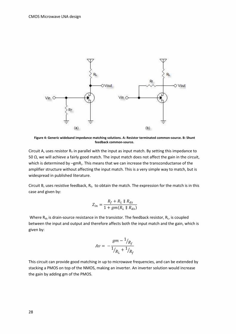
Figure 4: Generic wideband impedance matching solutions. A: Resistor terminated common-
source. B: Shunt feedback common-source. .................................................................................. 28
Figure 5: High frequency, wide band matching approaches. A: inductor degenerated common
source. B: Common-gate ................................................................................................................ 29
Figure 6: Series peaked common source amplifier ........................................................................ 35
Figure 7: Shunt-peaked common source amplifier ........................................................................ 36
Figure 8: T-coiled enhanced common source amplifier ................................................................. 37
Figure 9: Common source amplifier ............................................................................................... 39
Figure 10: Small signal equivalent of a source degenerated transistor ......................................... 39
Figure 11: Common gate amplifier ................................................................................................. 40
Figure 12: Small signal equivalent .................................................................................................. 41
Figure 13: Cascaded amplifier stages ............................................................................................. 42
Figure 14: Distributed amplifier, from [Haji 03] ............................................................................. 43
Figure 15: Source degenerated common source amplifier, [Bevi 04] ............................................ 44
Figure 16: Common gate amplifier with interstage matching network [Stan 05] ......................... 46
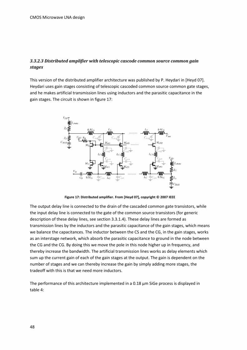
Figure 17: Distributed amplifier. From [Heyd 07], copyright © 2007 IEEE .................................... 48
Figure 18: Inverter based amplifier using splitting-load inductive peaking technique [Chao 08] . 49
Figure 19: Simulated gain performance of single state inverters. From [Chao 08], copyright ©
2008 IEEE ........................................................................................................................................ 50
Figure 20: Schematic LNA 1 ............................................................................................................ 54
Figure 21: Layout simulated, S11 and S22, of LNA 1 ......................................................................... 55
Figure 22: Layout simulated S21 and S12, of LNA 1 .......................................................................... 56
Figure 23: Layout simulated NF of LNA 1 ....................................................................................... 57
Figure 24: Schematic LNA 2 ............................................................................................................ 58
Figure 25: Post-layout simulated S11 and S22, of LNA 2 .................................................................. 58
Figure 26: Post-layout simulated S21 and S12, of LNA 2 .................................................................. 59
Figure 27: Post-layout simulated NF of LNA 2 ................................................................................ 60
Figure 28: Schematic LNA 3 ............................................................................................................ 61
Figure 29: Post-layout versus schematic S22 simulations of LNA 3 ................................................. 61
Figure 30: Post-layout versus schematic S22 simulations of LNA 3 ................................................. 62
Figure 31: Post-layout simulated S11 and S22, of LNA 3 ................................................................... 63
Figure 32: Post-layout simulated S21 and S12, of LNA 3 .................................................................. 64
Figure 33: Post-layout simulated NF of LNA 3 ................................................................................ 65
Figure 34: Schematic LNA 4 ............................................................................................................ 66
Figure 35: Post-layout simulated S11 and S22 of LNA 4 ................................................................... 67

CMOS Microwave LNA design
8
Figure 36: Post-layout simulated S21 and S12 of LNA 4 ................................................................... 68
Figure 37: Post-layout simulated NF of LNA 4 ............................................................................... 69
Figure 38: Post-layout simulated S11, series match versus splitting load technique ..................... 70
Figure 39: Post-layout simulated S22, no inductor versus inductor at NMOS and inductor in series
....................................................................................................................................................... 71
Figure 40: Simulated power gain, S21, of LNA 1 in schematic and post-layout .............................. 72
Figure 41: Pad frame of master chip .............................................................................................. 74
Figure 42: Pad frame test chip ....................................................................................................... 75
Figure 43: Layout of LNA 1 ............................................................................................................. 76
Figure 44: Decoupling included in the LNA layouts ....................................................................... 77
Figure 45: Layout of RF NMOS provided by the design kit ............................................................ 78
Figure 46: Cross section deep n-well NMOS, from [Dahl 09] ........................................................ 79
Figure 47: Inductor on chip with metal grid .................................................................................. 80
Figure 48: Cross-section of a PCB with microstrip line .................................................................. 83
Figure 49: PCB of master chip ........................................................................................................ 84
Figure 50: PCB of test chip ............................................................................................................. 85
Figure 51: Measurement setup, inspirited by [Dahl 09] ................................................................ 86
Figure 52: Measured S11 and S22 of LNA 1 ...................................................................................... 87
Figure 53: Measured S21 and S12 of LNA1 ....................................................................................... 88
Figure 54: Measured S11 and S22 of LNA 2 ...................................................................................... 89
Figure 55: Measured S21 and S12 of LNA 2 ...................................................................................... 90
Figure 56: Measured S21 and S12 of LNA 4 ...................................................................................... 91
Figure 57: Measured S21 and S12 of LNA 4 ...................................................................................... 92
Figure 58: Measured S11 of shorted and open bond wire test benches implemented on master
chip ................................................................................................................................................. 94
Figure 59: Calculated absolute value of impedance in bond wire of master chip using W. C.
Johnson Formula ............................................................................................................................ 94
Figure 60: Measured S11 of shorted and open bond wire test benches implemented on test chip
....................................................................................................................................................... 95
Figure 61: Calculated absolute value of impedance in bond wire of test chip using W. C. Johnson
Formula .......................................................................................................................................... 96

June 1st 2010
9
List of tables Table 1: List of reflection coefficient with the equivalent RL and SWR ......................................... 24
Table 2: Performance of source degenerated common source amplifier ..................................... 45
Table 3: Performance of common gate amplifier with interstage matching network .................. 47
Table 4: Performance of distributed amplifier with telescopic cascode common source common
gain stages ...................................................................................................................................... 49
Table 5: Performance of inverter based amplifier using splitting-load inductive peaking technique
........................................................................................................................................................ 51
Table 6: Summary of simulated performance and brief comparison with measured state-of-the-
art publications ............................................................................................................................... 73

CMOS Microwave LNA design
10
June 1st 2010
11
Acronyms
BW BandWidth
DUT Device Under Test
Bi-CMOS Bipolar Complementary Metal Oxide Semiconductor
CMOS Complementary Metal-Oxide Semiconductor
CG Common Gate
CS Common Source
DRC Design Rule Check
EIRP Equivalent Isotropically Radiated Power
FCC Federal Communications Commission
FR4 Flame Resistant 4
GBW Gain-BandWidth product
GPS Global Positioning System
LNA Low Noise Amplifier
LOD Length of Oxide Definition
MOSFET Metal-Oxide Semiconductor Field-Effect Transistor
NMOS N-Channel MOSFET
PCB Printed Circuit Board
PLS Post-Layout Simulation
PMOS P-Channel MOSFET

CMOS Microwave LNA design
12
QFN Quad Flat No leads
Radar RAdio Detection And Ranging
RF Radio Frequency
RL Return Loss
SiGe Silicon-Germanium
SMA Sub-Miniature version A
SNR Signal-to-Noise Ratio
S-parameters Scattering Parameters
STI Shallow Trench Isolation
SWR Standing Wave Ratio
UWB Ultra WideBand
VIA Vertical Interconnect Access
WPE Well edge Proximity Effect
June 1st 2010
13
Acknowledgement
First I would like to thank my supervisor Tor Sverre Lande for accepting me as his student, and
for excellent guidance and encouragement throughout the one and a half years this work has
been developed.
Great thanks to my co-supervisors Kristian Granhaug and Håkon André Hjortland for providing
technical skills, guidance and morale-boosts throughout this work.
Olav Stanly Kyrvestad deserves special thanks for sticking out with me throughout the chip tape
out, and for always keeping the spirits up. A special thank to Øyvind Næss how has been as a co-
supervisor during the last year.
Thank you Stig Holm Rogne and Ole Petter Haneborg for some of the best exam preparation
periods and table tennis sessions ever.
I owe great thanks to the guys at the lab, Amir, Dag, Geir and Tor-Eivind for making the days at
the MES lab more enjoyable and full of caffeine. Both social and technical discussions have
improved this thesis. Tanks to Anh Tuan Vu for great lab guidance and PCB design.
Last, but not least I would like to thank the Novelda crew, Kjetil, Olav, Claus, Dag, Nikolaj, Stig,
Aage and Kristian for willingly sharing of all your knowledge and experience.

CMOS Microwave LNA design
14
June 1st 2010
15
1 Introduction
1.1 Goal of this thesis
The goal of this thesis is to explain the fundamentals of microwave Low Noise Amplifier (LNA)
design for use in the Ultra Wide frequency Band (UWB), to illustrate and discuss some of the
tradeoffs we are faced upon during the design phase of making a UWB LNA in a modern
production process, and to develop a prototype UWB LNA in 90nm Complementary Metal-Oxide
Semiconductor (CMOS) technology. This thesis will hopefully contribute to enhance the
knowledge of UWB LNAs, bond wiring and pad properties, and point out the importance of
impedance matching microwave CMOS circuits.
1.2 Motivation
The focus and development of UWB wireless communication applications and wireless sensor
systems has been increasing since 2002 when the Federal Communications Commission (FCC)
released the UWB mask. The UWB mask stretches from 3.1 GHz to 10.6 GHz with an allowed
Equivalent Isotropically Radiated Power (EIRP) emission level at -41.3 dBm/MHz (part 15 limit).
This is the widest unlicensed frequency band ever to be released. The low emission levels
allowed by FFC, somewhat limits the applications to low power short range communication, but
it also opens new doors with respect to impulse radio which pulses benefits from the large
bandwidth. The advantage and potential of UWB technology can be seen form Shannon’s link
capacity formula:
= ∗ (1 + )
Where C is the channel capacity, B is the bandwidth and SNR is the signal-to-noise ratio in the
channel. As we see the link capacity is linearly proportional to the bandwidth and follows a
logarithmic relation with the signal-to-noise ratio. With large bandwidth we can achieve high
data rates with very small radiated power (little radiated power equals a poor SNR in a wireless
link).
Almost all wireless system needs some sort of analog front-end, generally in the form of a LNA,
to interface the antenna. CMOS technology is the most widespread technology used in

CMOS Microwave LNA design
16
integrated circuits. This technology is originally developed for digital solutions, and is not
optimized for analog microwave design. Implementing UWB front-end in modern nanometer
CMOS technology is a challenge in more than one way. We want to exploit the great bandwidth
released by the FCC, and at the same time maintain low power consumption and minimize the
area to reduce production costs. Low power consumption is one of the main focus points in
modern electronics and is necessary to make implementation in handheld battery operated
devices possible and practical. Advanced processes limit the number of amplifier topologies that
can be used, and according to Willy Sansen [Sans 05], CMOS processes technologies under 0.180
µm are unsuited for microwave design. This due to the reduced supply voltage and the poor
noise properties we achieve in these processes. Area on-chip is costly, and therefore it is
desirable to use as little possible. Inductors are large on-chip, and therefore becomes a luxury
we only use where they are really needed. To avoid all these obstacles new amplifier topologies
and design approaches has to be explored.
1.3 Field of application
The microwave/UWB front-end topologies discussed and explored in this thesis has a wide
variety of possible applications. These applications stretch from high bit-rate wireless
audio/video transmissions, medical imaging, and wireless sensor networks to military
applications and high precision location applications.
Even in a radio system were the UWB frequency band is divided into many narrow bands we
need a broadband LNA. This is because of the restrictions in the allowed transmitted power are
so tight that pre processing/filtering before the LNA is difficult.
1.4 The making this thesis
This research effort is carried out between January 2009 and June 2010, the work has more or
less been divided into two main phases.
Phase 1 mainly consisted of studying UWB and microwave literature to gain an understanding of
the field, and to get an overview of different reported topologies realized in CMOS and Bipolar
Complementary Metal Oxide Semiconductor (Bi-CMOS). This phase consumed most of the first
six months of the work.
Phase 2 was the design phase. Here several of the most promising architectures and design
strategies from phase 1 were explored in detail, and schematic and layout simulations were
carried out. The architectures with the best performance were implemented on chip and sendt
to Taiwan Semiconductor Manufacturing Company (TSMC), for production in 90nm CMOS

June 1st 2010
17
technology.
1.5 Outline of the thesis
This thesis will consist of three main parts. Firstly the theory part, which forms the basis the
reader needs to understand the choices made further out in the thesis. Secondly the literature
evaluation part, where different amplifier topologies are discussed and evaluated. The last part
is the prototype development which includes the steps from schematic to chip measurements.
Here is an overview of the following chapters:
Chapter 2 will cover the basic theory of microwave and UWB LNA design. S-parameters and
impedance matching among other things will be described here.
Chapter 3 will direct the theory towards the challenges and tradeoffs when designing wideband
microwave LNAs. Bandwidth enhancement techniques and generic high frequency amplifier
topologies will be presented. Chapter 3 will present and discuss some of the architectures that
were under consideration after the literature study phase.
Chapter 4 will in detail present the four LNA circuits that eventually ended up on chip, and their
simulated performance. Layout techniques used when designing the LNAs will be presented.
Chapter 5 presents the PCB, measuring setup and measured results of the proposed circuits. The
results will be evaluated and discussed in this chapter.
In Chapter 6 we conclude the thesis and present suggestions for future work.

CMOS Microwave LNA design
18
June 1st 2010
19
2 Introduction to UWB and fundamental microwave theory
The term ultra-wide band is used for frequency bands that are wider than 500 MHz. Recently
unlicensed ultra-wide frequency bands have been released for commercial use in the U.S. (3.1-
10.6 GHz) and Europe (6-8.5 GHz). These wide frequency bands open for new and exciting
wireless application. A key component in many of these wireless systems is the analog front-end
doing the initial signal processing. Microwave Low Noise Amplifiers (LNA) is subject to effects
that only occur at high frequencies. This chapter will present the fundamental microwave theory
necessary as background material for the rest of the thesis.
2.1 Chapter overview
The first part of this chapter will present a brief history of RF and UWB. Next we will explore
some of the characteristics of microwave theory and how this affects us when designing
microwave LNAs in nanometer scale CMOS technology.
2.2 A short historical summary from the birth of RF to modern UWB
The first transmission and reception of electromagnetic waves was conducted by Henrich Hertz
in 1887. Hertz used a spark-gap transmitter, i.e. transmitting impulses, and were able to transmit
an impulse over a few meters. In 1901 Guglielmo Marconi, one of the big pioneers of radio,
transmitted Morse-code over a longer distance. Morse-code was also based on the transmission
of impulses. Impulses have a wide bandwidth, so we can say that the first wireless transmission
was wideband impulse-based transmissions.
The weakness of the early age, impulse based, communication was the interference when the
number of user increased. To counteract the interference problematic, frequency modulated
transmission emerged. These frequency modulated transmission used a narrower frequency
band but still achieved a SNR superior to the Morse code. Frequency modulated wireless
transmission is still used today in most wireless systems.
In 2002 FCC defined a UWB mask (3.1GHz – 10.6 GHz) allowing for transmission, with some
restrictions, in this frequency band. This UWB mask opens for new applications, some of which
state-of-the-art solutions transmit impulses, so we are in some ways turning back to the starting
point of wireless transmission.

CMOS Microwave LNA design
20
2.3 Transmission lines and impedance matching
Analog low-frequency designers are often surprised by the RF and microwave designers’
obsession with impedance matching. In much of the low-frequency applications voltage gain
rather than power gain is the dominating parameter, this implies that there is more than enough
power available in the input signal. Power gain is the dominating parameter in microwave
amplifier design, this due to the fact that there usually is very small amount of power in the
signal. Form basic electronic theory we know that maximum power transfer occurs when the
source and load resistance is matched.
Maximized power transfer is not the only reason for striving for impedance match in microwave
circuits. At microwave frequencies lumped models for all interconnects are no longer valid, the
traces on Printed Circuit Boards (PCB) and off-chip interconnects has to treated as distributed
models. PCB traces and interconnects used for microwave frequencies operate with a
characteristic impedance. This is the impedance of the interconnects at high frequencies. By
matching the chip’s input and output impedances with this characteristic impedance we
minimize the effect of the external interconnects.
2.3.1 Transmission lines
Transmission line is the common notion for high frequency signal paths. When designing UWB
LNAs in nanometer silicon technology we have to use transmission lines to interconnect with
antennas and other external components. Transmission lines used at these frequencies have
properties which we need to know about, and design our LNA to match.
A rule of tomb is that if wavelength of the transferred signal exceeds one tenth of the
interconnect length, we have to use transmission line theory to evaluate the interconnect. The
wavelength, λ, of the signal is given by:
=
Where f is the frequency of the signal and Vp is the propagation velocity in the transmission line.
The propagation velocity in the transmission line is given by:
= √∗
June 1st 2010
21
Were equals the dielectric constant of the material used in the transmission line and µ
equals permeability, which is in most cases simplified to 1. C is the speed of light in vacuum
(3*10^8 m/s), which is approximately the same as the speed of electromagnetic waves in
vacuum. of the transmission line will always be larger or equal to the dielectric constant of
vacuum, and we can derive from this equation that <C always.
Form the equation above we see that the wavelength in a medium always is longer than the
wavelength in vacuum. A disturbing fact is that the wavelength in a CMOS process, which has
=11.7 and µ =1, at 10 GHz is roughly 8.8 mm. It is quite obvious that in near future
transmission line phenomena will occur even internally on chip, which until now has not been an
issue for microwave designers.
2.3.2 Characteristic impedance
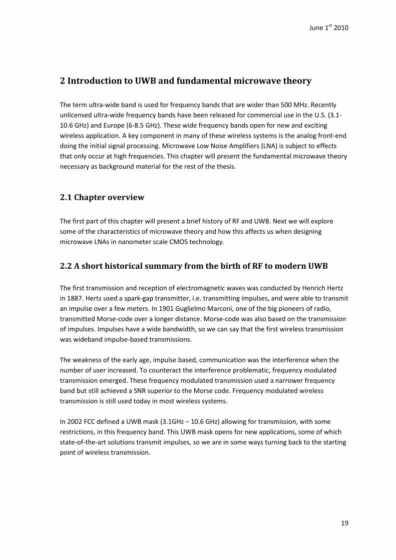
The key feature of the transmission line is its characteristic impedance, Z0. This is the high
frequency impedance of the transmission line. Figure 1 shows a lumped model of a transmission
line unit element:
Figure 1: Unit transmission line element
A transmission line will consist of infinite number of these transmission line elements. In figure 1
R is the series resistance per unit length, L is the series inductance per unit length, G is
conductance of the dielectric per unit length and C is the capacitance between the conducting
wire and the return path. R and G represent the loss elements in the transmission line. This
model gives an intuitive picture of the transmission line segment, and allow analysis using
Kirchhoff’s current and voltage laws. Based on the model in figure 1, we can express the
characteristic impedance, , as:

CMOS Microwave LNA design
22
= !"#$%&'#$%
At high frequencies the series inductance and parallel capacitance in the fraction becomes
dominating. Then the expression can be simplified to:
= !"#$%&'#$% ~)!$%&
$% = !&
This is the fundamental expression for the characteristic impedance in a transmission line. Even
though this is a simplified expression of a simplified model, it is widely used as an estimator in
scientific circles. For more correct and complex models and expression for Z0, see [Ludw 09] or
[1Lee 04].
The use of characteristic impedances affects us when designing microwave LNAs in silicon. The
input and output of the chip has to be matched to the characteristic impedance of the system to
avoid reflections and maximize the power transfer. The characteristic impedance used in most
measurement equipment and discrete microwave devices is 50 Ω. The use of 50 Ω is based on
the fact that this value is close to the geometric and arithmetic mean of the values for maximum
power handling capability (30 Ω) and minimum signal loss (75Ω) in a coaxial cable.
2.3.3 Reflections and impedance matching
From the maximum power transfer theorem we know that source and load impedance have to
be matched to achieve maximum power transfer. It seems a bit backwards to have three
elements instead of two in the signal path, the transmission line being the third, and therefore
loose even more of the source power on the way towards the source. Especially when we know
how little power we usually have in a wireless link. In a perfect matched system only a quarter of
the source power is transferred to the source. So why do we use this characteristic impedance?
The main reason we operate with characteristic impedance in microwave systems is to avoid
reflections distorting the signal. The system impedance of microwave and UWB systems, are in
most cases 50 Ω or 75 Ω. If all elements in the system have this impedance, then no reflections
will occur and maximum power will be transferred from the source to the load. This is called
impedance matching, and is an essential part for good performance and predictable behavior in
high frequency circuits. Poor impedance match can distort the signal and even lead to
oscillations. Achieving perfect match is impossible, and the wider the frequency band are the

June 1st 2010
23
harder it becomes to achieve good matching.
The reflection coefficient, Γ, is a normalized measure of the relationship between the source
impedance and the load impedance in each step of a signal transfer. With step in the signal
transfer we mean the step between different elements in the signal transfer from source to
load. It is difficult to predict the effect of the reflections when the number of steps increases,
since waves can be reflected backwards and forwards between each of these steps. When doing
hand calculations on reflections, it is easy to lose track of the source and load, and where the
signal origins from. Usually we divide the reflection coefficient into source coefficient, Γ+, and
load coefficient, Γ&. If the characteristic impedance of the transmission line connecting the
source and load is , then we can express the source- and load coefficient as follow:
Γ+,& = -.,/0-1-.,/#-1
As we can see from the formula the reflection coefficient can variy between +-1. A value of 0
equals perfect match i.e. no reflections, and absolute value of 1 indicates full reflection. The
input reflection coefficient is the same as the scattering parameter 22, which will be explained
in more detail later in this chapter. There are no hard rules for which reflection coefficient value
that are seen as acceptable. But it is important to understand that impedance matching, as all
other engineering involves trade-offs. A good microwave engineer can and decide which of the
trade-offs that is most important for the actual application, and not waste time on unrealistic
matching goal.
SWR is the ratio between the peak and minimum amplitude on the transmission line, and is
given by the equation:
345 = 6#|8|60|8|
Return loss (RL) is the relationship between the reflected power wave at a port to incident
power wave at the same port. A perfect match, will have no reflections and therefore a RL of
infinite, and a SWR of 1. To get an intuitive feel with the reflection coefficient some different
values , their Return Loss (RL) in dB and their Standing Wave Ratio (SWR) are presented in the
table 1:
CMOS Microwave LNA design
24
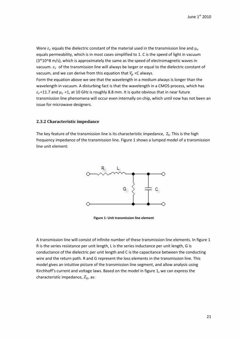
Table 1: List of reflection coefficient with the equivalent RL and SWR
|Γ| (|22|) RL (dB) SWR
0.00 ∞ 1.00
0.05 26.0 1.11
0.10 20.0 1.22
0.20 14.0 1.50
0.30 10.5 1.86
0.40 8.0 2.33
0.50 6.0 3.00
In UWB LNA design we need a broadband matching. Achieving a good match over a wide
frequency range is extremely difficult due to non-ideal and frequency dependent behavior of the
circuit components. All the matching in this thesis has been done on chip, with a very limited
number of reactive components. This complicates the matching, and lowers the achievable goals
somewhat.
2.3.4 The Smith chart
The Smith chart is a useful tool when designing microwave amplifier. It is basically a normalized
reflection coefficient displayer. The Smith chart can be studied in detail in [Ludw 09], and we will
only scratch the surface here. A Smith Chart is shown figure 2:

June 1st 2010
25
Figure 2: Smith Chart, from [Ludw 09]
This Smith Chart is of the combined impedance and admittance type, there also exists an
admittance version and an impedance version. The impedance chart (the circles and arcs
starting from the right) has the normalized real part of the impedance over the horizontal axis,
and the reactive part over the arcs bending upward and downwards (inductive upwards and
capacitive downwards). The Smith Chart is a powerful tool giving an intuitive graphical display of
impedances. This eases the impedance matching process since we can go along reactance arcs
and resistance circles instead of long calculations.
The Smith Chart has one major weakness. This is that it is only valid for one frequency at the
time. That is, the display of the frequency dependant part is not valid if the frequency varies. In
narrow band applications this is often good enough, but in UWB applications we have to do
Smith Charts calculations for more frequencies. Measuring equipment and computer aided
design tools can show how the match varies over frequency in the Smith Chart, but if we are to
do it manually over a wide range of frequencies we need to do many separate computations.
CMOS Microwave LNA design
26
2.3.5 Scattering parameters
Two-port analyses are known to most electronic designers. This way of modeling complex
circuits, by the way it behaves, has been popular since the early age of electronic design. Two-
port analyze is basically a method which handle circuit elements, components or systems as
black boxes, and characterize them by their behavior when they are stimulated a particular way.
Regular two port analysis, like Z-parameters, characterizes black boxes by shorten or opened the
ports and adding signal to the ports. The different values are read out, and we specify the circuit
based by these values.
Earlier in this chapter impedance matching and reflections were described. This is also valid for
two-port analyses of high frequency components or circuits. We need impedance matched two
port analyses. This analysis is called scattering parameter, or just S-parameters.
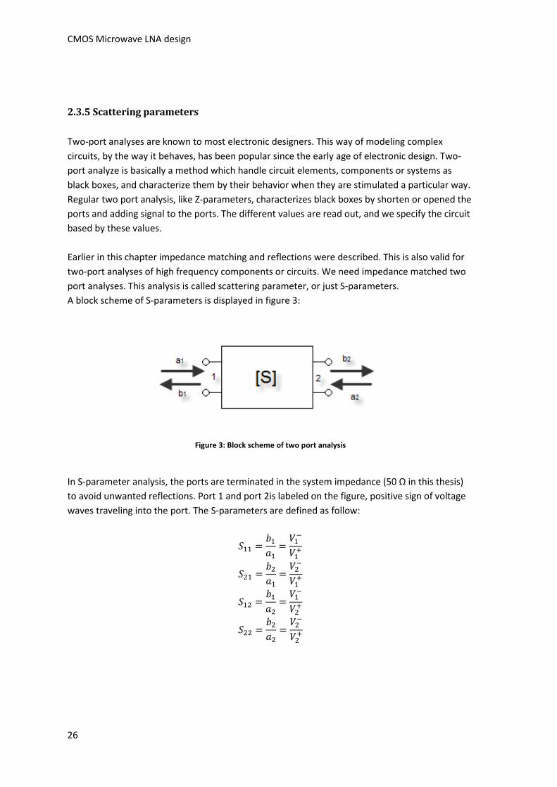
A block scheme of S-parameters is displayed in figure 3:
Figure 3: Block scheme of two port analysis
In S-parameter analysis, the ports are terminated in the system impedance (50 Ω in this thesis)
to avoid unwanted reflections. Port 1 and port 2is labeled on the figure, positive sign of voltage
waves traveling into the port. The S-parameters are defined as follow:
22 = 92:2 = 202#
2 = 9:2 = 02#
2 = 92: = 20#
= 9: = 0#

June 1st 2010
27
S11 and S21 require that port 2 is terminated in the system impedance, while port 1 is stimulated.
S12 and S22 require that port 1 is terminated in the system impedance, while port 2 is stimulated.
The voltages in the equations are high frequencies voltage waves. The sign of the exponent of
the voltage waves indicates the direction of the voltages wave. On the basis the equations we
can describe the different S-parameters as:
- S11 is the input voltage reflection coefficient.
- S21 is the forward voltage gain.
- S12 is the reverse voltage gain.
- S22 is the output voltage reflection coefficient.
If S11 or S22 has a value of 0 dB, the entire voltage wave inserted at the port is reflected back. We
want the values of these two parameters to be as low as possible. A typical value in UWB LNAs is
matching parameters of -10 dB over the entire bandwidth.
S21 is the voltage gain, with we want to be as high possible when designing microwave LNAs. S12
is the backwards isolation, and is thus preferable to have as low as possible
2.4 Input impedance matching techniques
When designing microwave circuits on-chip, we need to match the input and output to the
characteristic impedance of the system. These two terminals interface the chip with the PCB and
to avoid reflections and maintain signal integrity, impedance matching is required.
There are many different matching approaches, often are the methods we find in theory books
meant for off-chip PCB matching. On-chip matching is a bit different since the components we
use often have reduced performance. But the principles are much the same.
Classical matching networks, like t-, π- and similar networks, need many components and are
not relevant in this thesis, due to the large area used by the number of inductors required in
such a network. If the reader wants to read about these types of networks I recommend the
theory book [Ludw 09].
Two generic solutions of input impedance matching using resistors are shown in figure 4. These
two impedance matching solution illustrate basic impedance matching, and do not apply
reactive components. But they still achieve impedance matches up to microwave area (above
0.3 GHz).
CMOS Microwave LNA design
28
Figure 4: Generic wideband impedance matching solutions. A: Resistor terminated common-source. B: Shunt
feedback common-source.
Circuit A, uses resistor RT in parallel with the input as input match. By setting this impedance to
50 Ω, we will achieve a fairly good match. The input match does not affect the gain in the circuit,
which is determined by –gmRL. This means that we can increase the transconductanse of the
amplifier structure without affecting the input match. This is a very simple way to match, but is
widespread in published literature.
Circuit B, uses resistive feedback, Rf, to obtain the match. The expression for the match is in this
case and given by:
;< = + & ∥ >?1 + @(& ∥ >?)
Where Rds is drain-source resistance in the transistor. The feedback resistor, RL, is coupled
between the input and output and therefore affects both the input match and the gain, which is
given by:
AB = − @ − 1 D1 &D + 1 D
This circuit can provide good matching in up to microwave frequencies, and can be extended by
stacking a PMOS on top of the NMOS, making an inverter. An inverter solution would increase
the gain by adding gm of the PMOS.

June 1st 2010
29
When the frequency increases and the band widened, e.g. 1-10 GHz, different matching
techniques are required, and the need for inductors emerges. In this thesis we will strive to
achieve match with the use of as few inductors as possible. The reason for reducing the number
of inductors in the input match is that we need inductors other places in the amplifier to
enhance the bandwidth. In the figure below two high frequency wideband, input match
approaches are displayed. Both these two amplifiers will be analyzed in detail in the next
chapter, so they will only be displayed here for illustration purposes.
Figure 5: High frequency, wide band matching approaches. A: inductor degenerated common source. B: Common-
gate
Circuit A, the source degenerated common-source, is probably the most popular approach for
wideband matching. Circuit B, the common-gate, is not as widespread as B, but the circuit
achieves good broadband matching using few inductors.
2.5 Noise factor and noise figure
Noise figure (NF) is a measure of the noise performance of the circuit, and is derived from the
noise factor (F) of the circuit, [Motc 93]. The noise factor given by the equation below:
E ≡ ;< GHI
This definition shows that F is the factor by which the amplifier degrades the signal-to-noise
ratio of the input signal, and is therefore never smaller than unity. The noise figure is the noise
factor given in dB:

CMOS Microwave LNA design
30
E = 10(E) = 10 K ;< GHIL = ;<,>M − GHI,>M
The noise figure is the difference in dB between the output noise of the actual circuit and an
ideal noiseless circuit. Noise figure and noise factor the two most common parameters to specify
the noise performance of a microwave circuit.
2.6 Bond wire and pad characterization
A big challenge in high frequency design on chip is the influence of the bond wires and the pad,
connecting the pin of the package to the circuit on-chip. This bond wire is inductive coupled to
the neighbor bond wires. The pad on the chip has parasitic capacitance to ground (substrate).
These parasitics are in the microwave signal patch, and are of significant value compared to the
inductors and capacitors included in input- and output impedance matching networks. Ideally
we would want to match the pin of the package to the characteristic impedance of the system,
and not just the circuit on-chip after the pad. The ideal solution is to include the bond wire and
pad in the input matching network and possibly use them constructively. By doing so we could
possibly save one inductor in the input matching, which is a preferable feature. To be able to
include the bond wire and pad in our design phase we need a good model for these two
elements. To make this model we need empirical results, this we achieve by adding test benches
on chip and characterize the behavior by two port analyses or scattering parameters. This bond
wire and pad model will only be valid for the selected package, due to variations in bonding wire
length with different packages. But there is expected that the measurement will to some degree
correlate between the packages.
The package used in this thesis is Quad Flat No leads (QFN) air cavity, which is believed to be the
package of choice for high frequency designs. Air cavity means that the empty space in the
package is not filled up with any material. There were used two different package sizes, in the
chips submitted, one of 48 pins and one of 64 pins. On each chip there were implemented two
test benches. These test benches consisted of bonded pads that were shorted to ground, and
bonded pads that were not terminated at all (i.e. open circuit).
The impedance of the bonding wires can be calculated using W.C Johnson Formula [ John 63] .
The formula is given as:
= N? ∗ G
June 1st 2010
31
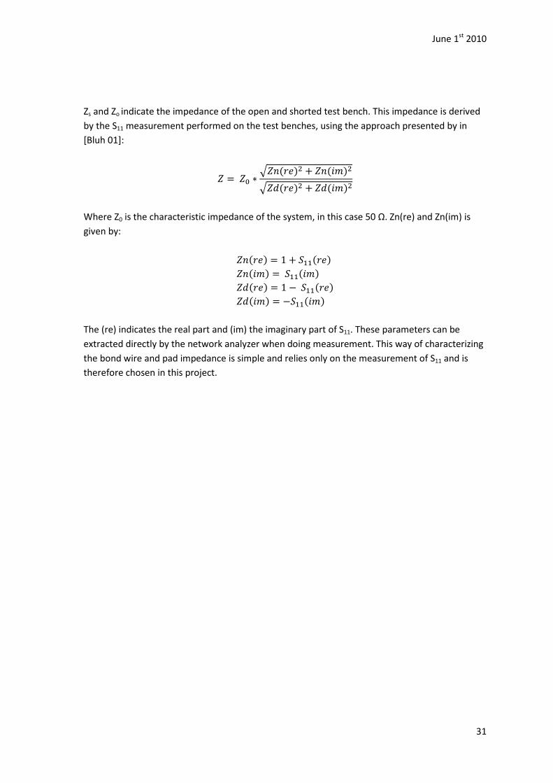
Zs and Zo indicate the impedance of the open and shorted test bench. This impedance is derived
by the S11 measurement performed on the test benches, using the approach presented by in
[Bluh 01]:
= ∗ NO(PQ) + O(R@)NS(PQ) + S(R@)
Where Z0 is the characteristic impedance of the system, in this case 50 Ω. Zn(re) and Zn(im) is
given by:
O(PQ) = 1 + 22(PQ) O(R@) = 22(R@) S(PQ) = 1 − 22(PQ) S(R@) = −22(R@)
The (re) indicates the real part and (im) the imaginary part of S11. These parameters can be
extracted directly by the network analyzer when doing measurement. This way of characterizing
the bond wire and pad impedance is simple and relies only on the measurement of S11 and is
therefore chosen in this project.

CMOS Microwave LNA design
32

June 1st 2010
33
3 Evaluation of the architectures
3.1 Chapter overview
This chapter will present popular UWB LNAs architectures from the literature, and explain some
of the challenges we run into while designing UWB circuits in advanced CMOS processes.
3.2 LNA design strategies
The overall goal of this thesis is to make a low power prototype UWB LNA with bandwidth from
1-10GHz in 90 nm CMOS technology. The secondary goal is to minimize the number of inductors
needed to achieve the overall goal. There are other processes available, but the motivation for
using CMOS is:
- it is a widespread technology.
- it possesses a good design tool kit.
- the production is relatively cost-effective.
- Small feature size → low power
There are a number of proposed solutions for UWB LNAs in the literature, and in the initial
phase many of these where studied. Based on literature evaluation a few promising topologies
where selected for further modeling and eventually four topologies were implemented using
silicon in 90 nm technology.
3.2.1 Process challenges
The TSMC 90nm process used is a low power process with supply voltage of 1.2 V which is 0.2V
higher than the general purpose process from the same vendor. Low power process means that
it has thicker gate-dioxide, which leads to lower leakage current. This process is somewhat
slower than the general purpose process, reducing performance somewhat. At the highest
frequencies we enter the transition band of the amplifier topologies, making it a necessity to
include bandwidth enhancers to obtain the specified bandwidth. CMOS is primarily a digital
technology, and in digital design the low supply voltage is not a disadvantage. When doing
analog design, however, the reduced supply voltage introduces new design challenges. We are
no longer able to stack as many devices and it also degrades the Signal-to-Noise Ratio (SNR) –
CMOS Microwave LNA design
34
since the SNR is proportional to the square of the supply voltage. This limits the number of
architectures that is practical to use. Architectures stealing headroom, i.e. stacking many devices
between the rails are not desirable. Willy Sansen has some interesting thought on this issue, see
[Sans 05], where he concludes that technologies smaller than 180 nm CMOS is not suitable for
analog or high frequency applications. There are other production processes more optimized for
analog and high frequency design, like Bi-CMOS, Silicon-Germanium (SiGe) or Gallium Arsenide
(GaAs) which allows for higher frequencies, higher supply voltage and have better noise
performance at microwave frequencies, but CMOS is most cost-effective.
The bonding wire and the pad are also factors that affect performance when designing UWB
LNAs. Ideally we should have good models for these and include them in our design process.
3.2.2 Bandwidth enhancement techniques
When designing UWB LNAs in the process used we push the amplifier topologies to the limits,
making it necessary to use bandwidth enhancing techniques. With bandwidth enhancers we
mean structures that resonate towards the higher frequencies of the bandwidth and basically
force the gain to stay higher for longer. These bandwidth enhancers usually include at least one
inductor. On-chip inductors are made, in the process used, planar. Because the inductor is made
planar in one metal layer, rather than stacked through the metal layers available, it occupies
large silicon area. We are not allowed to have circuit structures underneath the inductor, since
this would lead to unpredictable behavior in both the inductor and the circuit lying beneath. The
bandwidth enhancement inductors do not necessary have to have a very high Q because we
want the inductor to peak over a wide frequency range rather than a high peaking over a narrow
frequency range, which would be preferable in a narrow band design. The equation for Q factor
in a reactance is:
T = UV"U
Where X equals the reactive part of the reactance and R equals the series resistance. Since the
inductors are made planar, the length of the routing and thereby the size of parasitic series
resistance, increases considerable compared to the size of the inductance. As we can see from
the equation the series resistance will decrease the Q –factor of the inductor. Low Q means
smaller peaking over a wider frequency range in this context, and can be an advantage when
designing UWB LNAs. The drawback of the low Q factor is clearly that the peaking effect is
limited.

June 1st 2010
35
There exist a number of bandwidth enhancement techniques, but in order to minimize the
number of inductors used, only a few generic methods requiring a small amount of inductors will
be presented here.
3.2.2.1 Series peaking enhancement
A classical bandwidth enhancement technique is the series peaking, shown in a resistor loaded
common source stage in figure 6. The capacitance on in the figure is a lumped representation of
the parasitic load capacitance.
Figure 6: Series peaked common source amplifier
The series peaking bandwidth enhancement technique is one of the oldest bandwidth
enhancers, and the idea is that the inductor counteract the effect of the capacitor within a
limited band. With some mathematics, [2LEE 04], we may extend the bandwidth √2 times in
theory. This bandwidth boost comes entirely form the introduction of a new complex pole pair
when the series inductor is added. Without this series inductor is the bandwidth limited to the
RC time constant of the load resistor and the parasitic capacitor. This bandwidth extension
technique is quite effective, but the resistive load limits the headroom. This is not desirable at
low supply voltage. In addition we can achieve more bandwidth enhancement by connecting the
inductor differently, e.g. shunt peaking.

CMOS Microwave LNA design
36
3.2.2.2 Shunt peaking enhancement
By connecting the inductor in series with the load resistance, as is shown in figure 7, we achieve
better performance than with the series peaking. The circuit is a standard common source
topology with an inductor in series with the resistor. It is called shunt peak since this inductor
appears in series with the resistor and in parallel with the load capacitance in a small signal
equivalent.
Figure 7: Shunt-peaked common source amplifier
The capacitor here represents the lumped parasitic capacitance or the load capacitance with
decreasing impedance for increasing frequency. The inductor has increasing impedance with
increasing frequency, i.e. it introduces a zero in the transfer function. This helps offset the
decreasing impedance introduced by the capacitance, leaving the net impedance more or less
constant over a wider frequency range. The simplified gain in a circuit like this is given by @&
where & is the combined impedance of the resistor, inductor and the capacitor. By this
technique we can theoretically increase the bandwidth 1.85 times, see [1Lee 04] and [2Lee 04].
This would introduce a peak in the pass band of the amplifier though, but gives an idea of the
potential of simple bandwidth enhancers.
Peaking inductors are fundamental bandwidth enhancement techniques, and are good examples
of what we are aiming for. We want a non-impedance-stable load to compensate for the gain
loss introduced by capacitive parasitics. These two frequency responses should compensate for
each other and form a frequency response with a flat gain over a wider frequency range. In a
June 1st 2010
37
modern process with low supply voltage, a pure inductive load would be an alternative to the
combined resistive and inductive load shown in figure 7. The lower Q factor of on chip inductors
is actually an advantage and reduces the need for series resistor.
There are many bandwidth enhancers that use both series peaking and shunt peaking
techniques. These will not be explained here, se [1Lee 04] and [2Lee 04].
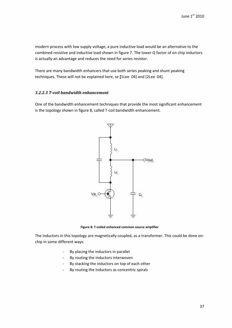
3.2.2.3 T-coil bandwidth enhancement
One of the bandwidth enhancement techniques that provide the most significant enhancement
is the topology shown in figure 8, called T-coil bandwidth enhancement.
Figure 8: T-coiled enhanced common source amplifier
The inductors in this topology are magnetically coupled, as a transformer. This could be done on-
chip in some different ways:
- By placing the inductors in parallel
- By routing the inductors interwoven
- By stacking the inductors on top of each other
- By routing the inductors as concentric spirals

CMOS Microwave LNA design
38
These methods require the use of custom made inductors. This would require extensive
simulating and modulating and should also be verified through measurements, which is time
consuming. But by connecting the inductors like the T-coiled common source amplifier we can
theoretically enhance the bandwidth with as much as 2.83 times, which may justify the efforts of
custom inductor design.
Since low Q-factors in inductors actually may be an advantage in UWB design, it is interesting to
explore the possibility of customized inductors by winding through the metal layers available in
the process and thereby saving area on chip. This opens a wide specter of feasible amplifier
structures which can be optimized for UWB.
3.3 UWB LNA architectures
When designing UWB LNAs there are several different approaches we can use, this section will
present some generic design approaches and some design samples from the literature.
3.3.1 Generic architectures
This project started with a literature study on UWB LNAs. This study showed that some generic
architectures frequently emerged. These architectures were:
- Source degenerated common source amplifiers
- Cascoded common gate amplifiers
- Cascaded amplifiers (aggregated amplifiers)
In this section we will explain the basics of these generic architectures.
3.3.1.1 The common source amplifier
Different versions of source degenerated common source amplifiers are widespread throughout
the literature. Common source amplifiers are popular due to their simplicity and the relatively
large gain. An example of a source degenerated common source amplifier is shown in figure 9:

June 1st 2010
39
Figure 9: Common source amplifier
The degeneration inductor is connected between the source and ground. By doing this we
achieve an improved input match. This is more intuitive to see when we see the small signal
equivalent of an inductor generated transistor:
Figure 10: Small signal equivalent of a source degenerated transistor1
In the small signal equivalent the parasitic capacitor between gate and drain is left out for
simplicity. If we forget the inductor for a moment, we see that the gate-source capacitance, Cgs ,
will cause an impedance drop at the input for high frequencies. The impedance drop will
degrade the S11 , which leads to decreased gain and possible reflections. To compensate for this
decreased input impedance, the source degenerated inductor is connected between source and
ground to maintain the required impedance at high frequencies. This not only improves the S11 ,
but also the NF which is a very important property of a LNA. This is a popular basic architecture
1 Picture taken from: http://www.odyseus.nildram.co.uk/RFIC_Circuits_Files/MOS_CS_LNA.pdf

CMOS Microwave LNA design
40
for many UWB LNAs, and is a good starting point which can be expanded with cascaded
topologies for increased gain.
3.3.1.2 The common gate amplifier
The common gate amplifier is a popular input stage in UWB LNAs, due to the common gate
amplifiers input matching properties. A common gate amplifier is showed in figure 11:
Figure 11: Common gate amplifier
In a common gate amplifier the input is connected to the source of the transistor while the gate
is held at a stable voltage. In figure 11 an inductor is coupled between the input/source of the
transistor to ground. This inductor improves the input match of the amplifier and enhances the
bandwidth. It is easier to see this if we take a look at the small signal model of a transistor
without the inductor at the source, as shown in figure 12:

June 1st 2010
41
Figure 12: Small signal equivalent2
In common source topology the small signal gate terminal is grounded and the input is source
connected. Seen from the source we see that the drain-source capacitance ,Cds , will reduce the
input impedance at high frequencies. This degrades the S11 , which leads to undesirable effects.
To compensate for this impedance drop, we introduce an inductor at the source terminal. This
inductor compensates for the impedance drop introduced by Cds, making the drain source
resistance ,Rds, dominating over the bandwidth. Rds is approximately equal to 1/gm, making the
input match dominated by the transistor biasing. This is very practical and the common gate
amplifier is therefore popular in the UWB LNA literature. We achieve a good broadband
impedance match, using few components. This makes the common gate topology a popular
input stage in cascaded amplifiers. The drawback of a common gate configureation is non ideal
noise due to its low gain, compared to common source.
3.3.1.3 Aggregated systems: Cascaded amplifiers
Aggregated systems in the form of cascaded topologies are common in UWB amplifier design.
The principle of cascaded amplifiers is to achieve a higher gain by coupling gain stages in series,
called cascade coupling. The gain stages can be of any type, but common choices are common
source, common gate and inverter stages.
2 Picture taken from: http://www.odyseus.nildram.co.uk/RFIC_Circuits_Files/MOS_CS_LNA.pdf

CMOS Microwave LNA design
42
Figure 13: Cascaded amplifier stages
Figure 13 show a cascaded amplifier, the total gain of a amplifier of this type is given by:
AIGIXY = A2 ∗ A ∗ AZ
Where the subscript indicates the number of the gain stage. From the equation we see the large
increase in gain cascading represents, the total gain is given by the product of the gain of the
individual stages. The tradeoff in cascaded amplifiers of this type is that the bandwidth, ω0, is
reduced. This bandwidth reduction is given by the equation below. N indicates the number of
stages.
[G< = [ N22 <D − 1
To achieve good noise properties in a cascaded amplifier it is important to have large gain and
low noise in the first gain stage. If we take a look at Friis formula for noise in a system we see:
EIGIXY = E2 + \]02'^ + \_02
'^'] + \ 02'^']'_ + ⋯
Here F is the noise factor of the gain stage, G is the gain of the gain stage and the subscript
indicates which number in the cascaded chain the gain stage possesses. If the gain in the first
stage is sufficient, F1 will dominate the noise performance.
There exist cascaded topologies that do not have the same bandwidth for gain tradeoff, but
rather delay for gain tradeoff. This is a much more preferable tradeoff in most UWB systems.
These cascaded amplifiers are called distributed amplifiers.

June 1st 2010
43
3.3.1.4 Cascaded amplifiers: The distributed amplifier
An elegant and interesting design technique is the distributed amplifier. This is a version of
cascaded amplifiers that actually achieves better gain bandwidth product (GBW) than each
individual stage without reducing the bandwidth. The concept is illustrated in figure 14 where
each gain stage is illustrated by a common source transistor. This gain stage can in principle be
any gain stage.
Figure 14: Distributed amplifier, from [Haji 03]
The concept of distributed amplifiers is to introduce separate delay lines on the input and
output, and explore the wave propagation in these delay lines to enhance the bandwidth and
the gain. These delay lines are made as transmission lines, made up by inductors and the
parasitic capacitances on the input and output of each gain stage, i.e. we absorb the parasitic
capacitance of each stage. A signal applied to the input propagates down the delay line, causing
the signal to appear at the input of each gain stage in succession. Each gain stage responds to
the signal at the input by generating a current at the output equal to its transconductance, gm,
times the magnitude of the input signal. If the delay lines of the input and output lines are
matched, the currents from all the gain stages sum up at the output (KCL). The generic
expression for gain in a distributed is given by:
Ab = O ∗ @ ∗ -1
Where n is the number of stages, gm is the transconductance of each stage and Z0 is the
characteristic impedance of the transmissions lines between the stages making up the delay line.
Each transmission line segment at the output line is loaded twice presenting the impedance of -1 . From the expression we see the gain is linearly dependent on the number of gain stages. This
means that we can use this technique at frequencies where the gain in each stage is less than

CMOS Microwave LNA design
44
unity, i.e. over the unity gain frequency of each stage. As a consequence we can operate
distributed amplifiers at much higher frequencies than conventional amplifiers, making this a
generic technique we can always use if all other alternatives fail. To achieve the desired gain we
just add gain stages, until we reach our target. The cost is more area, and complex simulations.
3.3.2 Explored architectures
This section will explore the most promising published architectures from each generic
architecture found in the literature evaluation.
3.3.2.1 Source degenerated common source amplifier
This source degenerated common source amplifier, is shown in figure 15, were first published by
Andrea Bevilacqua and Ali M. Niknejad, [Bevi 04].
Figure 15: Source degenerated common source amplifier, [Bevi 04]

June 1st 2010
45
Here we have an extensive input matching network of Chebyshev type. This network includes a
bias voltage node, which sets the bias point for the common source transistor. The Ls inductor
purpose is to degenerate the transistor for improved input match. The match is improved since
this inductor cancel out some of the impedance drop at high frequencies, caused by the gate-
source capacitance of the transistor. The cascaded common gate transistor is inserted for some
additional gain but more important to create a stabile load for the common source and to
increase the output impedance seen from the output, i.e. improve the output match c. The
gain of this circuit is given by:
Ab = bdefbgh = − ijk(?)
?f"l ∗ "/K2#l//m/ L2#?"/def#?]&/def
Where &is the load resistance of the circuit, and n& is the load inductance. GHI corresponds to
the capacitance between the drain of the common gate, M2, and ground (drain-bulk capacitance
of M2, and the gate-drain capacitance of the buffer, M3 and M4), I equals the input capacitance
of the common source (the and the gate-source capacitance), W(s) is the transfer function of
the input Chebychev filter. The load uses inductive peaking as a bandwidth enhancer. As we can
see from the expression the gain roll-off is compensated by n& in the numerator in the second
fraction. The n& inductor peaks as the frequency rises, providing an increased load which again
provides an increased gain. If this peaking is optimally connected we maintain gain where the
amplifier itself enters the transition band. We also need to keep the resonance introduced by
cn&GHI out-of-band, which could otherwise cause oscillations. The output current buffer is
added for measuring purposes, this increases the current driving capabilities, but also increases
GHI contributing to gain roll-off at higher frequencies.
The performance of this amplifier implemented in a 0.18µm CMOS process is presented in table
3.1:
Table 2: Performance of source degenerated common source amplifier
S11 [dB] BW [GHz] Gain [dB] NF [dB] Pdiss [mW]
<-9.9 2.3-9.2 9.3 4-10 9
This amplifier is a quite simple and intuitive amplifier topology, based on classical common-
source common-gate architecture. It achieves good matching properties, low power
consumption and almost the target bandwidth of this thesis. The drawbacks are extensive
matching network and many inductors, which again makes this LNA area hungry. The gain is not

CMOS Microwave LNA design
46
as high as desired when we take into account the number of inductors used. But the main
drawback of this architecture is the noise performance, this vary too much over the bandwidth
and is somewhat shaped. The size of this architecture, its moderate gain and its NF was the main
reasons this architecture was not considered further.
3.3.2.2 Common gate amplifier with interstage matching network
The next architecture explored is an architecture presented by Stanley Bo-Tang in his PhD thesis,
[Stan 05]. This architecture uses a common gate input stage and an interstage network between
the input common gate stage and the cascoded common gate stage. The architecture is shown
below:
Figure 16: Common gate amplifier with interstage matching network [Stan 05]
The input common gate stage is biased for high gain, this reduce the input impedance, looking in
to the source of the input transistor. The input impedance of the transistor is approximately
given by 1/gm. To compensate for this low input impedance a quite extensive input matching

June 1st 2010
47
network is added. The inductor which is connected between the source of the input transistor
and ground is for source degeneration, i.e. compensating for the source-drain capacitance at
high frequencies. The interstage network consists of two inductors and one capacitor. The
purpose of this interstage network is to optimize the impedance between the two common gate
stages. The load does not provide flat impedance, and therefore it is necessary to boost the gain
at some frequencies. The interstage network acts as an impedance transformer. The impedance
seen by the lower stage is much higher than the impedance seen by the upper stage. This gives a
current boost which gives additional gain, and is exploited by Stanley Bo-Tang in [Stan 05] to
achieve increased gain linearity over the entire bandwidth. The buffer at the output is added for
measuring reasons. If we assume perfect match at the input and a lossless interstage network,
the gain is given by the expression:
Ab = defl = -/(%)
"l !ij^"lo ! ij]d^
2#-/(%)/1]
Here ? is the ideal source resistance, which in most cases is 50 Ω, @2 is the transconductance
of the first stage, @ is the transconductance of the second, PG2 is the impedance looking into
the drain of stage 1, PG is the impedance looking into the source of stage 2, &([) is the load
impedance.
The performance of this amplifier implemented in a 0.13 µm process is presented in table 3:
Table 3: Performance of common gate amplifier with interstage matching network
S11 [dB] BW [GHz] Gain [dB] NF [dB] Pdiss [mW]
<-10 2.95-8.6 12.4 4-6 14.4
This amplifier achieves good gain, good matching properties, good NF and acceptable power
consumption. The tradeoffs are the somewhat limited bandwidth and the area it occupy due to
complexity of the input matching network and the interstage matching network. The interstage
network need inductive coupled inductors. This means that in order to realize the interstage
network, we have to modulate our own inductors which is time consuming and difficult. The
large number of inductors was the reason for dropping this topology from further evaluation.
But the idea of using a common gate input is interesting, and with smaller and coupled inductor
models this would be an interesting architecture take further.
CMOS Microwave LNA design
48
3.3.2.3 Distributed amplifier with telescopic cascode common source common gain
stages
This version of the distributed amplifier architecture was published by P. Heydari in [Heyd 07].
Heydari uses gain stages consisting of telescopic cascoded common source common gate stages,
and he makes artificial transmission lines using inductors and the parasitic capacitance in the
gain stages. The circuit is shown in figure 17:
Figure 17: Distributed amplifier. From [Heyd 07], copyright © 2007 IEEE
The output delay line is connected to the drain of the cascaded common gate transistors, while
the input delay line is connected to the gate of the common source transistors (for generic
description of these delay lines, see section 3.3.1.4). These delay lines are formed as
transmission lines by the inductors and the parasitic capacitance of the gain stages, which means
we balance the capacitances. The inductor between the CS and the CG, in the gain stages, works
as an interstage network, which absorb the parasitic capacitance to ground in the node between
the CG and the CG. By doing this we move the pole in this node higher up in frequency, and
thereby increase the bandwidth. The artificial transmission lines works as delay elements which
sum up the current gain of each of the gain stages at the output. The gain is dependent on the
number of stages and we can thereby increase the gain by simply adding more stages, the
tradeoff with this is that we need more inductors.
The performance of this architecture implemented in a 0.18 µm SiGe process is displayed in
table 4:

June 1st 2010
49
Table 4: Performance of distributed amplifier with telescopic cascode common source common gain stages
S11 [dB] BW [GHz] Gain [dB] NF [dB] Pdiss [mW]
<-12 0.1-11 8 2.9 flat 21.6
This architecture achieves very good broadband matching, more than enough bandwidth and
superb NF. Drawbacks are not as much gain, but this can be increased by adding more stages.
But the main problem with this architecture is the number of inductors required, and thereby
the area it occupies. We need three inductors per stage and four on the input and output
combined. This would be a very large architecture if realized in the process used. If we can
decrease the size of the inductors dramatically, by modulating them ourselves, this architecture
would be extremely interesting. The noise performance of this amplifier is superb, and we can
achieve high bandwidth as long as we add the number of gain stages required, the same goes for
the gain. Nevertheless is this a design approach we can fall back to if all other approaches fail.
3.3.2.4 Inverter based amplifier using splitting-load inductive peaking technique
The next architecture uses an interesting technique which the authors call Splitting-Load
Inductive peaking. The architecture was first published by S-F. Chao, J-J Kuo, C-L. Lin, M-D- Tsai
and H. Wang in 2008, [Chao 08]. The architecture is based on cascaded shunt feedback inverters.
The circuit is shown below in figure 18.
Figure 18: Inverter based amplifier using splitting-load inductive peaking technique [Chao 08]
The peaking inductors L1 and L2 are included to enhance the bandwidth while L3 is included to
improve the output match S22. Without employing peaking inductors the bandwidth of the
amplifier is determined by the RC time constants of each node. In CMOS processes the load

CMOS Microwave LNA design
50
capacitance of these nodes is quite high, due to the gate and parasitic capacitance of the
transistors. The peaking inductor in this topology is connected to the gate of the NMOS, as
opposed to conventional series peaking inductor [Wu 05]. By connecting the inductors this way,
they are only loaded by the gate capacitance of the NMOS. This push the dominating pole in the
transfer function from q!niri?< + i?st02
to rNnii?<s02 , which enhances the bandwidth
significantly. Simulated single stage inverter performance is shown in the figure below:
Figure 19: Simulated gain performance of single state inverters. From [Chao 08], copyright © 2008 IEEE
As we see from figure 19, it seems the splitting load technique is a much more efficient
bandwidth enhancement than conventional series peaking.
Inverter based amplifiers have many advantages, they are rail-to-rail amplifiers with quite large
gain (gmn+gmp). The gain for one stage in the inverter solution is given by:
Ab = defgh = 2
2#?]&^ulh ∗ 20"v(ij<#ij)#?]ulh&^r20ij"vs2#"vr?wlh#?wl#dx^#dhx^s
We see the dominating pole in the first fraction and the gain boosting effect of inverters in the
nominator of the second fraction. The performance of this architecture implemented in a 0.13
µm CMOS process is displayed in table 5:

June 1st 2010
51
Table 5: Performance of inverter based amplifier using splitting-load inductive peaking technique
S11 [dB] BW [GHz] Gain [dB] NF [dB] Pdiss [mW]
<-8 DC-11.5 13.2 <5.6 9.1
This architecture achieves a very large bandwidth, low power consumption, high gain and
acceptable matching properties. The NF is a bit high, but still not unacceptable. The architecture
is simple and uses an exciting inductor coupling technique to enhance the bandwidth. This
architecture was selected for further investigation.

CMOS Microwave LNA design
52

June 1st 2010
53
4 Circuit implementation
4.1 Chapter overview
Four LNAs has been implemented in 90 nm CMOS. This chapter will present the implemented
circuits, shortly present the pad frame and illustrate layout strategies used when designing the
circuits.
4.2 The architecture chosen and specification goals
The LNAs that ended up on-chip, were all based on the topology presented in [Chao 08]. The
reason for choosing this topology is its simplicity, compactness and promising performance
when produced in a less advanced process. The fact that there was some severe design kit issues
during the design phase also made it convenient to go for only one type of topology. By basing
all implemented circuits on one topology it is easier to show and discuss the tradeoffs between
inductor connections in this specific circuit. Two of the implemented versions used only two gain
stages, for reduced power consumption.
The overall performance goal or specification laid down at the start of this project was:
- Low power consumption (no specific value was set)
- A -3bB bandwidth 1-10 GHz
- Gain, S21 > 8dB (3.1-10.6 GHz)
- S11 < -10dB
- NF < 5dB
During the development of the designs it became clear that achieving a 10 GHz bandwidth
probably was too demanding the process used (TSMC CMN90LP). The low power process has
reduced performance compared to the general purpose process from TSMC, making it even
more challenging meeting specifications. A more realistic specification of 8.5 GHz were adopted
as reasonable, this taken in to account that the unlicensed UWB band in Europe stretches from 6
to 8.5 GHz, not 3.1 to 10.6 in the US. The input match goal and NF goal also turned out to be too
difficult to meet given the additional power limits.
4.3 Implemented LNAs
Three different chips were sent for production, all including at least one LNA. Two of the chips

CMOS Microwave LNA design
54
were prepared for measurement, the master-chip (64 pins) and the test-chip (48 pins), the last
chip was a system chip without measurement possibilities of the front-end. The LNAs were all
matched to 50 Ω input- and output impedances excluding bonding wires and pads. This decision
was made since no bonding wire model was available, and to compensate for something
unknown seemed to make little sense. Instead bond wire test benches, as described in chapter
2, was included for characterization.
The architectures were evaluated through S-parameter analysis, with power gain (S21), matching
properties (S11 and S22), and noise performance (NF), being the dominating parameters. The
design phase was based mainly on layout simulations since there were large deviations between
the schematic simulations and the post layout simulations (PLS). Thus significant resources were
used tuning the layout and simulate for best performance.
4.3.1 LNA architecture 1
The first architecture implemented is the only architecture with three inductors. The schematic
is shown in figure 20. During the exploration of this circuit it became clear that good input
matching was extremely difficult to achieve with few inductors. If the input matching inductor,
L1, was connected in series with both the PMOS and NMOS , rather than the splitting load
technique presented in [Chao 08], better broadband matching occurred. In section 4.3.5 the
performance of the splitting-load approach is compared to the series approach. The improved
matching properties with the conventional series connection of the input inductor L1 was chosen
for this circuit.
Figure 20: Schematic LNA 1
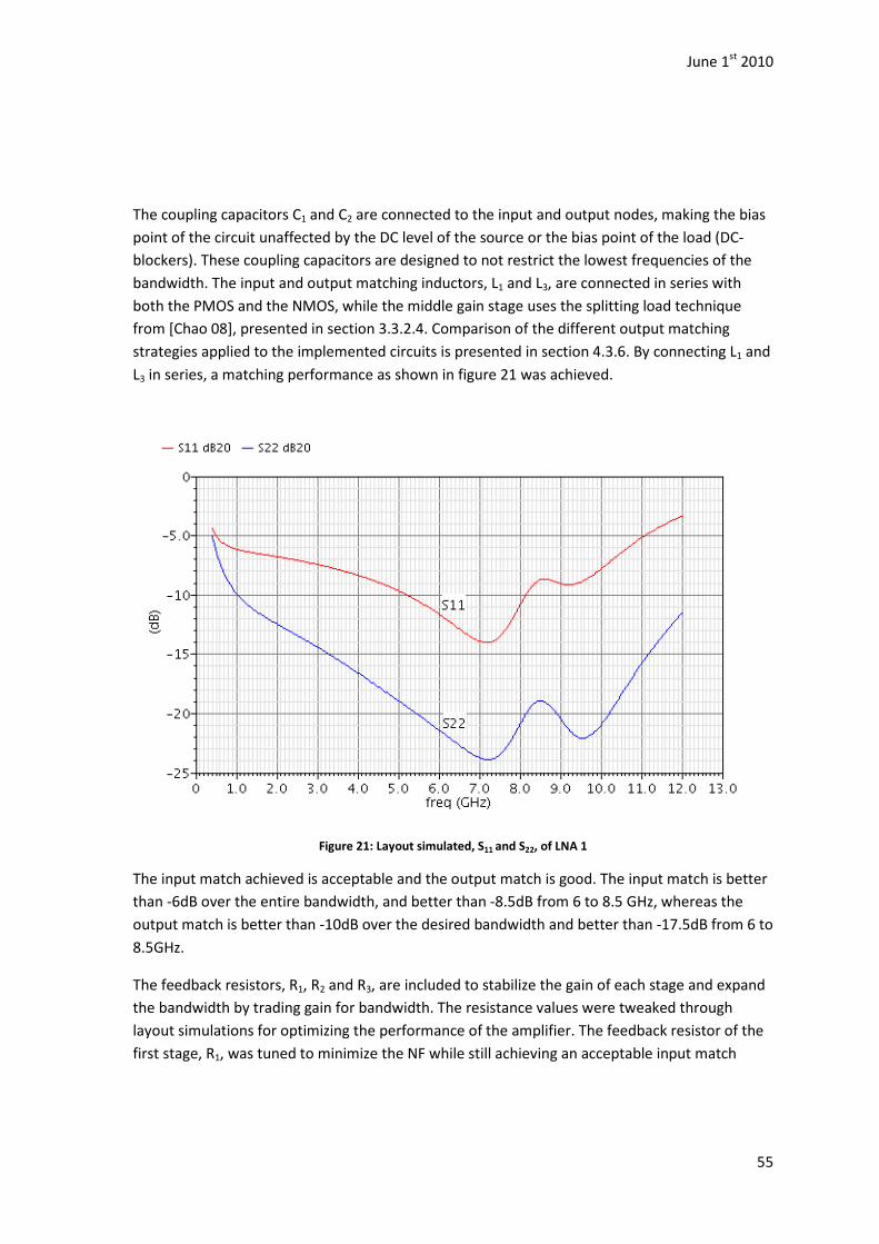
June 1st 2010
55
The coupling capacitors C1 and C2 are connected to the input and output nodes, making the bias
point of the circuit unaffected by the DC level of the source or the bias point of the load (DC-
blockers). These coupling capacitors are designed to not restrict the lowest frequencies of the
bandwidth. The input and output matching inductors, L1 and L3, are connected in series with
both the PMOS and the NMOS, while the middle gain stage uses the splitting load technique
from [Chao 08], presented in section 3.3.2.4. Comparison of the different output matching
strategies applied to the implemented circuits is presented in section 4.3.6. By connecting L1 and
L3 in series, a matching performance as shown in figure 21 was achieved.
Figure 21: Layout simulated, S11 and S22, of LNA 1
The input match achieved is acceptable and the output match is good. The input match is better
than -6dB over the entire bandwidth, and better than -8.5dB from 6 to 8.5 GHz, whereas the
output match is better than -10dB over the desired bandwidth and better than -17.5dB from 6 to
8.5GHz.
The feedback resistors, R1, R2 and R3, are included to stabilize the gain of each stage and expand
the bandwidth by trading gain for bandwidth. The resistance values were tweaked through
layout simulations for optimizing the performance of the amplifier. The feedback resistor of the
first stage, R1, was tuned to minimize the NF while still achieving an acceptable input match
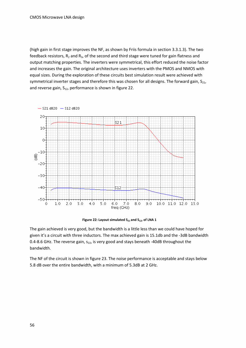
CMOS Microwave LNA design
56
(high gain in first stage improves the NF, as shown by Friis formula in section 3.3.1.3). The two
feedback resistors, R2 and R3, of the second and third stage were tuned for gain flatness and
output matching properties. The inverters were symmetrical, this effort reduced the noise factor
and increases the gain. The original architecture uses inverters with the PMOS and NMOS with
equal sizes. During the exploration of these circuits best simulation result were achieved with
symmetrical inverter stages and therefore this was chosen for all designs. The forward gain, S21,
and reverse gain, S12, performance is shown in figure 22.
Figure 22: Layout simulated S21 and S12, of LNA 1
The gain achieved is very good, but the bandwidth is a little less than we could have hoped for
given it’s a circuit with three inductors. The max achieved gain is 15.1db and the -3dB bandwidth
0.4-8.6 GHz. The reverse gain, s22, is very good and stays beneath -40dB throughout the
bandwidth.
The NF of the circuit is shown in figure 23. The noise performance is acceptable and stays below
5.8 dB over the entire bandwidth, with a minimum of 5.3dB at 2 GHz.

June 1st 2010
57
Figure 23: Layout simulated NF of LNA 1
The NF rises rapidly over 9 GHz, as is also the case for the published results of similar topologies.
To decrease the NF we would have to trade it for input matching and bandwidth, which we
considered to be more important in this design.
4.3.2 LNA architecture 2
LNA 2, see figure 24, is a two stage circuit. It uses the first and last stage from [Chao 08], but with
symmetrical inverters. The first stage provide both input match and peaking. The peaking
inductor L1 moves the dominant RC pole from the input node up in frequency and thereby
enhances the bandwidth (as already discussed, [Chao 08] claims this gives better performance
than series peaking solutions as presented in [Wu 05]). By using an input stage of this kind, we
do not achieve as good input matching as with conventional series inductor. The solution is
chosen since it, together with LNA 3, gives good data about inductor connection tradeoffs in this
circuit. The circuit is shown in figure 24.

CMOS Microwave LNA design
58
Figure 24: Schematic LNA 2
This version uses an inductor at the drain of the NMOS of the last stage, this makes it possible to
increase the gain of the last stage without degrading the output match. This gives better output
matching properties than the solution proposed in LNA3 (see next section). The input and output
match is shown in figure 25 as a function of frequency:
Figure 25: Post-layout simulated S11 and S22, of LNA 2

June 1st 2010
59
The input match has an almost narrowband frequency response, with a large dip between 8 GHz
and 9.2 GHz. This can indicate that the Q-factor of the inductor used in the input match could be
reduced to widen the match. The input match is not good, and it achieves a S11 of less than -3dB
over the entire bandwidth, and less than -4.5 from 6 to 8.5 GHz. The output match looks better
and is below -6.5dB over the entire bandwidth and lower than -8.8dB from 6 to 8.5 GHz. The
matching properties are therefore not as good as with series matching applied in LNA 1.
Since this circuit only includes two gain stages we achieve a lower gain than in the three stage
versions. The S21 and S12 for LNA 2 are plotted in figure 26.
Figure 26: Post-layout simulated S21 and S12, of LNA 2
The gain is higher at the lowest frequencies of the bandwidth. The topologies all have a large
gain from 1 GHz to about 4 GHz, which has been minimized in all of the designs by tuning C1 and
R1. It seems like proposed topologies are very comfortable in this frequency band and boosts the
gain here. The ripple in the pass band of this circuit is 4 dB, making the gain 10.4±2.5 dB from 0.4-9
GHz. The reverse gain, S12, maintains a value of less than – 31dB over the entire bandwidth. A
ripple of this size will be too large for many applications but this solution was still implemented
since it together with LNA 3, gives an insight in the tradeoffs using inductors in this topology.
The noise performance of this circuit is displayed in figure 27, and is almost as good as LNA 1,
even with gain and input match significantly reduced.

CMOS Microwave LNA design
60
Figure 27: Post-layout simulated NF of LNA 2
The NF stays below 6dB over the entire bandwidth, with a minimum of 5dB at 8.2 GHz. This is
acceptable given that there are only used two inductors.
4.3.3 LNA architecture 3
LNA 3 is a two stage version of [Chao 08] topology. It utilizes two peaking gain stages, applying
the splitting load technique.

June 1st 2010
61
Figure 28: Schematic LNA 3
The input match is handled by a stage identical to that of LNA 2, but the output stage is
different. There is no inductor at the output of the last stage, instead the match is obtained by
tweaking the transistor sizes and feedback of the last stage. By this method a promising output
match was obtained in schematic simulations, which seemed to almost eliminate the need for an
inductor at the output. This output match was degraded in layout as shown in figure 29.
Figure 29: Post-layout versus schematic S22 simulations of LNA 3

CMOS Microwave LNA design
62
The schematic version, plotted in red, provides acceptable output matching properties over the
entire bandwidth (<8dB), the degradation is caused by the layout. In figure 30 is the schematic
and layout output impedances plotted in a Smith Chart:
Figure 30: Post-layout versus schematic S22 simulations of LNA 3
In the Smith Chart, the layout simulations is plotted in blue and schematic simulations in red,
both have been marked with a marker at 8.5 GHz. As we see the layout simulations are more
capacitive and low resistant at the 8.5 GHz point, making the impedance mismatch worse. This
layout degradation is not caused by the layout extraction of the transistor models, since the RF
transistors used include all parasitics in the schematic model (section 4.5.2.3). This indicates that
the routing or other components are the cause for this degradation. After submitting the chip I
have done some evaluation, finding that the routing most likely is the reason, this is because the
node between the last gain stage and C2 was routed with wide lines in metal 1. Metal 1 is closest
to the substrate making the capacitance between the routing and substrate relatively large. The
signal routing should have been routed in the top metal layers (metal 7 to 9) since these are
thicker, giving less parasitic resistance in the routing, in addition to the reduced capacitance to
substrate. Routing in the thickest metal layer, farthest from the substrate is in general good
design practice in high frequency circuits.
The input and output match simulation for this circuit is shown in figure 31.
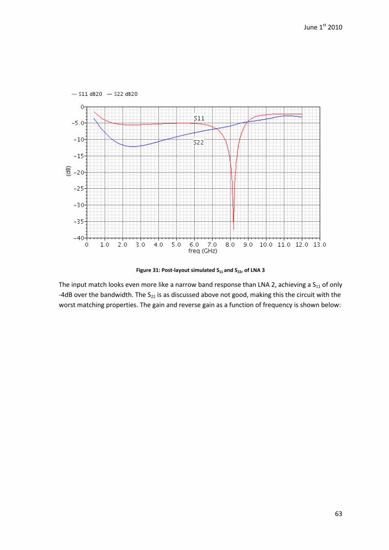
June 1st 2010
63
Figure 31: Post-layout simulated S11 and S22, of LNA 3
The input match looks even more like a narrow band response than LNA 2, achieving a S11 of only
-4dB over the bandwidth. The S22 is as discussed above not good, making this the circuit with the
worst matching properties. The gain and reverse gain as a function of frequency is shown below:
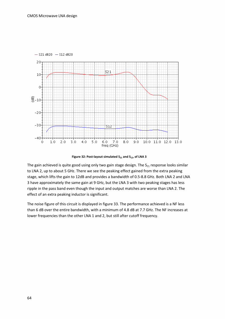
CMOS Microwave LNA design
64
Figure 32: Post-layout simulated S21 and S12, of LNA 3
The gain achieved is quite good using only two gain stage design. The S21 response looks similar
to LNA 2, up to about 5 GHz. There we see the peaking effect gained from the extra peaking
stage, which lifts the gain to 12dB and provides a bandwidth of 0.5-8.8 GHz. Both LNA 2 and LNA
3 have approximately the same gain at 9 GHz, but the LNA 3 with two peaking stages has less
ripple in the pass band even though the input and output matches are worse than LNA 2. The
effect of an extra peaking inductor is significant.
The noise figure of this circuit is displayed in figure 33. The performance achieved is a NF less
than 6 dB over the entire bandwidth, with a minimum of 4.8 dB at 7.7 GHz. The NF increases at
lower frequencies than the other LNA 1 and 2, but still after cutoff frequency.
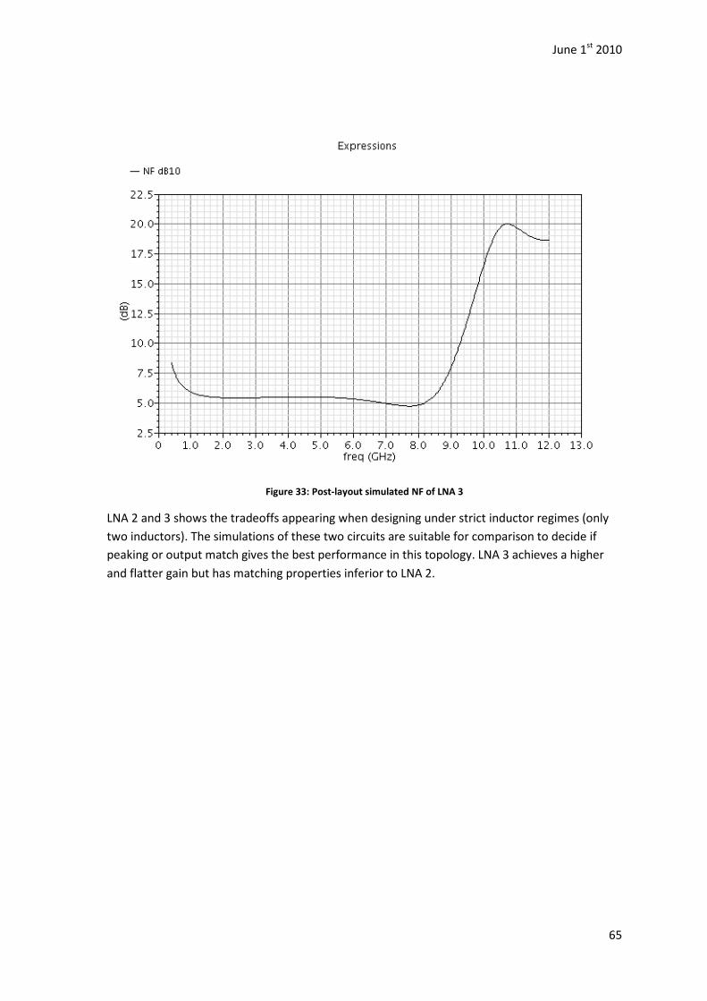
June 1st 2010
65
Figure 33: Post-layout simulated NF of LNA 3
LNA 2 and 3 shows the tradeoffs appearing when designing under strict inductor regimes (only
two inductors). The simulations of these two circuits are suitable for comparison to decide if
peaking or output match gives the best performance in this topology. LNA 3 achieves a higher
and flatter gain but has matching properties inferior to LNA 2.

CMOS Microwave LNA design
66
4.3.4 LNA architecture 4
The last architecture includes three gain stages and two inductors. LNA 4 uses a series input
matching, as LNA 1, a gain stage without peaking and a gain stage with splitting load peaking.
The architecture is shown in figure 34:
Figure 34: Schematic LNA 4
In this architecture the idea was to explore series input match and one peaking stage. The gain
stage in the middle was added to boost the gain without applying another inductor. This
increases the power consumption, but also increases the gain. The output match of this circuit
was based on tuning of the device sizes as in LNA 3. The input and output match is plotted in
figure 35:

June 1st 2010
67
Figure 35: Post-layout simulated S11 and S22 of LNA 4
The tweaking of this architecture gave improved output matching results in parts of the
bandwidth, compared to LNA 3. But still the output match is less than expected. The input match
is improved due to the series input approach used, and stays below -6 dB over the entire
bandwidth.
S21 and S12 are displayed in figure 36. The gain achieved is 12±2db from 0.3-8.6 GHz, which is
acceptable. Nevertheless, we would have expected higher gain from a three stage circuit
compared to the two stage circuits. The S12 is similar to the one achieved by LNA 1, and stays
below -40dB over the entire bandwidth.
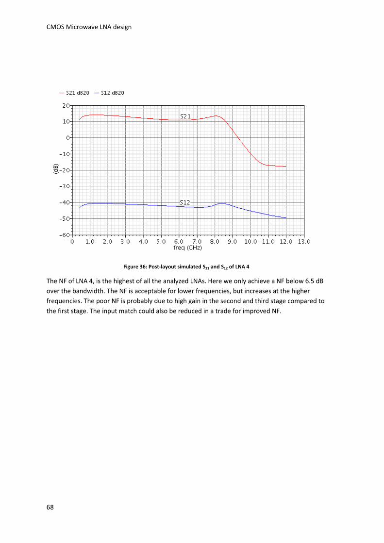
CMOS Microwave LNA design
68
Figure 36: Post-layout simulated S21 and S12 of LNA 4
The NF of LNA 4, is the highest of all the analyzed LNAs. Here we only achieve a NF below 6.5 dB
over the bandwidth. The NF is acceptable for lower frequencies, but increases at the higher
frequencies. The poor NF is probably due to high gain in the second and third stage compared to
the first stage. The input match could also be reduced in a trade for improved NF.
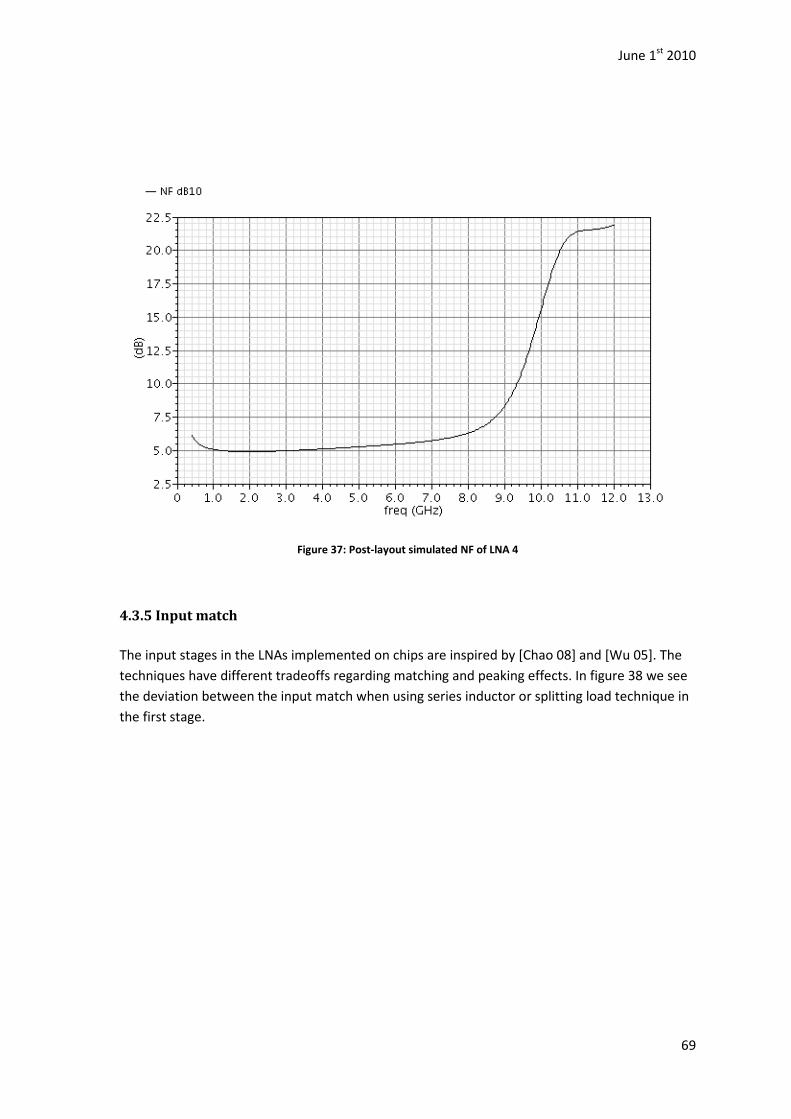
June 1st 2010
69
Figure 37: Post-layout simulated NF of LNA 4
4.3.5 Input match
The input stages in the LNAs implemented on chips are inspired by [Chao 08] and [Wu 05]. The
techniques have different tradeoffs regarding matching and peaking effects. In figure 38 we see
the deviation between the input match when using series inductor or splitting load technique in
the first stage.

CMOS Microwave LNA design
70
Figure 38: Post-layout simulated S11, series match versus splitting load technique
The splitting load has matching properties almost as a narrow band stage. The dip in the S11
response of the splitting load could be reduced in amplitude and widened in frequency by
decreasing the Q-factor of the input stage by connecting the inductor with a series resistor. This
was tried out late in the design phase but required a totally new tuning process and was
therefore dropped. The input matching with the series approach works quite well, with an
achieved input match of better than -6dB from 1-10.5 GHz and better than -8dB from 6 to 8.5
GHz. This is acceptable performance. The bonding wire is inductive and in series with the input,
and hopefully by making good bond wire models this could be integrated in the input match
with good results. The matching response of the splitting load seems to benefit from the idea of
designing custom inductors, i.e. low Q-factor for wider input match in addition to less area.
4.3.6 Output match
In the proposed topologies three different output matching techniques are implemented. These
are, tweaking of transistor and feedback resistor parameters, inductor in series with the NMOS
output and inductor in series with both output transistors. Simulations of these output matches,
S22, in post-layout are displayed in figure 39.

June 1st 2010
71
Figure 39: Post-layout simulated S22, no inductor versus inductor at NMOS and inductor in series
The output match without inductor has by far the poorest matching properties. This method of
matching showed promising results in schematic but, as shown earlier in this chapter, the output
was too capacitive in the extracted layout and the performance was degraded by 3-5 dB from 2
GHz and higher up in frequency. Based on the simulations and the layout tweaking process, it
seems like series inductor connection achieves the best output matching properties of the
inverter stages. The splitting approach proposed by [Chao 08] may contribute to a gain peak at
the highest frequencies, but this was not obvious from the explorations of these circuits.
4.3.7 Layout versus schematic
As mention above, post-layout simulations degraded performance significantly. This degradation
is due to parasitic components. Figure 40 shows the deviation in gain of LNA 1 from schematic to
layout.

CMOS Microwave LNA design
72
Figure 40: Simulated power gain, S21, of LNA 1 in schematic and post-layout
The gain is reduced with almost 8dB over the entire bandwidth, which is dramatic. The
bandwidth is reduced but not as much as the gain. The difference was almost of the same
magnitude when the process was switched from general purpose to low power, which was done
in the start of the design phase.
4.4 Simulated performance summary
A summary of layout performance of the architectures compared to measured performance of
other published works is displayed in table 6. In the gain column the ± sign displays the tolerance
of the gain in the bandwidth. The rest of the numbers are given as maximum gain and the
bandwidth between -3dB corner frequencies. The simulations have been carried out in a RF test
bench using input and output ports with characteristic impedance of 50 Ω. Corner simulations, in
the form of process and temperature variation simulation, have been performed in some of the
corners, but have not been a point of focus during the design.
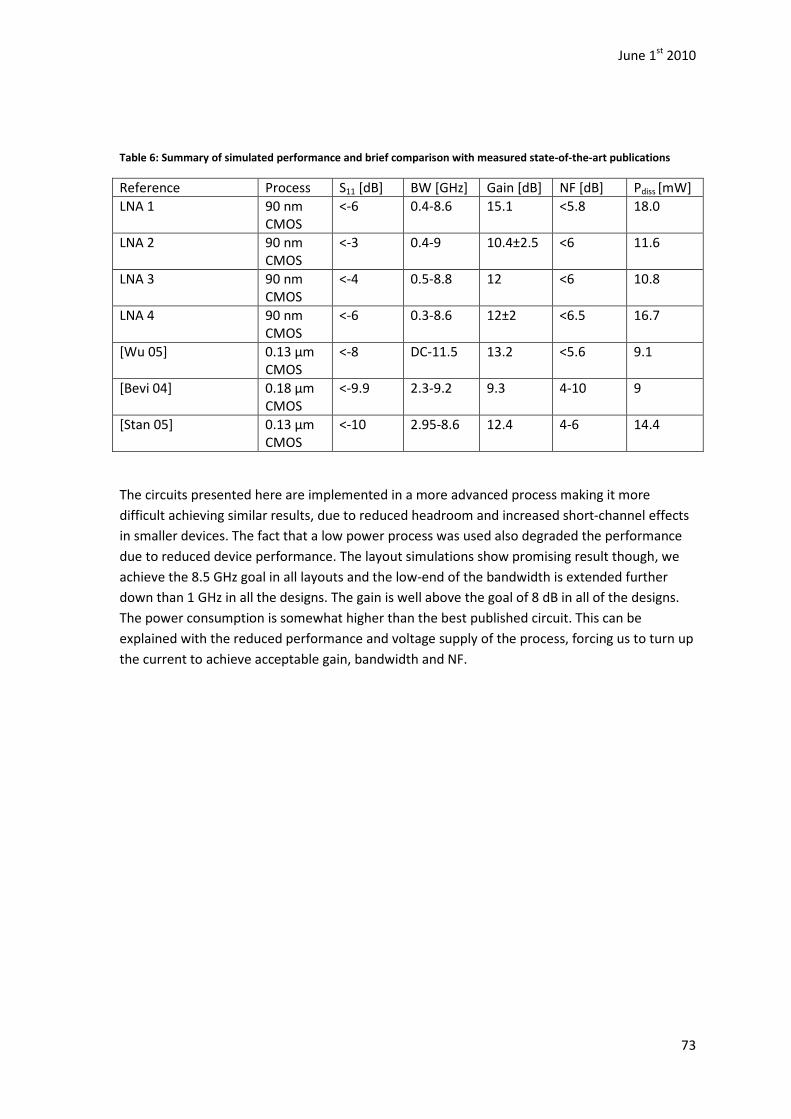
June 1st 2010
73
Table 6: Summary of simulated performance and brief comparison with measured state-of-the-art publications
Reference Process S11 [dB] BW [GHz] Gain [dB] NF [dB] Pdiss [mW]
LNA 1 90 nm
CMOS
<-6 0.4-8.6 15.1 <5.8 18.0
LNA 2 90 nm
CMOS
<-3 0.4-9 10.4±2.5 <6 11.6
LNA 3 90 nm
CMOS
<-4 0.5-8.8 12 <6 10.8
LNA 4 90 nm
CMOS
<-6 0.3-8.6 12±2 <6.5 16.7
[Wu 05] 0.13 µm
CMOS
<-8 DC-11.5 13.2 <5.6 9.1
[Bevi 04] 0.18 µm
CMOS
<-9.9 2.3-9.2 9.3 4-10 9
[Stan 05] 0.13 µm
CMOS
<-10 2.95-8.6 12.4 4-6 14.4
The circuits presented here are implemented in a more advanced process making it more
difficult achieving similar results, due to reduced headroom and increased short-channel effects
in smaller devices. The fact that a low power process was used also degraded the performance
due to reduced device performance. The layout simulations show promising result though, we
achieve the 8.5 GHz goal in all layouts and the low-end of the bandwidth is extended further
down than 1 GHz in all the designs. The gain is well above the goal of 8 dB in all of the designs.
The power consumption is somewhat higher than the best published circuit. This can be
explained with the reduced performance and voltage supply of the process, forcing us to turn up
the current to achieve acceptable gain, bandwidth and NF.
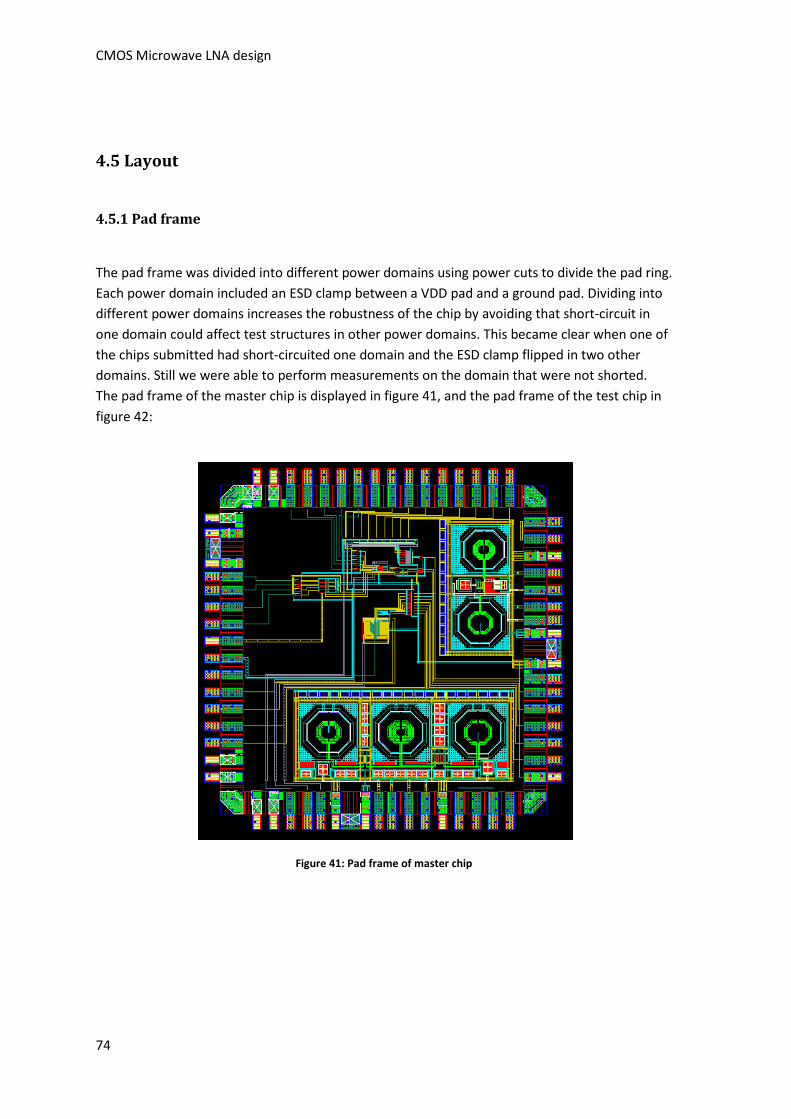
CMOS Microwave LNA design
74
4.5 Layout
4.5.1 Pad frame
The pad frame was divided into different power domains using power cuts to divide the pad ring.
Each power domain included an ESD clamp between a VDD pad and a ground pad. Dividing into
different power domains increases the robustness of the chip by avoiding that short-circuit in
one domain could affect test structures in other power domains. This became clear when one of
the chips submitted had short-circuited one domain and the ESD clamp flipped in two other
domains. Still we were able to perform measurements on the domain that were not shorted.
The pad frame of the master chip is displayed in figure 41, and the pad frame of the test chip in
figure 42:
Figure 41: Pad frame of master chip

June 1st 2010
75
Figure 42: Pad frame test chip
The pads used for input and output signals are analog pad. These should ideally be routed in a
higher metal layer than metal 2, but this was determined by the pads provided by the TSMC.
Higher metal layer (metal 7, 8 and 9), are thicker than the other metal layers, with the top metal
layer, layer 9, being the thickest. By routing in these layers we minimize the parasitic series
resistance introduced by the routing, and we minimize the capacitance to substrate since the
metal layers are further away from the substrate. This is illustrated with the basic formula for
capacitance:
= y>
Where A is the area of the wires or pad, d is the distance between the metal layer and substrate,
ε is the product of the dielectric constant of the material between the metal and substrate and
the electric constant (permittivity of free space ≈8.854*10-12 F/m). The pads are relatively large

CMOS Microwave LNA design
76
compared to routing on chip, making A large. Metal layer 9 will be further away from the
substrate, making d large and therefore reducing the capacitance to substrate (ground).
Each LNA were provided with two VDD pads to reduce the current density in the bonding wires,
improve the power distributing and reduce the inductance in series with the supply rail. Each
input and output of the LNAs has ground pads on both sides to reduce the amount of coupling
between the fragile input and output signal paths and other paths. By padding and bonding
ground on both sides there is minimal interference with the critical signal paths, and hopefully
this reduces distortion and can reduce the potential for oscillations as experienced in the front
end of [Hjort 06].
The input and outputs were routed to pads as close to the middle pads as possible. At the
middle pads the bonding wire to the pins shortest.
4.5.2 Layout strategies
We used some layout techniques to increase the robustness and the performance of the circuits.
The layout of LNA 1 is shown in figure 43, the rest of the layouts can be found in appendix A to C.
Figure 43: Layout of LNA 1
We made an effort in making the layouts symmetrical, this to minimize the difference between
the device environments and hopefully improve performance. Signal routing was done in wide
wires and Vertical Interconnect Access (VIA) connections were increased in size, all to minimize
the signal loss of the routing.
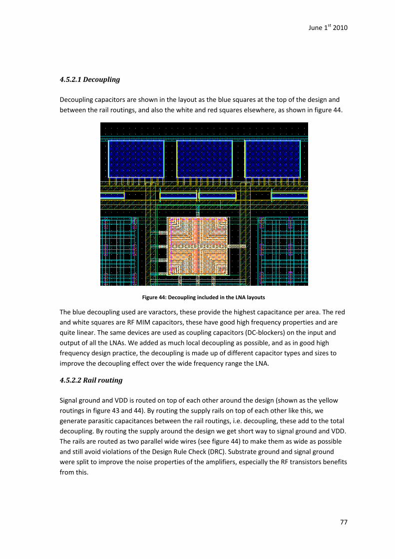
June 1st 2010
77
4.5.2.1 Decoupling
Decoupling capacitors are shown in the layout as the blue squares at the top of the design and
between the rail routings, and also the white and red squares elsewhere, as shown in figure 44.
Figure 44: Decoupling included in the LNA layouts
The blue decoupling used are varactors, these provide the highest capacitance per area. The red
and white squares are RF MIM capacitors, these have good high frequency properties and are
quite linear. The same devices are used as coupling capacitors (DC-blockers) on the input and
output of all the LNAs. We added as much local decoupling as possible, and as in good high
frequency design practice, the decoupling is made up of different capacitor types and sizes to
improve the decoupling effect over the wide frequency range the LNA.
4.5.2.2 Rail routing
Signal ground and VDD is routed on top of each other around the design (shown as the yellow
routings in figure 43 and 44). By routing the supply rails on top of each other like this, we
generate parasitic capacitances between the rail routings, i.e. decoupling, these add to the total
decoupling. By routing the supply around the design we get short way to signal ground and VDD.
The rails are routed as two parallel wide wires (see figure 44) to make them as wide as possible
and still avoid violations of the Design Rule Check (DRC). Substrate ground and signal ground
were split to improve the noise properties of the amplifiers, especially the RF transistors benefits
from this.

CMOS Microwave LNA design
78
4.5.2.3 The RF transistor
The RF transistors devices available in the component library are tighter specified than the
regular transistor devises, making them more ideal for high frequency designs. Deep n-well is
applied for isolating the substrate of the device from the global substrate. This results in less
substrate induced noise. A RF transistor is shown below:
Figure 45: Layout of RF NMOS provided by the design kit
RF transistors include double guard rings, which are necessary for NMOS deep n-well devices to
isolate the p-well (substrate) from the global substrate by completing the deep n-well. See cross-
section of deep n-well NMOS in figure 46.

June 1st 2010
79
Figure 46: Cross section deep n-well NMOS, from [Dahl 09]
The inner p-well of the RF NMOS transistor was connected to signal ground through a guard ring
while the n-well was connected to VDD through a guard ring. RF PMOS transistors also include
double guard rings, but then both are connected to VDD. When doing layout of the LNAs, yet
another ground guard ring was added outside RF transistors and connected to substrate ground,
improving the isolation even more, [Hast 01].
The Length of Oxide Definition (LOD) and Well edge Proximity Effect (WPE) are effects that have
become more and more significant in newer and more advanced processes. These effects are
explained in [Kana 07] and [Dren 07]. WPE is basically an effect that influences the threshold
voltages in MOS transistors. If we locate a PMOS to close the well boundary, the well will
become too shallow and increase the relative threshold voltage of the transistor. LOD effect is
an effect we found in finger transistors with shared drain or source terminals. The length from
the terminal to end of OD affects the parameters of the transistor. The LOD effect has opposite
effect on NMOS a PMOS, the PMOS becomes less conductive and the NMOS becomes more
conductive with increasing length to OD, for details see TSMC documentation of the process.
This effect is modulated in the layout extraction of the design kit, but not all schematic models
have modulated this effect. The RF transistor includes the LOD, STI and all other parasitic effects,
and behaves exactly the same in schematic as in layout. This alone is a reason good enough to
use the RF transistors, since the layout tweaking process most likely will be reduced because of
the improved correlation between layout simulations and schematic simulations.

CMOS Microwave LNA design
80
4.5.3.4 The on-chip inductors
The inductors include dummy area and a guard ring connected to substrate in the layout of the
device. Dummy areas have unconnected structures in all of the layers without active effect on
the circuit. These dummies are shown as the four groups of green squares around the inductor
in figure 47. Inside the octagonal surrounding of the inductor, there are not added additional
dummies and we can actually see the inductors on produced unpacked chips without using a
microscope.
Around the inductors a metal grid was routed for connecting the substrate to ground. See figure
47:
Figure 47: Inductor on chip with metal grid

June 1st 2010
81
These grids are shown as blue nets surrounding the inductor, and were added for improved
correlation between layout simulations and measurement. In the metal grids there were added
a large number of substrate connections (the small red rectangles in figure 47) making the
substrate potential as stable as possible around the inductors. The inductors are as mentioned in
earlier chapters, very large, this mainly because of the “safety zone” around the inductor and
the fact that the inductors are planar.
CMOS Microwave LNA design
82

5 Measurements
5.1 Chapter overview
This chapter will present the measurements of the LNA circuits, and the measurement setup
used.
5.2 Measurements
The measurements were carried out using custom made circuit boards
analyzer from Rohde&Schwarz. The circuits’ performan
due to limited time for measurements, problem analysis is at a minimum.
5.2.1 Printed circuit board design
We made two PCBs, one for LNA 1 and LNA 2 on the master chip, and another for LNA 3 and LNA
4 on the test chip. The two-layer PCBs were made in
The transmission lines on the PCBs were made as microstrip lines. A model of a microstrip line is
displayed in figure 48:
Figure
A is the microstrip which is milled in the top copper layer of the PCB. The wi
distance(C) from the ground plane (
impedance of the line. The substrate is a v
and the substrate chosen for this project was Rogers substrate. Rogers is an expensive substrate,
tightly specified for optimal performance at high frequencies.
3 Picture taken from: http://en.wikipedia.org/wiki/Microstrip
5.1 Chapter overview
This chapter will present the measurements of the LNA circuits, and the measurement setup
The measurements were carried out using custom made circuit boards, and a vector network
analyzer from Rohde&Schwarz. The circuits’ performances were not as good as expected
ue to limited time for measurements, problem analysis is at a minimum.
5.2.1 Printed circuit board design
We made two PCBs, one for LNA 1 and LNA 2 on the master chip, and another for LNA 3 and LNA
layer PCBs were made in-house using a milling machine.
The transmission lines on the PCBs were made as microstrip lines. A model of a microstrip line is
Figure 48: Cross-section of a PCB with microstrip line3
A is the microstrip which is milled in the top copper layer of the PCB. The width of this strip, the
distance(C) from the ground plane (D) and the dielectric constant of the substrate decides the
impedance of the line. The substrate is a very important factor in this sort of transmission lines,
and the substrate chosen for this project was Rogers substrate. Rogers is an expensive substrate,
tightly specified for optimal performance at high frequencies.
Picture taken from: http://en.wikipedia.org/wiki/Microstrip
June 1st 2010
83
This chapter will present the measurements of the LNA circuits, and the measurement setup
and a vector network
ces were not as good as expected, and
We made two PCBs, one for LNA 1 and LNA 2 on the master chip, and another for LNA 3 and LNA
house using a milling machine.
The transmission lines on the PCBs were made as microstrip lines. A model of a microstrip line is
dth of this strip, the
and the dielectric constant of the substrate decides the
ery important factor in this sort of transmission lines,
and the substrate chosen for this project was Rogers substrate. Rogers is an expensive substrate,

CMOS Microwave LNA design
84
The input and output of the LNAs were connected to microstrip lines designed with a
characteristic impedance of 50 Ω. The calculations of the width of these lines were done by the
design tool AppCAD from Agilent. The lines are 3.4 mm thick, which corresponds to the desired
impedance of 50 Ω with the Rogers PCB used. The PCB of the master chip was made as little and
simple as possible and is shown in the picture below:
Figure 49: PCB of master chip
The focus when designing the PCBs was to maintain an unbroken ground plane on one side,
avoid sharp angles in the input and output lines, and maintain a isolation distance of at least 2
mm for as long as possible (close to the pins this is impossible). Decoupling capacitors were
added to the supply rails, using standard high frequency design guidelines with four different
orders of magnitudes in device values. The decoupling was placed as close to the supply pin as
possible for minimizing the series resistance and inductance in wiring between the decoupling
and the supply pin. The different capacitor sizes provide different decoupling properties, in
respect to speed, charge and filtering, [Motc 93]. The supply lines and the input and output
patch are terminated with SMA (SubMiniature version A) connectors, a standard coaxial contact
with a characteristic impedance of 50 Ω.
The PCB of the test chip is displayed in figure 50, and was made mainly by a PhD student which
had test structures on the same chip.

June 1st 2010
85
Figure 50: PCB of test chip
The PCB of the test chip, have less decoupling and several voltage converters for supply. This
was implemented since future system chips will need to include microcontrollers operating at a
higher supply voltage than the chip, and thus requiring voltage converters for interfacing the
chip and share supply rails.
5.2.2 Measurements setup
The measurement setup is illustrated in figure 51. The measurements were carried out using a
vector network analyzer (ZVB 20) from Rhode & Schwarz. The vector network analyzer was
connected and controlled by a laptop through a LAN cable. The vector network analyzer
calculates the S-parameters automatically. This equipment is high sensitive and needs
calibration before performing measurements. To minimize the effect of the PCB, with was
significant, a PCB transmission line piece was made and included in the calibration.

CMOS Microwave LNA design
86
Figure 51: Measurement setup, inspirited by [Dahl 09]
The measurement lab is quite noisy. This noise was picked up by the transmission lines.
Therefore a simple Faraday cage was made and used during the measurement. This shielding
gave some attenuation of the high frequency noise.
The input power applied during the measurements was -10 dBm.
5.2.3 Measurement result
In the power domain of LNA 3, an ESD clamp was reversed connected, thus shorting the power
domain. This prevented measurement on LNA 3. The other LNA on the same chip, LNA 4, could
be measured.
The measurements performed and presented in the sections below, are somewhat
disappointing. All the LNAs seem to have stability problems in parts of the frequency sweep, and
the matching properties are degraded compared to simulations.
We are not able to measure the NF with the measurement equipment available, and therefore
are these measurement are left out.
5.2.3.1 LNA 1
LNA 1 was implemented on the master chip, using the master PCB shown in figure 49.
Measurement S11 and S22 matching performance of LNA 1 is plotted in figure 52.

June 1st 2010
87
Figure 52: Measured S11 and S22 of LNA 1
These results are somewhat surprising. The input match have a reflection above 0dB (total
reflection) from about 3.3 GHz to 5.6 GHz, and from 9.1 to 12 GHz. Total reflection in the input
match means, in theory, that no power reaches the input of the LNA. There is actually gain in the
reflection, meaning that the reflected voltage wave is larger than the incident voltage wave, i.e.
there is something resonating in the signal path. This affects the gain of the LNA at these
frequencies, as shown in figure 53.
The fast variation, almost noisy response, of the input- and output matches between 1.9 and 3
GHz, is harder to explain. This behavior also occurs in the input and output match of LNA 2, but
then at frequencies between 0.6 and 2.9 GHz, see figure 54. The bond wire test bench of the
master chip has the same response between 1 and 4 GHz, see figure 58. This effect does not
appear in the input and output match of LNA 4, see figure 56, or in the test benches
implemented on the test chip, figure 60. Since this response does not emerge in circuits
implemented on the test chip, it indicates that the master chip or the surroundings of the master
chip is the problem. The strange response appears on input, output, and test bench path. These
paths all have a transmission lines on the PCB of approximately the same length, and a bond
wire of nearly the same length. The transmission lines on the test chip PCB are of same
dimensions as on the master PCB, but the bond wire of the test chip, are shorter due to the
smaller package. The bond wires then stands as the most likely source of error in this case.
The measured gain, S21, and reverse gain, S12, is plotted in figure 53.

CMOS Microwave LNA design
88
Figure 53: Measured S21 and S12 of LNA1
We achieve a gain of 7.5-11.5 dB in the frequency range 0.3-3.6 GHz. The gain achieved here is
reduced compared to the simulation. But the result is tolerable and the gain reduction in this
frequency range, is almost within the limits we could expect when realizing the circuit in silicon.
The gain decreases after 3.6 GHz, most likely due to reduced matching quality, as mentioned
above. Two gain peaks occur at higher frequencies. Respectively a gain of 7- 12 dB between 5.4
and 5.7GHz, and a gain of 9-14 db between 7.4 and 7.9 GHz. These two peaks are probably
caused by the first two stages of the LNA 1, the first peak from the splitting-load stage and the
second peak from the input match stage. The input match of LNA 1 is improved in the frequency
range of the second peak. LNA 4, with the same input stage, also peaks at frequencies close to 8
GHz (10.6 dB at 8.2 GHz, see figure 56), however, without the improvement of the input match.
The series input stage is still likely the reason for these gain peaks in LNA 1 and LNA 4, since
there does not appear a peak, in this frequency range, in the response of LNA 2 (which applies
splitting-load input match).
The first peak in LNA 1 gain response (5.4-5.7GHz) occurs in a frequency range where the input
match is above zero in LNA 1, this substantiates the possibility of the peak being caused by
stored energy being released in the inductor of second gain stage at these frequencies. The peak
also appears in LNA 2 (6.5-9.5 dB, in the frequency range 5.6-6. 4 GHz), using stage identical
splitting-load stage, and therefore strengthen this theory.
Over 9 GHz is the input and output match of both circuits implemented on the master chip is
above 0 dB (figure 52 and 54), the same goes for the bond wire test bench of the same chip
(figure 58). This may indicate that the bond wires resonate at these frequencies.
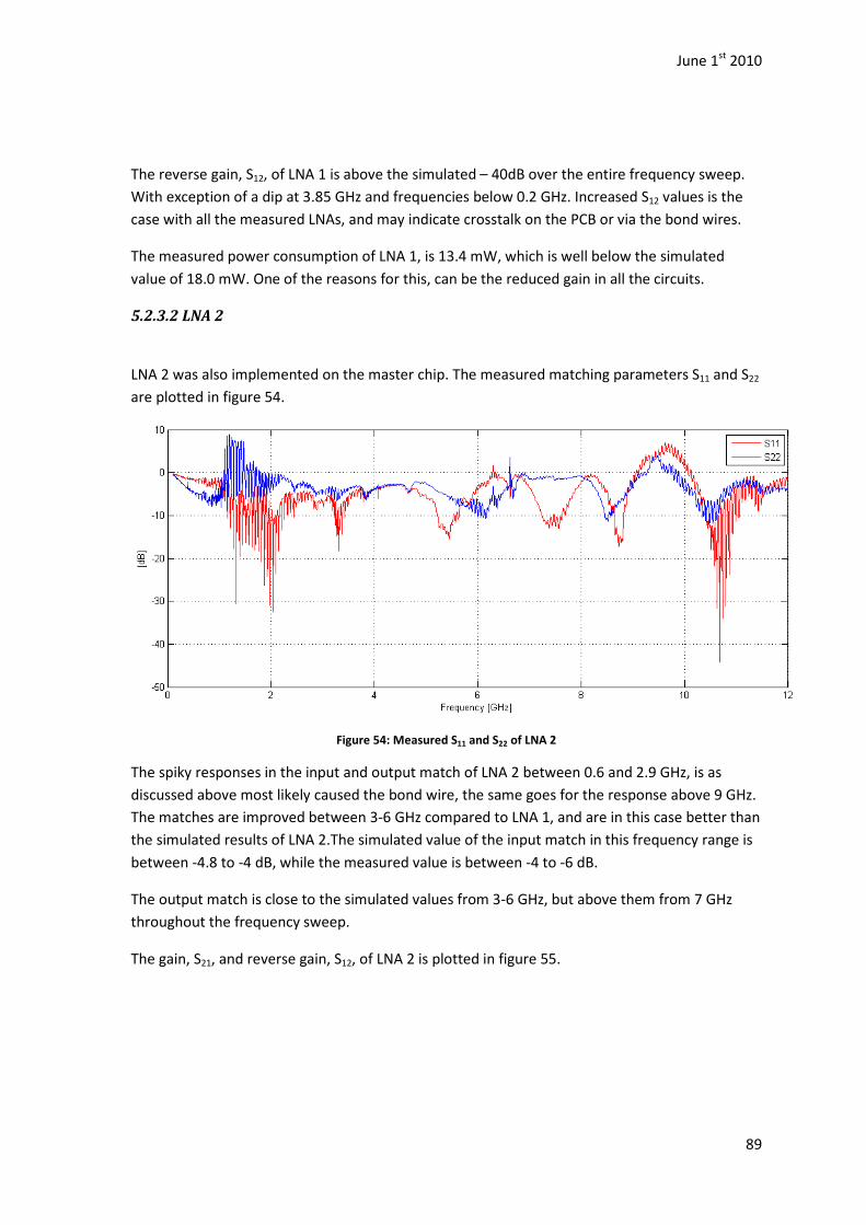
June 1st 2010
89
The reverse gain, S12, of LNA 1 is above the simulated – 40dB over the entire frequency sweep.
With exception of a dip at 3.85 GHz and frequencies below 0.2 GHz. Increased S12 values is the
case with all the measured LNAs, and may indicate crosstalk on the PCB or via the bond wires.
The measured power consumption of LNA 1, is 13.4 mW, which is well below the simulated
value of 18.0 mW. One of the reasons for this, can be the reduced gain in all the circuits.
5.2.3.2 LNA 2
LNA 2 was also implemented on the master chip. The measured matching parameters S11 and S22
are plotted in figure 54.
Figure 54: Measured S11 and S22 of LNA 2
The spiky responses in the input and output match of LNA 2 between 0.6 and 2.9 GHz, is as
discussed above most likely caused the bond wire, the same goes for the response above 9 GHz.
The matches are improved between 3-6 GHz compared to LNA 1, and are in this case better than
the simulated results of LNA 2.The simulated value of the input match in this frequency range is
between -4.8 to -4 dB, while the measured value is between -4 to -6 dB.
The output match is close to the simulated values from 3-6 GHz, but above them from 7 GHz
throughout the frequency sweep.
The gain, S21, and reverse gain, S12, of LNA 2 is plotted in figure 55.

CMOS Microwave LNA design
90
Figure 55: Measured S21 and S12 of LNA 2
The gain of LNA 2 is degraded compared to simulation, but there is achieved a gain of 7-10.4 dB
between 0.6- and 1.7 GHz. As mention under the section on LNA 1, there arises a gain peak of
6.5-9.5 dB in the frequency range 5.6-6. 4 GHz, probably caused by the splitting-load stage of
LNA 2. At the peaking LNA 2 actually delivers more gain than achieved in simulations. The peak
occurs at lower frequencies than in simulation, but this is not necessary an unreasonable change
from simulations when producing the circuit.
The measured power consumption in LNA 2 is 6.1 mW, which is well below the simulated value
of 11.6 mW. This power consumption is low compared to the published works presented in
chapter 4.
5.2.3.3 LNA 4
LNA 4 was implemented on the test chip, using a smaller package than the master chip. The PCB
used to conduct the measurements is shown in figure 50. A plot of the measured S11 and S22 , is
shown in figure 56.
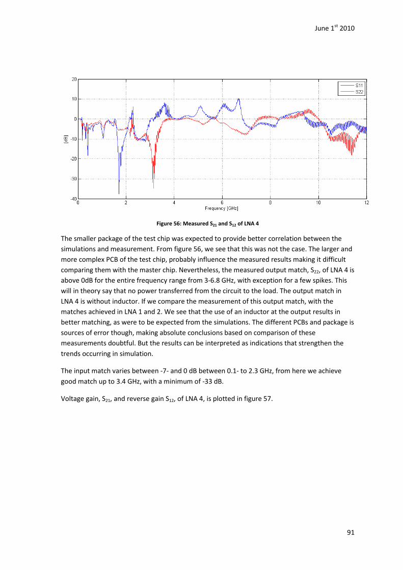
June 1st 2010
91
Figure 56: Measured S21 and S12 of LNA 4
The smaller package of the test chip was expected to provide better correlation between the
simulations and measurement. From figure 56, we see that this was not the case. The larger and
more complex PCB of the test chip, probably influence the measured results making it difficult
comparing them with the master chip. Nevertheless, the measured output match, S22, of LNA 4 is
above 0dB for the entire frequency range from 3-6.8 GHz, with exception for a few spikes. This
will in theory say that no power transferred from the circuit to the load. The output match in
LNA 4 is without inductor. If we compare the measurement of this output match, with the
matches achieved in LNA 1 and 2. We see that the use of an inductor at the output results in
better matching, as were to be expected from the simulations. The different PCBs and package is
sources of error though, making absolute conclusions based on comparison of these
measurements doubtful. But the results can be interpreted as indications that strengthen the
trends occurring in simulation.
The input match varies between -7- and 0 dB between 0.1- to 2.3 GHz, from here we achieve
good match up to 3.4 GHz, with a minimum of -33 dB.
Voltage gain, S21, and reverse gain S12, of LNA 4, is plotted in figure 57.
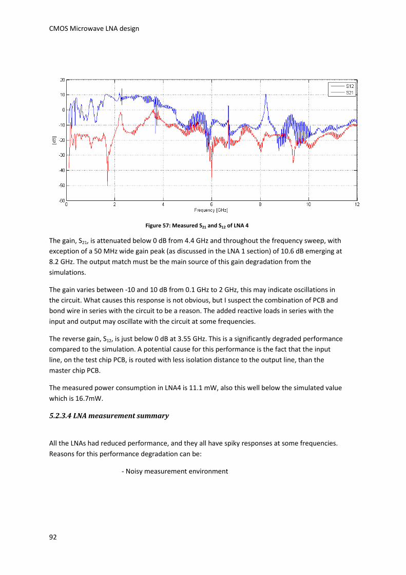
CMOS Microwave LNA design
92
Figure 57: Measured S21 and S12 of LNA 4
The gain, S21, is attenuated below 0 dB from 4.4 GHz and throughout the frequency sweep, with
exception of a 50 MHz wide gain peak (as discussed in the LNA 1 section) of 10.6 dB emerging at
8.2 GHz. The output match must be the main source of this gain degradation from the
simulations.
The gain varies between -10 and 10 dB from 0.1 GHz to 2 GHz, this may indicate oscillations in
the circuit. What causes this response is not obvious, but I suspect the combination of PCB and
bond wire in series with the circuit to be a reason. The added reactive loads in series with the
input and output may oscillate with the circuit at some frequencies.
The reverse gain, S12, is just below 0 dB at 3.55 GHz. This is a significantly degraded performance
compared to the simulation. A potential cause for this performance is the fact that the input
line, on the test chip PCB, is routed with less isolation distance to the output line, than the
master chip PCB.
The measured power consumption in LNA4 is 11.1 mW, also this well below the simulated value
which is 16.7mW.
5.2.3.4 LNA measurement summary
All the LNAs had reduced performance, and they all have spiky responses at some frequencies.
Reasons for this performance degradation can be:
- Noisy measurement environment

June 1st 2010
93
- Unfortunate PCB design with crosstalk and/or signal quality reduction
in the PCB lines
- The impact of bond wire, pad and transmission line on PCB
To improve the measurement results a different PCB transmission line technique could be
applied. Designing the PCB with shielding between the lines (making then planar waveguides),
could reduce crossover. On the test chip a more gradual cross-over from wide transmission line
to narrow path connecting the pin, could improve performance. This would reduce the
possibility of sudden impedance changes in the microstrip line causing them to act to some
degree like a microstrip component, [2Lee 04].
The measurement shows that the three LNAs we were able to measure on provide gain in parts
of the desired bandwidth, but unfortunately not for the entire bandwidth. The large impact of
the bond wire and PCB must take much of the blame for this degradation of the performance.
Much of the published architecture use measurement techniques probing directly on the wafer.
These techniques are widespread and I think that this is some of the reason for the little focus
on bond wire models in the published microwave amplifier literature. Despite the PCB design
probably being a large contributor to the performance degradation, I am surprised by the large
influence of the bond wire. To make a working prototype UWB LNA sample, improved PCB
design has to be applied and bond wire models have to be included in the design phase.
5.2.3.5 Bond wire and pad measurement
On the chips submitted two test benches for characterization of the bond wire were
implemented. These test benches consist of a bonded pad shorted to ground, and a non-
terminated (open) bonded pad. By measuring the S11 of these two test benches we are, in
theory, able to compute the impedance of the bond wire using the W.C Johnson [John 63]
procedure described in chapter 2.
The measured S11 result of the test bench implemented on the master chip is plotted in figure
58.

CMOS Microwave LNA design
94
Figure 58: Measured S11 of shorted and open bond wire test benches implemented on master chip
The large deviation in test bench S11 responses between the test chip and the master chip are
somewhat surprising. We would expect measurements of the test benches that correlated, this
is not the case for the entire frequency sweep and indicates that the PCBs influence the
measurements.
The rise above 0 dB above 9 GHz in the master chip responses indicates resonances or
calibration weaknesses in the calibration process of the measurement equipment. The
calculated absolute impedance value of the bond wire is plotted in figure 59.
Figure 59: Calculated absolute value of impedance in bond wire of master chip using W. C. Johnson Formula

June 1st 2010
95
Here two large impedance values occur, the largest at 5.3 GHz (over |1000 Ω|), and the second
largest at 9.5 GHz (|525Ω|). These two peaks are somewhat of a mystery, at least when no peak
close to this magnitude take place on the test chip. This must be taken as a sign of measurement
weakness or error. The PCB used for measurement on bond wire test benches on the test chip,
was custom made just for these measurements. I think this makes the test chip bond wire
measurement more reliable. To get reliable result from the test benches at the master chip, a
custom made PCB just for this should be made and the results verified on several chips.
The measurement performed on the test benches of the 48 pin is plotted in figure 60.
Figure 60: Measured S11 of shorted and open bond wire test benches implemented on test chip
These measurements are the least spiky of all measurement performed, and may be caused by
the more optimized PCB design. The calculated absolute impedance value of the bond wire and
pad, (based on the measurements in figure 60) is presented in figure 61.

CMOS Microwave LNA design
96
Figure 61: Calculated absolute value of impedance in bond wire of test chip using W. C. Johnson Formula
This calculated impedance has a response that looks capacitive at the start of the frequency
sweep. This is surprising since the bond wire is inductive. The pads are capacitive though, and
based on these measurements seems to be domination at frequencies below 1 GHz. The peaks
occurring around 5 and 9.5 GHz on master chip does not occur here. The lack of correlation
between the test benches on the two chips, makes it uncertain to compare the result and draw
conclusions on the basis of them.
The impedance responses of the bond wires vary with the package used, and both package
deviate from the expected response. I would have expected a response of these measurements
as a periodic pattern related to the response quarter wave microstrip stub lines [Ludw 09]. To
get more reliable results, custom made PCBs just for bond wire testing should be made, and
measurements should be carried out of several chips to validate the results.
On the bases of the measurements presented here, it is difficult to derive a reliable and simple
bond wire model. Complex models can be the case even with better measurement result, but a
possibility is to implement the response of the bond wires as a black box, and use it the design
kit when designing circuits.

June 1st 2010
97
6 Conclusion an proposal for future work
6.1 Conclusion
This thesis has presented four versions of a low-power UWB CMOS LNA, based on the topology
presented in [Chao 08]. The LNAs are design with as few inductors as possible for minimized size.
The proposed circuits show promising results in post-layout simulations, but the measurements
reveal that the circuits have problems maintaining the gain over the entire desired bandwidth.
There is achieved acceptable gain in parts of the frequency range, respectively 9.5±2 dB between
0.3-3.6 GHz, 9.5±2.5 dB between 5.4 and 5.7 GHz and 11.5±2.5 dB between 7.4 GHz and 7.9 GHz.
The LNAs should be fully functional for applications in these frequency ranges. Due to the limited
time available in this project, there have not been performed enough measurements to indentify
the sources for the degradation with absolute certainty. The analysis, simulations and
measurements presented in this thesis, should however provide a foundation for the
development of a working prototype, covering the entire frequency band, in the future.
6.2 Future work
To make a prototype circuit covering the entire UWB mask, the bond wire models have to be
characterized more systematically, and the results verified on several chips. A proper bond wire
model included in the design phase will probably dramatically improve the measured result of
the LNAs.
An improved PCB with shielding between signal paths should also be developed. The PCB seems
to be one of the main sources of error, and an improved design will increase the credibility of
the measurements, at least in the case of the bond wire characterization.
Since UWB LNAs are suitable for low Q inductors, custom made inductor models should be
explored. By reducing the area occupied by the inductors, we can increase the number of
inductors without increasing the size of the implemented circuit. With custom made inductor
models we can investigate other architectures, like the distributed amplifier and expand input
matching networks for improved match, solutions which were turned down in this project.

CMOS Microwave LNA design
98
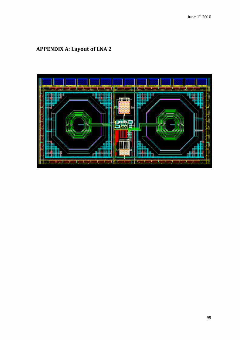
June 1st 2010
99
APPENDIX A: Layout of LNA 2

CMOS Microwave LNA design
100

June 1st 2010
101
APPENDIX B: Layout of LNA 3

CMOS Microwave LNA design
102

June 1st 2010
103
APPENDIX C: Layout of LNA 4
CMOS Microwave LNA design
104
June 1st 2010
105
References
[Bevi 04] A.Bevilacqua and A. M. Niknejad, “An
Ultrawideband CMOS Amplifier for 3.1-10.6-GHz
Wireless Receivers”, in IEEE Journal of Solid-State
Circuits, Vol 39, NO 12, December 2004
[Bluh 01] T. Bluhm, “S-parameters – Characteristics of Passive
Components”, BC components, 2001
[Cars 82] R.S. Carson, “High Frequency Amplifiers”, 2nd ed.,
Wiley, New York, 1982, p. 78.
[Chao 08] S-F. Chao, J-J Kuo, C-L. Lin, M-D- Tsai and H. Wang,
“A DC-11.5 GHz Low-Power, Wideband Amplifier
Using Splitting-Load Inductive Peaking Technique,”
in IEEE Microwave and Wireless Components
Letters, Vol 18, NO 7, July 2008
[Dahl 09] Ø. Dahl, High-precision beamforming with UWB impulse
radar, Master thesis, University of Oslo, Department of
Informatics, 2009
[Dren 07] P. G Drennan, M. L. Kniffin, D. R. Locasico
“Implications of Proximity Effects for Analog
Design”, Freescale Semiconductor, 2007
[Haji 03] A. Hajimiri, “Distributed Integrated Cricuits: Wideband
Communication For The 21st Century”, ENGenious, 2003
[Hast 01] A. Hastings, ”The Art of Analog Layout”, Person
Education, Inc., USA, 2001
[Heyd 07] P. Heydari, “Design and Analysis of a Performance-
Optimized CMOS UWB Distributed LNA,” in IEEE
Journal of Solid-State Circuits, Vol 42, No 9,
September 2007
[Hjort 06] H.A. Hjortland, UWB impulse radar in 90 nm CMOS,
Master thesis, University of Oslo, Department of
Informatics, 2006
CMOS Microwave LNA design
106
[John 63] W.C. Johnson, “Transmission Lines and Networks”,
McGraw-Hill, USA, 1963, p155
[Kana 07] T. Kanamoto, Y. Ogasahara, K. Natsume, K.
Yamaguchi, H. Amishiro, T. Watanabe and M.
Hashimoto, “Impact of Well Edge Proximity Effect
on Timing”, IEEE, 2007
[1Lee 04] T. Lee, “Planar Microwave Engineering: A Practical
guide to theory, measurement and circuits”,
Cambridge University Press, UK, 2004
[2Lee 04] T. Lee, “The Design of CMOS Radio-Frequency
Integrated Circuits”, 2nd ed., Cambridge University
Press, UK, 2004
[Ludw 09] R. Ludwig and G. Bogdanov, ”RF Circuit Theory and
Design”, 2nd ed., Person Education, Inc., USA, 2009
[Motc 93] C. D. Motchenbacher and J .A. Connelly, “Low Noise
Electronic System Design”, Wiley, Canada, 1993
[Sans 05] W. Sansen, “Low-power low-voltage design in
nanometer CMOS”, Talk at the University of Oslo,
August 2005
[Wang 05] S.B-T. Wang, Design of Ultra-Wideband RF Front-
End, Berkeley: PhD dissertation, University Of
California, Berkeley, 2005
[Wu 05] C-H. Wu, C-H. Lee, W-S. Chen and S-I. Liu, “CMOS
Wideband Amplifiers Using Multiple Inductive-
Series Peaking Technique”, in IEEE Journal of Solid-
State Circuits, Vol 40, No 2, February 2005