master thesis trygve k. halvorsen - universitetet i...
TRANSCRIPT

UNIVERSITY OF OSLODepartment ofInformatics
Power HarvestingMicroelectronics
Master thesis
Trygve K.Halvorsen
2nd May 2008


Abstract
Wireless communication is increasingly popular due to the human urgeto be independent and move around without being restricted by wires.With this trend come several challenges regarding both data transmissionand how to power the wireless tag. This thesis addresses some of thekey aspects of power harvesting, explores power harvesting capabilitiesin nanometer technology, but also consider different energy sources anddiscuss their adaptability to wireless identification tags. This thesis willalso present a novel charge pump, with improvements using the back-gateor well of MOS devices. The possibilities to improve efficiency, as well assensitivity, are discussed, and simulations, measurements and discussionof the results are provided at the end. The technology used is 90 nm CMOS.
iii

Abstract
iv

Preface
During the past five years I have attended the Master’s Degree Programin Microelectronics at Department of Informatics, Faculty of Mathematicaland Natural Sciences, University of Oslo. This thesis is submitted as a partof this program and concludes my work with the degree Master of Science.It was initiated in November 2006, and concluded in May 2008.
The work has been interesting and challenging in many ways, both dueto the approach to the subject and the subject itself. The main focus hasbeen the production of a chip in 90 nm CMOS technology and simulationsand measurements in this regard.
I would like to thank my supervisor Tor Sverre “Bassen” Lande for hisguidance and encouragement, driven by his passion for the subject and thegenuine interest in my work. I would also like to thank my co-supervisorHåkon A. Hjortland, which has been helpful and extremely valuable to mywork, and especially to the submissions of the scientific papers. And for agreat deal of help with PCB layout and measurements, my gratitude goesto Håvard K. Riis.
Next I would like to express my thanks to my closest classmates Sveinand Håvard. To Svein for his cooperation with the chip manufacturingprocess, and to Håvard for his expertice within the world of LATEX andlinux.
The great atmosphere among my fellow students at lab has been both aprofessional and social inspiration and has made the last two years cheerfuland productive.
And last, but not least, thanks to Sigrid for all the motivation.
Oslo, April 2008
Trygve K. Halvorsen
v

Preface
vi

Contents
Abstract iii
Preface v
Table of Contents vii
List of Figures xi
List of Tables xiii
1 Introduction 11.1 Motivation: The wireless world . . . . . . . . . . . . . . . . . 11.2 Previous work . . . . . . . . . . . . . . . . . . . . . . . . . . . 21.3 Thesis outline . . . . . . . . . . . . . . . . . . . . . . . . . . . 2
2 Background 52.1 History . . . . . . . . . . . . . . . . . . . . . . . . . . . . . . . 52.2 Systems and applications . . . . . . . . . . . . . . . . . . . . 10
2.2.1 Electronic Article Surveillance . . . . . . . . . . . . . 102.2.2 Electronic Product Code . . . . . . . . . . . . . . . . . 132.2.3 AutoPASS . . . . . . . . . . . . . . . . . . . . . . . . . 14
3 RFID and wireless power 173.1 Different RFID types . . . . . . . . . . . . . . . . . . . . . . . 17
3.1.1 Active tags . . . . . . . . . . . . . . . . . . . . . . . . . 173.1.2 Semi-active tags . . . . . . . . . . . . . . . . . . . . . . 173.1.3 Passive tags . . . . . . . . . . . . . . . . . . . . . . . . 18
3.2 Wireless power . . . . . . . . . . . . . . . . . . . . . . . . . . 193.2.1 Inductive link . . . . . . . . . . . . . . . . . . . . . . . 203.2.2 Microwave Power Transmissions . . . . . . . . . . . . 213.2.3 RF energy . . . . . . . . . . . . . . . . . . . . . . . . . 23
3.3 Frequency bands, calculations and measurements . . . . . . 253.3.1 900 MHz ISM band . . . . . . . . . . . . . . . . . . . . 253.3.2 2.4 GHz ISM band . . . . . . . . . . . . . . . . . . . . 25
vii

CONTENTS
3.3.3 Link Budget . . . . . . . . . . . . . . . . . . . . . . . . 273.3.4 Free space loss (FSL) and Friis’ formula . . . . . . . . 283.3.5 Calculation . . . . . . . . . . . . . . . . . . . . . . . . 29
4 Transmission of data 334.1 Analog modulation, AM and FM . . . . . . . . . . . . . . . . 334.2 Digital modulation, ASK and PSK . . . . . . . . . . . . . . . 344.3 UWB-IR . . . . . . . . . . . . . . . . . . . . . . . . . . . . . . 364.4 Surface Acoustic Wave filters (SAW filters) . . . . . . . . . . 38
5 Voltage boosting 415.1 Boost and Buck converters . . . . . . . . . . . . . . . . . . . . 415.2 Charge pumps . . . . . . . . . . . . . . . . . . . . . . . . . . . 44
5.2.1 The Dickson charge pump . . . . . . . . . . . . . . . . 445.2.2 The cascode charge pump . . . . . . . . . . . . . . . . 45
5.3 Adjusting threshold versus the leakage . . . . . . . . . . . . 475.4 Diode characteristics . . . . . . . . . . . . . . . . . . . . . . . 47
5.4.1 Adjusting the diodes . . . . . . . . . . . . . . . . . . . 495.5 Capacitors . . . . . . . . . . . . . . . . . . . . . . . . . . . . . 525.6 Dual charge pump . . . . . . . . . . . . . . . . . . . . . . . . 55
5.6.1 DC simulation . . . . . . . . . . . . . . . . . . . . . . . 555.6.2 AC simulation . . . . . . . . . . . . . . . . . . . . . . . 575.6.3 Process variations . . . . . . . . . . . . . . . . . . . . . 575.6.4 Layout of the charge pump . . . . . . . . . . . . . . . 60
5.7 Boostconverting of the charge pump output . . . . . . . . . . 61
6 PCB, chip and measurements 636.1 AC measurements . . . . . . . . . . . . . . . . . . . . . . . . . 646.2 DC measurements . . . . . . . . . . . . . . . . . . . . . . . . . 666.3 Power measurements . . . . . . . . . . . . . . . . . . . . . . . 686.4 Process variations . . . . . . . . . . . . . . . . . . . . . . . . . 686.5 Antenna measurements . . . . . . . . . . . . . . . . . . . . . 686.6 Reflection of the RF signals . . . . . . . . . . . . . . . . . . . 706.7 Discussion of the measurement results . . . . . . . . . . . . . 70
7 Alternative energy harvesting 737.1 Solar energy . . . . . . . . . . . . . . . . . . . . . . . . . . . . 73
7.1.1 p-n junctions, photovoltaic cells and photodiodes . . 737.1.2 PIN diodes . . . . . . . . . . . . . . . . . . . . . . . . . 767.1.3 Responsivity and quantum efficiency . . . . . . . . . 76
7.2 Kinetic energy . . . . . . . . . . . . . . . . . . . . . . . . . . . 777.2.1 MEMS-generators . . . . . . . . . . . . . . . . . . . . 77
7.3 Thermoelectric energy . . . . . . . . . . . . . . . . . . . . . . 787.3.1 Thermoelectrics - The Seebeck effect . . . . . . . . . . 79
viii

CONTENTS
7.4 Practical use of alternative energy sources . . . . . . . . . . . 82
8 Concluding remarks 858.1 Future work . . . . . . . . . . . . . . . . . . . . . . . . . . . . 86
9 Acronyms 89
A IC 93
B PCB 95
Bibliography 97
Paper 101
ix

CONTENTS
x

List of Figures
2.1 IFF . . . . . . . . . . . . . . . . . . . . . . . . . . . . . . . . . . 62.2 ISO members across the world . . . . . . . . . . . . . . . . . 82.3 Different types of Electronic Article Surveillance . . . . . . . 112.4 RFID supply chain . . . . . . . . . . . . . . . . . . . . . . . . 142.5 AutoPASS . . . . . . . . . . . . . . . . . . . . . . . . . . . . . 15
3.1 Auto-pass . . . . . . . . . . . . . . . . . . . . . . . . . . . . . 183.2 Skipass . . . . . . . . . . . . . . . . . . . . . . . . . . . . . . . 193.3 Inductive link . . . . . . . . . . . . . . . . . . . . . . . . . . . 213.4 Active Denial System . . . . . . . . . . . . . . . . . . . . . . . 223.5 Users of the 2.4 GHz ISM-band. . . . . . . . . . . . . . . . . . 273.6 Free space loss . . . . . . . . . . . . . . . . . . . . . . . . . . . 303.7 Antennas . . . . . . . . . . . . . . . . . . . . . . . . . . . . . . 31
4.1 AM and FM . . . . . . . . . . . . . . . . . . . . . . . . . . . . 344.2 ASK, PSK and FSK . . . . . . . . . . . . . . . . . . . . . . . . 354.3 UWB . . . . . . . . . . . . . . . . . . . . . . . . . . . . . . . . 374.4 SAW filter . . . . . . . . . . . . . . . . . . . . . . . . . . . . . 38
5.1 The input stage of a charge pump RFID-tag. . . . . . . . . . . 415.2 A conventional boost converter . . . . . . . . . . . . . . . . . 425.3 The states of a boost converter . . . . . . . . . . . . . . . . . . 435.4 Input and output of a boost converter . . . . . . . . . . . . . 435.5 The mother of all charge pumps: The Dickson . . . . . . . . 445.6 4-step cascode charge pump . . . . . . . . . . . . . . . . . . . 455.7 One step of the charge pump . . . . . . . . . . . . . . . . . . 465.8 Comparison of different MOS models . . . . . . . . . . . . . 485.9 The terminals of NMOS and PMOS transistors. . . . . . . . . 495.10 PMOS transistor with backgate connection . . . . . . . . . . 505.11 PMOS diode characteristics . . . . . . . . . . . . . . . . . . . 515.12 Diode characteristics with fixed amplitudes . . . . . . . . . . 535.13 CMOS capacitors . . . . . . . . . . . . . . . . . . . . . . . . . 545.14 Charge pump simulations . . . . . . . . . . . . . . . . . . . . 555.15 Dual charge pump . . . . . . . . . . . . . . . . . . . . . . . . 56
xi

LIST OF FIGURES
5.16 Testbench used to simulate the charge pump . . . . . . . . . 575.17 Time development of charge pump output . . . . . . . . . . 585.18 The AC component of the output voltage . . . . . . . . . . . 595.19 The changes in the circuit due to process variations. . . . . . 605.20 Boosting of the output with a pulse generator . . . . . . . . . 61
6.1 Test setup . . . . . . . . . . . . . . . . . . . . . . . . . . . . . . 636.2 Test setup used to measure the AC component of the outputs. 646.3 AC component. . . . . . . . . . . . . . . . . . . . . . . . . . . 656.4 AC component Test point. . . . . . . . . . . . . . . . . . . . . 656.5 Test setup used to measure the DC output voltage. . . . . . . 666.6 Output of the charge pump as a function of input amplitude. 676.7 Output of the charge pump as a function of input amplitude. 696.8 The reflection of the input terminal, S11, in terms of magnitude. 706.9 Two-port network . . . . . . . . . . . . . . . . . . . . . . . . . 72
7.1 p-n junction . . . . . . . . . . . . . . . . . . . . . . . . . . . . 747.2 Photovoltaic Cell . . . . . . . . . . . . . . . . . . . . . . . . . 757.3 Photodiode . . . . . . . . . . . . . . . . . . . . . . . . . . . . . 767.4 MEMS generator . . . . . . . . . . . . . . . . . . . . . . . . . 787.5 Seebeck effect . . . . . . . . . . . . . . . . . . . . . . . . . . . 807.6 Thermoelectric element . . . . . . . . . . . . . . . . . . . . . . 817.7 Thermopower of different materials . . . . . . . . . . . . . . 827.8 Commercial use of the technologies . . . . . . . . . . . . . . 83
A.1 Layout of the charge pump . . . . . . . . . . . . . . . . . . . 93A.2 Schematic of the charge pump . . . . . . . . . . . . . . . . . . 94
B.1 Layout of the PCB . . . . . . . . . . . . . . . . . . . . . . . . . 95B.2 Schematic of the PCB . . . . . . . . . . . . . . . . . . . . . . . 96
xii

List of Tables
2.1 RFID History . . . . . . . . . . . . . . . . . . . . . . . . . . . 10
3.1 Types of RFID-tags . . . . . . . . . . . . . . . . . . . . . . . . 183.2 Some of the ISM-bands within the EU . . . . . . . . . . . . . 233.3 Users of the 2.4 GHz ISM-band . . . . . . . . . . . . . . . . . 263.4 The best known classes of the IEEE 802.11 standard . . . . . 263.5 Maximum allowed transmit power in 2.4 GHz ISM-band . . 28
5.1 Capacitors in a STM 90nm CMOS process . . . . . . . . . . . 545.2 Monte Carlo simulation . . . . . . . . . . . . . . . . . . . . . 60
6.1 Specifications of Elprint PCB used. . . . . . . . . . . . . . . . 646.2 Measured output with 100mV input . . . . . . . . . . . . . . 66
7.1 Photodiode materials . . . . . . . . . . . . . . . . . . . . . . . 75
xiii

LIST OF TABLES
xiv

Chapter 1
Introduction
1.1 Motivation: The wireless world
In the 70’s, it was unimaginable for people to communicate with someoneor something, without being attached to the network physically. Now, 30years later, the term “wireless” has become a word everyone understandand can relate to, and even use to describe their own lifestyle. Picture,sound, video and other types of information are broadcasted, not just bybig companies, but also from household computer systems. This wirelessway of living raises countless possibilities, but also quite a few challenges.Security, adequate processing of personal data and ethical aspects are some,but the technology itself also has to meet the demands of an exacting trend.
Many of these technological challenges are power related. With theintroduction of identification tagging like Radio Frequency Identification(RFID) to the commercial market, the battery has lost its acceptance level.The consumers expect small devices, like road toll tags, to have unlimitedlifetime in some “magical” way. It is no longer considered outstanding,when devices are wireless and working.
As we can read in chapter 2.1, the history of the wireless identificationtechnology has moved fast forward and some very interesting aspectsare decreasing sizes, costs and increasing number of areas where thetechnology is used. To help this trend carry on, the power consummationand supply voltage will need to change dramatically. Supply voltages arepushed down to hundreds of millivolts, and the tags are becoming so smallthat embedded batteries not longer are a trivial part of the system. This,together with longer lifetime, means that power transmissions from thebase station or reader to the tag are becoming more and more important.Tags without batteries, called passive tags, are used commercially today,but with very limited use. This type of tags are restricted to very shortrange systems, and for ranges above 0.1 m tags with batteries, called activetags, are preferred.
1

Introduction
This work will investigate different power sources and design lowpower circuits for power supply purposes, with wireless identificationsystems in mind. RFID is today used to describe all wireless system thatidentify items in some way, and has become a quite vague term. Thisthesis is not exclusively concentrated around the RFID technology, butmore around the subject RFID as the term is used today, as a commondenominator for all systems using wireless tags.
1.2 Previous work
Since power harvesting is a huge subject there are many publications avail-able, and a selection of these articles and books are used as background ma-terial for this thesis. As a guide to general passive wireless communication,the work of Vipul Chawla [Chaw 07] and Dr. Jeremy Landt [Land 01] havebeen valuable sources. Another source of information that can be men-tioned is the seminar “RFID i næringslivet, status og trender”’ [RFID 07],which was a great inspiration for the background research on the commer-cial aspects of RFID. The circuit design purposed in chapter 5, which isthe main part of this work, is based on the discoveries of John F. Dickson[Dick 76], but the modification to a cascode charge pump is inspired byKarthaus and Fisher’s [Kart 03] article from 2003.
1.3 Thesis outline
This thesis starts with presentation of the history and basics of wirelessidentification technology, frequency calculations and transmission meth-ods. Further, the main part of the thesis is the design of a novel Radio Fre-quency (RF) charge pump, followed by the data from the measurements. Areview of three different alternative energy sources composes the last chap-ter. The paper written about the charge pump is enclosed in the back of thethesis, and describes the charge pump in detail.
• Chapter 1 gives a short introduction to the subject, previous work,why this subject is chosen and this outline of the thesis.
• Chapter 2 presents the history of wireless identification and RFID andsome examples of specific systems using this technology.
• Chapter 3 describes the basics behind the technology, a overview ofcertain frequency bands and a link budget.
• Chapter 4 presents various transmission methods used by wirelesstags and communication systems.
2

Introduction
• Chapter 5 is the part of the thesis where a circuit is designed andfabricated.
• Chapter 6 presents the measurement data extracted from the chipdesigned in chapter 5, and discusses the collected data.
• Chapter 7 reviews different alternative energy sources, both conven-tional and more experimental. A comparison of these follows at theend of the chapter.
• Chapter 8 summarizes the work, and give some suggestions to futurework.
• The appendixes, A and B, contains figures of the charge pump andPrinted Circuit Board (PCB).
• The paper written about the charge pump is enclosed in the back.
3

Introduction
4

Chapter 2
Background
To get an understanding of the subject we first have to take a look at thehistory of wireless identification.
2.1 History
When looking back on the history of communication using reflected energy,the subject is quite big. It spans from passive filter tags to radar technology,and is applicable on several different areas. The idea of using radiobackscattering to identify objects was used as early as pre-World War II,and the technologies behind were described even earlier.
We can say that RFID and wireless identification was born duringthe World War II. The Germans discovered that the reflected radio signalwould change if pilots rolled their planes returning to the their homebase. This simple method, at least technological simple, gave the base theopportunity to tell that these planes were German and not allied aircraft.Further, the Royal Airforce (RAF) also had a way to identify friendly planescalled Identification Friend or Foe (IFF), invented in 1939. The IFF systemsused coded radar signals called Cross-Band Interrogation (CBI) to triggerthe friendly aircraft’s transponder automatically when entering the radarzone. When the friendly aircraft "answered" at a certain frequency, theplanes appeared brighter on the radar screen that other aircrafts.
At the end of this war, in 1946, Léon Theremin invented an espionagetool for the Soviet Union. This device retransmitted incident radio waveswith audio information and the vibrations of the sound waves made adiaphragm move. This slightly altered the shape of the resonator, whichmodulated the reflected radio frequency. The listening device of Theremincan hardly be classified as a RFID tag, but still is considered as the firstknown RFID device, or at least the predecessor to the modern RFID tag.
In 1948 Harry Stockman published his paper "Communication byMeans of Reflected Power" [Stoc 48] which turned out to be an important
5

Background
Figure 2.1: The basics of “Identification Friend or Foe”
article in the development of RFID. Amongst other things, Stockman pre-dicted that "Considerable research and development work has to be donebefore the remaining basic problems in reflected-power communication aresolved, and before the field of useful applications is explored." With thiswords, the foreseeing Stockman stated an allegation that is just as relevanttoday. Problems regarding reflected power are still researched, and withthe progress of this research, the field of useful applications is expanding.
In the 1950s and 1960s the advances in radar and RF technologycontinued, and several papers on how to use RF energy to identify remoteobjects were written. A commercial breakthrough was the introductionof anti-theft tags in retail stores, which was the start of what is nowknown as Electronic Article Surveillance (EAS). EAS has been, and stillis, a major part of the RFID technology and will be further explained inchapter 2.2.1 on page 10.
In the 1960s inventors also started to see the possibilities the technologyoffered, and several more or less usable inventions was born. RobertRichardson’s article about “Remotely activated radio frequency powereddevices” from 1963 and Otto Rittenback’s “Communication by radarbeams” in 1969 are two important works from this period. Richardson’sarticle describes a device that can rectify a coupled energy from aninterrogator’s EM field, and transmit signals at a harmonic frequency ofthe received signal. These early RFID systems mainly used well knowntransmission methods, like radar technology, altdough in another scale.Still the inventions were very innovative, and during this period this trendalso helped other branches of the telecommunication industry to evolve.
6

Background
Near field devices were also popular in this period, and the inductive linkgot reborn, this time in the commercial arena.
The 1970s showed the world RFID research laboratories and a great dealof developmental work. Developers, inventors, companies, governmentsand especially academic institutions were actively working with RFID tech-nology, and several research laboratories were founded. Amongst the insti-tutions researching RFID in the 70s were the Los Alamos Scientific Labora-tory, Northwestern University and the Microwave Institute Foundation inSweden some of the most influential. Large companies like Fairchild andRadio Corporation of America (RCA) (now Thomson SA) started to de-velop RFID technology and in 1973 Raytheon launched the “Raytag”. TheRaytag was the first device used for animal tagging to track migration pat-tern, and was soon to be followed up by Richard Klensch of RCA and his“Electronic identification system” in 1975. In 1977 the “Electronic licenseplate for motor vehicles” was developed by Fred Sterzer (RCA). Vehiclescanning systems in big scale were tested in the 70s, and one example ofthis was when the Port Authority of New York and New Jersey tested var-ious systems from General Electric, Westinghouse, Philips and Glenayre.These systems were promising, but not yet adequate. During a conferenceheld by the International Bridge Turnpike and Tunnel Association (IBTTA)and the United States Federal Highway Administration in 1973, the con-ference concluded that there was no national interest in developing a newstandard for electronic vehicle identification. Once again, the technologywas not ready to hit the market.
In the 1980s the same trend continued, with further commercializationand new patents rolled out of the research facilities. While the scientists inthe United States aimed towards transportation and personnel access, theresearch in Europe focused on short-range tracking of animals, industrialtracking, factory automation and electronic toll collection.
In 1987, 14 years after the US rejected the technology, the electronictoll collection was launched. By the end of October 1987 the first RFID-based toll collection system was up and running in Ålesund, Norway. Thiswas a big breakthrough for RFID, since this system showed good quality,even in commercial use. This system was implemented by the Swedishcompany Combitech AB, which later was bought by Austrian Kapsch. Notlong after this breakthough RFID based toll stations were to be seen intoll roads in Italy, France, Spain and Portugal too. This trend was soonto be adopted across the world and “across the pond” the Associationof American Railroads and the Container Handling Cooperative Programwere active with RFID initiatives. The Port Authority of New York andNew Jersey picked up were they had left in the 70s, and began commercialoperation with RFID. This process started with tagging of buses goingthrough the Lincoln Tunnel, but expanded quickly to other areas.
RFID was now used in several arenas and this use prompted a need
7

Background
for standards. During the 1990s the standardization was mainly controlledby the International Standards Organization (ISO) and International Elec-trotechnical Commission (IEC). ISO is an international standard-setting or-ganization with representatives from nearly all national standards orga-nizations in the world. The organization with headquarters in Geneva,Switzerland, was founded in 1947 and declares world-wide industrial andcommercial standards. ISO is a non-governmental organization, but stillthe decisions made by this organization often become law across the world.
Figure 2.2: ISO members are marked by a green color, correspondent mem-bers by yellow, subscriber members in red and non-members are shown inblack. (Courtesy of the International Organization for Standardization)
IEC is a similar non-profit, non-governmental global organization, andworks with standards for electrical, electronics, and related technologies.More specific, the IEC covers a wide range of technologies such as batter-ies, power generation, transmission and distribution, home appliances andoffice equipment, fiber optics, semiconductors, solar energy, micro- andnanotechnology and marine energy. Some of the “famous” standardiza-tions are color marking of resistors, capacitors and inductors, known as theelectronic color code (IEC 60062), the standardization of the RJ45 connector(IEC 60603-7), the VHS video tape cassette system (IEC 60774) and semi-conductor devices (IEC 60747). The IEC collaborates with the Institute ofElectrical and Electronics Engineers (IEEE), the ISO and the InternationalTelecommunication Union (ITU). IEC, founded in 1906, counts more than130 countries and 69 of these are active members.
The standardization of animal tracking devices (ISO-11784 and ISO-11785) and contactless proximity cards (ISO-14443), were the first standard-izations that regarded RFID. With standardization came the possibilities tocooperate across systems, and the first cooperative RFID system was a sys-tem based on the Title 21 standard installed on the Kansas turnpike. This
8

Background
system had readers that could also operate with tags from the Oklahomatoll systems. This made it much easier for the consumers, since only one tagwas needed when travelling between the states. Georgia soon followed upwith readers that could communicate with the new Title 21 tags as well asthe existing tags, and the standardization proved to be a success. This wastaken futher by the 12-county Dallas-Fort Worth-Arlington metropolitanarea. They used a single tag, titled TollTag, to pay tolls on the North DallasTollway, parking payment at the Dallas International Airport, Dallas LoveField airport, downtown parking garages and to access gated communitiesand business facilities.
The interest both in Europe and the US was now turned once againtowards access and control systems, and both microwave and inductivetechnologies were used in this purpose. Texas Instruments developed theirTIRIS system with success and the TIRIS was used in cars and trucks tocontrol starting of the engine. This system, together with other similarsystems, developed new applications. Fuel dispensing, ski passes, andvehicle access were some of them.
A milestone in the history of RFID came in 1996, when RFID becamestandardized as a data carrier by the Article Number Association (ANA)and European Article Numbering (EAN) groups. The EAN Internationaland the Uniform Code Council (UCC) (Now both known as GS1 togetherwith the Electronic Commerce Council of Canada (ECCC)), adopted in1999 a UHF frequency band for RFID and later founded the Auto-IDCenter at the Massachusetts Institute of Technology (MIT). The Auto-IDCenter was the predecessor to Auto-ID Labs and EPCglobal, and laterdeveloped the Electronic Product Coding (EPC), which is a standard forelectronically labeling products with RFID. EPC will be further discussedin chapter 2.2.2 on page 13.
Another breakthough in this decade was the advances in silicontechnology, which made silicon based RFID tags cheap and reliable. Usefulmicrowave Schottky diodes were now possible to fabricate with regularCMOS integrated circuits, and this led way for construction of microwaveRFID tags on a single integrated circuit. Lower costs and risks regardinghardware failure made it possible to run large-scale projects. Tags becamecheaper and smaller, and could be used to tag smaller and cheaper items,like the products sold at Wal-Mart. Wal-Mart Inc., an American chain oflarge, discount department stores, launched in the early 2000s one of thelargest and best known RFID projects until now. Tagging that many itemsis a demanding job. To make this project doable, they also demanded theirsuppliers to implement this system, and at the Retail Systems Conferencein June 2003 in Chicago, they presented the system. The release of the firstEPCglobal standard followed in January 2005. Wal-Mart, which was thelargest public corporation in the world by revenue in 2007, now have morethan 1000 stores with EPC RFID standard implemented.
9

Background
Table 2.1: The RFID History summarizedDecade Event
1940 - 1950Radar refined and used, major WWII development effort.
RFID invented in 1948.
1950 - 1960Early explorations of RFID technology.
Laboratory experiments.
1960 - 1970Development of the theory of RFID.
Start of applications field trials.
1970 - 1980Explosion of RFID development.
Tests of RFID accelerate.Very early adopter implementations of RFID.
1980 - 1990Commercial applications of RFID enter mainstream.
First electronic road toll collection.
1990 - 2000Emergence of standards.RFID widely deployed.
RFID becomes a part of everyday life.
2.2 Systems and applications
The possibilities with wireless technologies are many, and as we have seenduring the past 50 years, the number of areas where RFID and similarsystems are used, expands rapidly. Not only systems developed for a singlepurpose, but also standards. In this chapter a few specific systems fromthe most common areas will be described to give an understanding of theway large RFID systems and standards works. EAS uses different typescommunication methods and is a good place to start when entering theworld of energy harvesting and wireless tags.
2.2.1 Electronic Article Surveillance
EAS was one of the first commercially used systems that identified objectsusing RF or inductive link, and is an important part of the security systemof a retail store. The technology is used to identify items or merchandisewhen they pass through the exit or a gated area, and is implementedto prevent unauthorized removal of items from a store, library or otherplaces where shoplifting occurs. The systems consists of three components;tags or labels (sensors) that are attached to merchandise, deactivatorsor detachers to use by the clerks, and finally detectors that create asurveillance zone at the exits. There are several different EAS systemsavailable on the marked, but common for them all is that an EAS tag orlabel is attached to the item. When the item is purchased or borrowed, thetag is detached or deactivated and the item can be carried out of the storewithout setting off the alarm. By using an EAS system, it is not necessary
10

Background
to lock the product away, which makes it easier for the consumer to reviewthe product. The cost of tagging all the products is also decreasing, as manysuppliers now build the tag into the product at the point of manufacture orpackaging. This saves both money and time in the stores and makes itharder for shoplifters to remove the tags.
The choice of which communication method to use depends on manyfactors. The technology affects the ease of shielding, the visibility and sizeof the tag, the rate of false alarms, detection rate and cost. Even if thedifferent methods seem equal to the untrained eye, todays EAS systemscan be divided into four different categories:
• Electromagnetic
• Acoustomagnetic, also known as magnetostrictive
• Radio frequency
• Microwave
Figure 2.3: Different types of Electronic Article Surveillance. (Courtesy ofAssociation for Automatic Identification and Mobility)
11

Background
Electromagnetic
The electromagnetic EAS system uses the detectors to generate a lowfrequency electromagnetic field, in the frequency range of 70 Hz to 1 kHz.This field will change strength and polarity when repeating the cycle frompositive to negative and back. And with each half cycle, the polarity ofthe magnetic field changes. This alternating magnetic field created by thetransmitter will affect the tag, and this sudden change in the magnetic statewill generate a signal from the tag. This signal will have lots of multiples ofthe fundamental frequency, also called harmonics of the original frequency.The reader will then detect these harmonics by frequency, strength andtime in relation to the transmitter.
Acoustomagnetic
Acoustomagnitic EAS is quite similar to the electromagnetic, but operatesat a higher frequency. The transmitter sends a signal at 58 kHz in pulses,and power the tags in the surveillance area. The tag works like a tuningfork, and replies to the reader with a frequency close to the transmittersignal. In order to detect the tag that replies at the same frequency as thetransmitter is using, the reader have to listen for tags between the pulses ofthe transmitter when the transmitter is off. If a signal with this frequencyis detected when the transmitter is quiet, the alarm is activated.
Swept radio frequency
This method differs from the magnetic methods because the frequency isnot fixed, but the RF - EAS sweeps the frequency between 7.4 MHz and8.8 MHz. This signal energizes the tag, which in this case is often more likea sticker with copper wires called a label. This label contains a capacitorand an inductor, and the components are able to resonate when connectedtogether in a loop. The frequency which the transmitter operates at, hasto be matched with the component values in the label. The emitted signalfrom the label can be distinguished by the reader in order to detect thelabel.
Microwave
As figure 2.3 on the preceding page shows, this type of EAS look quitedifferent than the other three. The system is composed of a transmitter, asynchronous receiver, a microprocessor-controlled detector and an alarm.The transmitter generates two different signals in the surveillance area,one high frequency carrier signal and one low frequency signal. Thehigh frequency signal is in Europe between 2402 MHz and 2486 MHz,and in North America between 902 MHz and 906 MHz. This is to
12

Background
avoid interference with other systems, since the frequency regulations aresomewhat different in different parts of the world. The low frequencysignal is a modulation signal and operates at 111.5 kHz. This signal is anon-propagating, electrostatic signal to limit the RF field to the surveillancezone. The tag in this system consists of a microwave diode and an antenna.This antenna is tuned to receive the signals from the transmitter and whenthe tag is in the surveillance zone, the tag combines the two signals andreflect the combined signal to the receiver. The modulation of the highfrequency signal with the low frequency signal is amplified by the receiverand compared to a reference signal to make sure when to activate the alarmor not.
2.2.2 Electronic Product Code
The barcode has been a key part of product labelling since JosephWoodland and Bernard Silver patented the first bar code system on October7, 1952 [Shep 04]. Almost every product in the world is identified with abarcode, even if it is a carton of milk at the grocery store or spare partsat a warehouse. The main drawback with barcodes is that they have tobe visible to be read. Dirt, rifts, interference with other objects or wrongalignment can cause reading problems. With the introduction of RFIDto the commercial market, the barcode got competition. The advantageswith RFID over barcodes are many, but both cost, security and complexityissues have held RFID back. Now that the prices have decreased and RFIDhas become more mainstream, it has replaced barcodes in several arenas.And as described in chapter 2.1 on page 5, Wal-Mart’s implementation ofRFID it probably the most famous example. With widespread use of RFIDsolutions to identify items, standards were needed.
EPC is a group of coding schemes created to replace the bar code withtime, which was created by MIT at the Auto-ID Labs as a low-cost methodof tracking goods using RFID. It is designed to work like the barcode,guaranteeing uniqueness and to fit various industries and products. Incomparison to the barcode, the EPC tags are designed to identify each itemmanufactured, whilst the barcode only identify the manufacturer and classof products. The EPC standard, which today is managed by the EPCglobal,will probably become the global standard for RFID, and a core element ofthe proposed EPCglobal Network. The reason why some many store chainsand industries are planning to, or already are using EPC, is that RFID alsocan be used as a tracking device all along the supply chain. The currentEPC version is 96-bit and contains information about the manufacturer,the product class and a specific serial number that identifies that specificobject. This gives the buyer the opportunity to follow the product allthe way back to the factory and even implement extra functionality liketemperature-sensors on frozen products. All this can be logged, the supply
13

Background
Figure 2.4: RFID used to track and identify items in every step of the logisticprocess. (Courtesy of DC Logistics)
chain can be made more effective and the facts regarding products that are"dead on arrival" are easier revealed. This can be done across borders andcompanies, if your partners also use EPC.
The future challenges for EPC based RFID are the technology. Tagshave to be cheaper, the reading distance longer, and the ability to readseveral tags at once will have to improve. The promising EPC standardis already existing worldwide, but as we have seen throughout the history,the technology will have to mature before the standards and ideas can workcommercially.
2.2.3 AutoPASS
There are many different electronic road toll collection systems in usearound the world, but we will now take a closer look at the one used inOslo, Norway. The development work of the Autopass system startedin 1998, as the successor to the Surface Acoustic Wave (SAW) tags whichis described in chapter 4.4 on page 38. Some of the motivation for anew system was that the frequency previously used, 856 MHz, was underconcession by the Norwegian Post and Telecommunications Authority(NPT) for digital TV. The new system, AutoPASS, was launched late 1999and operates at 5.8 GHz with semi-active tags (See chapter 3.1). Since thestart in 1999, the 3. generation toll system is implemented at almost 30
14

Background
other toll roads, making the system one of the most modern and populartoll systems in Europe.
Figure 2.5: With AutoPASS you can pass the toll collection even at highspeeds.
The tags used in the AutoPASS system are using Amplitude ShiftKeying (ASK) and Phase Shift Keying (PSK) (see chapter 4.2 on page 34)for receiving and transmitting respectively, has a max reading distance of10 meters and an expected battery lifetime of about 5 years. The EuropeanCommittee for Standardization/Comité Européen de Normalisation (CEN)is currently working on a European standard for electronic road tollcollection and AutoPass will be a part of this standard. The idea is to makeit able for all Europeans to use the same tag in every toll road across Europe.For AutoPASS, this partnership is today limited to the Nordic countries,and the AutoPASS tag can be used at several large toll roads and bridges inSweden and Denmark in addition to most Norwegian toll roads.
15

Background
16

Chapter 3
RFID and wireless power
In order to design a working RFID tag, the way of powering the tag is animportant issue. The choice of energy source and transmission method iscrucial and strongly depends on the use and environment of the tag. Manydifferent solutions have to be considered, and operating radius, fabricationcosts and size are usually the factors that will point out which type of tagto use. RFID tags can be classified into three main categories; active, semi-active or passive.
3.1 Different RFID types
3.1.1 Active tags
Active RFID-tags completely rely on a battery to operate, and therefore cantransmitt data in the absence of an RFID reader or an external energy source[Shep 04]. This type of tags are widely used in various applications, but arethe most expensive type of tag because of the battery, and also becauseactive tags are often more complex in design. There are many fields ofusage where an active tags can be used, but the use is limited as the batterywill need replacement. If the battery lifetime is a problem, i.e. in medicalimplants, a semi-active or passive tag can be used.
3.1.2 Semi-active tags
Semi-passive tags also have an embedded battery to power the tag, butoperate somewhat differently. Normally, this battery is only activatedwhen the tag is in the range of a reader. This will result in longer batterylifetime since the tag is not constantly transmitting data. Still, semi-activetags operate at long ranges, but the size of the tag is often conciderablelarger than passive tags. A well known example of semi-active tagsused commercially is the AutoPASS system, which is used as a payment
17

RFID and wireless power
Table 3.1: Compression of the different types of RFID-tags.Battery Range Cost Lifetime
Active Yes Long High Very limitedSemi-active Yes Long High Limited
Passive No Short Low 'unlimited
system for toll roads around the world, from Norway to Australia. (Seechapter 2.2.3 on page 14) The battery lifetime of todays AutoPASS tags isaround five years, but the battery is replaceable.
Figure 3.1: AutoPASS is used successfully in road tolls but has limitedlifetime.
3.1.3 Passive tags
A passive RFID tag requires no internal power source or embedded battery,but harvest the energy from the reader or the environment. This can beeither inductive, like in Skipass (figure 3.2 on the next page), or the tagcan receive its energy from a high frequency signal, like WLAN, throughan antenna. This type of tag is the least expensive, but it also have verylimited range compared to the battery-powered alternatives. Passive tagsare usually non-programmable, and only contain the code of identificationwhich the tag transmits in close proximity of an energy source or reader.The advantages of passive tags, are that these tags are usually smaller insize and cheaper to manufacture.
With each one of these different types of tags, we can find bothadvantages and drawbacks, and a combination of only the advantageswould of course be the ideal thing. To make the scenario realistic, thefinancial aspects will be taken into account, because RFID-products needto have a low unit-price to be profitable in the commercial arena, whichwill expand the possibilities of the tag significantly. Hence the active and
18

RFID and wireless power
Figure 3.2: Skipass is a short-range passive RFID-tag. (Courtesy of TrovanInc.)
semi-active technologies are not an option in this thesis, because of the sizeof the tags and expenses related to the production.
These passive tags without batteries will still need power, and inthe next chapter various methods for wireless power transmission areconsidered for use with passive RFID technology.
3.2 Wireless power
The main problem with passive RFID tags is what the name implies. Theyare passive. Since they have no batteries, the challenge will be gatheringenough energy and to minimize the energy consumption of the hardware.
The efficiency of an energy transferring system is defined as the percentof the energy sent which reaches the destination. When transferring energythrough a wire, the conduction path has a low resistivity and the efficiencyis high, but this is different when working with wireless signals. Wirelesstransmission of energy is usually not very efficient because most of theenergy which is sent misses the receiver, or is lost as heat. The energyis much harder to guide than with a regular electrical wire, and this iswhy the choice of transmission method is important in order to succeedin powering a passive tag. Although it is very hard to transmit energy atlong ranges, we can find examples of large scale projects involving wirelesspower. One is the futuristic project of National Space Agency (NASA),called Space Solar Power (SSP). This can probably be the largest man-made energy transfer in the world if ever launched, literally speaking.This project involves launching a Solar Power Satellite (SPS) out in highearth orbit, to transmit solar power back to earth using microwave powertransmission. The advantages of collecting the solar power in space is thatthe solar cells is not affected in any way by weather, nights or seasons.In other words; a clean, environment friendly way to harvest energy, for
19

RFID and wireless power
consumption on earth. A good idea at the drawing board, but for the timebeing the launch and maintenance costs are way to high for this project tosucceed. The SPS transmit by the use of Microwave Power Transmission(MPT), which will be discussed later in this chapter. At the other end ofharvesting technology, we find everyday electronics, like wireless chargingof electrical toothbrushes and wireless powering of electric water boilers.Short range wireless power is used in many different applications, and weuse products with this type of power conduction more often than we think.
We will now take a look at some different methods for wirelesstransmission, and first out is a common technology used for short rangewireless energy transmission, called an inductive link.
3.2.1 Inductive link
With the invention of the electromagnet in 1825, William Sturgeon inventeda main ingredient of the inductive link [Stur 08]. The other ingredient wasdiscovered by Michael Faraday in 1831, and was called the electromagneticinduction [Fara 08]. Electromagnetic induction is that a changing magneticfield can induce an electrical current in an adjacent wire, and can bedemonstrated by the use of two electromagnets. The first person to do thiswas Nicholas Joseph Callan in 1836, and with this discovery he showedthe world the inductive link [Case 82]. Callan’s induction coil apparatusconsisted of one insulated coil he called the primary winding, and anotherlonger one he called the secondary winding, both with an iron core. Whenhe connected a battery to the primary winding, it induced a voltage in thesecondary that he could use to light a lightbowl. In figure 3.3 on the facingpage an inductive link is shown. A current is introduced in one coil whichcreates a magnetic field. If another coil is in the proximity of the first coil,the magnetic field induces a current in the second coil. Farraday’s law ofinduction states that the induced electromotive force in a closed loop isdirectly proportional to the time rate of change of magnetic flux throughthe loop. In other words; when a current is introduced in the primarywinding, the magnetic flux will change, and the changing field will inducean electromotive force in the secondary [Fink 03].
E = −dΦB
dt· N
where E is the electromotive force in volts, Φ the magnetic flux in weber,N is the numbers of windings and t is the time.
Although Callan did not use this discovery in commercial use, thetechnology is now used in everyday applications like charging electricaltoothbrushes. The downside of this technology is the range. For longrange devices, a bigger coil is needed. I.e. a Skipass operates on just afew centimeters and still uses a coil just as big as the card. This is a well
20

RFID and wireless power
proved technology, but not ideal for RFID tags. It works adequately inticket systems and for powering home electrics, but the size would then belarger than tolerated if non-reusable tags had the physics of a credit card.
Figure 3.3: Basically how an inductive link works
To transmit over a longer distance, other methods like microwavepower transmissions can be used.
3.2.2 Microwave Power Transmissions
The term microwave refers to electromagnetic energy having a frequencyhigher than 1 GHz, corresponding to a wavelength shorter than 30 cm. Inother words, the microwave range includes UHF, SHF and EHF signals.This frequency range is used in MPT, which is the use of microwavesto transmit power wireless over a long distance. This is of course notcommonly used by small scale devices like RFID, but promising in largerprojects and can tell us something about the future of wireless powertransmission. To understand this futuristic technology, we first have to lookat some history.
In 1961, William C. Brown published the first paper on MPT [Brow 65],and three years later, he demonstrated it by flying a microwave-poweredhelicopter. The helicopter was only powered by a microwave beam using2.45 GHz, which is within the frequency range of 2.4 GHz - 2.5 GHzreserved for the ISM applications of radio waves (See chapter 3.3.2 onpage 25). A power conversion device from microwave to DC, called arectenna, was invented and used for this microwave-powered helicopter.MPT is a promising technology, and because microwave devices offer highefficiency of conversion between DC-electricity and microwave radiativepower, MPT will probably be used more in power transmissons in years tocome. Scheduled MPT projects are now using a phased array microwavetransmitter to electrically steer the system using no moving parts. Another
21

RFID and wireless power
advantage is the easy scaling to the necessary levels that a practical MPTsystem requires, but then the drawback is lower efficiency.
When working with microwaves, there are several aspects to consideralong the way. Besides the challenges of the technology, there areregulations and safety issues to pay attention to. This apply to futuristicspace projects as well as regular microwave ovens used in households.These kind of ovens follow strict regulations and have a very small leakageof microwaves, due to the Faraday cage which all ovens are equipped.This cage have a much smaller perforations in the mesh than the usedmicrowave wavelength of 12 cm, hence most of the microwave radiationcan not pass through the door, while visible light with a much shorterwavelength can.
Figure 3.4: The ADS mounted on a Humvee (Courtesy of The Joint Non-Lethal weapons program.)
To illustrate the impact microwaves have on humans and livingcreatures, we can take a look at the Active Denial System (ADS) of the U.S.army. The ADS, often referred to as “The pain ray”, is a 95 GHz microwavetransmitter used for crowd control. It works by directing electromagneticradiation toward groups of people, and the microwaves heats the watermolecules in the outer skin layers to around 55 °C. This causes the crowd“under fire” to feel a painful burning sensation, and heats in the similarway as a microwave oven. The ADS has a range of approximately 500 m,and is expected to be deployed in Iraq by the end of 2008. As expressedin several scientific communities, this is not a popular use of the powersof the microwave, but the developers claims, of course, that this type ofexposure to microwaves will not give long-term health effects. Even if this
22
RFID and wireless power
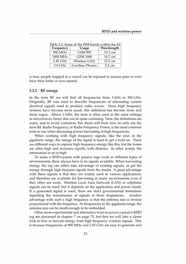
Table 3.2: Some of the ISM-bands within the EUFrequency Usage Wavelength900 MHz GSM 900 33.3 cm1800 MHz GSM 1800 16.7 cm2.45 GHz Wireless LAN 12.5 cm5.8 GHz Cordless Phones 5.2 cm
is true, people trapped in a crowd can be exposed to serious pain or evenhave their limbs or eyes injured.
3.2.3 RF energy
In the term RF we will find all frequencies from 3 kHz to 300 GHz.Originally, RF was used to describe frequencies of alternating currentelectrical signals used to produce radio waves. Since high frequencysystems have become more usual, this definition has become more andmore vague. Above 1 GHz, the term is often used in the same settingsas microwaves, hence this can be quite confusing. Now, the definitions aremany, and to avoid confusion, this thesis will from now on only use theterm RF. Radio Frequency, or Radio Frequency Power, is the most commonterm to use when discussing power harvesting at high frequencies.
When working with high frequency signals, like the ones in thegigahertz range, the energy of the signal is hard to get a hold on. Thereare different ways to capture high frequency energy like this, but the lossesare often high and increases rapidly with distance. In other words; theattenuation in air is high.
To make a RFID-system with passive tags work in different types ofenvironments, there always have to be signals available. When harvestingenergy, the tag can either take advantage of existing signals, or get theenergy through high frequent signals from the reader. A great advantagewith these signals is that they are widely used in various applications,and therefore are available for harvesting in many environments even ifthey often are weak. Wireless Local Area Network (LAN) or cellphonesignals can be used, but it depends on the application and power needs.If a generated signal is used, there are strict governmental limitationsregarding the transmission of signals at these frequencies. Anotheradvantage with such a high frequency is that the antenna size is inverseproportional with the frequency. At frequencies in the gigahertz range, theantenna size can be small enough to be embedded.
Other more experimental and alternative ways to power a passive RFIDtag are discussed in chapter 7 on page 73, but first we will take a closerlook at how to harvest energy from high frequency wireless signals. Thisis because frequencies of 900 MHz and 2.45 GHz are easy to generate and
23

RFID and wireless power
even can be found "naturally" around the tag.
24
RFID and wireless power
3.3 Frequency bands, calculations and measurements
First we will take a closer look at the 900 MHz and 2.4 GHz Industrial,Scientific and Medical (ISM) bands available for RFID use.
3.3.1 900 MHz ISM band
Around 900 MHz we find a popular frequency range for amateur radio,and in 1985 the “33 centimeter radio band” was born. The FederalCommunications Commission (FCC) allocated 902 MHz to 928 MHz forIndustrial, Scientific and Medical (ISM) devices. As part of that edict, theband was allocated to the Amateur Radio Service on a secondary basis.This means that hams can use the band as long as they accept interferencefrom and do not cause interference to the primary user. “Ham“ is aninformal term for an amateur radio operator, and the word "ham" wasborn in 1908 when the station call of the first amateur wireless stationwhere operated by amateurs of the Harvard Radio Club. They were namedHyman, Almy and Murray, and named their station by combining theircapital letters [Why 59].
5 years after the start, many mobile cordless phones appeared on thelower and upper ends of the 900 MHz band, phones that earlier operated at46 MHz. When this band became over-crowded, the phones moved up infrequency, and now do Global System for Mobile communications (GSM)mobile phones share this bandwith with automatic vehicle monitoringsystems and authorized U.S. governmental radio stations [ERC 04].
Unfortunately, this frequency band is not available for ISM applicationsin Europe at the moment, but outside Europe this band commonly used byRFID systems. The range of 868 MHz to 870 MHz is available in Europe forshort range devices like RFID, and is often used as a substitute [Fink 03].
3.3.2 2.4 GHz ISM band
The 2.4 GHz band covers frequencies from 2400 MHz to 2483.5 MHz and isbeing used for an increasingly diverse range of applications and systems.The band is non-licensed for private users, but is regulated with regardto power levels which leads to a potentially low level of service qualitywhen used in non-controlled environment with unpredictable levels ofinterference. This can be crucial to systems that are safety critical orpublic services where the quality have to be high at all times. Still the2.4 GHz band has many advantages. The low frequency, relative to othercommunication band like the 5.8 GHz band, makes the it suitable formobile communications. Another attraction is the global standardization,which makes it easier for international manufactures to design productsthat will work world wide.
25

RFID and wireless power
Table 3.3: Users of the 2.4 GHz ISM-bandUser type Exempt from license
Military NoElectronic News Gathering Noand Outside BroadcastPublic provision of Fixed Wireless Access NoRadio LANs YesBluetooth YesSoHo and Home networking YesRF Identification Devices YesVideo applications YesMicrowave ovens YesSulfur plasma lighting Yes
Table 3.4: The best known classes of the IEEE 802.11 standard
Standard Launched Medium ChannelsTheoreticalthroughput
802.11 1997 2.4 GHz 3 1-2 Mbps802.11b 1999 2.4 GHz 11(13) 11 Mbps802.11a 1999 5.6 GHz 12 54 Mbps802.11g 2003 2.4 GHz 11(13) 54 Mbps802.11n No 2.4 / 5 GHz 3 / 12 100-540 Mbps
The users of the 2.4 GHz band are many (See table 3.3). The militaryin several countries pays big money for use of this band every year, andmainly use it for communication and identification reasons [Lees 00]. TVstations and broadcast networks uses the band for short range transmissionof video. One example is coverage of sporting events, like transmissionof live picture from a field camera (following bikes, skiers, golfers etc.)to a central unit or a recorder. This is called Electronic News Gathering(ENG), which also covers on-site news reporting. ENG can be veryunpredictable in terms of timing and location and will in many cases haveto be established quickly, with little or no time for frequency co-ordinationand licensing. Other examples are Closed Circuit Television (CCTV), FixedWireless Access (FWA), Bluetooth and of course the IEEE 802.11 standard[Lees 00].
IEEE 802.11 is a set of standards for WLAN computer communication,developed by the IEEE LAN/MAN Standards Committee (IEEE 802). Thestandard includes both the 5 GHz and 2.4 GHz public spectrum bands,and is the one used by modern routers for wireless networks. The mostcommon classes of the IEEE 802.11 standard are listed in table 3.4, and theones used for WLAN are 802.11b and 802.11g.
26

RFID and wireless power
2.4GHz ISM band
2400 24502420 2430 24402410 2460 2470 2483.5
Military
SRD
AVI
Outside Broadcast Links
Radio Local Area Networks (Rec 7003)
Short Range Devices (Rec 7003)
2450
2455
2454
2445
2446
Figure 3.5: Users of the 2.4 GHz ISM-band. (Courtesy of Ægis SystemsLimited)
To get a estimate of how much available energy that can be carriedby a 2.45 GHz signal, and how much energy a passive wireless tag canharvest from it, a link budget is needed. In the calculation we use 2.45 GHz,because this is the center frequency of the ISM band. A link budget is theaccounting of all of the gains and losses from the transmitter, through amedium (in this case; air) to the receiver. The link budget takes into accountthe attenuation of the transmitted signal due to propagation as well as theloss, or gain, due to the antenna. This budget gives a good indicationalthough random attenuation such as fading is neglected.
3.3.3 Link Budget
A simple setup for received power:
ReceivedPower = TransmittedPower + Gains− Losses
To find all the gains and losses, both the transmitter antenna, the receiverantenna and all in between have to be included:
• RxP = received power ( dBm )
• TxP = transmitter output power ( dBm )
• TxG = transmitter antenna gain ( dBi )
27
RFID and wireless power
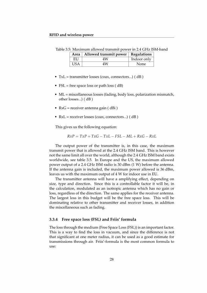
Table 3.5: Maximum allowed transmit power in 2.4 GHz ISM-bandArea Allowed transmit power RegulationsEU 4W Indoor only
USA 4W None
• TxL = transmitter losses (coax, connectors...) ( dB )
• FSL = free space loss or path loss ( dB)
• ML = miscellaneous losses (fading, body loss, polarization mismatch,other losses...) ( dB )
• RxG = receiver antenna gain ( dBi )
• RxL = receiver losses (coax, connectors...) ( dB )
This gives us the following equation:
RxP = TxP + TxG− TxL− FSL−ML + RxG− RxL
The output power of the transmitter is, in this case, the maximumtransmit power that is allowed at the 2.4 GHz ISM band. This is howevernot the same limit all over the world, although the 2.4 GHz ISM band existsworldwide, see table 3.5. In Europe and the US, the maximum allowedpower output of a 2.4 GHz ISM radio is 30 dBm (1 W) before the antenna.If the antenna gain is included, the maximum power allowed is 36 dBm,leaves us with the maximum output of 4 W for indoor use in EU.
The transmitter antenna will have a amplifying effect, depending onsize, type and direction. Since this is a controllable factor it will be, inthe calculation, modulated as an isotropic antenna which has no gain orloss, regardless of the direction. The same applies for the receiver antenna.The largest loss in this budget will be the free space loss. This will bedominating relative to other transmitter and receiver losses, in additionthe miscellaneous such as fading.
3.3.4 Free space loss (FSL) and Friis’ formula
The loss through the medium (Free Space Loss (FSL)) is an important factor.This is a way to find the loss in vacuum, and since the difference is notthat significant at one meter radius, it can be used as a good estimate fortransmissions through air. Friis’-formula is the most common formula touse:
28

RFID and wireless power
Friis’ formula:
FSL =(
4 · π · R · fc
)2
Since we modulate our antenna as an isotropic antenna, we can use amore simple form to calculate the loss with transmitter/receiver-distance r,and frequency f [Fink 03]:
FSL(dB) = 20 · log10(d) + 20 · log10( f )− 147.5 dB
If the relevant frequency (2.45 GHz) and radius (1 m) is inserted, theFSL will be:
FSL(dB) = 20 · log10(1) + 20 · log10(2.45 · 109)− 147.5 dB
FSL(dB) ' 40.3 dB
The figure 3.6 on the following page shows the FSL as a functionof frequency and radius as well as the specific losses for 900 MHz and2.45 GHz.
3.3.5 Calculation
RxP = TxP + TxG− TxL− FSL−ML + RxG− RxL
Receivedpower = 36 dBm− 40.3 dB
Receivedpower = -4.3 dBm
To convert dBm to watt we use the formula:
watt =1 mW · 10dBm
10
Then we get:1mW · 10
-4.3 dBm10 ' 0.35mW = 350µW
If a 50 Ω antenna is used:
P = V · I = V ·VR
=V2
R⇒
V =√
350 · 10−6W · 50Ω = 0.135 =135 mV
This result will vary with antenna gain and environmental variableslike humidity and reflections, but this estimate gives a good indication onhow much energy the tag can receive from WLAN signals. Chapter 5 onpage 41 describes how a CMOS charge pump can take advantage of thiseffect to create a supply voltage for a RFID tag.
29

RFID and wireless power
0 0.5 1 1.5 2 2.50
10
20
30
40
50
Distance (m)
Fre
e−sp
ace−
loss
(dB
)
900 MHz2.45 GHz
(a) FSL as a function of distance at 900 MHz and 2.45 GHz
(b) FSL as a function of distance and frequency
Figure 3.6: Free space loss
30

RFID and wireless power
Figure 3.7: Antennas used in the measurements at 1 and 2.45 GHz
From literature on the subject (i.e. [Zhou 03]), we can read that wirelesstags often receive up to 100 µW, and AC inputs of around 100 mV. Tocompare the theoretical estimate with the reality, a test with real antennasand transmissions was preformed. A signal generator with ability togenerate high frequencies was used with an antenna to broadcast a signalwith a certain amplitude and frequency. At the receiver antenna the signalwas logged by an oscilloscope. Three different types of antennas whereused; monopol bowtie, dipole bowtie and 25 cm loop antenna as shown infigure 3.7.
Various frequencies and energies where transmitted and measured atdifferent ranges. When sending 1 V amplitude through the antenna atboth 1 GHz and 2.45 GHz, up to 500 mV was received at the secondantenna when the distance was a few centimeters. At longer ranges, upto 1 m, the received signal had a maximum of 100 mV. Altough this wasnot performed with antennas made exactly for these frequencies and thispurpose, it shows that it is possible to receive signals in the hundreds ofmillivolt scale at these frequencies. It is not an easy task to use air as aconductor, as described in chapter 3.3.4, but still these signals are strongenough to make use of in a wireless scenario. To better understand whatthe purpose of the prospective power harvest is, we will now review sometransmission methods commonly used in wireless communication.
31

RFID and wireless power
32

Chapter 4
Transmission of data
To understand wireless communication technologies like RFID, we alsohave to understand the last step of the system, the transmission of the ID.The transmission of the data from the tag to the receiver is a crucial partof the system, because the power and space restrictions of the tag makethe process quite complex. In addition to these requirements, the coding ofthe unique identification code of each tag is important to make the systemwork with several tags simultaneously. There are different ways to transmitsignals from a chip, and some of the most common principles are describedin this chapter, together with a comparison of these.
4.1 Analog modulation, AM and FM
The traditional way of transmitting a signal in a wireless manner isto modulate the signal on a carrier frequency. This is used in radio-communication since early 1900, and the signal is either modulatedby amplitude (Amplitude Modulation (AM)) or frequency variations(Frequency Modulation (FM)). The first form of amplitude modulationwas introduced in the mid-1870s under the name "undulatory currents",but not used in a practical way for radio communications before ReginaldFessenden demonstrated the AM transmission we know today early inthe 1900’s [Raby 70]. AM transmissions consist of a carrier with a certainfrequency and a signal to be transmitted. Mixed together the resultant isa signal varying in amplitude according to the signal we want to transmit.This is an intuitive and easy implementation, but not very power effective.Much of the power is used in the carrier signal and this signal does notconsist any information. An important consideration is the bandwidth,which here is the range of frequencies around the carrier frequency. Asan example, an AM radio station has only 10kHz of bandwidth, with thecarrier frequency in the center of the range. To use AM to transmit musicis therefore not preferred as the musical range of the human ear is about 20
33

Transmission of data
kHz, which is about twice the bandwidth of a standard AM transmission.FM, on the other hand, is a bit younger method invented by Edwin
Armstrong in 1935 [Arms 36]. In commercial radio broadcasting all overthe world, frequency modulation is the standard way of transmittingsignals. This is, as the name indicates, a modulation of the frequencyrather than the amplitude, as in AM. The FM requires a wider bandwidththan amplitude modulation making it more suited for sound transmission.This larger bandwidth also makes the signal more robust regardingnoise, interference and simple signal amplitude fading phenomena. Thebandwidth of FM radio stations are around 200kHz, with the carrierfrequency in the middle. The principles behind AM and FM are shownin figure 4.1.
Figure 4.1: AM and FM modulation. (Courtesy of Wikipedia)
These modulation techniques described above are both analogue, henceboth the transmitted signal and the carrier are analog signals. This is notpreferable in passive RFID-tags because when generating an analog signal,an oscillator is needed. This can be implemented in active tags, but analogmodulation of the signal is not commonly used. In most tags, digitalmodulation is the most common way to make a unique id.
4.2 Digital modulation, ASK and PSK
When the modulation of a signal is digital, the technique is basically ananalog-to-digital conversion. An analog carrier signal is modulated bya digital bit stream. This bit-stream can be either of equal or varyinglength signals, and this modulation works much like an Analog to DigitalConverter (ADC). The simplest form of digital modulation is Morse code,invented by Samuel F. B. Morse and Alfred Vail in the beginning in the1830’s [Mors 08]. This is a well known transmission method and consistsof pauses, long and short pulses. This is much similar to the modern "bit",
34

Transmission of data
and in many ways we can say that Morse-code is the predecessor to thedigital bit. In modern RFID technology, digital modulation is the preferredway to transmit signals. Amplitude, frequency and phase shift keying is allused in RFID tags today, also in passive tags.
Figure 4.2: Digital modulation, ASK, PSK and FSK (Courtesy of NakagawaLabs.)
ASK is the digital part of AM. A carrier signal is modulated by abit-stream, keeping the frequency and phase constant. The differentamplitude-levels is then representing 0’s and 1’s. An advantage withASK is simplicity, and the modulation and demodulation is therefore quiteinexpensive. The main drawbacks is that, in similarity with AM, ASKis a linear technique with high sensitivity to noise and distortions. Toreduce the effect of the noise, the frequency can be modulated insteadof the amplitude. This is called Frequency Shift Keying (FSK). With thismethod the signal shifts the output frequency between predeterminedvalues. This was the common way to transfer signals in early telephone-line modems, which used the audio frequency-shift keying with rates upto about 300 bits per second. This is a modulation where digital datais represented in the frequency of an audio-tone, making is suitable fortransmission via telephone or radio. The transmission has two states ortones, a mark which represent the binary one, and a space which representsthe zero. This audio-modulated technique is not appropriate for high-speed communication, because it is not very efficient regarding power andbandwidth compared to other techniques. The advantages on the otherhand, is simplicity and possibility to pass encoded signals through ACcoupled links, including most equipment designed for music or speech.
35

Transmission of data
The principles behind ASK, PSK and FSK are shown in figure 4.2 on thepreceding page.
When designing a RFID system, it is important to choose the suitabletransmission method. As we have seen, have all the techniques discussedabove both advantages and drawbacks. A transmission technologydemanding an on-chip oscillator will not be practical implementable ina passive wireless solution. This is because of the power required torun the oscillator will dominate, and the power demand of the tag willexceed the amount of air-born power available. Some of the transmissiontechniques can take advantage of the possibility to scatter the signal back,but this will also imply a more complex tag than necessary. To make thistransmission power effective and simple, an impulse transmission alsohave to be considered.
4.3 UWB-IR
The conventional communication systems transmit information by varyingthe power, the frequency and/or the phase of a sinusoidal wave. ImpulseRadio (IR) broadcasts by generating pulses where the information ismodulated on the pulses by encoding the polarity, time spacing, amplitude,and/or by using orthogonal pulses [Bene 04]. Since the pulses are veryshort in time, they occupy a very large bandwidth, hence Ultra Wide Band(UWB). The transmission of pulses can either be sent sporadically at lowpulse rates to support time/position modulation, or sent at rates up to theinverse of the UWB pulse bandwidth. The "FCC power spectral densityemission limit" for the UWB band is -41.3 dBm/MHz. This is the same limitthat applies for unintentional signals in the band, and therefore will thetransmission strength be close to the noise in the band, see figure 4.3(a) onthe next page. Since the strength is close to other unintentional signalsand noise, this technique depends on repetition to succeed. Transmittingone unique train of pulses may not be recognizable, but repeating thesequence several times will make the sequence distinguishable from thenoise. Because of this property, UWB-IR it is a viable candidate for short-range communications in dense multipath environments where the S/R-ratio (signal-to-noise) can be quite significant.
The properties of impulse radio transmission in the UWB band is, as wecan see, suitable in order to transmit from an RFID tag with the specs givenin this thesis. To transmit using impulse radio technology, an embeddedpulse generator is required. A low-power pulse generator like this willnot be discussed in this thesis, for further reading please see [Mars 03] or[Moen 06].
There are systems that do not use any complex pulse coding at all, andare truly passive. To review one example of this we will know take a closer
36

Transmission of data
(a)
(b)
Figure 4.3: The UWB compared to other frequency bands (Courtesy ofInstitute for Integrated Signal Processing Systems)
37

Transmission of data
look at SAW filters.
4.4 Surface Acoustic Wave filters (SAW filters)
Surface acoustic wave mode of propagation was first discovered by LordRayleigh, and the properties of these waves were reported in his paperfrom 1885 [Stru 85]. Lord Rayleigh, born John William Strutt, 3rd BaronRayleigh, gave names to these waves, and today these are known as“Rayleigh waves”. Rayleigh waves have both vertical and longitudinalcomponents, which couples with the medium when they make contactwith the surface of the device. This coupling affects the wave, and theamplitude and velocity will then change according to the characteristics ofthe material.
Figure 4.4: A Surface Acoustic Wave filter on a piezoelectric substrate. (ITFCo., Ltd.)
Lord Rayleigh, who got the Nobel Prize for Physics in 1904 due tohis discovery of Argon, also discovered the foundation for SAW filterswith his Rayleigh waves. These kind of filters are used in differentidentification systems, and was in the 1980’s and 90’s widely used intoll roads, i.e. in Oslo, Norway. The principles behind SAW filters aresimple; the input signal is converted to a sound wave by a transducer,which creates a mechanical pressure in the material. This material, whichis a piezoelectric material, then generates waves. These waves propagatealong the surface of the material to a second transducer, which detects thefrequency components of interest and convert these to electric current. Theoutput of the filter is then “coded“ with the characteristics of the material,and can be used to identify that specific tag.
The advantages with this kind of filter identification is that they havehigh tolerance to mechanical noise, temperature changes and movements,a high Q-factor and low production costs. Compared to silicon based RFID
38

Transmission of data
is this a cheaper and simpler technology, but the SAW filter has somedrawbacks. The filters have low efficiency, the output is quite dampedcompared to the input. This can of course be corrected with an amplifier,but amplifiers need a supply voltage, which again will make the RFIDenergy harvesting even harder. The SAW filters were replaced by semi-active silicon based RFID tags in the late 90’s, because the semi-activesilicon based tags had longer range and were more suitable for packingand sealing, making the tag more resistant to environmental strains.
No matter which kind of coding and transmission used, the tag stillneed energy. To power any type of tag with microwaves, RF energy orinduction, an important part on the tag will be the energy harvesting. Inthe following chapters different energy sources will be discussed, as wellas the different techniques of how to take advantage of them in order totransmit the tag’s data.
39

Transmission of data
40

Chapter 5
Voltage boosting
From the result of the link budget in chapter 3.3.3 on page 27, we can seethat the calculated input voltage is far too low to power the tag. To generatea suitable supply voltage from the WLAN-signals, boosting and rectifyingis needed. The typical supply voltage in a 90 nm process is around 1 V, andto achieve this the input voltage has to be multiplied by 10. On the otherhand, a voltage below this value can be sufficient, but will depend on thesystem.
There are several ways to generate this supply voltage from thealternating input voltage, and some of these methods will now bediscussed.
RFin Chargepump DCsupplyvoltage
Figure 5.1: The input stage of a charge pump RFID-tag.
5.1 Boost and Buck converters
Boost and buck converters are technologies developed in the early 1960’swhen switches made from semiconductors become commercially available.One of the main motivations for this development was the aerospaceindustry that needed small, efficient and lightweight power converters inhigh numbers. Buck converters is used to scale down voltages and are notinteresting under this topic. The boost converter technology on the otherhand, is a type of circuit worth looking into.
41

Voltage boosting
Figure 5.2: A conventional boost converter
The basic principle of a boost converter can be divided into two distinctstates, the ON- and OFF-state, as shown in figure 5.3 on the next page. Atthe ON-state, the switch is closed and there will be an increasing currentin the inductor. At the Off-state, the switch is open and the current fromthe inductor will have to flow through the diode and the capacitor C. Afterthis state, the energy accumulated during the ON-state is transfered to thecapacitor, resulting in a higher output than input voltage.
If we start by looking at blue path in figure 5.3 on the facing page, wecan see that the switch is on(closed) and Vx = Vin. At the off-state theinductor current flows through the diode giving Vx = Vo. This is correct ifwe assume that the inductor current flows continuously and the diode isideal. The average voltage across the inductor must be zero for the averagecurrent to remain in steady state.
Vin · ton + (Vin + Vo) · to f f = 0
Vo
Vin=
ton + to f f
to f f=
Tto f f
=1
1− D
where T = ton + to f f and D = tonT is defined as the duty ratio for the
converter without losses. If the duty ratio, D, is between 0 and 1 will theoutput voltage be higher than the input voltage in magnitude, and this willalways be the case for boost converters.
The boost converter can be useful for a RFID application, but if used,the input voltage to the tag have to be rectified because the boost converteris a DC to DC converter. To illustrate this, a boost converter just like theone in figure 5.2 is simulated for 2.5 ms with an inductor value of 500 µH,200 mV DC input and a switch transistor with a pulse period of 50 µs. Thecircuit is simulated with 100 kΩ, 200 kΩ, 500 kΩ, 1 MΩ and 2 MΩ load.As we can see from figure 5.4 on the facing page, the volage boosting isconsiderably, at least with high resistance loads. This is because the outputcurrent will change in relation to the load and change the voltage accordingto Ohm’s law; U = R · I.
42

Voltage boosting
Figure 5.3: The states of a boost converter
0 0.5 1 1.5 2 2.50
0.2
0.4
0.6
0.8
1
1.2
1.4
Time (ms)
Vol
tage
(V
)
100kΩ200kΩ500kΩ1MΩ2MΩInput
Figure 5.4: Input and output of a boost converter with different loads.
43

Voltage boosting
The use of boost converters with RFID is further discussed in chapter5.7.
5.2 Charge pumps
Another method for raising a input voltage to a higher voltage level at theoutput, is by pumping charge by the use of a charge pump.
5.2.1 The Dickson charge pump
The charge pump technology is old, and one of the first and most basicversion is the Dickson charge pump from 1976 [Dick 76], see figure 5.5.Most charge pumps use an AC input to generate a DC output voltage, andtherefore also work as rectifiers.
φ2
φ1
VOut
C
CS
Vin
Figure 5.5: The mother of all charge pumps: The Dickson
This type of charge pump consists of two pumping clocks, φ1 and φ2,in opposite phase. The clock signals have a voltage Vφ, and the diodeswork as switches. The Dickson operates by pumping the charge throughthe diodes, and charges the capacitors each clock cycle. Each step will addVφ to the chain, but there will be a voltage drop at each diode, VD. After Nstages, a simple form of the output voltage can be written as:
VOut = Vin + N · (Vφ −VD)−VD
There will be an extra VD at the end of the equation because it is one morediode than steps in the pump.
The Dickson is a good choice for many applications, but in this case notoptimal. Since an on-chip clock-generator requires both space and power,the Dickson charge pump is not a preferred solution for not only passiveRFID tag, but for RFID generally. In a RFID case the input signal can beused as a shifting clocks, but is not preferred as the input signal typically isquite small and sometimes unstable. To avoid the need of clock-signals, acascode charge pump is a far better alternative. This type of pump uses the
44
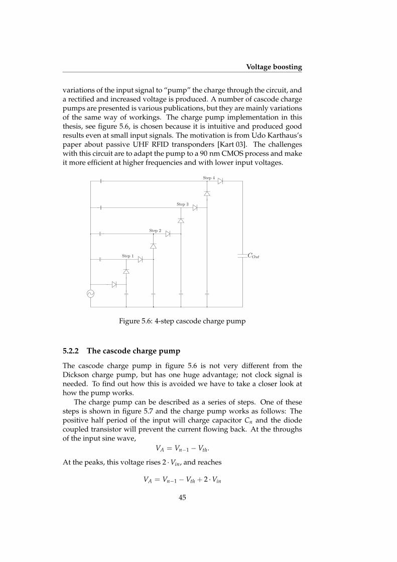
Voltage boosting
variations of the input signal to “pump” the charge through the circuit, anda rectified and increased voltage is produced. A number of cascode chargepumps are presented is various publications, but they are mainly variationsof the same way of workings. The charge pump implementation in thisthesis, see figure 5.6, is chosen because it is intuitive and produced goodresults even at small input signals. The motivation is from Udo Karthaus’spaper about passive UHF RFID transponders [Kart 03]. The challengeswith this circuit are to adapt the pump to a 90 nm CMOS process and makeit more efficient at higher frequencies and with lower input voltages.
COutStep 1
Step 2
Step 3
Step 4
Figure 5.6: 4-step cascode charge pump
5.2.2 The cascode charge pump
The cascode charge pump in figure 5.6 is not very different from theDickson charge pump, but has one huge advantage; not clock signal isneeded. To find out how this is avoided we have to take a closer look athow the pump works.
The charge pump can be described as a series of steps. One of thesesteps is shown in figure 5.7 and the charge pump works as follows: Thepositive half period of the input will charge capacitor Cn and the diodecoupled transistor will prevent the current flowing back. At the throughsof the input sine wave,
VA = Vn−1 −Vth.
At the peaks, this voltage rises 2 · Vin, and reaches
VA = Vn−1 −Vth + 2 · Vin
45

Voltage boosting
Cn will be charged to VA −Vt:
Vn = Vn−1 + 2 · Vin − 2 · Vth (5.1)
Each step of the charge pump can not increase the pumped voltagemore than two times the amplitude of the input voltage minus two timesthe threshold voltage of the transistors. If the low-threshold models in the90 nm technology are used, the diode threshold voltage will be 0.18 V. Thismeans that, with no modifications to the circuit, the input amplitude mustexceed 0.18 V to get the charge pump to pump voltage through the stepstowards the last capacitor. With the backgate connection proposed later inthis chapter, the charge pump can work at even lower inputs. We have tokeep in mind that the equation above regards a charge pump with idealdiodes, and can be considered a good approximation. A more practicalanalysis will follow later in this chapter, in equation 5.2 on page 52.
CC
Vn
A
Vn−1
Mna
CnVin
Mnb
Figure 5.7: One step of the charge pump
To maximize the output voltage in this circuit, there are two mainfactors; minimize the threshold voltage or increase the number of steps.Since increasing the number of steps will cause degradation of power andconversion efficiency and also increased circuit size, lowering the voltagedrop of the transistors is the most efficient way to improve the chargepump.
If we take a look at the threshold voltage of a transistor in the trioderegion [John 97], we can see the relationship between the transistor currentand W/L.
Ids = β ·
((VGS −Vt) · VDS −
V2DS2
)
β = µn · Cox ·WL
To ensure pumping at low input voltages we will need a low Vth, andto ensure that we are able to deliver as much current as possible, W/L and
46
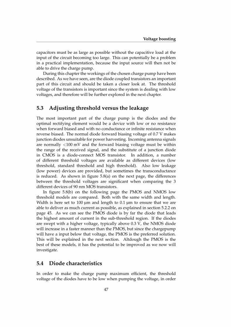
Voltage boosting
capacitors must be as large as possible without the capacitive load at theinput of the circuit becoming too large. This can potentially be a problemin a practical implementation, because the input source will then not beable to drive the charge pump.
During this chapter the workings of the chosen charge pump have beendescribed. As we have seen, are the diode coupled transistors an importantpart of this circuit and should be taken a closer look at. The thresholdvoltage of the transistors is important since the system is dealing with lowvoltages, and therefore will be further explored in the next chapter.
5.3 Adjusting threshold versus the leakage
The most important part of the charge pump is the diodes and theoptimal rectifying element would be a device with low or no resistancewhen forward biased and with no conductance or infinite resistance whenreverse biased. The normal diode forward biasing voltage of 0.7 V makesjunction diodes unsuitable for power harvesting. Incoming antenna signalsare normally <100 mV and the forward biasing voltage must be withinthe range of the received signal, and the substitute of a junction diodein CMOS is a diode-connect MOS transistor. In addition, a numberof different threshold voltages are available as different devices (lowthreshold, standard threshold and high threshold). Also low leakage(low power) devices are provided, but sometimes the transconductanceis reduced. As shown in figure 5.8(a) on the next page, the differencesbetween the threshold voltages are significant when comparing the 3different devices of 90 nm MOS transistors.
In figure 5.8(b) on the following page the PMOS and NMOS lowthreshold models are compared. Both with the same width and length.Width is here set to 100 µm and length to 0.1 µm to ensure that we areable to deliver as much current as possible, as explained in section 5.2.2 onpage 45. As we can see the PMOS diode is by far the diode that leadsthe highest amount of current in the sub-threshold region. If the diodesare swept with a higher voltage, typically above 0.3 V, the NMOS diodewill increase in a faster manner than the PMOS, but since the chargepumpwill have a input below that voltage, the PMOS is the preferred solution.This will be explained in the next section. Altdough the PMOS is thebest of these models, it has the potential to be improved as we now willinvestigate.
5.4 Diode characteristics
In order to make the charge pump maximum efficient, the thresholdvoltage of the diodes have to be low when pumping the voltage, in order
47

Voltage boosting
0 0.1 0.2 0.3 0.40
0.05
0.1
0.15
0.2
0.25
0.3
0.35
0.4
Voltage (V)
Cur
rent
(µA
)
High threshold modelStandard threshold modelLow threshold model
(a) Diode coupled MOS transistors. Simulated with minimum sizes.
−0.2 −0.1 0 0.1 0.20
100
200
300
400
500
600
700
800
Voltage (V)
Cur
rent
(µA
)
NMOS low threshold modelPMOS low threshold model
(b) Low threshold models of PMOS and NMOS.
Figure 5.8: Comparison of different MOS models
48
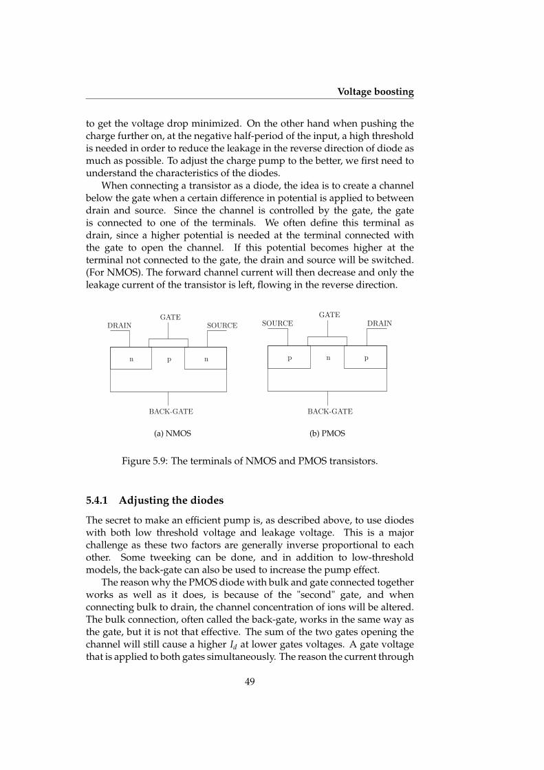
Voltage boosting
to get the voltage drop minimized. On the other hand when pushing thecharge further on, at the negative half-period of the input, a high thresholdis needed in order to reduce the leakage in the reverse direction of diode asmuch as possible. To adjust the charge pump to the better, we first need tounderstand the characteristics of the diodes.
When connecting a transistor as a diode, the idea is to create a channelbelow the gate when a certain difference in potential is applied to betweendrain and source. Since the channel is controlled by the gate, the gateis connected to one of the terminals. We often define this terminal asdrain, since a higher potential is needed at the terminal connected withthe gate to open the channel. If this potential becomes higher at theterminal not connected to the gate, the drain and source will be switched.(For NMOS). The forward channel current will then decrease and only theleakage current of the transistor is left, flowing in the reverse direction.
BACK-GATE
GATE
n p n
SOURCEDRAIN
(a) NMOS
pp n
BACK-GATE
GATESOURCE DRAIN
(b) PMOS
Figure 5.9: The terminals of NMOS and PMOS transistors.
5.4.1 Adjusting the diodes
The secret to make an efficient pump is, as described above, to use diodeswith both low threshold voltage and leakage voltage. This is a majorchallenge as these two factors are generally inverse proportional to eachother. Some tweeking can be done, and in addition to low-thresholdmodels, the back-gate can also be used to increase the pump effect.
The reason why the PMOS diode with bulk and gate connected togetherworks as well as it does, is because of the "second" gate, and whenconnecting bulk to drain, the channel concentration of ions will be altered.The bulk connection, often called the back-gate, works in the same way asthe gate, but it is not that effective. The sum of the two gates opening thechannel will still cause a higher Id at lower gates voltages. A gate voltagethat is applied to both gates simultaneously. The reason the current through
49

Voltage boosting
the PMOS transistor is increasing at a lower voltage than the NMOS, is thelevel of doping and threshold voltage. The doping of the PMOS well ishigher than the doping of the NMOS substrate, because of the increasedmobility of the NMOS. This will lower the threshold, hence increase thecurrent at lower voltages.
The threshold voltage can be expressed [John 97] like
Vth = VtO + γ
(√Vsb + |2φF| −
√|2φF|
)where γ is the body-effect parameter, 2φF is the surface potential, and Vthis the zero bias threshold voltage.
As we can see from the equation above, the Vsb is a parameter that canbe altered to achieve a low Vth. The back-gate connection can be describedas a change in the bulk potential, hence causing a reversed body-effect. Thebody-effect is an effect describing changes in the threshold voltage of thetransistor by the change in the source-bulk voltage, Vsb. Even these diodeswill operate in a subthreshold area, the working way of the transistorswill be the same. In subthreshold operation, this is even more important.To investigate this factor, the diode current is simulated as a function ofvoltage.
−0.4 −0.2 0 0.2 0.4−1
0
1
2
3
4
5
6
Voltage (V)
Cur
rent
(µA
)
Back gate and gate connectedConventional back gate connection
Figure 5.10: A diode connected PMOS transistor (low threshold model)compared to one with gate and backgate connected. Simulated withminimum sizes.
In the following simulations the test bench is swept with a voltage from
50

Voltage boosting
-0.4 V to 0.4 V, which will be more than sufficient range compared to theinput AC of the actual circuit. During the sweep, the diode current ismeasured for different types of diodes and the prospective aberration isshown. The meaning of this study is to see which diode that has the bestratio between current at low voltages in forward direction and the leakagein the backward direction. It is important to choose a solution that has ahigher exponential growth regarding current above, than below 0 V. Thisis important because this difference creates the pumping effect in the chargepump.
−1
0
1
0
0.2
0.410
−10
10−5
100
Offset(V)Amplitude(V)
Abs
olut
e av
erag
e di
ode
curr
ent (
A)
Figure 5.11: PMOS diode characteristics - The diode current as a functionof offset and amplitude.
The diodes in the charge pump will be operating on a AC signalwith amplitude of approximately 100 mV, but the signal will not alwaysalternate around ground level. With time, each step will build an offset.This is because Cn will be charged until the forward diode current andthe leakage is equal, when the average current through the diode is zero.In figure 5.11 the diode current is simulated as a function of offset andamplitude across the diode. Here, the diode current is interpolated witha generated sinusoidal with a given offset and amplitude. The offset isan important factor since it is the offset that will charge each step, togetherwith the amplitude. This will give us important information regarding howthe diodes will behave with time, and where the stabilization point of thediodes are.
51

Voltage boosting
The most important info from figure 5.11 on the page before is thatthe stabilization point of the diode, where the average current is zero, isbelow zero offset. This means that Cn can be charged with the differencefrom the stabilization point to zero offset. This can be seen even clearer onfigure 5.12 on the facing page that shows the offset with fixed amplitudesfor both low and standard threshold transistor models. Here we can seethat the pump effect will increase considerable with higher amplitude. Allthis is because of the exponential growth of the diode current. It is theabsolute value of the diode current that is shown in figure 5.12 on the nextpage. This means that the minimum, the dip, of each plot is the point wherethe current drops below zero, and switches direction. The reason why thisminimum is not closer to the negative infinity, which will be zero on a logscale, is because of the resolution of the plotted data. Still, this minimumis easy to see, even at the 100 mV plots. Figure 5.12(e) shows that with a100 mV input amplitude, the stabilization point of the diode will be around75 mV. If we again look at 5.7 on page 46, we can now express the outputvoltage of each step as a function of the offset of each diode:
Vn = Vn−1 + 2 · Vstabile (5.2)
where, Vstable is the stabilization of the offset in the two diodes.Figure 5.12 also shows a soft-well PMOS transistor. This is a coupling
that will increase the potential of the back-gate of the transistor, altering thebody-effect. Not commonly used, but gave promising results, altdough notbetter than the PMOS with gate and back-gate connected. (It is hard to seethe difference in figure 5.12, but the back-gate connected PMOS is slightlybetter than the soft-well PMOS.)
In the charge pump layout, presented later in this chapter, the pumpare designed with PMOS diodes with back-gate connection as described inthis chapter, and the high W
L relationship. This is as we have seen, to ensureimproved pump effect.
5.5 Capacitors
The choice of capacitors to use with the charge pump is important as theseare responsible for storing the charge at each step of the pump, as wellas DC block the input from the accumulated charge. One huge problem,litterally speaking, with capacitors in a CMOS process is the size. Largecapacitors demands large area, and with limited space on a chip, embeddedcapacitors are a challenge.
The space available on the chip that will be sent to production, is 300 µmx 200 µm. To meet the requirements of size and value, various capacitorswere simulated and tested in the circuit. A solution to the problem withlarge areas, is placing the capacitors off-chip and connect them via pins,
52

Voltage boosting
−0.2 −0.1 0 0.1 0.210
−10
10−8
10−6
10−4
10−2
Offset (V)
Dio
de C
urre
nt (
A)
PMOSNMOS gate−bulk connectionPMOS gate−bulk connectionPMOS soft−well
(a) 20 mV amplitude.
−0.2 −0.1 0 0.1 0.210
−10
10−8
10−6
10−4
Offset (V)ab
s(D
iode
Cur
rent
) (A
)
PMOSNMOS gate−bulk connectionPMOS gate−bulk connectionPMOS soft−well
(b) 20 mV amplitude.
−0.2 −0.1 0 0.1 0.210
−8
10−7
10−6
10−5
10−4
10−3
Offset (V)
abs(
Dio
de C
urre
nt)
(A)
PMOSNMOS gate−bulk connectionPMOS gate−bulk connectionPMOS soft−well
(c) 50 mV amplitude.
−0.2 −0.1 0 0.1 0.210
−10
10−8
10−6
10−4
Offset (V)
abs(
Dio
de C
urre
nt)
(A)
PMOSNMOS gate−bulk connectionPMOS gate−bulk connectionPMOS soft−well
(d) 50 mV amplitude.
−0.2 −0.1 0 0.1 0.210
−8
10−7
10−6
10−5
10−4
10−3
Offset (V)
abs(
Dio
de C
urre
nt)
(A)
PMOSNMOS gate−bulk connectionPMOS gate−bulk connectionPMOS soft−well
(e) 100 mV amplitude.
−0.2 −0.1 0 0.1 0.210
−10
10−8
10−6
10−4
10−2
Offset (V)
abs(
Dio
de C
urre
nt)
(A)
PMOSNMOS gate−bulk connectionPMOS gate−bulk connectionPMOS soft−well
(f) 100 mV amplitude.
Figure 5.12: The diode current as a function of offset with fixed amplitudes.Low threshold models on the left, standard threshold models on the right.
53

Voltage boosting
Table 5.1: Capacitors in a STM 90nm CMOS processType fF
µm2 DescriptionFringe 1.2 Capacitor with "fingers"MIM 2 Metal-Insulator-Metal
P-poly 5-15 Cap. between poly and p-wellpMOS 5-15 Cgs + Cgb + Cgd
but with this arrangement the inevitable capacitance of the pins will comeinto play, especially with RF signals In addition, it is the impractical part ofhaving discrete components outside the chip. Some of the capacitors in the90 nm design kit have large enough capacitance per area, but these are notlinear with the voltage. Since off-chip capacitors are impractical and willaffect the RF signal, the non-linear on-chip capacitors are the most optimalchoice. As we can see from figure 5.14 on the next page, the output ofthe circuit is not that much affected by changes in the capacitor value, andnonlinearity will not be much of a problem even with the variation shownin figure 5.13.
Figure 5.13: A CMOS transistor used as a capacitor is nonlinear regardingoperating voltage.
The change of the charge pump output voltage due to capacitorvariations is dependent of the time pumped. As figure 5.14 on the facingpage shows, the smallest capacitance increases the most from time 0, but
54
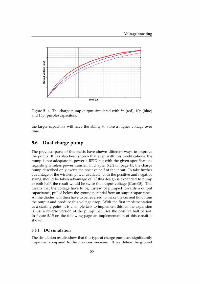
Voltage boosting
Time (us)
Ou
tpu
t vo
ltag
e (m
V)
2.5 5 7.5 10 12.5 15
250
200
150
100
50
0
Figure 5.14: The charge pump output simulated with 5p (red), 10p (blue)and 15p (purple) capacitors.
the larger capacitors will have the ability to store a higher voltage overtime.
5.6 Dual charge pump
The previous parts of this thesis have shown different ways to improvethe pump. It has also been shown that even with this modifications, thepump is not adequate to power a RFID-tag with the given specificationsregarding wireless power transfer. In chapter 5.2.2 on page 45, the chargepump described only exerts the positive half of the input. To take furtheradvantage of the wireless power available, both the positive and negativeswing should be taken advantage of. If this design is expanded to pumpat both half, the result would be twice the output voltage [Curt 05]. Thismeans that the voltage have to be, instead of pumped towards a outputcapacitance, pulled below the ground potential from an output capacitance.All the diodes will then have to be reversed to make the current flow fromthe output and produce this voltage drop. With the first implementationas a starting point, it is a simple task to implement this, as the expansionis just a reverse version of the pump that uses the positive half period.In figure 5.15 on the following page an implementation of this circuit isshown.
5.6.1 DC simulation
The simulation results show that this type of charge pump are significantlyimproved compared to the previous versions. If we define the ground
55

Voltage boosting
Step 2
Step 3
Step 4
Step 1
Step 2
Step 3
Step 4
Step 1 COut+
COut−
VOut−
VOut+
Figure 5.15: Charge pump that exploit both positive and negative halfperiods
56

Voltage boosting
Figure 5.16: Testbench used to simulate the charge pump
potential as the negative output, a supply voltage up to 600 mV is available.This with just around 100 mV AC input swing to the charge pump. Tomake the circuit simulation more close to reality, a serial input resistanceof 50 Ω is used to represent the resistance of the antenna. A outputresistance of 1 MΩ at both at the positive and negative output is used inthe simulations to represent a transmitter with high impedance attached tothe charge pump, using the supply voltage generated. See figure 5.16.
As we can see from the results, is the performance of the circuit bothdependent of the load and frequency. Frequencies in the gigahertz rangegenerate a lower output voltage than in the megahertz range, due tocapacitive losses. It is worth noticing that input signals with very lowfrequency will also result in a lower output voltage, since the input thenis not alternating fast enough and the leakage in the transistors will depletethe charge between each cycle.
5.6.2 AC simulation
To find out how much of the RF signal that is left at the output of the chargepump, a AC simulation i performed. This is done by simulating the pumpwith a DC block capacitor at the output. As we can see in figure 5.18 onpage 59, some of the AC input signal is left at the output, but this is below5 mV and will not be a problem, since the DC is relative so much larger.
5.6.3 Process variations
To find out if the charge pump will be significantly affected by variationsin the manufacturing process, the circuit is simulated with a Monte Carlosimulation. This will simulate the charge pump running several times, butwith different sizes and values of the components. These changes representthe variations that can occur from one process to another or within the
57

Voltage boosting
0 5 10 15 20 25 30 35 40−0.5
−0.4
−0.3
−0.2
−0.1
0
0.1
0.2
0.3
0.4
0.5
Time (µs)
Out
put v
olta
ge (
V)
50 Ω generator and 2MΩ loadIdeal generator and no load
(a) 900 MHz
0 5 10 15 20 25 30 35 40−0.5
−0.4
−0.3
−0.2
−0.1
0
0.1
0.2
0.3
0.4
0.5
Time (µs)
Out
put v
olta
ge (
V)
50 Ω generator and 2MΩ loadIdeal generator and no load
(b) 2.45 GHz
Figure 5.17: Time development of charge pump output
58

Voltage boosting
0 0.5 1 1.5 2−4
−3
−2
−1
0
1
2
3
4
Time (ns)
Out
put v
olta
ge (
mV
)
Positive output − V+Negative output − V−
(a) 900 MHz
0 0.2 0.4 0.6 0.8 1−4
−3
−2
−1
0
1
2
3
4
Time (ns)
Out
put v
olta
ge (
mV
)
Positive output − V+Negative output − V−
(b) 2.45 GHz
Figure 5.18: The AC component of the output voltage
59

Voltage boosting
same process. As we can see from figure 5.19, the variation in the output
250 251 252 253 254 255 256 2570
10
20
30
40
50
Voltage (mV)
Dis
trib
utio
n(%
)
(a) Schematic
26 27 28 29 300
5
10
15
20
Voltage (mV)
Dis
trib
utio
n(%
)
(b) Layout
Figure 5.19: The changes in the circuit due to process variations.
due to the process variations is quite small. The standard deviation is wellbelow 1 mV, when the output is about 250 mV. The circuits should behavein almost an identical manner, even from one “extreme” to another. Thenumber of runs should ideally been higher, but this was not possible dueto time and storage restrictions at the workstation where the simulationwas preformed. The layout of the charge pump is simulated just a tenth ofthe time the schematic is, due to the same restrictions. Results of the MonteCarlo simulation are shown i table 5.2, where µ is the arithmetic mean, σ isthe standard deviation and N is the number of runs.
Table 5.2: Monte Carlo simulationSchematic Layout
µ 253.30 mV 28.35 mVσ 521.49 µV 359.28 µVN 125 125
5.6.4 Layout of the charge pump
In figure A.1 on page 93, the layout of the the circuit is shown. Theinput capacitors are the large blocks on the left side, and the blocks on theright side are the capacitors connected to ground. The layout is arrangedthis way to separate the RF input on the left from ground, and this wayminimize the capacitance directly from input to ground. Between thesecapacitor blocks, the transistors are placed, with the first steps of the pumpin the center. The positive and negative output of the pump are placedtop center and bottom center respectively, and ground is connected at the
60

Voltage boosting
right side of the circuit. The size of the layout is 260 µm x 160 µm, and alsoinclude outputs within the pump for measuring purposes during testing.Measurements of the chip are shown in chapter 6 on page 63.
5.7 Boostconverting of the charge pump output
The charge pump generates a DC voltage available for use. To use thisvoltage for transmitting pulses, the idea is to push all the charge out ina train of pulses, hence the charge should be as large as possible. Whenusing the charge pump, the signals offset will be raised and the signalrectified. To further enlarge this voltage, a boostconverter can be used. Asdescribed in chapter 5.1, the converter needs a pulse alternating betweensafe below and above the threshold of the transistor switching the innerloop on and off. If a pulse like this is present, a boost converter will boostthe voltage significantly. How large, will depend on the coil and durationof the convertion. The idea is shown in figure 5.20, but instead of a pulsegenerator, the pulse can be generated somewhere in the pump. This couldnot be successfully done with the charge pump described in this chapter,but can be done with other designs that have signals that oscillate enoughto be able to control the switch in the boost converter.
COut
L
Vpulse
Mswitch
Figure 5.20: Boosting of the output with a pulse generator
61

Voltage boosting
62

Chapter 6
PCB, chip and measurements
The layout of the charge pump from chapter 5.6.1 on page 55 was sentto manufacturing at ST microelectronics in October 2007, and the chiparrived late Mars 2008. In the meanwhile a PCB was designed to fit thespecifications of the chip and manufactured at Elprint. The schematicand layout of the PCB are shown in appendix B on page 95, and thespecifications of the PCB can be found in table 6.1 on the next page.
Figure 6.1: Test setup - PCB with chip.
The PCB is designed with connectors to all pins of the chip and SMAconnectors to the charge pump in- and outputs. The chip is connected to theboard with a surface mounted J-Leaded Chip Carrier (JLCC) with 52 pins,the same number as the chip. All pins which are not used by the chargepump, except for pad frame supply voltage pins, are connected to groundduring testing. The RF conductor lanes are matched in size according to
63

PCB, chip and measurements
50 Ω, to extend the transmission lines from the signal source to the chip.
Table 6.1: Specifications of Elprint PCB used.Quantity Material Type Thickness ( mm)
1 copper plating 0.0251 copper foil 18 µm 0.0182 prepreg 7628 0.4061 inner layers 18/18 Panasonic R1755 0.7352 prepreg 7628 0.4061 copper foil 18 µm 0.0181 copper plating 0.025
Total thickness: 1.633
Figure 6.1 on the preceding page shows the test setup, with SMA cablesconnected to the RF input, the positive and negative output. Ground andpad frame supply voltage are connected at the right side of the board. Theoutputs are simulated at 1 GHz and 2.45 GHz. This is because the highfrequency signal generator used had a lower limit at 1 GHz. If 900 MHzis the desired frequency, the results will be very close to the measurementswith 1 GHz.
6.1 AC measurements
The first measurement performed was a measurement of the AC compo-nent of the outputs. This measurement gives us information about howmuch of the RF input that is left at the outputs, V+ and V−. To find outhow fast the AC is decreasing in strength through the charge pump, theAC component is also measured halfway in the pump, after two steps. Themeasurements are done at 1 GHz with an input amplitude of 100 mV, andare shown in figure 6.3 on the next page and 6.4 on the facing page. Thetest setup is shown in figure 6.2.
DC block
DC block
CHARGEPUMP
V+
V−
RF input
OSCILLOSCOPE
OSCILLOSCOPE
Figure 6.2: Test setup used to measure the AC component of the outputs.
64

PCB, chip and measurements
0 0.5 1 1.5 2−20
−15
−10
−5
0
5
10
15
20
Time (ns)
Out
put v
olta
ge (
mV
)
Positive output − V+Negative output − V−
(a) 1 GHz
0 0.2 0.4 0.6 0.8 1−20
−15
−10
−5
0
5
10
15
20
Time (ns)
Out
put v
olta
ge (
mV
)
Positive output − V+Negative output − V−
(b) 2.45 GHz
Figure 6.3: AC component.
0 0.5 1 1.5 2−20
−15
−10
−5
0
5
10
15
20
Time (ns)
Out
put v
olta
ge (
mV
)
Positive output − V+Negative output − V−
(a) 1 GHz
0 0.2 0.4 0.6 0.8 1−20
−15
−10
−5
0
5
10
15
20
Time (ns)
Out
put v
olta
ge (
mV
)
Positive output − V+Negative output − V−
(b) 2.45 GHz
Figure 6.4: AC component Test point.
65

PCB, chip and measurements
6.2 DC measurements
To measure the output voltage of the circuit, with and without load, thetest setup in figure 6.5 was used. The circuit was measured with inputamplitude of 50 mV, 75 mV, 100 mV, 125 mV and 150 mV, and frequenciesof 1 GHz and 2.45 GHz. The results are shown in figure 6.6 on the nextpage. The level of output voltage are plotted as a function of differentinput amplitudes. The default value of all the simulations was a inputamplitude of 100 mV, since this was the maximum input one can expectfrom an antenna. These results are specified in numbers and are shown intable 6.2, and in the same table are the measurements from the test outputshalfway through the pump shown. The test setup is shown in figure 6.5.
CHARGEPUMP
V+
V−
RF input
Cout RL
Cout RL
VO
LT
ME
TE
RV
OLT
ME
TE
R
Figure 6.5: Test setup used to measure the DC output voltage.
Table 6.2: Measured output of the charge pump - Input signal with 100 mVamplitude
No load 1 MΩ loadV+ V− V+ V−
1 GHz 230 mV -234 mV 240 mV -240 mV2.45 GHz 49 mV -51 mV 54 mV -56 mV
(a) Halfway through the pump, after two steps
No load 1 MΩ loadV+ V− V+ V−
1 GHz 440 mV -454 mV 468 mV -468 mV2.45 GHz 85 mV -91 mV 96 mV -101 mV
(b) At the final output, after all four steps
66

PCB, chip and measurements
0 50 100 150−800
−600
−400
−200
0
200
400
600
800
Amplitude of the input signal (mV)
DC
Out
put v
olta
ge (
mV
)
Unloaded2M Ω Load200k Ω Load
(a) 1 GHz
0 50 100 150−300
−200
−100
0
100
200
300
Amplitude of the input signal (mV)
DC
Out
put v
olta
ge (
mV
)
Unloaded2M Ω Load200k Ω Load
(b) 2.45 GHz
Figure 6.6: Output of the charge pump as a function of input amplitude.
67

PCB, chip and measurements
6.3 Power measurements
To use the charge pump in a practical system, an important measureis how much power the circuit can deliver. In wireless communicationtags the circuits are low power, but an embedded voltage supply shoulddeliver power in micro watts scale, and sometimes as high as 100 µW. Thepower the charge pump is able to deliver was measured and is shown infigure 6.7 on the facing page. Here w can see how large input the chargepump will need to deliver a certain amount of power at different fixedoutput voltages. In figure 6.7(b) on the next page, the output current asa function of input amplitude with fixed output voltage is plotted.
6.4 Process variations
In chapter 5.6.3 on page 57, the process variations where simulated, and theresult told us that this would probably not be a problem with this circuit.To get an idea of this, all 10 chips where tested during the same conditionsand measurements and compared. From the best to the worst results, thedifference in output voltage was 2.6 %.
6.5 Antenna measurements
The last measurement performed, was a test of the antenna on the PCB. Theantenna, with diameter of approximately 70 mm is designed for a gigahertztransmission, and is connected to the input of the charge pump. To preventunnecessary input load during the other measurements, the antenna isdetachable and was only attached during this specific measurement. An1 GHz signal was generated by a high frequency signal generator and sentto a loop antenna, and at the same time the DC output of the charge pumpwas measured. At long range, above 0.5 m, no significant signal could bedetected, but at 0.15 m and below, the output of the pump showed DCvoltages up to 200 mV. When there was no relative movement betweenthe antenna and the PCB, the output voltage was fairly stable, with anoscillation below 10 mV.
68

PCB, chip and measurements
0 100 200 300 400 5000
20
40
60
80
100
Input amplitude (mV)
Out
put p
ower
(µW
)
1V output0.5V output0.2V output
(a) Output power with fixed output voltage.
0 100 200 300 400 500
50
100
150
200
250
Input amplitude (mV)
Out
put c
urre
nt (
µA)
1V output0.5V output0.2V output
(b) Output current with fixed output voltage.
Figure 6.7: Output of the charge pump as a function of input amplitude.
69

PCB, chip and measurements
6.6 Reflection of the RF signals
In figure 6.8 is the magnitude and phase of the reflection of the inputterminal shown, also known as “S11” in a multiport RF reflection scheme.As we can see in figure 6.8, the reflected power ratio of 1 GHz is 11.85%and at 2.45 GHz this ratio is 42.34%.
Figure 6.8: The reflection of the input terminal, S11, in terms of magnitude.
6.7 Discussion of the measurement results
The measurements presented in this chapter, gives a good insight of howthe chip works. If these results are compared with the simulation resultsin chapter 5, we can see that the DC output of the chip is satisfying anda good match with the simulations. Figure 5.12(e) on page 53 states thatat 100 mV input amplitude, the stabilization point of the diodes will bearound 75 mV. If this is combined with equation 5.2 on page 52, we willget a theoretical output of the four step pump of 600 mV. This is close towhat is measured. The simulation of the charge pump without load is quitesimilar to the measurements without load, but the results of the loadedcharge pump is actually better in real life than in the simulations. This canbe due to reflections, that will be discussed later in this chapter.
As we can see in figure 6.6(a), the symmetry in broken when V− is belowapproximately -0.5 V. This is because the pad frame of the chip has diodesbetween the pads and ground to prevent overloading of the chip. They
70
PCB, chip and measurements
have a reverse current threshold of around -0.6 V and limit the negativeoutput at this level. This was not thought of as a problem when the padframe was chosen, but have to be kept in mind if the design becomes a partof a commercial system.
The measurements of the AC component of the output in figure 6.3 onpage 65 differs somewhat from the simulations at 1 GHz in figure 5.18 onpage 59. This slightly increased AC component is probably a result ofthe padframe limitation described in the last section. The diodes appearsas a load when switched on, and this constant “leak” will deplete Coutbetween the cycles. This will cause more variations at the output, as Couthas to recharge more between each input amplitude. Still the remains ofthe RF input at the output voltage is well below 20 mV. This will not bedominant in a system where the power is generated from more or lessunstable electromagnetic waves. As we can see in both the simulation andthe measurement, the positive output, V+, has a smaller AC component,than the negative V−. It is hard to say exactly what causes this difference,but it is probably due to the pad frame limitation of the negative outputdescribed above.
As we can see in figure 6.4 on page 65 the oscillation of the outputs aftertwo steps have approximately half the amplitude of the oscillation of thefinal output at 1 GHz. This indicates that the AC components attenuateslinearly, which correlates good with the simulations and the theory. At2.45 GHz the AC part of the input signal will attenuate at an earlier stagedue to the higher frequency. When looking at the phase of the outputsignal generated from the 2.45 GHz input, we can see that it is differentlydisplaced at the positive than at the negative output. This is because thepump can be considered as a lowpass filter, with its capacitors to groundand diode resistance. Since the positive and negative outputs are generatedfrom different “filters”, the time constant, τ, are somewhat different andcausing a different phase shift. The phase shift will not have any effect onthe pump since we are only interested in the DC part of the output.
The amount of power the circuit should be able to deliver, depends ofcourse on the device or circuit the pump is powering. Modern systemsdesigned for wireless technology are in the category “low power circuits”,hence they demand power in the microwatt scale. As figure 6.7(a) onpage 69 shows, the power available at 100 mV input amplitude, is around5 µW, which can be adequate to power certain circuit elements, but perhapsto low for a transmitter. As a comparison a modern low power flip-flopdemands only a few nanowatts to operate [Alst 08].
Even small differences from a circuit to another is not crucial in thistype of system, process variation should always be as low as possible.The simulations in chapter 5.6.3 on page 57 told us that process variationwas quite small in this design, just hundreds of microvolts. Although it isnot possible to get a statistical significant amount of measurements with
71

PCB, chip and measurements
only 10 chips, these chips where put to the test. The difference of 2.6%from best to worse is acceptable and a few millivolts difference will not besignificant as a supply voltage generated by airborn energy will never bedead stable. The chip used for measurements in this thesis is the one closestto the average regarding performance. There are always ways to improvethe design in order to avoid mismatch and process variations, but nothingimplies that it is a problem in this case.
When working with RF signals impedance matching is an importantissue, and the reflections of the input terminal is probably the mostconsiderable problem with this design. A reflection power ratio of 11.85%at 1 GHz means that 11.85% of the power introduced to the circuit isreflected back to source at this frequency. This phase shifted and attenuatedversion of the input is reflected back and can also cause interference withthe incoming input signal. At 2.45 GHz, this ratio of 42.34% is moreconsiderable. This means that the input signal at this frequency can affectthe input with variations of ± 42.34%. The amount of variation dependson the phase in each point of the transmission line, and which again willdepend on cable lengths, connectors and the source.
Figure 6.9: Lossless two-port with scattering matrix S connecting agenerator with reflectance SG to a load with reflectance SL.
It is close to impossible to design a system with zero reflection at highfrequencies, but a impedance matching network at the input can limitthe reflection and maximize the power transfer significantly. This type ofnetwork consists of transformers, resistors, inductors and capacitors, andwith the right values the output impedance of the source will be equalto the input impedance of the circuit [Ludw 00]. In this case, where weare interested in a power transfer and not just a single frequency, a wideband impedance matching will suit the design. This is not as trivial asa narrow band matching network, but narrow band matching will notprevent reflections at a multiple frequencies i.e. at 1 GHz and 2.45 GHz[Fano 48]. A matching network can be implemented on-chip or mountedon the PCB, either as components or bought as a complete IC solution.
72

Chapter 7
Alternative energy harvesting
The energy available from the circuits in the last section, may need to becombined with other ways of energy harvesting, dependent of the systemusing it. The selection of power sources to choose from is large, but isnarrowed down to just a few candidates when the demand is that thetechnology have to be manufactured in a CMOS process.
7.1 Solar energy
Solar energy is a powerful type of energy more and more used in variouscontexts world wide. The main problem with solar energy has been thatthe technology was not mature enough for challenging other and morewell-prooven technologies in real life applications. Now that the efficiencyhas been improved and the price reduced, this renewable energy source isbeing more and more popular, especially as energy plants in sunny partsof the world.
7.1.1 p-n junctions, photovoltaic cells and photodiodes
The cells in solar panels are made from semiconductors with high purity,almost without exception silicon. Semiconductors, as silicon (SI), have anenergy gap between the conductor shell and the valence shell and conductelectricity quite poorly. To increase the conductivity the semiconductor,materials are doped with either a donor or an acceptor material to get ap-doped and a n-doped material.
To create a solar cell, a p-n junction is needed. This is made bycombining a p-doped and a n-doped material, and it will be created adepletion zone in the contact interface between the materials. In thisdepletion zone a small part of the p-doped material will naturalize then-doped, and this area will not have free carriers. In addition, this areais polarized and the charge is creating an electric field which works as a
73
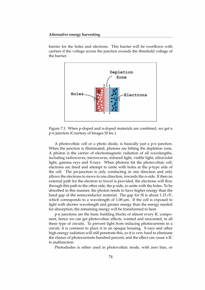
Alternative energy harvesting
barrier for the holes and electrons. This barrier will be overflown withcarriers if the voltage across the junction exceeds the threshold voltage ofthe barrier.
Figure 7.1: When p-doped and n-doped materials are combined, we get ap-n junction (Courtesy of Images SI Inc.)
A photovoltaic cell or a photo diode, is basically just a p-n junction.When the junction is illuminated, photons are hitting the depletion zone.A photon is the carrier of electromagnetic radiation of all wavelengths,including radiowaves, microwaves, infrared light, visible light, ultravioletlight, gamma rays and X-rays. When photons hit the photovoltaic cell,electrons are freed and attempt to unite with holes at the p-type side ofthe cell. The pn-junction is only conducting in one direction and onlyallows the electrons to move in one direction, towards the n-side. If then anexternal path for the electron to travel is provided, the electrons will flowthrough this path to the other side, the p-side, to unite with the holes. To beabsorbed in this manner, the photon needs to have higher energy than theband gap of the semiconductor material. The gap for SI is about 1.15 eV,which corresponds to a wavelength of 1.08 µm. If the cell is exposed tolight with shorter wavelength and greater energy than the energy neededfor absorption, the remaining energy will be transformed to heat.
p-n junctions are the basic building blocks of almost every IC compo-nent, hence we can get photovoltaic effects, wanted and unwanted, in allthese type of circuits. To prevent light from inducing photocurrents in acircuit, it is common to place it in an opaque housing. X-rays and otherhigh energy radiation will still penetrate this, so it is very hard to eliminatethe chance of photocurrents hundred percent, and the effect can cause a ICto malfunction.
Photodiodes is either used in photovoltaic mode, with zero bias, or
74
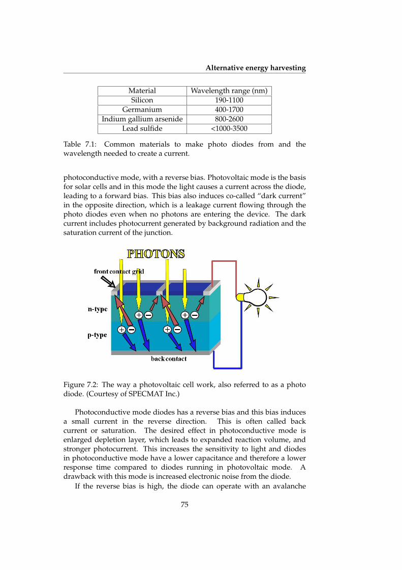
Alternative energy harvesting
Material Wavelength range (nm)Silicon 190-1100
Germanium 400-1700Indium gallium arsenide 800-2600
Lead sulfide <1000-3500
Table 7.1: Common materials to make photo diodes from and thewavelength needed to create a current.
photoconductive mode, with a reverse bias. Photovoltaic mode is the basisfor solar cells and in this mode the light causes a current across the diode,leading to a forward bias. This bias also induces co-called “dark current”in the opposite direction, which is a leakage current flowing through thephoto diodes even when no photons are entering the device. The darkcurrent includes photocurrent generated by background radiation and thesaturation current of the junction.
Figure 7.2: The way a photovoltaic cell work, also referred to as a photodiode. (Courtesy of SPECMAT Inc.)
Photoconductive mode diodes has a reverse bias and this bias inducesa small current in the reverse direction. This is often called backcurrent or saturation. The desired effect in photoconductive mode isenlarged depletion layer, which leads to expanded reaction volume, andstronger photocurrent. This increases the sensitivity to light and diodesin photoconductive mode have a lower capacitance and therefore a lowerresponse time compared to diodes running in photovoltaic mode. Adrawback with this mode is increased electronic noise from the diode.
If the reverse bias is high, the diode can operate with an avalanche
75

Alternative energy harvesting
effect, and is called avalanche photodiodes. The carriers is then multipliedby an avalanche breakdown, and the diode will get an internal gain.
7.1.2 PIN diodes
A PIN diode is a diode with an intrinsic layer between the two doped semi-conductor materials. The intrinsic layer is a wide, un-doped semiconductorregion which expands the area available for absorption of photons. A chal-lenge with the conventional diodes is the limited area of the depletion, andby using a PIN diode with a reverse bias, the bias increases the depletionregion allowing a larger volume for electron-hole pair production, reducesthe capacitance and thereby increasing the bandwidth. The PIN diode issuitable for many applications, especially the one demanding a wide dy-namic range, high bandwith or both.
When inserting an intrinsic layer, some unwanted side effects will arise.The reversed bias, that the PIN diode must have, will introduce noisecurrent which reduces the signal/noise ratio. For lower light applicationsthe PN diode is preferred, as it can be used unbiased.
Figure 7.3: Photodiode with an un-doped intrinsic semiconductor materialbetween the positive and negative doped layer.
7.1.3 Responsivity and quantum efficiency
The responsivity of a photodiode is important when calculating whethersolar energy is enough for powering the system. This measurement is theratio between the power of the incident light, which is photons, and thephotocurrent, which is a result of converted electron-hole pair. The spectralresponsivity has the units amperes per watt ( A/W), and is a function of thephotons’ wavelength since the photons have different power at differentwavelengths.
To calculate the percentage of photons hitting the photoreactive surfacethat actually will produce an electron-hole pair, we use Quantum Efficiency(QE). The QE of a sensor will then describe its response to differentwavelengths of light. This is an important measure of a photoreactivedevice, as it also gives information on the current that a cell will producewhen illuminated by a type of light. To do this, the quantum efficiency is
76

Alternative energy harvesting
integrated over a chosen electromagnetic spectrum, i.e. solar light, and thecurrent that a single cell will produce when exposed to this type of lightcan then be calculated.
In solar cell technology the External Quantum Efficiency (EQE), is themost interesting one. The EQE gives information on how much currentobtained outside the device per incoming photon.
EQE =electrons/secphotons/sec
EQE =current/(charge of 1 electron)
(total power of photons)/(energy of one photon)
The equation above shows that the external quantum efficiency bothdepends on the absorption of light and the collection of charges. When aphoton has been absorbed and it has generated an electron-hole pair, thesecharges must be separated and collected at the junction. To increase thequantum efficiency and then also the current, is important to use materialsthat prevent recombination of charges.
7.2 Kinetic energy
Another potential energy source is the energy of movement, so calledkinetic energy. When harvesting solar energy, certain conditions arerequired and the same applies for kinetic energy. Instead of availableillumination, vibrations are needed and a system powered by convertion ofkineticenergy to electric power will only be suitable for some applications.Even with a limited field of usage, it is worth looking into as RFIDtechnology can be used in various surroundings, i.e. tagging lifestock andpets with tags powered from their movements or body energy.
7.2.1 MEMS-generators
Micro Electrical Mechanical Systems (MEMS) are systems made in microscale or smaller, with mechanical parts working among with the electron-ics. These tiny mechanical systems are commercially used, i.e. in the carindustry as accelerometers in airbags, as pressure sensors in medicine andto deposit the ink in printers.
The advantage with this technology is that movable, mechanical partshave characteristics that ordinary CMOS technology do not have, and canharvest from kinetic energy. Generators made with MEMS technology arestill mostly at the research stage, but some implementations are on the mar-ket. One of the most promising available is the “electromagnetic microma-chined silicon generator” researched at the University of Southampton anddeveloped by Perpetuum Ltd. [Beeb 04].
77

Alternative energy harvesting
This generator is made on a silicon base with a coil in the middle, alongwith four magnets. The coil is located between the 4 magnets such thatthe flux lines and the direction of motion are perpendicular to the coilwindings. The coil is attached on a silicon cantilevered paddle, which isdesigned to vibrate laterally in the plane of the wafer. When the magnetsand the coil are moving relative to each other, current is induced in the coil.When reaching the resonance frequency the paddle will get the maximumamplitude, hence the largest output voltage. The generator described is lessthan 1 mm2 and output voltages of 760 mV (unloaded) is reported. With100 kΩ load, the generator can deliver close to 2 mW at 12.6 kHz [Beeb 04].These results are achieved at perfect conditions.
Figure 7.4: Electromagnetic micromachined generator. (Courtesy ofPerpetuum Ltd.)
Combined with a CMOS RFID tag, a generator like this can partlyor maybe even completely power the tag, given the right conditions.These conditions are some sort of movement when operating, causing thegenerator to oscillate, but at the same time not expose the generator to anamount of shocks causing the generator paddle to break.
7.3 Thermoelectric energy
Everywhere it is illumination, movement or heat, energy is also present.Heat can, i.e. as known from steam engines, be transformed into someother kind of energy, but when a very high temperature is not present, the
78

Alternative energy harvesting
temperature differences can also be used to produce electrical energy. Tobe dependent of temperature differences or changes to power a RFID tag,strongly limits the commercial use, but still, it is a energy source to considerwhen selecting a technology. One example is measuring devices/implantsin medicine, mounted on human skin, where a temperature differenceexists between the two surfaces of the device.
Thermoelectric devices are in the simplest form just converters whichdirectly convert temperature differences to electric voltage and vice versa.A thermoelectric device creates a voltage when there is a differenttemperature on each side, and if a voltage is applied, the device createsa temperature difference. The effect can be used to measure temperatures,to cool or heat objects or to generate electricity. Thermoelectrics are veryconvenient to use in temperature controllers, as the direction of heatingand cooling is determined by the sign of the applied voltage.
The three effects within thermoelectrics are called the Seebeck effect,the Peltier effect and the Thomson effect. The Thomson effect describesthe heating or cooling of a current-carrying conductor with a temperaturegradient and the Peltier describes the conversion of electric current to heat,so the only interesting effect in this context is the Seebeck effect, whichdescribes conversion from temperate to electric current.
7.3.1 Thermoelectrics - The Seebeck effect
In 1821 Thomas Johann Seebeck discovered the thermoelectric effect whenhe joined two wires of dissimilar metals, copper wire and bismuth wire,to form a circuit. He connected the wire ends to each other to form twojunctions, and unaware of the consequences, he heated one junction to ahigh temperature. He discovered then if the other junction remained ata cooler temperature, a magnetic field was observed around the circuit ofdifferent temperatures [Seeb 08]. The discovery was then explained onlyby the term thermomagnetism, and the generation of electrical current wasnot described until some year later.
The Seeback effect is now described as a voltage that is createdwhen a temperature difference is present between two different metals orsemiconductors. This causes a current to flow if they form a completeloop and the voltage created is of the order of several µV per degreedifference. This is called thermopower, even if it is voltage and not electricpower that is measured. Thermopower has the units of V/K and a goodthermoelectric material has thermopower of hundreds of microvolts perkelvin.
When applying a temperature difference in the setup shown infigure 7.6 on page 81, the difference will cause charged carriers, electrons orholes, in the semiconductor material, to diffuse from one side to the other.The moving charged carriers will leave behind oppositely charged nuclei
79
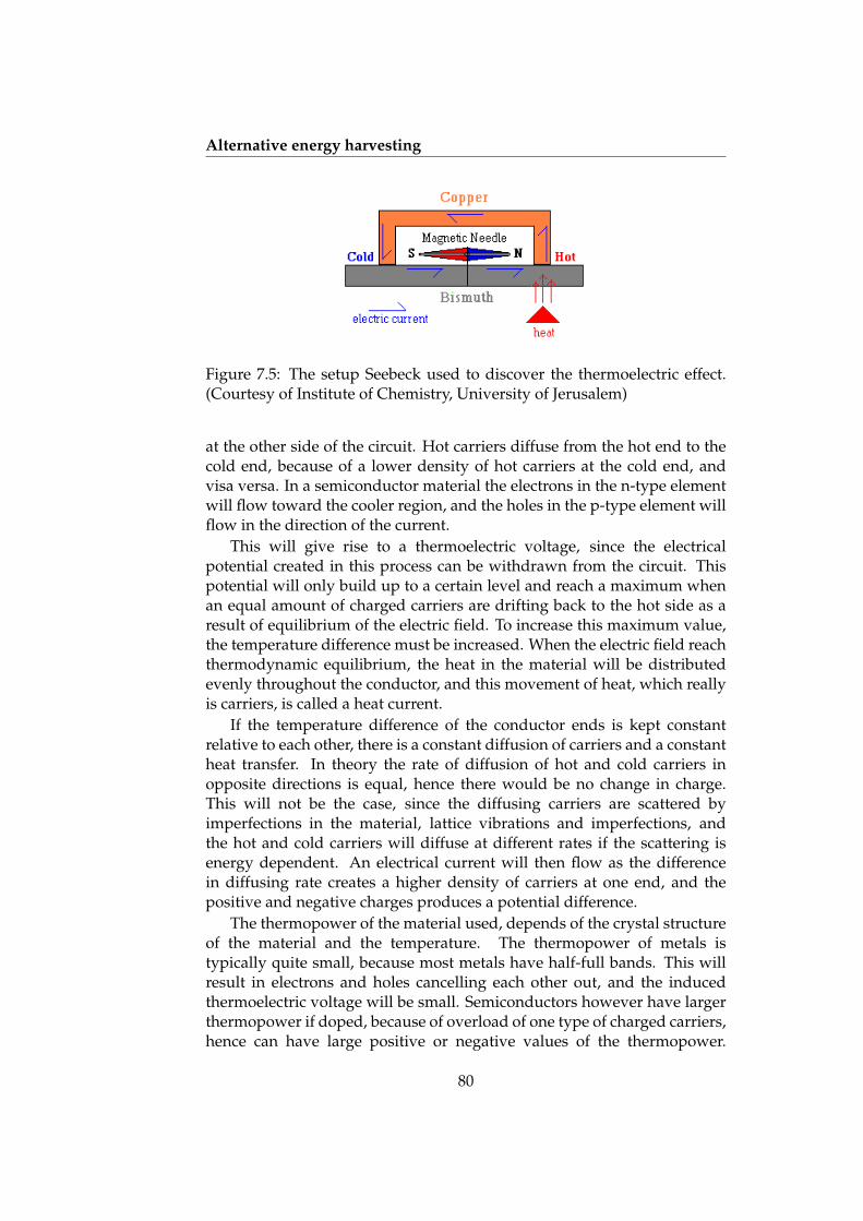
Alternative energy harvesting
Figure 7.5: The setup Seebeck used to discover the thermoelectric effect.(Courtesy of Institute of Chemistry, University of Jerusalem)
at the other side of the circuit. Hot carriers diffuse from the hot end to thecold end, because of a lower density of hot carriers at the cold end, andvisa versa. In a semiconductor material the electrons in the n-type elementwill flow toward the cooler region, and the holes in the p-type element willflow in the direction of the current.
This will give rise to a thermoelectric voltage, since the electricalpotential created in this process can be withdrawn from the circuit. Thispotential will only build up to a certain level and reach a maximum whenan equal amount of charged carriers are drifting back to the hot side as aresult of equilibrium of the electric field. To increase this maximum value,the temperature difference must be increased. When the electric field reachthermodynamic equilibrium, the heat in the material will be distributedevenly throughout the conductor, and this movement of heat, which reallyis carriers, is called a heat current.
If the temperature difference of the conductor ends is kept constantrelative to each other, there is a constant diffusion of carriers and a constantheat transfer. In theory the rate of diffusion of hot and cold carriers inopposite directions is equal, hence there would be no change in charge.This will not be the case, since the diffusing carriers are scattered byimperfections in the material, lattice vibrations and imperfections, andthe hot and cold carriers will diffuse at different rates if the scattering isenergy dependent. An electrical current will then flow as the differencein diffusing rate creates a higher density of carriers at one end, and thepositive and negative charges produces a potential difference.
The thermopower of the material used, depends of the crystal structureof the material and the temperature. The thermopower of metals istypically quite small, because most metals have half-full bands. This willresult in electrons and holes cancelling each other out, and the inducedthermoelectric voltage will be small. Semiconductors however have largerthermopower if doped, because of overload of one type of charged carriers,hence can have large positive or negative values of the thermopower.
80

Alternative energy harvesting
Similar to photoelectric effects. This positive or negative sign depends onthe charge of the dominating carriers in the material. The thermopowerof the material depends also on impurities, imperfections, structural flawsand changes. The electric field created by the circuit opposes the unevenscattering of carriers, and the equilibrium of the field is reached when netnumber of carriers in one direction are cancelling out net number of chargesin the opposite direction of the electric field.
The thermopower of a material is defined as
S =∆V∆T
=E∇T
where V is the thermoelectric voltage, T is the temperature and Ethe electric field. This is called the absolute thermopower, but is notalways of interest. This is because when measuring the voltage, thetemperature gradient will induce a thermoelectric voltage across one leg ofthe measurement electrodes. The measured thermovoltage will then havea contribution from this voltage, and can more accurately be written as
SAB = SB − SA =∆VB
∆T− ∆VA
∆T
Figure 7.6: A thermoelectric element. (Courtesy of Case Western ReserveUniversity)
The thermoelectric power and electrical conductivity maximizes some-where between a metal and semiconductors. Good thermoelectric mate-rials are typically heavily doped semiconductors or semimetals with car-rier concentration of 1019 to 1021 carriers/cm3. The materials with only one
81

Alternative energy harvesting
type of carriers, have the largest Seebeck effect, because mixed n-type andp-type conduction will lead to opposing effects and low thermopower. Bylooking at figure 7.7, we can see the thermopower of different materials andas described above, the material with the largest thermopower is a mix ofmetal and semiconductor.
Figure 7.7: The thermopower of different materials. (Courtesy of CaliforniaInstitute of Technology)
7.4 Practical use of alternative energy sources
We have now taken into consideration three different energy sources notcommonly used in wireless identification. As we can see that it is hardto power a RFID tag based sources like temperature, movements or light.Mostly because of the environmental issues like the need of a constanttemperature difference, but under the right conditions these sources can beused with success. Another problem is the space requirements. To make apractical implementable system with thermoelectric powering, quite largeelements is needed in order to maintain the temperature difference and geta high output voltage.
A photodiode or a Seebeck element, limited to a few mm2, willonly produce voltages of a few millivolts when loaded, typically a fewmicrowatts, hence they will not deliver enough current alone to power acomplete system on a tag. MEMS generators are promising devices, andat good conditions, a fair amount of power can be delivered, especiallywhen multiple devices are used. The drawback will be the constant need
82

Alternative energy harvesting
of movements, risk of shock damages and they will occupying a large area.Photo diodes is probably the most suitable technology, of these three, forwireless identification, regarding space and effect, but then the problemwith illumination will come into play.
Figure 7.8: Commercial use of thermoelectric effect, photo cells and kineticenergy.
To include solar and illumination power on a RFID tag as describedin the previous chapters, the cells have to be implemented in CMOStechnology. Since regular CMOS transistors is made from doped silicon,integration of photo cells in a standard CMOS processes is a simple task.Solar technology can also be included in the RFID tag as an externalcomponent on the side of the chip, but this will make the fabrication of thetag more expensive and complex. Silicon photodiodes are commerciallyavailable, both as PN and PIN, and by looking at datasheets from bigcommercial actors in the semiconductor industry, like Hamamatsu and OSIoptoelectronics, we can see that photodiodes and cells exists in a varietyof sizes, materials and output specifications. If the selection is narroweddown to semiconductor devices smaller than 1 mm2, the responsivity isin the range 0.2 - 0.7 A/W, and dependent of the wavelength of the lightused to illuminate the cell. The output of a photocell arrangement can befurther enlarged by the use of a chargepump, like the one in chapter 5 onpage 41. The chargepump can either be placed after the photodiodes toboost the output ([Liu 01] and [Ochi 05]), or the diodes can be integrated inthe pump itself.
Another key issue is the costs of producing the tag. When usingthermoelectric elements in small fridges, mechanical generators in wristwatches or photodiodes to power calculators this factor can be adjusted toa reasonable level. When designing a passive RFID tag, you have to keepin mind mass production and the possibility of single use. Both the sizeand costs of a single tag have to be minimized.
The conditions that have to be right for the harvesting to succeed, limitsthe use significantly, but a combination of several energy sources can be
83

Alternative energy harvesting
imaginable to use on a wireless tag. A scenario can be a illuminatedtag, with photocells charging the capacitors together with chargepumptechnology. Either as a backup system if the wireless signal gets weakend,or simultaneously to create a greater power supply for the on-chiptransmitter. But for now, these three energy sources discussed are limitedto larger applications, like the one in figure 7.8.
84

Chapter 8
Concluding remarks
The power issues in modern IC industry are one of the grand challengesof the International Technology Roadmap for Semiconductors [ITRS 07],but when the biggest concern elsewhere is to reduce temperature at smallareas, the main challenge for passive wireless technology is to get a holdof the energy. As we have seen throughout the last chapters, the energy isavailable, but it is not a trivial operation to use it. Even wireless systems,like RFID systems, are commercially ready, the potential for expanding theuse of passive tags are huge. According to the Santella Consulting, from2006 to 2007, the total spending on RFID hardware in the U.S. increasedfrom $607 to $875 billion U.S. dollars. A growth of 30%. This is much dueto larger systems, more complex readers and an massive market expansion,but still, the costs can, and should, be dramatically reduced. If the powerharvesting issues are improved, together with the transmission methods,not only reduces cost, but also improves performance.
Tags only powered by RF signals means no battery, extended lifetimeand lower cost. It is promising, but the technology has some steps to takebefore these kind of tags are able to replace semi-active tags. In manyways we can say that RFID technology is a premature technology growingup to fast, and companies world wide are using billions of dollars on atechnology, which they know little or nothing about the potential of. Theanswer to this question is not presented in this thesis, but with this work ithas been proved that energy from a RF signal is a promising source.
This thesis has presented different aspects of power harvesting, imple-mented a charge pump in CMOS technology and reviewed a selection of al-ternative energy sources. The work started with an introduction, and thennarrowed the research down to power harvesting and circuit design. Thiswas followed by a implementation of a charge pump in CMOS, simulationsand measurements. At the end of the thesis, three well known, but alterna-tive energy sources was reviewed. Alternative, because they are commonin lager applications, but not commonly used at chip level designs. The
85
Concluding remarks
results of this review have been various, but have given an understandingof what is practical doable and what is, for now, at an experimental level.
The novel diode models and couplings have been successful, and theresults from chip measurements have been satisfying, close to simulationresults. This confirms the hypothesis presented at the beginning of thisthesis, that RF signals can be used to power a passive tag. The practicalrange of this energy is yet to be known, as extensive antenna-to-chipmeasurements are not included in this thesis.
8.1 Future work
To take the circuit design of the charge pump further, there are some quiteclear fields of improvement. Some is regarding the pump itself, and otherto test the charge pump as a part of a complete system.
• An important improvement that has to be done, is to reducereflections and increase power transmission from the signal sourceor antenna to the circuit. This have to be done by adding improvedimpedance matching.
• The second aspect is more research of antennas and air transmissions.This is important in order to test the stability of the pump and abilityto generate a DC voltage from a unstable AC signal.
• To find out how the pump is working in a system, the pump shouldbe tested with a low power transmitter, and measurements shouldbe done to find required input signal at different transmission rangesand environments.
• To improve the pump further, the diodes can be replaced with pass-gates. These can be controlled by a control circuit, that will switchthe transistors on and off. This can be done to test the maximumperformance of the pump, but can also be an interesting design ifsuccessfully made.
• The charge pump has until now only be tested at certain frequencies.These were selected due to their availability, but it does not meanthat other frequencies not can be used. This will of course affect theantenna size and air loss, and also transmission regulations.
• Boost converting is another voltage boosting method worth lookingmore into. If the boosted converted DC signal is used to power aUWB-IR transmitter, the boosted signal can be “shot” into a pulse or apulse train. Since the output from the boost converter is high voltage,but low current, it is still suitable for a pulse transmitter. This might
86

Concluding remarks
not be a good idea if used together with a conventional AM or FMtransmitter, because the amount of output power would probably beto low to generate a steady carrier frequency.
• In order to test the three alternative energy sources and not justrely on measurements from articles, measurements of these areinteresting. This can be implementations in CMOS together with thecharge pump, or measurements of devices made by others. In eithercase, testing photovoltaics, MEMS generators and thermoelectrics asenergy sources together with RF signals could be of interest, and willgive a better insight to these energy forms.
87

Concluding remarks
88

Chapter 9
Acronyms
AC Alternating Current
ADC Analog to Digital Converter
ADS Active Denial System
AM Amplitude Modulation
ANA Article Number Association
ASK Amplitude Shift Keying
CMOS Complementary Metal-Oxide Semiconductor
CBI Cross-Band Interrogation
CCTV Closed Circuit Television
CEN European Committee for Standardization/Comité Européen de Nor-malisation
DC Direct Current
EAN European Article Numbering
EAS Electronic Article Surveillance
ECCC Electronic Commerce Council of Canada
EHF Extremely High Frequency (30-300 GHz)
ENG Electronic News Gathering
EPC Electronic Product Coding
EU European Union
89

Acronyms
EQE External Quantum Efficiency
FET Field Effect Transistor
FCC Federal Communications Commission
FSL Free Space Loss
FM Frequency Modulation
FSK Frequency Shift Keying
FWA Fixed Wireless Access
GSM Global System for Mobile communications
IC Integrated Circuit
IEC International Electrotechnical Commission
IEEE Institute of Electrical and Electronics Engineers
IFF Identification Friend or Foe
IR Impulse Radio
ISM Industrial, Scientific and Medical
ISO International Standards Organization
ITU International Telecommunication Union
JLCC J-Leaded Chip Carrier
LAN Local Area Network
MEMS Micro Electrical Mechanical Systems
MIT Massachusetts Institute of Technology
MOS Metal Oxide Semiconductor Field Effect Transistor
MPT Microwave Power Transmission
NASA National Space Agency
NMOS n-channel MOS
NPT Norwegian Post and Telecommunications Authority
PCB Printed Circuit Board
PMOS p-channel MOS
90
Acronyms
PSK Phase Shift Keying
QE Quantum Efficiency
RAF Royal Airforce
RCA Radio Corporation of America
RF Radio Frequency
RFID Radio Frequency Identification
SAW Surface Acoustic Wave
SHF Super High Frequency (3-30 GHz)
SMA SubMiniature version A
SPS Solar Power Satellite
SSP Space Solar Power
UCC Uniform Code Council
UHF Ultra High Frequency (0.3-3 GHz)
UWB Ultra Wide Band
WLAN Wireless Local Area Network
91

Acronyms
92
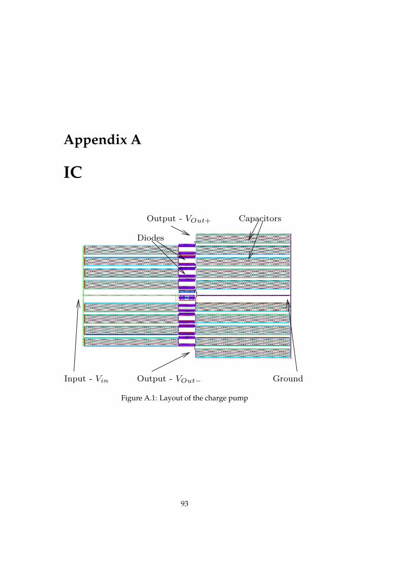
Appendix A
IC
Output - VOut− Ground
Capacitors
Diodes
Input - Vin
Output - VOut+
Figure A.1: Layout of the charge pump
93

IC
Figure A.2: Schematic of the charge pump
94

Appendix B
PCB
Figure B.1: Layout of the PCB
95

PCB
Figure B.2: Schematic of the PCB
96
Bibliography
[Alst 08] H. P. Alstad and S. Aunet. “Three Subthreshold Flip-Flop CellsCharacterized in 90 nm and 65 nm CMOS Technology”. In:Proceeding of IEEE DDECS, pp. 8–11, 2008.
[Arms 36] E. H. Armstrong. “A Method of Reducing Disturbances in RadioSignaling by a System of Frequency Modulation”. Proceedings ofthe IRE, Vol. 24, No. 5, pp. 689–740, May 1936.
[Beeb 04] S. P. Beeby, M. J. Tudor, E. Koukharenko, N. M. White,T. O’Donnell, C. Saha, S. Kulkarni, and S. Roy. “Microma-chined Silicon Generator for Harvesting Power from Vibra-tions”. The 4th International Workshop on Micro and Nanotechnol-ogy for Power Generation and Energy Conversion Applications (Pow-erMEMS 2004), 28-30th November, Kyoto, Japan 2004.
[Bene 04] M.-G. D. Benedetto and G. Giancola. Understanding UltraWide Band Radio Fundamentals. Communications Engineering andEmerging Technologies Series, Prentice Hall, June 2004.
[Brow 65] W. C. Brown. “Experimental Airborne Microwave SupportedPlatform”. Tech. Rep., Report nr. 0529474, December 1965.
[Case 82] M. T. Casey. “Nicholas Callan - priest, professor and scientist”.Physics Education, Institute of Physics Publishing, Vol. 17, No. 5,pp. 224–234, 1982.
[Chaw 07] V. Chawla and D. S. Ha. “An Overview of Passive RFID”. IEEEApplications & Practice, September 2007.
[Curt 05] J.-P. Curty, N. Joehl, C. Dehollain, and M. J. Declercq. “RemotelyPowered Addressable UHF RFID Integrated System”. IEEE J.Solid-State Circuits, Vol. 40, No. 11, pp. 2193–2202, November2005.
[Dick 76] J. F. Dickson. “On-chip high-voltage generation in NMOS inte-grated circuits using an improved voltage multiplier technique”.
97
BIBLIOGRAPHY
IEEE J. Solid-State Circuits, Vol. SC-11, No. 3, pp. 374–378, June1976.
[ERC 04] European Radiocommunications Committee (ERC). ERC Report25 - European Common Allocation Table, May 2004.
[Fano 48] R. M. Fano. “Theoretical Limitations on the Broadband Match-ing of Arbitrary Impedances”. Tech. Rep. 41, Research Labora-tory Of Electronics, Massachusetts Institute Of Technology, Jan-uary 1948.
[Fara 08] “Faraday, Michael”. Encyclopædia Britannica Online, April2008. http://www.britannica.com/eb/article-9109756.
[Fink 03] K. Finkenzeller. RFID Handbook: Fundamentals and Applications inContactless Smart Cards and Indentification. John Wiley and Sons,2 Ed., 2003.
[Grap 72] Graphical symbols for electrical power telecommunications and elec-tronics diagrams. The British Standards Institution, 1972. BS3939- Section 27.
[ITRS 07] ITRS. “International Technology Roadmap For Semiconduc-tors”. 2007.
[John 97] D. Johns and K. Martin. Analog Integrated Ciruit Design. JohnWiley & Sons, Inc, 1997.
[Kart 03] U. Karthaus and M. Fischer. “Fully Integrated passive UHFRFID transponder IC with 16.7-µW minimum RF input power”.IEEE J. Solid-State Circuits, Vol. 38, No. 10, pp. 1602–1608,October 2003.
[Land 01] D. J. Landt. “Shrouds of Time - The history of RFID”.AIM - Association for Automatic Identification and Data CaptureTechnologies, pp. 11–17, 2001.
[Lees 00] H. Leeson, P. Hansell, J. Burns, , and Z. Spasojeviç. “Demand foruse of the 2.4GHz ISM Band Final Report”. Tech. Rep., SpectrumManagement Advisory Group, Aegis Spectrum Engineering,July 2000.
[Liu 01] W.-J. Liu, O. T.-C. Chen, L.-K. Dai, P.-K. Weng, K.-H. Huang, andF.-W. Jih. “A CMOS photodiode model”. Behavioral Modelingand Simulation, 2001. BMAS 2001. Proceedings of the Fifth IEEEInternational Workshop on, pp. 102–105, 2001.
[Ludw 00] R. Ludwig and P. Bretchko. RF Circuit Design: Theory andApplications. Prentice Hall, January 2000.
98

BIBLIOGRAPHY
[Mars 03] K. M. Marsden, D. S. Ha, J. R. Armstrong, and S. Raman. A Studyof a Versatile Low Power CMOS Pulse Generator for Ultra WidebandRadios. Master’s thesis, Virginia Polytechnic Institute and StateUniversity, December 2003.
[Mill 87] J. Millman and A. Grable. Microelectronics. McGraw-Hill BookCo., second edition Ed., 1987.
[Moen 06] H. Moen. UWB Impulse Radio for RFID. Master’s thesis,Department of Informatics, University of Oslo, August 2006.
[Mors 08] “Morse, Samuel”. Encyclopædia Britannica Online, April 2008.http://www.britannica.com/eb/article-9053834/.
[Ochi 05] S. Ochi and N. Zommer. “Solar cell device having a chargepump”. US Pantent Publication, March 2005.
[Raby 70] O. Raby. Radio’s First Voice: The Story of Reginald Fessenden.MacMillan of Canada, Toronto, 1970.
[RFID 07] RFID Innovasjonssenter AS. RFID i Næringslivet, status ogtrender, GSK Konferansesenter, October 2007.
[Seeb 08] “Seebeck, Thomas”. Encyclopædia Britannica Online, April2008. http://www.britannica.com/eb/article-9066564.
[Shep 04] S. Shepard. RFID. Networking Professional, McGraw-Hill, 1 Ed.,August 2004.
[Stoc 48] H. Stockman. “Communication by Means of Reflected Power”.Proceedings of the IRE, pp. 1196–1204, October 1948.
[Stru 85] J. W. Strutt and B. Rayleigh. “On waves propagating along theplane surface of an elastic solid”. In: London Mathematical SocietyProceedings, pp. 4–11, 1885.
[Stur 08] “Sturgeon, William”. Encyclopædia Britannica Online, April2008. http://www.britannica.com/eb/article-9070045.
[Why 59] “Why Radio Amateurs Are Called "Hams"”. Florida SkipMagazine, 1959.
[Yao 05] Y. Yao, Y. Shi, and F. F. Dai. “A Novel Low-Power Input-Independent MOS AC/DC Charge Pump”. IEEE Internationalsymposium on Circuits and Systems, ISCAS, Vol. 1, pp. 380–383,23-26 May 2005.
99

BIBLIOGRAPHY
[Zhou 03] F. Zhou, D. Jin, C. Huang, and M. Hao. “Optimize thepower consumption of passive electronic tags for anti-collisionschemes”. ASIC, 2003. Proceedings. 5th International Conference on,Vol. 2, pp. 1213–1217, October 2003.
100

Paper
Power Harvesting Circuits in 90 nm Technology
Submitted for conference review.
101

Paper
102

Power Harvesting Circuits in 90 nm CMOSTrygve K. Halvorsen, Hakon A. Hjortland and Tor Sverre “Bassen” Lande
Dept. of Informatics, University of Oslo, NorwayE-mail: trygvekh, haakoh, [email protected]
Abstract— The purpose of this paper is to explore powerharvesting capabilities in nanometer technology. Novel chargepump improvements using the back-gate or well of MOS devicesimprove efficiency as well as sensitivity. The proposed circuitsare implemented in 90 nm CMOS. Measured performance willbe provided.
I. I NTRODUCTION
Power harvesting integrated as part of a standard CMOStechnology would be useful in several applications. Typicallyin RFID tags, inductive power harvesting is used [1] requiringfairly large, external inductors and working primarily in nearfield. Exploring electromagnetic waves over longer distancesis tempting and might even recover radio waves from deviceslike mobile phone or wireless LAN. To some extend thedownsizing of technology is reducing power requirements, butreduced supply voltage is limiting the controllable on-chipvoltages to less than 1 V. As circuits, both digital and analog,are exploring subthreshold transistor operation [2], powerharvesting circuit elements for fine-pitch CMOS technology isworthwhile exploring. In this paper we will present the funda-mental charge pump circuit and explore design improvementsfor better efficiency.
II. CHARGE PUMP CIRCUITS
The original Dickson charge pump [3] circuit is shown inFig. 1.
The major building blocks required are capacitors and recti-fying elements, i.e. diodes. As capacitors are readily availablein CMOS, the challenging element is the rectifier element.The first order operation of the original Dickson charge pumpis the two-phase clock that is capacitively lifting the nodecharge on the rising edges through the diode, while the diodesare preventing the charge to leak back on the negative clock
φ2
φ1
VOut
C
CS
Vin
Fig. 1. The original Dickson charge pump
COut
Step 2
Step 3
Step 4
Step 1
VOut
Fig. 2. Four-step cascode charge pump
transition. For power harvesting a single phase architecture isnecessary like the one in Fig. 2.
A single AC source is rectified and charge is built up usingcapacitors and diodes [4]. Our implementation in silicon isbased on the circuit topology of Fig. 2. By exploring the designspace of modern technology, some reasonably effective circuitsare feasible, and in the following we will explore modernCMOS technology for improved charge pump performance.
III. CMOS TECHNOLOGY OPTIONS
The optimal rectifying element would be a device with lowor no resistance when forward biased and with no conduc-tance or infinite resistance when reverse biased. The normaldiode forward biasing voltage of 0.7 V makes junction diodesunsuitable for power harvesting. Incoming antenna signals arenormally<100 mV and the forward biasing voltage must bewithin the range of the received signal. The substitute of ajunction diode in CMOS is a diode-connect MOS transistor. Inaddition, a number of different threshold voltages are availableas different devices; low, standard and high threshold. Lowgate leakage devices are also available, but sometimes thetransconductance is reduced.
As shown in Fig. 3, the differences between the thresholdvoltages are significant when comparing the 3 different devicesof 90 nm MOS transistors. In order to make the charge pumpmaximum efficient, the threshold voltages of the diodes haveto be low when pumping the voltage in order to get the voltagedrop minimized. On the other hand when pushing the chargefurther on, at the negative half-period of the input, a highthreshold is needed in order to reduce the leakage in thereverse direction of diode as much as possible. Benefits of
Paper
103

0 0.1 0.2 0.3 0.40
0.05
0.1
0.15
0.2
0.25
0.3
0.35
0.4
Voltage (V)
Cur
rent
(µA
)
High threshold modelStandard threshold modelLow threshold model
Fig. 3. MOS transistors diode-connected (low, standard and high threshold).
0 0.1 0.2 0.3 0.40
0.5
1
1.5
2
2.5
Voltage (V)
Cur
rent
(µA
)
Gate and backgate connectedConventional backgate connection
Fig. 4. A classically diode connected PMOS transistor (low threshold device)compared to one with gate and backgate connected.
increased forward current outweighs the detrimental effects ofthe increased reverse current.
Another option of modern CMOS processes is triple welldevices. With low supply voltages, the well potential may beexplored for both dynamic threshold adjustment and improvedefficiency. First we can take a look at the following equa-tion [5],
Vth = Vth0 + γ(√
Vsb + |2φF | −√|2φF |
)(1)
where γ is the body effect parameter,2φF is the surfacepotential, andVth0 is the zero bias threshold voltage.Vsbis a parameter that can be altered to achieve a lowerVth.This is done by connecting the back-gate/bulk contact to adifferent potential, hence causing a reversed body effect. Thebulk connection can be thought of as a second gate, and canalter the threshold.
With this knowledge in mind, a charge pump based on theone in Fig. 2 was designed.
IV. CMOS HIGH SENSITIVITY CHARGE PUMP
The charge pump can be described as a series of steps, andone step of the pump is shown in Fig. 5.
CC
Vn
A
Vn−1
Mna
CnVin
Mnb
Fig. 5. One step of the charge pump
This charge pump works as follows; the positive halfperiod of the input will charge capacitorCn and the diodecoupled transistor will prevent the current flowing back. Atthe throughs of the input sine wave,
VA = Vn−1 − Vth. (2)
At the peaks, this voltage rises2 ·Vin, and reaches
VA = Vn−1 − Vth + 2 ·Vin (3)
Cn will be charged toVA − Vt:Vn = Vn−1 + 2 ·Vin − 2 ·Vth (4)
Each step of the charge pump can not increase the pumpedvoltage more than two times the amplitude of the input voltageminus two times the threshold voltage of the transistors. Ifthe low-threshold models in the 90 nm technology are used,the diode threshold voltage will be 0.18 V. This means that,with no modifications to the circuit, the input amplitudemust exceed 0.18 V to get the charge pump to pump voltagethrough the steps towards the last capacitor. With the backgateconnection proposed in section III, the charge pump can workat even lower inputs.
To maximize the output voltage in this circuit, there aretwo main factors; minimize the threshold voltage or increasethe number of steps. Since increasing the number of stepswill cause degradation of power and conversion efficiency andalso increased circuit size, lowering the voltage drop of thetransistors is the most efficient way to improve the chargepump.
If we take a look at the threshold voltage of a transistor inthe triode region [5], we can see the relationship between thetransistor current and W/L.
Ids = β ·(
(VGS − Vt) ·VDS − V 2DS
2
)(5)
β = µn ·Cox · WL
(6)
To ensure pumping at low input voltages we will need alow Vth, and to ensure that we are able to deliver as muchcurrent as possible, W/L and capacitors must be as large aspossible without the capacitive load at the input of the circuitbecoming too large. This can potentially be a problem in a
Paper
104

Step 2
Step 3
Step 4
Step 1
Step 2
Step 3
Step 4
Step 1 COut+
COut−
VOut−
VOut+
Fig. 6. Charge pump with both a positive and a negative output voltage
practical implementation, because the input source will thennot be able to drive the charge pump.
Until now only a positive output voltage has been extractedfrom the charge pump, but by further developing the pumplike in Fig. 6, it can give a negative output just as big as thepositive [6]. By definingVOut− as ground, the available outputvoltage will be doubled.
V. CMOS CHARGE PUMP SIMULATIONS
The charge pump is simulated with 900 MHz and 2.45 GHzinput, and the results are shown in Fig. 7(a) and Fig. 7(b).These two frequencies are used by GSM and WLAN, and inthis range several unlicensed bands can be found [7], [8]. Theamplitude of the input signal is 100 mV. At higher frequenciesthe load will affect the circuit more and more, and will haveto be kept in mind in a practical scenario. The results arepromising for use in low-power wireless systems that requirelow voltage DC supplies.
VI. I MPLEMENTATION IN 90 NM CMOS
In Fig. 8 the layout of the chargepump is shown. It isarranged with theCC capacitors on the left and theCncapacitors on the right. The diodes are placed in the middleto avoid long wires. Two test outputs are placed in the middleof the pump for measuring purposes.
VII. C HARGE PUMP MEASUREMENTSETUP AND
PERFORMANCE
In Fig. 9 the PCB is shown. The long production time forthe process used (>6 months) has delayed our measurements.
0 5 10 15 20 25 30 35 40−0.5
−0.4
−0.3
−0.2
−0.1
0
0.1
0.2
0.3
0.4
0.5
Time (µs)
Out
put v
olta
ge (
V)
50 Ω generator and 1MΩ loadIdeal generator and no load
(a) 900 MHz
0 5 10 15 20 25 30 35 40−0.5
−0.4
−0.3
−0.2
−0.1
0
0.1
0.2
0.3
0.4
0.5
Time (µs)
Out
put v
olta
ge (
V)
50 Ω generator and 1MΩ loadIdeal generator and no load
(b) 2.45 GHz
Fig. 7. Time development of charge pump output
Output - VOut− Ground
Capacitors
Diodes
Input - Vin
Output - VOut+
Fig. 8. Layout of the charge pump
Paper
105

Fig. 9. The PCB with the chip mounted.
The results so far are good, and matches the simulations. InFig. 10(a) and 10(b) the output as a function of input signalis shown. In Fig. 10(c) the output power at different inputamplitudes and output voltages are shown. As we can seein Fig. 10(a), the symmetry in broken whenV− is belowapproximately 0.5 V. This is because the pad frame of the chiphas diodes between the pads and ground to prevent overloadingof the chip. This problem can easily be solved with use of adifferent pad frame. As Fig. 10(c) shows, the charge pump ispromising regarding power. I.e. the pump need just around300 mV input amplitude to generate 60µW with 1 V DCoutput. This can be sufficient to power a pulse transmitter,as a wireless identification tag.
VIII. C ONCLUSION
In this paper we have presented a high sensitivity chargepump suitable for power harvesting of reasonably small RFsignals commonly emitted by wireless equipment. The novelexploration of the back-gate for improved performance indi-cates the feasibility of power harvesting in devices like RFID.
REFERENCES
[1] K. Finkenzeller, RFID Handbook: Fundamentals and Applications inContactless Smart Cards and Indentification, 2nd ed. John Wiley andSons, 2003.
[2] W. M. Sansen,Analog Design Essentials, 1st ed. Springer, 2006.[3] J. F. Dickson, “On-chip high-voltage generation in nmos integrated
circuits using an improved voltage multiplier technique,”IEEE J. Solid-State Circuits, vol. 11, no. 6, pp. 374–378, June 1976.
[4] U. Karthaus and M. Fischer, “Fully integrated passive uhf rfid transponderic with 16.7-µw minimum rf input power,”IEEE J. Solid-State Circuits,vol. 38, no. 10, pp. 1602–1608, October 2003.
[5] D. Johns and K. Martin,Analog Integrated Ciruit Design. John Wiley& Sons, Inc, 1997.
[6] J.-P. Curty, N. Joehl, C. Dehollain, and M. J. Declercq, “Remotelypowered addressable uhf rfid integrated system,”IEEE J. Solid-StateCircuits, vol. 40, no. 11, pp. 2193–2202, November 2005.
[7] H. Leeson, P. Hansell, J. Burns, , and Z. Spasojevi, “Demand for useof the 2.4ghz ism band final report,” Spectrum Management AdvisoryGroup, Aegis Spectrum Engineering, Tech. Rep., July 2000.
[8] ERC Report 25 - European Common Allocation Table. EuropeanRadiocommunications Committee (ERC), May 2004.
0 50 100 150−800
−600
−400
−200
0
200
400
600
800
Amplitude of the input signal (mV)
DC
Out
put v
olta
ge (
mV
)
Unloaded2M Ω Load200k Ω Load
(a) DC output at 1 GHz
0 50 100 150−300
−200
−100
0
100
200
300
Amplitude of the input signal (mV)
DC
Out
put v
olta
ge (
mV
)
Unloaded2M Ω Load200k Ω Load
(b) DC output at 2.45 GHz
0 100 200 300 400 5000
20
40
60
80
100
Input amplitude (mV)
Out
put p
ower
(µW
)
1V output0.5V output0.2V output
(c) Output power as a function of input and outputvoltages.
Fig. 10. Results of the measurements.
Paper
106