maharashtra state board of technical education...
TRANSCRIPT

MAHARASHTRA STATE BOARD OF TECHNICAL EDUCATION (Autonomous)
(ISO/IEC - 27001 - 2005 Certified) _____________________________________________________________________________________________
1
Summer 2016 EXAMINATIONS
Subject Code: 17509 Model Answer
Important Instructions to examiners:
1) The answers should be examined by key words and not as word-to-word as given in the answer scheme.
2) The model answer and the answer written by candidate may vary but the examiner may try to assess the understanding level of the candidate.
3) The language errors such as grammatical, spelling errors should not be given more
Importance (Not applicable for subject English and Communication Skills.
4) While assessing figures, examiner may give credit for principal components indicated
in the figure. The figures drawn by candidate and model answer may vary. The examiner may give credit for any equivalent figure drawn.
5) Credits may be given step wise for numerical problems. In some cases, the assumed
constant values may vary and there may be some difference in the candidate’s answers and model answer.
6) In case of some questions credit may be given by judgment on part of examiner of
relevant answer based on candidate’s understanding.
7) For programming language papers, credit may be given to any other program based on
equivalent concept.

MAHARASHTRA STATE BOARD OF TECHNICAL EDUCATION (Autonomous)
(ISO/IEC - 27001 - 2005 Certified) _____________________________________________________________________________________________
2
Q.1 A) Attempt any THREE
a) Compare microprocessor and microcontroller (any four points)
Ans: (4M-each point)

MAHARASHTRA STATE BOARD OF TECHNICAL EDUCATION (Autonomous)
(ISO/IEC - 27001 - 2005 Certified) _____________________________________________________________________________________________
3
b) Draw and explain format of SCON register of microcontroller 8051.
Ans: (2M-format, 2M-explaination)
SM0
SCO
N.7 Serial port mode specifier
SM1 SCON.6 Serial port mode specifier.
SM2 SCON.5 Used for multiprocessor communication (Make it 0.)
REN SCON.4 Set/ cleared by software to enable/ disable reception.
TB8 SCON.3 Not widely used.
RB8 SCON.2 Not widely used
TI SCON.1 Transmit interrupt flag. Set by hardware at the beginning of the
stop Bit in mode 1.Must be cleared by software.
RI SCON.0 Receive interrupt flag. Set by hardware halfway through the
stop bit time in mode 1.Must be cleared by software.
Note: Make SM2, TB8 and RB8 = 0.
SM0 SM1
0 0 Serial Mode 0
0 1 Serial Mode 1, 8-bit data, 1 stop bit, 1 start bit
1 0 Serial Mode 2
1 1 Serial Mode 3
SM2: SM2 is the D5 bit of the SCON register. This bit enables the multiprocessing capability of the
8051. Make SM2= 0 since we are not using the 8051 in a multiprocessor environment.
REN: The REN (receive enable) bit is D4 of the SCON register. The REN bit is also referred to as
SCON.4 since SCON is a bit addressable register.
When the REN =1, it allows the 8051 to receive data on the RxD pin of the 8051. As a result if we
want the 8051 to both transfer and receive data, REN must be set to 1.
By making REN=0, the receiver is disabled. Making REN=1 or REN=0 can be achieved by the
instructions “SETB SCON.4” and “CLR SCON.4”, respectively.
This bit can be used to block any serial data reception and is an extremely important bit in the
SCON register.
TB8: TB8 (transfer bit 8) is bit D3 of SCON. It is used for serial modes 2 and 3. We make TB8=0
since it is not used in our applications.
RB8: RB8 (receive bit 8) is bit D2 of the SCON register. In serial mode 1, this bit gets copy of the
stop bit when an 8 bit data is received. This bit (as is the case for TB8) is rarely used anymore. In all
our applications we will make RB8=0. Like TB8, the RB8 bit is also used in serial modes 2 and 3.
TI: TI (transmit interrupt) is bit D1 of the SCON register.
This is an extremely important flag bit in the SCON register.
When the 8051 finishes the transfer of the 8 bit character, it raises the T1 flag to indicate that it is
ready to transfer another byte. The TI bit is raised at the beginning of the stop bit.
SM0 SM1 SM2 REN TB8 RB8 TI RI

MAHARASHTRA STATE BOARD OF TECHNICAL EDUCATION (Autonomous)
(ISO/IEC - 27001 - 2005 Certified) _____________________________________________________________________________________________
4
RI: RI(receive interrupt) is the D0 bit of the SCON register. This is another extremely important
flag in the SCON register. When the 8051 receives data serially via RxD, it gets rid of the start and
stop bits and places the byte in the SBUF register. Then it raises the RI flag bit to indicate that a
byte has been received and picked up before it is lost. RI is raised halfway through the stop bit.
c) Write ‘C’ language program to toggle all bits of Port 1 of 8051 continuously with some delay.
Ans: (4M-correct program)
#include <reg51.h>
Void MSDelay(unsigned int) ;
Void main(void)
{
While(1) //repeat forever
{
P0=0x55;
MSDelay(250) ;
P0=0xAA;
MSDelay(250);
}
}
Void MSDelay(unsigned int itime)
{
Unsigned int i, j;
For(i=0;i<itime;i++)
For(j=0;j<itime;j++) ;
}
d) State alternate pin functions of Port 3 of microcontroller 8051.
Ans: (1/2M – each pin function)
Pin Name Alternate Function
P3.0 RXD Serial input line
P3.1 TXD Serial output line
P3.2
INT0
External interrupt 0
P3.3
INT1
External interrupt 1
P3.4 T0 Timer 0 external input
P3.5 T1 Timer 1external input
P3.6
WR
External data memory write strobe
P3.7
RD
External data memory read strobe
B) Attempt any ONE

MAHARASHTRA STATE BOARD OF TECHNICAL EDUCATION (Autonomous)
(ISO/IEC - 27001 - 2005 Certified) _____________________________________________________________________________________________
5
a) Explain memory organization of 8051.
Ans: (3M-diagram,3M- explanation)
Internal memory organization
OR
Internal ROM The 8051 has 4K (4096 locations) of on-chip ROM. This is used for storing the
system program. 212 = 4096, therefore the internal ROM address bus is 12 bits wide and internal
ROM locations go from 000H to FFFH.
Internal RAM There are 256 bytes of internal RAM on the 8051. 28 = 256, therefore the internal RAM address

MAHARASHTRA STATE BOARD OF TECHNICAL EDUCATION (Autonomous)
(ISO/IEC - 27001 - 2005 Certified) _____________________________________________________________________________________________
6
bus is 8 bits wide and internal RAM locations go from 00H to FFH.
Register Banks There are four register banks from 00H to 1FH. On power-up, registers R0 to R7 are located at
00H to 07H. However, this can be changed so that the register set points to any of the other three
banks (if you change to Bank 2, for example, R0 to R7 is now located at 10H to 17H).
Bit-addressable Locations The 8051 contains 210 bit-addressable locations of which 128 are at locations 20H to 2FH while
the rest are in the SFRs. Each of the 128 bits from 20H to 2FH have a unique number (address)
attached to them, as shown in the table above. The 8051 instruction set allows you to set or reset
any single bit in this section of RAM. With the general purpose RAM from 30H to 7FH and the
register banks from 00H to 1FH, you may only read or write a full byte (8 bits) at these locations.
However, with bit-addressable RAM (20H to 2FH) you can read or write any single bit in this
region by using the unique address for that bit. We will later see that this is a very powerful
feature.
General Purpose RAM These 80 bytes of Internal RAM memory are available for general-purpose data storage. The general
purpose RAM can be accessed using direct or indirect addressing mode instructions.
Special Function Registers (SFRs) Locations 80H to FFH contain the special function registers. As you can see from the diagram
above, not all locations are used by the 8051 (eleven locations are blank). These extra locations are
used by other family members (8052, etc.) for the extra features these microcontrollers possess.
Not all SFRs are bit-addressable. Those that are have a unique address for each bit.
b) Explain following assembler directives with suitable examples
i) DB ii) ORG iii) EQU iv) END
Ans: (1.5M- each)
Ans: i) ORG:-ORG stands for Origin
Syntax:
The ORG directive is used to indicate the beginning of the address. The number that comes after ORG can be either in hex or in decimal. If the number is not followed by H, it is decimal and the assembler will convert it to hex. Some assemblers use “.ORG” (notice the dot) instead of “ORG” for the origin directive. ii) DB:- (Data Byte) Syntax:
Where byte is an 8-bit number represented in either binary, Hex, decimal or ASCII form. There should
be at least one space between label & DB. The colon (:) must present after label. This directive can be
used at the beginning of program. The label will be used in program instead of actual byte. There should
be at least one space between DB & a byte. Following are some DB examples:
ORG Address
Label: DB Byte

MAHARASHTRA STATE BOARD OF TECHNICAL EDUCATION (Autonomous)
(ISO/IEC - 27001 - 2005 Certified) _____________________________________________________________________________________________
7
iii)EQU: Equate
It is used to define constant without occupying a memory location.
Syntax:
By means of this directive, a numeric value is replaced by a symbol.
For e.g. MAXIMUM EQU 99 After this directive every appearance of the label “MAXIMUM” in the
program, the assembler will interpret as number 99 (MAXIMUM=99).
iv) END: This directive must be at the end of every program.meaning that in the source code anything after the
END directive is ignored by the assembler.
This indicates to the assembler the end of the source file(asm).
Once it encounters this directive, the assembler will stop interpreting program into machine code.
e.g. END ; End of the program.
Q.2 Attempt any TWO
a) Write an assembly language program to generate square wave of frequency 2KHz on port pin P3.0, using
timer 1of 8051.Assume oscillator frequency as 11.0592MHz.
Ans: (4M-correct program)
Crystal frequency= 11.0592 MHz I/P clock = (11.059 X 10
6)/12= 1000000 = 921.58KHz
Tin = 1.085μ sec
For 2kHz square wave
Fout = 2 KHz
Tout = 1/ 2x 10³
Tout = 500μ sec
Consider half of it = Tout = 250μ sec
N = Tout / Tin = 250/1.085 = 230.41
65536-231= (65305)10 = (FF1A)16
Program:- MOV TMOD, # 10H ; Set timer 1 in Mode 1, i.e., 16 bit timer
L2: MOV TL1, # 1AH ; Load TL register with LSB of count
MOV TH1, # FFH ; load TH register with MSB of count
SETB TR1 ; start timer 1
L1: JNB TFO, L1 ; poll till timer roll over
CLR TR1 ; stop timer 1
CPL P3.0 ; complement port 1.5 line to get high or low
CLR TF1 ; clear timer flag 1
SJMP L2 ; re-load timer with count as mode 1 is not
auto reload
b) Interface 8 bit DAC 0808 to 8051 and write ‘C’ language program to generate staircase waveform.
Ans: (4m-diagram, 4M-correct program)
Name EQU Constant

MAHARASHTRA STATE BOARD OF TECHNICAL EDUCATION (Autonomous)
(ISO/IEC - 27001 - 2005 Certified) _____________________________________________________________________________________________
8
#include<reg51.h>
Void Delat2(unsigned int );
Void main(void)
{
While(1)
{
P2=0x00;
Delay2(10);
P2=0x33;
Delay2(10);
P2=0x66;
Delay2(10);
P2=0x99;
Delay2(10);
P2=0xCC;
Delay2(10);
P2=0xFF;
Delay2(10);
}
}
Void Delay2 (unsigned int t)
{
Unsigned int x,y;
For(x=0;x<=t;x++);

MAHARASHTRA STATE BOARD OF TECHNICAL EDUCATION (Autonomous)
(ISO/IEC - 27001 - 2005 Certified) _____________________________________________________________________________________________
9
For(y=0;y<=t;y++);
}
c) Draw and explain interfacing diagram for DC motor speed control using 8051.Also develop flowchart for
the same operation.
Ans: (4M-diagram,4M-flowchart)
Q.3 Attempt any FOUR
a) Draw internal architecture diagram of 8051.
Ans: (4M-diagram)

MAHARASHTRA STATE BOARD OF TECHNICAL EDUCATION (Autonomous)
(ISO/IEC - 27001 - 2005 Certified) _____________________________________________________________________________________________
10
OR
b) State the function of Program counter (PC) and Data Pointer (DPTR) registers of 8051.
Ans: (2M-each function)
The Data Pointer (DPTR)
The Data Pointer (DPTR) is the 8051s only user-accessible 16-bit (2-byte) register. The
Accumulator, "R" registers, and "B" register are all 1-byte values.
DPTR, as the name suggests, is used to point to data. It is used by a number of commands which
allow the 8051 to access external memory. When the 8051 accesses external memory it will access
external memory at the address indicated by DPTR.

MAHARASHTRA STATE BOARD OF TECHNICAL EDUCATION (Autonomous)
(ISO/IEC - 27001 - 2005 Certified) _____________________________________________________________________________________________
11
While DPTR is most often used to point to data in external memory, many programmers often take
advantage of the fact that it is the only true 16-bit register available. It is often used to store 2-byte
values which have nothing to do with memory locations.
The Program Counter (PC) The Program Counter (PC) is a 2-byte address which tells the 8051 where the next instruction to
execute is found in memory. When the 8051 is initialized PC always starts at 0000h and is
incremented each time an instruction is executed. It is important to note that PC isnt always
incremented by one. Since some instructions require 2 or 3 bytes the PC will be incremented by 2 or
3 in these cases.
The Program Counter is special in that there is no way to directly modify its value. That is to say,
you cant do something like PC=2430h. On the other hand, if you execute LJMP 2430h you have
effectively accomplished the same thing.
c) State any four ‘C’ data types with their range of values.
Ans: (1M-each)
Data types used in C:
i)Unsigned character
range :– 0-255
2)Signed character
range :- (-128+0+127)
3)Unsigned integer
Range :- 0-65535(0000-FFFFH)
4)signed integer
range ;- (-32768 to 32767)
5) Bit
Range RAM bit addressable only
6)SFR
Range RAM addresses 80 –FFH only
7) Sbit
Range SFR bit addressable only)
d) Give four important features of 8051.
Ans: (1M-each)
Features of 8051 micro controller are as follows:- 1) 8- bit data bus and 8- bit ALU.
2) 16- bit address bus – 64KB of RAM and ROM.
3) On- chip RAM -128 (256) bytes (“ Data Memory”)
4) On- chip ROM – 4 KB (“Program Memory”)
5) Four 8-bit bi- directional input/output ports Four 8-bit bi- directional input/ output ports.
6) Programmable serial ports i.e. One UART (serial port)
7) Two 16- bit timers- Timer 0& Timer 1
8) Six interrupts are available: Reset, Two interrupts Timers i.e. Timer 0 and Timer 1, Two external
hardware interrupts- INT0 and INT1, Serial communication interrupt for both receive and transmit
e) Draw neat interfacing diagram of 20x4 LCD display with 8051 in 8 bit mode

MAHARASHTRA STATE BOARD OF TECHNICAL EDUCATION (Autonomous)
(ISO/IEC - 27001 - 2005 Certified) _____________________________________________________________________________________________
12
Q4 a)Attempt any three:
a)Draw the interfacing diagram for temperature measurement using LM 35 temperature sensor with8051
microcontroller.
b)Write ‘C” language program to send out the value 44H serially one bit at a time via P1.0 pin of
8051.TheLSB should go out first.
#include<reg51.h>
sbit=P1^o;
sbit reg_bdata=Acc^0;

MAHARASHTRA STATE BOARD OF TECHNICAL EDUCATION (Autonomous)
(ISO/IEC - 27001 - 2005 Certified) _____________________________________________________________________________________________
13
Void main(void)
{
Unsigned char a=0x44,I;
ACC=a;
For(i=1;I<=8,i++)
{
t_bit=reg_bdata;
ACC=ACC<<1;
}
}
c)Compare Von –Neumann and Harvard architecture
Any 4 difference points --4 marks .
d)List interrupts of 8051 mic with their vector address and priority upon reset and explain SFR used to
enable interrupt of 8051
Interrupt Source Vector address Interrupt priority

MAHARASHTRA STATE BOARD OF TECHNICAL EDUCATION (Autonomous)
(ISO/IEC - 27001 - 2005 Certified) _____________________________________________________________________________________________
14
External Interrupt 0 –INT0 0003H 1
Timer 0 Interrupt 000BH 2
External Interrupt 1 –INT1 0013H 3
Timer 1 Interrupt 001BH 4
Serial Interrupt 0023H 5
THE SFR used to enable interrupts is the IE SFR.
B) Attempt any 0ne:
a) Explain the operation of following instruction of 8051 with suitable example each.
i) MOVX A,@DPTR ii)SWAP A iii) SETB bit
i) MOVX A,@DPTR
Description: This instruction moves the contents of the external RAM memory pointed by (or
stored in) DPTR to accumulator.
No of bytes: 1 byte
Addressing mode: register
Example: MOV DPTR, # 2000H ; DPTR = 2000H(external RAM address)
MOV A, @DPTR ; 2000H = 0BH
;A = 0BH
ii). SWAP A
Description: This instruction exchanges bits 0-3 of the Accumulator with bits 4-7 of the
Accumulator. This instruction is identical to executing "RR A" or "RL A" four times.
No of bytes: 1 byte
Addressing mode: register specific
Example: MOV A, #59H ;A= 59H
SWAP A ; A= 95H

MAHARASHTRA STATE BOARD OF TECHNICAL EDUCATION (Autonomous)
(ISO/IEC - 27001 - 2005 Certified) _____________________________________________________________________________________________
15
iii) SETB bit Function:This sets high the bit.
.
Eg.SETB C
After execution
Set carry flag CY=1
b) Draw and explain format of TMOD and TCON registers of microcontroller 8051.
ANS:(2 marks –each format)
TMOD format:
TMOD
(89h) SFR:

MAHARASHTRA STATE BOARD OF TECHNICAL EDUCATION (Autonomous)
(ISO/IEC - 27001 - 2005 Certified) _____________________________________________________________________________________________
16
TF1 TCON. 7 Timer 1 overflowflag. Set byhardwarewhen the Timer/Counter1 overflows
Cleared byhardware as processor vectors to theinterrupt service routine.
TR1 TCON. 6 Timer 1 run control bit. Set/cleared bysoftware to turn
Timer/Counter1ON/OFF. TF0 TCON. 5 Timer 0 overflow flag. Set byhardwarewhen the Timer/Counter0
overflows.
Cleared by hardware as processor vectors to the service routine.
TR0 TCON. 4 Timer 0 run control bit. Set/cleared by software to turn Timer/Counter 0
ON/OFF.
IE1 TCON. 3 ExternalInterrupt 1 edge flag. Set byhardware when External
Interruptedgeis detected. Cleared by hardware when interrupt is processed.
IT1 TCON. 2 Interrupt 1 typecontrol bit. Set/cleared by softwareto specifyfalling
edge/lowlevel triggered External Interrupt.
IE0 TCON. 1 ExternalInterrupt 0 edge flag. Set byhardware when External
Interruptedgedetected. Cleared byhardwarewhen interrupt is processed.
IT0 TCON. 0 Interrupt 0 typecontrol bit. Set/cleared by softwareto
Specify falling edge/low level triggered External Interrupt.
Q5) Attempt any two:
a)Draw interfacing diagram of 3x3 matrix keyboard with 8051 and write ‘C” language program to read key
status

MAHARASHTRA STATE BOARD OF TECHNICAL EDUCATION (Autonomous)
(ISO/IEC - 27001 - 2005 Certified) _____________________________________________________________________________________________
17
# include < reg51.h>
# define COL P2 // define ports for easier reading
# define ROW P1
void MSDelay ( unsigned int value) ;
void SerTX ( unsigned int value ) ;
unsigned char keypad [3] [3] = { ‘0’ , ‘1’ ,’2’ ,’3’ , ’4’, ‘5’ ,’6’ ,’7’ ,’8’};
void main()
{
Unsigned char colloc, rowloc ;
TMOD = 0X20; // timer 1, mode 2
THI= -3; // 9600 baud
SCON = 0X50;// 8 – bit , 1 stop bit
TR1 = 1;// start timer 1
// keyboard routine . This sends the ASCII
// code for pressed key to the serial port
COL = 0XFF; // make P2 an input port
While (1) // repeat for ever

MAHARASHTRA STATE BOARD OF TECHNICAL EDUCATION (Autonomous)
(ISO/IEC - 27001 - 2005 Certified) _____________________________________________________________________________________________
18
{
do
{
ROW = 0X00; // ground all rows at once
Colloc = COL; // read the columns
Colloc &=0X0F; // mask used bits
} while ( colloc ! = 0X0F); // check until all keys released
do
{
Do
{
MSDelay(20); // call delay
colloc = COL ; // see if any key is pressed
colloc &= 0X0F; //mask unused bits
} while (colloc = = 0X0F ); // wait for keypress
While(1)
{
ROW = 0XFE; // ground row 0
colloc = COL; // read columns
colloc &= 0X0F; // mask unused bits
if ( colloc ! = 0X0F // column detected
{
rowlock = 0; // save row location
break ; // exit while loop
}
ROW = 0XFD; // ground row 1
colloc = COL; // read columns

MAHARASHTRA STATE BOARD OF TECHNICAL EDUCATION (Autonomous)
(ISO/IEC - 27001 - 2005 Certified) _____________________________________________________________________________________________
19
colloc &= 0X0F; // mask unused bits
if ( colloc ! = 0X0F // column detected
{
rowlock = 1; // save row location
break ; // exit while loop
ROW = 0XFB; // ground row 2
colloc = COL; // read columns
colloc &= 0X0F; // mask unused bits
if ( colloc ! = 0X0F // column detected
{
rowlock = 2; // save row location
break ; // exit while loop
}
// check column and send result to the serial port
If ( colloc = = 0X0E)
SerTX ( keypad[rowlock] [0]);
else if ( colloc = = 0X0D)
SerTX ( keypad[rowlock] [1]);
else if ( colloc = = 0X0B)
SerTX ( keypad[rowlock] [2]);
}
Void SerTX ( unsigned char x)
{
SBUF = x; // place value in buffer
While ( T1 = = 0) ; // wait until transmitted
TI = 0; // clear flag
}
Void MSDelay ( unsigned int value )

MAHARASHTRA STATE BOARD OF TECHNICAL EDUCATION (Autonomous)
(ISO/IEC - 27001 - 2005 Certified) _____________________________________________________________________________________________
20
{
unsigned int x, y;
for ( x= 0; x<1275;x++ )
for ( y = 0; y< value ; y++ ) ;
}
b)Write algorithm and assembly language program to add two BCD numbers stored at internal RAM
locations 40 H and 41H .store the result at internal RAM location 42H.
ALgorithm
Load the contents of mem location 40H into accumulator
Add contents of accumulator with contents of mem location
Adjust result to BCD
Store the result in mem location 42H
Program
MOV A,40H ;Load the contents of mem location 40H into accumulator
ADD A,41H ;Add contents of accumulator with contents of mem location
DAA ;Adjust result to BCD
MOV 42H,A ;Store the result in mem location 42H
Sjmp $

MAHARASHTRA STATE BOARD OF TECHNICAL EDUCATION (Autonomous)
(ISO/IEC - 27001 - 2005 Certified) _____________________________________________________________________________________________
21
c)Draw the diagram to interface 8 switches to Port 1 and 8 LED’s to Port 2 of 8051.Write “C” language program to display switch status on LED’s
MAHARASHTRA STATE BOARD OF TECHNICAL EDUCATION (Autonomous)
(ISO/IEC - 27001 - 2005 Certified) _____________________________________________________________________________________________
22
Q6)Attempt any four:
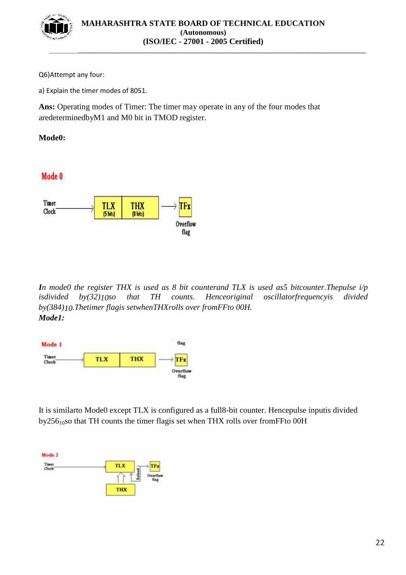
a) Explain the timer modes of 8051.
Ans: Operating modes of Timer: The timer may operate in any of the four modes that
aredeterminedbyM1 and M0 bit in TMOD register.
Mode0:
In mode0 the register THX is used as 8 bit counterand TLX is used as5 bitcounter.Thepulse i/p
isdivided by(32)10so that TH counts. Henceoriginal oscillatorfrequencyis divided
by(384)10.Thetimer flagis setwhenTHXrolls over fromFFto 00H.
Mode1:
It is similarto Mode0 except TLX is configured as a full8-bit counter. Hencepulse inputis divided
by25610so that TH counts the timer flagis set when THX rolls over fromFFto 00H

MAHARASHTRA STATE BOARD OF TECHNICAL EDUCATION (Autonomous)
(ISO/IEC - 27001 - 2005 Certified) _____________________________________________________________________________________________
23
In this modeonlyTLX isused as 8-bitcounter. THXis used to hold the value which is
loadedin TLX initially.EverytimeTLX overflows from FFH to 00H thetimer flagis set
and thevalue from THX is automaticallyreloaded in TLXregister.
Mode 3
In this mode, timer0 becomes two completed separate 8-bittimers. TL0 is controlled
bygatearrangement oftimer0and sets timer 0 flag when itoverflows.TH0 receives the timerclock
under the control of TR1 bit and sets TF1 flagwhen itoverflows. Timer 1 maybeused in mode 0, 1
and 2 with oneimportant exception that no interrupt will be generated bythe timer when the timer 0
is usingTF1 overflow flag
Draw circuit diagram to interface common anode 7 segment display to 8051 and write „C‟ language
program to display number 0.
OR
8
0
5
1

MAHARASHTRA STATE BOARD OF TECHNICAL EDUCATION (Autonomous)
(ISO/IEC - 27001 - 2005 Certified) _____________________________________________________________________________________________
24
Program:
// C language program for 7 Segment display interfacing
#include <Intel\8052.h>
#include <standard.h>
/*SEVEN SEGMENT DISPLAY
DP G F E D C B A
NO D7 D6 D5 D4 D3 D2 D1 D0
0 0 1 0 0 0 0 0 0 =40H
A = P1.0 B = P1.1 C = P1.2 D = P1.3
E = P1.4 F = P1.5 G = P1.6 DP= P1.7
*/
void main ()
{
P1 = 0xFF; //DISPLAY OFF
while(1)
{
P1 = 0x40; //DISPLAY 0

MAHARASHTRA STATE BOARD OF TECHNICAL EDUCATION (Autonomous)
(ISO/IEC - 27001 - 2005 Certified) _____________________________________________________________________________________________
25
delay_ms(1000);
}
}
NOTE: Program may change. Student can also use the other logic.
Please check the logic and understanding of students.
c)List any four addressing modes of 8051 with one example each.
Ans: (1 Mark—each addressing mode with example --any four)
There are a number of addressing modes available to the 8051 instruction set, as follows:
1. Immediate Addressing mode
2. Register Addressing mode
3. Direct Addressing mode
4 Register Indirect addressing mode
5. Relative Addressing mode
6. Absolute addressing mode
7. Long Addressing mode
8. Indexed Addressing mode
1) Immediate Addressing mode:
Immediate addressing simply means that the operand (which immediately follows the Instruction
op. code) is the data value to be used.
For example the instruction:
MOV A, #25H; Load 25H into A
Moves the value 25H into the accumulator The # symbol tells the assembler that the immediate
addressing mode is to be used.
2 )Register Addressing Mode:
One of the eight general-registers, R0 to R7, can be specified as the instruction Operand. The
assembly language documentation refers to a register generically as Rn.
An example instruction using register addressing is :
ADD A, R5 ; Add the contents of register R5 to contents of A (accumulator)
Here the contents of R5 are added to the accumulator. One advantage of register addressing is that
the instructions tend to be short, single byte instructions.
3) Direct Addressing Mode:
Direct addressing means that the data value is obtained directly from the memory location specified
in the operand.
For example consider the instruction:
MOV R0, 40H; Save contents of RAM location 40H in R0.
The instruction reads the data from Internal RAM address 40H and stores this in theR0. Direct
addressing can be used to access Internal RAM, including the SFR registers.
4) Register Indirect Addressing Mode:
Indirect addressing provides a powerful addressing capability, which needs to be appreciated.
An example instruction, which uses indirect addressing, is as follows:
MOV A, @R0; move contents of RAM location whose address is held by R0 into A
Note the @ symbol indicated that the indirect addressing mode is used. If the data is inside the
CPU, only registers R0 & R1 are used for this purpose.
5) Relative Addressing Mode:

MAHARASHTRA STATE BOARD OF TECHNICAL EDUCATION (Autonomous)
(ISO/IEC - 27001 - 2005 Certified) _____________________________________________________________________________________________
26
CY AC F0 RS1 RS0 OV -- P
This is a special addressing mode used with certain jump instructions. The relative address, often
referred to as an offset, is an 8-bit signed number, which is automatically added to the PC to make
the address of the next instruction. The 8-bitsigned offset value gives an address range of + 127 to –
128 locations.
Consider the following example:
SJMP LABEL_X
An advantage of relative addressing is that the program code is easy to relocate in memory in that
the addressing is relative to the position in memory.
6) Absolute addressing Mode:
Absolute addressing within the 8051 is used only by the AJMP (Absolute Jump) and ACALL
(Absolute Call) instructions.
7) Long Addressing Mode:
The long addressing mode within the 8051 is used with the instructions LJMP and LCALL. The
address specifies a full 16 bit destination address so that a jump or a call can be made to a location
within a 64KByte code memory space (216 = 64K).
An example instruction is:
LJMP 5000h; full 16 bit address is specified in operand.
8) Indexed Addressing Mode:
With indexed addressing a separate register, either the program counter, PC, or the data pointer
DTPR, is used as a base address and the accumulator is used as an offset address. The effective
address is formed by adding the value from the base address to the value from the offset address.
Indexed addressing in the 8051 is used with the JMP or MOVC instructions. Look up tables are
easy to implement with the help of index addressing.
Consider the example instruction:
MOVC A, @A+DPTR
MOVC is a move instruction, which moves data from the external code memory space. The address
operand in this example is formed by adding the content of the DPTR register to the accumulator
value. Here the DPTR value is referred to as the base address and the accumulator value us referred
to as the index address.
d) Draw the format of PSW register of 8051 with one example each.
CY
PSW.7 CarryFlag.
AC PSW.6 Auxiliarycarryflag.
F0 PSW.5 Available to the userforgeneral purpose.
RS1 PSW.4 Register bank selector bit 1.
RS0 PSW.3 Register bank selector bit 0.
OV PSW.2 Overflowflag.

MAHARASHTRA STATE BOARD OF TECHNICAL EDUCATION (Autonomous)
(ISO/IEC - 27001 - 2005 Certified) _____________________________________________________________________________________________
27
-- PSW.1 User-definable bit.
P PSW.0 Parity flag. Set/cleared by hardware each instruction cycle to
indicateand Odd/even numberof 1 bit in the accumulator. 1. CY:the carry flag.This flag is set whenever there is a carryout from the D7 bit. The flag bitis
affected after an 8 bit addition or subtraction.
It can also be set to 1 or0 directly by an instruction such as“SETBC” and
CLR C”where“SETBC”stands for “set bit carry”and“CLR C” for “clear carry”.
2. AC:the auxiliary carry flag If there is a carry from D3 and D4 during an ADD or SUB operation,
this bit is set; it is cleared. This flag is used by instructions that perform BCD (binarycoded
decimal)arithmetic.
3. F0:Available to theuser forgeneral purposes.
4. RS0, RS1: register bank selects bits These two bits are used to select one of the four register
banks n internal RAM in the table. By writing zeroes and ones to these bits, a group of registers R0-
R7can be used out off our registers banks in internal RAM.
RS1 RS0 Spacein RAM 0 0 Bank 0 (00H-07H) 0 1 Bank 1 (08H-0FH) 1 0 Bank2 (10H-17H) 1 1 Bank3 (18H-1FH)
.OV:
Overflow
flag
This flag is set whenever the result of a signed number operation is too large, causing thehigh-
order bit to overflow into the sign bit. In general, the carry flag is used to detect errors in
unsigned arithmetic operations. The over flow flag is only used to detect errors in signed
arithmetic operations.
6.P:Parity
flag
The parity flag reflects the number of 1sin the A(accumulator) register only.If the A register
contains an odd number of 1s, then P=1.P=0 if A has an even number of 1s.

MAHARASHTRA STATE BOARD OF TECHNICAL EDUCATION (Autonomous)
(ISO/IEC - 27001 - 2005 Certified) _____________________________________________________________________________________________
28
e)Draw interfacing diagram to interface relay to port pin P3.0 and opto isolator to port pin P3.7 of 8051
microcontroller