model answers summer 2019 examinations subject & code: electrical circuits & networks...
TRANSCRIPT

MAHARASHTRA STATE BOARD OF TECHNICAL EDUCATION
(Autonomous)
(ISO/IEC-27001-2013 Certified)
Model Answers
Summer – 2019 Examinations
Subject & Code: Electrical Circuits & Networks (17323)
Page No: 1 of 24
Important Instructions to examiners:
1) The answers should be examined by key words and not as word-to-word as given in the model
answer scheme.
2) The model answer and the answer written by candidate may vary but the examiner may try to assess
the understanding level of the candidate.
3) The language errors such as grammatical, spelling errors should not be given more importance (Not
applicable for subject English and Communication Skills).
4) While assessing figures, examiner may give credit for principal components indicated in the figure.
The figures drawn by candidate and model answer may vary. The examiner may give credit for any
equivalent figure drawn.
5) Credits may be given step wise for numerical problems. In some cases, the assumed constant values
may vary and there may be some difference in the candidate’s answers and model answer.
6) In case of some questions credit may be given by judgement on part of examiner of relevant answer
based on candidate’s understanding.
7) For programming language papers, credit may be given to any other program based on equivalent
concept.

MAHARASHTRA STATE BOARD OF TECHNICAL EDUCATION
(Autonomous)
(ISO/IEC-27001-2013 Certified)
Model Answers
Summer – 2019 Examinations
Subject & Code: Electrical Circuits & Networks (17323)
Page No: 2 of 24
1 Attempt any TEN of the following: 20
1 a) Define waveform and instantaneous value of an alternating quantity.
Ans:
i) Waveform: It is a graph of magnitude of an AC quantity against time.
ii) Instantaneous value: It is defined as the value of an AC quantity at a particular
instant of time.
1 mark
1 mark
1 b) An alternating voltage is having maximum value 230 volt. What is its average value
and rms value?
Ans:
Assuming that the alternating quantity is a sinusoidal quantity,
i) Average value = 0.637 × maximum value = 0.637 × 230
Average value = 146.51 volt
ii) RMS value = 0.707 × maximum value = 0.707×230
RMS value = 162.61 volt.
1 mark
1 mark
1 c) Define Inductive reactance and Capacitive reactance.
Ans:
i) Inductive reactance:
The opposition offered by the inductance of a circuit to the flow of an alternating
current is called an inductive reactance.
It is denoted by “XL” and given by XL = 2πfL Ω
ii) Capacitive reactance:
The opposition offered by the capacitance of a circuit to the flow of an alternating
current is called an capacitive reactance.
It is denoted by “XC” and given by XC = 𝟏
𝟐𝛑𝐟𝐂Ω
1 mark
1 mark
1 d) Define power factor and reactive power.
Ans -
i) Power factor:
It is the cosine of the angle between the applied voltage and the resulting
current.
Power factor = cosΦ
where, Φ is the phase angle between applied voltage and current.
OR
It is the ratio of true or effective or real power to the apparent power.
Power factor = True Or Effective Or Real Power /Apparent Power
= VI cosΦ / VI
= cosΦ
OR
It is the ratio of circuit resistance to the circuit impedance.
Power factor =Circuit Resistance / Circuit Impedance
= R / Z
= cosΦ
ii) Reactive Power:
1 mark

MAHARASHTRA STATE BOARD OF TECHNICAL EDUCATION
(Autonomous)
(ISO/IEC-27001-2013 Certified)
Model Answers
Summer – 2019 Examinations
Subject & Code: Electrical Circuits & Networks (17323)
Page No: 3 of 24
Reactive power (Q) is the product of voltage, current and the sine of the phase
angle between voltage and current.
Q =VIsinΦ volt-amp-reactive
OR
It is the quantity of “unused” power that is developed by reactive components
in an AC circuit.
1 mark
1 e) Draw a admittance triangle by considering capacitive susceptance and inductive
susceptance.
Ans:
1 mark each
= 2 marks
1 f) Give any two applications of parallel resonant circuits.
Ans:
Applications of parallel resonant circuits:
i) An oscillator circuit
ii) As current amplifier
iii) As current rejector
iv) Load impedance in output circuits of RF amplifiers.
v) It can be used in induction heating.
vi) In filter circuits.
vii) Tank circuit.
viii) Power-factor improvement circuit
1 mark for
each of any
two
applications
= 2 marks
1 g) State the relations between line and phase values of voltage and current for balanced
star connected load.
Ans:
For balanced star connected load,
Line voltage =√3 x Phase Voltage
i.e VL = √3 x Vph
Line current = Phase current
i.e IL = Iph
1 mark
1 mark
1 h) Define phase sequence of three phase ac quantity.
Ans:
Phase Sequence:
Phase sequence is defined as the order in which the voltages (or any other alternating
quantity) of the three phases attain their positive maximum values.
In the waveforms, it is seen that the R-phase voltage attains the positive maximum
value first, and after angular distance of 120, Y-phase voltage attains its positive
1 mark for
correct
definition
MAHARASHTRA STATE BOARD OF TECHNICAL EDUCATION
(Autonomous)
(ISO/IEC-27001-2013 Certified)
Model Answers
Summer – 2019 Examinations
Subject & Code: Electrical Circuits & Networks (17323)
Page No: 4 of 24
maximum and further after 120, B-phase voltage attains its positive maximum value.
So the phase sequence is R-Y-B.
1 mark for
diagram
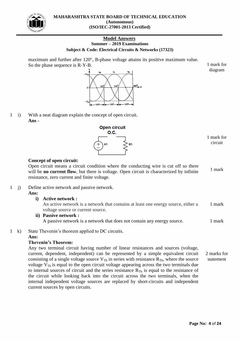
1 i) With a neat diagram explain the concept of open circuit.
Ans -
Concept of open circuit:
Open circuit means a circuit condition where the conducting wire is cut off so there
will be no current flow, but there is voltage. Open circuit is characterized by infinite
resistance, zero current and finite voltage.
1 mark for
circuit
1 mark
1 j) Define active network and passive network.
Ans:
i) Active network :
An active network is a network that contains at least one energy source, either a
voltage source or current source.
ii) Passive network :
A passive network is a network that does not contain any energy source.
1 mark
1 mark
1 k) State Thevenin’s theorem applied to DC circuits.
Ans:
Thevenin’s Theorem:
Any two terminal circuit having number of linear resistances and sources (voltage,
current, dependent, independent) can be represented by a simple equivalent circuit
consisting of a single voltage source VTh in series with resistance RTh, where the source
voltage VTh is equal to the open circuit voltage appearing across the two terminals due
to internal sources of circuit and the series resistance RTh is equal to the resistance of
the circuit while looking back into the circuit across the two terminals, when the
internal independent voltage sources are replaced by short-circuits and independent
current sources by open circuits.
2 marks for
statement

MAHARASHTRA STATE BOARD OF TECHNICAL EDUCATION
(Autonomous)
(ISO/IEC-27001-2013 Certified)
Model Answers
Summer – 2019 Examinations
Subject & Code: Electrical Circuits & Networks (17323)
Page No: 5 of 24
1 l) Give the meaning of “Steady state condition” and state the behavior of pure C at steady
state condition.
Ans:
Meaning of Steady state condition:
Steady state condition is that condition which exists after all initial transients or
fluctuations have damped out and all currents, voltages or fields are settles down to
essentially constant values.
Usually the steady state is said to be reached at time instant t → .
Steady state behavior of Pure C:
At steady state condition the capacitor acts as open circuit.
1 mark
1 mark
2 Attempt any FOUR of the following: 16
2 a) Instantaneous expression for voltage and current are given by
V = 141.4sin314t, i = 28.28sin (314t + π/3)
Determine:
i) Voltmeter and ammeter reading.
ii) Frequency of current
iii) Power factor
iv) Power consumed.
Ans:
Data Given:
V = 141.4sin314t, i = 28.28sin (314t + π/3)
i) Voltmeter and Ammeter reading:
Voltmeter reads RMS value:
Vrms = 0.707 x Vm = 0.707 x 141.4 = 99.97 V ≈ 100 V
Voltmeter reading = 99.97 V i.e. 100V
Ammeter reads RMS value:
Irms = 0.707 x Im = 0.707 x 28.28 = 19.99 A i.e. 20A
Ammeter reading = 19.99A ≈ 20A.
ii) Frequency of current
Comparing the current equation with standard equation
I = Im sin(ωt+Φ) amp
we get, ω = 314
we know that, f = ω /2π = 314/2π
Frequency of current f = 49.97 Hz ≈ 50 Hz
iii) Power factor:
Power Factor = Cos(Φ) = Cos (π/3)
Power factor = 0.5 leading
iv) Power consumed:
P = V x I x CosΦ = 99.97 x 19.99 x 0.5
Power consumed = 999.2 Watt ≈ 1000 Watt
½ mark
½ mark
1 mark
1 mark
1 mark

MAHARASHTRA STATE BOARD OF TECHNICAL EDUCATION
(Autonomous)
(ISO/IEC-27001-2013 Certified)
Model Answers
Summer – 2019 Examinations
Subject & Code: Electrical Circuits & Networks (17323)
Page No: 6 of 24
2 b) Derive the expression for current and voltage in pure resistive circuit when connected
to sinusoidal AC voltage. Draw the phasor diagram.
Ans:-
Referring to fig. the instantaneous voltage across the resistor (vR) is same as source
voltage.
Therefore, vR = v = Vm sin(ωt) ………………………….(1)
Applying ohms law, the expression for the instantaneous current flowing through the
resistor is given by, i = vR / R
i = Vm sin(ωt) / R = (Vm/R) sin(ωt)
where, Im = Vm/R , i = Im0o
Therefore, I = Imsin(ωt) …………………………………(2)
On comparing Eq. (1) and (2), we conclude that,
The current flowing through a purely resistive ac circuit is sinusoidal.
The current through the resistive circuit and the applied voltage are in phase
with each other.
1 mark for
circuit
diagram
1 mark for
phasor
diagram
2 marks for
derivation
2 c) For the given impedance triangle as shown in Fig. No. 1.
i) Identify the type of circuit.
ii) Mark parameters of all sides of the triangle
iii) State the nature of power factor
iv) Draw a sinusoidal waveform of voltage and current.
Ans:
i) The types of circuit:
Type of circuit is R-L series circuit.
ii) Parameters of all sides of the triangle:
1 mark for
each bit
= 4 marks

MAHARASHTRA STATE BOARD OF TECHNICAL EDUCATION
(Autonomous)
(ISO/IEC-27001-2013 Certified)
Model Answers
Summer – 2019 Examinations
Subject & Code: Electrical Circuits & Networks (17323)
Page No: 7 of 24
iii) Nature of power factor:
The nature of power factor is lagging.
iv) Sinusoidal waveform of voltage and current:
2 d) Define the impedance and draw the impedance triangle.
Ans:
i) Definition of Impedance: The impedance (Z) of the circuit is defined as the total
opposition of the circuit to the alternating current flowing through it.
OR It is combined effect produced by the resistance, inductive reactance and
capacitive reactance in the AC circuit.
It is denoted by “Z” and measured in ohm.
ii) Impedance Triangle:
For R-L series circuit For R-C series circuit
2 marks for
definition
1 mark for
each triangle
= 2 marks
2 e) A resistance of 100Ω and 50µf capacitor are connected in series across a 230V, 50Hz
supply. Find:
i) The impedance.
ii) The current flowing through the circuit.
iii) Voltage across resistance and capacitance.
iv) Power factor and Power.
Ans:
V= 230∠0 volts, f = 50Hz R = 100 C = 50F = 50×10-6
F

MAHARASHTRA STATE BOARD OF TECHNICAL EDUCATION
(Autonomous)
(ISO/IEC-27001-2013 Certified)
Model Answers
Summer – 2019 Examinations
Subject & Code: Electrical Circuits & Networks (17323)
Page No: 8 of 24
Capacitive Reactance (XC):
XC = 1 / (2πfC)
= 1 / (2π x 50 x 50 x 10-6
)
XC = 63.66 Ω
i) Impedance (Z) = √(R2 + XC
2)
= √(1002 + 63.66
2)
Z = 118.54 Ω
ii) The current flowing through the circuit (I) :
I = V / Z
= 230 / 118.54
I = 1.94 amp
iii) Voltage across resistance(VR) and capacitance(VC)
Voltage across resistance(VR) = I x R = 1.94 x 100
= 194 Volt
Voltage across capacitance(VC) = I x Xc = 1.94 x 63.66
= 123.5 Volt
iv) Power factor and Power.
Power Factor (CosΦ) = R / Z = 100 / 118.54
= 0.84 (leading)
Power (P) = V x I x COSΦ = 230 x 1.94 x 0.84
= 374.80 Watt
1 mark for
each bit
= 4 marks
2 f) A circuit consists of a resistance of 20Ω in series with an inductance of 95.6 mH and a
capacitor of 318µf. It is connected to a 500V, 25Hz supply. Find the current in the
circuit and power factor.
Ans:
Data Given: R = 20Ω, L = 95.6 mH = 95.6 x 10⁻³
H C = 318 µf = 318 x 10-6
F
V = 500V f = 25Hz.
Inductive Reactance :
XL = 2πfL = 2π x 25 x 95.6 x 10-3
XL = 15.01 Ω
Capacitive Reactance :
XC = 1/2πfc = 1/(2π x 25 x 318 x 10-6
)
XC = 20.01 Ω
Impedance :
Z = √R2 + (XL - XC)
2 = √20
2 + (15.01 – 20.01)
2
Z = 20.61 Ω
i) Current in the circuit(I): I = V / Z = 500 / 20.61
I = 24.26 amp
ii) Power factor (cosΦ):
cosΦ = R / Z = 20 / 20.61
cosΦ = 0.97 (leading)
½ mark
½ mark
1 mark for Z
1 mark for I
1 mark for pf
3 Attempt any FOUR of the following: 16
MAHARASHTRA STATE BOARD OF TECHNICAL EDUCATION
(Autonomous)
(ISO/IEC-27001-2013 Certified)
Model Answers
Summer – 2019 Examinations
Subject & Code: Electrical Circuits & Networks (17323)
Page No: 9 of 24
3 a) Compare series resonance circuit with parallel resonance circuit.
Ans:
Comparison between series and parallel resonance circuit:
Sr. No. Series resonant Circuit Parallel resonant Circuit
1
𝑓𝑟 =1
2𝜋√𝐿𝐶
For series R-L-C circuit, the
resonance frequency is,
𝑓𝑟 =1
2𝜋√𝐿𝐶
For parallel R-L-C circuit, the
resonance frequency is,
2
At resonance, the series RLC
circuit offers minimum total
impedance Z = R
At resonance, the parallel RLC
circuit offers maximum total
impedance Z =L/CR
3
At resonance, series RLC
circuit draws maximum
current from source, I =
(V/R)
At resonance, parallel RLC
circuit draws minimum current
from source, 𝐼 =𝑉
[𝐿𝐶𝑅⁄ ]
4
At resonance, in series RLC
circuit, voltage magnification
takes place.
At resonance, in parallel RLC
circuit, current magnification
takes place.
5
𝑄 =1
𝑅√
𝐿
𝐶
The Q-factor for series
resonant circuit is
The Q-factor for parallel
resonant circuit is,
𝑄 =1
𝑅√
𝐿
𝐶
6 Series RLC resonant circuit
is Accepter circuit.
Parallel RLC resonant circuit is
Rejecter circuit.
1 mark for
each of any
four points
= 4 marks
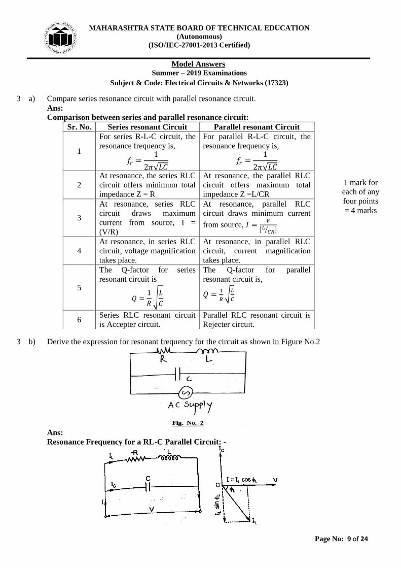
3 b) Derive the expression for resonant frequency for the circuit as shown in Figure No.2
Ans:
Resonance Frequency for a RL-C Parallel Circuit: -

MAHARASHTRA STATE BOARD OF TECHNICAL EDUCATION
(Autonomous)
(ISO/IEC-27001-2013 Certified)
Model Answers
Summer – 2019 Examinations
Subject & Code: Electrical Circuits & Networks (17323)
Page No: 10 of 24
The circuit is said to be in electrical resonance when the reactive component of line
current becomes zero. The frequency at which this happens is known as resonance
frequency.
Net reactive component = 𝐼𝑐 − 𝐼𝐿𝑠𝑖𝑛∅𝐿
As at resonance, its value is zero, hence
𝐼𝑐 − 𝐼𝐿𝑠𝑖𝑛∅𝐿 = 0 𝐎𝐑 𝐼𝑐 = 𝐼𝐿𝑠𝑖𝑛∅𝐿
Now, 𝐼𝐿= 𝑉
𝑍 and 𝐼𝑐=
𝑉
𝑋𝑐
Hence condition for resonance becomes 𝑉
𝑋𝑐 =
𝑉
𝑍×
𝑋𝐿
𝑍 OR 𝑋𝑐𝑋𝐿= 𝑍2 where Z = (R + j XL)
Now, 𝑋𝐿= 𝜔L, 𝑋𝑐=1
𝜔𝐶
𝜔L
𝜔C = 𝑍2 OR
𝐿
𝐶= 𝑍2
𝐿
𝐶 = 𝑅2 + 𝑋𝐿
2 = 𝑅2+(2𝜋𝑓0𝐿)2
(2𝜋𝑓0𝐿)2= 𝐿
𝐶− 𝑅2
2𝜋𝑓0= √1
𝐿𝐶−
𝑅2
𝐿2
𝑓0= 1
2𝜋√
1
𝐿𝐶−
𝑅2
𝐿2
4 marks for
step-wise
derivation
3 c) If Z1=3+j7 and Z2=12-j16 are connected in parallel. Find the equivalent impedance of
combination.
Ans:
Converting Z1 and Z2 in Polar form we get,
Z1 = (3 + j7) = 7.6166.80°
Z2 = (12 – j16) = 20-53.13° .
Z1 and Z2 are connected in parallel,
Zeq =Z1Z2
Z1+Z2=
7.61 66.80°×20 −53.13°
(3+j7)+(12−j16)
= 7.61 66.80°×20 −53.13°
17.49 −30.960
= 8.70𝟒𝟒. 𝟓𝟑° = (𝟔. 𝟐𝟎 + 𝐣𝟔. 𝟏𝟎) Ω
OR any equivalent method
1 mark for
R to P
conversion
1 mark
1 mark
1 mark
3 d) If A = 4+j7, B = 8+j9, C = 5-j6 then calculate,
i) A+B
C
ii) A ×B
C
iii) A+B
B+C
iv) B−C
A
Ans:
Converting A, B and C in Polar form we get,
A = (4 + j7) = 8.0660.25,
B = (8 + j9) = 12.0448.37,
1 mark for
each bit
= 4 marks

MAHARASHTRA STATE BOARD OF TECHNICAL EDUCATION
(Autonomous)
(ISO/IEC-27001-2013 Certified)
Model Answers
Summer – 2019 Examinations
Subject & Code: Electrical Circuits & Networks (17323)
Page No: 11 of 24
C = (5 - j6) = 7.81-50.19
i) A+B
C =
4+j7+8+j9
7.81−50.19 =
2053.13
7.81−50.19
= 2.56103.32=0.589+j2.491
ii) A×B
C =
8.0660.25×12.0448.37
7.81−50.19 =
97.04108.62
7.81−50.19
= 12.42158.81 = -11.58+j4.489
iii) A+B
B+C =
4+j7+8+j9
8+j9+5−j6 =
2053.13
13.34−12.99
= 1.4966.12.=0.603+j1.362
iv) B−C
A =
8+j9−5+j6
8.0660.25 =
15.2978.69
8.0660.25
= 1.89718.44.= 1.799+j0.600
3 e) What is meant by independent voltage source? What are its type?
Ans.
Independent Voltage Source:
The voltage source which can deliver steady voltage (fixed or variable with time) to
the circuit and it does not depend on any other elements or quantity in the circuit.
Types of Independent Voltage Source:
i) Direct Voltage Source or Time Invariant Voltage Source
The voltage source which can produce or deliver constant voltage as output is termed
as Direct Voltage Source. The flow of electrons will be in one direction that is polarity
will be always same. The movement of electrons or current will be in one direction
always. The value of voltage will not alter with time. Example: DC generator, battery,
Cells etc.
ii) Alternating Voltage Source:
The voltage source which can produce or deliver alternating voltage as output is
termed as Alternating Voltage Source. Here, the polarity gets reversed at regular
intervals. This voltage causes the current to flow in a direction for a time and after that
in a different direction for another time. That means it is time varying. Example: DC to
AC converter, Alternator etc.
1 mark
1 mark
½ mark
1 mark
½ mark

MAHARASHTRA STATE BOARD OF TECHNICAL EDUCATION
(Autonomous)
(ISO/IEC-27001-2013 Certified)
Model Answers
Summer – 2019 Examinations
Subject & Code: Electrical Circuits & Networks (17323)
Page No: 12 of 24
3 f)
Z = √(R2 + (−Xc)2 = √(100)2 + (−63.66)2 = 𝟏𝟏𝟖. 𝟓𝟓 Ω.
A resistance of 100Ω and capacitor of 50μF are connected in series across a 230V,
50Hz supply. Find:
i) The impedance
ii) The current flowing through circuit
iii) Voltage across resistance and capacitance
iv) Power factor and power
Ans:
Data Given: R =100Ω, C = 50µF, V = 230V, f = 50Hz.
The Capacitive reactance is given by, Xc = 1
2πfC
=1
2π(50)(50×10−6)
= 𝟔𝟑. 𝟔𝟗Ω. i) The impedance of Circuit:
ii) Current flowing through the circuit (I):
I = VS
Z=
230
118.55= 𝟏. 𝟗𝟒𝐀
iii) Voltage across Capacitance and Resistance
Voltage across capacitance=Vc=I × Xc
=1.94 x 63.69
=123.55V
Voltage across Resistance=VR=I × R
=1.94 x 100
=194V
iv) Power factor and Power:
Phase angle between voltage and current ()
Φ = tan−1 (−𝑋𝑐)
𝑅= tan−1 (−63.69)
100= −32.49° = 𝟑𝟐. 𝟒𝟗 leading.
Power factor = cos Φ = cos 32.49 = 0.8434 leading
Power = VIcos Φ=230 x 1.94 x0.8434=376.32 W
1 mark for
each bit
= 4 marks
4 Attempt any FOUR of the following: 16
4 a) Distinguish between balanced and unbalanced load.
Ans:
Comparison between balanced and unbalanced load:
Sr. No. Balanced load Unbalanced load
1
Balanced three phase load is
defined as star or delta
connection of three equal
impedances having equal real
parts and equal imaginary parts.
When the magnitudes and
phase angles of three
impedances are differ from
each other, then it is called as
unbalanced load.
2
All the phase and line voltage
will have equal magnitudes.
Line currents also have equal
All the voltages are fixed and
line currents will not be equal
nor will have a 120° phase
1 mark for
each of any
four points
= 4 marks

MAHARASHTRA STATE BOARD OF TECHNICAL EDUCATION
(Autonomous)
(ISO/IEC-27001-2013 Certified)
Model Answers
Summer – 2019 Examinations
Subject & Code: Electrical Circuits & Networks (17323)
Page No: 13 of 24
magnitude. difference.
3
For balanced load, there is fixed
relationship between the phase
voltage & the line voltage.
For unbalanced load, there is
not a fixed relationship between
the phase voltage & the line
voltage
4 Phase angles of impedances are
equal.
Phase angles of impedances are
not equal.
5
Example circuit:
Example circuit:
4 b) State any four advantages of Polyphase circuits over single phase circuit.
Ans:
Advantages and of Polyphase circuits over Single phase circuit:
i) Three-phase transmission is more economical than single-phase transmission. It
requires less copper material.
ii) Parallel operation of 3-phase alternators is easier than that of single-phase
alternators.
iii) Single-phase loads can be connected along with 3-ph loads in a 3-ph system.
iv) Instead of pulsating power of single-phase supply, constant power is obtained in
3-phase system.
v) Three-phase induction motors are self-starting. They have high efficiency, better
power factor and uniform torque.
vi) The power rating of 3-phase machine is higher than that of 1-phase machine of
the same size.
vii) The size of 3-phase machine is smaller than that of 1-phase machine of the same
power rating.
viii) Three-phase supply produces a rotating magnetic field in 3-phase rotating
machines which gives uniform torque and less noise.
1 mark for
each of any
four points
= 4 marks
4 c) A 3∅ star connected load having R = 15Ω, L= 0.04H, C = 50µF in each phase. It is
supplied by 440V, 3∅,50Hz AC. Find:
i) Impedance per phase (Zph)
ii) Line current
iii) Power factor
iv) Power Consumed
Ans:
Given: R=15Ω, L=0.04H, C=50µF, V=440V, F=50Hz.
In star connected load VL = √3 VPh and IL = IPh
Vph = VL
√3=
440
√3= 254.034 V

MAHARASHTRA STATE BOARD OF TECHNICAL EDUCATION
(Autonomous)
(ISO/IEC-27001-2013 Certified)
Model Answers
Summer – 2019 Examinations
Subject & Code: Electrical Circuits & Networks (17323)
Page No: 14 of 24
The Capacitive reactance is given by, Xc = 1
2πfC
=1
2π(50)(50×10−6)
= 63.69Ω. The inductive reactance is given by, XL=2𝜋fL
= 2× 3.14 × 50 × 0.04
= 12.56Ω.
i) Impedance per phase:
Zph = R + j(XL - XC).
Zph = 15+j(12.56 - 63.69)
= 15-j51.13 = 53.28-73.64
ii) Line Current:
IL = Iph =Vph
Zph=
254.0340°
53.28−73.64= 𝟒. 𝟕𝟔 𝟕𝟑. 𝟔𝟒 𝐀
iii) Power factor:
cosϕ = Rph
Zph=
15
53.28 = 0.28 (lead).
iv) Power Consumed:
P = √3 VL IL cosϕ = √3 (440)(4.76)(0.28)
=1015.73 watt or 1.015 kW.
1 mark for
each bit
= 4 marks
4 d) Derive the formulae for delta to star transformation.
Ans:
It is possible to replace delta by its equivalent star circuit.
Considering terminals 1 and 2, Resistance R12 parallel with ( R23+R31) ,
Hence resistance between terminals 1 and 2
R12(R23+R31)
R12+R23+R31…………………..(1)
In Case of Star Network Resistance between terminals 1 and 2 is
= R1 + R2…………………..(2)
For equivalence between two networks, equating Equation (1) & (2)
R1 + R2 = R12(R23+R31)
R12+R23+R31……………………(3)
Similarly,
R2 + R3 = R23(R31+R12)
R12+R23+R31……………………(4)
R3 + R1 = R31(R12+R23)
R12+R23+R31……………………(5)
By subtracting equation (4) from (3)
½ mark
½ mark
½ mark

MAHARASHTRA STATE BOARD OF TECHNICAL EDUCATION
(Autonomous)
(ISO/IEC-27001-2013 Certified)
Model Answers
Summer – 2019 Examinations
Subject & Code: Electrical Circuits & Networks (17323)
Page No: 15 of 24
R1 − R3 = R12R23 + R12R31 − R23R31 − R23R12
R12 + R23 + R31
2R1 = R31R12 + R31R23 + R12R31 − R23R31
R12 + R23 + R31
R1 = R12R31
R12 + R23 + R31
R2 = R12R23
R12 + R23 + R31
R3 = R23R31
R12 + R23 + R31
R1 − R3 = R12R31−R23R31
R12+R23+R31 ………………(6)
By adding equation (5) & (6)
Equivalent star resistances for delta connection
½ mark
1 mark
1 mark
4 e)
50 − 5I1 − 15(I1 + I2) = 0
20 − 10I2 − 15(I1 + I2) = 0
Using Mesh analysis calculate current through 10Ω resistor as shown in Figure No. 3.
Ans:
By applying KVL to loop ABEFA
20I1 + 15I2 = 50
4I1 + 3I2 = 10 …………. (1)
By applying KVL to Loop DCBED
15I1 + 25I2 = 20
1 mark

MAHARASHTRA STATE BOARD OF TECHNICAL EDUCATION
(Autonomous)
(ISO/IEC-27001-2013 Certified)
Model Answers
Summer – 2019 Examinations
Subject & Code: Electrical Circuits & Networks (17323)
Page No: 16 of 24
I1 =|10 34 5
|
∆=
(10 × 5) − (4 × 3)
11=
50 − 12
11= 𝟑. 𝟒𝟓𝟒 𝐀
I2 =|4 103 4
|
∆=
(4 × 4) − (10 × 3)
11=
16 − 30
11= −𝟏. 𝟐𝟕𝟐 𝐀
3I1 + 5I2 = 4…………….(2)
Expressing eq.(1) and (2) in matrix form,
[4 33 5
] [I1
I2] = [
104
]
∴ ∆= |4 33 5
| = 20 − (9) = 11
By Cramer’s rule,
Current flowing through resistance of 10Ω = I2 = - 1.272A from C to B
= +1.272 A from B to C
1 mark
1 mark
1 mark
4 f)
VA − 20
10+
VA
15+
VA − 18
5= 0
3VA − 60 + 2VA + 6VA − 108
30= 0
11VA − 168
30= 0
VA =168
11= 15.27 volts
Using Nodal analysis calculate current through 15Ω resistor as shown in Figure No.4.
Ans:
By applying KCL to Node A
Current flowing through resistance 15 Ω = VA
3= 𝟏. 𝟎𝟏𝟖𝐀𝐦𝐩
1 mark
1 mark
1 mark
1 mark

MAHARASHTRA STATE BOARD OF TECHNICAL EDUCATION
(Autonomous)
(ISO/IEC-27001-2013 Certified)
Model Answers
Summer – 2019 Examinations
Subject & Code: Electrical Circuits & Networks (17323)
Page No: 17 of 24
5 Attempt any TWO of the following: 16
5 a)
𝑒𝑟 = 𝐸𝑚𝑠𝑖𝑛ωt 𝑒𝑦 = 𝐸𝑚sin (ωt − 1200)
𝑒𝑏 = 𝐸𝑚 sin(ωt − 2400) = 𝐸𝑚sin (ωt + 1200)
Explain the generation of three phase emf for two pole machines. Represent them
mathematical as well as graphical form.
Ans:
Generation of three-phase emf:
Three-phase emf generation can be possible using following two simple ways:
i) Stationary Field – Rotating Armature System:
Here magnetic field poles are stationary and three coils, say R (a1-a2), Y (b1-b2)
and B (c1-c2) coils, are placed on cylindrical rotor (Armature) in the gap between
the poles, as shown in Fig. A. When the rotor is rotated, the coils also rotate in
the magnetic field and cut the magnetic flux. So according to the Faraday’s laws
of electromagnetic induction, emf is induced in each coil. Since the coils are
identical, the emfs are also identical, but as the coils are displaced in space by
120, the emfs are displaced in time phase by 120, as shown in the graph.
ii) Rotating Field – Stationary Armature System:
Here the magnetic field poles are mounted on the rotor and the three-phase
winding (three coils) are placed in the stator slots. When rotor is rotated, the
magnetic field rotates with respect to the coils. Therefore, each coil cuts the
magnetic field and emf is induced in it. Since the coils are identical, the emfs are
also identical, but as the coils are displaced in space by 120, the emfs are
displaced in time phase by 120, as shown in the graph.
Mathematically the three-phase emfs are represented by,
2 marks for
any one
constructiona
l sketch
2 marks for
waveform
3 marks for
explanation
1 mark for
equations
5 b) i) State Norton’s theorem and write its procedural steps of to find current in a branch.
Ans:
Norton’s theorem: It states that, any linear, active, resistive network containing one or more voltage
and/or current source, can be replaced by an equivalent circuit containing a single
current source and equivalent conductance (resistance across the current source).
The equivalent current source (Norton’s source) IN is the current through the short
circuited terminals of the load. The equivalent conductance GN (or RN) is the
conductance (or resistance) seen between the load terminals while looking back into
2 marks for
statement

MAHARASHTRA STATE BOARD OF TECHNICAL EDUCATION
(Autonomous)
(ISO/IEC-27001-2013 Certified)
Model Answers
Summer – 2019 Examinations
Subject & Code: Electrical Circuits & Networks (17323)
Page No: 18 of 24
IL = IN
RN
RN + RL
the network with the load removed and internal sources replaced by their internal
resistances.
If RL is load resistance then current through it is IL = IN RN/(RN + RL).
Procedural steps to apply Norton’s theorem to find current in a branch:
1) Identify the branch, whose current is to be determined, as load RL.
2) Replace load by short circuit.
3) Using circuit analysis techniques, determine the current flowing through the
short-circuit, it is the Norton’s Equivalent current source IN.
4) Now remove the short-circuit and keep load terminals open.
5) Replace all internal voltage/current sources by their internal resistances. If the
sources are ideal, replace voltage sources by short-circuits and current sources
by open-circuits.
6) Now determine the equivalent resistance seen between the open load terminals
while looking back into the network. It is the Norton’s equivalent resistance
RN.
7) Compute the load current using current division formula:
2 marks for
stepwise
procedure
5 b) ii) Find the current passing load resistance RL as shown in Figure No. 5
Ans:
Referring to Fig. No. 5, it is seen that 5 and RL=1 are in parallel.
Therefore, the total resistance across the voltage source is given by,
RT = 5 + 5||1 = 5 + (5/6) = 35/6 = 5.83
Current supplied by voltage source is given by,
I = V/R = 20/5.83 = 3.43A
This current is divided and partly flows through 5 & RL.
The load current is given by current division formula as,
IL = I (5/6) = 3.43(5/6)
IL = 2.86A
1 mark for
RT
1 mark for I
1 mark for
current
division
formula
1 mark
5 c) i) State superposition theorem and write its procedural steps to find current in a branch.
Ans:
Superposition Theorm:
Superposition theorem states that the current in any branch is given by the algebraic
sum of the currents caused by the independent sources acting alone while the other
voltage sources replaced by short circuit and current sources replaced by open circuit.
Procedural Steps to find the branch current:
1 mark

MAHARASHTRA STATE BOARD OF TECHNICAL EDUCATION
(Autonomous)
(ISO/IEC-27001-2013 Certified)
Model Answers
Summer – 2019 Examinations
Subject & Code: Electrical Circuits & Networks (17323)
Page No: 19 of 24
i) Identify the branch whose current is to be determined as the load branch.
ii) If there are ‘n’ no. of sources, then consider only one source out them as acting
alone in the circuit & other voltage sources being replaced by short-circuit and
and current sources being replaced by open-circuit.
iii) Thus with only one source acting alone in the circuit, use circuit analysis
techniques to determine the load branch current. Let the load current due to this
first source acting alone be IL1.
iv) Repeat the process to find the load current caused by second source acting alone.
Let this load current be IL2.
v) Repeat the process to find the load currents IL3, IL4, ……ILn due to remaining
sources acting alone in the circuit.
vi) According to the Superposition theorem, the load current due to all sources acting
simultaneously is given by the algebraic sum of the load currents caused by each
source acting alone.
i.e IL = IL1 + IL2 + IL3 + ……….+ ILn
3 marks for
steps
5 c) ii) Find the IL for the circuit shown in Figure No. 6 using superposition theorem.
Ans:
(A) Consider voltage source of 50V acting alone:
The total resistance appearing across 50V source is given by,
RT = 10+(30||20) = 10+(600/50) = 22
The current I = 50/22 = 2.273A
The current through 30 due to 50V source alone is given by,
IL1 = I (20/50) = 2.273(20/50) = 0.91 A
(B) Consider voltage source of 20V acting alone:
The total resistance appearing across 20V source is given by,
RT = 20+30||10 = 20+(300/40) = 27.5
The current I = 20/27.5 = 0.73A
1½ Marks
for Steps
1½ Marks

MAHARASHTRA STATE BOARD OF TECHNICAL EDUCATION
(Autonomous)
(ISO/IEC-27001-2013 Certified)
Model Answers
Summer – 2019 Examinations
Subject & Code: Electrical Circuits & Networks (17323)
Page No: 20 of 24
The current through 30 due to 20V source alone is given by,
IL2 = I (10/40) = 0.73(1/4) = 0.182 A
By Superposition theorem, the current through 30 due to both sources is given by,
IL=IL1+IL2 = (0.91+ 0.182) = 1.092A
for Steps
1 mark
6 Attempt any FOUR of the following: 16
6 a) Find current through branch AB using Thevenin’s theorem as shown in Figure No. 7
Ans:
i) Calculation of VTh: Remove RL and find open circuit voltage across it.
Current through circuit will be I = (8-6)/(4+2) = 0.33 Amp
VOC = VTh = VAB = 6 + (0.33 × 4) = 7.33 V
ii) Calculation of RTh:
Resistances 4 & 2 are in parallel = (4 x 2)/(4+2) = 1.33 Ω
RTh = 1.33 Ω
iii) Thevenin equivalent circuit:
Load Current IL= VTh/( RTh+RL)=7.33/(1.33+5) = 1.1579 amp
1 mark
1 mark
1 mark
1 mark

MAHARASHTRA STATE BOARD OF TECHNICAL EDUCATION
(Autonomous)
(ISO/IEC-27001-2013 Certified)
Model Answers
Summer – 2019 Examinations
Subject & Code: Electrical Circuits & Networks (17323)
Page No: 21 of 24
6 b) Find the value of load resistance RL to get maximum power transformer to it in Figure
No. 8.
Ans:
Maximum power will be transferred to load RL, when load resistance RL is equal to
internal resistance i.e. RL=RTh, Thevenin’s equivalent resistance of the network.
Thevenin’s equivalent resistance of the network is given by,
RTh = 5 || 5 = (5×5)/(5+5) = 25/10 = 2.5Ω
Thus when RL = 2.5Ω, maximum power will be transferred to it.
1 mark
1 mark
1 mark
1 mark
6 c) Using Nodal voltage analysis find current through each branch in Figure No. 9
Ans:
Apply KCL at node A
VA−12
10+
VA
2+
VA−VB
3= 0
𝑉𝐴 [1
10+
1
2+
1
3] − 𝑉𝐵 [
1
3] −
12
10= 0
𝑉𝐴[0.933] − 𝑉𝐵[0.33] = 1.2 …………………….(1)
½ mark

MAHARASHTRA STATE BOARD OF TECHNICAL EDUCATION
(Autonomous)
(ISO/IEC-27001-2013 Certified)
Model Answers
Summer – 2019 Examinations
Subject & Code: Electrical Circuits & Networks (17323)
Page No: 22 of 24
∴ ∆= |0.933 −0.33−0.33 1.0833
| = 1.011 − 0.1089 = 0.9021
VB =|0.933 1.2−0.33 3
|
∆=
(0.933 × 3) − (−0.33 × 1.2)
0.9021=
2.799 + 0.396
0.9021= 𝟑. 𝟓𝟒 𝐯𝐨𝐥𝐭
Apply KCL at node B
VB−V𝐴
3+
VB
4+
VB−6
2= 0
𝑉𝐵 [1
3+
1
4+
1
2] − 𝑉𝐴 [
1
3] −
6
2= 0
𝑉𝐴[−0.33] + 𝑉𝐵[1.0833] = 3……………………(2)
Expressing eq.(1) and (2) in matrix form,
[0.933 −0.33−0.33 1.0833
] [VA
VB] = [
1.23
]
By Cramer’s rule,
VA =|1.2 −0.333 1.0833
|
∆=
(1.2×1.0833)−(3×−0.33)
0.9021=
1.29996+0.99
0.9021= 𝟐. 𝟓𝟒 𝐯𝐨𝐥𝐭
Current through branch AB (3) = (VA – VB)/3 = (2.54-3.54)/3 = -0.33 amp
= 0.33A from B to A
Current through branches (12V source & 10) = (12 – VA)/10 = (12-2.54)/10
= 0.946 amp from 12V source to node A
Current through branches (6V source & 2) = (6 – VB)/2 = (6 - 3.54)/2
= 1.23 amp from 6V source to node B
Current through branch (2) = VA/2 = 2.54/2
= 1.27 amp from noade A to Reference node
Current through branch (4) = VB/4 = (3.54)/4
= 0.885 amp from node B to Reference node
½ mark
½ mark
½ mark
½ mark
½ mark
½ mark
½ mark
6 d) Draw the curves for following parameters during series resonance condition with
respect to frequency.
i) XL
ii) XC
iii) I iv) Z
Ans:

MAHARASHTRA STATE BOARD OF TECHNICAL EDUCATION
(Autonomous)
(ISO/IEC-27001-2013 Certified)
Model Answers
Summer – 2019 Examinations
Subject & Code: Electrical Circuits & Networks (17323)
Page No: 23 of 24
1 mark for
each curve of
XL, XC, I &
Z
6 e) Explain the concept of initial condition and state switching circuits for the elements R,
L, C.
Ans:
Concept of Initial Condition:
When a circuit is disturbed by switching at instant t = 0, then the circuit condition at t =
0 instant is called “Initial Condition”.
For the three basic circuit elements the initial conditions are used in following way:
i) Resistor:
At any time it acts like resistor only, with no change in condition.
ii) Inductor:
The current through an inductor cannot change instantly. If the inductor current is
zero just before switching, then whatever may be the applied voltage, just after
switching the inductor current will remain zero. i.e the inductor must be acting as
open-circuit at instant t = 0. If the inductor current is I0 before switching, then just
after switching the inductor current will remain same as I0, and having stored energy
hence it is represented by a current source of value I0 in parallel with open circuit.
As time passes the inductor current slowly rises and finally it becomes constant.
Therefore the voltage across the inductor falls to zero[vL = LdiL
dt= 0].
iii) Capacitor:
The voltage across capacitor cannot change instantly. If the capacitor voltage is
zero initially just before switching, then whatever may be the current flowing, just
after switching the capacitor voltage will remain zero. i.e the capacitor must be
acting as short-circuit at instant t = 0. If capacitor is previously charged to some
voltage V0, then also after switching at t = 0, the voltage across capacitor remains
same V0. Since the energy is stored in the capacitor, it is represented by a voltage
1 mark
1 mark
1 mark
1 mark

MAHARASHTRA STATE BOARD OF TECHNICAL EDUCATION
(Autonomous)
(ISO/IEC-27001-2013 Certified)
Model Answers
Summer – 2019 Examinations
Subject & Code: Electrical Circuits & Networks (17323)
Page No: 24 of 24
source V0 in series with short-circuit.
As time passes the capacitor voltage slowly rises and finally it becomes constant.
Therefore the current through the capacitor falls to zero[iC = CdvC
dt= 0].
The initial conditions are summarized in following table:
Element and condition at
t = 0-
Initial Condition at
t = 0+
6 f) Compare single phase system with three phase system by using following points.
i) Voltage.
ii) Transmission efficiency.
iii) Size of machine to produce same output.
iv) Cross sectional area of conductor.
Ans:
Particulars Single-phase System Three-phase System
Voltage Only one voltage level is
possible i.e phase voltage
Two voltage levels are
possible i.e Phase voltage
and Line voltage
Transmission
Efficiency Comparatively less Comparatively higher
Size of machine to
produce same output Comparatively Bigger Comparatively Smaller
Cross-sectional area
of conductor Comparatively Bigger Comparatively Smaller
1 mark for
each point
= 4 marks