ltcc processing instructions for ferro a6 and l8 tape
TRANSCRIPT

LTCC PROCESSING INSTRUCTIONSFor Ferro A6 and L8 Tape
1.1 UNREEL TAPE
FERRO Tape is commonly removed from its polyester backing film at the first stage ofprocessing. However, it is also possible with FERRO Tape to retain the backing film on the tapeuntil the lamination stage of processing is reached. If the tape is removed from the backing film,this should be carried out in clean, dust free conditions. There is no requirement for the materialto be aged prior to further processing for stabilization purposes, and heat treatment should beavoided, since it provides no benefit and may be detrimental to the materials furtherperformance.
1.2 BLANK TAPE TO SIZE
The FERRO Tape may be blanked using standard techniques such as hot knife, die cutting, orlasering. Blanked tape should be used as soon as possible after blanking, and preferably within2 weeks.
The lead free, non toxic nature of the FERRO Tape facilitates disposal of scrap tape.
1.3 FRAME AND REGISTER
Registration holes are commonly added to the material during blanking, or may be subsequentlypunched, drilled or lasered into the unfired tape.
FERRO Tape may also be mounted onto support frames using rubber cements or similaradhesives.
Cross plying of the FERRO Tape is not necessary.
1.4 PUNCH VIAS/CAVITIES
Vias may be formed in the FERRO Tape using mechanical punches, drills or lasers. Viadiameters as small as 2 mil (50 μm) have been demonstrated in the FERRO A6-5-M tape, but for production purposes, a minimum via diameter of 4 mil (100 μm) is suggested. Maximum via diameters of up to 25 mil (625μm) have been demonstrated. Ferro recommends either a USHIO or Baccini punch.

1.5 FILL VIAS
STENCILS
At Ferro Electronic Materials, 3 mil thick brass stencils are used on an AMI printer, MP9156, tofill vias. The brass is punched on a Ushio MP7150 punch using tight tolerance dies with 5μm clearance and brass bottomed strippers. The brass is lightly oiled before punching and usuallyis punched twice to ensure good cone-free holes.
The punched brass is mounted in a 12” x 12” frame on a stainless steel 325 mesh screen. First,the brass is cut to size and glue is spread on one side around the edge of the brass in a bandabout 1/2-inch wide. The brass is then pressed into the center of the bottom of the screen andweights are put on the screen to ensure good contact of the brass and screen while the gluedries.
After the glue has dried, the screen mesh is cut away from on top of the stencil. Some thin tape,such as Scotch tape, can be used to smooth the cut edge of the screen.
PRINTER
The printer used at Ferro Electronic Materials has a porous stone base through which a vacuumcan be pulled. A backing paper is always used between the stone and the tape layer.The printer parameters are important. These are:
Squeegee 90 durometer, diamond 3/8 inches.Squeegee Set in the squeegee “down position” with the screen removed. The printerPressure stage with paper and tape in place is positioned under the squeegee and
the squeegee pressure adjusted to 7.5 psi.Downstop This can be left open.Squeegee Set to 0.6 inches per second in both directions.SpeedPrint Mode Use print/print mode, i.e., print in both directions for each filling of vias.Vacuum Use 20-25 inches Hg. It is important that areas of the stone outside the
tape and backing paper are covered to prevent vacuum leakage. Mylarcan be used for this.
Snap-Off With stencil in place, bring the screen slowly down until the vacuum justpulls it on to the stone with tape and backing paper on it. Then use this aszero set-point and make snap-off at 25 mils.
PRINTING
Vias are filled using the print/print printer mode. After printing, the paper must stay in placebeneath the tape during the drying stage to ensure good vias. So carefully lift the paper andtape together from the printer stone stage and place in drying oven. Dry for 30 minutes at 70°C.Then pull tape from the paper. Only a very minor amount of paste will remain on the paper. Viafilling is typically accomplished using modified on or off contact printing with metal or plastic

based stencils. A vacuum pull through is typically used on the printing stage, and backing paperis typically used for backing the film during the via filling operation. Purpose built bladder typevia filling equipment may also be used with the FERRO Tape and Via fill paste systems. Precisevia filling conditions will depend on the number, size and mix of vias to be filled, and should bedetermined experimentally.
1.6 DRY
After completion of via filling the parts should be dried (backing paper still supporting the tape)in conventional drying ovens at a maximum temperature of 70°C for 20 to 30 minutes.
1.7 PRINT CONDUCTORS
Conductors are printed onto the tape using conventional screen printing techniques andrecommended screens (see individual product data sheets). Conductor prints may be dried inconventional drying ovens at a maximum temperature of 70°C for 10 minutes.
1.8 DRY
Dry in conventional drying ovens at a maximum temperature of 70°C for 10 to 20 minutes.
1.9 PRINT RESISTORS
All co-fireable resistors are printed onto the unfired tape using #325 screens. Target driedthickness is 25-28 μm. The resistors should be dried in conventional drying ovens at a maximum temperature of 70°C for 10 minutes.
1.10 DRY
Dry in conventional drying ovens at a maximum temperature of 70°C for 10 to 20 minutes.
1.11 STACK LAYERS
All layers should be inspected for visual acceptance and collated.
1.12 INSERTS FOR CAVITY FORMATION
Some general guidelines are offered in “Ferro LTCC Handling and Design Recommendations.”
These must be followed for best results.
There are four principal types of cavity.1. Cavity with vertical walls but closed at bottom.2. Cavity with stepped walls, closed at bottom.3. Through cavity.

4. Through cavity with stepped walls.
One other type of cavity has been produced and is a major problem to control. This cavity has afloor that is not at the bottom of the laminate, i.e. the cavity bottom is only supported where itjoins the walls.
At Ferro Electronic Materials the preferred approach to cavity formation is to punch the cavitylayers before any metallization steps (vias, conductors, resistors). Because punching is usedcavity geometries are limited to rectangular shapes with rounded corners.
It must be recognized that removal of much of a tape layer for cavities can seriously weaken thegreen sheet and cause difficulties during subsequent processing. One approach to overcomethis problem is to punch the tape cavities after metallization. Frames for this have beenproduced by UHT. Results using this method at Ferro Electronic Materials have not been goodbecause alignment of vias were never as good as with the single punching step.
PROCESS STEPS
1. Punch each layer of tape. This punching will make both via holes and cut out thecavity.2. Fill vias.3. Print conductors.4. Print cofiring resistors.5. Stack layers on registration fixture.6. Put inserts in cavities (see below for inserts). Do not use top plate.7. Vacuum bag.8. Laminate.9. Remove from vacuum bag and remove from registration fixture.
10. Remove inserts.11. Trim part to size.12. Fire.
Some of the above steps may not be necessary, e.g. some layers may have no vias.
INSERTS
Inserts are essential to prevent the cavities from distortion during lamination. At its simplest thisdistortion will result in rounded cavity wall edges. At the most extreme, cavities will tend to closeup and the bottom of the cavity will lift.
The through cavities are easiest to deal with. Here inserts can be made from hard materials thatcan be machined to give a good fit.
With other types of cavity the Ferro Electronic Materials preferred material for inserts is SilasticJ RTV from Dow Corning. These inserts are made by preparing a dummy part with cavities but

no metallization, etc. Only minimum pressure is used to laminate this dummy part to avoid anycavity distortion. With Ferro Tape, 1000 psi has typically been used.
Once the dummy laminate has been prepared, the Silastic J is cast in the cavities and allowedto cure. After curing, the inserts are removed and cleaned and are then ready for use.Other materials that can be used for inserts are pieces of latex and other soft rubber. Latexmust be accurately cut to size however.
STEPPED WALLS
It is important to understand that a major problem can arise with stepped walls. This occurs ifinserts are too stiff and do not compress enough during the lamination step. Consequently thesteps can receive greater or lesser pressure than the bulk of the laminate and during firingshrink at a different rate.A similar effect can occur with cavity bottoms if a top plate is used on the registration fixture thatover compresses Silastic J or latex.
1.13 LAMINATION
Lamination may be carried out in either isostatic or uniaxial laminators. However, lamination iscritical in achieving consistent green density, and hence consistent shrinkage, hermeticity andelectrical performance, and Ferro strongly recommends the use of isostatic lamination, whichhas been demonstrated to give the most consistent results.
Recommended lamination conditions are a pressure of 3000 psi, a temperature of 70°C with a10 minute dwell time –no pressure followed by a lamination time of 10 minutes.Ferro will provide Lamination Pressure vs. Lamination Density curves for each lot of Ferro Tapeas a reference guide for processing.
1.14 BURN-OUT / FIRING
Organic burn out may be combined with the firing operation in both box and tunnel furnaces, ormay be performed as a separate step.The unfired laminates are heated, on their setters, at a rate of 2°C/minute to peak temperatureof 450°C, which should be maintained for a minimum of 2 hours, to ensure completecombustion of all organics. This burn out procedure should be considered a starting point,although it should be more than adequate for most requirements; fine tuning of the burnoutprocedure will depend on part size, number of layers, and amount of metallization.
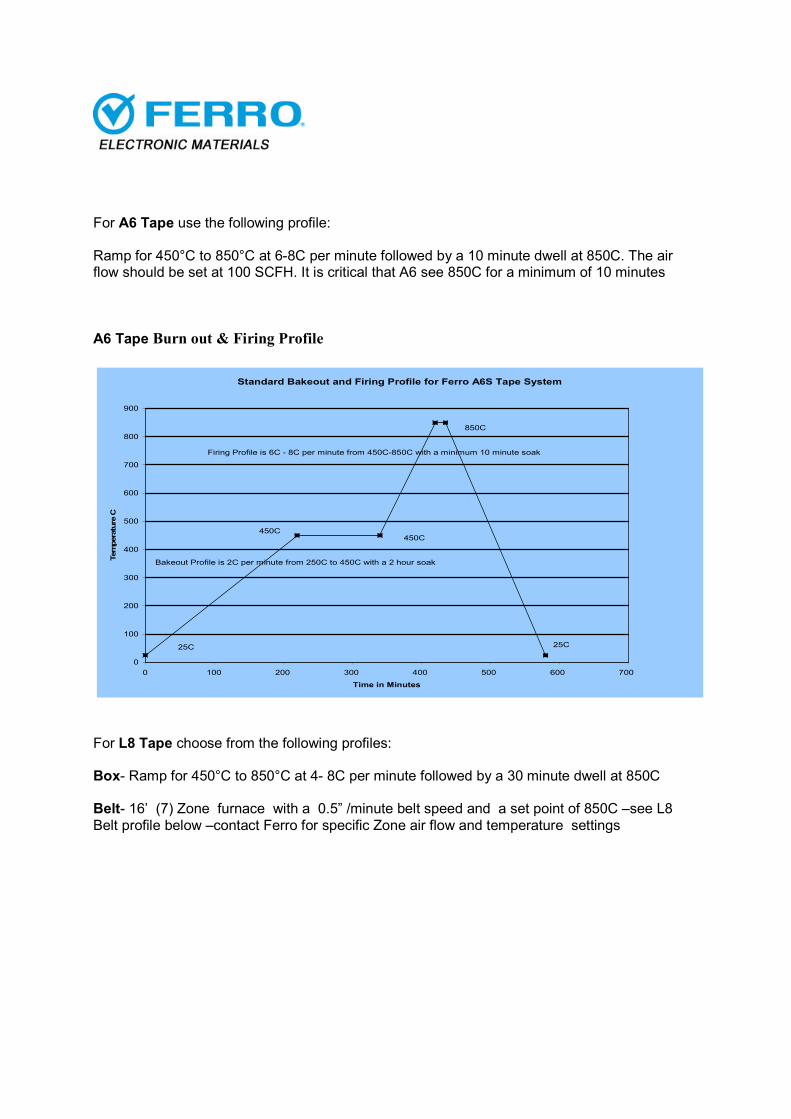
For A6 Tape use the following profile:
Ramp for 450°C to 850°C at 6-8C per minute followed by a 10 minute dwell at 850C. The airflow should be set at 100 SCFH. It is critical that A6 see 850C for a minimum of 10 minutes
A6 Tape Burn out & Firing Profile
Standard Bakeout and Firing Profile for Ferro A6S Tape System
0
100
200
300
400
500
600
700
800
900
0 100 200 300 400 500 600 700
Time in Minutes
Tem
pera
ture
C
450C450C
850C
25C25C
Bakeout Profile is 2C per minute from 250C to 450C with a 2 hour soak
Firing Profile is 6C - 8C per minute from 450C-850C with a minimum 10 minute soak
For L8 Tape choose from the following profiles:
Box- Ramp for 450°C to 850°C at 4- 8C per minute followed by a 30 minute dwell at 850C
Belt- 16’ (7) Zone furnace with a 0.5” /minute belt speed and a set point of 850C –see L8Belt profile below –contact Ferro for specific Zone air flow and temperature settings

L8 Tape Burn out & Firing Profile Box Furnace
Standard Bakeout and Firing Profile for Ferro L8- Box Kiln
0
100
200
300
400
500
600
700
800
900
0 100 200 300 400 500 600
Time in Minutes
Tem
pera
ture
C
450C
Bakeout Profile is 1C* per minute from 25C to 450C with a 2 hour soak
Firing Ramp Rate is 4C - 8C per minute from 450C - 850C with a 30 minute soak
* Bakeout ramp adjusted to 1C /min for Thicker Parts > 50-mils
Parts less than 50 mils can generally use a 2C ramp for Bakeout depending
upon metal loading
L8 Tape Burn out & Firing Profile Belt Furnace
L8 Belt Profile
0
100
200
300
400
500
600
700
800
900
0 50 100 150 200 250 300 350 400 450
Time Minutes
Tem
pera
ture
C
1.15 FIRING
RECOMMENDED SETTTERS
Fused quartz for either L8 or A6 . Bare alumina setters are ok for L8 but should not be used forA6M. In some cases Zirconia felt is better for full coverage ground plane metallization parts toimprove air flow and reduce hot spots and ultimately warpage.
RECOMMENDED SUPPLIERS Fused Quartz GE 124, 16 micro inch surface: Behm Quartz Industries,
www.behmquartz.com 800.543.7875 Zirconia Felt: Zicar Fibrous Ceramics, Part No. ZYF-50, Tel: 800.245.2562 Alumina Setters, 96% Alumina, Coorstek www.coorstek.com
1.16 CLEANING
There is no cleaning solution for tape. Particulates are typically removed with an anti-staticbrush. We recommend using only reagent grade acetone for cleaning fired parts.
LTCC DESIGNRECOMMENDATIONS
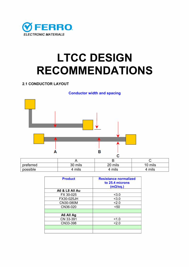
2.1 CONDUCTOR LAYOUT
Conductor width and spacing
A B Cpreferred 30 mils 20 mils 10 milspossible 4 mils 4 mils 4 mils
Product Resistance normalizedto 25.4 microns
(mΩ/sq.)A6 & L8 All Au
FX 30-025 <3.0FX30-025JH <3.0CN30-080M <2.0CN36-020 <50
A6 All AgCN 33-391 <1.0CN33-398 <2.0

L8 All AgCN33- 498 Ag <2.0CN33-495 Ag <2.0
Conductor to edge ofsubstrate dimension
Green Cut Parts Sawed Scribe and Break Post FiredA Surface A Buried A Surface A Buried A Surface A Surface
20 mils 20 mils 20 mils 20 mils 20 mils 20 mils
IC Bond Pad Area
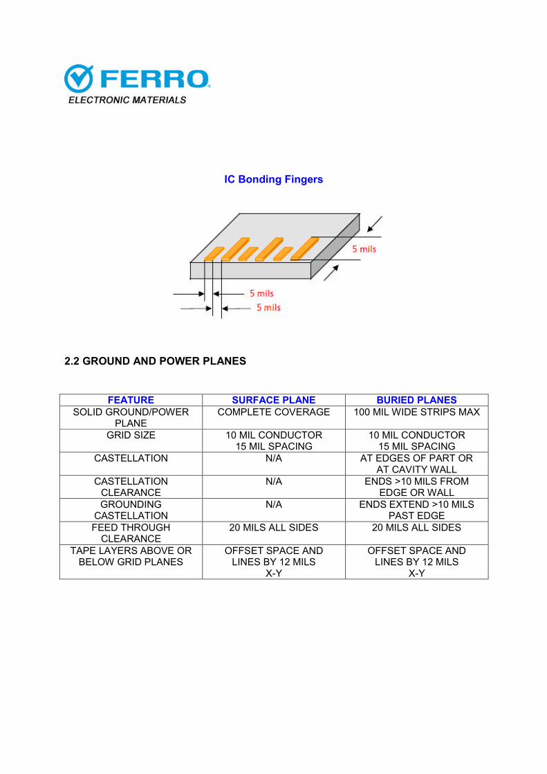
IC Bonding Fingers
2.2 GROUND AND POWER PLANES
FEATURE SURFACE PLANE BURIED PLANESSOLID GROUND/POWER
PLANECOMPLETE COVERAGE 100 MIL WIDE STRIPS MAX
GRID SIZE 10 MIL CONDUCTOR15 MIL SPACING
10 MIL CONDUCTOR15 MIL SPACING
CASTELLATION N/A AT EDGES OF PART ORAT CAVITY WALL
CASTELLATIONCLEARANCE
N/A ENDS >10 MILS FROMEDGE OR WALL
GROUNDINGCASTELLATION
N/A ENDS EXTEND >10 MILSPAST EDGE
FEED THROUGHCLEARANCE
20 MILS ALL SIDES 20 MILS ALL SIDES
TAPE LAYERS ABOVE ORBELOW GRID PLANES
OFFSET SPACE ANDLINES BY 12 MILS
X-Y
OFFSET SPACE ANDLINES BY 12 MILS
X-Y

2.3 CAVITIES

2.4 ELECTRICAL VIAS
Electrical via to edge of substrate.
ThicknessVia
DiameterA
MinRecommendedPunch Method
2 mil >10 mil 25 mil Punch4-10 20 mil Punch
<4 mil 20 mil Punch5 mil >10 mil 25 mil Punch
4-10 20 mil Punch<4 mil 20 mil Punch
10 mil >10 mil 25 mil Punch4-10 20 mil Punch
<4 mil 20 mil Punch
2.5 RF VIAS
Designs requiring high frequency lines and controlled impedance lines may require buriedcoaxial type shielding which is accomplished by placing vias parallel to the controlled linesthrough-out the shielded cross sectional area. RF vias may be paced as close as 2 mils apart(horizontal displacement on layers) as long as they are electrically common to each other. RFvias may also be stacked if required as adjacent layers) as long as they are electrically commonto each other. RF vias may also be stacked if required as long as they maintain 2 via diameterspitch minimum. See diagram below.
RF VIAS Top View of Vias

2.6 THERMAL VIAS
Dimensions of Thermal Via and Catch Pad
ProductThermal Conductivity
(W/m-k)Thermal
ResistanceA6CN 30-078 (Au) >50 <15CN33-343 (Ag) 100 <15CN33-407 (Ag) 100 <15CN39-005 (Transition) N/A N/A
L8CN33-493 (Ag) N/A N/ACN 30-078 (Au) >50 <15
NOTES:1.) Thermal via arrays can have catch pad planes covering the entire array oneach layer of standard catch pads.2.) All thermal via catch pads must be square.

Thermal Hexagonal Via Pattern: Six mil vias only
Thermal Rectangular Via Pattern: 6 or 10 mil vias
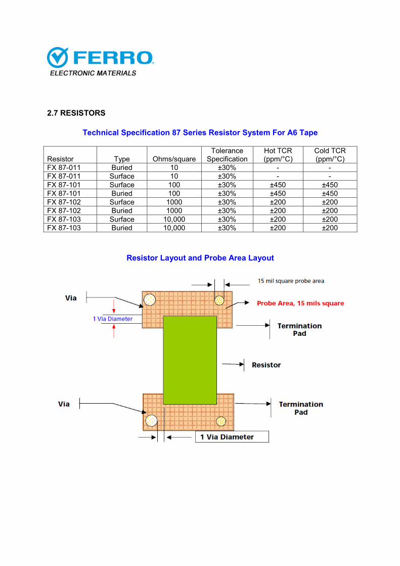
2.7 RESISTORS
Technical Specification 87 Series Resistor System For A6 Tape
Resistor Type Ohms/squareTolerance
SpecificationHot TCR(ppm/°C)
Cold TCR(ppm/°C)
FX 87-011 Buried 10 ±30% - -FX 87-011 Surface 10 ±30% - -FX 87-101 Surface 100 ±30% ±450 ±450FX 87-101 Buried 100 ±30% ±450 ±450FX 87-102 Surface 1000 ±30% ±200 ±200FX 87-102 Buried 1000 ±30% ±200 ±200FX 87-103 Surface 10,000 ±30% ±200 ±200FX 87-103 Buried 10,000 ±30% ±200 ±200
Resistor Layout and Probe Area Layout

Resistor to conductor termination overlaps for surface and buried resistors
LayoutMinimum Spacing
(mils)Maximum Spacing
(mils)A 10 15B 15 20C 10 10

2.7 Resistors-cont.
Blending of the 87 Series
Blend curve for 87-101Series Resistor Material with
% Additions of 87-011 (40 x 40 mil resistor)
0
20
40
60
80
100
120
0 20 40 60 80 100
Percent by weight of 87-011
Oh
ms