ltc4088 - high efficiency battery charger/usb power manager
TRANSCRIPT
LTC4088
14088fb
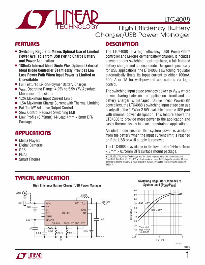
Typical applicaTion
FeaTures DescripTion
High Efficiency Battery Charger/USB Power Manager
The LTC®4088 is a high efficiency USB PowerPath™ controller and Li-Ion/Polymer battery charger. It includes a synchronous switching input regulator, a full-featured battery charger and an ideal diode. Designed specifically for USB applications, the LTC4088’s switching regulator automatically limits its input current to either 100mA, 500mA or 1A for wall-powered applications via logic control.
The switching input stage provides power to VOUT where power sharing between the application circuit and the battery charger is managed. Unlike linear PowerPath controllers, the LTC4088’s switching input stage can use nearly all of the 0.5W or 2.5W available from the USB port with minimal power dissipation. This feature allows the LTC4088 to provide more power to the application and eases thermal issues in space-constrained applications.
An ideal diode ensures that system power is available from the battery when the input current limit is reached or if the USB or wall supply is removed.
The LTC4088 is available in the low profile 14-lead 4mm × 3mm × 0.75mm DFN surface mount package.L, LT, LTC, LTM, Linear Technology and the Linear logo are registered trademarks and PowerPath, Bat-Track and ThinSOT are trademarks of Linear Technology Corporation. All other trademarks are the property of their respective owners. Protected by U.S. Patents, including 6522118.
applicaTions
n Switching Regulator Makes Optimal Use of Limited Power Available from USB Port to Charge Battery and Power Application
n 180mΩ Internal Ideal Diode Plus Optional External Ideal Diode Controller Seamlessly Provides Low Loss Power Path When Input Power is Limited or Unavailable
n Full Featured Li-Ion/Polymer Battery Chargern VBUS Operating Range: 4.25V to 5.5V (7V Absolute
Maximum—Transient)n 1.2A Maximum Input Current Limitn 1.5A Maximum Charge Current with Thermal Limitingn Bat-Track™ Adaptive Output Controln Slew Control Reduces Switching EMIn Low Profile (0.75mm) 14-Lead 4mm × 3mm DFN
Package
n Media Playersn Digital Camerasn GPSn PDAsn Smart Phones
High Efficiency Battery Charger/USB Power ManagerSwitching Regulator Efficiency to
System Load (POUT/PBUS)
VBUS VOUT
10µF
WALL
USB
0.1µF
1µF
3.3V 10µF
SYSTEMLOAD
2.94k 499Ω8.2Ω
4088 TA01a
CLPROG PROG
LTC4088
C/X GND
SW
3.3µH
NTC
D0D1D2CHRGLDO3V3
GATEBAT
+Li-Ion
IOUT (A)0.01
0
EFFI
CIEN
CY (%
)
20
40
60
80
0.1 1
4088 TA01b
100
10
30
50
70
90
BAT = 4.2V
BAT = 3.3V
VBUS = 5VIBAT = 0mA10x MODE

LTC4088
24088fb
pin conFiguraTionabsoluTe MaxiMuM raTings
VBUS (Transient) t < 1ms, Duty Cycle < 1% .. –0.3V to 7VVBUS (Static), BAT, CHRG, NTC, D0, D1, D2 .......................................................... –0.3V to 6VICLPROG ....................................................................3mAIPROG, IC/X ................................................................2mAILDO3V3 ...................................................................30mAICHRG ......................................................................75mAIOUT ............................................................................2AISW ..............................................................................2AIBAT ............................................................................2AMaximum Operating Junction Temperature .......... 125°COperating Temperature Range .................–40°C to 85°CStorage Temperature Range .................. –65°C to 125°C
(Note 1)
1
2
3
4
5
6
7
14
13
12
11
10
9
8
D1
D0
SW
VBUSVOUT
BAT
GATE
NTC
CLPROG
LDO3V3
D2
C/X
PROG
CHRG
TOP VIEW
15
DE PACKAGE14-LEAD (4mm × 3mm) PLASTIC DFN
TJMAX = 125°C, θJA = 37°C/W EXPOSED PAD (PIN 15) IS GND, MUST BE SOLDERED TO PCB
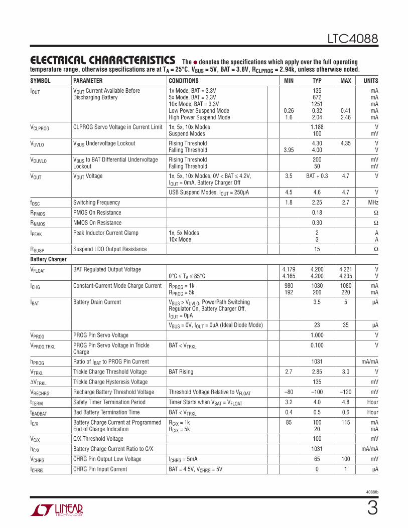
elecTrical characTerisTics The l denotes the specifications which apply over the full operating temperature range, otherwise specifications are at TA = 25°C. VBUS = 5V, BAT = 3.8V, RCLPROG = 2.94k, unless otherwise noted.
SYMBOL PARAMETER CONDITIONS MIN TYP MAX UNITS
Input Power Supply
VBUS Input Supply Voltage l 4.35 5.5 V
IBUS(LIM) Total Input Current 1x Mode 5x Mode 10x Mode Low Power Suspend Mode High Power Suspend Mode
l
l
l
l
l
92 445 815 0.32 1.6
97 470 877 0.39 2.05
100 500
1000 0.50 2.5
mA mA mA mA mA
IBUSQ (Note 4) Input Quiescent Current 1x Mode 5x Mode 10x Mode Low Power Suspend Mode High Power Suspend Mode
6 14 14
0.038 0.038
mA mA mA mA mA
hCLPROG (Note 4) Ratio of Measured VBUS Current to CLPROG Program Current
1x Mode 5x Mode 10x Mode Low Power Suspend Mode High Power Suspend Mode
224 1133 2140 11.3 59.4
mA/mA mA/mA mA/mA mA/mA mA/mA
orDer inForMaTionLEAD FREE FINISH TAPE AND REEL PART MARKING PACKAGE DESCRIPTION TEMPERATURE RANGE
LTC4088EDE#PBF LTC4088EDE#TRPBF 4088 14-Lead (4mm × 3mm) Plastic DFN –40°C to 85°C
Consult LTC Marketing for parts specified with wider operating temperature ranges. Consult LTC Marketing for information on nonstandard lead based finish parts.For more information on lead free part marking, go to: http://www.linear.com/leadfree/ For more information on tape and reel specifications, go to: http://www.linear.com/tapeandreel/
LTC4088
34088fb
elecTrical characTerisTics The l denotes the specifications which apply over the full operating temperature range, otherwise specifications are at TA = 25°C. VBUS = 5V, BAT = 3.8V, RCLPROG = 2.94k, unless otherwise noted.
SYMBOL PARAMETER CONDITIONS MIN TYP MAX UNITS
IOUT VOUT Current Available Before Discharging Battery
1x Mode, BAT = 3.3V 5x Mode, BAT = 3.3V 10x Mode, BAT = 3.3V Low Power Suspend Mode High Power Suspend Mode
0.26 1.6
135 672
1251 0.32 2.04
0.41 2.46
mA mA mA mA mA
VCLPROG CLPROG Servo Voltage in Current Limit 1x, 5x, 10x Modes Suspend Modes
1.188 100
V mV
VUVLO VBUS Undervoltage Lockout Rising Threshold Falling Threshold
3.95
4.30 4.00
4.35 V V
VDUVLO VBUS to BAT Differential Undervoltage Lockout
Rising Threshold Falling Threshold
200 50
mV mV
VOUT VOUT Voltage 1x, 5x, 10x Modes, 0V < BAT ≤ 4.2V, IOUT = 0mA, Battery Charger Off
3.5 BAT + 0.3 4.7 V
USB Suspend Modes, IOUT = 250µA 4.5 4.6 4.7 V
fOSC Switching Frequency 1.8 2.25 2.7 MHz
RPMOS PMOS On Resistance 0.18 Ω
RNMOS NMOS On Resistance 0.30 Ω
IPEAK Peak Inductor Current Clamp 1x, 5x Modes 10x Mode
2 3
A A
RSUSP Suspend LDO Output Resistance 15 Ω
Battery Charger
VFLOAT BAT Regulated Output Voltage 0°C ≤ TA ≤ 85°C
4.179 4.165
4.200 4.200
4.221 4.235
V V
ICHG Constant-Current Mode Charge Current RPROG = 1k RPROG = 5k
980 192
1030 206
1080 220
mA mA
IBAT Battery Drain Current VBUS > VUVLO, PowerPath Switching Regulator On, Battery Charger Off, IOUT = 0µA
3.5 5 µA
VBUS = 0V, IOUT = 0µA (Ideal Diode Mode) 23 35 µA
VPROG PROG Pin Servo Voltage 1.000 V
VPROG,TRKL PROG Pin Servo Voltage in Trickle Charge
BAT < VTRKL 0.100 V
hPROG Ratio of IBAT to PROG Pin Current 1031 mA/mA
VTRKL Trickle Charge Threshold Voltage BAT Rising 2.7 2.85 3.0 V
ΔVTRKL Trickle Charge Hysteresis Voltage 135 mV
VRECHRG Recharge Battery Threshold Voltage Threshold Voltage Relative to VFLOAT –80 –100 –120 mV
tTERM Safety Timer Termination Period Timer Starts when VBAT = VFLOAT 3.2 4.0 4.8 Hour
tBADBAT Bad Battery Termination Time BAT < VTRKL 0.4 0.5 0.6 Hour
IC/X Battery Charge Current at Programmed End of Charge Indication
RC/X = 1k RC/X = 5k
85 100 20
115 mA mA
VC/X C/X Threshold Voltage 100 mV
hC/X Battery Charge Current Ratio to C/X 1031 mA/mA
VCHRG CHRG Pin Output Low Voltage ICHRG = 5mA 65 100 mV
ICHRG CHRG Pin Input Current BAT = 4.5V, VCHRG = 5V 0 1 µA
LTC4088
44088fb
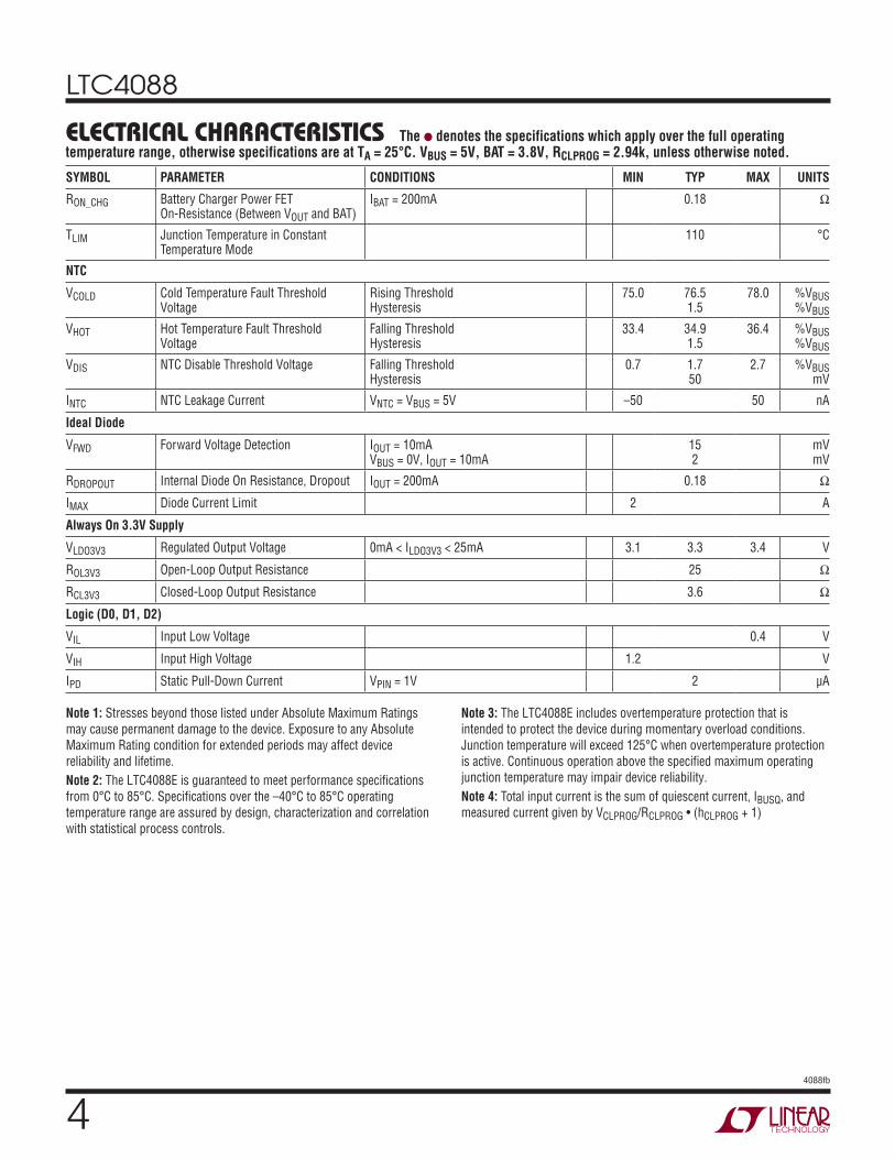
elecTrical characTerisTics The l denotes the specifications which apply over the full operating temperature range, otherwise specifications are at TA = 25°C. VBUS = 5V, BAT = 3.8V, RCLPROG = 2.94k, unless otherwise noted.
SYMBOL PARAMETER CONDITIONS MIN TYP MAX UNITS
RON_CHG Battery Charger Power FET On-Resistance (Between VOUT and BAT)
IBAT = 200mA 0.18 Ω
TLIM Junction Temperature in Constant Temperature Mode
110 °C
NTC
VCOLD Cold Temperature Fault Threshold Voltage
Rising Threshold Hysteresis
75.0 76.5 1.5
78.0 %VBUS %VBUS
VHOT Hot Temperature Fault Threshold Voltage
Falling Threshold Hysteresis
33.4 34.9 1.5
36.4 %VBUS %VBUS
VDIS NTC Disable Threshold Voltage Falling Threshold Hysteresis
0.7 1.7 50
2.7 %VBUS mV
INTC NTC Leakage Current VNTC = VBUS = 5V –50 50 nA
Ideal Diode
VFWD Forward Voltage Detection IOUT = 10mA VBUS = 0V, IOUT = 10mA
15 2
mV mV
RDROPOUT Internal Diode On Resistance, Dropout IOUT = 200mA 0.18 Ω
IMAX Diode Current Limit 2 A
Always On 3.3V Supply
VLDO3V3 Regulated Output Voltage 0mA < ILDO3V3 < 25mA 3.1 3.3 3.4 V
ROL3V3 Open-Loop Output Resistance 25 Ω
RCL3V3 Closed-Loop Output Resistance 3.6 Ω
Logic (D0, D1, D2)
VIL Input Low Voltage 0.4 V
VIH Input High Voltage 1.2 V
IPD Static Pull-Down Current VPIN = 1V 2 µA
Note 1: Stresses beyond those listed under Absolute Maximum Ratings may cause permanent damage to the device. Exposure to any Absolute Maximum Rating condition for extended periods may affect device reliability and lifetime.Note 2: The LTC4088E is guaranteed to meet performance specifications from 0°C to 85°C. Specifications over the –40°C to 85°C operating temperature range are assured by design, characterization and correlation with statistical process controls.
Note 3: The LTC4088E includes overtemperature protection that is intended to protect the device during momentary overload conditions. Junction temperature will exceed 125°C when overtemperature protection is active. Continuous operation above the specified maximum operating junction temperature may impair device reliability.Note 4: Total input current is the sum of quiescent current, IBUSQ, and measured current given by VCLPROG/RCLPROG • (hCLPROG + 1)
LTC4088
54088fb
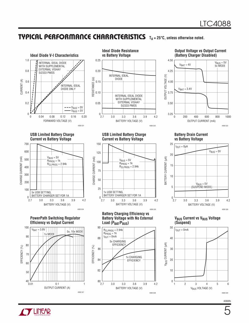
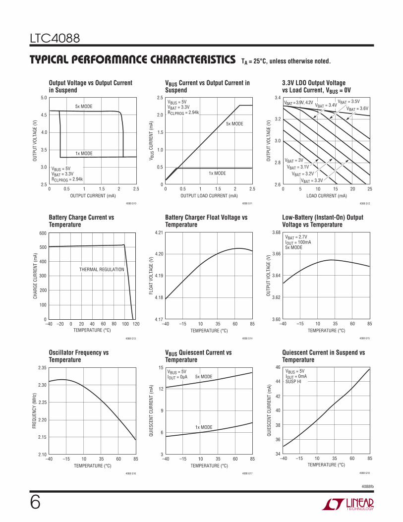
Typical perForMance characTerisTics TA = 25°C, unless otherwise noted.
PowerPath Switching Regulator Efficiency vs Output Current
Battery Charging Efficiency vs Battery Voltage with No External Load (PBAT/PBUS)
VBUS Current vs VBUS Voltage (Suspend)
Ideal Diode V-I CharacteristicsIdeal Diode Resistance vs Battery Voltage
Output Voltage vs Output Current (Battery Charger Disabled)
USB Limited Battery Charge Current vs Battery Voltage
Battery Drain Current vs Battery Voltage
USB Limited Battery Charge Current vs Battery Voltage
FORWARD VOLTAGE (V)0
CURR
ENT
(A)
0.6
0.8
1.0
0.16
4088 G01
0.4
0.2
00.04 0.08 0.12 0.20
INTERNAL IDEAL DIODEWITH SUPPLEMENTALEXTERNAL VISHAYSi2333 PMOS
INTERNAL IDEALDIODE ONLY
VBUS = 0VVBUS = 5V
BATTERY VOLTAGE (V)2.7
RESI
STAN
CE (Ω
)
0.15
0.20
0.25
3.9
4088 G02
0.10
0.05
03.0 3.3 3.6 4.2
INTERNAL IDEAL DIODEWITH SUPPLEMENTAL
EXTERNAL VISHAYSi2333 PMOS
INTERNAL IDEALDIODE
OUTPUT CURRENT (mA)0
OUTP
UT V
OLTA
GE (V
)
4.00
4.25
4.50
800
4088 G03
3.75
3.50
3.25200 400 600 1000
VBAT = 4V
VBAT = 3.4V
VBUS = 5V5x MODE
BATTERY VOLTAGE (V)2.7
500
600
700
3.9
4088 G04
400
300
3.0 3.3 3.6 4.2
200
100
0
CHAR
GE C
URRE
NT (m
A) VBUS = 5VRPROG = 1kRCLPROG = 2.94k
5x USB SETTING,BATTERY CHARGER SET FOR 1A
BATTERY VOLTAGE (V)2.7
0
CHAR
GE C
URRE
NT (m
A)
25
50
75
100
125
150
3.0 3.3 3.6 3.9
4088 G05
4.2
VBUS = 5VRPROG = 1kRCLPROG = 2.94k
1x USB SETTING,BATTERY CHARGER SET FOR 1A
BATTERY VOLTAGE (V)2.7
BATT
ERY
CURR
ENT
(µA)
15
20
25
3.9
4088 G06
10
5
03.0 3.3 3.6 4.2
VBUS = 0V
VBUS = 5V(SUSPEND MODE)
IOUT = 0µA
OUTPUT CURRENT (A)0.01
40
EFFI
CIEN
CY (%
)
50
60
70
80
100
0.1 1
4088 G07
90
5x, 10x MODE1x MODE
VBAT = 3.8V
VBUS VOLTAGE (V)1
V BUS
CUR
RENT
(µA)
30
40
50
5
4088 G09
20
10
02 3 4 6
IOUT = 0mA
BATTERY VOLTAGE (V)2.7
EFFI
CIEN
CY (%
)
86
88
90
3.9
4088 G08
84
82
803.0 3.3 3.6 4.2
RCLPROG = 2.94kRPROG = 1kIOUT = 0mA
5x CHARGINGEFFICIENCY
1x CHARGINGEFFICIENCY
LTC4088
64088fb
Typical perForMance characTerisTics TA = 25°C, unless otherwise noted.
Oscillator Frequency vs Temperature
VBUS Quiescent Current vs Temperature
Quiescent Current in Suspend vs Temperature
Battery Charge Current vs Temperature
Battery Charger Float Voltage vs Temperature
Low-Battery (Instant-On) Output Voltage vs Temperature
Output Voltage vs Output Current in Suspend
VBUS Current vs Output Current in Suspend
3.3V LDO Output Voltage vs Load Current, VBUS = 0V
OUTPUT CURRENT (mA)0
OUTP
UT V
OLTA
GE (V
)
4.0
4.5
5.0
2
4088 G10
3.5
3.0
2.50.5 1 1.5 2.5
5x MODE
1x MODE
VBUS = 5VVBAT = 3.3VRCLPROG = 2.94k
OUTPUT LOAD CURRENT (mA)0
V BUS
CUR
RENT
(mA)
1.5
2.0
2.5
2
4088 G11
1.0
0.5
00.5 1 1.5 2.5
5x MODE
1x MODE
VBUS = 5VVBAT = 3.3VRCLPROG = 2.94k
LOAD CURRENT (mA)0
OUTP
UT V
OLTA
GE (V
)
3.0
3.2
20
4088 G12
2.8
2.65 10 15 25
3.4
VBAT = 3VVBAT = 3.1V
VBAT = 3.2VVBAT = 3.3V
VBAT = 3.6VVBAT = 3.5V
VBAT = 3.4VVBAT = 3.9V, 4.2V
TEMPERATURE (°C)–40
0
CHAR
GE C
URRE
NT (m
A)
100
200
300
400
0 40 80 120
4088 G13
500
600
–20 20 60 100
THERMAL REGULATION
TEMPERATURE (°C)–40
FLOA
T VO
LTAG
E (V
)
4.19
4.20
60
4088 G14
4.18
4.17–15 10 35 85
4.21
TEMPERATURE (°C)–40
OUTP
UT V
OLTA
GE (V
)
3.64
3.66
60
4088 G15
3.62
3.60–15 10 35 85
3.68VBAT = 2.7VIOUT = 100mA5x MODE
TEMPERATURE (°C)–40
FREQ
UENC
Y (M
Hz)
2.25
2.30
2.35
60
4088 G16
2.20
2.15
2.10–15 10 35 85
TEMPERATURE (°C)–40
QUIE
SCEN
T CU
RREN
T (m
A)
9
12
60
4088 G17
6
3–15 10 35 85
15VBUS = 5VIOUT = 0µA 5x MODE
1x MODE
TEMPERATURE (°C)–40
34
QUIE
SCEN
T CU
RREN
T (m
A)
36
38
40
42
44
46
–15 10 35 60
4088 G18
85
VBUS = 5VIOUT = 0mASUSP HI
LTC4088
74088fb
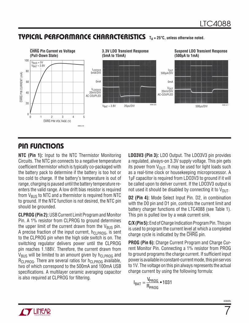
Typical perForMance characTerisTics TA = 25°C, unless otherwise noted.
CHRG Pin Current vs Voltage (Pull-Down State)
3.3V LDO Transient Response (5mA to 15mA)
Suspend LDO Transient Response (500µA to 1mA)
CHRG PIN VOLTAGE (V)0
CHRG
PIN
CUR
RENT
(mA)
60
80
100
4
4088 G19
40
20
01 2 3 5
VBUS = 5VVBAT = 3.8V
ILDO3V35mA/DIV
0mA
20µs/DIVVBAT = 3.8V 4088 G20
VLDO3V320mV/DIV
AC COUPLED
IOUT500µA/DIV
0mA
500µs/DIV 4088 G21
VOUT20mV/DIV
AC-COUPLED
pin FuncTionsNTC (Pin 1): Input to the NTC Thermistor Monitoring Circuits. The NTC pin connects to a negative temperature coefficient thermistor which is typically co-packaged with the battery pack to determine if the battery is too hot or too cold to charge. If the battery’s temperature is out of range, charging is paused until the battery temperature re-enters the valid range. A low drift bias resistor is required from VBUS to NTC and a thermistor is required from NTC to ground. If the NTC function is not desired, the NTC pin should be grounded.
CLPROG (Pin 2): USB Current Limit Program and Monitor Pin. A 1% resistor from CLPROG to ground determines the upper limit of the current drawn from the VBUS pin. A precise fraction of the input current, hCLPROG, is sent to the CLPROG pin when the high side switch is on. The switching regulator delivers power until the CLPROG pin reaches 1.188V. Therefore, the current drawn from VBUS will be limited to an amount given by hCLPROG and RCLPROG. There are several ratios for hCLPROG available, two of which correspond to the 500mA and 100mA USB specifications. A multilayer ceramic averaging capacitor is also required at CLPROG for filtering.
LDO3V3 (Pin 3): LDO Output. The LDO3V3 pin provides a regulated, always-on 3.3V supply voltage. This pin gets its power from VOUT. It may be used for light loads such as a real-time clock or housekeeping microprocessor. A 1µF capacitor is required from LDO3V3 to ground if it will be called upon to deliver current. If the LDO3V3 output is not used it should be disabled by connecting it to VOUT.
D2 (Pin 4): Mode Select Input Pin. D2, in combination with the D0 pin and D1 pin, controls the current limit and battery charger functions of the LTC4088 (see Table 1). This pin is pulled low by a weak current sink.
C/X (Pin 5): End of Charge Indication Program Pin. This pin is used to program the current level at which a completed charge cycle is indicated by the CHRG pin.
PROG (Pin 6): Charge Current Program and Charge Cur-rent Monitor Pin. Connecting a 1% resistor from PROG to ground programs the charge current. If sufficient input power is available in constant-current mode, this pin servos to 1V. The voltage on this pin always represents the actual charge current by using the following formula:
IBAT =
VPROGRPROG
• 1031

LTC4088
84088fb
pin FuncTionsCHRG (Pin 7): Open-Drain Charge Status Output. The CHRG pin indicates the status of the battery charger. Four possible states are represented by CHRG: charging, not charging (or float charge current less than programmed end of charge indication current), unresponsive battery and battery temperature out of range. CHRG is modulated at 35kHz and switches between a low and a high duty cycle for easy recognition by either humans or microprocessors. CHRG requires a pull-up resistor and/or LED to provide indication.
GATE (Pin 8): Ideal Diode Amplifier Output. This pin con-trols the gate of an optional external P-channel MOSFET transistor used to supplement the internal ideal diode. The source of the P-channel MOSFET should be connected to VOUT and the drain should be connected to BAT.
BAT (Pin 9): Single Cell Li-Ion Battery Pin. Depending on available power and load, a Li-Ion battery on BAT will either deliver system power to VOUT through the ideal diode or be charged from the battery charger.
VOUT (Pin 10): Output voltage of the switching PowerPath controller and input voltage of the battery charger. The majority of the portable product should be powered from VOUT. The LTC4088 will partition the available power be-tween the external load on VOUT and the internal battery charger. Priority is given to the external load and any extra power is used to charge the battery. An ideal diode from
BAT to VOUT ensures that VOUT is powered even if the load exceeds the allotted power from VBUS or if the VBUS power source is removed. VOUT should be bypassed with a low impedance multilayer ceramic capacitor.
VBUS (Pin 11): Input voltage for the switching PowerPath controller. VBUS will usually be connected to the USB port of a computer or a DC output wall adapter. VBUS should be bypassed with a low impedance multilayer ceramic capacitor.
SW (Pin 12): The SW pin delivers power from VBUS to VOUT via the step-down switching regulator. An inductor should be connected from SW to VOUT. See the Applica-tions Information section for a discussion of inductance value and current rating.
D0 (Pin 13): Mode Select Input Pin. D0, in combination with the D1 pin and the D2 pin, controls the current limit and battery charger functions of the LTC4088 (see Table 1). This pin is pulled low by a weak current sink.
D1 (Pin 14): Mode Select Input Pin. D1, in combination with the D0 pin and the D2 pin, controls the current limit and battery charger functions of the LTC4088 (see Table 1). This pin is pulled low by a weak current sink.
Exposed Pad (Pin 15): GND. Must be soldered to the PCB to provide a low electrical and thermal impedance connection to ground.
LTC4088
94088fb
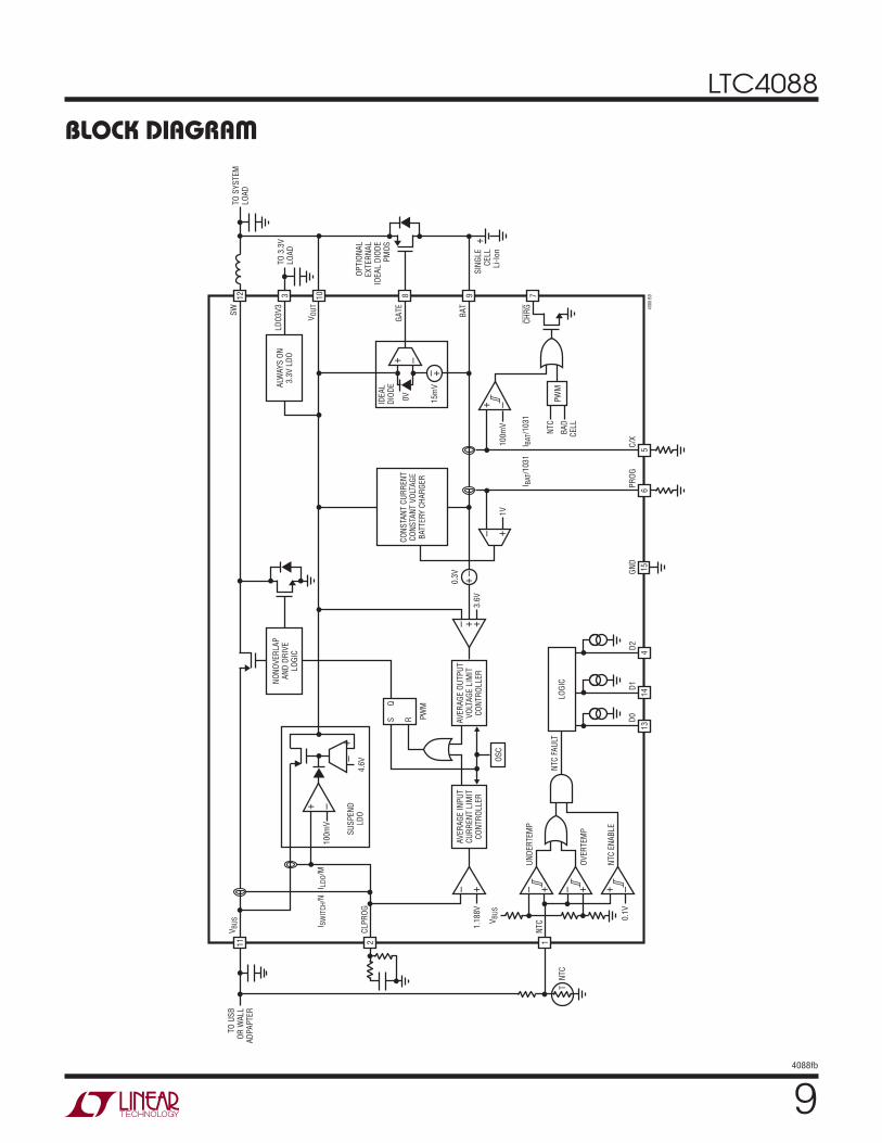
block DiagraM
13
1
+ –
+ –
+–+–
+–
+–
+ –
0.1V
UNDE
RTEM
P
AVER
AGE
INPU
TCU
RREN
T LI
MIT
CONT
ROLL
ER
OVER
TEM
P
NTCV B
US
NTC
T
2CL
PROG
11V B
US
NTC
FAUL
T
D1
NTC
ENAB
LE
14D2 4
D0
LOGI
C
1.18
8V
+–
++–
AVER
AGE
OUTP
UTVO
LTAG
E LI
MIT
CONT
ROLL
ER
OSC
PWM
S PWM
4.6V
100m
V
SUSP
END
LDO
I LDO
/MI S
WIT
CH/N
TO U
SBOR
WAL
LAD
PAPT
ER
Q
R
3.6V
0.3V
1V10
0mV
NTC
4088
BD
I BAT
/103
1I B
AT/1
031
+–
+ –
PROG
6GN
D15
5C/X
79
BAD
CELL
CHRGBA
T
SING
LECE
LLLi
-Ion
OPTI
ONAL
EXTE
RNAL
IDEA
L DI
ODE
PMOS
8GA
TE
10V O
UT
3LD
O3V3
TO 3
.3V
LOAD
TO S
YSTE
MLO
AD
CONS
TANT
CUR
RENT
CONS
TANT
VOL
TAGE
BATT
ERY
CHAR
GER
+–
0V 15m
V
IDEA
L DI
ODE
12SW
ALW
AYS
ON3.
3V L
DO
NONO
VERL
APAN
D DR
IVE
LOGI
C
+
LTC4088
104088fb
operaTionIntroduction
The LTC4088 includes a PowerPath controller, battery charger, internal ideal diode, optional external ideal diode controller, SUSPEND LDO and an always-on 3.3V LDO. Designed specifically for USB applications, the PowerPath controller incorporates a precision average input current limited step-down switching regulator to make maximum use of the allowable USB power. Because power is con-served, the LTC4088 allows the load current on VOUT to exceed the current drawn by the USB port without exceed-ing the USB load specifications.
The switching regulator and battery charger communicate to ensure that the average input current never exceeds the USB specifications.
The ideal diodes from BAT to VOUT guarantee that ample power is always available to VOUT even if there is insuf-ficient or absent power at VBUS.
To prevent battery drain when a device is connected to a suspended USB port, an LDO from VBUS to VOUT provides either low power or high power suspend current to the application.
Finally, an “always on” LDO provides a regulated 3.3V from VOUT. This LDO will be on at all times and can be used to supply up to 25mA to a system microprocessor.
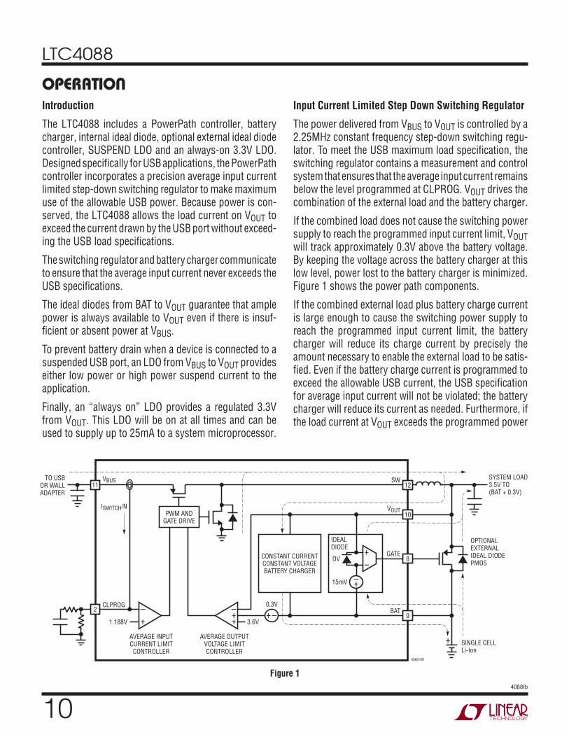
Input Current Limited Step Down Switching Regulator
The power delivered from VBUS to VOUT is controlled by a 2.25MHz constant frequency step-down switching regu-lator. To meet the USB maximum load specification, the switching regulator contains a measurement and control system that ensures that the average input current remains below the level programmed at CLPROG. VOUT drives the combination of the external load and the battery charger.
If the combined load does not cause the switching power supply to reach the programmed input current limit, VOUT will track approximately 0.3V above the battery voltage. By keeping the voltage across the battery charger at this low level, power lost to the battery charger is minimized. Figure 1 shows the power path components.
If the combined external load plus battery charge current is large enough to cause the switching power supply to reach the programmed input current limit, the battery charger will reduce its charge current by precisely the amount necessary to enable the external load to be satis-fied. Even if the battery charge current is programmed to exceed the allowable USB current, the USB specification for average input current will not be violated; the battery charger will reduce its current as needed. Furthermore, if the load current at VOUT exceeds the programmed power
Figure 1
+–
++– 0.3V
1.188V 3.6V
CLPROG
ISWITCH/N
+–
+–15mV
OV
IDEAL DIODE
PWM ANDGATE DRIVE
AVERAGE INPUTCURRENT LIMITCONTROLLER
AVERAGE OUTPUTVOLTAGE LIMITCONTROLLER
CONSTANT CURRENTCONSTANT VOLTAGEBATTERY CHARGER
+–
2
GATE8
VOUT10
SW SYSTEM LOAD3.5V TO(BAT + 0.3V)
OPTIONALEXTERNALIDEAL DIODEPMOS
SINGLE CELLLi-Ion
4088 F01
12
BAT9
VBUSTO USBOR WALLADAPTER
11
+
LTC4088
114088fb
operaTionfrom VBUS, load current will be drawn from the battery via the ideal diodes even when the battery charger is enabled.
The current at CLPROG is a precise fraction of the VBUS current. When a programming resistor and an averaging capacitor are connected from CLPROG to GND, the voltage on CLPROG represents the average input current of the switching regulator. As the input current approaches the programmed limit, CLPROG reaches 1.188V and power delivered by the switching regulator is held constant. Several ratios of current are available which can be set to correspond to USB low and high power modes with a single programming resistor.
The input current limit is programmed by various com-binations of the D0, D1 and D2 pins as shown in Table 1. The switching input regulator can also be deactivated (USB Suspend).
The average input current will be limited by the CLPROG programming resistor according to the following expres-sion:
IVBUS = IBUSQ +
VCLPROGRCLPROG
• hCLPROG + 1( )where IBUSQ is the quiescent current of the LTC4088, VCLPROG is the CLPROG servo voltage in current limit, RCLPROG is the value of the programming resistor and hCLPROG is the ratio of the measured current at VBUS to the sample current delivered to CLPROG. Refer to the Electrical Characteristics table for values of hCLPROG, VCLPROG and IBUSQ. Given worst-case circuit tolerances, the USB specification for the average input current of 1x or 5x mode will not be violated, provided that RCLPROG is 2.94k or greater.
Table 1 shows the available settings for the D0, D1 and D2 pins.
Notice that when D0 is high and D1 is low, the switching regulator is set to a higher current limit for increased charging and power availability at VOUT. These modes will typically be used when there is line power available from a wall adapter.
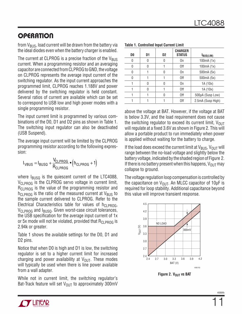
While not in current limit, the switching regulator’s Bat-Track feature will set VOUT to approximately 300mV
above the voltage at BAT. However, if the voltage at BAT is below 3.3V, and the load requirement does not cause the switching regulator to exceed its current limit, VOUT will regulate at a fixed 3.6V as shown in Figure 2. This will allow a portable product to run immediately when power is applied without waiting for the battery to charge.
If the load does exceed the current limit at VBUS, VOUT will range between the no-load voltage and slightly below the battery voltage, indicated by the shaded region of Figure 2. If there is no battery present when this happens, VOUT may collapse to ground.
The voltage regulation loop compensation is controlled by the capacitance on VOUT. An MLCC capacitor of 10µF is required for loop stability. Additional capacitance beyond this value will improve transient response.
Table 1. Controlled Input Current Limit
D0 D1 D2CHARGER STATUS IBUS(LIM)
0 0 0 On 100mA (1x)
0 0 1 Off 100mA (1x)
0 1 0 On 500mA (5x)
0 1 1 Off 500mA (5x)
1 0 0 On 1A (10x)
1 0 1 Off 1A (10x)
1 1 0 Off 500µA (Susp Low)
1 1 1 Off 2.5mA (Susp High)
Figure 2. VOUT vs BAT
BAT (V)2.4
4.5
4.2
3.9
3.6
3.3
3.0
2.7
2.43.3 3.9
4088 F02
2.7 3.0 3.6 4.2
V OUT
(V) NO LOAD
300mV
LTC4088
124088fb
Ideal Diode from BAT to VOUT
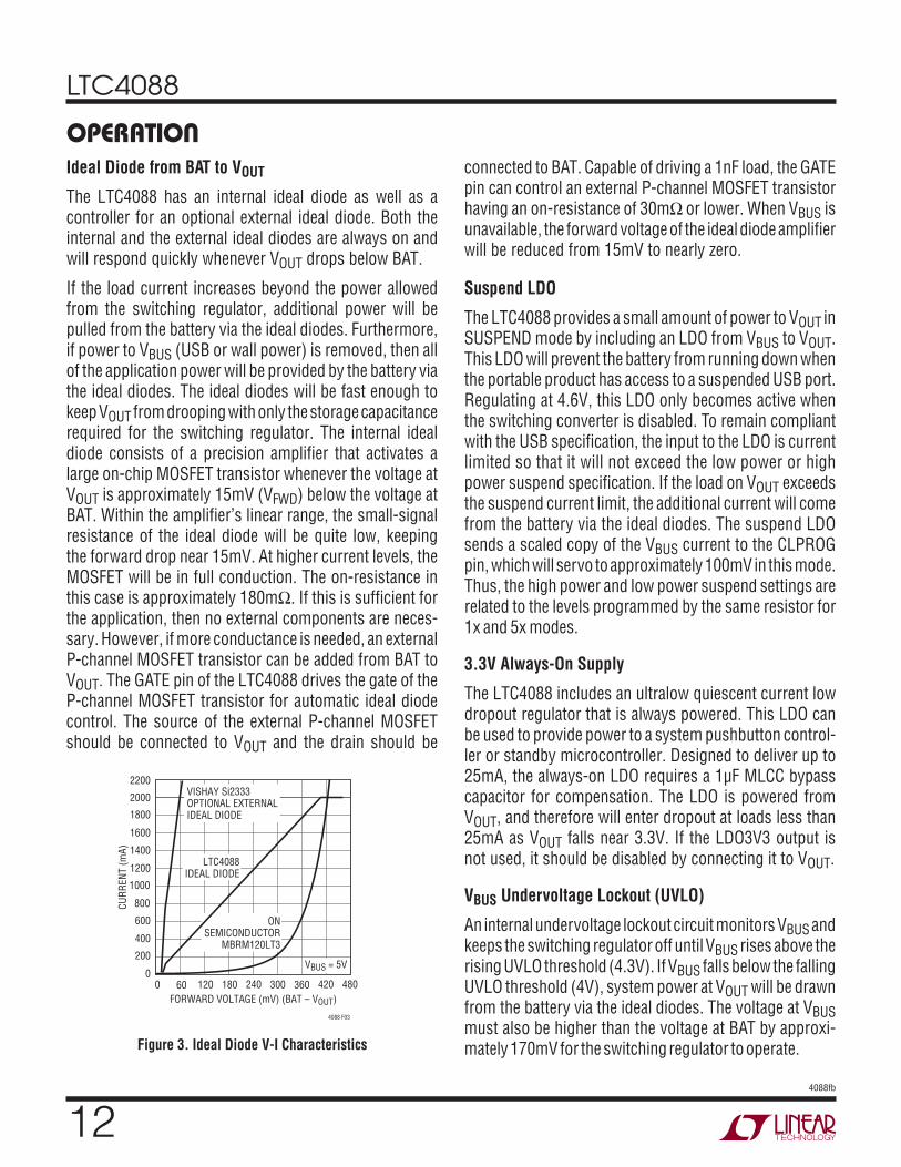
The LTC4088 has an internal ideal diode as well as a controller for an optional external ideal diode. Both the internal and the external ideal diodes are always on and will respond quickly whenever VOUT drops below BAT.
If the load current increases beyond the power allowed from the switching regulator, additional power will be pulled from the battery via the ideal diodes. Furthermore, if power to VBUS (USB or wall power) is removed, then all of the application power will be provided by the battery via the ideal diodes. The ideal diodes will be fast enough to keep VOUT from drooping with only the storage capacitance required for the switching regulator. The internal ideal diode consists of a precision amplifier that activates a large on-chip MOSFET transistor whenever the voltage at VOUT is approximately 15mV (VFWD) below the voltage at BAT. Within the amplifier’s linear range, the small-signal resistance of the ideal diode will be quite low, keeping the forward drop near 15mV. At higher current levels, the MOSFET will be in full conduction. The on-resistance in this case is approximately 180mΩ. If this is sufficient for the application, then no external components are neces-sary. However, if more conductance is needed, an external P-channel MOSFET transistor can be added from BAT to VOUT. The GATE pin of the LTC4088 drives the gate of the P-channel MOSFET transistor for automatic ideal diode control. The source of the external P-channel MOSFET should be connected to VOUT and the drain should be
operaTionconnected to BAT. Capable of driving a 1nF load, the GATE pin can control an external P-channel MOSFET transistor having an on-resistance of 30mΩ or lower. When VBUS is unavailable, the forward voltage of the ideal diode amplifier will be reduced from 15mV to nearly zero.
Suspend LDO
The LTC4088 provides a small amount of power to VOUT in SUSPEND mode by including an LDO from VBUS to VOUT. This LDO will prevent the battery from running down when the portable product has access to a suspended USB port. Regulating at 4.6V, this LDO only becomes active when the switching converter is disabled. To remain compliant with the USB specification, the input to the LDO is current limited so that it will not exceed the low power or high power suspend specification. If the load on VOUT exceeds the suspend current limit, the additional current will come from the battery via the ideal diodes. The suspend LDO sends a scaled copy of the VBUS current to the CLPROG pin, which will servo to approximately 100mV in this mode. Thus, the high power and low power suspend settings are related to the levels programmed by the same resistor for 1x and 5x modes.
3.3V Always-On Supply
The LTC4088 includes an ultralow quiescent current low dropout regulator that is always powered. This LDO can be used to provide power to a system pushbutton control-ler or standby microcontroller. Designed to deliver up to 25mA, the always-on LDO requires a 1µF MLCC bypass capacitor for compensation. The LDO is powered from VOUT, and therefore will enter dropout at loads less than 25mA as VOUT falls near 3.3V. If the LDO3V3 output is not used, it should be disabled by connecting it to VOUT.
VBUS Undervoltage Lockout (UVLO)
An internal undervoltage lockout circuit monitors VBUS and keeps the switching regulator off until VBUS rises above the rising UVLO threshold (4.3V). If VBUS falls below the falling UVLO threshold (4V), system power at VOUT will be drawn from the battery via the ideal diodes. The voltage at VBUS must also be higher than the voltage at BAT by approxi-mately 170mV for the switching regulator to operate.Figure 3. Ideal Diode V-I Characteristics
FORWARD VOLTAGE (mV) (BAT – VOUT)0
CURR
ENT
(mA)
600
1800
2000
2200
120 240 300
4088 F03
200
1400
1000
400
1600
0
1200
800
60 180 360 480420
VISHAY Si2333OPTIONAL EXTERNALIDEAL DIODE
LTC4088IDEAL DIODE
ONSEMICONDUCTOR
MBRM120LT3
VBUS = 5V
LTC4088
134088fb
operaTionBattery Charger
The LTC4088 includes a constant-current/constant-voltage battery charger with automatic recharge, automatic ter-mination by safety timer, low voltage trickle charging, bad cell detection and thermistor sensor input for out of temperature charge pausing.
When a battery charge cycle begins, the battery charger first determines if the battery is deeply discharged. If the battery voltage is below VTRKL, typically 2.85V, an automatic trickle charge feature sets the battery charge current to 10% of the programmed value. If the low voltage persists for more than 1/2 hour, the battery charger automatically terminates and indicates, via the CHRG pin, that the battery was unresponsive.
Once the battery voltage is above VTRKL, the charger be-gins charging in full power constant-current mode. The current delivered to the battery will try to reach 1031V/RPROG. Depending on available input power and external load conditions, the battery charger may or may not be able to charge at the full programmed rate. The external load will always be prioritized over the battery charge current. The USB current limit programming will always be observed and only additional power will be available to charge the battery. When system loads are light, battery charge current will be maximized.
Charge Termination
The battery charger has a built-in safety timer. Once the voltage on the battery reaches the pre-programmed float voltage of 4.200V, the charger will regulate the battery voltage there and the charge current will decrease naturally. Once the charger detects that the battery has reached 4.200V, the 4-hour safety timer is started. After the safety timer expires, charging of the battery will discontinue and no more current will be delivered.
Automatic Recharge
Once the battery charger terminates, it will remain off drawing only microamperes of current from the battery. If the portable product remains in this state long enough, the battery will eventually self discharge. To ensure that the battery is always topped off, a charge cycle will automati-
cally begin when the battery voltage falls below VRECHRG (typically 4.1V). In the event that the safety timer is running when the battery voltage falls below VRECHRG, it will reset back to zero. To prevent brief excursions below VRECHRG from resetting the safety timer, the battery voltage must be below VRECHRG for more than 1.5ms. The charge cycle and safety timer will also restart if the VBUS UVLO cycles low and then high (e.g., VBUS is removed and then replaced) or if the charger is momentarily disabled using the D2 pin.
Charge Current
The charge current is programmed using a single resistor from PROG to ground. 1/1031th of the battery charge cur-rent is delivered to PROG, which will attempt to servo to 1.000V. Thus, the battery charge current will try to reach 1031 times the current in the PROG pin. The program resistor and the charge current are calculated using the following equations:
RPROG = 1031V
ICHG, ICHG = 1031V
RPROG
In either the constant-current or constant-voltage charging modes, the voltage at the PROG pin will be proportional to the actual charge current delivered to the battery. The charge current can be determined at any time by monitoring the PROG pin voltage and using the following equation:
IBAT =
VPROG
RPROG• 1031
In many cases, the actual battery charge current, IBAT, will be lower than the programmed current, ICHG, due to limited input power available and prioritization to the system load drawn from VOUT.
Charge Status Indication
The CHRG pin indicates the status of the battery charger. Four possible states are represented by CHRG which include charging, not charging (or float charge current less than programmed end of charge indication current), unresponsive battery and battery temperature out of range.
The signal at the CHRG pin can be easily recognized as one of the above four states by either a human or a
LTC4088
144088fb
operaTionmicroprocessor. An open-drain output, the CHRG pin can drive an indicator LED through a current limiting resis-tor for human interfacing or simply a pull-up resistor for microprocessor interfacing.
To make the CHRG pin easily recognized by both humans and microprocessors, the pin is either a DC signal of ON for charging, OFF for not charging or it is switched at high frequency (35kHz) to indicate the two possible faults. While switching at 35kHz, its duty cycle is modulated at a slow rate that can be recognized by a human.
When charging begins, CHRG is pulled low and remains low for the duration of a normal charge cycle. When charging is complete, as determined by the criteria set by the C/X pin, the CHRG pin is released (Hi-Z). The CHRG pin does not respond to the C/X threshold if the LTC4088 is in VBUS current limit. This prevents false end of charge indications due to insufficient power available to the battery charger. If a fault occurs while charging, the pin is switched at 35kHz. While switching, its duty cycle is modulated between a high and low value at a very low frequency. The low and high duty cycles are disparate enough to make an LED appear to be on or off thus giving the appearance of “blinking”. Each of the two faults has its own unique “blink” rate for human recognition as well as two unique duty cycles for machine recognition.
Table 2 illustrates the four possible states of the CHRG pin when the battery charger is active.
Table 2. CHRG Signal
STATUS
FREQUENCYMODULATION
(BLINK) FREQUENCYDUTY
CYCLES
Charging 0Hz 0Hz (Low Z) 100%
IBAT < C/X 0Hz 0Hz (Hi-Z) 0%
NTC Fault 35kHz 1.5Hz at 50% 6.25% or 93.75%
Bad Battery 35kHz 6.1Hz at 50% 12.5% or 87.5%
Notice that an NTC fault is represented by a 35kHz pulse train whose duty cycle toggles between 6.25% and 93.75% at a 1.5Hz rate. A human will easily recognize the 1.5Hz rate as a “slow” blinking which indicates the out of range battery temperature while a microprocessor will be able to decode either the 6.25% or 93.75% duty cycles as an NTC fault.
If a battery is found to be unresponsive to charging (i.e., its voltage remains below 2.85V for 1/2 hour), the CHRG pin gives the battery fault indication. For this fault, a hu-man would easily recognize the frantic 6.1Hz “fast” blink of the LED while a microprocessor would be able to decode either the 12.5% or 87.5% duty cycles as a bad cell fault.
Because the LTC4088 is a 3-terminal PowerPath product, system load is always prioritized over battery charging. Due to excessive system load, there may not be sufficient power to charge the battery beyond the bad cell threshold voltage within the bad cell timeout period. In this case the battery charger will falsely indicate a bad cell. System software may then reduce the load and reset the battery charger to try again.
Although very improbable, it is possible that a duty cycle reading could be taken at the bright-dim transition (low duty cycle to high duty cycle). When this happens the duty cycle reading will be precisely 50%. If the duty cycle reading is 50%, system software should disqualify it and take a new duty cycle reading.
C/X Determination
The current exiting the C/X pin represents 1/1031th of the battery charge current. With a resistor from C/X to ground that is X/10 times the resistor at the PROG pin, the CHRG pin releases when the battery current drops to C/X. For example, if C/10 detection is desired, RC/X should be made equal to RPROG. For C/20, RC/X would be twice RPROG. The current threshold at which CHRG will change state is given by:
IBAT =
VC/XRC/X
• 1031
With this design, C/10 detection can be achieved with only one resistor rather than a resistor for both the C/X pin and the PROG pin. Since both of these pins have 1/1031 of the battery charge current in them, their voltages will be equal when they have the same resistor value. Therefore, rather than using two resistors, the C/X pin and the PROG pin can be connected together and the resistors can be paralleled to a single resistor of 1/2 of the program resistor.

LTC4088
154088fb
operaTionNTC Thermistor
The battery temperature is measured by placing a negative temperature coefficient (NTC) thermistor close to the bat-tery pack. The NTC circuitry is shown in the Block Diagram.
To use this feature, connect the NTC thermistor, RNTC, between the NTC pin and ground and a bias resistor, RNOM, from VBUS to NTC. RNOM should be a 1% resistor with a value equal to the value of the chosen NTC thermistor at 25°C (R25). A 100k thermistor is recommended since thermistor current is not measured by the LTC4088 and will have to be considered for USB compliance.
The LTC4088 will pause charging when the resistance of the NTC thermistor drops to 0.54 times the value of R25 or approximately 54k (for a Vishay “Curve 1” thermistor, this corresponds to approximately 40°C). If the battery charger is in constant voltage (float) mode, the safety timer also pauses until the thermistor indicates a return to a valid temperature. As the temperature drops, the resistance of the NTC thermistor rises. The LTC4088 is also designed to pause charging when the value of the NTC thermistor increases to 3.25 times the value of R25. For a Vishay “Curve 1” thermistor, this resistance, 325k, corresponds to approximately 0°C. The hot and cold comparators each have approximately 3°C of hysteresis to prevent oscillation about the trip point. Grounding the NTC pin disables all NTC functionality.
Thermal Regulation
To prevent thermal damage to the IC or surrounding components, an internal thermal feedback loop will automatically decrease the programmed charge current if the die temperature rises to approximately 110°C. Thermal regulation protects the LTC4088 from excessive temperature due to high power operation or high ambient thermal conditions, and allows the user to push the limits of the power handling capability with a given circuit board design without risk of damaging the LTC4088 or external components. The benefit of the LTC4088 thermal regula-tion loop is that charge current can be set according to actual conditions rather than worst-case conditions for a given application with the assurance that the charger will automatically reduce the current in worst-case conditions.
Shutdown Mode
For autonomous battery charger operation, D2 should be permanently grounded. However, for more control via software the LTC4088’s battery charger can be inde-pendently disabled by bringing the D2 pin above VIH. D2 must also be brought high to enable high power (2.5mA) suspend mode.
The input switching regulator is enabled whenever VBUS is above the UVLO voltage and the LTC4088 is not in one of the two USB suspend modes (500µA or 2.5mA).
The ideal diode is enabled at all times and cannot be disabled.

LTC4088
164088fb
applicaTions inForMaTionCLPROG Resistor and Capacitor
As described in the Step-Down Input Regulator section, the resistor on the CLPROG pin determines the average input current limit in each of the six current limit modes. The input current will be comprised of two components, the current that is used to drive VOUT and the quiescent current of the switching regulator. To ensure that the USB specification is strictly met, both components of input cur-rent should be considered. The Electrical Characteristics table gives the typical values for quiescent currents in all settings as well as current limit programming accuracy. To get as close to the 500mA or 100mA specifications as possible, a precision resistor should be used.
An averaging capacitor is required in parallel with the resistor so that the switching regulator can determine the average input current. This capacitor also provides the dominant pole for the feedback loop when current limit is reached. To ensure stability, the capacitor on CLPROG should be 0.47µF or larger. Alternatively, faster transient response may be achieved with 0.1µF in series with 8.2Ω.
Choosing the Inductor
Because the average input current circuit does not measure reverse current (i.e., current from VOUT to VBUS), cur-rent reversal in the inductor at light loads will contribute an error to the VBUS current measurement. The error is conservative in that if the current reverses, the voltage at CLPROG will be higher than what would represent the actual average input current drawn. The current available for charging and the system load is thus reduced. The USB specification will not be violated.
This reduction in available VBUS current will happen when the peak-peak inductor ripple is greater than twice the average current limit setting. For example, if the average current limit is set to 100mA, the peak-peak ripple should not exceed 200mA. If the input current is less than 100mA, the measurement accuracy may be reduced, but it does not affect the average current loop since it will not be in regulation.
The LTC4088 includes a current-reversal comparator which monitors inductor current and disables the synchronous
rectifier as current approaches zero. This comparator will minimize the effect of current reversal on the average input current measurement. For some low inductance values, however, the inductor current may reverse slightly. This value depends on the speed of the comparator in relation to the slope of the current waveform, given by VL/L, where VL is the voltage across the inductor (approximately –VOUT) and L is the inductance value.
An inductance value of 3.3µH is a good starting value. The ripple will be small enough for the regulator to remain in continuous conduction at 100mA average VBUS current. At lighter loads the current-reversal comparator will disable the synchronous rectifier at a current slightly above 0mA. As the inductance is reduced from this value, the part will enter discontinuous conduction mode at progressively higher loads. Ripple at VOUT will increase, directly proportionally to the magnitude of inductor ripple. Transient response, however, will be improved. The current mode controller controls inductor current to exactly the amount required by the load to keep VOUT in regulation. A transient load step requires the inductor current to change to a new level. Since inductor current cannot change instantaneously, the capacitance on VOUT delivers or absorbs the differ-ence in current until the inductor current can change to meet the new load demand. A smaller inductor changes its current more quickly for a given voltage drive than a larger inductor, resulting in faster transient response. A larger inductor will reduce output ripple and current ripple, but at the expense of reduced transient performance (or more CVOUT required) and a physically larger inductor package size.
The input regulator has an instantaneous peak current clamp to prevent the inductor from saturating during tran-sient load or start-up conditions. The clamp is designed so that it does not interfere with normal operation at high loads with reasonable inductor ripple. It will prevent inductor current runaway in case of a shorted output.
The DC winding resistance and AC core losses of the inductor will affect efficiency, and therefore available output power. These effects are difficult to characterize and vary by application. Some inductors which may be suitable for this application are listed in Table 3.
LTC4088
174088fb
applicaTions inForMaTion
VBUS and VOUT Bypass Capacitors
The style and value of capacitors used with the LTC4088 determine several important parameters such as regula-tor control-loop stability and input voltage ripple. Be-cause the LTC4088 uses a step-down switching power supply from VBUS to VOUT, its input current waveform contains high frequency components. It is strongly recommended that a low equivalent series resistance (ESR) multilayer ceramic capacitor be used to bypass VBUS. Tantalum and aluminum capacitors are not rec-ommended because of their high ESR. The value of the capacitor on VBUS directly controls the amount of input ripple for a given load current. Increasing the size of this capacitor will reduce the input ripple. The USB specifica-tion allows a maximum of 10µF to be connected directly across the USB power bus. If additional capacitance is required for noise performance, a soft-connect circuit may be required to limit inrush current and avoid exces-sive transient voltage drops on the bus (see Figure 5).
To prevent large VOUT voltage steps during transient load conditions, it is also recommended that a ceramic capacitor be used to bypass VOUT. The output capacitor is used in the compensation of the switching regula-tor. At least 10µF with low ESR are required on VOUT. Additional capacitance will improve load transient performance and stability.
Multilayer ceramic chip capacitors typically have excep-tional ESR performance. MLCCs combined with a tight board layout and an unbroken ground plane will yield very good performance and low EMI emissions.
There are several types of ceramic capacitors avail-able each having considerably different characteristics.
For example, X7R ceramic capacitors have the best voltage and temperature stability. X5R ceramic capacitors have apparently higher packing density but poorer performance over their rated voltage and temperature ranges. Y5V ceramic capacitors have the highest packing density, but must be used with caution, because of their extreme nonlinear characteristic of capacitance versus voltage. The actual in-circuit capacitance of a ceramic capacitor should be measured with a small AC signal and DC bias as is expected in-circuit. Many vendors specify the capacitance verse voltage with a 1VRMS AC test signal and, as a result, over state the capacitance that the capacitor will present in the application. Using similar operating conditions as the application, the user must measure or request from the vendor the actual capacitance to determine if the selected capacitor meets the minimum capacitance that the application requires.
Overprogramming the Battery Charger
The USB high power specification allows for up to 2.5W to be drawn from the USB port. The switching regulator transforms the voltage at VBUS to just above the voltage at BAT with high efficiency, while limiting power to less than the amount programmed at CLPROG. The charger should be programmed (with the PROG pin) to deliver the maximum safe charging current without regard to the USB specifications. If there is insufficient current available to charge the battery at the programmed rate, it will reduce charge current until the system load on VOUT is satisfied and the VBUS current limit is satisfied. Programming the charger for more current than is available will not cause the average input current limit to be violated. It will merely allow the battery charger to make use of all available
Table 3. Recommended Inductors for the LTC4088
INDUCTOR TYPEL
(µH)MAX IDC
(A)MAX DCR
(Ω)SIZE IN mm (L × W × H)
MANUFACTURER
LPS4018 3.3 2.2 0.08 3.9 × 3.9 × 1.7 Coilcraft www.coilcraft.com
D53LC DB318C
3.3 3.3
2.26 1.55
0.034 0.070
5 × 5 × 3 3.8 × 3.8 × 1.8
Toko www.toko.com
WE-TPC Type M1 3.3 1.95 0.065 4.8 × 4.8 × 1.8 Wurth Elektronik www.we-online.com
CDRH6D12 CDRH6D38
3.3 3.3
2.2 3.5
0.0625 0.020
6.7 × 6.7 × 1.5 7 × 7 × 4
Sumida www.sumida.com
LTC4088
184088fb
applicaTions inForMaTionpower to charge the battery as quickly as possible, and with minimal power dissipation within the charger.
Alternate NTC Thermistors and Biasing
The LTC4088 provides temperature qualified charging if a grounded thermistor and a bias resistor are connected to NTC. By using a bias resistor whose value is equal to the room temperature resistance of the thermistor (R25) the upper and lower temperatures are pre-programmed to approximately 40°C and 0°C, respectively (assuming a Vishay “Curve 1” thermistor).
The upper and lower temperature thresholds can be ad-justed by either a modification of the bias resistor value or by adding a second adjustment resistor to the circuit. If only the bias resistor is adjusted, then either the upper or the lower threshold can be modified but not both. The other trip point will be determined by the characteristics of the thermistor. Using the bias resistor in addition to an adjustment resistor, both the upper and the lower tempera-ture trip points can be independently programmed with the constraint that the difference between the upper and lower temperature thresholds cannot decrease. Examples of each technique are given below.
NTC thermistors have temperature characteristics which are indicated on resistance-temperature conversion tables. The Vishay-Dale thermistor NTHS0603N01N1003, used in the following examples, has a nominal value of 100k and follows the Vishay “Curve 1” resistance-temperature characteristic.
In the explanation below, the following notation is used.
R25 = Value of the Thermistor at 25°C
RNTC|COLD = Value of thermistor at the cold trip point
RNTC|HOT = Value of the thermistor at the hot trip point
rCOLD = Ratio of RNTC|COLD to R25
rHOT = Ratio of RNTC|COLD to R25
RNOM = Primary thermistor bias resistor (see Figure 2)
R1 = Optional temperature range adjustment resistor (see Figure 3)
The trip points for the LTC4088’s temperature qualifica-tion are internally programmed at 0.349 • VBUS for the hot threshold and 0.765 • VBUS for the cold threshold.
Therefore, the hot trip point is set when:
RNTC|HOT
RNOM + RNTC|HOT• VBUS = 0.349 • VBUS
and the cold trip point is set when:
RNTC|COLD
RNOM + RNTC|COLD• VBUS = 0.765 • VBUS
Solving these equations for RNTC|COLD and RNTC|HOT results in the following:
RNTC|HOT = 0.536 • RNOM
and
RNTC|COLD = 3.25 • RNOM
By setting RNOM equal to R25, the above equations result in rHOT = 0.536 and rCOLD = 3.25. Referencing these ratios to the Vishay Resistance-Temperature Curve 1 chart gives a hot trip point of about 40°C and a cold trip point of about 0°C. The difference between the hot and cold trip points is approximately 40°C.
By using a bias resistor, RNOM, different in value from R25, the hot and cold trip points can be moved in either direc-tion. The temperature span will change somewhat due to the non-linear behavior of the thermistor. The following equations can be used to easily calculate a new value for the bias resistor:
RNOM =rHOT
0.536•R25
RNOM =rCOLD3.25
•R25
where rHOT and rCOLD are the resistance ratios at the desired hot and cold trip points. Note that these equations are linked. Therefore, only one of the two trip points can be chosen, the other is determined by the default ratios de-signed in the IC. Consider an example where a 60°C hot trip point is desired.

LTC4088
194088fb
applicaTions inForMaTionFrom the Vishay Curve 1 R-T characteristics, rHOT is 0.2488 at 60°C. Using the above equation, RNOM should be set to 46.4k. With this value of RNOM, the cold trip point is about 16°C. Notice that the span is now 44°C rather than the previous 40°C. This is due to the decrease in “temperature gain” of the thermistor as absolute temperature increases.
The upper and lower temperature trip points can be inde-pendently programmed by using an additional bias resistor as shown in Figure 4b. The following formulas can be used to compute the values of RNOM and R1:
RNOM =rCOLD − rHOT
2.714•R25
R1= 0.536 •RNOM − rHOT •R25
For example, to set the trip points to 0°C and 45°C with a Vishay Curve 1 thermistor choose:
RNOM = 3.266 − 0.4368
2.714• 100k = 104.2k
the nearest 1% value is 105k:
R1 = 0.536 • 105k – 0.4368 • 100k = 12.6k
the nearest 1% value is 12.7k. The final solution is shown in Figure 4b and results in an upper trip point of 45°C and a lower trip point of 0°C.
USB Inrush Limiting
The USB specification allows at most 10µF of downstream capacitance to be hot-plugged into a USB hub. In most LTC4088 applications, 10µF should be enough to provide adequate filtering on VBUS. If more capacitance is required, the following circuit can be used to soft-connect additional capacitance.
In this circuit, capacitor C1 holds MP1 off when the cable is first connected. Eventually the bottom plate of C1 dis-charges to GND, applying increasing gate support to MP1. The long time constant of R1 and C1 prevent the current from building up in the cable too fast, thus dampening out any resonant overshoot.
Figure 5. USB Soft-Connect Circuit
Figure 4. NTC Circuits
–
+
–
+
RNOM100k
RNTC100k
NTC
0.1V
NTC_ENABLE
4088 F04a
LTC4088NTC BLOCK
TOO_COLD
TOO_HOT
0.765 • VBUS
0.349 • VBUS
–
+1
VBUSVBUS
T–
+
–
+
RNOM105k
RNTC100k
R112.7k
NTC
VBUSVBUS
0.1V
NTC_ENABLE
4088 F04b
TOO_COLD
TOO_HOT
0.765 • VBUS
0.349 • VBUS
–
+1
LTC4088NTC BLOCK
T
R140k
5V USBINPUT
4088 F05
C1100nF
C2
MP1Si2333
USB CABLE
VBUS
GND
LTC4088
LTC4088
204088fb
applicaTions inForMaTionVoltage overshoot on VBUS may sometimes be observed when connecting the LTC4088 to a lab power supply. This overshoot is caused by long leads from the power supply to VBUS. Twisting the wires together from the supply to VBUS can greatly reduce the parasitic inductance of these long leads, and keep the voltage at VBUS to safe levels. USB cables are generally manufactured with the power leads in close proximity, and thus fairly low parasitic inductance.
Board Layout Considerations
The Exposed Pad on the backside of the LTC4088 pack-age must be securely soldered to the PC board ground. This is the only ground pin in the package, and it serves as the return path for both the control circuitry and the synchronous rectifier.
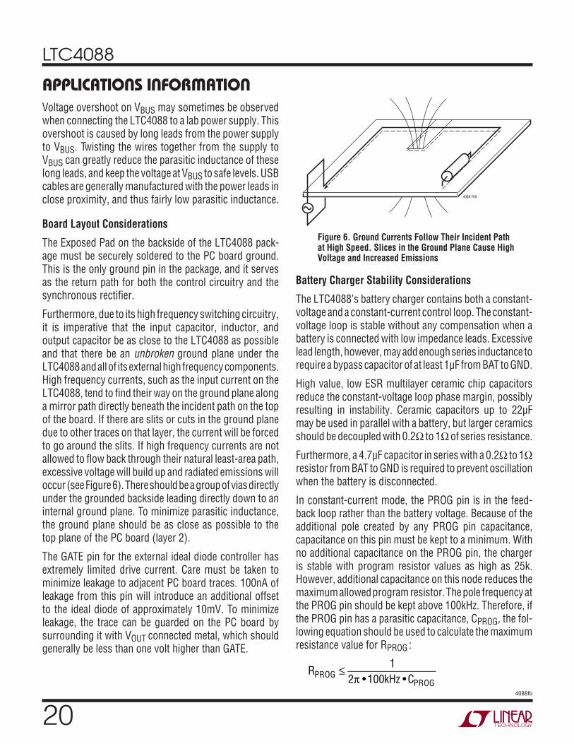
Furthermore, due to its high frequency switching circuitry, it is imperative that the input capacitor, inductor, and output capacitor be as close to the LTC4088 as possible and that there be an unbroken ground plane under the LTC4088 and all of its external high frequency components. High frequency currents, such as the input current on the LTC4088, tend to find their way on the ground plane along a mirror path directly beneath the incident path on the top of the board. If there are slits or cuts in the ground plane due to other traces on that layer, the current will be forced to go around the slits. If high frequency currents are not allowed to flow back through their natural least-area path, excessive voltage will build up and radiated emissions will occur (see Figure 6). There should be a group of vias directly under the grounded backside leading directly down to an internal ground plane. To minimize parasitic inductance, the ground plane should be as close as possible to the top plane of the PC board (layer 2).
The GATE pin for the external ideal diode controller has extremely limited drive current. Care must be taken to minimize leakage to adjacent PC board traces. 100nA of leakage from this pin will introduce an additional offset to the ideal diode of approximately 10mV. To minimize leakage, the trace can be guarded on the PC board by surrounding it with VOUT connected metal, which should generally be less than one volt higher than GATE.
Figure 6. Ground Currents Follow Their Incident Path at High Speed. Slices in the Ground Plane Cause High Voltage and Increased Emissions
4088 F06
Battery Charger Stability Considerations
The LTC4088’s battery charger contains both a constant-voltage and a constant-current control loop. The constant-voltage loop is stable without any compensation when a battery is connected with low impedance leads. Excessive lead length, however, may add enough series inductance to require a bypass capacitor of at least 1µF from BAT to GND.
High value, low ESR multilayer ceramic chip capacitors reduce the constant-voltage loop phase margin, possibly resulting in instability. Ceramic capacitors up to 22µF may be used in parallel with a battery, but larger ceramics should be decoupled with 0.2Ω to 1Ω of series resistance.
Furthermore, a 4.7µF capacitor in series with a 0.2Ω to 1Ω resistor from BAT to GND is required to prevent oscillation when the battery is disconnected.
In constant-current mode, the PROG pin is in the feed-back loop rather than the battery voltage. Because of the additional pole created by any PROG pin capacitance, capacitance on this pin must be kept to a minimum. With no additional capacitance on the PROG pin, the charger is stable with program resistor values as high as 25k. However, additional capacitance on this node reduces the maximum allowed program resistor. The pole frequency at the PROG pin should be kept above 100kHz. Therefore, if the PROG pin has a parasitic capacitance, CPROG, the fol-lowing equation should be used to calculate the maximum resistance value for R PROG :
RPROG ≤ 1
2π • 100kHz • CPROG
LTC4088
214088fb
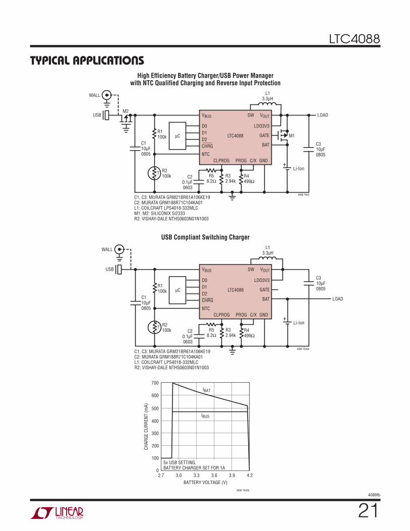
Typical applicaTionsHigh Efficiency Battery Charger/USB Power Manager
with NTC Qualified Charging and Reverse Input Protection
USB Compliant Switching Charger
+
VBUS
Li-Ion
VOUT
C110µF0805
WALL
USBM2
C20.1µF0603
C310µF0805
L13.3µH
M1
LOAD
R32.94k
R58.2Ω
R1100k
R2100k R4
499Ω
C1, C3: MURATA GRM21BR61A106KE19C2: MURATA GRM188R71C104KA01L1: COILCRAFT LPS4018-332MLCM1, M2: SILICONIX Si2333R2: VISHAY-DALE NTHS0603N01N1003
4088 TA02
µC
CLPROG PROG
LTC4088
C/X GND
SW
D0D1D2CHRG
NTC
LDO3V3
GATE
BAT
T
+
VBUS
Li-Ion
VOUT
C110µF0805
WALL
USB
C20.1µF0603
C310µF0805
L13.3µH
LOAD
R32.94k
R58.2Ω
R1100k
R2100k R4
499Ω
C1, C3: MURATA GRM21BR61A106KE19C2: MURATA GRM188R71C104KA01L1: COILCRAFT LPS4018-332MLCR2: VISHAY-DALE NTHS0603N01N1003
4088 TA03a
µC
CLPROG PROG
LTC4088
C/X GND
SW
D0D1D2CHRG
NTC
LDO3V3
GATE
BAT
T
BATTERY VOLTAGE (V)2.7
500
600IBAT
IBUS
700
3.9
4088 TA03b
400
300
3.0 3.3 3.6 4.2
200
100
0
CHAR
GE C
URRE
NT (m
A)
5x USB SETTING,BATTERY CHARGER SET FOR 1A

LTC4088
224088fb
package DescripTion
DE Package14-Lead Plastic DFN (4mm × 3mm)
(Reference LTC DWG # 05-08-1708 Rev B)
3.00 ±0.10(2 SIDES)
4.00 ±0.10(2 SIDES)
NOTE:1. DRAWING PROPOSED TO BE MADE VARIATION OF VERSION (WGED-3) IN JEDEC PACKAGE OUTLINE MO-2292. DRAWING NOT TO SCALE 3. ALL DIMENSIONS ARE IN MILLIMETERS4. DIMENSIONS OF EXPOSED PAD ON BOTTOM OF PACKAGE DO NOT INCLUDE MOLD FLASH. MOLD FLASH, IF PRESENT, SHALL NOT EXCEED 0.15mm ON ANY SIDE5. EXPOSED PAD SHALL BE SOLDER PLATED6. SHADED AREA IS ONLY A REFERENCE FOR PIN 1 LOCATION ON THE TOP AND BOTTOM OF PACKAGE
0.40 ±0.10
BOTTOM VIEW—EXPOSED PAD
1.70 ±0.10
0.75 ±0.05
R = 0.115TYP
R = 0.05TYP
3.00 REF
1.70 ±0.05
17
148
PIN 1TOP MARK
(SEE NOTE 6)
0.200 REF
0.00 – 0.05
(DE14) DFN 0806 REV B
PIN 1 NOTCHR = 0.20 OR0.35 × 45°CHAMFER
3.00 REF
RECOMMENDED SOLDER PAD PITCH AND DIMENSIONSAPPLY SOLDER MASK TO AREAS THAT ARE NOT SOLDERED
2.20 ±0.05
0.70 ±0.05
3.60 ±0.05
PACKAGEOUTLINE
0.25 ±0.05
0.25 ±0.050.50 BSC
3.30 ±0.05
3.30 ±0.10
0.50 BSC
DE Package14-Lead Plastic DFN (4mm × 3mm)
(Reference LTC DWG # 05-08-1708 Rev B)
Please refer to http://www.linear.com/designtools/packaging/ for the most recent package drawings.

LTC4088
234088fb
Information furnished by Linear Technology Corporation is believed to be accurate and reliable. However, no responsibility is assumed for its use. Linear Technology Corporation makes no representa-tion that the interconnection of its circuits as described herein will not infringe on existing patent rights.
revision hisToryREV DATE DESCRIPTION PAGE NUMBER
B 05/12 Clarified thermistor part number. 18, 21
(Revision history begins at Rev B)
LTC4088
244088fb
Linear Technology Corporation1630 McCarthy Blvd., Milpitas, CA 95035-7417 (408) 432-1900 FAX: (408) 434-0507 www.linear.com LINEAR TECHNOLOGY CORPORATION 2007
LT 0512 REV B • PRINTED IN USA
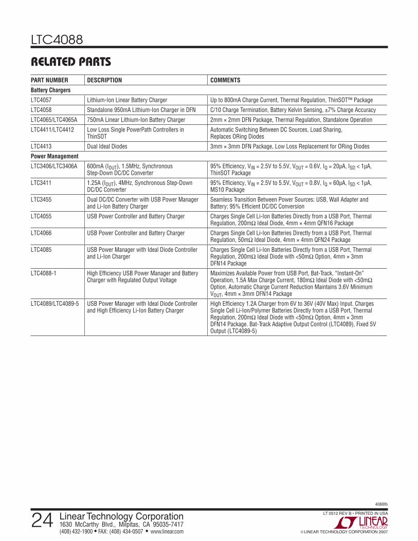
relaTeD parTsPART NUMBER DESCRIPTION COMMENTS
Battery Chargers
LTC4057 Lithium-Ion Linear Battery Charger Up to 800mA Charge Current, Thermal Regulation, ThinSOT™ Package
LTC4058 Standalone 950mA Lithium-Ion Charger in DFN C/10 Charge Termination, Battery Kelvin Sensing, ±7% Charge Accuracy
LTC4065/LTC4065A 750mA Linear Lithium-Ion Battery Charger 2mm × 2mm DFN Package, Thermal Regulation, Standalone Operation
LTC4411/LTC4412 Low Loss Single PowerPath Controllers in ThinSOT
Automatic Switching Between DC Sources, Load Sharing, Replaces ORing Diodes
LTC4413 Dual Ideal Diodes 3mm × 3mm DFN Package, Low Loss Replacement for ORing Diodes
Power Management
LTC3406/LTC3406A 600mA (IOUT), 1.5MHz, Synchronous Step-Down DC/DC Converter
95% Efficiency, VIN = 2.5V to 5.5V, VOUT = 0.6V, IQ = 20µA, ISD < 1µA, ThinSOT Package
LTC3411 1.25A (IOUT), 4MHz, Synchronous Step-Down DC/DC Converter
95% Efficiency, VIN = 2.5V to 5.5V, VOUT = 0.8V, IQ = 60µA, ISD < 1µA, MS10 Package
LTC3455 Dual DC/DC Converter with USB Power Manager and Li-Ion Battery Charger
Seamless Transition Between Power Sources: USB, Wall Adapter and Battery; 95% Efficient DC/DC Conversion
LTC4055 USB Power Controller and Battery Charger Charges Single Cell Li-Ion Batteries Directly from a USB Port, Thermal Regulation, 200mΩ Ideal Diode, 4mm × 4mm QFN16 Package
LTC4066 USB Power Controller and Battery Charger Charges Single Cell Li-Ion Batteries Directly from a USB Port, Thermal Regulation, 50mΩ Ideal Diode, 4mm × 4mm QFN24 Package
LTC4085 USB Power Manager with Ideal Diode Controller and Li-Ion Charger
Charges Single Cell Li-Ion Batteries Directly from a USB Port, Thermal Regulation, 200mΩ Ideal Diode with <50mΩ Option, 4mm × 3mm DFN14 Package
LTC4088-1 High Efficiency USB Power Manager and Battery Charger with Regulated Output Voltage
Maximizes Available Power from USB Port, Bat-Track, “Instant-On” Operation, 1.5A Max Charge Current, 180mΩ Ideal Diode with <50mΩ Option, Automatic Charge Current Reduction Maintains 3.6V Minimum VOUT, 4mm × 3mm DFN14 Package
LTC4089/LTC4089-5 USB Power Manager with Ideal Diode Controller and High Efficiency Li-Ion Battery Charger
High Efficiency 1.2A Charger from 6V to 36V (40V Max) Input. Charges Single Cell Li-Ion/Polymer Batteries Directly from a USB Port, Thermal Regulation, 200mΩ Ideal Diode with <50mΩ Option, 4mm × 3mm DFN14 Package. Bat-Track Adaptive Output Control (LTC4089), Fixed 5V Output (LTC4089-5)