low-power vlsipower vlsi - yonsei universitytera.yonsei.ac.kr/class/2011_1/lecture/topic_8_low-power...
TRANSCRIPT
Low Power VLSILow-Power VLSI
Seong-Ook Jungg g2011. 5. 6.
VLSI SYSTEM LAB, YONSEI UniversityS h l f El t i l & El t i E i iSchool of Electrical & Electronic Engineering

Contents1. Introduction2. Power classification3. Power – performance relationship4. Low power design
1. Architecture and algorithm level2. Block and logic level3. Circuit level4 Device level4. Device level
5. OMAP processor6 Summary6. Summary
2 YONSEI Univ. School of EEE
I t d tiI t d tiIntroductionIntroduction
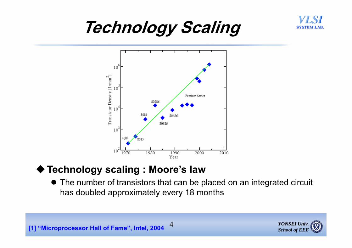
Technology Scaling
Technology scaling : Moore’s law Th b f t i t th t b l d i t t d i it The number of transistors that can be placed on an integrated circuit
has doubled approximately every 18 months
4 YONSEI Univ. School of EEE[1] “Microprocessor Hall of Fame”, Intel, 2004

Development TrendScaling (More Moore)
More devices are integrated in a More devices are integrated in a chip
New scaling road mapNot only ‘geometrical scaling’ for
2D device, but also ‘equivalent scaling’ for 3D device
Beyond bulk CMOSFinFET, SOI…
F ti l di ifi tiFunctional diversification (More than Moore) Several functions are merged in Several functions are merged in
a chip
5 YONSEI Univ. School of EEE[2] ITRS (International Technology Roadmap for Semiconductors) 2009

SoC Performance
SoC performance : exponentially increase!! Thanks to both device technology and design methodology
6 YONSEI Univ. School of EEE[2] ITRS 2009

SoC Power Consumption Problem
SoC power consumption : ‘also’ severely increase After 15 years, x10 power is required…
7 YONSEI Univ. School of EEE[2] ITRS 2009

SoC Power Density Problem
Power density : exponentially increase!! Power consumption per die area (W/cm2) We would soon reach power densities of nuclear power plants or
rocket nozzles in a few years!!
8 YONSEI Univ. School of EEE
y
[1] “Microprocessor Hall of Fame”, Intel, 2004

Process Variation ProblemProcess variation : Result of scaling
Global variation and local variationGlobal variation
Comes from fabrication, lot, wafer processes, , p Different process corner (NMOS-PMOS : SS/SF/TT/FS/FF)
Local variation Truly random variation between device with identical layout Truly random variation between device with identical layout
9 YONSEI Univ. School of EEE
[4] http://cnx.org[3] Synopsis, 2005

Process Variation Problem
Performance variation due to process variation Frequency difference ≈ 30% Leakage current difference ≈ x20⇒ Process variation should be considered in SoC design
10 YONSEI Univ. School of EEE[5] A. Devgan, Berkeley
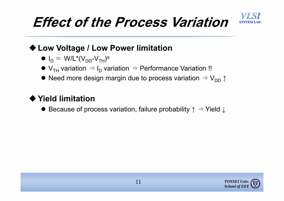
Effect of the Process VariationLow Voltage / Low Power limitation
ID∝W/L*(VDD-VTH)α
VTH variation ⇒ ID variation ⇒ Performance Variation !! Need more design margin due to process variation⇒ V ↑ Need more design margin due to process variation ⇒ VDD ↑
Yield limitationYield limitation Because of process variation, failure probability ↑ ⇒ Yield ↓
11 YONSEI Univ. School of EEE

저전력 SoC
Low power VLSI design !!! Low process variation (high yield) design Low process variation (high yield) design
12 YONSEI Univ. School of EEE[1] ITRS Roadmap 2009

P Cl ifi tiP Cl ifi tiPower ClassificationPower Classification

Power ClassificationPower consumption of CMOS circuits
Ptotal = Pdynamic + Pstatic
Pdynamic = Psw + Psc
14 YONSEI Univ. School of EEE
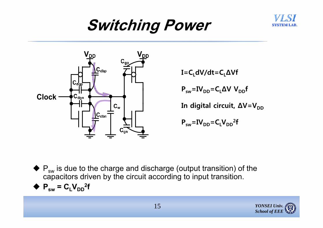
Switching Power
I=CLdV/dt=CLΔVf
P IV C ΔV V fPsw=IVDD=CLΔV VDDf
In digital circuit, ΔV=VDD
Psw=IVDD=CLVDD2f
P i d t th h d di h ( t t t iti ) f th Psw is due to the charge and discharge (output transition) of the capacitors driven by the circuit according to input transition.
Psw = CLVDD2f
15 YONSEI Univ. School of EEE

Short Circuit Power
P i d b th i lt d t f PMOS d NMOS Psc is caused by the simultaneous conductance of PMOS and NMOS during input and output transitions.
Psc = (β/12)(VDD-2VTH)3 (t3-t1)
16 YONSEI Univ. School of EEE

Static Power : Psub, Pgate & Pjunc
Psub Sub-VTH leakage : |VGS|<|VTH| Psub∝ Exp[(VGS-VTH)/mvT ] VDD
Pgate Ideal MOSFET : Igate = 0
I h t h l MOSFET I In short channel MOSFET, Igateexists because of thin TOX
Pgate∝WL (VGS/TOX)2 VDDgate ( GS OX) DD
Pjunc Reverse PN junction leakageReverse PN junction leakage Pjunc∝ Exp[VD/vT -1] VDD
17 YONSEI Univ. School of EEE[6] K.M.Cao, “BSIM4 Gate Leakage Model Including Source-Drain Partition”, IEDM, 2000

PowerPower –– PerformancePerformancePower Power Performance Performance RelationshipRelationshippp

VDD ReductionPower consumption equation
Psw = CLVDD2f
Psc = (β/12) (VDD-2VTH)3 (t3-t1) P ∝ Exp[(V V )/mv ] V Psub∝ Exp[(VGS-VTH)/mvT ] VDD
Pgate∝WL (VGS/TOX)2 VDD
Pjunc∝ Exp[VD/vT -1] VDDjunc p[ D T ] DD
Case.1 : VDD ↓DD ↓ All power consumption ↓ However…
Delay ∝ CLVDD/ID∝ CLVDD/(VDD-VTH)α
If VDD ↓, Delay ↑ Performance loss
19 YONSEI Univ. School of EEE
e o a ce oss

VDD Scaling LimitationLow VDD limitation with process variation
VDD.min = VT0+Kσ(VT)σ(VT) : 1-sigma of VT variation
∝ToxNA0.25(LW)-0.5
ox A ( )
Significant increment of σ(VT) withtechnology scaling (LW↓↓)
VDD scaling meets the limitation!!
Process variation tolerant circuitdesign technique is required!!g q q
20 YONSEI Univ. School of EEE[7] K.Itoh, “Adaptive Circuits for the 0.5-V Nanoscale CMOS Era”, ISSCC, 2009

High VTH
Power consumption equation Psw = CLVDD
2f Psc = (β/12) (VDD-2VTH)3 (t3-t1) P ∝ Exp[(V V )/mv ] V Psub∝ Exp[(VGS-VTH)/mvT ] VDD
Pgate∝WL (VGS/TOX)2 VDD
Pjunc∝ Exp[VD/vT -1] VDDjunc p[ D T ] DD
Case.2 : VTH ↑TH ↑ Psc ↓ and especially, Psub ↓ However…
Delay ∝ CLVDD/ID∝ CLVDD/(VDD-VTH)α
If VTH ↑, Delay ↑Performance loss
21 YONSEI Univ. School of EEE
e o a ce oss
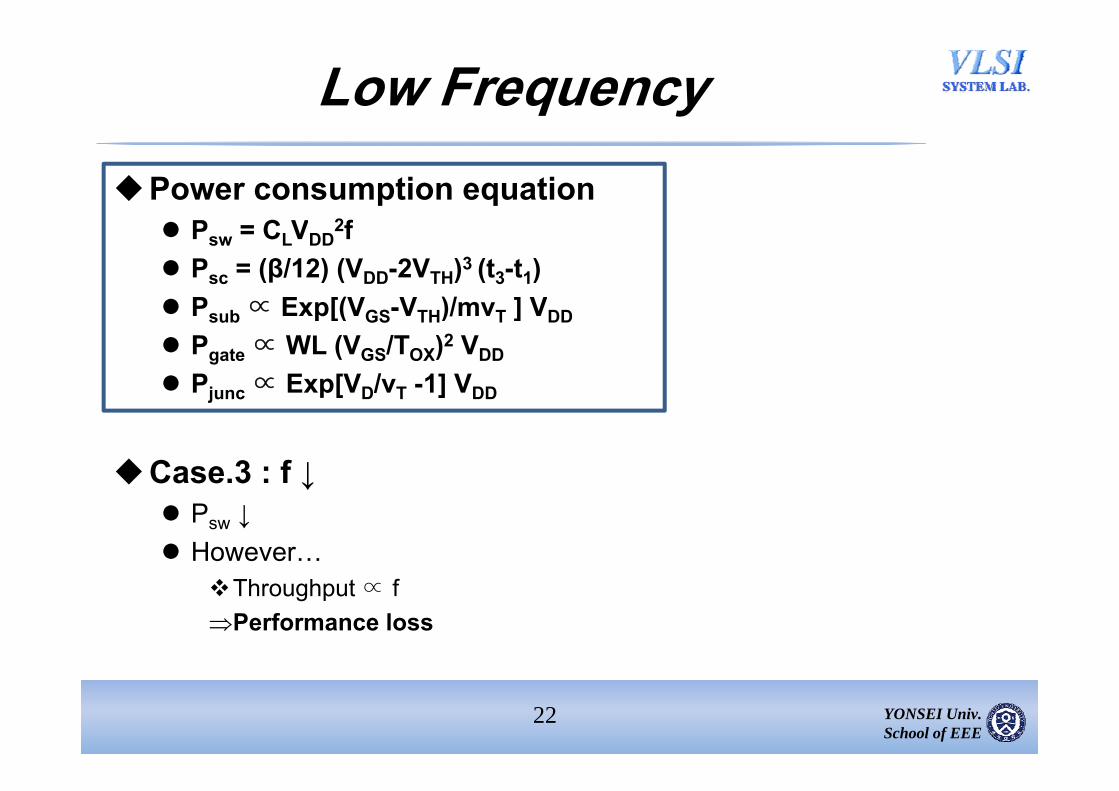
Low FrequencyPower consumption equation
Psw = CLVDD2f
Psc = (β/12) (VDD-2VTH)3 (t3-t1) P ∝ Exp[(V V )/mv ] V Psub∝ Exp[(VGS-VTH)/mvT ] VDD
Pgate∝WL (VGS/TOX)2 VDD
Pjunc∝ Exp[VD/vT -1] VDDjunc p[ D T ] DD
Case.3 : f ↓↓ Psw ↓ However…
Throughput ∝ fPerformance loss
22 YONSEI Univ. School of EEE
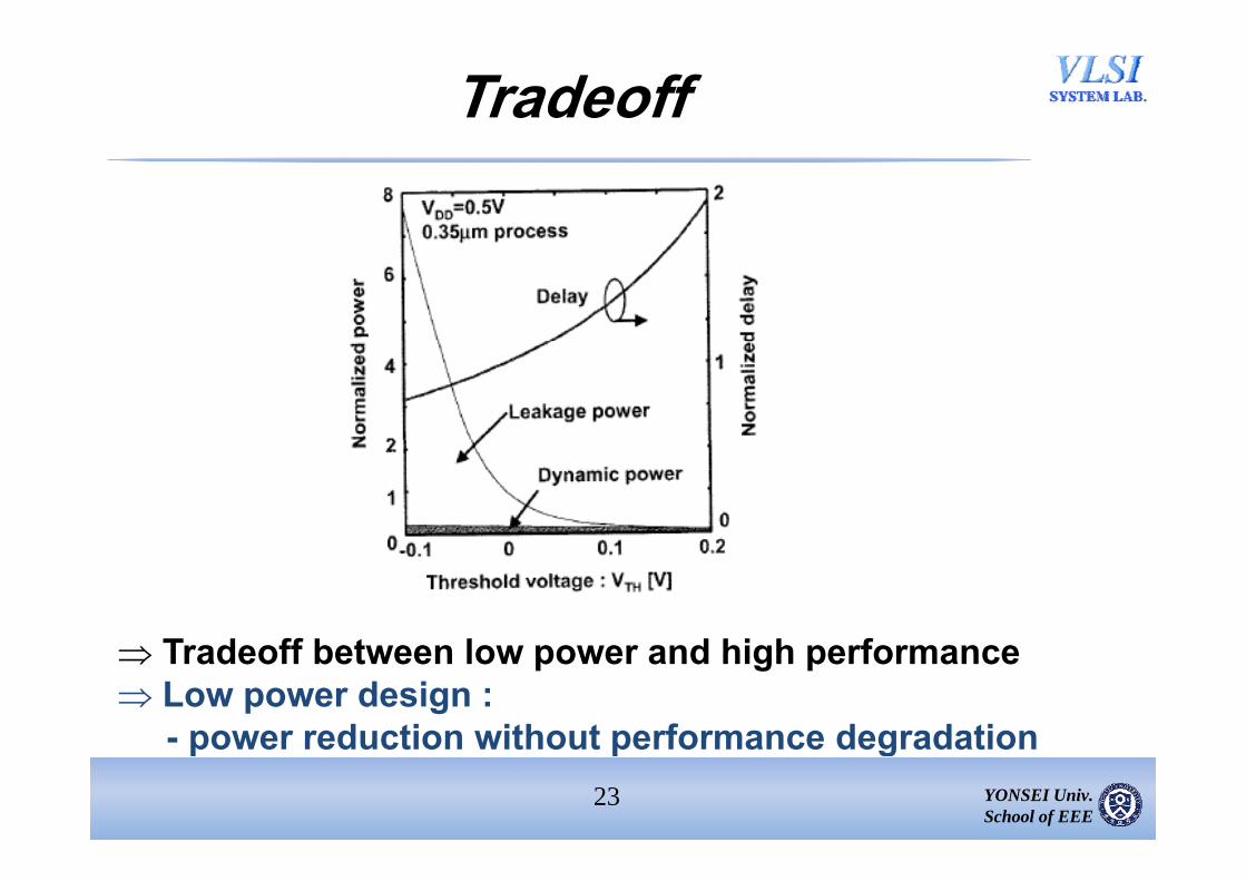
Tradeoff
T d ff b t l d hi h f Tradeoff between low power and high performance Low power design :
- power reduction without performance degradation23 YONSEI Univ.
School of EEE
- power reduction without performance degradation

L d iL d iLow power designLow power design

Low Power Design MethodologyTo make low power SoC…
Architecture and algorithm levels Architecture and algorithm levelsParallelism, Pipeline …
Block and logic levelsVDD / Frequency scheduling by monitoring workload (AVFS)Temperature management to reduce leakage current
Circuit level Circuit levelCircuit type (Dynamic, static, …)Circuit technique (Dual VDD, Dual VTH, MTCMOS, …
Device levelControl the process parameter
Halo doping retrograde well Halo doping, retrograde well…Low leakage new device
SOI, FinFET …
25 YONSEI Univ. School of EEE
A hit t d Al ith L lA hit t d Al ith L lArchitecture and Algorithm LevelsArchitecture and Algorithm Levels
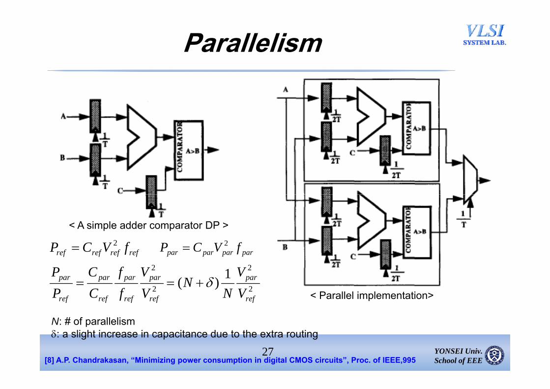
Parallelism
< A simple adder comparator DP >
refrefrefref fVCP 2 parparparpar fVCP 222 1)( parparparparpar V
NVfCP
22 )(refrefrefrefref VN
NVfCP
N: # of parallelism
< Parallel implementation>
27 YONSEI Univ. School of EEE
: a slight increase in capacitance due to the extra routing
[8] A.P. Chandrakasan, “Minimizing power consumption in digital CMOS circuits”, Proc. of IEEE,995

Pipeline
refrefrefref fVCP 2
< A simple adder comparator DP > < Pipeline implementation>
pipepipepipepipe fVCP 2refrefrefref f pipepipepipepipe
2
2
2
2
)1(ref
pipe
ref
pipe
ref
pipe
ref
pipe
ref
pipe
VV
VV
ff
CC
PP
refrefrefrefref VVfCP
N: # of pipeline stage: a slight increase in capacitance due to the extra latch
28 YONSEI Univ. School of EEE
: a slight increase in capacitance due to the extra latch
[8] A.P. Chandrakasan, “Minimizing power consumption in digital CMOS circuits”, Proc. of IEEE,995

Ci itCi it L lL lCircuit Circuit LevelLevel

Circuit Level Low Power Techniques
Low power techniques Multiple channel length Stacked transistor Dual V Dual VDD
Dual VTH
MTCMOS (Multi Threshold voltage CMOS)( g ) DVS (Dynamic Voltage Scaling) : open-loop / closed loop
30 YONSEI Univ. School of EEE

Critical Path
Critical Path : The worst case delay path Determines SoC’s maximum performance # of critical path << # of non-critical path Fast non critical path is just wasteful Fast non-critical path is just wasteful…
By increasing non-critical path’s delay, we may achieve power reduction because of tradeoff relation between power & performance
31 YONSEI Univ. School of EEE

Multiple Channel LengthThreshold voltage roll-off
Longer L Higher VtLow leakage with low performanceg pUsed in non-critical path
32 YONSEI Univ. School of EEE
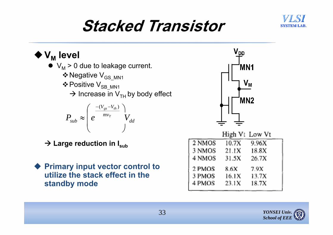
Stacked TransistorVM level
V > 0 d t l k t VM > 0 due to leakage current.Negative VGS_MN1Positive VSB_MN1 Increase in VTH by body effect
mvVV
VeP T
thgs
)(
Large reduction in I b
ddsub VeP
Large reduction in Isub
Primary input vector control to utilize the stack effect in the standby mode
33 YONSEI Univ. School of EEE

Dual VDD
Basic idea VDDL
Logic gates off the critical path VDDH VDDH
Logic gate on the critical path Reduce power without
degrading the performance
Shaded : VDDLNon-shaded: VDDH
34 YONSEI Univ. School of EEE

Dual VDD : Design Issue & Target
Issue St ti t fl t V
VSG>0
Static Static current flow at a VDDH
gate if it is directly drive by a VDDL gate
Current
Level converter is neededOverhead of area and power
Design target For a give circuit choose gates for V application to minimize For a give circuit, choose gates for VDDL application to minimize
power consumption while maintaining performance with consider level converter.
35 YONSEI Univ. School of EEE

Dual VTH Voltages
HVt HVt Assigned to transistors in noncritical path. Leakage saving in both standby and active modes
LVt Assigned to transistors in critical path Maintained performance
36 YONSEI Univ. School of EEE
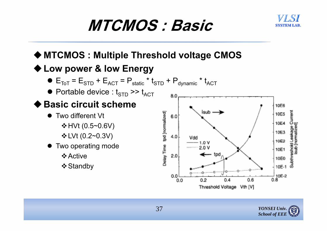
MTCMOS : BasicMTCMOS : Multiple Threshold voltage CMOSLow power & low Energy
EToT = ESTD + EACT = Pstatic * tSTD + Pdynamic * tACT
P t bl d i t t Portable device : tSTD >> tACT
Basic circuit scheme Two different Vt Two different Vt
HVt (0.5~0.6V) LVt (0.2~0.3V)
Two operating modeActive StandbyStandby
37 YONSEI Univ. School of EEE

MTCMOS : SchemeActive mode
SL=1 / SL=0 VDDVVDD / VGNDVVGND
LVt operating frequencyp g q y
Standby mode y SL=0 / SL=1 VDDV & VGNDV = floating HVt l k HVt leakage
38 YONSEI Univ. School of EEE

MTCMOS : Constraint
Performance constraint according tog Normalized foot/head switch size : WH/WL
Normalized cap on VDDV/VGNDV : CV/CO
Area penalty Relatively small because Head/Footswitches are shared by all logic gates
on a chip (global foot switch)
39 YONSEI Univ. School of EEE
p (g )
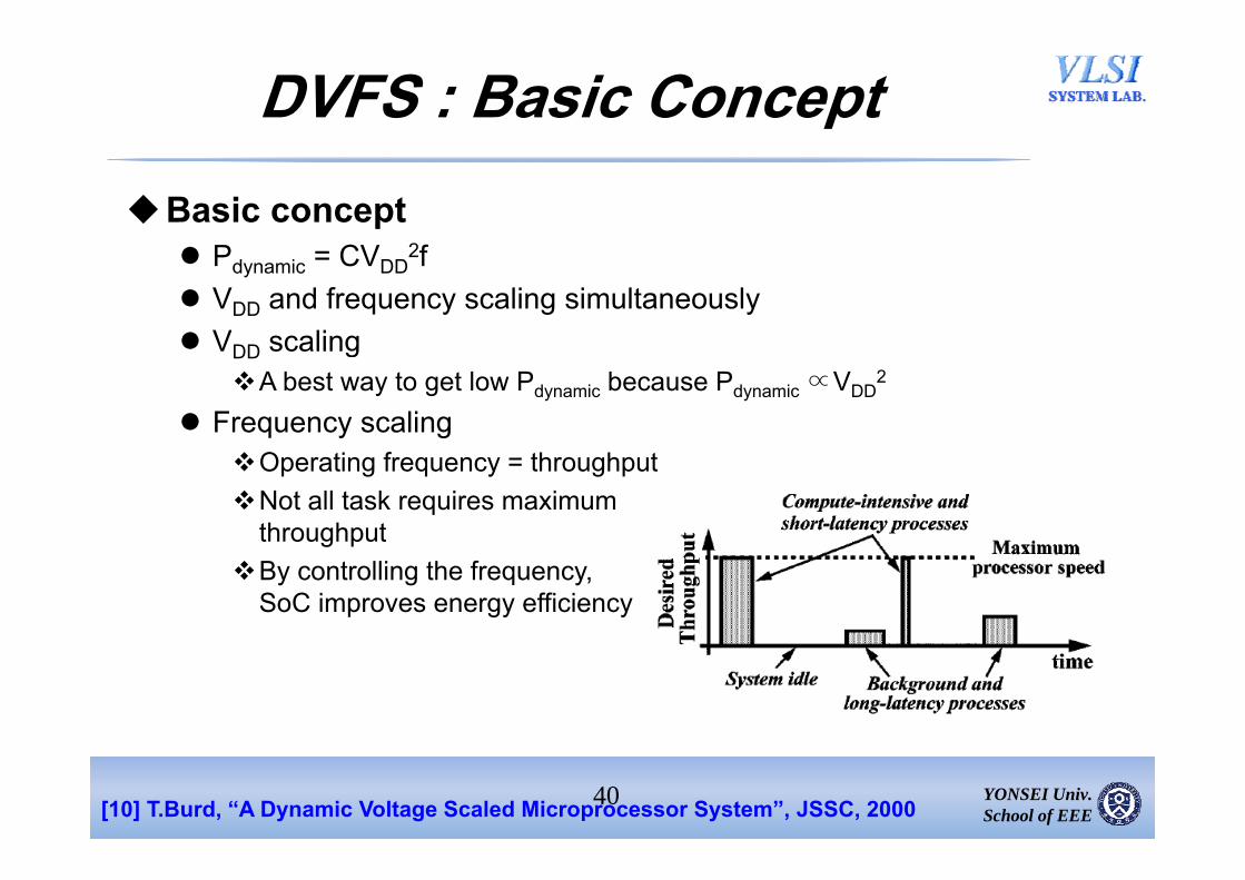
DVFS : Basic ConceptBasic concept
Pdynamic = CVDD2f
VDD and frequency scaling simultaneously V scaling VDD scaling
A best way to get low Pdynamic because Pdynamic∝VDD2
Frequency scalingOperating frequency = throughputNot all task requires maximum
throughputthroughputBy controlling the frequency,
SoC improves energy efficiency
40 YONSEI Univ. School of EEE[10] T.Burd, “A Dynamic Voltage Scaled Microprocessor System”, JSSC, 2000
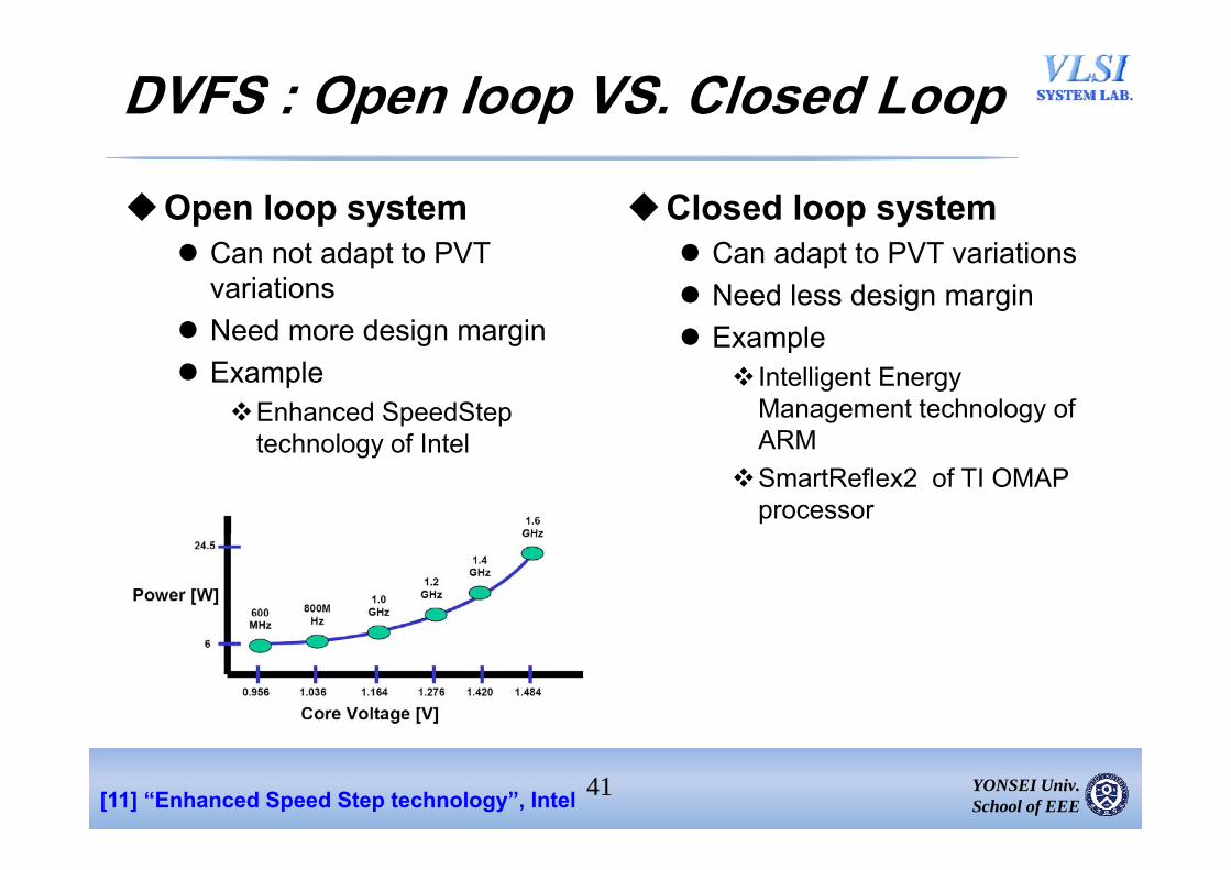
DVFS : Open loop VS. Closed Loop
Open loop system Closed loop system Can not adapt to PVT
variations Need more design margin
Can adapt to PVT variations Need less design margin Example Need more design margin
ExampleEnhanced SpeedStep
t h l f I t l
Example Intelligent Energy
Management technology of ARMtechnology of Intel ARM
SmartReflex2 of TI OMAP processor
41 YONSEI Univ. School of EEE[11] “Enhanced Speed Step technology”, Intel

DVFS (SONY, PDA)Block Diagram
Closed loop system
42 YONSEI Univ. School of EEE
p y
[12] M.Nakai, “Dynamic Voltage and Frequency Management for a Low-Power Embedded Microprocessor”, JSSC, 2005
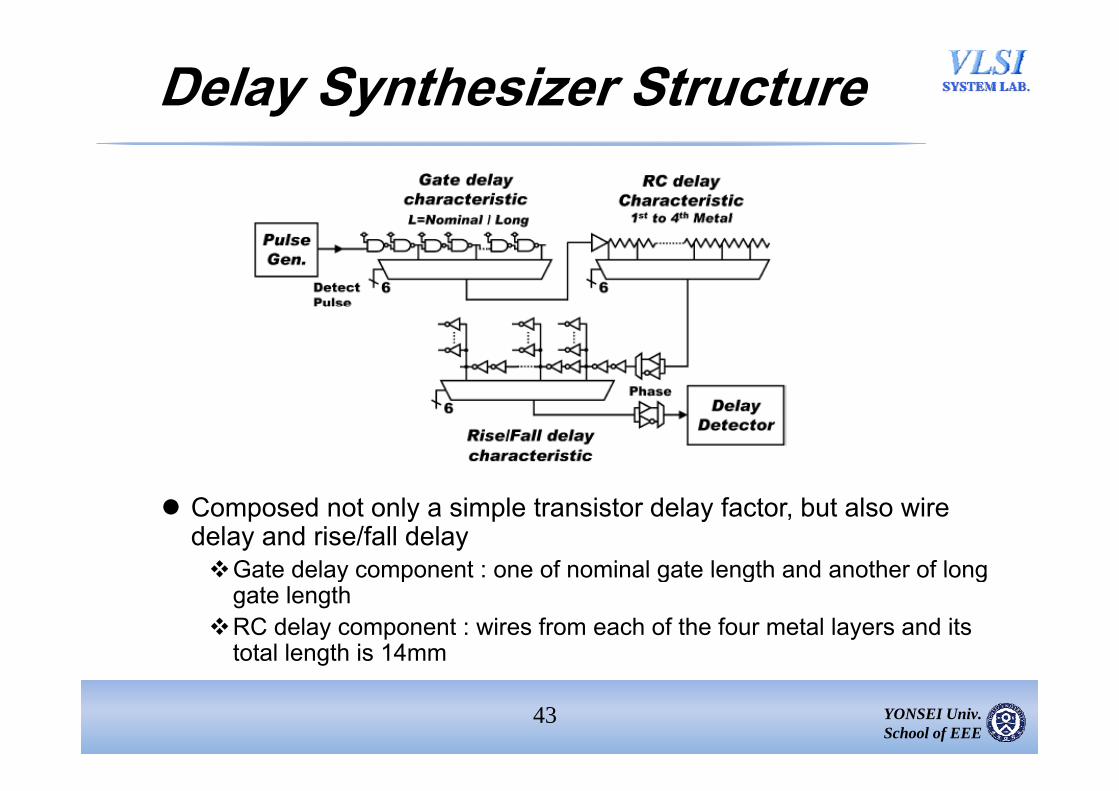
Delay Synthesizer Structure
Composed not only a simple transistor delay factor, but also wire delay and rise/fall delayGate delay component : one of nominal gate length and another of longGate delay component : one of nominal gate length and another of long
gate lengthRC delay component : wires from each of the four metal layers and its
total length is 14mm
43 YONSEI Univ. School of EEE
g

Delay Synthesizer Effect
44 YONSEI Univ. School of EEE
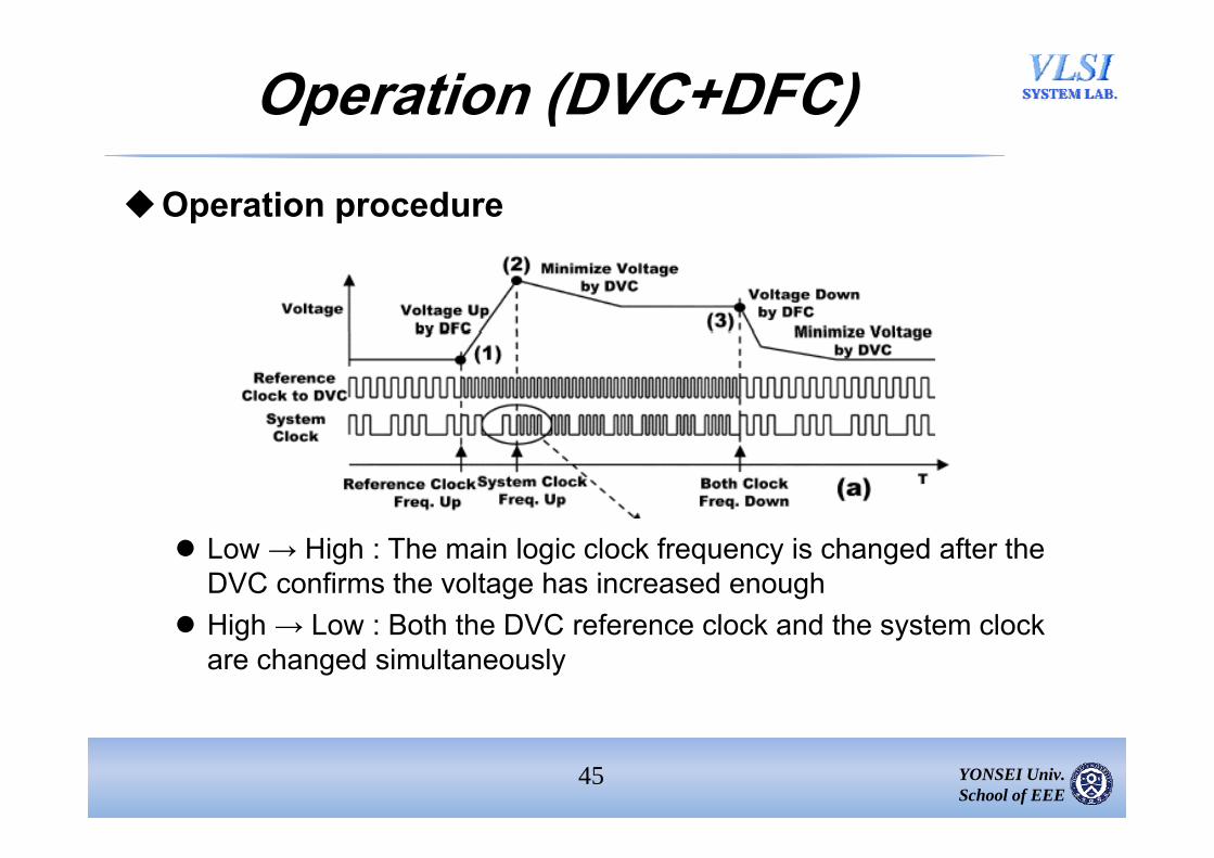
Operation (DVC+DFC)Operation procedure
Low → High : The main logic clock frequency is changed after the DVC confirms the voltage has increased enough
High → Low : Both the DVC reference clock and the system clock High → Low : Both the DVC reference clock and the system clock are changed simultaneously
45 YONSEI Univ. School of EEE

D i L lD i L lDevice LevelDevice Level

Device Level Low Power Technique
FinFET FinFET : Vertical structure
Planar MOSFET width = FinFET heightg
σ(VT) ∝ToxNA0.25(LW)-0.5
As scaling goes on, variation of planar MOSFET get worse VDD scaling is impossible
However, FinFET’s σ(VT) doesn’t degraded FinFET width doesn’t occupy the active area As scaling goes on, L*W of FinFET can be maintained VDD scaling is possible ⇒ low power !!
47 YONSEI Univ. School of EEE[7] K.Itoh, “Adaptive Circuits for the 0.5-V Nanoscale CMOS Era”, ISSCC, 2009

OMAP POMAP POMAP ProcessorOMAP Processor

OMAP ProcessorOMAP Processor
Dual core platform Multimedia hardware accelerators for video and graphics Frame buffers Frame buffers Various dedicated and general purpose interfaces
Power saving modePower saving mode Idle (Clock stopped) Retention for low leakage Fast re-start and power-off mode Power gating technique
49 YONSEI Univ. School of EEEISSCC05, 138-139
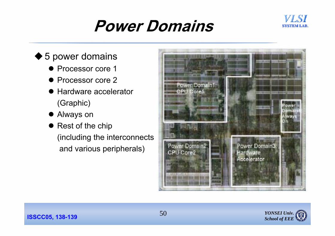
Power Domains5 power domains
Processor core 1 Processor core 2 Hardware accelerator Hardware accelerator
(Graphic) Always ony Rest of the chip
(including the interconnectsand various peripherals)
50 YONSEI Univ. School of EEEISSCC05, 138-139

Power Gating Power gating
Global mesh built with the highest metal layer distributes power and Global mesh built with the highest metal layer distributes power and ground across the chip
Local mesh is broken to reflect the power domain partitioning P it h k ti b t l b l h d l l h Power switch makes connection between global mesh and local mesh
according to operating modes and switch control If power domain is on, its power switches connect its local plane to the global
plane i e the constant power supplyplane., i.e., the constant power supplyOtherwise that plane drifts to a potential near ground
Power switch Embedded in power domains
by placing power switches at a regular pitch in a staggered manner by placing power switches around hard Ips
Header switch 90um PMOS with 200uA current driving capability at worst caseMultiple fingers and redundant vias
51 YONSEI Univ. School of EEEISSCC05, 138-139
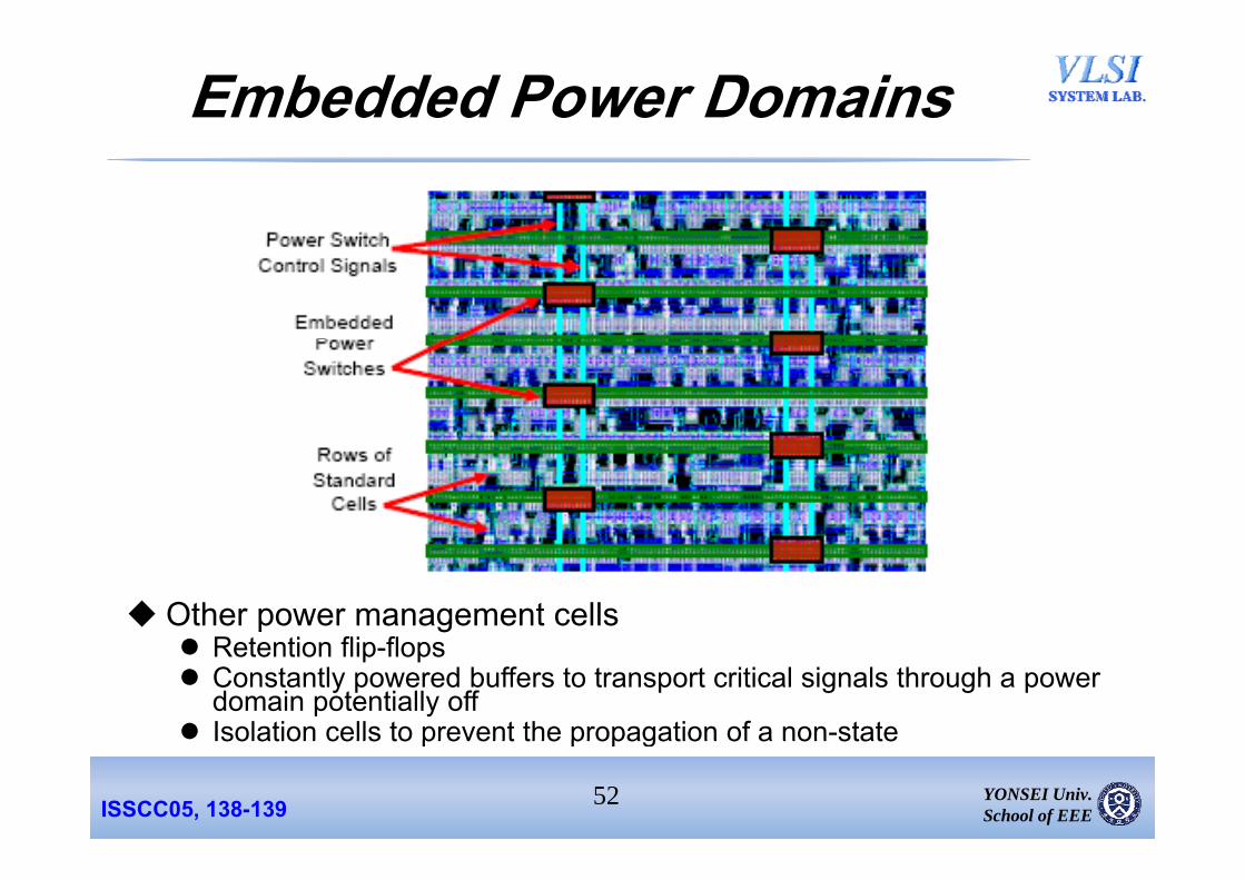
Embedded Power Domains
Other power management cells R t ti fli fl Retention flip-flops Constantly powered buffers to transport critical signals through a power
domain potentially off Isolation cells to prevent the propagation of a non-state
52 YONSEI Univ. School of EEE
Isolation cells to prevent the propagation of a non state
ISSCC05, 138-139

Power Switching Control
Current surges and dynamic IR drop Two-pass turn-on mechanism
Weak PMOS to sinks low current for power restore: Turn-on firstStrong PMOS to deliver current for normal operation: Turn-on next
53 YONSEI Univ. School of EEE
g p
ISSCC05, 138-139
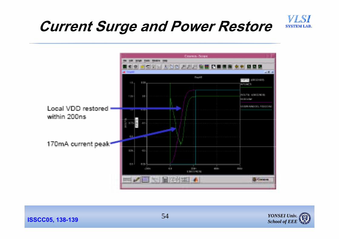
Current Surge and Power Restore
54 YONSEI Univ. School of EEEISSCC05, 138-139

Leakage Current Reduction In off mode
Leakage current comes from power switches and power management cells
4 power switches per Kgate 4 power switches per Kgate~40X leakage reduction
55 YONSEI Univ. School of EEEISSCC05, 138-139
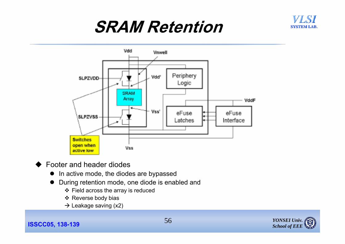
SRAM Retention
Footer and header diodes In active mode, the diodes are bypassed During retention mode, one diode is enabled and
Field across the array is reduced Reverse body bias Leakage saving (x2)
56 YONSEI Univ. School of EEE
Leakage saving (x2)
ISSCC05, 138-139

Dual Gate Length
Dual gate length Standby mode: 30% leakage reductionStandby mode: 30% leakage reduction Active mode: active leakage current saving: very useful if many blocks are idle in
active mode Vdd scaling during the slow active mode
300 V li 2X l k d ti
57 YONSEI Univ. School of EEE
300mV scaling: 2X leakage reduction
ISSCC05, 138-139
SSSummarySummary

Summary Green SoC design
Low power & process variation tolerant SoC design Low power & process variation tolerant SoC design P = Psw + Psc + Psub + Pgate + Pjunc
Pdynamic Pstaticdynamic static Power and performance : Trade-off Low power design
Architecture and algorithm level : parallelism, pipe lineArchitecture and algorithm level : parallelism, pipe line Block and logic level : workload monitoring, VDD/frequency scheduling Circuit level
Long channel : Reduce Ileak by using VTH roll off (VTH↑) St k d MOSFET R d I b i b d ff t (V ) & ti V Stacked MOSFET : Reduce Ileak by using body effect (VTH↑) & negative VGS Dual VDD : Use low VDD at non-critical path Dual VTH : Use low VTH at non-critical path MTCMOS: Use high VTH sleep TR (low leakage in stand-by mode) & low VTH logic (high TH TH
performance in active mode) DVFS : Reduce dynamic power by controlling both VDD & frequency
Device level : FinFET
59 YONSEI Univ. School of EEE