low-power cmos receivers for short reach …tcc/sharif-bakhtiar_invited_cicc17.pdflow-power cmos...
TRANSCRIPT

Low-Power CMOS Receivers For Short ReachOptical Communication
Alireza Sharif-Bakhtiar1, Michael G. Lee2, Anthony Chan Carusone11Department of Electrical and Computer Engineering, University of Toronto, e-mail: [email protected]
2Fujitsu Labs of America
Abstract—Emerging applications for short-reach optical com-munication require low-power receiver circuits in nanoscaleCMOS technologies. An analysis of optical receivers with broad-band input transimpedance reveals that their power consumptionincreases rapidly as bit-rate increases. This has motivated workon bandwidth-limited optical receiver front-ends. For example,receivers employing decision feedback equalization (DFE) andcorrelated-double sampling (CDS) are analyzed, showing thatthey significantly relax the bandwidth requirements of the analogfront-ends, permitting their low-power implementation in CMOS.Finally the design of an optical receiver utilizing an integrate-and-dump (ID) front-end is described. The receiver is implementedin 28nm CMOS and achieves -8.3dBm sensitivity at 20Gbpsconsuming 0.7pJ/b.
I. INTRODUCTION
The rapid increase in the speed demanded of wirelinelinks within data centers and high performance computing hasincreased the size and weight of copper cabling and the powerconsumption of the associated transceiver circuits makingthem increasingly prohibitive. Hence, optical links utilizingmulti-mode fiber (MMF) are increasingly seen as preferablefor link reaches up to 300m, particularly for links of 3-50mwhere the optical dispersion of the fiber is negligible [1]. Oversuch short distances, large numbers of transceiers must operatein parallel with high port density. This makes it important toreduce the power consumption per link. Ultimately it is desir-able to integrate the optical transceiver circuitry on the samedie as large CMOS ASICs that direct and process data traffic.Doing so will eliminate the need for very-short reach (VSR)wireline transceivers communicating over PCB traces betweenthe ASIC and off-chip optical transceiver circuits. Doing sorequires the optical receiver front-end to be implemened innanoscale CMOS technologies.
Implementation of the optical receiver front-end innanoscale CMOS presents both opportunities and challenges.Nanoscale CMOS is notorious for its relatively low intrinsictransistor gain, making it difficult to realize a high-gain lownoise front-end. However, CMOS affords a designer very high-speed switches and low-power high-speed latches and digitallogic. This paper will illustrate design techniques developedfor optical receivers that exploit the benefits of nanoscaleCMOS to obviate its challenges.
This paper is organized as follows: Section II analyzesoptical receivers with conventional wideband transimpedancefront-ends which typically have a bandwidth of 70% the linksymbol rate or more. It explains how such front-ends become
PD TIA+Amp CDR + Digital
PCB
Fiber
(a)
PD Optical Rx + Digital
PCB
Fiber
(b)
Fig. 1: (a) Conventional system where optical receiver anddigital circuits are on separate chips connected by PCB traces.(b) Integrating the optical receiver with the digital chip.
increasingly less power efficient as the data rate increases.This has motivated the development of optical receiver front-ends with bandwidths far below the symbol rate. SectionIII explains the benefits and the trade-offs in designing areceiver that combines a limited bandwidth front-end witha decision feedback equalizer (DFE). It will be seen thatreducing the front-end bandwidth and removing the resultingintersymbol interference (ISI) using a DFE not only results inhigher vertical eye-opening for a given power consumption,it also improves the receiver sensitivity. Section IV explainsthe operation of correlated double sampling (CDS) receivers.Due to their feed forward structure, these receivers do notsuffer from a critical timing path in a feedback loop, which canlimit the maximum operating speed of DFE-based receivers.However, their sensitivity is limited below what is achievablewith DFE-based receivers. Section V explains the operationand design of an integrate-and-dump (ID) receiver. It will beseen that an ID stage can provide a large gain and also filterout the high frequency noise of the stages preceding it. UnlikeDFE-based receivers, ID receivers lack a feedback loop andhence can be operated at higher speed. A prototype is designedand fabricated in 28nm CMOS. The receiver reaches -8.3dBmsensitivity at 20Gbps with 0.7pJ/b power efficiency.
II. WIDEBAND FRONT-ENDS
The discrete reverse-biased photodiodes typical for short-reach optical communication can be modeled with a currentsource in parallel with a parasitic capacitance CPD. Thephotocurrent (IPD) is linearly proportional to the powerof incoming light with the conversion gain referred to as
978-1-5090-5191-5/17/$31.00@2017 IEEE
ACIN
RINIPD CPD
PD
VA
VIN
(a)
TIA N-stagePost Amplifier
ASATIA
APA=NAS
(b)
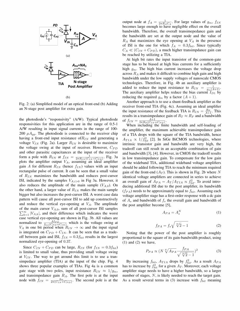
Fig. 2: (a) Simplified model of an optical front-end (b) Addingan N-stage post amplifier for extra gain.
the photodiode’s “responsivity” (A/W). Typical photodioderesponsivities for this application are in the range of 0.5-1A/W resulting in input signal currents in the range of 100-200 µApp. The photodiode is connected to the receiver chiphaving a front-end input resistance ofRIN and generating avoltage VIN (Fig. 2a). Larger RIN is desirable to maximizethe voltage swing at the input of receiver. However, CPDand other parasitic capacitances at the input of the receiverform a pole with RIN at fIN = 1
2πRIN (CIN+CPD) . Fig. 3aplots the amplifier output VA, assuming an ideal amplifiergain A for different RIN (hence fIN ) values with an inputrectangular pulse of current. It can be seen that a small valueof RIN maximizes the bandwidth and reduces post-cursorISI, indicated by the samples VA,i>0 in Fig 3a. However, italso reduces the amplitude of the main sample (VA,0). Onthe other hand, a larger value of RIN makes the main samplebigger but also increases the post-cursor ISI. A worst case datapattern will cause all post-cursor ISI to add up constructivelyand reduce the vertical eye-opening at VA. The amplitudeof the main cursor VA,0, sum of all post-cursor ISI samples∑∞k=1 |VA,k|, and their difference which indicates the worst
case vertical eye-opening are shown in Fig. 3b. All values arenormalized to AIPD
fbit(CPD+CIN ) which is the voltage swing atVA in one bit period when RIN → ∞ and the input signalis integrated on CPD + CIN . It can be seen that as a trade-off between gain and ISI, fIN = 0.3fbit results in the largestnormalized eye-opening of 0.37.
Since CIN + CPD can be large, RIN (for fIN = 0.3fbit)is limited to small value, thus providing small voltage swingat VIN . The way to get around this limit is to use a tran-simpedace amplifier (TIA) at the input of the chip. Fig. 4shows three popular examples of TIAs. Fig 4a is a commongate stage with two poles, input resistance RIN ≈ 1/gm,and transimpedance gain RA. The first pole is at the inputnode with fIN = gm
2π(CIN+CPD) . The second pole is at the
output node at fA = 12πRACA
. For large values of gm, fINbecomes large enough to have negligible effect on the overallbandwidth. Therefore, the overall transimepedance gain andthe bandwidth are set at the output node and the value ofRA that maximizes the eye opening at VA in the presenceof ISI is the one for which fA = 0.3fbit. Since typicallyCA (CIN +CPD), a much higher transimpdance gain canbe reached by utilizing a TIA.
At high bit rates the input transistor of the common-gatestage has to be biased at high bias currents for a sufficientlyhigh gm. The high bias current increases the voltage dropacross RA and makes it difficult to combine high gain and highbandwidth under the low supply voltages of nanoscale CMOStechnologies. Therefore, in Fig. 4b an auxiliary amplifier isadded to reduce the input resistance to RIN = 1
gm(A+1) .The auxiliary amplifier helps reduce the bias current ID1 byreducing the required gm by a factor (A+ 1).
Another approach is to use a shunt-feedback amplifier as thereceiver front-end TIA (Fig. 4c). Assuming an ideal amplifierthe input resistance of the feedback TIA is RIN = RF
A+1 . Thisresults in a transimpedance gain of RT ≈ RF and a bandwidthof fIN = A+1
2πRF (CIN+CPD) .When including the finite bandwidth and self-loading of
the amplifier, the maximum achievable transimpedance gainof a TIA drops with the square of the TIA bandwidth, henceATIA ∝ 1/f2bit [2]. In SiGe BiCMOS technologies, whereintrinsic transistor gain and bandwidth are very high, thetradeoff can still result in an acceptable combination of gainand bandwidth [3], [4]. However, in CMOS the tradeoff resultsin low transimpedance gain. To compensate for the low gainof the wideband TIA, additional wideband voltage amplifiersshould be added following TIA to reach the minimum requiredgain of the front-end (AT ). This is shown in Fig. 2b where Nidentical voltage amplifiers are connected in series to achievean overall gain of APA = AT /ATIA ∝ f2bit. To avoid intro-ducing additional ISI due to the post amplifier, its bandwidth(fPA) needs to be approximately equal to fbit. Assuming eachvoltage amplifier stage has a first-order response with a dc gainof As and bandwidth of fs the overall gain and bandwidth ofthe post amplifier become [5],
APA = ANs (1)
fPA = fs
√N√
2− 1 (2)
Noting that the power of the post amplifier is roughlyproportional to the square of its gain-bandwidth product, using(1) and (2) we have,
PPA ∝ (N N√APA
fPA√N√
2− 1)2 (3)
By increasing fbit, ATIA drops by f2bit. As a result APAhas to increase by f2bit for a given AT . Moreover, each voltageamplifier stage needs to have a higher bandwidth, so a largernumber of stages, N , is likely needed to reach the target gain.As a result several terms in (3) increase with fbit meaning

(a) (b)
Fig. 3: (a) Pulse response of the first-order front-end fordifferent RIN values (b) Main cursor, post-cursor ISI, andtheir difference as a function of the input bandwidth (fIN ).
RA
CA
VA
M1
RIN
(a)
RA
CA
VA
M1
-A
RIN
IPD
Current Buffer
(b)
-A
RF
RIN
VA
(c)
Fig. 4: (a) Common-gate TIA (b) Regulated-cascode (RGC)TIA [10] (c) feedback TIA.
that the power consumption of the post amplifier increasesproportional to fxbit with x > 2.
Several techniques have addressed the challenge of devel-oping a low-power optical receiver front-end at high-speed.For example, bandwidth extension techniques for optical front-ends have been demonstrated [6] - [8] and the use of moreadvanced CMOS [9] and BiCMOS technologies [3], [4] wherehigher gain-bandwidths are possible. However, Sections III,IV, and V discuss alternative techniques that can potentiallylower the power consumption of optical receivers and allowthem to be more easily integrated into CMOS ASICs.
III. BANDWIDTH-LIMITED FRONT-END WITH DFE
Equalizing a bandwidth limited signal with a continuous-time linear equalizer (CTLE) and/or feedforward equalizer(FFE) amplifies the high-frequency input-referred noise of thefront-end and hence degrades the signal to noise ratio of thefront-end output, reducing the sensitivity of the receiver. How-ever, a DFE filters the “noiseless” digital signal at the outputof the slicer to predict and remove post-cursor ISI as shown inFig. 5 without boosting the high frequency noise. Using Fig.3b it can be seen that if a DFE removes all post-cursor ISI,the vertical eye-opening becomes simply the amplitude of themain cursor. As a result, reducing the front-end bandwidth tonear zero (i.e. an integrating front-end) and utilizing a DFE tocancel the resulting ISI results in 2.7 times larger eye-openingcompared to the case with a first-order front-end and no DFE.However, this analysis considers only ISI and neglects noise.In fact, reducing the front-end bandwidth too low integratesand excessively amplifies the low frequency noise (withoutmuch increase in the main cursor’s amplitude) and actuallydegrades the sensitivity of the receiver. Fig. 6a plots the ratio
TIA
FF
CLK
HF(s)
-
VA VFF
VFB
A(s)
(a) (b)
Fig. 5: (a) Low-bandwidth front-end with DFE (b) Waveforms.
(a) (b)
Fig. 6: Ratio of the vertical eye-opening to rms noise assumingfirst-order front-end with bandwidth fA, without DFE, with 1-tap, 2-tap, and ideal DFE: (a) white input referred noise; (b)noise with a zero in the input referred noise at 0.3fbit.
of vertical eye-opening to the rms noise at the output of afirst-order front-end assuming unit signal amplitude and whiteinput noise with the power spectral density of 1A2/Hz [14].It can be seen that the front-end bandwidth that maximizesthis normalized signal-to-noise ratio, Γ, is fA = 0.4fbit
1 forthe case without DFE and is fA = 0.2fbit with a DFE thatprovides cancellation of all post cursor ISI, providing a 1.8dBimprovement in the receiver’s optical sensitivity. The caseswith a 1-tap and 2-tap DFE lie in between. The input-referrednoise of a TIA is typically not just white, however. A morerealistic scenario is shown in Fig. 6b where a zero introducespeaking into the high frequency output noise spectrum. (Themodel presumes a zero at 0.3fbit.) Taking this peaking intoaccount the optimal front-end bandwidth fA shifts to 0.12fbitand 0.3fbit for the cases with and without the DFE respectivelyand widens the performance gap to 2.9dB. Note that the inputsignal amplitude and input-referred noise level merely shift thecurves in Fig. 6 vertically without affecting the optimum fAor the performance gap between receivers with and withoutDFE.
This property is used in [11] to maximize the gain of theTIA and improve the input referred noise of the receiver.The receiver uses a low-bandwidth TIA at the front-end.Due to the low bandwidth requirement the TIA can providea large DC gain without consuming very large power. Thelow bandwidth of the TIA also filters high frequency noisethat limits the sensitivity of the receiver. The ISI introducedby the low-bandwidth TIA is then removed by a 2-tap DFEproviding adequate signal integrity. The work in [11] achievesan excellent sensitivity of -22dBm at 4Gbps.
1Due to other poles and variations in the front-end parameters, as a rule ofthumb, the TIA bandwidth is typically chosen as fA ≈ 0.7fbit

This work was followed by [12] where the TIA is replacedby a simple resistor to form a low-bandwidth node at the input.The value of the resistor is chosen so the input bandwidth is0.12fbit providing large gain but with significant post-cursorISI. Because the input node forms an RC-filter, it resultsin predictable exponential decaying ISI. An infinite impulseresponse DFE (IIR-DFE) [15] can remove such exponentially-decaying ISI, and is incorporated into the optical front-end of[12] as shown in Figure 7a. Input signal current pulses IPD,after passing through the filter formed by RIN (CIN +CPD),become VIN,PD. Feedback current pulses, IDFE , are passedthrough the same RC-filter becoming VIN,DFE . The superpo-sition of VIN,PD and VIN,DFE is VIN , which ideally has noresidual ISI. Because both IPD and IDFE pass through thesame RC-filter there is no need to adjust the DFE-IIR timeconstant. The only value to be set is the DFE tail current.However, due to the delay of the DFE feedback, in practicethe DFE is unable to remove all the post-cursor ISI. Fig. 7bplots the receiver signals in the case with no delay in thefeedback loop, and the more realistic case with finite delay∆T (in this example ∆T = 0.5UI). It can be seen that inthe presence of ∆T the IIR DFE does not fully remove thepost-cursor ISI. An extra (FIR) tap can alleviate this problembut it is missing from the presented work [13].
Another challenge with this receiver is that to maintain theinput bandwidth even at the modest level of 0.12fbit, the inputresistor RIN has to remain relatively small (600Ω in a CMOSimplementation and 750Ω BiCMOS) which makes the voltageswing at the input of the latch relatively small. Thus this workwas limited by the latch sensitivity, achieving -7dBm at 8Gbpsfor CMOS implementation and -10.6dBm at 10Gbps for aBiCMOS implementation.
To achieve a high front-end gain despite the large capac-itance at the input of the receiver, [14] utilizes a currentbuffer to isolate the input node from the low frequency highgain node. The current buffer provides a low input impedanceto create a wideband node at the input and guarantees themajority of the input current (IPD) enters the receiver. Thisbuffered current is then delivered to a high gain low bandwidthnode to generate a voltage. The current buffer is realized bya regulated-cascode (RGC) stage, Fig. 4b.
In order to operate a DFE-based receiver at high high datarates, the critical feedback timing path must be addressed. Fora DFE to function properly the feedback signal must be alreadyhave settled at the summer node before the flip-flop makes thenext decision. Equivalently the sum of the delay through theflip-flop, feedback path, the settling of the summer node, andthe flip-flop setup time needs to be smaller than 1-UI. Thiscondition becomes difficult to meet at higher speeds and limitsthe maximum speed of operation in receivers utilizing a DFE.All prior art IIR-DFEs employ an explicit feedback eitherusing the output of a full-rate retimer [12], or incorporating afull-rate multiplexer into the feedback [15] - [17] in order toapply the full-rate recovered data pattern to an IIR analog filter.This feedback loop consumes additional power and adds delayto the DFE feedback path and has limited their operating speed
CIN
RIN
A FF
CML Buffer
IDFE
Bias
IPDVIN
(a)
(b)
Fig. 7: (a) Low-bandwidth front-end with IIR DFE (b) Wave-forms ideal (dashed) and with feedback loop delay ∆T=0.5UI(solid).
to 16Gbps [17]. An alternative architecture was presented in[14] wherein no full-rate data signal is reproduced. Instead,the passive IIR filter is multiplexed between half-rate signalpaths.
The IIR-DFE schematic is shown in Fig. 8. A singledifferential IIR filter, RF and CF , degenerates two half-ratelatches. Transistors M1 are the input transistors, serving asthe DFE summer. They act upon their gate-source voltage: thedifference between the front-end output VA, and IIR feedbackvoltage VF . Transistors (M2) are clocked to alternately connecteach of the half-rate latches (M3−4) to the input transistors,effectively multiplexing the IIR filter between latches. Whenthe clock is low, M2 disconnects the latch from the input andfeedback, and precharges the output nodes to VDD. When theclock goes high, M2 injects a differential current proportionalto VA and −VF , thus performing the DFE subtraction andtripping the latch. At the same time, the result of the compar-ison deposits charge onto either V +
F or V −F depending on thepolarity of the received bit, thus providing decision feedbackfor subsequent bits.
IV. BANDWIDTH-LIMITED FRONT-END WITH CDS
CDS optical receivers are another type of proposed low-bandwidth front-end receivers [18]- [21]. In [18], shown inFig. 9, the photodiode’s current (IPD) was integrated on thephotodiode’s parasitic capacitance (CPD) and receiver’s inputparasitic capacitance (CIN ). Acting as an integrator, the front-end bandwidth tends toward zero. The CDS receiver thensamples the voltage at the input (VIN ) every UI. If sample

Vdd
CLK CLK
CLKVD,O
VA+ VA-
+ VF RF RFCFCF
M1a M1b
M2a M2b
M3a M3b
M4a M4bM5a M5b
M6
CLKCLK
VD,E
Local Feedback
RFCF = τ
CLK = “0"
2
3
RF ctrlCF ctrl
(a)
Vdd
CLK CLK
CLKVD,O
VA+ VA-
+ VF RF RFCFCF
M1a M1b
M2a M2b
M3a M3b
M4a M4bM5a M5b
M6
`
CLKCLK
VD,E
CLK = “1”
(b)
Fig. 8: (a) IIR DFE with local feedback (a) precharge phase(b) decision phase.
VIN [N] is greater than its previous sample VIN [N-1] it decidesthe incoming bit is a “1” otherwise a “0”. CDS is effectivelya 1-tap FFE which subtracts the previous sample from thecurrent sample, (1− z−1).
A challenge of continuously integrating the input signalarises when long sequences of consecutive identical digits(CID) occur. In the presence of long CID sequences, VIN willbecome very close to the front-end supply voltage or groundwhich can disturb the front-end dc biasing. This problem wasaddressed in [19] with a 2.2-kΩ resistor connected betweenthe input and a dc bias voltage. This resistor limits the dcgain and, hence the input voltage swing. Doing so maintainslinear operation of the front-end. However, as shown in Figure10 in the event of long CID sequences. VIN saturates and thedifference between consecutive samples (∆VIN ) becomes verysmall. To address this problem a “dynamic offset modulation”(DOM) is introduced, which is effectively a second FFE tap.The DOM compares the input dc voltage with a referencevoltage and adds a correction signal proportional to thisdifference.This second tap compensates for the saturation ofthe input RC-circuit and maintains a constant input to thecomparator, VC during long CID sequences.
Both structures discussed [18] and [19] integrate the signalon to CPD + CIN . The charge on these capacitors is thenshared with the sampling capacitors every time a sampling
Comparator
φ0
φ1
φ2
+
-
Sampler
LowpassFilter
CIN
IPD
Bias
VIN
CS
CS
(a)
VIN[N-1]VIN[N]
1 1 0
ΔVIN
INPUT
VIN
(b)
Fig. 9: (a) CDS receiver (b) CDS waveforms [18].
switch turns on. To keep the change in VIN due to the chargesharing minimal, the capacitance CPD + CIN must be muchgreater than the sampling capacitances (2CS). This conditioncreates two difficulties for the CDS receivers: a) It sets a mini-mum value for CPD +CIN and therefore the receiver can notstraightforwardly benefit from faster photodiodes with smallCPD. Provided that ∆VIN,max < Is/(fbit(CPD + CIN )),with CPD + CIN given, Is has to increase linearly withfbit to maintain the same swing at the input and thus thereceiver’s sensitivity drops linearly with bit-rate. b) It limitshow large Cs can become, which makes it difficult to reducethe kT/Cs noise of the samplers. To get around this limit,[20] buffers the input current IPD before applying it to thesamplers. The buffer (a feedback amplifier and a Cherry-Hooper style amplifier stage) isolates the sampling switchesfrom the input capacitance, and therefore removes the needfor a large CPD + CIN . The TIA also provides some gain(3-kΩ) which reduces the noise contribution of the samplersand the comparator.
The combination of low power circuit structures, advanced28nm CMOS technology, and the ultra low capacitance ofthe silicon-photonic photodiode used in this work result inan excellent power efficiency of 170fJ/b (excluding clockbuffers).
Unlike the DFE-based receivers, the lack of a critical timingpath in a feedback loop in the FFE-based equalizer allowsfaster operation. However, FFE-based receivers do suffer fromnoise boosting which can degrade their sensitivity.
V. INTEGRATE-AND-DUMP (ID) RECEIVERS
DFE-based receivers estimate the post-cursor ISI introducedby the low-bandwidth of the front-end and subtracts it fromthe signal before making a decision. Another approach is toto remove the post-cursor ISI by resetting the low-bandwidthnode. An ID receiver in combination with a DFE has beenreported in [22]. This work achieves the high sensitivity

Comparator
φ0
φ1
φ2
+
-
Sampler
+
+Pre-Amp
VREF
CIN
IPD
Bias
VIN
VB
VC
CS
CS
+-
DOM
+
-
(a)
VREF
-z-1
+
+
VIN +A
β VIN[i-1]
VIN[i] VC
Comparator
(b)
1INPUT 1 1 1 1 1 0 0 0 0 0 0
ΔVC
w/o DOM
ΔVIN[i]
ΔVIN[i+1]VIN
ΔVC
w/ DOM
(c)
Fig. 10: (a) CDS receiver with DOM (b) block diagram (c)CDS waveforms [19].
number of -10dBm (OMA) at 25Gbps. However, the powerefficiency remains at 1.1pJ/b(excluding the clock buffers)due to the power hungry TIA in the front-end, widebandpre-amplifier before the comparators, and the current-modelogic comparators necessary for the utilized DFE structure.This section explains the design of a quarter-rate ID receiverin 28nm CMOS technology with lower power consumptiondue to a) a lower power TIA structure been utilized b) theamplifiers are reset to achieve high-gain and low ISI withhigher power efficiency (Section V-C) c) CMOS dynamiccomparators are used.
A. ID receiver prototype
To maximize the voltage signal swing while also filteringhigh frequency noise, the signal has to be integrated over thecourse of every UI and reset before the next integration beginsto avoid ISI due to integration. This means that a half-rate (oreven lower sub-rate) architecture is necessary so when onebranch is in the integration phase, the other can reset.
In this work, a pseudo differential structure is employedwith one of the inputs connected to a dummy photodiode.The block diagram of the receiver is shown in Fig 11. Acurrent buffer comprised of a feedback TIA stage and two
Comparators
Offset Cancellation
TIA
Current Buffer
gm ID RZ-to-NRZ
gm ID RZ-to-NRZ
CMFB
CMFB
VREF
VREF
DIV2CLKIN(fbit/2)
φ1 φ2 φ1 φ2
Fig. 11: Receiver’s block diagram.
transconductance stages, provides a low input impedance atthe input and, thus, a wideband front-end. It generates twocopies of the input current at its outputs. An offset cancellationloop is incorporated into the current buffer to remove offsetbetween the pseudo-differential outputs of the current buffer.The receiver utilizes quarter-rate ID stages. The outputs of theID stages are sampled by Strongarm comparators, convertedinto non-return to zero (NRZ) pattern with RS latches, anddelivered to the output driver.
B. Receiver front-end current buffer
The current buffer schematic is shown in Fig. 12a. Thefirst feedback amplifier provides the low input impedanceand hence a wideband input node. A Cherry-Hooper styleamplifier then provides some amplification to reduce thenoise contribution of the following stages. The output of thisamplifier goes to two transconductance stages to generate twoamplified copies of the input current.
Assuming the receiver front-end has a first-order responsewith constant gain-bandwidth product f0, Fig. 12b plots theoutput signal amplitude of an ideal ID stage at the end of 1-UIintegration normalized the output for a dc input (VOUT,dc), asa function of the amplifier’s -3dB bandwidth, f0/fbit. It can beseen that for a current buffer bandwidth lower than 0.25fbitthe bandwidth limitation severely reduces the output signalamplitude. On the other hand very wide bandwidth resultsin low gain which also reduces the output swing. A front-end bandwidth around 0.4fbit maximizes the ID output signalamplitude. Note that reducing the current buffer’s bandwidthcauses some increase in the low frequency noise at the outputof the current buffer. It also reduces the effect of the noisepeaking due to the zero in the noise transfer function asmentioned in Section III. As a result the input referred noiseof the receiver does not significantly vary by changing thebandwidth from 0.4fbit to fbit.
C. Integrate-and-Dump (ID) circuit
Fig. 13 shows two ID circuit (ID1 and ID2) connected tothe transconductance stage of the current buffer. The ID isclocked by four phases of a quarter-rate clock (fclk = fbit/4)φ1, φ2, φ1, and φ2 each with 90 phase shift and with 50%

Vdd
gm
gm
IPD
IO1
IO2
Amplifier
(a)
(b)
Fig. 12: (a) Current buffer circuit. Only one-half of the pseudo-differential circuit is shown. (b) Output of the ID vs. of currentbuffer bandwidth (normalized the output for a dc input).
duty cycle. These clock signals are generated by dividing ahalf-rate clock by two with an on-chip frequency divider. Asa result, each ID circuit has four phases of operation. Forexample, ID1 in Fig. 13 consists of a sampling switch (drivenby φ2) and an amplifier which can be reset by a switch (drivenby φ1). When φ1 = 1 and φ2 = 0, ID1 goes into “Internalreset”. In this phase the feedback switch forces the inputand the output of the amplifier to go to the same voltage.In the next phase (φ1 = 1 and φ2 = 1) the ID goes into the“Reset” phase. In this phase both switches are closed creatinga low impedance node at the output of the “gm” stage. Thisresets the output node of the “gm” stage. Next φ1 = 0 andthe “Integration” phase begins. In this phase the current fromthe “gm” stage gets integrated on the input capacitance of theamplifier (CIN ) and the result of the integration is amplified at“OUT1”. In the last phase φ2 goes to zero. With both switchesopen the ID goes into the “Hold” phase and the result ofthe integration is held and amplified at OUT1 for one UI.The “hold” phase becomes more important at high bit-rates tomaintain the input signal during comparator regeneration andthereby ensure proper functionality of the comparators.
Due to mismatch in the transistors in the “gm” circuit andthe amplifiers in the ID stages, the common-mode level at theoutputs of different ID slices can vary. Two common-modefeedback (CMFB) circuits are utilized to set the common-mode levels at the output of ID slices. Each CMFB measuresthe common-mode level at the output of two slices (OUT1and OUT2 in Fig. 13) and compares them to the referencevoltage VREF . If they are both higher or lower than VREF itapplies a current to the output of the ‘gm” stage to correct thisdeviation. If only one of the outputs is too high or too low,
From CMFB
From CMFB
From CMFB
gm
ID1
ID2
FromTIA
OUT1
OUT2φ1
φ2
φ1
φ2
CIN
(a)
Int.RST
Integ. HoldExt. RST
(b)
Fig. 13: (a) Two slices for the quarter-rate ID. Slice ID1 in“Integration” phase and ID2 is in “Internal reset” phase. Forsimplicity, only one-half of the pseudo-differential implemen-tation is shown. (b) ID waveforms at OUT1, fbit = 40GHz.
the CMFB applies a correction current to the output of thatparticular ID slice.D. Measurement Results
A prototype receiver was fabricated in 28nm CMOS andthe photodiodes placed alongside the receiver in an opencavity QFN package (die photo shown in Fig. 14). The inputoptical signal was generated by directly modulating a 850nmwavelength VCSEL. The output of the VCSEL was coupledtrough a multimode fiber pigtail, which was connected toan optical probe over the discrete photodiode. An opticalattenuator was placed between the VCSEL and the probe toadjust the optical power. A 20Gbps PRBS7 pattern was appliedwhile varying the receiver sampling phase and input opticalmodulation amplitude (OMA). The bit error rates (BER) ateach of the 4 quarter-rate outputs are plotted in Fig. 15. Thebathtub curves are shown in Fig. 15a at -7dBm OMA; all fourchannels show an eye opening better than 0.17UI. Waterfallcurves are plotted in Fig. 15a showing the receiver achievesa sensitivity of better than -8.3dBm on all four channels. TheTIA consumes 7mW, gm-stage, ID, comparators and the RZ-to-NRZ blocks consume 3.6mW, and the clock divider andclock buffers consume 3.1mW, all operating under a 0.95Vsupply. This translates to an overall power efficincy of 0.7pJ/b. Table I compares different state-of-the-art CMOS opticalreceivers.

RX
Fig. 14: Die photo of the ID receiver chip. The receiveroccupies 70µm× 70µm.
(a) (b)
Fig. 15: (a) Bathtub curves at 20Gbps with OMA = -7dBm(b) Waterfall curves for all four channels at 20Gbps.
VI. CONCLUSION
It was shown that the power of wideband optical receiversincreases very rapidly with the bit rate. Alternatively thefront-end bandwidth can be reduced and the resulting ISIremoved by a DFE. This results in power savings and up to2.8dB sensitivity improvement, however, the speed is limitedby the DFE’s critical timing path. On the other hand CDSreceivers can provide faster operation due to their feedforwardstructure but their sensitivity has remained below that of DFEreceivers. ID receivers were shown to offer high sensitivitywhile also being capable of high speed operation due to theirfeedforward structure. A prototype fabricate in 28nm CMOSwas shown demonstrating -8.6dBm sensitivity at 20Gbps con-suming 0.7pJ/b.
VII. ACKNOWLEDGEMENT
We would like to thank Fujitsu Labs of America for theirsupport for this project and Finisar Corp. for photodiodedonation.
REFERENCES
[1] D. Mahgerefteh et al., “Techno-Economic Comparison of Silicon Pho-tonics and Multimode VCSELs,” in Journal of Lightwave Technology,vol. 34, no. 2, pp. 233-242, Jan.15, 15 2016.
[2] E. Sackinger, “The Transimpedance Limit,” in IEEE Transactions onCircuits and Systems I: Regular Papers, vol. 57, no. 8, pp. 1848-1856,Aug. 2010.
[3] Y. Tsunoda et al., “24 to 34-Gb/s 4 multi-rate VCSEL-based opticaltransceiver with referenceless CDR,” 2016 Optical Fiber Communica-tions Conference and Exhibition (OFC), Anaheim, CA, 2016, pp. 1-3.
[4] D. M. Kuchta et al., “A 71-Gb/s NRZ Modulated 850-nm VCSEL-BasedOptical Link,” in IEEE Photonics Technology Letters, vol. 27, no. 6, pp.577-580, March15, 15 2015.
[5] B. Razavi, Design of Integrate Circuits for Optical Communications.Wiley, 2003.
[6] S. Galal and B. Razavi, “40-Gb/s amplifier and ESD protection circuitin 0.18-m CMOS technology,” in IEEE Journal of Solid-State Circuits,vol. 39, no. 12, pp. 2389-2396, Dec. 2004.
TABLE I: Comparison table
[9] [21] [14] [22] This workTechnology SOI CMOS CMOS CMOS CMOS
32nm 28nm 65nm 45nm 28nmArchitecture TIA CDS DFE ID+DFE IDData Rate 28 32 20 25 20(Gbps)CIN (fF) N/A 120 300 N/A 200CPD(fF) 85 N/A 200 100 130PD Responsivity 0.55 0.9 0.5 0.53 0.5(A/W)Sensitivity∗ -7.8 -5.7∗∗ -7.52∗∗∗ -10.8 -8.6(dB OMA)Power 2 0.17 0.75 1.1∗∗∗∗ 0.7Efficiency(pJ/b)Area (mm2) N/A 0.0045 0.027 0.007 0.005
∗ BER = 1e-12 ∗∗ Estimated based on average power∗∗∗ The difference with [14] is due to a mistake in reporting OMA in theoriginal work∗∗∗∗ Excluding clocking
[7] J. Proesel, C. Schow and A. Rylyakov, “25Gb/s 3.6pJ/b and 15Gb/s1.37pJ/b VCSEL-based optical links in 90nm CMOS,” 2012 IEEEInternational Solid-State Circuits Conference, San Francisco, CA, 2012,pp. 418-420.
[8] T. C. Huang et al., “8.4 A 28Gb/s 1pJ/b shared-inductor optical receiverwith 56reduction in 28nm CMOS,” 2014 IEEE International Solid-StateCircuits Conference Digest of Technical Papers (ISSCC), San Francisco,CA, 2014, pp. 144-145.
[9] B. Lee, S. Kim, Y. Lee, J. Proesel, C. Baks, A. Rylyakov, and C. Schow,“Latch-to-latch CMOS-driven optical link at 28 Gb/s,” in Lasers andElectro-Optics (CLEO), 2014 Conference on, June 2014, pp. 1–2.
[10] S. M. Park and H.-J. Yoo, “1.25-Gb/s regulated cascode cmos tran-simpedance amplifier for Gigabit Ethernet applications,” IEEE J. Solid-State Circuits, vol. 39, no. 1, pp. 112–121, Jan 2004.
[11] A. Rylyakov, C. Schow, and J. Kash, “A new ultra-high sensitivity, low-power optical receiver based on a decision-feedback equalizer,” in Opt.Fiber Commun. Conf., March 2011, pp. 1–3.
[12] J. Proesel, A. Rylyakov, and C. Schow, “Optical receivers using DFE-IIRequalization,” in Int. Solid-State Circuits Conf., Feb 2013, pp. 130–131.
[13] S. Shahramian and A. Chan Carusone, “A 0.41 pJ/bit 10 Gb/s hybrid 2IIR and 1 discrete-time DFE tap in 28 nm-LP CMOS,” IEEE J. Solid-State Circuits, vol. 50, no. 7, pp. 1722–1735, July 2015.
[14] A. Sharif-Bakhtiar and A. Chan Carusone, “A 20 Gb/s CMOS OpticalReceiver With Limited-Bandwidth Front End and Local Feedback IIR-DFE,” in IEEE Journal of Solid-State Circuits, vol. 51, no. 11, pp. 2679-2689, Nov. 2016.
[15] B. Kim et al, “A 10-Gb/s compact low-power serial I/O with DFE-IIRequalization in 65-nm CMOS,” IEEE J. Solid-State Circuits, vol. 44,no. 12, pp. 3526–3538, Dec 2009.
[16] O. Elhadidy and S. Palermo, “A 10 Gb/s 2-IIR-tap DFE receiver with35 dB loss compensation in 65-nm CMOS,” in VLSI Circuits (VLSIC),2013 Symposium on, June 2013, pp. C272–C273.
[17] S. Shahramian; B. Dehlaghi; A. C. Carusone, “Edge-Based Adaptationfor a 1 IIR +, , 1 Discrete-Time Tap DFE Converging in 5 µs,” in IEEEJournal of Solid-State Circuits , vol.PP, no.99, pp.1-12
[18] S. Palermo, A. Emami-Neyestanak and M. Horowitz, “A 90 nm CMOS16 Gb/s Transceiver for Optical Interconnects,” in IEEE Journal of Solid-State Circuits, vol. 43, no. 5, pp. 1235-1246, May 2008.
[19] M. Nazari and A. Emami-Neyestanak, “A 24-Gb/s double-samplingreceiver for ultra-low-power optical communication,” IEEE J. Solid-StateCircuits, vol. 48, no. 2, pp. 344–357, Feb 2013.
[20] S. Saeedi and A. Emami, “A 25Gb/s 170µw/Gb/s optical receiverin 28nm CMOS for chip-to-chip optical communication,” in RadioFrequency Int. Circuits Symp., 2014 IEEE, June 2014, pp. 283–286.
[21] M. Raj et al ”A Wideband Injection Locked Quadrature Clock Genera-tion and Distribution Technique for an Energy-Proportional 1632 Gb/sOptical Receiver in 28 nm FDSOI CMOS,” in IEEE Journal of Solid-State Circuits, vol. 51, no. 10, pp. 2446-2462, Oct. 2016.
[22] S. H. Huang and W. Z. Chen, “A 25-Gb/s, -10.8-dBm input sensitivity,PD-bandwidth tolerant CMOS optical receiver,” 2015 Symposium onVLSI Circuits (VLSI Circuits), Kyoto, 2015, pp. C120-C121.