low power channel selection filtering for highly
TRANSCRIPT

LOW POWER CHANNEL SELECTION
FILTERING FOR HIGHLY INTEGRATED
WIRELESS RECEIVERS
PhD dissertation prepared to obtain the Doctor degree
By
Coro Garciacutea Alberdi
Supervisor
Prof Antonio J Loacutepez Martiacuten
Pamplona December 2013
Public University of Navarre
Electrical and Electronic Engineering Department
rkfsbopfa^a=msup2_if`^=ab=k^s^oo^rkfsbopfa^a=msup2_if`^=ab=k^s^oo^rkfsbopfa^a=msup2_if`^=ab=k^s^oo^rkfsbopfa^a=msup2_if`^=ab=k^s^oo^====
abm^oq^jbkql=ab=fkdbkfboeth^=bideg`qof`^=v=abm^oq^jbkql=ab=fkdbkfboeth^=bideg`qof`^=v=abm^oq^jbkql=ab=fkdbkfboeth^=bideg`qof`^=v=abm^oq^jbkql=ab=fkdbkfboeth^=bideg`qof`^=v=
bib`qothornkf`^bib`qothornkf`^bib`qothornkf`^bib`qothornkf`^====
Tesis doctoral Low Power Channel Selection Filtering for Highly
Integrated Wireless Receivers
Autor Dordf Coro Garciacutea Alberdi
Directores Prof Antonio J Loacutepez Martiacuten
Tribunal nombrado para juzgar la Tesis Doctoral citada
Presidente
Vocal
Secretario
Acuerda otorgar la calificacioacuten de
Pamplona a de de 2013
^=atildeaacute=Ntilde~atildeaacuteaumlaacute~=oacute=~atildeaacuteOumlccedileuml=
vii
^hkltibadbjbkqp^hkltibadbjbkqp^hkltibadbjbkqp^hkltibadbjbkqp=
First and foremost I would like to thank my supervisor Antonio Loacutepez
Martiacuten for his support and dedication over the last years I truly appreciate all his
contributions of time and ideas Thanks also to all those people of the Electrical
and Electronic Engineering Department of the Public University of Navarra who
have helped me eventually during this work especially those of my investigation
group ldquoComunicacioacuten Sentildeales y Microondasrdquo I cannot forget the colleagues of
my laboratory always ready to give you a hand when you need it
Besides I want to thank Prof Esther Rodriacuteguez from the Imperial
College of London for her attention during my pre-doctoral stay in 2012
I would also like to mention the following Institutions whose financial
support have made this thesis possible
Spanish ldquoComisioacuten Interministerial de Ciencia y Tecnologiacuteardquo through the projects TEC2007-67460-C03-01MIC and TEC2010-21563-C02-01MIC Public University of Navarra through its PhD Grants Program My time at the Public University of Navarra would not have been the
same without my university friends particularly Mikel Mikel Jesuacutes Victoria and
Luismi with whom I have shared so many unforgettable things I am really
grateful for the time spent and enjoyed with you
I would like to thank my family especially my parents and sister for
being always supportive and caring and encourage me no matter what I do And
lastly Mikel I could never thank you enough for your constant patience and
support towards me
====
====
viii
^do^ab`fjfbkqlp^do^ab`fjfbkqlp^do^ab`fjfbkqlp^do^ab`fjfbkqlp=
En primer lugar quiero mostrar mi agradecimiento a mi tutor Antonio
Loacutepez Martiacuten por su gran ayuda y dedicacioacuten a lo largo de estos antildeos Aprecio
sinceramente todo el tiempo que me ha dedicado asiacute como sus ideas Gracias
tambieacuten a todas aquellas personas del departamento de Ingenieriacutea Eleacutectrica y
Electroacutenica de la Universidad Puacuteblica de Navarra que de una u otra manera me
han ayudado puntualmente durante este trabajo especialmente a los integrantes
de mi grupo de investigacioacuten ldquoComunicacioacuten Sentildeales y Microondasrdquo Y no me
puedo olvidar de mis compantildeeros de laboratorio siempre dispuestos a echarte
una mano cuando lo necesitas
Tambieacuten quiero agradecer a la Prof Esther Rodriacuteguez del Imperial
College de Londres su atencioacuten durante mi estancia predoctoral en 2012
Me gustariacutea recodar tambieacuten a los siguientes organismos cuyas
aportaciones econoacutemicas han hecho posible esta tesis
Comisioacuten Interministerial de Ciencia y Tecnologiacutea mediante los proyectos TEC2007-67460-C03-01MIC y TEC2010-21563-C0201MIC Universidad Puacuteblica de Navarra mediante sus programas de ayudas a tesis doctorales El tiempo que he pasado en la Universidad Puacuteblica de Navarra no habriacutea
sido lo mismo sin mis amigos de la universidad particularmente Mikel Mikel
Jesuacutes Victoria y Luismi con quienes he compartido tantos momentos
inolvidables Estoy realmente agradecida por el tiempo que he pasado y
disfrutado con vosotros
Me gustariacutea tambieacuten agradecer a mi familia especialmente a mis padres y
mi hermana su apoyo y su carintildeo incondicional asiacute como el haberme animado
siempre independientemente del proyecto en el que me embarcase Y finalmente
Mikel nunca podreacute agradecerte suficiente la paciencia que tienes conmigo y el
apoyo que me das
ix
^_pqo^`q^_pqo^`q^_pqo^`q^_pqo^`q====
In this research work low-voltage and low-power techniques have been
applied to implement novel analog circuits mainly Gm-C filters The structure of
the thesis follows a bottom-up scheme basic techniques at device level are
proposed in the first place followed by the introduction of novel circuit
topologies at cell level and finally the achievement of new designs at system level
At device level the main contribution of this work is the employment of
Floating-Gate (FG) and Quasi-Floating-Gate (QFG) transistors in order to
reduce the power consumption By using them new topologies are proposed at
cell level being a high-performance tunable class AB transconductor well adapted
to low power and low voltage environments the most important one This circuit
employs a resistive divider implemented by MOS transistors operating in triode
region as tuning scheme
Regarding system level new designs have been achieved by employing
these novel cells In fact as a final result this dissertation introduces a new
tunable highly-linear third-order Butterworth low-pass Gm-C filter suitable for
channel selection filtering in a Zero-IF receiver Automatic tuning systems are
also proposed to improve it Moreover a VGA is also implemented by employing
the same basic cell It operates with constant bandwidth for all the gain settings
Both are important blocks in a Zero-IF wireless receiver
All the proposed circuits have been fabricated using a 05microm double-
poly n-well CMOS technology and the corresponding measurement results are
provided and analyzed to validate their operation Furthermore different
approaches to obtain the final designs are discussed together with theoretical
analysis to fully explore the potential of the resulting circuits and systems in the
scenario of low-power low-voltage applications
x
obprjbkobprjbkobprjbkobprjbk====
En este trabajo de investigacioacuten se han propuesto y aplicado nuevas
teacutecnicas de baja tensioacuten y bajo consumo en disentildeo analoacutegico para implementar
varios circuitos principalmente filtros Gm-C La tesis estaacute estructurada en niveles
ordenados de abajo hacia arriba teacutecnicas baacutesicas a nivel de dispositivo se
proponen en primer lugar seguidas por la introduccioacuten de nuevas topologiacuteas de
circuitos a nivel de celda y finalmente por la obtencioacuten de nuevos disentildeos a nivel
de sistema
A nivel de dispositivo la mayor contribucioacuten de este trabajo es el
empleo de transistores de puerta flotante (FG Floating-Gate) y puerta cuasi-
flotante (QFG Quasi-Floating Gate) cuyo objetivo es la reduccioacuten del consumo
de potencia Mediante su empleo se han propuesto nuevas topologiacuteas a nivel de
circuito siendo un transconductor sintonizable clase AB adaptado a los requisitos
de baja tensioacuten y bajo consumo de los sistemas de comunicaciones modernos la
maacutes importante de ellas Este circuito utiliza como esquema de sintoniacutea un divisor
resistivo implementado con transistores MOS operando en la regioacuten de triodo
Finalmente a nivel de sistema se han conseguido nuevos disentildeos que
utilizan en su implementacioacuten los circuitos propuestos De hecho como resultado
final se propone un filtro Butterworth Gm- C paso bajo sintonizable de orden 3
aplicable a la seleccioacuten de canal en un receptor de conversioacuten directa A fin de
mejorarlo se han propuesto tambieacuten sistemas de sintoniacutea automaacutetica Ademaacutes se
ha implementado tambieacuten un VGA que emplea el mismo circuito baacutesico y que
presenta un ancho de banda constante para todas las ganancias Ambos son
bloques importantes en un receptor inalaacutembrico de conversioacuten directa
Todos los circuitos propuestos en esta tesis han sido fabricados usando
una tecnologiacutea CMOS n-well doble-poly de 05microm Ademaacutes los resultados de las
medidas experimentales son presentados y analizados en cada caso para validar el
funcionamiento del correspondiente disentildeo Asimismo se incluyen explicaciones
teoacutericas y procedimientos de disentildeo a modo de validacioacuten del potencial de los
circuitos propuestos en el campo del disentildeo de baja tensioacuten y bajo consumo
xi
q^_ib=lc=`lkqbkqpq^_ib=lc=`lkqbkqpq^_ib=lc=`lkqbkqpq^_ib=lc=`lkqbkqp====
iiiiaacuteeumliacute=ccedilNtilde=~aacuteeumliacute=ccedilNtilde=~aacuteeumliacute=ccedilNtilde=~aacuteeumliacute=ccedilNtilde=~AringecircccedilaringoacuteatildeeumlAringecircccedilaringoacuteatildeeumlAringecircccedilaringoacuteatildeeumlAringecircccedilaringoacuteatildeeuml==== xv
mmmm~ecirc~atildeEacuteiacuteEacuteecirc=~ecirc~atildeEacuteiacuteEacuteecirc=~ecirc~atildeEacuteiacuteEacuteecirc=~ecirc~atildeEacuteiacuteEacuteecirc=OumlaumlccedileumleumlOumlaumlccedileumleumlOumlaumlccedileumleumlOumlaumlccedileumleuml~ecircoacute~ecircoacute~ecircoacute~ecircoacute==== xvii
`Uuml~eacuteiacuteEacuteecirc=`Uuml~eacuteiacuteEacuteecirc=`Uuml~eacuteiacuteEacuteecirc=`Uuml~eacuteiacuteEacuteecirc=1====faringiacuteecircccedilCcediligraveAringiacuteaacuteccedilaringfaringiacuteecircccedilCcediligraveAringiacuteaacuteccedilaringfaringiacuteecircccedilCcediligraveAringiacuteaacuteccedilaringfaringiacuteecircccedilCcediligraveAringiacuteaacuteccedilaring==== 1
11 Motivation 1
111 Low-Voltage Low-Power Techniques 5
112 Gm-C Filters 8
12 Objectives 10
13 Structure of the Thesis 11
Bibliography of the Chapter 13
`Uuml~eacuteiacuteEacuteecirc=`Uuml~eacuteiacuteEacuteecirc=`Uuml~eacuteiacuteEacuteecirc=`Uuml~eacuteiacuteEacuteecirc=2====iccediliumliccediliumliccediliumliccediliumlJJJJicircccedilaumliacute~OumlEacute=~aringCcedil=aumlccediliumlicircccedilaumliacute~OumlEacute=~aringCcedil=aumlccediliumlicircccedilaumliacute~OumlEacute=~aringCcedil=aumlccediliumlicircccedilaumliacute~OumlEacute=~aringCcedil=aumlccediliumlJJJJeacuteccediliumlEacuteecirc=CcedilEacuteeumlaacuteOumlaring=eacuteccediliumlEacuteecirc=CcedilEacuteeumlaacuteOumlaring=eacuteccediliumlEacuteecirc=CcedilEacuteeumlaacuteOumlaring=eacuteccediliumlEacuteecirc=CcedilEacuteeumlaacuteOumlaring=
iacuteEacuteAringUumlaringaacuteegraveigraveEacuteeumliacuteEacuteAringUumlaringaacuteegraveigraveEacuteeumliacuteEacuteAringUumlaringaacuteegraveigraveEacuteeumliacuteEacuteAringUumlaringaacuteegraveigraveEacuteeuml====25
21 Floating Gate MOS Transistors 26
22 Quasi-Floating Gate MOS Transistors 28
23 Applications of FGMOS and QFGMOS techniques 31
231 Rail-to-Rail Input Range 31
232 Linearization of Active Resistances 32
233 Class AB Operation 35
24 Summary 37
Bibliography of the Chapter 38
`Uuml~eacuteiacuteEacuteecirc=`Uuml~eacuteiacuteEacuteecirc=`Uuml~eacuteiacuteEacuteecirc=`Uuml~eacuteiacuteEacuteecirc=3====qigravearing~AumlaumlEacute=Aringauml~eumleuml=^_=qigravearing~AumlaumlEacute=Aringauml~eumleuml=^_=qigravearing~AumlaumlEacute=Aringauml~eumleuml=^_=qigravearing~AumlaumlEacute=Aringauml~eumleuml=^_=iacuteecirc~aringeumlAringccedilaringCcediligraveAringiacuteccedilecirc=iacuteecirc~aringeumlAringccedilaringCcediligraveAringiacuteccedilecirc=iacuteecirc~aringeumlAringccedilaringCcediligraveAringiacuteccedilecirc=iacuteecirc~aringeumlAringccedilaringCcediligraveAringiacuteccedilecirc=
CcedilEacuteeumlaacuteOumlaringCcedilEacuteeumlaacuteOumlaringCcedilEacuteeumlaacuteOumlaringCcedilEacuteeumlaacuteOumlaring====Ntildeccedilecirc=iumlaacuteecircEacuteaumlEacuteeumleuml=ecircEacuteAringEacuteaacuteicircEacuteecirceumlNtildeccedilecirc=iumlaacuteecircEacuteaumlEacuteeumleuml=ecircEacuteAringEacuteaacuteicircEacuteecirceumlNtildeccedilecirc=iumlaacuteecircEacuteaumlEacuteeumleuml=ecircEacuteAringEacuteaacuteicircEacuteecirceumlNtildeccedilecirc=iumlaacuteecircEacuteaumlEacuteeumleuml=ecircEacuteAringEacuteaacuteicircEacuteecirceuml====43
31 Classical linearization techniques for transconductors 44
311 Input Signal Attenuation 45
312 Non-linear Terms Cancellation 46
313 Source Degeneration 48
314 Adaptive Bias 50
32 Gm-C versus Active-RC Topologies 51
33 Transconductor Design based on Passive Resistors 54
34 Design of Class A Voltage Followers 57
xii
341 Source Follower (SF) 58
342 Flipped Voltage Follower (FVF) 59
343 Super Gm 60
344 Servo Loop 61
345 Super Source Follower (SSF) 62
35 Design of Class AB Voltage Followers 63
351 Class AB FVF 64
352 Class AB SSF 65
353 Other Class AB Buffers based on the SSF 76
36 Design of Class A Current Followers 80
361 Current Mirrors 81
362 Folding Stage 81
363 Regulated Cascode Stage 82
364 FGMOS Regulated Cascode Stage 82
37 Design of Class AB Current Followers 83
371 Class AB Current Mirrors 84
38 Design of Class AB Current Conveyors 85
39 Design of Highly Linear Tuning Schemes 89
391 Adjustment of V-I Conversion Resistors 90
392 Scaling Output Currents 90
393 Array of Transistors and Passive Resistors 91
394 Resistive Current Division 92
395 Resistive Current Splitting 93
310 Design of Class AB Transconductors 94
311 Summary 100
Bibliography of the Chapter 102
`Uuml~eacuteiacuteEacuteecirc=`Uuml~eacuteiacuteEacuteecirc=`Uuml~eacuteiacuteEacuteecirc=`Uuml~eacuteiacuteEacuteecirc=4====eaacuteOumlUumlaumloacuteeaacuteOumlUumlaumloacuteeaacuteOumlUumlaumloacuteeaacuteOumlUumlaumloacuteJJJJaumlaacutearingEacute~ecirc=iacuteigravearing~AumlaumlEacute=datildeaumlaacutearingEacute~ecirc=iacuteigravearing~AumlaumlEacute=datildeaumlaacutearingEacute~ecirc=iacuteigravearing~AumlaumlEacute=datildeaumlaacutearingEacute~ecirc=iacuteigravearing~AumlaumlEacute=datildeJJJJ`=NtildeaacuteaumliacuteEacuteecirceuml=`=NtildeaacuteaumliacuteEacuteecirceuml=`=NtildeaacuteaumliacuteEacuteecirceuml=`=NtildeaacuteaumliacuteEacuteecirceuml=
CcedilEacuteeumlaacuteOumlaring=Ntildeccedilecirc=AringUuml~aringaringEacuteauml=eumlEacuteaumlEacuteAringiacuteaacuteccedilaringCcedilEacuteeumlaacuteOumlaring=Ntildeccedilecirc=AringUuml~aringaringEacuteauml=eumlEacuteaumlEacuteAringiacuteaacuteccedilaringCcedilEacuteeumlaacuteOumlaring=Ntildeccedilecirc=AringUuml~aringaringEacuteauml=eumlEacuteaumlEacuteAringiacuteaacuteccedilaringCcedilEacuteeumlaacuteOumlaring=Ntildeccedilecirc=AringUuml~aringaringEacuteauml=eumlEacuteaumlEacuteAringiacuteaacuteccedilaring====109
41 Direct Conversion Receivers 111
42 Design of Channel Selection Filters for Bluetooth (1) 113
421 Transfer Function 114
422 Design of the Transconductor 115
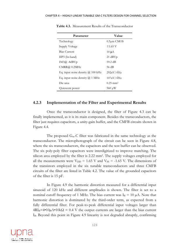
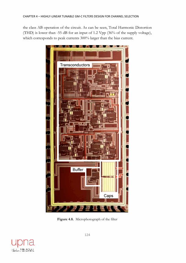
423 Implementation of the Filter and Experimental Results 123
xiii
43 Design of Channel Selection Filters for Bluetooth (2) 130
431 Simplification of the Topology 130
432 Commutation between BT and ZB modes 132
433 Tuning Control 135
44 Summary 146
Bibliography of the Chapter 147
`Uuml~eacuteiacuteEacuteecirc=`Uuml~eacuteiacuteEacuteecirc=`Uuml~eacuteiacuteEacuteecirc=`Uuml~eacuteiacuteEacuteecirc=5====liacuteUumlEacuteecirc=~eacuteeacuteaumlaacuteAring~iacuteaacuteccedilaringeumlliacuteUumlEacuteecirc=~eacuteeacuteaumlaacuteAring~iacuteaacuteccedilaringeumlliacuteUumlEacuteecirc=~eacuteeacuteaumlaacuteAring~iacuteaacuteccedilaringeumlliacuteUumlEacuteecirc=~eacuteeacuteaumlaacuteAring~iacuteaacuteccedilaringeuml====ccedilNtilde=Aringauml~eumleuml=^_=ccedilNtilde=Aringauml~eumleuml=^_=ccedilNtilde=Aringauml~eumleuml=^_=ccedilNtilde=Aringauml~eumleuml=^_=
iacuteecirc~aringeumlAringccedilaringCcediligraveAringiacuteccedilecirceumliacuteecirc~aringeumlAringccedilaringCcediligraveAringiacuteccedilecirceumliacuteecirc~aringeumlAringccedilaringCcediligraveAringiacuteccedilecirceumliacuteecirc~aringeumlAringccedilaringCcediligraveAringiacuteccedilecirceuml====153
51 Variable Gain Amplifier Cherry-Hooper Circuit 155
52 One-Stage Variable Gain Amplifier 157
521 Proposed VGA Scheme 157
522 Bandwidth Invariance with Gain 161
523 Process and Temperature Variations 162
524 Simulation Results 163
525 Measurement Results 166
53 Three-Stage VGA with Offset Control 171
531 Three-Stage VGA 171
532 Offset Control 173
54 Summary 182
Bibliography of the Chapter 183
`Uuml~eacuteiacuteEacuteecirc=`Uuml~eacuteiacuteEacuteecirc=`Uuml~eacuteiacuteEacuteecirc=`Uuml~eacuteiacuteEacuteecirc=6====`ccedilaringAringaumligraveeumlaacuteccedilaringeuml=~aringCcedil=cigraveiacuteigraveecircEacute=tccedilecircacirc`ccedilaringAringaumligraveeumlaacuteccedilaringeuml=~aringCcedil=cigraveiacuteigraveecircEacute=tccedilecircacirc`ccedilaringAringaumligraveeumlaacuteccedilaringeuml=~aringCcedil=cigraveiacuteigraveecircEacute=tccedilecircacirc`ccedilaringAringaumligraveeumlaacuteccedilaringeuml=~aringCcedil=cigraveiacuteigraveecircEacute=tccedilecircacirc==== 187
61 Conclusions 187
62 Future Work 189
`Uuml~eacuteiacuteEacuteecirc=`Uuml~eacuteiacuteEacuteecirc=`Uuml~eacuteiacuteEacuteecirc=`Uuml~eacuteiacuteEacuteecirc=7====`ccedilaringAringaumligraveeumlaacuteccedilaringEacuteeuml=oacute=i`ccedilaringAringaumligraveeumlaacuteccedilaringEacuteeuml=oacute=i`ccedilaringAringaumligraveeumlaacuteccedilaringEacuteeuml=oacute=i`ccedilaringAringaumligraveeumlaacuteccedilaringEacuteeuml=oacute=iinfinaringEacute~euml=cigraveiacuteigraveecirc~eumlinfinaringEacute~euml=cigraveiacuteigraveecirc~eumlinfinaringEacute~euml=cigraveiacuteigraveecirc~eumlinfinaringEacute~euml=cigraveiacuteigraveecirc~euml==== 193
71 Conclusiones 193
72 Liacuteneas Futuras 195
iiiiaacuteeumliacute=ccedilNtilde=aacuteeumliacute=ccedilNtilde=aacuteeumliacute=ccedilNtilde=aacuteeumliacute=ccedilNtilde=eacuteigraveAumlaumlaacuteAring~iacuteaacuteccedilaringeumleacuteigraveAumlaumlaacuteAring~iacuteaacuteccedilaringeumleacuteigraveAumlaumlaacuteAring~iacuteaacuteccedilaringeumleacuteigraveAumlaumlaacuteAring~iacuteaacuteccedilaringeuml 198
xiv
xv
ifpq=lc=^`olkvjpifpq=lc=^`olkvjpifpq=lc=^`olkvjpifpq=lc=^`olkvjp====
^Aringecircccedilaringoacuteatilde^Aringecircccedilaringoacuteatilde^Aringecircccedilaringoacuteatilde^Aringecircccedilaringoacuteatilde==== paacuteOumlaringaacuteNtildeaacuteAring~aringAringEacutepaacuteOumlaringaacuteNtildeaacuteAring~aringAringEacutepaacuteOumlaringaacuteNtildeaacuteAring~aringAringEacutepaacuteOumlaringaacuteNtildeaacuteAring~aringAringEacute====
AD AnalogDigital
AC Alternating Current
ACG Automatic Gain Control
ADSL Asymmetric Digital Subscriber Line
BJT Bipolar-Junction Transistor
BW Bandwidth
CCII Second-generation Current Conveyor
CMC Common-Mode-Control
CMFB Common-Mode Feedback
CMOS Complementary Metal-Oxide-Semiconductor
CMRR Common-Mode Rejection Ratio
DA DigitalAnalog
DC Direct Current
DVB Digital Video Broadcasting
EPROM Erasable Programmable Read-Only Memory
FGMOS Floating-Gate Metal-Oxide-Semiconductor
FG Floating-Gate
FGT Floating-Gate Transistor
FoM Figure of Merit
GB Gain-Bandwidth Product
Gm-C Transconductor-Capacitor
IF Intermediate Frequency
xvi
IM3 3rd -order Intermodulation Distortion
LAN Local Area Network
MOS Metal-Oxide-Semiconductor
MOSFET Metal-Oxide-Semiconductor Field-Effect-Transistor
MOSFET-C MOSFET- Capacitor
nMOS Negative-Channel Metal-Oxide-Semiconductor
opamp Operational Amplifier
OTA Operational Transconductance Amplifier
PCB Printed Circuit Board
pMOS Positive-Channel Metal-Oxide-Semiconductor
PpP Power-per-Pole
PSRR- Negative Power-Supply-Rejection-Ratio
PSRR+ Positive Power-Supply-Rejection-Ratio
QFG Quasi-Floating-Gate
QFGMOS Quasi-Floating-Gate Metal-Oxide-Semiconductor
QFGT Quasi-Floating-Gate Transistor
RSSI Received Signal Strength Indication
SFDR Spurious-Free Dynamic Range
SNR Signal-to-Noise Ratio
THD Total Harmonic Distortion
UV Ultraviolet
V-I Voltage-Intensity
VDSL Very high bit-rate Digital Subscriber Line
VGA Variable Gain Amplifier
VLSI Very-Large-Scale Integration
WiMAX Worldwide Interoperability for Microwave Access
xvii
m^o^jbqbo=dilpm^o^jbqbo=dilpm^o^jbqbo=dilpm^o^jbqbo=dilppppp^ov^ov^ov^ov====
m~ecirc~atildeEacuteiacuteEacuteecircm~ecirc~atildeEacuteiacuteEacuteecircm~ecirc~atildeEacuteiacuteEacuteecircm~ecirc~atildeEacuteiacuteEacuteecirc==== paacuteOumlaringaacuteNtildeaacuteAring~aringAringEacutepaacuteOumlaringaacuteNtildeaacuteAring~aringAringEacutepaacuteOumlaringaacuteNtildeaacuteAring~aringAringEacutepaacuteOumlaringaacuteNtildeaacuteAring~aringAringEacute====
CGB Gate-Bulk capacitance
CGD Gate-Drain capacitance
CGS Gate-Source capacitance
Cox Gate Oxide capacitance per unit area
fc Cutoff frequency
gm MOS transistor transconductance defined as partIDpartVGS
Gm Total transconductance of an OTA or transconductor
IB Bias current
iD MOS transistor drain current
K 1) Current scaling factor
2)MOS transistor transconductance coefficient
KB Boltzmann constant (138middot10-23 JK)
L Channel length of a MOS transistor
n Subthreshold slope factor
Pn Input-referred noise power
q Electron charge
r Channel resistance of a triode transistor
Q0 Initial electric charge
T Temperature
UT Thermal voltage
VCM Common-mode voltage
xviii
Vcn Bias voltage in an nMOS cascode transistor
Vcp Bias voltage in a pMOS cascode transistor
VDD Positive supply voltage
VSD VDS Source-drain Drain-source voltage of a MOS transistor
VSG VGS Source-gate Gate-source voltage of a MOS transistor
VSS Negative supply voltage
Vt Threshold voltage of a MOS transistor
W Channel width of a MOS transistor
micron Electron mobility parameter
1
`Uuml~eacuteiacuteEacuteecircUuml~eacuteiacuteEacuteecircUuml~eacuteiacuteEacuteecircUuml~eacuteiacuteEacuteecirc
====
1====
Introduction
The aim of this introductory chapter is to present the framework of the
thesis Section 11 is focused on the motivations of the thesis emphasizing the
growing importance of low-voltage low-power design applied to analog circuits
and particularly to channel selection filters In fact a review of the most
significant low-voltage and low-power analog design techniques is performed in
Section 111 as well as a discussion about the state of the art of the design of
Gm-C continuous-time channel selection filters in 112 General objectives of the
thesis are covered in Section 12 and finally a summary of the structure of the
work is provided in Section 13
11 Motivation
In the last decades there has been a growing demand of low-voltage
high-integrated electronic devices which meets the increasing requirements of
modern wireless and wireline communication systems powered by batteries The
goal is for these systems to be small and light as well as achieving long lifetime
for their batteries Hence the reduction of their power consumption becomes a
priority
Furthermore as the VLSI technology is led by the CMOS processes the
growing density of integration in CMOS technologies is reducing the thickness of
the gate oxide of transistors leading to a reduction of the supply voltage of the
CHAPTER 1 ndash INTRODUCTION
2
designs for reliability reasons and to avoid an excess of electric field intensity in
the devices [1] In addition it increases the driving capability of the transistor In
the 90s the supply voltage evolved from 5V to 33V and even voltages of 18V or
12 V were employed in 130nm CMOS technologies In more modern
technologies such as 90nm and 65nm voltages of 09V [2] are used and
according to SIA Roadmap predictions [3] the tendency is for the supply voltage
to keep decreasing Figure 11 illustrates how process-parameters have changed
over time by studying 14 different processes ranging from 30microm down to
007microm (Lmin) [4]
For technologies larger than 08microm Vdd stays flat and equal to 5V In
smaller technologies Vdd scales roughly linear with minimum feature size
following a staircase function Oxide thickness Tox scales down linearly with
technology And finally threshold voltage Vth scales more or less like a square
root function
Figure 11 Supply Voltage (Vdd) Threshold Voltage (Vth) and Oxide Thickness (Tox) as a
function of Technology geometry (Lmin)[4]
As a consequence of the drastic reduction of the power supplies they
are getting close to the threshold voltages of the MOS transistors as it is shown
in Figure 11 and in such a case digital techniques offer clear benefits with
respect to analog ones [5] Thanks to the way digital signals are processed CMOS
digital circuits have perfectly adapted themselves to these new tendencies Their
level of performance (speed) increases while at the same time the cost (power
CHAPTER 1 ndash INTRODUCTION
3
consumption and die area) decreases since they scale with supply voltage
However issues such as power density and leakage become important On the
other hand the performance of analog or mixed-signal circuits in newer CMOS
generations does not necessarily improve The most employed solution for
combined analog-digital designs where compatibility between analog and digital
blocks is required has been integrating together on the same chip both analog
and digital parts so that they share the same power supply rail Thus the
complexity involved in generating various supply voltages can be avoided [6]
However as opposed to digital case CMOS analog circuits using conventional
techniques suffer from degradation in terms of both dynamic range and signal-to-
noise ratio when a reduction of voltage supplies takes place [7] [8] Therefore
some alternative techniques for analog signal processing are needed
Furthermore although digital circuits are easier to design offer much
more robustness and flexibility than analog topologies and its electronic is more
versatile in terms of tuning and programmability there are still some applications
where analog electronics is either the most economical and suitable solution or
even the only alternative For instance interface circuits require a basic analog
processing as physical signals received from the environment are analog and thus
have to be minimally treated and adapted for digital processing and similarly
digital signals have to be converted to be delivered back to the analog world
Under the above conditions research on new solutions for low supply
voltage (twice the threshold voltage of a transistor or even lower) and low power
operation is a priority in the design of analog and mixed-signal wireless terminals
Aimed by this need in this work integrated analog circuits able to provide
innovative solutions for the baseband processing of short-distance wireless
receivers are going to be designed and fabricated Some applications are aimed to
creation of intelligent environments like a house or a car wireless connectivity of
devices like PCs or remote medical monitoring For that reason their
implementation becomes a technological challenge as it combines the necessity of
low voltage low power and high performance
Among the different blocks that can be employed in analog design
following these trends an important subset is filters Filters can be useful for
many applications in a system such as antialiasing and reconstruction channel
selection or noise reduction Specifically among them this thesis is focused on
the application of low-voltage low-power techniques to the design of high-
performance continuous-time filters for channel selection which are a key
element of modern wireless and wireline communication systems Their purpose
CHAPTER 1 ndash INTRODUCTION
4
is to discriminate the signal in the desired channel from other undesired signals in
adjacent channels interferences and out-of-band noise Large interferers near the
desired signal usually demand high linearity which is often difficult to achieve
together with low area and low power consumption
Traditionally active-RC filters have been widely employed due to their
high linearity (typical THD levels achieved are around -80 dB) [9] and to their
high Signal-to-Noise ratio (SNR) However their main drawback is their limited
bandwidth (a few MHz) consequence of the closed-loop operation of the
amplifiers This is due to the classic method followed by active RC topologies for
designing stable linear active circuits by means of feedback using passive linear
elements Another proposal for the design of continuous-time active filters are
MOSFET-C filters [10] based on the use of an equivalent CMOS tunable resistor
in an RC structure [11] [12] Similar to traditional active-RC configurations their
use is limited to low-frequency applications due to the requirements of high-
performance op-amps Moreover their supply voltage is usually constrained by
the requirement to tune the active resistors in a wide range
Current trends in modern communication systems lead to using more
elaborated modulation schemes with higher data rates hence requiring large
bandwidth and high linearity for the receiver front-end circuits and analog filters
which makes these classical op-amp based filters unsuitable For instance several
communication systems like ADSL VDSL 80211agn wireless LANs WiMax
LTE and DVB use various types of multicarrier modulation schemes All of them
have in common the use of multiple carriers over a wide bandwidth to provide
robustness against the impairments of poor quality wireless and wired
communication channels In order to avoid intermodulation distortion among the
multiple carriers [13ndash16] high linearity is required in the entire bandwidth of
these systems For instance ADSL requires an IM3 better than -60 dB in a signal
band of 11 MHz which extends to 4 MHz in ADSL2+ and up to 12 MHz in
very high-bit-rate DSL (VDSL) systems [17]
Furthermore besides these systems that use multicarrier modulation
schemes other systems with other modulation techniques have also special needs
that cannot be covered with traditional filter topologies For instance the
receivers employed in Wireless Personal Area Networks (WPAN) Bluetooth
based on standard IEEE 802151 and Zigbee based on standard IEEE 802154
are the most popular technologies employed in these systems Bluetooth is a
wireless technology standard for exchanging data over short distances using
short-wavelength radio transmissions in the ISM band from 2400ndash2480 MHz
CHAPTER 1 ndash INTRODUCTION
5
from fixed and mobile devices creating personal area networks with high levels
of security [18] It uses a radio technology called frequency-hopping spread
spectrum (FHSS) and its latest versions achieve data rates larger than 1Mbps
ZigBee is a low-cost low-power wireless mesh network standard The low cost
allows the technology to be widely deployed in wireless control and monitoring
applications and the low power-usage allows longer life with smaller batteries [19]
It has a maximum defined rate of 250 kbps and uses also the ISM 24 GHz band
as well as the 868915MHz bands It is mainly used in applications that require a
low data rate long battery life and secure networking It employs direct-sequence
spread spectrum (DSSS) coding Although the modulation techniques of these
standards require less bandwidth and linearity than those of the multicarrier
systems these requirements must be obtained in this case with much lower power
levels making useful again high linearity low consumption approaches
An up-to-date proposal more appropriate for all these modern systems
is based on using Gm-C topologies ie filters based on transconductors and
capacitors [20ndash23] These filters are simple and feature tuning capability and
higher operating frequencies Due to their open-loop operation they usually
achieve lower power consumption for a given bandwidth but they also feature
less linearity than the other approaches[24] [25] This limitation can be avoided
by coming back to the classic approach negative feedback and passive resistors
to achieve highly linear circuits while designing the transconductor Thanks to
this a highly linear voltage to current (V-I) conversion can be achieved As a
consequence the linearity levels obtained can be compared to those of active-RC
filters [26] [27]
Precisely the implementation of Gm-C channel selection filters is the
main topic of this thesis As it has been said before in order to be adapted to
modern wireless receiver requirements the resulting circuits need to achieve high-
linearity and be implemented by using low-voltage low-power techniques
111 Low-Voltage Low-Power Techniques
Since the beginning of the 90s an intense research in low-voltage
andor low-power circuits has been developed growing continuously since then
In fact from the mid-90s it has been a very current topic in literature either in
books or analog design journals [28ndash34] It must be noted that in spite of being
usually joined in titles Low-voltage and Low-power are terms generally opposed
in analog design [8] making indispensable the use of low-power techniques [35]
to approach a very low-voltage design
CHAPTER 1 ndash INTRODUCTION
6
There are different viewpoints to study these techniques Solutions
based on novel cells modification of classical architectures or new methods of
signal processing are some of them A general overview of these techniques
applied to analog design is presented in this Section
Regarding cell design it is remarkable the very low-voltage current
mirror proposed in [36] Considering op-amp design the impossibility of
employing complementary stages at the op-amp input is not a serious problem
when the amplifier has an inverter configuration since a differential pair can be
employed (eg a PMOS) keeping the common-mode input voltage of the
amplifier very close to one of the supply voltages (the lowest one for the PMOS
case) of the circuit By using a periodic charge injection in SC circuits [37] [38] or
a DC level shift in continuous-time circuits [39] the difference between the
common-mode voltages at the input and the output of the op-amp that allows a
maximum output voltage range can be solved However in non-inverter circuits
a technique to remove the common-mode component of an input differential
signal is proposed in [40] and the same effect is achieved in [41] [42] in a more
efficient and simpler way
At this cell level new concepts have been developed in the past few
years aiming to have great impact reducing voltage and power in analog and
mixed-mode circuits Among them Floating Gate and Quasi-Floating Gate
techniques deeply explained in Chapter 2 are going to have a special relevance in
this thesis QFG techniques are based on using MOS devices with one or multiple
inputs capacitively coupled to the gate terminal (like the Floating Gate devices
also explained in Chapter 2) but with the DC operating point set by a large
resistor These techniques allow eliminating the offset caused during fabrication
as well as achieving less area and a great potential for class AB operation Some
examples of the use of these techniques in common circuits like op-amps OTAs
or multipliers are [43ndash47]
Considering the reduction of power consumption class AB stages have
become very popular and even necessary in low-power circuits They allow
obtaining large Slew-Rate values for large-signal operation with low bias currents
so keeping low static power consumption An interesting way of obtaining class
AB operation in the output stages is by means of the already mentioned QFG
techniques This proposal is covered in Chapter 2 as well and is applied in several
papers like [26] [48ndash50]
CHAPTER 1 ndash INTRODUCTION
7
In relation to this class AB operation super-class AB amplifiers have
been recently proposed [51ndash53] This concept is applied to one-stage amplifiers
where class AB operation has been achieved both in the input differential pair
and in the active load By means of this technique the obtained slew-rate is
similar to conventional class AB amplifiers while the static power consumption is
reduced by one order of magnitude obtaining a power efficiency close to 100
Another interesting topic widely researched lately is the use of MOS
transistors operating in moderate inversion [54ndash56] By operating in this region
good performance in low-power circuits is obtained in terms of linearity
bandwidth and noise Significant advantages can be obtained by combining both
moderate (or even weak) inversion operation and FG or QFG configurations in a
transistor
Considering sub-system level some remarkable contributions exist in
the field of the SC circuits such as the switched-opamp method proposed in [57]
[58] based on the replacement of the critical switches of the conventional
switched-capacitor technique with opamps which are turned on and off resulting
in a true very low voltage operation Another example is the employment of
techniques of clock-amplification using the circuit presented in [59] Moreover
companding techniques are also interesting nowadays in order to compensate for
the reduction of the dynamic range in some circuits [60] [61] Companding
consists in exploiting the non-linear behavior of basic devices like transistors
compensating globally their non-linearities allowing in such a way for the biasing
to set close to the limits imposed by the technology Besides by using this
technique wide current swings can be achieved with small voltage variations
improving speed and reducing supply voltage requirements [62] These techniques
have been validated in several circuits such as strong or weak inversion MOS
circuits or bipolar topologies [63ndash65]
Furthermore both in cell design and in systems or subsystems design
general current-mode techniques must also be highlighted [66ndash69] and more
interesting for low-power designs are the ones using transistors in weak inversion
region [70ndash72]
Finally some examples of contributions at system level include trying to
reduce supply voltages or power consumption improvements done in the field of
AD converters It is necessary to choose the appropriate architecture [73] and in
order to achieve the required dynamic range in a compact and power-efficient
way the choice of Sigma-Delta converters [74] [75] and their implementation
CHAPTER 1 ndash INTRODUCTION
8
with a very low supply voltage [33] is almost mandatory Other proposals also
useful for low-voltage designs due to their efficiency in terms of power
consumption are [76] [77]
112 Gm-C Filters
As it has been already said in this Section Gm-C filters have replaced
progressively classic MOSFET-C and RC realizations in many applications due to
their wider frequency response despite the drawback of the poor linearity
inherent to traditional OTAs Precisely as specified before the implementation
of Gm-C filters is the goal of this thesis Obviously in order to be competitive in
the target application linearity of Gm-C filters must increase by means of several
techniques like input attenuation or source degeneration or another one of the
methods explained later in Chapter 3 [78]
First of all Gm-C filters have needed to adapt themselves to the
previously presented changes that technology and power supply have suffered
over the years For instance while at the beginning of the 90s filters were
implemented with technologies like CMOS 09 microm [79] or high power supplies
like 10V [80] actual filters employ more modern technologies like CMOS 90 nm
[81] and lower power supplies like 1V [21]
Regarding linearity improvement Gm-C filters have used different
approaches over the years achieving performances comparable to those of RC
configurations Many filter topologies increase their linearity thanks to the source
degeneration technique like [17] [23] [27] [79] [82ndash92] Among them [17] [27]
[82] [87] [88] [90] employ passive resistors in their designs which perform the V-
I conversion while other proposals like [79] [84ndash86] make use of triode
transistors in order to degenerate the source Other circuits use mixed source
degeneration structures formed by both passive resistors and MOS transistors in
triode region [23] [89] [92] achieving at the same time high linearity and
tunability It must be noted that the first reference to the use of common-mode
sensing by two matched degeneration devices can be found in [85] Another
method to linearize a filter also explained deeply in Chapter 3 is the adaptive
biasing employed in filters like [93] [94] A combination of both linearization
techniques can be seen in [83] Lastly it is also interesting to note that some
topologies like the ones proposed in [80] [87] [90] use passive feedback
components as for the active RC configurations so the resulting filters are
considered as hybrids between Gm-C filters and active RC circuits providing a
good tradeoff between linearity and bandwidth
CHAPTER 1 ndash INTRODUCTION
9
Moreover by analyzing the state-of-the-art of Gm-C filters some
topologies already employing Floating Gate and Quasi Floating Gate techniques
in their designs can be discovered On the one hand some proposals like [17]
present a FGMOS as input transistor showing an improvement of linearity up to
10 dB in comparison with an equivalent circuit without FGMOS In [46] [55]
[95] [96] FGMOS transistors have also been used in the design of multiple-input
transconductors as a way to finally implement very low-power filters On the
other hand QFG techniques have also been used in some topologies such as [97]
in order to linearize triode transistors in source degeneration structures and
achieve an ideal cancellation of the non-linear terms of the equivalent resistor
Proposals like [98] [99] also use QFG transistors in their implementation Article
[100] shows how to apply FG and QFG techniques in different circuit
implementations and the advantages they provide Besides these interesting
techniques other strategies also mentioned in the previous Section have been
applied to transconductor blocks at transistor level in order to achieve low-
voltage low-power operation in Gm-C topologies [36] [101ndash103]
Considering the topology and the design of Gm-C filters several
strategies can be followed including the biquad cascade [86] [104] LC ladder
simulation -substituting passive inductances by gyrators- [20] and multiple loop
feedback [105] The following books about filter designs propose different
techniques [25] [106] [107]
Finally regarding tuning different methods have been employed over
the years in Gm-C filters design While some topologies choose discrete
frequency tuning configurations like capacitor arrays [92] [108] or switchable
transconductors [109] [110] other filters use continuous tuning schemes instead
Different continuous approaches can be discovered by looking throughout the
literature such as tuning based on multipliers [80] transconductance tuning by
external resistors in charge of setting the bias currents [44] [88] [91] or manual
tuning by changing directly the bias current [111] [112] Another proposal of
great relevance for this work consists in implementing a resistive divider with
triode transistors in order to tune the circuit This idea firstly proposed in [90]
has also been used in [17] [82] [83] Furthermore in some cases automatic tuning
circuitry is also included on the same chip in fully integrated Gm-C filter design
in order to overcome the effects of parameter drift due to the process
temperature and environment variations or aging Among others Master-Slave
automatic tuning with VCO or methods based on charge balancing and Gm-C
CHAPTER 1 ndash INTRODUCTION
10
integrators have been employed ([20] [23] [79] [85] [87] [90] [104] [110] [113ndash
115])
12 Objectives
According to what has been said so far the general purpose of this
thesis is to develop circuits and techniques for Gm-C filter design focusing the
efforts on achieving for them low-voltage and low-power operation In particular
the objectives of this work are the following
At cell level
At this level the first objective is to summarize the state-of-the-art of
the main low-power low-voltage techniques employed so far in the literature
Mainly this analysis is going to be focused on techniques based on Floating Gate
(FG) and Quasi-Floating Gate (QFG) transistors
To apply these low-power low-voltage techniques in order to design
basic cells -transconductors mainly- suitable for Gm-C filter design Special
attention must be paid when these techniques are applied to the performance of
the circuits particularly in terms of power consumption and linearity
To develop a systematic approach to implement high-performance
CMOS tunable transconductors able to fulfill the challenging requirements of
current analog design
At system level
To perform a general overview of different wireless receiver
configurations paying special attention to homodyne receivers which are going
to include in their implementation the circuits proposed in this work
To summarize the advantages and drawbacks of using Gm-C filter
topologies in modern communication systems as well as provide solutions to
CHAPTER 1 ndash INTRODUCTION
11
overcome the issues they present The evolution suffered by this type of filters in
analog design must also be studied
To implement a tunable highly linear third-order Butterworth low-pass
Gm-C filter suitable for both Bluetooth and Zigbee applications by employing
some of the techniques at both basic cell and system level proposed throughout
this work
To propose some Automatic Tuning Systems appropriate to be used
along with the implemented filter in order to make it more practical and better
adapted to current necessities
To implement other important blocks of the receiver by means of the
previously obtained transconductor and the low-voltage low-power techniques
like the VGA An offset-cancellation circuit is usually necessary when the VGA
presents multiple stages
By fulfilling these objectives this thesis tries to contribute to low-voltage
low-power continuous-time filtering at both cell and system level which is one of
the most important trends in analog design due to the huge proliferation of
wireless devices as well as to wireless reception in general by implementing other
necessary low-power blocks All the circuits developed in this work have been
fabricated and tested using a 05microm n-well CMOS technology
13 Structure of the Thesis
This thesis is organized in six chapters being the first one the present
introductory chapter It has been focused on explaining the motivations of this
work along with an overview of low-voltage low-power techniques and a
summary of the state-of-the-art of Gm-C filter design Besides the objectives of
the thesis have been established The following paragraphs provide a summary of
the other five chapters of this work
Chapter 2 covers the concept of Floating Gate (FG) and Quasi-Floating
Gate (QFG) transistors These two devices are analyzed in detail in this chapter
as well as several techniques based on them Some applications where these
CHAPTER 1 ndash INTRODUCTION
12
techniques are employed are also presented This chapter is particularly relevant
for this thesis as many of the proposed techniques are going to be applied
throughout it in order to achieve low-voltage and low-power operation but also
to provide tuning capability or linearity improvement
Chapter 3 is devoted to the design technique of high-performance
CMOS transconductors challenging nowadays due to the restrictions imposed by
technology downscaling and low power requirements To overcome these current
issues techniques presented in Chapter 2 are going to be employed in the design
Several circuit configurations are proposed throughout this chapter By having
their performances compared the most suitable ones to implement a proper
transconductor can be chosen In fact this chapter also provides a systematic
approach to implement suitable transconductors for wireless receivers resulting
in a new family of cells featuring high linearity in a wide input range class AB
operation and continuous tuning
In Chapter 4 focused on Gm-C filter design a wide range tunable
highly linear third order Butterworth low-pass Gm-C filter is implemented and
fabricated using the systematic approach proposed in the previous chapter to
obtain its basic cell a class AB programmable transconductor QFG techniques
are also employed in the design Measurements results can be found in this
chapter Furthermore an optimized version in terms of area of this Gm-C filter is
implemented as well Lastly two Automatic Tuning Systems are proposed to
operate along with the filter making it more practical
Chapter 5 is devoted to implement other important blocks of a wireless
receiver employing for it the basic transconductor cell previously proposed and
verified According to this goal a Variable Gain Amplifier (VGA) is proposed
fabricated and measured This circuit operates with constant bandwidth for all the
gain settings Moreover from the experimentally validated one-stage VGA a
three-stage VGA is also proposed The aim of this new circuit is to achieve a
larger gain tuning range than the basic one Nevertheless an offset-cancellation
circuit is now necessary and must be added A proposal is included to this aim
Finally Chapter 6 provides a compilation of the most significant results
and general conclusions of this work Besides future research lines related to this
thesis are proposed and briefly analyzed
CHAPTER 1 ndash INTRODUCTION
13
Bibliography of the Chapter
[1] C J B Fayomi M Sawan and G W Roberts ldquoReliable circuit techniques for low-voltage analog design in deep submicron standard CMOS a tutorialrdquo Analog Integrated Circuits and Signal Processing vol 39 no 1 pp 21ndash38 Apr 2004
[2] J M Algueta ldquoHigh performance tunable CMOS continous-time filtersrdquo PhD Thesis UPNA 2012
[3] ldquohttppublicitrsnetrdquo Semiconductor Industry Association (SIA) Roadmap 2012
[4] K Bult ldquoAnalog design in deep sub-micron CMOSrdquo Proc European Solid-State Conference 1999
[5] B P Lathi and Z Ding Modern digital and analog communication systems New York Oxford University Press 2009
[6] J Ramirez-Angulo R G Carvajal and A Lopez-Martin ldquoTechniques for the design of low voltage power efficient analog and mixed signal circuitsrdquo 22nd International Conference on VLSI Design pp 26ndash27 Jan 2009
[7] M Steyaert V Peluso J Bastos P Kinget W Sansen K U Leuven and K Mercierlaan ldquoCustom analog low power design the problem of low voltage and mismatchrdquo Proc IEEE- Custom Int Circ Conf CICC97 pp 285ndash292 1997
[8] A-J Annema ldquoAnalog circuit performance and process scalingrdquo IEEE Transactions on Circuits and Systems II Analog and Digital Signal Processing vol 46 no 6 pp 711ndash725 Jun 1999
[9] A M Durham W Redman-White and J B Hughes ldquoHigh-linearity continuous-time filter in 5-V VLSI CMOSrdquo IEEE Journal of Solid-State Circuits vol 27 no 9 pp 3ndash9 1992
[10] Y Tsividis and J O Voorman Integrated continuous-time filters New York IEEE Press 1993
[11] Y Tsividis ldquoContinuous-time MOSFET-C filters in VLSIrdquo IEEE Journal of Solid-State Circuits vol sc-21 no 1 pp 15ndash30 1986
CHAPTER 1 ndash INTRODUCTION
14
[12] M Banu and Y Tsividis ldquoFully integrated active RC filters in MOS technologyrdquo IEEE Journal of Solid-State Circuits vol sc-18 no 6 pp 644ndash651 1983
[13] N Tan F Caster C Eichrodt S O George B Horng and J Zhao ldquoA universal quad AFE with integrated filters for VDSL ADSL and GSHDSLrdquo Proc IEEE Custom Integrated Circuits Conference (CICC2003) pp 599ndash602 2003
[14] Very-high-bit-rate digital subscriber line (VDSL) metallic interface T1E14 ANSI document 2001
[15] H Weinberger A Wiesbauer C Fleischhacker and J Hauptmann ldquoA 800mW full-rate ADSL-RT analog frontend IC with integrated line driverrdquo IEEE Conf Custom Integrated Circuits 2001 pp 115ndash118 2001
[16] M Moyal M Groepl H Werker G Mitteregger and J Schambacher ldquoA 700 900mW channel CMOS dual analog front-end IC for VDSL with integrated 115 145dBm line driversrdquo IEEE International Solid State Circuits Conference Digest of Technical Papers vol 23 no 236 2003
[17] J Chen E Saacutenchez-Sinencio and J Silva-Martinez ldquoFrequency-dependent harmonic-distortion analysis of a linearized cross-coupled CMOS OTA and its application to OTA-C filtersrdquo IEEE Transactions on Circuits and Systems I Regular Papers vol 53 no 3 pp 499ndash510 2006
[18] ldquohttpwwwbluetoothcomPagesBluetooth-Homeaspxrdquo
[19] ldquohttpwwwzigbeeorgHomeaspxrdquo
[20] B Guthrie J Hughes T Sayers and A Spencer ldquoA CMOS gyrator low-IF filter for a dual-mode BluetoothZigBee transceiverrdquo IEEE Journal of Solid-State Circuits vol 40 no 9 pp 1872ndash1879 Sep 2005
[21] T Lo and C Hung ldquoMultimode GmndashC channel selection filter for mobile applications in 1-V supply voltagerdquo IEEE Transactions on Circuits and Systems II Express Briefs vol 55 no 4 pp 314ndash318 2008
CHAPTER 1 ndash INTRODUCTION
15
[22] C I Lujan-Martinez R G Carvajal A Torralba A J Lopez-Martin J Ramirez-Angulo and U Alvarado ldquoLow-power baseband filter for zero-intermediate frequency digital video broadcasting terrestrialhandheld receiversrdquo IET Circuits Devices amp Systems vol 3 no 5 pp 291ndash301 2009
[23] F Behbahani W Tan A Karimi-Sanjaani A Roithmeier and A A Abidi ldquoA broad-band tunable CMOS channel-select filter for a low-IF wireless receiverrdquo IEEE Journal of Solid-State Circuits vol 35 no 4 pp 476ndash489 2000
[24] S Kousai M Hamada R Ito and T Itakura ldquoA 197 MHz fifth-order active-RC chebyshev LPF for draft IEEE 80211n with automatic quality-factor tuning schemerdquo IEEE Journal of Solid-State Circuits vol 42 no 11 pp 2326ndash2337 2007
[25] Y Sun ldquoDesign of high-frequency integrated analogue filtersrdquo IET Circuits Devices and Systems Series 14 2002
[26] C Garcia-Alberdi A J Lopez-Martin L Acosta R G Carvajal and J Ramirez-Angulo ldquoTunable class AB CMOS Gm-C filter based on quasi-floating gate techniquesrdquo IEEE Transactions on Circuits and Systems I Regular Papers vol 60 no 5 pp 1300ndash1309 2013
[27] L Acosta M Jimeacutenez R G Carvajal A J Lopez-Martin and J Ramiacuterez-Angulo ldquoHighly linear tunable CMOS Gm-C low-pass filterrdquo IEEE Transactions on Circuits and Systems I Regular Papers vol 56 no 10 pp 2145ndash2158 2009
[28] E Saacutenchez-Sinencio and A G Andreou (eds) Low-voltagelow-power integrated circuits and systems NJ IEEE Press 1999
[29] W Serdijn A C Van der Woerd and J C Kuenen (eds) ldquoSpecial issue on low-power analog integrated circuitsrdquo Analog Integrated Circuits and Signal Processing 1995 vol 8 1995
[30] S Yan and E Sanchez-Sinencio ldquoLow voltage analog circuit design techniques a tutorialrdquo IEICE Transactions on Analog Integrated Circuits and Systems vol E00-A pp 1ndash17 2000
CHAPTER 1 ndash INTRODUCTION
16
[31] J H Huijsing M J Hogervost M J Fonderie K J de Langen B J van der Dool and G Groenewold ldquoLow-voltage analog signal processingrdquo in Analog VLSI Signal and Information Processing T Ismail M Fiez Ed New York McGraw-Hill 1993
[32] R Hogervost and J H Huijsing Design of low-voltage low-power operational amplifier cells Dordrecht The Netherlands Kluwer Academic 1996
[33] S Rabii and B A Wooley The design of low-voltage low-power sigma-delta modulators Kluwer Academic Publishers 1999
[34] R J Widlar ldquoLow voltage techniquesrdquo IEEE International Solid State Circuits Conference Digest of Technical Papers 1978 pp 238ndash239
[35] E Vittoz ldquoMicropower techniquesrdquo in Design of VLSI Circuits for Telecommunications and Signal Processing J Franca and Y Tsividis Eds Englewood Cliffs NJ Prentice-Hall 1993
[36] R Castello F Montecchi F Rezzi and A Baschirotto ldquoLow-voltage analog filtersrdquo IEEE Transactions on Circuits and Systems I Fundamental Theory and Applications vol 42 no 11 pp 827ndash840 1995
[37] A Baschirotto and R Castello ldquoA 1-V 18-MHz CMOS switched-opamp SC filter with rail-to-rail output swingrdquo IEEE Journal of Solid-State Circuits vol 32 no 12 pp 1979ndash1986 1997
[38] A Baschirotto R Castello and G P Montagna ldquoActive series switch for switched-opamp circuitsrdquo Electronics Letters vol 34 no 14 pp 1365ndash1366 1998
[39] J Ramirez-Angulo R G Carvajal J Tombs and A Torralba ldquoSimple technique for opamp continuous- time 1V supply operationrdquo Electronics Letters vol 35 no 4 pp 263ndash264 1999
[40] J Fonderie M M Maris E J Schnitger and J H Huijsing ldquo1-V operational amplifier with rail-to-rail input and output rangesrdquo IEEE Journal of Solid-State Circuits vol 24 no 6 pp 1551ndash1559 1989
[41] J F Duque-Carrillo J L Ausiacuten G Torelli J M Valverde and M A Domiacutenguez ldquo1-V rail-to-rail operational amplifiers in standard CMOS technologyrdquo IEEE Journal of Solid-State Circuits vol 35 no 1 pp 33ndash44 2000
CHAPTER 1 ndash INTRODUCTION
17
[42] J Ramirez-Angulo A Torralba R G Carvajal and J Tombs ldquoLow-voltage CMOS operational amplifiers with wide input-output swing based on a novel schemerdquo IEEE Transactions on Circuits and Systems I Fundamental Theory and Applications vol 47 no 5 pp 772ndash774 May 2000
[43] C-G Yu and R L Geiger ldquoVery low voltage operational amplifiers using floating gate MOS transistorrdquo 1993 IEEE International Symposium on Circuits and Systems pp 1152ndash1155
[44] K Yang and A G Andreou ldquoA multiple input differential amplifier based on charge sharing on a floating-gate MOSFETrdquo Analog Integrated Circuits and Signal Processing vol 6 pp 197ndash208 1994
[45] J Ramirez-Angulo R G Carvajal J Tombs and A Torralba ldquoLow-voltage CMOS op-amp with rail-to-rail input and output signal swing for continuous-time signal processing using multiple-input floating-gate transistorsrdquo IEEE Transactions on Circuits and Systems II Analog and Digital Signal Processing vol 48 no 1 pp 111ndash116 2001
[46] F Muntildeoz A Torralba R G Carvajal J Tombs and J Ramırez-Angulo ldquoFloating-gate-based tunable CMOS low-voltage linear transconductor and its application to HF Gm-C filter designrdquo IEEE Transactions on Circuits and Systems II Analog and Digital Signal Processing vol 48 no 1 pp 106ndash110 2001
[47] J Ramirez-Angulo R G Carvajal and J Martinez-Heredia ldquo14v supply wide swing high frequency CMOS analogue multiplier with high current efficiencyrdquo ISCAS 2000 - IEEE International Symposium on Circuits and Systems vol 2 pp 533ndash536
[48] A Lopez-Martin J M Algueta-Miguel L Acosta J Ramirez-Angulo and R Gonzaacutelez-Carvajal ldquoDesign of two-stage class AB CMOS buffers a systematic approachrdquo ETRI Journal vol 33 no 3 pp 393ndash400 Jun 2011
[49] J Ramiacuterez-Angulo R G Carvajal J A Galaacuten and A Loacutepez-Martiacuten ldquoA free but efficient low-voltage class-AB two-stage operational amplifierrdquo IEEE Transactions on Circuits and Systems II Express Briefs vol 53 no 7 pp 568ndash571 2006
CHAPTER 1 ndash INTRODUCTION
18
[50] A J Lopez-Martin J M Algueta C Garcia-Alberdi L Acosta R G Carvajal and J Ramirez-Angulo ldquoDesign of micropower class AB transconductors A systematic approachrdquo Microelectronics Journal pp 1ndash10 2012
[51] S Baswa J Ramırez-Angulo A J Lopez-Martin R G Carvajal and M Bikumandla ldquoRail-to-rail super class AB CMOS operational amplifiersrdquo Electronics Letters vol 41 no 1 pp 5ndash6 2005
[52] J A Galan A J Loacutepez-Martiacuten R G Carvajal J Ramiacuterez-Angulo and C Rubia-Marcos ldquoSuper class-AB OTAs with adaptive biasing and dynamic output current scalingrdquo IEEE Transactions on Circuits and Systems I Regular Papers vol 54 no 3 pp 449ndash457 2007
[53] A J Loacutepez-Martiacuten S Baswa J Ramirez-Angulo and R G Carvajal ldquoLow-voltage super class AB CMOS OTA cells with very high slew rate and power efficiencyrdquo IEEE Journal of Solid-State Circuits vol 40 no 5 pp 1068ndash1077 2005
[54] A J Lopez-Martin J Ramiacuterez-Angulo R Gonzaacutelez Carvajal and L Acosta ldquoCMOS transconductors with continuous tuning using FGMOS balanced output current scalingrdquo IEEE Journal of Solid-State Circuits vol 43 no 5 pp 1313ndash1323 2008
[55] J M Algueta Miguel A J Lopez-Martin J Ramirez-Angulo and R G Carvajal ldquoTunable rail-to-rail FGMOS transconductorrdquo Proceedings of 2010 IEEE International Symposium on Circuits and Systems pp 225ndash228 May 2010
[56] A J Lopez-Martin J Ramirez-Angulo and R G Carvajal ldquoLow-voltage FGMOS-based balanced current scaling in moderate inversionrdquo 18th European Conference on Circuit Theory and Design pp 56ndash59 Aug 2007
[57] J Crols and M Steyaert ldquoSwitched-opamp an approach to realize full CMOS switched-capacitor circuits at very low power supply voltagesrdquo IEEE Journal of Solid-State Circuits vol 29 no 8 pp 936ndash942 1994
[58] V Peluso P Vancorenland A M Marques S J Steyaert and W Sansen ldquoA 900-mV low-power AD converter with 77-dB dynamic rangerdquo IEEE Journal of Solid-State Circuits vol 33 no 12 pp 1887ndash1897 1998
CHAPTER 1 ndash INTRODUCTION
19
[59] J F Dickson ldquoOn-chip high-voltage generation in MNOS integrated circuits using an improved voltage multiplier techniquerdquo IEEE Journal of Solid-State Circuits vol SC-11 no 3 pp 374ndash378 1976
[60] Y Tsividis ldquoOn linear integrators and differentiators using instantaneous compandingrdquo IEEE Transactions on Circuits and Systems II Analog and Digital Signal Processing vol 42 no 8 pp 561ndash564 1995
[61] Y Tsividis ldquoGeneral approach to signal processors employing compandingrdquo Electronics Letters vol 31 no 18 pp 1549ndash1550 1995
[62] J Mulder A C Van der Woerd W A Serdijn and H M Van Roermund ldquoGeneral current-mode analysis method for translinear filtersrdquo IEEE Transactions on Circuits and Systems I Fundamental Theory and Applications vol 44 no 3 pp 193ndash197 Mar 1997
[63] J Mulder A C Van der Woerd W A Serdijn and A H M Van Roermund ldquoAn RMS-DC converter based on the dynamic translinear principlerdquo IEEE Journal of Solid-State Circuits vol 32 no 7 pp 1146ndash1150 Jul 1997
[64] J Mulder W A Serdijn A C Van der Woerd and A H M Van Roermund Dynamic translinear and log-domain circuits Kluwer Academic Publishers 1999
[65] D Perry and G W Roberts ldquoThe design of log-domain filters based on the operational simulation of LC laddersrdquo IEEE Transactions on Circuits and Systems II Analog and Digital Signal Processing vol 43 no 11 pp 763ndash774 1996
[66] G Han and E Saacutenchez-Sinencio ldquoCMOS transconductance multipliers a tutorialrdquo IEEE Transactions on Circuits and Systems II Analog and Digital Signal Processing vol 45 no 12 pp 1550ndash1563 1998
[67] T Kwan and K Martin ldquoAn adaptive analog continuous-time CMOS biquadratic filterrdquo IEEE Journal of Solid-State Circuits vol 26 no 6 pp 859ndash867 Jun 1991
[68] E Seevinck and R J Wiegerink ldquoGeneralized translinear circuit principlerdquo IEEE Journal of Solid-State Circuits vol 26 no 8 pp 1098ndash1102 1991
CHAPTER 1 ndash INTRODUCTION
20
[69] J Ramirez-Angulo S C Choi and G Gonzalez-Altamirano ldquoLow-voltage circuits building blocks using multiple-input floating-gate transistorsrdquo IEEE Transactions on Circuits and Systems I Fundamental Theory and ApplicationsCircuits and Systems I vol 42 no 11 pp 9ndash12 1995
[70] A G Andreou K A Boahen P O Pouliquen A Pavasovic R E Jenkins and K Strohbehn ldquoCurrent-mode subthreshold MOS circuits for analog VLSI neural systemsrdquo IEEE transactions on neural networks vol 2 no 2 pp 205ndash13 Jan 1991
[71] E Vittoz and J Fellrath ldquoCMOS analog integrated circuits based on weak inversion operationrdquo IEEE Journal of Solid-State Circuits vol sc-12 no 3 pp 224ndash231 1977
[72] C A Mead Analog VLSI and neural systems Reading MA Addison-Wesley 1989
[73] R Van de Plassche Integrated analog-to-digital and digital-to-analog converters Boston Kluwer Academic Publishers 1994
[74] J C Candy and G C Temes Oversampling delta-sigma data converters IEEE Press New York 1992
[75] S R Norsworthy R Schreier and G C Temes Delta-sigma data converters IEEE Press Piscattway NJ 1997
[76] F Colodro A Torralba F Muntildeoz and L G Franquelo ldquoNew class of multibit sigma-delta modulators using multirate architecturerdquo Electronics Letters vol 36 no 9 pp 783ndash785 2000
[77] F Colodro A Torralba A P Vegaleal and L G Franquelo ldquoMultirate-multibit sigma-delta modulatorsrdquo ISCAS 2000 - IEEE International Symposium on Circuits and Systems pp 10ndash13 2000
[78] E Sanchez-Sinencio and J Silva-Martinez ldquoCMOS transconductance amplifiers architectures and active filters a tutorialrdquo IEE Proceedings - Circuits Devices and Systems vol 147 no 1 p 3 2000
[79] J M Khoury ldquoDesign of a 15-MHz CMOS continuous-time filter with on-chip tuningrdquo IEEE Journal of Solid-State Circuits vol 26 no 12 1991
CHAPTER 1 ndash INTRODUCTION
21
[80] S D Willingham K W Martin and A Ganesan ldquoA BiCMOS low-distortion 8-MHz low-pass filterrdquo IEEE Journal of Solid-State Circuits vol 28 no 12 pp 1234ndash1245 1993
[81] A Pirola A Liscidini and R Castello ldquoCurrent-mode WCDMA channel filter with in-band noise shapingrdquo IEEE Journal of Solid-State Circuits vol 45 no 9 pp 1770ndash1780 2010
[82] A Lewinski and J Silva-Martinez ldquoOTA Linearity enhancement technique for high frequency applications with IM3 below -65dBrdquo IEEE Custom Integrated Circuits Conference pp 9ndash12 2003
[83] W Huang and E Saacutenchez-Sinencio ldquoRobust highly linear high-frequency CMOS OTA with IM3 below -70 dB at 26 MHzrdquo IEEE Transactions on Circuits and Systems I Regular Papers vol 53 no 7 pp 1433ndash1447 2006
[84] R Castello I Bietti and F Svelto ldquoHigh-frequency analog filters in deep-submicron CMOS technologyrdquo Proc IEEE ISSCC Dig Tech Papers pp 74ndash76 1999
[85] J Silva-Martiacutenez J Adut J M Rocha-Perez M Robinson and S Rokhsaz ldquoA 60-mW 200-MHz continuous-time seventh-order linear phase filter with on-chip automatic tuning systemrdquo IEEE Journal of Solid-State Circuits vol 38 no 2 pp 216ndash225 2003
[86] P Pandey J Silva-Martinez and X Liu ldquoA CMOS 140-mW fourth-order continuous-time low-pass filter stabilized with a class AB common-mode feedback operating at 550 MHzrdquo IEEE Transactions on Circuits and Systems I Regular Papers vol 53 no 4 pp 811ndash820 Apr 2006
[87] J Lee C C Tu and W Chen ldquoA 3V linear input range tunable CMOS transconductor and its application to a 33V 11MHz chebyshev low-pass Gm-C filter for ADSLrdquo IEEE Custom Integrated Circuits Conference pp 387ndash390 2000
[88] T Itakura T Ueno H Tanimoto A Yasuda R Fujimoto T Arai and H Kokatsu ldquoA 27-V 200-kHz 49-dBm stopband-IIP3 low-noise fully balanced gm-C filter ICrdquo IEEE Journal of Solid-State Circuits vol 34 no 8 pp 1155ndash1159 1999
CHAPTER 1 ndash INTRODUCTION
22
[89] C H J Mensink B Nauta and H Wallinga ldquoA CMOS lsquosoft-switchedrsquo transconductor and its application in gain control and filtersrdquo IEEE Journal of Solid-State Circuits vol 32 no 7 pp 989ndash998 Jul 1997
[90] Z Chang D Macq D Haspeslagh P M P Spruyt and B L A G Goffart ldquoA CMOS analog front-end circuit for an FDM-based ADSL systemrdquo IEEE Journal of Solid-State Circuits vol 30 no 12 pp 1449ndash1456 1995
[91] G Bollati S Marchese M Demicheli and R Castello ldquoAn eighth-order CMOS low-pass filter with 30-120 MHz tuning range and programmable boostrdquo IEEE Journal of Solid-State Circuits vol 36 no 7 pp 1056ndash1066 Jul 2001
[92] A J Lewinski and J Silva-Martinez ldquoA 30-MHz fifth-order elliptic low-pass CMOS filter with 65-dB spurious-free dynamic rangerdquo IEEE Transactions on Circuits and Systems I Regular Papers vol 54 no 3 pp 469ndash480 2007
[93] N Krishnapura and Y P Tsividis ldquoNoise and power reduction in filters through the use of adjustable biasingrdquo IEEE Journal of Solid-State Circuits vol 36 no 12 pp 1912ndash1920 2001
[94] A Yoshizawa and Y Tsividis ldquoA channel-select filter with agile blocker detection and adaptive power dissipationrdquo IEEE Journal of Solid-State Circuits vol 42 no 5 pp 1090ndash1099 May 2007
[95] E Rodriguez-Villegas A Yuacutefera and A Rueda ldquoA 125-V micropower Gm-C filter based on FGMOS transistors operating in weak inversionrdquo IEEE Journal of Solid-State Circuits vol 39 no 1 pp 100ndash111 2004
[96] E O Rodriguez-Villegas A Rueda and A Yufera ldquoA micropower log domain FGMOS filterrdquo IEEE International Symposium on Circuits and Systems 2002 pp 317ndash320 2002
[97] A Torralba C Lujan-Martinez R G Carvajal J Galan M Pennisi J Ramirez-Angulo and A J Lopez-Martiacuten ldquoTunable linear MOS resistors using quasi-floating-gate techniquesrdquo IEEE Transactions on Circuits and Systems II Express Briefs vol 56 no 1 pp 41ndash45 2009
CHAPTER 1 ndash INTRODUCTION
23
[98] B Zhang Y Yang and H Zhang ldquoA fully balanced fifth-order low-pass chebyshev filter based on quasi-floating gate transistorsrdquo IEEE Conference on Electron Devices and Solid-State Circuits 2005 pp 537ndash540 2005
[99] J M Algueta Miguel C A De La Cruz Blas and A J Lopez-Martin ldquoCMOS triode transconductor based on quasi-floating-gate transistorsrdquo Electronics Letters vol 46 no 17 p 1190 2010
[100] J M Algueta A J Lopez-Martin L Acosta J Ramiacuterez-Angulo and R G Carvajal ldquoUsing floating gate and quasi-floating gate techniques for rail-to-rail tunable CMOS transconductor designrdquo IEEE Transactions on Circuits and Systems I Regular Papers vol 58 no 7 pp 1604ndash1614 2011
[101] B J Blalock P E Allen and G A Rincon-Mora ldquoDesigning 1-V op amps using standard digital CMOS technologyrdquo IEEE Transactions on Circuits and Systems II Analog and Digital Signal Processing vol 45 no 7 pp 769ndash780 Jul 1998
[102] D M Monticelli ldquoA quad CMOS single-supply opamp with rail-to-rail output swingrdquo IEEE Journal of Solid-State Circuits vol sc-21 no 6 pp 1026ndash1034 1986
[103] K-J De Langen and J H Huijsing ldquoCompact low-voltage power-efficient operational amplifier cells for VLSIrdquo IEEE Journal of Solid-State Circuits vol 33 no 10 pp 1482ndash1496 1998
[104] S Drsquo Amico V Giannini and A Baschirotto ldquoA 4th-order active-Gm-RC reconfigurable (UMTSWLAN) filterrdquo IEEE Journal of Solid-State Circuits vol 41 no 7 pp 1630ndash1637 2006
[105] Y Sun and J K Fidler ldquoStructure generation and design of multiple loop feedback OTA-grounded capacitor filtersrdquo IEEE Transactions on Circuits and Systems I Fundamental Theory and Applications vol 44 no 1 pp 1ndash11 1997
[106] R Schaumann K R Laker and M S Ghausi Active filter design passive active and switched-capacitor Prentice Hall 1990
[107] T Deliyannis Y Sun and J K Fidler Continuous-time active filter design Florida USA CRC Press 1999
CHAPTER 1 ndash INTRODUCTION
24
[108] S Lindfors J Jussila K Halonen and L Siren ldquoA 3-V continuous-time filter with on-chip tuning for IS-95rdquo IEEE Journal of Solid-State Circuits vol 34 no 8 pp 1150ndash1154 1999
[109] S Pavan Y P Tsividis and K Nagaraj ldquoWidely programmable high-frequency continuous-time filters in digital CMOS technologyrdquo IEEE Journal of Solid-State Circuits vol 35 no 4 pp 503ndash511 Apr 2000
[110] A Otin S Celma and C Aldea ldquoA 40-200 MHz programmable 4th -order Gm-C filter with auto-tuning systemrdquo Proc ESSCIRC pp 214ndash217 2007
[111] S Koziel and S Szczepanski ldquoDesign of highly linear tunable CMOS OTA for continuous-time filtersrdquo IEEE Transactions on Circuits and Systems II Analog and Digital Signal Processing vol 49 no 2 pp 110ndash122 Feb 2002
[112] A Cathelin L Fabre L Baud and D Belot ldquoA multiple-shape channel selection filter for multimode Zero-IF receiver using capacitor over active device implementationrdquo Proc ESSCIRC 2002 pp 651ndash654
[113] S Dosho T Morie and H Fujiyama ldquoA 200-MHz seventh-order equiripple continuous-time filter by design of nonlinearity suppression in 025-um CMOS processrdquo IEEE Journal of Solid-State Circuits vol 37 no 5 pp 559ndash565 2002
[114] S Hori T Maeda H Yano N Matsuno K Numata N Yoshida Y Takahashi T Yamase R Walkington and H Hida ldquoA widely tunable CMOS Gm-C filter with a negative source degeneration resistor transconductorrdquo Proc ESSCIRC 2003 pp 449ndash452
[115] D Chamla A Kaiser A Cathelin and D Belot ldquoA switchable-order Gm-C baseband filter with wide digital tuning for configurable radio receiversrdquo IEEE Journal of Solid-State Circuits vol 42 no 7 pp 1513ndash1521 2007
25
`Uuml~eacuteiacuteEacuteecircUuml~eacuteiacuteEacuteecircUuml~eacuteiacuteEacuteecircUuml~eacuteiacuteEacuteecirc
====
2====
Low-voltage and low-power design techniques
Nowadays current trend in circuit design is towards devices featuring at
the same time low-power consumption and very low-voltage supplies in order to
satisfy the requests of wireless communication technologies and portable devices
and to deal with the downscaling that CMOS technology is suffering in the last
decades [1] These supply voltages are getting even close to the thresholds
voltages of MOS transistors which scale down with a lower rate than them Due
to this continuous technology scaling systems are having some issues related to
power consumption as well as suffering a rise in the on-chip integration density
hence raising the cost of packaging [2] Particularly in the case of CMOS analog
circuits using conventional techniques this drastic reduction of supply voltages
means both degradation in terms of its dynamic range and its signal-to-noise ratio
[3] As a consequence low-voltage low-power designers face a real technological
challenge as they must take into account the multiple and usually opposed
demands of current devices and systems
In order to solve the problems caused by this trend novel alternative
design techniques have been developed since the beginning of the 90s
Specifically these new techniques are aimed to work with low voltage supplies
and with rail-to-rail signals Those techniques employed in analog design have
been changing throughout the years but their main goal has remained constant all
along the time achieving power-aware designs We can find many publications
CHAPTER 2 ndash LOW-VOLTAGE AND LOW-POWER DESIGN TECHNIQUES
26
emphasizing the importance of power consumption [4ndash9] as well as showing the
measures taken to reduce it [10]
Two of these mentioned techniques on which the circuits implemented
in following chapters are going to be based are the Floating-Gate (FG) [9] [11ndash
13] and Quasi-Floating Gate (QFG) [3] [14ndash16] techniques widely used in analog
design By employing them there are nowadays new possibilities in analog design
that allow achieving more accurate and improved devices Some examples of
these improvements are class AB operation or rail-to-rail input range [16]
The aim of this chapter is to analyze how these techniques can be
applied to analog design such as in the implementation of CMOS
transconductors developed in following chapters Several up-to-date applications
employ these transconductors like continuous-time filters AD and DA
converters or variable-gain amplifiers (VGAs) [17] [18] The design of these
devices is complicated as it presents different issues to deal with like limited
signal swing or limited linearity By means of the aforementioned techniques
these drawbacks can be overcome
In Section 21 the fundamentals of Floating-Gate techniques are going
to be discussed while Section 22 is going to be focused on Quasi-Floating Gate
techniques Finally Section 23 deals with the application of both to achieve rail-
to-rail input range or class AB operation among other things
Floating Gate MOS Transistor 21
A Floating-Gate MOS transistor which is going to be named
throughout this thesis as FGMOS transistor is a device where the voltage of its
gate terminal is not controlled directly as opposed to conventional MOS
transistors
A FGMOS transistor of n inputs is characterized by having a polysilicon
gate spread out over the channel floating in DC but capacitively coupled to the
different inputs using a second polysilicon layer which forms the poly-poly input
capacitors Cn Usually poly1 is used for the floating gate while poly2 is chosen
for the second layer because their overlap results in high quality capacitors
Figure 21 shows the layout and symbol of a two-input FGMOS transistor
CHAPTER 2 ndash LOW-VOLTAGE AND LOW-POWER DESIGN TECHNIQUES
27
Figure 21 Two-input FGMOS transistor (a) Layout (b) Symbol
The equivalent circuit of an n input FGMOS transistor is represented in
Figure 22 The capacitive couplings between the n inputs and the floating gate
terminal of the transistor as well as the parasitic capacitances are shown in this
figure
Figure 22 Equivalent circuit of an n input FGMOS transistor
Theoretically the floating gate of a FGMOS transistor is not able to
charge or discharge itself and as a consequence the initial charge stored in it will
be preserved Therefore the floating gate voltage of the transistor has the
following expression [19]
1 1313
(21)
CHAPTER 2 ndash LOW-VOLTAGE AND LOW-POWER DESIGN TECHNIQUES
28
where C sum C C C C and Q0 is the initial charge trapped in
the floating gate This charge could produce undesired DC offsets or large
variations of threshold voltage
This accumulated charge can be removed during fabrication if
appropriate layout techniques have been applied or as it has been done
traditionally by using UV radiation like in EPROM memories once the circuit is
already fabricated A different technique to solve the trapped charge problem
without extra mask or processing costs is proposed in [11] It is based on adding a
polysilicon to metal contact on the floating gate stacking all the contacts available
in the process for the different metal layers As the floating gate remains isolated
from any other part of the circuit given that the contact stack does not create any
new connection its functionality remains constant During deposition of each
metal layer and before selective etching all the nodes sharing this layer are
connected to the floating gates interconnected via the metal layer offering a low-
impedance path that discharges them After having etched the final metal layer
the floating condition of the gates lost during this process is restored
As it can be deduced from (21) the floating gate voltage of the FGMOS
transistor is a weighted addition of the n input voltages where each input voltage
coefficient is the ratio between its coupling capacitance Ck and the total
capacitance CT connected to the floating gate and some additional terms due to
parasitic capacitances
∙ ⋯ amp ∙ amp 13 ∙ 13 ∙ ∙ (22) (23)
Therefore input voltages suffer attenuation due to the capacitive
voltage dividers and as a result rail-to-rail input signals can be employed In fact
the capacitive voltage divider of these devices allows both scaling and level
shifting of the input voltages This is a very important achievement for low supply
voltage applications
Quasi-Floating Gate MOS Transistor 22
One important requirement in order to bias correctly an FGMOS
transistor so as to use it in low-voltage applications is keeping the DC voltage of
CHAPTER 2 ndash LOW-VOLTAGE AND LOW-POWER DESIGN TECHNIQUES
29
the floating gate close to one of the rails It should be near VDD if the transistor is
NMOS or near VSS if it is PMOS In view of the above a light transformation of
the FGMOS circuit shown in Figure 21 and 22 must be done Figure 23 shows
the resulting device
Figure 23 Multiple-input FGMOS transistor (a) Layout (b) Equivalent circuit
The addition of input vN+1 is the main difference between both
equivalent circuits This new input is going to be a DC voltage called VBIAS and
its value will be either VDD or VSS depending on the type of transistor as it has
been already explained The floating gate voltage of the transistor has now the
following expression
) +- +13 1 ) 13)13
) ) (24)
As it can be seen a large capacitance ratio is needed in order to achieve a
floating gate voltage close to one the rails and that means that a large coupling
capacitor CLARGE is required much larger than the rest As a result besides the
inherent trapped charge problem of FGMOS transistors this device presents
some new drawbacks Not only the required silicon area has increased
considerably as Figure 23 shows but also the Gain-Bandwidth (GB) product can
suffer a reduction when FGMOS transistors form the input differential pair of an
amplifier
All these issues can be solved by using a large resistor to connect the
floating gate to the DC bias voltage instead of the CLARGE previously employed
By means of this substitution a Quasi-Floating Gate MOS transistor has been
CHAPTER 2 ndash LOW-VOLTAGE AND LOW-POWER DESIGN TECHNIQUES
30
obtained which is going to be named from now on as QFGMOS transistor The
layout and equivalent circuit of a 2-input QFGMOS transistor are shown in
Figure 24 [3]
Figure 24 Two-input QFGMOS transistor (a) Layout (b) Equivalent circuit
Like in the case of FGMOS transistors inputs are capacitively coupled
to the gate terminal but this time the gate is also weakly connected to a DC
voltage through a large resistor Typically this resistor is implemented by the
leakage resistance RLARGE of a reverse-biased p-n junction of a diode-connected
MOS transistor operating in cutoff region as it can be seen in the inset of the
previous figure The size of this MOS transistor can be minimal saving area as
compared to Figure 23 As a consequence of these connections of the gate it
becomes a Quasi-Floating gate turning the transistor into a QFGMOS one The
DC voltage of this QFGMOS device will be set to VBIAS independently of the
different DC voltages of the input signals
Considering AC operation the quasi-floating gate voltage of an n input
QFGMOS transistor is
0 123456712345689 sum 1313 lt1 = (25) where CT now includes the parasitic capacitance of the large valued resistance
seen from the gate
According to expression (25) inputs experience a high-pass filtering
with a cutoff frequency 1 (2πRABCDC)frasl which can have very low values
(below 1 Hz) So even for very low frequencies expression (25) becomes a
weighted addition of the AC input signals determined by ratios between
capacitances plus some parasitic terms It must be highlighted that the exact
value of RLARGE as well as its dependence on voltage or temperature are not
CHAPTER 2 ndash LOW-VOLTAGE AND LOW-POWER DESIGN TECHNIQUES
31
relevant as long as the value of the resistance remains large enough so as to
achieve a cutoff frequency lower than the lowest signal frequency required For
the same reason the exact value of CT is not important either
Applications of FGMOS and QFGMOS techniques 23
In order to implement CMOS transconductors and Gm-C filters in an
efficient way this section is going to illustrate some applications of FGMOS and
QFGMOS devices The techniques achieved thanks to them are very useful for
low-voltage and low-power operation
231 Rail-to-Rail Input Range
Nowadays as the current trend in analog design is towards very low-
voltage circuits input range has become one of the most limiting features and its
enlargement has been studied extensively [9] [13] [20ndash22] Conventionally by
diminishing the supply voltages the voltage headroom available at the inputs
decreased as well so as to keep the input transistors properly biased However
FGMOS transistors are going to help in extending the input range until rail-to-rail
operation allowing obtaining maximum dynamic range at limited supply voltages
The method is shown in Figure 25
C1
C2
Vin
Vin VFG
VDD
VFG
VDD
VFGmin
VDD
VSS
Figure 25 Rail-to-rail operation with FGMOS techniques
According to the figure the input voltage is connected to the floating
gate through a capacitor C2 while the supply voltage is connected to it through
another C1 As a consequence one of the inputs is in charge of the biasing of the
circuit and the other of the signal processing As a result the capacitive divider
provides both signal scaling and DC level shifting features that allow obtaining a
rail-to-rail input range despite the limited voltage range available at the gate
CHAPTER 2 ndash LOW-VOLTAGE AND LOW-POWER DESIGN TECHNIQUES
32
Figure 25 shows this transformation of the original signal into a downscaled and
shifted version of itself for a two-input n-type FGMOS transistor
The floating gate voltage of this specific case can be obtained from (21)
assuming zero initial charge and neglecting parasitic capacitances
F F F amp (26)The input signal is attenuated by a factor a CF (C CF)frasl and up-
shifted by a DC voltage VJ VC (C CF)frasl Note that when Vin is equal to
VDD VFG is also equal to VDD but when Vin is equal to VSS VFG depends on the
ratio of the capacitors C1 and C2 So it is very important to choose the proper
values for them in order to achieve rail-to-rail operation while the transistor
remains properly biased by keeping a floating gate voltage high enough For a p-
type FGMOS transistor where a DC down-shifting is required the process is
similar except for the DC voltage supply connected to C1 that must be VSS
The input attenuation reduces the signal swing and as a result linearity
improves However input-referred noise voltage is also increased by a factor 1a
This technique has been used in many different circuits such as op-amps or
transconductors [13] [23] [24]
232 Linearization of Active Resistances
Usually analog systems based on transconductors like Gm-C filters or
VGA require continuous tuning in order to adjust its transconductance value
This is interesting not only to reach the exact desired values of some parameters
for a specific application like a particular cutoff frequency or bandwidth but also
because the most likely thing is that after fabrication the real values of the
components do not match with those fixed in simulation so to obtain the desired
results a final adjustment will be needed Besides circuits suffer changes due to
process and temperature variations that tuning can compensate as well
Achieving tunable circuits is not trivial and the design must be done
carefully because an inefficient tuning can degrade the performance of the whole
circuit There are many different tuning strategies depending on what suits the
designer better Among the possibilities [25] Figure 26 shows one conventional
approach
CHAPTER 2 ndash LOW-VOLTAGE AND LOW-POWER DESIGN TECHNIQUES
33
Figure 26 Transconductor tuning Adjusting the resistor used for V-I conversion
This figure presents the implementation of the transconductor employed
in this strategy Voltage-to-current conversion is based on two second-generation
current conveyors (CCIIs) and passive resistors R A CCII [26] is a three-terminal
device where voltage at the high-impedance terminal Y is copied to the low-
impedance terminal X and current in terminal X is copied to the high-impedance
terminal Z Thus in the proposed transconductor the differential input voltage is
replicated at the terminals of resistor R by the input voltage followers achieving a
highly linear V-I conversion The resulting resistor current IR=VidR is conveyed
to the high-impedance Z output by two current followers Transconductors
implemented with passive resistors in such a way are widely used since they can
provide high linearity [25] and at the same time small sensitivity to second-order
effects
Figure 26 shows the simplest tuning strategy In this case the
transconductor tuning is based on changing the value of the resistor in charge of
the V-I conversion By changing this resistance the transconductance of the
circuit is going to be modified as well As the value of a passive resistor cannot be
tuned the use of this component must be avoided losing therefore the high
linearity reached thanks to it Typically variable resistors are implemented with
MOS transistors operating in triode region despite the consequent linearity
degradation The way to tune a circuit which makes use of these transistors is by
modifying the voltage at their gate terminal considered as the control voltage
In order to linearize the resulting active resistance besides the MOS
transistor two capacitors and a large resistor are added to the circuit The
capacitors are in charge of connecting in AC the drain and source terminals with
CHAPTER 2 ndash LOW-VOLTAGE AND LOW-POWER DESIGN TECHNIQUES
34
the gate terminal and the high-valued resistor that connects the control voltage
with the gate terminal establishes Vtun as its DC voltage As a consequence by
using QFGMOS techniques linearity of the MOS transistor operating in triode
region and therefore of the V-I conversion is improved Figure 27 highlights
this [27]
Figure 27 Triode transistor with enhanced linearity using QFG technique
Figure 27 shows a 2-input QFGMOS transistor in triode region as active
resistor where its DC gate voltage is set to VBias and can be adjusted to provide
tuning Moreover due to the matched capacitors the AC gate voltage is the
common-mode voltage of the AC drain and source voltages which leads to a
linearity improvement As it has been studied in [28] body-effect and mobility
degradation both depend mainly on the common mode of the drain and source
voltages so linearity can be greatly improved by applying this common mode
signal superimposed to the quiescent voltage to the gate
From the expression of the current that goes through a MOS transistor in
triode region it can be understood how this circuit works so as to achieve a
linearized response
L M N(13 O P) ∙ 13 O 13F2 Q (27)
The term VDS22 must be eliminated in order to achieve a linear
expression and a linear equivalent resistance As according to Figure 27 the
whole voltage at the gate terminal is
CHAPTER 2 ndash LOW-VOLTAGE AND LOW-POWER DESIGN TECHNIQUES
35
STamp 132 (28)
by replacing this expression in (27) the non-linear term is cancelled and the V-I
relation is finally linear In practice expression (27) is only an approximation and
the linearity improvement achieved is limited
233 Class AB Operation
In order to improve the performance of a circuit so that it can fulfill the
specifications of different applications another technique employed in this work
is the design of class AB operating circuits instead of the commonly used class A
ones Class AB operation can be obtained by using previously explained
QFGMOS transistors [29]
Figure 28 shows the basic class AB output stage with a floating battery
and the implementation of that battery by means of a QFGMOS transistor
Finally an implementation of RLARGE is illustrated
Figure 28 Classic class AB output stage (a) Floating battery implementation
(b) QFGMOS implementation (c) Implementation of RLARGE
By using a floating battery in the class AB amplification stage of Figure
28 (a) node B is able to follow the voltage variations of node A with a DC
voltage difference of Vbat Volts Lacking of signal current is determined by node
A voltage plus Vbat DC voltage However in dynamic conditions signal changes
in node A are transferred to node B allowing the output current not to be limited
by the quiescent current The DC level shift has been implemented in several
ways for instance using diode-connected transistors or resistors biased by DC
CHAPTER 2 ndash LOW-VOLTAGE AND LOW-POWER DESIGN TECHNIQUES
36
currents However these solutions require extra quiescent power consumption
and may increase supply voltage requirements Besides the quiescent current is
often not accurately set and dependent on process and temperature variations
and the parasitics added by this extra circuitry may limit bandwidth
Figure 28 (b) where a QFGMOS transistor has been used to implement
the floating battery [30] shows that the output current in the absence of signal is
IB due to the capacitor behavior as an open circuit in DC which leads to a setting
of the current by means of the PMOS transistors current mirror so regardless of
thermal and process variations As it has been previously said under dynamic
conditions node A voltage is transferred to node B but after being attenuated by
a factor Cbat(Cbat+CB) and high-pass filtered with cutoff frequency
1(2πRLARGE(Cbat + CB)) where CB is the capacitance of node B In view of the
large resistance value the cutoff frequency is going to be very small typically
below 1Hz avoiding only the input signal DC voltage component to be
transferred from node A to node B According to Figure 28 (c) as it has been
mentioned before RLARGE can be implemented by the reverse-biased p-n junction
of a diode-connected MOS transistor operating in cutoff region so the silicon
area increase inevitable in class AB circuits is quite modest
One of the main advantages of the class AB operation of the circuit is
the significant improvement of the Slew-Rate while large-signal operation The
Slew-Rate expression considering CL as the output capacitive charge is shown
here
VW7 LXTSYltZ (29)
During large-signal operation a large amount of current is needed at the
output capacitor in order to achieve a large output voltage Obviously in such a
case the Slew-Rate parameter is going to be highly affected by the current
achieving the capacitor The more current charges the capacitor the quicker the
charge takes place and the larger the Slew-Rate is
Using class AB operating circuits the output current is not limited by
the aforementioned bias current IB As a consequence this bias current does not
need to be increased in order to achieve large current values at the output
Therefore a large Slew-Rate can be obtained for large-signal operation with low IB
values so keeping low power consumption as well
CHAPTER 2 ndash LOW-VOLTAGE AND LOW-POWER DESIGN TECHNIQUES
37
Summary 24
This chapter summarizes some of the techniques employed nowadays by
analog designers in order to obtain circuits featuring both low voltage and low
power consumption Focus has been on FGMOS and QFGMOS techniques
which will be employed in this thesis Their way of functioning has been
explained along this chapter as well as some applications obtained thanks to
them
CHAPTER 2 ndash LOW-VOLTAGE AND LOW-POWER DESIGN TECHNIQUES
38
Bibliography of the Chapter
[1] J Pekarik D Greenberg B Jagannathan R Groves J R Jones R Singh A Chinthakindi X Wang M Breitwisch D Coolbaugh P Cottrell J Florkey G Freeman and R Krishnasamy ldquoRFCMOS technology from 025microm to 65nm the state of the artrdquo in Proceedings of the IEEE 2004 Custom Integrated Circuits Conference 2004 pp 217ndash224
[2] K Nose and T Sakurai ldquoOptimization of VDD and VTH for low-power and high-speed applicationsrdquo Proceedings 2000 Design Automation Conference (IEEE Cat No00CH37106) pp 469ndash474 2000
[3] J Ramiacuterez-Angulo A J Loacutepez-Martiacuten R G Carvajal and F M Chavero ldquoVery low-voltage analog signal processing based on quasi-floating gate transistorsrdquo IEEE Journal of Solid-State Circuits vol 39 no 3 pp 434ndash442 2004
[4] J H Huijsing M J Hogervost M J Fonderie K J de Langen B J van der Dool and G Groenewold ldquoLow-voltage analog signal processingrdquo in Analog VLSI Signal and Information Processing T Ismail M Fiez Ed New York McGraw-Hill 1993
[5] C C Enz and E A Vittoz ldquoCMOS low-power analog circuit designrdquo Emerging Technologies Designing Low Power Digital Systems pp 79ndash133
[6] W A Serdijn A C Woerd A H M Roermund and J Davidse ldquoDesign principles for low-voltage low-power analog integrated circuitsrdquo Analog Integrated Circuits and Signal Processing vol 8 no 1 pp 115ndash120 Jul 1995
[7] J Ramirez-Angulo R G Carvajal and A Lopez-Martin ldquoTechniques for the design of low voltage power efficient analog and mixed signal circuitsrdquo 22nd International Conference on VLSI Design pp 26ndash27 Jan 2009
[8] S S Rajput and S S Jamuar ldquoLow voltage analog circuit design techniquesrdquo Circuits and Systems Magazine IEEE vol 2 no 1 pp 24ndash42 2002
[9] J Ramirez-Angulo S C Choi and G Gonzalez-Altamirano ldquoLow-voltage circuits building blocks using multiple-input floating-gate transistorsrdquo IEEE Transactions on Circuits and Systems I Fundamental Theory and ApplicationsCircuits and Systems I vol 42 no 11 pp 9ndash12 1995
CHAPTER 2 ndash LOW-VOLTAGE AND LOW-POWER DESIGN TECHNIQUES
39
[10] S Yan and E Sanchez-Sinencio ldquoLow voltage analog circuit design techniques a tutorialrdquo IEICE Transactions on Analog Integrated Circuits and Systems vol E00-A pp 1ndash17 2000
[11] E Rodriguez-Villegas and H Barnes ldquoSolution to trapped charge in FGMOS transistorsrdquo Electronics Letters vol 39 no 19 pp 19ndash20 2003
[12] T Shibata and T Ohmi ldquoA functional MOS transistor featuring gate-level weighted sum and threshold operationsrdquo IEEE Transactions on Electron Devices vol 39 no 6 pp 1444ndash1455 Jun 1992
[13] J M Algueta Miguel A J Lopez-Martin J Ramirez-Angulo and R G Carvajal ldquoTunable rail-to-rail FGMOS transconductorrdquo Proceedings of 2010 IEEE International Symposium on Circuits and Systems pp 225ndash228 May 2010
[14] J Ramiacuterez-Angulo C A Urquidi R Gonzaacutelez-Carvajal A Torralba and A Loacutepez-Martiacuten ldquoA new family of very low-voltage analog circuits based on quasi-floating-gate transistorsrdquo vol 50 no 5 pp 214ndash220 2003
[15] C Garcia-Alberdi A J Lopez-Martin L Acosta R G Carvajal and J Ramirez-Angulo ldquoTunable class AB CMOS Gm-C filter based on quasi-floating gate techniquesrdquo IEEE Transactions on Circuits and Systems I Regular Papers vol 60 no 5 pp 1300ndash1309 2013
[16] J M Algueta A J Lopez-Martin L Acosta J Ramiacuterez-Angulo and R G Carvajal ldquoUsing floating gate and quasi-floating gate techniques for rail-to-rail tunable CMOS transconductor designrdquo IEEE Transactions on Circuits and Systems I Regular Papers vol 58 no 7 pp 1604ndash1614 2011
[17] E Sanchez-Sinencio and J Silva-Martinez ldquoCMOS transconductance amplifiers architectures and active filters a tutorialrdquo IEE Proceedings - Circuits Devices and Systems vol 147 no 1 p 3 2000
[18] C Garcia-Alberdi J Aguado-Ruiz A J Lopez-Martin and J Ramirez-Angulo ldquoMicropower class-AB VGA with gain-independent bandwidthrdquo IEEE Transactions on Circuits and Systems II Express Briefs vol 60 no 7 pp 397ndash401 2013
CHAPTER 2 ndash LOW-VOLTAGE AND LOW-POWER DESIGN TECHNIQUES
40
[19] J Ramiacuterez-Angulo and A J Lopez ldquoMITE Circuits the continuous-time counterpart to switched-capacitor circuitsrdquo IEEE Transactions on Circuits and Systems II Analog and Digital Signal Processing vol 48 no 1 pp 45ndash55 2001
[20] C-W Lu ldquoA rail-to-rail class-AB amplifier with an offset cancellation for LCD driversrdquo IEEE Journal of Solid-State Circuits vol 44 no 2 pp 525ndash537 Feb 2009
[21] A A El-Adawy and A M Soliman ldquoA low-voltage single input class AB transconductor with rail-to-rail input rangerdquo IEEE Transactions on Circuits and Systems I Fundamental Theory and Applications vol 47 no 2 pp 236ndash242 2000
[22] Y Haga and I Kale ldquoAchieving rail-to-rail input operation using level-shift multiplexing technique for all CMOS op-ampsrdquo 2008 51st Midwest Symposium on Circuits and Systems pp 698ndash701 Aug 2008
[23] J Ramirez-Angulo A Torralba R G Carvajal and J Tombs ldquoLow-voltage CMOS operational amplifiers with wide input-output swing based on a novel schemerdquo IEEE Transactions on Circuits and Systems I Fundamental Theory and Applications vol 47 no 5 pp 772ndash774 May 2000
[24] J Ramirez-Angulo R G Carvajal J Tombs and A Torralba ldquoLow-voltage CMOS op-amp with rail-to-rail input and output signal swing for continuous-time signal processing using multiple-input floating-gate transistorsrdquo IEEE Transactions on Circuits and Systems II Analog and Digital Signal Processing vol 48 no 1 pp 111ndash116 2001
[25] L Acosta M Jimeacutenez R G Carvajal A J Lopez-Martin and J Ramiacuterez-Angulo ldquoHighly linear tunable CMOS Gm-C low-pass filterrdquo IEEE Transactions on Circuits and Systems I Regular Papers vol 56 no 10 pp 2145ndash2158 2009
[26] A Sedra and K Smith ldquoA second-generation current conveyor and its applicationsrdquo IEEE Transactions on Circuit Theory vol 17 no 1 pp 132ndash134 1970
[27] A Torralba C Lujan-Martinez R G Carvajal J Galan M Pennisi J Ramirez-Angulo and A J Lopez-Martiacuten ldquoTunable linear MOS resistors using quasi-floating-gate techniquesrdquo IEEE Transactions on Circuits and Systems II Express Briefs vol 56 no 1 pp 41ndash45 2009
CHAPTER 2 ndash LOW-VOLTAGE AND LOW-POWER DESIGN TECHNIQUES
41
[28] G Wilson and P K Chan ldquoAnalysis of nonlinearities in MOS floating resistor networksrdquo IEEE Proceedings Circuits Devices and Systems vol 141 no 2 pp 82ndash88 1993
[29] A J Lopez-Martin L Acosta C Garcia-Alberdi R G Carvajal and J Ramirez-Angulo ldquoPower-efficient analog design based on the class AB super source followerrdquo International Journal of Circuit Theory and Applications vol 40 no 11 pp 1143ndash1163 2012
[30] J Ramiacuterez-Angulo R G Carvajal J A Galaacuten and A Loacutepez-Martiacuten ldquoA free but efficient low-voltage class-AB two-stage operational amplifierrdquo IEEE Transactions on Circuits and Systems II Express Briefs vol 53 no 7 pp 568ndash571 2006
CHAPTER 2 ndash LOW-VOLTAGE AND LOW-POWER DESIGN TECHNIQUES
42
43
`Uuml~eacuteiacuteEacuteecircUuml~eacuteiacuteEacuteecircUuml~eacuteiacuteEacuteecircUuml~eacuteiacuteEacuteecirc
====
3====
Tunable class AB transconductor design
for wireless receivers
Due to the increasing and varied demands of modern wireless communication systems the design of high-performance continuous-time analog circuits has become a technological challenge Nowadays the current trend is using more elaborated modulation schemes with higher data rates even if they require larger bandwidth and high linearity for their receiver front-end circuits and their analog filters As an example several current communication systems like ADSL VDSL 80211ag wireless LANs WiMax or DVB use multicarrier modulation schemes These schemes are based on employing multiple carriers over a wide bandwidth to provide robustness against the impairments of poor quality wireless communication channels and require high linearity in a wide bandwidth to avoid intermodulation distortion among the carriers [1] [2]
Although active-RC continuous-time filters are widely employed for these demanding applications due to their high linearity and their high Signal-to-Noise ratio also transconductance-C (Gm-C) topologies have been proposed [3ndash6] Unlike active-RC topologies where the bandwidth is limited to a few MHz due to their closed-loop operation Gm-C filters reach higher frequencies Due to their open-loop operation they usually achieve lower power consumption for a given bandwidth but they also feature less linearity In order to solve this limitation the basic trend is designing the transconductors by coming back to the
CHAPTER 3 ndash TUNABLE CLASS AB TRANSCONDUCTORS DESIGN FOR WIRELESS RECEIVERS
44
classic approach to achieve highly linear circuits by the use of negative feedback and passive resistors providing a highly linear voltage-to-current (V-I) conversion This way linearity levels comparable to those of active-RC filters have been reported [1] [7ndash9]
This chapter aims to analyze how Gm-C filters can obtain similar linearity values as those achieved by active-RC topologies and according to the results how to implement appropriate transconductors for that specific filter configuration aimed to minimize power consumption The distinctive features of the design will depend on the necessities of the particular communication system
In Section 31 classical linearization techniques for transconductors are presented followed by a comparison between Gm-C and active-RC topologies in Section 32 Section 33 is focused in possible topologies of transconductors based on current conveyors The purpose of Sections 34 and 35 is designing voltage followers in class A and class AB respectively and class A and class AB current followers are implemented in Sections 36 and 37 By employing these voltage and current followers class AB current conveyors are obtained in Section 38 Different highly linear tuning schemes for transconductors are discussed in Section 39 Finally Section 310 deals with the design of complete class AB transconductors followed by the conclusions of the chapter in Section 311
Classical linearization techniques for transconductors 31
Practical transconductors are nonlinear devices because they usually contain bipolar or MOS transistors in their implementation As a result the output current does not depend linearly on the differential input voltage as it is the case for an ideal transconductor but instead many additional undesirable terms related to the input voltages appear in the expression In general the output current is given by
13
31
where the desired term is the first one as it relates linearly the output current with the differential input voltage through the transconductance
This section is devoted to describe different conventional techniques employed to linearize transconductors [10] The main approaches are the input
CHAPTER 3 ndash TUNABLE CLASS AB TRANSCONDUCTORS DESIGN FOR WIRELESS RECEIVERS
45
signal attenuation the cancellation of non-linear terms the source degeneration and the adaptive bias
311 Input Signal Attenuation
The first strategy to linearize a transconductor from expression (31) is by reducing the input signal When the input signal is attenuated by a factor k the linearity of the circuit improves while the voltage input range is kept large This method allows achieving a linearized approximation of the output current
cong 13 32 Several techniques can be used to implement the attenuation factor k
The general idea is illustrated in Figure 31 (a) while (b) and (c) show two different approaches to obtain k
R1VinVinmiddotk
(b) (c)
R2
C1
C2
Vin
Vbias
VFG
Gm
+
-
kio
+
-Vin kVin
(a)
Figure 31 (a) Input Signal Attenuation (b) Using resistive divider (c) Using FGMOS techniques
The proposal of Figure 31 (b) is the attenuation of the input signal by a resistive divider In this case k is equal to R2(R1+R2) This technique is often used in commercial discrete OTAS The second approach proposed in Figure 31 (c) lies in attenuating the input signal by means of FGMOS techniques that is to say by a capacitive divider As it has been said in the previous chapter the floating gate voltage is
CHAPTER 3 ndash TUNABLE CLASS AB TRANSCONDUCTORS DESIGN FOR WIRELESS RECEIVERS
46
$ amp 33where the attenuation factor k is equal to C2(C1+C2) [11] [12]
Nowadays proposal (c) is mostly chosen over (b) By using FGMOS transistors the input is not resistively loaded and the biasing is easier if one of the other capacitors connected to the floating gate is employed Besides the resistors add thermal noise However there are also some aforementioned disadvantages of using FGMOS transistors The Signal-to-Noise ratio (SNR) is reduced considering that the noise generated by the transconductor is the same even if the input signal is attenuated and as a consequence the input referred noise is amplified by a factor 1k
As in all these linearized schemes the transconductor faces an attenuated input signal the transconductance gain must be increased by the same factor in order to compensate it increasing as well the silicon area and the power consumption
312 Non-linear Terms Cancellation
An optimal algebraic sum of non-linear terms that results ideally in an only linear term is another option to linearize a transconductor [13ndash15] The concept of this linearization is illustrated in Figure 32
Figure 32 Transconductance linearization by non-linear terms cancellation (a) Using single multipliers (b) Using single-quadrant devices
This can be achieved in practice by means of the interconnection of several transconductances which ideally will cancel the non-linear terms yielding
CHAPTER 3 ndash TUNABLE CLASS AB TRANSCONDUCTORS DESIGN FOR WIRELESS RECEIVERS
47
only a linear term that relates the input voltage and the output current This same procedure is followed to cancel the even-order harmonics in differential circuits
This technique is frequently used in the implementation of multipliers [16] In these cases several terms of the transfer function are cancelled while a term representing the multiplication of the inputs remains Figure 33 features an example of transconductors interconnected acting as multipliers and using this linearization technique
(a)
gm1
gm2
+
-
+
-
Ibias2
i2
io=k1V1V2+k2V1V1
V2
Ibias1
gm1
gm2
+
-
+
-
Ibias2
i2 io=2k1V1V2
V1
V2
Ibias1
gm1-
+
V1
Ibias1
i2
(b)
Figure 33 Multiplication operation (a) Without terms cancellation (b) With non-linear terms cancellation
In Figure 33 (a) the output current of transconductor gm1 is the addition of two terms a linear one proportional to its input voltage V1 and a non-linear one that contains the multiplication of the two input signals However Figure 33 (b) shows how by subtracting the undesirable linear term the output current is proportional to the input signals multiplication just as it is required
This technique aimed to obtain multipliers [13] of the type of kxy being x and y the input signals is applicable also to linearize transconductors where k is a multiplication constant and one of the inputs becomes a DC constant An example is shown in Figure 34 where there is a practical implementation based on the circuit represented in Figure 32 (a) In this circuit with a fully differential configuration bottom transistors operate in ohmic region while top ones operate in saturation in order to achieve the right transconductance A DC bias voltage is needed at the input signals for proper operation
The output current obtained from this circuit is
CHAPTER 3 ndash TUNABLE CLASS AB TRANSCONDUCTORS DESIGN FOR WIRELESS RECEIVERS
48
( ) 4 34as expected from Figure 32 after all the undesirable terms have been cancelled
Figure 34 Transconductance based on Figure 32 (a)
Although it seems an interesting linearization method this technique presents some important drawbacks It strongly depends on the mismatch between transistors and on second order effects like body effect channel length modulation or other short-channel effects Moreover it is quite inefficient regarding power as cancelled terms power is wasted
313 Source Degeneration
One of the most commonly used linearization techniques is the source degeneration achieved by introducing source degeneration resistors at the MOS transistors in order to have negative feedback with which an improvement of linearity takes place [10] [17ndash19]
Among the OTA topologies the simplest one is a differential pair Presuming matched transistors its output current is equal to GmVin but only in small-signal operation When the input signal reaches a certain value the small-signal operation loses its validity linearity decreases and the output current saturates at the bias current value According to this the basic OTA presents high gain but small input range an essential requirement for some applications like continuous-time filtering employed in this thesis
CHAPTER 3 ndash TUNABLE CLASS AB TRANSCONDUCTORS DESIGN FOR WIRELESS RECEIVERS
49
As in most cases a larger interval of input voltages is required the linear operation range should be expanded so linearization is needed The most common method is by introducing a resistive element between both source terminals of the differential pair transistors In this way output current is proportional to that one that goes through the resistor Figure 35 shows both the basic OTA and two linearized versions
Figure 35 (a) Basic OTA (b)(c) Linearized OTA via source degeneration
In Figure 35 (b) where there are two resistors and an only current source between them the noise generated by the source is going to appear at the differential outputs as common mode so it can be cancelled However its useful input signal range decreases as the bias current going through the resistors causes a voltage drop Nevertheless in Figure 35 (c) just the signal current goes through the degeneration resistor allowing thus increasing the bias current without causing a reduction of the input range Regarding noise it is going to appear as a
CHAPTER 3 ndash TUNABLE CLASS AB TRANSCONDUCTORS DESIGN FOR WIRELESS RECEIVERS
50
differential current as it cannot be cancelled so easily as in (b) Moreover in (c) mismatch problems are not as important as in (b) In both implementations (b) and (c) the negative feedback achieved by the introduction of the resistors causes an attenuation of Vgs at the input transistors which leads to a transconductance reduction and makes them operate in a tighter range near their operation point Consequently the linearity of the transconductance is improved There are several techniques that can be used to implement the degeneration resistors normally involving MOS transistors operating either in ohmic or in saturation region like the ones presented in [15] [20] [21] Assuming Gm the transconductance of M1 and M2 and Gmgtgt1R the following approximation can be obtained
+13-- +131 +13 ∙ 0 1 (35)To summarize if the degeneration resistor is increased feedback will
end up also so much increased that the transistor is going to operate as a voltage follower and as a consequence transconductance will depend exclusively on the resistor value a very useful and linear result The disadvantage is that larger resistor means larger thermal noise and that a larger Gm implies more power andor area Obviously as the voltage to current conversion will depend on the transconductance and at the same time the transconductance depends on the resistor the MOS transistor used to implement it should behave linearly
According to this it should be pointed out that the common mode sensitivity of the degeneration MOS resistors can be overcome by using the QFG techniques already explained in the previous chapter [18] As a result there is a significant linearity improvement and an enhanced CMRR without needing an increase of supply voltages or additional quiescent power dissipation Besides it offers the possibility of tuning the MOS resistor value through small gate voltage variations However it requires additional hardware
314 Adaptive Bias
Adaptive bias is another existing method to linearize a transconductor [22] [23] This strategy is based on controlling the biasing of the input signal in order to generate a specified bias current that contains non-linear terms capable of cancelling undesirable non-linear terms of the input signal As a consequence linearity improves Nevertheless as happened in the non-linear terms cancellation technique linearity strongly depends on matching the different components
CHAPTER 3 ndash TUNABLE CLASS AB TRANSCONDUCTORS DESIGN FOR WIRELESS RECEIVERS
51
+05ioI0
M3M4
M1
V+
M2
V-
Vbias
M5
M6
M7 M8
VDD
V SS
- 05ioI0
Figure 36 Adaptively biased MOS transconductor
Figure 36 shows an example of this technique Being M1 and M2 the main transistors of the differential pair the required biasing current can be easily obtained using another two MOS transistors M3 and M4 with identical transconductance coefficients as them and two unit-gain current mirrors M5 and M6 and M7 and M8 As it is highlighted here matching is essential
Gm-C versus Active-RC Topologies 32
As it has been already mentioned active-RC filters achieve better linearity results than Gm-C topologies although they have less bandwidth due to their closed-loop operation as well as a higher consumption [24] The reason is that active-RC topologies follow the classic design method to obtain stable linear active circuits which uses feedback and passive elements and as a result linearity only depends on the voltage coefficient of the passive components supposing high enough gains of active devices therefore it is very high Figure 37 (a) shows a single-ended RC-integrator A highly linear voltage-to-current (V-I) conversion takes place thanks to the virtual ground of the amplifier and the current that goes through the resistor VinR is directly conveyed to the integrating capacitor
In order to solve the linearity issue of Gm-C filters it is necessary that the transconductors that define them present better linearity values According to the previous section there are several proposals to linearize a transconductor like input attenuation employing FGMOS transistors source degeneration non-linear
CHAPTER 3 ndash TUNABLE CLASS AB TRANSCONDUCTORS DESIGN FOR WIRELESS RECEIVERS
52
terms cancellation or a combination of some of them [10] Techniques based on non-linear terms cancellation require accurately matched MOS transistors The main problem of these techniques is their sensitivity to second-order effects that affect their transistors like bulk effect channel-length modulation or other short-channel effects which cause a degradation of linearity
In order to solve this limitation the basic trend is designing the transconductors by coming back to the classic approach to achieve highly linear circuits by the use of negative feedback and passive resistors providing a highly linear voltage-to-current (V-I) conversion [7] [8] [25] [26] This way linearity levels comparable to those of active-RC filters have been reported [1] By using this design technique the resulting implementation of the transconductors of Gm-C filters will include at the same time high-gain active circuits feedback loops and passive components turning the filter into a hybrid between a Gm-C filter and an active-RC topology This hybrid filter offers a good tradeoff between linearity bandwidth and power consumption In Figure 37 (b) a Gm-C integrator designed following this technique is shown In fact as a first-order low-pass filter is just an integrator with losses a resistor or a second transconductor acting as one needs to be added to implement those losses in order to obtain a Gm-C filter
Figure 37 (a) Active-RC integrator (b) Highly linear Gm-C integrator
According to the figure it is not exactly an open-loop topology and it works similarly to the active-RC circuits firstly an accurate V-I conversion takes place by means of passive resistors and feedback amplifiers and then the current is transferred to the capacitor in charge of integrating it
Analyzing step by step Figure 37 (b) firstly a feedback amplifier has been employed to implement a voltage follower in charge of transferring
CHAPTER 3 ndash TUNABLE CLASS AB TRANSCONDUCTORS DESIGN FOR WIRELESS RECEIVERS
53
accurately the voltage from the input terminal (Y) to the resistor terminal (X) Consequently the current at the resistor is equal to
2 amp 36Typically the conversion resulting current is already available at a high-
impedance output node However with the intention of increasing the output voltage swing and achieving additional output impedance a current follower is added after the conversion to carry the resulting current to the integrating capacitor Therefore this current follower after having sensed the current at the low-impedance input (X) conveys it to the high impedance one (Z)
The voltage follower and the current follower altogether form a Second-Generation Current Conveyor (CCII) [27ndash29] Current Conveyors are basic building blocks in many current-mode circuits and are considered nowadays as extremely versatile analog building blocks In order to use them for VLSI applications so widely used nowadays CCIIs should be designed in CMOS technologies and should operate with low supply voltage and power consumption They are three-port structures X Y and Z and they work accordingly to the following matrix equation
45678 40 01 0 00 08 ∙ 4567
8 (37)where IX IY IZ VX VY and VZ are the currents and voltages of the respective terminals There are three types of current conveyors depending on the value of constant M namely CCI (M=1) CCII (M=0) and CCIII (M=-1) For each type there are two subtypes positive (CCI+ CCII+ and CCIII+) when N=1 and negative (CCI- CCII- and CCIII-) when N= -1 This work will be focused on CCII structures being the most widely employed
As a consequence of the previous explanation the transconductor of the Gm-C integrator illustrated in Figure 37 (b) is just a CCII with a resistor load in charge of converting the voltage into current Besides Gm-C filters obtained following this method can be considered in a non-rigorous sense as active-RC filters where the CCII with internal feedback is the active element instead of an amplifier
CHAPTER 3 ndash TUNABLE CLASS AB TRANSCONDUCTORS DESIGN FOR WIRELESS RECEIVERS
54
The approach of Figure 37 (b) has some advantages with respect to other possibilities like the use of amplifiers represented in Figure 37 (a) Firstly by employing unity-gain local feedback instead of feedback surrounding the complete device the bandwidth increases Moreover the negative impact that continuous tuning has on linearity is lower in these circuits This is due to the fact that in active-RC filters in order to obtain a continuous tuning the passive resistor in charge of the V-I conversion must be replaced by an active implementation usually a MOS transistor operating in triode region As a result linearity decreases and dynamic range in case of low supply voltages is limited On the other hand as in Gm-C filters the copy of the resistor current obtained after the follower is sensed at a high impedance node it can be scaled without affecting the V-I conversion that takes place at the passive resistor thus allowing a highly linear continuous tuning
Transconductor Design based on Passive Resistors 33
Taking Figure 37 (b) as a starting point several implementations of transconductors can be designed All of them are going to include CCII circuits in a differential configuration and consequently a light increase of power consumption will take place although also a greater rejection of the common mode as well as less even-order distortion Moreover passive resistors will be in charge of the V-I conversion in all cases The linearity of each implementation will depend on the efficiency achieved copying the voltages and the currents between the terminals X Y and Z of the device Figure 38 shows the first possibility offered by the design of CCII-based transconductors
Vip
Vicm
R
IR
IR
RIR
CCII
XY
Z
Vim
IR
IR
CCII
X Y
Z
IRVoltage
Follower
Voltage
Follower
Current
Follower
Current
Follower
Figure 38 CCII-based transconductor with high input resistance
In the first proposal Figure 38 passive resistors are connected between the X terminals of both CCII circuits [7] [8] [26] [30ndash32] Due to the fact that
CHAPTER 3 ndash TUNABLE CLASS AB TRANSCONDUCTORS DESIGN FOR WIRELESS RECEIVERS
55
VX = VY the differential input voltage appears between those terminals and therefore the V-I conversion takes place there Subsequently the current obtained between the X terminals is driven to the high-impedance output terminals Z In this case the transconductance is equal to
+13 =gtgt 22 13A 22gt 2(gt 2frasl )gt 1 (38)The main advantage of this scheme is its large input resistance
Nevertheless its main disadvantage is the impossibility of having a rail-to rail input range as the input signals amplitude range cannot cover from VDD to VSS because the X terminals must track the input voltage
Assuming balanced inputs and consequently complementary voltages at the X terminals the common terminal of the passive resistors is a signal ground for the differential inputs which voltage is equal to the common-mode input voltage Vicm In view of this result the resistive divider can be employed in order to control the output common-mode voltage of the driving circuit [33]
An alternative implementation based on the previously explained one is represented in Figure 39
Figure 39 CCII-based transconductor Alternative implementation of Fig 38
In this case being the transconductor composed of two identical single-ended transconductors it presents a pseudo-differential topology This design is viable due to the signal ground seen in the previous implementation Same as Figure 38 this approach also presents some drawbacks Firstly mismatch affects this circuit very much because passive resistors must be identical in order to obtain a proper operation of the device Besides common-mode input voltage if
CHAPTER 3 ndash TUNABLE CLASS AB TRANSCONDUCTORS DESIGN FOR WIRELESS RECEIVERS
56
not constant must be sensed and applied through a voltage buffer to a signal ground node Otherwise the Common-Mode Rejection Ratio (CMRR) is not going to have a suitable value
Another possible implementation of the transconductor is shown in Figure 310 In this case the differential input of the transconductor is applied to two matched resistors that are also connected to the X terminals of the CCII circuits [34] However the common-mode input voltage is applied this time to the Y terminals but as VX = VY this voltage is going to appear also at the X terminals Consequently the X terminals are going to behave as signal grounds thus the V-I conversion is going to be very linear As in the previous cases the final step lies in driving the current to the high-impedance output The transconductance of this approach is also the one calculated in expression (38)
Figure 310 CCII-based transconductor with high input range
The advantage of this implementation is that by using input passive resistors its input range can be rail-to-rail unlike the previous designs However its input resistance is going to be much lower than in the other proposals and as a consequence the circuit providing the signal to the transconductor will end resistively loaded Moreover as in the case of Figure 39 this design is very sensitive to passive resistors mismatch and the common-mode input voltage still needs to be sensed
Lastly another implementation of the transconductor is shown in Figure 311 It is based on cross-coupling two transconductors as the ones presented in Figure 38 [9] [35] This configuration is employed with the objective of increasing the linearity According to the figure the output current followers are shared between the CCII circuits
CHAPTER 3 ndash TUNABLE CLASS AB TRANSCONDUCTORS DESIGN FOR WIRELESS RECEIVERS
57
Vip
Vicm
R1
IR1
IR
R1IR1Vim
IR1
IR
IR1
Vim
R2
IR2
R2IR2Vip
IR2
IR2
CCII
CCII
Y
Y
X
X
Z
CCII
CCII
Y
Y
X
X
Z
Vicm
Voltage
Follower
Voltage
Follower
Voltage
Follower
Voltage
Follower
Current
Follower
Current
Follower
Figure 311 CCII-based transconductor using cross-coupled transconductors of Fig 38
The transconductance is different in this case and is obtained from the following expression
+13 2(2 2) 13A 2(2 2)gt 1 1 (39)
This expression proves that low values of transconductance can be achieved without needing to fix large values for R1 and R2
Design of Class A Voltage Followers 34
Every transconductor seen in section 33 requires CCII circuits in its design and the first stage of a CCII circuit is a voltage follower As it has been already mentioned the voltage follower is in charge of copying the input voltage applied at terminal Y to the passive resistor terminal X where the V-I conversion is going to take place
The main requirements for a voltage follower are having high input impedance low output impedance and providing an accurate voltage copy between its terminals It is the duty of the designer to choose the most suitable implementation among the different buffers that fulfill these requirements [1] [36] All along this section different choices for the voltage followers are proposed
CHAPTER 3 ndash TUNABLE CLASS AB TRANSCONDUCTORS DESIGN FOR WIRELESS RECEIVERS
58
341 Source Follower (SF)
The source follower or common-drain transistor the basic single-transistor voltage follower is the simplest existing implementation and the most widely used one Source followers are employed as voltage buffers and dc level shifters Not having a feedback loop in its design this circuit is characterized by being really fast but not very linear
Figure 312 Source Follower
According to the figure the input signal is applied at the high-impedance gate and the output signal equal to the input signal minus the gate-source voltage VGS1 is obtained at the low-impedance source terminal The resistor current is sensed at the drain terminal of the input transistor By using cascode stages the resistance at the current-sensing node can be increased at the expense of voltage headroom The main drawback of this topology is its inaccuracy transferring the input voltage to the output terminal due to the dependence presented by the current that goes through the transistor M1 on the input signal thus making VGS1 also signal dependent This is unavoidable as two simultaneous tasks are required for transistor M1 setting the output voltage and driving the load As a consequence a small-signal gain appears as well as a not very low output resistance (typically of a few kΩ)
EF =GHamp 0 11 1313 113I
J 1 (310)
CHAPTER 3 ndash TUNABLE CLASS AB TRANSCONDUCTORS DESIGN FOR WIRELESS RECEIVERS
59
K=GH 113 13 (311) being gm1 and gmb1 the transconductance and backgate transconductance of transistor M1 respectively If the transistor is fabricated in an independent well tied to its own source gmb1 does not appear In order to improve the linearity of the topology and decrease rout gm1 must be increased thus forcing large bias currents and widths of the transistor which means an increase of area and power dissipation For that reason it may not be suitable to choose this option in modern very large-scale integration (VLSI) deep-submicrometer CMOS processes with low supply voltages [37]
342 Flipped Voltage Follower (FVF)
The Flipped Voltage Follower or FVF can also be used as a buffer It is shown in the following figure [38] [39]
Figure 313 Flipped Voltage Follower
Note that this topology makes use of a negative feedback loop achieved by a second transistor M2 in charge of driving the load Due to this addition transistor M1 is relieved from that task so that it can be biased with a constant current to optimally set the output voltage improving linearity and reducing the output resistance which is now
K=GH 1(13 13)13(K=|| KM) (312) This is typically a few Ohms resistance in contrast with the one
obtained at the SF Resistance ro1 is the drain-source resistance of M1 and rB1 the
CHAPTER 3 ndash TUNABLE CLASS AB TRANSCONDUCTORS DESIGN FOR WIRELESS RECEIVERS
60
output resistance of the current source IB1 Neglecting channel length modulation and body effect both current through M1 and VGS1 are constants improving linearity As it has been said in the SF section the body effect can be avoided by embodying M1 in an independent well connected to its source terminal causing the disappearance of term gmb1 in (312) and a reduction of the bandwidth due to the well-substrate capacitance
Although the FVF is widely used in low-voltage applications it presents important drawbacks The main disadvantage of the proposed circuit is that the drain of M1 is always fixed to the gate voltage of M2 thus the input voltage range is limited and independent of the supply voltage The range is given by |VTH1|-|VDS1sat| where VTH1 and VDS1sat are the threshold voltage and drain-source saturation voltage of transistor M1 It relies on VTH which is strongly technology-dependent and can be very small in modern deep-submicron processes
343 Super Gm
The next voltage follower proposed is known as servo-feedback [26] or super-Gm input stage [7] and it has been widely employed with different implementations of the amplifier
Figure 314 Super-Gm Stage
In this case the accuracy transferring the input voltage to the resistors terminals does not rely on a constant VGS drop in M1 but on the added feedback loop Nevertheless this circuit features some important shortcomings Its implementation is not simple at least not as simple as the ones already explained and compensation is typically required in the amplifier [7] As a consequence bandwidth is degraded and power consumption is increased
CHAPTER 3 ndash TUNABLE CLASS AB TRANSCONDUCTORS DESIGN FOR WIRELESS RECEIVERS
61
344 Servo Loop
An alternative configuration where the implementation of the amplifier can be simpler than in the preceding case is called servo-loop [26] This topology is presented in the following figure
I B
IB
IR
M 2
IR
+
_ AVin
Vout
(a)
M1Vin
(b)
I B1
IR
M 2
IR
Vout
I B2+IB3
IB3
VCN
M3
CC
M1Vin
(c)
IB1
I R
M2
IR
Vout
I B2
IB1+I B2 IB1+I B2
Figure 315 (a) Servo-Loop (b) Using folded cascode amplifier
(c) Using common-source amplifier
Figures 315 (b) and (c) show two possible implementations of (a) using a folded cascode amplifier [40] and a common-source amplifier respectively While case (b) presents additional gain due to its foldind stage it also suffers an increase of power consumption because of it and requires a compensation capacitor Among them the simplest implementation is the one shown in (c) Its simplicity has been achieved by using a single transistor amplifier This circuit is faster more power efficient and still provides adequate gain to achieve high linearity Hence it is usually chosen over the other configuration As it will be evidenced later on this topology is based on the Super Source Follower SSF
CHAPTER 3 ndash TUNABLE CLASS AB TRANSCONDUCTORS DESIGN FOR WIRELESS RECEIVERS
62
being the one presented here more insensitive to mismatch as the current is sensed by a folding stage
345 Super Source Follower (SSF)
The SSF also known as Folded Flipped Voltage Follower (FFVF) is a modification of a voltage follower already explained which is very popular in low-voltage analog design the Flipped Voltage Follower (FVF) Figure 316 shows the configuration of this new proposal [41]
Figure 316 Super Source Follower (SSF)
The difference between this topology and the one shown in Figure 313 lies in adding the feedback provided by transistor M2 through an additional branch seen like a folding of M2 with respect to the FVF instead of using a single branch like in the other case This modification allows overcoming the shortcomings of the FVF configuration However both circuits present the same output resistance given in expression (312) and a constant VGS1 neglecting second-order effects
An important difference between the FVF and the FFVF is their input voltage range In this case is VDD-VIB-|VDS1sat|-VGS2-VSS where VIB is the voltage headroom required for the upper current source to operate (VIB=|VDSsat| if the current source is just a transistor) while the range of the FVF has been specified in section 342 Note that opposed to the FVF case where the range is independent of the supply voltage here it increases with VDD However the additional branch that improves the input range increases as well the quiescent power compared with the FVF
CHAPTER 3 ndash TUNABLE CLASS AB TRANSCONDUCTORS DESIGN FOR WIRELESS RECEIVERS
63
In summary the SSF presents some advantageous features in comparison to the other proposed class A voltage followers implementations For example it has a higher linearity and much lower output resistance than the SF and does not have the input range restrictions of the FVF Nevertheless like them it still has an important drawback Its current driving capability is limited as the maximum current that can be delivered to the load is limited by the bias current According to the figures shown all along this section the SF Super-Gm Servo-Loop and SSF can sink a large current from the load but the maximum current they can source is limited to IB for the SF and Super-Gm configurations and IB1+IB2 for the two proposed implementations of Servo-Loop and the SSF In the FVF on the contrary the maximum current that can be sourced to the load is not limited by IB1 but the maximum current sunk from the load is IB1 Obviously the NMOS versions feature output currents limited by the bias currents in the opposite direction Consequently there is a trade-off between quiescent power consumption and slew-rate (SR) performance in all the proposed class A voltage followers topologies
Design of Class AB Voltage Followers 35
In view of the limitations of a class A configuration a class AB topology seems a better option to implement a voltage follower In a class A circuit in order to have good output current signals large bias currents are needed with a resulting increase of the quiescent power consumption Moreover as it has been already mentioned a class A operation involves a slew-rate limitation A class AB operation allows solving these drawbacks without degrading other performance parameters causing only a small increase in silicon area (typically about 20 in the approach proposed here) Hence class AB circuits characterized by their low quiescent power consumption and their high driving capability are good candidates for low-power analog design
Class AB operation can be achieved by using QFG techniques described in the previous chapter [42] [43] In this case a class AB topology is derived from a class A one just by adding a capacitor and a diode-connected MOS transistor operating in cutoff region which is the implementation of a large-value resistor Lacking of signal the performance of the circuit is going to be similar to that of the equivalent class A configuration shown in section 34 However in dynamic conditions their performances are going to differ being the main difference that in class AB the output current is not going to be limited by the quiescent current so the circuit has the capability to source and sink large
CHAPTER 3 ndash TUNABLE CLASS AB TRANSCONDUCTORS DESIGN FOR WIRELESS RECEIVERS
64
output currents This section shows different proposals to implement voltage followers with class AB operation achieved by QFG techniques or by other methods highlighting their main advantages and disadvantages
351 Class AB FVF
From the FVF implementation previously shown in Figure 313 and widely explained in [38] several class AB implementations can be obtained in order to overcome the drawbacks presented in the classic A topology The class AB FVF is characterized by a very low output impedance wide signal range wide bandwidth good slew-rate performance and low power dissipation [44] [45]
A first method that allows achieving a class AB FVF is by combining a SF and a FVF circuits discussed in the previous section [46] [47] The resulting circuit is able to source and sink a maximum current which is higher than its quiescent current as expected in a class AB configuration Figure 317 shows this approach
Figure 317 Class AB FVF obtained by combining SF and FVF
Assuming a capacitive load for the circuit under quiescent conditions every transistor is in saturation and no current is delivered to it The current through M2 is IB and neglecting second-order effects M1 copies it as they share the gate and source terminals Hence under quiescent conditions the total current taken from the supply voltage is 2IB However when for example Vin increases with respect to Vout VSG of M2 tends to decrease and as M2 is biased by IB its VSD increases forcing a large current through M3 Current through M1 and M2 is IB therefore current though M3 in excess of 2IB is delivered to the load increasing Vout [47] This circuit is robust to mismatch and maintains the output voltage constant referred to the input
CHAPTER 3 ndash TUNABLE CLASS AB TRANSCONDUCTORS DESIGN FOR WIRELESS RECEIVERS
65
Another possibility to achieve a class AB FVF is by means of QFG techniques at the expense of small additional hardware and negligible power dissipation An implementation is proposed in [44] It is based on a differential FVF where the input transistor of the FVF has been replaced by a differential pair M1ndashM1P and a tail current source This circuit is characterized by a high range no attenuation no DC level shift and output resistance rout = 1[gm(gmro)] (~50Ω) This circuit operates in class A and has asymmetrical slew rate (MCS can source large currents into CL but the maximum negative current in CL is limited by 2IB) until QFG techniques are employed It requires an additional transistor MAB a capacitor and a large resistor connected as it is shown in Figure 318 in order to be transformed into a power efficient class AB circuit
Figure 318 Class AB FVF obtained by QFG techniques
Under dynamic conditions RLARGE prevents flow of charge into the gate of MAB Cbat acts as a floating battery and as a result the gate voltage of MAB follows the gate voltage variations of MCS This is what provides the class AB operation to the proposed buffer Note that compensation is now necessary There are more possible implementations of a class AB FVF besides the designs described here Some examples can be found in papers like [45] [48]
352 Class AB SSF
Based on the SSF explained before a class AB version can be obtained [36] [43] This topology is aimed to solve the slew-rate limitation of class A SSF providing improved dynamic operation design without degrading other performance parameters For that reason it can replace the SSF in virtually any
CHAPTER 3 ndash TUNABLE CLASS AB TRANSCONDUCTORS DESIGN FOR WIRELESS RECEIVERS
66
circuit proposed to date and it can be regarded as a way to increase the power efficiency of existing SSF-based circuits By causing only a small increase of silicon area it preserves quiescent power consumption accuracy in the quiescent currents bandwidth noise level and supply voltage requirements
Figure 319 shows the class AB implementation of the SSF This circuit has been achieved by using QFG techniques reviewed in the previous chapter [42] [43]
Figure 319 Class AB Super Source Follower
According to the figure the class AB SSF has been achieved just by making the gate of M4 in the SSF a quasi-floating gate To do so as in the FVF proposal a floating capacitor has been placed between the gates of M4 and M2 and a large resistive device between the gate of M4 and the node that sets the dc bias voltage to VB
It must be highlighted that while class AB operation improves dynamic performance of the device static behavior is not altered In quiescent conditions Cbat has no effect and there is no voltage drop in resistance Rlarge hence the quiescent current of M4 is accurately controlled by the current mirror M3-M4 and is supply process and temperature independent if IB1 and IB2 are too just like the SSF Therefore the bias current can be made small to save static power as it does not limit dynamic currents as opposed to the SSF In summary QFG techniques have no impact on static performance
However under dynamic conditions as it has been said before class AB operation does have a positive effect Supposing an increase of ∆Vin in the input
CHAPTER 3 ndash TUNABLE CLASS AB TRANSCONDUCTORS DESIGN FOR WIRELESS RECEIVERS
67
voltage the gate of M2 is going to suffer a decrease of value ndashgm1ro1∆Vin This change is going to be translated to the gate of M4 since the floating capacitor Cbat acts as a floating battery and it cannot charge or discharge rapidly Consequently VSG of M4 increases by αgm1ro1∆Vin thus increasing as well its drain current beyond the bias current Simultaneously current through M2 is decreased below its bias current due to its gate voltage drop contributing in such a way to increase the output current Similarly a decrease in the input voltage leads to a current sunk from the load not bounded by the bias current A detailed analysis of this cell follows since it is a basic building block in the circuits proposed in this thesis
3521 Small-Signal Analysis
As it has been already mentioned the static performance of the class AB SSF of Figure 319 is identical to that of the conventional SSF of Figure 316 hence for identical device dimensions and bias conditions small-signal device parameters are also identical Nevertheless there is one difference in small-signal operation between both circuits and it lies in the different task carried out by M4 in both configurations as it is just a current source in the conventional class A SSF but provides additional transconductance gain at the output stage in the class AB SSF Using conventional small-signal analysis the small-signal gain of the class AB SSF results in
EgtN =GHamp 11 1313 113K=(13 O13))(K=|| K=)) (313)
and the output resistance is
=GH 0 1(13 13)(13 O13))K= (314) According to (314) Rout has been further decreased as compared to the
SSF thanks to the new term αgm4 added in the class AB version Moreover for the same reason dc gain is also closer to 1 although this improvement can be unnoticeable if the body effect affects the device and VSB ne 0
Regarding stability it must be enforced by doing a proper design The reason is that like the conventional SSF the class AB SSF is a two-pole negative feedback loop Among them the dominant pole corresponds to the high-impedance internal node located at the gate of M2 and is
CHAPTER 3 ndash TUNABLE CLASS AB TRANSCONDUCTORS DESIGN FOR WIRELESS RECEIVERS
68
Pgt 0 12QR(13 13)K=K=|| KMS (315) where CG2 is the intrinsic capacitance at this node which is approximately
0 T U $H T)$H T) (316) with CCb the bottom-plate to substrate capacitance of Cbat The second pole the non-dominant one is located at the output node and is
Pampgt 0 13 132Q V1 KMK=W I
(317)
where CL is the load capacitance including the parasitic capacitance at the output node The open-loop gain of the shunt feedback loop is
E=X (13 O13))KM1 K= KM(13 13)K=(K=||K=))
0 (13 O13))KM (318)
In order to enforce stability fnd should be at least twice the gain-bandwidth product of the loop ie fnd gt 2|Aol|fd From (315)-(318) this leads to
I J 12 13 13(13 O13)) V1 KMK=W (319)
As for the FVF [39] and SSF topologies for low load capacitances proper dimensioning of the class AB SSF transistors allows enforcing stability Note also that as specified before if M1 is embodied in an individual well connected to the source terminal gmb1 does not appear in the above expressions and the well-to-substrate capacitance of M1 increases the parasitic capacitance at the output node As a result according to (319) the maximum value allowed for CL is reduced in such a case
If condition (319) is not met then a compensation capacitor connected to the gate of M2 is needed to increase the capacitance at this node The value of this compensation capacitor that must be added in order to meet the stability condition mentioned should be
CHAPTER 3 ndash TUNABLE CLASS AB TRANSCONDUCTORS DESIGN FOR WIRELESS RECEIVERS
69
N Y 2 Z13 O13)13 13 [ Z1 KMK=[ I (320) Another option is using Miller compensation to reduce the value of the
Cc required It should be connected between the gate and drain terminals of M2
Finally the closed-loop bandwidth if fnd is higher enough than fd can be approximated by
P(gtM 0 |E=X|Pgt 0 13 O13)2Q(N ) 1 KM(13 13)K=K=] (321) While in the conventional SSF the dominant pole is given also by (315)
the value of CG2 of (316) is not the same as the term CCb does not appear However the higher transconductance gain of the output stage in the class AB SSF which is reflected in the term αgm4 in the expressions above leads to higher open-loop gain as compared to the SSF leading also to a slightly larger closed-loop bandwidth of the class AB SSF than that of the conventional SSF as it is shown in Table 31 This can be also observed in other QFG output stages [49]
3522 Large-Signal Analysis
In a class A SSF studied in the previous section IB1+IB2 was the maximum current that could be delivered to the load Consequently the positive slew-rate was limited to
^TT 0 M MI (322) evidencing a tradeoff between SR+ and static power dissipation Class AB SSF overcomes this problem as proves the following analytical demonstration based on the approximate MOS square law In static conditions the current that goes through M4 still is I4 = IB1+IB2 fixed by the current mirror and
T ) T )_ `2(M M)a) |bc)| (323) where β4=micronCox(WL)M4 is the transconductance gain factor of M4 and the upperscript Q indicates quiescent value
CHAPTER 3 ndash TUNABLE CLASS AB TRANSCONDUCTORS DESIGN FOR WIRELESS RECEIVERS
70
Assuming now that a large positive input step Vstep is applied to the input M1 enters cutoff and voltage at the gate of M2 becomes VSS As a consequence M2 enters cutoff as well and decreases the voltage at the gate of M4 by α(VG2Q+|Vss|) leading to the following output current
=GH 0 ) a)2 T )_ O _ O|TT| |bc)|A a)2 d`2(M M)a) O e|TT| `2Ma bcfg
(324)
which becomes larger than IB1+IB2 as expected under dynamic conditions Hence the SR+ also increases and becomes larger than the SSF one
^hM TT^TT ih6hMih6h 0 0 a)2(M M) d`2(M M)a) O e|TT| `2Ma bcfg
0
0 d1 O` a)2(M M) e|TT| `2Ma bcfg
(325)
Slew rate may be limited in practice to lower values due to the need to drive the gate of M2 fast enough particularly if a compensation capacitor is connected to this gate
Although it is true that class AB operation allows saving quiescent power without degrading dynamic performance by boosting the output current when required not all class AB topologies are power-efficient Power efficiency not only implies low static power consumption but also that most of the power taken from the supplies in dynamic conditions is actually reaching the load This latter aspect is essential for optimum power management and is quantified by a factor named current utilization [50] or current efficiency (CE) and is defined as the ratio of the load current to the supply current ie CE=IoutIsupply For a class AB SSF is approximately given by
j |=GH||=GH| M M 11 M M|=GH| (326)
CHAPTER 3 ndash TUNABLE CLASS AB TRANSCONDUCTORS DESIGN FOR WIRELESS RECEIVERS
71
Under dynamic conditions current efficiency approaches the ideal value of 1 since |Iout|gtgtIB1+IB2 also for Vin gt 0 The reason for obtaining such a high CE value is that in the class AB SSF as opposed to other class AB topologies the large dynamic currents are generated directly in the output transistors without internal replication avoiding that way losses that take place while replicating the current that cause a CE drop below 05 [50]
3523 Second-Order Effects and Noise Analysis
While designing a circuit it must be taken into account that temperature and supply voltage variations and geometric and parametric mismatches may occur A class AB SSF allows well controlled quiescent currents regardless of supply or temperature variations due to the current mirroring employed to obtain them So if IB1 and IB2 are independent of these variations quiescent currents are too Nevertheless quiescent currents are going to be affected by mismatches either in transistors M3 and M4 or in the transistors implementing the current sources The way the currents are affected is exactly the same as for the conventional SSF meaning that the class AB version does not make this cell more sensitive to mismatch process or temperature variations To obtain the class AB operation just a resistor and a capacitor have been added and variations in their value due to process or temperature changes do not affect static performance they just modify the cutoff frequency which is not relevant as long as the resulting frequency remains below the minimum frequency component of the signal
However absolute process variations do affect dynamic operation eg the maximum output current in (324) which is dependent on the threshold voltage and transconductance factor and consequently the SR+ According to this process tolerances must be considered at the design stage in order to reach the proper performance of the circuit even if obtaining the exact maximum values is not necessary as long as they are high enough to achieve a given settling performance
Another issue that deserves consideration is the body or bulk effect due to the influence of the bulk voltage on the MOSFET inversion layer It is usually modeled as an increase in the absolute value of the threshold voltage given by
bc bck lmno TM nop (327)
CHAPTER 3 ndash TUNABLE CLASS AB TRANSCONDUCTORS DESIGN FOR WIRELESS RECEIVERS
72
where all the terms have their usual meaning [51] This variation can also be reflected in an additional small-signal transconductance term given by gmbvsb but only if source and bulk terminals are not connected Hence in the class AB SSF only M1 may suffer this effect if it is not embodied in an individual well connected to the source terminal In the small-signal analysis we have seen this effect reflected in the gmb1 term On the other hand in large-signal operation it makes the dc level shift between input and output terminals dependent on the input signal degrading linearity but only again unless an individual n-well is used for M1 However in this case the additional source-to-substrate nonlinear capacitance increases parasitic capacitance at the output node and distortion and should only be considered when compensation is employed
Concerning noise the main sources in CMOS analog circuits are thermal and flicker noise Considering thermal noise and assuming as usual that noise sources are uncorrelated the approximate expression for the equivalent input noise density of the class AB SSF is
qramp (P)sssssssssss 0 8
3 Mtuvw 1
13 11313 KM||K=
13)R1313 O13)KM||K=S 13M13 xy
z 328
where kB is the Boltzmanns constant and T the absolute temperature Parameters gmB1 and rB1 are the transconductance and output resistance respectively of current source IB1 According to the expression the equivalent input noise is dominated by the thermal noise of the input transistor and the current source IB1 Both noise contributions are reduced by increasing gm1
Concerning flicker noise and assuming again uncorrelated noise sources the equivalent input noise density becomes
qramp Psssssssssss 0 1
=Pu|v|w
~ 113 KM||K=
~ 1 M Mfrasl
13 O13)KM||K=)~)
ampM~M x|
y|z 329
where the constant Ki is dependent on transistor Mi and can vary widely for different devices in the same process Cox is the capacitance per unit area Wi and Li the width and length of Mi and micron and microp are the mobility of electrons and holes respectively As for the thermal noise the main noise contribution is due to M1 and the transistor with aspect ratio WB1LB1 which implements the current
CHAPTER 3 ndash TUNABLE CLASS AB TRANSCONDUCTORS DESIGN FOR WIRELESS RECEIVERS
73
source IB1 For L1=LB1 and noting that microngtmicrop and KB1gtK1 (as NMOS transistors usually have larger flicker noise than PMOS transistors) flicker noise is dominated by IB1 Taking LB1 longer greatly reduces the input-referred flicker noise but it increases the minimum voltage required in IB1 to operate in saturation Besides taking W1 larger decreases both the input-referred flicker noise and the thermal noise as shown in (328) and (329) and from (317) it also increases the frequency of the non-dominant pole
Both class A and class AB SSF feature essentially the same input noise density as they have equal dominant noise terms given by the input transistor and the current source IB1 in their aforementioned noise expressions However although they do not influence the dominant terms the equivalent input noise of a class A SSF has some modifications in relation to (328) and (329) the term αgm4 disappears and there is an additional term due to the noise of M3 Other techniques that allow achieving class AB operation do not have this advantage as they may require additional circuitry that may increase noise level
3524 Experimental Results
This section is focused on showing different measurement results of some explained voltage followers and comparing them All of them were fabricated in a 05-microm CMOS n-well process with nominal NMOS and PMOS threshold voltages of 067 V and ndash096 V respectively Regarding class AB components capacitor Cbat was a poly-poly capacitor of 1 pF and resistance Rlarge was implemented by a diode-connected PMOS transistor of WL=151 High-swing cascode current sources were employed Transistor dimensions WL (in micrommicrom) were 7206 (M1) 601 (M2) and 2001 (M3 M4) The supply voltages employed for all the measurements were VDD=165 V and VSS= -165 V The bias currents were IB1=IB2=10 microA Finally a large load capacitance was employed (CLasymp50 pF) which includes the pad board and test probe capacitance in order to prove the class AB driving capability of the class AB SSF when measured
Figure 320 includes in its microphotograph the design of three voltage followers which cannot be separately identified as they are highly interdigitized the SF the SSF and the widely analyzed class AB SSF The silicon area employed is 5000 microm2 for the SF 7200 microm2 for the SSF and 8700 microm2 for the class AB SSF ie a 20 area increase regarding class A version
CHAPTER 3 ndash TUNABLE CLASS AB TRANSCONDUCTORS DESIGN FOR WIRELESS RECEIVERS
74
Figure 320 Microphotograph of the voltage followers
0 05 1 15 2-15
-1
-05
0
05
1
15
Time (us)
Class AB
super follower
Input
Class A
super follower
Class A
source
follower
(a)
0 05 1 15 2-15
-1
-05
0
05
1
15
Time (us)
Class AB
super follower
Input
Class A
super follower
Class A
source
follower
(b) Figure 321 Measured response to an input square waveform
(a) Uncompensated followers (b) Compensated followers
CHAPTER 3 ndash TUNABLE CLASS AB TRANSCONDUCTORS DESIGN FOR WIRELESS RECEIVERS
75
The first measurement shown in Figure 321 (a) is the response of the three followers to a 1 MHz periodic input square waveform with peak-to-peak amplitude of 18 V and dc level of -06 V As it has been said in previous explanations and can be clearly seen in the figure class A SF and SSF have limited positive slew-rate Consequently they are unable to track the input voltage However according to the discussion class AB SSF features a much larger positive slew rate not limited by the bias current that makes it capable of tracking the input almost perfectly In fact from (326) its measured maximum CE charging the load capacitor is approximately 099 while the theoretical one for the SSF is only 05 However figure shows a degraded settling performance due to this large load capacitance value
Trying to improve the response of the followers another version of the class A and class AB SSF was fabricated in the same chip using a Miller compensation capacitor of 18 pF in series with a nulling resistor of 20 kΩ between the gate of M2 and the output node to split the dominant and non-dominant poles Figure 321 (b) shows the measured transient response of the compensated SSF for the same input waveform as before Note that ringing in class AB SSF is reduced at the expense of a decrease in slew rate evidencing that slew rate is limited by the ability to drive the compensation capacitor in this case Besides CE slightly decreases to 098 Nevertheless compensation is not required for small capacitive loads like those normally employed on-chip according to (319)
Main measured performance parameters of the voltage followers uncompensated and compensated versions are summarized in Table 31
Table 31 Measured performance of the voltage followers
Parameter SF SSF Compensat SSF
Class AB SSF
Compensat class AB SSF
SR+ 08 Vmicros 19 Vmicros 13 Vmicros 41 Vmicros 24 Vmicros
SR- -23 Vmicros -130 Vmicros -114 Vmicros -135 Vmicros -119 Vmicros
THD 1Vpp 100kHz gt-10dB gt-10dB gt-10dB -57 dB -57 dB
Bandwidth 07MHz 12MHz 5MHz 131MHz 8MHz
Eq input noise 1MHz 13nVradicHz 12nVradicHz 12 nVradicHz 12 nVradicHz 12 nVradicHz
Power 33 microW 66 microW 66 microW 66 microW 66 microW
Silicon area 5000 microm2 7200 microm2 9200 microm2 8700 microm2 10700 microm2
CHAPTER 3 ndash TUNABLE CLASS AB TRANSCONDUCTORS DESIGN FOR WIRELESS RECEIVERS
76
As expected SR+ of class AB SSF is larger than in other topologies especially on the uncompensated version It shows an increase factor of 215 for the uncompensated version and of 185 for the compensated one as compared with the conventional class A SSF Moreover its Total Harmonic Distortion (THD) is -57dB for an input voltage of 1Vpp much lower than in other configurations incapables of tracking the input waveform due to their positive slew-rate limitation that leads to a strongly distorted output waveform An illustration of this issue is found in Figure 322 The dominant distortion term the second order one can be notably reduced using a differential configuration
Figure 322 Measured response to a 100 kHz input sinusoid (a) Input Voltage (b) Output voltage of class A and class AB SSF
353 Other Class AB Buffers based on the SSF
Other class AB buffer proposals can be obtained from the SSF The advantages of the SSF configuration will remain in the new topologies but they also will include in their design some useful new features making them the suitable circuit for a particular application Obviously these new circuits will try also to overcome the drawbacks of the SSF
SSF
AB SSF
CHAPTER 3 ndash TUNABLE CLASS AB TRANSCONDUCTORS DESIGN FOR WIRELESS RECEIVERS
77
3531 Differential Class AB Buffer
As mentioned before a differential configuration allows reducing the high second order distortion which is the dominant term in a class AB SSF and the cause of its limited linearity Moreover it allows alleviating as well another shortcoming of the class AB SSF its input-output dc level shift equal to the VSG of transistor M1 [52] [53] which is process and technology dependent Figure 323 shows the proposed differential topology [36]
Figure 323 Differential Class AB SSF
There are a few differences between this version and the single-ended one although transistor dimensions and capacitor values are the same
Table 32 Measured performance of the Differential class AB SSF
Parameter Value
Technology 05-microm CMOS
Supply voltages plusmn165V
Bias current IB 10 microA
THD 100Hz 1Vpp -69 dB
Bandwidth 8 MHz
Equivalent input noise 3MHz 28 nVradicHz
CMRR 100kHz 62 dB
Quiescent power consumption 132 microW
Silicon area 002 mm2
CHAPTER 3 ndash TUNABLE CLASS AB TRANSCONDUCTORS DESIGN FOR WIRELESS RECEIVERS
78
Some cascode transistors have been included in this new version like M2C and M4C to increase the loop gain and to improve the accuracy copying the quiescent currents respectively Besides compensation was needed in order to drive large off-chip capacitive loads Its layout can be found also in Figure 320 where the total area it employs is 002 mm2 Table 32 shows the main performance parameters obtained using the same supply load and bias currents as for the single-ended buffers
3532 Two-stage Class AB Buffers
Another possibility consists in designing two-stage class AB voltage followers A systematic approach for this is proposed in [54] based on the inclusion of a class AB operation to class A Miller amplifier topologies in unity-gain negative feedback by a simple technique that does not modify quiescent currents supply requirements noise performance or static power The technique aimed to systematically derive two-stage class AB unity-gain buffers from class A implementations lies in using QFG techniques [42] [49] [55] The following figure illustrates the basic design principle According to it just by adding the QFG components Cbat and Rlarge a generic class A buffer formed by a two-stage Miller amplifier in unity-gain negative feedback is transformed into its class AB version
+ +
Figure 324 (a) Two-stage class A buffer (b) Two-stage class AB buffer
In both cases amplifier A is a generic single-stage amplifier with dc gain A=GmARA where GmA and RA are its transconductance and output resistance Amplifier A together with transistor M1 form a negative feedback loop with a high dc loop gain of Aol=GmARAgm1(ro1||ro2) where gmi and roi are the transconductance and output resistance of transistor Mi respectively This high loop gain forces the output voltage to track the input voltage and consequently the dc closed-loop gain of the buffer is
CHAPTER 3 ndash TUNABLE CLASS AB TRANSCONDUCTORS DESIGN FOR WIRELESS RECEIVERS
79
ENX =GHamp E=X1 E=X 0 1 (330) Also due to the feedback loop the low output resistance is
=GH 1+13hh13 (331) Stability of the feedback loop in Figure 324(a) is enforced by creating a
dominant pole fp1 at node X using Miller compensation while the non-dominant pole fp2 corresponds to the output node However even though high accuracy and low output resistance have been achieved in the circuit of Figure 324(a) the maximum current that can be delivered to the load is limited by IB limiting in turn its positive slew rate (supposing amplifier A has enough driving capability in order not to additionally limit slewing)
This drawback inherent in class A topologies has been overcome in Figure 324(b) as it can be avoided by obtaining class AB operation By employing QFG techniques the voltage follower gain increases and the output resistance and dominant pole frequency decrease Note however that the product GB=Aolfp1 remains the same as in the class A follower
The two-stage class AB buffer proposed in Figure 324(b) can be regarded as an extension of the topology reported in [43] replacing the input transistor by a generic input stage (amplifier A) and its principle of operation is similar to that of a conventional class-AB two-stage OTA Several class AB buffers can be obtained by using different implementations for amplifier A Three possible realizations are shown in Figure 325
Figure 325 Basic amplifiers (a) With dc level compensation (b) Alternative realization
(c) Differential pair
CHAPTER 3 ndash TUNABLE CLASS AB TRANSCONDUCTORS DESIGN FOR WIRELESS RECEIVERS
80
The proposal 325(a) shows a basic amplifier where gain is provided by transistor M5 Matched diode-connected transistor M4 biased with the same current has been included in order to compensate for the DC level shift VGS5 that takes place in M5 and that otherwise would appear between the amplifier inputs Such DC level shift depends on process and temperature variations and also on the bulk effect if M5 is not embodied in a well tied to its source terminal In this case both M4 and M5 have been embodied in a common well tied to the common source terminal thus avoiding the body effect and the resulting DC gain of this amplifier is Aasympgm5ro5 The amplifier of Figure 325(b) that employs an alternative biasing based on the one of circuit (a) tolerates a larger input common mode range For this reason cascode current sources have been eliminated and transistor M12 (matched with M4 and M5) has been included to preserve accuracy By providing the same VDS as M13 and M7 even when they enter triode region the current across M13 and M14 will still be exactly half that of M7 thus yielding accurate voltage copy between the buffer input and output The DC gain of this proposal is Aasympgm5(ro5||ro11) Finally Figure 325(c) presents a conventional differential pair and its DC gain is also Aasympgm5(ro5||ro11)
After being fabricated in a 05 microm CMOS process [54] measurements demonstrate a notable improvement of dynamic performance with a minor penalty in terms of silicon area comparing them with their class A counterparts In particular the slew rate improvement factor is nearly 100 These results make these buffers suitable for systems requiring accurate operation with very low quiescent power consumption
Design of Class A Current Followers 36
As mentioned at the beginning of this chapter after the voltage follower and the passive resistors in charge of the V-I conversion a current follower is usually employed in order to set a proper DC input voltage and convey the sensed current taken at a low-impedance input to a high-impedance output terminal In this way the current follower allows improving the output resistance and maximizing the output voltage swing Thus they require very low input impedance with well-controlled dc voltage very high output impedance and current compliance Several circuits can be chosen for this task and some of their implementations are proposed in this section [56]
CHAPTER 3 ndash TUNABLE CLASS AB TRANSCONDUCTORS DESIGN FOR WIRELESS RECEIVERS
81
361 Current Mirrors
Although there are many implementations for this simple circuit Figure 326 shows a possible current mirror realization [57]
Figure 326 Current Mirror
This is a widely used approach and is simple but it requires matching in the current mirror transistors and two branches with signal currents increasing power consumption This is a problem if the design strategy shown in Figure 37(b) is employed as it is strongly insensitive to device mismatch since it relies on high-gain feedback loops and a passive component and its insensitivity is lost if a current mirror is included in its design
Moreover when the node of the voltage follower where the resistor current is sensed corresponds to a source terminal eg Servo-Loop configuration this sensing node can be grounded and the output transistor becomes the input stage of the current mirror Hence in this case the input stage of the current mirror provides gain to the feedback loop of the voltage follower and simultaneously senses the input current This idea is used in [26] [34] [58]
362 Folding Stage
A second alternative for the task is using a Folding Stage as a current follower [35] It is the simplest yet efficient mismatch-insensitive current buffer Its design is shown in Figure 327 Unfortunately this approach features a not very low input resistance and a not very high output resistance
CHAPTER 3 ndash TUNABLE CLASS AB TRANSCONDUCTORS DESIGN FOR WIRELESS RECEIVERS
82
VCN
IB
IB
I in
Iout
M1
Figure 327 Folding Stage
363 Regulated Cascode Stage
Figure 328 illustrates a regulated cascode stage another possibility for implementing a current follower [7] [31] Although this circuit features lower input resistance higher output resistance and is also mismatch-insensitive it has two main disadvantages which are the reduction of the voltage swing at the output stage due to the stacked VGS voltages and the reduction of the input swing in the transconductor Besides this circuit requires additional quiescent power consumption Being those important drawbacks for a low-power system it is not the most chosen topology
Figure 328 Regulated cascode stage
364 FGMOS Regulated Cascode Stage
The disadvantages of the regulated cascode stage just described can be overcome by using an alternative implementation shown in Figure 329 In this
CHAPTER 3 ndash TUNABLE CLASS AB TRANSCONDUCTORS DESIGN FOR WIRELESS RECEIVERS
83
case M2 is a two-input FGMOS transistor and the capacitive division allows decreasing the input voltage Vbias
IB1
IB1
Iin
Iout
IB2
M1
M2
C1
C2
Figure 329 FGMOS regulated cascode stage
The gate voltage of M2 assuming that C1 and C2 are much larger than the parasitic capacitances is
$ (332) Rearranging the terms Vbias becomes
$ Z1 [ (333) where
TT T TT bc ` 2Mamp=(~ frasl )i (334) having all the terms their usual meaning Thus Vbias can be adjusted by the ratio C2C1 and can be set to the minimum value required This is how the input voltage of the follower is decreased and therefore the minimum input and output voltage of the transconductor in a transistorrsquos threshold voltage
Design of Class AB Current Followers 37
Once a class AB voltage follower has been implemented it is convenient to use also a class AB current follower to implement the transconductor
CHAPTER 3 ndash TUNABLE CLASS AB TRANSCONDUCTORS DESIGN FOR WIRELESS RECEIVERS
84
Otherwise the advantages achieved by employing class AB operation in other parts of the circuit are going to be lost when a class A current follower is included in the design
Once again class AB operation can be achieved by using QFG techniques aimed to modify a class A circuit in order to make it more power-efficient and suitable for low-power consumption systems Very popular and widely employed current followers are class AB current mirrors described in the following section [36]
371 Class AB Current Mirrors
As an application of the class AB SSF a class AB current mirror can be easily obtained as it is shown in Figure 330 (a) The input current is sensed by the class AB SSF and copied to a high-impedance output terminal by replicating transistors M2 and M4 Input voltage is set by the dc voltage Vbias and bias current IB1 and is given by
amp $ T $ |bc| `2Ma (335) Dc level shift VSG1 is temperature and process dependent resulting in an
inaccurate setting of the input voltage However in most applications the sensing node does not require a very precise dc value If this is not the case a diode-connected transistor matched with M1 can be employed [59] to compensate it or a fully differential version can be employed
The input resistance corresponds to (314) Due to the use of the QFG technique the input and output currents can be much larger than the quiescent currents which are accurately set to IB2 in the input and output branches Note that a class AB current amplifier with gain K can also be obtained by choosing the WL of M2M and M4M K times larger than that of M2 and M4
To improve the accuracy of the current copy and to increase output resistance transistors of Figure 330 (a) should be cascoded This has been already done in the differential class AB current mirror of Figure 330 (b) where IB1=IB2=IB This circuit has been fabricated and measured
CHAPTER 3 ndash TUNABLE CLASS AB TRANSCONDUCTORS DESIGN FOR WIRELESS RECEIVERS
85
RlargeM3
IB2 M1
M2
IinVbiasCbat
IB1
M4
M2M
Iout
M4M
IB1
(a)
M3M
M3MC
M2M
M2MC
M4M
M4MC
IB
Cbat
MRlage
Iout+
M2
M2C
M4
M4C
VCN
Vbias
VCN
VCP
VCN
VCN
I in+
M1
M2M
M2MC
IB
Cbat
MRlage
Iout-
M2
M2C
VCN
Vbias
VCN
VCP
VCN
VCN
Iin-
M1
M3C
M3VB
IB IB
M5
M5C
M5M
M5MC
M5M
M5MC
IB
M5M
M5MC
VCN
VCP VB
M4
M4C
M3M
M3MC
M4M
M4MC
(b)
Figure 330 Class AB current mirror (a) Basic idea (b) Differential version
Measurements carried out for a supply voltage of plusmn165V and bias current IB1=IB2=10microA shows a THD of -62 dB for an input current of 100 kHz and 200microApp ie 20 times larger than the bias current reflecting the proper class AB operation Power consumption is 264microW and the silicon area employed is 0035 mm2
Design of Class AB Current Conveyors 38
To make a second generation current conveyor (CCII) an attractive design option for the currently dominant applications CCIIs should be designed in CMOS technologies and operate with low supply voltage and low power consumption By achieving class AB operation its performance is going to improve becoming more suitable for this kind of applications The input and output currents of the CCII are not going to be limited by the bias currents and
CHAPTER 3 ndash TUNABLE CLASS AB TRANSCONDUCTORS DESIGN FOR WIRELESS RECEIVERS
86
therefore low quiescent power consumption and high dynamic current driving capability can be achieved simultaneously
Several ways of obtaining class AB operation for a CMOS CCII can be found in literature [60ndash62] A conventional class AB CMOS CCII is discussed in [63] and shown in Figure 331
Figure 331 Conventional Class AB CCII
In this circuit class AB operation is achieved by the dc level shift implemented by the diode-connected transistors M1 and M3 which sets the quiescent current in transistors M2-M4 but increases supply requirements and requires additional quiescent power consumption Moreover this circuit has serious drawbacks like the possibility of having a tracking error between VY and VX if there is a resistive load in terminal X or a not too small small-signal output resistance also in X or its sensitivity to transistor mismatch [29]
Other topologies of class AB CCII can be implemented in order to overcome the mentioned drawbacks In these new proposals class AB operation is obtained without extra supply voltage or quiescent power requirements using Quasi-Floating Gate techniques [25] [29] Besides a local feedback loop can be employed to decrease drastically input resistance at node X A realization of a class AB CCII based on QFG techniques is illustrated in Figure 332 [25] Note that this is basically the class AB current mirror of Fig 330(a) employed as CCII or the class AB SSF with replicated output branch
CHAPTER 3 ndash TUNABLE CLASS AB TRANSCONDUCTORS DESIGN FOR WIRELESS RECEIVERS
87
Figure 332 Class AB CCII based on QFG techniques
According to the figure a voltage follower replicates voltage from terminal Y to terminal X It is made by the source follower transistor M1 and transistors M2-M2C which provide negative feedback Transistor M1 carries a constant current IB which neglecting second-order effects leads to a constant source-to-gate voltage VSG1 This feature improves linearity as compared to the conventional source follower Transistor M3 is a Quasi-Floating Gate (QFG) transistor and provides class AB operation This transistor has a stable DC bias voltage set through a large valued resistive device Rlarge and a signal voltage coupled by a floating capacitor Cbat
As it has been explained in the QFG techniques section the quiescent current of M3 is accurately controlled by the current mirror M3-M5 and is supply process and temperature independent This static current can be made small to save static power Hence Rlarge and Cbat do not modify static performance However dynamic performance is improved as the gate voltage of M3 becomes signal-dependent providing extra output transconductance and allowing class AB operation For instance as it has been mentioned before an increase ∆vin in the input voltage leads to a decrease at the gate of M2 of value ndashgm1ro1∆vin which is propagated at the gate of M3 since the floating capacitor Cbat acts as a floating battery Hence the VSG of M3 increases by αgm1ro1∆vin where α=Cbat( Cbat +CG3) is the attenuation from the gate of M2 to the gate of M3 and CG3 is the parasitic capacitance at the gate of M3 This increment in VSG3 increases the drain current of M3 beyond the bias current At the same time the voltage drop at the
CHAPTER 3 ndash TUNABLE CLASS AB TRANSCONDUCTORS DESIGN FOR WIRELESS RECEIVERS
88
gate of M2 also decreases current in M2 below its bias current thus also contributing to increase the output current at terminal X In a similar way a decrease in the input voltage leads to a current sunk from terminal X not bounded by the bias current This current is replicated to the high-impedance output terminal Z by cascode current mirrors
Figure 333 Class AB CCIIs (a)With DC compensation (b) DC compensation and
increased input range (c) With differential pair
CHAPTER 3 ndash TUNABLE CLASS AB TRANSCONDUCTORS DESIGN FOR WIRELESS RECEIVERS
89
A RC high-pass filtering occurs between the gates of M2 and M3 which is given by
(() () O X$($H ()X$($H () 1 (336) Rlarge does not require to be linear or to have a precise value but it should be high enough to provide a cutoff frequency f-3dB=1[2πRlarge(Cbat+CG3)] lower than the minimum frequency component of the input signal In baseband applications usually only the DC component should be blocked Due to the mentioned tolerance to the exact value or Rlarge process voltage or temperature variations affecting this resistance are not relevant and it can be implemented by the leakage resistance of a minimum-size diode-connected MOS transistor in cutoff region not demanding extra power consumption
By slightly modifying the circuit of Figure 332 some alternatives of class AB CCII circuits are obtained and presented in Figure 333 [64] The proposal of Figure 333 (a) includes a matched diode-connected transistor M2 biased by the same current IB in order to cancel out the DC level shift equal to the VSG of M1 that appears in Figure 332 between Y and X terminals This shift can also be eliminated by using a differential configuration of the circuit without doing any alteration Approach (b) shows a modified version where M3 allows equalizing the VDS of M10 and M11 This allows operation of the circuit even when M11 is not in saturation increasing the input range An alternative configuration using an input differential pair is shown in (c) These topologies correspond to the followers presented in Figures 324 and 325 with replicated output branch
Design of Highly Linear Tuning Schemes 39
Continuous tuning is usually required in Gm-C filters to compensate for process RC variations Theoretically either the transconductance or the capacitance values can be tuned in order to change the cutoff frequency of the circuit although tuning of the transconductance value is usually chosen Typically a tuning range of about 50 is required for this task An inefficient tuning strategy may lead to a loss of linearity so the tuning scheme should be carefully selected in order to find the optimal approach that allows minimizing the degradation of linearity and at the same time preserving the performance of the circuit This section is focused on explaining continuous tuning strategies
CHAPTER 3 ndash TUNABLE CLASS AB TRANSCONDUCTORS DESIGN FOR WIRELESS RECEIVERS
90
391 Adjustment of V-I Conversion Resistors
The first proposal and the simplest one is shown below
Figure 334 Transconductor tuning adjusting the resistor used for V-I conversion
This tuning strategy consists in varying the resistance employed for V-I conversion ([65] [66]) considering that this variation implies a change in the transconductance value
As passive resistors cannot be used for the conversion if tuning is needed there is going to be a consequent degradation of linearity and a strong dependence of the performance of the transconductor on tuning Typically MOS transistors in triode region are employed to implement those variable resistors and tuning is accomplished by modifying their gate voltage
Depending on the needs different configurations of the active resistors can be employed like parallel or series transistors Moreover a choice between PMOS or NMOS transistors has to be made based on the input of the circuit Finally as discussed in the previous chapter QFG components can be added in order to linearize the V-I conversion
392 Scaling Output Currents
An alternative approach shown in Figure 335 is based on scaling the output currents which can be achieved by providing gain or attenuation to the current followers
CHAPTER 3 ndash TUNABLE CLASS AB TRANSCONDUCTORS DESIGN FOR WIRELESS RECEIVERS
91
Figure 335 Transconductor tuning scaling the output currents
Linearity obtained with this strategy is usually better than in the previous method as the inner V-I conversion core is not modified and passive resistors can still be used for the conversion Besides performance is going to be more stable over the whole tuning range
Current scaling can be carried out eg using transconductance multipliers [26] Another recent proposal of implementation consists in using programmable differential current mirrors operating in moderate inversion to achieve output current scaling [34] [58]
393 Array of Transistors and Passive Resistors
The following tuning technique consists in creating an array of passive resistors in series with variable resistors implemented by MOS transistors in triode region Some switches are included in order to control the different rows of the array This approach is illustrated in Figure 336
Figure 336 Transconductor tuning using an array of transistors and resistors
CHAPTER 3 ndash TUNABLE CLASS AB TRANSCONDUCTORS DESIGN FOR WIRELESS RECEIVERS
92
Passive resistors are in charge of discrete tuning while triode transistors carry out continuous one Lastly switches depending on their position fix which rows of the array are employed to calculate the resistance at a particular moment
If this strategy is chosen a tradeoff between linearity and silicon area employed must be reached The more rows in the array the more linear the circuit will be but also more resistors and transistors are needed thus the more area occupied
394 Resistive Current Division
Another possibility and the one employed in this work is shown in Figure 337
Figure 337 Transconductor tuning using resistive current division
According to the figure a resistive divider splits the output current thus leading to current attenuation [7] [25] [31] since current followers receive less current αIR than the total amount obtained at the passive resistors IR If resistors are made programmable attenuation can be adjusted
The value of α must be calculated to discover the amount of current that goes through the buffers and how much is dismissed Figure 337 shows that the transconductor core provides a differential output current 2IR where IR=Vid2R Assuming that the input node of the followers is a signal ground with voltage set to Vbias and applying the KCL to nodes A and B it is obtained that
O 11 frasl (337) Hence the output current is attenuated by a factor α that can be adjusted
by the ratio R2R1 and the total transconductance of this circuit is 2αIRVid=αR At nodes A and B complementary voltages are generated given by
CHAPTER 3 ndash TUNABLE CLASS AB TRANSCONDUCTORS DESIGN FOR WIRELESS RECEIVERS
93
h $ O2 $ || gt M $ O2 $ || gt
(338
Therefore assuming matched R1 resistors a differential signal ground is generated at the common terminal of R1 resistors with voltage equal to Vbias
Although this technique is based on adjusting resistance values as in 391 it has some important advantages Not only tunable resistors do not modify the V-I conversion core and passive resistors still do the conversion but also tuning accuracy depends on ratios of resistors and not on the absolute value of a resistor This makes tuning more linear and less dependent on thermal and process variations Besides since tuning does not rely on the absolute value of the tuning resistors tuning resistances can be made small so that voltage swing at the terminals of the tuning resistors is minimized Hence they lead to less distortion as compared to tuning the V-I conversion resistor in the transconductor or in a MOSFET-C filter which experiences the full input signal swing
395 Resistive Current Splitting
Figure 338 Transconductor tuning using resistive current splitting
An alternative approach is proposed and shown in Figure 338 Expressions (337) and (338) remain valid but it has an advantage with respect to the previously explained tuning scheme which is that an additional output current (1-α)IR is also available at the output Hence the circuit implements two transconductors with high current efficiency sharing a common input one with transconductance αR and the other one with transconductance (1- α)R
CHAPTER 3 ndash TUNABLE CLASS AB TRANSCONDUCTORS DESIGN FOR WIRELESS RECEIVERS
94
providing increased design flexibility However it has also important disadvantages like the additional current followers required and that mismatch in R1 resistors now affects linearity
Design of Class AB Transconductors 310
Several techniques have been proposed in section 31 to improve linearity of transconductors but they often require generating extra currents thus increasing the area and power requirements andor rely on the MOS square law which is unrealistic in modern processes A very interesting alternative also previously proposed is the use of resistive degeneration by passive resistors for V-I conversion Unfortunately as described in section 39 it is not a suitable solution when continuous tuning is needed The use of MOS transistors in triode region instead to implement the resistance element allows continuous tuning but degrades linearity noticeably Besides class AB operation is required in the transconductor to allow improving the dynamic performance of the circuit without increasing its static power consumption A good way of achieving it is by using QFG and FG techniques already discussed
A systematic design approach to achieve micropower class AB CMOS transconductors is presented in this section [64] Obviously this new family of high-performance power-efficient transconductors will be based on the use of class AB second-generation current conveyors (CCIIs) [27] already explained in this chapter as well as on the other circuits proposed in other sections of chapter 3 whose only purpose was helping implementing the most suitable transconductor The proposed approach includes techniques to get rail-to-rail operation and continuous transconductance tuning based on FG and QFG transistors
Regarding the choice of the topology of the circuit and the implementation of the CCII first steps while designing a transconductor they must be selected among the proposals of sections 33 and 38 respectively In fact Figure 339 shows the complete synthesis procedure that must be followed to obtain a new family of class AB CMOS transconductors
CHAPTER 3 ndash TUNABLE CLASS AB TRANSCONDUCTORS DESIGN FOR WIRELESS RECEIVERS
95
Figure 339 Synthesis procedure
The design procedure is as follows
1) Topology choice based on input resistance or input range requirements If high input resistance is required as in Gm-C filters the topology of Figure 38 is chosen However if the priority is achieving a rail-to-rail input range but input resistance can be low another topology should be employed eg Figure 310
2) Choice of the CCIIs of the transconductor based on its requirements Any circuit of section 38 can be selected Figure 332 shows the simplest one useful when static power must be minimized and a dc level shift between input and output can be tolerated If the dc level shift must be compensated circuit of Figure 333 (a) is the best option Topology (b) compensates the shift but also improves input range thus it is preferable when input range specification is relevant FG techniques can also be used to increase the input range if a topology without rail-to-rail input range has been chosen for the transconductor However if noise performance must be optimized topology (b) is preferable since it avoids the input attenuation of the FGMOS capacitive divider Finally option (c) also compensates the shift and improves linearity but input range is not increased and
CHAPTER 3 ndash TUNABLE CLASS AB TRANSCONDUCTORS DESIGN FOR WIRELESS RECEIVERS
96
features less bandwidth than the other CCIIs due to the required internal compensation So it is preferable when linearity in a limited input range is the key design factor while speed or input range is not critical
3) Resistor implementation When linearity is the key factor and transconductance tuning is not required the use of passive resistors is preferable If tuning is needed then an active implementation must be chosen A tuning scheme can be selected among the possibilities presented in section 39 depending again on the requirements of the transconductor
Among the options resulting from this procedure (which can be increased by adding extra CCII active resistor implementations or different tuning methods) 12 transconductors have been designed fabricated and measured The chosen configurations are described in Table 33
Table 33 Measurement results of transconductors
Transconductor 1 2 3 4 5 6
Topology 38 38 38 38 38 38
CCII 332 332 333(a) 333(a) 333(b) 333(b)
Active resistor No Yes No Yes No Yes
FGMOS input No Yes No No No No Technology 05u 05u 05u 05u 05u 05u Supply vol (V) 33 5 33 33 33 33 THD 100kHz 2V -46dB -58 dB -50dB -30dB -35dB -31dB Noise (nVradicHz) 39 98 40 40 43 43
Power (mW) 023 220 030 030 033 033
Silicon area (mm2) 006 007 006 007 006 007
Transconductor 7 8 9 10 11 12
Topology 38 310 310 310 310 310
CCII 333(c) 333(a) 333(a) 333(b) 333(b) 333(c)
Active resistor No No Yes No Yes No
FGMOS input No No No No No No Technology 05u 05u 05u 05u 05u 05u Supply vol (V) 33 33 33 33 33 33 THD 100kHz 2V -32dB -56dB -43dB -48dB -51dB -49dB Noise (nVradicHz) 31 40 42 44 43 32
Power (mW) 026 030 030 033 033 026
Silicon area (mm2) 007 006 007 006 007 007
CHAPTER 3 ndash TUNABLE CLASS AB TRANSCONDUCTORS DESIGN FOR WIRELESS RECEIVERS
97
Concerning second-order effects and noise analysis the discussion of section 3523 remains valid In that section those parameters have been explained related to the class AB SSF so as these new systematically obtained transconductors have been based on that circuit their features are similar However note that each developed transconductor would have its own noise expression derived from the original one depending on its structure
The chip containing the 12 transconductors was fabricated in a 05microm double-poly n-well CMOS technology with nominal NMOS and PMOS threshold voltages of 067 V and ndash096 V respectively A microphotograph is shown in Figure 340 Table 33 summarizes the measurement conditions and the main results obtained Linearity is evaluated for large signal levels which generate signal currents much larger than the quiescent currents Despite this fact that would avoid operation of a conventional class A transconductor linearity is still reasonably good for the class AB transconductors This way linearity can be obtained for large input signals in transconductors featuring micropower quiescent consumption Among the transconductors the ones presenting topology 310 have in general better linearity since V-I conversion takes place at the input terminal but the driving stage is resistively loaded Obviously linearity is better when passive resistors are employed but then tuning is not available Transconductor 2 has better linearity than the rest since a higher supply voltage was employed and because the FGMOS input stage attenuates the input signal However input-referred noise level is increased due to the input attenuation
Figure 340 Chip microphotograph
CHAPTER 3 ndash TUNABLE CLASS AB TRANSCONDUCTORS DESIGN FOR WIRELESS RECEIVERS
98
Some measurements have been done to illustrate the operation of the circuits Figure 341 shows the measured IM3 of transconductor 1 for two input tones of 1Vpp each (total input 2Vpp) and frequencies of 950 kHz and 1050 kHz The resulting IM3 is -56dB Figure 342 shows the harmonic distortion measured for a differential input sinusoid of 100 kHz and different amplitudes The bias current was IB=50 microA As expected harmonic distortion is dominated by the third-order harmonic For peak-to-peak differential input voltages larger than 4RIB=2bull50microAbull375kΩ=07 V the output currents are larger than the bias current IB Note that beyond this point in Figure 342 linearity is not degraded abruptly confirming the class AB operation of the circuit For instance Total Harmonic Distortion (THD) is lower than -55 dB for an input of 12 Vpp (36 of the supply voltage) which corresponds to output currents 60 larger than IB If for this input IB is reduced to 10 microA measurements show a THD still low (-49 dB) and in this case the output current is 800 times larger than IB Figure 343 shows the amplitude spectrum of the output for an input of 1 Vpp and 1 MHz showing a THD = -5947dB
Figure 341 IM3 of transconductor 1 for two input tones of 1Vpp
A
1AP
Unit dBm
RBW 500 Hz
SWT 10 s
VBW 300 HzRef Lvl
0 dBm
Ref Lvl
0 dBm
RF Att 30 dB
50 kHzCenter 1 MHz Span 500 kHz
-90
-80
-70
-60
-50
-40
-30
-20
-10
-100
0
1
1
Delta 1 [T1]
-5661 dB
10000000000 kHz
Date 1JAN1997 025501
CHAPTER 3 ndash TUNABLE CLASS AB TRANSCONDUCTORS DESIGN FOR WIRELESS RECEIVERS
99
Figure 342 Measured harmonic distortion vs input voltage at 100kHz
Figure 343 Measured output amplitude spectrum for an input tone at 1MHz
Moreover Figure 344 shows the measured transfer characteristics of transconductor 2 obtained using a low-frequency periodic input ramp Note the rail-to-rail input range and the ability to change transconductance value by the tuning voltage of the active resistor Figure 345 shows the measured output spectrum of transconductor 2 for two input tones of 950 kHz and 1050 kHz and 05Vpp (total input 1Vpp) resulting in an IM3 of -7466 dB When the amplitude of each input tone increases to 2Vpp IM3 is -5213 dB
0 05 1 15 2 25-70
-65
-60
-55
-50
-45
-40
-35
Vin (V)
Har
mon
ic D
isto
rtion
(dB
)
--x-- HD2
--+-- HD3
--o-- THD
A
1AP
Unit dBm
Ref Lvl
10 dBm
Ref Lvl
10 dBm
RF Att 40 dB
Start 900 kHz Stop 39 MHz300 kHz
RBW 1 kHz
VBW 500 Hz
SWT 15 s
-80
-70
-60
-50
-40
-30
-20
-10
0
-90
10
1
1
Delta 1 [T1]
-5947 dB
200601202 MHz
Date 1JAN1997 020938
CHAPTER 3 ndash TUNABLE CLASS AB TRANSCONDUCTORS DESIGN FOR WIRELESS RECEIVERS
100
Figure 344 Transfer characteristics of transc 2 tuning voltage ranging from 3V to 5V
Figure 345 Output amplitude spectrum for two input tones at 950 kHz and 1050 kHz
According to the measurements the proposed transconductors have a good trade-off between linearity and power consumption with a reasonable area despite the extra capacitors required by the FGMOS and QFGMOS transistors
Summary 311
Design of high-performance CMOS transconductors widely used in several applications [10] is challenging nowadays due to the limited signal swing
A
1AP
Unit dBm
Ref Lvl
-10 dBm
Ref Lvl
-10 dBm
RF Att 20 dB
50 kHzCenter 1 MHz Span 500 kHz
RBW 100 Hz
VBW 100 Hz
SWT 250 s
A
-100
-90
-80
-70
-60
-50
-40
-30
-20
-110
-10
1
1
Delta 1 [T1]
-7466 dB
10000000000 kHz
Date 1JAN1997 033357
CHAPTER 3 ndash TUNABLE CLASS AB TRANSCONDUCTORS DESIGN FOR WIRELESS RECEIVERS
101
available under the reduced supply voltages imposed by technology downscaling and low power requirements Usually the applications demand the availability of transconductors featuring high linearity in a wide input range under the aforementioned low supply voltage requirements
This chapter has been focused on designing suitable transconductors for wireless receivers by using a systematic approach According to already mentioned current demands the new generated family of transconductors feature class AB operation as well as continuous tuning of its transconductance value
CHAPTER 3 ndash TUNABLE CLASS AB TRANSCONDUCTORS DESIGN FOR WIRELESS RECEIVERS
102
Bibliography of the Chapter
[1] L Acosta M Jimeacutenez R G Carvajal A J Lopez-Martin and J Ramiacuterez-Angulo ldquoHighly linear tunable CMOS Gm-C low-pass filterrdquo IEEE Transactions on Circuits and Systems I Regular Papers vol 56 no 10 pp 2145ndash2158 2009
[2] N Tan F Caster C Eichrodt S O George B Horng and J Zhao ldquoA universal quad AFE with integrated filters for VDSL ADSL and GSHDSLrdquo Proc IEEE Custom Integrated Circuits Conference (CICC2003) pp 599ndash602 2003
[3] F Behbahani W Tan A Karimi-Sanjaani A Roithmeier and A A Abidi ldquoA broad-band tunable CMOS channel-select filter for a low-IF wireless receiverrdquo IEEE Journal of Solid-State Circuits vol 35 no 4 pp 476ndash489 2000
[4] B Guthrie J Hughes T Sayers and A Spencer ldquoA CMOS gyrator low-IF filter for a dual-mode BluetoothZigBee transceiverrdquo IEEE Journal of Solid-State Circuits vol 40 no 9 pp 1872ndash1879 Sep 2005
[5] T Lo and C Hung ldquoMultimode GmndashC channel selection filter for mobile applications in 1-V supply voltagerdquo IEEE Transactions on Circuits and Systems II Express Briefs vol 55 no 4 pp 314ndash318 2008
[6] C I Lujan-Martinez R G Carvajal A Torralba A J Lopez-Martin J Ramirez-Angulo and U Alvarado ldquoLow-power baseband filter for zero-intermediate frequency digital video broadcasting terrestrialhandheld receiversrdquo IET Circuits Devices amp Systems vol 3 no 5 pp 291ndash301 2009
[7] Z Y Chang D Haspeslagh and J Verfaillie ldquoA highly linear CMOS Gm-C bandpass filter with on-chip frequency tuningrdquo IEEE Journal of Solid-State Circuits vol 32 no 3 pp 388ndash397 1997
[8] J Lee C C Tu and W Chen ldquoA 3V linear input range tunable CMOS transconductor and its application to a 33V 11MHz chebyshev low-pass Gm-C filter for ADSLrdquo IEEE Custom Integrated Circuits Conference pp 387ndash390 2000
CHAPTER 3 ndash TUNABLE CLASS AB TRANSCONDUCTORS DESIGN FOR WIRELESS RECEIVERS
103
[9] A Lewinski and J Silva-Martinez ldquoOTA Linearity enhancement technique for high frequency applications with IM3 below -65dBrdquo IEEE Custom Integrated Circuits Conference pp 9ndash12 2003
[10] E Sanchez-Sinencio and J Silva-Martinez ldquoCMOS transconductance amplifiers architectures and active filters a tutorialrdquo IEE Proceedings - Circuits Devices and Systems vol 147 no 1 p 3 2000
[11] J M Algueta Miguel A J Lopez-Martin J Ramirez-Angulo and R G Carvajal ldquoTunable rail-to-rail FGMOS transconductorrdquo Proceedings of 2010 IEEE International Symposium on Circuits and Systems pp 225ndash228 May 2010
[12] J Ramirez-Angulo S C Choi and G Gonzalez-Altamirano ldquoLow-voltage circuits building blocks using multiple-input floating-gate transistorsrdquo IEEE Transactions on Circuits and Systems I Fundamental Theory and ApplicationsCircuits and Systems I vol 42 no 11 pp 9ndash12 1995
[13] G Han and E Saacutenchez-Sinencio ldquoCMOS transconductance multipliers a tutorialrdquo IEEE Transactions on Circuits and Systems II Analog and Digital Signal Processing vol 45 no 12 pp 1550ndash1563 1998
[14] B Song ldquoCMOS RF circuits for data communications applicationsrdquo IEEE Journal of Solid-State Circuits vol sc-21 no 8407286 pp 310ndash317 1986
[15] Y Tsividis Z Czarnul and S C Fang ldquoMOS transconductors and integrators with high linearityrdquo Electronics Letters vol 22 no 5 pp 245ndash246 1968
[16] B Gilbert ldquoA precise four-quadrant subnanosecond multiplier responserdquo IEEE Journal of Solid-State Circuits vol SC-3 no 4 pp 353ndash365 1968
[17] A Stefanou and G Gielen ldquoMitigation of sampling distortion in regenerative comparators by passive source degenerationrdquo Electronics Letters vol 47 no 11 p 645 2011
[18] B Calvo A J Lopez-martin S Balasubramanian J Ramirez-Angulo and R G Carvajal ldquoLinear-enhanced V to I converters based on MOS resistive source degenerationrdquo IEEE International Symposium on Circuits and Systems 2008 pp 3118ndash3121 2008
CHAPTER 3 ndash TUNABLE CLASS AB TRANSCONDUCTORS DESIGN FOR WIRELESS RECEIVERS
104
[19] M Wei S Chang and C Chen ldquoA low phase-noise QVCO with integrated back-gate coupling and source resistiverdquo IEEE Microwave and Wireless Components Letters vol 19 no 6 pp 398ndash400 2009
[20] R Torrance T Viswanathan and J Hanson ldquoCMOS voltage to current transducersrdquo IEEE Transactions on Circuits and Systems vol 32 no 11 pp 1097ndash1104 Nov 1985
[21] F Krummenacher and N Joehl ldquoA 4-MHz CMOS continuous-time filter with on-chip automatic tuningrdquo IEEE Journal of Solid-State Circuits vol 23 no 3 pp 750ndash758 Jun 1988
[22] A Nedungadi and T R Viswanathan ldquoDesign of linear CMOS transconductance elementsrdquo IEEE Transactions on Circuits and Systems vol CAS-31 no 10 pp 891ndash894 1984
[23] K-C Kuo and A Leuciuc ldquoA linear MOS transconductor using source degeneration and adaptive biasingrdquo IEEE Transactions on Circuits and Systems II Analog and Digital Signal Processing vol 48 no 10 pp 937ndash943 2001
[24] Y Sun Design of high frequency integrated analogue filters IEE Circuits Devices and Systems Series 14 2002
[25] C Garcia-Alberdi A J Lopez-Martin L Acosta R G Carvajal and J Ramirez-Angulo ldquoTunable class AB CMOS Gm-C filter based on quasi-floating gate techniquesrdquo IEEE Transactions on Circuits and Systems I Regular Papers vol 60 no 5 pp 1300ndash1309 2013
[26] S D Willingham K W Martin and A Ganesan ldquoA BiCMOS low-distortion 8-MHz low-pass filterrdquo IEEE Journal of Solid-State Circuits vol 28 no 12 pp 1234ndash1245 1993
[27] A Sedra and K Smith ldquoA second-generation current conveyor and its applicationsrdquo IEEE Transactions on Circuit Theory vol 17 no 1 pp 132ndash134 1970
[28] A S Sedra G W Roberts and F Gohh ldquoThe current conveyor history progress and new resultsrdquo IEE Proceedings G Circuits Devices and Systems vol 137 no 2 p 78 1990
CHAPTER 3 ndash TUNABLE CLASS AB TRANSCONDUCTORS DESIGN FOR WIRELESS RECEIVERS
105
[29] A J Lopez-Martin L Acosta J M Algueta J Ramirez-Angulo and R G Carvajal ldquoMicropower class AB CMOS current conveyor based on quasi-floating gate techniquesrdquo 2009 52nd IEEE International Midwest Symposium on Circuits and Systems pp 140ndash143 Aug 2009
[30] A J Lewinski and J Silva-Martinez ldquoA 30-MHz fifth-order elliptic low-pass CMOS filter with 65-dB spurious-free dynamic rangerdquo IEEE Transactions on Circuits and Systems I Regular Papers vol 54 no 3 pp 469ndash480 2007
[31] W Huang and E Saacutenchez-Sinencio ldquoRobust highly linear high-frequency CMOS OTA with IM3 below -70 dB at 26 MHzrdquo IEEE Transactions on Circuits and Systems I Regular Papers vol 53 no 7 pp 1433ndash1447 2006
[32] C H J Mensink B Nauta and H Wallinga ldquoA CMOS lsquosoft-switchedrsquo transconductor and its application in gain control and filtersrdquo IEEE Journal of Solid-State Circuits vol 32 no 7 pp 989ndash998 Jul 1997
[33] J Silva-Martiacutenez J Adut J M Rocha-Perez M Robinson and S Rokhsaz ldquoA 60-mW 200-MHz continuous-time seventh-order linear phase filter with on-chip automatic tuning systemrdquo IEEE Journal of Solid-State Circuits vol 38 no 2 pp 216ndash225 2003
[34] A J Lopez-Martin J Ramiacuterez-Angulo R Gonzaacutelez Carvajal and L Acosta ldquoCMOS transconductors with continuous tuning using FGMOS balanced output current scalingrdquo IEEE Journal of Solid-State Circuits vol 43 no 5 pp 1313ndash1323 2008
[35] J Chen E Saacutenchez-Sinencio and J Silva-Martinez ldquoFrequency-dependent harmonic-distortion analysis of a linearized cross-coupled CMOS OTA and its application to OTA-C filtersrdquo IEEE Transactions on Circuits and Systems I Regular Papers vol 53 no 3 pp 499ndash510 2006
[36] A J Lopez-Martin L Acosta C Garcia-Alberdi R G Carvajal and J Ramirez-Angulo ldquoPower-efficient analog design based on the class AB super source followerrdquo International Journal of Circuit Theory and Applications vol 40 no 11 pp 1143ndash1163 2012
[37] X Fan and P K Chan ldquoAnalysis and design of low-distortion CMOS source followersrdquo IEEE Transactions on Circuits and Systems I Regular Papers vol 52 no 8 pp 1489ndash1501 Aug 2005
CHAPTER 3 ndash TUNABLE CLASS AB TRANSCONDUCTORS DESIGN FOR WIRELESS RECEIVERS
106
[38] J Ramirez-Angulo R G Carvajal A Torralba J Galan A P Vega-Leal and J Tombs ldquoThe Flipped Voltage Follower A useful cell for low-voltage low-power circuitrdquo Proc IEEE Intl Symposium on Circuits and Systems (ISCAS 02) vol 3 pp 615ndash618 2002
[39] R Gonzaacutelez-Carvajal J Ramiacuterez-Angulo A J Loacutepez-Martiacuten A Torralba J A Goacutemez Galaacuten A Carlosena and F Muntildeoz Chavero ldquoThe flipped voltage follower a useful cell for low-voltage low-power circuit designrdquo IEEE Transactions on Circuits and Systems I Regular Papers vol 52 no 7 pp 1276ndash1291 2005
[40] S Lindfors J Jussila K Halonen and L Siren ldquoA 3-V continuous-time filter with on-chip tuning for IS-95rdquo IEEE Journal of Solid-State Circuits vol 34 no 8 pp 1150ndash1154 1999
[41] P Gray P Hurst S Levis and R Meyer Analysis and design of analog integrated circuits John Wiley amp Sons 2001 p 213
[42] J Ramiacuterez-Angulo A J Loacutepez-Martiacuten R G Carvajal and F M Chavero ldquoVery low-voltage analog signal processing based on quasi-floating gate transistorsrdquo IEEE Journal of Solid-State Circuits vol 39 no 3 pp 434ndash442 2004
[43] A Lopez-Martin J Ramırez-Angulo R G Carvajal and L Acosta ldquoPower-efficient class AB CMOS bufferrdquo Electronics Letters vol 45 no 2 pp 65ndash66 2009
[44] J Ramirez-Angulo S Gupta R G Carvajal and A J Lopez-Martin ldquoNew improved CMOS class AB buffers based on differential flipped voltage followersrdquo 2006 IEEE International Symposium on Circuits and Systems pp 3914ndash3917 2006
[45] F Centurelli P Monsurrograve and A Trifiletti ldquoA class-AB flipped voltage follower output stagerdquo 20th European Conference on Circuit Theory and Design (ECCTD) pp 757ndash760 2011
[46] I Padilla-Cantoya J E Molinar-Solis and G O Ducoudary ldquoClass AB low-voltage CMOS voltage followerrdquo 2007 50th Midwest Symposium on Circuits and Systems no 1 pp 887ndash890 Aug 2007
CHAPTER 3 ndash TUNABLE CLASS AB TRANSCONDUCTORS DESIGN FOR WIRELESS RECEIVERS
107
[47] M Jimenez A Torralba R G Carvajal and J Ramirez-Angulo ldquoA new low-voltage CMOS unity-gain bufferrdquo IEEE International Symposium on Circuits and Systems p 4 2006
[48] A Torralba R Carvajal J Galaacuten and J Ramirez-Angulo ldquoA new compact low-power high slew rate class AB CMOS bufferrdquo IEEE International Symposium on Circuits and Systems pp 237ndash240 2003
[49] J Ramiacuterez-Angulo R G Carvajal J A Galaacuten and A Loacutepez-Martiacuten ldquoA free but efficient low-voltage class-AB two-stage operational amplifierrdquo IEEE Transactions on Circuits and Systems II Express Briefs vol 53 no 7 pp 568ndash571 2006
[50] A J Loacutepez-Martiacuten S Baswa J Ramirez-Angulo and R G Carvajal ldquoLow-voltage super class AB CMOS OTA cells with very high slew rate and power efficiencyrdquo IEEE Journal of Solid-State Circuits vol 40 no 5 pp 1068ndash1077 2005
[51] Y Tsividis Operation and modeling of the MOS transistor 2nd Ed New York McGraw-Hill 1998
[52] A Torralba R G Carvajal M Jimenez F Muntildeoz and J Ramirez-Angulo ldquoCompact low-voltage class-AB analogue bufferrdquo Electronics Letters vol 42 no 3 pp 3ndash4 2006
[53] J G Kenney G Rangan K Ramamurthy and G Temes ldquoAn enhanced slew rate source followerrdquo IEEE Journal of Solid-State Circuits vol 30 no 2 pp 144ndash146 1995
[54] A Lopez-Martin J M Algueta-Miguel L Acosta J Ramirez-Angulo and R Gonzaacutelez-Carvajal ldquoDesign of two-stage class AB CMOS buffers a systematic approachrdquo ETRI Journal vol 33 no 3 pp 393ndash400 Jun 2011
[55] J Ramirez-angulo A J Lopez-martin R G Carvajal and B Calvo ldquoClass-AB fully differential voltage followersrdquo IEEE Transactions on Circuits and Systems II Express Briefs vol 55 no 2 pp 131ndash135 2008
[56] J M Algueta A J Lopez-martin J Ramirez-angulo and R G Carvajal ldquoHighly linear wide-swing continuous tuning of CMOS transconductorsrdquo International Journal of Circuit Theory and Applications 2012
CHAPTER 3 ndash TUNABLE CLASS AB TRANSCONDUCTORS DESIGN FOR WIRELESS RECEIVERS
108
[57] M Kachare A J Loacutepez-martiacuten J Ramirez-angulo and R G Carvajal ldquoA compact tunable CMOS transconductor with high linearityrdquo IEEE Transactions on Circuits and Systems II Express Briefs vol 52 no 2 pp 82ndash84 2005
[58] A J Loacutepez-martiacuten J Ramirez-angulo C Durbha and R G Carvajal ldquoA CMOS transconductor with multidecade tuning using balanced current scaling in moderate inversionrdquo IEEE Journal of Solid-State Circuits vol 40 no 5 pp 1078ndash1083 2005
[59] A J Lopez-Martin J Ramırez-Angulo R G Carvajal and J M Algueta ldquoCompact class AB CMOS current mirrorrdquo Electronics Letters vol 44 no 23 pp 5ndash6 2008
[60] K Moustakas and S Siskos ldquoImproved low-voltage low-power class AB CMOS current conveyors based on the flipped voltage followerrdquo IEEE International Conference on Industrial Technology pp 961ndash965 Feb 2013
[61] O Oliaei and P Loumeau ldquoA low-input resistance class AB cmos current-conveyorrdquo Circuits and Systems 1996 IEEE 39th Midwest symposium vol 1 pp 11ndash14 1997
[62] H a Alzaher H Elwan and M Ismail ldquoA cmos fully balanced second-generation current conveyorrdquo IEEE Transactions on Circuits and Systems II Analog and Digital Signal Processing vol 50 no 6 pp 278ndash287 Jun 2003
[63] C Toumazou F J Lidgey and D G Haigh Analogue IC design the current-mode approach London Peter Peregrinus 1990
[64] A J Lopez-Martin J M Algueta C Garcia-Alberdi L Acosta R G Carvajal and J Ramirez-Angulo ldquoDesign of micropower class AB transconductors A systematic approachrdquo Microelectronics Journal pp 1ndash10 2012
[65] T Lo and C Hung ldquoA 40-MHz double differential-pair CMOS OTA with -60-dB IM3rdquo IEEE Transactions on Circuits and Systems I Regular Papers vol 55 no 1 pp 258ndash265 2008
[66] B Calvo S Celma M T Sanz J P Alegre and F Aznar ldquoLow-voltage linearly tunable CMOS transconductor with common-Mode Feedforwardrdquo IEEE Transactions on Circuits and Systems I Regular Papers vol 55 no 3 pp 715ndash721 Apr 2008
109
`Uuml~eacuteiacuteEacuteecircUuml~eacuteiacuteEacuteecircUuml~eacuteiacuteEacuteecircUuml~eacuteiacuteEacuteecirc
====
4====
Highly-linear tunable Gm-C filters design
for channel selection
Channel select filters are required in wireless receivers to discriminate the signal in the desired channel from other undesired signals in adjacent channels interferences and out-of-band noise They are usually continuous-time band-pass filters if the Intermediate Frequency (IF) of the receiver is not zero or continuous-time low-pass filters in direct conversion receivers (having zero IF) The current trend in wireless receivers is toward solutions featuring high integration density and low power consumption To achieve these requirements low-IF and zero-IF receiver architectures with active filter implementations are used However large interferers near the desired signal demand high linearity which is often difficult to achieve together with low area and low power consumption Although active-RC filters are widely employed due to their high linearity also transconductance-C (Gm-C) topologies have been proposed (eg[1ndash4]) As discussed in the previous chapter due to their open-loop operation Gm-C filters usually achieve lower power consumption for a given bandwidth but they also feature less linearity In order to solve this limitation the basic trend is designing the transconductors by coming back to the classic approach to achieve highly linear circuits by the use of negative feedback and passive resistors providing a highly linear voltage-to-current (V-I) conversion This way linearity levels comparable to those of active-RC filters have been reported [5]
CHAPTER 4 ndash HIGHLY-LINEAR TUNABLE GM-C FILTERS DESIGN FOR CHANNEL SELECTION
110
Channel selection filters are customarily designed to allow the required dynamic range in the worst-case scenario that is in the presence of the largest interferers expected Since these interferers appear very rarely the filter operates with excessive dynamic range most of the time This has a strong penalty on power consumption which increases proportionally to the dynamic range To avoid this drawback various approaches have been suggested based on adaptive biasing of the filter [6ndash9] However a typical shortcoming is that adaptation of the dynamic range is not instantaneous limiting the ability to handle large blocker signals A relatively fast and efficient dynamic range adaptation technique was proposed in [10] Here we employ an alternative approach based on class AB operation of the filter This way an inherent instantaneous adaptive biasing is achieved which preserves high linearity for large inputs using low quiescent currents To illustrate this approach we present a low-pass Gm-C filter suitable to the demands in terms of linearity and power consumption of channel selection filters in highly integrated zero-IF receivers for various wireless standards In particular it could be applied as a dual-mode filter intended to meet specifications for the Bluetooth [11] and 802154 [12] standards These receivers would enable to add very simple 802154-based connectivity (eg using ZigBee) to mobile phones where Bluetooth is already incorporated This would expand the applications of the mobile phone including lighting and access control patientfitness monitoring etc [2]
Transconductors employed in the filters based on chapter 3 achieve high linearity by the use of a passive resistor for V-I conversion and the use of negative feedback in the voltage followers that translate the input voltage to the resistor terminals Moreover their transconductance tunability allows adaptation of the filter cutoff frequency to multiple standards and compensation for process variations Note that in order to improve the Gm-C filter tuning cannot be done manually but with an automatic tuning system Besides transconductors (and hence filters as mentioned above) operate in class AB allowing low quiescent power consumption without degradation of dynamic performance The filter has been designed and implemented in a 05microm CMOS technology and measurement results are presented
This Chapter is organized as follows Section I describes the direct conversion receiver architecture which employs the channel selection filter proposed The first approach to the design of channel selection filters for Bluetooth is covered in Section II achieving at the end of it a novel circuit In Section III some modifications to the previous design are made in order to
CHAPTER 4 ndash HIGHLY-LINEAR TUNABLE GM-C FILTERS DESIGN FOR CHANNEL SELECTION
111
improve it and adapt it better to current requirements Finally conclusions are drawn in Section IV
41 Direct Conversion Receivers
Among the architectures for receivers super-heterodyne receiver is one of the most employed as it allows obtaining high sensitivity and frequency selectivity despite its problems to be integrated on silicon It is typically a dual conversion architecture in which at the first stage the RF signal is down-converted to IF (intermediate frequency) and then in the second stage it is down-shifted from IF to baseband signal The block diagram of a typical super-heterodyne receiver is shown in Figure 41
Figure 41 Super-heterodyne receiver
One major disadvantage to the super-heterodyne receiver is the problem of image frequency which is the undesired frequency band equidistant regarding the frequency of the first local oscillator to the desired RF signal band If there is interference at the image frequency band it is also going to appear next to the useful signal after the intermediate frequency mixer Hence it cannot be eliminated by filtering at the IF section For that reason the receiver requires an image-reject filter to attenuate the signals at image band frequencies just before the conversion to IF If a high IF is chosen image frequency would be very far from the desired signal and a simple filtering would be required However the intermediate frequency filter must have very high selectivity in order to properly select the desired channel and attenuate the adjacent ones
The first mixer usually has a variable frequency oscillator as an input in charge of selecting the desired channel This allows establishing a constant intermediate frequency independent of the channel to demodulate and therefore a fix IF filtering simplifying its design The channel selection is normally achieved through the IF filter critical in determining the sensitivity and selectivity of a receiver
CHAPTER 4 ndash HIGHLY-LINEAR TUNABLE GM-C FILTERS DESIGN FOR CHANNEL SELECTION
112
The superheterodyne architecture allows distribution of gain noise figure and filtering across different frequency ranges providing good noise and interference performance Besides its design is easier than others However it also requires many external components including the RF image and IF band-pass filters making it bulky and expensive Moreover low consumption is difficult to achieve with these receivers As a possible solution to the high consumption and the low integration level Low-IF heterodyne receivers have been proposed Although they are not able to completely overcome these issues they may significantly reduce them In these receivers image frequencies are usually eliminated in baseband by digital signal processing of phase and quadrature components Due to this RF filters can be less selective but as an inconvenient image-rejection is degraded when the branches that process phase and quadrature components are not identical Nowadays it is the most employed architecture for Bluetooth or Zigbee receivers with typical intermediate frequencies ranging from 1 to 2 MHz
As it has been already said current trends are focused on implementing circuits featuring high integrating levels and low power consumption Consequently direct conversion receivers are becoming more and more popular They are also known as Zero-IF receivers as they do not have any intermediate frequency Figure 42 illustrates this architecture
Figure 42 Homodyne receiver or Zero-IF
In this scheme the desired signal is directly translated to baseband where a simple low-pass filter can be employed to select the channel that is going to be demodulated This filter is also useful to avoid aliasing in the subsequent AD conversion if there is a digital demodulation Being at low-frequency the filter has lower consumption and it does not need a high selectivity (high orders are not needed) making its integration easier Besides by using this topology the image frequency issue is overcome so external components are not necessary
CHAPTER 4 ndash HIGHLY-LINEAR TUNABLE GM-C FILTERS DESIGN FOR CHANNEL SELECTION
113
For all these reasons direct conversion receivers present a good tradeoff regarding cost size and power consumption
Nevertheless they have also important shortcomings Firstly their DC-offset which cannot be eliminated since the signal has been translated to baseband and can corrupt it or saturate the baseband section stages with a high input voltage This DC offset may be generated by self-mixing at the mixer previous to the baseband section due to the finite isolation between the mixer inputs And secondly the flicker Noise (1f noise) that appears at low frequencies It can be avoided by setting high gain at the RF section because the requirements of Noise Figure at the baseband section are reduced but this also increases the linearity requirements To avoid saturation of the baseband stage due to the offset and to attenuate flicker noise a first-order RC high-pass filter is often employed after the mixer The cutoff frequency of this filter represents a tradeoff between rejection of flicker noise and degradation of the low-frequency content of the received signal (whose impact is strongly dependent on the modulation employed) Typical values are around a few tens of Hz [13] The cutoff frequency of the channel selection filters also depends on the modulation employed and a wide frequency tuning range is required to allow multiple standards
Due to their mentioned advantages direct conversion receivers have been chosen for this work Therefore their different blocks like channel selection filters are going to be implemented based on their requirements
42 Design of Channel Selection Filters for Bluetooth (1)
When the Zero-IF receiver presented in Figure 42 is employed for Bluetooth or Zigbee standards the system-level specifications set the particular specifications for the analog low-pass channel-select filter included in the diagram as it is shown in Table 41
The order required for the filter is determined by the amount of channel-selection filtering performed in the analog and digital domains In our receiver system-level simulations show a good performance tradeoff by using a third-order Butterworth analog filtering This type of filter represents the best tradeoff between reduced in-band ripple and small group delay distortion [14] Also component values are usually less critical than in other filters [15] Concerning linearity and noise specifications they can be traded off by adjusting the pre-filter and post-filter amplifier gain
CHAPTER 4 ndash HIGHLY-LINEAR TUNABLE GM-C FILTERS DESIGN FOR CHANNEL SELECTION
114
Table 41 Specifications for analog LPF in Zero-IF Receiver for Bluetooth and Zigbee
Parameter BluetoothZigbee
Power 5 mW
Filter order 3
Cutoff frequency 650 kHz 12 MHz
IIP3 gt +18dBVp
Output noise spectral density 225nVradicHz
421 Transfer Function
The schematic of the low-pass filter designed is shown in Figure 43 It employs six tunable transconductors and six matched grounded capacitors The first two transconductors along with the first pair of grounded capacitors form a first-order filter and the subsequent four transconductors plus the other four capacitors form a Tow-Thomas second order section A unity-gain buffer is used at the output stage to avoid loading of the filter output by the capacitance of the bonding pads Load resistance connected to the buffer RL must have the same value as the filter resistance in order to achieve input and output voltages approximately equal
+ +_Vid _
+ +_ _
+_
+_
+_
+_
C C C
Gm1 Gm2 Gm3Gm4 Gm5 Gm6
C C C
Vod
Test buffer
+_
+_
+_
+_
RL
RL
CMFB CMFB CMFB
+_
+_
Figure 43 Third-order Butterworth Gm-C channel filter
As it is a fully differential implementation common-mode control circuitry is needed at some nodes The CMFB circuit employed is shown in Figure 44 The output common-mode voltage Vocm of a transconductor is obtained by sensing the input common-mode voltage Vicm of the transconductor it drives This voltage is down-shifted by M10 to compensate for the DC up-shift of transconductorrsquos input transistor M1
CHAPTER 4 ndash HIGHLY-LINEAR TUNABLE GM-C FILTERS DESIGN FOR CHANNEL SELECTION
115
Figure 44 CMFB circuit
The transfer function of the filter is
13 frasl 13 frasl ∙ 1313 frasl 13 frasl 1313 frasl 41 Regarding transconductances it is convenient to set Gm1 = Gm2 = Gm4
and Gm3 = Gm5 = Gm6
422 Design of the Transconductor
This Section is focused on describing the design of the transconductor finally employed in the Gm-C channel selection filter along with a detailed performance analysis [16]
4221 Transconductor Diagram
The diagram of the transconductor employed is shown in Figure 45 A preliminary version of the transconductor design supported by simulations was presented in [17] Voltage-to-current conversion is based on two second-generation current conveyors (CCIIs 1 and 2) and passive resistors R In the proposed transconductor the differential input voltage is replicated at the terminals of resistor 2R achieving a highly linear V-I conversion The resulting resistor current IR=Vid(2R) is conveyed to the high-impedance Z output Resistor 2R is split in two matched resistors R to extract the input common-mode voltage Vicm which is used to sense the output common-mode voltage of the driving stage [18]
CHAPTER 4 ndash HIGHLY-LINEAR TUNABLE GM-C FILTERS DESIGN FOR CHANNEL SELECTION
116
Figure 45 Transconductor Diagram
In order to provide transconductance tuning a resistive divider implemented by transistors in triode region is used at the output of the V-I conversion stage [5] [19] [20] The divider splits current IR in two branches yielding a differential output current 2KIR where K=1(1+2R2R1) and R2 and R1 are the channel resistances of transistors MR2 and MR1 respectively Thus the total transconductance is Gm=2KIRVid=KR and can be tuned by DC voltages Vtun1 and Vtun2 Assuming a first-order model for the transistor in triode region expression for the current attenuation K becomes
11 2
11 2 frasl frasl
$ $ amp $ $ amp
42
According to the figure CCIIs 3 and 4 act as current followers creating a signal ground at the output of the resistive divider set to a DC voltage Vbias and conveying the resistive divider current to the high-impedance output terminal
As it has been said in previous chapters the use of active resistors for transconductance tuning has less impact on performance than the use of these devices for V-I conversion in source-degeneration transconductors for various reasons [5] First the tunable resistors do not modify the V-I conversion core Second tuning accuracy depends on ratios of resistors and not on their absolute value This makes tuning more linear and less dependent on thermal and process variations and allows freedom on the choice of the absolute resistance values Hence they can be small so that voltage swing at the terminals of the tuning resistors is minimized leading to less distortion as compared to tuning the V-I
CHAPTER 4 ndash HIGHLY-LINEAR TUNABLE GM-C FILTERS DESIGN FOR CHANNEL SELECTION
117
conversion resistor in the transconductor or in a MOSFET-C filter which experiences the full input signal swing
4222 Class AB CCII
In order to achieve class AB operation for the transconductor of Figure 45 its CCIIs must operate in class AB The proposed implementation for the class AB CCIIs described in Chapter 3 is shown in Figure 46
Figure 46 Class AB CCII employed
A voltage follower replicates voltage from terminal Y to terminal X It is made by the source follower transistor M1 and transistors M2-M2C which provide negative feedback Transistor M1 carries a constant current IB which neglecting second-order effects leads to a constant source-to-gate voltage VSG1 This feature improves linearity as compared to the conventional source follower Transistor M3 is a QFG transistor [21] and provides class AB operation It has a stable DC bias voltage set through a large valued resistive device Rlarge and a signal voltage coupled by a floating capacitor Cbat
Note that while Rlarge and Cbat do not modify static performance and quiescent current of M3 is accurately controlled by the current mirror M3-M5 is supply process and temperature independent and can be made small to save static power they do improve dynamic performance The fact that the gate voltage of M3 becomes signal-dependent provides extra output transconductance and allows class AB operation The dynamic performance of this circuit has been already explained in detail in Section 38
CHAPTER 4 ndash HIGHLY-LINEAR TUNABLE GM-C FILTERS DESIGN FOR CHANNEL SELECTION
118
It has also been mentioned before that a RC high-pass filtering occurs between the gates of M2 and M3 Resistance Rlarge should be high enough to provide a cutoff frequency lower than the minimum frequency component of the input signal In baseband applications usually only the DC component should be blocked requiring a very large resistance of GigaOhms Needless to say that by implementing it by the leakage resistance of a minimum-size diode-connected MOS transistor in cutoff region the purpose is accomplished Note that in our application the lowest signal frequency to be processed is around 50 Hz thanks to the high-pass filter after the mixer This relaxes even more the minimum required value for Rlarge
4223 Small-Signal Analysis and Stability
The proposed transconductor uses negative feedback loops to improve accuracy so proper design is required to enforce stability Note from Figure 46 that a two-pole negative feedback loop is used The dominant pole corresponds to the high-impedance internal node (gate of M2) and the non-dominant pole is set by node X Considering that the circuit of Figure 46 is totally based on the class AB SSF studied in Chapter 3 the small-signal analysis developed in Section 3521 is still valid and the different expressions do not need to be repeated here
It must be remembered that the conclusion after all the calculus was that in order to enforce stability fnd should be at least twice the gain-bandwidth product of the loop ie fnd gt 2|Aol|fd and that led to
( ) 12 13 13+
13 13 -1 0 1 43
Note that for low load capacitances at terminal X proper transistor aspect ratios allow enforcing stability This is the case in the CCIIs of the transconductor of Figure 45 where terminal X is resistively loaded Otherwise if condition (43) is not met then a compensation capacitor connected to the gate of M2 can be used to increase the capacitance at this node Note also that if M1 is embodied in an individual well connected to the source terminal (as done in this work) then gmb1 does not appear in the above expressions and the well-to-substrate capacitance of M1 increases CX Therefore the maximum allowed value for CX in (43) is reduced in this case
The approximate closed-loop bandwidth of the Y-X voltage transfer being fnd higher enough than fd is going to be repeated as well
CHAPTER 4 ndash HIGHLY-LINEAR TUNABLE GM-C FILTERS DESIGN FOR CHANNEL SELECTION
119
34 5 |78|3 5 13 13291
1 13 13+
44
Note that the extra output transconductance provided by the QFG technique and corresponding to the term αgm3 in the expressions above increases closed-loop bandwidth
4224 Second-Order Effects and Noise Analysis
Second-order effects and noise analysis are also similar to the class AB SSF ones explained in Section 3523 Geometric and parametric mismatch as well as temperature and supply voltage variations may occur in practice and they should be considered in the design As mentioned above the transconductor features well controlled quiescent currents regardless of supply or temperature variations This is because quiescent currents are set by current mirroring so provided that bias current IB is independent of these variations quiescent currents are independent too The V-I conversion core is also highly insensitive to mismatch since it relies on negative feedback loops and passive resistors Variations in the parameters or the dimensions of the transistors in the input followers are not relevant as long as the loop gain is kept high enough However mismatch in the transistors implementing the current mirrors alters the current copy between X and Z terminals and modifies the quiescent currents so proper layout techniques are required to minimize such mismatch Note however that the inclusion of class AB operation by the QFG technique does not increase sensitivity to mismatch process or temperature variations Variations in the value of Rlarge or Cbat due to process or temperature changes do not affect static performance they just modify the cutoff frequency of the high-pass filter created by their inclusion which is irrelevant as long as the resulting frequency remains below the minimum frequency component of the signal
Concerning the bulk effect it may affect transistor M1 if it is not embodied in an individual well connected to the source terminal The influence in the small-signal performance is reflected in the gmb1 term In large-signal operation it makes the DC level shift between Y and X terminals dependent on the input signal degrading linearity These problems are overcome as mentioned by using an individual n-well for M1 but in this case the additional source-to-substrate nonlinear capacitance increases parasitic capacitance at the output node and distortion and should be considered when compensation is designed as mentioned previously This effect can also affect cascode transistors but its
CHAPTER 4 ndash HIGHLY-LINEAR TUNABLE GM-C FILTERS DESIGN FOR CHANNEL SELECTION
120
influence in this case is minor The rest of transistors have the source tied to the corresponding supply rail thus not suffering from this effect
Concerning noise as it has been highlighted in previous chapters the main sources in CMOS analog circuits are thermal and flicker noise Considering thermal noise the approximate expression for the equivalent input noise density of the transconductor is
lt= 3 5 163 BC
DEEFEEG
H1 1I
JKKKL 1
13 M 13N
O
13 H1 113I
PQQQR
32 H1 1I 3 SE
ETEEU (45)
where kB is the Boltzmanns constant and T the absolute temperature Parameter gmi is the transconductance of transistor Mi gmB is the transconductance of current source IB and K is the attenuation in (42)
Regarding flicker noise the equivalent input noise density becomes
lt= (3) 5 2W3
DEEFEEGH1 1I
JKKKL M13
N
O
13 H1 113I PQ
QQR
13X XX X 1 13X XX X SEETEEU (46)
where the constant Ki is dependent on transistor Mi and can vary widely for different devices in the same process Cox is the gate oxide capacitance per unit area Wi and Li the width and length respectively of transistor Mi From (45) and (46) it can be noticed that the input-referred noise is decreased by increasing the transconductance KR and that as K decreases the contribution of the noise in the output CCIIs dominates since their noise is not attenuated For Rltlt1gm1 noise of the input transistor M1 and the current source IB at the drain of M1 dominate The class A version of the transconductor (without MRlarge and Cbat) has the same noise expressions Hence the use of the QFG technique does not degrade noise performance This is often not the case in other techniques to achieve class AB operation which require additional circuitry that may increase noise level
CHAPTER 4 ndash HIGHLY-LINEAR TUNABLE GM-C FILTERS DESIGN FOR CHANNEL SELECTION
121
4225 Design Considerations
The transconductance values required in the channel filter will be imposed by the target cutoff frequency and the size of the filter capacitors (selected based on a tradeoff including noise and area requirements) This imposes the required value for R and the range of values for K in (42) Transistor dimensions are selected considering the stability condition in (43) and the required bandwidth in (44) Stability is readily achievable since CX in (43) for the transconductor is relatively low (it is dominated by the poly-substrate capacitance of the high-resistance poly resistor R of 160 fF according to post-layout extraction) The choice for the dimensions of M1 is particularly important since it notably influences stability (43) linearity and noise (particularly when low R ie large transconductance values are chosen as (45) and (46) reflect) A large WL value for M1 is advantageous increasing gm1 while the L value chosen represents a tradeoff between the input capacitance of the transconductor and the flicker noise Transistor MRlarge is implemented with minimum size to reduce area as mentioned in Section 4222 Capacitor Cbat can be chosen from 2 to 5 times CG3 to prevent low α values in the high-pass filter expression without representing much area overhead
4226 Measurement Results
The class AB transconductor has been designed and fabricated in a standard 05microm CMOS n-well process with nominal nMOS and pMOS threshold voltages of 064 V and ndash092 V respectively For the implementation three metal layers poly-poly capacitors and high resistance polysilicon resistors were used
Table 42 Transistor Aspect Ratios
Transistor Value (microm microm)
M1 M3 M4 M5 M7 M10 1001
M2 M6 601
M2C M6C 6006
M3C M4C M5C M7C 20006
MRlarge 1506
MR1 4001
MR2 2001
M8 M9 301
M11 M12 151
M11C M12C 10006
CHAPTER 4 ndash HIGHLY-LINEAR TUNABLE GM-C FILTERS DESIGN FOR CHANNEL SELECTION
122
Transistor aspect ratios employed are shown in Table 42 Capacitor Cbat was implemented with two polysilicon layers and has a nominal value of 1pF while resistor R was implemented with high-resistance polysilicon and has a value of 10kΩ Measurements were made for a supply voltage of plusmn165 V and a bias current of 10microA Figure 47 shows the measured IIP3 for two input tones of 1MHz and 105MHz A value of 21dBVp is achieved slightly lower than in simulation (245dBVp)
Figure 47 IIP3 measurement of the transconductor
Table 43 shows the main measurement results obtained The analytical expression in (45) predicts an equivalent input thermal noise density of 142nVradicHz using the transistor parameters provided by the foundry It is in reasonable agreement with the noise density measured at 1MHz (107nVradicHz) which is mainly due to thermal noise validating the theoretical analysis Deviations are attributed to the simple analytical model used to calculate gm and process variations Input noise measured at 100kHz is 292nVradicHz which is dominated by flicker noise Subtracting the thermal noise a measured flicker noise of 271nVradicHz is obtained The analytical expression in (46) yields a value of approximately 320nVradicHz for the flicker noise at 100kHz
CHAPTER 4 ndash HIGHLY-LINEAR TUNABLE GM-C FILTERS DESIGN FOR CHANNEL SELECTION
123
Table 43 Measurement Results of the Transconductor
Parameter Value
Technology 05microm CMOS
Supply Voltage plusmn165 V
Bias Current 10 microA
IIP3 (In-band) 21 dBVp
IM3 -8dBVp 592 dB
CMRR 02MHz 56 dB
Eq input noise density 100 kHz 292nVradicHz
Eq input noise density 1 MHz 107nVradicHz
Die area 025 mm2
Quiescent power 560 microW
423 Implementation of the Filter and Experimental Results
Once the transconductor is designed the filter of Figure 43 can be finally implemented as it is its main component Besides the transconductors the filter just requires capacitors a unity-gain buffer and the CMFB circuits shown in Figure 44
The proposed Gm-C filter was fabricated in the same technology as the transconductor The microphotograph of the circuit can be seen in Figure 48 where the six transconductors the capacitors and the test buffer can be observed The six poly-poly filter capacitors were interdigitized to improve matching The silicon area employed by the filter is 222 mm2 The supply voltages employed for all the measurements were VDD = 165 V and VSS = -165 V The dimensions of the transistors employed in the six tunable transconductors and three CMFB circuits of the filter are listed in Table 42 The value of the grounded capacitors of the filter is 15 pF
In Figure 49 the harmonic distortion measured for a differential input sinusoid of 120 kHz and different amplitudes is shown The filter is set to a nominal cutoff frequency of 1 MHz The bias current was IB = 10 microA Note that harmonic distortion is dominated by the third-order term as expected from a fully differential filter For peak-to-peak differential input voltages larger than 4RIB=4bull10microAbull10kΩ = 04 V the output currents are larger than the bias current IB Beyond this point in Figure 49 linearity is not degraded abruptly confirming
CHAPTER 4 ndash HIGHLY-LINEAR TUNABLE GM-C FILTERS DESIGN FOR CHANNEL SELECTION
124
the class AB operation of the circuit As can be seen Total Harmonic Distortion (THD) is lower than -55 dB for an input of 12 Vpp (36 of the supply voltage) which corresponds to peak currents 300 larger than the bias current
Figure 48 Microphotograph of the filter
CHAPTER 4 ndash HIGHLY-LINEAR TUNABLE GM-C FILTERS DESIGN FOR CHANNEL SELECTION
125
Figure 49 Measured harmonic distortion versus input amplitude
The tuning capability of the filter is seen in Figure 410 where the -3dB cutoff frequency measured for different frequency tuning voltages Vtun1 is shown As expected from (42) tuning is not linear it depends inversely on Vtun1 It can be observed that the -3dB cutoff frequency range goes from 200 kHz to 15 MHz This feature together with the linearity achieved makes the filter able to compensate for process and temperature variations and to be used in a dual-mode BluetoothZigBee receiver
Figure 410 Frequency tuning of the filter
Figure 411 shows the measured frequency response of the filter for a cutoff frequency of 650 kHz (Bluetooth mode) and 12 MHz (Zigbee mode) The
02 04 06 08 1 12 14 16 18 2-100
-90
-80
-70
-60
-50
-40
Vin (Vpp)
Har
mon
ic D
isto
rtio
n (d
B)
HD2
HD3
HD4HD5
THD
0
200
400
600
800
1000
1200
1400
1600
-14 -12 -1 -08 -06 -04 -02 0
Tuning voltage (V)
f - 3
dB (k
Hz)
CHAPTER 4 ndash HIGHLY-LINEAR TUNABLE GM-C FILTERS DESIGN FOR CHANNEL SELECTION
126
low DC gain value obtained in the measurement is due to attenuation introduced by the measurement setup The behavior above 4 MHz is attributed to the input signal feedthrough in the test board
Figure 411 Measured frequency response of the filter
Figure 412 shows the measured filter Common-Mode Rejection Ratio (CMRR) versus frequency Note that CMRR values range from 45 to 52 dB in the passband
Figure 412 Measured CMRR versus frequency
CHAPTER 4 ndash HIGHLY-LINEAR TUNABLE GM-C FILTERS DESIGN FOR CHANNEL SELECTION
127
The measured out-of band IIP3 for Bluetooth and Zigbee modes is shown in Figure 413 The resulting values are 27 dBVp and 29 dBVp respectively For the Bluetooth mode where the cutoff frequency is 650 kHz the input tones were set to 24 MHz and 08 MHz For the Zigbee mode where the cutoff frequency is set to approximately 12 MHz the input tones were of 17 MHz and 13 MHz
(a)
(b)
Figure 413 Measured out-of-band IIP3 (a) Bluetooth mode (b) Zigbee mode
CHAPTER 4 ndash HIGHLY-LINEAR TUNABLE GM-C FILTERS DESIGN FOR CHANNEL SELECTION
128
Table 44 summarizes the main measured performance parameters of the filter for Bluetooth and Zigbee modes Note that the proposed implementation fits the specifications in Table 41
Table 44 Summary of Filter Measurement Results
Parameter Value
Filter Response Butterworth
Filter Order 3rd
Technology 05microm CMOS
Supply Voltage plusmn165 V
Bias Current 10 microA
Supply current (IDD) 14 mA
Die area 222 mm2
Cutoff frequency range 200kHz-15MHz
Mode Bluetooth Zigbee
Bandwidth (F-3dB) 650 kHz 12 MHz
Gain (A0) 23 dB 32 dB
IIP3 (In-band) 235 dBVp 26 dBVp
IIP3 (Out-of-band) 27 dBVp 29 dBVp
Output Offset Voltage lt15 mV lt15mV
THD 1Vpp 120 kHz -55 dB -60 dB
Input 1dB Compression -20 dBVp -20 dBVp
CMRR 200 kHz 513 dB 517 dB
PSRR+ 125 kHz 59 dB 59 dB
PSRR- 125 kHz 53 dB 53 dB
Eq input RMS noise 185 microV 260 microV
Comparison between the proposed Gm-C tunable filter and previously reported ones [3ndash5] [18] [22ndash48] is shown in Figure 414 To this aim the following Figure of Merit (FoM) is employed
YZ[ Z]^ _^ _Z`^abZ33 3^ca^def ∙ gYh 47
where the Spurious-Free Dynamic Range (SFDR) of the filter is calculated as SFDR=(IIP3Pn)23 with Pn the input-referred noise power To calculate the FoM in references where the IIP3 is not reported IIP3 has been estimated from the IM3
CHAPTER 4 ndash HIGHLY-LINEAR TUNABLE GM-C FILTERS DESIGN FOR CHANNEL SELECTION
129
(a)
(b)
Figure 414 Filter performance comparison (a) FoM versus Power per Pole (b) Tuning ratio versus FoM
In Figure 414(a) this FoM is shown versus the power per pole The fabricated filter is configured in Bluetooth mode (BT) with a cutoff frequency of 650 kHz and in ZigBee mode (ZB) with a cutoff frequency of 12 MHz The resulting value is shown with an asterisk in the graph while the values
CHAPTER 4 ndash HIGHLY-LINEAR TUNABLE GM-C FILTERS DESIGN FOR CHANNEL SELECTION
130
corresponding to published references are shown with circles It can be noticed that despite the relatively old technology employed this work is comparable to remarkable achievements proposed to date In Figure 414(b) the ratio between the maximum and minimum cutoff frequency is plotted versus the FoM It can be noticed again that this work also compares favorably in this framework Filters with a tuning ratio FmaxFmin gt 10 usually employ a combination of discrete and continuous tuning
To conclude this section a novel wide range tunable highly linear third order low-pass Gm-C filter has been introduced Low quiescent power consumption has been achieved thanks to the programmable transconductors operating in class AB employed for its implementation Quasi-floating gate transistors have been used in order to obtain this class AB operation As a result the circuit features high current driving capability and at the same time very low quiescent power consumption Besides each transconductor of the filter includes in its design a technique for tuning the transconductance This allows adjustment of the cutoff frequency as well as the quality factor of the filter Finally measurement results show a current consumption of 14mA a tuning range of about four octaves and a THD lt -50 dB for 120 kHz inputs up to 16 Vpp These features make it useful for channel filtering of highly integrated low power multi-standard direct conversion wireless receivers
43 Design of Channel Selection Filters for Bluetooth (2)
After the previous study it is evident that the topology presented fulfills the requirements needed in the target applications However some improvements can still be done in the circuit in order to optimize the area employed or to adapt it better to wireless receivers necessities This section is focused on explaining the addition of these improvements to the implemented filter
431 Simplification of the Topology
Considering power consumption although it cannot be said that it is very high in this specific filter comparing it with other low-pass filters found in literature it should be reduced In fact according to Figure 414(a) where the filter is shown in the middle of the figure when the FoM is represented versus the Power per Pole it can be concluded that the power consumption must be reduced in order to make it a more suitable option for a receiver
CHAPTER 4 ndash HIGHLY-LINEAR TUNABLE GM-C FILTERS DESIGN FOR CHANNEL SELECTION
131
There are different possibilities to reduce the power consumption of the circuit such as reducing its bias current Note however that a decrease in the bias current means also linearity deterioration so a tradeoff must be found between consumption and distortion Another useful approach is based on simplifying the topology as less components and branches imply less power consumption Moreover Figure 48 showed that the filter employs quite a considerable area and it would be reduced also by simplifying the filter
The filter described in Section 42 employs just three CMFB circuits for its six transconductors because the outputs are shared between them as Figure 43 illustrates Due to that same reason the output CCII of the transconductors those that act as current followers (CCII 3 and 4 of Figure 45) could be shared as well allowing an optimization of the circuit by eliminating unnecessary buffers These circuits are just in charge of carrying the current from a low-impedance output to a high-impedance one but they do not control the amount of current that flows through the output As a consequence the six different transconductors could just be composed of the non-tunable transconductor cores plus the current dividers implemented by triode transistors (CCII 1 and 2 passive resistors and current divider of Figure 45) and their outputs could be connected to a pair of CCII acting as current followers shared with other transconductors This idea is illustrated in Figure 415
Figure 415 Simplified third-order Butterworth Gm-C channel filter
The symbol for the transconductor is still the same as in Figure 43 but this time its diagram is not the one shown in Figure 45 The diagram for these transconductors is depicted in Figure 416 while Figure 417 shows the schematic that corresponds to the block named Current Buffers With this simplification instead of a block Buffers for each transconductor just half the blocks are needed for the complete circuit
CHAPTER 4 ndash HIGHLY-LINEAR TUNABLE GM-C FILTERS DESIGN FOR CHANNEL SELECTION
132
Figure 416 Simplified Transconductor Diagram
Figure 417 Shared Buffers
The performance of this filter is similar to that of the filter of Section 42 but an improvement in area 35 less of area employed and power consumption 20 less of power consumption has taken place
Table 45 Comparison of Filters
Original Filter Simplified Filter
Area 222 mm2 144 mm2 Power Consumption 36 mW 29 mW
For that reason this simplified version of the filter is going to be employed from now on
432 Commutation between BT and ZB modes
It is interesting to design a versatile filter useful for different standards or systems A summary of the specifications required for several communications standards is presented in Table 46 obtained from [2] [25] [41] [46] [49ndash51]
CHAPTER 4 ndash HIGHLY-LINEAR TUNABLE GM-C FILTERS DESIGN FOR CHANNEL SELECTION
133
Table 46 Analog Baseband Filter Typical Specifications for Several Communications Standards in Zero-IF Receivers
Parameter GSM Spec
Bluetooth Spec
CDMA2000 Spec
W-CDMA Spec
Zigbee Spec
Power
35mW
10mW
7mW
10mW
5mW
Filter order
3rd order
3rd4th order
3rd5th order
3rd5th order
3rd5th order
Cutoff freq
fc =115 kHz
fc =650 kHz
fc =700 kHz
fc =22 MHz
fc =12 MHz
IIP3
+10dBVp
+18dBVp
+15dBVp
+0dBVp
+10dBVp
Noiseoutput PSD
400nVradicHz 225nVradicHz 200nVradicHz 350nVradicHz 250nVradicHz
According to the frequency response and the cutoff frequency range obtained by measuring the original filter it was more focused for Bluetooth However by doing some simple modifications the filter can be suitable for using it either with Bluetooth or Zigbee a very popular and widely employed standard nowadays In order to use the filter with Zigbee the frequency range needs to be moved an octave allowing achieving with the same tuning voltage twice the frequency than in Bluetooth To do that there are two possibilities either reducing to half the value of the capacitors or the value of the passive resistors Obviously once the filter is designed and implemented inside a chip neither the value of the capacitors nor the value of the passive resistors can be changed Therefore it is necessary a switch that allows selecting a specific value for these components and as a consequence a specific frequency range making the filter more suitable for one standard or the other
Figure 418 Switch BTZB
CHAPTER 4 ndash HIGHLY-LINEAR TUNABLE GM-C FILTERS DESIGN FOR CHANNEL SELECTION
134
The simple switch that has been added to the design can be found in Figure 418 Of course the X terminals connected to the resistors correspond to the X terminals of the first two CCII of the transconductor employed to implement the filter
When CtrlBTZB has a value of VDD there is current through the transistors (WL = 200micro06micro) their resistance decrease and they behave as short circuits dominating over the passive resistors because they are in parallel As a result the total resistance is 10kΩ which corresponds to the Zigbee configuration However when CtrlBTZB has a value of VSS there is no current through the transistors they behave as open circuits and the total resistance is 20kΩ suitable for Bluetooth
This switch must be included in each transconductor of Figure 415 in order to improve the design and adapt it better to current trends A simulation of the frequency response of the filter is shown in Figure 419 where the control signal CtrlBTZB has been set to two values VDD and VSS It can be clearly seen how the cutoff frequency range has moved being almost twice for Zigbee than for Bluetooth
Figure 419 Frequency response by switching BTZB
CHAPTER 4 ndash HIGHLY-LINEAR TUNABLE GM-C FILTERS DESIGN FOR CHANNEL SELECTION
135
433 Tuning Control
Designing an Automatic Tuning Circuit for the filter would mean also a great improvement and in fact is almost essential because from a commercial point of view it is unfeasible to design a filter in which the cutoff frequency needs to be tuned manually each time In order to control the auto-tuning of the circuit either some external elements are employed like capacitors or resistors or an external reference signal is needed a clock or sinusoidal one of which frequency sets the nominal frequency of the filter like this case The first approach is usually done when on-chip tuning is made only once typically after fabrication The second one is more convenient when programmability of the filter characteristics is required as it can be easily achieved by changing the reference signal In our proposal by changing the frequency of the new circuit the cutoff frequency of the original filter can be tuned achieving like that a master-slave configuration where the new circuit and the original filter are the master and the slave respectively
There are different possibilities to implement an automatic tuning system for a filter but among them two configurations have been chosen to be implemented in this work This Section is focused on studying a tuning circuit based on analogue squarer circuits and another one that makes use of peak detectors
4331 General Tuning System
OTA
CL
CL
Vin -
+
External
Capacitor
Tuning
Voltage
( )2
orPeak
Detector
( )2
orPeak
Detector
Comparator
Filter To Be
Tuned
Figure 420 Automatic Frequency-Tuning System
CHAPTER 4 ndash HIGHLY-LINEAR TUNABLE GM-C FILTERS DESIGN FOR CHANNEL SELECTION
136
The on-chip automatic tuning system chosen as starting point is the one presented in [18] It is based on a Gm-C integrator using the same transconductor as in the main filter tuned using a negative feedback loop It is a simple model taking into account that the OTA or transconductor has been already implemented in the filter Figure 45 and can be reused in here The diagram of the circuit is shown in Figure 420
The integratorrsquos unity-gain frequency is given by
3 1329j
48
where Gm is the overall OTA small-signal transconductance By applying a reference signal Vref = Vsin(2πfrt) the integrator output voltage becomes
13j
l mnopb H33m
I eZ293mb 49
Note that the integratorrsquos output is proportional to the ratio of the unity-gain frequency to the reference frequency Hence comparing the amplitude of the integratorrsquos output and that of the reference signal (V) the integrator unity gain frequency can be locked to the reference frequency If fr changes fu must change as well in order to keep both amplitudes equal As CL remains constant according to (48) a change in fu means a change in Gm Consequently the tuning voltage of the transconductor will change as well as the cutoff frequency of the filter
As it has been said the voltage level comparison can be realized using two peak detectors or two squarer circuits Using an external capacitor of 3 nF (its exact value is not critical) the high-frequency signals are rejected An additional CMFB circuit reduces the OTA common-mode dc offset
4332 Tuning with Squarer Circuits
The first approach is based on the comparison of the mean squared values of the signals Squaring Vref and Vo and applying well-known trigonometrical identities the following expressions can be obtained
mno 2 $
2 eZ493mb 410
CHAPTER 4 ndash HIGHLY-LINEAR TUNABLE GM-C FILTERS DESIGN FOR CHANNEL SELECTION
137
2 H3
3mI
$ 1
2 H33m
I
eZ493mb (411
After filtering out the high-frequency components the dc levels are compared to obtain the correction error This error is used to adjust fu by tuning Gm through the gate voltage of the triode-biased transistors If the control-loop dc gain is large enough under steady-state conditions the error is close to zero and GmCL is tuned to the reference frequency
The squarer chosen for the scheme has been previously proposed in [52] [53] The exact diagram employed in this work is illustrated in Figure 421 and its transistors aspect ratios are provided in Table 47 It is a good choice because of its simplicity low supply requirements and its class AB operation which is interesting because the filter also operates in class AB
Figure 421 Squarer Circuit
In this circuit when a differential input Vid = Vin+ - Vin- is applied complementary gate-source voltage changes with values Vid2 and ndashVid2 appear in M2 and M1 respectively This leads to an imbalance in the drain currents that is not limited by the quiescent current Currents I1 and I2 are given by
s t2 H
2 I
(412
s t2 H $
2 I
(413
where β12 = micronCox(WL)M12 is the transconductance factor of transistors M1 and M2 Hence I1 + I2 = β12 VB2 + (β124)Vid2 leading to the required square law This implementation of the squarer circuit is based on noting that the sum of
CHAPTER 4 ndash HIGHLY-LINEAR TUNABLE GM-C FILTERS DESIGN FOR CHANNEL SELECTION
138
currents I1+I2 is already present in transistor M2A This topology features a large input range and is well suited for low supply voltage as mentioned above
Table 47 Transistor Aspect Ratios
Transistor Value (microm microm)
M1 M2 M1A Mcn 5012
M2A M2B 40012
Figure 422 shows the complete tuning system implemented with squarer circuits The blocks have been already explained A CMFB has been added not only to control the common mode but also to provide the Vcm voltage needed at the squarers and a current mirror has been placed at the output of one of the squarers (WL = 300micro15micro) Since the squarer output signal is current a simple current mirror is enough to carry out the above-mentioned current comparison by changing an output current direction so that a subtraction of both outputs can take place The resulting current is low-pass filtered by the external capacitor and used to tune the OTA and the slave filter
Figure 422 Automatic Tuning System with Squarers
Figure 423 shows a simulation of different reference frequencies illustrating the input (middle) and output voltage (top) of the integrator as well as the resulting Tuning Voltage (bottom) Note that the tuning voltage stabilizes when both voltages achieve the same amplitude
CHAPTER 4 ndash HIGHLY-LINEAR TUNABLE GM-C FILTERS DESIGN FOR CHANNEL SELECTION
139
Figure 423 Tuning Voltage with Squarers
In order to prove the proper performance of the automatic tuning system along with the filter another simulation has been done By changing the reference frequency of the input of the automatic tuning system (Vin = 1Vpp) the output tuning voltage that goes to the OTA and to the filter once stabilized takes different values and consequently the cutoff frequency of the filter changes among the values of its range As the tuning voltage is now a transient signal different frequencies of the input signal of the filter need to be tried in order to find the -3dB cutoff one (until the value of the output amplitude of the filter is 071 times the value of the input one) The results obtained for Bluetooth ie for a total resistance of 20kΩ to do the V-I conversion are shown in Table 48
Table 48 Simulation Results for BT
f_ref Tuning Voltage fc -3dB
200 kHz -143 V 260 kHz 300 kHz -103 V 400 kHz 400 kHz -814 mV 570 kHz 500 kHz -691 mV 750 kHz 600 kHz -609 mV 940 kHz 700 kHz -548 mV 108 MHz 800 kHz -497 mV 111 MHz 900 kHz -448 mV 112 MHz 1 MHz -388 mV 112 MHz
11 MHz -256 mV 112 MHz
CHAPTER 4 ndash HIGHLY-LINEAR TUNABLE GM-C FILTERS DESIGN FOR CHANNEL SELECTION
140
As it can be seen the complete system works properly The frequency range is almost similar to the one obtained with the original filter without the automatic tuning system Note that the middle frequency of the range is approximately 650 kHz just what is necessary for Bluetooth Applying this same simulation for Zigbee for the same reference frequencies the cutoff ones are doubled
4333 Tuning with Peak Detectors
The second approach is based on employing peak detectors instead of squarers before comparing the output signals The proposed frequency tuning circuit based on peak detection method is a version of Figure 420
The peak detectors consist of full- or half-wave rectifiers with discharge resistors and capacitors and they are employed to detect the peaks of the input and output voltage of the integrator The comparator is used to determine the signal difference between the outputs of the two peak detectors The external capacitor holds the output signal of the comparator which is connected to the tuning node of the transconductance Gm If the input signal Vi of the integrator is a sine wave with frequency equal to the cutoff frequency of the to-be-tuned lowpass filter the gain of the integrator is unity and the magnitude of the integrator output will ideally be the same as the magnitude of the input voltage [54]
The phase between them differs by 90ordm The magnitudes of the peak detector outputs are the same Hence the output voltage of the comparator is half of the power supply voltage and is set to be the desired tuning voltage Because the OTA peak detector and comparator form a negative feedback loop the high gain of the comparator eventually will generate a proper tuning voltage to equalize the outputs of the peak detectors The same tuning voltage is applied to the lowpass filter to tune it to the desired cutoff frequency
The peak detector chosen for this implementation has been presented in [55] The schematic is illustrated in Figure 424 and Table 49 shows the transistors aspect ratios
CHAPTER 4 ndash HIGHLY-LINEAR TUNABLE GM-C FILTERS DESIGN FOR CHANNEL SELECTION
141
Figure 424 Peak Detector
As it is shown in the figure a positive peak detector is constructed with a differential amplifier (M1 sim M4) and a current mirror (M5 and M6) If the Vin is larger than the Vpeak the excess current is flowing through M5 which is also copied to M6 and charging the hold capacitor C The small current source Ib2 is for discharging On the contrary if Vin is smaller than Vpeak there is no current flowing through M5 and M6 and the capacitor is going to hold its value The droop rate of the peak detector can be controlled by adjusting the values of the capacitance and the current source
Table 49 Transistor Aspect Ratios
Transistor Value (microm microm)
M1 M2 M7 M8 4206
M3 M4 M9 M10 6306
M5 M6 M11 M12 1806
It is important to optimize the values of the hold capacitor and the current source to accurately detect the peak of a certain input signal Therefore it is difficult to make a peak detector work for a wide range of input frequencies In order to design a peak detector for multistandard wireless receivers the peak detector need to process a broader range of input signals The differential configuration of the circuit allows achieving that Both positive and negative differential input signals are fed to two identical positive peak detectors and a hold capacitor and a current source are shared The single-ended output peak voltage is thus the maximum of the two peak voltages Here to make it work for more than one wireless standard the capacitor C can be made variable by using switches In this work a capacitor of 8 pF has been employed
CHAPTER 4 ndash HIGHLY-LINEAR TUNABLE GM-C FILTERS DESIGN FOR CHANNEL SELECTION
142
Figure 425 Automatic Tuning System with Peak Detectors
The complete tuning system implemented with peak detectors is shown in Figure 425 The blocks have been already described the CMFB circuit has been added like in the previous topology and the outputs of the peak detectors being voltages have been connected to a subtraction circuit
Note that a high input impedance subtraction circuit is necessary at the output of the peak detectors in order to avoid the outputs to be charged resistively like this differential pair with resistive degeneration finally chosen If the output of the first peak detector the one after the integrator is lower than the other one the operation of the differential pair increases it making both outputs equal again If its gate voltage is lower the top left transistor is going to drive more current than the opposite one and having a current mirror at the bottom the extra current is going to be eliminated through the capacitor charging it and consequently increasing the tune voltage An increase in the tune voltage means an increase in the output current of the integrator and in the output voltage as well The tune voltage is going to keep rising until both outputs of the peak detectors become equal
As in the previous system Figure 426 shows a simulation of different reference frequencies illustrating the input (top) and output voltage (middle) of the integrator as well as the resulting Tuning Voltage (bottom) Again the tuning voltage stabilizes when both voltages achieve the same amplitude
CHAPTER 4 ndash HIGHLY-LINEAR TUNABLE GM-C FILTERS DESIGN FOR CHANNEL SELECTION
143
Figure 426 Tuning Voltage with Peak Detectors
Also as in the squarers case to prove the proper performance of the automatic tuning system along with the filter the same simulation has been done By changing the reference frequency the output tuning voltage takes different values and consequently the cutoff frequency of the filter changes among the values of its range The results obtained for Bluetooth are shown in Table 410
Table 410 Simulation Results for BT
f_ref Tune Voltage fc -3dB
200 kHz -14 V 270 kHz 300 kHz -108 V 375 kHz 400 kHz -910 mV 480 kHz 500 kHz -800 mV 585 kHz 600 kHz -704 mV 735 kHz 700 kHz -616 mV 930 kHz 800 kHz -568 mV 105 MHz 900 kHz -520 mV 113 MHz 1 MHz -455 mV 113 MHz
In this case a frequency range that goes from 270 kHz to 113 MHz has been obtained so again is suitable for Bluetooth As before by applying this same
CHAPTER 4 ndash HIGHLY-LINEAR TUNABLE GM-C FILTERS DESIGN FOR CHANNEL SELECTION
144
simulation for Zigbee for the same reference frequencies doubled cutoff frequencies are achieved
4334 Comparison Squarers vs Peak Detectors
Besides Tables 47 and 49 that already show performance differences between both systems some simulations have been done in order to do a better comparison like these of the following figures
Figure 427 shows the tuning voltage obtained with the two tuning systems when a transition in the input voltage takes place Two tones of 500 mVpp and 500 kHz (f_ref) one of them with a delay of 200micros have been employed as an input Note that both approaches achieve approximately the same tuning voltage and react in a similar way to the transition being the stabilization time almost the same
Figure 427 Transition between two tones of 500 mVpp
In Figure 428 the tuning voltage of both systems has been obtained for different reference frequencies The frequencies employed have been 100k 200k 500k 800k and 1MHz and their corresponding tuning voltages go from bottom to top respectively It can be noticed that with peak detectors the signals have less ripple but on the other hand with the squarers the tuning voltage settles to its stabilized value faster Both are good systems so depending on what they look for the designers should choose one or the other
CHAPTER 4 ndash HIGHLY-LINEAR TUNABLE GM-C FILTERS DESIGN FOR CHANNEL SELECTION
145
Figure 428 One tone of 500 mVp and different f_ref
Both explained automatic tuning systems have been fabricated along with the improved filter in a standard 05microm CMOS n-well process with nominal nMOS and pMOS threshold voltages of 064 V and ndash092 V respectively The microphotograph of the circuit can be seen in Figure 429 It must be highlighted that in the same area occupied by the original filter now the improved filter as well as two automatic tuning systems can be found
Figure 429 Microphotograph
Some experimental measurements must be done in order to check if the performance of the circuit is similar to the simulation results Unfortunately the
CHAPTER 4 ndash HIGHLY-LINEAR TUNABLE GM-C FILTERS DESIGN FOR CHANNEL SELECTION
146
fabricated chip just arrived when this thesis was almost finished so there was not enough time to do the measurements This constitutes necessarily a future line of work
44 Summary
A novel wide range tunable highly linear third order low-pass Gm-C filter has been introduced in this Chapter Low quiescent power consumption has been achieved thanks to the programmable transconductors operating in class AB employed for its implementation Quasi-floating gate transistors have been used in order to obtain this class AB operation As a result the circuit features high current driving capability and at the same time very low quiescent power consumption Besides each transconductor of the filter includes in its design a technique for tuning the transconductance This allows adjustment of the cutoff frequency as well as the quality factor of the filter As a result this circuit is useful for channel filtering of highly integrated low power multi-standard direct conversion wireless receivers
The second part of the chapter has been focused on improving the original circuit by eliminating unnecessary components or adding extra elements Moreover two automatic tuning systems have been implemented in order to adapt the filter to current necessities
CHAPTER 4 ndash HIGHLY-LINEAR TUNABLE GM-C FILTERS DESIGN FOR CHANNEL SELECTION
147
Bibliography of the Chapter
[1] F Behbahani W Tan A Karimi-Sanjaani A Roithmeier and A A Abidi ldquoA broad-band tunable CMOS channel-select filter for a low-IF wireless receiverrdquo IEEE Journal of Solid-State Circuits vol 35 no 4 pp 476ndash489 2000
[2] B Guthrie J Hughes T Sayers and A Spencer ldquoA CMOS gyrator low-IF filter for a dual-mode BluetoothZigBee transceiverrdquo IEEE Journal of Solid-State Circuits vol 40 no 9 pp 1872ndash1879 Sep 2005
[3] T Lo and C Hung ldquoMultimode GmndashC channel selection filter for mobile applications in 1-V supply voltagerdquo IEEE Transactions on Circuits and Systems II Express Briefs vol 55 no 4 pp 314ndash318 2008
[4] C I Lujan-Martinez R G Carvajal A Torralba A J Lopez-Martin J Ramirez-Angulo and U Alvarado ldquoLow-power baseband filter for zero-intermediate frequency digital video broadcasting terrestrialhandheld receiversrdquo IET Circuits Devices amp Systems vol 3 no 5 pp 291ndash301 2009
[5] L Acosta M Jimeacutenez R G Carvajal A J Lopez-Martin and J Ramiacuterez-Angulo ldquoHighly linear tunable CMOS Gm-C low-pass filterrdquo IEEE Transactions on Circuits and Systems I Regular Papers vol 56 no 10 pp 2145ndash2158 2009
[6] N Krishnapura and Y P Tsividis ldquoNoise and power reduction in filters through the use of adjustable biasingrdquo IEEE Journal of Solid-State Circuits vol 36 no 12 pp 1912ndash1920 2001
[7] F Behbahani A Karimi-sanjaani W Tan A Roithmeier J C Leete K Hoshino and A A Abidi ldquoAdaptive analog IF signal processor for a wide-band CMOS wireless receiverrdquo IEEE Journal of Solid-State Circuits vol 36 no 8 pp 1205ndash1217 2001
[8] M Ozgun Y Tsividis and G Burra ldquoDynamically power-optimized channel- select filter for Zero-IF GSMrdquo Proc IEEE ISSCC Dig Tech Papers pp 504ndash506 2005
[9] Y Tsividis N Krishnapura Y Palaskas and L Toth ldquoInternally varying analog circuits minimize power dissipationrdquo IEEE Circuits Devices Mag vol 19 no 1 pp 63ndash72 2003
CHAPTER 4 ndash HIGHLY-LINEAR TUNABLE GM-C FILTERS DESIGN FOR CHANNEL SELECTION
148
[10] A Yoshizawa and Y Tsividis ldquoA channel-select filter with agile blocker detection and adaptive power dissipationrdquo IEEE Journal of Solid-State Circuits vol 42 no 5 pp 1090ndash1099 May 2007
[11] L Harte Introduction to Bluetooth technology market operation profiles and services no January Fuquay Varina NC Althos
[12] J Gutierrez E Callaway and R Barrett Low-rate wireless personal area networks enabling wireless sensors with IEEE 802154 1st ed Wiley-IEEE Standards Association 2007 pp 239 ndash 245
[13] P Mak U Seng-Pan and R P Martins ldquoOn the design of a programmable-gain amplifier with built-in compact DC-offset cancellers for very low-voltage WLAN systemsrdquo IEEE Transactions on Circuits and Systems I Regular Papers vol 55 no 2 pp 496ndash509 2008
[14] A Cathelin L Fabre L Baud and D Belot ldquoA multiple-shape channel selection filter for multimode Zero-IF receiver using capacitor over active device implementationrdquo Proc ESSCIRC 2002 pp 651ndash654
[15] A B Williams and F J Tayor Electronic filter design handbook McGraw-Hill 1988
[16] C Garcia-Alberdi A J Lopez-Martin L Acosta R G Carvajal and J Ramirez-Angulo ldquoTunable class AB CMOS Gm-C filter based on quasi-floating gate techniquesrdquo IEEE Transactions on Circuits and Systems I Regular Papers vol 60 no 5 pp 1300ndash1309 2013
[17] C Garcia-Alberdi A J Lopez-Martin L Acosta R G Carvajal and J Ramirez-Angulo ldquoClass AB CMOS tunable transconductorrdquo Proceedings of the 53rd IEEE International Midwest Symposium on Circuits and Systems MWSCAS pp 596ndash599 2010
[18] J Silva-Martiacutenez J Adut J M Rocha-Perez M Robinson and S Rokhsaz ldquoA 60-mW 200-MHz continuous-time seventh-order linear phase filter with on-chip automatic tuning systemrdquo IEEE Journal of Solid-State Circuits vol 38 no 2 pp 216ndash225 2003
[19] P H Shanjani and M Atarodi ldquoA high dynamic-range self-tuned Gm-C filter for video-range applicationsrdquo Proceedings of IEEE International Symposium on Circuits and Systems (ISCAS) vol 2 pp 660ndash663 1999
CHAPTER 4 ndash HIGHLY-LINEAR TUNABLE GM-C FILTERS DESIGN FOR CHANNEL SELECTION
149
[20] Z Y Chang D Haspeslagh and J Verfaillie ldquoA highly linear CMOS Gm-C bandpass filter with on-chip frequency tuningrdquo IEEE Journal of Solid-State Circuits vol 32 no 3 pp 388ndash397 1997
[21] J Ramiacuterez-Angulo A J Loacutepez-Martiacuten R G Carvajal and F M Chavero ldquoVery low-voltage analog signal processing based on quasi-floating gate transistorsrdquo IEEE Journal of Solid-State Circuits vol 39 no 3 pp 434ndash442 2004
[22] J M Khoury ldquoDesign of a 15-MHz CMOS continuous-time filter with on-chip tuningrdquo IEEE Journal of Solid-State Circuits vol 26 no 12 1991
[23] S D Willingham K W Martin and A Ganesan ldquoA BiCMOS low-distortion 8-MHz low-pass filterrdquo IEEE Journal of Solid-State Circuits vol 28 no 12 pp 1234ndash1245 1993
[24] F Yang and C C Enz ldquoA low-distortion BiCMOS seventh-order Bessel filter operating at 25 V supplyrdquo IEEE Journal of Solid-State Circuits vol 31 no 3 pp 321ndash330 Mar 1996
[25] C H J Mensink B Nauta and H Wallinga ldquoA CMOS lsquosoft-switchedrsquo transconductor and its application in gain control and filtersrdquo IEEE Journal of Solid-State Circuits vol 32 no 7 pp 989ndash998 Jul 1997
[26] C Yoo S Lee and W Kim ldquoA 15-V 4-MHz CMOS continuous-time filter with a single-integrator based tuningrdquo IEEE Journal of Solid-State Circuits vol 33 no 1 pp 18ndash27 1998
[27] R Castello I Bietti and F Svelto ldquoHigh-frequency analog filters in deep-submicron CMOS technologyrdquo Proc IEEE ISSCC Dig Tech Papers pp 74ndash76 1999
[28] T Itakura T Ueno H Tanimoto A Yasuda R Fujimoto T Arai and H Kokatsu ldquoA 27-V 200-kHz 49-dBm stopband-IIP3 low-noise fully balanced gm-C filter ICrdquo IEEE Journal of Solid-State Circuits vol 34 no 8 pp 1155ndash1159 1999
[29] S Lindfors J Jussila K Halonen and L Siren ldquoA 3-V continuous-time filter with on-chip tuning for IS-95rdquo IEEE Journal of Solid-State Circuits vol 34 no 8 pp 1150ndash1154 1999
CHAPTER 4 ndash HIGHLY-LINEAR TUNABLE GM-C FILTERS DESIGN FOR CHANNEL SELECTION
150
[30] N Rao V Balan and R Contreras ldquoA 3-V 10ndash100-MHz continuous-time seventh-order 005 equiripple linear phase filterrdquo IEEE Journal of Solid-State Circuits vol 34 no 11 pp 1676ndash1682 1999
[31] J Lee C C Tu and W Chen ldquoA 3V linear input range tunable CMOS transconductor and its application to a 33V 11MHz chebyshev low-pass Gm-C filter for ADSLrdquo IEEE Custom Integrated Circuits Conference pp 387ndash390 2000
[32] S Pavan Y P Tsividis and K Nagaraj ldquoWidely programmable high-frequency continuous-time filters in digital CMOS technologyrdquo IEEE Journal of Solid-State Circuits vol 35 no 4 pp 503ndash511 Apr 2000
[33] G Bollati S Marchese M Demicheli and R Castello ldquoAn eighth-order CMOS low-pass filter with 30-120 MHz tuning range and programmable boostrdquo IEEE Journal of Solid-State Circuits vol 36 no 7 pp 1056ndash1066 Jul 2001
[34] J A De Lima and C Dualibe ldquoA linearly tunable low-voltage CMOS transconductor with improved common-mode stability and its application to Gm-C filtersrdquo IEEE Transactions on Circuits and Systems II Analog and Digital Signal Processing vol 48 no 7 pp 649ndash660 Jul 2001
[35] A N Mohieldin E Sa nchez-Sinencio and J Silva-Martinez ldquoA fully balanced pseudo-differential OTA with common-mode feedforward and inherent common-mode feedback detectorrdquo IEEE Journal of Solid-State Circuits vol 38 no 4 pp 663ndash668 2003
[36] U Yodprasit and C C Enz ldquoA 1 5-V 75-dB dynamic range third-order Gm-C filter integrated in a 018um standard digital CMOS processrdquo IEEE Journal of Solid-State Circuits vol 38 no 7 pp 1189ndash1197 2003
[37] S Hori T Maeda H Yano N Matsuno K Numata N Yoshida Y Takahashi T Yamase R Walkington and H Hida ldquoA widely tunable CMOS Gm-C filter with a negative source degeneration resistor transconductorrdquo Proc ESSCIRC 2003 pp 449ndash452
[38] A Lewinski and J Silva-Martinez ldquoOTA Linearity enhancement technique for high frequency applications with IM3 below -65dBrdquo IEEE Custom Integrated Circuits Conference pp 9ndash12 2003
CHAPTER 4 ndash HIGHLY-LINEAR TUNABLE GM-C FILTERS DESIGN FOR CHANNEL SELECTION
151
[39] T Lo and C Hung ldquoA 1 GHz equiripple low-pass filter with a high-speed automatic tuning schemerdquo IEEE Transactions on Very Large Scale Integration (VLSI) Systems vol 19 no 2 pp 175ndash181 2011
[40] D Chamla A Kaiser A Cathelin and D Belot ldquoA GmndashC low-pass filter for Zero-IF mobile applications with a very wide tuning rangerdquo IEEE Journal of Solid-State Circuits vol 40 no 7 pp 1443ndash1450 2005
[41] J Chen E Saacutenchez-Sinencio and J Silva-Martinez ldquoFrequency-dependent harmonic-distortion analysis of a linearized cross-coupled CMOS OTA and its application to OTA-C filtersrdquo IEEE Transactions on Circuits and Systems I Regular Papers vol 53 no 3 pp 499ndash510 2006
[42] P Pandey J Silva-Martinez and X Liu ldquoA CMOS 140-mW fourth-order continuous-time low-pass filter stabilized with a class AB common-mode feedback operating at 550 MHzrdquo IEEE Transactions on Circuits and Systems I Regular Papers vol 53 no 4 pp 811ndash820 Apr 2006
[43] W Huang and E Saacutenchez-Sinencio ldquoRobust highly linear high-frequency CMOS OTA with IM3 below -70 dB at 26 MHzrdquo IEEE Transactions on Circuits and Systems I Regular Papers vol 53 no 7 pp 1433ndash1447 2006
[44] S Pavan and T Laxminidhi ldquoA 70-500 MHz programmable CMOS filter compensated for MOS nonquasistatic effectsrdquo Proc ESSCIRC 2006 pp 328ndash331
[45] A J Lewinski and J Silva-Martinez ldquoA 30-MHz fifth-order elliptic low-pass CMOS filter with 65-dB spurious-free dynamic rangerdquo IEEE Transactions on Circuits and Systems I Regular Papers vol 54 no 3 pp 469ndash480 2007
[46] D Chamla A Kaiser A Cathelin and D Belot ldquoA switchable-order Gm-C baseband filter with wide digital tuning for configurable radio receiversrdquo IEEE Journal of Solid-State Circuits vol 42 no 7 pp 1513ndash1521 2007
[47] A Otin S Celma and C Aldea ldquoA 40-200 MHz programmable 4th -order Gm-C filter with auto-tuning systemrdquo Proc ESSCIRC pp 214ndash217 2007
CHAPTER 4 ndash HIGHLY-LINEAR TUNABLE GM-C FILTERS DESIGN FOR CHANNEL SELECTION
152
[48] A Pirola A Liscidini and R Castello ldquoCurrent-mode WCDMA channel filter with in-band noise shapingrdquo IEEE Journal of Solid-State Circuits vol 45 no 9 pp 1770ndash1780 2010
[49] R J E Jansen J Haanstra and D Sillars ldquoComplementary constant-Gm biasing of nauta-transconductors in low-power Gm-C filters to plusmn 2 accuracy over temperaturerdquo IEEE Journal of Solid-State Circuits vol 48 no 7 pp 1585ndash1594 2013
[50] K T Le ldquowwwrfdesigncomrdquo Designing a ZigBee-ready IEEE 802154- compliant radio transceiver 2004
[51] H Liu Z Fu and F Lin ldquoA low power Gm-C complex filter for ZigBee receiverrdquo International Conference on Microwave and Millimeter Wave Technology (ICMMT) pp 1ndash4 May 2012
[52] J Ramirez-Angulo R Chintham A J Lopez-Martin and R G Carvajal ldquoClass AB pseudo-differential CMOS squarer circuitrdquo 2007 IEEE International Symposium on Circuits and Systems vol 2 no 1 pp 689ndash692 May 2007
[53] A J Lopez-Martin J Ramirez-Angulo R Chintham and R G Carvajal ldquoClass AB CMOS analogue squarer circuitrdquo Electronics Letters vol 43 no 20 pp 2ndash3 2007
[54] D H Chiang and R Schaumann ldquoDesign of a frequency tuning circuit used in IFLF Filtersrdquo IEEE International Symposium on Circuits and Systems no iv pp 157ndash160 2000
[55] S Park J E Wilson and M Ismail ldquoPeak detectors for multistandard Wireless Receiversrdquo IEEE Circuits amp Devices Magazine no December pp 6ndash9 2006
153
`Uuml~eacuteiacuteEacuteecircUuml~eacuteiacuteEacuteecircUuml~eacuteiacuteEacuteecircUuml~eacuteiacuteEacuteecirc
====
5====
Other applications of class AB transconductors
Besides their use in channel-selection filters for wireless receivers like the one implemented in Chapter 4 the highly-linear transconductors that have been proposed in this work are useful for many other applications The aim of this chapter is showing some of them like the design of an amplifier with variable gain (VGA) and gain-independent bandwidth
Variable Gain Amplifiers are required in several applications such as medical equipment telecommunication systems or disk drives allowing maximization of the dynamic range Their use in wireless receivers is critical since the signal power strength at the receiver input can vary significantly A VGA is typically employed in a feedback or feedforward loop arrangement to form an automatic gain control (AGC) system that detects the input signal level and adjusts the gain to obtain an almost constant signal level at the output improving the operation of the subsequent stages of the receiver It is important to achieve gain values with exponential dependence on the control signal because this feature allows linear-in-dB gain setting and minimizes the settling time of AGCs
From the control signal point of view there are two basic approaches in the realization of VGAs With a digital control signal [1] the gain can be varied discretely using for example an array of switchable passive resistors as shown in Figure 51(a) When the gain must be set more accurately a continuous control is needed like the one in Figure 51(b) In this case an analog signal can be used to
CHAPTER 5 ndash OTHER APPLICATIONS OF CLASS AB TRANSCONDUCTORS
154
change for example transconductance characteristics or active resistors but to achieve an exponential gain variation with the control signal is not trivial and several techniques can be used [2ndash4] A combination of both methods [5] is also possible to get a wider gain range without losing the continuous tuning capability In communications typically continuous-type VGAs are preferred to avoid signal phase discontinuities
Figure 51 Basic control schemes for VGAs (a) Digital control (b) Analog control
Conventional amplifier structures suffer from the common gain-bandwidth conflict which is one of the most critical limitations in analog electronics In VGAs this limitation implies that the bandwidth reduces as the gain increases This could be a serious issue in several applications Some solutions have been reported to solve this problem [6] and to achieve a constant bandwidth operation Besides power consumption is another critical issue in low-power applications such as wireless transceivers in autonomous wireless sensor nodes Conventional VGAs often operate in class A so the maximum signal current is limited by the quiescent current In low power applications such as low power wireless receivers a class AB implementation of the VGA is advantageous in order to achieve proper dynamic performance with low quiescent currents [7]
In this chapter a novel design for a VGA with constant and maximum bandwidth is going to be presented The design allows continuous gain variation using a two-stage class AB structure with a programmable transconductor the one proposed in the previous chapter [8] and a class AB transresistance amplifier
This Chapter is organized as follows Section I describes the Cherry-Hooper Circuit on which the designs of this Chapter are based The
CHAPTER 5 ndash OTHER APPLICATIONS OF CLASS AB TRANSCONDUCTORS
155
implementation of a one-stage Variable Gain Amplifier is covered in Section II achieving at the end of it a novel circuit with simulation and measurement results In Section III some modifications to the previous design are made in order to improve it like adding more stages to the circuit Finally conclusions are given in Section IV
51 Variable Gain Amplifier Cherry-Hooper Circuit
According to the well-known expression BW=GB(1+|G|) where GB is the gain-bandwidth product of an op-amp the conventional voltage feedback amplifier of Figure 52(a) has a bandwidth BW that is inversely proportional to the nominal closed-loop gain G=-RFRI Moreover it requires a low impedance source ie buffered signal source with internal impedance RSltltRI in order to avoid gain degradation or inaccurate gain when source impedance RS is comparable to RI On the other hand the conventional non-inverting amplifier with nominal gain G=1+RFRI does not require a buffered source like the inverting one but it has high common mode input swing and cannot be implemented in fully differential form which is advisable in the designs that are being implemented along this work in order to reduce common mode noise in mixed signal VLSI systems and pair-order distortion [9]
Figure 52 (a) Conventional op-amp amplifier with bandwidth reciprocal to gain
(constant GB) (b) OTA-OP-amp amplifier with constant maximum bandwidth BW=GB independent of gain or of elements RF RI
CHAPTER 5 ndash OTHER APPLICATIONS OF CLASS AB TRANSCONDUCTORS
156
However current applications demand amplifiers featuring constant bandwidth and programmable gain like the one shown in Figure 52(b) This figure illustrates the combination of an OTA and a feedback op-amp acting as a transresistance amplifier circuit that is based on the Cherry-Hooper amplifier [10] that allows designing highly-linear CMOS amplifiers with precise programmable gain and large bandwidth that remains constant regardless of the gain adjustment The basic Cherry-Hooper amplifier is shown in Figure 53 [11] The output of the OTA acts as a virtual ground allowing the large bandwidth and high-impedance requirements and large output swing for the OTA Besides if RF ltlt RI where RI is the inverse of the OTA transconductance the bandwidth of the amplifier is approximately GB
Figure 53 Standard MOS Cherry-Hooper Amplifier
Keeping this model in mind several approaches have been reported that allow implementation of amplifiers with approximately constant bandwidth independent of the gain The most common one is based on Current Feedback Operational Amplifiers (CFOAs)[12] which appear replacing the op-amp in the topology of Figure 52(a) Their inverting input terminal follows the voltage of the non-inverting input terminal and their impedance Zo at the inverting input terminal must be very low (ideally zero) In practice the input stage of a CFOA is a voltage buffer connected between the positive and negative input terminals and its output impedance Zo corresponds to the input impedance of the inverting terminal of the CFOA The bandwidth of an amplifier using CFOAs is given by BW=1[CzRF(1+ZoRI)] [13] where Cz is the compensation capacitance of the CFOA Feedback resistors RF are maintained fixed and the gain is varied with RI in order to maintain an approximately constant bandwidth of value BW=1CzRF independent of gain This is valid as long as gain is adjusted with RI and the
CHAPTER 5 ndash OTHER APPLICATIONS OF CLASS AB TRANSCONDUCTORS
157
condition |Zo|ltltRI is satisfied over the amplifierrsquos bandwidth and over the gain tuning range While in bipolar technology it is easily satisfied in CMOS technology it is difficult due to the output impedances of CMOS buffers that go from hundreds of Ωs to even kΩs This leads to the fact that very low values for |Zo| over wide bandwidths can only be achieved at the expense of large silicon area (WL) and large static power dissipation By using shunt feedback in CMOS buffers to achieve very low values |Zo|[14] |Zo| remains low only at low frequencies given that for stability reasons the loop gain of the bufferrsquos shunt feedback loop must have a dominant pole and this causes the loop gain to decrease rapidly with frequency As in the voltage feedback amplifier case the fully differential version of a CFOA is only available as inverting amplifier and requires also a buffered signal source in order to avoid gain degradation
52 One-Stage Variable Gain Amplifier
This section is focused on the implementation of a VGA with constant and maximum bandwidth and continuous gain adjustment As it has been said before the design is going to employ a two-stage class AB structure with a programmable transconductor and a class AB transresistance amplifier It is going to be based on the classical scheme of the Cherry-Hooper amplifier taking the topology of Figure 52(b) as a model
In this topology an operational transconductance amplifier transforms the input voltage Vs into a current I=GmVs and then this current is transformed by the transresistance amplifier into an output voltage Vout=-IRF Therefore the gain is given by G=GmRF If the transconductance gain of the OTA is dependent on an internal resistor RI then Gm=1RI and the gain of the circuit is given also by G=-RFRI
521 Proposed VGA Scheme
The implementation of the VGA can be seen in Figure 54 As mentioned above it is made by the cascade connection of a transconductor and a transresistance amplifier which allows gain-independent bandwidth [9] [10] since it does not depend on the transconductance of the first stage or the feedback resistance of the second stage Besides this topology allows both circuits to operate with maximum bandwidth due to the virtual ground that appears at the input of the amplifier and the high output impedance of the transconductor respectively Moreover thanks to that virtual ground that appears at the input of the transresistance amplifier lower output impedance transconductor cells can be
CHAPTER 5 ndash OTHER APPLICATIONS OF CLASS AB TRANSCONDUCTORS
158
used As a result the output of the transconductor node is less sensitive to the effect of parasitic capacitances and noise
Figure 54 VGA implemented using the transconductor-transresistance scheme
5211 Tunable Transconductor
The design of the transconductor is also shown in Figure 54 Needless to say that it is the same transconductor implemented in Chapter 4 to be employed in the channel selection filter It was based on two second-generation current conveyors (CCIIs) [15] and two passive resistors in series In Figure 55 the proposed transistor-level implementation of the CCII is reminded As it has been previously explained it is formed by a class AB voltage follower whose output current is conveyed to a high-impedance output node by replicating the output branch of the follower Wide-swing cascode current mirrors and current sources have been employed The explanation of the voltage follower block is not going to be repeated here as it has been already covered in detail in Chapters 3 and 4
Also illustrated in Figure 54 a tunable resistive divider placed at the Z outputs of the CCIIs has been chosen for continuous transconductance tuning [16] in order to achieve variable gain for the VGA The output current of the resistive divider is finally applied to the transresistance amplifier with passive feedback resistors Rf
CHAPTER 5 ndash OTHER APPLICATIONS OF CLASS AB TRANSCONDUCTORS
159
Figure 55 Class AB CCII
Regarding the mentioned continuous tuning method as in the filter case resistors R1 and R2 form a resistive divider which controls the amount of current flowing to the transresistance amplifier αIR where α is
11 frasl
(51)
Consequently the expression for transconductance is
2
(52)
The current αIR flowing through the second stage produces a VGA output voltage
2 (53)
Finally from (52) and (53) the VGA gain becomes
(54)
which can be continuously adjusted by α (α1) and hence by the value of R1 and R2 as (51) indicates These resistors have been implemented with MOS transistors in the triode region that can be continuously tuned by changing their DC gate voltages Vtun1 = Vtun3 and Vtun2 Despite the use of active resistors
CHAPTER 5 ndash OTHER APPLICATIONS OF CLASS AB TRANSCONDUCTORS
160
linearity is high since passive resistors are still used for V-I conversion Triode transistors are just used for current splitting
5212 Transresistance Amplifier
The second stage of the VGA is a class AB transresistance amplifier as it has been shown in Figure 54 The transistor-level implementation of this circuit is shown in Figure 56 A VGA with a differential topology will be formed by two identical single-ended class AB transresistance amplifiers like the one of the figure
Figure 56 Proposed class AB Amplifier
The input current is sensed at the low-impedance input node and driven to resistance Rf yielding the output voltage As shown in (54) the value of Rf determines the maximum gain of the VGA Note that the same two-stage amplifier used in the voltage followers of the transconductor (in unity-gain negative feedback in that case) is used for the transresistance amplifier However in this case compensation is needed hence Cf is included The amplifier input (source of M9) is a virtual ground with DC voltage Vy+VSG9 where Vy is a bias voltage This improves linearity of the resistive current division at the transconductor output [16] and allows a stable common-mode voltage at the output of the transconductor and VGA making the use of a CMFB circuit unnecessary and thus saving power and area
CHAPTER 5 ndash OTHER APPLICATIONS OF CLASS AB TRANSCONDUCTORS
161
By combining Sections 5211 and 5212 the complete schematic of the VGA is shown in Figure 57
Figure 57 Proposed class AB VGA
522 Bandwidth Invariance with Gain
Figure 58 shows the small-signal model of the single-ended version of the VGA in Figure 54 Parameters Gm and roT are the transconductance and output resistance respectively of the input transconductor A single-pole model is used for the output amplifier whose DC gain pole frequency and output resistance are Ad ωp=1(rpCp) and roA respectively
Rf
Gmvin roT v2
+
roAout
-Adv1
+
rp
Cp
v1 v2
Figure 58 Small-signal model of the VGA (single-ended version)
CHAPTER 5 ndash OTHER APPLICATIONS OF CLASS AB TRANSCONDUCTORS
162
Routine small-signal analysis shows that the closed-loop gain of the VGA assuming that roAltltRf is
()
1
1
||$amp
(55)
Therefore the closed-loop bandwidth is
||$
(56)
which assuming that roT gtgtRf simply becomes
() (57)
Hence bandwidth is independent of the gain ACL=GmRf and that maximum bandwidth is theoretically achieved Note from (55) that if gain is set by adjusting Gm bandwidth is constant with gain even if the condition roTgtgtRf is not met This simple analysis does not consider extra poles of the amplifier and transconductor which may reduce the bandwidth achievable
523 Process and Temperature Variations
Process corner simulation Figure 59 shows that for minimum VGA gain deviation of gain is less than plusmn02dB and for maximum gain it is plusmn006dB highlighting the robustness of the design against process variations The reason is that gain is set by the ratio of passive resistors R and Rf and the current splitting is set by ratios of active resistors as equation (54) reflects
Simulations in the temperature range [-20ordmC 80ordmC] show maximum gain deviations of plusmn012dB and plusmn002dB when the VGA is configured with minimum and maximum gain respectively Maximum gain results have been represented as an example in Figure 510 This low temperature sensitivity is due to the equal temperature coefficients of resistors R and Rf cancelling thermal drift in RfR and to the relative insensitivity to temperature variations of current splitting by M7-M8
CHAPTER 5 ndash OTHER APPLICATIONS OF CLASS AB TRANSCONDUCTORS
163
Figure 59 Process Corner Simulation
Figure 510 Temperature Simulation (maximum gain)
524 Simulation Results
Before being implemented in a CMOS technology the VGA has been verified with simulations using Spectre The circuit has been biased using plusmn165 V power supplies and a bias current of 10 microA The value of the compensation capacitor Cf is 800 fF Considering R = 10 kΩ and Rf = 100 kΩ the maximum gain achievable is 20dB
CHAPTER 5 ndash OTHER APPLICATIONS OF CLASS AB TRANSCONDUCTORS
164
Firstly Figure 511 shows the magnitude frequency responses for different tuning voltages It can be seen that the bandwidth keeps approximately constant for all the gain values (~18 MHz)
Figure 511 Frequency responses for different tuning voltages
In order to verify the settling performance of the VGA when the gain is changed the transient simulation of Figure 512 is performed A pulse in the tuning voltage is applied so it changes abruptly from -12V to -07V It can be clearly seen that the response to the variation made is very fast without ringing
Figure 512 Transient simulation output settling performance when gain is changed
CHAPTER 5 ndash OTHER APPLICATIONS OF CLASS AB TRANSCONDUCTORS
165
Linearity of the VGA is shown in Figure 513 Harmonic distortion can be seen for the same circuit operating in class A and class AB Operation in class A is achieved by disconnecting the floating capacitors Cbat in the VGA Second-order harmonic distortion (HD2) curves have not been drawn because their value is lower than -200dB for all the inputs It must be highlighted that linearity results are much better with class AB operation In class A configuration as the input power increases the degradation is higher than in class AB
Figure 513 Harmonic Distortion
Table 51 presents the main parameters and simulation results obtained
Table 51 Simulation Parameters and Results
Parameter Value Power Supply plusmn165 V BW 18 MHz Gain Range 4-20 dB IM3 120mVpp Gmax -534 dB THD 1MHz 120mVpp Gmax -479 dB IIP3 176 dBm CMRR 145 dB PSRR+ 96 dB PSRR- 1007 dB Eq input noise 265 nVradicHz Power Consumption 500 microW Die Area 025 mm2
CHAPTER 5 ndash OTHER APPLICATIONS OF CLASS AB TRANSCONDUCTORS
166
525 Measurement Results
Once verified the proposed scheme has been implemented in a standard 05microm CMOS n-well process with nominal nMOS and pMOS threshold voltages of 064 V and ndash092 V respectively [17] As in simulation the circuit has been biased using plusmn165 V power supplies and a bias current of 10 microA The bias voltages were generated externally and are VCP= -05V VCN= 05V and Vy= -03V The value of the compensation capacitor Cf is 800 fF The nominal values of the passive resistors are R = 10 kΩ and Rf = 100 kΩ The dimensions of the transistors employed are listed in Table 52 (same dimensions as in simulation)
Table 52 Transistor Aspect Ratios
Transistor Value (microm microm)
M1 M3 M3M M4 M5 M6C M6CM M9 M11 M11M M12 M13 M14C M14CM 1001
M2 M2M M10 M10M 601
M2C M2CM M10C M10CM 6006
M3C M3CM M4C M5C M11C M11CM M12C M13C 20006
M6 M6M M14 M14M 1003
M7 2001
M8 4001
MRlarge 1506
Figure 514 shows the measured magnitude frequency responses for different tuning voltages Note that the bandwidth keeps approximately constant (14MHz) for all the gain values The measured gain range for Vtun2 varying from -16V to -04V (Vtun1=-165 V) is from 5 to 20 dB Various VGA stages can be readily cascaded extending the gain tuning range The result is quite similar to the one obtained in simulation
In order to verify the settling performance of the VGA when the gain is changed Figure 515 has been obtained A step in the tuning voltage is applied so it changes abruptly from -12 V to -08 V It can be clearly seen that as in simulation the measured response to the variation made is very fast without ringing
CHAPTER 5 ndash OTHER APPLICATIONS OF CLASS AB TRANSCONDUCTORS
167
Figure 514 Measured frequency responses for different tuning voltages
Figure 515 Measured output settling performance when gain is changed
Linearity measurements of the VGA are shown in Figure 516 Two tones of 350 kHz and 400 kHz have been used The IIP3 value has been obtained for minimum gain Gmin Note that an IIP3 of 13 dBVp has been achieved
CHAPTER 5 ndash OTHER APPLICATIONS OF CLASS AB TRANSCONDUCTORS
168
Figure 516 Measured IIP3 value obtained with Gmin
Figure 517 shows the measured VGA Common-Mode Rejection Ratio (CMRR) versus frequency Gain of the VGA was set to 20 dB Note that values above 60 dB are achieved in all the passband of the VGA A summary of the main measurement results obtained is presented in Table 53
Figure 517 Measured CMRR
CHAPTER 5 ndash OTHER APPLICATIONS OF CLASS AB TRANSCONDUCTORS
169
Table 53 Summary of Measured Performance
Parameter Value
Power Supply plusmn165 V
BW 14 MHz
Gain range 5-20 dB
IM3 300mVpp each Gmin -48 dB THD 200kHz 140mVpp Gmax -54 dB
In-band IIP3 (Gmin) (Gmax)
13 dBVp 05 dBVp
Out-of-band IIP3 (Gmin) (Gmax)
12 dBVp 0 dBVp
CMRR50kHzGmax 75 dB
PSRR+50kHzGmax 71 dB
PSRR- 50kHzGmax 60 dB
Eq input noise 1MHz Gmax 3 nVrmsradicHz
Die area 025 mm2
Power Consumption 500 microW
A microphotograph of the circuit is shown in Figure 518 It contains two different versions of the VGA (one of them is inside the white square)
Figure 518 Microphotograph of the VGA
Finally Table 54 shows a performance comparison with different reported VGAs [3] [18ndash22] Gain tuning range is lower since a single VGA stage has been fabricated while typically 3 or more stages are used in other works Note from Table 54 that despite the old technology used in this work our design
CHAPTER 5 ndash OTHER APPLICATIONS OF CLASS AB TRANSCONDUCTORS
170
compares favorably in terms of power consumption per stage providing good performance in terms of linearity and noise
Table 54 Comparison of Measured Performance of Various Reported VGAs
References [18] [19] [20] [21]
CMOS Process 90nm 018microm 05microm 035microm
Bandwidth (MHz) 100 384 20 287
Number of stages 5 1 5 3
Gain (dB) 135~675 0~16 0~70 0~60
Power (mW) 135 (inc filter) 18 33 1125
Supply (V) 14 18 33 25
VGA area (mm2) 055 NA 024 255 (IQ)
Noise 19 nVradicHz 4 dB (NF) 9 nVradicHz 52 dB (NF)
IIP3 Gmin (dBm) 2 3 20 162
References [22] [3] This work
CMOS Process 035microm 025microm 05microm
Bandwidth (MHz) 246 30-210 14
Number of stages 3 4 1
Gain (dB) -15~45 -35~55 5~20
Power (mW) 27 27 05
Supply (V) 3 25 33
VGA area (mm2) 064 049 025
Noise 87 dB (NF) 8 dB (NF) 3 nVradicHz
IIP3 Gmin (dBm) -4 7 23 (13 dBVp)
To sum up measurement results confirm that the proposed class AB VGA is able to operate with constant bandwidth for all the gain settings achieving low static power consumption The cascade connection of transconductor and transresistor is especially adequate for low-power VGA design As in the filter application class AB operation is achieved in a simple way using QFG techniques without increasing power consumption or supply voltage requirements Among the possible applications of the proposed VGA AGC circuits in wireless receivers are included
CHAPTER 5 ndash OTHER APPLICATIONS OF CLASS AB TRANSCONDUCTORS
171
53 Three-Stage VGA with Offset Control
As in the filter case some modifications can be done to the circuit in order to improve it According to the results in Table 54 one of the main changes to do is increasing the Gain Tuning Range because comparing it with other reported VGAs and considering typical receiver specifications is too low Consequently more stages must be added to the original design Moreover if more stages are included in the design an offset control is necessary
This Section is going to be focused on these improvements After applying them several simulations will be done to verify the advantages of the proposed changes
531 Three-Stage VGA
First of all it must be said that before cascading three VGAs to achieve a higher gain and better results the dimensions of one transistor have been changed in the original one-stage VGA shown in Figure 57 in order to improve its performance By changing the dimensions of just one transistor of that figure transistor M8 included in the current-divider (now WL = 800micro1micro) the gain tuning range suffers an important increase and instead of covering gains from 5 to 20dB (Table 54) it now contains gains from 0 to 20dBs This improved one-stage VGA with the transistor aspect ratios presented in Table 52 except M8 that adopts this new mentioned dimension is the one that is going to be cascaded to implement the three-stage VGA Figure 519 illustrates this new circuit
Figure 519 Proposed three-stage VGA
CHAPTER 5 ndash OTHER APPLICATIONS OF CLASS AB TRANSCONDUCTORS
172
This circuit has been verified with simulations using Spectre It has been biased using plusmn165 V power supplies and a bias current of 10 microA The value of the compensation capacitor Cf is 800 fF and the values of the passive resistors that define the maximum gain achievable are R = 10 kΩ and Rf = 100 kΩ
The first simulation Figure 520 shows the magnitude frequency responses for different tuning voltages Note that the bandwidth keeps approximately constant (1MHz) for all the gain values Gain range for Vtun2
varying from -165V to -04V goes from 3 to 62 dB almost 60dBs
Figure 520 Frequency responses for different tuning voltages
Linearity of the VGA is shown in Figure 521 where Total Harmonic distortion has been obtained through simulation It must be highlighted that linearity results are below -50dB for all tuning values
Table 55 presents the main parameters and simulation results obtained for this circuit Obviously some of the parameters are better than in the one-stage configuration like the gain range while others have clearly worsened like the noise or the IIP3 Depending on the specific needs of a circuit more or less stages should be implemented
CHAPTER 5 ndash OTHER APPLICATIONS OF CLASS AB TRANSCONDUCTORS
173
Figure 521 Total Harmonic Distortion for different tuning voltages
Table 55 Simulation Parameters and Results
Parameter Value
Power Supply plusmn165 V
BW 1 MHz
Gain range 3-62 dB THD 200kHz 1mVpp Gmax -60 dB
In-band IIP3 (Gmin) (Gmax)
-14 dBVp -33 dBVp
Out-of-band IIP3 (Gmin) (Gmax)
-8 dBVp -32 dBVp
CMRR50kHzGmax 247 dB
PSRR+50kHzGmax 220 dB
PSRR- 50kHzGmax 217 dB
Eq input noise 1MHz Gmax 112 nVrmsradicHz
532 Offset Control
As it has been mentioned in previous chapters DC offset is one of the main drawbacks in zero-IF receivers [23] Signal is down converted directly to baseband in these receivers so any kind of offset can worsen it Moreover as most of the amplification takes place in the baseband chain as well the offset is
CHAPTER 5 ndash OTHER APPLICATIONS OF CLASS AB TRANSCONDUCTORS
174
amplified too and can even reach levels that saturate the remaining stages [24] For these two main reasons DC offset must be eliminated
Two types of offset errors can be found the static one or constant in time and the dynamic one or variable in time and multiple techniques have been employed to eliminate them Usually by using AC coupling low-pass filters or feedback loops static offset can be eliminated [25ndash28] while dynamic one cannot Digital cancellation techniques have also been tried to eliminate both offsets static and dynamic [29] [30]
The chosen offset-cancellation method Figure 522 is based on measuring the DC offset at the output of any block of the baseband chain and feeding it back to its input It is a simple approach it does not require a lot of area and it uses QFG techniques to achieve offset cancellation [31] The DC sensing circuitry is basically a current mirror operational amplifier with a low pass RC filter at the input stage The RC low pass filter is implemented by a high-resistance active element (RLARGE) and a capacitor (C) The capacitor can be implemented by the parasitic capacitance of the amplifier input transistor Mn Depending on the implementation of the baseband block the output of the DC-offset correction circuit will be in the form of voltage or current
Figure 522 Chosen Offset Control Circuit
CHAPTER 5 ndash OTHER APPLICATIONS OF CLASS AB TRANSCONDUCTORS
175
The dimensions of the transistors are listed in Table 56
Table 56 Transistor Aspect Ratios
Transistor Value (microm microm)
Mp Mi 28812
Mn 2412
Mib 9612
Mbias 19212
The key issue is how to implement a large resistive active element to produce a large time constant ie a low cutoff frequency Several proposals can be chosen like the one presented in [31] that uses MOS transistors operating in sub-threshold region to emulate the resistor achieving GΩ resistances Another option consists on using the large (and non- linear) leakage resistance of reversed-biased p-n junctions of MOS transistor operating in cutoff region [32] [33] This simple approach is the one chosen in this work
However from one same proposal several configurations of RLARGE can be implemented [34] Different topologies are going to be presented in this section as well as verified through simulations The complete circuit that is going to be simulated is shown in Figure 523 formed by the three-stage VGA proposed previously and one offset cancellation circuit that takes the offset at its output and feeds it back to its input Different RLARGE implementations allow achieving different DC Offset Control Circuits and different results
Figure 523 Three-stage VGA with Offset Control
CHAPTER 5 ndash OTHER APPLICATIONS OF CLASS AB TRANSCONDUCTORS
176
5321 RLARGE 1
The first implementation of RLARGE is illustrated in Figure 524 where the dimension of both transistors is W = 15microm and L = 600nm
Figure 524 RLARGE 1
Figure 525 (a) Input with offset of 2mV (b) Output for all tuning voltages
CHAPTER 5 ndash OTHER APPLICATIONS OF CLASS AB TRANSCONDUCTORS
177
In order to verify the performance of the offset-cancellation circuit several simulations have been done Firstly Figure 525 shows the transient results when an input of 800microVpp and 2mV of offset is applied for all the tuning voltages Low input amplitude has been applied so the output does not present distortion for any gain value It can be clearly seen that the output has been eliminated
Figure 526 Output for different amplitudes (Gmax)
Figure 527 Output applying an offset step
CHAPTER 5 ndash OTHER APPLICATIONS OF CLASS AB TRANSCONDUCTORS
178
Figure 526 shows the transient output when different input amplitudes are applied with an offset of 2mV for all of them and Gmax (Vtun = -04V) Again offset is cancelled out in all cases
Lastly applying a pulse as input acting as an offset step Figure 527 is obtained Input changes between 1mV and 2mV with a delay of 100ms and a period of 50s Tuning voltage is set to -09V As it can be seen in spite of the value of the offset at the input output offset tends to 0
5322 RLARGE 2
Another implementation of RLARGE is illustrated in Figure 528 where the dimension of both transistors is again W = 15microm and L = 600nm
Figure 528 RLARGE 2
Doing again the simulations of Section 5321 the performance of this new topology is verified Firstly Figure 529 shows the transient results when an input of 800microVpp and 2mV of offset is applied for all the tuning voltages Input is not drawn this time because it is already illustrated in Figure 525(a)
Figure 529 Output for all tuning voltages
CHAPTER 5 ndash OTHER APPLICATIONS OF CLASS AB TRANSCONDUCTORS
179
For all gain tuning range the offset applied has been eliminated Figure 530 shows the transient output when different input amplitudes are applied with an offset of 2mV for all of them and Gmax Offset is cancelled out in all cases
Figure 530 Output for different amplitudes (Gmax)
Last simulation Figure 531 applies a pulse as input acting as an offset step Input changes between 1mV and 2mV with a delay of 100ms and a period of 50s Tuning voltage is set to -09V The output shows that offset tends to 0
Figure 531 Output applying an offset step
CHAPTER 5 ndash OTHER APPLICATIONS OF CLASS AB TRANSCONDUCTORS
180
5323 RLARGE 3
Figure 532 shows the last proposal of RLARGE The dimension of both transistors is still W = 15microm and L = 600nm
Figure 532 RLARGE 3
Once again Figure 533 shows the transient output when an input of 800microVpp and 2mV of offset is applied for all the tuning voltages Note that offset is eliminated for all tuning voltages as in previous cases
Figure 533 Output for all tuning voltages
Figure 534 shows the transient output when different input amplitudes are applied with an offset of 2mV for all of them and Gmax Offset is cancelled out in all cases
And finally Figure 535 shows the output when a pulse is applied as input acting as an offset step Input changes between 1mV and 2mV with a delay of 100ms and a period of 50s Tuning voltage is set to -09V The output shows that offset tends to 0 again
CHAPTER 5 ndash OTHER APPLICATIONS OF CLASS AB TRANSCONDUCTORS
181
Figure 534 Output for different amplitudes (Gmax)
Figure 535 Output applying an offset step
There is almost any difference between the implementations of RLARGE studied in this Section The three of them present similar results However small differences can be observed in the ldquosteprdquo figure regarding the peak length or the settling time The designer should decide which proposal suits the circuit more
CHAPTER 5 ndash OTHER APPLICATIONS OF CLASS AB TRANSCONDUCTORS
182
54 Summary
Measurement results confirm that the proposed class AB VGA presented in Section 52 is able to operate with constant bandwidth for all the gain settings achieving low static power consumption The cascade connection of transconductor and transresistor is especially adequate for low-power VGA design Class AB operation is achieved in a simple way using QFG techniques without increasing power consumption or supply voltage requirements Applications of the proposed VGA include AGC circuits in wireless receivers
Section 53 has been focused on improving this one-stage VGA by including more stages in the implementation The more stages it has the larger its Gain Tuning Range But on the other hand more stages means also that offset affects it more Consequently an offset cancellation circuit is needed and has been proposed in this work
CHAPTER 5 ndash OTHER APPLICATIONS OF CLASS AB TRANSCONDUCTORS
183
Bibliography of the Chapter
[1] H O Elwan M I Younus H A Al-Zaher and M Ismail ldquoA buffer-based baseband analog front end for CMOS bluetooth receiversrdquo IEEE Transactions on Circuits and Systems II Analog and Digital Signal Processing vol 49 no 8 pp 545ndash554 Aug 2002
[2] H D Lee K A Lee and S Hong ldquoA wideband CMOS variable gain amplifier with an exponential gain controlrdquo IEEE Transactions on Microwave Theory and Techniques vol 55 no 6 pp 1363ndash1373 2007
[3] T Yamaji N Kanou and T Itakura ldquoA temperature-stable CMOS variable-gain amplifier with 80-dB linearly controlled gain rangerdquo IEEE Journal of Solid-State Circuits vol 37 no 5 pp 553ndash558 2002
[4] A Motamed C Hwang and M Ismail ldquoA low-voltage low-power wide-range CMOS variable gain amplifierrdquo IEEE Transactions on Circuits and Systems II Analog and Digital Signal Processing vol 45 no 7 pp 800ndash811 1998
[5] H Elwan A Tekin K Pedrotti and A Emira ldquoA 49-dB continuous linear-in-dB IF VGA techniquerdquo 2009 IEEE International Symposium on Circuits and Systems vol 2 pp 2962ndash2965 May 2009
[6] S Pennisi G Scotti and A Trifiletti ldquoAvoiding the gain-bandwidth trade off in feedback amplifiersrdquo IEEE Transactions on Circuits and Systems I Regular Papers vol 58 no 9 pp 2108ndash2113 2011
[7] C A De la Cruz-Blas and A Loacutepez-Martiacuten ldquoA +-075-V compact CMOS class-AB current-mode exponential variable gain amplifierrdquo IEEE Transactions on Circuits and Systems II Express Briefs vol 54 no 12 pp 1042ndash1046 2007
[8] C Garcia-Alberdi A J Lopez-Martin L Acosta R G Carvajal and J Ramirez-Angulo ldquoClass AB CMOS tunable transconductorrdquo Proceedings of the 53rd IEEE International Midwest Symposium on Circuits and Systems MWSCAS pp 596ndash599 2010
[9] L Acosta R G Carvajal J Ramirez-Angulo and A Lopez-Martin ldquoA simple approach for the implementation of CMOS amplifiers with constant bandwidth independent of gainrdquo 2008 IEEE International Symposium on Circuits and Systems vol 1 pp 292ndash295 May 2008
CHAPTER 5 ndash OTHER APPLICATIONS OF CLASS AB TRANSCONDUCTORS
184
[10] E M Cherry and D E Hooper ldquoThe design of wide-band transistor feedback amplifiersrdquo Proc IEEE vol 110 no 2 pp 375ndash389
[11] C D Holdenried M W Lynch and J W Haslett ldquoModified CMOS cherry-hooper amplifiers with source follower feedback in 035microm technologyrdquo ESSCIRC 2004 - 29th European Solid-State Circuits Conference (IEEE Cat No03EX705) pp 553ndash556 2004
[12] D A Nelson and K R Saller ldquoSettling time reduction in wide-band direct-coupled transistor amplifiersrdquo US Patent 45020201983
[13] E Barnes ldquoCurrent feedback amplifiersrdquo Analog Devices Dialog Ask the Applications Engineer 22 httpwwwanalogcomanalogDialogueAnniversary22html
[14] J Ramirez-Angulo S Gupta R G Carvajal and A J Lopez-Martin ldquoNew improved CMOS class AB buffers based on differential flipped voltage followersrdquo 2006 IEEE International Symposium on Circuits and Systems pp 3914ndash3917 2006
[15] A Sedra and K Smith ldquoA second-generation current conveyor and its applicationsrdquo IEEE Transactions on Circuit Theory vol 17 no 1 pp 132ndash134 1970
[16] L Acosta M Jimeacutenez R G Carvajal A J Lopez-Martin and J Ramiacuterez-Angulo ldquoHighly linear tunable CMOS Gm-C low-pass filterrdquo IEEE Transactions on Circuits and Systems I Regular Papers vol 56 no 10 pp 2145ndash2158 2009
[17] C Garcia-Alberdi J Aguado-Ruiz A J Lopez-Martin and J Ramirez-Angulo ldquoMicropower class-AB VGA with gain-independent bandwidthrdquo IEEE Transactions on Circuits and Systems II Express Briefs vol 60 no 7 pp 397ndash401 2013
[18] M Elmala B Carlton R Bishop and K Soumyanath ldquoA 14V 135mW 10100MHz 6th order elliptic filterVGA with DC-offset correction in 90nm CMOSrdquo Proc RFIC Symp Dig Papers pp 189ndash192 2005
CHAPTER 5 ndash OTHER APPLICATIONS OF CLASS AB TRANSCONDUCTORS
185
[19] F Gatta D Manstretta P Rossi and F Svelto ldquoA fully integrated 018- um CMOS direct conversion receiver front-end with on-chip LO for UMTSrdquo IEEE Journal of Solid-State Circuits vol 39 no 1 pp 15ndash23 2004
[20] S Tadjpour F Behbahani and A A Abidi ldquoA CMOS variable gain amplifier for a wideband wireless receiverrdquo Proc Symposium on VLSI Circuits pp 86ndash89 1998
[21] Y Zheng J Yan and Y P Xu ldquoA CMOS VGA with DC offset cancellation for direct-conversion receiversrdquo IEEE Transactions on Circuits and Systems I Regular Papers vol 56 no 1 pp 103ndash113 2009
[22] M A I Mostafa S H K Embabi and M A I Elmala ldquoA 60dB 246MHz CMOS variable gain amplifier for subsampling GSM receiversrdquo IEEE Transactions on VLSI Systems vol 11 no 5 pp 835ndash838 2001
[23] M T Sanchez-Rodriguez ldquoAportaciones al disentildeo de secciones en banda base de receptores de comunicaciones en tecnologiacuteas nanomeacutetricas con restricciones de consumordquo Tesis Doctoral Universidad de Sevilla 2011
[24] S-B Park and M Ismail ldquoDC offsets in direct conversion multistandard wireless receivers Modeling and cancellationrdquo Analog Integrated Circuits and Signal Processing vol 49 no 2 pp 123ndash130 Sep 2006
[25] A R Behzad Z M Shi S B Anand L Lin K A Carter M S Kappes T E Lin T Nguyen D Yuan S Wu Y C Wong V Fong and A Rofougaran ldquoA 5-GHz direct-conversion CMOS transceiver utilizing automatic frequency control for the IEEE 80211a wireless LAN standardrdquo IEEE Journal of Solid-State Circuits vol 38 no 12 pp 2209ndash2220 2003
[26] C D Hull R R Chu and J L Tham ldquoA direct-conversion receiver for 900MHz(lSM Band) spread-spectrum digital cordless telephonerdquo IEEE Journal of Solid-State Circuits vol 31 no 12 pp 1955ndash1963 1996
[27] P M Stroet R Mohindra S Hahn A Schuur and E Riou ldquoA Zero-IF single-chip transceiver for up to 22Mbs QPSK 80211b wireless LANrdquo ISSCC no 13 pp 11ndash13 2001
CHAPTER 5 ndash OTHER APPLICATIONS OF CLASS AB TRANSCONDUCTORS
186
[28] R Magoon A Molnar J Zachan G Hatcher and W Rhee ldquoA single-chip quad-band (85090018001900 MHz) direct conversion GSMGPRS RF transceiver with integrated VCOs and fractional-x synthesizerrdquo IEEE Journal of Solid-State Circuits vol 37 no 12 pp 1710ndash1720 2002
[29] H Yoshida H Tsurumi and Y Suzuki ldquoDC offset canceller in a direct conversion receiver for QPSK signal receptionrdquo Proceedings of the IEEE International Symposium on Personal Indoor and Mobile Radio Communications pp 1314ndash1318 1998
[30] S Sampei and K Feher ldquoAdaptive DC-offset compensation algorithm for burst mode operated direct conversion receiversrdquo [1992 Proceedings] Vehicular Technology Society 42nd VTS Conference - Frontiers of Technology pp 93ndash96 1992
[31] T Saacutenchez-Rodriacuteguez J Galaacuten R G Carvajal A Loacutepez-Martiacuten and J Ramiacuterez-Angulo ldquoDC offset control with application in a zero-IF 018 microm CMOS Bluetooth receiver chainrdquo Analog Integrated Circuits and Signal Processing vol 65 no 1 pp 15ndash20 Jan 2010
[32] J Ramiacuterez-Angulo A J Loacutepez-Martiacuten R G Carvajal and F M Chavero ldquoVery low-voltage analog signal processing based on quasi-floating gate transistorsrdquo IEEE Journal of Solid-State Circuits vol 39 no 3 pp 434ndash442 2004
[33] M Elmala B Carlton R Bishop and K Soumyanath ldquoA highly linear filter and VGA chain with novel DC-offset correction in 90nm digital CMOS processrdquo Digest of Technical Papers 2005 Symposium on VLSI Circuits 2005 pp 302ndash303 2005
[34] E Cabrera-Bernal C Lujan-Martinez R G Carvajal and J Ramirez-Angulo ldquoLimitations of CAD tools for modeling transistors that implement Large Resistorsrdquo Proceedings of DCIS 2012 pp 364ndash368 2012
187
`Uuml~eacuteiacuteEacuteecircUuml~eacuteiacuteEacuteecircUuml~eacuteiacuteEacuteecircUuml~eacuteiacuteEacuteecirc
====
6====
Conclusions
and Future Work
This Chapter summarizes the most significant results and conclusions
reported throughout this thesis The aim of Section 61 is to provide a
compilation of the main contributions to verify the fulfillment of the objectives
proposed in Chapter 1 Furthermore future research trends related to this work
are proposed and briefly analyzed in Section 62
61 Conclusions
Almost all the work done in this PhD thesis has been based on
applying low-voltage and low-power techniques to analog design -and more
specifically to transconductors Gm-C filters and VGAs design This was
motivated by the proliferation of wireless communication systems and the
growing integration factor of electronic circuits which have been leading to an
intensive research in low-voltage low-power techniques whose application is
especially critical in the case of analog circuitry In the following paragraphs
general conclusions are provided following the structure of this document ie
first the proposed new cells are described to end with the design of complete
systems
The state-of-the-art of analog low-voltage low-power design has been
summarized in Chapter 1 emphasizing on the advantages involved by using
Floating-Gate (FG) and Quasi-Floating-Gate (QFG) techniques which are the
CHAPTER 6 ndash CONCLUSIONS AND FUTURE WORK
188
basis of most of the circuits proposed in this work These techniques have been
explained in detail in Chapter 2 as well as the applications they are valid for
Chapter 3 has covered the design technique of high-performance CMOS
transconductors challenging nowadays due to the reduced supply voltages
imposed by technology downscaling and low power requirements Throughout
this Chapter in order to implement a proper transconductor different circuits
intended for its final topology have been proposed verified and compared being
selected only the better ones Thanks to them suitable transconductors for
wireless receivers have been implemented by using a systematic approach and the
techniques proposed in Chapter 2 This new family of transconductors features
high linearity in a wide input range class AB operation and continuous tuning of
their transconductance value
A complete wide range tunable highly linear third order Butterworth
low-pass Gm-C filter has been presented in Chapter 4 After explaining the type
of receivers that can make use of it the filter has been designed block by block
Its basic cell the class AB programmable transconductor has been implemented
following the techniques explained in Chapter 3 Quasi-floating gate transistors
have been used in order to obtain this class AB operation As a result the circuit
features high current driving capability and at the same time very low quiescent
power consumption Besides each transconductor of the filter includes in its
design a technique for tuning the transconductance chosen among the
possibilities presented also in Chapter 3 which allows adjustment of the cutoff
frequency After being implemented fabricated measured and analyzed results
lead to affirm that this circuit is useful for channel filtering of highly integrated
low power multi-standard direct conversion wireless receivers Furthermore
some improvements to the filter have been done in the second part of the
Chapter Not only its area has been optimized but also two Automatic Tuning
Systems have been proposed in order to make the filter more practical and better
adapted to current necessities
Finally in Chapter 5 a Variable Gain Amplifier another block of vital
importance in a Zero-IF wireless receiver has been proposed fabricated and
measured Its implementation includes as basic cell again the class AB
transconductor designed in previous chapters so it achieves class AB operation as
well thanks to QFG techniques without increasing power consumption or supply
voltage requirements Moreover this experimentally validated circuit is able to
operate with constant bandwidth for all the gain settings Also in this Chapter a
three-stage VGA has been proposed formed by cascading three one-stage VGAs
CHAPTER 6 ndash CONCLUSIONS AND FUTURE WORK
189
This new class AB VGA achieves larger Gain Tuning Range than the basic
circuit but is also more affected by the offset Consequently an offset-
cancellation circuit has been added to the implementation and simulations have
been made to verify the usefulness of the circuit
62 Future Work
The work performed in this thesis leads to some future research lines
both concerning basic cell design and system level The new possible lines of
work are specified below
At cell level
At this level the key issue lies in studying the possibilities of the
proposed class AB transconductors in other analog systems not just filters or
VGAs A possible system where this cell could be interesting is an Analog- to-
Digital Converter (ADCs) useful for many applications For instance
continuous-time sigma-delta modulators could benefit from the advantages of
these transconductors
Beside new applications for the transconductors other possibilities for
the SSF cell can be explored as well This cell has ended up being really versatile
in low-voltage analog design since it allows transforming any class A circuit based
on it into its class AB version Consequently quiescent power consumption is
reduced considerably with almost any penalization Although throughout this
work this cell has been applied in some designs many more circuits could enjoy
its advantages
At system level
Obviously the most immediate task to do at system level consists in
measuring experimentally the chip that contains the optimized filter and the two
automatic tuning systems As it had been fabricated recently the prototype did
not arrive until this thesis was almost finished so there was not time to measure it
CHAPTER 6 ndash CONCLUSIONS AND FUTURE WORK
190
and include the results in the work It is necessary since its performance needs to
be verified and compared with the obtained simulation results
Fabricate the three-stage VGA with offset cancellation is another thing
that needs to be done This circuit has already been proposed implemented and
simulated and satisfactory results have been obtained In fact these simulation
results suit better the necessities of current receivers than the ones achieved with
the one-stage version and hopefully the experimental ones would do it also
A different line of work that can be followed is based on implementing
the proposed designs in modern deep submicron CMOS processes (eg 90nm) to
validate their robustness with technology scaling and short-channel effects This
would allow reducing notably the power supply needed and therefore the power
consumption
An interesting idea would be to redesign the channel-selection filter
proposed for other target applications which require high linearity and could
benefit from the active component reduction achieved For instance
80211abgn WLAN receivers could perfectly make use of it after being
redesigned
Besides the proposals suggested in relation to the specific circuits
developed in this thesis there are other possible future lines of work related to
other aspects An idea would be studying new filtering topologies more efficient
regarding power consumption One possibility would consist in studying filters
formed by transconductors with multiple and complementary outputs since that
would allow recovering the current lost in the attenuation phase (current divider)
Finally in order to have a complete baseband chain of the receiver an
Automatic Gain Control (AGC) needs to be implemented Besides the proposed
VGA with offset-cancellation which constitutes the main part of an AGC a
Received Signal Strength Indicator (RSSI) is also necessary to measure the power
CHAPTER 6 ndash CONCLUSIONS AND FUTURE WORK
191
present in a received signal It could benefit from the implementation of the peak
detectors and squarers presented in Chapter 4
CHAPTER 6 ndash CONCLUSIONS AND FUTURE WORK
192
193
`Uuml~eacuteiacuteEacuteecircUuml~eacuteiacuteEacuteecircUuml~eacuteiacuteEacuteecircUuml~eacuteiacuteEacuteecirc
====
7====
Conclusiones
y Liacuteneas Futuras
En este capiacutetulo se repasan los resultados y conclusiones maacutes
significativos obtenidos a lo largo de esta tesis El objetivo del apartado 71 es
realizar un resumen de las principales contribuciones del trabajo corroborando
asiacute el cumplimiento de los objetivos propuestos en el Capiacutetulo 1 Ademaacutes en el
apartado 72 se proponen una serie de liacuteneas de trabajo futuras relacionadas con
este trabajo
71 Conclusiones
Praacutecticamente todo el trabajo realizado a lo largo de esta tesis se ha
basado en aplicar teacutecnicas de baja tensioacuten y bajo consumo al disentildeo de circuitos
analoacutegicos y maacutes especiacuteficamente al disentildeo de transconductores filtros Gm-C y
VGAs El intereacutes en las teacutecnicas de disentildeo de baja tensioacuten y bajo consumo estaacute
suscitado por la proliferacioacuten de sistemas de comunicacioacuten inalaacutembricos y el
creciente factor de integracioacuten de los circuitos electroacutenicos La aplicacioacuten de estas
teacutecnicas es especialmente delicada en el caso de los circuitos analoacutegicos En los
siguientes paacuterrafos se realiza un recorrido a lo largo del trabajo realizado
estableciendo algunas conclusiones generales
El Capiacutetulo 1 hace un repaso de la situacioacuten actual del disentildeo de
circuitos analoacutegicos de baja tensioacuten y bajo consumo haciendo especial hincapieacute
en las ventajas que aporta el uso de teacutecnicas de puerta flotante (FG Floating-
CHAPTER 7 ndash CONCLUSIONES Y LIacuteNEAS FUTURAS
194
Gate) y puerta cuasi-flotante (QFG Quasi-Floating Gate) que constituyen la base
de la mayoriacutea de los circuitos propuestos a lo largo de esta tesis Estas teacutecnicas se
explican detalladamente en el Capiacutetulo 2 asiacute como las aplicaciones para las que
resultan uacutetiles
En el Capiacutetulo 3 se ha presentado una teacutecnica de disentildeo de
transconductores CMOS de altas prestaciones Esto supone un reto hoy en diacutea
debido a que la reduccioacuten de tamantildeo que estaacuten sufriendo las tecnologiacuteas asiacute
como los exigentes requisitos de bajo consumo han provocado una disminucioacuten
de las tensiones de alimentacioacuten A lo largo de este capiacutetulo se han propuesto
verificado y comparado diferentes circuitos a fin de seleccionar uacutenicamente los
maacutes adecuados para formar parte de la topologiacutea final del transconductor De esta
manera mediante un enfoque sistemaacutetico de disentildeo los circuitos seleccionados y
las teacutecnicas propuestas en el Capiacutetulo 2 se han implementado transconductores
adecuados para receptores inalaacutembricos Esta nueva familia de transconductores
presenta una gran linealidad en un amplio rango de entrada operacioacuten en clase
AB y sintoniacutea continua de su valor de transconductancia
En el Capiacutetulo 4 se ha presentado un filtro Butterworth Gm-C paso bajo
sintonizable de 3ordm orden altamente lineal Tras hacer un repaso de los distintos
tipos de receptores que podriacutean utilizarlo se ha llevado a cabo el disentildeo del filtro
bloque a bloque Su celda baacutesica el transconductor clase AB sintonizable se ha
implementado siguiendo las teacutecnicas descritas en el Capiacutetulo 3 La operacioacuten en
clase AB se ha conseguido gracias al empleo de transistores QFG A causa de ello
el circuito presenta grandes corrientes de salida y al mismo tiempo un muy bajo
consumo estaacutetico Ademaacutes cada transconductor incluye en su disentildeo una teacutecnica
para sintonizar su transconductancia de entre las propuestas en el capiacutetulo
anterior permitiendo asiacute realizar un ajuste preciso de la frecuencia de corte Los
resultados de medida del filtro una vez fabricado confirman que el circuito
puede emplearse para filtrado de canal en un receptor Bluetooth altamente-
integrado de conversioacuten directa En la segunda parte del capiacutetulo se han realizado
algunas mejoras al filtro En primer lugar su aacuterea se ha optimizado Y en
segundo lugar se han propuesto dos sistemas de sintoniacutea automaacutetica cuyo
objetivo es adaptar mejor el filtro a las necesidades actuales y hacerlo maacutes
praacutectico
Por uacuteltimo en el Capiacutetulo 5 se ha propuesto fabricado y medido un
Amplificador de Ganancia Variable (VGA) Este circuito tambieacuten constituye un
bloque de vital importancia en un receptor de conversioacuten directa Dado que el
transconductor clase AB disentildeado previamente es de nuevo la celda baacutesica de su
CHAPTER 7 ndash CONCLUSIONES Y LIacuteNEAS FUTURAS
195
topologiacutea este circuito consigue operar en clase AB mediante el empleo de las
teacutecnicas QFG y sin necesidad de aumentar el consumo o la tensioacuten de
alimentacioacuten Ademaacutes el VGA presenta un ancho de banda constante para todas
las ganancias de su rango En este capiacutetulo se ha propuesto tambieacuten un VGA de
tres etapas cuyo disentildeo se basa en colocar tres VGAs de una etapa en cascada
Este nuevo circuito alcanza mayores rangos de sintoniacutea de ganancia que el
circuito baacutesico de una etapa aunque se ve mucho maacutes afectado por el offset A
consecuencia de ello se ha antildeadido un circuito de cancelacioacuten de offset a la
implementacioacuten del circuito y se han realizado simulaciones para comprobar el
correcto funcionamiento del conjunto
72 Liacuteneas Futuras
El trabajo realizado a lo largo de esta tesis da pie a una serie de liacuteneas de
investigacioacuten futuras relacionadas tanto con el disentildeo a nivel de celda como a
nivel de sistema Especiacuteficamente las posibles nuevas liacuteneas de trabajo son
A nivel de celda
A este nivel la tarea fundamental consiste en estudiar las posibilidades
que ofrece el uso del transconductor clase AB en otros sistemas analoacutegicos no
soacutelo en filtros o VGAs Un posible sistema doacutende esta celda podriacutea resultar
interesante es un Convertidor Analoacutegico-Digital (ADC) muy utilizado en
diferentes aplicaciones Por ejemplo un modulador sigma-delta tiempo-continuo
podriacutea beneficiarse de las ventajas de estos transconductores
Ademaacutes de nuevas aplicaciones para los transconductores tambieacuten se
podriacutean explorar nuevas posibilidades para la celda Super-Seguidor de Fuente
(SSF) Esta celda ha resultado ser muy versaacutetil en el disentildeo analoacutegico de baja
tensioacuten ya que permite transformar cualquier circuito en clase A que la contenga
en su correspondiente versioacuten en clase AB Esto permite reducir
considerablemente el consumo estaacutetico de potencia sin praacutecticamente ninguna
penalizacioacuten A pesar de que a lo largo de esta tesis esta celda se ha utilizado en
varios disentildeos muchos maacutes circuitos podriacutean disfrutar de sus ventajas
A nivel de sistema
CHAPTER 7 ndash CONCLUSIONES Y LIacuteNEAS FUTURAS
196
Obviamente la tarea maacutes inmediata a nivel de sistema consiste en medir
experimentalmente el chip que contiene el filtro optimizado y los dos circuitos de
sintoniacutea automaacutetica Como ha sido fabricado recientemente el prototipo no llegoacute
con tiempo suficiente como para incluir los resultados de medida en la tesis Para
poder comprobar si los resultados experimentales coinciden con los de
simulacioacuten esta tarea es prioritaria
Otra liacutenea futura importante consiste en fabricar el VGA de tres etapas
con cancelacioacuten de offset Este circuito ya ha sido implementado y simulado y se
han obtenido resultados satisfactorios De hecho sus resultados de simulacioacuten se
adaptan mejor a las necesidades de los receptores actuales que los obtenidos con
la versioacuten de una etapa y cabe esperar que con los resultados experimentales
ocurra lo mismo
Una liacutenea de trabajo diferente consistiriacutea en implementar en tecnologiacuteas
CMOS submicromeacutetricas (eg 90nm) los disentildeos propuestos en este trabajo para
corroborar su robustez frente al aumento del factor de escala y los efectos de
canal corto Esto permitiriacutea reducir considerablemente la tensioacuten de alimentacioacuten
necesaria y por tanto el consumo de potencia
Una idea interesante consistiriacutea en redisentildear el filtro de seleccioacuten de
canal propuesto para otras aplicaciones que requieran alta linealidad y puedan
beneficiarse de la reduccioacuten del nuacutemero de elementos activos como por ejemplo
los receptores WLAN 80211abgn
Ademaacutes de las sugerencias relacionadas con los circuitos especiacuteficos
desarrollados en esta tesis existen otras posibles liacuteneas futuras Una idea podriacutea
ser estudiar nuevas topologiacuteas de filtrado maacutes eficientes en relacioacuten con el
consumo de potencia Una posibilidad consistiriacutea en estudiar filtros formados por
transconductores con salidas multiples y complementarias ya que de esta manera
CHAPTER 7 ndash CONCLUSIONES Y LIacuteNEAS FUTURAS
197
se podriacutea recuperar la corriente que se ha perdido en la fase de atenuacioacuten (divisor
resistivo)
Finalmente se podriacutea implementar un Control Automaacutetico de Ganancia
(AGC) para poder disponer de una cadena banda base completa de receptor Para
ello ademaacutes del VGA con cancelacioacuten de offset que ha sido propuesto y que
constituye el bloque principal de un AGC hariacutea falta tambieacuten un RSSI (Indicador
de fuerza de sentildeal de recepcioacuten) que permita medir la potencia de la sentildeal
recibida Para desarrollar este bloque el disentildeador podriacutea beneficiarse de la
implementacioacuten de los detectores de pico y los elevadores al cuadrado propuesta
en el Capiacutetulo 4
198
List of Publications
International Journals
1 A J Lopez-Martin L Acosta C Garcia-Alberdi R G Carvajal and J Ramirez-Angulo ldquoPower-efficient analog design based on the class AB super source followerrdquo International Journal of Circuit Theory and Applications vol 40 no 11 pp 1143ndash1163 2012
2 A J Lopez-Martin J M Algueta C Garcia-Alberdi L Acosta R G Carvajal and J Ramirez-Angulo ldquoDesign of micropower
class AB transconductors A systematic approachrdquo Microelectronics Journal pp 1ndash10 2012
3 C Garcia-Alberdi A J Lopez-Martin L Acosta R G Carvajal and J Ramirez-Angulo ldquoTunable Class AB CMOS Gm-C Filter Based on Quasi-Floating Gate Techniquesrdquo IEEE Transactions on Circuits and Systems I Regular Papers vol 60 no 5 pp 1300ndash1309 2013
4 C Garcia-Alberdi J Aguado-Ruiz A J Lopez-Martin and J Ramirez-Angulo ldquoMicropower Class-AB VGA With Gain-Independent Bandwidthrdquo IEEE Transactions on Circuits and Systems II Express Briefs vol 60 no 7 pp 397ndash401 2013
199
International Conferences
1 C Garcia-Alberdi L Acosta A J Lopez-Martin J Ramirez-Angulo and R G Carvajal ldquoTunable Class AB CMOS Gm-C Channel Filter for a Bluetooth Zero-IF Receiverrdquo XXIV Conference on Design of Circuits and Integrated Systems (DCIS) 2009
2 C Garcia-Alberdi A J Lopez-Martin L Acosta R G Carvajal
and J Ramirez-Angulo ldquoClass AB CMOS Tunable
Transconductorrdquo 53rd IEEE International Midwest Symposium
on Circuits and Systems (MWSCAS) 2010
3 A J Lopez-Martin J M Algueta C Garcia-Alberdi L Acosta J
Ramirez-Angulo and R G Carvajal ldquoA New Family of
Micropower Class AB Quasi-Floating Gate Transconductorsrdquo
XXVI Conference on Design of Circuits and Integrated Systems
(DCIS) 2011
4 C Garcia-Alberdi J Aguado-Ruiz and A J Lopez-Martin
ldquoPower-Efficient Class AB VGA with Gain-Independent
Bandwidthrdquo XXVI Conference on Design of Circuits and
Integrated Systems (DCIS) 2011

rkfsbopfa^a=msup2_if`^=ab=k^s^oo^rkfsbopfa^a=msup2_if`^=ab=k^s^oo^rkfsbopfa^a=msup2_if`^=ab=k^s^oo^rkfsbopfa^a=msup2_if`^=ab=k^s^oo^====
abm^oq^jbkql=ab=fkdbkfboeth^=bideg`qof`^=v=abm^oq^jbkql=ab=fkdbkfboeth^=bideg`qof`^=v=abm^oq^jbkql=ab=fkdbkfboeth^=bideg`qof`^=v=abm^oq^jbkql=ab=fkdbkfboeth^=bideg`qof`^=v=
bib`qothornkf`^bib`qothornkf`^bib`qothornkf`^bib`qothornkf`^====
Tesis doctoral Low Power Channel Selection Filtering for Highly
Integrated Wireless Receivers
Autor Dordf Coro Garciacutea Alberdi
Directores Prof Antonio J Loacutepez Martiacuten
Tribunal nombrado para juzgar la Tesis Doctoral citada
Presidente
Vocal
Secretario
Acuerda otorgar la calificacioacuten de
Pamplona a de de 2013
^=atildeaacute=Ntilde~atildeaacuteaumlaacute~=oacute=~atildeaacuteOumlccedileuml=
vii
^hkltibadbjbkqp^hkltibadbjbkqp^hkltibadbjbkqp^hkltibadbjbkqp=
First and foremost I would like to thank my supervisor Antonio Loacutepez
Martiacuten for his support and dedication over the last years I truly appreciate all his
contributions of time and ideas Thanks also to all those people of the Electrical
and Electronic Engineering Department of the Public University of Navarra who
have helped me eventually during this work especially those of my investigation
group ldquoComunicacioacuten Sentildeales y Microondasrdquo I cannot forget the colleagues of
my laboratory always ready to give you a hand when you need it
Besides I want to thank Prof Esther Rodriacuteguez from the Imperial
College of London for her attention during my pre-doctoral stay in 2012
I would also like to mention the following Institutions whose financial
support have made this thesis possible
Spanish ldquoComisioacuten Interministerial de Ciencia y Tecnologiacuteardquo through the projects TEC2007-67460-C03-01MIC and TEC2010-21563-C02-01MIC Public University of Navarra through its PhD Grants Program My time at the Public University of Navarra would not have been the
same without my university friends particularly Mikel Mikel Jesuacutes Victoria and
Luismi with whom I have shared so many unforgettable things I am really
grateful for the time spent and enjoyed with you
I would like to thank my family especially my parents and sister for
being always supportive and caring and encourage me no matter what I do And
lastly Mikel I could never thank you enough for your constant patience and
support towards me
====
====
viii
^do^ab`fjfbkqlp^do^ab`fjfbkqlp^do^ab`fjfbkqlp^do^ab`fjfbkqlp=
En primer lugar quiero mostrar mi agradecimiento a mi tutor Antonio
Loacutepez Martiacuten por su gran ayuda y dedicacioacuten a lo largo de estos antildeos Aprecio
sinceramente todo el tiempo que me ha dedicado asiacute como sus ideas Gracias
tambieacuten a todas aquellas personas del departamento de Ingenieriacutea Eleacutectrica y
Electroacutenica de la Universidad Puacuteblica de Navarra que de una u otra manera me
han ayudado puntualmente durante este trabajo especialmente a los integrantes
de mi grupo de investigacioacuten ldquoComunicacioacuten Sentildeales y Microondasrdquo Y no me
puedo olvidar de mis compantildeeros de laboratorio siempre dispuestos a echarte
una mano cuando lo necesitas
Tambieacuten quiero agradecer a la Prof Esther Rodriacuteguez del Imperial
College de Londres su atencioacuten durante mi estancia predoctoral en 2012
Me gustariacutea recodar tambieacuten a los siguientes organismos cuyas
aportaciones econoacutemicas han hecho posible esta tesis
Comisioacuten Interministerial de Ciencia y Tecnologiacutea mediante los proyectos TEC2007-67460-C03-01MIC y TEC2010-21563-C0201MIC Universidad Puacuteblica de Navarra mediante sus programas de ayudas a tesis doctorales El tiempo que he pasado en la Universidad Puacuteblica de Navarra no habriacutea
sido lo mismo sin mis amigos de la universidad particularmente Mikel Mikel
Jesuacutes Victoria y Luismi con quienes he compartido tantos momentos
inolvidables Estoy realmente agradecida por el tiempo que he pasado y
disfrutado con vosotros
Me gustariacutea tambieacuten agradecer a mi familia especialmente a mis padres y
mi hermana su apoyo y su carintildeo incondicional asiacute como el haberme animado
siempre independientemente del proyecto en el que me embarcase Y finalmente
Mikel nunca podreacute agradecerte suficiente la paciencia que tienes conmigo y el
apoyo que me das
ix
^_pqo^`q^_pqo^`q^_pqo^`q^_pqo^`q====
In this research work low-voltage and low-power techniques have been
applied to implement novel analog circuits mainly Gm-C filters The structure of
the thesis follows a bottom-up scheme basic techniques at device level are
proposed in the first place followed by the introduction of novel circuit
topologies at cell level and finally the achievement of new designs at system level
At device level the main contribution of this work is the employment of
Floating-Gate (FG) and Quasi-Floating-Gate (QFG) transistors in order to
reduce the power consumption By using them new topologies are proposed at
cell level being a high-performance tunable class AB transconductor well adapted
to low power and low voltage environments the most important one This circuit
employs a resistive divider implemented by MOS transistors operating in triode
region as tuning scheme
Regarding system level new designs have been achieved by employing
these novel cells In fact as a final result this dissertation introduces a new
tunable highly-linear third-order Butterworth low-pass Gm-C filter suitable for
channel selection filtering in a Zero-IF receiver Automatic tuning systems are
also proposed to improve it Moreover a VGA is also implemented by employing
the same basic cell It operates with constant bandwidth for all the gain settings
Both are important blocks in a Zero-IF wireless receiver
All the proposed circuits have been fabricated using a 05microm double-
poly n-well CMOS technology and the corresponding measurement results are
provided and analyzed to validate their operation Furthermore different
approaches to obtain the final designs are discussed together with theoretical
analysis to fully explore the potential of the resulting circuits and systems in the
scenario of low-power low-voltage applications
x
obprjbkobprjbkobprjbkobprjbk====
En este trabajo de investigacioacuten se han propuesto y aplicado nuevas
teacutecnicas de baja tensioacuten y bajo consumo en disentildeo analoacutegico para implementar
varios circuitos principalmente filtros Gm-C La tesis estaacute estructurada en niveles
ordenados de abajo hacia arriba teacutecnicas baacutesicas a nivel de dispositivo se
proponen en primer lugar seguidas por la introduccioacuten de nuevas topologiacuteas de
circuitos a nivel de celda y finalmente por la obtencioacuten de nuevos disentildeos a nivel
de sistema
A nivel de dispositivo la mayor contribucioacuten de este trabajo es el
empleo de transistores de puerta flotante (FG Floating-Gate) y puerta cuasi-
flotante (QFG Quasi-Floating Gate) cuyo objetivo es la reduccioacuten del consumo
de potencia Mediante su empleo se han propuesto nuevas topologiacuteas a nivel de
circuito siendo un transconductor sintonizable clase AB adaptado a los requisitos
de baja tensioacuten y bajo consumo de los sistemas de comunicaciones modernos la
maacutes importante de ellas Este circuito utiliza como esquema de sintoniacutea un divisor
resistivo implementado con transistores MOS operando en la regioacuten de triodo
Finalmente a nivel de sistema se han conseguido nuevos disentildeos que
utilizan en su implementacioacuten los circuitos propuestos De hecho como resultado
final se propone un filtro Butterworth Gm- C paso bajo sintonizable de orden 3
aplicable a la seleccioacuten de canal en un receptor de conversioacuten directa A fin de
mejorarlo se han propuesto tambieacuten sistemas de sintoniacutea automaacutetica Ademaacutes se
ha implementado tambieacuten un VGA que emplea el mismo circuito baacutesico y que
presenta un ancho de banda constante para todas las ganancias Ambos son
bloques importantes en un receptor inalaacutembrico de conversioacuten directa
Todos los circuitos propuestos en esta tesis han sido fabricados usando
una tecnologiacutea CMOS n-well doble-poly de 05microm Ademaacutes los resultados de las
medidas experimentales son presentados y analizados en cada caso para validar el
funcionamiento del correspondiente disentildeo Asimismo se incluyen explicaciones
teoacutericas y procedimientos de disentildeo a modo de validacioacuten del potencial de los
circuitos propuestos en el campo del disentildeo de baja tensioacuten y bajo consumo
xi
q^_ib=lc=`lkqbkqpq^_ib=lc=`lkqbkqpq^_ib=lc=`lkqbkqpq^_ib=lc=`lkqbkqp====
iiiiaacuteeumliacute=ccedilNtilde=~aacuteeumliacute=ccedilNtilde=~aacuteeumliacute=ccedilNtilde=~aacuteeumliacute=ccedilNtilde=~AringecircccedilaringoacuteatildeeumlAringecircccedilaringoacuteatildeeumlAringecircccedilaringoacuteatildeeumlAringecircccedilaringoacuteatildeeuml==== xv
mmmm~ecirc~atildeEacuteiacuteEacuteecirc=~ecirc~atildeEacuteiacuteEacuteecirc=~ecirc~atildeEacuteiacuteEacuteecirc=~ecirc~atildeEacuteiacuteEacuteecirc=OumlaumlccedileumleumlOumlaumlccedileumleumlOumlaumlccedileumleumlOumlaumlccedileumleuml~ecircoacute~ecircoacute~ecircoacute~ecircoacute==== xvii
`Uuml~eacuteiacuteEacuteecirc=`Uuml~eacuteiacuteEacuteecirc=`Uuml~eacuteiacuteEacuteecirc=`Uuml~eacuteiacuteEacuteecirc=1====faringiacuteecircccedilCcediligraveAringiacuteaacuteccedilaringfaringiacuteecircccedilCcediligraveAringiacuteaacuteccedilaringfaringiacuteecircccedilCcediligraveAringiacuteaacuteccedilaringfaringiacuteecircccedilCcediligraveAringiacuteaacuteccedilaring==== 1
11 Motivation 1
111 Low-Voltage Low-Power Techniques 5
112 Gm-C Filters 8
12 Objectives 10
13 Structure of the Thesis 11
Bibliography of the Chapter 13
`Uuml~eacuteiacuteEacuteecirc=`Uuml~eacuteiacuteEacuteecirc=`Uuml~eacuteiacuteEacuteecirc=`Uuml~eacuteiacuteEacuteecirc=2====iccediliumliccediliumliccediliumliccediliumlJJJJicircccedilaumliacute~OumlEacute=~aringCcedil=aumlccediliumlicircccedilaumliacute~OumlEacute=~aringCcedil=aumlccediliumlicircccedilaumliacute~OumlEacute=~aringCcedil=aumlccediliumlicircccedilaumliacute~OumlEacute=~aringCcedil=aumlccediliumlJJJJeacuteccediliumlEacuteecirc=CcedilEacuteeumlaacuteOumlaring=eacuteccediliumlEacuteecirc=CcedilEacuteeumlaacuteOumlaring=eacuteccediliumlEacuteecirc=CcedilEacuteeumlaacuteOumlaring=eacuteccediliumlEacuteecirc=CcedilEacuteeumlaacuteOumlaring=
iacuteEacuteAringUumlaringaacuteegraveigraveEacuteeumliacuteEacuteAringUumlaringaacuteegraveigraveEacuteeumliacuteEacuteAringUumlaringaacuteegraveigraveEacuteeumliacuteEacuteAringUumlaringaacuteegraveigraveEacuteeuml====25
21 Floating Gate MOS Transistors 26
22 Quasi-Floating Gate MOS Transistors 28
23 Applications of FGMOS and QFGMOS techniques 31
231 Rail-to-Rail Input Range 31
232 Linearization of Active Resistances 32
233 Class AB Operation 35
24 Summary 37
Bibliography of the Chapter 38
`Uuml~eacuteiacuteEacuteecirc=`Uuml~eacuteiacuteEacuteecirc=`Uuml~eacuteiacuteEacuteecirc=`Uuml~eacuteiacuteEacuteecirc=3====qigravearing~AumlaumlEacute=Aringauml~eumleuml=^_=qigravearing~AumlaumlEacute=Aringauml~eumleuml=^_=qigravearing~AumlaumlEacute=Aringauml~eumleuml=^_=qigravearing~AumlaumlEacute=Aringauml~eumleuml=^_=iacuteecirc~aringeumlAringccedilaringCcediligraveAringiacuteccedilecirc=iacuteecirc~aringeumlAringccedilaringCcediligraveAringiacuteccedilecirc=iacuteecirc~aringeumlAringccedilaringCcediligraveAringiacuteccedilecirc=iacuteecirc~aringeumlAringccedilaringCcediligraveAringiacuteccedilecirc=
CcedilEacuteeumlaacuteOumlaringCcedilEacuteeumlaacuteOumlaringCcedilEacuteeumlaacuteOumlaringCcedilEacuteeumlaacuteOumlaring====Ntildeccedilecirc=iumlaacuteecircEacuteaumlEacuteeumleuml=ecircEacuteAringEacuteaacuteicircEacuteecirceumlNtildeccedilecirc=iumlaacuteecircEacuteaumlEacuteeumleuml=ecircEacuteAringEacuteaacuteicircEacuteecirceumlNtildeccedilecirc=iumlaacuteecircEacuteaumlEacuteeumleuml=ecircEacuteAringEacuteaacuteicircEacuteecirceumlNtildeccedilecirc=iumlaacuteecircEacuteaumlEacuteeumleuml=ecircEacuteAringEacuteaacuteicircEacuteecirceuml====43
31 Classical linearization techniques for transconductors 44
311 Input Signal Attenuation 45
312 Non-linear Terms Cancellation 46
313 Source Degeneration 48
314 Adaptive Bias 50
32 Gm-C versus Active-RC Topologies 51
33 Transconductor Design based on Passive Resistors 54
34 Design of Class A Voltage Followers 57
xii
341 Source Follower (SF) 58
342 Flipped Voltage Follower (FVF) 59
343 Super Gm 60
344 Servo Loop 61
345 Super Source Follower (SSF) 62
35 Design of Class AB Voltage Followers 63
351 Class AB FVF 64
352 Class AB SSF 65
353 Other Class AB Buffers based on the SSF 76
36 Design of Class A Current Followers 80
361 Current Mirrors 81
362 Folding Stage 81
363 Regulated Cascode Stage 82
364 FGMOS Regulated Cascode Stage 82
37 Design of Class AB Current Followers 83
371 Class AB Current Mirrors 84
38 Design of Class AB Current Conveyors 85
39 Design of Highly Linear Tuning Schemes 89
391 Adjustment of V-I Conversion Resistors 90
392 Scaling Output Currents 90
393 Array of Transistors and Passive Resistors 91
394 Resistive Current Division 92
395 Resistive Current Splitting 93
310 Design of Class AB Transconductors 94
311 Summary 100
Bibliography of the Chapter 102
`Uuml~eacuteiacuteEacuteecirc=`Uuml~eacuteiacuteEacuteecirc=`Uuml~eacuteiacuteEacuteecirc=`Uuml~eacuteiacuteEacuteecirc=4====eaacuteOumlUumlaumloacuteeaacuteOumlUumlaumloacuteeaacuteOumlUumlaumloacuteeaacuteOumlUumlaumloacuteJJJJaumlaacutearingEacute~ecirc=iacuteigravearing~AumlaumlEacute=datildeaumlaacutearingEacute~ecirc=iacuteigravearing~AumlaumlEacute=datildeaumlaacutearingEacute~ecirc=iacuteigravearing~AumlaumlEacute=datildeaumlaacutearingEacute~ecirc=iacuteigravearing~AumlaumlEacute=datildeJJJJ`=NtildeaacuteaumliacuteEacuteecirceuml=`=NtildeaacuteaumliacuteEacuteecirceuml=`=NtildeaacuteaumliacuteEacuteecirceuml=`=NtildeaacuteaumliacuteEacuteecirceuml=
CcedilEacuteeumlaacuteOumlaring=Ntildeccedilecirc=AringUuml~aringaringEacuteauml=eumlEacuteaumlEacuteAringiacuteaacuteccedilaringCcedilEacuteeumlaacuteOumlaring=Ntildeccedilecirc=AringUuml~aringaringEacuteauml=eumlEacuteaumlEacuteAringiacuteaacuteccedilaringCcedilEacuteeumlaacuteOumlaring=Ntildeccedilecirc=AringUuml~aringaringEacuteauml=eumlEacuteaumlEacuteAringiacuteaacuteccedilaringCcedilEacuteeumlaacuteOumlaring=Ntildeccedilecirc=AringUuml~aringaringEacuteauml=eumlEacuteaumlEacuteAringiacuteaacuteccedilaring====109
41 Direct Conversion Receivers 111
42 Design of Channel Selection Filters for Bluetooth (1) 113
421 Transfer Function 114
422 Design of the Transconductor 115
423 Implementation of the Filter and Experimental Results 123
xiii
43 Design of Channel Selection Filters for Bluetooth (2) 130
431 Simplification of the Topology 130
432 Commutation between BT and ZB modes 132
433 Tuning Control 135
44 Summary 146
Bibliography of the Chapter 147
`Uuml~eacuteiacuteEacuteecirc=`Uuml~eacuteiacuteEacuteecirc=`Uuml~eacuteiacuteEacuteecirc=`Uuml~eacuteiacuteEacuteecirc=5====liacuteUumlEacuteecirc=~eacuteeacuteaumlaacuteAring~iacuteaacuteccedilaringeumlliacuteUumlEacuteecirc=~eacuteeacuteaumlaacuteAring~iacuteaacuteccedilaringeumlliacuteUumlEacuteecirc=~eacuteeacuteaumlaacuteAring~iacuteaacuteccedilaringeumlliacuteUumlEacuteecirc=~eacuteeacuteaumlaacuteAring~iacuteaacuteccedilaringeuml====ccedilNtilde=Aringauml~eumleuml=^_=ccedilNtilde=Aringauml~eumleuml=^_=ccedilNtilde=Aringauml~eumleuml=^_=ccedilNtilde=Aringauml~eumleuml=^_=
iacuteecirc~aringeumlAringccedilaringCcediligraveAringiacuteccedilecirceumliacuteecirc~aringeumlAringccedilaringCcediligraveAringiacuteccedilecirceumliacuteecirc~aringeumlAringccedilaringCcediligraveAringiacuteccedilecirceumliacuteecirc~aringeumlAringccedilaringCcediligraveAringiacuteccedilecirceuml====153
51 Variable Gain Amplifier Cherry-Hooper Circuit 155
52 One-Stage Variable Gain Amplifier 157
521 Proposed VGA Scheme 157
522 Bandwidth Invariance with Gain 161
523 Process and Temperature Variations 162
524 Simulation Results 163
525 Measurement Results 166
53 Three-Stage VGA with Offset Control 171
531 Three-Stage VGA 171
532 Offset Control 173
54 Summary 182
Bibliography of the Chapter 183
`Uuml~eacuteiacuteEacuteecirc=`Uuml~eacuteiacuteEacuteecirc=`Uuml~eacuteiacuteEacuteecirc=`Uuml~eacuteiacuteEacuteecirc=6====`ccedilaringAringaumligraveeumlaacuteccedilaringeuml=~aringCcedil=cigraveiacuteigraveecircEacute=tccedilecircacirc`ccedilaringAringaumligraveeumlaacuteccedilaringeuml=~aringCcedil=cigraveiacuteigraveecircEacute=tccedilecircacirc`ccedilaringAringaumligraveeumlaacuteccedilaringeuml=~aringCcedil=cigraveiacuteigraveecircEacute=tccedilecircacirc`ccedilaringAringaumligraveeumlaacuteccedilaringeuml=~aringCcedil=cigraveiacuteigraveecircEacute=tccedilecircacirc==== 187
61 Conclusions 187
62 Future Work 189
`Uuml~eacuteiacuteEacuteecirc=`Uuml~eacuteiacuteEacuteecirc=`Uuml~eacuteiacuteEacuteecirc=`Uuml~eacuteiacuteEacuteecirc=7====`ccedilaringAringaumligraveeumlaacuteccedilaringEacuteeuml=oacute=i`ccedilaringAringaumligraveeumlaacuteccedilaringEacuteeuml=oacute=i`ccedilaringAringaumligraveeumlaacuteccedilaringEacuteeuml=oacute=i`ccedilaringAringaumligraveeumlaacuteccedilaringEacuteeuml=oacute=iinfinaringEacute~euml=cigraveiacuteigraveecirc~eumlinfinaringEacute~euml=cigraveiacuteigraveecirc~eumlinfinaringEacute~euml=cigraveiacuteigraveecirc~eumlinfinaringEacute~euml=cigraveiacuteigraveecirc~euml==== 193
71 Conclusiones 193
72 Liacuteneas Futuras 195
iiiiaacuteeumliacute=ccedilNtilde=aacuteeumliacute=ccedilNtilde=aacuteeumliacute=ccedilNtilde=aacuteeumliacute=ccedilNtilde=eacuteigraveAumlaumlaacuteAring~iacuteaacuteccedilaringeumleacuteigraveAumlaumlaacuteAring~iacuteaacuteccedilaringeumleacuteigraveAumlaumlaacuteAring~iacuteaacuteccedilaringeumleacuteigraveAumlaumlaacuteAring~iacuteaacuteccedilaringeuml 198
xiv
xv
ifpq=lc=^`olkvjpifpq=lc=^`olkvjpifpq=lc=^`olkvjpifpq=lc=^`olkvjp====
^Aringecircccedilaringoacuteatilde^Aringecircccedilaringoacuteatilde^Aringecircccedilaringoacuteatilde^Aringecircccedilaringoacuteatilde==== paacuteOumlaringaacuteNtildeaacuteAring~aringAringEacutepaacuteOumlaringaacuteNtildeaacuteAring~aringAringEacutepaacuteOumlaringaacuteNtildeaacuteAring~aringAringEacutepaacuteOumlaringaacuteNtildeaacuteAring~aringAringEacute====
AD AnalogDigital
AC Alternating Current
ACG Automatic Gain Control
ADSL Asymmetric Digital Subscriber Line
BJT Bipolar-Junction Transistor
BW Bandwidth
CCII Second-generation Current Conveyor
CMC Common-Mode-Control
CMFB Common-Mode Feedback
CMOS Complementary Metal-Oxide-Semiconductor
CMRR Common-Mode Rejection Ratio
DA DigitalAnalog
DC Direct Current
DVB Digital Video Broadcasting
EPROM Erasable Programmable Read-Only Memory
FGMOS Floating-Gate Metal-Oxide-Semiconductor
FG Floating-Gate
FGT Floating-Gate Transistor
FoM Figure of Merit
GB Gain-Bandwidth Product
Gm-C Transconductor-Capacitor
IF Intermediate Frequency
xvi
IM3 3rd -order Intermodulation Distortion
LAN Local Area Network
MOS Metal-Oxide-Semiconductor
MOSFET Metal-Oxide-Semiconductor Field-Effect-Transistor
MOSFET-C MOSFET- Capacitor
nMOS Negative-Channel Metal-Oxide-Semiconductor
opamp Operational Amplifier
OTA Operational Transconductance Amplifier
PCB Printed Circuit Board
pMOS Positive-Channel Metal-Oxide-Semiconductor
PpP Power-per-Pole
PSRR- Negative Power-Supply-Rejection-Ratio
PSRR+ Positive Power-Supply-Rejection-Ratio
QFG Quasi-Floating-Gate
QFGMOS Quasi-Floating-Gate Metal-Oxide-Semiconductor
QFGT Quasi-Floating-Gate Transistor
RSSI Received Signal Strength Indication
SFDR Spurious-Free Dynamic Range
SNR Signal-to-Noise Ratio
THD Total Harmonic Distortion
UV Ultraviolet
V-I Voltage-Intensity
VDSL Very high bit-rate Digital Subscriber Line
VGA Variable Gain Amplifier
VLSI Very-Large-Scale Integration
WiMAX Worldwide Interoperability for Microwave Access
xvii
m^o^jbqbo=dilpm^o^jbqbo=dilpm^o^jbqbo=dilpm^o^jbqbo=dilppppp^ov^ov^ov^ov====
m~ecirc~atildeEacuteiacuteEacuteecircm~ecirc~atildeEacuteiacuteEacuteecircm~ecirc~atildeEacuteiacuteEacuteecircm~ecirc~atildeEacuteiacuteEacuteecirc==== paacuteOumlaringaacuteNtildeaacuteAring~aringAringEacutepaacuteOumlaringaacuteNtildeaacuteAring~aringAringEacutepaacuteOumlaringaacuteNtildeaacuteAring~aringAringEacutepaacuteOumlaringaacuteNtildeaacuteAring~aringAringEacute====
CGB Gate-Bulk capacitance
CGD Gate-Drain capacitance
CGS Gate-Source capacitance
Cox Gate Oxide capacitance per unit area
fc Cutoff frequency
gm MOS transistor transconductance defined as partIDpartVGS
Gm Total transconductance of an OTA or transconductor
IB Bias current
iD MOS transistor drain current
K 1) Current scaling factor
2)MOS transistor transconductance coefficient
KB Boltzmann constant (138middot10-23 JK)
L Channel length of a MOS transistor
n Subthreshold slope factor
Pn Input-referred noise power
q Electron charge
r Channel resistance of a triode transistor
Q0 Initial electric charge
T Temperature
UT Thermal voltage
VCM Common-mode voltage
xviii
Vcn Bias voltage in an nMOS cascode transistor
Vcp Bias voltage in a pMOS cascode transistor
VDD Positive supply voltage
VSD VDS Source-drain Drain-source voltage of a MOS transistor
VSG VGS Source-gate Gate-source voltage of a MOS transistor
VSS Negative supply voltage
Vt Threshold voltage of a MOS transistor
W Channel width of a MOS transistor
micron Electron mobility parameter
1
`Uuml~eacuteiacuteEacuteecircUuml~eacuteiacuteEacuteecircUuml~eacuteiacuteEacuteecircUuml~eacuteiacuteEacuteecirc
====
1====
Introduction
The aim of this introductory chapter is to present the framework of the
thesis Section 11 is focused on the motivations of the thesis emphasizing the
growing importance of low-voltage low-power design applied to analog circuits
and particularly to channel selection filters In fact a review of the most
significant low-voltage and low-power analog design techniques is performed in
Section 111 as well as a discussion about the state of the art of the design of
Gm-C continuous-time channel selection filters in 112 General objectives of the
thesis are covered in Section 12 and finally a summary of the structure of the
work is provided in Section 13
11 Motivation
In the last decades there has been a growing demand of low-voltage
high-integrated electronic devices which meets the increasing requirements of
modern wireless and wireline communication systems powered by batteries The
goal is for these systems to be small and light as well as achieving long lifetime
for their batteries Hence the reduction of their power consumption becomes a
priority
Furthermore as the VLSI technology is led by the CMOS processes the
growing density of integration in CMOS technologies is reducing the thickness of
the gate oxide of transistors leading to a reduction of the supply voltage of the
CHAPTER 1 ndash INTRODUCTION
2
designs for reliability reasons and to avoid an excess of electric field intensity in
the devices [1] In addition it increases the driving capability of the transistor In
the 90s the supply voltage evolved from 5V to 33V and even voltages of 18V or
12 V were employed in 130nm CMOS technologies In more modern
technologies such as 90nm and 65nm voltages of 09V [2] are used and
according to SIA Roadmap predictions [3] the tendency is for the supply voltage
to keep decreasing Figure 11 illustrates how process-parameters have changed
over time by studying 14 different processes ranging from 30microm down to
007microm (Lmin) [4]
For technologies larger than 08microm Vdd stays flat and equal to 5V In
smaller technologies Vdd scales roughly linear with minimum feature size
following a staircase function Oxide thickness Tox scales down linearly with
technology And finally threshold voltage Vth scales more or less like a square
root function
Figure 11 Supply Voltage (Vdd) Threshold Voltage (Vth) and Oxide Thickness (Tox) as a
function of Technology geometry (Lmin)[4]
As a consequence of the drastic reduction of the power supplies they
are getting close to the threshold voltages of the MOS transistors as it is shown
in Figure 11 and in such a case digital techniques offer clear benefits with
respect to analog ones [5] Thanks to the way digital signals are processed CMOS
digital circuits have perfectly adapted themselves to these new tendencies Their
level of performance (speed) increases while at the same time the cost (power
CHAPTER 1 ndash INTRODUCTION
3
consumption and die area) decreases since they scale with supply voltage
However issues such as power density and leakage become important On the
other hand the performance of analog or mixed-signal circuits in newer CMOS
generations does not necessarily improve The most employed solution for
combined analog-digital designs where compatibility between analog and digital
blocks is required has been integrating together on the same chip both analog
and digital parts so that they share the same power supply rail Thus the
complexity involved in generating various supply voltages can be avoided [6]
However as opposed to digital case CMOS analog circuits using conventional
techniques suffer from degradation in terms of both dynamic range and signal-to-
noise ratio when a reduction of voltage supplies takes place [7] [8] Therefore
some alternative techniques for analog signal processing are needed
Furthermore although digital circuits are easier to design offer much
more robustness and flexibility than analog topologies and its electronic is more
versatile in terms of tuning and programmability there are still some applications
where analog electronics is either the most economical and suitable solution or
even the only alternative For instance interface circuits require a basic analog
processing as physical signals received from the environment are analog and thus
have to be minimally treated and adapted for digital processing and similarly
digital signals have to be converted to be delivered back to the analog world
Under the above conditions research on new solutions for low supply
voltage (twice the threshold voltage of a transistor or even lower) and low power
operation is a priority in the design of analog and mixed-signal wireless terminals
Aimed by this need in this work integrated analog circuits able to provide
innovative solutions for the baseband processing of short-distance wireless
receivers are going to be designed and fabricated Some applications are aimed to
creation of intelligent environments like a house or a car wireless connectivity of
devices like PCs or remote medical monitoring For that reason their
implementation becomes a technological challenge as it combines the necessity of
low voltage low power and high performance
Among the different blocks that can be employed in analog design
following these trends an important subset is filters Filters can be useful for
many applications in a system such as antialiasing and reconstruction channel
selection or noise reduction Specifically among them this thesis is focused on
the application of low-voltage low-power techniques to the design of high-
performance continuous-time filters for channel selection which are a key
element of modern wireless and wireline communication systems Their purpose
CHAPTER 1 ndash INTRODUCTION
4
is to discriminate the signal in the desired channel from other undesired signals in
adjacent channels interferences and out-of-band noise Large interferers near the
desired signal usually demand high linearity which is often difficult to achieve
together with low area and low power consumption
Traditionally active-RC filters have been widely employed due to their
high linearity (typical THD levels achieved are around -80 dB) [9] and to their
high Signal-to-Noise ratio (SNR) However their main drawback is their limited
bandwidth (a few MHz) consequence of the closed-loop operation of the
amplifiers This is due to the classic method followed by active RC topologies for
designing stable linear active circuits by means of feedback using passive linear
elements Another proposal for the design of continuous-time active filters are
MOSFET-C filters [10] based on the use of an equivalent CMOS tunable resistor
in an RC structure [11] [12] Similar to traditional active-RC configurations their
use is limited to low-frequency applications due to the requirements of high-
performance op-amps Moreover their supply voltage is usually constrained by
the requirement to tune the active resistors in a wide range
Current trends in modern communication systems lead to using more
elaborated modulation schemes with higher data rates hence requiring large
bandwidth and high linearity for the receiver front-end circuits and analog filters
which makes these classical op-amp based filters unsuitable For instance several
communication systems like ADSL VDSL 80211agn wireless LANs WiMax
LTE and DVB use various types of multicarrier modulation schemes All of them
have in common the use of multiple carriers over a wide bandwidth to provide
robustness against the impairments of poor quality wireless and wired
communication channels In order to avoid intermodulation distortion among the
multiple carriers [13ndash16] high linearity is required in the entire bandwidth of
these systems For instance ADSL requires an IM3 better than -60 dB in a signal
band of 11 MHz which extends to 4 MHz in ADSL2+ and up to 12 MHz in
very high-bit-rate DSL (VDSL) systems [17]
Furthermore besides these systems that use multicarrier modulation
schemes other systems with other modulation techniques have also special needs
that cannot be covered with traditional filter topologies For instance the
receivers employed in Wireless Personal Area Networks (WPAN) Bluetooth
based on standard IEEE 802151 and Zigbee based on standard IEEE 802154
are the most popular technologies employed in these systems Bluetooth is a
wireless technology standard for exchanging data over short distances using
short-wavelength radio transmissions in the ISM band from 2400ndash2480 MHz
CHAPTER 1 ndash INTRODUCTION
5
from fixed and mobile devices creating personal area networks with high levels
of security [18] It uses a radio technology called frequency-hopping spread
spectrum (FHSS) and its latest versions achieve data rates larger than 1Mbps
ZigBee is a low-cost low-power wireless mesh network standard The low cost
allows the technology to be widely deployed in wireless control and monitoring
applications and the low power-usage allows longer life with smaller batteries [19]
It has a maximum defined rate of 250 kbps and uses also the ISM 24 GHz band
as well as the 868915MHz bands It is mainly used in applications that require a
low data rate long battery life and secure networking It employs direct-sequence
spread spectrum (DSSS) coding Although the modulation techniques of these
standards require less bandwidth and linearity than those of the multicarrier
systems these requirements must be obtained in this case with much lower power
levels making useful again high linearity low consumption approaches
An up-to-date proposal more appropriate for all these modern systems
is based on using Gm-C topologies ie filters based on transconductors and
capacitors [20ndash23] These filters are simple and feature tuning capability and
higher operating frequencies Due to their open-loop operation they usually
achieve lower power consumption for a given bandwidth but they also feature
less linearity than the other approaches[24] [25] This limitation can be avoided
by coming back to the classic approach negative feedback and passive resistors
to achieve highly linear circuits while designing the transconductor Thanks to
this a highly linear voltage to current (V-I) conversion can be achieved As a
consequence the linearity levels obtained can be compared to those of active-RC
filters [26] [27]
Precisely the implementation of Gm-C channel selection filters is the
main topic of this thesis As it has been said before in order to be adapted to
modern wireless receiver requirements the resulting circuits need to achieve high-
linearity and be implemented by using low-voltage low-power techniques
111 Low-Voltage Low-Power Techniques
Since the beginning of the 90s an intense research in low-voltage
andor low-power circuits has been developed growing continuously since then
In fact from the mid-90s it has been a very current topic in literature either in
books or analog design journals [28ndash34] It must be noted that in spite of being
usually joined in titles Low-voltage and Low-power are terms generally opposed
in analog design [8] making indispensable the use of low-power techniques [35]
to approach a very low-voltage design
CHAPTER 1 ndash INTRODUCTION
6
There are different viewpoints to study these techniques Solutions
based on novel cells modification of classical architectures or new methods of
signal processing are some of them A general overview of these techniques
applied to analog design is presented in this Section
Regarding cell design it is remarkable the very low-voltage current
mirror proposed in [36] Considering op-amp design the impossibility of
employing complementary stages at the op-amp input is not a serious problem
when the amplifier has an inverter configuration since a differential pair can be
employed (eg a PMOS) keeping the common-mode input voltage of the
amplifier very close to one of the supply voltages (the lowest one for the PMOS
case) of the circuit By using a periodic charge injection in SC circuits [37] [38] or
a DC level shift in continuous-time circuits [39] the difference between the
common-mode voltages at the input and the output of the op-amp that allows a
maximum output voltage range can be solved However in non-inverter circuits
a technique to remove the common-mode component of an input differential
signal is proposed in [40] and the same effect is achieved in [41] [42] in a more
efficient and simpler way
At this cell level new concepts have been developed in the past few
years aiming to have great impact reducing voltage and power in analog and
mixed-mode circuits Among them Floating Gate and Quasi-Floating Gate
techniques deeply explained in Chapter 2 are going to have a special relevance in
this thesis QFG techniques are based on using MOS devices with one or multiple
inputs capacitively coupled to the gate terminal (like the Floating Gate devices
also explained in Chapter 2) but with the DC operating point set by a large
resistor These techniques allow eliminating the offset caused during fabrication
as well as achieving less area and a great potential for class AB operation Some
examples of the use of these techniques in common circuits like op-amps OTAs
or multipliers are [43ndash47]
Considering the reduction of power consumption class AB stages have
become very popular and even necessary in low-power circuits They allow
obtaining large Slew-Rate values for large-signal operation with low bias currents
so keeping low static power consumption An interesting way of obtaining class
AB operation in the output stages is by means of the already mentioned QFG
techniques This proposal is covered in Chapter 2 as well and is applied in several
papers like [26] [48ndash50]
CHAPTER 1 ndash INTRODUCTION
7
In relation to this class AB operation super-class AB amplifiers have
been recently proposed [51ndash53] This concept is applied to one-stage amplifiers
where class AB operation has been achieved both in the input differential pair
and in the active load By means of this technique the obtained slew-rate is
similar to conventional class AB amplifiers while the static power consumption is
reduced by one order of magnitude obtaining a power efficiency close to 100
Another interesting topic widely researched lately is the use of MOS
transistors operating in moderate inversion [54ndash56] By operating in this region
good performance in low-power circuits is obtained in terms of linearity
bandwidth and noise Significant advantages can be obtained by combining both
moderate (or even weak) inversion operation and FG or QFG configurations in a
transistor
Considering sub-system level some remarkable contributions exist in
the field of the SC circuits such as the switched-opamp method proposed in [57]
[58] based on the replacement of the critical switches of the conventional
switched-capacitor technique with opamps which are turned on and off resulting
in a true very low voltage operation Another example is the employment of
techniques of clock-amplification using the circuit presented in [59] Moreover
companding techniques are also interesting nowadays in order to compensate for
the reduction of the dynamic range in some circuits [60] [61] Companding
consists in exploiting the non-linear behavior of basic devices like transistors
compensating globally their non-linearities allowing in such a way for the biasing
to set close to the limits imposed by the technology Besides by using this
technique wide current swings can be achieved with small voltage variations
improving speed and reducing supply voltage requirements [62] These techniques
have been validated in several circuits such as strong or weak inversion MOS
circuits or bipolar topologies [63ndash65]
Furthermore both in cell design and in systems or subsystems design
general current-mode techniques must also be highlighted [66ndash69] and more
interesting for low-power designs are the ones using transistors in weak inversion
region [70ndash72]
Finally some examples of contributions at system level include trying to
reduce supply voltages or power consumption improvements done in the field of
AD converters It is necessary to choose the appropriate architecture [73] and in
order to achieve the required dynamic range in a compact and power-efficient
way the choice of Sigma-Delta converters [74] [75] and their implementation
CHAPTER 1 ndash INTRODUCTION
8
with a very low supply voltage [33] is almost mandatory Other proposals also
useful for low-voltage designs due to their efficiency in terms of power
consumption are [76] [77]
112 Gm-C Filters
As it has been already said in this Section Gm-C filters have replaced
progressively classic MOSFET-C and RC realizations in many applications due to
their wider frequency response despite the drawback of the poor linearity
inherent to traditional OTAs Precisely as specified before the implementation
of Gm-C filters is the goal of this thesis Obviously in order to be competitive in
the target application linearity of Gm-C filters must increase by means of several
techniques like input attenuation or source degeneration or another one of the
methods explained later in Chapter 3 [78]
First of all Gm-C filters have needed to adapt themselves to the
previously presented changes that technology and power supply have suffered
over the years For instance while at the beginning of the 90s filters were
implemented with technologies like CMOS 09 microm [79] or high power supplies
like 10V [80] actual filters employ more modern technologies like CMOS 90 nm
[81] and lower power supplies like 1V [21]
Regarding linearity improvement Gm-C filters have used different
approaches over the years achieving performances comparable to those of RC
configurations Many filter topologies increase their linearity thanks to the source
degeneration technique like [17] [23] [27] [79] [82ndash92] Among them [17] [27]
[82] [87] [88] [90] employ passive resistors in their designs which perform the V-
I conversion while other proposals like [79] [84ndash86] make use of triode
transistors in order to degenerate the source Other circuits use mixed source
degeneration structures formed by both passive resistors and MOS transistors in
triode region [23] [89] [92] achieving at the same time high linearity and
tunability It must be noted that the first reference to the use of common-mode
sensing by two matched degeneration devices can be found in [85] Another
method to linearize a filter also explained deeply in Chapter 3 is the adaptive
biasing employed in filters like [93] [94] A combination of both linearization
techniques can be seen in [83] Lastly it is also interesting to note that some
topologies like the ones proposed in [80] [87] [90] use passive feedback
components as for the active RC configurations so the resulting filters are
considered as hybrids between Gm-C filters and active RC circuits providing a
good tradeoff between linearity and bandwidth
CHAPTER 1 ndash INTRODUCTION
9
Moreover by analyzing the state-of-the-art of Gm-C filters some
topologies already employing Floating Gate and Quasi Floating Gate techniques
in their designs can be discovered On the one hand some proposals like [17]
present a FGMOS as input transistor showing an improvement of linearity up to
10 dB in comparison with an equivalent circuit without FGMOS In [46] [55]
[95] [96] FGMOS transistors have also been used in the design of multiple-input
transconductors as a way to finally implement very low-power filters On the
other hand QFG techniques have also been used in some topologies such as [97]
in order to linearize triode transistors in source degeneration structures and
achieve an ideal cancellation of the non-linear terms of the equivalent resistor
Proposals like [98] [99] also use QFG transistors in their implementation Article
[100] shows how to apply FG and QFG techniques in different circuit
implementations and the advantages they provide Besides these interesting
techniques other strategies also mentioned in the previous Section have been
applied to transconductor blocks at transistor level in order to achieve low-
voltage low-power operation in Gm-C topologies [36] [101ndash103]
Considering the topology and the design of Gm-C filters several
strategies can be followed including the biquad cascade [86] [104] LC ladder
simulation -substituting passive inductances by gyrators- [20] and multiple loop
feedback [105] The following books about filter designs propose different
techniques [25] [106] [107]
Finally regarding tuning different methods have been employed over
the years in Gm-C filters design While some topologies choose discrete
frequency tuning configurations like capacitor arrays [92] [108] or switchable
transconductors [109] [110] other filters use continuous tuning schemes instead
Different continuous approaches can be discovered by looking throughout the
literature such as tuning based on multipliers [80] transconductance tuning by
external resistors in charge of setting the bias currents [44] [88] [91] or manual
tuning by changing directly the bias current [111] [112] Another proposal of
great relevance for this work consists in implementing a resistive divider with
triode transistors in order to tune the circuit This idea firstly proposed in [90]
has also been used in [17] [82] [83] Furthermore in some cases automatic tuning
circuitry is also included on the same chip in fully integrated Gm-C filter design
in order to overcome the effects of parameter drift due to the process
temperature and environment variations or aging Among others Master-Slave
automatic tuning with VCO or methods based on charge balancing and Gm-C
CHAPTER 1 ndash INTRODUCTION
10
integrators have been employed ([20] [23] [79] [85] [87] [90] [104] [110] [113ndash
115])
12 Objectives
According to what has been said so far the general purpose of this
thesis is to develop circuits and techniques for Gm-C filter design focusing the
efforts on achieving for them low-voltage and low-power operation In particular
the objectives of this work are the following
At cell level
At this level the first objective is to summarize the state-of-the-art of
the main low-power low-voltage techniques employed so far in the literature
Mainly this analysis is going to be focused on techniques based on Floating Gate
(FG) and Quasi-Floating Gate (QFG) transistors
To apply these low-power low-voltage techniques in order to design
basic cells -transconductors mainly- suitable for Gm-C filter design Special
attention must be paid when these techniques are applied to the performance of
the circuits particularly in terms of power consumption and linearity
To develop a systematic approach to implement high-performance
CMOS tunable transconductors able to fulfill the challenging requirements of
current analog design
At system level
To perform a general overview of different wireless receiver
configurations paying special attention to homodyne receivers which are going
to include in their implementation the circuits proposed in this work
To summarize the advantages and drawbacks of using Gm-C filter
topologies in modern communication systems as well as provide solutions to
CHAPTER 1 ndash INTRODUCTION
11
overcome the issues they present The evolution suffered by this type of filters in
analog design must also be studied
To implement a tunable highly linear third-order Butterworth low-pass
Gm-C filter suitable for both Bluetooth and Zigbee applications by employing
some of the techniques at both basic cell and system level proposed throughout
this work
To propose some Automatic Tuning Systems appropriate to be used
along with the implemented filter in order to make it more practical and better
adapted to current necessities
To implement other important blocks of the receiver by means of the
previously obtained transconductor and the low-voltage low-power techniques
like the VGA An offset-cancellation circuit is usually necessary when the VGA
presents multiple stages
By fulfilling these objectives this thesis tries to contribute to low-voltage
low-power continuous-time filtering at both cell and system level which is one of
the most important trends in analog design due to the huge proliferation of
wireless devices as well as to wireless reception in general by implementing other
necessary low-power blocks All the circuits developed in this work have been
fabricated and tested using a 05microm n-well CMOS technology
13 Structure of the Thesis
This thesis is organized in six chapters being the first one the present
introductory chapter It has been focused on explaining the motivations of this
work along with an overview of low-voltage low-power techniques and a
summary of the state-of-the-art of Gm-C filter design Besides the objectives of
the thesis have been established The following paragraphs provide a summary of
the other five chapters of this work
Chapter 2 covers the concept of Floating Gate (FG) and Quasi-Floating
Gate (QFG) transistors These two devices are analyzed in detail in this chapter
as well as several techniques based on them Some applications where these
CHAPTER 1 ndash INTRODUCTION
12
techniques are employed are also presented This chapter is particularly relevant
for this thesis as many of the proposed techniques are going to be applied
throughout it in order to achieve low-voltage and low-power operation but also
to provide tuning capability or linearity improvement
Chapter 3 is devoted to the design technique of high-performance
CMOS transconductors challenging nowadays due to the restrictions imposed by
technology downscaling and low power requirements To overcome these current
issues techniques presented in Chapter 2 are going to be employed in the design
Several circuit configurations are proposed throughout this chapter By having
their performances compared the most suitable ones to implement a proper
transconductor can be chosen In fact this chapter also provides a systematic
approach to implement suitable transconductors for wireless receivers resulting
in a new family of cells featuring high linearity in a wide input range class AB
operation and continuous tuning
In Chapter 4 focused on Gm-C filter design a wide range tunable
highly linear third order Butterworth low-pass Gm-C filter is implemented and
fabricated using the systematic approach proposed in the previous chapter to
obtain its basic cell a class AB programmable transconductor QFG techniques
are also employed in the design Measurements results can be found in this
chapter Furthermore an optimized version in terms of area of this Gm-C filter is
implemented as well Lastly two Automatic Tuning Systems are proposed to
operate along with the filter making it more practical
Chapter 5 is devoted to implement other important blocks of a wireless
receiver employing for it the basic transconductor cell previously proposed and
verified According to this goal a Variable Gain Amplifier (VGA) is proposed
fabricated and measured This circuit operates with constant bandwidth for all the
gain settings Moreover from the experimentally validated one-stage VGA a
three-stage VGA is also proposed The aim of this new circuit is to achieve a
larger gain tuning range than the basic one Nevertheless an offset-cancellation
circuit is now necessary and must be added A proposal is included to this aim
Finally Chapter 6 provides a compilation of the most significant results
and general conclusions of this work Besides future research lines related to this
thesis are proposed and briefly analyzed
CHAPTER 1 ndash INTRODUCTION
13
Bibliography of the Chapter
[1] C J B Fayomi M Sawan and G W Roberts ldquoReliable circuit techniques for low-voltage analog design in deep submicron standard CMOS a tutorialrdquo Analog Integrated Circuits and Signal Processing vol 39 no 1 pp 21ndash38 Apr 2004
[2] J M Algueta ldquoHigh performance tunable CMOS continous-time filtersrdquo PhD Thesis UPNA 2012
[3] ldquohttppublicitrsnetrdquo Semiconductor Industry Association (SIA) Roadmap 2012
[4] K Bult ldquoAnalog design in deep sub-micron CMOSrdquo Proc European Solid-State Conference 1999
[5] B P Lathi and Z Ding Modern digital and analog communication systems New York Oxford University Press 2009
[6] J Ramirez-Angulo R G Carvajal and A Lopez-Martin ldquoTechniques for the design of low voltage power efficient analog and mixed signal circuitsrdquo 22nd International Conference on VLSI Design pp 26ndash27 Jan 2009
[7] M Steyaert V Peluso J Bastos P Kinget W Sansen K U Leuven and K Mercierlaan ldquoCustom analog low power design the problem of low voltage and mismatchrdquo Proc IEEE- Custom Int Circ Conf CICC97 pp 285ndash292 1997
[8] A-J Annema ldquoAnalog circuit performance and process scalingrdquo IEEE Transactions on Circuits and Systems II Analog and Digital Signal Processing vol 46 no 6 pp 711ndash725 Jun 1999
[9] A M Durham W Redman-White and J B Hughes ldquoHigh-linearity continuous-time filter in 5-V VLSI CMOSrdquo IEEE Journal of Solid-State Circuits vol 27 no 9 pp 3ndash9 1992
[10] Y Tsividis and J O Voorman Integrated continuous-time filters New York IEEE Press 1993
[11] Y Tsividis ldquoContinuous-time MOSFET-C filters in VLSIrdquo IEEE Journal of Solid-State Circuits vol sc-21 no 1 pp 15ndash30 1986
CHAPTER 1 ndash INTRODUCTION
14
[12] M Banu and Y Tsividis ldquoFully integrated active RC filters in MOS technologyrdquo IEEE Journal of Solid-State Circuits vol sc-18 no 6 pp 644ndash651 1983
[13] N Tan F Caster C Eichrodt S O George B Horng and J Zhao ldquoA universal quad AFE with integrated filters for VDSL ADSL and GSHDSLrdquo Proc IEEE Custom Integrated Circuits Conference (CICC2003) pp 599ndash602 2003
[14] Very-high-bit-rate digital subscriber line (VDSL) metallic interface T1E14 ANSI document 2001
[15] H Weinberger A Wiesbauer C Fleischhacker and J Hauptmann ldquoA 800mW full-rate ADSL-RT analog frontend IC with integrated line driverrdquo IEEE Conf Custom Integrated Circuits 2001 pp 115ndash118 2001
[16] M Moyal M Groepl H Werker G Mitteregger and J Schambacher ldquoA 700 900mW channel CMOS dual analog front-end IC for VDSL with integrated 115 145dBm line driversrdquo IEEE International Solid State Circuits Conference Digest of Technical Papers vol 23 no 236 2003
[17] J Chen E Saacutenchez-Sinencio and J Silva-Martinez ldquoFrequency-dependent harmonic-distortion analysis of a linearized cross-coupled CMOS OTA and its application to OTA-C filtersrdquo IEEE Transactions on Circuits and Systems I Regular Papers vol 53 no 3 pp 499ndash510 2006
[18] ldquohttpwwwbluetoothcomPagesBluetooth-Homeaspxrdquo
[19] ldquohttpwwwzigbeeorgHomeaspxrdquo
[20] B Guthrie J Hughes T Sayers and A Spencer ldquoA CMOS gyrator low-IF filter for a dual-mode BluetoothZigBee transceiverrdquo IEEE Journal of Solid-State Circuits vol 40 no 9 pp 1872ndash1879 Sep 2005
[21] T Lo and C Hung ldquoMultimode GmndashC channel selection filter for mobile applications in 1-V supply voltagerdquo IEEE Transactions on Circuits and Systems II Express Briefs vol 55 no 4 pp 314ndash318 2008
CHAPTER 1 ndash INTRODUCTION
15
[22] C I Lujan-Martinez R G Carvajal A Torralba A J Lopez-Martin J Ramirez-Angulo and U Alvarado ldquoLow-power baseband filter for zero-intermediate frequency digital video broadcasting terrestrialhandheld receiversrdquo IET Circuits Devices amp Systems vol 3 no 5 pp 291ndash301 2009
[23] F Behbahani W Tan A Karimi-Sanjaani A Roithmeier and A A Abidi ldquoA broad-band tunable CMOS channel-select filter for a low-IF wireless receiverrdquo IEEE Journal of Solid-State Circuits vol 35 no 4 pp 476ndash489 2000
[24] S Kousai M Hamada R Ito and T Itakura ldquoA 197 MHz fifth-order active-RC chebyshev LPF for draft IEEE 80211n with automatic quality-factor tuning schemerdquo IEEE Journal of Solid-State Circuits vol 42 no 11 pp 2326ndash2337 2007
[25] Y Sun ldquoDesign of high-frequency integrated analogue filtersrdquo IET Circuits Devices and Systems Series 14 2002
[26] C Garcia-Alberdi A J Lopez-Martin L Acosta R G Carvajal and J Ramirez-Angulo ldquoTunable class AB CMOS Gm-C filter based on quasi-floating gate techniquesrdquo IEEE Transactions on Circuits and Systems I Regular Papers vol 60 no 5 pp 1300ndash1309 2013
[27] L Acosta M Jimeacutenez R G Carvajal A J Lopez-Martin and J Ramiacuterez-Angulo ldquoHighly linear tunable CMOS Gm-C low-pass filterrdquo IEEE Transactions on Circuits and Systems I Regular Papers vol 56 no 10 pp 2145ndash2158 2009
[28] E Saacutenchez-Sinencio and A G Andreou (eds) Low-voltagelow-power integrated circuits and systems NJ IEEE Press 1999
[29] W Serdijn A C Van der Woerd and J C Kuenen (eds) ldquoSpecial issue on low-power analog integrated circuitsrdquo Analog Integrated Circuits and Signal Processing 1995 vol 8 1995
[30] S Yan and E Sanchez-Sinencio ldquoLow voltage analog circuit design techniques a tutorialrdquo IEICE Transactions on Analog Integrated Circuits and Systems vol E00-A pp 1ndash17 2000
CHAPTER 1 ndash INTRODUCTION
16
[31] J H Huijsing M J Hogervost M J Fonderie K J de Langen B J van der Dool and G Groenewold ldquoLow-voltage analog signal processingrdquo in Analog VLSI Signal and Information Processing T Ismail M Fiez Ed New York McGraw-Hill 1993
[32] R Hogervost and J H Huijsing Design of low-voltage low-power operational amplifier cells Dordrecht The Netherlands Kluwer Academic 1996
[33] S Rabii and B A Wooley The design of low-voltage low-power sigma-delta modulators Kluwer Academic Publishers 1999
[34] R J Widlar ldquoLow voltage techniquesrdquo IEEE International Solid State Circuits Conference Digest of Technical Papers 1978 pp 238ndash239
[35] E Vittoz ldquoMicropower techniquesrdquo in Design of VLSI Circuits for Telecommunications and Signal Processing J Franca and Y Tsividis Eds Englewood Cliffs NJ Prentice-Hall 1993
[36] R Castello F Montecchi F Rezzi and A Baschirotto ldquoLow-voltage analog filtersrdquo IEEE Transactions on Circuits and Systems I Fundamental Theory and Applications vol 42 no 11 pp 827ndash840 1995
[37] A Baschirotto and R Castello ldquoA 1-V 18-MHz CMOS switched-opamp SC filter with rail-to-rail output swingrdquo IEEE Journal of Solid-State Circuits vol 32 no 12 pp 1979ndash1986 1997
[38] A Baschirotto R Castello and G P Montagna ldquoActive series switch for switched-opamp circuitsrdquo Electronics Letters vol 34 no 14 pp 1365ndash1366 1998
[39] J Ramirez-Angulo R G Carvajal J Tombs and A Torralba ldquoSimple technique for opamp continuous- time 1V supply operationrdquo Electronics Letters vol 35 no 4 pp 263ndash264 1999
[40] J Fonderie M M Maris E J Schnitger and J H Huijsing ldquo1-V operational amplifier with rail-to-rail input and output rangesrdquo IEEE Journal of Solid-State Circuits vol 24 no 6 pp 1551ndash1559 1989
[41] J F Duque-Carrillo J L Ausiacuten G Torelli J M Valverde and M A Domiacutenguez ldquo1-V rail-to-rail operational amplifiers in standard CMOS technologyrdquo IEEE Journal of Solid-State Circuits vol 35 no 1 pp 33ndash44 2000
CHAPTER 1 ndash INTRODUCTION
17
[42] J Ramirez-Angulo A Torralba R G Carvajal and J Tombs ldquoLow-voltage CMOS operational amplifiers with wide input-output swing based on a novel schemerdquo IEEE Transactions on Circuits and Systems I Fundamental Theory and Applications vol 47 no 5 pp 772ndash774 May 2000
[43] C-G Yu and R L Geiger ldquoVery low voltage operational amplifiers using floating gate MOS transistorrdquo 1993 IEEE International Symposium on Circuits and Systems pp 1152ndash1155
[44] K Yang and A G Andreou ldquoA multiple input differential amplifier based on charge sharing on a floating-gate MOSFETrdquo Analog Integrated Circuits and Signal Processing vol 6 pp 197ndash208 1994
[45] J Ramirez-Angulo R G Carvajal J Tombs and A Torralba ldquoLow-voltage CMOS op-amp with rail-to-rail input and output signal swing for continuous-time signal processing using multiple-input floating-gate transistorsrdquo IEEE Transactions on Circuits and Systems II Analog and Digital Signal Processing vol 48 no 1 pp 111ndash116 2001
[46] F Muntildeoz A Torralba R G Carvajal J Tombs and J Ramırez-Angulo ldquoFloating-gate-based tunable CMOS low-voltage linear transconductor and its application to HF Gm-C filter designrdquo IEEE Transactions on Circuits and Systems II Analog and Digital Signal Processing vol 48 no 1 pp 106ndash110 2001
[47] J Ramirez-Angulo R G Carvajal and J Martinez-Heredia ldquo14v supply wide swing high frequency CMOS analogue multiplier with high current efficiencyrdquo ISCAS 2000 - IEEE International Symposium on Circuits and Systems vol 2 pp 533ndash536
[48] A Lopez-Martin J M Algueta-Miguel L Acosta J Ramirez-Angulo and R Gonzaacutelez-Carvajal ldquoDesign of two-stage class AB CMOS buffers a systematic approachrdquo ETRI Journal vol 33 no 3 pp 393ndash400 Jun 2011
[49] J Ramiacuterez-Angulo R G Carvajal J A Galaacuten and A Loacutepez-Martiacuten ldquoA free but efficient low-voltage class-AB two-stage operational amplifierrdquo IEEE Transactions on Circuits and Systems II Express Briefs vol 53 no 7 pp 568ndash571 2006
CHAPTER 1 ndash INTRODUCTION
18
[50] A J Lopez-Martin J M Algueta C Garcia-Alberdi L Acosta R G Carvajal and J Ramirez-Angulo ldquoDesign of micropower class AB transconductors A systematic approachrdquo Microelectronics Journal pp 1ndash10 2012
[51] S Baswa J Ramırez-Angulo A J Lopez-Martin R G Carvajal and M Bikumandla ldquoRail-to-rail super class AB CMOS operational amplifiersrdquo Electronics Letters vol 41 no 1 pp 5ndash6 2005
[52] J A Galan A J Loacutepez-Martiacuten R G Carvajal J Ramiacuterez-Angulo and C Rubia-Marcos ldquoSuper class-AB OTAs with adaptive biasing and dynamic output current scalingrdquo IEEE Transactions on Circuits and Systems I Regular Papers vol 54 no 3 pp 449ndash457 2007
[53] A J Loacutepez-Martiacuten S Baswa J Ramirez-Angulo and R G Carvajal ldquoLow-voltage super class AB CMOS OTA cells with very high slew rate and power efficiencyrdquo IEEE Journal of Solid-State Circuits vol 40 no 5 pp 1068ndash1077 2005
[54] A J Lopez-Martin J Ramiacuterez-Angulo R Gonzaacutelez Carvajal and L Acosta ldquoCMOS transconductors with continuous tuning using FGMOS balanced output current scalingrdquo IEEE Journal of Solid-State Circuits vol 43 no 5 pp 1313ndash1323 2008
[55] J M Algueta Miguel A J Lopez-Martin J Ramirez-Angulo and R G Carvajal ldquoTunable rail-to-rail FGMOS transconductorrdquo Proceedings of 2010 IEEE International Symposium on Circuits and Systems pp 225ndash228 May 2010
[56] A J Lopez-Martin J Ramirez-Angulo and R G Carvajal ldquoLow-voltage FGMOS-based balanced current scaling in moderate inversionrdquo 18th European Conference on Circuit Theory and Design pp 56ndash59 Aug 2007
[57] J Crols and M Steyaert ldquoSwitched-opamp an approach to realize full CMOS switched-capacitor circuits at very low power supply voltagesrdquo IEEE Journal of Solid-State Circuits vol 29 no 8 pp 936ndash942 1994
[58] V Peluso P Vancorenland A M Marques S J Steyaert and W Sansen ldquoA 900-mV low-power AD converter with 77-dB dynamic rangerdquo IEEE Journal of Solid-State Circuits vol 33 no 12 pp 1887ndash1897 1998
CHAPTER 1 ndash INTRODUCTION
19
[59] J F Dickson ldquoOn-chip high-voltage generation in MNOS integrated circuits using an improved voltage multiplier techniquerdquo IEEE Journal of Solid-State Circuits vol SC-11 no 3 pp 374ndash378 1976
[60] Y Tsividis ldquoOn linear integrators and differentiators using instantaneous compandingrdquo IEEE Transactions on Circuits and Systems II Analog and Digital Signal Processing vol 42 no 8 pp 561ndash564 1995
[61] Y Tsividis ldquoGeneral approach to signal processors employing compandingrdquo Electronics Letters vol 31 no 18 pp 1549ndash1550 1995
[62] J Mulder A C Van der Woerd W A Serdijn and H M Van Roermund ldquoGeneral current-mode analysis method for translinear filtersrdquo IEEE Transactions on Circuits and Systems I Fundamental Theory and Applications vol 44 no 3 pp 193ndash197 Mar 1997
[63] J Mulder A C Van der Woerd W A Serdijn and A H M Van Roermund ldquoAn RMS-DC converter based on the dynamic translinear principlerdquo IEEE Journal of Solid-State Circuits vol 32 no 7 pp 1146ndash1150 Jul 1997
[64] J Mulder W A Serdijn A C Van der Woerd and A H M Van Roermund Dynamic translinear and log-domain circuits Kluwer Academic Publishers 1999
[65] D Perry and G W Roberts ldquoThe design of log-domain filters based on the operational simulation of LC laddersrdquo IEEE Transactions on Circuits and Systems II Analog and Digital Signal Processing vol 43 no 11 pp 763ndash774 1996
[66] G Han and E Saacutenchez-Sinencio ldquoCMOS transconductance multipliers a tutorialrdquo IEEE Transactions on Circuits and Systems II Analog and Digital Signal Processing vol 45 no 12 pp 1550ndash1563 1998
[67] T Kwan and K Martin ldquoAn adaptive analog continuous-time CMOS biquadratic filterrdquo IEEE Journal of Solid-State Circuits vol 26 no 6 pp 859ndash867 Jun 1991
[68] E Seevinck and R J Wiegerink ldquoGeneralized translinear circuit principlerdquo IEEE Journal of Solid-State Circuits vol 26 no 8 pp 1098ndash1102 1991
CHAPTER 1 ndash INTRODUCTION
20
[69] J Ramirez-Angulo S C Choi and G Gonzalez-Altamirano ldquoLow-voltage circuits building blocks using multiple-input floating-gate transistorsrdquo IEEE Transactions on Circuits and Systems I Fundamental Theory and ApplicationsCircuits and Systems I vol 42 no 11 pp 9ndash12 1995
[70] A G Andreou K A Boahen P O Pouliquen A Pavasovic R E Jenkins and K Strohbehn ldquoCurrent-mode subthreshold MOS circuits for analog VLSI neural systemsrdquo IEEE transactions on neural networks vol 2 no 2 pp 205ndash13 Jan 1991
[71] E Vittoz and J Fellrath ldquoCMOS analog integrated circuits based on weak inversion operationrdquo IEEE Journal of Solid-State Circuits vol sc-12 no 3 pp 224ndash231 1977
[72] C A Mead Analog VLSI and neural systems Reading MA Addison-Wesley 1989
[73] R Van de Plassche Integrated analog-to-digital and digital-to-analog converters Boston Kluwer Academic Publishers 1994
[74] J C Candy and G C Temes Oversampling delta-sigma data converters IEEE Press New York 1992
[75] S R Norsworthy R Schreier and G C Temes Delta-sigma data converters IEEE Press Piscattway NJ 1997
[76] F Colodro A Torralba F Muntildeoz and L G Franquelo ldquoNew class of multibit sigma-delta modulators using multirate architecturerdquo Electronics Letters vol 36 no 9 pp 783ndash785 2000
[77] F Colodro A Torralba A P Vegaleal and L G Franquelo ldquoMultirate-multibit sigma-delta modulatorsrdquo ISCAS 2000 - IEEE International Symposium on Circuits and Systems pp 10ndash13 2000
[78] E Sanchez-Sinencio and J Silva-Martinez ldquoCMOS transconductance amplifiers architectures and active filters a tutorialrdquo IEE Proceedings - Circuits Devices and Systems vol 147 no 1 p 3 2000
[79] J M Khoury ldquoDesign of a 15-MHz CMOS continuous-time filter with on-chip tuningrdquo IEEE Journal of Solid-State Circuits vol 26 no 12 1991
CHAPTER 1 ndash INTRODUCTION
21
[80] S D Willingham K W Martin and A Ganesan ldquoA BiCMOS low-distortion 8-MHz low-pass filterrdquo IEEE Journal of Solid-State Circuits vol 28 no 12 pp 1234ndash1245 1993
[81] A Pirola A Liscidini and R Castello ldquoCurrent-mode WCDMA channel filter with in-band noise shapingrdquo IEEE Journal of Solid-State Circuits vol 45 no 9 pp 1770ndash1780 2010
[82] A Lewinski and J Silva-Martinez ldquoOTA Linearity enhancement technique for high frequency applications with IM3 below -65dBrdquo IEEE Custom Integrated Circuits Conference pp 9ndash12 2003
[83] W Huang and E Saacutenchez-Sinencio ldquoRobust highly linear high-frequency CMOS OTA with IM3 below -70 dB at 26 MHzrdquo IEEE Transactions on Circuits and Systems I Regular Papers vol 53 no 7 pp 1433ndash1447 2006
[84] R Castello I Bietti and F Svelto ldquoHigh-frequency analog filters in deep-submicron CMOS technologyrdquo Proc IEEE ISSCC Dig Tech Papers pp 74ndash76 1999
[85] J Silva-Martiacutenez J Adut J M Rocha-Perez M Robinson and S Rokhsaz ldquoA 60-mW 200-MHz continuous-time seventh-order linear phase filter with on-chip automatic tuning systemrdquo IEEE Journal of Solid-State Circuits vol 38 no 2 pp 216ndash225 2003
[86] P Pandey J Silva-Martinez and X Liu ldquoA CMOS 140-mW fourth-order continuous-time low-pass filter stabilized with a class AB common-mode feedback operating at 550 MHzrdquo IEEE Transactions on Circuits and Systems I Regular Papers vol 53 no 4 pp 811ndash820 Apr 2006
[87] J Lee C C Tu and W Chen ldquoA 3V linear input range tunable CMOS transconductor and its application to a 33V 11MHz chebyshev low-pass Gm-C filter for ADSLrdquo IEEE Custom Integrated Circuits Conference pp 387ndash390 2000
[88] T Itakura T Ueno H Tanimoto A Yasuda R Fujimoto T Arai and H Kokatsu ldquoA 27-V 200-kHz 49-dBm stopband-IIP3 low-noise fully balanced gm-C filter ICrdquo IEEE Journal of Solid-State Circuits vol 34 no 8 pp 1155ndash1159 1999
CHAPTER 1 ndash INTRODUCTION
22
[89] C H J Mensink B Nauta and H Wallinga ldquoA CMOS lsquosoft-switchedrsquo transconductor and its application in gain control and filtersrdquo IEEE Journal of Solid-State Circuits vol 32 no 7 pp 989ndash998 Jul 1997
[90] Z Chang D Macq D Haspeslagh P M P Spruyt and B L A G Goffart ldquoA CMOS analog front-end circuit for an FDM-based ADSL systemrdquo IEEE Journal of Solid-State Circuits vol 30 no 12 pp 1449ndash1456 1995
[91] G Bollati S Marchese M Demicheli and R Castello ldquoAn eighth-order CMOS low-pass filter with 30-120 MHz tuning range and programmable boostrdquo IEEE Journal of Solid-State Circuits vol 36 no 7 pp 1056ndash1066 Jul 2001
[92] A J Lewinski and J Silva-Martinez ldquoA 30-MHz fifth-order elliptic low-pass CMOS filter with 65-dB spurious-free dynamic rangerdquo IEEE Transactions on Circuits and Systems I Regular Papers vol 54 no 3 pp 469ndash480 2007
[93] N Krishnapura and Y P Tsividis ldquoNoise and power reduction in filters through the use of adjustable biasingrdquo IEEE Journal of Solid-State Circuits vol 36 no 12 pp 1912ndash1920 2001
[94] A Yoshizawa and Y Tsividis ldquoA channel-select filter with agile blocker detection and adaptive power dissipationrdquo IEEE Journal of Solid-State Circuits vol 42 no 5 pp 1090ndash1099 May 2007
[95] E Rodriguez-Villegas A Yuacutefera and A Rueda ldquoA 125-V micropower Gm-C filter based on FGMOS transistors operating in weak inversionrdquo IEEE Journal of Solid-State Circuits vol 39 no 1 pp 100ndash111 2004
[96] E O Rodriguez-Villegas A Rueda and A Yufera ldquoA micropower log domain FGMOS filterrdquo IEEE International Symposium on Circuits and Systems 2002 pp 317ndash320 2002
[97] A Torralba C Lujan-Martinez R G Carvajal J Galan M Pennisi J Ramirez-Angulo and A J Lopez-Martiacuten ldquoTunable linear MOS resistors using quasi-floating-gate techniquesrdquo IEEE Transactions on Circuits and Systems II Express Briefs vol 56 no 1 pp 41ndash45 2009
CHAPTER 1 ndash INTRODUCTION
23
[98] B Zhang Y Yang and H Zhang ldquoA fully balanced fifth-order low-pass chebyshev filter based on quasi-floating gate transistorsrdquo IEEE Conference on Electron Devices and Solid-State Circuits 2005 pp 537ndash540 2005
[99] J M Algueta Miguel C A De La Cruz Blas and A J Lopez-Martin ldquoCMOS triode transconductor based on quasi-floating-gate transistorsrdquo Electronics Letters vol 46 no 17 p 1190 2010
[100] J M Algueta A J Lopez-Martin L Acosta J Ramiacuterez-Angulo and R G Carvajal ldquoUsing floating gate and quasi-floating gate techniques for rail-to-rail tunable CMOS transconductor designrdquo IEEE Transactions on Circuits and Systems I Regular Papers vol 58 no 7 pp 1604ndash1614 2011
[101] B J Blalock P E Allen and G A Rincon-Mora ldquoDesigning 1-V op amps using standard digital CMOS technologyrdquo IEEE Transactions on Circuits and Systems II Analog and Digital Signal Processing vol 45 no 7 pp 769ndash780 Jul 1998
[102] D M Monticelli ldquoA quad CMOS single-supply opamp with rail-to-rail output swingrdquo IEEE Journal of Solid-State Circuits vol sc-21 no 6 pp 1026ndash1034 1986
[103] K-J De Langen and J H Huijsing ldquoCompact low-voltage power-efficient operational amplifier cells for VLSIrdquo IEEE Journal of Solid-State Circuits vol 33 no 10 pp 1482ndash1496 1998
[104] S Drsquo Amico V Giannini and A Baschirotto ldquoA 4th-order active-Gm-RC reconfigurable (UMTSWLAN) filterrdquo IEEE Journal of Solid-State Circuits vol 41 no 7 pp 1630ndash1637 2006
[105] Y Sun and J K Fidler ldquoStructure generation and design of multiple loop feedback OTA-grounded capacitor filtersrdquo IEEE Transactions on Circuits and Systems I Fundamental Theory and Applications vol 44 no 1 pp 1ndash11 1997
[106] R Schaumann K R Laker and M S Ghausi Active filter design passive active and switched-capacitor Prentice Hall 1990
[107] T Deliyannis Y Sun and J K Fidler Continuous-time active filter design Florida USA CRC Press 1999
CHAPTER 1 ndash INTRODUCTION
24
[108] S Lindfors J Jussila K Halonen and L Siren ldquoA 3-V continuous-time filter with on-chip tuning for IS-95rdquo IEEE Journal of Solid-State Circuits vol 34 no 8 pp 1150ndash1154 1999
[109] S Pavan Y P Tsividis and K Nagaraj ldquoWidely programmable high-frequency continuous-time filters in digital CMOS technologyrdquo IEEE Journal of Solid-State Circuits vol 35 no 4 pp 503ndash511 Apr 2000
[110] A Otin S Celma and C Aldea ldquoA 40-200 MHz programmable 4th -order Gm-C filter with auto-tuning systemrdquo Proc ESSCIRC pp 214ndash217 2007
[111] S Koziel and S Szczepanski ldquoDesign of highly linear tunable CMOS OTA for continuous-time filtersrdquo IEEE Transactions on Circuits and Systems II Analog and Digital Signal Processing vol 49 no 2 pp 110ndash122 Feb 2002
[112] A Cathelin L Fabre L Baud and D Belot ldquoA multiple-shape channel selection filter for multimode Zero-IF receiver using capacitor over active device implementationrdquo Proc ESSCIRC 2002 pp 651ndash654
[113] S Dosho T Morie and H Fujiyama ldquoA 200-MHz seventh-order equiripple continuous-time filter by design of nonlinearity suppression in 025-um CMOS processrdquo IEEE Journal of Solid-State Circuits vol 37 no 5 pp 559ndash565 2002
[114] S Hori T Maeda H Yano N Matsuno K Numata N Yoshida Y Takahashi T Yamase R Walkington and H Hida ldquoA widely tunable CMOS Gm-C filter with a negative source degeneration resistor transconductorrdquo Proc ESSCIRC 2003 pp 449ndash452
[115] D Chamla A Kaiser A Cathelin and D Belot ldquoA switchable-order Gm-C baseband filter with wide digital tuning for configurable radio receiversrdquo IEEE Journal of Solid-State Circuits vol 42 no 7 pp 1513ndash1521 2007
25
`Uuml~eacuteiacuteEacuteecircUuml~eacuteiacuteEacuteecircUuml~eacuteiacuteEacuteecircUuml~eacuteiacuteEacuteecirc
====
2====
Low-voltage and low-power design techniques
Nowadays current trend in circuit design is towards devices featuring at
the same time low-power consumption and very low-voltage supplies in order to
satisfy the requests of wireless communication technologies and portable devices
and to deal with the downscaling that CMOS technology is suffering in the last
decades [1] These supply voltages are getting even close to the thresholds
voltages of MOS transistors which scale down with a lower rate than them Due
to this continuous technology scaling systems are having some issues related to
power consumption as well as suffering a rise in the on-chip integration density
hence raising the cost of packaging [2] Particularly in the case of CMOS analog
circuits using conventional techniques this drastic reduction of supply voltages
means both degradation in terms of its dynamic range and its signal-to-noise ratio
[3] As a consequence low-voltage low-power designers face a real technological
challenge as they must take into account the multiple and usually opposed
demands of current devices and systems
In order to solve the problems caused by this trend novel alternative
design techniques have been developed since the beginning of the 90s
Specifically these new techniques are aimed to work with low voltage supplies
and with rail-to-rail signals Those techniques employed in analog design have
been changing throughout the years but their main goal has remained constant all
along the time achieving power-aware designs We can find many publications
CHAPTER 2 ndash LOW-VOLTAGE AND LOW-POWER DESIGN TECHNIQUES
26
emphasizing the importance of power consumption [4ndash9] as well as showing the
measures taken to reduce it [10]
Two of these mentioned techniques on which the circuits implemented
in following chapters are going to be based are the Floating-Gate (FG) [9] [11ndash
13] and Quasi-Floating Gate (QFG) [3] [14ndash16] techniques widely used in analog
design By employing them there are nowadays new possibilities in analog design
that allow achieving more accurate and improved devices Some examples of
these improvements are class AB operation or rail-to-rail input range [16]
The aim of this chapter is to analyze how these techniques can be
applied to analog design such as in the implementation of CMOS
transconductors developed in following chapters Several up-to-date applications
employ these transconductors like continuous-time filters AD and DA
converters or variable-gain amplifiers (VGAs) [17] [18] The design of these
devices is complicated as it presents different issues to deal with like limited
signal swing or limited linearity By means of the aforementioned techniques
these drawbacks can be overcome
In Section 21 the fundamentals of Floating-Gate techniques are going
to be discussed while Section 22 is going to be focused on Quasi-Floating Gate
techniques Finally Section 23 deals with the application of both to achieve rail-
to-rail input range or class AB operation among other things
Floating Gate MOS Transistor 21
A Floating-Gate MOS transistor which is going to be named
throughout this thesis as FGMOS transistor is a device where the voltage of its
gate terminal is not controlled directly as opposed to conventional MOS
transistors
A FGMOS transistor of n inputs is characterized by having a polysilicon
gate spread out over the channel floating in DC but capacitively coupled to the
different inputs using a second polysilicon layer which forms the poly-poly input
capacitors Cn Usually poly1 is used for the floating gate while poly2 is chosen
for the second layer because their overlap results in high quality capacitors
Figure 21 shows the layout and symbol of a two-input FGMOS transistor
CHAPTER 2 ndash LOW-VOLTAGE AND LOW-POWER DESIGN TECHNIQUES
27
Figure 21 Two-input FGMOS transistor (a) Layout (b) Symbol
The equivalent circuit of an n input FGMOS transistor is represented in
Figure 22 The capacitive couplings between the n inputs and the floating gate
terminal of the transistor as well as the parasitic capacitances are shown in this
figure
Figure 22 Equivalent circuit of an n input FGMOS transistor
Theoretically the floating gate of a FGMOS transistor is not able to
charge or discharge itself and as a consequence the initial charge stored in it will
be preserved Therefore the floating gate voltage of the transistor has the
following expression [19]
1 1313
(21)
CHAPTER 2 ndash LOW-VOLTAGE AND LOW-POWER DESIGN TECHNIQUES
28
where C sum C C C C and Q0 is the initial charge trapped in
the floating gate This charge could produce undesired DC offsets or large
variations of threshold voltage
This accumulated charge can be removed during fabrication if
appropriate layout techniques have been applied or as it has been done
traditionally by using UV radiation like in EPROM memories once the circuit is
already fabricated A different technique to solve the trapped charge problem
without extra mask or processing costs is proposed in [11] It is based on adding a
polysilicon to metal contact on the floating gate stacking all the contacts available
in the process for the different metal layers As the floating gate remains isolated
from any other part of the circuit given that the contact stack does not create any
new connection its functionality remains constant During deposition of each
metal layer and before selective etching all the nodes sharing this layer are
connected to the floating gates interconnected via the metal layer offering a low-
impedance path that discharges them After having etched the final metal layer
the floating condition of the gates lost during this process is restored
As it can be deduced from (21) the floating gate voltage of the FGMOS
transistor is a weighted addition of the n input voltages where each input voltage
coefficient is the ratio between its coupling capacitance Ck and the total
capacitance CT connected to the floating gate and some additional terms due to
parasitic capacitances
∙ ⋯ amp ∙ amp 13 ∙ 13 ∙ ∙ (22) (23)
Therefore input voltages suffer attenuation due to the capacitive
voltage dividers and as a result rail-to-rail input signals can be employed In fact
the capacitive voltage divider of these devices allows both scaling and level
shifting of the input voltages This is a very important achievement for low supply
voltage applications
Quasi-Floating Gate MOS Transistor 22
One important requirement in order to bias correctly an FGMOS
transistor so as to use it in low-voltage applications is keeping the DC voltage of
CHAPTER 2 ndash LOW-VOLTAGE AND LOW-POWER DESIGN TECHNIQUES
29
the floating gate close to one of the rails It should be near VDD if the transistor is
NMOS or near VSS if it is PMOS In view of the above a light transformation of
the FGMOS circuit shown in Figure 21 and 22 must be done Figure 23 shows
the resulting device
Figure 23 Multiple-input FGMOS transistor (a) Layout (b) Equivalent circuit
The addition of input vN+1 is the main difference between both
equivalent circuits This new input is going to be a DC voltage called VBIAS and
its value will be either VDD or VSS depending on the type of transistor as it has
been already explained The floating gate voltage of the transistor has now the
following expression
) +- +13 1 ) 13)13
) ) (24)
As it can be seen a large capacitance ratio is needed in order to achieve a
floating gate voltage close to one the rails and that means that a large coupling
capacitor CLARGE is required much larger than the rest As a result besides the
inherent trapped charge problem of FGMOS transistors this device presents
some new drawbacks Not only the required silicon area has increased
considerably as Figure 23 shows but also the Gain-Bandwidth (GB) product can
suffer a reduction when FGMOS transistors form the input differential pair of an
amplifier
All these issues can be solved by using a large resistor to connect the
floating gate to the DC bias voltage instead of the CLARGE previously employed
By means of this substitution a Quasi-Floating Gate MOS transistor has been
CHAPTER 2 ndash LOW-VOLTAGE AND LOW-POWER DESIGN TECHNIQUES
30
obtained which is going to be named from now on as QFGMOS transistor The
layout and equivalent circuit of a 2-input QFGMOS transistor are shown in
Figure 24 [3]
Figure 24 Two-input QFGMOS transistor (a) Layout (b) Equivalent circuit
Like in the case of FGMOS transistors inputs are capacitively coupled
to the gate terminal but this time the gate is also weakly connected to a DC
voltage through a large resistor Typically this resistor is implemented by the
leakage resistance RLARGE of a reverse-biased p-n junction of a diode-connected
MOS transistor operating in cutoff region as it can be seen in the inset of the
previous figure The size of this MOS transistor can be minimal saving area as
compared to Figure 23 As a consequence of these connections of the gate it
becomes a Quasi-Floating gate turning the transistor into a QFGMOS one The
DC voltage of this QFGMOS device will be set to VBIAS independently of the
different DC voltages of the input signals
Considering AC operation the quasi-floating gate voltage of an n input
QFGMOS transistor is
0 123456712345689 sum 1313 lt1 = (25) where CT now includes the parasitic capacitance of the large valued resistance
seen from the gate
According to expression (25) inputs experience a high-pass filtering
with a cutoff frequency 1 (2πRABCDC)frasl which can have very low values
(below 1 Hz) So even for very low frequencies expression (25) becomes a
weighted addition of the AC input signals determined by ratios between
capacitances plus some parasitic terms It must be highlighted that the exact
value of RLARGE as well as its dependence on voltage or temperature are not
CHAPTER 2 ndash LOW-VOLTAGE AND LOW-POWER DESIGN TECHNIQUES
31
relevant as long as the value of the resistance remains large enough so as to
achieve a cutoff frequency lower than the lowest signal frequency required For
the same reason the exact value of CT is not important either
Applications of FGMOS and QFGMOS techniques 23
In order to implement CMOS transconductors and Gm-C filters in an
efficient way this section is going to illustrate some applications of FGMOS and
QFGMOS devices The techniques achieved thanks to them are very useful for
low-voltage and low-power operation
231 Rail-to-Rail Input Range
Nowadays as the current trend in analog design is towards very low-
voltage circuits input range has become one of the most limiting features and its
enlargement has been studied extensively [9] [13] [20ndash22] Conventionally by
diminishing the supply voltages the voltage headroom available at the inputs
decreased as well so as to keep the input transistors properly biased However
FGMOS transistors are going to help in extending the input range until rail-to-rail
operation allowing obtaining maximum dynamic range at limited supply voltages
The method is shown in Figure 25
C1
C2
Vin
Vin VFG
VDD
VFG
VDD
VFGmin
VDD
VSS
Figure 25 Rail-to-rail operation with FGMOS techniques
According to the figure the input voltage is connected to the floating
gate through a capacitor C2 while the supply voltage is connected to it through
another C1 As a consequence one of the inputs is in charge of the biasing of the
circuit and the other of the signal processing As a result the capacitive divider
provides both signal scaling and DC level shifting features that allow obtaining a
rail-to-rail input range despite the limited voltage range available at the gate
CHAPTER 2 ndash LOW-VOLTAGE AND LOW-POWER DESIGN TECHNIQUES
32
Figure 25 shows this transformation of the original signal into a downscaled and
shifted version of itself for a two-input n-type FGMOS transistor
The floating gate voltage of this specific case can be obtained from (21)
assuming zero initial charge and neglecting parasitic capacitances
F F F amp (26)The input signal is attenuated by a factor a CF (C CF)frasl and up-
shifted by a DC voltage VJ VC (C CF)frasl Note that when Vin is equal to
VDD VFG is also equal to VDD but when Vin is equal to VSS VFG depends on the
ratio of the capacitors C1 and C2 So it is very important to choose the proper
values for them in order to achieve rail-to-rail operation while the transistor
remains properly biased by keeping a floating gate voltage high enough For a p-
type FGMOS transistor where a DC down-shifting is required the process is
similar except for the DC voltage supply connected to C1 that must be VSS
The input attenuation reduces the signal swing and as a result linearity
improves However input-referred noise voltage is also increased by a factor 1a
This technique has been used in many different circuits such as op-amps or
transconductors [13] [23] [24]
232 Linearization of Active Resistances
Usually analog systems based on transconductors like Gm-C filters or
VGA require continuous tuning in order to adjust its transconductance value
This is interesting not only to reach the exact desired values of some parameters
for a specific application like a particular cutoff frequency or bandwidth but also
because the most likely thing is that after fabrication the real values of the
components do not match with those fixed in simulation so to obtain the desired
results a final adjustment will be needed Besides circuits suffer changes due to
process and temperature variations that tuning can compensate as well
Achieving tunable circuits is not trivial and the design must be done
carefully because an inefficient tuning can degrade the performance of the whole
circuit There are many different tuning strategies depending on what suits the
designer better Among the possibilities [25] Figure 26 shows one conventional
approach
CHAPTER 2 ndash LOW-VOLTAGE AND LOW-POWER DESIGN TECHNIQUES
33
Figure 26 Transconductor tuning Adjusting the resistor used for V-I conversion
This figure presents the implementation of the transconductor employed
in this strategy Voltage-to-current conversion is based on two second-generation
current conveyors (CCIIs) and passive resistors R A CCII [26] is a three-terminal
device where voltage at the high-impedance terminal Y is copied to the low-
impedance terminal X and current in terminal X is copied to the high-impedance
terminal Z Thus in the proposed transconductor the differential input voltage is
replicated at the terminals of resistor R by the input voltage followers achieving a
highly linear V-I conversion The resulting resistor current IR=VidR is conveyed
to the high-impedance Z output by two current followers Transconductors
implemented with passive resistors in such a way are widely used since they can
provide high linearity [25] and at the same time small sensitivity to second-order
effects
Figure 26 shows the simplest tuning strategy In this case the
transconductor tuning is based on changing the value of the resistor in charge of
the V-I conversion By changing this resistance the transconductance of the
circuit is going to be modified as well As the value of a passive resistor cannot be
tuned the use of this component must be avoided losing therefore the high
linearity reached thanks to it Typically variable resistors are implemented with
MOS transistors operating in triode region despite the consequent linearity
degradation The way to tune a circuit which makes use of these transistors is by
modifying the voltage at their gate terminal considered as the control voltage
In order to linearize the resulting active resistance besides the MOS
transistor two capacitors and a large resistor are added to the circuit The
capacitors are in charge of connecting in AC the drain and source terminals with
CHAPTER 2 ndash LOW-VOLTAGE AND LOW-POWER DESIGN TECHNIQUES
34
the gate terminal and the high-valued resistor that connects the control voltage
with the gate terminal establishes Vtun as its DC voltage As a consequence by
using QFGMOS techniques linearity of the MOS transistor operating in triode
region and therefore of the V-I conversion is improved Figure 27 highlights
this [27]
Figure 27 Triode transistor with enhanced linearity using QFG technique
Figure 27 shows a 2-input QFGMOS transistor in triode region as active
resistor where its DC gate voltage is set to VBias and can be adjusted to provide
tuning Moreover due to the matched capacitors the AC gate voltage is the
common-mode voltage of the AC drain and source voltages which leads to a
linearity improvement As it has been studied in [28] body-effect and mobility
degradation both depend mainly on the common mode of the drain and source
voltages so linearity can be greatly improved by applying this common mode
signal superimposed to the quiescent voltage to the gate
From the expression of the current that goes through a MOS transistor in
triode region it can be understood how this circuit works so as to achieve a
linearized response
L M N(13 O P) ∙ 13 O 13F2 Q (27)
The term VDS22 must be eliminated in order to achieve a linear
expression and a linear equivalent resistance As according to Figure 27 the
whole voltage at the gate terminal is
CHAPTER 2 ndash LOW-VOLTAGE AND LOW-POWER DESIGN TECHNIQUES
35
STamp 132 (28)
by replacing this expression in (27) the non-linear term is cancelled and the V-I
relation is finally linear In practice expression (27) is only an approximation and
the linearity improvement achieved is limited
233 Class AB Operation
In order to improve the performance of a circuit so that it can fulfill the
specifications of different applications another technique employed in this work
is the design of class AB operating circuits instead of the commonly used class A
ones Class AB operation can be obtained by using previously explained
QFGMOS transistors [29]
Figure 28 shows the basic class AB output stage with a floating battery
and the implementation of that battery by means of a QFGMOS transistor
Finally an implementation of RLARGE is illustrated
Figure 28 Classic class AB output stage (a) Floating battery implementation
(b) QFGMOS implementation (c) Implementation of RLARGE
By using a floating battery in the class AB amplification stage of Figure
28 (a) node B is able to follow the voltage variations of node A with a DC
voltage difference of Vbat Volts Lacking of signal current is determined by node
A voltage plus Vbat DC voltage However in dynamic conditions signal changes
in node A are transferred to node B allowing the output current not to be limited
by the quiescent current The DC level shift has been implemented in several
ways for instance using diode-connected transistors or resistors biased by DC
CHAPTER 2 ndash LOW-VOLTAGE AND LOW-POWER DESIGN TECHNIQUES
36
currents However these solutions require extra quiescent power consumption
and may increase supply voltage requirements Besides the quiescent current is
often not accurately set and dependent on process and temperature variations
and the parasitics added by this extra circuitry may limit bandwidth
Figure 28 (b) where a QFGMOS transistor has been used to implement
the floating battery [30] shows that the output current in the absence of signal is
IB due to the capacitor behavior as an open circuit in DC which leads to a setting
of the current by means of the PMOS transistors current mirror so regardless of
thermal and process variations As it has been previously said under dynamic
conditions node A voltage is transferred to node B but after being attenuated by
a factor Cbat(Cbat+CB) and high-pass filtered with cutoff frequency
1(2πRLARGE(Cbat + CB)) where CB is the capacitance of node B In view of the
large resistance value the cutoff frequency is going to be very small typically
below 1Hz avoiding only the input signal DC voltage component to be
transferred from node A to node B According to Figure 28 (c) as it has been
mentioned before RLARGE can be implemented by the reverse-biased p-n junction
of a diode-connected MOS transistor operating in cutoff region so the silicon
area increase inevitable in class AB circuits is quite modest
One of the main advantages of the class AB operation of the circuit is
the significant improvement of the Slew-Rate while large-signal operation The
Slew-Rate expression considering CL as the output capacitive charge is shown
here
VW7 LXTSYltZ (29)
During large-signal operation a large amount of current is needed at the
output capacitor in order to achieve a large output voltage Obviously in such a
case the Slew-Rate parameter is going to be highly affected by the current
achieving the capacitor The more current charges the capacitor the quicker the
charge takes place and the larger the Slew-Rate is
Using class AB operating circuits the output current is not limited by
the aforementioned bias current IB As a consequence this bias current does not
need to be increased in order to achieve large current values at the output
Therefore a large Slew-Rate can be obtained for large-signal operation with low IB
values so keeping low power consumption as well
CHAPTER 2 ndash LOW-VOLTAGE AND LOW-POWER DESIGN TECHNIQUES
37
Summary 24
This chapter summarizes some of the techniques employed nowadays by
analog designers in order to obtain circuits featuring both low voltage and low
power consumption Focus has been on FGMOS and QFGMOS techniques
which will be employed in this thesis Their way of functioning has been
explained along this chapter as well as some applications obtained thanks to
them
CHAPTER 2 ndash LOW-VOLTAGE AND LOW-POWER DESIGN TECHNIQUES
38
Bibliography of the Chapter
[1] J Pekarik D Greenberg B Jagannathan R Groves J R Jones R Singh A Chinthakindi X Wang M Breitwisch D Coolbaugh P Cottrell J Florkey G Freeman and R Krishnasamy ldquoRFCMOS technology from 025microm to 65nm the state of the artrdquo in Proceedings of the IEEE 2004 Custom Integrated Circuits Conference 2004 pp 217ndash224
[2] K Nose and T Sakurai ldquoOptimization of VDD and VTH for low-power and high-speed applicationsrdquo Proceedings 2000 Design Automation Conference (IEEE Cat No00CH37106) pp 469ndash474 2000
[3] J Ramiacuterez-Angulo A J Loacutepez-Martiacuten R G Carvajal and F M Chavero ldquoVery low-voltage analog signal processing based on quasi-floating gate transistorsrdquo IEEE Journal of Solid-State Circuits vol 39 no 3 pp 434ndash442 2004
[4] J H Huijsing M J Hogervost M J Fonderie K J de Langen B J van der Dool and G Groenewold ldquoLow-voltage analog signal processingrdquo in Analog VLSI Signal and Information Processing T Ismail M Fiez Ed New York McGraw-Hill 1993
[5] C C Enz and E A Vittoz ldquoCMOS low-power analog circuit designrdquo Emerging Technologies Designing Low Power Digital Systems pp 79ndash133
[6] W A Serdijn A C Woerd A H M Roermund and J Davidse ldquoDesign principles for low-voltage low-power analog integrated circuitsrdquo Analog Integrated Circuits and Signal Processing vol 8 no 1 pp 115ndash120 Jul 1995
[7] J Ramirez-Angulo R G Carvajal and A Lopez-Martin ldquoTechniques for the design of low voltage power efficient analog and mixed signal circuitsrdquo 22nd International Conference on VLSI Design pp 26ndash27 Jan 2009
[8] S S Rajput and S S Jamuar ldquoLow voltage analog circuit design techniquesrdquo Circuits and Systems Magazine IEEE vol 2 no 1 pp 24ndash42 2002
[9] J Ramirez-Angulo S C Choi and G Gonzalez-Altamirano ldquoLow-voltage circuits building blocks using multiple-input floating-gate transistorsrdquo IEEE Transactions on Circuits and Systems I Fundamental Theory and ApplicationsCircuits and Systems I vol 42 no 11 pp 9ndash12 1995
CHAPTER 2 ndash LOW-VOLTAGE AND LOW-POWER DESIGN TECHNIQUES
39
[10] S Yan and E Sanchez-Sinencio ldquoLow voltage analog circuit design techniques a tutorialrdquo IEICE Transactions on Analog Integrated Circuits and Systems vol E00-A pp 1ndash17 2000
[11] E Rodriguez-Villegas and H Barnes ldquoSolution to trapped charge in FGMOS transistorsrdquo Electronics Letters vol 39 no 19 pp 19ndash20 2003
[12] T Shibata and T Ohmi ldquoA functional MOS transistor featuring gate-level weighted sum and threshold operationsrdquo IEEE Transactions on Electron Devices vol 39 no 6 pp 1444ndash1455 Jun 1992
[13] J M Algueta Miguel A J Lopez-Martin J Ramirez-Angulo and R G Carvajal ldquoTunable rail-to-rail FGMOS transconductorrdquo Proceedings of 2010 IEEE International Symposium on Circuits and Systems pp 225ndash228 May 2010
[14] J Ramiacuterez-Angulo C A Urquidi R Gonzaacutelez-Carvajal A Torralba and A Loacutepez-Martiacuten ldquoA new family of very low-voltage analog circuits based on quasi-floating-gate transistorsrdquo vol 50 no 5 pp 214ndash220 2003
[15] C Garcia-Alberdi A J Lopez-Martin L Acosta R G Carvajal and J Ramirez-Angulo ldquoTunable class AB CMOS Gm-C filter based on quasi-floating gate techniquesrdquo IEEE Transactions on Circuits and Systems I Regular Papers vol 60 no 5 pp 1300ndash1309 2013
[16] J M Algueta A J Lopez-Martin L Acosta J Ramiacuterez-Angulo and R G Carvajal ldquoUsing floating gate and quasi-floating gate techniques for rail-to-rail tunable CMOS transconductor designrdquo IEEE Transactions on Circuits and Systems I Regular Papers vol 58 no 7 pp 1604ndash1614 2011
[17] E Sanchez-Sinencio and J Silva-Martinez ldquoCMOS transconductance amplifiers architectures and active filters a tutorialrdquo IEE Proceedings - Circuits Devices and Systems vol 147 no 1 p 3 2000
[18] C Garcia-Alberdi J Aguado-Ruiz A J Lopez-Martin and J Ramirez-Angulo ldquoMicropower class-AB VGA with gain-independent bandwidthrdquo IEEE Transactions on Circuits and Systems II Express Briefs vol 60 no 7 pp 397ndash401 2013
CHAPTER 2 ndash LOW-VOLTAGE AND LOW-POWER DESIGN TECHNIQUES
40
[19] J Ramiacuterez-Angulo and A J Lopez ldquoMITE Circuits the continuous-time counterpart to switched-capacitor circuitsrdquo IEEE Transactions on Circuits and Systems II Analog and Digital Signal Processing vol 48 no 1 pp 45ndash55 2001
[20] C-W Lu ldquoA rail-to-rail class-AB amplifier with an offset cancellation for LCD driversrdquo IEEE Journal of Solid-State Circuits vol 44 no 2 pp 525ndash537 Feb 2009
[21] A A El-Adawy and A M Soliman ldquoA low-voltage single input class AB transconductor with rail-to-rail input rangerdquo IEEE Transactions on Circuits and Systems I Fundamental Theory and Applications vol 47 no 2 pp 236ndash242 2000
[22] Y Haga and I Kale ldquoAchieving rail-to-rail input operation using level-shift multiplexing technique for all CMOS op-ampsrdquo 2008 51st Midwest Symposium on Circuits and Systems pp 698ndash701 Aug 2008
[23] J Ramirez-Angulo A Torralba R G Carvajal and J Tombs ldquoLow-voltage CMOS operational amplifiers with wide input-output swing based on a novel schemerdquo IEEE Transactions on Circuits and Systems I Fundamental Theory and Applications vol 47 no 5 pp 772ndash774 May 2000
[24] J Ramirez-Angulo R G Carvajal J Tombs and A Torralba ldquoLow-voltage CMOS op-amp with rail-to-rail input and output signal swing for continuous-time signal processing using multiple-input floating-gate transistorsrdquo IEEE Transactions on Circuits and Systems II Analog and Digital Signal Processing vol 48 no 1 pp 111ndash116 2001
[25] L Acosta M Jimeacutenez R G Carvajal A J Lopez-Martin and J Ramiacuterez-Angulo ldquoHighly linear tunable CMOS Gm-C low-pass filterrdquo IEEE Transactions on Circuits and Systems I Regular Papers vol 56 no 10 pp 2145ndash2158 2009
[26] A Sedra and K Smith ldquoA second-generation current conveyor and its applicationsrdquo IEEE Transactions on Circuit Theory vol 17 no 1 pp 132ndash134 1970
[27] A Torralba C Lujan-Martinez R G Carvajal J Galan M Pennisi J Ramirez-Angulo and A J Lopez-Martiacuten ldquoTunable linear MOS resistors using quasi-floating-gate techniquesrdquo IEEE Transactions on Circuits and Systems II Express Briefs vol 56 no 1 pp 41ndash45 2009
CHAPTER 2 ndash LOW-VOLTAGE AND LOW-POWER DESIGN TECHNIQUES
41
[28] G Wilson and P K Chan ldquoAnalysis of nonlinearities in MOS floating resistor networksrdquo IEEE Proceedings Circuits Devices and Systems vol 141 no 2 pp 82ndash88 1993
[29] A J Lopez-Martin L Acosta C Garcia-Alberdi R G Carvajal and J Ramirez-Angulo ldquoPower-efficient analog design based on the class AB super source followerrdquo International Journal of Circuit Theory and Applications vol 40 no 11 pp 1143ndash1163 2012
[30] J Ramiacuterez-Angulo R G Carvajal J A Galaacuten and A Loacutepez-Martiacuten ldquoA free but efficient low-voltage class-AB two-stage operational amplifierrdquo IEEE Transactions on Circuits and Systems II Express Briefs vol 53 no 7 pp 568ndash571 2006
CHAPTER 2 ndash LOW-VOLTAGE AND LOW-POWER DESIGN TECHNIQUES
42
43
`Uuml~eacuteiacuteEacuteecircUuml~eacuteiacuteEacuteecircUuml~eacuteiacuteEacuteecircUuml~eacuteiacuteEacuteecirc
====
3====
Tunable class AB transconductor design
for wireless receivers
Due to the increasing and varied demands of modern wireless communication systems the design of high-performance continuous-time analog circuits has become a technological challenge Nowadays the current trend is using more elaborated modulation schemes with higher data rates even if they require larger bandwidth and high linearity for their receiver front-end circuits and their analog filters As an example several current communication systems like ADSL VDSL 80211ag wireless LANs WiMax or DVB use multicarrier modulation schemes These schemes are based on employing multiple carriers over a wide bandwidth to provide robustness against the impairments of poor quality wireless communication channels and require high linearity in a wide bandwidth to avoid intermodulation distortion among the carriers [1] [2]
Although active-RC continuous-time filters are widely employed for these demanding applications due to their high linearity and their high Signal-to-Noise ratio also transconductance-C (Gm-C) topologies have been proposed [3ndash6] Unlike active-RC topologies where the bandwidth is limited to a few MHz due to their closed-loop operation Gm-C filters reach higher frequencies Due to their open-loop operation they usually achieve lower power consumption for a given bandwidth but they also feature less linearity In order to solve this limitation the basic trend is designing the transconductors by coming back to the
CHAPTER 3 ndash TUNABLE CLASS AB TRANSCONDUCTORS DESIGN FOR WIRELESS RECEIVERS
44
classic approach to achieve highly linear circuits by the use of negative feedback and passive resistors providing a highly linear voltage-to-current (V-I) conversion This way linearity levels comparable to those of active-RC filters have been reported [1] [7ndash9]
This chapter aims to analyze how Gm-C filters can obtain similar linearity values as those achieved by active-RC topologies and according to the results how to implement appropriate transconductors for that specific filter configuration aimed to minimize power consumption The distinctive features of the design will depend on the necessities of the particular communication system
In Section 31 classical linearization techniques for transconductors are presented followed by a comparison between Gm-C and active-RC topologies in Section 32 Section 33 is focused in possible topologies of transconductors based on current conveyors The purpose of Sections 34 and 35 is designing voltage followers in class A and class AB respectively and class A and class AB current followers are implemented in Sections 36 and 37 By employing these voltage and current followers class AB current conveyors are obtained in Section 38 Different highly linear tuning schemes for transconductors are discussed in Section 39 Finally Section 310 deals with the design of complete class AB transconductors followed by the conclusions of the chapter in Section 311
Classical linearization techniques for transconductors 31
Practical transconductors are nonlinear devices because they usually contain bipolar or MOS transistors in their implementation As a result the output current does not depend linearly on the differential input voltage as it is the case for an ideal transconductor but instead many additional undesirable terms related to the input voltages appear in the expression In general the output current is given by
13
31
where the desired term is the first one as it relates linearly the output current with the differential input voltage through the transconductance
This section is devoted to describe different conventional techniques employed to linearize transconductors [10] The main approaches are the input
CHAPTER 3 ndash TUNABLE CLASS AB TRANSCONDUCTORS DESIGN FOR WIRELESS RECEIVERS
45
signal attenuation the cancellation of non-linear terms the source degeneration and the adaptive bias
311 Input Signal Attenuation
The first strategy to linearize a transconductor from expression (31) is by reducing the input signal When the input signal is attenuated by a factor k the linearity of the circuit improves while the voltage input range is kept large This method allows achieving a linearized approximation of the output current
cong 13 32 Several techniques can be used to implement the attenuation factor k
The general idea is illustrated in Figure 31 (a) while (b) and (c) show two different approaches to obtain k
R1VinVinmiddotk
(b) (c)
R2
C1
C2
Vin
Vbias
VFG
Gm
+
-
kio
+
-Vin kVin
(a)
Figure 31 (a) Input Signal Attenuation (b) Using resistive divider (c) Using FGMOS techniques
The proposal of Figure 31 (b) is the attenuation of the input signal by a resistive divider In this case k is equal to R2(R1+R2) This technique is often used in commercial discrete OTAS The second approach proposed in Figure 31 (c) lies in attenuating the input signal by means of FGMOS techniques that is to say by a capacitive divider As it has been said in the previous chapter the floating gate voltage is
CHAPTER 3 ndash TUNABLE CLASS AB TRANSCONDUCTORS DESIGN FOR WIRELESS RECEIVERS
46
$ amp 33where the attenuation factor k is equal to C2(C1+C2) [11] [12]
Nowadays proposal (c) is mostly chosen over (b) By using FGMOS transistors the input is not resistively loaded and the biasing is easier if one of the other capacitors connected to the floating gate is employed Besides the resistors add thermal noise However there are also some aforementioned disadvantages of using FGMOS transistors The Signal-to-Noise ratio (SNR) is reduced considering that the noise generated by the transconductor is the same even if the input signal is attenuated and as a consequence the input referred noise is amplified by a factor 1k
As in all these linearized schemes the transconductor faces an attenuated input signal the transconductance gain must be increased by the same factor in order to compensate it increasing as well the silicon area and the power consumption
312 Non-linear Terms Cancellation
An optimal algebraic sum of non-linear terms that results ideally in an only linear term is another option to linearize a transconductor [13ndash15] The concept of this linearization is illustrated in Figure 32
Figure 32 Transconductance linearization by non-linear terms cancellation (a) Using single multipliers (b) Using single-quadrant devices
This can be achieved in practice by means of the interconnection of several transconductances which ideally will cancel the non-linear terms yielding
CHAPTER 3 ndash TUNABLE CLASS AB TRANSCONDUCTORS DESIGN FOR WIRELESS RECEIVERS
47
only a linear term that relates the input voltage and the output current This same procedure is followed to cancel the even-order harmonics in differential circuits
This technique is frequently used in the implementation of multipliers [16] In these cases several terms of the transfer function are cancelled while a term representing the multiplication of the inputs remains Figure 33 features an example of transconductors interconnected acting as multipliers and using this linearization technique
(a)
gm1
gm2
+
-
+
-
Ibias2
i2
io=k1V1V2+k2V1V1
V2
Ibias1
gm1
gm2
+
-
+
-
Ibias2
i2 io=2k1V1V2
V1
V2
Ibias1
gm1-
+
V1
Ibias1
i2
(b)
Figure 33 Multiplication operation (a) Without terms cancellation (b) With non-linear terms cancellation
In Figure 33 (a) the output current of transconductor gm1 is the addition of two terms a linear one proportional to its input voltage V1 and a non-linear one that contains the multiplication of the two input signals However Figure 33 (b) shows how by subtracting the undesirable linear term the output current is proportional to the input signals multiplication just as it is required
This technique aimed to obtain multipliers [13] of the type of kxy being x and y the input signals is applicable also to linearize transconductors where k is a multiplication constant and one of the inputs becomes a DC constant An example is shown in Figure 34 where there is a practical implementation based on the circuit represented in Figure 32 (a) In this circuit with a fully differential configuration bottom transistors operate in ohmic region while top ones operate in saturation in order to achieve the right transconductance A DC bias voltage is needed at the input signals for proper operation
The output current obtained from this circuit is
CHAPTER 3 ndash TUNABLE CLASS AB TRANSCONDUCTORS DESIGN FOR WIRELESS RECEIVERS
48
( ) 4 34as expected from Figure 32 after all the undesirable terms have been cancelled
Figure 34 Transconductance based on Figure 32 (a)
Although it seems an interesting linearization method this technique presents some important drawbacks It strongly depends on the mismatch between transistors and on second order effects like body effect channel length modulation or other short-channel effects Moreover it is quite inefficient regarding power as cancelled terms power is wasted
313 Source Degeneration
One of the most commonly used linearization techniques is the source degeneration achieved by introducing source degeneration resistors at the MOS transistors in order to have negative feedback with which an improvement of linearity takes place [10] [17ndash19]
Among the OTA topologies the simplest one is a differential pair Presuming matched transistors its output current is equal to GmVin but only in small-signal operation When the input signal reaches a certain value the small-signal operation loses its validity linearity decreases and the output current saturates at the bias current value According to this the basic OTA presents high gain but small input range an essential requirement for some applications like continuous-time filtering employed in this thesis
CHAPTER 3 ndash TUNABLE CLASS AB TRANSCONDUCTORS DESIGN FOR WIRELESS RECEIVERS
49
As in most cases a larger interval of input voltages is required the linear operation range should be expanded so linearization is needed The most common method is by introducing a resistive element between both source terminals of the differential pair transistors In this way output current is proportional to that one that goes through the resistor Figure 35 shows both the basic OTA and two linearized versions
Figure 35 (a) Basic OTA (b)(c) Linearized OTA via source degeneration
In Figure 35 (b) where there are two resistors and an only current source between them the noise generated by the source is going to appear at the differential outputs as common mode so it can be cancelled However its useful input signal range decreases as the bias current going through the resistors causes a voltage drop Nevertheless in Figure 35 (c) just the signal current goes through the degeneration resistor allowing thus increasing the bias current without causing a reduction of the input range Regarding noise it is going to appear as a
CHAPTER 3 ndash TUNABLE CLASS AB TRANSCONDUCTORS DESIGN FOR WIRELESS RECEIVERS
50
differential current as it cannot be cancelled so easily as in (b) Moreover in (c) mismatch problems are not as important as in (b) In both implementations (b) and (c) the negative feedback achieved by the introduction of the resistors causes an attenuation of Vgs at the input transistors which leads to a transconductance reduction and makes them operate in a tighter range near their operation point Consequently the linearity of the transconductance is improved There are several techniques that can be used to implement the degeneration resistors normally involving MOS transistors operating either in ohmic or in saturation region like the ones presented in [15] [20] [21] Assuming Gm the transconductance of M1 and M2 and Gmgtgt1R the following approximation can be obtained
+13-- +131 +13 ∙ 0 1 (35)To summarize if the degeneration resistor is increased feedback will
end up also so much increased that the transistor is going to operate as a voltage follower and as a consequence transconductance will depend exclusively on the resistor value a very useful and linear result The disadvantage is that larger resistor means larger thermal noise and that a larger Gm implies more power andor area Obviously as the voltage to current conversion will depend on the transconductance and at the same time the transconductance depends on the resistor the MOS transistor used to implement it should behave linearly
According to this it should be pointed out that the common mode sensitivity of the degeneration MOS resistors can be overcome by using the QFG techniques already explained in the previous chapter [18] As a result there is a significant linearity improvement and an enhanced CMRR without needing an increase of supply voltages or additional quiescent power dissipation Besides it offers the possibility of tuning the MOS resistor value through small gate voltage variations However it requires additional hardware
314 Adaptive Bias
Adaptive bias is another existing method to linearize a transconductor [22] [23] This strategy is based on controlling the biasing of the input signal in order to generate a specified bias current that contains non-linear terms capable of cancelling undesirable non-linear terms of the input signal As a consequence linearity improves Nevertheless as happened in the non-linear terms cancellation technique linearity strongly depends on matching the different components
CHAPTER 3 ndash TUNABLE CLASS AB TRANSCONDUCTORS DESIGN FOR WIRELESS RECEIVERS
51
+05ioI0
M3M4
M1
V+
M2
V-
Vbias
M5
M6
M7 M8
VDD
V SS
- 05ioI0
Figure 36 Adaptively biased MOS transconductor
Figure 36 shows an example of this technique Being M1 and M2 the main transistors of the differential pair the required biasing current can be easily obtained using another two MOS transistors M3 and M4 with identical transconductance coefficients as them and two unit-gain current mirrors M5 and M6 and M7 and M8 As it is highlighted here matching is essential
Gm-C versus Active-RC Topologies 32
As it has been already mentioned active-RC filters achieve better linearity results than Gm-C topologies although they have less bandwidth due to their closed-loop operation as well as a higher consumption [24] The reason is that active-RC topologies follow the classic design method to obtain stable linear active circuits which uses feedback and passive elements and as a result linearity only depends on the voltage coefficient of the passive components supposing high enough gains of active devices therefore it is very high Figure 37 (a) shows a single-ended RC-integrator A highly linear voltage-to-current (V-I) conversion takes place thanks to the virtual ground of the amplifier and the current that goes through the resistor VinR is directly conveyed to the integrating capacitor
In order to solve the linearity issue of Gm-C filters it is necessary that the transconductors that define them present better linearity values According to the previous section there are several proposals to linearize a transconductor like input attenuation employing FGMOS transistors source degeneration non-linear
CHAPTER 3 ndash TUNABLE CLASS AB TRANSCONDUCTORS DESIGN FOR WIRELESS RECEIVERS
52
terms cancellation or a combination of some of them [10] Techniques based on non-linear terms cancellation require accurately matched MOS transistors The main problem of these techniques is their sensitivity to second-order effects that affect their transistors like bulk effect channel-length modulation or other short-channel effects which cause a degradation of linearity
In order to solve this limitation the basic trend is designing the transconductors by coming back to the classic approach to achieve highly linear circuits by the use of negative feedback and passive resistors providing a highly linear voltage-to-current (V-I) conversion [7] [8] [25] [26] This way linearity levels comparable to those of active-RC filters have been reported [1] By using this design technique the resulting implementation of the transconductors of Gm-C filters will include at the same time high-gain active circuits feedback loops and passive components turning the filter into a hybrid between a Gm-C filter and an active-RC topology This hybrid filter offers a good tradeoff between linearity bandwidth and power consumption In Figure 37 (b) a Gm-C integrator designed following this technique is shown In fact as a first-order low-pass filter is just an integrator with losses a resistor or a second transconductor acting as one needs to be added to implement those losses in order to obtain a Gm-C filter
Figure 37 (a) Active-RC integrator (b) Highly linear Gm-C integrator
According to the figure it is not exactly an open-loop topology and it works similarly to the active-RC circuits firstly an accurate V-I conversion takes place by means of passive resistors and feedback amplifiers and then the current is transferred to the capacitor in charge of integrating it
Analyzing step by step Figure 37 (b) firstly a feedback amplifier has been employed to implement a voltage follower in charge of transferring
CHAPTER 3 ndash TUNABLE CLASS AB TRANSCONDUCTORS DESIGN FOR WIRELESS RECEIVERS
53
accurately the voltage from the input terminal (Y) to the resistor terminal (X) Consequently the current at the resistor is equal to
2 amp 36Typically the conversion resulting current is already available at a high-
impedance output node However with the intention of increasing the output voltage swing and achieving additional output impedance a current follower is added after the conversion to carry the resulting current to the integrating capacitor Therefore this current follower after having sensed the current at the low-impedance input (X) conveys it to the high impedance one (Z)
The voltage follower and the current follower altogether form a Second-Generation Current Conveyor (CCII) [27ndash29] Current Conveyors are basic building blocks in many current-mode circuits and are considered nowadays as extremely versatile analog building blocks In order to use them for VLSI applications so widely used nowadays CCIIs should be designed in CMOS technologies and should operate with low supply voltage and power consumption They are three-port structures X Y and Z and they work accordingly to the following matrix equation
45678 40 01 0 00 08 ∙ 4567
8 (37)where IX IY IZ VX VY and VZ are the currents and voltages of the respective terminals There are three types of current conveyors depending on the value of constant M namely CCI (M=1) CCII (M=0) and CCIII (M=-1) For each type there are two subtypes positive (CCI+ CCII+ and CCIII+) when N=1 and negative (CCI- CCII- and CCIII-) when N= -1 This work will be focused on CCII structures being the most widely employed
As a consequence of the previous explanation the transconductor of the Gm-C integrator illustrated in Figure 37 (b) is just a CCII with a resistor load in charge of converting the voltage into current Besides Gm-C filters obtained following this method can be considered in a non-rigorous sense as active-RC filters where the CCII with internal feedback is the active element instead of an amplifier
CHAPTER 3 ndash TUNABLE CLASS AB TRANSCONDUCTORS DESIGN FOR WIRELESS RECEIVERS
54
The approach of Figure 37 (b) has some advantages with respect to other possibilities like the use of amplifiers represented in Figure 37 (a) Firstly by employing unity-gain local feedback instead of feedback surrounding the complete device the bandwidth increases Moreover the negative impact that continuous tuning has on linearity is lower in these circuits This is due to the fact that in active-RC filters in order to obtain a continuous tuning the passive resistor in charge of the V-I conversion must be replaced by an active implementation usually a MOS transistor operating in triode region As a result linearity decreases and dynamic range in case of low supply voltages is limited On the other hand as in Gm-C filters the copy of the resistor current obtained after the follower is sensed at a high impedance node it can be scaled without affecting the V-I conversion that takes place at the passive resistor thus allowing a highly linear continuous tuning
Transconductor Design based on Passive Resistors 33
Taking Figure 37 (b) as a starting point several implementations of transconductors can be designed All of them are going to include CCII circuits in a differential configuration and consequently a light increase of power consumption will take place although also a greater rejection of the common mode as well as less even-order distortion Moreover passive resistors will be in charge of the V-I conversion in all cases The linearity of each implementation will depend on the efficiency achieved copying the voltages and the currents between the terminals X Y and Z of the device Figure 38 shows the first possibility offered by the design of CCII-based transconductors
Vip
Vicm
R
IR
IR
RIR
CCII
XY
Z
Vim
IR
IR
CCII
X Y
Z
IRVoltage
Follower
Voltage
Follower
Current
Follower
Current
Follower
Figure 38 CCII-based transconductor with high input resistance
In the first proposal Figure 38 passive resistors are connected between the X terminals of both CCII circuits [7] [8] [26] [30ndash32] Due to the fact that
CHAPTER 3 ndash TUNABLE CLASS AB TRANSCONDUCTORS DESIGN FOR WIRELESS RECEIVERS
55
VX = VY the differential input voltage appears between those terminals and therefore the V-I conversion takes place there Subsequently the current obtained between the X terminals is driven to the high-impedance output terminals Z In this case the transconductance is equal to
+13 =gtgt 22 13A 22gt 2(gt 2frasl )gt 1 (38)The main advantage of this scheme is its large input resistance
Nevertheless its main disadvantage is the impossibility of having a rail-to rail input range as the input signals amplitude range cannot cover from VDD to VSS because the X terminals must track the input voltage
Assuming balanced inputs and consequently complementary voltages at the X terminals the common terminal of the passive resistors is a signal ground for the differential inputs which voltage is equal to the common-mode input voltage Vicm In view of this result the resistive divider can be employed in order to control the output common-mode voltage of the driving circuit [33]
An alternative implementation based on the previously explained one is represented in Figure 39
Figure 39 CCII-based transconductor Alternative implementation of Fig 38
In this case being the transconductor composed of two identical single-ended transconductors it presents a pseudo-differential topology This design is viable due to the signal ground seen in the previous implementation Same as Figure 38 this approach also presents some drawbacks Firstly mismatch affects this circuit very much because passive resistors must be identical in order to obtain a proper operation of the device Besides common-mode input voltage if
CHAPTER 3 ndash TUNABLE CLASS AB TRANSCONDUCTORS DESIGN FOR WIRELESS RECEIVERS
56
not constant must be sensed and applied through a voltage buffer to a signal ground node Otherwise the Common-Mode Rejection Ratio (CMRR) is not going to have a suitable value
Another possible implementation of the transconductor is shown in Figure 310 In this case the differential input of the transconductor is applied to two matched resistors that are also connected to the X terminals of the CCII circuits [34] However the common-mode input voltage is applied this time to the Y terminals but as VX = VY this voltage is going to appear also at the X terminals Consequently the X terminals are going to behave as signal grounds thus the V-I conversion is going to be very linear As in the previous cases the final step lies in driving the current to the high-impedance output The transconductance of this approach is also the one calculated in expression (38)
Figure 310 CCII-based transconductor with high input range
The advantage of this implementation is that by using input passive resistors its input range can be rail-to-rail unlike the previous designs However its input resistance is going to be much lower than in the other proposals and as a consequence the circuit providing the signal to the transconductor will end resistively loaded Moreover as in the case of Figure 39 this design is very sensitive to passive resistors mismatch and the common-mode input voltage still needs to be sensed
Lastly another implementation of the transconductor is shown in Figure 311 It is based on cross-coupling two transconductors as the ones presented in Figure 38 [9] [35] This configuration is employed with the objective of increasing the linearity According to the figure the output current followers are shared between the CCII circuits
CHAPTER 3 ndash TUNABLE CLASS AB TRANSCONDUCTORS DESIGN FOR WIRELESS RECEIVERS
57
Vip
Vicm
R1
IR1
IR
R1IR1Vim
IR1
IR
IR1
Vim
R2
IR2
R2IR2Vip
IR2
IR2
CCII
CCII
Y
Y
X
X
Z
CCII
CCII
Y
Y
X
X
Z
Vicm
Voltage
Follower
Voltage
Follower
Voltage
Follower
Voltage
Follower
Current
Follower
Current
Follower
Figure 311 CCII-based transconductor using cross-coupled transconductors of Fig 38
The transconductance is different in this case and is obtained from the following expression
+13 2(2 2) 13A 2(2 2)gt 1 1 (39)
This expression proves that low values of transconductance can be achieved without needing to fix large values for R1 and R2
Design of Class A Voltage Followers 34
Every transconductor seen in section 33 requires CCII circuits in its design and the first stage of a CCII circuit is a voltage follower As it has been already mentioned the voltage follower is in charge of copying the input voltage applied at terminal Y to the passive resistor terminal X where the V-I conversion is going to take place
The main requirements for a voltage follower are having high input impedance low output impedance and providing an accurate voltage copy between its terminals It is the duty of the designer to choose the most suitable implementation among the different buffers that fulfill these requirements [1] [36] All along this section different choices for the voltage followers are proposed
CHAPTER 3 ndash TUNABLE CLASS AB TRANSCONDUCTORS DESIGN FOR WIRELESS RECEIVERS
58
341 Source Follower (SF)
The source follower or common-drain transistor the basic single-transistor voltage follower is the simplest existing implementation and the most widely used one Source followers are employed as voltage buffers and dc level shifters Not having a feedback loop in its design this circuit is characterized by being really fast but not very linear
Figure 312 Source Follower
According to the figure the input signal is applied at the high-impedance gate and the output signal equal to the input signal minus the gate-source voltage VGS1 is obtained at the low-impedance source terminal The resistor current is sensed at the drain terminal of the input transistor By using cascode stages the resistance at the current-sensing node can be increased at the expense of voltage headroom The main drawback of this topology is its inaccuracy transferring the input voltage to the output terminal due to the dependence presented by the current that goes through the transistor M1 on the input signal thus making VGS1 also signal dependent This is unavoidable as two simultaneous tasks are required for transistor M1 setting the output voltage and driving the load As a consequence a small-signal gain appears as well as a not very low output resistance (typically of a few kΩ)
EF =GHamp 0 11 1313 113I
J 1 (310)
CHAPTER 3 ndash TUNABLE CLASS AB TRANSCONDUCTORS DESIGN FOR WIRELESS RECEIVERS
59
K=GH 113 13 (311) being gm1 and gmb1 the transconductance and backgate transconductance of transistor M1 respectively If the transistor is fabricated in an independent well tied to its own source gmb1 does not appear In order to improve the linearity of the topology and decrease rout gm1 must be increased thus forcing large bias currents and widths of the transistor which means an increase of area and power dissipation For that reason it may not be suitable to choose this option in modern very large-scale integration (VLSI) deep-submicrometer CMOS processes with low supply voltages [37]
342 Flipped Voltage Follower (FVF)
The Flipped Voltage Follower or FVF can also be used as a buffer It is shown in the following figure [38] [39]
Figure 313 Flipped Voltage Follower
Note that this topology makes use of a negative feedback loop achieved by a second transistor M2 in charge of driving the load Due to this addition transistor M1 is relieved from that task so that it can be biased with a constant current to optimally set the output voltage improving linearity and reducing the output resistance which is now
K=GH 1(13 13)13(K=|| KM) (312) This is typically a few Ohms resistance in contrast with the one
obtained at the SF Resistance ro1 is the drain-source resistance of M1 and rB1 the
CHAPTER 3 ndash TUNABLE CLASS AB TRANSCONDUCTORS DESIGN FOR WIRELESS RECEIVERS
60
output resistance of the current source IB1 Neglecting channel length modulation and body effect both current through M1 and VGS1 are constants improving linearity As it has been said in the SF section the body effect can be avoided by embodying M1 in an independent well connected to its source terminal causing the disappearance of term gmb1 in (312) and a reduction of the bandwidth due to the well-substrate capacitance
Although the FVF is widely used in low-voltage applications it presents important drawbacks The main disadvantage of the proposed circuit is that the drain of M1 is always fixed to the gate voltage of M2 thus the input voltage range is limited and independent of the supply voltage The range is given by |VTH1|-|VDS1sat| where VTH1 and VDS1sat are the threshold voltage and drain-source saturation voltage of transistor M1 It relies on VTH which is strongly technology-dependent and can be very small in modern deep-submicron processes
343 Super Gm
The next voltage follower proposed is known as servo-feedback [26] or super-Gm input stage [7] and it has been widely employed with different implementations of the amplifier
Figure 314 Super-Gm Stage
In this case the accuracy transferring the input voltage to the resistors terminals does not rely on a constant VGS drop in M1 but on the added feedback loop Nevertheless this circuit features some important shortcomings Its implementation is not simple at least not as simple as the ones already explained and compensation is typically required in the amplifier [7] As a consequence bandwidth is degraded and power consumption is increased
CHAPTER 3 ndash TUNABLE CLASS AB TRANSCONDUCTORS DESIGN FOR WIRELESS RECEIVERS
61
344 Servo Loop
An alternative configuration where the implementation of the amplifier can be simpler than in the preceding case is called servo-loop [26] This topology is presented in the following figure
I B
IB
IR
M 2
IR
+
_ AVin
Vout
(a)
M1Vin
(b)
I B1
IR
M 2
IR
Vout
I B2+IB3
IB3
VCN
M3
CC
M1Vin
(c)
IB1
I R
M2
IR
Vout
I B2
IB1+I B2 IB1+I B2
Figure 315 (a) Servo-Loop (b) Using folded cascode amplifier
(c) Using common-source amplifier
Figures 315 (b) and (c) show two possible implementations of (a) using a folded cascode amplifier [40] and a common-source amplifier respectively While case (b) presents additional gain due to its foldind stage it also suffers an increase of power consumption because of it and requires a compensation capacitor Among them the simplest implementation is the one shown in (c) Its simplicity has been achieved by using a single transistor amplifier This circuit is faster more power efficient and still provides adequate gain to achieve high linearity Hence it is usually chosen over the other configuration As it will be evidenced later on this topology is based on the Super Source Follower SSF
CHAPTER 3 ndash TUNABLE CLASS AB TRANSCONDUCTORS DESIGN FOR WIRELESS RECEIVERS
62
being the one presented here more insensitive to mismatch as the current is sensed by a folding stage
345 Super Source Follower (SSF)
The SSF also known as Folded Flipped Voltage Follower (FFVF) is a modification of a voltage follower already explained which is very popular in low-voltage analog design the Flipped Voltage Follower (FVF) Figure 316 shows the configuration of this new proposal [41]
Figure 316 Super Source Follower (SSF)
The difference between this topology and the one shown in Figure 313 lies in adding the feedback provided by transistor M2 through an additional branch seen like a folding of M2 with respect to the FVF instead of using a single branch like in the other case This modification allows overcoming the shortcomings of the FVF configuration However both circuits present the same output resistance given in expression (312) and a constant VGS1 neglecting second-order effects
An important difference between the FVF and the FFVF is their input voltage range In this case is VDD-VIB-|VDS1sat|-VGS2-VSS where VIB is the voltage headroom required for the upper current source to operate (VIB=|VDSsat| if the current source is just a transistor) while the range of the FVF has been specified in section 342 Note that opposed to the FVF case where the range is independent of the supply voltage here it increases with VDD However the additional branch that improves the input range increases as well the quiescent power compared with the FVF
CHAPTER 3 ndash TUNABLE CLASS AB TRANSCONDUCTORS DESIGN FOR WIRELESS RECEIVERS
63
In summary the SSF presents some advantageous features in comparison to the other proposed class A voltage followers implementations For example it has a higher linearity and much lower output resistance than the SF and does not have the input range restrictions of the FVF Nevertheless like them it still has an important drawback Its current driving capability is limited as the maximum current that can be delivered to the load is limited by the bias current According to the figures shown all along this section the SF Super-Gm Servo-Loop and SSF can sink a large current from the load but the maximum current they can source is limited to IB for the SF and Super-Gm configurations and IB1+IB2 for the two proposed implementations of Servo-Loop and the SSF In the FVF on the contrary the maximum current that can be sourced to the load is not limited by IB1 but the maximum current sunk from the load is IB1 Obviously the NMOS versions feature output currents limited by the bias currents in the opposite direction Consequently there is a trade-off between quiescent power consumption and slew-rate (SR) performance in all the proposed class A voltage followers topologies
Design of Class AB Voltage Followers 35
In view of the limitations of a class A configuration a class AB topology seems a better option to implement a voltage follower In a class A circuit in order to have good output current signals large bias currents are needed with a resulting increase of the quiescent power consumption Moreover as it has been already mentioned a class A operation involves a slew-rate limitation A class AB operation allows solving these drawbacks without degrading other performance parameters causing only a small increase in silicon area (typically about 20 in the approach proposed here) Hence class AB circuits characterized by their low quiescent power consumption and their high driving capability are good candidates for low-power analog design
Class AB operation can be achieved by using QFG techniques described in the previous chapter [42] [43] In this case a class AB topology is derived from a class A one just by adding a capacitor and a diode-connected MOS transistor operating in cutoff region which is the implementation of a large-value resistor Lacking of signal the performance of the circuit is going to be similar to that of the equivalent class A configuration shown in section 34 However in dynamic conditions their performances are going to differ being the main difference that in class AB the output current is not going to be limited by the quiescent current so the circuit has the capability to source and sink large
CHAPTER 3 ndash TUNABLE CLASS AB TRANSCONDUCTORS DESIGN FOR WIRELESS RECEIVERS
64
output currents This section shows different proposals to implement voltage followers with class AB operation achieved by QFG techniques or by other methods highlighting their main advantages and disadvantages
351 Class AB FVF
From the FVF implementation previously shown in Figure 313 and widely explained in [38] several class AB implementations can be obtained in order to overcome the drawbacks presented in the classic A topology The class AB FVF is characterized by a very low output impedance wide signal range wide bandwidth good slew-rate performance and low power dissipation [44] [45]
A first method that allows achieving a class AB FVF is by combining a SF and a FVF circuits discussed in the previous section [46] [47] The resulting circuit is able to source and sink a maximum current which is higher than its quiescent current as expected in a class AB configuration Figure 317 shows this approach
Figure 317 Class AB FVF obtained by combining SF and FVF
Assuming a capacitive load for the circuit under quiescent conditions every transistor is in saturation and no current is delivered to it The current through M2 is IB and neglecting second-order effects M1 copies it as they share the gate and source terminals Hence under quiescent conditions the total current taken from the supply voltage is 2IB However when for example Vin increases with respect to Vout VSG of M2 tends to decrease and as M2 is biased by IB its VSD increases forcing a large current through M3 Current through M1 and M2 is IB therefore current though M3 in excess of 2IB is delivered to the load increasing Vout [47] This circuit is robust to mismatch and maintains the output voltage constant referred to the input
CHAPTER 3 ndash TUNABLE CLASS AB TRANSCONDUCTORS DESIGN FOR WIRELESS RECEIVERS
65
Another possibility to achieve a class AB FVF is by means of QFG techniques at the expense of small additional hardware and negligible power dissipation An implementation is proposed in [44] It is based on a differential FVF where the input transistor of the FVF has been replaced by a differential pair M1ndashM1P and a tail current source This circuit is characterized by a high range no attenuation no DC level shift and output resistance rout = 1[gm(gmro)] (~50Ω) This circuit operates in class A and has asymmetrical slew rate (MCS can source large currents into CL but the maximum negative current in CL is limited by 2IB) until QFG techniques are employed It requires an additional transistor MAB a capacitor and a large resistor connected as it is shown in Figure 318 in order to be transformed into a power efficient class AB circuit
Figure 318 Class AB FVF obtained by QFG techniques
Under dynamic conditions RLARGE prevents flow of charge into the gate of MAB Cbat acts as a floating battery and as a result the gate voltage of MAB follows the gate voltage variations of MCS This is what provides the class AB operation to the proposed buffer Note that compensation is now necessary There are more possible implementations of a class AB FVF besides the designs described here Some examples can be found in papers like [45] [48]
352 Class AB SSF
Based on the SSF explained before a class AB version can be obtained [36] [43] This topology is aimed to solve the slew-rate limitation of class A SSF providing improved dynamic operation design without degrading other performance parameters For that reason it can replace the SSF in virtually any
CHAPTER 3 ndash TUNABLE CLASS AB TRANSCONDUCTORS DESIGN FOR WIRELESS RECEIVERS
66
circuit proposed to date and it can be regarded as a way to increase the power efficiency of existing SSF-based circuits By causing only a small increase of silicon area it preserves quiescent power consumption accuracy in the quiescent currents bandwidth noise level and supply voltage requirements
Figure 319 shows the class AB implementation of the SSF This circuit has been achieved by using QFG techniques reviewed in the previous chapter [42] [43]
Figure 319 Class AB Super Source Follower
According to the figure the class AB SSF has been achieved just by making the gate of M4 in the SSF a quasi-floating gate To do so as in the FVF proposal a floating capacitor has been placed between the gates of M4 and M2 and a large resistive device between the gate of M4 and the node that sets the dc bias voltage to VB
It must be highlighted that while class AB operation improves dynamic performance of the device static behavior is not altered In quiescent conditions Cbat has no effect and there is no voltage drop in resistance Rlarge hence the quiescent current of M4 is accurately controlled by the current mirror M3-M4 and is supply process and temperature independent if IB1 and IB2 are too just like the SSF Therefore the bias current can be made small to save static power as it does not limit dynamic currents as opposed to the SSF In summary QFG techniques have no impact on static performance
However under dynamic conditions as it has been said before class AB operation does have a positive effect Supposing an increase of ∆Vin in the input
CHAPTER 3 ndash TUNABLE CLASS AB TRANSCONDUCTORS DESIGN FOR WIRELESS RECEIVERS
67
voltage the gate of M2 is going to suffer a decrease of value ndashgm1ro1∆Vin This change is going to be translated to the gate of M4 since the floating capacitor Cbat acts as a floating battery and it cannot charge or discharge rapidly Consequently VSG of M4 increases by αgm1ro1∆Vin thus increasing as well its drain current beyond the bias current Simultaneously current through M2 is decreased below its bias current due to its gate voltage drop contributing in such a way to increase the output current Similarly a decrease in the input voltage leads to a current sunk from the load not bounded by the bias current A detailed analysis of this cell follows since it is a basic building block in the circuits proposed in this thesis
3521 Small-Signal Analysis
As it has been already mentioned the static performance of the class AB SSF of Figure 319 is identical to that of the conventional SSF of Figure 316 hence for identical device dimensions and bias conditions small-signal device parameters are also identical Nevertheless there is one difference in small-signal operation between both circuits and it lies in the different task carried out by M4 in both configurations as it is just a current source in the conventional class A SSF but provides additional transconductance gain at the output stage in the class AB SSF Using conventional small-signal analysis the small-signal gain of the class AB SSF results in
EgtN =GHamp 11 1313 113K=(13 O13))(K=|| K=)) (313)
and the output resistance is
=GH 0 1(13 13)(13 O13))K= (314) According to (314) Rout has been further decreased as compared to the
SSF thanks to the new term αgm4 added in the class AB version Moreover for the same reason dc gain is also closer to 1 although this improvement can be unnoticeable if the body effect affects the device and VSB ne 0
Regarding stability it must be enforced by doing a proper design The reason is that like the conventional SSF the class AB SSF is a two-pole negative feedback loop Among them the dominant pole corresponds to the high-impedance internal node located at the gate of M2 and is
CHAPTER 3 ndash TUNABLE CLASS AB TRANSCONDUCTORS DESIGN FOR WIRELESS RECEIVERS
68
Pgt 0 12QR(13 13)K=K=|| KMS (315) where CG2 is the intrinsic capacitance at this node which is approximately
0 T U $H T)$H T) (316) with CCb the bottom-plate to substrate capacitance of Cbat The second pole the non-dominant one is located at the output node and is
Pampgt 0 13 132Q V1 KMK=W I
(317)
where CL is the load capacitance including the parasitic capacitance at the output node The open-loop gain of the shunt feedback loop is
E=X (13 O13))KM1 K= KM(13 13)K=(K=||K=))
0 (13 O13))KM (318)
In order to enforce stability fnd should be at least twice the gain-bandwidth product of the loop ie fnd gt 2|Aol|fd From (315)-(318) this leads to
I J 12 13 13(13 O13)) V1 KMK=W (319)
As for the FVF [39] and SSF topologies for low load capacitances proper dimensioning of the class AB SSF transistors allows enforcing stability Note also that as specified before if M1 is embodied in an individual well connected to the source terminal gmb1 does not appear in the above expressions and the well-to-substrate capacitance of M1 increases the parasitic capacitance at the output node As a result according to (319) the maximum value allowed for CL is reduced in such a case
If condition (319) is not met then a compensation capacitor connected to the gate of M2 is needed to increase the capacitance at this node The value of this compensation capacitor that must be added in order to meet the stability condition mentioned should be
CHAPTER 3 ndash TUNABLE CLASS AB TRANSCONDUCTORS DESIGN FOR WIRELESS RECEIVERS
69
N Y 2 Z13 O13)13 13 [ Z1 KMK=[ I (320) Another option is using Miller compensation to reduce the value of the
Cc required It should be connected between the gate and drain terminals of M2
Finally the closed-loop bandwidth if fnd is higher enough than fd can be approximated by
P(gtM 0 |E=X|Pgt 0 13 O13)2Q(N ) 1 KM(13 13)K=K=] (321) While in the conventional SSF the dominant pole is given also by (315)
the value of CG2 of (316) is not the same as the term CCb does not appear However the higher transconductance gain of the output stage in the class AB SSF which is reflected in the term αgm4 in the expressions above leads to higher open-loop gain as compared to the SSF leading also to a slightly larger closed-loop bandwidth of the class AB SSF than that of the conventional SSF as it is shown in Table 31 This can be also observed in other QFG output stages [49]
3522 Large-Signal Analysis
In a class A SSF studied in the previous section IB1+IB2 was the maximum current that could be delivered to the load Consequently the positive slew-rate was limited to
^TT 0 M MI (322) evidencing a tradeoff between SR+ and static power dissipation Class AB SSF overcomes this problem as proves the following analytical demonstration based on the approximate MOS square law In static conditions the current that goes through M4 still is I4 = IB1+IB2 fixed by the current mirror and
T ) T )_ `2(M M)a) |bc)| (323) where β4=micronCox(WL)M4 is the transconductance gain factor of M4 and the upperscript Q indicates quiescent value
CHAPTER 3 ndash TUNABLE CLASS AB TRANSCONDUCTORS DESIGN FOR WIRELESS RECEIVERS
70
Assuming now that a large positive input step Vstep is applied to the input M1 enters cutoff and voltage at the gate of M2 becomes VSS As a consequence M2 enters cutoff as well and decreases the voltage at the gate of M4 by α(VG2Q+|Vss|) leading to the following output current
=GH 0 ) a)2 T )_ O _ O|TT| |bc)|A a)2 d`2(M M)a) O e|TT| `2Ma bcfg
(324)
which becomes larger than IB1+IB2 as expected under dynamic conditions Hence the SR+ also increases and becomes larger than the SSF one
^hM TT^TT ih6hMih6h 0 0 a)2(M M) d`2(M M)a) O e|TT| `2Ma bcfg
0
0 d1 O` a)2(M M) e|TT| `2Ma bcfg
(325)
Slew rate may be limited in practice to lower values due to the need to drive the gate of M2 fast enough particularly if a compensation capacitor is connected to this gate
Although it is true that class AB operation allows saving quiescent power without degrading dynamic performance by boosting the output current when required not all class AB topologies are power-efficient Power efficiency not only implies low static power consumption but also that most of the power taken from the supplies in dynamic conditions is actually reaching the load This latter aspect is essential for optimum power management and is quantified by a factor named current utilization [50] or current efficiency (CE) and is defined as the ratio of the load current to the supply current ie CE=IoutIsupply For a class AB SSF is approximately given by
j |=GH||=GH| M M 11 M M|=GH| (326)
CHAPTER 3 ndash TUNABLE CLASS AB TRANSCONDUCTORS DESIGN FOR WIRELESS RECEIVERS
71
Under dynamic conditions current efficiency approaches the ideal value of 1 since |Iout|gtgtIB1+IB2 also for Vin gt 0 The reason for obtaining such a high CE value is that in the class AB SSF as opposed to other class AB topologies the large dynamic currents are generated directly in the output transistors without internal replication avoiding that way losses that take place while replicating the current that cause a CE drop below 05 [50]
3523 Second-Order Effects and Noise Analysis
While designing a circuit it must be taken into account that temperature and supply voltage variations and geometric and parametric mismatches may occur A class AB SSF allows well controlled quiescent currents regardless of supply or temperature variations due to the current mirroring employed to obtain them So if IB1 and IB2 are independent of these variations quiescent currents are too Nevertheless quiescent currents are going to be affected by mismatches either in transistors M3 and M4 or in the transistors implementing the current sources The way the currents are affected is exactly the same as for the conventional SSF meaning that the class AB version does not make this cell more sensitive to mismatch process or temperature variations To obtain the class AB operation just a resistor and a capacitor have been added and variations in their value due to process or temperature changes do not affect static performance they just modify the cutoff frequency which is not relevant as long as the resulting frequency remains below the minimum frequency component of the signal
However absolute process variations do affect dynamic operation eg the maximum output current in (324) which is dependent on the threshold voltage and transconductance factor and consequently the SR+ According to this process tolerances must be considered at the design stage in order to reach the proper performance of the circuit even if obtaining the exact maximum values is not necessary as long as they are high enough to achieve a given settling performance
Another issue that deserves consideration is the body or bulk effect due to the influence of the bulk voltage on the MOSFET inversion layer It is usually modeled as an increase in the absolute value of the threshold voltage given by
bc bck lmno TM nop (327)
CHAPTER 3 ndash TUNABLE CLASS AB TRANSCONDUCTORS DESIGN FOR WIRELESS RECEIVERS
72
where all the terms have their usual meaning [51] This variation can also be reflected in an additional small-signal transconductance term given by gmbvsb but only if source and bulk terminals are not connected Hence in the class AB SSF only M1 may suffer this effect if it is not embodied in an individual well connected to the source terminal In the small-signal analysis we have seen this effect reflected in the gmb1 term On the other hand in large-signal operation it makes the dc level shift between input and output terminals dependent on the input signal degrading linearity but only again unless an individual n-well is used for M1 However in this case the additional source-to-substrate nonlinear capacitance increases parasitic capacitance at the output node and distortion and should only be considered when compensation is employed
Concerning noise the main sources in CMOS analog circuits are thermal and flicker noise Considering thermal noise and assuming as usual that noise sources are uncorrelated the approximate expression for the equivalent input noise density of the class AB SSF is
qramp (P)sssssssssss 0 8
3 Mtuvw 1
13 11313 KM||K=
13)R1313 O13)KM||K=S 13M13 xy
z 328
where kB is the Boltzmanns constant and T the absolute temperature Parameters gmB1 and rB1 are the transconductance and output resistance respectively of current source IB1 According to the expression the equivalent input noise is dominated by the thermal noise of the input transistor and the current source IB1 Both noise contributions are reduced by increasing gm1
Concerning flicker noise and assuming again uncorrelated noise sources the equivalent input noise density becomes
qramp Psssssssssss 0 1
=Pu|v|w
~ 113 KM||K=
~ 1 M Mfrasl
13 O13)KM||K=)~)
ampM~M x|
y|z 329
where the constant Ki is dependent on transistor Mi and can vary widely for different devices in the same process Cox is the capacitance per unit area Wi and Li the width and length of Mi and micron and microp are the mobility of electrons and holes respectively As for the thermal noise the main noise contribution is due to M1 and the transistor with aspect ratio WB1LB1 which implements the current
CHAPTER 3 ndash TUNABLE CLASS AB TRANSCONDUCTORS DESIGN FOR WIRELESS RECEIVERS
73
source IB1 For L1=LB1 and noting that microngtmicrop and KB1gtK1 (as NMOS transistors usually have larger flicker noise than PMOS transistors) flicker noise is dominated by IB1 Taking LB1 longer greatly reduces the input-referred flicker noise but it increases the minimum voltage required in IB1 to operate in saturation Besides taking W1 larger decreases both the input-referred flicker noise and the thermal noise as shown in (328) and (329) and from (317) it also increases the frequency of the non-dominant pole
Both class A and class AB SSF feature essentially the same input noise density as they have equal dominant noise terms given by the input transistor and the current source IB1 in their aforementioned noise expressions However although they do not influence the dominant terms the equivalent input noise of a class A SSF has some modifications in relation to (328) and (329) the term αgm4 disappears and there is an additional term due to the noise of M3 Other techniques that allow achieving class AB operation do not have this advantage as they may require additional circuitry that may increase noise level
3524 Experimental Results
This section is focused on showing different measurement results of some explained voltage followers and comparing them All of them were fabricated in a 05-microm CMOS n-well process with nominal NMOS and PMOS threshold voltages of 067 V and ndash096 V respectively Regarding class AB components capacitor Cbat was a poly-poly capacitor of 1 pF and resistance Rlarge was implemented by a diode-connected PMOS transistor of WL=151 High-swing cascode current sources were employed Transistor dimensions WL (in micrommicrom) were 7206 (M1) 601 (M2) and 2001 (M3 M4) The supply voltages employed for all the measurements were VDD=165 V and VSS= -165 V The bias currents were IB1=IB2=10 microA Finally a large load capacitance was employed (CLasymp50 pF) which includes the pad board and test probe capacitance in order to prove the class AB driving capability of the class AB SSF when measured
Figure 320 includes in its microphotograph the design of three voltage followers which cannot be separately identified as they are highly interdigitized the SF the SSF and the widely analyzed class AB SSF The silicon area employed is 5000 microm2 for the SF 7200 microm2 for the SSF and 8700 microm2 for the class AB SSF ie a 20 area increase regarding class A version
CHAPTER 3 ndash TUNABLE CLASS AB TRANSCONDUCTORS DESIGN FOR WIRELESS RECEIVERS
74
Figure 320 Microphotograph of the voltage followers
0 05 1 15 2-15
-1
-05
0
05
1
15
Time (us)
Class AB
super follower
Input
Class A
super follower
Class A
source
follower
(a)
0 05 1 15 2-15
-1
-05
0
05
1
15
Time (us)
Class AB
super follower
Input
Class A
super follower
Class A
source
follower
(b) Figure 321 Measured response to an input square waveform
(a) Uncompensated followers (b) Compensated followers
CHAPTER 3 ndash TUNABLE CLASS AB TRANSCONDUCTORS DESIGN FOR WIRELESS RECEIVERS
75
The first measurement shown in Figure 321 (a) is the response of the three followers to a 1 MHz periodic input square waveform with peak-to-peak amplitude of 18 V and dc level of -06 V As it has been said in previous explanations and can be clearly seen in the figure class A SF and SSF have limited positive slew-rate Consequently they are unable to track the input voltage However according to the discussion class AB SSF features a much larger positive slew rate not limited by the bias current that makes it capable of tracking the input almost perfectly In fact from (326) its measured maximum CE charging the load capacitor is approximately 099 while the theoretical one for the SSF is only 05 However figure shows a degraded settling performance due to this large load capacitance value
Trying to improve the response of the followers another version of the class A and class AB SSF was fabricated in the same chip using a Miller compensation capacitor of 18 pF in series with a nulling resistor of 20 kΩ between the gate of M2 and the output node to split the dominant and non-dominant poles Figure 321 (b) shows the measured transient response of the compensated SSF for the same input waveform as before Note that ringing in class AB SSF is reduced at the expense of a decrease in slew rate evidencing that slew rate is limited by the ability to drive the compensation capacitor in this case Besides CE slightly decreases to 098 Nevertheless compensation is not required for small capacitive loads like those normally employed on-chip according to (319)
Main measured performance parameters of the voltage followers uncompensated and compensated versions are summarized in Table 31
Table 31 Measured performance of the voltage followers
Parameter SF SSF Compensat SSF
Class AB SSF
Compensat class AB SSF
SR+ 08 Vmicros 19 Vmicros 13 Vmicros 41 Vmicros 24 Vmicros
SR- -23 Vmicros -130 Vmicros -114 Vmicros -135 Vmicros -119 Vmicros
THD 1Vpp 100kHz gt-10dB gt-10dB gt-10dB -57 dB -57 dB
Bandwidth 07MHz 12MHz 5MHz 131MHz 8MHz
Eq input noise 1MHz 13nVradicHz 12nVradicHz 12 nVradicHz 12 nVradicHz 12 nVradicHz
Power 33 microW 66 microW 66 microW 66 microW 66 microW
Silicon area 5000 microm2 7200 microm2 9200 microm2 8700 microm2 10700 microm2
CHAPTER 3 ndash TUNABLE CLASS AB TRANSCONDUCTORS DESIGN FOR WIRELESS RECEIVERS
76
As expected SR+ of class AB SSF is larger than in other topologies especially on the uncompensated version It shows an increase factor of 215 for the uncompensated version and of 185 for the compensated one as compared with the conventional class A SSF Moreover its Total Harmonic Distortion (THD) is -57dB for an input voltage of 1Vpp much lower than in other configurations incapables of tracking the input waveform due to their positive slew-rate limitation that leads to a strongly distorted output waveform An illustration of this issue is found in Figure 322 The dominant distortion term the second order one can be notably reduced using a differential configuration
Figure 322 Measured response to a 100 kHz input sinusoid (a) Input Voltage (b) Output voltage of class A and class AB SSF
353 Other Class AB Buffers based on the SSF
Other class AB buffer proposals can be obtained from the SSF The advantages of the SSF configuration will remain in the new topologies but they also will include in their design some useful new features making them the suitable circuit for a particular application Obviously these new circuits will try also to overcome the drawbacks of the SSF
SSF
AB SSF
CHAPTER 3 ndash TUNABLE CLASS AB TRANSCONDUCTORS DESIGN FOR WIRELESS RECEIVERS
77
3531 Differential Class AB Buffer
As mentioned before a differential configuration allows reducing the high second order distortion which is the dominant term in a class AB SSF and the cause of its limited linearity Moreover it allows alleviating as well another shortcoming of the class AB SSF its input-output dc level shift equal to the VSG of transistor M1 [52] [53] which is process and technology dependent Figure 323 shows the proposed differential topology [36]
Figure 323 Differential Class AB SSF
There are a few differences between this version and the single-ended one although transistor dimensions and capacitor values are the same
Table 32 Measured performance of the Differential class AB SSF
Parameter Value
Technology 05-microm CMOS
Supply voltages plusmn165V
Bias current IB 10 microA
THD 100Hz 1Vpp -69 dB
Bandwidth 8 MHz
Equivalent input noise 3MHz 28 nVradicHz
CMRR 100kHz 62 dB
Quiescent power consumption 132 microW
Silicon area 002 mm2
CHAPTER 3 ndash TUNABLE CLASS AB TRANSCONDUCTORS DESIGN FOR WIRELESS RECEIVERS
78
Some cascode transistors have been included in this new version like M2C and M4C to increase the loop gain and to improve the accuracy copying the quiescent currents respectively Besides compensation was needed in order to drive large off-chip capacitive loads Its layout can be found also in Figure 320 where the total area it employs is 002 mm2 Table 32 shows the main performance parameters obtained using the same supply load and bias currents as for the single-ended buffers
3532 Two-stage Class AB Buffers
Another possibility consists in designing two-stage class AB voltage followers A systematic approach for this is proposed in [54] based on the inclusion of a class AB operation to class A Miller amplifier topologies in unity-gain negative feedback by a simple technique that does not modify quiescent currents supply requirements noise performance or static power The technique aimed to systematically derive two-stage class AB unity-gain buffers from class A implementations lies in using QFG techniques [42] [49] [55] The following figure illustrates the basic design principle According to it just by adding the QFG components Cbat and Rlarge a generic class A buffer formed by a two-stage Miller amplifier in unity-gain negative feedback is transformed into its class AB version
+ +
Figure 324 (a) Two-stage class A buffer (b) Two-stage class AB buffer
In both cases amplifier A is a generic single-stage amplifier with dc gain A=GmARA where GmA and RA are its transconductance and output resistance Amplifier A together with transistor M1 form a negative feedback loop with a high dc loop gain of Aol=GmARAgm1(ro1||ro2) where gmi and roi are the transconductance and output resistance of transistor Mi respectively This high loop gain forces the output voltage to track the input voltage and consequently the dc closed-loop gain of the buffer is
CHAPTER 3 ndash TUNABLE CLASS AB TRANSCONDUCTORS DESIGN FOR WIRELESS RECEIVERS
79
ENX =GHamp E=X1 E=X 0 1 (330) Also due to the feedback loop the low output resistance is
=GH 1+13hh13 (331) Stability of the feedback loop in Figure 324(a) is enforced by creating a
dominant pole fp1 at node X using Miller compensation while the non-dominant pole fp2 corresponds to the output node However even though high accuracy and low output resistance have been achieved in the circuit of Figure 324(a) the maximum current that can be delivered to the load is limited by IB limiting in turn its positive slew rate (supposing amplifier A has enough driving capability in order not to additionally limit slewing)
This drawback inherent in class A topologies has been overcome in Figure 324(b) as it can be avoided by obtaining class AB operation By employing QFG techniques the voltage follower gain increases and the output resistance and dominant pole frequency decrease Note however that the product GB=Aolfp1 remains the same as in the class A follower
The two-stage class AB buffer proposed in Figure 324(b) can be regarded as an extension of the topology reported in [43] replacing the input transistor by a generic input stage (amplifier A) and its principle of operation is similar to that of a conventional class-AB two-stage OTA Several class AB buffers can be obtained by using different implementations for amplifier A Three possible realizations are shown in Figure 325
Figure 325 Basic amplifiers (a) With dc level compensation (b) Alternative realization
(c) Differential pair
CHAPTER 3 ndash TUNABLE CLASS AB TRANSCONDUCTORS DESIGN FOR WIRELESS RECEIVERS
80
The proposal 325(a) shows a basic amplifier where gain is provided by transistor M5 Matched diode-connected transistor M4 biased with the same current has been included in order to compensate for the DC level shift VGS5 that takes place in M5 and that otherwise would appear between the amplifier inputs Such DC level shift depends on process and temperature variations and also on the bulk effect if M5 is not embodied in a well tied to its source terminal In this case both M4 and M5 have been embodied in a common well tied to the common source terminal thus avoiding the body effect and the resulting DC gain of this amplifier is Aasympgm5ro5 The amplifier of Figure 325(b) that employs an alternative biasing based on the one of circuit (a) tolerates a larger input common mode range For this reason cascode current sources have been eliminated and transistor M12 (matched with M4 and M5) has been included to preserve accuracy By providing the same VDS as M13 and M7 even when they enter triode region the current across M13 and M14 will still be exactly half that of M7 thus yielding accurate voltage copy between the buffer input and output The DC gain of this proposal is Aasympgm5(ro5||ro11) Finally Figure 325(c) presents a conventional differential pair and its DC gain is also Aasympgm5(ro5||ro11)
After being fabricated in a 05 microm CMOS process [54] measurements demonstrate a notable improvement of dynamic performance with a minor penalty in terms of silicon area comparing them with their class A counterparts In particular the slew rate improvement factor is nearly 100 These results make these buffers suitable for systems requiring accurate operation with very low quiescent power consumption
Design of Class A Current Followers 36
As mentioned at the beginning of this chapter after the voltage follower and the passive resistors in charge of the V-I conversion a current follower is usually employed in order to set a proper DC input voltage and convey the sensed current taken at a low-impedance input to a high-impedance output terminal In this way the current follower allows improving the output resistance and maximizing the output voltage swing Thus they require very low input impedance with well-controlled dc voltage very high output impedance and current compliance Several circuits can be chosen for this task and some of their implementations are proposed in this section [56]
CHAPTER 3 ndash TUNABLE CLASS AB TRANSCONDUCTORS DESIGN FOR WIRELESS RECEIVERS
81
361 Current Mirrors
Although there are many implementations for this simple circuit Figure 326 shows a possible current mirror realization [57]
Figure 326 Current Mirror
This is a widely used approach and is simple but it requires matching in the current mirror transistors and two branches with signal currents increasing power consumption This is a problem if the design strategy shown in Figure 37(b) is employed as it is strongly insensitive to device mismatch since it relies on high-gain feedback loops and a passive component and its insensitivity is lost if a current mirror is included in its design
Moreover when the node of the voltage follower where the resistor current is sensed corresponds to a source terminal eg Servo-Loop configuration this sensing node can be grounded and the output transistor becomes the input stage of the current mirror Hence in this case the input stage of the current mirror provides gain to the feedback loop of the voltage follower and simultaneously senses the input current This idea is used in [26] [34] [58]
362 Folding Stage
A second alternative for the task is using a Folding Stage as a current follower [35] It is the simplest yet efficient mismatch-insensitive current buffer Its design is shown in Figure 327 Unfortunately this approach features a not very low input resistance and a not very high output resistance
CHAPTER 3 ndash TUNABLE CLASS AB TRANSCONDUCTORS DESIGN FOR WIRELESS RECEIVERS
82
VCN
IB
IB
I in
Iout
M1
Figure 327 Folding Stage
363 Regulated Cascode Stage
Figure 328 illustrates a regulated cascode stage another possibility for implementing a current follower [7] [31] Although this circuit features lower input resistance higher output resistance and is also mismatch-insensitive it has two main disadvantages which are the reduction of the voltage swing at the output stage due to the stacked VGS voltages and the reduction of the input swing in the transconductor Besides this circuit requires additional quiescent power consumption Being those important drawbacks for a low-power system it is not the most chosen topology
Figure 328 Regulated cascode stage
364 FGMOS Regulated Cascode Stage
The disadvantages of the regulated cascode stage just described can be overcome by using an alternative implementation shown in Figure 329 In this
CHAPTER 3 ndash TUNABLE CLASS AB TRANSCONDUCTORS DESIGN FOR WIRELESS RECEIVERS
83
case M2 is a two-input FGMOS transistor and the capacitive division allows decreasing the input voltage Vbias
IB1
IB1
Iin
Iout
IB2
M1
M2
C1
C2
Figure 329 FGMOS regulated cascode stage
The gate voltage of M2 assuming that C1 and C2 are much larger than the parasitic capacitances is
$ (332) Rearranging the terms Vbias becomes
$ Z1 [ (333) where
TT T TT bc ` 2Mamp=(~ frasl )i (334) having all the terms their usual meaning Thus Vbias can be adjusted by the ratio C2C1 and can be set to the minimum value required This is how the input voltage of the follower is decreased and therefore the minimum input and output voltage of the transconductor in a transistorrsquos threshold voltage
Design of Class AB Current Followers 37
Once a class AB voltage follower has been implemented it is convenient to use also a class AB current follower to implement the transconductor
CHAPTER 3 ndash TUNABLE CLASS AB TRANSCONDUCTORS DESIGN FOR WIRELESS RECEIVERS
84
Otherwise the advantages achieved by employing class AB operation in other parts of the circuit are going to be lost when a class A current follower is included in the design
Once again class AB operation can be achieved by using QFG techniques aimed to modify a class A circuit in order to make it more power-efficient and suitable for low-power consumption systems Very popular and widely employed current followers are class AB current mirrors described in the following section [36]
371 Class AB Current Mirrors
As an application of the class AB SSF a class AB current mirror can be easily obtained as it is shown in Figure 330 (a) The input current is sensed by the class AB SSF and copied to a high-impedance output terminal by replicating transistors M2 and M4 Input voltage is set by the dc voltage Vbias and bias current IB1 and is given by
amp $ T $ |bc| `2Ma (335) Dc level shift VSG1 is temperature and process dependent resulting in an
inaccurate setting of the input voltage However in most applications the sensing node does not require a very precise dc value If this is not the case a diode-connected transistor matched with M1 can be employed [59] to compensate it or a fully differential version can be employed
The input resistance corresponds to (314) Due to the use of the QFG technique the input and output currents can be much larger than the quiescent currents which are accurately set to IB2 in the input and output branches Note that a class AB current amplifier with gain K can also be obtained by choosing the WL of M2M and M4M K times larger than that of M2 and M4
To improve the accuracy of the current copy and to increase output resistance transistors of Figure 330 (a) should be cascoded This has been already done in the differential class AB current mirror of Figure 330 (b) where IB1=IB2=IB This circuit has been fabricated and measured
CHAPTER 3 ndash TUNABLE CLASS AB TRANSCONDUCTORS DESIGN FOR WIRELESS RECEIVERS
85
RlargeM3
IB2 M1
M2
IinVbiasCbat
IB1
M4
M2M
Iout
M4M
IB1
(a)
M3M
M3MC
M2M
M2MC
M4M
M4MC
IB
Cbat
MRlage
Iout+
M2
M2C
M4
M4C
VCN
Vbias
VCN
VCP
VCN
VCN
I in+
M1
M2M
M2MC
IB
Cbat
MRlage
Iout-
M2
M2C
VCN
Vbias
VCN
VCP
VCN
VCN
Iin-
M1
M3C
M3VB
IB IB
M5
M5C
M5M
M5MC
M5M
M5MC
IB
M5M
M5MC
VCN
VCP VB
M4
M4C
M3M
M3MC
M4M
M4MC
(b)
Figure 330 Class AB current mirror (a) Basic idea (b) Differential version
Measurements carried out for a supply voltage of plusmn165V and bias current IB1=IB2=10microA shows a THD of -62 dB for an input current of 100 kHz and 200microApp ie 20 times larger than the bias current reflecting the proper class AB operation Power consumption is 264microW and the silicon area employed is 0035 mm2
Design of Class AB Current Conveyors 38
To make a second generation current conveyor (CCII) an attractive design option for the currently dominant applications CCIIs should be designed in CMOS technologies and operate with low supply voltage and low power consumption By achieving class AB operation its performance is going to improve becoming more suitable for this kind of applications The input and output currents of the CCII are not going to be limited by the bias currents and
CHAPTER 3 ndash TUNABLE CLASS AB TRANSCONDUCTORS DESIGN FOR WIRELESS RECEIVERS
86
therefore low quiescent power consumption and high dynamic current driving capability can be achieved simultaneously
Several ways of obtaining class AB operation for a CMOS CCII can be found in literature [60ndash62] A conventional class AB CMOS CCII is discussed in [63] and shown in Figure 331
Figure 331 Conventional Class AB CCII
In this circuit class AB operation is achieved by the dc level shift implemented by the diode-connected transistors M1 and M3 which sets the quiescent current in transistors M2-M4 but increases supply requirements and requires additional quiescent power consumption Moreover this circuit has serious drawbacks like the possibility of having a tracking error between VY and VX if there is a resistive load in terminal X or a not too small small-signal output resistance also in X or its sensitivity to transistor mismatch [29]
Other topologies of class AB CCII can be implemented in order to overcome the mentioned drawbacks In these new proposals class AB operation is obtained without extra supply voltage or quiescent power requirements using Quasi-Floating Gate techniques [25] [29] Besides a local feedback loop can be employed to decrease drastically input resistance at node X A realization of a class AB CCII based on QFG techniques is illustrated in Figure 332 [25] Note that this is basically the class AB current mirror of Fig 330(a) employed as CCII or the class AB SSF with replicated output branch
CHAPTER 3 ndash TUNABLE CLASS AB TRANSCONDUCTORS DESIGN FOR WIRELESS RECEIVERS
87
Figure 332 Class AB CCII based on QFG techniques
According to the figure a voltage follower replicates voltage from terminal Y to terminal X It is made by the source follower transistor M1 and transistors M2-M2C which provide negative feedback Transistor M1 carries a constant current IB which neglecting second-order effects leads to a constant source-to-gate voltage VSG1 This feature improves linearity as compared to the conventional source follower Transistor M3 is a Quasi-Floating Gate (QFG) transistor and provides class AB operation This transistor has a stable DC bias voltage set through a large valued resistive device Rlarge and a signal voltage coupled by a floating capacitor Cbat
As it has been explained in the QFG techniques section the quiescent current of M3 is accurately controlled by the current mirror M3-M5 and is supply process and temperature independent This static current can be made small to save static power Hence Rlarge and Cbat do not modify static performance However dynamic performance is improved as the gate voltage of M3 becomes signal-dependent providing extra output transconductance and allowing class AB operation For instance as it has been mentioned before an increase ∆vin in the input voltage leads to a decrease at the gate of M2 of value ndashgm1ro1∆vin which is propagated at the gate of M3 since the floating capacitor Cbat acts as a floating battery Hence the VSG of M3 increases by αgm1ro1∆vin where α=Cbat( Cbat +CG3) is the attenuation from the gate of M2 to the gate of M3 and CG3 is the parasitic capacitance at the gate of M3 This increment in VSG3 increases the drain current of M3 beyond the bias current At the same time the voltage drop at the
CHAPTER 3 ndash TUNABLE CLASS AB TRANSCONDUCTORS DESIGN FOR WIRELESS RECEIVERS
88
gate of M2 also decreases current in M2 below its bias current thus also contributing to increase the output current at terminal X In a similar way a decrease in the input voltage leads to a current sunk from terminal X not bounded by the bias current This current is replicated to the high-impedance output terminal Z by cascode current mirrors
Figure 333 Class AB CCIIs (a)With DC compensation (b) DC compensation and
increased input range (c) With differential pair
CHAPTER 3 ndash TUNABLE CLASS AB TRANSCONDUCTORS DESIGN FOR WIRELESS RECEIVERS
89
A RC high-pass filtering occurs between the gates of M2 and M3 which is given by
(() () O X$($H ()X$($H () 1 (336) Rlarge does not require to be linear or to have a precise value but it should be high enough to provide a cutoff frequency f-3dB=1[2πRlarge(Cbat+CG3)] lower than the minimum frequency component of the input signal In baseband applications usually only the DC component should be blocked Due to the mentioned tolerance to the exact value or Rlarge process voltage or temperature variations affecting this resistance are not relevant and it can be implemented by the leakage resistance of a minimum-size diode-connected MOS transistor in cutoff region not demanding extra power consumption
By slightly modifying the circuit of Figure 332 some alternatives of class AB CCII circuits are obtained and presented in Figure 333 [64] The proposal of Figure 333 (a) includes a matched diode-connected transistor M2 biased by the same current IB in order to cancel out the DC level shift equal to the VSG of M1 that appears in Figure 332 between Y and X terminals This shift can also be eliminated by using a differential configuration of the circuit without doing any alteration Approach (b) shows a modified version where M3 allows equalizing the VDS of M10 and M11 This allows operation of the circuit even when M11 is not in saturation increasing the input range An alternative configuration using an input differential pair is shown in (c) These topologies correspond to the followers presented in Figures 324 and 325 with replicated output branch
Design of Highly Linear Tuning Schemes 39
Continuous tuning is usually required in Gm-C filters to compensate for process RC variations Theoretically either the transconductance or the capacitance values can be tuned in order to change the cutoff frequency of the circuit although tuning of the transconductance value is usually chosen Typically a tuning range of about 50 is required for this task An inefficient tuning strategy may lead to a loss of linearity so the tuning scheme should be carefully selected in order to find the optimal approach that allows minimizing the degradation of linearity and at the same time preserving the performance of the circuit This section is focused on explaining continuous tuning strategies
CHAPTER 3 ndash TUNABLE CLASS AB TRANSCONDUCTORS DESIGN FOR WIRELESS RECEIVERS
90
391 Adjustment of V-I Conversion Resistors
The first proposal and the simplest one is shown below
Figure 334 Transconductor tuning adjusting the resistor used for V-I conversion
This tuning strategy consists in varying the resistance employed for V-I conversion ([65] [66]) considering that this variation implies a change in the transconductance value
As passive resistors cannot be used for the conversion if tuning is needed there is going to be a consequent degradation of linearity and a strong dependence of the performance of the transconductor on tuning Typically MOS transistors in triode region are employed to implement those variable resistors and tuning is accomplished by modifying their gate voltage
Depending on the needs different configurations of the active resistors can be employed like parallel or series transistors Moreover a choice between PMOS or NMOS transistors has to be made based on the input of the circuit Finally as discussed in the previous chapter QFG components can be added in order to linearize the V-I conversion
392 Scaling Output Currents
An alternative approach shown in Figure 335 is based on scaling the output currents which can be achieved by providing gain or attenuation to the current followers
CHAPTER 3 ndash TUNABLE CLASS AB TRANSCONDUCTORS DESIGN FOR WIRELESS RECEIVERS
91
Figure 335 Transconductor tuning scaling the output currents
Linearity obtained with this strategy is usually better than in the previous method as the inner V-I conversion core is not modified and passive resistors can still be used for the conversion Besides performance is going to be more stable over the whole tuning range
Current scaling can be carried out eg using transconductance multipliers [26] Another recent proposal of implementation consists in using programmable differential current mirrors operating in moderate inversion to achieve output current scaling [34] [58]
393 Array of Transistors and Passive Resistors
The following tuning technique consists in creating an array of passive resistors in series with variable resistors implemented by MOS transistors in triode region Some switches are included in order to control the different rows of the array This approach is illustrated in Figure 336
Figure 336 Transconductor tuning using an array of transistors and resistors
CHAPTER 3 ndash TUNABLE CLASS AB TRANSCONDUCTORS DESIGN FOR WIRELESS RECEIVERS
92
Passive resistors are in charge of discrete tuning while triode transistors carry out continuous one Lastly switches depending on their position fix which rows of the array are employed to calculate the resistance at a particular moment
If this strategy is chosen a tradeoff between linearity and silicon area employed must be reached The more rows in the array the more linear the circuit will be but also more resistors and transistors are needed thus the more area occupied
394 Resistive Current Division
Another possibility and the one employed in this work is shown in Figure 337
Figure 337 Transconductor tuning using resistive current division
According to the figure a resistive divider splits the output current thus leading to current attenuation [7] [25] [31] since current followers receive less current αIR than the total amount obtained at the passive resistors IR If resistors are made programmable attenuation can be adjusted
The value of α must be calculated to discover the amount of current that goes through the buffers and how much is dismissed Figure 337 shows that the transconductor core provides a differential output current 2IR where IR=Vid2R Assuming that the input node of the followers is a signal ground with voltage set to Vbias and applying the KCL to nodes A and B it is obtained that
O 11 frasl (337) Hence the output current is attenuated by a factor α that can be adjusted
by the ratio R2R1 and the total transconductance of this circuit is 2αIRVid=αR At nodes A and B complementary voltages are generated given by
CHAPTER 3 ndash TUNABLE CLASS AB TRANSCONDUCTORS DESIGN FOR WIRELESS RECEIVERS
93
h $ O2 $ || gt M $ O2 $ || gt
(338
Therefore assuming matched R1 resistors a differential signal ground is generated at the common terminal of R1 resistors with voltage equal to Vbias
Although this technique is based on adjusting resistance values as in 391 it has some important advantages Not only tunable resistors do not modify the V-I conversion core and passive resistors still do the conversion but also tuning accuracy depends on ratios of resistors and not on the absolute value of a resistor This makes tuning more linear and less dependent on thermal and process variations Besides since tuning does not rely on the absolute value of the tuning resistors tuning resistances can be made small so that voltage swing at the terminals of the tuning resistors is minimized Hence they lead to less distortion as compared to tuning the V-I conversion resistor in the transconductor or in a MOSFET-C filter which experiences the full input signal swing
395 Resistive Current Splitting
Figure 338 Transconductor tuning using resistive current splitting
An alternative approach is proposed and shown in Figure 338 Expressions (337) and (338) remain valid but it has an advantage with respect to the previously explained tuning scheme which is that an additional output current (1-α)IR is also available at the output Hence the circuit implements two transconductors with high current efficiency sharing a common input one with transconductance αR and the other one with transconductance (1- α)R
CHAPTER 3 ndash TUNABLE CLASS AB TRANSCONDUCTORS DESIGN FOR WIRELESS RECEIVERS
94
providing increased design flexibility However it has also important disadvantages like the additional current followers required and that mismatch in R1 resistors now affects linearity
Design of Class AB Transconductors 310
Several techniques have been proposed in section 31 to improve linearity of transconductors but they often require generating extra currents thus increasing the area and power requirements andor rely on the MOS square law which is unrealistic in modern processes A very interesting alternative also previously proposed is the use of resistive degeneration by passive resistors for V-I conversion Unfortunately as described in section 39 it is not a suitable solution when continuous tuning is needed The use of MOS transistors in triode region instead to implement the resistance element allows continuous tuning but degrades linearity noticeably Besides class AB operation is required in the transconductor to allow improving the dynamic performance of the circuit without increasing its static power consumption A good way of achieving it is by using QFG and FG techniques already discussed
A systematic design approach to achieve micropower class AB CMOS transconductors is presented in this section [64] Obviously this new family of high-performance power-efficient transconductors will be based on the use of class AB second-generation current conveyors (CCIIs) [27] already explained in this chapter as well as on the other circuits proposed in other sections of chapter 3 whose only purpose was helping implementing the most suitable transconductor The proposed approach includes techniques to get rail-to-rail operation and continuous transconductance tuning based on FG and QFG transistors
Regarding the choice of the topology of the circuit and the implementation of the CCII first steps while designing a transconductor they must be selected among the proposals of sections 33 and 38 respectively In fact Figure 339 shows the complete synthesis procedure that must be followed to obtain a new family of class AB CMOS transconductors
CHAPTER 3 ndash TUNABLE CLASS AB TRANSCONDUCTORS DESIGN FOR WIRELESS RECEIVERS
95
Figure 339 Synthesis procedure
The design procedure is as follows
1) Topology choice based on input resistance or input range requirements If high input resistance is required as in Gm-C filters the topology of Figure 38 is chosen However if the priority is achieving a rail-to-rail input range but input resistance can be low another topology should be employed eg Figure 310
2) Choice of the CCIIs of the transconductor based on its requirements Any circuit of section 38 can be selected Figure 332 shows the simplest one useful when static power must be minimized and a dc level shift between input and output can be tolerated If the dc level shift must be compensated circuit of Figure 333 (a) is the best option Topology (b) compensates the shift but also improves input range thus it is preferable when input range specification is relevant FG techniques can also be used to increase the input range if a topology without rail-to-rail input range has been chosen for the transconductor However if noise performance must be optimized topology (b) is preferable since it avoids the input attenuation of the FGMOS capacitive divider Finally option (c) also compensates the shift and improves linearity but input range is not increased and
CHAPTER 3 ndash TUNABLE CLASS AB TRANSCONDUCTORS DESIGN FOR WIRELESS RECEIVERS
96
features less bandwidth than the other CCIIs due to the required internal compensation So it is preferable when linearity in a limited input range is the key design factor while speed or input range is not critical
3) Resistor implementation When linearity is the key factor and transconductance tuning is not required the use of passive resistors is preferable If tuning is needed then an active implementation must be chosen A tuning scheme can be selected among the possibilities presented in section 39 depending again on the requirements of the transconductor
Among the options resulting from this procedure (which can be increased by adding extra CCII active resistor implementations or different tuning methods) 12 transconductors have been designed fabricated and measured The chosen configurations are described in Table 33
Table 33 Measurement results of transconductors
Transconductor 1 2 3 4 5 6
Topology 38 38 38 38 38 38
CCII 332 332 333(a) 333(a) 333(b) 333(b)
Active resistor No Yes No Yes No Yes
FGMOS input No Yes No No No No Technology 05u 05u 05u 05u 05u 05u Supply vol (V) 33 5 33 33 33 33 THD 100kHz 2V -46dB -58 dB -50dB -30dB -35dB -31dB Noise (nVradicHz) 39 98 40 40 43 43
Power (mW) 023 220 030 030 033 033
Silicon area (mm2) 006 007 006 007 006 007
Transconductor 7 8 9 10 11 12
Topology 38 310 310 310 310 310
CCII 333(c) 333(a) 333(a) 333(b) 333(b) 333(c)
Active resistor No No Yes No Yes No
FGMOS input No No No No No No Technology 05u 05u 05u 05u 05u 05u Supply vol (V) 33 33 33 33 33 33 THD 100kHz 2V -32dB -56dB -43dB -48dB -51dB -49dB Noise (nVradicHz) 31 40 42 44 43 32
Power (mW) 026 030 030 033 033 026
Silicon area (mm2) 007 006 007 006 007 007
CHAPTER 3 ndash TUNABLE CLASS AB TRANSCONDUCTORS DESIGN FOR WIRELESS RECEIVERS
97
Concerning second-order effects and noise analysis the discussion of section 3523 remains valid In that section those parameters have been explained related to the class AB SSF so as these new systematically obtained transconductors have been based on that circuit their features are similar However note that each developed transconductor would have its own noise expression derived from the original one depending on its structure
The chip containing the 12 transconductors was fabricated in a 05microm double-poly n-well CMOS technology with nominal NMOS and PMOS threshold voltages of 067 V and ndash096 V respectively A microphotograph is shown in Figure 340 Table 33 summarizes the measurement conditions and the main results obtained Linearity is evaluated for large signal levels which generate signal currents much larger than the quiescent currents Despite this fact that would avoid operation of a conventional class A transconductor linearity is still reasonably good for the class AB transconductors This way linearity can be obtained for large input signals in transconductors featuring micropower quiescent consumption Among the transconductors the ones presenting topology 310 have in general better linearity since V-I conversion takes place at the input terminal but the driving stage is resistively loaded Obviously linearity is better when passive resistors are employed but then tuning is not available Transconductor 2 has better linearity than the rest since a higher supply voltage was employed and because the FGMOS input stage attenuates the input signal However input-referred noise level is increased due to the input attenuation
Figure 340 Chip microphotograph
CHAPTER 3 ndash TUNABLE CLASS AB TRANSCONDUCTORS DESIGN FOR WIRELESS RECEIVERS
98
Some measurements have been done to illustrate the operation of the circuits Figure 341 shows the measured IM3 of transconductor 1 for two input tones of 1Vpp each (total input 2Vpp) and frequencies of 950 kHz and 1050 kHz The resulting IM3 is -56dB Figure 342 shows the harmonic distortion measured for a differential input sinusoid of 100 kHz and different amplitudes The bias current was IB=50 microA As expected harmonic distortion is dominated by the third-order harmonic For peak-to-peak differential input voltages larger than 4RIB=2bull50microAbull375kΩ=07 V the output currents are larger than the bias current IB Note that beyond this point in Figure 342 linearity is not degraded abruptly confirming the class AB operation of the circuit For instance Total Harmonic Distortion (THD) is lower than -55 dB for an input of 12 Vpp (36 of the supply voltage) which corresponds to output currents 60 larger than IB If for this input IB is reduced to 10 microA measurements show a THD still low (-49 dB) and in this case the output current is 800 times larger than IB Figure 343 shows the amplitude spectrum of the output for an input of 1 Vpp and 1 MHz showing a THD = -5947dB
Figure 341 IM3 of transconductor 1 for two input tones of 1Vpp
A
1AP
Unit dBm
RBW 500 Hz
SWT 10 s
VBW 300 HzRef Lvl
0 dBm
Ref Lvl
0 dBm
RF Att 30 dB
50 kHzCenter 1 MHz Span 500 kHz
-90
-80
-70
-60
-50
-40
-30
-20
-10
-100
0
1
1
Delta 1 [T1]
-5661 dB
10000000000 kHz
Date 1JAN1997 025501
CHAPTER 3 ndash TUNABLE CLASS AB TRANSCONDUCTORS DESIGN FOR WIRELESS RECEIVERS
99
Figure 342 Measured harmonic distortion vs input voltage at 100kHz
Figure 343 Measured output amplitude spectrum for an input tone at 1MHz
Moreover Figure 344 shows the measured transfer characteristics of transconductor 2 obtained using a low-frequency periodic input ramp Note the rail-to-rail input range and the ability to change transconductance value by the tuning voltage of the active resistor Figure 345 shows the measured output spectrum of transconductor 2 for two input tones of 950 kHz and 1050 kHz and 05Vpp (total input 1Vpp) resulting in an IM3 of -7466 dB When the amplitude of each input tone increases to 2Vpp IM3 is -5213 dB
0 05 1 15 2 25-70
-65
-60
-55
-50
-45
-40
-35
Vin (V)
Har
mon
ic D
isto
rtion
(dB
)
--x-- HD2
--+-- HD3
--o-- THD
A
1AP
Unit dBm
Ref Lvl
10 dBm
Ref Lvl
10 dBm
RF Att 40 dB
Start 900 kHz Stop 39 MHz300 kHz
RBW 1 kHz
VBW 500 Hz
SWT 15 s
-80
-70
-60
-50
-40
-30
-20
-10
0
-90
10
1
1
Delta 1 [T1]
-5947 dB
200601202 MHz
Date 1JAN1997 020938
CHAPTER 3 ndash TUNABLE CLASS AB TRANSCONDUCTORS DESIGN FOR WIRELESS RECEIVERS
100
Figure 344 Transfer characteristics of transc 2 tuning voltage ranging from 3V to 5V
Figure 345 Output amplitude spectrum for two input tones at 950 kHz and 1050 kHz
According to the measurements the proposed transconductors have a good trade-off between linearity and power consumption with a reasonable area despite the extra capacitors required by the FGMOS and QFGMOS transistors
Summary 311
Design of high-performance CMOS transconductors widely used in several applications [10] is challenging nowadays due to the limited signal swing
A
1AP
Unit dBm
Ref Lvl
-10 dBm
Ref Lvl
-10 dBm
RF Att 20 dB
50 kHzCenter 1 MHz Span 500 kHz
RBW 100 Hz
VBW 100 Hz
SWT 250 s
A
-100
-90
-80
-70
-60
-50
-40
-30
-20
-110
-10
1
1
Delta 1 [T1]
-7466 dB
10000000000 kHz
Date 1JAN1997 033357
CHAPTER 3 ndash TUNABLE CLASS AB TRANSCONDUCTORS DESIGN FOR WIRELESS RECEIVERS
101
available under the reduced supply voltages imposed by technology downscaling and low power requirements Usually the applications demand the availability of transconductors featuring high linearity in a wide input range under the aforementioned low supply voltage requirements
This chapter has been focused on designing suitable transconductors for wireless receivers by using a systematic approach According to already mentioned current demands the new generated family of transconductors feature class AB operation as well as continuous tuning of its transconductance value
CHAPTER 3 ndash TUNABLE CLASS AB TRANSCONDUCTORS DESIGN FOR WIRELESS RECEIVERS
102
Bibliography of the Chapter
[1] L Acosta M Jimeacutenez R G Carvajal A J Lopez-Martin and J Ramiacuterez-Angulo ldquoHighly linear tunable CMOS Gm-C low-pass filterrdquo IEEE Transactions on Circuits and Systems I Regular Papers vol 56 no 10 pp 2145ndash2158 2009
[2] N Tan F Caster C Eichrodt S O George B Horng and J Zhao ldquoA universal quad AFE with integrated filters for VDSL ADSL and GSHDSLrdquo Proc IEEE Custom Integrated Circuits Conference (CICC2003) pp 599ndash602 2003
[3] F Behbahani W Tan A Karimi-Sanjaani A Roithmeier and A A Abidi ldquoA broad-band tunable CMOS channel-select filter for a low-IF wireless receiverrdquo IEEE Journal of Solid-State Circuits vol 35 no 4 pp 476ndash489 2000
[4] B Guthrie J Hughes T Sayers and A Spencer ldquoA CMOS gyrator low-IF filter for a dual-mode BluetoothZigBee transceiverrdquo IEEE Journal of Solid-State Circuits vol 40 no 9 pp 1872ndash1879 Sep 2005
[5] T Lo and C Hung ldquoMultimode GmndashC channel selection filter for mobile applications in 1-V supply voltagerdquo IEEE Transactions on Circuits and Systems II Express Briefs vol 55 no 4 pp 314ndash318 2008
[6] C I Lujan-Martinez R G Carvajal A Torralba A J Lopez-Martin J Ramirez-Angulo and U Alvarado ldquoLow-power baseband filter for zero-intermediate frequency digital video broadcasting terrestrialhandheld receiversrdquo IET Circuits Devices amp Systems vol 3 no 5 pp 291ndash301 2009
[7] Z Y Chang D Haspeslagh and J Verfaillie ldquoA highly linear CMOS Gm-C bandpass filter with on-chip frequency tuningrdquo IEEE Journal of Solid-State Circuits vol 32 no 3 pp 388ndash397 1997
[8] J Lee C C Tu and W Chen ldquoA 3V linear input range tunable CMOS transconductor and its application to a 33V 11MHz chebyshev low-pass Gm-C filter for ADSLrdquo IEEE Custom Integrated Circuits Conference pp 387ndash390 2000
CHAPTER 3 ndash TUNABLE CLASS AB TRANSCONDUCTORS DESIGN FOR WIRELESS RECEIVERS
103
[9] A Lewinski and J Silva-Martinez ldquoOTA Linearity enhancement technique for high frequency applications with IM3 below -65dBrdquo IEEE Custom Integrated Circuits Conference pp 9ndash12 2003
[10] E Sanchez-Sinencio and J Silva-Martinez ldquoCMOS transconductance amplifiers architectures and active filters a tutorialrdquo IEE Proceedings - Circuits Devices and Systems vol 147 no 1 p 3 2000
[11] J M Algueta Miguel A J Lopez-Martin J Ramirez-Angulo and R G Carvajal ldquoTunable rail-to-rail FGMOS transconductorrdquo Proceedings of 2010 IEEE International Symposium on Circuits and Systems pp 225ndash228 May 2010
[12] J Ramirez-Angulo S C Choi and G Gonzalez-Altamirano ldquoLow-voltage circuits building blocks using multiple-input floating-gate transistorsrdquo IEEE Transactions on Circuits and Systems I Fundamental Theory and ApplicationsCircuits and Systems I vol 42 no 11 pp 9ndash12 1995
[13] G Han and E Saacutenchez-Sinencio ldquoCMOS transconductance multipliers a tutorialrdquo IEEE Transactions on Circuits and Systems II Analog and Digital Signal Processing vol 45 no 12 pp 1550ndash1563 1998
[14] B Song ldquoCMOS RF circuits for data communications applicationsrdquo IEEE Journal of Solid-State Circuits vol sc-21 no 8407286 pp 310ndash317 1986
[15] Y Tsividis Z Czarnul and S C Fang ldquoMOS transconductors and integrators with high linearityrdquo Electronics Letters vol 22 no 5 pp 245ndash246 1968
[16] B Gilbert ldquoA precise four-quadrant subnanosecond multiplier responserdquo IEEE Journal of Solid-State Circuits vol SC-3 no 4 pp 353ndash365 1968
[17] A Stefanou and G Gielen ldquoMitigation of sampling distortion in regenerative comparators by passive source degenerationrdquo Electronics Letters vol 47 no 11 p 645 2011
[18] B Calvo A J Lopez-martin S Balasubramanian J Ramirez-Angulo and R G Carvajal ldquoLinear-enhanced V to I converters based on MOS resistive source degenerationrdquo IEEE International Symposium on Circuits and Systems 2008 pp 3118ndash3121 2008
CHAPTER 3 ndash TUNABLE CLASS AB TRANSCONDUCTORS DESIGN FOR WIRELESS RECEIVERS
104
[19] M Wei S Chang and C Chen ldquoA low phase-noise QVCO with integrated back-gate coupling and source resistiverdquo IEEE Microwave and Wireless Components Letters vol 19 no 6 pp 398ndash400 2009
[20] R Torrance T Viswanathan and J Hanson ldquoCMOS voltage to current transducersrdquo IEEE Transactions on Circuits and Systems vol 32 no 11 pp 1097ndash1104 Nov 1985
[21] F Krummenacher and N Joehl ldquoA 4-MHz CMOS continuous-time filter with on-chip automatic tuningrdquo IEEE Journal of Solid-State Circuits vol 23 no 3 pp 750ndash758 Jun 1988
[22] A Nedungadi and T R Viswanathan ldquoDesign of linear CMOS transconductance elementsrdquo IEEE Transactions on Circuits and Systems vol CAS-31 no 10 pp 891ndash894 1984
[23] K-C Kuo and A Leuciuc ldquoA linear MOS transconductor using source degeneration and adaptive biasingrdquo IEEE Transactions on Circuits and Systems II Analog and Digital Signal Processing vol 48 no 10 pp 937ndash943 2001
[24] Y Sun Design of high frequency integrated analogue filters IEE Circuits Devices and Systems Series 14 2002
[25] C Garcia-Alberdi A J Lopez-Martin L Acosta R G Carvajal and J Ramirez-Angulo ldquoTunable class AB CMOS Gm-C filter based on quasi-floating gate techniquesrdquo IEEE Transactions on Circuits and Systems I Regular Papers vol 60 no 5 pp 1300ndash1309 2013
[26] S D Willingham K W Martin and A Ganesan ldquoA BiCMOS low-distortion 8-MHz low-pass filterrdquo IEEE Journal of Solid-State Circuits vol 28 no 12 pp 1234ndash1245 1993
[27] A Sedra and K Smith ldquoA second-generation current conveyor and its applicationsrdquo IEEE Transactions on Circuit Theory vol 17 no 1 pp 132ndash134 1970
[28] A S Sedra G W Roberts and F Gohh ldquoThe current conveyor history progress and new resultsrdquo IEE Proceedings G Circuits Devices and Systems vol 137 no 2 p 78 1990
CHAPTER 3 ndash TUNABLE CLASS AB TRANSCONDUCTORS DESIGN FOR WIRELESS RECEIVERS
105
[29] A J Lopez-Martin L Acosta J M Algueta J Ramirez-Angulo and R G Carvajal ldquoMicropower class AB CMOS current conveyor based on quasi-floating gate techniquesrdquo 2009 52nd IEEE International Midwest Symposium on Circuits and Systems pp 140ndash143 Aug 2009
[30] A J Lewinski and J Silva-Martinez ldquoA 30-MHz fifth-order elliptic low-pass CMOS filter with 65-dB spurious-free dynamic rangerdquo IEEE Transactions on Circuits and Systems I Regular Papers vol 54 no 3 pp 469ndash480 2007
[31] W Huang and E Saacutenchez-Sinencio ldquoRobust highly linear high-frequency CMOS OTA with IM3 below -70 dB at 26 MHzrdquo IEEE Transactions on Circuits and Systems I Regular Papers vol 53 no 7 pp 1433ndash1447 2006
[32] C H J Mensink B Nauta and H Wallinga ldquoA CMOS lsquosoft-switchedrsquo transconductor and its application in gain control and filtersrdquo IEEE Journal of Solid-State Circuits vol 32 no 7 pp 989ndash998 Jul 1997
[33] J Silva-Martiacutenez J Adut J M Rocha-Perez M Robinson and S Rokhsaz ldquoA 60-mW 200-MHz continuous-time seventh-order linear phase filter with on-chip automatic tuning systemrdquo IEEE Journal of Solid-State Circuits vol 38 no 2 pp 216ndash225 2003
[34] A J Lopez-Martin J Ramiacuterez-Angulo R Gonzaacutelez Carvajal and L Acosta ldquoCMOS transconductors with continuous tuning using FGMOS balanced output current scalingrdquo IEEE Journal of Solid-State Circuits vol 43 no 5 pp 1313ndash1323 2008
[35] J Chen E Saacutenchez-Sinencio and J Silva-Martinez ldquoFrequency-dependent harmonic-distortion analysis of a linearized cross-coupled CMOS OTA and its application to OTA-C filtersrdquo IEEE Transactions on Circuits and Systems I Regular Papers vol 53 no 3 pp 499ndash510 2006
[36] A J Lopez-Martin L Acosta C Garcia-Alberdi R G Carvajal and J Ramirez-Angulo ldquoPower-efficient analog design based on the class AB super source followerrdquo International Journal of Circuit Theory and Applications vol 40 no 11 pp 1143ndash1163 2012
[37] X Fan and P K Chan ldquoAnalysis and design of low-distortion CMOS source followersrdquo IEEE Transactions on Circuits and Systems I Regular Papers vol 52 no 8 pp 1489ndash1501 Aug 2005
CHAPTER 3 ndash TUNABLE CLASS AB TRANSCONDUCTORS DESIGN FOR WIRELESS RECEIVERS
106
[38] J Ramirez-Angulo R G Carvajal A Torralba J Galan A P Vega-Leal and J Tombs ldquoThe Flipped Voltage Follower A useful cell for low-voltage low-power circuitrdquo Proc IEEE Intl Symposium on Circuits and Systems (ISCAS 02) vol 3 pp 615ndash618 2002
[39] R Gonzaacutelez-Carvajal J Ramiacuterez-Angulo A J Loacutepez-Martiacuten A Torralba J A Goacutemez Galaacuten A Carlosena and F Muntildeoz Chavero ldquoThe flipped voltage follower a useful cell for low-voltage low-power circuit designrdquo IEEE Transactions on Circuits and Systems I Regular Papers vol 52 no 7 pp 1276ndash1291 2005
[40] S Lindfors J Jussila K Halonen and L Siren ldquoA 3-V continuous-time filter with on-chip tuning for IS-95rdquo IEEE Journal of Solid-State Circuits vol 34 no 8 pp 1150ndash1154 1999
[41] P Gray P Hurst S Levis and R Meyer Analysis and design of analog integrated circuits John Wiley amp Sons 2001 p 213
[42] J Ramiacuterez-Angulo A J Loacutepez-Martiacuten R G Carvajal and F M Chavero ldquoVery low-voltage analog signal processing based on quasi-floating gate transistorsrdquo IEEE Journal of Solid-State Circuits vol 39 no 3 pp 434ndash442 2004
[43] A Lopez-Martin J Ramırez-Angulo R G Carvajal and L Acosta ldquoPower-efficient class AB CMOS bufferrdquo Electronics Letters vol 45 no 2 pp 65ndash66 2009
[44] J Ramirez-Angulo S Gupta R G Carvajal and A J Lopez-Martin ldquoNew improved CMOS class AB buffers based on differential flipped voltage followersrdquo 2006 IEEE International Symposium on Circuits and Systems pp 3914ndash3917 2006
[45] F Centurelli P Monsurrograve and A Trifiletti ldquoA class-AB flipped voltage follower output stagerdquo 20th European Conference on Circuit Theory and Design (ECCTD) pp 757ndash760 2011
[46] I Padilla-Cantoya J E Molinar-Solis and G O Ducoudary ldquoClass AB low-voltage CMOS voltage followerrdquo 2007 50th Midwest Symposium on Circuits and Systems no 1 pp 887ndash890 Aug 2007
CHAPTER 3 ndash TUNABLE CLASS AB TRANSCONDUCTORS DESIGN FOR WIRELESS RECEIVERS
107
[47] M Jimenez A Torralba R G Carvajal and J Ramirez-Angulo ldquoA new low-voltage CMOS unity-gain bufferrdquo IEEE International Symposium on Circuits and Systems p 4 2006
[48] A Torralba R Carvajal J Galaacuten and J Ramirez-Angulo ldquoA new compact low-power high slew rate class AB CMOS bufferrdquo IEEE International Symposium on Circuits and Systems pp 237ndash240 2003
[49] J Ramiacuterez-Angulo R G Carvajal J A Galaacuten and A Loacutepez-Martiacuten ldquoA free but efficient low-voltage class-AB two-stage operational amplifierrdquo IEEE Transactions on Circuits and Systems II Express Briefs vol 53 no 7 pp 568ndash571 2006
[50] A J Loacutepez-Martiacuten S Baswa J Ramirez-Angulo and R G Carvajal ldquoLow-voltage super class AB CMOS OTA cells with very high slew rate and power efficiencyrdquo IEEE Journal of Solid-State Circuits vol 40 no 5 pp 1068ndash1077 2005
[51] Y Tsividis Operation and modeling of the MOS transistor 2nd Ed New York McGraw-Hill 1998
[52] A Torralba R G Carvajal M Jimenez F Muntildeoz and J Ramirez-Angulo ldquoCompact low-voltage class-AB analogue bufferrdquo Electronics Letters vol 42 no 3 pp 3ndash4 2006
[53] J G Kenney G Rangan K Ramamurthy and G Temes ldquoAn enhanced slew rate source followerrdquo IEEE Journal of Solid-State Circuits vol 30 no 2 pp 144ndash146 1995
[54] A Lopez-Martin J M Algueta-Miguel L Acosta J Ramirez-Angulo and R Gonzaacutelez-Carvajal ldquoDesign of two-stage class AB CMOS buffers a systematic approachrdquo ETRI Journal vol 33 no 3 pp 393ndash400 Jun 2011
[55] J Ramirez-angulo A J Lopez-martin R G Carvajal and B Calvo ldquoClass-AB fully differential voltage followersrdquo IEEE Transactions on Circuits and Systems II Express Briefs vol 55 no 2 pp 131ndash135 2008
[56] J M Algueta A J Lopez-martin J Ramirez-angulo and R G Carvajal ldquoHighly linear wide-swing continuous tuning of CMOS transconductorsrdquo International Journal of Circuit Theory and Applications 2012
CHAPTER 3 ndash TUNABLE CLASS AB TRANSCONDUCTORS DESIGN FOR WIRELESS RECEIVERS
108
[57] M Kachare A J Loacutepez-martiacuten J Ramirez-angulo and R G Carvajal ldquoA compact tunable CMOS transconductor with high linearityrdquo IEEE Transactions on Circuits and Systems II Express Briefs vol 52 no 2 pp 82ndash84 2005
[58] A J Loacutepez-martiacuten J Ramirez-angulo C Durbha and R G Carvajal ldquoA CMOS transconductor with multidecade tuning using balanced current scaling in moderate inversionrdquo IEEE Journal of Solid-State Circuits vol 40 no 5 pp 1078ndash1083 2005
[59] A J Lopez-Martin J Ramırez-Angulo R G Carvajal and J M Algueta ldquoCompact class AB CMOS current mirrorrdquo Electronics Letters vol 44 no 23 pp 5ndash6 2008
[60] K Moustakas and S Siskos ldquoImproved low-voltage low-power class AB CMOS current conveyors based on the flipped voltage followerrdquo IEEE International Conference on Industrial Technology pp 961ndash965 Feb 2013
[61] O Oliaei and P Loumeau ldquoA low-input resistance class AB cmos current-conveyorrdquo Circuits and Systems 1996 IEEE 39th Midwest symposium vol 1 pp 11ndash14 1997
[62] H a Alzaher H Elwan and M Ismail ldquoA cmos fully balanced second-generation current conveyorrdquo IEEE Transactions on Circuits and Systems II Analog and Digital Signal Processing vol 50 no 6 pp 278ndash287 Jun 2003
[63] C Toumazou F J Lidgey and D G Haigh Analogue IC design the current-mode approach London Peter Peregrinus 1990
[64] A J Lopez-Martin J M Algueta C Garcia-Alberdi L Acosta R G Carvajal and J Ramirez-Angulo ldquoDesign of micropower class AB transconductors A systematic approachrdquo Microelectronics Journal pp 1ndash10 2012
[65] T Lo and C Hung ldquoA 40-MHz double differential-pair CMOS OTA with -60-dB IM3rdquo IEEE Transactions on Circuits and Systems I Regular Papers vol 55 no 1 pp 258ndash265 2008
[66] B Calvo S Celma M T Sanz J P Alegre and F Aznar ldquoLow-voltage linearly tunable CMOS transconductor with common-Mode Feedforwardrdquo IEEE Transactions on Circuits and Systems I Regular Papers vol 55 no 3 pp 715ndash721 Apr 2008
109
`Uuml~eacuteiacuteEacuteecircUuml~eacuteiacuteEacuteecircUuml~eacuteiacuteEacuteecircUuml~eacuteiacuteEacuteecirc
====
4====
Highly-linear tunable Gm-C filters design
for channel selection
Channel select filters are required in wireless receivers to discriminate the signal in the desired channel from other undesired signals in adjacent channels interferences and out-of-band noise They are usually continuous-time band-pass filters if the Intermediate Frequency (IF) of the receiver is not zero or continuous-time low-pass filters in direct conversion receivers (having zero IF) The current trend in wireless receivers is toward solutions featuring high integration density and low power consumption To achieve these requirements low-IF and zero-IF receiver architectures with active filter implementations are used However large interferers near the desired signal demand high linearity which is often difficult to achieve together with low area and low power consumption Although active-RC filters are widely employed due to their high linearity also transconductance-C (Gm-C) topologies have been proposed (eg[1ndash4]) As discussed in the previous chapter due to their open-loop operation Gm-C filters usually achieve lower power consumption for a given bandwidth but they also feature less linearity In order to solve this limitation the basic trend is designing the transconductors by coming back to the classic approach to achieve highly linear circuits by the use of negative feedback and passive resistors providing a highly linear voltage-to-current (V-I) conversion This way linearity levels comparable to those of active-RC filters have been reported [5]
CHAPTER 4 ndash HIGHLY-LINEAR TUNABLE GM-C FILTERS DESIGN FOR CHANNEL SELECTION
110
Channel selection filters are customarily designed to allow the required dynamic range in the worst-case scenario that is in the presence of the largest interferers expected Since these interferers appear very rarely the filter operates with excessive dynamic range most of the time This has a strong penalty on power consumption which increases proportionally to the dynamic range To avoid this drawback various approaches have been suggested based on adaptive biasing of the filter [6ndash9] However a typical shortcoming is that adaptation of the dynamic range is not instantaneous limiting the ability to handle large blocker signals A relatively fast and efficient dynamic range adaptation technique was proposed in [10] Here we employ an alternative approach based on class AB operation of the filter This way an inherent instantaneous adaptive biasing is achieved which preserves high linearity for large inputs using low quiescent currents To illustrate this approach we present a low-pass Gm-C filter suitable to the demands in terms of linearity and power consumption of channel selection filters in highly integrated zero-IF receivers for various wireless standards In particular it could be applied as a dual-mode filter intended to meet specifications for the Bluetooth [11] and 802154 [12] standards These receivers would enable to add very simple 802154-based connectivity (eg using ZigBee) to mobile phones where Bluetooth is already incorporated This would expand the applications of the mobile phone including lighting and access control patientfitness monitoring etc [2]
Transconductors employed in the filters based on chapter 3 achieve high linearity by the use of a passive resistor for V-I conversion and the use of negative feedback in the voltage followers that translate the input voltage to the resistor terminals Moreover their transconductance tunability allows adaptation of the filter cutoff frequency to multiple standards and compensation for process variations Note that in order to improve the Gm-C filter tuning cannot be done manually but with an automatic tuning system Besides transconductors (and hence filters as mentioned above) operate in class AB allowing low quiescent power consumption without degradation of dynamic performance The filter has been designed and implemented in a 05microm CMOS technology and measurement results are presented
This Chapter is organized as follows Section I describes the direct conversion receiver architecture which employs the channel selection filter proposed The first approach to the design of channel selection filters for Bluetooth is covered in Section II achieving at the end of it a novel circuit In Section III some modifications to the previous design are made in order to
CHAPTER 4 ndash HIGHLY-LINEAR TUNABLE GM-C FILTERS DESIGN FOR CHANNEL SELECTION
111
improve it and adapt it better to current requirements Finally conclusions are drawn in Section IV
41 Direct Conversion Receivers
Among the architectures for receivers super-heterodyne receiver is one of the most employed as it allows obtaining high sensitivity and frequency selectivity despite its problems to be integrated on silicon It is typically a dual conversion architecture in which at the first stage the RF signal is down-converted to IF (intermediate frequency) and then in the second stage it is down-shifted from IF to baseband signal The block diagram of a typical super-heterodyne receiver is shown in Figure 41
Figure 41 Super-heterodyne receiver
One major disadvantage to the super-heterodyne receiver is the problem of image frequency which is the undesired frequency band equidistant regarding the frequency of the first local oscillator to the desired RF signal band If there is interference at the image frequency band it is also going to appear next to the useful signal after the intermediate frequency mixer Hence it cannot be eliminated by filtering at the IF section For that reason the receiver requires an image-reject filter to attenuate the signals at image band frequencies just before the conversion to IF If a high IF is chosen image frequency would be very far from the desired signal and a simple filtering would be required However the intermediate frequency filter must have very high selectivity in order to properly select the desired channel and attenuate the adjacent ones
The first mixer usually has a variable frequency oscillator as an input in charge of selecting the desired channel This allows establishing a constant intermediate frequency independent of the channel to demodulate and therefore a fix IF filtering simplifying its design The channel selection is normally achieved through the IF filter critical in determining the sensitivity and selectivity of a receiver
CHAPTER 4 ndash HIGHLY-LINEAR TUNABLE GM-C FILTERS DESIGN FOR CHANNEL SELECTION
112
The superheterodyne architecture allows distribution of gain noise figure and filtering across different frequency ranges providing good noise and interference performance Besides its design is easier than others However it also requires many external components including the RF image and IF band-pass filters making it bulky and expensive Moreover low consumption is difficult to achieve with these receivers As a possible solution to the high consumption and the low integration level Low-IF heterodyne receivers have been proposed Although they are not able to completely overcome these issues they may significantly reduce them In these receivers image frequencies are usually eliminated in baseband by digital signal processing of phase and quadrature components Due to this RF filters can be less selective but as an inconvenient image-rejection is degraded when the branches that process phase and quadrature components are not identical Nowadays it is the most employed architecture for Bluetooth or Zigbee receivers with typical intermediate frequencies ranging from 1 to 2 MHz
As it has been already said current trends are focused on implementing circuits featuring high integrating levels and low power consumption Consequently direct conversion receivers are becoming more and more popular They are also known as Zero-IF receivers as they do not have any intermediate frequency Figure 42 illustrates this architecture
Figure 42 Homodyne receiver or Zero-IF
In this scheme the desired signal is directly translated to baseband where a simple low-pass filter can be employed to select the channel that is going to be demodulated This filter is also useful to avoid aliasing in the subsequent AD conversion if there is a digital demodulation Being at low-frequency the filter has lower consumption and it does not need a high selectivity (high orders are not needed) making its integration easier Besides by using this topology the image frequency issue is overcome so external components are not necessary
CHAPTER 4 ndash HIGHLY-LINEAR TUNABLE GM-C FILTERS DESIGN FOR CHANNEL SELECTION
113
For all these reasons direct conversion receivers present a good tradeoff regarding cost size and power consumption
Nevertheless they have also important shortcomings Firstly their DC-offset which cannot be eliminated since the signal has been translated to baseband and can corrupt it or saturate the baseband section stages with a high input voltage This DC offset may be generated by self-mixing at the mixer previous to the baseband section due to the finite isolation between the mixer inputs And secondly the flicker Noise (1f noise) that appears at low frequencies It can be avoided by setting high gain at the RF section because the requirements of Noise Figure at the baseband section are reduced but this also increases the linearity requirements To avoid saturation of the baseband stage due to the offset and to attenuate flicker noise a first-order RC high-pass filter is often employed after the mixer The cutoff frequency of this filter represents a tradeoff between rejection of flicker noise and degradation of the low-frequency content of the received signal (whose impact is strongly dependent on the modulation employed) Typical values are around a few tens of Hz [13] The cutoff frequency of the channel selection filters also depends on the modulation employed and a wide frequency tuning range is required to allow multiple standards
Due to their mentioned advantages direct conversion receivers have been chosen for this work Therefore their different blocks like channel selection filters are going to be implemented based on their requirements
42 Design of Channel Selection Filters for Bluetooth (1)
When the Zero-IF receiver presented in Figure 42 is employed for Bluetooth or Zigbee standards the system-level specifications set the particular specifications for the analog low-pass channel-select filter included in the diagram as it is shown in Table 41
The order required for the filter is determined by the amount of channel-selection filtering performed in the analog and digital domains In our receiver system-level simulations show a good performance tradeoff by using a third-order Butterworth analog filtering This type of filter represents the best tradeoff between reduced in-band ripple and small group delay distortion [14] Also component values are usually less critical than in other filters [15] Concerning linearity and noise specifications they can be traded off by adjusting the pre-filter and post-filter amplifier gain
CHAPTER 4 ndash HIGHLY-LINEAR TUNABLE GM-C FILTERS DESIGN FOR CHANNEL SELECTION
114
Table 41 Specifications for analog LPF in Zero-IF Receiver for Bluetooth and Zigbee
Parameter BluetoothZigbee
Power 5 mW
Filter order 3
Cutoff frequency 650 kHz 12 MHz
IIP3 gt +18dBVp
Output noise spectral density 225nVradicHz
421 Transfer Function
The schematic of the low-pass filter designed is shown in Figure 43 It employs six tunable transconductors and six matched grounded capacitors The first two transconductors along with the first pair of grounded capacitors form a first-order filter and the subsequent four transconductors plus the other four capacitors form a Tow-Thomas second order section A unity-gain buffer is used at the output stage to avoid loading of the filter output by the capacitance of the bonding pads Load resistance connected to the buffer RL must have the same value as the filter resistance in order to achieve input and output voltages approximately equal
+ +_Vid _
+ +_ _
+_
+_
+_
+_
C C C
Gm1 Gm2 Gm3Gm4 Gm5 Gm6
C C C
Vod
Test buffer
+_
+_
+_
+_
RL
RL
CMFB CMFB CMFB
+_
+_
Figure 43 Third-order Butterworth Gm-C channel filter
As it is a fully differential implementation common-mode control circuitry is needed at some nodes The CMFB circuit employed is shown in Figure 44 The output common-mode voltage Vocm of a transconductor is obtained by sensing the input common-mode voltage Vicm of the transconductor it drives This voltage is down-shifted by M10 to compensate for the DC up-shift of transconductorrsquos input transistor M1
CHAPTER 4 ndash HIGHLY-LINEAR TUNABLE GM-C FILTERS DESIGN FOR CHANNEL SELECTION
115
Figure 44 CMFB circuit
The transfer function of the filter is
13 frasl 13 frasl ∙ 1313 frasl 13 frasl 1313 frasl 41 Regarding transconductances it is convenient to set Gm1 = Gm2 = Gm4
and Gm3 = Gm5 = Gm6
422 Design of the Transconductor
This Section is focused on describing the design of the transconductor finally employed in the Gm-C channel selection filter along with a detailed performance analysis [16]
4221 Transconductor Diagram
The diagram of the transconductor employed is shown in Figure 45 A preliminary version of the transconductor design supported by simulations was presented in [17] Voltage-to-current conversion is based on two second-generation current conveyors (CCIIs 1 and 2) and passive resistors R In the proposed transconductor the differential input voltage is replicated at the terminals of resistor 2R achieving a highly linear V-I conversion The resulting resistor current IR=Vid(2R) is conveyed to the high-impedance Z output Resistor 2R is split in two matched resistors R to extract the input common-mode voltage Vicm which is used to sense the output common-mode voltage of the driving stage [18]
CHAPTER 4 ndash HIGHLY-LINEAR TUNABLE GM-C FILTERS DESIGN FOR CHANNEL SELECTION
116
Figure 45 Transconductor Diagram
In order to provide transconductance tuning a resistive divider implemented by transistors in triode region is used at the output of the V-I conversion stage [5] [19] [20] The divider splits current IR in two branches yielding a differential output current 2KIR where K=1(1+2R2R1) and R2 and R1 are the channel resistances of transistors MR2 and MR1 respectively Thus the total transconductance is Gm=2KIRVid=KR and can be tuned by DC voltages Vtun1 and Vtun2 Assuming a first-order model for the transistor in triode region expression for the current attenuation K becomes
11 2
11 2 frasl frasl
$ $ amp $ $ amp
42
According to the figure CCIIs 3 and 4 act as current followers creating a signal ground at the output of the resistive divider set to a DC voltage Vbias and conveying the resistive divider current to the high-impedance output terminal
As it has been said in previous chapters the use of active resistors for transconductance tuning has less impact on performance than the use of these devices for V-I conversion in source-degeneration transconductors for various reasons [5] First the tunable resistors do not modify the V-I conversion core Second tuning accuracy depends on ratios of resistors and not on their absolute value This makes tuning more linear and less dependent on thermal and process variations and allows freedom on the choice of the absolute resistance values Hence they can be small so that voltage swing at the terminals of the tuning resistors is minimized leading to less distortion as compared to tuning the V-I
CHAPTER 4 ndash HIGHLY-LINEAR TUNABLE GM-C FILTERS DESIGN FOR CHANNEL SELECTION
117
conversion resistor in the transconductor or in a MOSFET-C filter which experiences the full input signal swing
4222 Class AB CCII
In order to achieve class AB operation for the transconductor of Figure 45 its CCIIs must operate in class AB The proposed implementation for the class AB CCIIs described in Chapter 3 is shown in Figure 46
Figure 46 Class AB CCII employed
A voltage follower replicates voltage from terminal Y to terminal X It is made by the source follower transistor M1 and transistors M2-M2C which provide negative feedback Transistor M1 carries a constant current IB which neglecting second-order effects leads to a constant source-to-gate voltage VSG1 This feature improves linearity as compared to the conventional source follower Transistor M3 is a QFG transistor [21] and provides class AB operation It has a stable DC bias voltage set through a large valued resistive device Rlarge and a signal voltage coupled by a floating capacitor Cbat
Note that while Rlarge and Cbat do not modify static performance and quiescent current of M3 is accurately controlled by the current mirror M3-M5 is supply process and temperature independent and can be made small to save static power they do improve dynamic performance The fact that the gate voltage of M3 becomes signal-dependent provides extra output transconductance and allows class AB operation The dynamic performance of this circuit has been already explained in detail in Section 38
CHAPTER 4 ndash HIGHLY-LINEAR TUNABLE GM-C FILTERS DESIGN FOR CHANNEL SELECTION
118
It has also been mentioned before that a RC high-pass filtering occurs between the gates of M2 and M3 Resistance Rlarge should be high enough to provide a cutoff frequency lower than the minimum frequency component of the input signal In baseband applications usually only the DC component should be blocked requiring a very large resistance of GigaOhms Needless to say that by implementing it by the leakage resistance of a minimum-size diode-connected MOS transistor in cutoff region the purpose is accomplished Note that in our application the lowest signal frequency to be processed is around 50 Hz thanks to the high-pass filter after the mixer This relaxes even more the minimum required value for Rlarge
4223 Small-Signal Analysis and Stability
The proposed transconductor uses negative feedback loops to improve accuracy so proper design is required to enforce stability Note from Figure 46 that a two-pole negative feedback loop is used The dominant pole corresponds to the high-impedance internal node (gate of M2) and the non-dominant pole is set by node X Considering that the circuit of Figure 46 is totally based on the class AB SSF studied in Chapter 3 the small-signal analysis developed in Section 3521 is still valid and the different expressions do not need to be repeated here
It must be remembered that the conclusion after all the calculus was that in order to enforce stability fnd should be at least twice the gain-bandwidth product of the loop ie fnd gt 2|Aol|fd and that led to
( ) 12 13 13+
13 13 -1 0 1 43
Note that for low load capacitances at terminal X proper transistor aspect ratios allow enforcing stability This is the case in the CCIIs of the transconductor of Figure 45 where terminal X is resistively loaded Otherwise if condition (43) is not met then a compensation capacitor connected to the gate of M2 can be used to increase the capacitance at this node Note also that if M1 is embodied in an individual well connected to the source terminal (as done in this work) then gmb1 does not appear in the above expressions and the well-to-substrate capacitance of M1 increases CX Therefore the maximum allowed value for CX in (43) is reduced in this case
The approximate closed-loop bandwidth of the Y-X voltage transfer being fnd higher enough than fd is going to be repeated as well
CHAPTER 4 ndash HIGHLY-LINEAR TUNABLE GM-C FILTERS DESIGN FOR CHANNEL SELECTION
119
34 5 |78|3 5 13 13291
1 13 13+
44
Note that the extra output transconductance provided by the QFG technique and corresponding to the term αgm3 in the expressions above increases closed-loop bandwidth
4224 Second-Order Effects and Noise Analysis
Second-order effects and noise analysis are also similar to the class AB SSF ones explained in Section 3523 Geometric and parametric mismatch as well as temperature and supply voltage variations may occur in practice and they should be considered in the design As mentioned above the transconductor features well controlled quiescent currents regardless of supply or temperature variations This is because quiescent currents are set by current mirroring so provided that bias current IB is independent of these variations quiescent currents are independent too The V-I conversion core is also highly insensitive to mismatch since it relies on negative feedback loops and passive resistors Variations in the parameters or the dimensions of the transistors in the input followers are not relevant as long as the loop gain is kept high enough However mismatch in the transistors implementing the current mirrors alters the current copy between X and Z terminals and modifies the quiescent currents so proper layout techniques are required to minimize such mismatch Note however that the inclusion of class AB operation by the QFG technique does not increase sensitivity to mismatch process or temperature variations Variations in the value of Rlarge or Cbat due to process or temperature changes do not affect static performance they just modify the cutoff frequency of the high-pass filter created by their inclusion which is irrelevant as long as the resulting frequency remains below the minimum frequency component of the signal
Concerning the bulk effect it may affect transistor M1 if it is not embodied in an individual well connected to the source terminal The influence in the small-signal performance is reflected in the gmb1 term In large-signal operation it makes the DC level shift between Y and X terminals dependent on the input signal degrading linearity These problems are overcome as mentioned by using an individual n-well for M1 but in this case the additional source-to-substrate nonlinear capacitance increases parasitic capacitance at the output node and distortion and should be considered when compensation is designed as mentioned previously This effect can also affect cascode transistors but its
CHAPTER 4 ndash HIGHLY-LINEAR TUNABLE GM-C FILTERS DESIGN FOR CHANNEL SELECTION
120
influence in this case is minor The rest of transistors have the source tied to the corresponding supply rail thus not suffering from this effect
Concerning noise as it has been highlighted in previous chapters the main sources in CMOS analog circuits are thermal and flicker noise Considering thermal noise the approximate expression for the equivalent input noise density of the transconductor is
lt= 3 5 163 BC
DEEFEEG
H1 1I
JKKKL 1
13 M 13N
O
13 H1 113I
PQQQR
32 H1 1I 3 SE
ETEEU (45)
where kB is the Boltzmanns constant and T the absolute temperature Parameter gmi is the transconductance of transistor Mi gmB is the transconductance of current source IB and K is the attenuation in (42)
Regarding flicker noise the equivalent input noise density becomes
lt= (3) 5 2W3
DEEFEEGH1 1I
JKKKL M13
N
O
13 H1 113I PQ
QQR
13X XX X 1 13X XX X SEETEEU (46)
where the constant Ki is dependent on transistor Mi and can vary widely for different devices in the same process Cox is the gate oxide capacitance per unit area Wi and Li the width and length respectively of transistor Mi From (45) and (46) it can be noticed that the input-referred noise is decreased by increasing the transconductance KR and that as K decreases the contribution of the noise in the output CCIIs dominates since their noise is not attenuated For Rltlt1gm1 noise of the input transistor M1 and the current source IB at the drain of M1 dominate The class A version of the transconductor (without MRlarge and Cbat) has the same noise expressions Hence the use of the QFG technique does not degrade noise performance This is often not the case in other techniques to achieve class AB operation which require additional circuitry that may increase noise level
CHAPTER 4 ndash HIGHLY-LINEAR TUNABLE GM-C FILTERS DESIGN FOR CHANNEL SELECTION
121
4225 Design Considerations
The transconductance values required in the channel filter will be imposed by the target cutoff frequency and the size of the filter capacitors (selected based on a tradeoff including noise and area requirements) This imposes the required value for R and the range of values for K in (42) Transistor dimensions are selected considering the stability condition in (43) and the required bandwidth in (44) Stability is readily achievable since CX in (43) for the transconductor is relatively low (it is dominated by the poly-substrate capacitance of the high-resistance poly resistor R of 160 fF according to post-layout extraction) The choice for the dimensions of M1 is particularly important since it notably influences stability (43) linearity and noise (particularly when low R ie large transconductance values are chosen as (45) and (46) reflect) A large WL value for M1 is advantageous increasing gm1 while the L value chosen represents a tradeoff between the input capacitance of the transconductor and the flicker noise Transistor MRlarge is implemented with minimum size to reduce area as mentioned in Section 4222 Capacitor Cbat can be chosen from 2 to 5 times CG3 to prevent low α values in the high-pass filter expression without representing much area overhead
4226 Measurement Results
The class AB transconductor has been designed and fabricated in a standard 05microm CMOS n-well process with nominal nMOS and pMOS threshold voltages of 064 V and ndash092 V respectively For the implementation three metal layers poly-poly capacitors and high resistance polysilicon resistors were used
Table 42 Transistor Aspect Ratios
Transistor Value (microm microm)
M1 M3 M4 M5 M7 M10 1001
M2 M6 601
M2C M6C 6006
M3C M4C M5C M7C 20006
MRlarge 1506
MR1 4001
MR2 2001
M8 M9 301
M11 M12 151
M11C M12C 10006
CHAPTER 4 ndash HIGHLY-LINEAR TUNABLE GM-C FILTERS DESIGN FOR CHANNEL SELECTION
122
Transistor aspect ratios employed are shown in Table 42 Capacitor Cbat was implemented with two polysilicon layers and has a nominal value of 1pF while resistor R was implemented with high-resistance polysilicon and has a value of 10kΩ Measurements were made for a supply voltage of plusmn165 V and a bias current of 10microA Figure 47 shows the measured IIP3 for two input tones of 1MHz and 105MHz A value of 21dBVp is achieved slightly lower than in simulation (245dBVp)
Figure 47 IIP3 measurement of the transconductor
Table 43 shows the main measurement results obtained The analytical expression in (45) predicts an equivalent input thermal noise density of 142nVradicHz using the transistor parameters provided by the foundry It is in reasonable agreement with the noise density measured at 1MHz (107nVradicHz) which is mainly due to thermal noise validating the theoretical analysis Deviations are attributed to the simple analytical model used to calculate gm and process variations Input noise measured at 100kHz is 292nVradicHz which is dominated by flicker noise Subtracting the thermal noise a measured flicker noise of 271nVradicHz is obtained The analytical expression in (46) yields a value of approximately 320nVradicHz for the flicker noise at 100kHz
CHAPTER 4 ndash HIGHLY-LINEAR TUNABLE GM-C FILTERS DESIGN FOR CHANNEL SELECTION
123
Table 43 Measurement Results of the Transconductor
Parameter Value
Technology 05microm CMOS
Supply Voltage plusmn165 V
Bias Current 10 microA
IIP3 (In-band) 21 dBVp
IM3 -8dBVp 592 dB
CMRR 02MHz 56 dB
Eq input noise density 100 kHz 292nVradicHz
Eq input noise density 1 MHz 107nVradicHz
Die area 025 mm2
Quiescent power 560 microW
423 Implementation of the Filter and Experimental Results
Once the transconductor is designed the filter of Figure 43 can be finally implemented as it is its main component Besides the transconductors the filter just requires capacitors a unity-gain buffer and the CMFB circuits shown in Figure 44
The proposed Gm-C filter was fabricated in the same technology as the transconductor The microphotograph of the circuit can be seen in Figure 48 where the six transconductors the capacitors and the test buffer can be observed The six poly-poly filter capacitors were interdigitized to improve matching The silicon area employed by the filter is 222 mm2 The supply voltages employed for all the measurements were VDD = 165 V and VSS = -165 V The dimensions of the transistors employed in the six tunable transconductors and three CMFB circuits of the filter are listed in Table 42 The value of the grounded capacitors of the filter is 15 pF
In Figure 49 the harmonic distortion measured for a differential input sinusoid of 120 kHz and different amplitudes is shown The filter is set to a nominal cutoff frequency of 1 MHz The bias current was IB = 10 microA Note that harmonic distortion is dominated by the third-order term as expected from a fully differential filter For peak-to-peak differential input voltages larger than 4RIB=4bull10microAbull10kΩ = 04 V the output currents are larger than the bias current IB Beyond this point in Figure 49 linearity is not degraded abruptly confirming
CHAPTER 4 ndash HIGHLY-LINEAR TUNABLE GM-C FILTERS DESIGN FOR CHANNEL SELECTION
124
the class AB operation of the circuit As can be seen Total Harmonic Distortion (THD) is lower than -55 dB for an input of 12 Vpp (36 of the supply voltage) which corresponds to peak currents 300 larger than the bias current
Figure 48 Microphotograph of the filter
CHAPTER 4 ndash HIGHLY-LINEAR TUNABLE GM-C FILTERS DESIGN FOR CHANNEL SELECTION
125
Figure 49 Measured harmonic distortion versus input amplitude
The tuning capability of the filter is seen in Figure 410 where the -3dB cutoff frequency measured for different frequency tuning voltages Vtun1 is shown As expected from (42) tuning is not linear it depends inversely on Vtun1 It can be observed that the -3dB cutoff frequency range goes from 200 kHz to 15 MHz This feature together with the linearity achieved makes the filter able to compensate for process and temperature variations and to be used in a dual-mode BluetoothZigBee receiver
Figure 410 Frequency tuning of the filter
Figure 411 shows the measured frequency response of the filter for a cutoff frequency of 650 kHz (Bluetooth mode) and 12 MHz (Zigbee mode) The
02 04 06 08 1 12 14 16 18 2-100
-90
-80
-70
-60
-50
-40
Vin (Vpp)
Har
mon
ic D
isto
rtio
n (d
B)
HD2
HD3
HD4HD5
THD
0
200
400
600
800
1000
1200
1400
1600
-14 -12 -1 -08 -06 -04 -02 0
Tuning voltage (V)
f - 3
dB (k
Hz)
CHAPTER 4 ndash HIGHLY-LINEAR TUNABLE GM-C FILTERS DESIGN FOR CHANNEL SELECTION
126
low DC gain value obtained in the measurement is due to attenuation introduced by the measurement setup The behavior above 4 MHz is attributed to the input signal feedthrough in the test board
Figure 411 Measured frequency response of the filter
Figure 412 shows the measured filter Common-Mode Rejection Ratio (CMRR) versus frequency Note that CMRR values range from 45 to 52 dB in the passband
Figure 412 Measured CMRR versus frequency
CHAPTER 4 ndash HIGHLY-LINEAR TUNABLE GM-C FILTERS DESIGN FOR CHANNEL SELECTION
127
The measured out-of band IIP3 for Bluetooth and Zigbee modes is shown in Figure 413 The resulting values are 27 dBVp and 29 dBVp respectively For the Bluetooth mode where the cutoff frequency is 650 kHz the input tones were set to 24 MHz and 08 MHz For the Zigbee mode where the cutoff frequency is set to approximately 12 MHz the input tones were of 17 MHz and 13 MHz
(a)
(b)
Figure 413 Measured out-of-band IIP3 (a) Bluetooth mode (b) Zigbee mode
CHAPTER 4 ndash HIGHLY-LINEAR TUNABLE GM-C FILTERS DESIGN FOR CHANNEL SELECTION
128
Table 44 summarizes the main measured performance parameters of the filter for Bluetooth and Zigbee modes Note that the proposed implementation fits the specifications in Table 41
Table 44 Summary of Filter Measurement Results
Parameter Value
Filter Response Butterworth
Filter Order 3rd
Technology 05microm CMOS
Supply Voltage plusmn165 V
Bias Current 10 microA
Supply current (IDD) 14 mA
Die area 222 mm2
Cutoff frequency range 200kHz-15MHz
Mode Bluetooth Zigbee
Bandwidth (F-3dB) 650 kHz 12 MHz
Gain (A0) 23 dB 32 dB
IIP3 (In-band) 235 dBVp 26 dBVp
IIP3 (Out-of-band) 27 dBVp 29 dBVp
Output Offset Voltage lt15 mV lt15mV
THD 1Vpp 120 kHz -55 dB -60 dB
Input 1dB Compression -20 dBVp -20 dBVp
CMRR 200 kHz 513 dB 517 dB
PSRR+ 125 kHz 59 dB 59 dB
PSRR- 125 kHz 53 dB 53 dB
Eq input RMS noise 185 microV 260 microV
Comparison between the proposed Gm-C tunable filter and previously reported ones [3ndash5] [18] [22ndash48] is shown in Figure 414 To this aim the following Figure of Merit (FoM) is employed
YZ[ Z]^ _^ _Z`^abZ33 3^ca^def ∙ gYh 47
where the Spurious-Free Dynamic Range (SFDR) of the filter is calculated as SFDR=(IIP3Pn)23 with Pn the input-referred noise power To calculate the FoM in references where the IIP3 is not reported IIP3 has been estimated from the IM3
CHAPTER 4 ndash HIGHLY-LINEAR TUNABLE GM-C FILTERS DESIGN FOR CHANNEL SELECTION
129
(a)
(b)
Figure 414 Filter performance comparison (a) FoM versus Power per Pole (b) Tuning ratio versus FoM
In Figure 414(a) this FoM is shown versus the power per pole The fabricated filter is configured in Bluetooth mode (BT) with a cutoff frequency of 650 kHz and in ZigBee mode (ZB) with a cutoff frequency of 12 MHz The resulting value is shown with an asterisk in the graph while the values
CHAPTER 4 ndash HIGHLY-LINEAR TUNABLE GM-C FILTERS DESIGN FOR CHANNEL SELECTION
130
corresponding to published references are shown with circles It can be noticed that despite the relatively old technology employed this work is comparable to remarkable achievements proposed to date In Figure 414(b) the ratio between the maximum and minimum cutoff frequency is plotted versus the FoM It can be noticed again that this work also compares favorably in this framework Filters with a tuning ratio FmaxFmin gt 10 usually employ a combination of discrete and continuous tuning
To conclude this section a novel wide range tunable highly linear third order low-pass Gm-C filter has been introduced Low quiescent power consumption has been achieved thanks to the programmable transconductors operating in class AB employed for its implementation Quasi-floating gate transistors have been used in order to obtain this class AB operation As a result the circuit features high current driving capability and at the same time very low quiescent power consumption Besides each transconductor of the filter includes in its design a technique for tuning the transconductance This allows adjustment of the cutoff frequency as well as the quality factor of the filter Finally measurement results show a current consumption of 14mA a tuning range of about four octaves and a THD lt -50 dB for 120 kHz inputs up to 16 Vpp These features make it useful for channel filtering of highly integrated low power multi-standard direct conversion wireless receivers
43 Design of Channel Selection Filters for Bluetooth (2)
After the previous study it is evident that the topology presented fulfills the requirements needed in the target applications However some improvements can still be done in the circuit in order to optimize the area employed or to adapt it better to wireless receivers necessities This section is focused on explaining the addition of these improvements to the implemented filter
431 Simplification of the Topology
Considering power consumption although it cannot be said that it is very high in this specific filter comparing it with other low-pass filters found in literature it should be reduced In fact according to Figure 414(a) where the filter is shown in the middle of the figure when the FoM is represented versus the Power per Pole it can be concluded that the power consumption must be reduced in order to make it a more suitable option for a receiver
CHAPTER 4 ndash HIGHLY-LINEAR TUNABLE GM-C FILTERS DESIGN FOR CHANNEL SELECTION
131
There are different possibilities to reduce the power consumption of the circuit such as reducing its bias current Note however that a decrease in the bias current means also linearity deterioration so a tradeoff must be found between consumption and distortion Another useful approach is based on simplifying the topology as less components and branches imply less power consumption Moreover Figure 48 showed that the filter employs quite a considerable area and it would be reduced also by simplifying the filter
The filter described in Section 42 employs just three CMFB circuits for its six transconductors because the outputs are shared between them as Figure 43 illustrates Due to that same reason the output CCII of the transconductors those that act as current followers (CCII 3 and 4 of Figure 45) could be shared as well allowing an optimization of the circuit by eliminating unnecessary buffers These circuits are just in charge of carrying the current from a low-impedance output to a high-impedance one but they do not control the amount of current that flows through the output As a consequence the six different transconductors could just be composed of the non-tunable transconductor cores plus the current dividers implemented by triode transistors (CCII 1 and 2 passive resistors and current divider of Figure 45) and their outputs could be connected to a pair of CCII acting as current followers shared with other transconductors This idea is illustrated in Figure 415
Figure 415 Simplified third-order Butterworth Gm-C channel filter
The symbol for the transconductor is still the same as in Figure 43 but this time its diagram is not the one shown in Figure 45 The diagram for these transconductors is depicted in Figure 416 while Figure 417 shows the schematic that corresponds to the block named Current Buffers With this simplification instead of a block Buffers for each transconductor just half the blocks are needed for the complete circuit
CHAPTER 4 ndash HIGHLY-LINEAR TUNABLE GM-C FILTERS DESIGN FOR CHANNEL SELECTION
132
Figure 416 Simplified Transconductor Diagram
Figure 417 Shared Buffers
The performance of this filter is similar to that of the filter of Section 42 but an improvement in area 35 less of area employed and power consumption 20 less of power consumption has taken place
Table 45 Comparison of Filters
Original Filter Simplified Filter
Area 222 mm2 144 mm2 Power Consumption 36 mW 29 mW
For that reason this simplified version of the filter is going to be employed from now on
432 Commutation between BT and ZB modes
It is interesting to design a versatile filter useful for different standards or systems A summary of the specifications required for several communications standards is presented in Table 46 obtained from [2] [25] [41] [46] [49ndash51]
CHAPTER 4 ndash HIGHLY-LINEAR TUNABLE GM-C FILTERS DESIGN FOR CHANNEL SELECTION
133
Table 46 Analog Baseband Filter Typical Specifications for Several Communications Standards in Zero-IF Receivers
Parameter GSM Spec
Bluetooth Spec
CDMA2000 Spec
W-CDMA Spec
Zigbee Spec
Power
35mW
10mW
7mW
10mW
5mW
Filter order
3rd order
3rd4th order
3rd5th order
3rd5th order
3rd5th order
Cutoff freq
fc =115 kHz
fc =650 kHz
fc =700 kHz
fc =22 MHz
fc =12 MHz
IIP3
+10dBVp
+18dBVp
+15dBVp
+0dBVp
+10dBVp
Noiseoutput PSD
400nVradicHz 225nVradicHz 200nVradicHz 350nVradicHz 250nVradicHz
According to the frequency response and the cutoff frequency range obtained by measuring the original filter it was more focused for Bluetooth However by doing some simple modifications the filter can be suitable for using it either with Bluetooth or Zigbee a very popular and widely employed standard nowadays In order to use the filter with Zigbee the frequency range needs to be moved an octave allowing achieving with the same tuning voltage twice the frequency than in Bluetooth To do that there are two possibilities either reducing to half the value of the capacitors or the value of the passive resistors Obviously once the filter is designed and implemented inside a chip neither the value of the capacitors nor the value of the passive resistors can be changed Therefore it is necessary a switch that allows selecting a specific value for these components and as a consequence a specific frequency range making the filter more suitable for one standard or the other
Figure 418 Switch BTZB
CHAPTER 4 ndash HIGHLY-LINEAR TUNABLE GM-C FILTERS DESIGN FOR CHANNEL SELECTION
134
The simple switch that has been added to the design can be found in Figure 418 Of course the X terminals connected to the resistors correspond to the X terminals of the first two CCII of the transconductor employed to implement the filter
When CtrlBTZB has a value of VDD there is current through the transistors (WL = 200micro06micro) their resistance decrease and they behave as short circuits dominating over the passive resistors because they are in parallel As a result the total resistance is 10kΩ which corresponds to the Zigbee configuration However when CtrlBTZB has a value of VSS there is no current through the transistors they behave as open circuits and the total resistance is 20kΩ suitable for Bluetooth
This switch must be included in each transconductor of Figure 415 in order to improve the design and adapt it better to current trends A simulation of the frequency response of the filter is shown in Figure 419 where the control signal CtrlBTZB has been set to two values VDD and VSS It can be clearly seen how the cutoff frequency range has moved being almost twice for Zigbee than for Bluetooth
Figure 419 Frequency response by switching BTZB
CHAPTER 4 ndash HIGHLY-LINEAR TUNABLE GM-C FILTERS DESIGN FOR CHANNEL SELECTION
135
433 Tuning Control
Designing an Automatic Tuning Circuit for the filter would mean also a great improvement and in fact is almost essential because from a commercial point of view it is unfeasible to design a filter in which the cutoff frequency needs to be tuned manually each time In order to control the auto-tuning of the circuit either some external elements are employed like capacitors or resistors or an external reference signal is needed a clock or sinusoidal one of which frequency sets the nominal frequency of the filter like this case The first approach is usually done when on-chip tuning is made only once typically after fabrication The second one is more convenient when programmability of the filter characteristics is required as it can be easily achieved by changing the reference signal In our proposal by changing the frequency of the new circuit the cutoff frequency of the original filter can be tuned achieving like that a master-slave configuration where the new circuit and the original filter are the master and the slave respectively
There are different possibilities to implement an automatic tuning system for a filter but among them two configurations have been chosen to be implemented in this work This Section is focused on studying a tuning circuit based on analogue squarer circuits and another one that makes use of peak detectors
4331 General Tuning System
OTA
CL
CL
Vin -
+
External
Capacitor
Tuning
Voltage
( )2
orPeak
Detector
( )2
orPeak
Detector
Comparator
Filter To Be
Tuned
Figure 420 Automatic Frequency-Tuning System
CHAPTER 4 ndash HIGHLY-LINEAR TUNABLE GM-C FILTERS DESIGN FOR CHANNEL SELECTION
136
The on-chip automatic tuning system chosen as starting point is the one presented in [18] It is based on a Gm-C integrator using the same transconductor as in the main filter tuned using a negative feedback loop It is a simple model taking into account that the OTA or transconductor has been already implemented in the filter Figure 45 and can be reused in here The diagram of the circuit is shown in Figure 420
The integratorrsquos unity-gain frequency is given by
3 1329j
48
where Gm is the overall OTA small-signal transconductance By applying a reference signal Vref = Vsin(2πfrt) the integrator output voltage becomes
13j
l mnopb H33m
I eZ293mb 49
Note that the integratorrsquos output is proportional to the ratio of the unity-gain frequency to the reference frequency Hence comparing the amplitude of the integratorrsquos output and that of the reference signal (V) the integrator unity gain frequency can be locked to the reference frequency If fr changes fu must change as well in order to keep both amplitudes equal As CL remains constant according to (48) a change in fu means a change in Gm Consequently the tuning voltage of the transconductor will change as well as the cutoff frequency of the filter
As it has been said the voltage level comparison can be realized using two peak detectors or two squarer circuits Using an external capacitor of 3 nF (its exact value is not critical) the high-frequency signals are rejected An additional CMFB circuit reduces the OTA common-mode dc offset
4332 Tuning with Squarer Circuits
The first approach is based on the comparison of the mean squared values of the signals Squaring Vref and Vo and applying well-known trigonometrical identities the following expressions can be obtained
mno 2 $
2 eZ493mb 410
CHAPTER 4 ndash HIGHLY-LINEAR TUNABLE GM-C FILTERS DESIGN FOR CHANNEL SELECTION
137
2 H3
3mI
$ 1
2 H33m
I
eZ493mb (411
After filtering out the high-frequency components the dc levels are compared to obtain the correction error This error is used to adjust fu by tuning Gm through the gate voltage of the triode-biased transistors If the control-loop dc gain is large enough under steady-state conditions the error is close to zero and GmCL is tuned to the reference frequency
The squarer chosen for the scheme has been previously proposed in [52] [53] The exact diagram employed in this work is illustrated in Figure 421 and its transistors aspect ratios are provided in Table 47 It is a good choice because of its simplicity low supply requirements and its class AB operation which is interesting because the filter also operates in class AB
Figure 421 Squarer Circuit
In this circuit when a differential input Vid = Vin+ - Vin- is applied complementary gate-source voltage changes with values Vid2 and ndashVid2 appear in M2 and M1 respectively This leads to an imbalance in the drain currents that is not limited by the quiescent current Currents I1 and I2 are given by
s t2 H
2 I
(412
s t2 H $
2 I
(413
where β12 = micronCox(WL)M12 is the transconductance factor of transistors M1 and M2 Hence I1 + I2 = β12 VB2 + (β124)Vid2 leading to the required square law This implementation of the squarer circuit is based on noting that the sum of
CHAPTER 4 ndash HIGHLY-LINEAR TUNABLE GM-C FILTERS DESIGN FOR CHANNEL SELECTION
138
currents I1+I2 is already present in transistor M2A This topology features a large input range and is well suited for low supply voltage as mentioned above
Table 47 Transistor Aspect Ratios
Transistor Value (microm microm)
M1 M2 M1A Mcn 5012
M2A M2B 40012
Figure 422 shows the complete tuning system implemented with squarer circuits The blocks have been already explained A CMFB has been added not only to control the common mode but also to provide the Vcm voltage needed at the squarers and a current mirror has been placed at the output of one of the squarers (WL = 300micro15micro) Since the squarer output signal is current a simple current mirror is enough to carry out the above-mentioned current comparison by changing an output current direction so that a subtraction of both outputs can take place The resulting current is low-pass filtered by the external capacitor and used to tune the OTA and the slave filter
Figure 422 Automatic Tuning System with Squarers
Figure 423 shows a simulation of different reference frequencies illustrating the input (middle) and output voltage (top) of the integrator as well as the resulting Tuning Voltage (bottom) Note that the tuning voltage stabilizes when both voltages achieve the same amplitude
CHAPTER 4 ndash HIGHLY-LINEAR TUNABLE GM-C FILTERS DESIGN FOR CHANNEL SELECTION
139
Figure 423 Tuning Voltage with Squarers
In order to prove the proper performance of the automatic tuning system along with the filter another simulation has been done By changing the reference frequency of the input of the automatic tuning system (Vin = 1Vpp) the output tuning voltage that goes to the OTA and to the filter once stabilized takes different values and consequently the cutoff frequency of the filter changes among the values of its range As the tuning voltage is now a transient signal different frequencies of the input signal of the filter need to be tried in order to find the -3dB cutoff one (until the value of the output amplitude of the filter is 071 times the value of the input one) The results obtained for Bluetooth ie for a total resistance of 20kΩ to do the V-I conversion are shown in Table 48
Table 48 Simulation Results for BT
f_ref Tuning Voltage fc -3dB
200 kHz -143 V 260 kHz 300 kHz -103 V 400 kHz 400 kHz -814 mV 570 kHz 500 kHz -691 mV 750 kHz 600 kHz -609 mV 940 kHz 700 kHz -548 mV 108 MHz 800 kHz -497 mV 111 MHz 900 kHz -448 mV 112 MHz 1 MHz -388 mV 112 MHz
11 MHz -256 mV 112 MHz
CHAPTER 4 ndash HIGHLY-LINEAR TUNABLE GM-C FILTERS DESIGN FOR CHANNEL SELECTION
140
As it can be seen the complete system works properly The frequency range is almost similar to the one obtained with the original filter without the automatic tuning system Note that the middle frequency of the range is approximately 650 kHz just what is necessary for Bluetooth Applying this same simulation for Zigbee for the same reference frequencies the cutoff ones are doubled
4333 Tuning with Peak Detectors
The second approach is based on employing peak detectors instead of squarers before comparing the output signals The proposed frequency tuning circuit based on peak detection method is a version of Figure 420
The peak detectors consist of full- or half-wave rectifiers with discharge resistors and capacitors and they are employed to detect the peaks of the input and output voltage of the integrator The comparator is used to determine the signal difference between the outputs of the two peak detectors The external capacitor holds the output signal of the comparator which is connected to the tuning node of the transconductance Gm If the input signal Vi of the integrator is a sine wave with frequency equal to the cutoff frequency of the to-be-tuned lowpass filter the gain of the integrator is unity and the magnitude of the integrator output will ideally be the same as the magnitude of the input voltage [54]
The phase between them differs by 90ordm The magnitudes of the peak detector outputs are the same Hence the output voltage of the comparator is half of the power supply voltage and is set to be the desired tuning voltage Because the OTA peak detector and comparator form a negative feedback loop the high gain of the comparator eventually will generate a proper tuning voltage to equalize the outputs of the peak detectors The same tuning voltage is applied to the lowpass filter to tune it to the desired cutoff frequency
The peak detector chosen for this implementation has been presented in [55] The schematic is illustrated in Figure 424 and Table 49 shows the transistors aspect ratios
CHAPTER 4 ndash HIGHLY-LINEAR TUNABLE GM-C FILTERS DESIGN FOR CHANNEL SELECTION
141
Figure 424 Peak Detector
As it is shown in the figure a positive peak detector is constructed with a differential amplifier (M1 sim M4) and a current mirror (M5 and M6) If the Vin is larger than the Vpeak the excess current is flowing through M5 which is also copied to M6 and charging the hold capacitor C The small current source Ib2 is for discharging On the contrary if Vin is smaller than Vpeak there is no current flowing through M5 and M6 and the capacitor is going to hold its value The droop rate of the peak detector can be controlled by adjusting the values of the capacitance and the current source
Table 49 Transistor Aspect Ratios
Transistor Value (microm microm)
M1 M2 M7 M8 4206
M3 M4 M9 M10 6306
M5 M6 M11 M12 1806
It is important to optimize the values of the hold capacitor and the current source to accurately detect the peak of a certain input signal Therefore it is difficult to make a peak detector work for a wide range of input frequencies In order to design a peak detector for multistandard wireless receivers the peak detector need to process a broader range of input signals The differential configuration of the circuit allows achieving that Both positive and negative differential input signals are fed to two identical positive peak detectors and a hold capacitor and a current source are shared The single-ended output peak voltage is thus the maximum of the two peak voltages Here to make it work for more than one wireless standard the capacitor C can be made variable by using switches In this work a capacitor of 8 pF has been employed
CHAPTER 4 ndash HIGHLY-LINEAR TUNABLE GM-C FILTERS DESIGN FOR CHANNEL SELECTION
142
Figure 425 Automatic Tuning System with Peak Detectors
The complete tuning system implemented with peak detectors is shown in Figure 425 The blocks have been already described the CMFB circuit has been added like in the previous topology and the outputs of the peak detectors being voltages have been connected to a subtraction circuit
Note that a high input impedance subtraction circuit is necessary at the output of the peak detectors in order to avoid the outputs to be charged resistively like this differential pair with resistive degeneration finally chosen If the output of the first peak detector the one after the integrator is lower than the other one the operation of the differential pair increases it making both outputs equal again If its gate voltage is lower the top left transistor is going to drive more current than the opposite one and having a current mirror at the bottom the extra current is going to be eliminated through the capacitor charging it and consequently increasing the tune voltage An increase in the tune voltage means an increase in the output current of the integrator and in the output voltage as well The tune voltage is going to keep rising until both outputs of the peak detectors become equal
As in the previous system Figure 426 shows a simulation of different reference frequencies illustrating the input (top) and output voltage (middle) of the integrator as well as the resulting Tuning Voltage (bottom) Again the tuning voltage stabilizes when both voltages achieve the same amplitude
CHAPTER 4 ndash HIGHLY-LINEAR TUNABLE GM-C FILTERS DESIGN FOR CHANNEL SELECTION
143
Figure 426 Tuning Voltage with Peak Detectors
Also as in the squarers case to prove the proper performance of the automatic tuning system along with the filter the same simulation has been done By changing the reference frequency the output tuning voltage takes different values and consequently the cutoff frequency of the filter changes among the values of its range The results obtained for Bluetooth are shown in Table 410
Table 410 Simulation Results for BT
f_ref Tune Voltage fc -3dB
200 kHz -14 V 270 kHz 300 kHz -108 V 375 kHz 400 kHz -910 mV 480 kHz 500 kHz -800 mV 585 kHz 600 kHz -704 mV 735 kHz 700 kHz -616 mV 930 kHz 800 kHz -568 mV 105 MHz 900 kHz -520 mV 113 MHz 1 MHz -455 mV 113 MHz
In this case a frequency range that goes from 270 kHz to 113 MHz has been obtained so again is suitable for Bluetooth As before by applying this same
CHAPTER 4 ndash HIGHLY-LINEAR TUNABLE GM-C FILTERS DESIGN FOR CHANNEL SELECTION
144
simulation for Zigbee for the same reference frequencies doubled cutoff frequencies are achieved
4334 Comparison Squarers vs Peak Detectors
Besides Tables 47 and 49 that already show performance differences between both systems some simulations have been done in order to do a better comparison like these of the following figures
Figure 427 shows the tuning voltage obtained with the two tuning systems when a transition in the input voltage takes place Two tones of 500 mVpp and 500 kHz (f_ref) one of them with a delay of 200micros have been employed as an input Note that both approaches achieve approximately the same tuning voltage and react in a similar way to the transition being the stabilization time almost the same
Figure 427 Transition between two tones of 500 mVpp
In Figure 428 the tuning voltage of both systems has been obtained for different reference frequencies The frequencies employed have been 100k 200k 500k 800k and 1MHz and their corresponding tuning voltages go from bottom to top respectively It can be noticed that with peak detectors the signals have less ripple but on the other hand with the squarers the tuning voltage settles to its stabilized value faster Both are good systems so depending on what they look for the designers should choose one or the other
CHAPTER 4 ndash HIGHLY-LINEAR TUNABLE GM-C FILTERS DESIGN FOR CHANNEL SELECTION
145
Figure 428 One tone of 500 mVp and different f_ref
Both explained automatic tuning systems have been fabricated along with the improved filter in a standard 05microm CMOS n-well process with nominal nMOS and pMOS threshold voltages of 064 V and ndash092 V respectively The microphotograph of the circuit can be seen in Figure 429 It must be highlighted that in the same area occupied by the original filter now the improved filter as well as two automatic tuning systems can be found
Figure 429 Microphotograph
Some experimental measurements must be done in order to check if the performance of the circuit is similar to the simulation results Unfortunately the
CHAPTER 4 ndash HIGHLY-LINEAR TUNABLE GM-C FILTERS DESIGN FOR CHANNEL SELECTION
146
fabricated chip just arrived when this thesis was almost finished so there was not enough time to do the measurements This constitutes necessarily a future line of work
44 Summary
A novel wide range tunable highly linear third order low-pass Gm-C filter has been introduced in this Chapter Low quiescent power consumption has been achieved thanks to the programmable transconductors operating in class AB employed for its implementation Quasi-floating gate transistors have been used in order to obtain this class AB operation As a result the circuit features high current driving capability and at the same time very low quiescent power consumption Besides each transconductor of the filter includes in its design a technique for tuning the transconductance This allows adjustment of the cutoff frequency as well as the quality factor of the filter As a result this circuit is useful for channel filtering of highly integrated low power multi-standard direct conversion wireless receivers
The second part of the chapter has been focused on improving the original circuit by eliminating unnecessary components or adding extra elements Moreover two automatic tuning systems have been implemented in order to adapt the filter to current necessities
CHAPTER 4 ndash HIGHLY-LINEAR TUNABLE GM-C FILTERS DESIGN FOR CHANNEL SELECTION
147
Bibliography of the Chapter
[1] F Behbahani W Tan A Karimi-Sanjaani A Roithmeier and A A Abidi ldquoA broad-band tunable CMOS channel-select filter for a low-IF wireless receiverrdquo IEEE Journal of Solid-State Circuits vol 35 no 4 pp 476ndash489 2000
[2] B Guthrie J Hughes T Sayers and A Spencer ldquoA CMOS gyrator low-IF filter for a dual-mode BluetoothZigBee transceiverrdquo IEEE Journal of Solid-State Circuits vol 40 no 9 pp 1872ndash1879 Sep 2005
[3] T Lo and C Hung ldquoMultimode GmndashC channel selection filter for mobile applications in 1-V supply voltagerdquo IEEE Transactions on Circuits and Systems II Express Briefs vol 55 no 4 pp 314ndash318 2008
[4] C I Lujan-Martinez R G Carvajal A Torralba A J Lopez-Martin J Ramirez-Angulo and U Alvarado ldquoLow-power baseband filter for zero-intermediate frequency digital video broadcasting terrestrialhandheld receiversrdquo IET Circuits Devices amp Systems vol 3 no 5 pp 291ndash301 2009
[5] L Acosta M Jimeacutenez R G Carvajal A J Lopez-Martin and J Ramiacuterez-Angulo ldquoHighly linear tunable CMOS Gm-C low-pass filterrdquo IEEE Transactions on Circuits and Systems I Regular Papers vol 56 no 10 pp 2145ndash2158 2009
[6] N Krishnapura and Y P Tsividis ldquoNoise and power reduction in filters through the use of adjustable biasingrdquo IEEE Journal of Solid-State Circuits vol 36 no 12 pp 1912ndash1920 2001
[7] F Behbahani A Karimi-sanjaani W Tan A Roithmeier J C Leete K Hoshino and A A Abidi ldquoAdaptive analog IF signal processor for a wide-band CMOS wireless receiverrdquo IEEE Journal of Solid-State Circuits vol 36 no 8 pp 1205ndash1217 2001
[8] M Ozgun Y Tsividis and G Burra ldquoDynamically power-optimized channel- select filter for Zero-IF GSMrdquo Proc IEEE ISSCC Dig Tech Papers pp 504ndash506 2005
[9] Y Tsividis N Krishnapura Y Palaskas and L Toth ldquoInternally varying analog circuits minimize power dissipationrdquo IEEE Circuits Devices Mag vol 19 no 1 pp 63ndash72 2003
CHAPTER 4 ndash HIGHLY-LINEAR TUNABLE GM-C FILTERS DESIGN FOR CHANNEL SELECTION
148
[10] A Yoshizawa and Y Tsividis ldquoA channel-select filter with agile blocker detection and adaptive power dissipationrdquo IEEE Journal of Solid-State Circuits vol 42 no 5 pp 1090ndash1099 May 2007
[11] L Harte Introduction to Bluetooth technology market operation profiles and services no January Fuquay Varina NC Althos
[12] J Gutierrez E Callaway and R Barrett Low-rate wireless personal area networks enabling wireless sensors with IEEE 802154 1st ed Wiley-IEEE Standards Association 2007 pp 239 ndash 245
[13] P Mak U Seng-Pan and R P Martins ldquoOn the design of a programmable-gain amplifier with built-in compact DC-offset cancellers for very low-voltage WLAN systemsrdquo IEEE Transactions on Circuits and Systems I Regular Papers vol 55 no 2 pp 496ndash509 2008
[14] A Cathelin L Fabre L Baud and D Belot ldquoA multiple-shape channel selection filter for multimode Zero-IF receiver using capacitor over active device implementationrdquo Proc ESSCIRC 2002 pp 651ndash654
[15] A B Williams and F J Tayor Electronic filter design handbook McGraw-Hill 1988
[16] C Garcia-Alberdi A J Lopez-Martin L Acosta R G Carvajal and J Ramirez-Angulo ldquoTunable class AB CMOS Gm-C filter based on quasi-floating gate techniquesrdquo IEEE Transactions on Circuits and Systems I Regular Papers vol 60 no 5 pp 1300ndash1309 2013
[17] C Garcia-Alberdi A J Lopez-Martin L Acosta R G Carvajal and J Ramirez-Angulo ldquoClass AB CMOS tunable transconductorrdquo Proceedings of the 53rd IEEE International Midwest Symposium on Circuits and Systems MWSCAS pp 596ndash599 2010
[18] J Silva-Martiacutenez J Adut J M Rocha-Perez M Robinson and S Rokhsaz ldquoA 60-mW 200-MHz continuous-time seventh-order linear phase filter with on-chip automatic tuning systemrdquo IEEE Journal of Solid-State Circuits vol 38 no 2 pp 216ndash225 2003
[19] P H Shanjani and M Atarodi ldquoA high dynamic-range self-tuned Gm-C filter for video-range applicationsrdquo Proceedings of IEEE International Symposium on Circuits and Systems (ISCAS) vol 2 pp 660ndash663 1999
CHAPTER 4 ndash HIGHLY-LINEAR TUNABLE GM-C FILTERS DESIGN FOR CHANNEL SELECTION
149
[20] Z Y Chang D Haspeslagh and J Verfaillie ldquoA highly linear CMOS Gm-C bandpass filter with on-chip frequency tuningrdquo IEEE Journal of Solid-State Circuits vol 32 no 3 pp 388ndash397 1997
[21] J Ramiacuterez-Angulo A J Loacutepez-Martiacuten R G Carvajal and F M Chavero ldquoVery low-voltage analog signal processing based on quasi-floating gate transistorsrdquo IEEE Journal of Solid-State Circuits vol 39 no 3 pp 434ndash442 2004
[22] J M Khoury ldquoDesign of a 15-MHz CMOS continuous-time filter with on-chip tuningrdquo IEEE Journal of Solid-State Circuits vol 26 no 12 1991
[23] S D Willingham K W Martin and A Ganesan ldquoA BiCMOS low-distortion 8-MHz low-pass filterrdquo IEEE Journal of Solid-State Circuits vol 28 no 12 pp 1234ndash1245 1993
[24] F Yang and C C Enz ldquoA low-distortion BiCMOS seventh-order Bessel filter operating at 25 V supplyrdquo IEEE Journal of Solid-State Circuits vol 31 no 3 pp 321ndash330 Mar 1996
[25] C H J Mensink B Nauta and H Wallinga ldquoA CMOS lsquosoft-switchedrsquo transconductor and its application in gain control and filtersrdquo IEEE Journal of Solid-State Circuits vol 32 no 7 pp 989ndash998 Jul 1997
[26] C Yoo S Lee and W Kim ldquoA 15-V 4-MHz CMOS continuous-time filter with a single-integrator based tuningrdquo IEEE Journal of Solid-State Circuits vol 33 no 1 pp 18ndash27 1998
[27] R Castello I Bietti and F Svelto ldquoHigh-frequency analog filters in deep-submicron CMOS technologyrdquo Proc IEEE ISSCC Dig Tech Papers pp 74ndash76 1999
[28] T Itakura T Ueno H Tanimoto A Yasuda R Fujimoto T Arai and H Kokatsu ldquoA 27-V 200-kHz 49-dBm stopband-IIP3 low-noise fully balanced gm-C filter ICrdquo IEEE Journal of Solid-State Circuits vol 34 no 8 pp 1155ndash1159 1999
[29] S Lindfors J Jussila K Halonen and L Siren ldquoA 3-V continuous-time filter with on-chip tuning for IS-95rdquo IEEE Journal of Solid-State Circuits vol 34 no 8 pp 1150ndash1154 1999
CHAPTER 4 ndash HIGHLY-LINEAR TUNABLE GM-C FILTERS DESIGN FOR CHANNEL SELECTION
150
[30] N Rao V Balan and R Contreras ldquoA 3-V 10ndash100-MHz continuous-time seventh-order 005 equiripple linear phase filterrdquo IEEE Journal of Solid-State Circuits vol 34 no 11 pp 1676ndash1682 1999
[31] J Lee C C Tu and W Chen ldquoA 3V linear input range tunable CMOS transconductor and its application to a 33V 11MHz chebyshev low-pass Gm-C filter for ADSLrdquo IEEE Custom Integrated Circuits Conference pp 387ndash390 2000
[32] S Pavan Y P Tsividis and K Nagaraj ldquoWidely programmable high-frequency continuous-time filters in digital CMOS technologyrdquo IEEE Journal of Solid-State Circuits vol 35 no 4 pp 503ndash511 Apr 2000
[33] G Bollati S Marchese M Demicheli and R Castello ldquoAn eighth-order CMOS low-pass filter with 30-120 MHz tuning range and programmable boostrdquo IEEE Journal of Solid-State Circuits vol 36 no 7 pp 1056ndash1066 Jul 2001
[34] J A De Lima and C Dualibe ldquoA linearly tunable low-voltage CMOS transconductor with improved common-mode stability and its application to Gm-C filtersrdquo IEEE Transactions on Circuits and Systems II Analog and Digital Signal Processing vol 48 no 7 pp 649ndash660 Jul 2001
[35] A N Mohieldin E Sa nchez-Sinencio and J Silva-Martinez ldquoA fully balanced pseudo-differential OTA with common-mode feedforward and inherent common-mode feedback detectorrdquo IEEE Journal of Solid-State Circuits vol 38 no 4 pp 663ndash668 2003
[36] U Yodprasit and C C Enz ldquoA 1 5-V 75-dB dynamic range third-order Gm-C filter integrated in a 018um standard digital CMOS processrdquo IEEE Journal of Solid-State Circuits vol 38 no 7 pp 1189ndash1197 2003
[37] S Hori T Maeda H Yano N Matsuno K Numata N Yoshida Y Takahashi T Yamase R Walkington and H Hida ldquoA widely tunable CMOS Gm-C filter with a negative source degeneration resistor transconductorrdquo Proc ESSCIRC 2003 pp 449ndash452
[38] A Lewinski and J Silva-Martinez ldquoOTA Linearity enhancement technique for high frequency applications with IM3 below -65dBrdquo IEEE Custom Integrated Circuits Conference pp 9ndash12 2003
CHAPTER 4 ndash HIGHLY-LINEAR TUNABLE GM-C FILTERS DESIGN FOR CHANNEL SELECTION
151
[39] T Lo and C Hung ldquoA 1 GHz equiripple low-pass filter with a high-speed automatic tuning schemerdquo IEEE Transactions on Very Large Scale Integration (VLSI) Systems vol 19 no 2 pp 175ndash181 2011
[40] D Chamla A Kaiser A Cathelin and D Belot ldquoA GmndashC low-pass filter for Zero-IF mobile applications with a very wide tuning rangerdquo IEEE Journal of Solid-State Circuits vol 40 no 7 pp 1443ndash1450 2005
[41] J Chen E Saacutenchez-Sinencio and J Silva-Martinez ldquoFrequency-dependent harmonic-distortion analysis of a linearized cross-coupled CMOS OTA and its application to OTA-C filtersrdquo IEEE Transactions on Circuits and Systems I Regular Papers vol 53 no 3 pp 499ndash510 2006
[42] P Pandey J Silva-Martinez and X Liu ldquoA CMOS 140-mW fourth-order continuous-time low-pass filter stabilized with a class AB common-mode feedback operating at 550 MHzrdquo IEEE Transactions on Circuits and Systems I Regular Papers vol 53 no 4 pp 811ndash820 Apr 2006
[43] W Huang and E Saacutenchez-Sinencio ldquoRobust highly linear high-frequency CMOS OTA with IM3 below -70 dB at 26 MHzrdquo IEEE Transactions on Circuits and Systems I Regular Papers vol 53 no 7 pp 1433ndash1447 2006
[44] S Pavan and T Laxminidhi ldquoA 70-500 MHz programmable CMOS filter compensated for MOS nonquasistatic effectsrdquo Proc ESSCIRC 2006 pp 328ndash331
[45] A J Lewinski and J Silva-Martinez ldquoA 30-MHz fifth-order elliptic low-pass CMOS filter with 65-dB spurious-free dynamic rangerdquo IEEE Transactions on Circuits and Systems I Regular Papers vol 54 no 3 pp 469ndash480 2007
[46] D Chamla A Kaiser A Cathelin and D Belot ldquoA switchable-order Gm-C baseband filter with wide digital tuning for configurable radio receiversrdquo IEEE Journal of Solid-State Circuits vol 42 no 7 pp 1513ndash1521 2007
[47] A Otin S Celma and C Aldea ldquoA 40-200 MHz programmable 4th -order Gm-C filter with auto-tuning systemrdquo Proc ESSCIRC pp 214ndash217 2007
CHAPTER 4 ndash HIGHLY-LINEAR TUNABLE GM-C FILTERS DESIGN FOR CHANNEL SELECTION
152
[48] A Pirola A Liscidini and R Castello ldquoCurrent-mode WCDMA channel filter with in-band noise shapingrdquo IEEE Journal of Solid-State Circuits vol 45 no 9 pp 1770ndash1780 2010
[49] R J E Jansen J Haanstra and D Sillars ldquoComplementary constant-Gm biasing of nauta-transconductors in low-power Gm-C filters to plusmn 2 accuracy over temperaturerdquo IEEE Journal of Solid-State Circuits vol 48 no 7 pp 1585ndash1594 2013
[50] K T Le ldquowwwrfdesigncomrdquo Designing a ZigBee-ready IEEE 802154- compliant radio transceiver 2004
[51] H Liu Z Fu and F Lin ldquoA low power Gm-C complex filter for ZigBee receiverrdquo International Conference on Microwave and Millimeter Wave Technology (ICMMT) pp 1ndash4 May 2012
[52] J Ramirez-Angulo R Chintham A J Lopez-Martin and R G Carvajal ldquoClass AB pseudo-differential CMOS squarer circuitrdquo 2007 IEEE International Symposium on Circuits and Systems vol 2 no 1 pp 689ndash692 May 2007
[53] A J Lopez-Martin J Ramirez-Angulo R Chintham and R G Carvajal ldquoClass AB CMOS analogue squarer circuitrdquo Electronics Letters vol 43 no 20 pp 2ndash3 2007
[54] D H Chiang and R Schaumann ldquoDesign of a frequency tuning circuit used in IFLF Filtersrdquo IEEE International Symposium on Circuits and Systems no iv pp 157ndash160 2000
[55] S Park J E Wilson and M Ismail ldquoPeak detectors for multistandard Wireless Receiversrdquo IEEE Circuits amp Devices Magazine no December pp 6ndash9 2006
153
`Uuml~eacuteiacuteEacuteecircUuml~eacuteiacuteEacuteecircUuml~eacuteiacuteEacuteecircUuml~eacuteiacuteEacuteecirc
====
5====
Other applications of class AB transconductors
Besides their use in channel-selection filters for wireless receivers like the one implemented in Chapter 4 the highly-linear transconductors that have been proposed in this work are useful for many other applications The aim of this chapter is showing some of them like the design of an amplifier with variable gain (VGA) and gain-independent bandwidth
Variable Gain Amplifiers are required in several applications such as medical equipment telecommunication systems or disk drives allowing maximization of the dynamic range Their use in wireless receivers is critical since the signal power strength at the receiver input can vary significantly A VGA is typically employed in a feedback or feedforward loop arrangement to form an automatic gain control (AGC) system that detects the input signal level and adjusts the gain to obtain an almost constant signal level at the output improving the operation of the subsequent stages of the receiver It is important to achieve gain values with exponential dependence on the control signal because this feature allows linear-in-dB gain setting and minimizes the settling time of AGCs
From the control signal point of view there are two basic approaches in the realization of VGAs With a digital control signal [1] the gain can be varied discretely using for example an array of switchable passive resistors as shown in Figure 51(a) When the gain must be set more accurately a continuous control is needed like the one in Figure 51(b) In this case an analog signal can be used to
CHAPTER 5 ndash OTHER APPLICATIONS OF CLASS AB TRANSCONDUCTORS
154
change for example transconductance characteristics or active resistors but to achieve an exponential gain variation with the control signal is not trivial and several techniques can be used [2ndash4] A combination of both methods [5] is also possible to get a wider gain range without losing the continuous tuning capability In communications typically continuous-type VGAs are preferred to avoid signal phase discontinuities
Figure 51 Basic control schemes for VGAs (a) Digital control (b) Analog control
Conventional amplifier structures suffer from the common gain-bandwidth conflict which is one of the most critical limitations in analog electronics In VGAs this limitation implies that the bandwidth reduces as the gain increases This could be a serious issue in several applications Some solutions have been reported to solve this problem [6] and to achieve a constant bandwidth operation Besides power consumption is another critical issue in low-power applications such as wireless transceivers in autonomous wireless sensor nodes Conventional VGAs often operate in class A so the maximum signal current is limited by the quiescent current In low power applications such as low power wireless receivers a class AB implementation of the VGA is advantageous in order to achieve proper dynamic performance with low quiescent currents [7]
In this chapter a novel design for a VGA with constant and maximum bandwidth is going to be presented The design allows continuous gain variation using a two-stage class AB structure with a programmable transconductor the one proposed in the previous chapter [8] and a class AB transresistance amplifier
This Chapter is organized as follows Section I describes the Cherry-Hooper Circuit on which the designs of this Chapter are based The
CHAPTER 5 ndash OTHER APPLICATIONS OF CLASS AB TRANSCONDUCTORS
155
implementation of a one-stage Variable Gain Amplifier is covered in Section II achieving at the end of it a novel circuit with simulation and measurement results In Section III some modifications to the previous design are made in order to improve it like adding more stages to the circuit Finally conclusions are given in Section IV
51 Variable Gain Amplifier Cherry-Hooper Circuit
According to the well-known expression BW=GB(1+|G|) where GB is the gain-bandwidth product of an op-amp the conventional voltage feedback amplifier of Figure 52(a) has a bandwidth BW that is inversely proportional to the nominal closed-loop gain G=-RFRI Moreover it requires a low impedance source ie buffered signal source with internal impedance RSltltRI in order to avoid gain degradation or inaccurate gain when source impedance RS is comparable to RI On the other hand the conventional non-inverting amplifier with nominal gain G=1+RFRI does not require a buffered source like the inverting one but it has high common mode input swing and cannot be implemented in fully differential form which is advisable in the designs that are being implemented along this work in order to reduce common mode noise in mixed signal VLSI systems and pair-order distortion [9]
Figure 52 (a) Conventional op-amp amplifier with bandwidth reciprocal to gain
(constant GB) (b) OTA-OP-amp amplifier with constant maximum bandwidth BW=GB independent of gain or of elements RF RI
CHAPTER 5 ndash OTHER APPLICATIONS OF CLASS AB TRANSCONDUCTORS
156
However current applications demand amplifiers featuring constant bandwidth and programmable gain like the one shown in Figure 52(b) This figure illustrates the combination of an OTA and a feedback op-amp acting as a transresistance amplifier circuit that is based on the Cherry-Hooper amplifier [10] that allows designing highly-linear CMOS amplifiers with precise programmable gain and large bandwidth that remains constant regardless of the gain adjustment The basic Cherry-Hooper amplifier is shown in Figure 53 [11] The output of the OTA acts as a virtual ground allowing the large bandwidth and high-impedance requirements and large output swing for the OTA Besides if RF ltlt RI where RI is the inverse of the OTA transconductance the bandwidth of the amplifier is approximately GB
Figure 53 Standard MOS Cherry-Hooper Amplifier
Keeping this model in mind several approaches have been reported that allow implementation of amplifiers with approximately constant bandwidth independent of the gain The most common one is based on Current Feedback Operational Amplifiers (CFOAs)[12] which appear replacing the op-amp in the topology of Figure 52(a) Their inverting input terminal follows the voltage of the non-inverting input terminal and their impedance Zo at the inverting input terminal must be very low (ideally zero) In practice the input stage of a CFOA is a voltage buffer connected between the positive and negative input terminals and its output impedance Zo corresponds to the input impedance of the inverting terminal of the CFOA The bandwidth of an amplifier using CFOAs is given by BW=1[CzRF(1+ZoRI)] [13] where Cz is the compensation capacitance of the CFOA Feedback resistors RF are maintained fixed and the gain is varied with RI in order to maintain an approximately constant bandwidth of value BW=1CzRF independent of gain This is valid as long as gain is adjusted with RI and the
CHAPTER 5 ndash OTHER APPLICATIONS OF CLASS AB TRANSCONDUCTORS
157
condition |Zo|ltltRI is satisfied over the amplifierrsquos bandwidth and over the gain tuning range While in bipolar technology it is easily satisfied in CMOS technology it is difficult due to the output impedances of CMOS buffers that go from hundreds of Ωs to even kΩs This leads to the fact that very low values for |Zo| over wide bandwidths can only be achieved at the expense of large silicon area (WL) and large static power dissipation By using shunt feedback in CMOS buffers to achieve very low values |Zo|[14] |Zo| remains low only at low frequencies given that for stability reasons the loop gain of the bufferrsquos shunt feedback loop must have a dominant pole and this causes the loop gain to decrease rapidly with frequency As in the voltage feedback amplifier case the fully differential version of a CFOA is only available as inverting amplifier and requires also a buffered signal source in order to avoid gain degradation
52 One-Stage Variable Gain Amplifier
This section is focused on the implementation of a VGA with constant and maximum bandwidth and continuous gain adjustment As it has been said before the design is going to employ a two-stage class AB structure with a programmable transconductor and a class AB transresistance amplifier It is going to be based on the classical scheme of the Cherry-Hooper amplifier taking the topology of Figure 52(b) as a model
In this topology an operational transconductance amplifier transforms the input voltage Vs into a current I=GmVs and then this current is transformed by the transresistance amplifier into an output voltage Vout=-IRF Therefore the gain is given by G=GmRF If the transconductance gain of the OTA is dependent on an internal resistor RI then Gm=1RI and the gain of the circuit is given also by G=-RFRI
521 Proposed VGA Scheme
The implementation of the VGA can be seen in Figure 54 As mentioned above it is made by the cascade connection of a transconductor and a transresistance amplifier which allows gain-independent bandwidth [9] [10] since it does not depend on the transconductance of the first stage or the feedback resistance of the second stage Besides this topology allows both circuits to operate with maximum bandwidth due to the virtual ground that appears at the input of the amplifier and the high output impedance of the transconductor respectively Moreover thanks to that virtual ground that appears at the input of the transresistance amplifier lower output impedance transconductor cells can be
CHAPTER 5 ndash OTHER APPLICATIONS OF CLASS AB TRANSCONDUCTORS
158
used As a result the output of the transconductor node is less sensitive to the effect of parasitic capacitances and noise
Figure 54 VGA implemented using the transconductor-transresistance scheme
5211 Tunable Transconductor
The design of the transconductor is also shown in Figure 54 Needless to say that it is the same transconductor implemented in Chapter 4 to be employed in the channel selection filter It was based on two second-generation current conveyors (CCIIs) [15] and two passive resistors in series In Figure 55 the proposed transistor-level implementation of the CCII is reminded As it has been previously explained it is formed by a class AB voltage follower whose output current is conveyed to a high-impedance output node by replicating the output branch of the follower Wide-swing cascode current mirrors and current sources have been employed The explanation of the voltage follower block is not going to be repeated here as it has been already covered in detail in Chapters 3 and 4
Also illustrated in Figure 54 a tunable resistive divider placed at the Z outputs of the CCIIs has been chosen for continuous transconductance tuning [16] in order to achieve variable gain for the VGA The output current of the resistive divider is finally applied to the transresistance amplifier with passive feedback resistors Rf
CHAPTER 5 ndash OTHER APPLICATIONS OF CLASS AB TRANSCONDUCTORS
159
Figure 55 Class AB CCII
Regarding the mentioned continuous tuning method as in the filter case resistors R1 and R2 form a resistive divider which controls the amount of current flowing to the transresistance amplifier αIR where α is
11 frasl
(51)
Consequently the expression for transconductance is
2
(52)
The current αIR flowing through the second stage produces a VGA output voltage
2 (53)
Finally from (52) and (53) the VGA gain becomes
(54)
which can be continuously adjusted by α (α1) and hence by the value of R1 and R2 as (51) indicates These resistors have been implemented with MOS transistors in the triode region that can be continuously tuned by changing their DC gate voltages Vtun1 = Vtun3 and Vtun2 Despite the use of active resistors
CHAPTER 5 ndash OTHER APPLICATIONS OF CLASS AB TRANSCONDUCTORS
160
linearity is high since passive resistors are still used for V-I conversion Triode transistors are just used for current splitting
5212 Transresistance Amplifier
The second stage of the VGA is a class AB transresistance amplifier as it has been shown in Figure 54 The transistor-level implementation of this circuit is shown in Figure 56 A VGA with a differential topology will be formed by two identical single-ended class AB transresistance amplifiers like the one of the figure
Figure 56 Proposed class AB Amplifier
The input current is sensed at the low-impedance input node and driven to resistance Rf yielding the output voltage As shown in (54) the value of Rf determines the maximum gain of the VGA Note that the same two-stage amplifier used in the voltage followers of the transconductor (in unity-gain negative feedback in that case) is used for the transresistance amplifier However in this case compensation is needed hence Cf is included The amplifier input (source of M9) is a virtual ground with DC voltage Vy+VSG9 where Vy is a bias voltage This improves linearity of the resistive current division at the transconductor output [16] and allows a stable common-mode voltage at the output of the transconductor and VGA making the use of a CMFB circuit unnecessary and thus saving power and area
CHAPTER 5 ndash OTHER APPLICATIONS OF CLASS AB TRANSCONDUCTORS
161
By combining Sections 5211 and 5212 the complete schematic of the VGA is shown in Figure 57
Figure 57 Proposed class AB VGA
522 Bandwidth Invariance with Gain
Figure 58 shows the small-signal model of the single-ended version of the VGA in Figure 54 Parameters Gm and roT are the transconductance and output resistance respectively of the input transconductor A single-pole model is used for the output amplifier whose DC gain pole frequency and output resistance are Ad ωp=1(rpCp) and roA respectively
Rf
Gmvin roT v2
+
roAout
-Adv1
+
rp
Cp
v1 v2
Figure 58 Small-signal model of the VGA (single-ended version)
CHAPTER 5 ndash OTHER APPLICATIONS OF CLASS AB TRANSCONDUCTORS
162
Routine small-signal analysis shows that the closed-loop gain of the VGA assuming that roAltltRf is
()
1
1
||$amp
(55)
Therefore the closed-loop bandwidth is
||$
(56)
which assuming that roT gtgtRf simply becomes
() (57)
Hence bandwidth is independent of the gain ACL=GmRf and that maximum bandwidth is theoretically achieved Note from (55) that if gain is set by adjusting Gm bandwidth is constant with gain even if the condition roTgtgtRf is not met This simple analysis does not consider extra poles of the amplifier and transconductor which may reduce the bandwidth achievable
523 Process and Temperature Variations
Process corner simulation Figure 59 shows that for minimum VGA gain deviation of gain is less than plusmn02dB and for maximum gain it is plusmn006dB highlighting the robustness of the design against process variations The reason is that gain is set by the ratio of passive resistors R and Rf and the current splitting is set by ratios of active resistors as equation (54) reflects
Simulations in the temperature range [-20ordmC 80ordmC] show maximum gain deviations of plusmn012dB and plusmn002dB when the VGA is configured with minimum and maximum gain respectively Maximum gain results have been represented as an example in Figure 510 This low temperature sensitivity is due to the equal temperature coefficients of resistors R and Rf cancelling thermal drift in RfR and to the relative insensitivity to temperature variations of current splitting by M7-M8
CHAPTER 5 ndash OTHER APPLICATIONS OF CLASS AB TRANSCONDUCTORS
163
Figure 59 Process Corner Simulation
Figure 510 Temperature Simulation (maximum gain)
524 Simulation Results
Before being implemented in a CMOS technology the VGA has been verified with simulations using Spectre The circuit has been biased using plusmn165 V power supplies and a bias current of 10 microA The value of the compensation capacitor Cf is 800 fF Considering R = 10 kΩ and Rf = 100 kΩ the maximum gain achievable is 20dB
CHAPTER 5 ndash OTHER APPLICATIONS OF CLASS AB TRANSCONDUCTORS
164
Firstly Figure 511 shows the magnitude frequency responses for different tuning voltages It can be seen that the bandwidth keeps approximately constant for all the gain values (~18 MHz)
Figure 511 Frequency responses for different tuning voltages
In order to verify the settling performance of the VGA when the gain is changed the transient simulation of Figure 512 is performed A pulse in the tuning voltage is applied so it changes abruptly from -12V to -07V It can be clearly seen that the response to the variation made is very fast without ringing
Figure 512 Transient simulation output settling performance when gain is changed
CHAPTER 5 ndash OTHER APPLICATIONS OF CLASS AB TRANSCONDUCTORS
165
Linearity of the VGA is shown in Figure 513 Harmonic distortion can be seen for the same circuit operating in class A and class AB Operation in class A is achieved by disconnecting the floating capacitors Cbat in the VGA Second-order harmonic distortion (HD2) curves have not been drawn because their value is lower than -200dB for all the inputs It must be highlighted that linearity results are much better with class AB operation In class A configuration as the input power increases the degradation is higher than in class AB
Figure 513 Harmonic Distortion
Table 51 presents the main parameters and simulation results obtained
Table 51 Simulation Parameters and Results
Parameter Value Power Supply plusmn165 V BW 18 MHz Gain Range 4-20 dB IM3 120mVpp Gmax -534 dB THD 1MHz 120mVpp Gmax -479 dB IIP3 176 dBm CMRR 145 dB PSRR+ 96 dB PSRR- 1007 dB Eq input noise 265 nVradicHz Power Consumption 500 microW Die Area 025 mm2
CHAPTER 5 ndash OTHER APPLICATIONS OF CLASS AB TRANSCONDUCTORS
166
525 Measurement Results
Once verified the proposed scheme has been implemented in a standard 05microm CMOS n-well process with nominal nMOS and pMOS threshold voltages of 064 V and ndash092 V respectively [17] As in simulation the circuit has been biased using plusmn165 V power supplies and a bias current of 10 microA The bias voltages were generated externally and are VCP= -05V VCN= 05V and Vy= -03V The value of the compensation capacitor Cf is 800 fF The nominal values of the passive resistors are R = 10 kΩ and Rf = 100 kΩ The dimensions of the transistors employed are listed in Table 52 (same dimensions as in simulation)
Table 52 Transistor Aspect Ratios
Transistor Value (microm microm)
M1 M3 M3M M4 M5 M6C M6CM M9 M11 M11M M12 M13 M14C M14CM 1001
M2 M2M M10 M10M 601
M2C M2CM M10C M10CM 6006
M3C M3CM M4C M5C M11C M11CM M12C M13C 20006
M6 M6M M14 M14M 1003
M7 2001
M8 4001
MRlarge 1506
Figure 514 shows the measured magnitude frequency responses for different tuning voltages Note that the bandwidth keeps approximately constant (14MHz) for all the gain values The measured gain range for Vtun2 varying from -16V to -04V (Vtun1=-165 V) is from 5 to 20 dB Various VGA stages can be readily cascaded extending the gain tuning range The result is quite similar to the one obtained in simulation
In order to verify the settling performance of the VGA when the gain is changed Figure 515 has been obtained A step in the tuning voltage is applied so it changes abruptly from -12 V to -08 V It can be clearly seen that as in simulation the measured response to the variation made is very fast without ringing
CHAPTER 5 ndash OTHER APPLICATIONS OF CLASS AB TRANSCONDUCTORS
167
Figure 514 Measured frequency responses for different tuning voltages
Figure 515 Measured output settling performance when gain is changed
Linearity measurements of the VGA are shown in Figure 516 Two tones of 350 kHz and 400 kHz have been used The IIP3 value has been obtained for minimum gain Gmin Note that an IIP3 of 13 dBVp has been achieved
CHAPTER 5 ndash OTHER APPLICATIONS OF CLASS AB TRANSCONDUCTORS
168
Figure 516 Measured IIP3 value obtained with Gmin
Figure 517 shows the measured VGA Common-Mode Rejection Ratio (CMRR) versus frequency Gain of the VGA was set to 20 dB Note that values above 60 dB are achieved in all the passband of the VGA A summary of the main measurement results obtained is presented in Table 53
Figure 517 Measured CMRR
CHAPTER 5 ndash OTHER APPLICATIONS OF CLASS AB TRANSCONDUCTORS
169
Table 53 Summary of Measured Performance
Parameter Value
Power Supply plusmn165 V
BW 14 MHz
Gain range 5-20 dB
IM3 300mVpp each Gmin -48 dB THD 200kHz 140mVpp Gmax -54 dB
In-band IIP3 (Gmin) (Gmax)
13 dBVp 05 dBVp
Out-of-band IIP3 (Gmin) (Gmax)
12 dBVp 0 dBVp
CMRR50kHzGmax 75 dB
PSRR+50kHzGmax 71 dB
PSRR- 50kHzGmax 60 dB
Eq input noise 1MHz Gmax 3 nVrmsradicHz
Die area 025 mm2
Power Consumption 500 microW
A microphotograph of the circuit is shown in Figure 518 It contains two different versions of the VGA (one of them is inside the white square)
Figure 518 Microphotograph of the VGA
Finally Table 54 shows a performance comparison with different reported VGAs [3] [18ndash22] Gain tuning range is lower since a single VGA stage has been fabricated while typically 3 or more stages are used in other works Note from Table 54 that despite the old technology used in this work our design
CHAPTER 5 ndash OTHER APPLICATIONS OF CLASS AB TRANSCONDUCTORS
170
compares favorably in terms of power consumption per stage providing good performance in terms of linearity and noise
Table 54 Comparison of Measured Performance of Various Reported VGAs
References [18] [19] [20] [21]
CMOS Process 90nm 018microm 05microm 035microm
Bandwidth (MHz) 100 384 20 287
Number of stages 5 1 5 3
Gain (dB) 135~675 0~16 0~70 0~60
Power (mW) 135 (inc filter) 18 33 1125
Supply (V) 14 18 33 25
VGA area (mm2) 055 NA 024 255 (IQ)
Noise 19 nVradicHz 4 dB (NF) 9 nVradicHz 52 dB (NF)
IIP3 Gmin (dBm) 2 3 20 162
References [22] [3] This work
CMOS Process 035microm 025microm 05microm
Bandwidth (MHz) 246 30-210 14
Number of stages 3 4 1
Gain (dB) -15~45 -35~55 5~20
Power (mW) 27 27 05
Supply (V) 3 25 33
VGA area (mm2) 064 049 025
Noise 87 dB (NF) 8 dB (NF) 3 nVradicHz
IIP3 Gmin (dBm) -4 7 23 (13 dBVp)
To sum up measurement results confirm that the proposed class AB VGA is able to operate with constant bandwidth for all the gain settings achieving low static power consumption The cascade connection of transconductor and transresistor is especially adequate for low-power VGA design As in the filter application class AB operation is achieved in a simple way using QFG techniques without increasing power consumption or supply voltage requirements Among the possible applications of the proposed VGA AGC circuits in wireless receivers are included
CHAPTER 5 ndash OTHER APPLICATIONS OF CLASS AB TRANSCONDUCTORS
171
53 Three-Stage VGA with Offset Control
As in the filter case some modifications can be done to the circuit in order to improve it According to the results in Table 54 one of the main changes to do is increasing the Gain Tuning Range because comparing it with other reported VGAs and considering typical receiver specifications is too low Consequently more stages must be added to the original design Moreover if more stages are included in the design an offset control is necessary
This Section is going to be focused on these improvements After applying them several simulations will be done to verify the advantages of the proposed changes
531 Three-Stage VGA
First of all it must be said that before cascading three VGAs to achieve a higher gain and better results the dimensions of one transistor have been changed in the original one-stage VGA shown in Figure 57 in order to improve its performance By changing the dimensions of just one transistor of that figure transistor M8 included in the current-divider (now WL = 800micro1micro) the gain tuning range suffers an important increase and instead of covering gains from 5 to 20dB (Table 54) it now contains gains from 0 to 20dBs This improved one-stage VGA with the transistor aspect ratios presented in Table 52 except M8 that adopts this new mentioned dimension is the one that is going to be cascaded to implement the three-stage VGA Figure 519 illustrates this new circuit
Figure 519 Proposed three-stage VGA
CHAPTER 5 ndash OTHER APPLICATIONS OF CLASS AB TRANSCONDUCTORS
172
This circuit has been verified with simulations using Spectre It has been biased using plusmn165 V power supplies and a bias current of 10 microA The value of the compensation capacitor Cf is 800 fF and the values of the passive resistors that define the maximum gain achievable are R = 10 kΩ and Rf = 100 kΩ
The first simulation Figure 520 shows the magnitude frequency responses for different tuning voltages Note that the bandwidth keeps approximately constant (1MHz) for all the gain values Gain range for Vtun2
varying from -165V to -04V goes from 3 to 62 dB almost 60dBs
Figure 520 Frequency responses for different tuning voltages
Linearity of the VGA is shown in Figure 521 where Total Harmonic distortion has been obtained through simulation It must be highlighted that linearity results are below -50dB for all tuning values
Table 55 presents the main parameters and simulation results obtained for this circuit Obviously some of the parameters are better than in the one-stage configuration like the gain range while others have clearly worsened like the noise or the IIP3 Depending on the specific needs of a circuit more or less stages should be implemented
CHAPTER 5 ndash OTHER APPLICATIONS OF CLASS AB TRANSCONDUCTORS
173
Figure 521 Total Harmonic Distortion for different tuning voltages
Table 55 Simulation Parameters and Results
Parameter Value
Power Supply plusmn165 V
BW 1 MHz
Gain range 3-62 dB THD 200kHz 1mVpp Gmax -60 dB
In-band IIP3 (Gmin) (Gmax)
-14 dBVp -33 dBVp
Out-of-band IIP3 (Gmin) (Gmax)
-8 dBVp -32 dBVp
CMRR50kHzGmax 247 dB
PSRR+50kHzGmax 220 dB
PSRR- 50kHzGmax 217 dB
Eq input noise 1MHz Gmax 112 nVrmsradicHz
532 Offset Control
As it has been mentioned in previous chapters DC offset is one of the main drawbacks in zero-IF receivers [23] Signal is down converted directly to baseband in these receivers so any kind of offset can worsen it Moreover as most of the amplification takes place in the baseband chain as well the offset is
CHAPTER 5 ndash OTHER APPLICATIONS OF CLASS AB TRANSCONDUCTORS
174
amplified too and can even reach levels that saturate the remaining stages [24] For these two main reasons DC offset must be eliminated
Two types of offset errors can be found the static one or constant in time and the dynamic one or variable in time and multiple techniques have been employed to eliminate them Usually by using AC coupling low-pass filters or feedback loops static offset can be eliminated [25ndash28] while dynamic one cannot Digital cancellation techniques have also been tried to eliminate both offsets static and dynamic [29] [30]
The chosen offset-cancellation method Figure 522 is based on measuring the DC offset at the output of any block of the baseband chain and feeding it back to its input It is a simple approach it does not require a lot of area and it uses QFG techniques to achieve offset cancellation [31] The DC sensing circuitry is basically a current mirror operational amplifier with a low pass RC filter at the input stage The RC low pass filter is implemented by a high-resistance active element (RLARGE) and a capacitor (C) The capacitor can be implemented by the parasitic capacitance of the amplifier input transistor Mn Depending on the implementation of the baseband block the output of the DC-offset correction circuit will be in the form of voltage or current
Figure 522 Chosen Offset Control Circuit
CHAPTER 5 ndash OTHER APPLICATIONS OF CLASS AB TRANSCONDUCTORS
175
The dimensions of the transistors are listed in Table 56
Table 56 Transistor Aspect Ratios
Transistor Value (microm microm)
Mp Mi 28812
Mn 2412
Mib 9612
Mbias 19212
The key issue is how to implement a large resistive active element to produce a large time constant ie a low cutoff frequency Several proposals can be chosen like the one presented in [31] that uses MOS transistors operating in sub-threshold region to emulate the resistor achieving GΩ resistances Another option consists on using the large (and non- linear) leakage resistance of reversed-biased p-n junctions of MOS transistor operating in cutoff region [32] [33] This simple approach is the one chosen in this work
However from one same proposal several configurations of RLARGE can be implemented [34] Different topologies are going to be presented in this section as well as verified through simulations The complete circuit that is going to be simulated is shown in Figure 523 formed by the three-stage VGA proposed previously and one offset cancellation circuit that takes the offset at its output and feeds it back to its input Different RLARGE implementations allow achieving different DC Offset Control Circuits and different results
Figure 523 Three-stage VGA with Offset Control
CHAPTER 5 ndash OTHER APPLICATIONS OF CLASS AB TRANSCONDUCTORS
176
5321 RLARGE 1
The first implementation of RLARGE is illustrated in Figure 524 where the dimension of both transistors is W = 15microm and L = 600nm
Figure 524 RLARGE 1
Figure 525 (a) Input with offset of 2mV (b) Output for all tuning voltages
CHAPTER 5 ndash OTHER APPLICATIONS OF CLASS AB TRANSCONDUCTORS
177
In order to verify the performance of the offset-cancellation circuit several simulations have been done Firstly Figure 525 shows the transient results when an input of 800microVpp and 2mV of offset is applied for all the tuning voltages Low input amplitude has been applied so the output does not present distortion for any gain value It can be clearly seen that the output has been eliminated
Figure 526 Output for different amplitudes (Gmax)
Figure 527 Output applying an offset step
CHAPTER 5 ndash OTHER APPLICATIONS OF CLASS AB TRANSCONDUCTORS
178
Figure 526 shows the transient output when different input amplitudes are applied with an offset of 2mV for all of them and Gmax (Vtun = -04V) Again offset is cancelled out in all cases
Lastly applying a pulse as input acting as an offset step Figure 527 is obtained Input changes between 1mV and 2mV with a delay of 100ms and a period of 50s Tuning voltage is set to -09V As it can be seen in spite of the value of the offset at the input output offset tends to 0
5322 RLARGE 2
Another implementation of RLARGE is illustrated in Figure 528 where the dimension of both transistors is again W = 15microm and L = 600nm
Figure 528 RLARGE 2
Doing again the simulations of Section 5321 the performance of this new topology is verified Firstly Figure 529 shows the transient results when an input of 800microVpp and 2mV of offset is applied for all the tuning voltages Input is not drawn this time because it is already illustrated in Figure 525(a)
Figure 529 Output for all tuning voltages
CHAPTER 5 ndash OTHER APPLICATIONS OF CLASS AB TRANSCONDUCTORS
179
For all gain tuning range the offset applied has been eliminated Figure 530 shows the transient output when different input amplitudes are applied with an offset of 2mV for all of them and Gmax Offset is cancelled out in all cases
Figure 530 Output for different amplitudes (Gmax)
Last simulation Figure 531 applies a pulse as input acting as an offset step Input changes between 1mV and 2mV with a delay of 100ms and a period of 50s Tuning voltage is set to -09V The output shows that offset tends to 0
Figure 531 Output applying an offset step
CHAPTER 5 ndash OTHER APPLICATIONS OF CLASS AB TRANSCONDUCTORS
180
5323 RLARGE 3
Figure 532 shows the last proposal of RLARGE The dimension of both transistors is still W = 15microm and L = 600nm
Figure 532 RLARGE 3
Once again Figure 533 shows the transient output when an input of 800microVpp and 2mV of offset is applied for all the tuning voltages Note that offset is eliminated for all tuning voltages as in previous cases
Figure 533 Output for all tuning voltages
Figure 534 shows the transient output when different input amplitudes are applied with an offset of 2mV for all of them and Gmax Offset is cancelled out in all cases
And finally Figure 535 shows the output when a pulse is applied as input acting as an offset step Input changes between 1mV and 2mV with a delay of 100ms and a period of 50s Tuning voltage is set to -09V The output shows that offset tends to 0 again
CHAPTER 5 ndash OTHER APPLICATIONS OF CLASS AB TRANSCONDUCTORS
181
Figure 534 Output for different amplitudes (Gmax)
Figure 535 Output applying an offset step
There is almost any difference between the implementations of RLARGE studied in this Section The three of them present similar results However small differences can be observed in the ldquosteprdquo figure regarding the peak length or the settling time The designer should decide which proposal suits the circuit more
CHAPTER 5 ndash OTHER APPLICATIONS OF CLASS AB TRANSCONDUCTORS
182
54 Summary
Measurement results confirm that the proposed class AB VGA presented in Section 52 is able to operate with constant bandwidth for all the gain settings achieving low static power consumption The cascade connection of transconductor and transresistor is especially adequate for low-power VGA design Class AB operation is achieved in a simple way using QFG techniques without increasing power consumption or supply voltage requirements Applications of the proposed VGA include AGC circuits in wireless receivers
Section 53 has been focused on improving this one-stage VGA by including more stages in the implementation The more stages it has the larger its Gain Tuning Range But on the other hand more stages means also that offset affects it more Consequently an offset cancellation circuit is needed and has been proposed in this work
CHAPTER 5 ndash OTHER APPLICATIONS OF CLASS AB TRANSCONDUCTORS
183
Bibliography of the Chapter
[1] H O Elwan M I Younus H A Al-Zaher and M Ismail ldquoA buffer-based baseband analog front end for CMOS bluetooth receiversrdquo IEEE Transactions on Circuits and Systems II Analog and Digital Signal Processing vol 49 no 8 pp 545ndash554 Aug 2002
[2] H D Lee K A Lee and S Hong ldquoA wideband CMOS variable gain amplifier with an exponential gain controlrdquo IEEE Transactions on Microwave Theory and Techniques vol 55 no 6 pp 1363ndash1373 2007
[3] T Yamaji N Kanou and T Itakura ldquoA temperature-stable CMOS variable-gain amplifier with 80-dB linearly controlled gain rangerdquo IEEE Journal of Solid-State Circuits vol 37 no 5 pp 553ndash558 2002
[4] A Motamed C Hwang and M Ismail ldquoA low-voltage low-power wide-range CMOS variable gain amplifierrdquo IEEE Transactions on Circuits and Systems II Analog and Digital Signal Processing vol 45 no 7 pp 800ndash811 1998
[5] H Elwan A Tekin K Pedrotti and A Emira ldquoA 49-dB continuous linear-in-dB IF VGA techniquerdquo 2009 IEEE International Symposium on Circuits and Systems vol 2 pp 2962ndash2965 May 2009
[6] S Pennisi G Scotti and A Trifiletti ldquoAvoiding the gain-bandwidth trade off in feedback amplifiersrdquo IEEE Transactions on Circuits and Systems I Regular Papers vol 58 no 9 pp 2108ndash2113 2011
[7] C A De la Cruz-Blas and A Loacutepez-Martiacuten ldquoA +-075-V compact CMOS class-AB current-mode exponential variable gain amplifierrdquo IEEE Transactions on Circuits and Systems II Express Briefs vol 54 no 12 pp 1042ndash1046 2007
[8] C Garcia-Alberdi A J Lopez-Martin L Acosta R G Carvajal and J Ramirez-Angulo ldquoClass AB CMOS tunable transconductorrdquo Proceedings of the 53rd IEEE International Midwest Symposium on Circuits and Systems MWSCAS pp 596ndash599 2010
[9] L Acosta R G Carvajal J Ramirez-Angulo and A Lopez-Martin ldquoA simple approach for the implementation of CMOS amplifiers with constant bandwidth independent of gainrdquo 2008 IEEE International Symposium on Circuits and Systems vol 1 pp 292ndash295 May 2008
CHAPTER 5 ndash OTHER APPLICATIONS OF CLASS AB TRANSCONDUCTORS
184
[10] E M Cherry and D E Hooper ldquoThe design of wide-band transistor feedback amplifiersrdquo Proc IEEE vol 110 no 2 pp 375ndash389
[11] C D Holdenried M W Lynch and J W Haslett ldquoModified CMOS cherry-hooper amplifiers with source follower feedback in 035microm technologyrdquo ESSCIRC 2004 - 29th European Solid-State Circuits Conference (IEEE Cat No03EX705) pp 553ndash556 2004
[12] D A Nelson and K R Saller ldquoSettling time reduction in wide-band direct-coupled transistor amplifiersrdquo US Patent 45020201983
[13] E Barnes ldquoCurrent feedback amplifiersrdquo Analog Devices Dialog Ask the Applications Engineer 22 httpwwwanalogcomanalogDialogueAnniversary22html
[14] J Ramirez-Angulo S Gupta R G Carvajal and A J Lopez-Martin ldquoNew improved CMOS class AB buffers based on differential flipped voltage followersrdquo 2006 IEEE International Symposium on Circuits and Systems pp 3914ndash3917 2006
[15] A Sedra and K Smith ldquoA second-generation current conveyor and its applicationsrdquo IEEE Transactions on Circuit Theory vol 17 no 1 pp 132ndash134 1970
[16] L Acosta M Jimeacutenez R G Carvajal A J Lopez-Martin and J Ramiacuterez-Angulo ldquoHighly linear tunable CMOS Gm-C low-pass filterrdquo IEEE Transactions on Circuits and Systems I Regular Papers vol 56 no 10 pp 2145ndash2158 2009
[17] C Garcia-Alberdi J Aguado-Ruiz A J Lopez-Martin and J Ramirez-Angulo ldquoMicropower class-AB VGA with gain-independent bandwidthrdquo IEEE Transactions on Circuits and Systems II Express Briefs vol 60 no 7 pp 397ndash401 2013
[18] M Elmala B Carlton R Bishop and K Soumyanath ldquoA 14V 135mW 10100MHz 6th order elliptic filterVGA with DC-offset correction in 90nm CMOSrdquo Proc RFIC Symp Dig Papers pp 189ndash192 2005
CHAPTER 5 ndash OTHER APPLICATIONS OF CLASS AB TRANSCONDUCTORS
185
[19] F Gatta D Manstretta P Rossi and F Svelto ldquoA fully integrated 018- um CMOS direct conversion receiver front-end with on-chip LO for UMTSrdquo IEEE Journal of Solid-State Circuits vol 39 no 1 pp 15ndash23 2004
[20] S Tadjpour F Behbahani and A A Abidi ldquoA CMOS variable gain amplifier for a wideband wireless receiverrdquo Proc Symposium on VLSI Circuits pp 86ndash89 1998
[21] Y Zheng J Yan and Y P Xu ldquoA CMOS VGA with DC offset cancellation for direct-conversion receiversrdquo IEEE Transactions on Circuits and Systems I Regular Papers vol 56 no 1 pp 103ndash113 2009
[22] M A I Mostafa S H K Embabi and M A I Elmala ldquoA 60dB 246MHz CMOS variable gain amplifier for subsampling GSM receiversrdquo IEEE Transactions on VLSI Systems vol 11 no 5 pp 835ndash838 2001
[23] M T Sanchez-Rodriguez ldquoAportaciones al disentildeo de secciones en banda base de receptores de comunicaciones en tecnologiacuteas nanomeacutetricas con restricciones de consumordquo Tesis Doctoral Universidad de Sevilla 2011
[24] S-B Park and M Ismail ldquoDC offsets in direct conversion multistandard wireless receivers Modeling and cancellationrdquo Analog Integrated Circuits and Signal Processing vol 49 no 2 pp 123ndash130 Sep 2006
[25] A R Behzad Z M Shi S B Anand L Lin K A Carter M S Kappes T E Lin T Nguyen D Yuan S Wu Y C Wong V Fong and A Rofougaran ldquoA 5-GHz direct-conversion CMOS transceiver utilizing automatic frequency control for the IEEE 80211a wireless LAN standardrdquo IEEE Journal of Solid-State Circuits vol 38 no 12 pp 2209ndash2220 2003
[26] C D Hull R R Chu and J L Tham ldquoA direct-conversion receiver for 900MHz(lSM Band) spread-spectrum digital cordless telephonerdquo IEEE Journal of Solid-State Circuits vol 31 no 12 pp 1955ndash1963 1996
[27] P M Stroet R Mohindra S Hahn A Schuur and E Riou ldquoA Zero-IF single-chip transceiver for up to 22Mbs QPSK 80211b wireless LANrdquo ISSCC no 13 pp 11ndash13 2001
CHAPTER 5 ndash OTHER APPLICATIONS OF CLASS AB TRANSCONDUCTORS
186
[28] R Magoon A Molnar J Zachan G Hatcher and W Rhee ldquoA single-chip quad-band (85090018001900 MHz) direct conversion GSMGPRS RF transceiver with integrated VCOs and fractional-x synthesizerrdquo IEEE Journal of Solid-State Circuits vol 37 no 12 pp 1710ndash1720 2002
[29] H Yoshida H Tsurumi and Y Suzuki ldquoDC offset canceller in a direct conversion receiver for QPSK signal receptionrdquo Proceedings of the IEEE International Symposium on Personal Indoor and Mobile Radio Communications pp 1314ndash1318 1998
[30] S Sampei and K Feher ldquoAdaptive DC-offset compensation algorithm for burst mode operated direct conversion receiversrdquo [1992 Proceedings] Vehicular Technology Society 42nd VTS Conference - Frontiers of Technology pp 93ndash96 1992
[31] T Saacutenchez-Rodriacuteguez J Galaacuten R G Carvajal A Loacutepez-Martiacuten and J Ramiacuterez-Angulo ldquoDC offset control with application in a zero-IF 018 microm CMOS Bluetooth receiver chainrdquo Analog Integrated Circuits and Signal Processing vol 65 no 1 pp 15ndash20 Jan 2010
[32] J Ramiacuterez-Angulo A J Loacutepez-Martiacuten R G Carvajal and F M Chavero ldquoVery low-voltage analog signal processing based on quasi-floating gate transistorsrdquo IEEE Journal of Solid-State Circuits vol 39 no 3 pp 434ndash442 2004
[33] M Elmala B Carlton R Bishop and K Soumyanath ldquoA highly linear filter and VGA chain with novel DC-offset correction in 90nm digital CMOS processrdquo Digest of Technical Papers 2005 Symposium on VLSI Circuits 2005 pp 302ndash303 2005
[34] E Cabrera-Bernal C Lujan-Martinez R G Carvajal and J Ramirez-Angulo ldquoLimitations of CAD tools for modeling transistors that implement Large Resistorsrdquo Proceedings of DCIS 2012 pp 364ndash368 2012
187
`Uuml~eacuteiacuteEacuteecircUuml~eacuteiacuteEacuteecircUuml~eacuteiacuteEacuteecircUuml~eacuteiacuteEacuteecirc
====
6====
Conclusions
and Future Work
This Chapter summarizes the most significant results and conclusions
reported throughout this thesis The aim of Section 61 is to provide a
compilation of the main contributions to verify the fulfillment of the objectives
proposed in Chapter 1 Furthermore future research trends related to this work
are proposed and briefly analyzed in Section 62
61 Conclusions
Almost all the work done in this PhD thesis has been based on
applying low-voltage and low-power techniques to analog design -and more
specifically to transconductors Gm-C filters and VGAs design This was
motivated by the proliferation of wireless communication systems and the
growing integration factor of electronic circuits which have been leading to an
intensive research in low-voltage low-power techniques whose application is
especially critical in the case of analog circuitry In the following paragraphs
general conclusions are provided following the structure of this document ie
first the proposed new cells are described to end with the design of complete
systems
The state-of-the-art of analog low-voltage low-power design has been
summarized in Chapter 1 emphasizing on the advantages involved by using
Floating-Gate (FG) and Quasi-Floating-Gate (QFG) techniques which are the
CHAPTER 6 ndash CONCLUSIONS AND FUTURE WORK
188
basis of most of the circuits proposed in this work These techniques have been
explained in detail in Chapter 2 as well as the applications they are valid for
Chapter 3 has covered the design technique of high-performance CMOS
transconductors challenging nowadays due to the reduced supply voltages
imposed by technology downscaling and low power requirements Throughout
this Chapter in order to implement a proper transconductor different circuits
intended for its final topology have been proposed verified and compared being
selected only the better ones Thanks to them suitable transconductors for
wireless receivers have been implemented by using a systematic approach and the
techniques proposed in Chapter 2 This new family of transconductors features
high linearity in a wide input range class AB operation and continuous tuning of
their transconductance value
A complete wide range tunable highly linear third order Butterworth
low-pass Gm-C filter has been presented in Chapter 4 After explaining the type
of receivers that can make use of it the filter has been designed block by block
Its basic cell the class AB programmable transconductor has been implemented
following the techniques explained in Chapter 3 Quasi-floating gate transistors
have been used in order to obtain this class AB operation As a result the circuit
features high current driving capability and at the same time very low quiescent
power consumption Besides each transconductor of the filter includes in its
design a technique for tuning the transconductance chosen among the
possibilities presented also in Chapter 3 which allows adjustment of the cutoff
frequency After being implemented fabricated measured and analyzed results
lead to affirm that this circuit is useful for channel filtering of highly integrated
low power multi-standard direct conversion wireless receivers Furthermore
some improvements to the filter have been done in the second part of the
Chapter Not only its area has been optimized but also two Automatic Tuning
Systems have been proposed in order to make the filter more practical and better
adapted to current necessities
Finally in Chapter 5 a Variable Gain Amplifier another block of vital
importance in a Zero-IF wireless receiver has been proposed fabricated and
measured Its implementation includes as basic cell again the class AB
transconductor designed in previous chapters so it achieves class AB operation as
well thanks to QFG techniques without increasing power consumption or supply
voltage requirements Moreover this experimentally validated circuit is able to
operate with constant bandwidth for all the gain settings Also in this Chapter a
three-stage VGA has been proposed formed by cascading three one-stage VGAs
CHAPTER 6 ndash CONCLUSIONS AND FUTURE WORK
189
This new class AB VGA achieves larger Gain Tuning Range than the basic
circuit but is also more affected by the offset Consequently an offset-
cancellation circuit has been added to the implementation and simulations have
been made to verify the usefulness of the circuit
62 Future Work
The work performed in this thesis leads to some future research lines
both concerning basic cell design and system level The new possible lines of
work are specified below
At cell level
At this level the key issue lies in studying the possibilities of the
proposed class AB transconductors in other analog systems not just filters or
VGAs A possible system where this cell could be interesting is an Analog- to-
Digital Converter (ADCs) useful for many applications For instance
continuous-time sigma-delta modulators could benefit from the advantages of
these transconductors
Beside new applications for the transconductors other possibilities for
the SSF cell can be explored as well This cell has ended up being really versatile
in low-voltage analog design since it allows transforming any class A circuit based
on it into its class AB version Consequently quiescent power consumption is
reduced considerably with almost any penalization Although throughout this
work this cell has been applied in some designs many more circuits could enjoy
its advantages
At system level
Obviously the most immediate task to do at system level consists in
measuring experimentally the chip that contains the optimized filter and the two
automatic tuning systems As it had been fabricated recently the prototype did
not arrive until this thesis was almost finished so there was not time to measure it
CHAPTER 6 ndash CONCLUSIONS AND FUTURE WORK
190
and include the results in the work It is necessary since its performance needs to
be verified and compared with the obtained simulation results
Fabricate the three-stage VGA with offset cancellation is another thing
that needs to be done This circuit has already been proposed implemented and
simulated and satisfactory results have been obtained In fact these simulation
results suit better the necessities of current receivers than the ones achieved with
the one-stage version and hopefully the experimental ones would do it also
A different line of work that can be followed is based on implementing
the proposed designs in modern deep submicron CMOS processes (eg 90nm) to
validate their robustness with technology scaling and short-channel effects This
would allow reducing notably the power supply needed and therefore the power
consumption
An interesting idea would be to redesign the channel-selection filter
proposed for other target applications which require high linearity and could
benefit from the active component reduction achieved For instance
80211abgn WLAN receivers could perfectly make use of it after being
redesigned
Besides the proposals suggested in relation to the specific circuits
developed in this thesis there are other possible future lines of work related to
other aspects An idea would be studying new filtering topologies more efficient
regarding power consumption One possibility would consist in studying filters
formed by transconductors with multiple and complementary outputs since that
would allow recovering the current lost in the attenuation phase (current divider)
Finally in order to have a complete baseband chain of the receiver an
Automatic Gain Control (AGC) needs to be implemented Besides the proposed
VGA with offset-cancellation which constitutes the main part of an AGC a
Received Signal Strength Indicator (RSSI) is also necessary to measure the power
CHAPTER 6 ndash CONCLUSIONS AND FUTURE WORK
191
present in a received signal It could benefit from the implementation of the peak
detectors and squarers presented in Chapter 4
CHAPTER 6 ndash CONCLUSIONS AND FUTURE WORK
192
193
`Uuml~eacuteiacuteEacuteecircUuml~eacuteiacuteEacuteecircUuml~eacuteiacuteEacuteecircUuml~eacuteiacuteEacuteecirc
====
7====
Conclusiones
y Liacuteneas Futuras
En este capiacutetulo se repasan los resultados y conclusiones maacutes
significativos obtenidos a lo largo de esta tesis El objetivo del apartado 71 es
realizar un resumen de las principales contribuciones del trabajo corroborando
asiacute el cumplimiento de los objetivos propuestos en el Capiacutetulo 1 Ademaacutes en el
apartado 72 se proponen una serie de liacuteneas de trabajo futuras relacionadas con
este trabajo
71 Conclusiones
Praacutecticamente todo el trabajo realizado a lo largo de esta tesis se ha
basado en aplicar teacutecnicas de baja tensioacuten y bajo consumo al disentildeo de circuitos
analoacutegicos y maacutes especiacuteficamente al disentildeo de transconductores filtros Gm-C y
VGAs El intereacutes en las teacutecnicas de disentildeo de baja tensioacuten y bajo consumo estaacute
suscitado por la proliferacioacuten de sistemas de comunicacioacuten inalaacutembricos y el
creciente factor de integracioacuten de los circuitos electroacutenicos La aplicacioacuten de estas
teacutecnicas es especialmente delicada en el caso de los circuitos analoacutegicos En los
siguientes paacuterrafos se realiza un recorrido a lo largo del trabajo realizado
estableciendo algunas conclusiones generales
El Capiacutetulo 1 hace un repaso de la situacioacuten actual del disentildeo de
circuitos analoacutegicos de baja tensioacuten y bajo consumo haciendo especial hincapieacute
en las ventajas que aporta el uso de teacutecnicas de puerta flotante (FG Floating-
CHAPTER 7 ndash CONCLUSIONES Y LIacuteNEAS FUTURAS
194
Gate) y puerta cuasi-flotante (QFG Quasi-Floating Gate) que constituyen la base
de la mayoriacutea de los circuitos propuestos a lo largo de esta tesis Estas teacutecnicas se
explican detalladamente en el Capiacutetulo 2 asiacute como las aplicaciones para las que
resultan uacutetiles
En el Capiacutetulo 3 se ha presentado una teacutecnica de disentildeo de
transconductores CMOS de altas prestaciones Esto supone un reto hoy en diacutea
debido a que la reduccioacuten de tamantildeo que estaacuten sufriendo las tecnologiacuteas asiacute
como los exigentes requisitos de bajo consumo han provocado una disminucioacuten
de las tensiones de alimentacioacuten A lo largo de este capiacutetulo se han propuesto
verificado y comparado diferentes circuitos a fin de seleccionar uacutenicamente los
maacutes adecuados para formar parte de la topologiacutea final del transconductor De esta
manera mediante un enfoque sistemaacutetico de disentildeo los circuitos seleccionados y
las teacutecnicas propuestas en el Capiacutetulo 2 se han implementado transconductores
adecuados para receptores inalaacutembricos Esta nueva familia de transconductores
presenta una gran linealidad en un amplio rango de entrada operacioacuten en clase
AB y sintoniacutea continua de su valor de transconductancia
En el Capiacutetulo 4 se ha presentado un filtro Butterworth Gm-C paso bajo
sintonizable de 3ordm orden altamente lineal Tras hacer un repaso de los distintos
tipos de receptores que podriacutean utilizarlo se ha llevado a cabo el disentildeo del filtro
bloque a bloque Su celda baacutesica el transconductor clase AB sintonizable se ha
implementado siguiendo las teacutecnicas descritas en el Capiacutetulo 3 La operacioacuten en
clase AB se ha conseguido gracias al empleo de transistores QFG A causa de ello
el circuito presenta grandes corrientes de salida y al mismo tiempo un muy bajo
consumo estaacutetico Ademaacutes cada transconductor incluye en su disentildeo una teacutecnica
para sintonizar su transconductancia de entre las propuestas en el capiacutetulo
anterior permitiendo asiacute realizar un ajuste preciso de la frecuencia de corte Los
resultados de medida del filtro una vez fabricado confirman que el circuito
puede emplearse para filtrado de canal en un receptor Bluetooth altamente-
integrado de conversioacuten directa En la segunda parte del capiacutetulo se han realizado
algunas mejoras al filtro En primer lugar su aacuterea se ha optimizado Y en
segundo lugar se han propuesto dos sistemas de sintoniacutea automaacutetica cuyo
objetivo es adaptar mejor el filtro a las necesidades actuales y hacerlo maacutes
praacutectico
Por uacuteltimo en el Capiacutetulo 5 se ha propuesto fabricado y medido un
Amplificador de Ganancia Variable (VGA) Este circuito tambieacuten constituye un
bloque de vital importancia en un receptor de conversioacuten directa Dado que el
transconductor clase AB disentildeado previamente es de nuevo la celda baacutesica de su
CHAPTER 7 ndash CONCLUSIONES Y LIacuteNEAS FUTURAS
195
topologiacutea este circuito consigue operar en clase AB mediante el empleo de las
teacutecnicas QFG y sin necesidad de aumentar el consumo o la tensioacuten de
alimentacioacuten Ademaacutes el VGA presenta un ancho de banda constante para todas
las ganancias de su rango En este capiacutetulo se ha propuesto tambieacuten un VGA de
tres etapas cuyo disentildeo se basa en colocar tres VGAs de una etapa en cascada
Este nuevo circuito alcanza mayores rangos de sintoniacutea de ganancia que el
circuito baacutesico de una etapa aunque se ve mucho maacutes afectado por el offset A
consecuencia de ello se ha antildeadido un circuito de cancelacioacuten de offset a la
implementacioacuten del circuito y se han realizado simulaciones para comprobar el
correcto funcionamiento del conjunto
72 Liacuteneas Futuras
El trabajo realizado a lo largo de esta tesis da pie a una serie de liacuteneas de
investigacioacuten futuras relacionadas tanto con el disentildeo a nivel de celda como a
nivel de sistema Especiacuteficamente las posibles nuevas liacuteneas de trabajo son
A nivel de celda
A este nivel la tarea fundamental consiste en estudiar las posibilidades
que ofrece el uso del transconductor clase AB en otros sistemas analoacutegicos no
soacutelo en filtros o VGAs Un posible sistema doacutende esta celda podriacutea resultar
interesante es un Convertidor Analoacutegico-Digital (ADC) muy utilizado en
diferentes aplicaciones Por ejemplo un modulador sigma-delta tiempo-continuo
podriacutea beneficiarse de las ventajas de estos transconductores
Ademaacutes de nuevas aplicaciones para los transconductores tambieacuten se
podriacutean explorar nuevas posibilidades para la celda Super-Seguidor de Fuente
(SSF) Esta celda ha resultado ser muy versaacutetil en el disentildeo analoacutegico de baja
tensioacuten ya que permite transformar cualquier circuito en clase A que la contenga
en su correspondiente versioacuten en clase AB Esto permite reducir
considerablemente el consumo estaacutetico de potencia sin praacutecticamente ninguna
penalizacioacuten A pesar de que a lo largo de esta tesis esta celda se ha utilizado en
varios disentildeos muchos maacutes circuitos podriacutean disfrutar de sus ventajas
A nivel de sistema
CHAPTER 7 ndash CONCLUSIONES Y LIacuteNEAS FUTURAS
196
Obviamente la tarea maacutes inmediata a nivel de sistema consiste en medir
experimentalmente el chip que contiene el filtro optimizado y los dos circuitos de
sintoniacutea automaacutetica Como ha sido fabricado recientemente el prototipo no llegoacute
con tiempo suficiente como para incluir los resultados de medida en la tesis Para
poder comprobar si los resultados experimentales coinciden con los de
simulacioacuten esta tarea es prioritaria
Otra liacutenea futura importante consiste en fabricar el VGA de tres etapas
con cancelacioacuten de offset Este circuito ya ha sido implementado y simulado y se
han obtenido resultados satisfactorios De hecho sus resultados de simulacioacuten se
adaptan mejor a las necesidades de los receptores actuales que los obtenidos con
la versioacuten de una etapa y cabe esperar que con los resultados experimentales
ocurra lo mismo
Una liacutenea de trabajo diferente consistiriacutea en implementar en tecnologiacuteas
CMOS submicromeacutetricas (eg 90nm) los disentildeos propuestos en este trabajo para
corroborar su robustez frente al aumento del factor de escala y los efectos de
canal corto Esto permitiriacutea reducir considerablemente la tensioacuten de alimentacioacuten
necesaria y por tanto el consumo de potencia
Una idea interesante consistiriacutea en redisentildear el filtro de seleccioacuten de
canal propuesto para otras aplicaciones que requieran alta linealidad y puedan
beneficiarse de la reduccioacuten del nuacutemero de elementos activos como por ejemplo
los receptores WLAN 80211abgn
Ademaacutes de las sugerencias relacionadas con los circuitos especiacuteficos
desarrollados en esta tesis existen otras posibles liacuteneas futuras Una idea podriacutea
ser estudiar nuevas topologiacuteas de filtrado maacutes eficientes en relacioacuten con el
consumo de potencia Una posibilidad consistiriacutea en estudiar filtros formados por
transconductores con salidas multiples y complementarias ya que de esta manera
CHAPTER 7 ndash CONCLUSIONES Y LIacuteNEAS FUTURAS
197
se podriacutea recuperar la corriente que se ha perdido en la fase de atenuacioacuten (divisor
resistivo)
Finalmente se podriacutea implementar un Control Automaacutetico de Ganancia
(AGC) para poder disponer de una cadena banda base completa de receptor Para
ello ademaacutes del VGA con cancelacioacuten de offset que ha sido propuesto y que
constituye el bloque principal de un AGC hariacutea falta tambieacuten un RSSI (Indicador
de fuerza de sentildeal de recepcioacuten) que permita medir la potencia de la sentildeal
recibida Para desarrollar este bloque el disentildeador podriacutea beneficiarse de la
implementacioacuten de los detectores de pico y los elevadores al cuadrado propuesta
en el Capiacutetulo 4
198
List of Publications
International Journals
1 A J Lopez-Martin L Acosta C Garcia-Alberdi R G Carvajal and J Ramirez-Angulo ldquoPower-efficient analog design based on the class AB super source followerrdquo International Journal of Circuit Theory and Applications vol 40 no 11 pp 1143ndash1163 2012
2 A J Lopez-Martin J M Algueta C Garcia-Alberdi L Acosta R G Carvajal and J Ramirez-Angulo ldquoDesign of micropower
class AB transconductors A systematic approachrdquo Microelectronics Journal pp 1ndash10 2012
3 C Garcia-Alberdi A J Lopez-Martin L Acosta R G Carvajal and J Ramirez-Angulo ldquoTunable Class AB CMOS Gm-C Filter Based on Quasi-Floating Gate Techniquesrdquo IEEE Transactions on Circuits and Systems I Regular Papers vol 60 no 5 pp 1300ndash1309 2013
4 C Garcia-Alberdi J Aguado-Ruiz A J Lopez-Martin and J Ramirez-Angulo ldquoMicropower Class-AB VGA With Gain-Independent Bandwidthrdquo IEEE Transactions on Circuits and Systems II Express Briefs vol 60 no 7 pp 397ndash401 2013
199
International Conferences
1 C Garcia-Alberdi L Acosta A J Lopez-Martin J Ramirez-Angulo and R G Carvajal ldquoTunable Class AB CMOS Gm-C Channel Filter for a Bluetooth Zero-IF Receiverrdquo XXIV Conference on Design of Circuits and Integrated Systems (DCIS) 2009
2 C Garcia-Alberdi A J Lopez-Martin L Acosta R G Carvajal
and J Ramirez-Angulo ldquoClass AB CMOS Tunable
Transconductorrdquo 53rd IEEE International Midwest Symposium
on Circuits and Systems (MWSCAS) 2010
3 A J Lopez-Martin J M Algueta C Garcia-Alberdi L Acosta J
Ramirez-Angulo and R G Carvajal ldquoA New Family of
Micropower Class AB Quasi-Floating Gate Transconductorsrdquo
XXVI Conference on Design of Circuits and Integrated Systems
(DCIS) 2011
4 C Garcia-Alberdi J Aguado-Ruiz and A J Lopez-Martin
ldquoPower-Efficient Class AB VGA with Gain-Independent
Bandwidthrdquo XXVI Conference on Design of Circuits and
Integrated Systems (DCIS) 2011