low frequency noise sources in bipolar junction transistors
TRANSCRIPT

LOW FREQUENCY NOISE SOURCES IN
BIPOLAR JUNCTION TRANSISTORS
By
RICHARD CHARLES JAEGER
A DISSERTATION PRESENTED TO THE GRADUATE COUNCIL OF
THE UNIVERSITY OF FLORIDA
IN PARTIAL FULFILLMENT OF THE REQUIREMENTS FOR THE
DEGREE OF DOCTOR OF PHILOSOPHY
UNIVERSITY OF FLORIDA
1969
ACKNOWLEDGEMENTS
The author wishes to express his appreciation to the members of
his supervisory committee for their advice and cooperation. In
particular, the author wishes to thank both Dr. A. J. Brodersen and
Dr. E. R. Chenette for their guidance and helpful suggestions through-
out the course of this research.
The author is also indebted to the Un i vers i ty of Fl or i da Department
of Electrical Engineering for the use of the microelectronics
facil i t ies there.
Special appreciation is due Gert Choate, whose assistance in
the preparation of the devices constructed for this study was
invaluable.
This investigation was supported by the Advanced Research
Projects Agency, U. S. Department of Defense and monitored by the
Air Force Cambridge Research Laboratories under Contract No. Fl 9628-
68-C-0058.
The author is very grateful for the financial support provided
by his NDEA Title IV fellowship.
TABLE OF CONTENTS
Page
ACKNOWLEDGEMENTS ' ' '
LIST OF TABLES • v
LIST OF FIGURES vi
ABSTRACT. . . .'*
CHAPTER
ONE. INTRODUCTION ....... 1
Historical Background 1
Low Frequency Noise Model of the Transistor U
Summary '
TWO. 1/f NOISE SOURCES IN BIPOLAR JUNCTION TRANSISTORS 10
Noise Figure and Equivalent Noise Resistance 10
Low Frequency Noise Performance of the Transistor
as Predicted by the Existing Noise Model 15
Breakdown of the Existing Noise Model.. 19
An Improved Noise Model Including Two 1/f
Generators 22
Separate Dominance of the Two 1/f Noise Generators... 29
THREE. BURST NOISE 31*
I ntroduct ion 3**
Burst Noise Model and Spectral Representation 3**
Functional Dependence of Burst Noise hi
Combined Spectral Effects of Burst and 1/f Noise 51
FOUR. LOW NOISE AMPLIFIERS. 55
FIVE. CONCLUSIONS AND RECOMMENDATIONS..... 66
APPENDIX. MEASUREMENT SYSTEMS AND METHODS... 71
B I BL I OGRAPHY 86
LIST OF TABLES
Page
TABLE
k'\. GAIN AND BANDWIDTH OF THE LOW NOISE AMPLIFIER 61

LIST OF FIGURES
Page
FIGURE
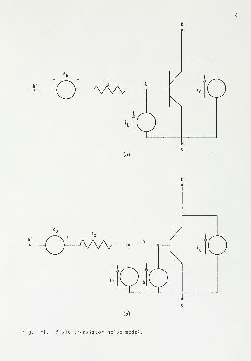
1-1. Basic transistor noise model...... 2
1-2. Hybrid-Pi small signal model of the transistor.... 5
I ~3. Noise model employing the Hybrid~Pi model of the
trans is tor . 6
\~k. Simplified lev; frequency noise model of the transistor.... 8
2~1. Representation of a noisy twoport. 11
2-2. Basic noise measurement system 13
2-3. System for measuring equivalent noise resistance \k
2~k. Simplified low frequency noise model of the transistor.... 16
2-5. Noise model for determination of accuracy of base
res is tance measu rements ,
,
18
2-6. Noise figure versus source res istance for CA -3018-876. 20
2~7. Noise figure versus source resistance for unit Z 21
2 -8. Tetrode transistor structure,.. , .., 23
2_9. Noise resistance versus frequency w i th gate voltage as
a parameter for device ,'/' 195 2k
2~10. Noise figure versus source res istance w ith gate voltageas a parameter for device # 195 25
2_11. Improved low frequency noise model for the 1 /f noise
reg f on ........ 26
2~! 2. Transistor structure showing two components of the
base resistance of a transistor 28
2~13. Noise resistance versus frequency for device it 1^7 31
vi

LIST OF FIGURES (continued)Page
FIGURE
2-14. Noise figure versus source resistance for device
# 147 32
3"1. Burst noise waveforms. 35
3 "2. Burst noise model 37
3*3. Equivalent burst voltage versus source resistance 39
3"4. Random telegraph wave spectrum , 40
3-5. Burst noise spectrum 41
3-6. Two level burst noise spectrum..... 43
3"7. Multi-level burst noise model 44
3"8. Equivalent burst voltage versus temperature w i th
collector current constant 45
3-9. Equivalent burst voltage versus collector currentat constant temperature.... 46
3- 10. Average burst rate versus collector current at
constant temperature 47
3 — 11. Equivalent burst voltage versus temperature withconstant emitter-base voltage 49
3~12. Collector current versus gate voltage shavingpresence of burst noise 50
3-13. Noise model including 1 /f surface noise and burstnoise generators. , 52
3"l4. Structured spectrum predicted by model includingburst noise and 1 /f noise 53
3"15. Noise figure versus frequency showing structuredspectrum. 54
4~1. Transistor differential amplifier and small signalequivalent circuit 56
4- 2. Equivalent noise resistance versus frequency of thedifferential amplifier 58
vi i

LIST OF FIGURES (continued)
Page
FIGURE
h~3. Lav noise amplifier configuration 59
h~k. Small signal model of the low noise amplifier 60
k~S. Theoretical and experimental burst noise reductionusing the low noise amplifier 63
k'S. Noise figure reduction using the low noise amplifier... 64
k~~J . Noise figure versus collector current for low
noise amplifier.,. „ . 65
5"1. Improved lav frequency noise model including two1 /f noise generators and the burst noisegenerator „ „ 67
5~2. Low noise amplifier conf igurat ion. ........... , 69
A~l. Basic noise measurement system... 72
A -2. Actual noise measurement system 73
A -3. Transistor test jig. 76
A -4. Burst noise measurement system 77
A _5. Burst rate measurement system........ 79
A-6. The infinite limiter.. . 80
A~7. Methods of Beta measurement „ 81
A _8. Test jig for h. measurement..... 83J le
A _9. Differential amplifier test jig 8k
A _10. Low noise amplifier 85

Abstract of Dissertation Presented to the Graduate Council
in Partial Fulfillment of the Requirements for the Degree of
Doctor of Philosophy
LOW FREQUENCY NOISE SOURCES IN
BIPOLAR JUNCTION TRANSISTORS
By
Richard Charles Jaeger
June 1969
Chairman: E. R. ChenetteCo-chairman: A. J. BrodersenMajor Department: Electrical Engineering
This dissertation is concerned with the sources of lew frequency
noise in bipolar junction transistors. Noise measurements on silicon
planar diffused transistors indicate that the present noise model
inadequately represents the noise performance of modern transistors.
An improved noise model is presented which includes three distinct
excess noise sources. Two of the noise sources have a 1/f noise
spectrum. One represents noise generated at the surface of the
transistor; the other represents noise generated in the emitter-base
space charge region. The importance of the third source of 1 om
frequency noise, burst noise, has only been recognized recently since
the advent of monolithic integrated circuits. Burst noise consists
of sudden discrete shifts in the dc collector current of the transistor.
The erratic behavior of this noise can severely impair the performance
of high gain integrated amplifiers. The electrical behavior of burst
noise is experimentally investigated and a phenomenol og i cal noise
generator is developed.

A transistor amplifier configuration utilizing two transistors and
a dc current source is analyzed using this improved noise model. Both
the analytical and experimental results shew that this configuration
is capable of dramatically reducing the effects of the low frequency
noise sources of bipolar junction transistors.

CHAPTER ONE
INTRODUCTION
Hi st or ical Backg r ou nd,
Theory of the low frequency noise performance of the bipolar
junction transistor has existed for many years and has remained
essentially unchanged since its inception (1, 2, 3). The essence of
the shot and thermal noise performance of the transistor is shown in
Fig. 1_
1 a. The shot noise of the intrinsic transistor may be repre-
sented by a shot noise generator i, in parallel with the base-
emitter junction and a shot noise generator i in parallel with the
collector-emitter terminals of the transistor. Also shown in Fig. l_ la
is the thermal noise generator e, associated with the extrinsic base
resistance of the device. The lav frequency 1 /f noise of the
transistor may be represented by a flicker noise generator in parallel
with the emitter-base junction of the transistor as developed by
Fonger (k) . The basic lav frequency noise performance of the transistor
is represented in the model of Fig. l
_ lb.
The source of the 1 /f noise represented by the above noise
generator has been a source of considerable conjecture. Fonger
originally associated 1 /f noise with fluctuations in current recanbining
at the base surfaces. More recently Sah (5) and others (6) have shavn
1
A/W
(a)
-AAA/
(w
Fig. 1~1. Basic transistor noise model.

3
more experimental evidence supporting the surface noise theory.
Gibbons (7) has suggested that the source of 1 /f noise in lew noise
transistors is the emi tter"base transition region rather than the sur"
faces of the device. Knott (8) recently concluded that there is 1 /f
noise originating within the transistor. Investigation is clearly
needed to determine whether more than one 1/f noise generator exists
in the transistor and to determine the proper location in a transistor
noise model of the generators which are found to exist.
Another noise phenomenon, burst noise, has been entirely neglected
in the transistor noise model. Originally noticed in carbon resistors
and reverse-biased p~n junctions, burst noise has only recently been
recognized as a problem in transistors (9, 10). With the advent of
integrated circuits, and their associated yield problems, the luxury
of ignoring or disposing of bursting units can no longer be afforded.
One can no longer select special low noise units with which low noise
amplifiers may be constructed, but must accept the performance of the
transistors comprising the integrated amplifier. Thus burst noise
cannot be tolerated in low noise integrated amplifiers. The breadth
of this problem and lack of available information about burst noise
indicate that a study of this phenomenon is needed. This noise form
is neglected in the noise model of Fig. 1~1, and a generator character-
izing the effects of burst noise should be included in any complete low
frequency noise model of the transistor.
Both burst noise and 1/f noise reduce the sensitivity of amplifiers
at low frequencies. The present method of controlling 1/f noise is
to attempt to produce transistors having "clean" surfaces and oxides
by careful process control. At this time there is no known method of
controlling burst noise. Investigation is needed to determine if
circuit techniques exist through which the 1/f and burst noises may
be control 1 ed.
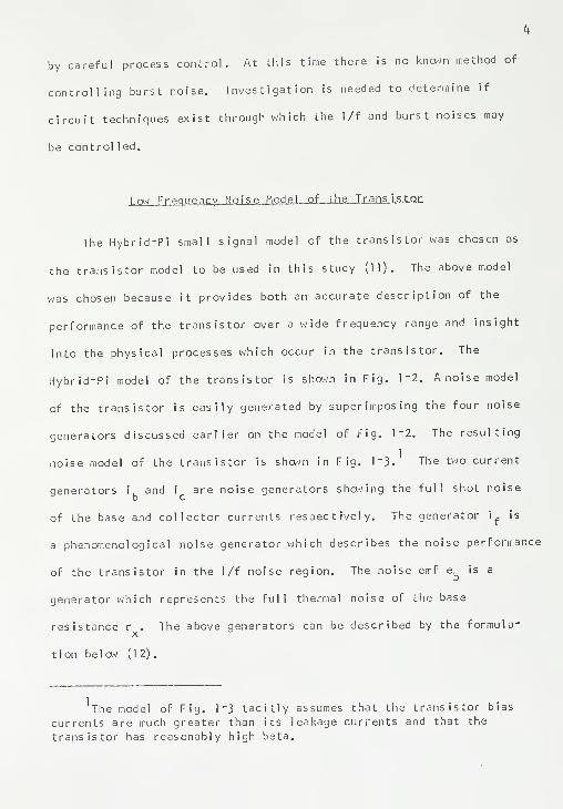
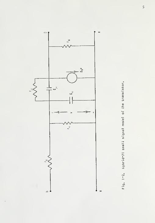
I nrj Frequency Noise Model of the Trans i s tor.
The Hybrid-Pi small signal model of the transistor was chosen as
the transistor model to be used in this study (11). The above model
was chosen because it provides both an accurate description of the
performance of the transistor over a wide frequency range and insight
into the physical processes which occur in the transistor. The
Hybrid-Pi model of the transistor is shown in Fig. 1"2. A noise model
of the transistor is easily generated by superimposing the four noise
gene rators discussed earlier on the model of Fig. 1-2. The resulting
e model of the transistor is shown in Fig. 1~3. The two current
generators i, and i are noise generators shoeing the full shot noiseDCof the base and collector currents respectively. The generator i^ is
a phenomenological noise generator which describes the noise performance
of the transistor in the 1/f noise region. The noise emf e. is a
generator which represents the full thermal noise of the base
resistance r . The above generators can be described by the formula-x
t ion bel ow (12).
The model of Fig. 1 "3 tacitly assumes that the transistor bias
currents are much greater than its leakage currents and that the
transistor has reasonably high beta.

6
-VW^
o
J:
o-33—
I
o

7
2ql rdf (1.1)b ^ C
2 = 2ql Q df (1.2)
^kTr df (1.3)b x
i* = KlBdf/f (1.4)
For low frequencies the model of Fig. 1 "3 may be considerably
simplified. At lew frequencies the effects of C and C are unimport"
ant, and these capacitors may be deleted from the model. The resistor
r affects the gain of the transistor only when the device is operated
under conditions of high voltage gain and may also be neglected.
The result of these simplifications is the model of Fig. 1 ~h. The
model of Fig. 1—
^4 will be the low frequency noise model used throughout
this noise study.
Summary
The purpose of this work as developed above is twofold. First
the 1/f and burst noise phenomenon are to be studied and modeled, and
then methods of controlling these two noise forms are to be invest i~
gated.
Chapter Two presents the results of an experimental study of 1/f
noise beginning with the above low frequency noise model and resulting
in the development of an improved noise model which more fully explains
the noise performance of the transistor in the 1/f noise region.
Chapter Three presents the results of a study of burst noise
including modeling of burst noise by a burst current generator,
determination of the functional dependence of this generator, and
qualitative ideas as to the origin of the burst noise phenomenon.

-<-
+ —aSj-
AAA/

A lew noise amplifier configuration is presented in Chapter Four.
This amplifier should provide a method of realizing lev; frequency low
noise amplifiers whose noise resistance is basically limited by the
thermal noise of the base resistances of the transistors comprising
the amplifier and by the shot noise of the collector current of the
second transistor of the amplifier configuration. This amplifier
also provides a method of effective control of burst noise.
Results of this study and recommendations for further work
indicated by this study are presented in Chapter Five.

CHAPTER TWO
1/f NOISE SOURCES IN BIPOLAR JUNCTION TRANSISTORS
Noise Figure a nd Equivalent Noise Resistance
In any noise study it is necessary to have a noise measure which
may be used to compare the noise performance of various noisy devices.
Two common and convenient measures are equivalent noise resistance Rn
and noise figure F. Equivalent noise resistance and noise figure,
developed below, will be used to characterize the noise performance of
devices throughout this thesis.
The noise of a twoport may be conveniently represented by two
noise sources as shown in Fig. 2- la (13, 1^+). For a given input
termination R , the equivalent circuit of the twoport may be further
reduced to the circuit of Fig. 2~!b in which the noise source e is
given by
et
= e + iRs
. (2.1)
2The total mean square noise voltage e at the input of the twoport
may be computed with the aid of Nyquist's theorem (15),
e2
= e2+ i+kTR df (2.2)
n t s'
and can be represented by the equivalent circuit of Fig. 2"lc in which
R is now a noiseless resistor. The noise emf e may be expressed as ans n
equivalent noise resistance defined by
10

11

12
R = J/tkTdfn n
(2.3)
In this form, the equivalent noise resistance Rn
is a convenient
quantity by which various noisy devices may be compared. Noise figure
F may be defined in terms of the equivalent noise resistance Rn
and is
given by the formula below (16).
F = R /Rn s
(2.4)
Thus equivalent noise resistance R provides both an effective method
of comparing the noise performance of various devices and a method of
determining the corresponding noise figure F.
Measurement of equivalent noise resistance R can be accomplished
using a sinusoidal comparison technique (17). Figure 2~2 shows the basic
measuring system consisting of the device under test, a sinusoidal
calibrating signal, a noiseless variable gain amplifier, a filter, and
a quadratic detector.
The device under test may be represented by an equivalent noise
resistance followed by a noiseless twoport having a gain A as shown in
Fig. 2~3. The equivalent noise resistance R may be determined using the
following procedure. With the switch in position one, the reading Ml of
the detector will be
Ml = (4kTR df),/2
Al • AVI (2.5)
With the switch in position two and with the amplifier gain set to the
second gain setting, the detector reading M2 is obtained.
M2 = (e ,
2+ 4kTR df)
1/2• Al • AV 2
cal n(2.6)
Ch oosing the calibrating signal such that M„ = M .:
(e ,
2+ %TR df)Al
2AV2
2/(4kTR df)Al
2AVl
2= 1. (2.7)
cal n n i
This may be easily solved for noise resistance R yielding
R = e2
, /(JfkTdf) (AV1/AV2)2(1"(AV2/AV1)
2) .
n cal!2.3)

CXZ C3 Q-
13
LtJ CtlUJera co
C.3 LlJ I
—

CC CO Q-
14
-a

15
The value of noise resistance R is determined using the aboven
equat ion.
Lav Frequency Noise Performance of the Transistoras Predicted by the Ex ist ing Noise Model
The lav frequency noise model of Chapter One is shown in Fig. 2~k.
The noise figure of the transistor obtained from this model is
F = 1 + r /R + g (R +r )
2/2h rc R + g (R +r +g /g )
2/2R r
2
x s m s x FE s m s x M o m s p o
+ TJ(R +r )
2/4kTR df
f S X s(2.9)
The above expression may be simplified by considering two noise
regions; a region in which the 1/f noise generator dominates the
transistor noise performance, and a region in which shot and thermal
noise generators are dominant. The resulting expression for noise figure
in the shot noise region is
F = 1 + r /R + g(R +r )
2/2h CI_R + g (R +r +6 /g )
2/2R R
2.
x s m s x FE s m s x o m s o
(2.10)
This expression for the noise figure in the shot noise region has a
minimum value F . qiven below (18).mm 3
Fm in
=] + 9m (VRS
min)/h
FE(2J1 )
RSmin
= [(hFE
(1 + 2Vx + (Vx'Xe''^^ ^*The noise figure of the transistor may be minimized by the proper
selection of source resistance R . For a given value of r , the noises x
figure may be computed in the shot noise region, and the model of
Fig. 2~k may be verified for the shot noise region.
In the 1/f noise region the 1/f noise generator dominates the noise
performance, and the noise figure expression of Eqn. 2.S reduces to the
express ion

AA/V
16
+ —*s$-
A/W
—3-

17
F = 1 + i ?(R +r ) VlkTR df . (2.13)f X X s
This expression may also be minimized by proper choice of source
res istance R .
F . = 1 + i?(r /kTdf) for (2. 14)mm f x
R . = r (2.15)sm i n x
Noise figure measurements in the 1 /f noise region may thus be used to
determine the value of the base resistance r of the model of Fig. 2~h.
The noise figure in the 1 /f noise region must be of a sufficient
magnitude to insure accuracy of the measurements of r using the above
method. The sufficient magnitude is determined below. For the model
of Fig. 2_5, the noise figure is easily determined to be
?~~7 gm
F = 1 + r /R + M(R +r ) /R , M = i^AkTdf + "T?
—
x s s x s f 2h
(2.16)
which has a minimum for
R . = (r2
+ r /M)1/2
. (2.17)smin x x
Manipulation yields
r2
= R2/ [1 + k? . /(F . -I)
2] (2.18)
x s mm mmThus for r to be determined within one percent. F . in the 1/f noise
x mmregion must be at least 202. A minimum noise figure of 20 is required
if r is to be determined within ten percent.x
Measurements of noise figure versus source resistance in the 1/f
noise region can be used to help characterize the model of Fig. 2~k.
The base resistance r may be easily determined by noise measurement in
the 1/f noise region. Then, knowing r , the minimum noise figure and
source resistance corresponding to this minimum may be calculated for
the shot noise region. Measurements in the shot noise region may then
be used to check the validity of the noise model of Fig. Z~k.

Fig. 2-5. Noise model for determination of accuracy of base resistancemeasurements.

19
The apparent validity of the preceding noise theory is demonstrated
by unit CA-3013-876. Measurements of noise figure versus source
resistance in the 1/f noise region yield a value of r = 560 ohms as
indicated in Fiq. 2~6, Measurements of F versus R in the shot noise3s
reqion yield values of F . and R . of 1 . 26 and 5 kohms respectively,mm sm in
also shown in Fig. 2-6. Values of R . and F . , 5.6 kohms and 1.24sunn min
respectively, predicted using Eqns. 2.11 and 2.12 with the above
values of r .show excellent agreement with the above measurements. Smallx' D
signal measurements yield a value of r = 5^5 ohms. Thus the noise
model of Fig. 2~h correctly predicts the low frequency noise performance
of the transistor tested, and the 1/f noise generator sees the same
base resistance as the base current shot noise generator.
Breakdown of t he Existing N oise Mod el
The transistor discussed above demonstrated very good agreement
with the accepted noise model and its theory. However, 1 cw frequency
noise measurements upon other transistors have shown little agreement
with the above theory. The 1/f noise generator above sees the total
base resistance r , and the minimum noise figure in the 1/f noise
region should occur for a source resistance R equal to the base
resistance r . In most cases, as shown by the typical unit of Fig. 2~7»
the value of r obtained by small signal measurements disagrees greatly
with that obtained from noise measurements in the 1/f noise region.
Unit Z has a base resistance value of 7-8 kohms determined by small
signal measurements, but the indicated value of r determined from' x
Fig. 2-/ is 2.7 kohms.

20
1000
300-
100-
30
0—
3—
UNIT CA-301 8-876
l
c- 100,ua
5000 HZ
100 300 Ik 3k
SOURCE RESISTANCE (ohms)
10k 30k
Fig. 2~6. Noise figure versus source resistance for CA-301 8-876.

21
10
6—
2 —
UNIT Z
l
c= 500/ja
F - 45HZ
2000 4000 6000
SOURCE RESISTANCE
1000
Fig. 2"7. Noise figure versus source resistance for unit Z.

22
The origin of this discrepancy was studied further by producing special
four terminal devices, tetrode transistors, in the Microelectronics
Laboratory of the University of Florida. The geometry of the tetrodes is
shewn in Fig. 2-3. The fourth electrode consists of a field plate or
gate physically located over the emitter-base junction of the transistor.
By applying a potential to the gate the carrier densities at the surface
of the transistor under the gate can be altered, and any mobile ions in
the oxide under the gate may be affected. It is also known that a
potential on this gate will affect the 1 /f surface noise of the device
(19, 20).
Measurements of noise figure versus frequency for device // 1 95 are
shown in Fig. IS. As the gate voltage is increased, the 1 /f noise of
the device increases greatly as expected. Measurements of noise figure
versus source resistance for device #195 are shown in Fig. 2-10. The
value of R of these figures varies widely as the gate potential andsmin
hence 1 /f surface noise varies. The variations above may be accounted
for through the model developed below.
fl n Impr^'H N <->ise Model Including Tw o 1 /f NoJs^_S^nexa_Loxs.
Consider the noise model of Fig. 2"11 in which two 1 /f noise
generators are shown. The noise figure in the 1 /f noise region is found
to be
F = 1 + l?.(R +r )
2AkTR df + xl (R +r ) VfkTR df . (2.19)
t~ I S 3 S T c. S X *
Again the expression for noise figure may be minimized through the
proper choice of R .
2 2^ ,„ .v ,1/2 __ .2 ..2
R . = [(r* + erV(l +0]' /Z,
e= it /it . (2.20)smin a x rzri

23
1I
T
EMITTER
CONTACT OPENINGS
Fig. 2~8. Tetrode transistor structure.

2k
5 —
2 —
2 —
1C:
UNIT #195
l
c= 100/ja
Rs
= 510fi
20 50 200 500
FREQUENCY (HZ)
1000 2000 5000
Fig. 2-9. Noise resistance versus frequency with gate voltage as a
parameter for device //' 195.

25
.- 0)
O E
3U(19IJ 3SI0N

A/W
26
AA/V
AAAr

27
Two cases of Eqn. 2.19 emerge, depend ing upon the dominance of
either i.. or i as shown below.
For i,.. sufficiently large,
R . = r and F . = I + i?,r /kTdf . (2.21)smin a mm fl a
For i r „suf
f
icien tl y larqe,f2
R . = r and F . = 1 + i? r /kTdf .. (2.22)sin in x mm f 2 x
As the ratio of the two noise sources, £ , varies, R . variessm i n
between the values r and r . The values of r and r may be deter"ax x a
mined as discussed below.
Earlier measurements have confirmed the validity of the model of
Fig. 2~k for some transistors. In that model it was seen that the 1 /f
noise generator and the shot noise generator shared the same position
in the model. This generator should then be associated with the active
base region of the device. As discussed in Chapter One, the existence of
a generator in this location has been alluded to in the past. Other
measurements have associated 1 /f noise with the transistor surfaces,
particularly near the surface of the emitter-base junction. The
approximate position of the above generators can be determined from the
device geometry as shown in Fig. 2"1 2. The total base resistance r
of a transistor may be divided into two parts; a portion due to the
inactive base region between the base contacts and the edges of the
emitter and a portion corresponding to the active base region under the
emitter of the transistor as sho.vn in Fig. 2-12 (21). A noise generator
associated with the surface of the emitter-base junction should see only
a portion of the base resistance corresponding to the inactive base
region rather than the total base resistance of the device. On the other

28
\SE CONTACT BASE CONTACT-
V//A
29
hand a noise generator associated with the active base region would see
the total base resistance of the device.
The base resistances of Fig. 2"1 1 can now be determined. The
resistance r is approximately the base resistance due to the inactive
base reqion, and the sum r + r, is equivalent to the total base3' a b
resistance of the device so that
rx
= ra
, rb
. (2.23)
Measurements upon device //195 determine the values of r and r,
of the model of Fig. 2.— 11. The geonetry of the tetrode transistor
indicates that there is 1/18 square of material in the inactive base
region. Sheet resistivity measurements for device //195 yield a value
of 1 80 ohms per square for this region and hence a value of ID ohms
for the value of r . Small signal input impedance measurements indicate
a value of 650 ohms for the total base resistance r yielding a value
of 630 ohms for r, . The measurements given in Fig. 2-10 clearly show
values of R . which fall within the range of 20~650 ohms. Thissniin
performance is predicted by the model of Fig. 2"! 1 and the ratio e of
Eqn. 2.20 is effectively varied by varying the value of the gate
potential on the tetrode.
Separate Dominance of th e Two 1 /f Nois e Gen erators
The noise figure in the 1/f noise region for the improved noise
model of Fig. 2~1 ] was given in Eqn. 2.19. If the noise generator ip„
is sufficiently dominant, the noise figure would be given by Eqn. 2.22.
This was the case of the CA-3OI8 of Fig. 2"6. The case of dominance of
the generator if
. was developed in Eqn. 2.21, and is demonstrated below.

30
Device #1^7 was a specially treated device in which 1/f surFace
noise could be made the dominant noise Form. Before metal izat ion the
oxide over the surFace of the above transistor was contaminated with
sodium ions by heating the transistor in a saturated salt solution at
95 C for twenty minutes. This treatment introduces mobile sodium ions
into the oxide which may be later influenced by the potential on the
gate electrode (22, 23). The completed transistor was subjected to heat
treatment at a temperature oF 200°C For FiFteen minutes with the gate
biased at First to plus fifty volts and then later at minus fifty volts
with respect to the other electrodes. The heat treatment with the gate
positive causes the mobile ions to drift toward the silicon-silicon
dioxide interface, and with the gate negative the ions drift toward
the gate electrode. The results of noise measurements upon the transistor
with the ions drifted both toward and away From the transistor surFace
are shown in Fig. 2-1 3. With the ions drifted toward the gate electrode
a structured spectrum was obtained. This will be discussed later. V/ith
the ions drifted toward the surface of the transistor, 1/f noise enhanced
the noise spectrum by almost 20 db. Since the 1/F noise here was
greatly influenced by the ions in the oxide under the gate the dominant
source oF this 1/F noise is the surfaces near the base-emitter junction
oF the transistor. Measurements oF noise Figure versus source resistance
with the ions drifted toward the transistor surFace are given in Fig. 2-1**,
and the indicated value of r of the model oF Fig. 2~9 is 22 ohms. Sheet
resistivity measurements yield a value oF 10 ohms for the bulk material
oF the inactive base region For this device.
The above measurements show the existence of the two 1/f noise
generators of Fig. 2-10 in which ra
is the resistance of the inactive

31
iO _
B —
UNIT #147
Rs
= 3kQ
HEAT TREATMENT
5 MINUTES AT 200°C AND
V„ = +4oV
° - V„ = -40V
103
FREQUENCY (HZ)
Fig. 2_
1 3 . Noise resistance versus frequency for device />' 1^7.

32
31MDIJ 3SI0ii

33
base region, and the total base resistance of the transistor is given
by
r - r + r,x a b
(2.24)

CHAPTER THREE
BURST NOISE
I ntroduct ion
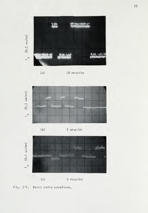
Typical burst noise waveforms are shewn in Fig. 3~1. The waveforms
shown are of collector current versus time and consist of sudden discrete
shifts in the dc collector current of the transistor. The above
phenomenon has long been observed in resistors and reverse-biased p~n
junctions, and recently burst noise has been observed in the transistor.
Burst noise has become a major problem in transistors only
recently. In the past, one could select acceptable quiet devices
with which la-; noise amplifiers could be constructed. In today's
integrated circuit technology this procedure is no longer economically
feasible, and burst noise has become a problem causing reduction of the
yield of acceptable functioning integrated circuits.
The results of a study of the burst noise phenomenon are presented
bel ow.
Burst N oise Mod el and Spec tral Representation
Burst noise has been shown to be a function of temperature collector
current, and source res is tance, and to be independent of collector-base
voltage {2h, 25). The bursts are associated with the base~emitter
Ik
35
(a) 50 msec/cm
-1—1 1 1
M H
36
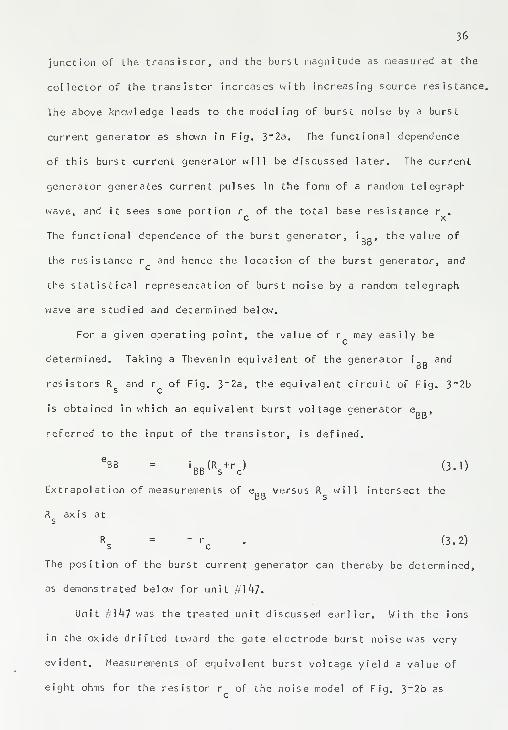
junction of the transistor, and the burst magnitude as measured at the
collector of the transistor increases with increasing source resistance.
The above knowledge leads to the modeling of burst noise by a burst
current generator as shown in Fig. 3"2a. The functional dependence
of this burst current generator will be discussed later. The current
generator generates current pulses in the form of a random telegraph
wave, and it sees sane portion r of the total base resistance r .v c x
The functional dependence of the burst generator, i DD ,the value of
BB
the resistance r and hence the location of the burst generator, andc 3
'
the statistical representation of burst noise by a random telegraph
wave are studied and determined below.
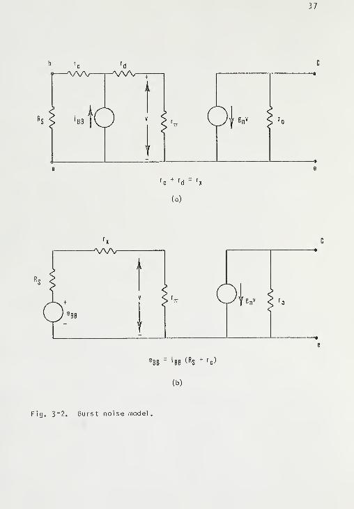
For a given operating point, the value of r may easily be
determined. Taking a Thevenin equivalent of the generator i no and
resistors R and r of Fig. 3"2a, the equivalent circuit of Fig. 3~2b
is obtained in which an equivalent burst voltage generator eDD ,BB
referred to the input of the transistor, is defined.
6BB = i
BB(R
s+r
c>(3.0
Extrapolation of measurements of eDO versus R will intersect theBB s
R axis ats
Rs
- (3.2)
The position of the burst current generator can thereby be determined,
as demonstrated below for unit U\h~l
.
Unit /- 147 was the treated unit discussed earlier. With the ions
in the oxide drifted toward the gate electrode burst noise was very
evident. Measurements of equivalent burst voltage yield a value of
eight ohms for the resistor r of the noise model of Fig. 3~2b as
37
b rc
rd
f WV rAAAr
RS S 'BE 6
rc
+ rd
=rx
AMr
v C r„
eBB
='BB ^ R
S+ r
c)
(b)
Fig. 3"2. Burst noise model.

38
demonstrated in Fig. 3~3. As discussed earlier, the 1/f surface noise
generator of this transistor saw a base resistance of approximately
22 ohms. Thus, within experimental error, both the burst noise and
surface 1/f noise generators are located in approximately the same
region near the surface of the emitter-base junction, and these two
noise generators see approximately the same portion of the total base
resistance of the device.
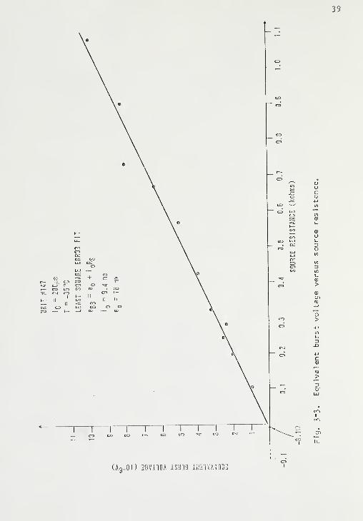
As mentioned earlier, burst noise may be modeled by a random
telegraph wave as discussed below. Since the measuring apparatus removes
the average value of the noise, the burst noise may be conveniently
modeled by a random telegraph wave whose normalized power spectrum is
given by
S(w) = 1/(1 + (TTf/2a)2
) , (3.3)
in which a is the average number of bursts per second (26). The above
paver spectrum is shown in Fig. 3"^, and it has a value of one-half for
w = 2a/ tt. The power spectrum of burst noise may be measured, and the
results correlated with measurements of the average burst rate in
order to confirm the supposition that burst noise can be represented
by a random telegraph wave.
Verification of the random telegraph character of burst noise is
demonstrated by device CA-301 8-1^-5^3. The low frequency noise of this
device was dominated by burst noise, and the average burst rate was
determined to be 369 bursts per second. The normalized noise spectrum
of the burst noise should have a value of one - half for a frequency of
238 Hz. The measured power spectrum of the burst noise is presented in
Fig. 3-5 and has the predicted shape and a half power frequency of
39
— en
L -.
(A3_oi) aovnon lsuna limvAino]
ko
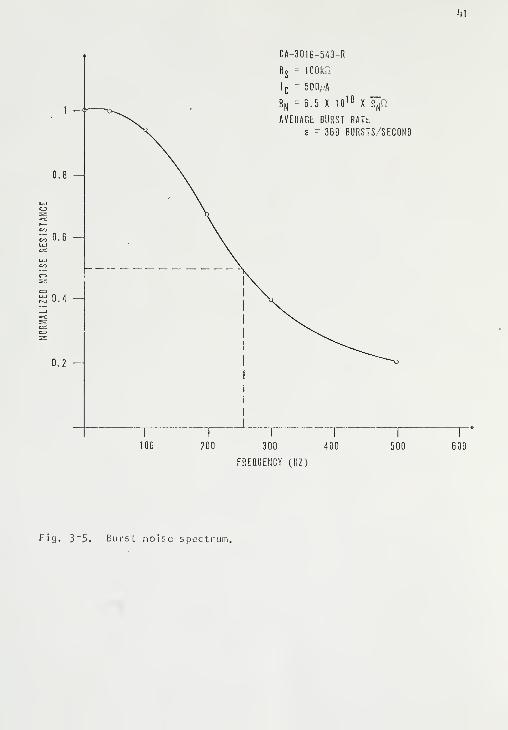
Ill
CA-3018-543-R
OOkO
= 500/./A
= 6.5 X 10,u
X fyn
AVERAGE BURST RATE
a - 369 BURSTS/SECOND
FREQUENCY (HZ)
Fig. 3~5. Burst noise spectrum.

k2
255 Hz, well within experimental accuracy. Burst noise is well
represented by a random telegraph wave.
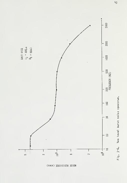
Burst noise may also have multiple levels as depicted in Fig. 3"la.
For a device in which two levels of burst noise are present, the power
spectrum should show the presence of both levels. Figure 3~6 shows
the power spectrum of device #123 which had two dominant burst levels.
The spectrum is the superposition of two burst noise spectra of Fig. 3~k.
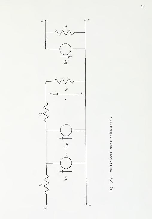
Multiple level burst noise may be modeled as shown in Fig. 3-7 in
which there is a burst noise generator for each burst level.
Funct ional Dependence of Burst Noise
Experimental measurements have been made to characterize the
functional dependence of burst noise. Equivalent input burst voltage
e is found to have the functional dependence given below.
1. e is independent of collector-base vol tage when thetransistor is in the forward active operating region;
2. Fig. 3-8 shows the variation of e as a function oftemperature with I constant. The functional depen-dence is found to Be
il.h)
(3.5)
eBB
= kl
ex P ('T/T
o) ;
3. With temperature constant, equivalent burst voltage is
related to collector current by
eBB
= k2
(lc
)
n. n * 1/2
as indicated in Fig. 3~9.
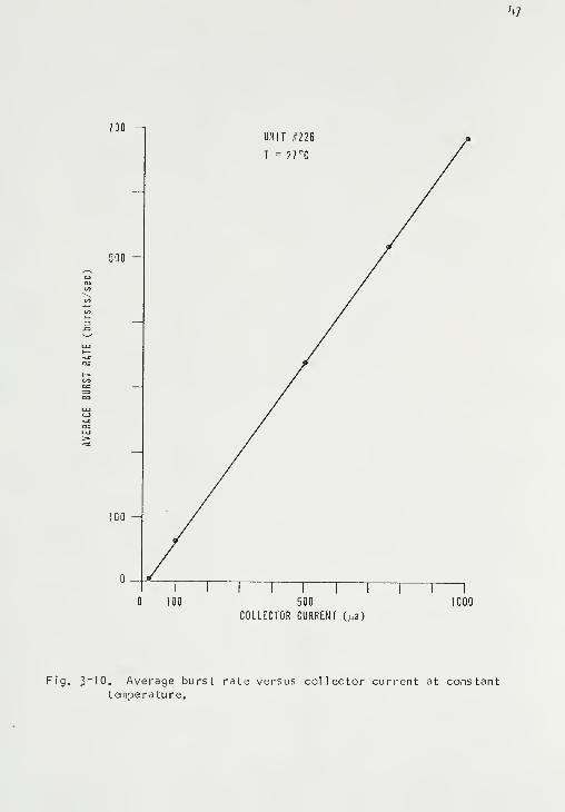
h. Fig. 3-10 demonstrates that the average burst rateis linearly dependent upon collector current whenthe temperature is constant.
ABR = k3
l
c (3.6)
Combining Eqns. 3.^ and 3.5, the overall functional dependence of
equivalent burst voltage upon temperature, collector current, and base-
emitter voltage is determined (27).
hi
(smijo) 30HV1SIS3U 3SI0N
kh
AA/V

hb
10
5 —
2
10-3_
5 —
2 —
10
#89
Rs
= 50kfi
'c
En«r"
26°K
T/T r
-60 -40 -20 20 40 60
TEMPERATURE (
PC)
Fig. 3"8. Equivalent burst voltage versus temperature w ith
collector current constant.

IT #89
kG
100 400 900
COLLECTOR CURRENT (pa)
16UI
30
20
10 -
[IT #126
i |— ~ r100 400 900
COLLECTOR CURRENT (//a)
Fig. 3_9. Equivalent burst voltage versus collector current atconstant temperature.
hi
700 -i
i i r500
COLLECTOR CURRENT (,^a)
1000
Fig. 3"10. Average burst rate versus collector current at constanttemperature.

k8
eBB
= V3/2eXp( "(E "qV
be)/2kT) ex P("T/T )
for n = 1/2 (3 ' 7)
The above expression may be verified by measuring the dependence of
e upon temperature w i th base-emitter voltage constant. The expected8B
variation of Eqn. 3.7 on a normalized basis is shown in Fig. 3"Ha
for typical values of T and E , as determined by computer analysis.
Measured results are given in Fig. 3~llb showing good agreement with
Eqn. 2.27.
Further study of burst noise was undertaken using the tetrode
transistors discussed earlier. By varying the gate potential the
carrier concentrations under the gate may be changed. As the gate
potential is made more positive the base region near the surface of
an npn transistor becomes more and more depleted of majority carriers.
This is evidenced by a fall off in the collector current of the
device (28). The units described by Fig. 3"12 had no evident burst
noise until the base region of the device was sufficiently depleted.
After the appearance of the burst noise, the bursts remained essentially
unchanged until the surface of the base region began to invert, and
then the bursts generally disappeared at this time. Burst noise
appears to be intimately associated with depletion of the base region
near the base-emitter junction.
Drift experiments also indicate a relationship between surface
conditions and burst noise. An untreated device, unit #91, showed
no bursting with the ions in the oxide drifted toward the gate. With
the ions drifted to the surface, burst noise appeared. The burst
noise again disappeared upon drifting the ions back to the gate.

^9
20-
10-
COMPUTED FROM EQN. 3.7
Eg = 1.1 ev. T = 30rK, K
4= 10
« Vpr - JOV'BE
VBE
= .65V
t i i i n i r-30 -20 -10 10 20 30
TEMPERATURE (°C)
(a]
10 -
2-
MEASURED UNIT #22
-30 -20 -10 10 20 30
TEMPERATURE (
CC)
(b)
Fig. 3~11. Equivalent burst voltage versus temperature w i th constantemitter-base voltage.

50
ooo -i
3 500
200
100
ooo 4
500 -
200-
100
1000 ->-
500-
200 -
100
30
BURSTINGj-< — >_
—
,
,
!_
30 60 90
GATE VOLTAGE (volts)
60
20
IT C
BURSTINGh«3 js»-|
30 60 90
GATE VOLTAGE (volts)
120
90 120
GATE VOLTAGE (volts)
150
Fig. 3"12. Collector current versus gate voltage shaving presence ofburst noise.
51
Horn bij : ral Effects of Bu rst and 1 /f Noise
A model of transistor noise including a burst generator and a 1/f
noise generator may be used to further explain observed noise spectra.
Using the model of Fig. 3"13, the noise figure may be computed to be
F = 1 + k.f /f + k./(l + (7rf/2a)2) . (3.8)
I c L
For the proper relationship between constants k. and k , the noise
figure spectrum of Fig. 3"1^ may be obtained. The burst and 1/f noise
regions are clearly defined. The above effect is demonstrated in
the spectrum presented in Fig. 3~15. The spectrum of device 2N930"5^
shews first a burst noise character and then a 1/f noise character as
frequency is decreased. Many transistors show the presence of signifi"
cant components of both 1/f noise and burst noise, and the spectrum of
Fig. 2- 28 can often occur.

" t
b^
-AAA^
-\—<j-
AAAr

53

3. G
5k
3M1DU 3SI0N

CHAPTER FOUR
LOW NOISE AMPLIFIERS
Any noise source associated with an amplifier may reduce the
sensitivity of that amplifier. At low frequencies, burst noise and
1 /f noise are most significant in reducing the sensitivity of an
amplifier. Methods of controlling burst and 1 /f noise are discussed
below, and a new low noise amplifier is proposed.
Because of the proximity of devices in integrated circuits,
thermal coupling between devices has been postulated as a possible
source of correlation of the 1/f noise sources in adjacent transistors
in integrated circuits (29). The differential amplifier of Fig. h~]a
is ideal for studying the possible correlation of 1/f noise sources
in devices. Using the small signal equivalent circuit of Fig. k~]b,
the differential output noise is found to be
Vd
2
o = (6oRLR
's/(R
s+r,))
2( i
fl+ '« ' W7l ' WW '
(4.1)
Positive correlation could improve the noise performance of the
transistor differential amplifier. If no correlation is present,
other amplifier configurations must be studied in order to find a
method of controlling noise.
55

56
WW—I
—
(\-H

57
Fig. h~2 shows the noise spectra of two matched transistors of
the transistor array CA~3018 _G. The lower spectral curves are of
transistors 3^5 and 678 of the above array operated separately in the
common emitter connection. The upper spectrum is of the same
transistors operated in the differential amplifier configuration.
Close examination shows that the upper curve is the sum of the lower
two, indicating that the noise of the two transistors in the
differential amplifier adds quadrat ical1y. Thus no correlation is
present in these transistors throughout the spectrum measured.
The transistor amplifier of Fig. k~3 provides an amplifier
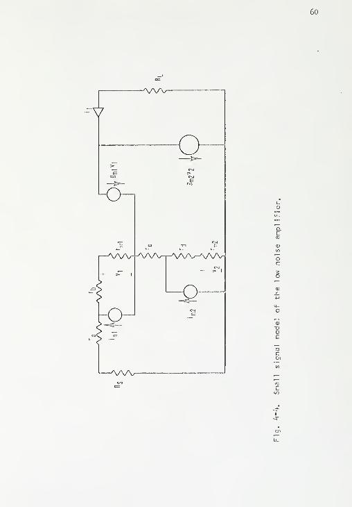
in which 1/f, bursty and shot noise can be controlled. The small signal
model of Fig. k~k is used to analyze the noise performance of this
stage. The generators i , and i ,. can represent either 1/f, shot,33 nl n2 r '
or burst noise generators depending upon the choice of the base
resistors r , r. , r , and r ,. The components of load current causeda bed '
by the noise generators i . and i „ are given below.'
Dnl n2 3
i./i . = 3 (R +r +r +r +3 (R +r )-r.-r ,)1 n 1 os a tt2 x2 o
v
s ay
b v]'
R + ri+ «*^, +(3 +1) (r „+r J
S Xl T] O x2 7T2
i,/i , = 3 ( (3 +l)r -R -r , +r n +r, - r .)1 n 2 o o c s xl tt2 d ttT
R + r . + r . + (3 +1) (r _ + r )s xl irl o x2 Til'
For the proper choice of the collector current ratio
I ./ I = r „ / r . for 3 constant {k.k)cl c2 tt2 7t| o
the load current component caused by i . or i „ may be set to zero.nl n2
i, / i , = for1 nl
l
c2/ l
c]= l + ((3
o+l) (R
s+ra
) -rb+ ra)/ r7T2 (4.5)
(h. 2)
(4.3)

58
(swijo) 30NV1SIS3H 3SIOB

AA/V59
AA/V
60
AAAr
-v
O
rAA/V-A/W
4 > I
-.a
-a
-:t-

i, / i , = For1 n2
I J I , = 1 + 3 r /r _ -(R +r ,-r J/r , (4.6)c2 cl octt2 sxlx2 t2
The current source of Fig. 4~3 may be adjusted for the desired collector
current ratio required to remove the desired noise component from the
output current of the amplifier. This technique may be used to
remove burst noise, 1/f noise, and shot noise components of load
current. The noise resistance of this amplifier is then basically
limited by the thermal noise of the base resistances r . and r „ plus' xl x2
the shot noise of the collector current I „ since the noise of thesec2
generators cannot be affected in this configuration. The voltage
gain of the configuration of Fig. 4~3 is found to be
A = 3 (3 +2)R./(R + r . + r . + (3 +1) (r ,+r .)) (4.7)V o o 1 S X 1 IT 1 O X 2 Tt 2'
which is approximately equivalent to that of a common emitter amplifier
stage operating with a small source resistance. Analysis of the
frequency response of the amplifier of Fig. 4"3 finds that it is
comparable to that of the common emitter stage also as shewn in Table k~\
TABLE k-\
GAIN AMD BANDWIDTH OF THE LOW NOISE AMPLIFIER
R - .01 R = .1s s
Gain Bandwidth Gain Bandwidth
C-E 189 .406 161 .127
Multiple Transistor9 g ^ g8 2
Ampl i f ier

62
The amplifier of Fig. 4- 3 can provide excellent noise performance at
low frequencies in trade for a loss of gain without sacrificing band-
width performance as compared to a common emitter stage operating under
equivalent conditions.
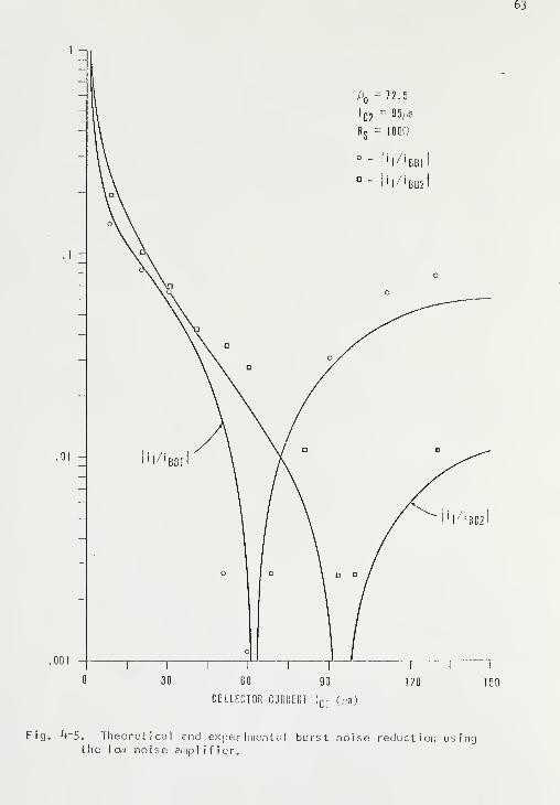
The use of the amplifier to control burst noise is demonstrated
in Fig. k~5. The theoretical and measured curves of burst noise load
current versus collector current I , are shewn in this figure for thecl
3
cases in which transistor T. is bursting and then in which T„ is
bursting. The results shew that the burst noise may be eliminated by
proper selection of the collector current I ..cl
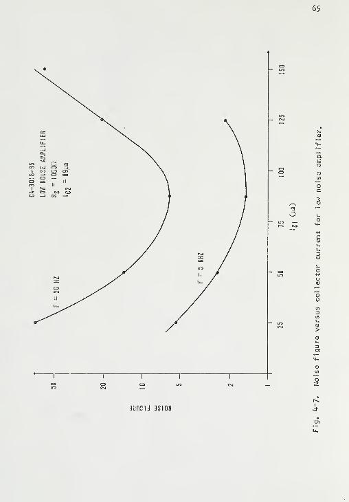
The same amplifier configuration should provide effective control
of 1 /f and shot noise also. Dramatic evidence of this is presented
in Fig. h~ 6. The noise spectrum of the amplifier is shown for various
values of collector current I ,. By adjustinq I . for a noise minimum,cl '
Jcl
a reduction of noise figure from 10^+0 to 6 is obtained at a frequency
of 20 Hz. The breadth of this null is shown in Fig. h~2> indicating
that adjustment of I . is not extremely critical. The results above
indicate that the transistor amplifier of Fig. k~~] may be used to
produce very low noise amplifiers for low frequencies through proper
amplifier adjustment and transistor matching and selection.
63
.0]
f3 =72.5
Iq2 = 95/^a
60 90
COLLECTOR CURRENT l
c ,
(/a)
120 150
Fig. k~5. Theoretical and experimental burst noise reductithe lav noise amplifier.
on us i ng

Gk
2000 —
000—
500 —
200
2r 100-
^ 50
20
10-
5-
2-
20 50 II 200 500
FREQUENCY (HZ)
000 2000 5000
Fig. k~6. Noise figure reduction using the 1 ow noise amplifier.
65
3111)3 1 J 3SI0N
CHAPTER FIVE
CONCLUSIONS AND RECOMMENDATIONS
The preceding work has produced several results which are
discussed below.
1. Burst noise has been studied and the phenomenon characterized.
Burst noise in bipolar junction transistors has been shown to be
associated predominantly w ith the base-emitter junction and with the
depletion of the surface of the base region near this junction.
2. The existence of two 1/f noise generators has been demonstrated.
One noise generator has been shown to be associated with the surface
noise of the emitter-base junction of the transistor. The second 1/f
noise generator is associated with the active base region of the
transistor. Trie presence of the second 1/f noise generator as
speculated by Gibbons has been shewn to exist.
3. An improved model of the low frequency noise of the bipolar
junction transistor has been developed and is illustrated in Fig. 5~1
.
The model includes the shot and thermal noise generators plus two 1/f
noise generators and the burst noise generator discussed above. The
sum of the resistances ra
and rb
of the model of Fig. 5~1 represents
the total base resistance of the. transistor in question, and the
resistor rg
is the resistance of the material of the inactive base
region of the transistor.
66

67
-OW'vw-
0!0EmV
j—
»
e
rx
=ra
+ rb
\i = 2qLdf
•f = 2qlBdf
V =4kTfxdf
i
BB2 = K
3df/[1 + (77f/2a)
2]
i
{ ,
2-[K,l
B
7,tif]/f
71
i
f22 =[K
2l
B
72tif]/f
a2
Fig. 5~1. Improved lew frequency noise model including two
1/f noise generators and the burst noise generator.

68
k. A lav frequency lav noise amplifier configuration has been
demonstrated. Effective control of burst noise is possible through the
use of the amplifier of Fig. 5~2. The same amplifier configuration
can be used to realize amplifiers having very low equivalent noise
resistances at lav frequencies. The noise resistance of the above
amplifier is basically limited by only the base resistances of the
transistors used to build the amplifier and by the shot noise of the
collector current of the transistor T~ of Fig. 5~2.
5. The improved noise model has been used to predict and explain
the existence of structuring of noise spectra which have been observed
but have remained unexplained until this time.
Several areas which deserve further study have originated as a
result of this research and are discussed below.
1. The preceding work has demonstrated the existence of a
1 /f noise source associated with the active base region of bipolar
junction transistors. The origin of this 1/f noise source needs to
be determined.
2. Further study of burst noise is indicated. The physical
cause of burst noise deserves investigation with the hope that this
will lead to methods of process oriented control of the burst noise
phenomenon.
3. The lo/v noise amplifier developed in Chapter Four deserves
further study. The possibility of realizing a very lav noise amplifier
at low frequencies is most stimulating. The configuration appears to
be amenable to integration, and in fact much of its performance is due
to the matching which can be obtained between devices in integrated

69
A/W
A/W

70
circuits. It is recommended that this amplifier configuration be
exhaustively studied.

APPENDIX
MEASUREMENT SYSTEMS AND METHODS
The results of Chapters Two, Three, and Four were obtained using
the systems described in this Appendix. Two major systems are
described which can be used to determine noise resistance, noise
figure, and equivalent burst noise voltage. Other minor systems are
described, and methods of measuring transistor parameters developed.
The system used to measure noise res i stance was described in Chapter Two.
The block diagram of this system is shewn in Fig. A~l
.
The actual measurement system is shewn in Fig. A _2. A Hewlett"
Packard HP~Wtl oscilloscope is used as the system's variable gain
ampl if ier and to monitor the noise output of the device under test.
Following this amplifier is a monitor osc i 1 1 oscope which is used to
insure that no clipping of the noise occurs in the main amplifier.
The filter and quadratic detector are contained in a Quan-Tech wave
analyzer. This wave analyzer tunes from 1 Hz to 5 kHz with bandwidths
of 1 Hz, 10 Hz, and 100 Hz with a full scale sensitivity of 30 V to 100
v o! ts rms. The wave analyzer permits the selection of four meter time
constants of 0.1, 1, lO^nd 100 seconds, providing excellent averaging
capability. A dc analog recorder output drives a chart recorder which
is used to provide accurate determination of a given meter level. The
calibration signal is derived from the BF0 output of the wave analyzer
71

CC CO o3 UJ
72
CC C3 Q.
L.

73

Ih
and is set to one volt rms. This signal is monitored on a voltmeter
and oscilloscope, and it is fol laved by variable attenuation to provide
an adjustable calibrating signal.
Use of the system is as fol lavs. V/ith the calibrating switch open,
the noise in a particular frequency range is measured with a given
amplifier gain setting, and the detector reading is recorded. The main
amplifier gain is then reduced by an arbitrary factor (100 times for
example). The calibrating signal is introduced by closing the
calibrating switch, and the attenuator is adjusted until the original
detector level is attained as monitored on the recorder. The equivalent
noise resistance is then given by:
R = l/[ (h(AV2/AVl)2)(^kTdf) (ant i 1 og (total systan
attenuation in db/10))] . (A.l)
In the above expression, AV1/AV2 is the ratio of the main amplifier gain
settings, and the total system attenuation also incorporates this
figure. An accurate knowledge of the effective noise bandwidth df is
necessary to provide accurate measurement of noise resistance using the
above system. The filter characteristics of the wave analyzer were
experimentally measured, and the effective noise bandwidth was deter"
mined by numerical integration. The results of this process yielded
effective noise bandwidths of 1.23Hz, 12.5 Hz, and 125 Hz, for the I Hz,
10 Hz, and 100 Hz bandwidth settings of the wave analyzer respectively.
Also affecting the accuracy of the system is the background noise of the
main amplifier and wave analyzer. Therefore, continual checks must be
made in order to insure that the background noise of the system is
negl igible with respect to the output noise of the device under test.
75
This is accomplished by connecting a resistor, equivalent to the output
resistance of the transistor under test, across the input of the main
amplifier. As long as the rms value of the noise voltage measured under
these test conditions is less than one~tenth of that during the measure"
ment of the transistor under test, then the error in measurement of the
equivalent noise resistance R , introduced by system noise, will be less
than one percent.
The transistor under test is mounted in the test jig of Fig. A~3.
The circuit consists of a fixed attenuator and cransistor biasing circuitry.
The source resistance of the transistor is easily controlled in this
circuit, and the attenuator circuit provides both attenuation and
matching for the variable attenuator. Also the value of the biasing
resistor R D may be varied between wide limits without affecting either
the value of source resistance R as seen by the transistor or thes
'
precision of the fixed attenuator.
The second measurement system is the system of Fig. A - ^ which is
used to measure equivalent burst voltage eR
. The system consists of
the transistor under test, the HP _ lAl oscilloscope and a calibrating
signal. The oscilloscope is again used as a variable gain amplifier,
and the storage capability is used to measure burst amplitude. The
calibrating signal consists of a signal source adjusted to yield a
one volt peak'tc'peak amplitude followed by a variable attenuator.
The test jig is the same as that of Fig. A -3 which provides attenuation,
matching for the variable attenuator and biasing.
With the calibrating signal off, the burst amplitude at the output
of tha transistor under test is stored and its amplitude determined. The
76

77

78
system gain is then reduced by a convenient factor (100 for example),
and the calibrating signal is adjusted to provide a signal of the same
amplitude at the output of the transistor under test. The equivalent
input burst voltage eDD is given by:DD
eoo=
1 /[ant i 1 og (total system attenuation in db/20) ] .
BB
(A. 2)
Again the total system attenuation includes the ratio of tha amplifier
gains.
The above two systems may be used to provide measurements of
equivalent noise resistance versus source resistance and frequency,
and measurements of equivalent burst voltage as a function of source
resistance, temperature, and operating point.
Measurement of the average burst rate utilizes the system of Fig.
A _5. The burst output of the transistor under test is amplified and
passed through the infinite limiter which removes the background
noise from the bursts. The clean bursts are then counted by the
counter, and the average burst rate determined. The infinite limiter
is realized using an analog computer and the circuit of Fig. A~6.
Measurement of 8 is accomplished using the circuit of Fig. A~7.
With a small signal applied from the source, the adjustable resistance
R is varied to yield a null on the detector. When the null is reached,
g is given byo
B = (R, - h.e)/R . (A. 3 )
Precision potentiometers are used to provide accurate measurement of B ,
and a wave analyzer is used to provide a signal source and detection.
In order to help characterize the small signal models developed
in Chapter Two, the lav frequency short circuit input impedance

79
i— oo
— a w

80
--AA
81
G
—vw
?N
<z>

h. - r + r (A.'Oie x it
must be determined. The impedance h. is measured using a Wayne- Kerr
B-601 bridge utilizing the test jig of Fig. A"8. The lav frequency
short circuit current gain 3 of the transistor and the transistor baseo
resistance r may then be determined using this value,x
The standard emitter coupled pair connection of transistors is
used to measure the noise of the differential amplifier. The noise
measurement system of Fig. A"l is used except that the scope amplifier
is now used in its differential input mode. The equivalent noise
resistance of the emitter coupled pair is then referred to the input of
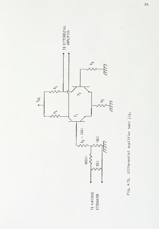
one of the transistors of the pair as sho.vn in Fig. A _9. The noise of
each transistor is measured separately in the common emitter connection
using the measurement system of Fig. A~l and the test jig of Fig. A -3.
The burst noise and noise resistance of the compound Darlington
connection of transistors are measured using the circuitry of
Fig. A-10. The collector current ratio is varied by varying the
current source current control resistor R. The variation of burst
noise output current and amplifier noise resistance as a function of
current are determined using the two major systems described earlier.
The measurement systems of this chapter provide the instrumentation
necessary to verify the theory presented in Chapters Two, Three, and
Four.

83
I h
Z.
a
vwv
T
00I
<
8k
I ywv5
a
VW^-^W^r
a
nAA^

85
BIBLIOGRAPHY
1. A. van der Zell, "Noise in junction transistors," Proc. IRE.,
vol. 46, pp. 1019-1033, June 1958.
2. L. J. Giacoletto, "The noise factor of junction transistors,"
in Transi stors I . pp. 296~308, Princeton: RCA Laboratories, 1956.
3. W. Guggenguehl, and M. J. 0. Strutt, "Theory and experiments of
shot noise in semiconductor diodes and trans is tors ," .Erne,—LBJl,
vol. 45, pp. 839-857, June 1957.
k. W. H. Fonger, "A determination of 1 /f noise sources in semi-
conductor diodes and tr i odes', 1
inXr_sJis, i_stQrs I, pp. 239~295,
Princeton: RCA Laboratories, i 956.
5. C. T. Sah and F. M. h'ielscher, "Evidence of the surface origin
of the 1/f nnUp/ 1
physical RpvJP/j Letters, vol. 17, PP. 956"958,
October 1966.
6. G. Abcwitz, E. Arnold, E. A. Leventhal , "Surface states and 1/f
noise in mos t-^nqUfnrs/' IFF.P Trans. Electron Devices. , vol. ED~1 4,
pp. 375-379, November 1967.
7. J. F. Gibbons, "Lav frequency noise figure and its application to
the measurement of certain transistor parameters," .IRE Trans.
Flectron Devices , vol. ED"9, pp. 308"3 1 5, May 1962.
8. K. F. Knott, "1/f voltage noise in silicon planar bipolar
transistors," Electronic s Letters , vol. 4, pp. 555"556,
13 December 1968.
9. W. H. Card and P. K. Chaudhari, "Characteristics of burst noise,"
Proc. IEE ET
vol. 53, pp. 652-653, June 1965.
10. G. Giralt, J. C. Martin, F. X. Nateu-Perez, "Sur un phenomene
de bruit dan las transistors, caracte'r is e par des crelieaux de
coupant d 'amplitude constante," C. R. Acad. Sc. Paris,
vol. 261,
pp. 5350-5353, 1965.
11. P. E. Gray, D. De.-vitt, A. R. Boothboyd, J. F. Gibbons, Physical.
El ectronics and Circuit Models of Tran s istors , Chapter 4,
John Wiley and Sons, Inc., New York, 1964.
86

87
12. E„ R. Chenette, "Noise in semiconductor d ev i c es ," Advances _ In
Flee t, ron ics . vol. 23, L. Martin, ed. , Academic Press, 1967.
13. H. A. Haus £jl aj_. , "IRE standards on methods of measuring noise
in linear twoports," Proc. IRE ,vol. 48, pp. 60"68, January I960.
1 4. H. Rothe and W. Dahlke, "Theory of noisy fourpoles," P roc. IRE ,
vol. 44, pp. 811-318, June 1956.
15. D. K. C. MacDonald, Noise and Fluctuations; An Introduction,
pp. 3^-37, John Wiley & Sons, Inc., New York, 1962.
16. H. A. Haus .ai aJL. , "Representation of noise in linear twoports,"Proc. I RE, vol. 48, pp. 69-7 ;+, January I960.
17. R. D. Thornton .e_t aj_. , Handbook of Basic Transistor Circu it s and
Measurements , Chapter 9, John Wiley and Sons, Inc., New York, 1966.
18. E. R. Chenette, "Lav noise transistor amplifiers," Sol id StatePes ig n, pp. 27"30, February 1964.
19. C. T. Sah, "A nav semiconductor tetrode ~~ the surface-potentialcontrolled trans istor," P roc. IRE
,vol. 99, pp. 1623~1634,
November 1961.
20. F. Levenberger, "1/f noise in gate-controlled planar silicondiodes," Elect ronics L etters, vol. 4, p. 280, June 1968.
21. R. D. Thornton, 0. Dewitt, E. R. Chenette, P. E. Gray, C haract e r is tics
and Limitations of Tr ansis tors, Chapter 4, John Wiley and Sons, Inc.,
New York, 1966.
22. S. R. Hofstein, "Proton and sodium transport in S 1 ^ films,"IEEE Trans. El ectron D evices
,vol. 55, pp. 749"759, ^November 1967.
23.. E. Snow £l aj_. , "Ion transport phenomena in insulating films,"
A-iiPjiIigd Phy.sJ.cji., vol. 36, pp. 1669-1673, May 1965.
24. D. Wolf and E. Holler, "Bistable current fluctuations in
reverse biased p_n junctions of germanium," J. Appl ied Phys ics
,
vol. 38, pp. 189~192, January 1967.
25. G. Giralt, J. C. Martin, F. X. Nateu~Perez, "Le bruit en
crenaux des transistors plans au silicium," Elect ronics Letters,
vol. 2, pp. 228-230, June 1966.
26 . A . P a pou 1 i s , Probability, Random Variables and St ochastic Processes
,
Chapters 9 and 10, McGraw-Hill, Inc., New York, 1965.
88
27. P. E. Gray, D. Dewitt, A. R. Boothroyd, J. F. Gibions, Phys ica.l.
Electronics and Ci rcuit Models of Transistors, Chapter 3, JohnWiley and Sons, Inc., Ne.v York, 196^.
28. V. G. K. Reddi, "Influence of surface conditions on siliconplanar transistor current gain," Solid State Electronics
,vol. 10,
PP. 305-33^, 1967.
29. 0. Mueller, "Thermal feedback and 1/f flicker noise in semi-conductor devices," General Electric Technical Information Series,No. R6VCPD-12, November 20, 1964.

BIOGRAPHICAL SKETCH
Richard Charles Jaeger was born on September 2, 19^'t, in New
York, New York. He completed his secondary education in Fort
Lauderdale, Florida, in June, 1962, and entered the Un ivers i ty of
Florida in September, 1962. He received the degree of Bachelor of
Electrical Engineering with High Honors in April, 1966. Upon
receiving an NDEA Title !V graduate fellowship, he entered the
Graduate School of the University of Florida and was awarded the
degree of Master of Engineer ing. in December, 1966. Since that time
he has pursued studies leading to the degree of Doctor of Philosophy.
Richard Charles Jaeger is married to the former Joan Carol
Hill, and they have a son, Peter Charles Jaeger. He is a member of
Phi Kappi Phi, Tau Beta Pi, Eta Kappa Nu, Sigma Tau, the Institute
of Electrical and Electronics Engineers, and Kappa Sigma social
fraternity.
This dissertation was prepare
of the candidate's supervisory commi
members of that committee. It was s
d under the direction of the chairman
ttee and has been approved by all
ubmitted to the Dean of the College
tial
of Engineering and to the Graduate Council, and was approved as pari
fulfillment of the requirements for the degree of Doctor of Philosophy.
June 1369
Dean, College of Engineering
Dean, Graduate School
Supervisory Committee
I \dhdlAJSi
.'__

69 5 -fe