loss estimation in a voltage source inverter for...
TRANSCRIPT

UNIVERSITY OF PADUA
DEPARTMENT OF INFORMATION ENGINEERING
DEGREE IN ELECTRONIC ENGINEERING
Loss estimation in a voltage source inverter forelectrical drives
Student:Fabiano FOSSATO
Supervisor:Dott. Simone BUSO
Academic Year 2013/2014


To my parents.


Contents
1 Inverter 11.1 Half Bridge . . . . . . . . . . . . . . . . . . . . . . . . . . . . . . . . . . . . . . . . . 11.2 Full Bridge . . . . . . . . . . . . . . . . . . . . . . . . . . . . . . . . . . . . . . . . 21.3 PWM modulation . . . . . . . . . . . . . . . . . . . . . . . . . . . . . . . . . . . . . 21.4 Switching Devices . . . . . . . . . . . . . . . . . . . . . . . . . . . . . . . . . . . . 4
I Theoretical Analysis 7
2 Modelling of the losses 92.1 General view . . . . . . . . . . . . . . . . . . . . . . . . . . . . . . . . . . . . . . . 92.2 Thermal equivalent circuit . . . . . . . . . . . . . . . . . . . . . . . . . . . . . . . . . 112.3 Average estimation of the losses . . . . . . . . . . . . . . . . . . . . . . . . . . . . . 132.4 Instantaneous estimation of the losses . . . . . . . . . . . . . . . . . . . . . . . . . . 16
3 Calculation of the losses 173.1 Average calculation of the losses . . . . . . . . . . . . . . . . . . . . . . . . . . . . . . 173.2 Instantaneous calculation of the losses . . . . . . . . . . . . . . . . . . . . . . . . . . 183.3 Simulations . . . . . . . . . . . . . . . . . . . . . . . . . . . . . . . . . . . . . . . . 20
II Practical Analysis 23
4 Choosing the components 254.1 The Microcontroller . . . . . . . . . . . . . . . . . . . . . . . . . . . . . . . . . . . . 254.2 Driver . . . . . . . . . . . . . . . . . . . . . . . . . . . . . . . . . . . . . . . . . . . 264.3 Power supply . . . . . . . . . . . . . . . . . . . . . . . . . . . . . . . . . . . . . . . . 274.4 Current sensor . . . . . . . . . . . . . . . . . . . . . . . . . . . . . . . . . . . . . . . 28
5 Designing the board 295.1 Electrical schematic . . . . . . . . . . . . . . . . . . . . . . . . . . . . . . . . . . . . 295.2 Printed circuit . . . . . . . . . . . . . . . . . . . . . . . . . . . . . . . . . . . . . . . 295.3 Realising the board . . . . . . . . . . . . . . . . . . . . . . . . . . . . . . . . . . . . 325.4 Testing the board . . . . . . . . . . . . . . . . . . . . . . . . . . . . . . . . . . . . . 335.5 Conclusion . . . . . . . . . . . . . . . . . . . . . . . . . . . . . . . . . . . . . . . . 36
V


Chapter 1
Inverter
In this chapter we will talk about the theoretical analysis of an inverter, analysing the differentconfigurations, the losses, the choice we have done and the models of the losses that we have used todefine which heat-sink to use.
1.1 Half Bridge
The half-bridge configuration is a type of configuration that can be used to realize an inverter. Themain advantage of this kind of configuration is its simpleness. Only few components are indeed necessary:two transistors in conjunction with two free-wheeling diodes. On the other hand, a three-wires DC sourceis required or more specifically, two DC voltage sources in input with a common wire.
A configuration like this can be obtained by means of a single DC input voltage realized with twoinput capacitors connected as shown in Fig.1.1 to obtain a common floating connection. An half-bridgeconfiguration, however, has the disadvantage to require a control of the switching devices in order toguarantee the same voltage across the input capacitors. A full-bridge configuration allows to overcomethis limitation. This is one reason why we decided to use a full-bridge configuration in this project.
Figure 1.1: Half-bridge configuration
1

2 CHAPTER 1. Inverter
How an half-bridge works
In this section we are going to discuss how an half-bridge works as it is essential to understandhow a full-bridge works. Let us consider that the load has both a resistive and a inductive part. Theinductance may be provided by the load (e.g. electric motor) or by a filtering device, used to filter thecurrent harmonics on the load.
Analysis: From the diagram in Fig. 1.1 it can be seen that there are two diodes connected in anti-parallel to each switching device. These diodes, called ”free-wheeling diodes”, assure a reclosing wayfor the current in every situation. In the case where the load is purely resistive these diodes are useless,but if the load is reactive they are fundamental to prevent a failure of the device. Usually, indeed, theswitching devices are current unidirectional so, if the current is forced by the load in the wrong direction,the devices will be destroyed. Thus, free-wheeling diodes are preferably used as they assure a reclosingway for the current in every operating condition. These diodes in power devices are currently included inthe package of each switch and usually they are not normal diodes, but the manufacturers take advantageto the internal structure of the switch. For example, thinking about the MOS-structure, there is a p-njunction between the body and the drain, this de facto represents the anti-parallel diode that we need.Designing accurately this junction, the manufacturers assure that this intrinsic diode can tolerate the samecurrent that pass through the MOS in the forward direction. In this way, the device becomes currentbidirectional even if the current flow is controllable only when it flows from the drain to the source.
Many power devices have an internal structure like this, so usually it is not necessary to use anexternal diode.
1.2 Full Bridge
The full-bridge structure is composed by two half-bridge blocks connected to the load. This con-figuration has many advantages compared to the half-bridge structure. First of all, it does not requirea complex control: in fact it is not necessary to control the voltage between the input capacitors. Thismakes completely free the way with which you can drive the transistors, except for the two transistors ofthe same half-bridge. The reason is that, if both the transistors of the same arm are on at the same time,there will be a short-circuit at the input. Another important advantage is the range of the output voltagethat with this configuration is 2Vin, the double of the previous case.
The main disadvantage is an higher hardware complexity of the driving systems, that must drive fourdifferent transistors. Furthermore, the losses are increased because the devices in series at the load arealways two: this means that the current flows through two devices that have a non-zero voltage drop,so the power dissipation is the double of the half-bridge configuration. As you can see from the circuitschematic in Fig. 1.1, the anti-parallel diodes are always present to guarantee a reclosing way for thecurrent. The evident advantages make this configuration often preferable to the half-bridge and, for thisreason, it will be used in this project. Another motivation for choosing this solution in this study is thatwe use an high voltage source, so the higher voltage drop across the two transistors is not so relevant.Consequently, one of the biggest disadvantage of this configuration can be avoided.
1.3 PWM modulation
Above we have described the inverter configuration we are going to use in this project. The next stepis necessary to define the type of control we want to drive the transistors.
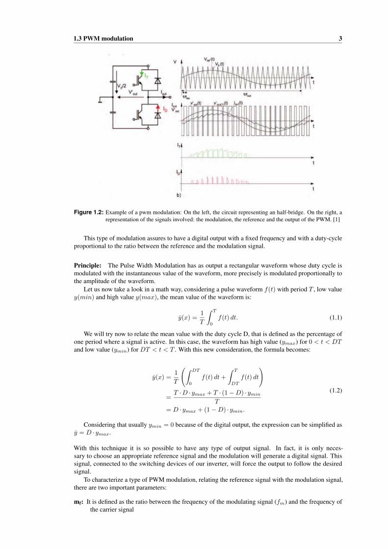
The most common driving system for the inverters, and also for a lot of other electronic devices, isthe Pulse Width Modulation (PWM). This type of modulation consists in comparing a reference signalwith a modulation signal, usually a high frequency sawtooth waveform. When the reference signal ishigher than the modulation signal, the PWM output is at high logical level. Conversely, if the referencesignal is lower than the modulation signal the PWM output is at low logical level. The PWM switchingfrequency has to be much faster than what would affect the load, which is to say the device that uses thepower. In this case the output main frequency is set to 50Hz. With this setting for the main frequency, thecorresponding frequency of the PWM usually has a range from few kHz to tens of kHz.
1.3 PWM modulation 3
Figure 1.2: Example of a pwm modulation: On the left, the circuit representing an half-bridge. On the right, arepresentation of the signals involved: the modulation, the reference and the output of the PWM. [1]
This type of modulation assures to have a digital output with a fixed frequency and with a duty-cycleproportional to the ratio between the reference and the modulation signal.
Principle: The Pulse Width Modulation has as output a rectangular waveform whose duty cycle ismodulated with the instantaneous value of the waveform, more precisely is modulated proportionally tothe amplitude of the waveform.
Let us now take a look in a math way, considering a pulse waveform f(t) with period T , low valuey(min) and high value y(max), the mean value of the waveform is:
y(x) =1
T
∫ T
0
f(t) dt. (1.1)
We will try now to relate the mean value with the duty cycle D, that is defined as the percentage ofone period where a signal is active. In this case, the waveform has high value (ymax) for 0 < t < DTand low value (ymin) for DT < t < T . With this new consideration, the formula becomes:
y(x) =1
T
(∫ DT
0
f(t) dt+
∫ T
DT
f(t) dt
)
=T ·D · ymax + T · (1−D) · ymin
T= D · ymax + (1−D) · ymin.
(1.2)
Considering that usually ymin = 0 because of the digital output, the expression can be simplified asy = D · ymax.
With this technique it is so possible to have any type of output signal. In fact, it is only neces-sary to choose an appropriate reference signal and the modulation will generate a digital signal. Thissignal, connected to the switching devices of our inverter, will force the output to follow the desiredsignal.
To characterize a type of PWM modulation, relating the reference signal with the modulation signal,there are two important parameters:
mf: It is defined as the ratio between the frequency of the modulating signal (fm) and the frequency ofthe carrier signal

4 CHAPTER 1. Inverter
mf =fcfm
. (1.3)
For high values of this parameter it could not be integer: in this case the PWM is called asyn-chronous and at the output are present some low level sub-harmonics. Vice versa, if the parameteris integer, the PWM is synchronous and the output has no sub-harmonics. This means that ifthis parameter if not so high it must be integer, otherwise the presence of the sub-harmonics isremarkable. In our case this is not a problem, fm is fixed at 50Hz and fc around 10kHz, so mf issizeable and it is also integer.
ma: The modulation factor is defined as the ratio between the amplitude of the modulation signal (Vm)and the amplitude of the carrier signal (Vc)
ma =VmVc
(1.4)
If ma < 1 (under-modulation) the modulation is linear and the amplitude of the fundamentalchanges linearly with ma. In addition to the fundamental there are harmonics of value mf , 2mf ,3mf and others, centered on these. In this range, the higher the modulation factor and the longerthe high side switch is on, the higher is the average load voltage. We can see this with the nextformula:
Vout = ma ·Vd2, (1.5)
where Vd is the input voltage of the inverter.
Ifma > 1 (over-modulation) the modulation is non-linear and there are more harmonic components,such that the fundamental could not be the biggest one.
Bipolar PWM: The bipolar PWM is so called because the switches 1-4 and 2-3 are driven in pair, theoutput in the first arm is exactly the opposite of the second arm, this means that:
VBo(t) = −VAo(t) (1.6)
this means that the output voltage could be written in this way:
Vo(t) = VBo(t)− VAo(t) = 2VAo(t) (1.7)
and the voltage peak of the fundamental harmonic is then:
Vo1(t) = maVd, for ma < 1 (1.8)
1.4 Switching DevicesCommercially the switching devices you can find are a lot, and the range of values they can cover is
considerable. Essentially, there are four main devices used in power electronics as switches:
Power MOSFET: These devices share with the normal MOS only the principle of operation, that is the”Field-Effect”, but technologically the normal MOSFETs and the power MOSFETs are completelydifferent devices. The power MOSFETs are able to stand current of hundreds of Amperes andvoltage till over 1000V. Anyway, the power MOSFETs share with the normal MOSFETs twoimportant features: they have the big advantage that they have no steady state losses due to thedriving and they have a fast switching time. On the other hand, they are more expensive and moresensitive to the overvoltage.
IGBT: This kind of devices are done mixing the structure of a MOSFET and of a BJT and for thisreason usually an IGBT is schematized like in figure 1.3. This combination of elements permitsto control the input like a FET and to use a bipolar transistor as a switch. This means that thisdevice is gate-drived so like a FET does not need a current to maintain its static condition but, likea bipolar transistor, it is capable of an high-current and a low-saturation-voltage. For this reason,

1.4 Switching Devices 5
these devices, fairly recent invention, are used in the medium-high power applications, usually in arange of current till more then 1500A and for switching voltage up to 3000V .
Figure 1.3: Symbol of an IGBT and equivalent circuit [2]
GTO, SCR: These components are used exclusively for very high power applications, with current tillmore then 3000A and voltage up to 7000V . They are, respectively, controllable at the switch onand not controllable during the switch off. This means that the SCRs can not be switched off by acontrolled signal, but they switch off only when the current that flows through stops by externalreasons. These devices can allow high current and high voltage, but they have the big disadvantagesof a long switching time. This limits the frequency they can operate. For high power applicationsthere are no others choices, so the only thing that you could do is to limit the frequency.
In applications like in this thesis we do not need to manage very high electrical quantities, so we canuse power MOSFETs or IGBTs. The IGBTs are a bit cheaper than the MOSFETs, they are less sensitiveto the overvoltages and they have also a lower voltage drop during the steady state conditions. On theother hand, they have a commutation time a bit longer than the MOSFETs, anyway in our case this is notso important because the switching frequency is not very high, for all these reasons we decided to use theIGBTs.


Part I
Theoretical Analysis
7


Chapter 2
Modelling of the losses
In this chapter we will talk about the losses in an IGBT and about two models for the evaluation ofthe losses.
2.1 General view
In power electronics, and particularly in the design of electronic converters, devices like IGBT, diodes,MOSFET and others are used as switches. The reason of this is that, ideally, a switch has no lossesconsidering that it has either zero current or zero voltage, so the power dissipation is always zero. By theway, these devices, even if used as switches, are not ideal switches: this means that they generate powerlosses. These inevitable losses occur both in static and switching conditions and, furthermore, there arealso power losses due to the driving of the switching devices.
The losses generated by the these devices used like switches are the most responsible of the losses inan electronic converter: they may increase the temperature till destroying completely the device. For thisreason, it is very important to evaluate these losses to assure that the temperature of the junction of thedevice remains under the maximum junction temperature specified in the data-sheet.
The total losses in a switching device can be divided in three main categories and then in some othersub-categories. The following graph explain these differences.
Total PowerLosses
Static Losses Switching Losses Driving Losses
On-StateLosses
BlockingLosses
Turn-onLosses
Turn-offLosses
These categories have not the same importance to the losses estimation: for example, often, thedriving losses are neglected since their contribution is a minimal part of the power losses. In powerelectronics this is reasonable since the purpose of this field of electronic is, somehow, to change thesize of the units of measurement like the voltage, the current and the frequency and doing that, trying toreduce the losses as much as possible, so it makes sense that the driving losses are neglected compared tothe other ones.
The other two big categories are the static losses and the switching losses or rather the losses duringthe conduction time interval and the losses during the commutation interval. In this thesis we use anIGBT device, so let us analize the losses specially for this kind of device.

10 CHAPTER 2. Modelling of the losses
IGBT: As discussed above, the driving losses can be neglected because they do not have a big influencein the calculation of the total losses: furthermore, also the blocking losses are usually neglected. Thisbecause when the IGBT is on, its voltage drop is not zero, but when it is off the leakage current is reallyclose to zero and so the power during the off-state. For this reason, normally, except for some extremeapplications, both the driving and the blocking losses are neglected. That is also what we are going to doin this case.
Let us now take a deeper look to the remaining categories, analysing their dependencies.
Regarding the on-state condition, an IGBT device has a behaviour similar to a bipolar device.This means that an electrical equivalent scheme of the device can be a constant voltage source – thatrepresents the Vce(sat) – with, connected in series, a resistance – representing the resistivity of thematerial – that correlate the losses with the current. For this reason we can say that the on-state powerdissipation (Pcond(T)) is dependent on:
• The load current over output characteristic VCE(sat) = f(Ic, VGE);
• The junction temperature;
• The duty cycle.
Concerning the switching losses, they are due to the not instantaneous changing of the electricalcharacteristics of the device: in fact, the variation is gradual and requires a delta-time to be completed,so in this time interval the power losses can be very high. For this reason, it is important that theswitching device changes its state as fast as possible. Furthermore, this kind of losses restricts themaximum switching frequency: in fact, if it is too high the switching losses can be more relevant than theon-state losses and also strongly compromise the efficiency of the system. We have to say that is noteasy to estimate the switching losses, because the waveform of the current and of the voltage during acommutation is very complicated and also dependent of various parameters. Anyway, at given controlparameters (RG, VGG) and neglecting parasitic effect (Ls, Cload), turn-on and turn-off losses (Pon, Poff) aremainly dependent on:
• The load current and the electric load type (ohmic, inductive, capacitive);
• The DC-link voltage;
• The junction temperature;
• The switching frenquecy.
With this new consideration, the total losses are now composed as follows:
Ptot(T ) = Pcond(T ) + Pon + Poff (2.1)
Obviously, this consideration is true only for a single IGBT, if there are more than one IGBTs youhave to multiply this formula for the number of the devices to have the total losses.
Freewheeling diode: Let us now analyse the losses in the freewheeling diodes. Like in the previousparagraph, where we decided to neglect the blocking losses for the IGBTs, for the same reasons the totalblocking losses may be neglected also in this case.
So far, the components of the power dissipation in the freewheeling diodes are three like for theIGBTs. Nevertheless, in this case, the turn-on losses may be neglected as well: in fact the turn-on powerdissipation is caused by the forward process and, as for fast diodes, this share of the losses may beneglected.
Like above, let us now analyse which are the variables that influence the on-state power dissipation.The on-state power dissipation (Pcond(D)) is dependent on:
• The load current (over output characteristic Vf=f(If));
• The junction temperature;
• The duty cycle.
At given control parameters of the IGBT commutation with the diode, and neglecting parasitic effects(Ls), turn-off losses (Prr) are dependent on:

2.2 Thermal equivalent circuit 11
• The load current;
• The DC link voltage;
• The junction temperature;
• The switching frequency.
The total losses for each freewheeling diode are composed as follows:
P tot(D) = P cond(D) + P rr (2.2)
Also in this case the previous formula concerns only a single diode, so to find out the right formula forthe total losses of a module we have to sum the total losses of an IGBT and of a diode and to multiplythat for the number of the switches presents in the device. The resulting formula, as follows:
P tot(M) = n(P tot(T) + P tot(D)) (2.3)
2.2 Thermal equivalent circuitNow we will treat how we can model the heat flow using an equivalent electrical model and how to
use that for our purposes. First of all, we are going to introduce the thermal resistance and the thermalcapacitance:
• The thermal resistance is a property that every object has: it represents a measurement of atemperature difference by which an object resists a heat flow;
• The thermal capacitance is a measurement of the physical quantity of heat energy required tochange the temperature of an object by a given amount.
The thermal equivalent circuit is used to simplify the treatment of the heat flow through a power deviceand its heat-sink: the heat flow is represented by current, the temperatures are represented by voltages, theheat source is represented by constant current sources, the absolute thermal resistances are representedby resistors and the thermal capacitances by capacitors.
The quantity of power dissipation Ptot due to the heat losses is expressed by the temperature differencebetween the device – usually this temperature is referred to the temperature of the junction, so it is calledTj – and the heat-sink (Ts):
∆T j-s = T j − T s. (2.4)
The thermal resistance between the junction and the heat-sink (Rth(j-s)) is defined as follow:
Rth(j-s) =T j − T s
P v. (2.5)
The thermal resistance is appropriate only during the stationary conditions, but regarding the transientcondition the thermal resistance become a thermal impedance Z th(j-s). Often, there is not only one thermalresistance to consider: for example, if the device has a base plate in the data-sheet usually there are twothermal resistances, one between the junction and the case Rth(j-c) and the other one between the case andthe flat plate Rth(c-s):
Rth(j-s) = Rth(j-c) +Rth(c-s). (2.6)
Obviously, if we have to consider also the transients, we have to take impedances and not resistances:
Z th(j-s) = Z th(j-c) + Z th(c-s). (2.7)
In power modules with base plate, the transistor and the free-wheeling diode are soldered together ona common copper substrate, thus being thermally coupled. In figure 2.1 are shown both the models: theequivalent thermal model with and without the base plate. The base plate matches the temperature of theIGBT and the freewheeling diode. This means that, for example, only the IGBT will heat the base platealso the diode will be warmed up, even if the diode itself does not contribute to the heating up of theplate.

12 CHAPTER 2. Modelling of the losses
Figure 2.1: In this figure there are two simplified thermal circuit diagrams of IGBT and freewheeling diode in apower module. On the left, a model for a module with copper base plate, on the right a module withouta base plate. [1]
In the figure 2.1 we may find several temperatures, called: Tj (temperature of the junction), Tc(temperature of the case), Ts (temperature of the substrate) and Ta (temperature of the ambient). As wecan see on the right picture there is not a case temperature, in fact it has not a base plate so, for the leftpicture the total thermal impedance will be:
Z th(j-a) = Z th(j-c) + Z th(c-s) + Z th(s-a); (2.8)
vice versa, on the right picture the case does not exist, so the formula is:
Z th(j-a) = Z th(j-s) + Z th(s-a). (2.9)
To obtain the chain-type equivalent circuit diagram, the factor time constants for the exponentialfunction are determined by means of formula manipulation.
Z th(x-y) = Rth1
(1− exp
−tτ th1
)+Rth2
(1− exp
−tτ th2
)+ ...
=
n∑v=1
Rthv
(1− exp
−tτ thv
) (2.10)
The parameters Rthv are usually specified in the data sheets of the devices, like the parameters τ thv: soit is possible to use the formula above and estimate correctly the temperature of the junction and choosethe correct heat sink.
Junction temperature: To evaluate the temperature of the junction it is first necessary to calculate thelosses of the device: after this is possible, having all the thermal impedances of the heating system and theambient temperature, to find out the temperature of the junction. This, obviously, is necessary to check ifthe specified device could work in that condition (power losses/heat sink) or not. To calculate correctly thetemperature of the junction considering the evolution of the system with time it is necessary to use thermalimpedances. Otherwise, with thermal resistances we can calculate the temperature under stationaryoperation conditions: this means that we have also to use stationary characteristics of the system. Theorder in which you have to proceed in this calculation is ”from the outside to the inside”, starting withthe ambient temperature and the thermal impedance of the heat-sink and then proceeding step by stepuntil reaching the junction temperature. The formula used for each step is: T i = T o + P v
∑Z th, where
T i is the inner temperature and T o the outer temperature.The scheme 2.2 is an example of the procedure to follow to calculate the temperature of the junction
of our device.

2.3 Average estimation of the losses 13
Figure 2.2: Calculation of the junction temperature under stationary condition [1]
Actually this scheme is very simple and the losses source is only one, but if there is more than onesource of losses, for example in a power switching device with IGBTs and freewheeling diodes, theformula changes in this way:
T i = T o + (P tot(T) + P tot(D))∑
Z th, (2.11)
where P tot(D) and P tot(T) are, respectively, the power losses of the diode and of the transistor. In case ofthe ”couples” transistor/diode should be more than one the above formula will change in accord to thecontribution of every couple:
T i = T o + n1(P tot(T) + P tot(D))∑
Z th. (2.12)
The semiconductor has a strong matching between the temperature and the losses, this means thatthe temperature influences the characteristics of the semiconductor. Considering this, it is not trivial tocalculate the losses: the easiest way is to calculate then considering the temperature of the junction at themaximum temperature. This ensures to take a conservative amount of the losses because the most ofthese increase with the temperature. A more accurate way to calculate the losses is taking account thetemperature to determinate the losses at a starting temperature (for example the ambient temperature)and then iteratively calculate the temperature and the losses until they will reach a stable value. This loopcan be easily solved by a computer and allows us to estimate more accurately the final temperature andthe losses of our device. The figure 2.3 explain in a graphic way how this technique works.
2.3 Average estimation of the lossesWe will now analyse the losses using the average characteristics of the system. Anyway, to calculate
correctly the losses we have to consider which kind of modulation we are going to use in our converter,that is PWM, already explained previously. In figure 2.4 you can see the half-bridge configuration withsome graphics that explain how the PWM works compared with the output quantity: in particular, youcan see that the output current is not exactly in phase with the output voltage and thus – considering theoutput current positive – the current flows in the IGBT when it is on and, when the IGBT is off, it flowsin the opposite direction through the diode.
The configuration in the figure is an half-bridge, whereas we are going to use a full bridge, but theother two switches (IGBT and relative diode) are driven complementary, so it is enough to consider anhalf bridge to estimate the losses. Furthermore, the two IGBTs of each half-bridge are on respectivelyonly in the positive or negative semi-sine, this means that we can analyse the losses only for one switchingdevice and then extend our considerations to the other three switches.
Even if we are considering an average model of the losses, the temperature of the junction is constantonly when the steady-state condition is reached: instead, during the transient it depends on different

14 CHAPTER 2. Modelling of the losses
Figure 2.3: Loop used to estimate the temperature and the losses in a semiconductors [1]
parameters, principally the AC output frequency, because it establishes how long each IGBT has to bein on-condition continuously. This means that a lot of parameters vary in time and could be difficult toestimate every single variation of these parameters. So we are going to define some simplification toallow us to calculate the instantaneous losses without considering useless parameters but, anyway, havingan acceptable estimation. The following simplification are assumed:
• Transistor and diode switching times are neglected;
• Junction temperatures are in time constant;
• Linear modulation (m ≤ 1);
• The switching frequency ripple of the AC current (sinusoidal current) is neglected;
• fsw fout.
We suppose that Vinv , the output voltage of the inverter, correspond to Vo, the voltage across the load(that in our case is supposed to be a machine). This means that the output impedance has a low drop atthe given frequency. The following expression represents the voltage across the load:
Vo(t) = Vo sin(ωt) =⇒ Vo(θ) = Vo sin(θ). (2.13)
Consequently, the average output voltage and the average voltage across the load can be forced to bethe same. We can so deduce the expression for the duty cycle related to the Vo:
V INV = VDCD(θ)− VDC(1−D(θ)) = VDC(2D(θ)− 1)!= Vo(θ) (2.14)
D(θ) =Vo(θ)
2VDC+
1
2=Vo(θ) + VDC
2VDC(2.15)
Using this expression of the duty cycle, we can proceed to calculate the average current that flowsthrough the IGBT and consequently the power dissipation. In fact, the average current can be calculatedas follows:
IS1 = D(θ)IL(θ) =V0(θ) + VDC
2VDCIL sin(θ + φ) (2.16)

2.3 Average estimation of the losses 15
Figure 2.4: Half-bridge configuration with the driving and output waveform [1]
This equation represents the average value of the current that flows through the IGBT S1 and S2 inthe first half period of each sine, so from an angle 0 to π. In the second half period, in fact, these twoIGBTs are off because the current is negative. This calculation is, in any case, a simplification becausewe have considered that if the average current is positive only the IGBT S1 and S2 can be on. This is nottrue , in fact, if the average current is close to zero, the instantaneous current can be negative even if theaverage is positive. Anyway this condition happen only for a limited time interval, so it is reasonable toneglect it.
According to the previous formula the power losses of one IGBT is:
PS1(θ) = VonIS1(θ) +RonI2S1RMS(θ) (2.17)
Where IS1RMS(θ) it is the RMS current that flows through the IGBT in one switching period.Consequently the power losses can be calculated like:
PS1 =1
2π
∫ 2π
0
PS1(θ) dθ =1
2π
∫ π
0
PS1(θ) dθ (2.18)
The IS1RMS(θ) is related by the current that flows through the load by the formula:
IS1RMS(θ) =√DILRMS(θ) (2.19)
In turn, the RMS current of the load can be decomposed as follows:
ILRMS(θ) =
√IL(θ) +
1
12∗∆I2LPP (θ) (2.20)
The ∆ILPP (θ) is the contribution of the ripple component and can be calculated as:
∆ILPP (θ) =VDC
2 − V02
2LfswVDC. (2.21)
Normally this contribution represent a negligible part of the current.According with the formulas we have just mentioned, and considering when the current can flow
through each device, it is possible to estimate the average losses of the IGBTs and the diodes.

16 CHAPTER 2. Modelling of the losses
2.4 Instantaneous estimation of the lossesIt is possible to realize a more accurate model considering the instantaneous values of the characteris-
tics of our inverter. Particularly, during the on-state condition the output voltage – and consequently theoutput current – change a lot during each sine, this means that also the temperature of the junction couldhave a purposeful variation during a period that can not be observed with the previous model. For thisreason is necessary to realize another model to check that this temperature rise does not exceed, also fora small time inteval, the temperature limit imposed by the datasheet.
In this model the on-state losses will be calculated just multiplying the instantaneous values of thecurrent with the associated value of the Vce across the IGBT and similarly, using the Vf , for the diode.The Vce and the Vf are parameters strongly related with the junction’s temperature of the device and withthe current that flows through it. For this reason it is necessary to realize a logic scheme to understandwhen actually each device is active in each moment.
Below, we can find the half-bridge schematic of the switching-device and the relative logic schemethat explains how each device switches related to the sign of the output current and the PWM signal. Thislogic scheme is shown in table below on the left and, on the right, the circuit diagram:
Device IOUT PWM1 PWM2
IGBT1 > 0 1 /DIODE1 < 0 / 0IGBT2 < 0 / 1DIODE2 > 0 0 /
Regarding the switching losses, as previously explained, it is difficult to estimate them correctly, butwe can consider the energy needed to change the logic state and multiply it for the switching frequency toobtain the power losses. Anyway, the switching energy losses are not a constant value, but change withthe temperature, the current and the voltage across the device. So, it is necessary to take into account this.By the way, using the datasheet it is possible to extrapolate these data and calculate properly the correctvalue of the energy. The formulas we are going to use are these:
Psw(I) = fsw ∗ E(on+off)(Tj , Iout, Vcc) (2.22)Psw(D) = fsw ∗ Err(Tj , Iout, Vcc) (2.23)

Chapter 3
Calculation of the losses
We have just analysed two ways to estimate the losses in a switching device, now we will see how todo this calculation and the relative results.
First of all we have to choose the switching device we want to use in this project: to do this we haveto fix some main parameters of the project, like:
• DC input voltage
• Output power
• Switching frequency
We have decided to design an inverter with an input voltage of about 300V, an output power ofabout 9kW and a switching frequency of 10kHz. The output voltage will be, according to the full-bridgestructure, at most 300V with a maximum output current, in any case related to the others characteristics,around 30A.
Once fixed this parameter, is possible to choose the switching device: in this case, we choose theINFINEON F4-30R06W1E3. It has four IGBTs connected internally in a full-bridge configuration andeach IGBT has his own freewheeling diode. Furthermore, there is also a NTC temperature sensor tocheck the real temperature of the device so, in case, it is possible to switch-off the converter preventing afailure of it. According to the data-sheet the IGBTs can tolerate a ”Nominal current (in DC condition)”of 30A with a ”Repetitive peak current” of 60A and the ”Maximum Vce voltage” allowed is 600V. Thecharacteristics of the freewheeling diodes are almost the same of the IGBTs, they can tolerate the samecurrent, but the ”Maximum repetitive reverse voltage” is 600V.
3.1 Average calculation of the losses
Now we are going to calculate the losses using the model explained in the section 2.3 and to makethis calculation we used SIMULINK®. First of all, we speak about the temperature model. It is modelledusing the datasheet: in fact, for each IGBT and diode there are four different thermal resistances fromthe temperature of the junction till the base plate, each one with its own value of thermal resistance andthermal capacitance. The values are reported as follows:
IGBT
i: 1 2 3 4
ri[K/W ] 0,126 0,274 0,637 0,514τi[s] 0,0005 0,005 0,05 0,2
Diode
i: 1 2 3 4
ri[K/W ] 0,233 0,398 0,719 0,5τi[s] 0,0005 0,005 0,05 0,2
17
18 CHAPTER 3. Calculation of the losses
These reported above are the thermal impedances of the switching devices, but to our model we haveto add also the thermal impedance of the heat-sink. We fixed the value of it to 0.5K/W , with a τ of0.1s. We have to say that, in this case, the parameter τ is not fundamental because the important thing isthe maximum temperature reached by the junction and not in how much time. For this reason it can bechanged to make the simulation faster.
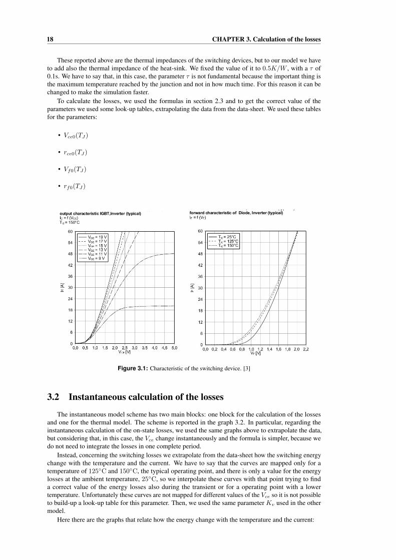
To calculate the losses, we used the formulas in section 2.3 and to get the correct value of theparameters we used some look-up tables, extrapolating the data from the data-sheet. We used these tablesfor the parameters:
• Vce0(TJ)
• rce0(TJ)
• Vf0(TJ)
• rf0(TJ)
Figure 3.1: Characteristic of the switching device. [3]
3.2 Instantaneous calculation of the losses
The instantaneous model scheme has two main blocks: one block for the calculation of the lossesand one for the thermal model. The scheme is reported in the graph 3.2. In particular, regarding theinstantaneous calculation of the on-state losses, we used the same graphs above to extrapolate the data,but considering that, in this case, the Vce change instantaneously and the formula is simpler, because wedo not need to integrate the losses in one complete period.
Instead, concerning the switching losses we extrapolate from the data-sheet how the switching energychange with the temperature and the current. We have to say that the curves are mapped only for atemperature of 125C and 150C, the typical operating point, and there is only a value for the energylosses at the ambient temperature, 25C, so we interpolate these curves with that point trying to finda correct value of the energy losses also during the transient or for a operating point with a lowertemperature. Unfortunately these curves are not mapped for different values of the Vce so it is not possibleto build-up a look-up table for this parameter. Then, we used the same parameter Kv used in the othermodel.
Here there are the graphs that relate how the energy change with the temperature and the current:

3.2 Instantaneous calculation of the losses 19
Figure 3.2: Global view of the instantaneous losses model implemented with SIMULINK®
Figure 3.3: Characteristic of the switching device. [3]

20 CHAPTER 3. Calculation of the losses
3.3 Simulations
In this section we will compare the various models, and we will discuss the results. In addition to thetwo models realised we are going to compare the results with another model. In fact in the INFINEONwebsite there is a simulation tool with which you can simulate the temperature of the junction and thepower losses, just choosing your device and some main parameters like the switching frequency, theinput DC voltage, ecc. Anyway, we can not choose which kind of output we would like to have, so it ispossible to compare this model only for a limited type of data.
Figure 3.4: IGBT’s power losses function of the currentFixed parameters: m = 0.7, VDC = 300V, cos(ϕ) = 0.9, Ta = 25C
Figure 3.5: Diode’s power losses function of the currentFixed parameters: m = 0.7, VDC = 300V, cos(ϕ) = 0.9, Ta = 25C
Figure 3.6: IGBT’s temperature function of the currentFixed parameters: m = 0.7, VDC = 300V, cos(ϕ) = 0.9, Ta = 25C

3.3 Simulations 21
Figure 3.7: Diode’s temperature function of the currentFixed parameters: m = 0.7, VDC = 300V, cos(ϕ) = 0.9, Ta = 25C
As we can see in the graph above the three models give similar results, except for the temperature ofthe IGBT. In fact the temperature of the INFINEON model is significantly higher than in the other twomodels. This because the INFINEON model considers, for the estimation of temperature, the maximumtemperature reached. Instead, in our models, the temperature in each point is calculated, also in theinstantaneous one, as the average value in one period. In this way it is possible to compare the results ofthe two models we realized.
Anyway, it is possible to compare the temperature of the instantaneous model and of the INFINEONmodel printing a graph with the temperature’s evolution in one period, once the steady state condition isreached. The graphs that follow represent the comparison of the temperature’s evolution between thesimulink model and the INFINEON model at the nominal conditions (Vin = 300V, Iout = 30A, m = 1).In this graphs we can see that the temperature’s trend of the IGBT and of the diode are really similar forboth models, and also the average temperature of the IGBT is similar. The average IGBT temperature ofthe simulink model is around 75C and around 70C for the INFINEON model, instead, regarding thediode, also if the trend is very similar the average temperature is a bit more different, with a value around43C for the simulink model and around 35C for the INFINEON model.
Figure 3.8: Instantaneous trend of the IGBT and diode’s temperature during one period using the SIMULINKmodel

22 CHAPTER 3. Calculation of the losses
Figure 3.9: Instantaneous trend of IGBT and diode’s temperature during one period using the INFINEON model

Part II
Practical Analysis
23


Chapter 4
Choosing the components
As said previously, the switching device we are going to use is an INFINEON F4-30R06W1E3, sonow we need to choose the other components to realise our inverter. Usually, to drive an inverter, thereare two possibilities: use a microcontroller or an external PWM generator. In the second case the inverterwill not be completely independent, so we decided to use a microcontroller.
4.1 The Microcontroller
Commercially, there are many types of microcontrollers for every kind of application, in particularsome of these have also outputs designed specifically to generate a PWM signal. For this reason, it is agood idea to choose a component with this characteristic. Furthermore, the clock frequency is important,in fact our inverter works with a switching frequency of 10kHz, so the microcontroller must work fasterthan this frequency to assure that every process will be completed in, at most, 100µs. This actually is nota problem: in fact, commercially, the clock frequency of the microcontroller is usually higher that 1MHz,often many hundreds. For these reasons, it is not difficult to find a proper microcontroller.
We chose a microcontroller produced by Texas Instrument called TMS320F28335. It has twelvedifferent outputs suitable to work with a PWM signal: furthermore, the clock frequency is 150MHz,more than what we need for this project. Anyway, this project, besides the PWM pins, requires someinput/output pins that this microcontroller has. In particular, using the inputs it is possible also to connectsome sensors: for example, to check the output current or the temperature of the switching device. Itis also possible to use these pins, as we can see later, to simplify the testing of the board or to disablequickly the inverter in case of necessity. The microcontroller we have used is mounted on a board ”readyto use”, where every useful pin should be connected – means a connector – to the other devices, and allthe other pins are managed by the board.
Regarding the software it is possible to program this kind of microcontroller using SIMULINKand then, through MATLAB, to generate the C-code for a specific microcontroller. Once the C-code isgenerated it is finally possible to load it in the microcontroller or to launch a debug session.
Figure 4.1: Board of the microcontroller TMS320F28335
25

26 CHAPTER 4. Choosing the components
Figure 4.2: Scheme of the software
SoftwareIn figure 4.2 there is the SIMULINK scheme of the software, as we can see it appears very simple: on
the bottom left there is a block called ”Target preferences F28335”, used to set some parameters relatedto the microcontroller and to allow the compiler to generate the code for the specific microcontroller.
On the top left, there is a block that represents the analog inputs. In this case we have used threeanalog inputs: one for the temperature of the switching device, one for the current and one for thereference signal. The first two signals are connected to two comparators and then to an ”and” operator tocheck if the temperature and the current are both under their respective limits. The output of this simplelogic is a digital output of the microcontroller. This output is physically connected to the enable pin ofthe two drivers. This is a simple way to protect the inverter, in fact, if the temperature or the current istoo high the inverter will be switched off till this two parameters will return under their limits.
Under the block to enable the drivers there is a block for the data transmission. In this case wedecided to transmit only the value of the current, but it is possible to transmit also the temperature orother internal parameters.
The last part of the scheme represents the generation of the PWM signals. The reference signal fromthe input is normalized from a maximum value of 4095 to 7500, as required by the following blocks,and then connected to the two blocks that generate the PWM signals. These two blocks will generate aPWM signal comparing the reference input signal with an internal sawtooth we have conveniently set.The relationship between the four output signals can be set as we want. Particularly, in this case we setthe output to work as two couples with opposite phase and with a proper dead-time.
We have to say that the external reference signal can be easily replaced by an internal signal generator.This block – during the compilation – will be replaced with a data-vector and then saved in the memory ofthe microcontroller. We realized also a software with an internal sine reference and it works without anyproblems, but for practical reasons we have used the external reference signal. In fact, with an externalreference, it is possible to change easily the parameters of the reference signal like amplitude, offset orfrequency; otherwise, it is necessary to modify the software and to recompile it, wasting a lot of timeduring the testing of the board.
4.2 DriverAs written previously, the microcontroller generates the PWM signals we need to drive our inverter,
anyway there is an electrical incompatibility. Indeed, the output of the microcontroller has a maximumvoltage of 3.3V and a current of few milliampere. The input of the switching device needs, instead,an input voltage around 15V with a peak current that should be some amperes. For this reason, it is

4.3 Power supply 27
necessary to use a device that smooths out these differences. This kind of devices are called driversbecause their role is to drive the switching device, when an appropriate input signal is supplied.
In this project we decided to use a dual IGBT driver IC produced by INFINEON, called 2ED020I12-FI. This device, as we can understand from the name, can drive two IGBTs, in particular two IGBTsof the same half-bridge. In fact it has a special protection to prevent short circuits. If both the inputsignals to drive the two IGBTs are on, the output will be disabled till when this situation will be changed.In addition to this special characteristic the driver can tolerate an output voltage of ±1.2kV, an outputcurrent of +1/− 2A and a power supply from 14 to 18V .
The IGBTs need two different voltages – one positive and one negative – to assure a fast switching.This driver has not a double input power supply: anyway, using a trick it is possible to realise thisconfiguration. The two outputs of a driver are in fact totally insulated because the emitters of the twoIGBTs are connected to two different points of the circuit. Using this characteristic it is possible to realisethe configuration in figure 4.3 to obtain two driving voltage.
Figure 4.3: Switching management of one IGBT
4.3 Power supplyAs explained in the previous section, it is necessary to use an external power supply for the drivers.
Each IGBT must be driven with two different voltages: one positive to switch-on the IGBT and onenegative to switch it off. The positive voltage usually is around 15V and must be higher then a minimalvalue to guarantee a correct switch-on of the IGBT. The negative voltage instead is not strictly necessarybecause to switch-off an IGBT is sufficient to short-circuit the gate with the emitter, removing the chargein the gate-body capacitor. Anyway, to guarantee a fast switch-off of the device – necessary to reducethe losses – usually the IGBTs are switched-off with a negative voltage. In this project we fixed thepositive voltage to 15V and the negative to −3.3V. Remembering the full-bridge configuration we caneasily see that every IGBT is connected to a different point of the circuit. This means that to guarantee agalvanic isolation it is necessary to use a different power supply for each IGBT, or rather two: one for theswitch-on and one for the switch-off. Considering this, we need eight different power supplies to drivecorrectly our IGBTs.
Every IGBT has the same behaviour and we are also going to use the same circuit configurationfor each one, so it is sufficient just to design the power supply for one IGBT and then to use the sameconfiguration for the other switches.
We proceed calculating the energy required to switch one IGBT. An IGBT can be considered as acapacitor, and the value of this capacitor is reported in the datasheet: in particular, for this IGBT thevalue of the equivalent capacitor is estimated to be 0.3µF. Let us now calculate the power required toswitch one IGBT:
E = CV 2 = 0.3µF(15V − (−3.3V))2 = 0.3µF(18.3V))2 = 0.1mJ (4.1)
P = E ∗ fsw = 0.1mJ ∗ 10kHz = 1W (4.2)
The power we found is the average value of the power required in a period, but the peak value can bemuch higher then 1W: for this reason we put a big capacitor (of 10µF) at the output of the converters.

28 CHAPTER 4. Choosing the components
Now, knowing the value our converters must be able to supply we choose two converters produced byTRACO POWER, called TME0515S and TME0503S, respectively to generate 15V and −3, 3V.
4.4 Current sensorWe decided also to install a current sensor for two reasons. First of all to prevent a damage of the
device: for example, if the load is too small and so the peak current if too high, it is possible to disableinstantaneously the IGBT preventing a failure of the device. The second reason is because with thiscomponent it is possible to control the inverter with a current loop, improving the behaviour of ourinverter in every condition, specially when any parameter change over time.
We decided to use a LEM CASR 25-NP. It has a current measuring range between −85 to 85A, itneeds a power supply of 5V and an output voltage from 0, 375V to 4, 625V with a reference voltage of2, 5V at 0A.

Chapter 5
Designing the board
We have just discussed the components we are going to use to realise our inverter. In this chapter wewill talk about how the board was designed, initially talking about the electrical schematic and then theprinted circuit (PCB).
5.1 Electrical schematicTo realise the schematic circuit we used the software EAGLE. A picture of the electrical schematic
of our project is reported in picture 5.1. On the left side there are 3 connectors: The one on the top is aconnector for a serial protocol communication system that can be used to pass some information to anexternal device; under this there are another two connectors: one for the 5V power supply and anotherone for the DC voltage supply of the inverter.
Between these connectors there is a circuit with a diode used to easily understand when then logicalpart of the board is powered. As we can note the ground signals of the connector for the communicationsystem and the for the 5V power supply are called differently. This because on one hand the digitalsignals are very fast and they can influence the values of the analog signals changing over time the valueof the ground and, on the other one, the current flow of the analog current can make the voltage level ofthe ground different around the board and this can compromise the digital communications.
The big connector called TI DSP is the connector of the microcontroller. There are connected thePWM signals, the power supply, others analog inputs and some other signals necessary to program themicrocontroller. These last signals are connected to another connector reported under it, that is necessaryto connect the programmer. In this case, like in some other part of the schematic, the connections arenot made by a wire, but using some labels to simplify the view of the schematic. On the right of themicrocontroller’s connector there is another small one used to connect some external signals to themicrocontroller. These extra signals can be useful during the test of the board, for example to use anexternal reference signal for the PWM, as we did.
On the right of all these connectors there are some blocks that represent the 2 drivers (the bigger ones)and the relative power supply. The drivers have in input the PWM signals and a signal to enable/disablethe drivers and so the inverter. At the output there are the signals to drive the IGBTs. In addition there arethe various power supply for the drivers, provided in input with 5V and in output with the +15/− 3.3Vof the DC/DC converters, represented by the four small blocks over and above each driver.
The output signals of the drivers are connected by some resistances to the switching block. Theresistance are three connected in series for each IGBT, this because the values of the resistances arecommercially standardized, so in this way is easier to have the exact value of resistance we want.
On the right side of the switching device there is the AC output of the inverter. One of the two outputwires is connected directly to a connector and the other one passes through the sensor current and then tothe connector on the right side of the schematic.
5.2 Printed circuitIn this project there are different kinds of signals (analog, digital and power) and every one has
different necessity: for this reason we used a four layer board. Two layers are completely dedicated tothe power supply and this means that: the 5V supply for the microcontroller, the DC input of the inverter
29

30 CHAPTER 5. Designing the board
3V
3/5
V
5V
+5V
+5V+5V
VDD
VSS
VSS VDD
10u
10u100n
100n
15
TI_DSP
+5V
+5V
+5V
+5V
+5V
+5V +5V
>VA
LU
ES
+5V
+5V
15
15
15
15
15
15
15
15
15
15
15
680
CAP-INVCAP-INV
100n
10u
100n
+5V
100n
DGND
AGND
AGND
AGNDAGND
AGND
AGND
DGND
DGND
DGND
DGND
AGND
AGND
AGND
AGND
AGNDAGNDAGNDAGND
AGND
AGND
AGND
+5VVA-0515S
VA-0515S
VA-0505S
VA-0505S
10u
10u
AGND
+5V
10u
10u
+5V
10u
AGND
10u
10u
+5V
10u
AGND
VA-0515S
VA-0505S
+5V
10u
AGND
10u
10u
+5V
10u
AGND
VA-0515S
VA-0505S
+5V
10u
AGND
10u
10u
AGND
X2-1
X2-2
SD
3
INH
1
INL
2
CP
O5
CP
+7
CP
-6
OP
O8
OP
+1
0
OP
-9
GN
D4
VH
S1
6
OU
TH
17
GN
DH
15
*2
GN
DL
11
OU
TL
12
VS
L1
3
SD
3
INH
1
INL
2
CP
O5
CP
+7
CP
-6
OP
O8
OP
+1
0
OP
-9
GN
D4
VH
S1
6
OU
TH
17
GN
DH
15
*2
GN
DL
11
OU
TL
12
VS
L1
3
C1
C2C3
C4
R1
U$5
12345678910
11
12
13
14
15
16
17
18
19
20
21
22
23
24
25
26
27
28
29
30
31
32
33
34
35
36
37
38
39
40
41
42
43
44
45
46
47
48
49
50
51
52
53
54
55
56
57
58
59
60
61
62
63
64
65
66
67
68
69
70
71
72
73
74
75
76
77
78
79
80
81
82
83
84
85
86
87
88
89
90
91
92
93
94
95
96
97
98
99
10
0
TM
S1
TD
I3
VR
EF
5
TD
O7
TC
K9
*2
EM
U0
13
TR
ST
N2
GN
D4
*4
EM
U1
14
U$6
R2
R3
R4
R5
R6
R7
R8
R9
R10
R11
R12
R13
E1
'E
1'
G1
G1
U3
U3
U2
U2
U1
U1
E2
'E
2'
G2
G2
V3
V3
V2
V2
V1
V1
G3
G3
E3
'E
3'
G4
G4
E4
'E
4'
PP
1*3
EU
EU
1*3
EV
EV
1*3
F4-30R06W1E3
T2
T2
T1
T1
P$
1P
2_
A*3
P$
2P
1_
A*3
P$
1P
2_
A*3
P$
2P
1_
A*3
X1-1
X1-2
X1-3
U$9
U$10
C6
C7
C10
I-INP
$1
*3I-O
UT
P$
8*3
VC
P$
14
GN
DP
$1
3
OU
TP
$1
2
RE
FP
$1
1
C11
LED1
R14
DC1
+V
IN2
-VIN
1
+V
OU
T4
-VO
UT
3
DC2
+V
IN2
-VIN
1
+V
OU
T4
-VO
UT
3
DC7
+V
IN2
-VIN
1
+V
OU
T4
-VO
UT
3
DC8
+V
IN2
-VIN
1
+V
OU
T4
-VO
UT
3
C12
C13
C5
C14
C15
C16
C17
C8
DC3
+V
IN2
-VIN
1
+V
OU
T4
-VO
UT
3
DC6
+V
IN2
-VIN
1
+V
OU
T4
-VO
UT
3
C18
C19
C20
C21
DC9
+V
IN2
-VIN
1
+V
OU
T4
-VO
UT
3
DC10
+V
IN2
-VIN
1
+V
OU
T4
-VO
UT
3
C22
C23
C24
JP1123456
JP212
15V_1
15V_1
15V_215V_2
15V_3 15V_3
0V_2
15V_415V_4
0V_4
EPWM1A
EPWM1B
EPWM2A
EPWM2B
DOT-SD
DOT-SD
DOT-SD
DOT-SD
TDI
TDI
TDO
TDO
TMS
TMS
TRSTN
TRSTN
EMU1
EMU1
EMU0
EMU0
TCK
TCK
0V_1
-3V3_1
-3V3_2
-3V3_2
0V_3
-3V3_3
-3V3_3
-3V3_4
-3V3_4
+
++
+
+
DC
/DC
CO
NV
ER
TE
R
DC
/DC
CO
NV
ER
TE
R
DC
/DC
CO
NV
ER
TE
R
DC
/DC
CO
NV
ER
TE
R
++
++
+
++
+
DC
/DC
CO
NV
ER
TE
R
DC
/DC
CO
NV
ER
TE
R
+
++
+
DC
/DC
CO
NV
ER
TE
R
DC
/DC
CO
NV
ER
TE
R
+
++
Figure 5.1: Electrical schematic of the inverter

5.2 Printed circuit 31
and the AC output wires are realised in the same two layers. These 2 layers are placed in the middle ofthe board to prevent any dangerous situation for users. The other 2 layers are used for all the signals andalso for the power supply of the drivers. In picture 5.2 we can see the final project of the board with allthe layers.
The big pink layer represent the 5V power supply of the board and the light blue one the relativeground. These two layers gave us the big advantage to easily power the various devices. In fact, if thelayer passes under the specific point where we need power, the connection will be realised just using avia.
On the bottom left part of the board there are the two wires of the DC input power, specifically thepink one is the positive voltage and the light blue the ground. Instead on the bottom right, precisely afterthe switching device, there is the AC output voltage of the inverter. As we can see the two wires are asmuch width as possible because of the big current they have to tolerate. Also the thickness of these layersis bigger than for the other two for the same reason. In particular the manufacturer of the board suggeststo use a wire at least 0.1mm width for each Ampere that has to flow in that wire. All the devices weremounted on the top side of the board, except for the switching device that is mounted on the bottom sidebecause is necessary to fix it on the heat-sink.
Designing the board we tried, when it was possible, to follow some rules, in particular:
• Minimize the length and the distance of the wires that connect the drivers and the switching deviceto reduce the parasitic inductances.
• Use vias only for slow signals.
• Separate the board in a ”signal area” and in a ”power area”.
• Minimize the distance of the filtering capacitor to the devices.
As we can see the board is divided in two main areas. On the bottom part there is the ”power area”with, starting from the left: the DC input connector, the capacitor of the DC-link, the switching device,the current sensor and the AC output connector.
Instead, on the upper part there is the ”signal area” with, starting from the left: the 2-pin connectorfor the 5V power supply and the 3-pin connector for the serial communication port, the strip connectorfor the analog input of the microcontroller, the big connector of the microcontroller, the 2 drivers withthe filtering capacitors and the relative power supply and, on the right, the connector to program themicrocontroller.
On the board are present 6 holes, 4 on the corners to fix the board to a stand and 2 to fix the switchingsystem to the heat-sink.
In picture 5.3 we can see the board without the four power layers, so we can appreciate better thesignal wires. As we can see the most of them are on the top of the board, and all the vias are used forslow signals. Something that we can not see from these pictures is that the analog and the digital groundare connected together in one point corresponding to the 3-pin connector. This assure that the digitalground signal is not influenced by the current that flows through the analog ground.

32 CHAPTER 5. Designing the board
Figure 5.2: Printed circuit
Figure 5.3: Printed circuit without the power layers
5.3 Realising the board
The board was produced by an external producer and then assembled in the university laboratories.On the top view picture (fig: 5.3) we can see the wires and the pad of the SDM devices.
Initially, as we can see in the picture 5.5, the board was tested without the heat-sink. This to checkwith low power if everything was fine. The board was tested in this condition with a voltage less then 10Vand a current less than 1A. Once we checked some basic characteristics – like the dead-time – the boardwas equipped with an heat-sink provided of a fan and put inside a ”safety box”. The safety box must beused for several reasons. In fact, this inverter works with high values of voltage and of current and alsothe temperature of the DC-link capacitors and of the heat-sink can be high enough to hurt. Furthermore,we have to remember that the maximum power of this inverter is around 9kW and if something goeswrong – for example a short circuit due to a dead-time too short – the device could explode or catch fire.
Here below we can find some picture of the realising process. In order: the board without anycomponent, the board during the soldering process, the board completely assembled and the board withthe heat-sink inside the safety box.

5.4 Testing the board 33
Figure 5.4: Board completely mounted in the safety box
5.4 Testing the boardAs written above initially the board was tested without the heat-sink as we can see in picture 5.5.
The first step was to test the inverter without any external load and check the output voltage startingwith a low value of the input and increasing it till the nominal value. We did this test to check if thedead-time was long enough. In fact, if the dead-time is not sufficient, the output voltage will have somenegative peaks during each switching due to a temporary short-circuit of one arm. If these voltage peaksare too big they can cause a big current peak, increasing very quickly the temperature of the junction anddecreasing the efficiency or, in the worst case, destroying the component. To fix a value of the dead-time
34 CHAPTER 5. Designing the board
we proceeded starting with a very big dead-time (around 10µs) and decrementing it till few µs. Thepicture 5.6 represent the output voltage of the inverter with an input voltage of 300V and no load. Aswe can see there are some peaks but they are not so big. We have in fact also to consider that there isnot any capacitor at the output to maintain a stable value, so a little bit of ”noise” is understandable. Forthis reason we decided that this kind of peaks was acceptable and we stopped the decrementing of thedead-time at 1, 36µs.
Once we have fixed the dead-time we initially tested the inverter (still without the heat-sink) with alow power and only with a resistive load, then with a ohmic-inductive load: precisely with 25Ω in seriesto an inductance of 3.13mH. In picture 5.7 we can see the trend of the output current during the firsttest without heat-sink. We can see that the signal is pretty similar to a sinusoid but when the value ofthe current is close to zero it results deformed. This is due to the very low value of the current we wereforced to use because of the absence of the heat-sink. In this case the peak value of the current is around160mA (the probe attenuation is 20). In fact, if the current that flows through the IGBTs it is too lowthey do not work in the saturation zone, but in the linear one, deforming the sinusoid. Anyway, except forthis problem the inverter seems to work fine, so we proceeded to build the heat-sink and the safety box totest the board at the nominal condition.
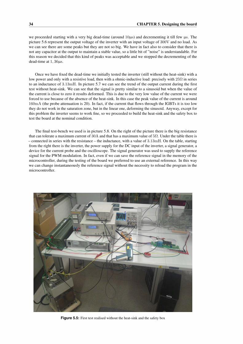
The final test-bench we used is in picture 5.8. On the right of the picture there is the big resistancethat can tolerate a maximum current of 30A and that has a maximum value of 5Ω. Under the table there is– connected in series with the resistance – the inductance, with a value of 3.13mH. On the table, startingfrom the right there is the inverter, the power supply for the DC input of the inverter, a signal generator, adevice for the current probe and the oscilloscope. The signal generator was used to supply the referencesignal for the PWM modulation. In fact, even if we can save the reference signal in the memory of themicrocontroller, during the testing of the board we preferred to use an external reference. In this waywe can change instantaneously the reference signal without the necessity to reload the program in themicrocontroller.
Figure 5.5: First test realised without the heat-sink and the safety box

5.4 Testing the board 35
Figure 5.6: Vout of the inverter with an input voltage of 300V and no load
Figure 5.7: Test of the board with no load and no heat-sink with a low value of the current

36 CHAPTER 5. Designing the board
Figure 5.8: Final test configuration
5.5 ConclusionThe final purpose of our project was to test completely the inverter and to verify if the model matches
well the real trend of the losses. To check this it is necessary to know the thermal parameters of ourheat-sink, but these were not know. In fact, the heat-sink that was installed in this inverter has not aknown value of thermal resistance. Anyway, to resolve this problem, is possible to measure this parametermeasuring at the same time the losses and the temperature of the heat-sink for different values of losses.Once this parameter is found it is possible to simulate the real working condition in the model and tocompare correctly the results. Anyway we had not the time to make this step, and we limit our work totest the inverter. Even if the inverter was designed to work with an input voltage of 300V and a current of30A, the power supply we had in the laboratory was not sufficient to test it at the nominal condition. Themain reason is that there was not a load capable to tolerate a power of 9kW for more than few seconds:this means that we tested our inverter with a current of 30A and with a voltage of 300V for a long lapseof time, but not at the same time. Anyway in both the conditions, and even with a current of 25A and aninput voltage of 200V the inverter worked properly with a modest increase of the heat-sink’s temperature.Reasonably also at the nominal conditions the increase of the temperature will be still limited, this maysuggest that the heat-sink is a bit oversized and if necessary, it can be replaced with a smaller one.

Bibliography
[1] NICOLAI U., WINTRICH A., TURSKY W., REINMANN T., 2011, Application Manual PowerSemiconductor, SEMIKRON International GmbH, Germany.http://www.semikron.com/download/assets/pdf/application_handbook/application_manual_complete.pdf
[2] SPIAZZI G., CORRADINI L., 2013, Appunti dalle Lezioni di elettronica per l’energia, Padova.
[3] Datasheet INFINEON F4-30R06W1E3www.infineon.com
37