logicore ip ahb-lite to axi bridge v2 - xilinx · pdf fileahb-lite to axi bridge v2.1 4 pg176...
TRANSCRIPT

LogiCORE IP AHB-Lite to AXI Bridge v2.1
Product Guide for Vivado Design Suite
PG176 December 18, 2013
AHB-Lite to AXI Bridge v2.1 www.xilinx.com 2PG176 December 18, 2013
Table of ContentsIP Facts
Chapter 1: OverviewAHB Interface . . . . . . . . . . . . . . . . . . . . . . . . . . . . . . . . . . . . . . . . . . . . . . . . . . . . . . . . . . . . . . . . . . . . . 5AHB Data Counter . . . . . . . . . . . . . . . . . . . . . . . . . . . . . . . . . . . . . . . . . . . . . . . . . . . . . . . . . . . . . . . . . 6Control Logic. . . . . . . . . . . . . . . . . . . . . . . . . . . . . . . . . . . . . . . . . . . . . . . . . . . . . . . . . . . . . . . . . . . . . . 6AXI4 Write Channel . . . . . . . . . . . . . . . . . . . . . . . . . . . . . . . . . . . . . . . . . . . . . . . . . . . . . . . . . . . . . . . . 6AXI4 Read Channel. . . . . . . . . . . . . . . . . . . . . . . . . . . . . . . . . . . . . . . . . . . . . . . . . . . . . . . . . . . . . . . . . 6Timeout Module . . . . . . . . . . . . . . . . . . . . . . . . . . . . . . . . . . . . . . . . . . . . . . . . . . . . . . . . . . . . . . . . . . 7Unsupported Features. . . . . . . . . . . . . . . . . . . . . . . . . . . . . . . . . . . . . . . . . . . . . . . . . . . . . . . . . . . . . . 7Licensing and Ordering Information . . . . . . . . . . . . . . . . . . . . . . . . . . . . . . . . . . . . . . . . . . . . . . . . . . . 7
Chapter 2: Product SpecificationStandards . . . . . . . . . . . . . . . . . . . . . . . . . . . . . . . . . . . . . . . . . . . . . . . . . . . . . . . . . . . . . . . . . . . . . . . . 8Performance. . . . . . . . . . . . . . . . . . . . . . . . . . . . . . . . . . . . . . . . . . . . . . . . . . . . . . . . . . . . . . . . . . . . . . 8Resource Utilization. . . . . . . . . . . . . . . . . . . . . . . . . . . . . . . . . . . . . . . . . . . . . . . . . . . . . . . . . . . . . . . . 9Port Descriptions . . . . . . . . . . . . . . . . . . . . . . . . . . . . . . . . . . . . . . . . . . . . . . . . . . . . . . . . . . . . . . . . . 10Register Space . . . . . . . . . . . . . . . . . . . . . . . . . . . . . . . . . . . . . . . . . . . . . . . . . . . . . . . . . . . . . . . . . . . 13
Chapter 3: Designing with the CoreClocking. . . . . . . . . . . . . . . . . . . . . . . . . . . . . . . . . . . . . . . . . . . . . . . . . . . . . . . . . . . . . . . . . . . . . . . . . 14Resets . . . . . . . . . . . . . . . . . . . . . . . . . . . . . . . . . . . . . . . . . . . . . . . . . . . . . . . . . . . . . . . . . . . . . . . . . . 14Memory Mapping . . . . . . . . . . . . . . . . . . . . . . . . . . . . . . . . . . . . . . . . . . . . . . . . . . . . . . . . . . . . . . . . 14Data Width . . . . . . . . . . . . . . . . . . . . . . . . . . . . . . . . . . . . . . . . . . . . . . . . . . . . . . . . . . . . . . . . . . . . . . 14Narrow Transfers . . . . . . . . . . . . . . . . . . . . . . . . . . . . . . . . . . . . . . . . . . . . . . . . . . . . . . . . . . . . . . . . . 15AHB-Lite Response Signaling. . . . . . . . . . . . . . . . . . . . . . . . . . . . . . . . . . . . . . . . . . . . . . . . . . . . . . . . 15AXI4 Response Signaling . . . . . . . . . . . . . . . . . . . . . . . . . . . . . . . . . . . . . . . . . . . . . . . . . . . . . . . . . . . 15Endianness . . . . . . . . . . . . . . . . . . . . . . . . . . . . . . . . . . . . . . . . . . . . . . . . . . . . . . . . . . . . . . . . . . . . . . 15Address/Data Translation . . . . . . . . . . . . . . . . . . . . . . . . . . . . . . . . . . . . . . . . . . . . . . . . . . . . . . . . . . 15Data Width Selection on AHB and AXI4 Interface . . . . . . . . . . . . . . . . . . . . . . . . . . . . . . . . . . . . . . . 16Bridge Timeout Condition . . . . . . . . . . . . . . . . . . . . . . . . . . . . . . . . . . . . . . . . . . . . . . . . . . . . . . . . . . 16Protection Signal Mapping from AHB-Lite to AXI4 Interface . . . . . . . . . . . . . . . . . . . . . . . . . . . . . . 17Timing Diagrams . . . . . . . . . . . . . . . . . . . . . . . . . . . . . . . . . . . . . . . . . . . . . . . . . . . . . . . . . . . . . . . . . 18
Send Feedback

AHB-Lite to AXI Bridge v2.1 www.xilinx.com 3PG176 December 18, 2013
Chapter 4: Customizing and Generating the CoreVivado Integrated Design Environment . . . . . . . . . . . . . . . . . . . . . . . . . . . . . . . . . . . . . . . . . . . . . . . 21Output Generation. . . . . . . . . . . . . . . . . . . . . . . . . . . . . . . . . . . . . . . . . . . . . . . . . . . . . . . . . . . . . . . . 23
Chapter 5: Constraining the Core
Chapter 6: Simulation
Chapter 7: Synthesis and Implementation
Chapter 8: Example DesignImplementing the Example Design. . . . . . . . . . . . . . . . . . . . . . . . . . . . . . . . . . . . . . . . . . . . . . . . . . . 28Simulating the Example Design. . . . . . . . . . . . . . . . . . . . . . . . . . . . . . . . . . . . . . . . . . . . . . . . . . . . . . 29
Chapter 9: Test Bench
Appendix A: Migrating and UpgradingMigrating to the Vivado Design Suite. . . . . . . . . . . . . . . . . . . . . . . . . . . . . . . . . . . . . . . . . . . . . . . . . 31Upgrading in the Vivado Design Suite . . . . . . . . . . . . . . . . . . . . . . . . . . . . . . . . . . . . . . . . . . . . . . . . 31
Appendix B: DebuggingFinding Help on Xilinx.com . . . . . . . . . . . . . . . . . . . . . . . . . . . . . . . . . . . . . . . . . . . . . . . . . . . . . . . . . 32Debug Tools . . . . . . . . . . . . . . . . . . . . . . . . . . . . . . . . . . . . . . . . . . . . . . . . . . . . . . . . . . . . . . . . . . . . . 34
Appendix C: Additional ResourcesXilinx Resources . . . . . . . . . . . . . . . . . . . . . . . . . . . . . . . . . . . . . . . . . . . . . . . . . . . . . . . . . . . . . . . . . . 35References . . . . . . . . . . . . . . . . . . . . . . . . . . . . . . . . . . . . . . . . . . . . . . . . . . . . . . . . . . . . . . . . . . . . . . 35Revision History . . . . . . . . . . . . . . . . . . . . . . . . . . . . . . . . . . . . . . . . . . . . . . . . . . . . . . . . . . . . . . . . . . 36Notice of Disclaimer. . . . . . . . . . . . . . . . . . . . . . . . . . . . . . . . . . . . . . . . . . . . . . . . . . . . . . . . . . . . . . . 36
Send Feedback

AHB-Lite to AXI Bridge v2.1 www.xilinx.com 4PG176 December 18, 2013 Product Specification
IntroductionThe ARM® AMBA® Advanced High Performance Bus (AHB-Lite) to AXI4 Bridge translates AHB-Lite transactions into AXI4 transactions. It functions as an AHB-Lite slave on the AHB bus and as an AXI4 master on the AXI4 bus.
Features• AXI4 interface is based on the AXI4
specif ication
• AHB-Lite interface based on the AHB specif ication
• Supports 1:1 (AXI4:AHB) synchronous clock ratio
• AHB and AXI4 data widths are the same and either 32/64-bit based on the configuration
• Supports narrow transfers on the AHB interface
• Supports burst termination on the AHB during which dummy transfers are initiated on the AXI4 interface
• Timeout feature to indicate no response from AXI4 slave during write and read transactions
IP Facts
LogiCORE IP Facts Table
Core SpecificsSupported Device Family(1) UltraScale™ Architecture, Zynq®-7000, 7 Series
Supported User Interfaces AXI4, AHB-Lite
Resources See Table 2-2.
Provided with CoreDesign Files VHDL
Example Design VHDL
Test Bench VHDL
Constraints File N/A
Simulation Model Not Provided
Supported S/W Driver N/A
Tested Design Flows(2)
Design EntryVivado® Design Suite
IP Integrator
Simulation For supported simulators, see the Xilinx DesignTools: Release Notes Guide.
Synthesis Vivado Synthesis
SupportProvided by Xilinx @ www.xilinx.com/support
Notes: 1. For a complete list of supported devices, see Vivado IP
catalog.2. For the supported versions of the tools, see the Xilinx
Design Tools: Release Notes Guide.
Send Feedback
AHB-Lite to AXI Bridge v2.1 www.xilinx.com 5PG176 December 18, 2013
Chapter 1
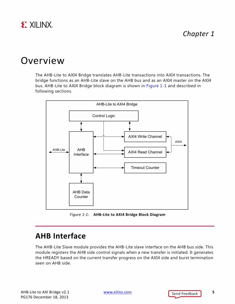
OverviewThe AHB-Lite to AXI4 Bridge translates AHB-Lite transactions into AXI4 transactions. The bridge functions as an AHB-Lite slave on the AHB bus and as an AXI4 master on the AXI4 bus. AHB-Lite to AXI4 Bridge block diagram is shown in Figure 1-1 and described in following sections.
AHB InterfaceThe AHB-Lite Slave module provides the AHB-Lite slave interface on the AHB bus side. This module registers the AHB side control signals when a new transfer is initiated. It generates the HREADY based on the current transfer progress on the AXI4 side and burst termination seen on AHB side.
X-Ref Target - Figure 1-1
Figure 1-1: AHB-Lite to AXI4 Bridge Block Diagram
Send Feedback

AHB-Lite to AXI Bridge v2.1 www.xilinx.com 6PG176 December 18, 2013
Chapter 1: Overview
AHB Data CounterThis module counts the valid data received from AHB for the write transfers. The count value is used to limit the HREADY generation after the required number of samples are received for the current transfer.
Control LogicThe control logic state machine is the central controlling unit which instructs the submodules on the progress of the transfer. It detects the characteristics of the transfer initiated on the AHB side (Read/Write, Burst, Single) and instructs the submodules to map the current AHB transfer to AXI4 transfer appropriately.
AXI4 Write ChannelThe AXI4 Write channel controls the AXI4 Write transaction channels (Write Address channel, Write Data channel, and Write response channel) based on the instruction from Control logic. The Write strobes are appropriately controlled during narrow transfers and burst termination on the AHB as per the protocol. The AXI4 Write channel completes the transfers with dummy data if required, when burst-termination is seen on the corresponding AHB transfer.
AXI4 Read ChannelThe AXI4 Read channel controls the AXI4 Read transaction channels (Read Address channel and Read Data channel) based on the instruction from Control logic. As per the protocol, the AXI4 Read channel completes the transfers by discarding the data if required when burst-termination is seen on the corresponding AHB transfer.
Send Feedback

AHB-Lite to AXI Bridge v2.1 www.xilinx.com 7PG176 December 18, 2013
Chapter 1: Overview
Timeout ModuleThe timeout module generates the timeout when the AXI4 slave is not responding to the transaction initiated by the AHB master. This is parameterized and generates the timeout only when that parameter value is nonzero. If AXI4 slave is not responding, timeout module waits on the number of AHB clocks specified through the timeout parameter for AXI4 slave response and then generates the timeout.
Unsupported Features
AHB Slave Interface• Greater than 64-bit data width.
• SPLIT and RETRY responses.
AXI4 Master Interface• Greater than 64-bit data width
• Register and posted write implementation
• Fixed address burst (as there is no such transaction in AHB)
• Locked, Barrier, trust zone, exclusive operations
• Out-of-order transaction completion
• Exclusive accesses initiation
Licensing and Ordering InformationThis Xilinx LogiCORE™ IP module is provided at no additional cost with the Xilinx Vivado® Design Suite under the terms of the Xilinx End User License.
Information about this and other Xilinx LogiCORE IP modules is available at the Xilinx Intellectual Property page. For information on pricing and availability of other Xilinx LogiCORE IP modules and tools, contact your local Xilinx sales representative.
Send Feedback

AHB-Lite to AXI Bridge v2.1 www.xilinx.com 8PG176 December 18, 2013
Chapter 2
Product Specification
StandardsAXI4 interface is based on the AXI4 specif ication and AHB-Lite interface based on the AHB specification.
PerformancePerformance characterization of this core has been done using margin system methodology. The details of the margin system characterization methodology is described in "Vivado IP Optimization (FMax Characterization) appendix," in the Vivado Design Suite User Guide: Designing With IP (UG896) [Ref 2].
Note: Maximum frequency numbers for Zynq®-7000 devices are expected to be similar to 7 series device numbers.
Table 2-1: Maximum Frequencies
Family Speed GradeFMax (MHz)
AXI4
Virtex-7
–1
200
Kintex-7 200
Artix-7 150
Virtex-7
–2
240
Kintex-7 240
Artix-7 180
Virtex-7
–3
280
Kintex-7 280
Artix-7 200
Send Feedback

AHB-Lite to AXI Bridge v2.1 www.xilinx.com 9PG176 December 18, 2013
Chapter 2: Product Specification
LatencyThe core is configured for best possible configuration for calculation of read latency. The read latency from read address valid (s_ahb_htrans = NONSEQ) to the data beat (s_ahb_hready) of AHB-Lite to AXI4 Bridge is four clock cycles.
The core is configured for best possible configuration for calculation of write latency. The write latency from write address valid (s_ahb_htrans = NONSEQ) to the write response (s_ahb_hready) of AHB-Lite to AXI4 Bridge is f ive clock cycles.
Resource UtilizationNote: Resource utilization numbers for UltraScale™ architecture and Zynq-7000 devices are expected to be similar to 7 series device numbers.
7 Series FPGAsTable 2-2 provides approximate resource counts for the various core options using 7 series FPGAs.
Table 2-2: Device Utilization – 7 Series FPGAs
Parameter Values Device Resources
Supports Narrow Burst Data Width Bridge Timeout Slices Slice Flip- Flops LUTs
0 32 0 77 182 147
0 32 16 78 188 158
0 32 32 75 189 159
0 32 64 77 190 160
0 32 128 102 286 224
0 32 256 78 192 162
0 64 0 109 294 225
0 64 16 109 295 226
0 64 32 100 285 210
0 64 64 78 188 158
0 64 128 75 189 159
0 64 256 77 190 160
1 32 0 75 187 158
1 32 16 74 193 177
1 32 32 81 194 170
1 32 64 78 195 179
Send Feedback

AHB-Lite to AXI Bridge v2.1 www.xilinx.com 10PG176 December 18, 2013
Chapter 2: Product Specification
Port DescriptionsThe I/O signals of the AHB-Lite to AXI4 Bridge are shown in Table 2-3.
1 32 128 79 196 180
1 32 256 77 197 181
1 64 0 102 286 224
1 64 16 109 293 232
1 64 32 109 294 225
1 64 64 109 295 226
1 64 128 111 296 227
1 64 256 110 297 228
Table 2-2: Device Utilization – 7 Series FPGAs (Cont’d)
Parameter Values Device Resources
Supports Narrow Burst Data Width Bridge Timeout Slices Slice Flip- Flops LUTs
Table 2-3: I/O Signal Description
Signal Name Interface I/O InitialState Description
AHB-Lite Signals
s_ahb_hclk AHB I – AHB Clock.
s_ahb_hresetn AHB I – AHB active-Low reset. m_axi_aresetn is tied to s_ahb_hresetn.
s_ahb_hsel AHB I – Slave select signal for AHB interface.
s_ahb_haddr[31:0] AHB I – AHB Address bus.
s_ahb_hprot[3:0] AHB I – Protection type. Indicates the normal, privileged, or secure protection level of the transaction and whether the transaction is a data access or an instruction access.
s_ahb_htrans[1:0] AHB I – AHB Transfer Type (NONSEQUENTIAL, SEQUENTIAL, IDLE, or BUSY.)
s_ahb_hsize[2:0] AHB I – Indicates the size of the transfer.
s_ahb_hwrite AHB I – Direction. Indicates an AHB write access when High and an AHB read access when Low.
s_ahb_hburst[2:0] AHB I – Burst type. Indicates if the transfer forms part of the burst.
s_ahb_hwdata AHB I – Write data. The write data bus is used to transfer data from the master to the bus slaves during write operations.
s_ahb_hready_out AHB O 1 Transfer done. The AHB slave uses this signal to extend an AHB transfer.
Send Feedback

AHB-Lite to AXI Bridge v2.1 www.xilinx.com 11PG176 December 18, 2013
Chapter 2: Product Specification
s_ahb_hready_in AHB I – HREADY input signals from interconnect.
s_ahb_hrdata AHB O 0 Read Data. The slave drives this bus during read cycles when s_ahb_hwrite is Low. Width of the bus can be 32 or 64.
s_ahb_hresp AHB O 0 Provides information on the status of the transfer.
AXI4 Interface System Signals
m_axi_aclk System O – AXI4 clock. m_axi_aclk is tied to s_ahb_hclk .
m_axi_aresetn System O – AXI4 active-Low reset.
AXI4 Write Address Channel Signals
m_axi_awid AXI4 O 0 Write address ID. This signal is the identif ication tag for the write address group of signals. Width of this signal depends on the ID width parameter. This signal is not generated if ID width is provided as zero.
m_axi_awlen[3:0] AXI4 O 0 Burst length. The burst length gives the exact number of transfers in a burst
m_axi_awsize[2:0] AXI4 O 0 Burst size.This signal indicates the size of each transfer in the burst.
m_axi_awburst[1:0] AXI4 O 0 Burst type. The burst type, coupled with the size information, details how the address for each transfer within the burst is calculated.
m_axi_awaddr[31:0] AXI4 O 0 AXI4 Write address. The write address bus gives the address of the f irst transfer in a write burst transaction.
m_axi_awcache[3:0] AXI4 O 3 Cache type. Indicates the buffer, cache, write-through, write-back, and allocate attributes of the transaction.
m_axi_awprot[2:0] AXI4 O 0 Protection type. Indicates the normal, privileged, or secure protection level of the write transaction and whether the transaction is a data access or an instruction access. The default value is a normal secure data access.
m_axi_awvalid AXI4 O 0 Write address valid. Indicates that valid write address and control information are available.
m_axi_awready AXI4 I – Write address ready. Indicates that the slave is ready to accept an address and associated control signals.
m_axi_awlock[1:0] AXI4 O 0 Lock type. This signal provides additional information about the atomic characteristics of the transfer.
AXI4 Write Data Channel Signalsm_axi_wdata AXI4 O 0 Write data bus. Bus width can be 32 or 64.
m_axi_wstrb AXI4 O 0 Write strobes. Indicates which byte lanes to update in memory. Width can be four or eight as per the data width 32 and 64 respectively.
m_axi_wlast AXI4 O 0 Write last. Indicates the last transfer of a burst transaction.
Table 2-3: I/O Signal Description (Cont’d)
Signal Name Interface I/O InitialState Description
Send Feedback

AHB-Lite to AXI Bridge v2.1 www.xilinx.com 12PG176 December 18, 2013
Chapter 2: Product Specification
m_axi_wvalid AXI4 O 0 Write valid. Indicates that valid write data and strobes are available.
m_axi_wready AXI4 I – Write ready. Indicates that the slave can accept the write data.
AXI4 Write Response Channel Signalsm_axi_bid AXI4 I – Response ID. This signal is the identif ication tag for the
write response signals. Width of this signal depends on the ID width parameter. This signal is not generated if ID width is selected as zero.
m_axi_bresp[1:0] AXI4 I – Write response. Indicates the status of the write transaction.
m_axi_bvalid AXI4 I – Write response valid. Indicates that a valid write response is available.
m_axi_bready AXI4 O 0 Response ready. Indicates that the master can accept the response information.
AXI4 Read Address Channel Signalsm_axi_arid AXI4 O 0 Read address ID. This signal is the identif ication tag for
the read address group of signals. Width of this signal depends on the ID width parameter. This signal is not generated if ID width is selected as zero.
m_axi_araddr[31:0] AXI4 O 0 Read address. The read address bus gives the initial address of a read burst transaction.
m_axi_arprot[2:0] AXI4 O 0 Protection type. This signal provides protection unit information for the read transaction. The default value is a normal secure data access.
m_axi_arcache[3:0] AXI4 O 3 Cache type. This signal provides additional information about the cache characteristics of the transfer.
m_axi_arvalid AXI4 O 0 Read address valid. When High, this signal indicates that the read address and control information is valid. The signal remains stable until the address acknowledgement signal, m_axi_arredy, is High.
m_axi_arlen[3:0] AXI4 O 0 Burst length. The burst length gives the exact number of transfers in a burst.
m_axi_arsize[2:0] AXI4 O 0 Burst size. Indicates the size of each transfer in the burst.
m_axi_arburst[1:0] AXI4 O 0 Burst type. The burst type, coupled with the size information, determines how the address for each transfer within the burst is calculated.
m_axi_arlock[1:0] AXI4 O 0 Lock type. This signal provides additional information about the atomic characteristics of the transfer.
m_axi_arready AXI4 I – Read address ready. Indicates that the slave is ready to accept an address and associated control signals.
Table 2-3: I/O Signal Description (Cont’d)
Signal Name Interface I/O InitialState Description
Send Feedback

AHB-Lite to AXI Bridge v2.1 www.xilinx.com 13PG176 December 18, 2013
Chapter 2: Product Specification
Register SpaceThere are no registers implemented in AHB-Lite to AXI4 Bridge.
AXI4 Read Data Channel Signalsm_axi_rid AXI4 I – Read ID tag. This signal is the identif ication tag for the
read data group of signals. Width of this signal depends on the ID width parameter. This signal is not generated if ID width is selected as zero.
m_axi_rdata AXI4 I – Read data bus. Bus width can be 32 or 64.
m_axi_rresp[1:0] AXI4 I – Read response. Indicates the status of the read transfer.
m_axi_rvalid AXI4 I – Read valid. Indicates that the required read data is available and the read transfer can complete.
m_axi_rlast AXI4 I – Read last. Indicates the last transfer in a read burst.
m_axi_rready AXI4 O 0 Read ready. Indicates that the master can accept the read data and response information.
Table 2-3: I/O Signal Description (Cont’d)
Signal Name Interface I/O InitialState Description
Send Feedback

AHB-Lite to AXI Bridge v2.1 www.xilinx.com 14PG176 December 18, 2013
Chapter 3
Designing with the CoreThis chapter includes guidelines and additional information to facilitate designing with the core.
ClockingThe AHB-Lite to AXI4 Bridge is a synchronous design and uses the s_ahb_hclk at both AHB-Lite and AXI4 interfaces.
Resetss_ahb_hresetn is a synchronous active-Low reset input that resets the AHB-Lite to AXI4 Bridge upon assertion. s_ahb_hresetn is also used to reset the AXI4 interface.
Memory MappingThe AXI4 memory map and the AHB-Lite memory map are one single complete 32-bit (4 GB) memory space. The AHB-Lite to AXI4 Bridge does not modify the address hence, the address that is presented on the AXI4 is exactly as received on the AHB-Lite.
Data WidthThe bridge supports the same data width on either sides of the bridge interface (AHB and AXI4). The data width selection can be set to 32 or 64.
Send Feedback

AHB-Lite to AXI Bridge v2.1 www.xilinx.com 15PG176 December 18, 2013
Chapter 3: Designing with the Core
Narrow TransfersThe transactions where the transfer size is narrower than the data width are treated as narrow transfers. Narrow transfer support is parameterized in the AHB-Lite to AXI4 bridge. The AHB-Lite to AXI4 Bridge core must be generated with this parameter set to TRUE to support Narrow transfers.
The 8/16-bit or 8/16/32-bit narrow transfers are allowed through the bridge when data width is 32 and 64 respectively.
AHB-Lite Response SignalingOKAY and ERROR responses are supported. SPLIT and RETRY responses are not supported. SLVERR, DECERR, and timeout error (if used) from AXI4 interface are mapped to ERROR response on the AHB-Lite interface.
AXI4 Response SignalingThe responses expected from AXI4 slave are OKAY, SLVERR, and DECERR. EXOKAY response is not expected as exclusive accesses requests are not initiated by the AXI4 master interface.
EndiannessBoth AHB and AXI4 interfaces are little endian.
Address/Data TranslationNo address/data translation/conversion from AHB-Lite to AXI4 takes place inside AHB-Lite to AXI4 Bridge. The write/read address from AHB-Lite is passed to AXI4 address. AHB-Lite write data is passed on to AXI4 and AXI4 read data is passed on to AHB-Lite read data.
Send Feedback

AHB-Lite to AXI Bridge v2.1 www.xilinx.com 16PG176 December 18, 2013
Chapter 3: Designing with the Core
Data Width Selection on AHB and AXI4 InterfaceThe data width of the AHB and AXI4 interfaces are selected to the same value either 32 or 64 bits.
Bridge Timeout ConditionTimeout logic is parameterized in AHB-Lite to AXI4 Bridge, timeout is generated when the parameter value is 16/32/64/128/256. When a request is issued from AHB, the bridge translates this request into corresponding AXI4 transfer and requests on AXI4. If this request is not responded by AXI4, the timeout logic waits for timeout period and automatically responds with ERROR on AHB side.
If the parameter value is “0,” then it is assumed that AXI4 slave always responds when a transfer is requested and no timeout logic exists that automatically responds on AHB side. When AXI4 slave does not respond, the AHB-Lite to AXI4 bridge waits indefinitely for the AXI4 slave response.
• When Timeout is selected and the timeout condition occurs, the transaction on the AXI4 side is closed as follows:
° For write transactions AWVALID/WVALID are deasserted without waiting for AWREADY/WREADY. If the write transaction is in the response phase BREADY is deasserted.
° For a read transaction ARREADY/READY are deasserted.
• Because the bridge gives the same ERROR response for slave error cases and timeout cases, it is mandatory to provide a reset to the bridge after the ERROR response is detected from the bridge when the timeout logic is activated.
• When the timeout logic is not activated, it is not required to give reset to the bridge when an ERROR response is seen for a particular transaction.
Transaction Mapping from AHB-Lite to AXI4 TransactionThe different possible transactions from AHB-Lite interface to AXI4 interface are mapped in Table 3-1.
Send Feedback

AHB-Lite to AXI Bridge v2.1 www.xilinx.com 17PG176 December 18, 2013
Chapter 3: Designing with the Core
Protection Signal Mapping from AHB-Lite to AXI4 Interface
Table 3-1: Transaction Mapping from AHB-Lite to AXI4 Transaction
AHB-LiteTransaction AXI4 Transaction
DescriptionHBURST AWBURST/
ARBURSTAWLEN/ARLEN
SINGLE INCR 0 Single transfers on AHB are converted to INCR of length 0.
INCR INCR 0(1) Indefinite length increment transfers on AHB are converted to INCR of length 0.
WRAP4 WRAP 3 WRAP4 transfer on AHB is converted to WRAP transfer of length 3 on AXI4 side.
INCR4 INCR 3 INCR4 transfer on AHB is converted to INCR transfer of length 3 on AXI4 side.
WRAP8 WRAP 7 WRAP8 transfer on AHB is converted to WRAP transfer of length 7 on AXI4 side.
INCR8 INCR 7 INCR8 transfer on AHB is converted to INCR transfer of length 7 on AXI4 side.
WRAP16 WRAP 15 WRAP16 transfer on AHB is converted to WRAP transfer of length 15 on AXI4 side.
INCR16 INCR 15 INCR16 transfer on AHB is converted to INCR transfer of length 15 on AXI4 side.
1. Infinite length of INCR transfers from the AHB-Lite interface are initiated as INCR transactions of burst length 0. Each transaction on AHB is initiated as separate transfer on the AXI4 side.
Table 3-2: Protection Signal Mapping from AHB-Lite Interface to AXI4 Interface
AHB Signal AXI4 Signal(1)
Signal Value Signal (AR/AW) Value
HPROT[0] 0 PROT[2] 1
HPROT[0] 1 PROT[2] 0
HPROT[1] 0 PROT[0] 0
HPROT[1] 1 PROT[0] 1
HPROT[2] 0 CACHE[0] 0
HPROT[2] 1 CACHE[0] 11. Values which are not mapped takes the default value for outputs. Input values which are not considered for
mapping are ignored during mapping and outputs are set to default values for such inputs.
Send Feedback

AHB-Lite to AXI Bridge v2.1
ww
w.xilinx.com
18PG
176 Decem
ber 18, 2013
Chapter 3:D
esigning with the Core
Timing DiagramsThe timing diagram shown in the subsequent f igures illustrate the operation for various read and write transfers.
Note: m_axi_aclk is tied to s_ahb_hclk . You can refer to s_ahb_hclk for AXI4 signals.X-Ref Target - Figure 3-1
Figure 3-1: Write Transfer with Burst Type SINGLE
Send Feedback

AHB-Lite to AXI Bridge v2.1
ww
w.xilinx.com
19PG
176 Decem
ber 18, 2013
Chapter 3:D
esigning with the Core
X-Ref Target - Figure 3-2
Figure 3-2: Read Transfer with Burst Type SINGLE
X-Ref Target - Figure 3-3
Figure 3-3: Read Transfer with Burst Type WRAP8
Send Feedback

AHB-Lite to AXI Bridge v2.1
ww
w.xilinx.com
20PG
176 Decem
ber 18, 2013
Chapter 3:D
esigning with the Core
X-Ref Target - Figure 3-4
Figure 3-4: Write Transfer with Burst Type INCR8
Send Feedback

AHB-Lite to AXI Bridge v2.1 www.xilinx.com 21PG176 December 18, 2013
Chapter 4
Customizing and Generating the CoreThis chapter includes information about using Xilinx tools to customize and generate the core in the Vivado® Design Suite.
Vivado Integrated Design EnvironmentYou can customize the IP for use in your design by specifying values for the various parameters associated with the IP core using the following steps:
1. Select the IP from the IP catalog.
2. Double-click the selected IP or select the Customize IP command from the toolbar or popup menu.
For details, see the Vivado Design Suite User Guide: Designing with IP (UG896) [Ref 2] and the Vivado Design Suite User Guide: Getting Started (UG910) [Ref 3].
If you are customizing and generating the core in the Vivado IP integrator, see Vivado Design Suite User Guide: Designing IP Subsystems Using IP Integrator (UG994) [Ref 4] for detailed information. Vivado Integrated Design Environment (IDE) might auto-compute certain configuration values when validating or generating the design, as noted in this section. You can view the parameter value after successful completion of validate_bd_design command.
Note: Figures in this chapter are illustrations of the Vivado IDE. This layout might vary from the current version.
Send Feedback

AHB-Lite to AXI Bridge v2.1 www.xilinx.com 22PG176 December 18, 2013
Chapter 4: Customizing and Generating the Core
Figure 4-1 shows the Customize IP window settings for AHB-Lite to AXI4 Bridge IP core.
X-Ref Target - Figure 4-1
Figure 4-1: Vivado Customize IP Dialog Box
Send Feedback

AHB-Lite to AXI Bridge v2.1 www.xilinx.com 23PG176 December 18, 2013
Chapter 4: Customizing and Generating the Core
Figure 4-2 shows the Customize IP window settings with IP integrator.
• Component Name – The base name of the output f iles generated for the core. Names must begin with a letter and can be composed of any of the following characters: a to z, 0 to 9, and “_”.
• Narrow Burst Support – Narrow transfer support makes the transactions narrower than data width.
• Data Width – Select 32 or 64 AHB to AXI4 data width.
• Timeout Count – Indicates the number of AHB clocks to wait for AXI4 slave to respond.
• AXI4 Thread ID Width – Indicates width of the ID tags.
Output GenerationFor details, see the Vivado Design Suite User Guide: Designing with IP (UG896) [Ref 2].
X-Ref Target - Figure 4-2
Figure 4-2: Vivado IP Integrator
Send Feedback

AHB-Lite to AXI Bridge v2.1 www.xilinx.com 24PG176 December 18, 2013
Chapter 5
Constraining the CoreThere are no IP specific constraints. For details, see the Vivado® Design Suite User Guide: Designing with IP (UG896) [Ref 2].
Send Feedback

AHB-Lite to AXI Bridge v2.1 www.xilinx.com 25PG176 December 18, 2013
Chapter 6
SimulationFor comprehensive information about Vivado® simulation components, as well as information about using supported third party tools, see the Vivado Design Suite User Guide: Logic Simulation (UG900) [Ref 5].
Send Feedback

AHB-Lite to AXI Bridge v2.1 www.xilinx.com 26PG176 December 18, 2013
Chapter 7
Synthesis and ImplementationFor details about synthesis and implementation, see the Vivado® Design Suite User Guide: Designing with IP (UG896) [Ref 2].
Send Feedback

AHB-Lite to AXI Bridge v2.1 www.xilinx.com 27PG176 December 18, 2013
Chapter 8
Example DesignThis chapter contains information about the provided example design in the Vivado® Design Suite environment.
The top module instantiates all components of the core and example design that are needed to implement the design in hardware, as shown in Figure 8-1. This includes clock generator (MMCME2) and example design module with logic for AHB transaction generator and AXI4 transaction checker.
This example design demonstrates the transactions on AHB interface of the DUT.
• Clock Generator – MMCME2 is used to generate the clock for the example design. It generates 100 MHz clock for s_ahb_hclk of the DUT. The example design DUT is kept under reset until MMCME2 is locked.
• AHB Transaction Generation – Supports the write and read transactions on the AHB-Lite interface of the bridge.
X-Ref Target - Figure 8-1
Figure 8-1: AHB-Lite to AXI4 Bridge Example Design Block Diagram
Send Feedback

AHB-Lite to AXI Bridge v2.1 www.xilinx.com 28PG176 December 18, 2013
Chapter 8: Example Design
• Capture AXI4 Transaction – Serves as an AXI4 slave to bridge and manages write and read transactions from the AXI4 interface of the bridge.
Implementing the Example DesignAfter following the steps described in Chapter 4, Customizing and Generating the Core to generate the core, implement the example design as follows:
1. Right-click the core in the Hierarchy window, and select Open IP Example Design.
2. A new window pops up, asking you to specify a directory for the example design. Select a new directory or keep the default directory.
3. A new project is automatically created in the selected directory and it is opened in a new Vivado window.
4. You need to uncomment the I/O constraints settings in <component_name>_exdes.xdc specified in Table 8-3.
5. In the Flow Navigator (left-side pane), click Run Implementation and follow the directions.
Example Design Directory StructureIn the current project directory, a new project with the name <component_name>_example is created and the f iles are generated in the <component_name>_example/<component_name>_example.srcs/ directory. This directory and its subdirectories contain all the source files that are required to create the AHB-Lite to AXI4 Bridge example design.
Table 8-1 shows the f iles delivered in the <component_name>_example/<component_name>_example.srcs/sources_1/imports/example_design/ directory.
Table 8-1: Example Design Directory
Name Description
<component_name>_exdes.vhd Top-level HDL f ile for the example design.
clock_gen.vhd Clock generation module for example design.
Send Feedback

AHB-Lite to AXI Bridge v2.1 www.xilinx.com 29PG176 December 18, 2013
Chapter 8: Example Design
Table 8-2 shows the f iles delivered in <component_name>_example/<component_name>_example.srcs/sources_1/sim_1/imports/simulation/ directory.
Table 8-3 shows the f iles delivered in <component_name>_example/<component_name>_example.srcs/sources_1/constrs_1/imports/example_design/ directory.
Simulating the Example DesignUsing the AHB-Lite to AXI4 Bridge example design (delivered as part of the AHB-Lite to AXI4 Bridge), you can quickly simulate and observe the behavior of the core.
Setting Up the SimulationThe Xilinx simulation libraries must be mapped into the simulator. If the libraries are not set for your environment, see the Vivado Design Suite User Guide: Logic Simulation (UG900) [Ref 5] for assistance compiling Xilinx simulation models and setting up the simulator environment. To switch simulators, click Simulation Settings in the Flow Navigator (left pane). In the Simulation options list, change Target Simulator.
Simulation ResultsThe simulation script compiles the AHB-Lite to AXI4 Bridge example design and supporting simulation f iles. It then runs the simulation and checks to ensure that it completed successfully.
If the test passes, then the following message is displayed:
Test Completed Successfully
If the test fails or does not complete, then the following message is displayed:
Test Failed!! Test Timed Out.
Table 8-2: Simulation Directory
Name Description
<component_name>_exdes_tb.vhd Test bench for example design.
Table 8-3: Constraints Directory
Name Description
<component_name>_exdes.xdc Top-level constraints f ile for example design.
Send Feedback

AHB-Lite to AXI Bridge v2.1 www.xilinx.com 30PG176 December 18, 2013
Chapter 9
Test BenchThis chapter contains information about the provided test bench in the Vivado® Design Suite environment.
Figure 9-1 shows the test bench for the AHB-Lite to AXI4 Bridge example design. The top-level test bench generates 200 MHz clock and drives initial reset to the example design.X-Ref Target - Figure 9-1
Figure 9-1: AHB-Lite to AXI4 Bridge Example Design Test Bench
Send Feedback

AHB-Lite to AXI Bridge v2.1 www.xilinx.com 31PG176 December 18, 2013
Appendix A
Migrating and UpgradingThis appendix contains information about migrating a design from ISE® to the Vivado® Design Suite, and for upgrading to a more recent version of the IP core. For customers upgrading in the Vivado Design Suite, important details (where applicable) about any port changes and other impact to user logic are included.
Migrating to the Vivado Design SuiteFor information on migrating to the Vivado Design Suite, see ISE to Vivado Design Suite Migration Guide (UG911) [Ref 6].
Upgrading in the Vivado Design SuiteThis section provides information about any changes to the user logic or port designations that take place when you upgrade to a more current version of this IP core in the Vivado Design Suite.
Send Feedback

AHB-Lite to AXI Bridge v2.1 www.xilinx.com 32PG176 December 18, 2013
Appendix B
DebuggingThis appendix includes details about resources available on the Xilinx Support website and debugging tools.
Finding Help on Xilinx.comTo help in the design and debug process when using the AHB-Lite to AXI4 Bridge, the Xilinx Support web page (www.xilinx.com/support) contains key resources such as product documentation, release notes, answer records, information about known issues, and links for obtaining further product support.
DocumentationThis product guide is the main document associated with the AHB-Lite to AXI4 Bridge. This guide, along with documentation related to all products that aid in the design process, can be found on the Xilinx Support web page (www.xilinx.com/support) or by using the Xilinx Documentation Navigator.
Download the Xilinx Documentation Navigator from the Design Tools tab on the Downloads page (www.xilinx.com/download). For more information about this tool and the features available, open the online help after installation.
Answer RecordsAnswer Records include information about commonly encountered problems, helpful information on how to resolve these problems, and any known issues with a Xilinx product. Answer Records are created and maintained daily ensuring that users have access to the most accurate information available.
Send Feedback
AHB-Lite to AXI Bridge v2.1 www.xilinx.com 33PG176 December 18, 2013
Appendix B: Debugging
Answer Records for this core can also be located by using the Search Support box on the main Xilinx support web page. To maximize your search results, use proper keywords such as:
• Product name
• Tool message(s)
• Summary of the issue encountered
A filter search is available after results are returned to further target the results.
Master Answer Record for the AHB-Lite to AXI4 Bridge
AR: 57791
Contacting Technical SupportXilinx provides technical support at www.xilinx.com/support for this LogiCORE™ IP product when used as described in the product documentation. Xilinx cannot guarantee timing, functionality, or support of product if implemented in devices that are not defined in the documentation, if customized beyond that allowed in the product documentation, or if changes are made to any section of the design labeled DO NOT MODIFY.
To contact Xilinx Technical Support:
1. Navigate to www.xilinx.com/support.
2. Open a WebCase by selecting the WebCase link located under Additional Resources.
When opening a WebCase, include:
• Target FPGA including package and speed grade.
• All applicable Xilinx Design Tools and simulator software versions.
• Additional f iles based on the specif ic issue might also be required. See the relevant sections in this debug guide for guidelines about which f ile(s) to include with the WebCase.
Note: Access to WebCase is not available in all cases. Login to the WebCase tool to see your specif ic support options.
Send Feedback

AHB-Lite to AXI Bridge v2.1 www.xilinx.com 34PG176 December 18, 2013
Appendix B: Debugging
Debug ToolsThere are many tools available to address AHB-Lite to AXI4 Bridge design issues. It is important to know which tools are useful for debugging various situations.
Vivado Lab ToolsVivado® lab tools insert logic analyzer and virtual I/O cores directly into your design. Vivado lab tools allow you to set trigger conditions to capture application and integrated block port signals in hardware. Captured signals can then be analyzed. This feature represents the functionality in the Vivado IDE that is used for logic debugging and validation of a design running in Xilinx devices in hardware.
The Vivado lab tools logic analyzer is used to interact with the logic debug LogiCORE IP cores, including:
• ILA 2.0 (and later versions)
• VIO 2.0 (and later versions)
See Vivado Design Suite User Guide: Programming and Debugging (UG908) [Ref 7].
Send Feedback

AHB-Lite to AXI Bridge v2.1 www.xilinx.com 35PG176 December 18, 2013
Appendix C
Additional Resources
Xilinx ResourcesFor support resources such as Answers, Documentation, Downloads, and Forums, see the Xilinx Support website at:
www.xilinx.com/support.
For a glossary of technical terms used in Xilinx documentation, see:
www.xilinx.com/company/terms.htm.
ReferencesThese documents provide supplemental material useful with this product guide:
1. ARM® AMBA® AXI4-Stream Protocol Specification
2. Vivado® Design Suite User Guide: Designing with IP (UG896)
3. Vivado Design Suite User Guide: Getting Started (UG910)
4. Vivado Design Suite User Guide: Designing IP Subsystems Using IP Integrator (UG994)
5. Vivado Design Suite User Guide: Logic Simulation (UG900)
6. ISE® to Vivado Design Suite Migration Guide (UG911)
7. Vivado Design Suite User Guide: Programming and Debugging (UG908)
8. Vivado Design Suite User Guide: Implementation (UG904)
9. 7 Series FPGAs Overview (DS180)
10. LogiCORE IP AXI Interconnect Product Guide (PG059)
Send Feedback

AHB-Lite to AXI Bridge v2.1 www.xilinx.com 36PG176 December 18, 2013
Appendix C: Additional Resources
Revision HistoryThe following table shows the revision history for this document.
Notice of DisclaimerThe information disclosed to you hereunder (the “Materials”) is provided solely for the selection and use of Xilinx products. To the maximum extent permitted by applicable law: (1) Materials are made available “AS IS” and with all faults, Xilinx hereby DISCLAIMS ALL WARRANTIES AND CONDITIONS, EXPRESS, IMPLIED, OR STATUTORY, INCLUDING BUT NOT LIMITED TO WARRANTIES OF MERCHANTABILITY, NON-INFRINGEMENT, OR FITNESS FOR ANY PARTICULAR PURPOSE; and (2) Xilinx shall not be liable (whether in contract or tort, including negligence, or under any other theory of liability) for any loss or damage of any kind or nature related to, arising under, or in connection with, the Materials (including your use of the Materials), including for any direct, indirect, special, incidental, or consequential loss or damage (including loss of data, profits, goodwill, or any type of loss or damage suffered as a result of any action brought by a third party) even if such damage or loss was reasonably foreseeable or Xilinx had been advised of the possibility of the same. Xilinx assumes no obligation to correct any errors contained in the Materials or to notify you of updates to the Materials or to product specifications. You may not reproduce, modify, distribute, or publicly display the Materials without prior written consent. Certain products are subject to the terms and conditions of the Limited Warranties which can be viewed at http://www.xilinx.com/warranty.htm; IP cores may be subject to warranty and support terms contained in a license issued to you by Xilinx. Xilinx products are not designed or intended to be fail-safe or for use in any application requiring fail-safe performance; you assume sole risk and liability for use of Xilinx products in Critical Applications: http://www.xilinx.com/warranty.htm#critapps.© Copyright 2013 Xilinx, Inc. Xilinx, the Xilinx logo, Artix, ISE, Kintex, Spartan, Virtex, Vivado, Zynq, and other designated brands included herein are trademarks of Xilinx in the United States and other countries. All other trademarks are the property of their respective owners.
Date Version Revision
10/02/2013 2.1 Initial Xilinx public release of document in product guide format. Replaces DS825.
12/18/2013 2.1 Added UltraScale support.
Send Feedback