hb0766 handbook coreaxi4interconnect v2 - actel.com · the amba axi protocol ... • provides...
TRANSCRIPT

HB0766Handbook
CoreAXI4Interconnect v2.4

50200766. 4.0 11/17
Microsemi Corporate HeadquartersOne Enterprise, Aliso Viejo,CA 92656 USAWithin the USA: +1 (800) 713-4113 Outside the USA: +1 (949) 380-6100Fax: +1 (949) 215-4996Email: [email protected]
© 2017 Microsemi Corporation. All rights reserved. Microsemi and the Microsemi logo are trademarks of Microsemi Corporation. All other trademarks and service marks are the property of their respective owners.
Microsemi makes no warranty, representation, or guarantee regarding the information contained herein or the suitability of its products and services for any particular purpose, nor does Microsemi assume any liability whatsoever arising out of the application or use of any product or circuit. The products sold hereunder and any other products sold by Microsemi have been subject to limited testing and should not be used in conjunction with mission-critical equipment or applications. Any performance specifications are believed to be reliable but are not verified, and Buyer must conduct and complete all performance and other testing of the products, alone and together with, or installed in, any end-products. Buyer shall not rely on any data and performance specifications or parameters provided by Microsemi. It is the Buyer's responsibility to independently determine suitability of any products and to test and verify the same. The information provided by Microsemi hereunder is provided “as is, where is” and with all faults, and the entire risk associated with such information is entirely with the Buyer. Microsemi does not grant, explicitly or implicitly, to any party any patent rights, licenses, or any other IP rights, whether with regard to such information itself or anything described by such information. Information provided in this document is proprietary to Microsemi, and Microsemi reserves the right to make any changes to the information in this document or to any products and services at any time without notice.
About Microsemi
Microsemi Corporation (Nasdaq: MSCC) offers a comprehensive portfolio of semiconductor and system solutions for aerospace & defense, communications, data center and industrial markets. Products include high-performance and radiation-hardened analog mixed-signal integrated circuits, FPGAs, SoCs and ASICs; power management products; timing and synchronization devices and precise time solutions, setting the world's standard for time; voice processing devices; RF solutions; discrete components; enterprise storage and communication solutions, security technologies and scalable anti-tamper products; Ethernet solutions; Power-over-Ethernet ICs and midspans; as well as custom design capabilities and services. Microsemi is headquartered in Aliso Viejo, California, and has approximately 4,800 employees globally. Learn more at www.microsemi.com.

Contents
1 Revision History . . . . . . . . . . . . . . . . . . . . . . . . . . . . . . . . . . . . . . . . . . . . . . . . . . . . . 11.1 Revision 4.0 . . . . . . . . . . . . . . . . . . . . . . . . . . . . . . . . . . . . . . . . . . . . . . . . . . . . . . . . . . . . . . . . . . . . . . . 1
1.2 Revision 3.0 . . . . . . . . . . . . . . . . . . . . . . . . . . . . . . . . . . . . . . . . . . . . . . . . . . . . . . . . . . . . . . . . . . . . . . . 1
1.3 Revision 2.0 . . . . . . . . . . . . . . . . . . . . . . . . . . . . . . . . . . . . . . . . . . . . . . . . . . . . . . . . . . . . . . . . . . . . . . . 1
1.4 Revision 1.0 . . . . . . . . . . . . . . . . . . . . . . . . . . . . . . . . . . . . . . . . . . . . . . . . . . . . . . . . . . . . . . . . . . . . . . . 1
2 Introduction . . . . . . . . . . . . . . . . . . . . . . . . . . . . . . . . . . . . . . . . . . . . . . . . . . . . . . . . 22.1 AXI4 Infrastructure Cores . . . . . . . . . . . . . . . . . . . . . . . . . . . . . . . . . . . . . . . . . . . . . . . . . . . . . . . . . . . . 3
2.1.1 Key Features . . . . . . . . . . . . . . . . . . . . . . . . . . . . . . . . . . . . . . . . . . . . . . . . . . . . . . . . . . . . . . . 32.1.2 Limitations . . . . . . . . . . . . . . . . . . . . . . . . . . . . . . . . . . . . . . . . . . . . . . . . . . . . . . . . . . . . . . . . . 4
2.2 Core Version . . . . . . . . . . . . . . . . . . . . . . . . . . . . . . . . . . . . . . . . . . . . . . . . . . . . . . . . . . . . . . . . . . . . . . 4
2.3 Supported Families . . . . . . . . . . . . . . . . . . . . . . . . . . . . . . . . . . . . . . . . . . . . . . . . . . . . . . . . . . . . . . . . . 42.3.1 Supported Interfaces . . . . . . . . . . . . . . . . . . . . . . . . . . . . . . . . . . . . . . . . . . . . . . . . . . . . . . . . . 4
3 I/O Signals . . . . . . . . . . . . . . . . . . . . . . . . . . . . . . . . . . . . . . . . . . . . . . . . . . . . . . . . . 5
4 AXI4 Crossbar . . . . . . . . . . . . . . . . . . . . . . . . . . . . . . . . . . . . . . . . . . . . . . . . . . . . . 114.1 Pass-Through/Conversion . . . . . . . . . . . . . . . . . . . . . . . . . . . . . . . . . . . . . . . . . . . . . . . . . . . . . . . . . . . 11
4.2 N-to-1 Interconnect or 1-to-M Interconnect . . . . . . . . . . . . . . . . . . . . . . . . . . . . . . . . . . . . . . . . . . . . . . 12
4.3 N-to-M Interconnect (Shared Access Mode) . . . . . . . . . . . . . . . . . . . . . . . . . . . . . . . . . . . . . . . . . . . . . 12
4.4 N-to-M Interconnect (Crossbar Mode) . . . . . . . . . . . . . . . . . . . . . . . . . . . . . . . . . . . . . . . . . . . . . . . . . . 13
4.5 AXI4Crossbar Limitations . . . . . . . . . . . . . . . . . . . . . . . . . . . . . . . . . . . . . . . . . . . . . . . . . . . . . . . . . . . 14
5 Data-Width Converter . . . . . . . . . . . . . . . . . . . . . . . . . . . . . . . . . . . . . . . . . . . . . . . 15
6 Master Protocol Converter . . . . . . . . . . . . . . . . . . . . . . . . . . . . . . . . . . . . . . . . . . . . 16
7 Slave Protocol Converter . . . . . . . . . . . . . . . . . . . . . . . . . . . . . . . . . . . . . . . . . . . . . 17
8 Utilization and Performance . . . . . . . . . . . . . . . . . . . . . . . . . . . . . . . . . . . . . . . . . . 18
9 Reference Documents . . . . . . . . . . . . . . . . . . . . . . . . . . . . . . . . . . . . . . . . . . . . . . . 19
10 Design Description . . . . . . . . . . . . . . . . . . . . . . . . . . . . . . . . . . . . . . . . . . . . . . . . . 2010.1 Parameters . . . . . . . . . . . . . . . . . . . . . . . . . . . . . . . . . . . . . . . . . . . . . . . . . . . . . . . . . . . . . . . . . . . . . . 20
11 Design Details . . . . . . . . . . . . . . . . . . . . . . . . . . . . . . . . . . . . . . . . . . . . . . . . . . . . . 2411.1 System Overview . . . . . . . . . . . . . . . . . . . . . . . . . . . . . . . . . . . . . . . . . . . . . . . . . . . . . . . . . . . . . . . . . . 24
11.2 Write Cycles . . . . . . . . . . . . . . . . . . . . . . . . . . . . . . . . . . . . . . . . . . . . . . . . . . . . . . . . . . . . . . . . . . . . . . 24
11.3 Read Cycles . . . . . . . . . . . . . . . . . . . . . . . . . . . . . . . . . . . . . . . . . . . . . . . . . . . . . . . . . . . . . . . . . . . . . . 27
11.4 Address Decoding . . . . . . . . . . . . . . . . . . . . . . . . . . . . . . . . . . . . . . . . . . . . . . . . . . . . . . . . . . . . . . . . . 2811.4.1 Address Decode Example 1 . . . . . . . . . . . . . . . . . . . . . . . . . . . . . . . . . . . . . . . . . . . . . . . . . . 28
11.5 Other Architectural Options . . . . . . . . . . . . . . . . . . . . . . . . . . . . . . . . . . . . . . . . . . . . . . . . . . . . . . . . . . 2911.5.1 RD_ARB_EN . . . . . . . . . . . . . . . . . . . . . . . . . . . . . . . . . . . . . . . . . . . . . . . . . . . . . . . . . . . . . . 2911.5.2 HI_FREQ . . . . . . . . . . . . . . . . . . . . . . . . . . . . . . . . . . . . . . . . . . . . . . . . . . . . . . . . . . . . . . . . . 3011.5.3 Connectivity Matrix . . . . . . . . . . . . . . . . . . . . . . . . . . . . . . . . . . . . . . . . . . . . . . . . . . . . . . . . . 3011.5.4 AXI3 and AXI4Lite Slave Configuration . . . . . . . . . . . . . . . . . . . . . . . . . . . . . . . . . . . . . . . . . . 3111.5.5 AHB to AXI4 Master Conversion . . . . . . . . . . . . . . . . . . . . . . . . . . . . . . . . . . . . . . . . . . . . . . . 32
HB0766 Handbook Revision 4.0 iii

12 Licensing . . . . . . . . . . . . . . . . . . . . . . . . . . . . . . . . . . . . . . . . . . . . . . . . . . . . . . . . . 3412.1 RTL . . . . . . . . . . . . . . . . . . . . . . . . . . . . . . . . . . . . . . . . . . . . . . . . . . . . . . . . . . . . . . . . . . . . . . . . . . . . 34
13 Simulation Flows . . . . . . . . . . . . . . . . . . . . . . . . . . . . . . . . . . . . . . . . . . . . . . . . . . . 3513.1 User Testbench . . . . . . . . . . . . . . . . . . . . . . . . . . . . . . . . . . . . . . . . . . . . . . . . . . . . . . . . . . . . . . . . . . . 35
14 Synthesis in Libero SoC . . . . . . . . . . . . . . . . . . . . . . . . . . . . . . . . . . . . . . . . . . . . . 36
15 Place-and-Route in Libero SoC . . . . . . . . . . . . . . . . . . . . . . . . . . . . . . . . . . . . . . . . 37
HB0766 Handbook Revision 4.0 iv

HB0766 Handbook Revision 4.0 v
Figures
Figure 1 Core AXI4 Interconnect System . . . . . . . . . . . . . . . . . . . . . . . . . . . . . . . . . . . . . . . . . . . . . . . . . . . . 3Figure 2 Core AXI4 Interconnect System . . . . . . . . . . . . . . . . . . . . . . . . . . . . . . . . . . . . . . . . . . . . . . . . . . . . 4Figure 3 Pass-Through . . . . . . . . . . . . . . . . . . . . . . . . . . . . . . . . . . . . . . . . . . . . . . . . . . . . . . . . . . . . . . . . . 12Figure 4 N-to-M Interconnect - Shared Access Mode showing 8 × 8 Example . . . . . . . . . . . . . . . . . . . . . . 13Figure 5 N-to-M Interconnect - Crossbar Mode Showing 8 × 8 example . . . . . . . . . . . . . . . . . . . . . . . . . . . 14Figure 6 CoreAXI4Interconnect . . . . . . . . . . . . . . . . . . . . . . . . . . . . . . . . . . . . . . . . . . . . . . . . . . . . . . . . . . 24Figure 7 Address Latency . . . . . . . . . . . . . . . . . . . . . . . . . . . . . . . . . . . . . . . . . . . . . . . . . . . . . . . . . . . . . . . 25Figure 8 Address Latency when AWCHAN RegSlice is enabled . . . . . . . . . . . . . . . . . . . . . . . . . . . . . . . . . 25Figure 9 Write Cycle . . . . . . . . . . . . . . . . . . . . . . . . . . . . . . . . . . . . . . . . . . . . . . . . . . . . . . . . . . . . . . . . . . . 26Figure 10 Read Cycle . . . . . . . . . . . . . . . . . . . . . . . . . . . . . . . . . . . . . . . . . . . . . . . . . . . . . . . . . . . . . . . . . . . 27Figure 11 Write Cycle with HI_FREQ asserted . . . . . . . . . . . . . . . . . . . . . . . . . . . . . . . . . . . . . . . . . . . . . . . . 30Figure 12 MASTER_WRITE_CONNECTIVITY Example . . . . . . . . . . . . . . . . . . . . . . . . . . . . . . . . . . . . . . . . 31Figure 13 AXI3 Write Example . . . . . . . . . . . . . . . . . . . . . . . . . . . . . . . . . . . . . . . . . . . . . . . . . . . . . . . . . . . . 32Figure 14 CoreAXI4Interconnect User Testbench showing 8 × 8 Example . . . . . . . . . . . . . . . . . . . . . . . . . . 35

HB0766 Handbook Revision 4.0 vi
Tables
Table 1 CoreAXI4Interconnect I/O Signal . . . . . . . . . . . . . . . . . . . . . . . . . . . . . . . . . . . . . . . . . . . . . . . . . . . 5Table 2 Master_Type Mapping . . . . . . . . . . . . . . . . . . . . . . . . . . . . . . . . . . . . . . . . . . . . . . . . . . . . . . . . . . 16Table 3 SLAVE_TYPE mapping . . . . . . . . . . . . . . . . . . . . . . . . . . . . . . . . . . . . . . . . . . . . . . . . . . . . . . . . . 17Table 4 CoreAXI4Interconnect Device Utilization and Performance (8 × 8, Crossbar only, 32-Bit) . . . . . . 18Table 5 CoreAXI4Interconnect Device Utilization and Performance (8 × 8, Crossbar only, 64-Bit) . . . . . . 18Table 6 CoreAXI4Interconnect Device Utilization and Performance (8 × 8, 64-Bit Crossbar and Converters)
. . . . . . . . . . . . . . . . . . . . . . . . . . . . . . . . . . . . . . . . . . . . . . . . . . . . . . . . . . . . . . . . . . . . . . . . . . . . . 18Table 7 Reference Documents . . . . . . . . . . . . . . . . . . . . . . . . . . . . . . . . . . . . . . . . . . . . . . . . . . . . . . . . . . 19Table 8 CoreAXI4Interconnect Parameters or Generics Descriptions . . . . . . . . . . . . . . . . . . . . . . . . . . . . . 20Table 9 Example1 Memory Map . . . . . . . . . . . . . . . . . . . . . . . . . . . . . . . . . . . . . . . . . . . . . . . . . . . . . . . . . 29

Revision History
HB0766 Handbook Revision 4.0 1
1 Revision History
The revision history describes the changes that were implemented in the document. The changes are listed by revision, starting with the most current publication.
1.1 Revision 4.0The core is updated to v2.4.
1.2 Revision 3.0The following changes were made in revision 3.0 of this document.
• The core is updated to v2.3.• Support to number of slaves is upgraded to 32. For more information, see Introduction, page 2, and
AXI4 Crossbar, page 11.• Description of M_CLKx and S_CLKx is updated. For more information, see Table 1, page 5.• Parameter description and valid values are updated. For more information, see Table 8, page 20.• Introduction is updated. For more information, see Simulation Flows, page 35.
1.3 Revision 2.0The core is updated to v2.2.
1.4 Revision 1.0Revision 1.0 was the first publication of this document.

Introduction
2 Introduction
The AMBA AXI4 Interconnect core connects one or more AXI memory-mapped master devices to one or more memory-mapped slave devices. The AMBA AXI protocol supports high-performance, high-frequency system designs.
CoreAXI4Interconnect is a configurable core with the following features:
• Supports high-bandwidth and low-latency designs.• Meets the interface requirements of a wide-range of components.• Suitable for memory controllers with high-initial access latency.• Provides flexibility in the implementation of interconnect architectures.• Backward-compatible with existing AHB and APB interfaces.
The key features of the AXI protocol are:
• Separate address/control and data phases.• Support for unaligned data transfers, using byte strobes.• Uses burst-based transactions with only the start address issued.• Separate read and write data channels, that can provide low-cost Direct Memory Access (DMA).• Support for issuing multiple outstanding addresses.• Support for out-of-order transaction completion.• Permits easy addition of register stages to provide timing closure.
The following figure shows the top-most AXI4 Interconnect core block diagram. Inside the AXI Interconnect core, a AXI4 Crossbar core routes traffic between the Slave Ports (SP) and Master Ports (MP). The convention used here is that master-side ports connect to external upstream masters, while slave-side ports connect to external downstream slaves. Along each pathway connecting a MP or SP to the Crossbar, an optional series of AXI Infrastructure cores can perform various conversion and buffering functions. The Infrastructure cores include Register Slice, Data Width Converter, Protocol Converter, and Clock-Domain Crossing Converter. The Protocol Converter includes AHB as well as AXI options when placed at Master Ports.
The AXI Interconnect core can be configured to have up to 32 SPs and up to 8 MPs. At the center is the crossbar core that routes traffic on all the AXI channels between the SP and MP. Along each of the pathways between an SP and the crossbar, or between the crossbar and an MP, there can be one or more infrastructure cores that perform various conversion and storage functions. The crossbar effectively splits the AXI Interconnect core down the middle between the MP-related functional units and the SP-related units.
HB0766 Handbook Revision 4.0 2

Introduction
Figure 1 • Core AXI4 Interconnect System
2.1 AXI4 Infrastructure CoresThe following components are in included within each instance of the AXI4 Interconnect core, depending on the configuration of AXI4 Interconnect core:
1. AXI4 Crossbar connects one or more similar AXI4 memory-mapped masters to one or more similar memory-mapped slaves.
2. AXI4 Data-Width Converter connects one AXI4 memory-mapped interface to one AXI4 interface memory-mapped inn having a wider or narrower datapath.
3. Master Protocol Converter converts an AXI3, AXI4-Lite or AHB-Lite master to an AXI4 master. 4. Slave Protocol Converter converts an AXI4 slave to an AXI3 or AXI4-Lite slave. 5. AXI4 Register Slice connects one AXI4 memory-mapped master to one AXI4 memory-mapped
slave through a set of pipeline registers, typically to break a critical timing path.6. Clock Domain Crossing (CDC) components provide AXI4 to AXI4 clock domain crossing functions
which may be enabled on a per-port basis.
The internal design of the CoreAXI4Interconnct is AXI4, only at the ingress and egress is AXI3, AXI4Lite and AHB (master ports only) handled – where they are immediately converted to AXI4 format. The native data-width for the core is set by the crossbar. An individual port can defined to have a different data width which defines the width for that ports Protocol Converter and Data Width Converter modules.
2.1.1 Key Features• AXI protocol compliant. Can be configured to support AXI4, AXI3 and AXI4-Lite protocols on all
master or slave ports, and additionally the AHB-Lite protocol on master ports.• The AXI4 Interconnect core breaks-up burst transactions of more than 16 data beats from AXI4
masters into multiple transactions of no more than 16 beats when addressed to an AXI3 slave.• The AXI4 Interconnect core breaks-up burst transactions of more than 1 data beats from AXI4 or
AXI3 masters into multiple transactions of 1 beats when addressed to an AXI4Lite slave.• The AXI4 Interconnect can be parameterised to convert AHB’s undefined length bursts (burst type
INCR) into sequences of predefined burst lengths such as 16, to optimise use with external devices.• Interface data widths:
• AXI4/AXI3/AHB-Lite: 32, 64, 128, 256, or 512 bits• AXI4-Lite: 32 or 64 bits
• Address width: Up to 64 bits• USER width (per channel): Up to 64 bits• ID width: Up to 8 bits• Support for Read-only and Write-only masters and slaves, resulting in reduced resource utilization.• Support for up to 8 masters and 32 slaves
HB0766 Handbook Revision 4.0 3

Introduction
2.1.2 LimitationsNot included in this version:
• No support for AXI4-Streaming masters;• No Trust Zone security support;• No Region support for slave devices with multiple address decode ranges;• AXI4 QoS signals do not effect arbitration priority in crossbar;• Does not support low-power mode or propagate the AXI C channel signals;• No “time-out” if destination does not respond;• Neither AXI3/4 write nor AXI3 read interleaving is supported in the interconnect - however read-
interleave-capable slaves can be used with the interconnect as zero slave ID's forces in-order responses from slaves.
2.2 Core VersionThis handbook supports CoreAXI4Interconnect version 2.4.
2.3 Supported Families• PolarFire®
• SmartFusion®2• IGLOO®2
2.3.1 Supported InterfacesCoreAXI4Interconnect is available with the following interfaces:
• AXI3, AXI4, AXI4-Lite, or AHB-Lite Masters• AXI3, AXI4, or AXI4-Lite Slaves
Figure 2 • Core AXI4 Interconnect System
CoreAXI4InterconnectCoreAXI4Interconnect
ACLK
ARESETN
MASTERx_AWID[ID_WIDTH‐1:0]
Masterx
WriteAddress
Channel
SlavexWrite
Address
Channel
MASTERx_AWREADY
MASTERx_AWADDR[ADDR_WIDTH ‐1:0]MASTERx_AWLEN[7:0]MASTERx_AWSIZE[2:0]
MASTERx_AWBURST[1:0]
MASTERx_AWLOCK[1:0]
MASTERx_AWCACHE[3:0]
MASTERx_AWPROT[2:0]
MASTERx_AWREGION[3:0]
MASTERx_AWQOS[3:0]
MASTERx_AWUSER[USER_WIDTH‐1:0]
MASTERx_AWVALID
MASTERx_BID[ID_WIDTH‐1:0]MasterxWrite
Response
Channel
MASTERx_BRESP[1:0]MASTERx_BUSER[USER_WIDTH‐1:0]
MASTERx_BVALID
MASTERx_BREADY
MASTERx_WDATA[DATA_WIDTH‐1:0]
MasterxWriteData
Channel
MASTERx_WSTRB[(DATA_WIDTH/8) ‐1:0]MASTERx_WLAST
MASTERx_WUSER[USER_WIDTH‐1:0]]
MASTERx_WVALID
MASTERx_WREADY
MASTERx_ARID[ID_WIDTH‐1:0]
MasterxRead
AddressChannel
MASTERx_ARREADY
MASTERx_ARADDR[ADDR_WIDTH‐1:0]MASTERx_ARLEN[7:0]MASTERx_ARSIZE[2:0]
MASTERx_ARBURST[1:0]
MASTERx_ARLOCK[1:0]
MASTERx_ARCACHE[3:0]
MASTERx_ARPROT[2:0]
MASTERx_ARREG ION[3:0]
MASTERx_ARQOS[3:0]
MASTERx_ARUSER[USER_WIDTH‐1:0]
MASTERx_ARVALID
MASTERx_RID[ID_WIDTH‐1:0]
MasterxRead
Data
Channel
MASTERx_RRESP[1:0]
MASTERx_RUSER[USER_WIDTH‐1:0]MASTERx_RVALID
MASTERx_RREADY
MASTERx_RDATA[DATA_WIDTH‐1:0]
MASTERx_RLAST
SLAVEx_AWID[ID_WIDTH ‐1:0]
SLAVEx_AWREADY
SLAVEx_AWADDR[ADDR_WIDTH ‐1:0]SLAVEx_AWLEN[7:0]SLAVEx_AWSIZE[2:0]
SLAVEx_AWBURST[1:0]
SLAVEx_AWLOCK[1:0]
SLAVEx_AWCACHE[3:0]
SLAVEx_AWPROT[2:0]
SLAVEx_AWREGION[3:0]
SLAVEx_AWQOS[3:0]
SLAVEx_AWUSER[USER_WIDTH‐1:0]
SLAVEx_AWVALID
SLAVEx_BID[ID_WIDTH‐1:0]SLAVEx_BRESP[1:0]SLAVEx_BUSER[USER_WIDTH‐1:0]SLAVEx_BVALID
SLAVEx_BREADY
SlavexWrite
Response
Channel
SLAVEx_WDATA[DATA_WIDTH ‐1:0]
SLAVEx_WSTRB[(DATA_WIDTH/8) ‐1:0]SLAVEx_WLAST
SLAVEx_WUSER[USER_WIDTH‐1:0]]
SLAVEx_WVALIDSLAVEx_WREADY
Slavex
WriteData
Channel
SLAVEx_ARID[ID_WIDTH‐1:0]
SLAVEx_ARREADY
SLAVEx_ARADDR[ADDR_WIDTH‐1:0]SLAVEx_ARLEN[7:0]
SLAVEx_ARSIZE[2:0]
SLAVEx_ARBURST[1:0]
SLAVEx_ARLOCK[1:0]
SLAVEx_ARCACHE[3:0]
SLAVEx_ARPROT[2:0]
SLAVEx_ARREGION[3:0]
SLAVEx_ARQOS[3:0]
SLAVEx_ARUSER[USER_WIDTH‐1:0]
SLAVEx_ARVALID
SLAVEx_RID[ID_WIDTH‐1:0]
SLAVEx_RRESP[1:0]
SLAVEx_RUSER[USER_WIDTH‐1:0]SLAVEx_RVALID
SLAVEx_RREADY
SLAVEx_RDATA[DATA_WIDTH ‐1:0]
SLAVEx_RLAST
SlavexRead
AddressChannel
S lavexRead
DataChannel
M_CLKx
S_CLKx
Master
Clocks
Masterx
AHBinterface
MASTERx_HTRANS[1:0]MASTERx_HWDATA[DATA_WIDTH ‐1:0]
MASTERx_HRDATA[DATA_WIDTH ‐1:0]
MASTERx_HPROT[6:0]MASTERx_HSIZE[2:0]
MASTERx_HNONSEQ
MASTERx_HADDR[31:0]MASTERx_HBURST[2:0]
MASTERx_HMASTLOCK
MASTERx_HWRITE
MASTERx_HREADY
MASTERx_HRESP
MASTERx_HSELSlave
CLocks
Global signals
HB0766 Handbook Revision 4.0 4

I/O Signals
3 I/O Signals
The following describes the port signals for the CoreAXI4Interconnect macro as shown in Figure 2, page 4.
Table 1 • CoreAXI4Interconnect I/O Signal
Name Type Description
Global Signals
ACLK Input Global clock signal
ARESETN Input Global reset signal, active Low. Asserted asynchronously and deasserted synchronously.
Master Signals – Port 0 to Port 7
Master Clock signals
M_CLKx Input Master clock for port x. If clock domain crossing is required on Master port x, this clock must be connected to clock associated with the port's bus (AHB/AXI). Parameter MASTERx_CLOCK_DOMAIN_CROSSING is used to enable this port.
Master AHB signals
MASTERx_HADDR[31:0] Input Read/Write Write address. Gives the address of the first transfer in a transaction.
MASTERx_HBURST[2:0] Input Burst type. The burst type and the length information, determine how the address for each transfer within the burst is calculated.
MASTERx_HMASTLOCK Input When High, this signal indicates that the current transfer is part of a locked sequence. This is transferred to the lower bit of the slave’s 2-bit AXI “lock” signal with the upper bit assigned to zero.
MASTERx_HPROT[6:0] Input HPROT[0] is inverted to produce AxPROT[2]. When HPROT[0] is low it indicates an instruction/opcode access, high indicates a data access.
HPROT[1] is routed to AxPROT[0] to indicate user access when low, privileged access when high.
HPROT[2] when high indicates that data is bufferable; this is routed to AxCACHE[0].
HPROT[3] when high indicates data is catchable; this is routed to AxCACHE[1] and [2].
HPROT [6:4] are included for possible future expansion to support AHB5.
HPROT[5] indicates “allocate” where data must be looped-up in cache, and is routed to AxCACHE[3] and [2].
HPROT[4] and [6] are unused.
MASTERx_HSIZE[2:0] Input This signal indicates the size in bytes of each transfer in the burst.
MASTERx_HNONSEQ Input Non-secure access. This is not a standard AHB signal, but may be useful in bridging to AXI, where it becomes bit[1] of AxPROT[2:0] to indicate a non-secure access when driven high.
MASTERx_HTRANS[1:0] Input Transaction type: BUSY, NONSEQUENTIAL, SEQUENTIAL, or IDLE.
HB0766 Handbook Revision 4.0 5

I/O Signals
MASTERx_HWDATA[DATA_WIDTH-1:0]
Input Write data.
MASTERx_HRDATA[DATA_WIDTH-1:0]
Input Read data
MASTERx_HWRITE Input Write transaction when high, read when low.
MASTERx_HREADY Output AXI Interconnect ready: when asserted during a write transfer, indicates it accepted the write; when asserted during a read transfer, indicates that read data is available; when asserted while HTRANS indicates “NONSEQ” it indicates that the interconnect accepts the command, and also has processed the last read or write beat if it is in progress, simultaneously.
MASTERx_HRESP Output Interconnect error indicator when high.
MASTERx_HSEL Input Optional decode signal, when high indicates the current transaction is intended for this interconnect. Tie to “1” if not required.
Master Address Write Channels
MASTERx_AWID[ID_WIDTH-1:0] Input Write address ID. The identification tag for the write address group of signals.
MASTERx_AWADDR[ADDR_WIDTH-1:0]
Input Write address. The write address gives the address of the first transfer in a write burst transaction.
MASTERx_AWLEN[7:0] Input Burst length. The burst length gives the exact number of transfers in a burst. This information determines the number of data transfers associated with the address. This changes between AXI3 and AXI4.
MASTERx_AWSIZ[2:0] Input Burst size. Size of each transfer in the burst.
MASTERx_AWBURST[1:0] Input Burst type. The burst type and the size information, determine how the address for each transfer within the burst is calculated.
MASTERx_AWLOCK[1:0] Input Lock type. Provides additional information about the atomic characteristics of the transfer. This changes between AXI3 and AXI4.
MASTERx_AWCACHE[3:0] Input Memory type. How transactions are required to progress through a system.
MASTERx_AWPROT[2:0] Input Protection type. Privilege and security level of the transaction, and whether the transaction is a data access or an instruction access.
MASTERx_AWQOS[3:0] Input Quality of Service, QoS. The QoS identifier sent for each write transaction.Implemented only in AXI4.
MASTERx_AWREGION[3:0] Input Region identifier. Permits a single physical interface on a slave to be used for multiple logical interfaces. Implemented only in AXI4.
MASTERx_AWUSER[USER_WIDTH-1:0]
Input User signal. Optional User-defined signal in the write address channel. Supported only in AXI4
MASTERx_AWVALID Input Write address valid. Channel is signaling valid write address and control information
MASTERx_AWREADY Output Write address ready. Slave is ready to accept an address and associated control signals
Table 1 • CoreAXI4Interconnect I/O Signal (continued)
Name Type Description
HB0766 Handbook Revision 4.0 6

I/O Signals
Master Write Data Channels
MASTERx_WID[ID_WIDTH-1:0] Input Write ID tag. This signal is the ID tag of the write data transfer. Supported only in AXI3.
MASTERx_WDATA[DATA_WIDTH-1:0]
Input Write data.
MASTERx_WSTRB[(DATA_WIDTH/8)-1:0]
Input Write strobes. Which byte lanes hold valid data. There is one write strobe bit for each eight bits of the write data bus.
MASTERx_WLAST Input Write last. Last transfer in a write burst.
MASTERx_WUSER[USER_WIDTH-1:0]
Input User signal. Optional User-defined signal in the write data channel. Supported only in AXI4.
MASTERx_WVALID Input Write valid. Valid write data and strobes are available.
MASTERx_WREADY Output Write ready. Slave can accept the write data.
Master Write Response Channels
MASTERx_BID[ID_WIDTH-1:0] Output Response ID tag. This signal is the ID tag of the write response
MASTERx_BRESP[1:0] Output Write response. Status of the write transaction.
MASTERx_BUSER[USER_WIDTH-1:0]
Output User signal. Optional User-defined signal in the write response channel. Supported only in AXI4.
MASTERx_BVALID Output Write response valid. Channel is signaling a valid write response.
MASTERx_BREADY Input Response ready. Master can accept a write response.
Master Address Read Channels
MASTERx_ARID[ID_WIDTH-1:0] Input Read address ID. Tag for the read address group of signals.
MASTERx_ARADDR[ADDR_WIDTH-1:0]
Input Read address. Address of the first transfer in a read burst transaction.
MASTERx_ARLEN[7:0] Input Burst length. Exact number of transfers in a burst. This information determines the number of data transfers associated with the address. This changes between AXI3 and AXI4
MASTERx_ARSIZ[2:0] Input Burst size. Size of each transfer in the burst.
MASTERx_ARBURST[1:0] Input Burst type. The burst type and the size information, determine how the address for each transfer within the burst is calculated.
MASTERx_ARLOCK[1:0] Input Lock type. Provides additional information about the atomic characteristics of the transfer. This changes between AXI3 and AXI4.
MASTERx_ARCACHE[3:0] Input Memory type. How transactions are required to progress through a system.
MASTERx_ARPROT[2:0] Input Protection type. Privilege and security level of the transaction, and whether the transaction is a data access or an instruction access.
MASTERx_ARQOS[3:0] Input Quality of Service, QoS. The QoS identifier sent for each read transaction.Implemented only in AXI4.
MASTERx_ARREGION[3:0] Input Region identifier. Permits a single physical interface on a slave to be used for multiple logical interfaces. Implemented only in AXI4.
MASTERx_ARUSER[USER_WIDTH-1:0]
Input User signal. Optional User-defined signal in the read address channel. Supported only in AXI4
Table 1 • CoreAXI4Interconnect I/O Signal (continued)
Name Type Description
HB0766 Handbook Revision 4.0 7

I/O Signals
MASTERx_ARVALID Input Read address valid. Channel is signaling valid read address and control information
MASTERx_ARREADY Output Read address ready. Slave is ready to accept an address and associated control signals
Master Read Data Channels
MASTERx_RID[ID_WIDTH-1:0] Output Read ID tag. This signal is the identification tag for the read data group of signals generated by the slave.
MASTERx_RDATA[DATA_WIDTH-1:0]
Output Read data
MASTERx_RRESP[1:0] Output Read response. Status of the read transfer.
MASTERx_RLAST Output Read last. Last transfer in a read burst.
MASTERx_RUSER[USER_WIDTH-1:0]
Output User signal. Optional User-defined signal in the read data channel. Supported only in AXI4.
MASTERx_RVALID Output Read valid. Channel is signaling the required read data.
MASTERx_RREADY Input Read ready. Master can accept the read data and response information.
Slave Signals – Port 0 to Port 7
Slave Clock Signals
S_CLKx Input Slave clock for port x. If clock domain crossing is required on Slave port x, this clock must be connected to clock associated with the port's AXI bus. Parameter SLAVEx_CLOCK_DOMAIN_CROSSING is used to enable this port.
Slave Address Write Channels
SLAVEx_AWID[(ID_WIDTH + Log2(NUM_MASTERS))-1:0]
Output Write address ID. This signal is the identification tag for the write address group of signals.
SLAVEx_AWADDR[ADDR_WIDTH-1:0]
Output Write address. The write address gives the address of the first transfer in a write burst transaction.
SLAVEx_AWLEN[7:0] Output Burst length. The burst length gives the exact number of transfers in a burst. This information determines the number of data transfers associated with the address. This changes between AXI3 and AXI4.
SLAVEx_AWSIZ[2:0] Output Burst size. This signal indicates the size of each transfer in the burst.
SLAVEx_AWBURST[1:0] Output Burst type. The burst type and the size information, determine how the address for each transfer within the burst is calculated.
SLAVEx_AWLOCK[1:0] Output Lock type. Provides additional information about the atomic characteristics of the transfer. This changes between AXI3 and AXI4.
SLAVEx_AWCACHE[3:0] Output Memory type. How transactions are required to progress through a system.
SLAVEx_AWPROT[2:0] Output Protection type. Privilege and security level of the transaction, and whether the transaction is a data access or an instruction access.
SLAVEx_AWQOS[3:0] Output Quality of Service, QoS. The QoS identifier sent for each write transaction. Implemented only in AXI4.
Table 1 • CoreAXI4Interconnect I/O Signal (continued)
Name Type Description
HB0766 Handbook Revision 4.0 8
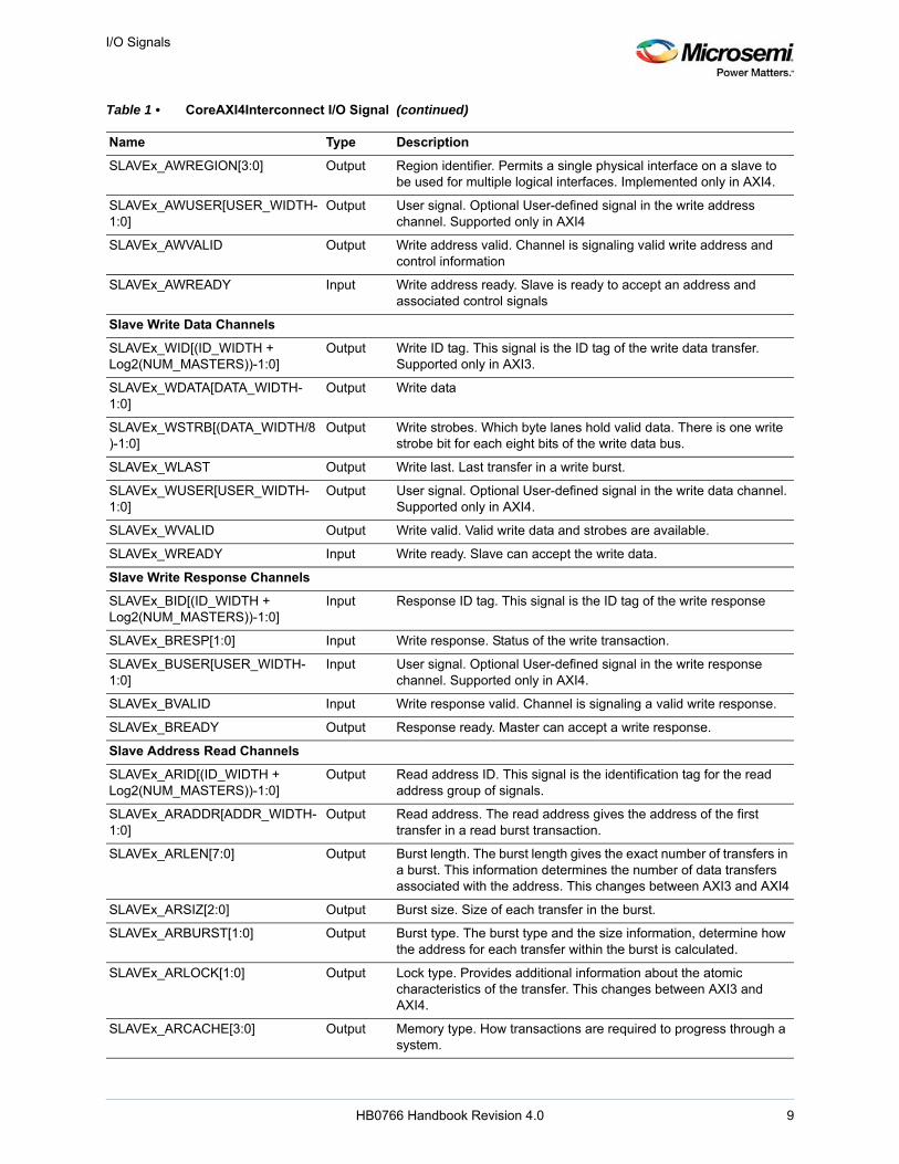
I/O Signals
SLAVEx_AWREGION[3:0] Output Region identifier. Permits a single physical interface on a slave to be used for multiple logical interfaces. Implemented only in AXI4.
SLAVEx_AWUSER[USER_WIDTH-1:0]
Output User signal. Optional User-defined signal in the write address channel. Supported only in AXI4
SLAVEx_AWVALID Output Write address valid. Channel is signaling valid write address and control information
SLAVEx_AWREADY Input Write address ready. Slave is ready to accept an address and associated control signals
Slave Write Data Channels
SLAVEx_WID[(ID_WIDTH + Log2(NUM_MASTERS))-1:0]
Output Write ID tag. This signal is the ID tag of the write data transfer. Supported only in AXI3.
SLAVEx_WDATA[DATA_WIDTH-1:0]
Output Write data
SLAVEx_WSTRB[(DATA_WIDTH/8)-1:0]
Output Write strobes. Which byte lanes hold valid data. There is one write strobe bit for each eight bits of the write data bus.
SLAVEx_WLAST Output Write last. Last transfer in a write burst.
SLAVEx_WUSER[USER_WIDTH-1:0]
Output User signal. Optional User-defined signal in the write data channel. Supported only in AXI4.
SLAVEx_WVALID Output Write valid. Valid write data and strobes are available.
SLAVEx_WREADY Input Write ready. Slave can accept the write data.
Slave Write Response Channels
SLAVEx_BID[(ID_WIDTH + Log2(NUM_MASTERS))-1:0]
Input Response ID tag. This signal is the ID tag of the write response
SLAVEx_BRESP[1:0] Input Write response. Status of the write transaction.
SLAVEx_BUSER[USER_WIDTH-1:0]
Input User signal. Optional User-defined signal in the write response channel. Supported only in AXI4.
SLAVEx_BVALID Input Write response valid. Channel is signaling a valid write response.
SLAVEx_BREADY Output Response ready. Master can accept a write response.
Slave Address Read Channels
SLAVEx_ARID[(ID_WIDTH + Log2(NUM_MASTERS))-1:0]
Output Read address ID. This signal is the identification tag for the read address group of signals.
SLAVEx_ARADDR[ADDR_WIDTH-1:0]
Output Read address. The read address gives the address of the first transfer in a read burst transaction.
SLAVEx_ARLEN[7:0] Output Burst length. The burst length gives the exact number of transfers in a burst. This information determines the number of data transfers associated with the address. This changes between AXI3 and AXI4
SLAVEx_ARSIZ[2:0] Output Burst size. Size of each transfer in the burst.
SLAVEx_ARBURST[1:0] Output Burst type. The burst type and the size information, determine how the address for each transfer within the burst is calculated.
SLAVEx_ARLOCK[1:0] Output Lock type. Provides additional information about the atomic characteristics of the transfer. This changes between AXI3 and AXI4.
SLAVEx_ARCACHE[3:0] Output Memory type. How transactions are required to progress through a system.
Table 1 • CoreAXI4Interconnect I/O Signal (continued)
Name Type Description
HB0766 Handbook Revision 4.0 9

I/O Signals
Note: All signals are active High (logic 1) unless otherwise noted.
SLAVEx_ARPROT[2:0] Output Protection type. Privilege and security level of the transaction, and whether the transaction is a data access or an instruction access.
SLAVEx_ARQOS[3:0] Output Quality of Service, QoS. The QoS identifier sent for each read transaction.Implemented only in AXI4.
SLAVEx_ARREGION[3:0] Output Region identifier. Permits a single physical interface on a slave to be used for multiple logical interfaces. Implemented only in AXI4.
SLAVEx_ARUSER[USER_WIDTH-1:0]
Output User signal. Optional User-defined signal in the read address channel. Supported only in AXI4
SLAVEx_ARVALID Output Read address valid. Channel is signaling valid read address and control information
SLAVEx_ARREADY Input Read address ready. Slave is ready to accept an address and associated control signals
Slave Read Data Channels
SLAVEx_RID[(ID_WIDTH + Log2(NUM_MASTERS))-1:0]
Input Read ID tag. This signal is the identification tag for the read data group of signals generated by the slave.
SLAVEx_RDATA[DATA_WIDTH-1:0]
Input Read data
SLAVEx_RRESP[1:0] Input Read response. Status of the read transfer.
SLAVEx_RLAST Input Read last. Last transfer in a read burst.
SLAVEx_RUSER[USER_WIDTH-1:0]
Input User signal. Optional User-defined signal in the read data channel. Supported only in AXI4.
SLAVEx_RVALID Input Read valid. Channel is signaling the required read data.
SLAVEx_RREADY Output Read ready. Master can accept the read data and response information.
Table 1 • CoreAXI4Interconnect I/O Signal (continued)
Name Type Description
HB0766 Handbook Revision 4.0 10

AXI4 Crossbar
4 AXI4 Crossbar
Each instance of the AXI4 Interconnect core contains one AXI4 Crossbar instance, if it is configured with more than one SIave and one Master.
The SP of the AXI4 Crossbar core can be configured to comprise 1 to 32 SP slots to accept transactions from up to 8 connected master ports. The MP can be configured to comprise 1 to 8 MP slots to issue transactions to up to 32 connected slave devices. The AXI4 Cross bar key features are:
• Selectable Crossbar Architecture – crossbar (SAMD) or shared-data access (SASD)• Crossbar mode (Performance optimized)
• Shared-Address (one for Write addresses, one for read addresses), Multiple-Data (SAMD) crossbar architecture.
• Parallel crossbar pathways for Write data and Read data channels. This enables independent and concurrent Write Data transactions on up to 8 write data paths, as well as independent and concurrent Read Data transactions on up to 8 read data paths. This allows multiple data transactions in parallel provided AXI4 ordering rules are met, which the crossbar imposes.
• Allows programmable number of outstanding transaction at a time.• Sparse crossbar datapaths according to configured connectivity map, resulting in reduced
resource utilization.• One shared Write address bus, plus one shared Read address bus.• One shared Response bus.• Arbitration latencies typically do not impact data throughput when transactions average at least
two data beats.• Crossbar always operates with AXI4 master and slaves.• Enhanced frequency of operation can be configured trading off some latency in system for
higher frequency of operation.• Shared Access mode (Area optimized)
• Shared write data, shared read data, and shared write address, shared read-address buses (SASD).
• One shared Response bus.• Minimizes resource utilization.
• Supports connected masters with multiple reordering depths (ID threads).• Supports up to 8-bit wide ID signals with varying ID width per connected master.• Configurable Write and Read transaction acceptance limits for each connected master.• Configurable Write and Read transaction issuing limits for each connected slave.• Optional single-thread mode (per connected master) reduces thread control logic by allowing one or
more outstanding transactions from only one thread ID at a time.• “Single-Slave per ID” method of cyclic dependency (deadlock) avoidance
For each ID thread issued by a connected master, the Crossbar allows one or more outstanding transactions to only one slave device for Writes and one slave device for Reads, at a time.
• Round-robin arbitration• Round-robin arbitration is used among all connected masters.• Any SP slot that has reached its outstanding limit, or is targeting an MP slot that has reached its
issuing limit, or is trying to access an MP slot in a manner that risks deadlock, is temporarily removed from arbitration, so that other SP slots can be granted arbitration.
The AXI4Interconnect core can be put in one of several modes:
4.1 Pass-Through/ConversionIn the case, only one master needs to connect to one slave, the AXI4Interconnect can be put in 1-to-1 or pass-through mode. In this case, the only function of the core is to convert, such as connecting an AXI4 Master to and AXI4/3 Slave. The crossbar is eliminated, hence no arbitration or extra latency or area.
HB0766 Handbook Revision 4.0 11

AXI4 Crossbar
Figure 3 • Pass-Through
4.2 N-to-1 Interconnect or 1-to-M InterconnectA common configuration for the AXI Interconnect core is when multiple master devices arbitrate for access to a single slave device, often a memory controller. In these cases, address decoding logic might be unnecessary and omitted from the AXI Interconnect core (unless address range validation is needed). Pipeline and protocol conversions to/from AXI3 and AXI4Lite are useful.
Another de-generative configuration of the AXI Interconnect core is when a single master device, typically a processor, accesses multiple memory-mapped slave peripherals.
In these cases (N-to-1 and 1-to-M), all use the AXI4Interconnnect arbitration, address decode and data pathways as normal. Generally a SASD is used as parallel access is not possible.
4.3 N-to-M Interconnect (Shared Access Mode)When in Shared Access mode, the N-to-M use case of the AXI Interconnect core provides for only one outstanding read transaction and one outstanding write transaction at a time. The arbiter selects from among the requesting masters. One write data transfer is enabled to the targeted slave device and after the data transfer (including the write response) completes, the next write request is arbitrated. Similarly one read transaction is selected in parallel to a write cycle and performed at the same time. Shared Access mode minimizes the resources used to implement the crossbar module of the AXI4Interconnect.
HB0766 Handbook Revision 4.0 12

AXI4 Crossbar
Figure 4 • N-to-M Interconnect - Shared Access Mode showing 8 × 8 Example
4.4 N-to-M Interconnect (Crossbar Mode)When in Crossbar mode, the N-to-M use case of the AXI Interconnect core provides for parallel data pathways to allow multiple writes and read transactions to be executed at the same time. There are up to thirty-two separate pathways for writes - one for each slave, and up to eight separate pathways for reads - one for each master.
There is one write address pathway, one read address pathway and one response pathway that are shared by all masters and slaves. The sharing of the address and responses pathways does not normally effect performance as long as data bursts are longer than two. All these pathways - write address, read address, write data, read data, and response all operate in parallel.
HB0766 Handbook Revision 4.0 13

AXI4 Crossbar
Figure 5 • N-to-M Interconnect - Crossbar Mode Showing 8 × 8 example
4.5 AXI4Crossbar Limitations• AXI4 QoS signals do not influence crossbar arbitration priority. QoS signals are only propagated
from Masters to Slaves.• The AXI4 Crossbar does not time out if the destination of any AXI channel transfer stalls indefinitely.
All slaves must respond to all received transactions, as required by AXI protocol.• AXI4 Crossbar does not check if burst cross any illegal boundary. The master is required to handle
that.
HB0766 Handbook Revision 4.0 14

Data-Width Converter
HB0766 Handbook Revision 4.0 15
5 Data-Width Converter
The data width Converter functions depend on whether the data path width gets wider (“up-sizing”) or narrower (“down-sizing”) when moving in the direction from the Master port to Slave Port. The data width conversion functions are the same in either the Master or Slave side. At the master side, width conversion is implemented when required to translate from the master to the AXI Interconnect core native width. Similarly at the slave side, conversion is implemented if required when translating from the AXI Interconnect core native width to the Slave.
• Master, Slave, and Crossbar can be any legal AHB/AXI data width from 32 to 512 bits.• When upsizing, write data is packed (merged) where feasible to the full bus width for efficient
external memory access.• When upsizing, both read and write data is buffered for efficient use of burst-type memory such as
DRAM by allowing bursts of full data width accesses once bus arbitration is achieved externally.• When downsizing, burst transactions are split into multiple transactions if the maximum burst length
would otherwise be exceeded.

Master Protocol Converter
HB0766 Handbook Revision 4.0 16
6 Master Protocol Converter
The Master Protocol Converter transforms connected Masters from AXI3, AXI4Lite or AHB-Lite to AXI4, which is the native protocol type of the AXI4Interconnect. Connected Masters that AXI4 are passed-through the module.
The parameter MASTERx_TYPE defines, one per connected Master port, the type of Master that connects to the AXI4Interconnect. X represents the per port version – MASTER0_TYPE. The following table shows the mapping for the MASTERx_TYPE parameter.
Table 2 • Master_Type Mapping
MASTERx_TYPE[1:0] Port Type
00 AXI4
01 AXI4Lite
10 AHB-Lite
11 AXI3

Slave Protocol Converter
HB0766 Handbook Revision 4.0 17
7 Slave Protocol Converter
The Slave Protocol Converter transforms the native AXI4 ports for connected Slaves to AXI3 or AXI4-Lite. Connected Slaves that AXI4 use passed-through the module.
The parameter SLAVEx_TYPE defines, on per connected Slave port, the type of Slave that connects to the AXI4Interconnect. X represents the per port version (e.g. SLAVE0_TYPE). The following table shows the mapping for the SLAVEx_TYPE parameter.
The key mechanisms for AXI4-Lite protocol conversion are:
• The AXI Interconnect stores transaction IDs from Masters and inserts them during response transfers, when connected to an AXI4-Lite slave.
• The AXI4 Interconnect core breaks-up burst transactions of more than 1 data beat from AXI4 or AXI3 masters into multiple transactions of 1 beats when addressed to an AXI4Lite slave.
• INCR, FIXED, and WRAP burst types are supported
The key mechanisms for AXI3 protocol conversion are:
• The AXI Interconnect core converts burst transactions of more than 16 data beats from AXI4 masters into multiple transactions of no more than 16 beats when connected to an AXI3 slave.
• AXI3 write data interleaving not supported. This feature was dropped by AXI4 protocol.• Atomic locked transactions not supported. This feature was dropped by AXI4 protocol.• AXI3/4 read interleaving from slaves is disabled by storing IDs in a FIFO to return them on
responses to the master, while driving zero to the slave ID. Slaves cannot interleave data with the same ID. Hence, interleaving is disabled.
Table 3 • SLAVE_TYPE mapping
SLAVEx_TYPE[1:0] Port Type
00 AXI4
01 AXI4Lite
10 (reserved)
11 AXI3

Utilization and Performance
HB0766 Handbook Revision 4.0 18
8 Utilization and Performance
All Microsemi SmartFusion2 SoC FPGA family and devices are supported. The following tables list a summary of various parameter settings data. The PolarFire MPF300TS_ES-1FCG484E device is used in deriving the following data.
Note: NUM_MASTERS = 8, NUM_SLAVES= 8, DATA_WIDTH = 32, ADDR_WIDTH = 32, ID_WIDTH = 1, OPEN_TRANS_MAX=2, CROSSBAR_MODE=1, SLAVEx_RS-1, MASTER_RSx=1, RD_ARB_EN=0.
Note: NUM_MASTERS = 8, NUM_SLAVES= 8, DATA_WIDTH = 64, ADDR_WIDTH = 32, ID_WIDTH = 1, OPEN_TRANS_MAX=2, CROSSBAR_MODE=1, SLAVEx_RS-1, MASTER_RSx=1, RD_ARB_EN=0.
Note: NUM_MASTERS = 8, NUM_SLAVES= 8, DATA_WIDTH=64, MASTER0_DATA_WIDTH = 32 (all other masters 64), SLAVE1_DATA_WIDTH=32 (all other slaves 64), ADDR_WIDTH = 32, ID_WIDTH = 1, OPEN_TRANS_MAX=2, CROSSBAR_MODE=1, SLAVEx_RS-1, MASTER_RSx=1, RD_ARB_EN=0; all ports AXI4.
Table 4 • CoreAXI4Interconnect Device Utilization and Performance (8 × 8, Crossbar only, 32-Bit)
Resources 4LUTs DFF Logic Elements Performance MHz
Number used 7429 11368 14900 228 MHz
% Utilization 2.5 3.8 5.0
Table 5 • CoreAXI4Interconnect Device Utilization and Performance (8 × 8, Crossbar only, 64-Bit)
Resources 4LUTs DFF Logic Elements Performance MHz
Number used 15986 12769 20247 202 MHz
% Utilization 2.5 3.8 5.0
Table 6 • CoreAXI4Interconnect Device Utilization and Performance (8 × 8, 64-Bit Crossbar and Converters)
Resources 4LUTs DFF Logic Elements Performance MHz
Number used 28968 20403 34367 180 MHz
% Utilization 9.7 6.8 11.5

Reference Documents
HB0766 Handbook Revision 4.0 19
9 Reference Documents
The following table shows the list of documents referred in this document.
Table 7 • Reference Documents
Document ID Document Name
[R1] IHI0022E - AMBA AXI and ACE Protocol Specification
[R2] ARM_IHI0033A_AMBA_AHB-Lite_SPEC.pdf

Design Description
10 Design Description
10.1 ParametersThe following table describes the CoreAXI4Interconnect parameters for configuring the RTL code. All parameters and generics are integer types.
Table 8 • CoreAXI4Interconnect Parameters or Generics Descriptions
Parameter Name Valid Values Default Description
NUM_MASTERS 1 to 8 8 Number of connected masters to be supported by the crossbar.
NUM_SLAVES 1 to 32 8 Number of connected slaves to be supported by the crossbar.
ID_WIDTH 1 to 8 1 Number of identification tag bits to be supported for each port.It is same for all masters and slaves.Slave ID bits have master infrastructure number pre-pended to ID bits. The slave port ID bits wider than master by number of bits to define NUM_MASTER number.
DATA_WIDTH 32, 64, 128, 256, 512
32 Data width for the core, Crossbar, and other components.
ADDR_WIDTH 16 to 64 20 Number of bits in the Address.
USER_WIDTH 1-8 1 Number of bits for USER signals RUSER and WUSER.
DWC_ADDR_FIFO_DEPTH_CEILING 4 to 32 10 DWC Address FIFO Depth Ceiling is used to bound the size of the command FIFOs in the data width converter. It is a general parameter that the user can set to have small command FIFOs if they run out of resources.
NUM_THREADS 1-4 1 Number of independent threads per master supported.
OPEN_TRANS_MAX 1-8 2 Maximum number of outstanding transactions per thread per Master, that is, transaction acceptance limits for reads and writes. Used for both reads and writes, separate counts are used.
UPPER_COMPARE_BIT 10 - ADDR_WIDTH
15 Upper bit of range to compare.
LOWER_COMPARE_BIT 10-ADDR_WIDTH
12 Lower bound of compare - bits below are don't care for address decode (considered part of that slave's valid memory space).
SLV_AXI4PRT_ADDRDEPTH 2-8 4 Depth of internal FIFO to hold Address for bursts when converting to AXI3 or AXI4Lite. Used to decouple Master from Slave side when burst translation needed (breaking AXI4 burst to multiple smaller bursts) for reads and writes.
HB0766 Handbook Revision 4.0 20

Design Description
SLV_AXI4PRT_DATADEPTH 2-9 4 Depth of internal FIFO to hold Data for bursts when converting to AXI3 or AXI4Lite. Used to decouple Master from Slave side when burst translation needed (breaking AXI4 burst to multiple smaller bursts) for reads and writes.
CROSSBAR_MODE 0 or 1 1 Indicates if crossbar is SAMD or SASD. SAMD is performance-optimised option with Shared-Address paths but with multiple data paths. SASD is the area optimised options with shared address paths with shared data paths. When set to '1', configuration is for full non-blocking data path. When set to '0', configuration is for shared access data path crossbar.
RD_ARB_EN 0 or 1 0 Read Arbitration Enable. RD_ARB_EN defines the way Read Data transactions are handled. When RD_ARB_EN is not asserted, Read Data cycles are handled in an ordered manner on a per port basis (in order they were issued). When RD_ARB_EN is asserted, a round-robin arbitrator is used to select next slave to read from based on RVALIDs asserted.
MASTERx_TYPE[1:0] (where, x is 0 through 7)
2'b00, 2'b01,2'b10, 2'b11
2'b00 Type of interface for the master port. Valid values are:2'b00 - AXI4 master2'b01 - AXI4-Lite master2'b10 - AHB-Lite master2'b11 - AXI3 master
MASTERx_DATA_WIDTH (where, x is 0 through 7)
32, 64, 128, 256, 512
DATA_WIDTH
Data widths of master ports: If master data width < DATA_WIDTH, the master data converter up-scales. If master data width > DATA_WIDTH, the master data converter down-scales.If master data width = DATA_WIDTH, no data-width conversion so master data converter is in pass-through mode.AXI4-Lite masters are limited by protocol to DATA_WIDTHs of 32 and 64.
MASTERx_DWC_DATA_FIFO_DEPTH (where, x is 0 through 7)
16, 32, 64 16 Internal FIFO depth for width converters at the master side. The width of each buffer entry is the width of the master.
MASTERx_CHAN_RS (where, x is 0 through 7)
0 or 1 1 Defines whether a full Register Slice is added to Master Address Write/Read bus, Master Write/Read Data bus and Master Write Response bus.
Adding a register slice can increase maximum frequency of operation at the cost of extra latency cycles.
MASTERx_CLOCK_DOMAIN_CROSSING
0 or 1 0 When high, a clock-domain crossing core is instantiated at the master port or at the internal side of a master protocol converter.
Table 8 • CoreAXI4Interconnect Parameters or Generics Descriptions (continued)
Parameter Name Valid Values Default Description
HB0766 Handbook Revision 4.0 21

Design Description
SLAVEy_TYPE[1:0] (where, y is 0 through 31)
2'b00, 2'b01, 2'b11 (2'b10 is reserved)
2'b00 Type of interface for the slave port. Valid values are:2'b00 - AXI4 slave2'b01 - AXI4-Lite slave2'b11 - AXI3 slave
SLAVEy_DATA_WIDTH (where y is 0 through 31)
32, 64, 128, 256, 512
DATA_WIDTH
Data widths of slave ports:If slave data width < DATA_WIDTH the slave data converter down-scales.If slave data width > DATA_WIDTH the slave data converter up-scales.If slave data width = DATA_WIDTH no data-width conversion so slave data converter is in pass-through mode.AXI4-Lite slaves are limited by protocol to DATA_WIDTHs of 32 and 64.
SLAVEy_DWC_DATA_FIFO_DEPTH (where, y is 0 through 31)
16, 32, 64 16 Internal FIFO depth for width converters at the slave side. The width of each buffer entry is the width of the slave.
SLAVEy_CLOCK_DOMAIN_CROSSING
0 or 1 0 When high, a clock-domain crossing core is instantiated at the slave port or at the internal side of a slave protocol converter.
SLAVEy_CHAN_RS (where, y is 0 through 8)
0 or 1 1 Defines whether a full Register Slice is added to Slave Address Write/Read bus, Slave Write/Read Data bus and Slave Write Response bus
Adding a register slice can increase maximum frequency of operation at the cost of extra latency cycles.
SLOTy_BASE_VEC [(ADDR_WIDTH-UPPER_COMPARE_BIT)-1 : 0] (where, y is 0 through 31)
0 to 31 - Base Address for each slave.
SLOTy_MIN_VEC [ (UPPER_COMPARE_BIT-LOWER_COMPARE_BIT))-1 : 0] (where, y is 0 through 31)
0 to 0xFFFFFFFF
- Lowest address for each slave.
SLOTy_MAX_VEC [ (UPPER_COMPARE_BIT-LOWER_COMPARE_BIT))-1 : 0] (where, y is 0 through 31)
0 to 0xFFFFFFFF
- Highest address for each slave.
MASTERx_WRITE_SLAVEy (where,"x is 0 … 7 i.e. one per master port"y is 0 … 31 i.e. one per slave port)
0 or 1 1 Bit per master per slave indicating if a master can write to a slave port. Used to "trim" internal decode/arbitration logic for Masters that cannot write to a specific slave.
MASTERx_READ_SLAVEy(where,"x is 0 … 7 i.e. one per master port"y is 0 … 31 i.e. one per slave port)
0 or 1 1 Bit per master per slave. Used to "trim" internal decode/arbitration logic for Masters that cannot read from a specific slave.
Table 8 • CoreAXI4Interconnect Parameters or Generics Descriptions (continued)
Parameter Name Valid Values Default Description
HB0766 Handbook Revision 4.0 22

Design Description
MASTERx_DEF_BURST_LEN (where x is 0 through 7)
0 to 255 0 Default burst length of AXI transactions created by the AHB converter. Used for undefined AHB burst type (INCR). For applications where, AXI bursts are an advantage, such as DRAM accesses, this may be set to 15 for example for 16-beat bursts. If AHB undefined length bursts finish early, AXI transactions are completed as required by the AXI specification, with writes not asserting write strobes on the additional beats. If AHB transactions continue beyond this value, new additional AHB transactions will be created.
AHB_MASTERx_BRESP_CHECK_MODE (where, x is 0 through 7)
2'b00, 2'b10, 2'b11(2'b01 is reserved)
2'b00 Defines how the AHB master converter should handle the BRESP[1:0] signals form the AXI side:2'b0x - ignores BRESP: lowest latency2'b10 - checks at the end of every AHB burst; medium latency2'b11 - checks at the end of every AXI burst: highest latency
Table 8 • CoreAXI4Interconnect Parameters or Generics Descriptions (continued)
Parameter Name Valid Values Default Description
HB0766 Handbook Revision 4.0 23

Design Details
11 Design Details
11.1 System OverviewThe CoreAXI4Interconnect provides the interconnection between one and eight of AXI4, AXI3, AHBLite, and AXI4Lite to between one and eight AXI4, AXI3, and AXI4Lite Slaves. It is composed of three main components—a Master_Converter (one per master port), a AXI4CrossBar, and a Slave_Converter (one per slave port). The following figure shows a high-level block diagram for the core.
Figure 6 • CoreAXI4Interconnect
The core operates using the AXI4 protocol internally. It is only at the ingress to Master Converter and egress of Slave_Converter is AXI3 or AXI4Lite protocol handled. The following sections provide a high-level description of these three components.
11.2 Write CyclesThe AXI4Interconnect, with no converters, normally adds a latency of 2 ACLK ticks from the Master asserting AWVALID and the target Slave device seeing AWVALID asserted as shown in the following figure. The AWREADY is asserted with no extra latency to the Master when the Slave asserts it. The two latency cycles are required for the address arbitrator to see signal asserted and then to make a decision on which master goes next. If this Master is not next based on the round-robin scheme, it may have to wait additional cycles until it is its turn.
HB0766 Handbook Revision 4.0 24

Design Details
Figure 7 • Address Latency
When a register slice is enabled on MASTER_AWCHAN (that is, when MASTER_AWCHAN_RS=1), it adds another latency cycle to AWVALID being asserted to the target slave as shown in the following figure. Also AWREADY is normally asserted to Master as the RegSlice "consumes" the cycle.
Figure 8 • Address Latency when AWCHAN RegSlice is enabled
When a Register Slice is enabled on slave AWCHAN (that is, SLAVE_AWCHAN_RS=1), another latency cycle is added to the delay in AWVALID path from master to slave.
HB0766 Handbook Revision 4.0 25

Design Details
A typical write cycle is shown in the following figure. In this example, register slices are not enabled.
Figure 9 • Write Cycle
HB0766 Handbook Revision 4.0 26

Design Details
11.3 Read CyclesThe AXI4Interconnect read address without converters is similar to write address cycles. In general, a latency of two ACLK ticks from the Master asserting ARVALID and the target Slave device seeing ARVALID asserted. The ARREADY is asserted with no extra latency to the Master when the Slave asserts it. The two latency cycles are required for the address arbitrator to see signal asserted and then to make a decision on which master goes next. If this Master is not next based on the round-robin scheme, it may have to wait additional cycles until it is its turn.
The following figure shows an example of a Read Cycle. In this example, Register Slice are not enabled.
Figure 10 • Read Cycle
HB0766 Handbook Revision 4.0 27

Design Details
11.4 Address DecodingThe AXI4Interconnect decodes the ARADDR and AWADDR in the AXI4Crossbar module to select which SLAVE port the MASTER wants to burst to. This decode is performed using the following equation:
MATCHy SLAVE = Addr[ADDR_WIDTH-1:UPPER_COMPARE_BIT] == SLOTy_BASE_ADDR)
and
(Addr[UPPER_COMPARE_BIT-1:LOWER_COMPARE_BIT] >= SLOTy_MIN_ADDR)
and
(Addr[UPPER_COMPARE_BIT-1:LOWER_COMPARE_BIT] <= SLOTy_MAX_ADDR);
Where:
• y is 0 to NUM_SLAVES, refers to port number• MATCHy SLAVE is the target port for the transaction. There is one MATCH SLAVE per port, where a
maximum of one SLAVE port is matched in a properly configured system.• Addr is the ARADDR or AWDDR for the transaction.• UPPER_COMPARE_BIT is per core parameter that defines width of SLOT_BASE_ADDR (through
ADDR_WIDTH - UPPER_COMPARE_BIT).• LOWER_COMPARE_BIT is per core parameter that defines width of SLOT_MIN_ADDR and
SLOT_MAX_ADDR parameters (through UPPER_COMPARE_BIT - LOWER_COMPARE_BIT).• SLOTx_BASE_ADDR is the base address for the associate SLAVEx port.• SLOTx_MIN_ADDR is the minimum address for the associate SLAVEx port.• SLOTx_MAX_ADDR is the maximum address for the associate SLAVEx port.
11.4.1 Address Decode Example 1For this example, the core's address parameters are defined as follows:
ADDR_WIDTH = 32;
UPPER_COMPARE_BIT = 28;
LOWER_COMPARE_BIT = 24;
NUM_SLAVES = 8;
SLOT7_BASE_VEC = { 4'h7 };// base for SLAVE7
SLOT6_BASE_VEC = { 4'h6 };// base for SLAVE6
SLOT5_BASE_VEC = { 4'h5 };// base for SLAVE5
SLOT4_BASE_VEC = { 4'h4 };// base for SLAVE4
SLOT3_BASE_VEC = { 4'h3 };// base for SLAVE3
SLOT2_BASE_VEC = { 4'h2 };// base for SLAVE2
SLOT1_BASE_VEC = { 4'h1 };// base for SLAVE1
SLOT0_BASE_VEC = { 4'h0 };// base for SLAVE0
SLOT7_MIN_VEC ={ 4'b0000 };// base for SLAVE7
SLOT6_MIN_VEC ={ 4'b0000 };// base for SLAVE6
SLOT5_MIN_VEC ={ 4'b0000 };// base for SLAVE5
SLOT4_MIN_VEC ={ 4'b0010 };// base for SLAVE4
SLOT3_MIN_VEC ={ 4'b0000 };// base for SLAVE3
SLOT2_MIN_VEC ={ 4'b0001 };// base for SLAVE2
SLOT1_MIN_VEC ={ 4'b0000 };// base for SLAVE1
HB0766 Handbook Revision 4.0 28
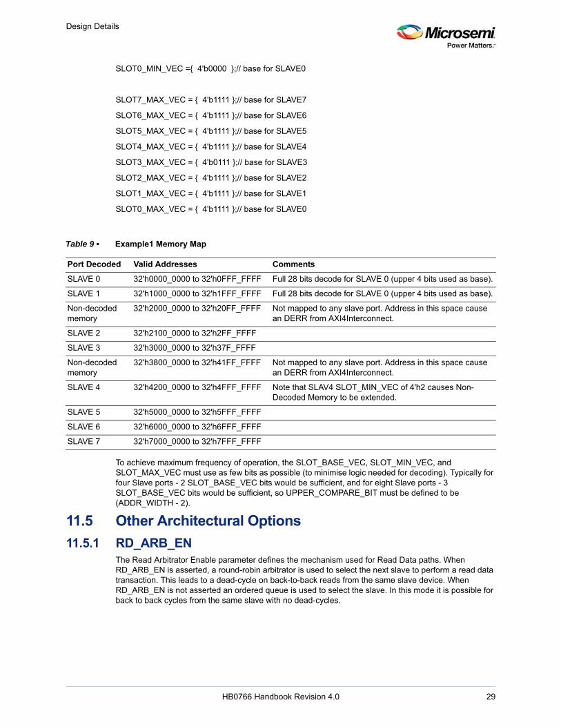
Design Details
SLOT0_MIN_VEC ={ 4'b0000 };// base for SLAVE0
SLOT7_MAX_VEC = { 4'b1111 };// base for SLAVE7
SLOT6_MAX_VEC = { 4'b1111 };// base for SLAVE6
SLOT5_MAX_VEC = { 4'b1111 };// base for SLAVE5
SLOT4_MAX_VEC = { 4'b1111 };// base for SLAVE4
SLOT3_MAX_VEC = { 4'b0111 };// base for SLAVE3
SLOT2_MAX_VEC = { 4'b1111 };// base for SLAVE2
SLOT1_MAX_VEC = { 4'b1111 };// base for SLAVE1
SLOT0_MAX_VEC = { 4'b1111 };// base for SLAVE0
To achieve maximum frequency of operation, the SLOT_BASE_VEC, SLOT_MIN_VEC, and SLOT_MAX_VEC must use as few bits as possible (to minimise logic needed for decoding). Typically for four Slave ports - 2 SLOT_BASE_VEC bits would be sufficient, and for eight Slave ports - 3 SLOT_BASE_VEC bits would be sufficient, so UPPER_COMPARE_BIT must be defined to be (ADDR_WIDTH - 2).
11.5 Other Architectural Options
11.5.1 RD_ARB_ENThe Read Arbitrator Enable parameter defines the mechanism used for Read Data paths. When RD_ARB_EN is asserted, a round-robin arbitrator is used to select the next slave to perform a read data transaction. This leads to a dead-cycle on back-to-back reads from the same slave device. When RD_ARB_EN is not asserted an ordered queue is used to select the slave. In this mode it is possible for back to back cycles from the same slave with no dead-cycles.
Table 9 • Example1 Memory Map
Port Decoded Valid Addresses Comments
SLAVE 0 32'h0000_0000 to 32'h0FFF_FFFF Full 28 bits decode for SLAVE 0 (upper 4 bits used as base).
SLAVE 1 32'h1000_0000 to 32'h1FFF_FFFF Full 28 bits decode for SLAVE 0 (upper 4 bits used as base).
Non-decoded memory
32'h2000_0000 to 32'h20FF_FFFF Not mapped to any slave port. Address in this space cause an DERR from AXI4Interconnect.
SLAVE 2 32'h2100_0000 to 32'h2FF_FFFF
SLAVE 3 32'h3000_0000 to 32'h37F_FFFF
Non-decoded memory
32'h3800_0000 to 32'h41FF_FFFF Not mapped to any slave port. Address in this space cause an DERR from AXI4Interconnect.
SLAVE 4 32'h4200_0000 to 32'h4FFF_FFFF Note that SLAV4 SLOT_MIN_VEC of 4'h2 causes Non-Decoded Memory to be extended.
SLAVE 5 32'h5000_0000 to 32'h5FFF_FFFF
SLAVE 6 32'h6000_0000 to 32'h6FFF_FFFF
SLAVE 7 32'h7000_0000 to 32'h7FFF_FFFF
HB0766 Handbook Revision 4.0 29

Design Details
11.5.2 HI_FREQThe High Frequency (HI_FREQ) parameter is used to increase the maximum possible frequency of operation. The cost for this is extra latency cycles. An additional cycle is added to the Address paths - Address Write and Address Read, as well as another on the RESP paths. The following figure shows how HI_FREQ changes write transactions compared to standard Write transactions (that is HI_FREQ=0).
Figure 11 • Write Cycle with HI_FREQ asserted
11.5.3 Connectivity MatrixThe MASTERx_WRITE_SLAVEy and MASTERx_READ_SLAVEy parameters are used to prune the decode and arbitration logic. Each master has a bit per slave that defines whether that master can write to that slave (MASTERx_WRITE_SLAVEy, where x is 0 to 7 referring to MASTER0 to MASTER7) and another bit per slave that defines whether that master can read from that slave (MASTERx_READ_SLAVEy). MASTERx_WRITE_CONNECTIVITY is a concatenation of {MASTERx_WRITE_SLAVE7 …. MASTERx_WRITE_SLAVE0} and MASTERx_READ_CONNECTIVITY is a concatenation of {MASTERx_READ_SLAVE7 …. MASTERx_READ_SLAVE0}.
HB0766 Handbook Revision 4.0 30

Design Details
These matrices are used to remove slaves that have their connectivity bit set to zero from arbitration and other logic. The following figure shows an example of how the MASTER_WRITE_CONNECTIVITY is used. MASTER_READ_CONNECTIVITY is defined in a similar manner.
Figure 12 • MASTER_WRITE_CONNECTIVITY Example
11.5.4 AXI3 and AXI4Lite Slave ConfigurationA connected AXI3 or AXI4Lite Slave can be supported by configuring SLAVE_TYPE for that port. The parameters SLV_AXI4PRT_ADDRDEPTH and SLV_AXI4PRT_DATADEPTH are used to configure how much storage is used to hold address transactions and data transactions. Typically both are set to 3 which means that storage of a depth of 23 or 8 will be provided to hold transactions between internal AXI4 bus and external AXI3. Typically SLV_AXI4PRT_ADDRDEPTH should be the same value as OPEN_TRANS_MAX to avoid holding up address transactions and SLV_AXI4PRT_DATADEPTH of 3 which provides storage of depth of 23 or 8 to "buffer" Write/Read data between AXI3 slave and the internal AXI4 bus.
The following figure shows an example of a write of LEN = 17 (that is, 18 beats) from Master 0 to Slave 0. On the SLAVE0 connections this burst is broken into two - one of LEN=15 (16 beats) and a second of LEN=1 (two beats). These two bursts RESPONSES are combined into one to send back to MASTER0. On this example no errors are indicated in the response. In cases where an error is indicated in BRESP, all responses are combined. The BRESP returned to the connected master is set to the first error response received from the connected slave.
HB0766 Handbook Revision 4.0 31

Design Details
Figure 13 • AXI3 Write Example
A port configured as AXI4Lite (SLAVE_TYPE set to 2'b10 for that port) will operate similar to what is shown in the preceding figure except that all Slave side LEN will be 0. The AXI4Interconnect will store a transactions' AWID/WID/ARID/RID/BID as necessary to label each transaction correctly for the Master.
As with the width converters, the SLAVE ID is always sent out as "zero" to prevent read interleaving problems. Instead the Master ID is stored in a FIFO and returned to the master intact.
11.5.5 AHB to AXI4 Master ConversionA connected AHB master (MASTER_TYPE = 10) will convert the AHB protocol to AXI4. The differences between protocols are as follows:
• AXI has five independent channels (write and read address/control, write and read data, and write response) whereas AHB has one.
• AXI has an undefined length burst type, INCR, with no way to predict when it will end until a new transaction starts or the bus goes idle; AXI specifies the length of transactions at the start.
• AXI and AHB have "response" indications for error conditions, but they are handled very differently: AHB is on per-beat basis within a burst for both reads and writes, whereas AXI's response comes once at the end of a burst for reads, and independently later for writes.
• AHB has only one shared "ready" signal for address/control and both read and write data, whereas AXI has a "ready" signal on each of the five channels, along with associated "valid" signals.
HB0766 Handbook Revision 4.0 32

Design Details
The AXI converter handles these as follows.
During back to back transactions without "busy" beats, the last data beat coincides with the next control beat, and "HREADY" is not asserted until both that data is accepted by AXI (AXI RVALID for reads or WREADY for writes) AND the required read or write control channel is ready (AWREADY or ARREADY).
A parameter "MASTERx_DEF_BURST_LEN" is provided to help optimise the AHB performance in an AXI system when bursts are beneficial and the master (for example a CPU) makes wishes to make use of INCR transactions. As an example, when accessing DRAM, a CPU may request access (write or read) to a multi-port arbiter DRAM based on asserting AxVALID, and once successful it may be provided access for the duration of a burst, for example MASTERx_DEF_BURST_LEN =16 beats. This suits DRAM controllers as DRAM access is most efficient when sequential data is written to a DRAM bank. On the positive side, when AHB INCR burst lengths match MASTERx_DEF_BURST_LEN (or multiples of it) this efficiency is achieved. On the other hand if INCR transactions tend to be much lower than this setting, dummy AXI beats are implemented to meet the AXI specification where bursts can't be aborted. On AXI the length of a transaction is specified before the data phase, but this is not known a priori from AHB for INCR's.
On AHB, read responses are provided with the data to indicate errored data, whereas on AXI they're applied only on the last beat while RLAST is asserted. The AHB converter handles this by aborting the AHB transfer with an error sequence once an AXI burst is complete, if the AHB transfer is longer than the default AXI transfer length. If the AHB burst size is not a multiple of the AXI burst length, the last AHB data beat is held up until the AI transfer is completed and if an AXI errored response is detected, an error sequence is executed instead of a successful last beat.
Note: In all these cases, the data beat on which the error is indicated is not necessarily erroneous: an error occurring on any beat is indicated on the last beat of an AXI burst. It should be considered to be an overall read transaction error. Parameters do provide the ability to validate each beat of an AHB INCR burst if it's important enough, by assigning MASTERx_DEF_BURST_LEN = 0 (one-beat AXI transfers), and also AHB_MASTERx_BRESP_CHECK_MODE[1] = 1 (checks RRESP at the end of each AXI burst).
Regarding write responses on AHB, the specification requires that HRESP is flagged on a per beat basis. AXI returns write responses independently from the data on the BRESP channel. This may well occur significantly later than the data transfer. If each beat of a transfer had to await BRESP, performance would be significantly impacted. Again, parameters are available to provide the ability to do this if required though with significant performance impact, by assigning MASTERx_DEF_BURST_LEN = 0 and AHB_MASTERx_BRESP_CHECK_MODE = 2'b11.
A medium performance impact option is also available for writes: if for example MASTERx_DEF_BURST_LEN = 15 and AHB_MASTERx_BRESP_CHECK_MODE = 2'b10, for long AHB INCR bursts such as 1024, BRESP error responses are accumulated off-line from the main control functions as each AXI burst of 16 beats completes and returns a BRESP. Only when all 1024 AHB data is written does the control function wait until the last BVALID arrives before allowing the AHB transaction to complete, with or without an error sequence. It tracks BVALID with the aid of a counter which has a width of AHB_MASTER0_BRESP_CNT_WIDTH. For this example (1024-beat AHB converted to 64 sixteen-beat AXI bursts), the counter would reach 64, so a response counter width of 7 would be needed.
The highest performance option is to set AHB_MASTERx_BRESP_CHECK_MODE = 2'b00. This avoids the AHB converter to not wait for the write response. This maximizes performance, but an issue would arise if for example data is read immediately after being written by the same master: if AXI write channels were slow (control or data) but read channels are fast, the read could arrive at the slave before the write is done. AXI systems have the ability to overcome this by using the B channel, but AHB has no such facility. Setting AHB_MASTERx_BRESP_CHECK_MODE[1] to 1 overcomes this.
HB0766 Handbook Revision 4.0 33

Licensing
HB0766 Handbook Revision 4.0 34
12 Licensing
The CoreAXI4Interconnect does not require any license.
12.1 RTLComplete RTL source code is provided for the core and testbenches.

Simulation Flows
HB0766 Handbook Revision 4.0 35
13 Simulation Flows
The User Testbench for AXI4Interconnect is included in all releases.
To run simulations, select the User Testbench flow from SmartDesign and click Save and click Generate on the Generate pane. When SmartDesign generates the Libero SoC project, it installs the user testbench files.
To run the user testbench, set the design route to the CoreAXI4Interconnect instantiation in the Libero SoC design hierarchy pane, right-click Simulate in the Libero SoC Design Flow window under Verify Pre-Synthesized Design and select Open Interactively. This invokes ModelSim and automatically runs the simulation.
13.1 User TestbenchThe following figure shows the user simulation testbench and it includes the instantiation of the CoreAXI4Interconnect macro and multiple AXI4MasterGen and AXI4SlaveGen blocks. The AXI4MasterGen block is a primitive model of an AXI master, which perform writes and reads when initiated by rdStart and wrStart signals within the testbench. The AXI4SlaveGen block is a primitive model of a AXI slave with embedded storage for read/writes.
The user tests are executed in tasks in the testbench. These tasks can be edited.
Figure 14 • CoreAXI4Interconnect User Testbench showing 8 × 8 Example

Synthesis in Libero SoC
HB0766 Handbook Revision 4.0 36
14 Synthesis in Libero SoC
After setting the design root appropriately for the design, use the following steps to run the Synthesis:
1. Click Synthesis in the Libero SoC software. The Synthesis window appears displaying the Synplicity project.
2. Set Synplicity to use the Verilog 2001 standard if Verilog is used. 3. Click Run to run the Synthesis.

Place-and-Route in Libero SoC
HB0766 Revision 4.0 37
15 Place-and-Route in Libero SoC
After setting the design route appropriately for the design, and running Synthesis, click Layout in the Libero SoC software to invoke Designer. CoreAXI4Interconnect does not require special place-and-route settings.