logic families - bubu.edu.eg/portal/uploads/engineering, shoubra/electrical... · –cmos...
TRANSCRIPT
Logic Families
Dr. Basem Elhalawany

A bit of history
• The first transistors were fabricated in 1947 at Bell Laboratories (Bell Labs) by Brattain with Bardeen providing the theoretical background and Shockley managed the activity. – The trio received a Nobel Prize in Physics for their
work in 1956. • The transistor was called a
point-contact transistor and was
a type of bipolar junction transistor
(BJT).

A bit more history
• The theory on field effect transistors (FETs) was developed much earlier than our understanding of BJTs – First patent on FETs dates from 1925
• Julius Edgar Lilienfeld, an Austro-Hungarian physicist
• However, the quality of the semiconductor and the oxide materials were barriers to developing good working devices. – The first FET was not invented until 1959
• Dawon Kahng and Martin M. (John) Atalla of Bell Labs

Integrated Circuits
• Integrated circuits (ICs) are chips, pieces of semiconductor material, that contain all of the transistors, resistors, and capacitors necessary to create a digital circuit or system.
– The first ICs were fabricated using Ge BJTs in 1958.
• Jack Kirby of Texas Instruments, Nobel Prize in 2000
• Robert Noyes of Fairchild Semiconductors fabricated the first Si ICs in 1959.

Integration Levels
– SSI Small scale integration 12 gates/chip
– MSI Medium scale integration 100 gates/chip
– LSI Large scale integration 1K gates/chip
– VLSI Very large scale integration 10K gates/chip
– ULSI Ultra large scale integration 100K gates/chip
5

Moore’s law
• A prediction made by Moore (a co-founder of Intel) in 1965: “… a number of transistors to double every 2 years.”
6

Logic Families Logic Families
• Logic families are sets of chips that may implement different logical functions, but use the same type of transistors and voltage levels for logical levels and for the power supplies.
• These families vary by speed, power consumption, cost, voltage & current levels
• Logic families are sets of chips that may implement different logical functions, but use the same type of transistors and voltage levels for logical levels and for the power supplies.
• These families vary by speed, power consumption, cost, voltage & current levels
• IC digital logic families
– DL (Diode- logic)
– DTL (Diode-transistor logic)
– RTL (Resistor-transistor logic)
– TTL (Transistor -transistor logic)
– ECL (Emitter-coupled logic)
– MOS (Metal-oxide semiconductor)
– CMOS (Complementary Metal-oxide semiconductor)

Digital IC Terminology Digital IC Terminology • Voltage Parameters:
– VIH(min): high-level input voltage, the minimum voltage level required for a logic 1 at an input.
– VIL(max): low-level input voltage
– VOH(min): high-level output voltage
– VOL(max): low-level output voltage
For TTL For TTL
• For proper operation the input voltage levels to a logic must be kept outside the indeterminate range.
• Lower than VIL(max) and higher than VIH(min).
• For proper operation the input voltage levels to a logic must be kept outside the indeterminate range.
• Lower than VIL(max) and higher than VIH(min).
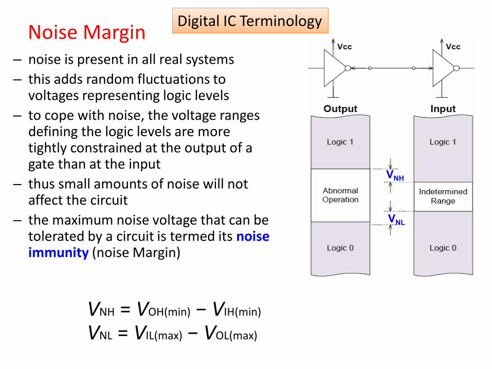
Digital IC Terminology Digital IC Terminology Noise Margin
– noise is present in all real systems
– this adds random fluctuations to voltages representing logic levels
– to cope with noise, the voltage ranges defining the logic levels are more tightly constrained at the output of a gate than at the input
– thus small amounts of noise will not affect the circuit
– the maximum noise voltage that can be tolerated by a circuit is termed its noise immunity (noise Margin)
VNH
VNL
VNH = VOH(min) − VIH(min)
VNL = VIL(max) − VOL(max)

Digital IC Terminology Digital IC Terminology Noise Margin

Current Parameters:
• IOH – Current flowing into an output in the logical “1” state under specified load conditions
• IOL – Current flowing into an output in the logical “0” state under specified load conditions
• IIH – Current flowing into an input when a specified HI level is applied to that input
• IIL – Current flowing into an input when a specified LO level is applied to that input
VOH VIH VOL VIL
IOH IIH IOL IIL
11
Digital IC Terminology Digital IC Terminology

Digital IC Terminology Digital IC Terminology
• The maximum number of standard logic inputs that an output can drive reliably.
• Also known as the loading factor. • Related to the current parameters (both in high and low states.)
fanout
DC fanout = min( )
12
IL
OL
IH
OH
I
I
I
I,

Digital IC Terminology Digital IC Terminology
• Timing considerations
– all gates have a certain propagation delay time, tPD
– this is the average of the two switching times
)t(tt PLHPHLPD 21

Digital IC Terminology Digital IC Terminology
Power Requirements
• Every IC needs a certain amount of electrical power to operate.
• Vcc (TTL)
• VDD(MOS)
• Power dissipation determined by Icc and Vcc.
• Average Icc(avg)= (ICCH + ICCL)/2
• PD(avg) = Icc(avg) x Vcc

Digital IC Terminology Digital IC Terminology
Speed-Power Product
• Desirable properties:
– Short propagation delays (high speed)
– Low power dissipation
• Speed-power product measures the combined effect.
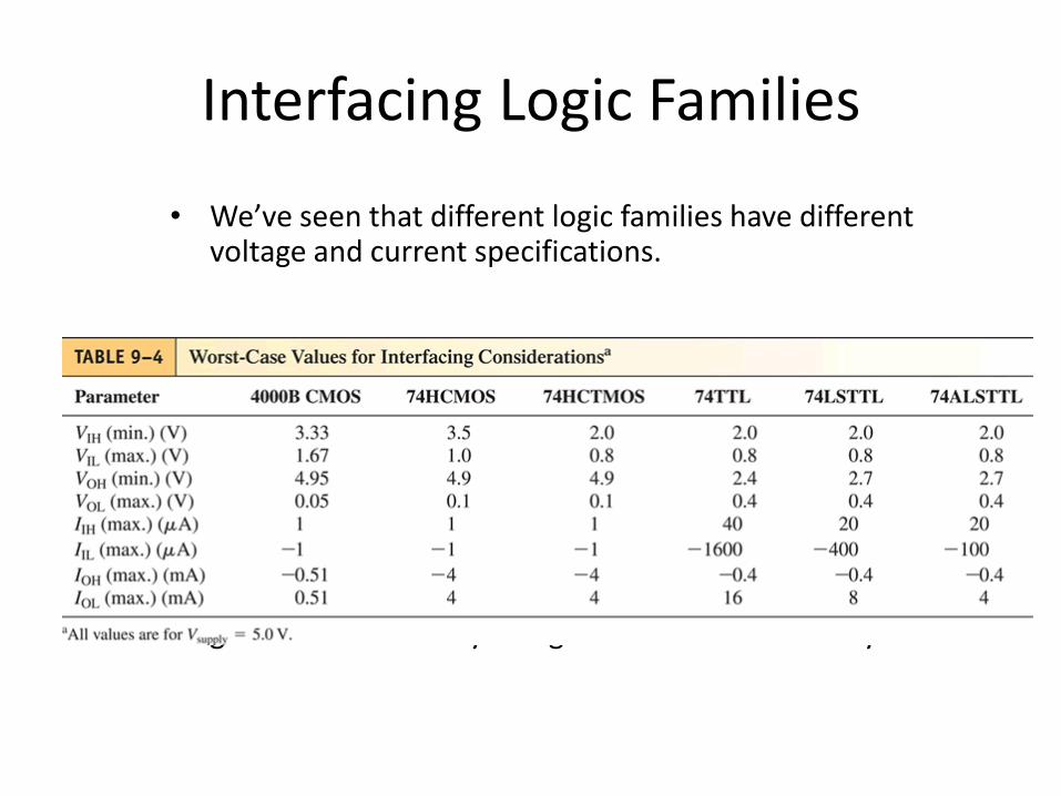
Interfacing Logic Families
• We’ve seen that different logic families have different voltage and current specifications.
• These differences can cause problems when you connect a gate from one family to a gate from another family.

Voltage-Related Interfacing Problems • In some interfacing situations, a HIGH output pin may produce a
voltage that is too low to be recognized as a HIGH by the input pin it’s connected to.
• The solution in such cases is to use a pull-up resistor
• Example: TTL to CMOS
A TTL HIGH output may be as low as 2.4 V.
But a CMOS input expects HIGHs to be at least 3.33 V.

Current-Related Interfacing Problems • In some interfacing situations, either a HIGH output pin may not
source enough current to drive the input pin it’s connected to, or a LOW output pin may not sink enough current to drive the input pin it’s connected to.
• The solution in such cases is to use a buffer. • Example: CMOS to TTL
• A CMOS LOW output can only sink 0.51 mA.
• But as much as 1.6 mA may flow out of a TTL LOW input.
• It can also be used for increasing the fanout
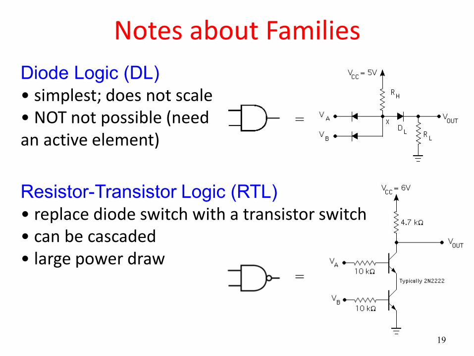
Notes about Families
Diode Logic (DL) • simplest; does not scale • NOT not possible (need an active element)
=
=
Resistor-Transistor Logic (RTL) • replace diode switch with a transistor switch • can be cascaded • large power draw
19

Then
=
Diode-Transistor Logic (DTL) • essentially diode logic with transistor amplification • reduced power consumption • faster than RTL
DL AND gate Saturating inverter
20

TTL Logic Families • TTL: Transistor-Transistor Logic
first introduced by in 1964 (Texas Instruments)
TTL has shaped digital technology in many ways
one of the most widely used families for small- and medium-scale devices – rarely used for VLSI
Standard TTL family (e.g. 7400) is obsolete
Newer TTL families still used (e.g. 74ALS00)
High energy consumption, but
relatively insensitive to electrostatic discharge (ESD)
Distinct features: (Multi-emitter transistors - Totem-pole output)

TTL family evolution
Legacy: don’t use
in new designs
Widely used today
22

ECL
Emitter-Coupled Logic (ECL) • based on BJT, but removes problems of delay time by preventing
the transistors from saturating • very fast operation - propagation delays of 1ns or less • high power consumption, perhaps 60 mW/gate • Logic levels. “0”: –1.7V. “1”: –0.8V • Such strange logic levels require extra effort when interfacing to
TTL/CMOS logic families. • low noise immunity of about 0.2-0.25 V • used in some high speed specialist applications, but now largely
replaced by high speed CMOS
23

CMOS Complimentary MOS (CMOS)
• Considerably lower energy consumption than TTL and ECL, which has made portable electronics possible.
• most widely used family for large-scale devices • combines high speed with low power consumption • usually operates from a single supply of 5 – 15 V • excellent noise immunity of about 30% of supply voltage • can be connected to a large number of gates (about 50)
•Things to watch out for: – don’t leave inputs floating (in TTL these will float to HI, in CMOS you get undefined behaviour) – susceptible to electrostatic damage (finger of death)
24

CMOS/TTL power requirements • TTL power essentially constant (no frequency dependence) • CMOS power scales as f C V2 • At high frequencies (>> MHz) CMOS dissipates more power than TTL • Overall advantage is still for CMOS even for very fast chips – only a relatively small portion of complicated circuitry operates at highest frequencies
frequency supply volt.
eff. capacitance
25

CMOS family evolution obsolete
•Power reduction is one of the keys to progressive growth of integration
26
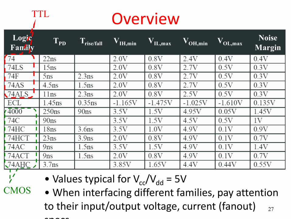
Overview TTL
Logic
Family
CMOS • Values typical for Vcc/Vdd = 5V • When interfacing different families, pay attention to their input/output voltage, current (fanout) specs.
TPD Trise/fall VIH,min VIL,max VOH,min VOL,max Noise
Margin
27

Some Gates
2-input AND Gate Diode-Resistor Logic

Some Gates

Diode-Resistor OR gate

Diode-Resistor AND gate

NOT gate

Common ICs
7400 Quad 2-input Logic NAND Gate Also: 74LS00 Quad 2-input 74LS10 Triple 3-input 74LS20 Dual 4-input 74LS30 Single 8-input
7402 Quad 2-input NOR Gate
7408 Quad 2-input AND Gate 7432 Quad 2-input Logic OR Gate
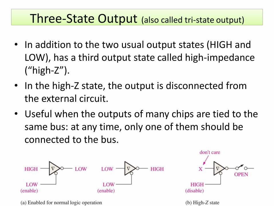
Three-State Output (also called tri-state output) Three-State Output (also called tri-state output)
• In addition to the two usual output states (HIGH and LOW), has a third output state called high-impedance (“high-Z”).
• In the high-Z state, the output is disconnected from the external circuit.
• Useful when the outputs of many chips are tied to the same bus: at any time, only one of them should be connected to the bus.