lmf100 high performance dual switched capacitor filter · lmf100 high performance dual switched...
TRANSCRIPT
LMF100High Performance Dual Switched Capacitor FilterGeneral DescriptionThe LMF100 consists of two independent general purposehigh performance switched capacitor filters. With an externalclock and 2 to 4 resistors, various second-order andfirst-order filtering functions can be realized by each filterblock. Each block has 3 outputs. One output can be config-ured to perform either an allpass, highpass, or notch func-tion. The other two outputs perform bandpass and lowpassfunctions. The center frequency of each filter stage is tunedby using an external clock or a combination of a clock and re-sistor ratio. Up to a 4th-order biquadratic function can be re-alized with a single LMF100. Higher order filters are imple-mented by simply cascading additional packages, and all theclassical filters (such as Butterworth, Bessel, Elliptic, andChebyshev) can be realized.
The LMF100 is fabricated on National Semiconductor’s highperformance analog silicon gate CMOS process,
LMCMOS™. This allows for the production of a very low off-set, high frequency filter building block. The LMF100 ispin-compatible with the industry standard MF10, but pro-vides greatly improved performance.
Featuresn Wide 4V to 15V power supply rangen Operation up to 100 kHzn Low offset voltage: typically
(50:1 or 100:1 mode): Vos1 = ±5 mVVos2 = ±15 mVVos3 = ±15 mV
n Low crosstalk −60 dBn Clock to center frequency ratio accuracy ±0.2% typicaln f0 x Q range up to 1.8 MHzn Pin-compatible with MF10
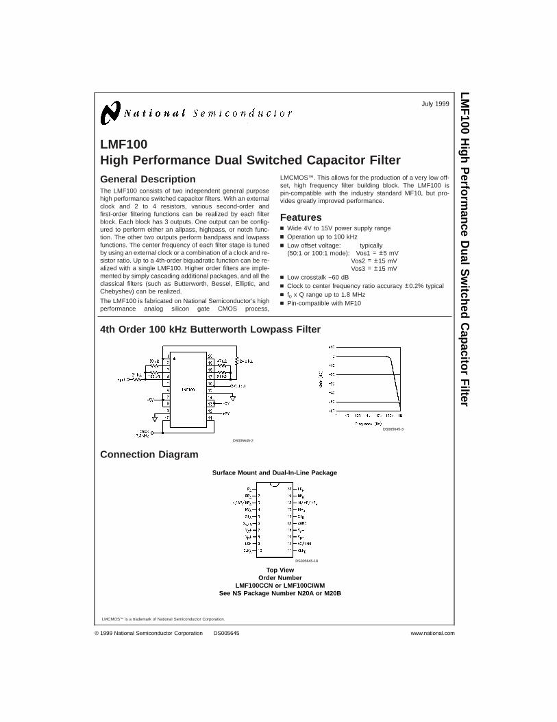
4th Order 100 kHz Butterworth Lowpass Filter
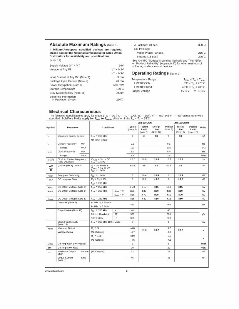
Connection Diagram
LMCMOS™ is a trademark of National Semiconductor Corporation.
DS005645-2
DS005645-3
Surface Mount and Dual-In-Line Package
DS005645-18
Top ViewOrder Number
LMF100CCN or LMF100CIWMSee NS Package Number N20A or M20B
July 1999
LMF100
High
Perform
anceD
ualSw
itchedC
apacitorFilter
© 1999 National Semiconductor Corporation DS005645 www.national.com
Absolute Maximum Ratings (Note 1)
If Military/Aerospace specified devices are required,please contact the National Semiconductor Sales Office/Distributors for availability and specifications.
(Note 14)
Supply Voltage (V+ − V−) 16VVoltage at Any Pin V+ + 0.3V
V− − 0.3VInput Current at Any Pin (Note 2) 5 mAPackage Input Current (Note 2) 20 mAPower Dissipation (Note 3) 500 mWStorage Temperature 150˚CESD Susceptability (Note 11) 2000VSoldering Information
N Package: 10 sec. 260˚C
J Package: 10 sec. 300˚CSO Package:
Vapor Phase (60 sec.) 215˚CInfrared (15 sec.) 220˚C
See AN-450 “Surface Mounting Methods and Their Effecton Product Reliability” (Appendix D) for other methods ofsoldering surface mount devices.
Operating Ratings (Note 1)
Temperature Range TMIN ≤ TA ≤ TMAX
LMF100CCN 0˚C ≤ TA ≤ +70˚CLMF100CIWM −40˚C ≤ TA ≤ +85˚C
Supply Voltage 4V ≤ V+ − V− ≤ 15V
Electrical CharacteristicsThe following specifications apply for Mode 1, Q = 10 (R1 = R3 = 100k, R2 = 10k), V+ = +5V and V− = −5V unless otherwisespecified. Boldface limits apply for T MIN to TMAX; all other limits TA = TJ = 25˚C.
Symbol Parameter Conditions
LMF100CCN LMF100CIWM
UnitsTypical(Note 8)
TestedLimit
(Note 9)
DesignLimit
(Note 10)
Typical(Note 8)
TestedLimit
(Note 9)
DesignLimit
(Note 10)
Is Maximum Supply Current fCLK = 250 kHz 9 13 13 9 13 mA
No Input Signal
f0 Center Frequency MIN 0.1 0.1 Hz
Range MAX 100 100 kHz
fCLK Clock Frequency MIN 5.0 5.0 Hz
Range MAX 3.5 3.5 MHz
fCLK/f0 Clock to Center FrequencyRatio Deviation
VPin12 = 5V or 0VfCLK = 1 MHz
±0.2 ±0.8 ±0.8 ±0.2 ±0.8 %
Q Error (MAX) (Note 4) Q = 10, Mode 1VPin12 = 5V or 0VfCLK = 1 MHz
±0.5 ±5 ±6 ±0.5 ±6 %
HOBP Bandpass Gain at f0 fCLK = 1 MHz 0 ±0.4 ±0.4 0 ±0.4 dB
HOLP DC Lowpass Gain R1 = R2 = 10k 0 ±0.2 ±0.2 0 ±0.2 dB
fCLK = 250 kHz
VOS1 DC Offset Voltage (Note 5) fCLK = 250 kHz ±5.0 ±15 ±15 ±5.0 ±15 mV
VOS2 DC Offset Voltage (Note 5) fCLK = 250 kHz SA/B = V+ ±30 ±80 ±80 ±30 ±80 mV
SA/B = V− ±15 ±70 ±70 ±15 ±70 mV
VOS3 DC Offset Voltage (Note 5) fCLK = 250 kHz ±15 ±40 ±60 ±15 ±60 mV
Crosstalk (Note 6) A Side to B Side or−60 −60 dB
B Side to A Side
Output Noise (Note 12) fCLK = 250 kHz N 40 40
20 kHz Bandwidth BP 320 320 µV
100:1 Mode LP 300 300
Clock Feedthrough(Note 13)
fCLK = 250 kHz 100:1 Mode 6 6 mV
VOUT Minimum Output RL = 5k +4.0±3.8 ±3.7
+4.0±3.7 V
Voltage Swing (All Outputs) −4.7 −4.7
RL = 3.5k +3.9 +3.9V
(All Outputs) −4.6 −4.6
GBW Op Amp Gain BW Product 5 5 MHz
SR Op Amp Slew Rate 20 20 V/µs
Isc Maximum OutputShort
Source (All Outputs) 12 12 mA
Circuit Current(Note 7)
Sink 45 45 mA
www.national.com 2
Electrical Characteristics (Continued)
The following specifications apply for Mode 1, Q = 10 (R1 = R3 = 100k, R2 = 10k), V+ = +5V and V− = −5V unless otherwisespecified. Boldface limits apply for T MIN to TMAX; all other limits TA = TJ = 25˚C.
Symbol Parameter Conditions
LMF100CCN LMF100CIWM
UnitsTypical(Note 8)
TestedLimit
(Note 9)
DesignLimit
(Note 10)
Typical(Note 8)
TestedLimit
(Note 9)
DesignLimit
(Note 10)
IIN Input Current on Pins: 4, 5, 10 10 µA
6, 9, 10, 11, 12, 16, 17
Electrical CharacteristicsThe following specifications apply for Mode 1, Q = 10 (R1 = R3 = 100k, R2 = 10k), V+ = +2.50V and V− = −2.50V unless oth-erwise specified. Boldface limits apply for T MIN to TMAX; all other limits TA = TJ = 25˚C.
Symbol Parameter Conditions
LMF100CCN LMF100CIWM
UnitsTypical(Note 8)
TestedLimit
(Note 9)
DesignLimit(Note10)
Typical(Note 8)
TestedLimit
(Note 9)
DesignLimit(Note10)
Is Maximum SupplyCurrent
fCLK = 250 kHzNo Input Signal 8 12 12 8 12 mA
f0 Center Frequency MIN 0.1 0.1 Hz
Range MAX 50 50 kHz
fCLK Clock Frequency MIN 5.0 5.0 Hz
Range MAX 1.5 1.5 MHz
fCLK/f0 Clock to Center VPin12 = 2.5V or 0V±0.2 ±1 ±1 ±0.2 ±1 %
Frequency Ratio Deviation fCLK = 1 MHz
Q Error (MAX) Q = 10, Mode 1
(Note 4) VPin12 = 5V or 0V ±0.5 ±5 ±8 ±0.5 ±8 %
fCLK = 1 MHz
HOBP Bandpass Gain at f0 fCLK = 1 MHz 0 ±0.4 ±0.5 0 ±0.5 dB
HOLP DC Lowpass Gain R1 = R2 = 10k 0 ±0.2 ±0.2 0 ±0.2 dB
fCLK = 250 kHz
VOS1 DC Offset Voltage (Note 5) fCLK = 250 kHz ±5.0 ±15 ±15 ±5.0 ±15 mV
VOS2 DC Offset Voltage (Note 5) fCLK = 250 kHz SA/B = V+ ±20 ±60 ±60 ±20 ±60 mV
SA/B = V− ±10 ±50 ±60 ±10 ±60 mV
VOS3 DC Offset Voltage (Note 5) fCLK = 250 kHz ±10 ±25 ±30 ±10 ±30 mV
Crosstalk (Note 6) A Side to B Side or −65 −65 dB
B Side to A Side
Output Noise (Note 12) fCLK = 250 kHz N 25 25
20 kHz Bandwidth BP 250 250 µV
100:1 Mode LP 220 220
Clock Feedthrough (Note 13) fCLK = 250 kHz 100:1 Mode 2 2 mV
VOUT Minimum Output RL = 5k +1.6±1.5 ±1.4
+1.6±1.4 V
Voltage Swing (All Outputs) −2.2 −2.2
RL = 3.5k +1.5 +1.5 V
(All outputs) −2.1 −2.1
GBW Op Amp Gain BW Product 5 5 MHz
SR Op Amp Slew Rate 18 18 V/µs
Isc Maximum OutputShort Circuit
Source (All Outputs) 10 10 mA
Current (Note 7) Sink 20 20 mA
www.national.com3

Logic Input CharacteristicsBoldface limits apply for T MIN to TMAX; all other limits TA = TJ = 25˚C.
Parameter Conditions
LMF100CCN LMF100CIWM
UnitsTypical Tested Design Typical Tested Design
(Note 8) Limit Limit (Note 8) Limit Limit
(Note 9) (Note 10) (Note 9) (Note 10)
CMOS Clock MIN Logical “1” V+ = +5V, V− = −5V, +3.0 +3.0 +3.0 V
Input Voltage MAX Logical “0” VLSh = 0V −3.0 −3.0 −3.0 V
MIN Logical “1” V+ = +10V, V− = 0V, +8.0 +8.0 +8.0 V
MAX Logical “0” VLSh = +5V +2.0 +2.0 +2.0 V
TTL Clock MIN Logical “1” V+ = +5V, V− = −5V, +2.0 +2.0 +2.0 V
Input Voltage MAX Logical “0” VLSh = 0V +0.8 +0.8 +0.8 V
MIN Logical “1” V+ = +10V, V− = 0V, +2.0 +2.0 +2.0 V
MAX Logical “0” VLSh = 0V +0.8 +0.8 +0.8 V
CMOS Clock MIN Logical “1” V+ = +2.5V, V− = −2.5V, +1.5 +1.5 +1.5 V
Input Voltage MAX Logical “0” VLSh = 0V −1.5 −1.5 −1.5 V
MIN Logical “1” V+ = +5V, V− = 0V, +4.0 +4.0 +4.0 V
MAX Logical “0” VLSh = +2.5V +1.0 +1.0 +1.0 V
TTL Clock MIN Logical “1” V+ = +5V, V− = 0V, +2.0 +2.0 +2.0 V
Input Voltage MAX Logical “0” VLSh = 0V, VD+ = 0V +0.8 +0.8 +0.8 V
Note 1: Absolute Maximum Ratings indicate limits beyond which damage to the device may occur. Operating Ratings indicate conditions for which the device is in-tended to be functional. These ratings do not guarantee specific performance limits, however. For guaranteed specifications and test conditions, see the ElectricalCharacteristics. The guaranteed specifications apply only for the test conditions listed. Some performance characteristics may degrade when the device is not op-erated under the listed test conditions.
Note 2: When the input voltage (VIN) at any pin exceeds the power supply rails (VIN < V− or VIN > V+) the absolute value of current at that pin should be limitedto 5 mA or less. The sum of the currents at all pins that are driven beyond the power supply voltages should not exceed 20 mA.
Note 3: The maximum power dissipation must be derated at elevated temperatures and is dictated by TJMAX, θJA, and the ambient temperature, TA. The maximumallowable power dissipation at any temperature is PD = (TJMAX − TA)/θJA or the number given in the Absolute Maximum Ratings, whichever is lower. For this device,TJMAX = 125˚C, and the typical junction-to-ambient thermal resistance of the LMF100CIN when board mounted is 55˚C/W. For the LMF100CIWM this number is66˚C/W.
Note 4: The accuracy of the Q value is a function of the center frequency (f0). This is illustrated in the curves under the heading “Typical Peformance Characteristics”.
Note 5: Vos1, Vos2, and Vos3 refer to the internal offsets as discussed in the Applications Information section 3.4.
Note 6: Crosstalk between the internal filter sections is measured by applying a 1 VRMS 10 kHz signal to one bandpass filter section input and grounding the inputof the other bandpass filter section. The crosstalk is the ratio between the output of the grounded filter section and the 1 VRMS input signal of the other section.
Note 7: The short circuit source current is measured by forcing the output that is being tested to its maximum positive voltage swing and then shorting that outputto the negative supply. The short circuit sink current is measured by forcing the output that is being tested to its maximum negative voltage swing and then shortingthat output to the positive supply. These are the worst case conditions.
Note 8: Typicals are at 25˚C and represent most likely parametric norm.
Note 9: Tested limits are guaranteed to National’s AOQL (Average Outgoing Quality Level).
Note 10: Design limits are guaranteed to National’s AOQL (Average Outgoing Quality Level) but are not 100% tested.
Note 11: Human body model, 100 pF discharged through a 1.5 kΩ resistor.
Note 12: In 50:1 mode the output noise is 3 dB higher.
Note 13: In 50:1 mode the clock feedthrough is 6 dB higher.
Note 14: A military RETS specification is available upon request.
www.national.com 4
Typical Performance Characteristics
Power Supply Current vsPower Supply Voltage
DS005645-40
Power Supply Current vsTemperature
DS005645-41
Output Swing vsSupply Voltage
DS005645-42
Positive Output Swingvs Temperature
DS005645-43
Negative Output Swingvs Temperature
DS005645-44
Positive Output VoltageSwing vs Load Resistance
DS005645-45
Negative Output VoltageSwing vs Load Resistance
DS005645-46
fCLK/f0 Ratio vs Q
DS005645-47
fCLK/f0 Ratio vs Q
DS005645-48
fCLK/f0 Ratio vs f CLK
DS005645-49
fCLK/f0 Ratio vs f CLK
DS005645-50
fCLK/f0 Ratio vs f CLK
DS005645-51
www.national.com5

Typical Performance Characteristics (Continued)
fCLK/f0 Ratio vs f CLK
DS005645-52
fCLK/f0 Ratio vs Temperature
DS005645-53
fCLK/f0 Ratio vs Temperature
DS005645-54
Q Deviation vs ClockFrequency
DS005645-55
Q Deviation vs ClockFrequency
DS005645-56
Q Deviation vs ClockFrequency
DS005645-57
Q Deviation vs ClockFrequency
DS005645-58
Q Deviation vs Temperature
DS005645-59
Q Deviation vs Temperature
DS005645-60
www.national.com 6
Typical Performance Characteristics (Continued)
LMF100 System Block Diagram
Maximum f 0 vs Q atVs = ±7.5V
DS005645-61
Maximum f 0 vs Q atVs = ±5.0V
DS005645-62
Maximum f 0 vs Q atVs = ±2.5V
DS005645-63
DS005645-1
www.national.com7
Pin DescriptionsLP(1,20),BP(2,19),N/AP/HP(3,18)
The second order lowpass,bandpass andnotch/allpass/highpass outputs.These outputs can typically swingto within 1V of each supply whendriving a 5 kΩ load. For optimumperformance, capacitive loadingon these outputs should beminimized. For signal frequenciesabove 15 kHz the capacitanceloading should be kept below30 pF.
INV(4,17) The inverting input of thesumming opamp of each filter.These are high impedance inputs.The non-inverting input isinternally tied to AGND so theopamp can be used only as aninverting amplifier.
S1(5,16) S1 is a signal input pin used inmodes 1b, 4, and 5. The inputimpedance is 1/fCLK x 1 pF. Thepin should be driven with a sourceimpedance of less than 1 kΩ. IfS1 is not driven with a signal itshould be tied to AGND(mid-supply).
SA/B(6) This pin activates a switch thatconnects one of the inputs of eachfilter’s second summer either toAGND (SA/B tied to V−) or to thelowpass (LP) output (SA/B tied toV+). This offers the flexibilityneeded for configuring the filter inits various modes of operation.
VA+(7) (Note 15) This is both the analog and digital
positive supply.
VD+(8) (Note 15) This pin needs to be tied to V+
except when the device is tooperate on a single 5V supply anda TTL level clock is applied. For5V, TTL operation, VD
+ should betied to ground (0V).
VA−(14), VD
−(13) Analog and digital negativesupplies. VA
−and VD− should be
derived from the same source.They have been brought outseparately so they can bebypassed by separate capacitors,if desired. They can also be tiedtogether externally and bypassedwith a single capacitor.
LSh(9) Level shift pin. This is used toaccommodate various clock levelswith dual or single supplyoperation. With dual ±5V suppliesand CMOS (±5V) or TTL (0V–5V)clock levels, LSh should be tied tosystem ground.
For 0V–10V single supplyoperation the AGND pin should bebiased at +5V and the LSh pinshould be tied to the systemground for TTL clock levels. LShshould be biased at +5V for ±5VCMOS clock levels.
The LSh pin is tied to systemground for ±2.5V operation. Forsingle 5V operation the LSh andVD+ pins are tied to systemground for TTL clock levels.
CLK(10,11) Clock inputs for the two switchedcapacitor filter sections. Unipolaror bipolar clock levels may beapplied to the CLK inputsaccording to the programmingvoltage applied to the LSh pin.The duty cycle of the clock shouldbe close to 50%, especially whenclock frequencies above 200 kHzare used. This allows themaximum time for the internalopamps to settle, which yieldsoptimum filter performance.
50/100(12)(Note 15)
By tying this pin to V+ a 50:1 clockto filter center frequency ratio isobtained. Tying this pin atmid-supply (i.e., system groundwith dual supplies) or to V− allowsthe filter to operate at a 100:1clock to center frequency ratio.
AGND(15) This is the analog ground pin.This pin should be connected tothe system ground for dual supplyoperation or biased to mid-supplyfor single supply operation. For afurther discussion of mid-supplybiasing techniques see theApplications Information (Section3.2). For optimum filterperformance a “clean” groundmust be provided.
Note 15: This device is pin-for-pin compatible with the MF10 except for thefollowing changes:
1. Unlike the MF10, the LMF100 has a single positive supply pin (VA+).
2. On the LMF100 VD+ is a control pin and is not the digital positive supply as
on the MF10.
3. Unlike the MF10, the LMF100 does not support the current limiting mode.When the 50/100 pin is tied to V− the LMF100 will remain in the 100:1 mode.
www.national.com 8

1.0 Definitions of TermsfCLK: the frequency of the external clock signal applied to pin10 or 11.
f0: center frequency of the second order function complexpole pair. f0 is measured at the bandpass outputs of theLMF100, and is the frequency of maximum bandpass gain.(Figure 1).
fnotch : the frequency of minimum (ideally zero) gain at thenotch outputs.
fz: the center frequency of the second order complex zeropair, if any. If fz is different from f0 and if Qz is high, it can beobserved as the frequency of a notch at the allpass output.(Figure 13).
Q: “quality factor” of the 2nd order filter. Q is measured at thebandpass outputs of the LMF100 and is equal to f0 dividedby the −3 dB bandwidth of the 2nd order bandpass filter (Fig-ure 1). The value of Q determines the shape of the 2nd orderfilter responses as shown in Figure 6.
Qz: the quality factor of the second order complex zero pair,if any. QZ is related to the allpass characteristic, which iswritten:
where QZ = Q for an all-pass response.
HOBP: the gain (in V/V) of the bandpass output at f = f0.
HOLP: the gain (in V/V) of the lowpass output as f → 0 Hz(Figure 2).
HOHP: the gain (in V/V) of the highpass output as f → fCLK/2(Figure 3).
HON: the gain (in V/V) of the notch output as f → 0 Hz and asf → fCLK/2, when the notch filter has equal gain above andbelow the center frequency (Figure 4). When thelow-frequency gain differs from the high-frequency gain, asin modes 2 and 3a (Figure 10 and Figure 12), the two quan-tities below are used in place of HON.
HON1: the gain (in V/V) of the notch output as f → 0 Hz.
HON2: the gain (in V/V) of the notch output as f → fCLK/2.
DS005645-19
(a)DS005645-20
(b)
FIGURE 1. 2nd-Order Bandpass Response
www.national.com9

1.0 Definitions of Terms (Continued)
DS005645-21
(a)DS005645-22
(b)
FIGURE 2. 2nd-Order Low-Pass Response
DS005645-23
(a)DS005645-24
(b)
FIGURE 3. 2nd-Order High-Pass Response
www.national.com 10

1.0 Definitions of Terms (Continued)
DS005645-25
(a)DS005645-26
(b)
FIGURE 4. 2nd-Order Notch Response
DS005645-27
(a)DS005645-28
(b)
FIGURE 5. 2nd-Order All-Pass Response
www.national.com11
1.0 Definitions of Terms (Continued)
(a) Bandpass
DS005645-64
(b) Low Pass
DS005645-65
(c) High-Pass
DS005645-66
(d) Notch
DS005645-67
(e) All-Pass
DS005645-68
FIGURE 6. Response of various 2nd-order filters as a function of Q. Gainsand center frequencies are normalized to unity.
www.national.com 12
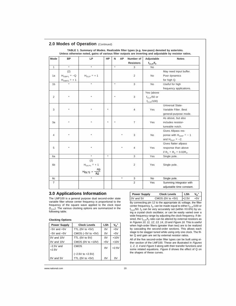
2.0 Modes of OperationThe LMF100 is a switched capacitor (sampled data) filter. Tofully describe its transfer functions, a time domain analysis isappropriate. Since this is cumbersome, and since theLMF100 closely approximates continuous filters, the follow-ing discussion is based on the well-known frequency do-main. Each LMF100 can produce two full 2nd order func-tions. See Table 1 for a summary of the characteristics of thevarious modes.
MODE 1: Notch 1, Bandpass, Lowpass Outputs:
fnotch = f0 (See Figure 7)
MODE 1a: Non-Inverting BP, LP (See Figure 8)
Note: VIN should be driven from a low impedance (<1 kΩ) source.
DS005645-11
FIGURE 7. MODE 1
DS005645-4
FIGURE 8. MODE 1a
www.national.com13
2.0 Modes of Operation (Continued)
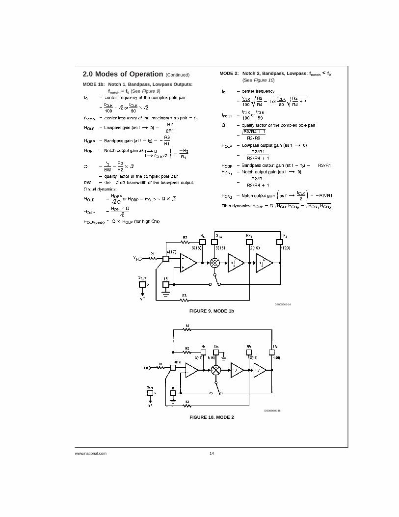
MODE 1b: Notch 1, Bandpass, Lowpass Outputs:
fnotch = f0 (See Figure 9)
MODE 2: Notch 2, Bandpass, Lowpass: f notch < f0(See Figure 10)
DS005645-14
FIGURE 9. MODE 1b
DS005645-36
FIGURE 10. MODE 2
www.national.com 14

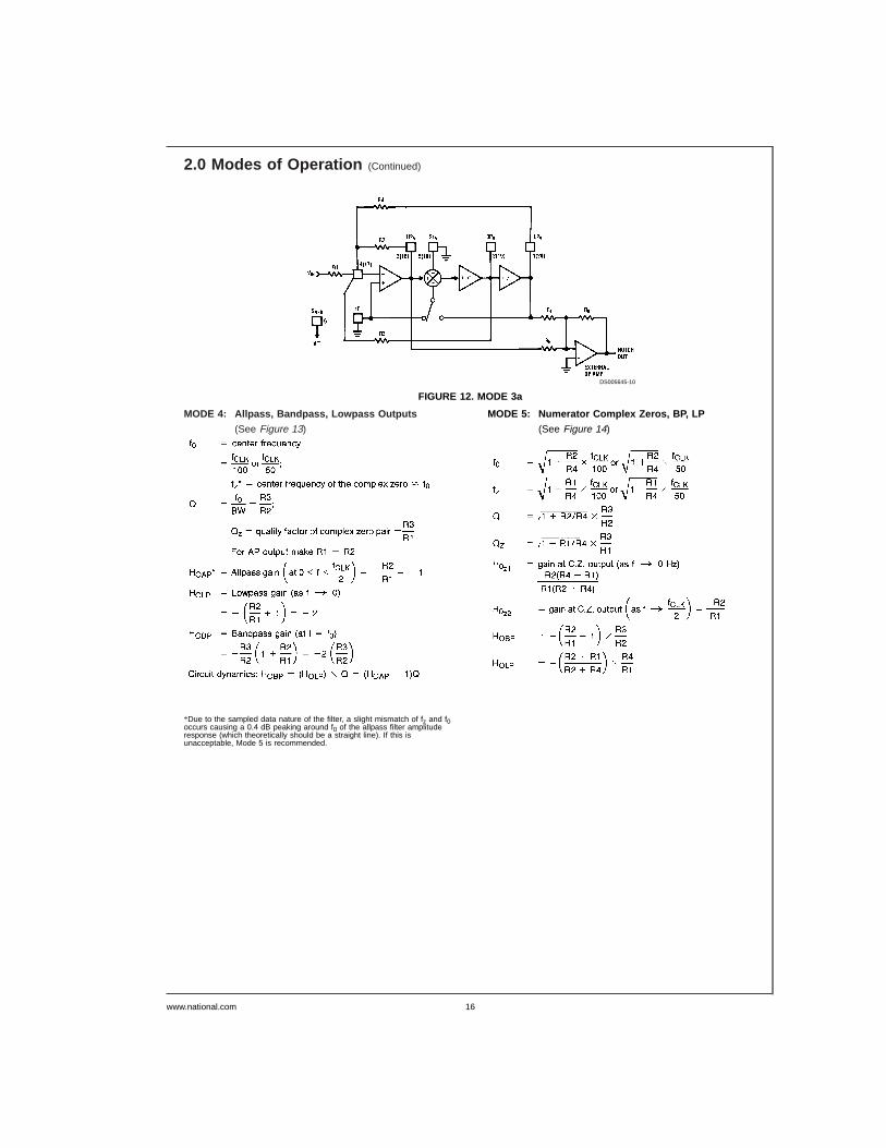
2.0 Modes of Operation (Continued)
MODE 3: Highpass, Bandpass, Lowpass Outputs
(See Figure 11)
MODE 3a: HP, BP, LP and Notch with External Op Amp
(See Figure 12)
DS005645-5
*In Mode 3, the feedback loop is closed around the input summing amplifier; the finite GBW product of this op amp causes a slight Q enhancement. If this is aproblem, connect a small capacitor (10 pF−100 pF) across R4 to provide some phase lead.
FIGURE 11. MODE 3
www.national.com15
2.0 Modes of Operation (Continued)
MODE 4: Allpass, Bandpass, Lowpass Outputs
(See Figure 13)
*Due to the sampled data nature of the filter, a slight mismatch of fz and f0occurs causing a 0.4 dB peaking around f0 of the allpass filter amplituderesponse (which theoretically should be a straight line). If this isunacceptable, Mode 5 is recommended.
MODE 5: Numerator Complex Zeros, BP, LP
(See Figure 14)
DS005645-10
FIGURE 12. MODE 3a
www.national.com 16

2.0 Modes of Operation (Continued)
MODE 6a: Single Pole, HP, LP Filter (See Figure 15)
DS005645-6
FIGURE 13. MODE 4
DS005645-15
FIGURE 14. MODE 5
DS005645-16
FIGURE 15. MODE 6a
www.national.com17
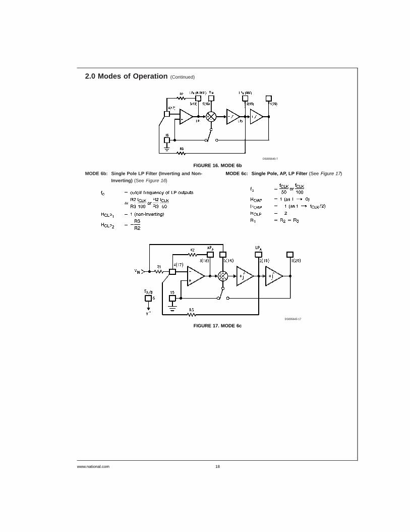
2.0 Modes of Operation (Continued)
MODE 6b: Single Pole LP Filter (Inverting and Non-
Inverting) (See Figure 16)
MODE 6c: Single Pole, AP, LP Filter (See Figure 17)
DS005645-7
FIGURE 16. MODE 6b
DS005645-17
FIGURE 17. MODE 6c
www.national.com 18
2.0 Modes of Operation (Continued)
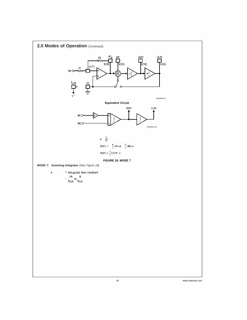
MODE 7: Summing Integrator (See Figure 18)
DS005645-37
Equivalent Circuit
DS005645-38
FIGURE 18. MODE 7
www.national.com19
2.0 Modes of Operation (Continued)
TABLE 1. Summary of Modes. Realizable filter types (e.g. low-pass) denoted by asterisks.Unless otherwise noted, gains of various filter outputs are inverting and adjustable by resistor ratios.
Mode BP LP HP N AP Number of Adjustable Notes
Resistors f CLK/f01 * * * 3 No
(2) May need input buffer.
1a HOBP1 = −Q HOLP = + 1 2 No Poor dynamics
HOBP2 = + 1 for high Q.
1b * * * 3 No Useful for high
frequency applications.
Yes (above
2 * * * 3 fCLK/50 or
fCLK/100)
Universal State-
3 * * * 4 Yes Variable Filter. Best
general-purpose mode.
As above, but also
3a * * * * 7 Yes includes resistor-
tuneable notch.
Gives Allpass res-
4 * * * 3 No ponse with HOAP = − 1
and HOLP = −2.
Gives flatter allpass
5 * * * 4 Yes response than above
if R1 = R2 = 0.02R4.
6a * * 3 Yes Single pole.
(2)
6b HOLP1 = + 1 2 Yes Single pole.
6c * * 3 No Single pole.
7 2 Yes Summing integrator with
adjustable time constant.
3.0 Applications InformationThe LMF100 is a general purpose dual second-order statevariable filter whose center frequency is proportional to thefrequency of the square wave applied to the clock input(fCLK). The various clocking options are summarized in thefollowing table.
Clocking Options
Power Supply Clock Levels LSh V D+
−5V and +5V TTL (0V to +5V) 0V +5V
−5V and +5V CMOS (−5V to +5V) 0V +5V
0V and 10V TTL (0V to 5V) 0V +10V
0V and 10V CMOS (0V to +10V) +5V +10V
−2.5V and+2.5V
CMOS0V +2.5V
(−2.5V to +2.5V)
0V and 5V TTL (0V to +5V) 0V 0V
Power Supply Clock Levels LSh V D+
0V and 5V CMOS (0V to +5V) +2.5V +5V
By connecting pin 12 to the appropriate dc voltage, the filtercenter frequency, f0, can be made equal to either fCLK/100 orfCLK/50. f0 can be very accurately set (within ±0.6%) by us-ing a crystal clock oscillator, or can be easily varied over awide frequency range by adjusting the clock frequency. If de-sired, the fCLK/f0 ratio can be altered by external resistors asin Figures 10, 11, 12, 13, 14, 15 and Figure 16. This is usefulwhen high-order filters (greater than two) are to be realizedby cascading the second-order sections. This allows eachstage to be stagger tuned while using only one clock. The fil-ter Q and gain are set by external resistor ratios.
All of the five second-order filter types can be built using ei-ther section of the LMF100. These are illustrated in Figures1, 2, 3, 4 and Figure 5 along with their transfer functions andsome related equations. Figure 6 shows the effect of Q onthe shapes of these curves.
www.national.com 20
3.0 Applications Information(Continued)
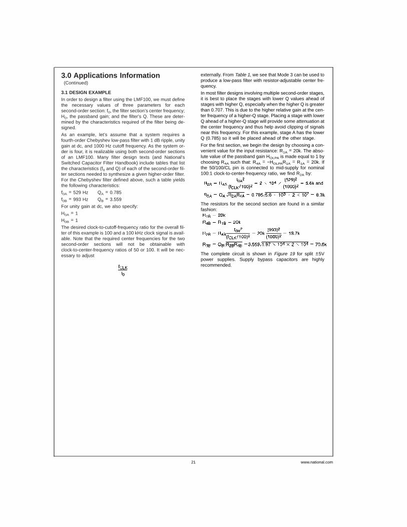
3.1 DESIGN EXAMPLE
In order to design a filter using the LMF100, we must definethe necessary values of three parameters for eachsecond-order section: f0, the filter section’s center frequency;H0, the passband gain; and the filter’s Q. These are deter-mined by the characteristics required of the filter being de-signed.
As an example, let’s assume that a system requires afourth-order Chebyshev low-pass filter with 1 dB ripple, unitygain at dc, and 1000 Hz cutoff frequency. As the system or-der is four, it is realizable using both second-order sectionsof an LMF100. Many filter design texts (and National’sSwitched Capacitor Filter Handbook) include tables that listthe characteristics (f0 and Q) of each of the second-order fil-ter sections needed to synthesize a given higher-order filter.For the Chebyshev filter defined above, such a table yieldsthe following characteristics:
f0A = 529 Hz QA = 0.785
f0B = 993 Hz QB = 3.559
For unity gain at dc, we also specify:
H0A = 1
H0B = 1
The desired clock-to-cutoff-frequency ratio for the overall fil-ter of this example is 100 and a 100 kHz clock signal is avail-able. Note that the required center frequencies for the twosecond-order sections will not be obtainable withclock-to-center-frequency ratios of 50 or 100. It will be nec-essary to adjust
externally. From Table 1, we see that Mode 3 can be used toproduce a low-pass filter with resistor-adjustable center fre-quency.
In most filter designs involving multiple second-order stages,it is best to place the stages with lower Q values ahead ofstages with higher Q, especially when the higher Q is greaterthan 0.707. This is due to the higher relative gain at the cen-ter frequency of a higher-Q stage. Placing a stage with lowerQ ahead of a higher-Q stage will provide some attenuation atthe center frequency and thus help avoid clipping of signalsnear this frequency. For this example, stage A has the lowerQ (0.785) so it will be placed ahead of the other stage.
For the first section, we begin the design by choosing a con-venient value for the input resistance: R1A = 20k. The abso-lute value of the passband gain HOLPA is made equal to 1 bychoosing R4A such that: R4A = −HOLPAR1A = R1A = 20k. Ifthe 50/100/CL pin is connected to mid-supply for nominal100:1 clock-to-center-frequency ratio, we find R2A by:
The resistors for the second section are found in a similarfashion:
The complete circuit is shown in Figure 19 for split ±5Vpower supplies. Supply bypass capacitors are highlyrecommended.
www.national.com21
3.0 Applications Information (Continued)
DS005645-30
FIGURE 19. Fourth-order Chebyshev low-pass filter from example in 3.1.±5V power supply. 0V–5V TTL or ±5V CMOS logic levels.
DS005645-31
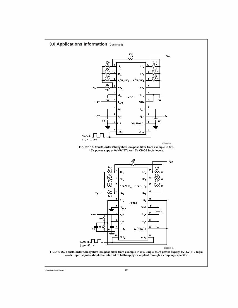
FIGURE 20. Fourth-order Chebyshev low-pass filter from example in 3.1. Single +10V power supply. 0V–5V TTL logiclevels. Input signals should be referred to half-supply or applied through a coupling capacitor.
www.national.com 22
3.0 Applications Information (Continued)
3.2 SINGLE SUPPLY OPERATION
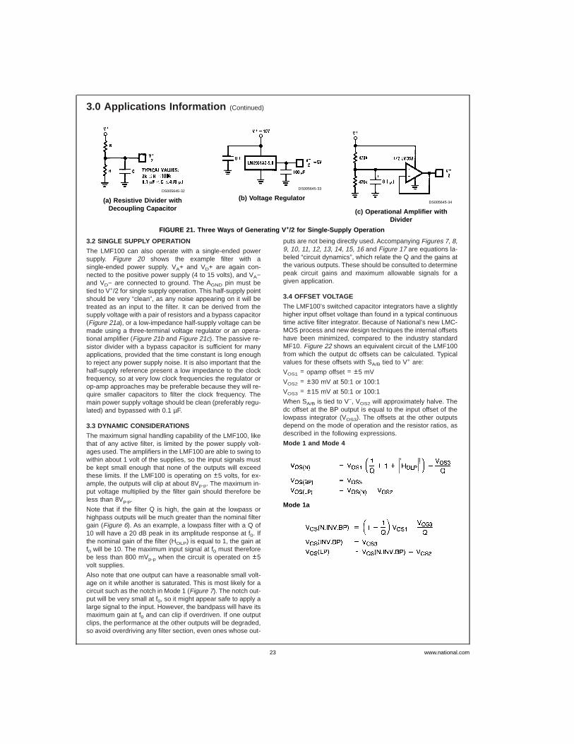
The LMF100 can also operate with a single-ended powersupply. Figure 20 shows the example filter with asingle-ended power supply. VA+ and VD+ are again con-nected to the positive power supply (4 to 15 volts), and VA−and VD− are connected to ground. The AGND pin must betied to V+/2 for single supply operation. This half-supply pointshould be very “clean”, as any noise appearing on it will betreated as an input to the filter. It can be derived from thesupply voltage with a pair of resistors and a bypass capacitor(Figure 21a), or a low-impedance half-supply voltage can bemade using a three-terminal voltage regulator or an opera-tional amplifier (Figure 21b and Figure 21c). The passive re-sistor divider with a bypass capacitor is sufficient for manyapplications, provided that the time constant is long enoughto reject any power supply noise. It is also important that thehalf-supply reference present a low impedance to the clockfrequency, so at very low clock frequencies the regulator orop-amp approaches may be preferable because they will re-quire smaller capacitors to filter the clock frequency. Themain power supply voltage should be clean (preferably regu-lated) and bypassed with 0.1 µF.
3.3 DYNAMIC CONSIDERATIONS
The maximum signal handling capability of the LMF100, likethat of any active filter, is limited by the power supply volt-ages used. The amplifiers in the LMF100 are able to swing towithin about 1 volt of the supplies, so the input signals mustbe kept small enough that none of the outputs will exceedthese limits. If the LMF100 is operating on ±5 volts, for ex-ample, the outputs will clip at about 8Vp-p. The maximum in-put voltage multiplied by the filter gain should therefore beless than 8Vp-p.
Note that if the filter Q is high, the gain at the lowpass orhighpass outputs will be much greater than the nominal filtergain (Figure 6). As an example, a lowpass filter with a Q of10 will have a 20 dB peak in its amplitude response at f0. Ifthe nominal gain of the filter (HOLP) is equal to 1, the gain atf0 will be 10. The maximum input signal at f0 must thereforebe less than 800 mVp-p when the circuit is operated on ±5volt supplies.
Also note that one output can have a reasonable small volt-age on it while another is saturated. This is most likely for acircuit such as the notch in Mode 1 (Figure 7). The notch out-put will be very small at f0, so it might appear safe to apply alarge signal to the input. However, the bandpass will have itsmaximum gain at f0 and can clip if overdriven. If one outputclips, the performance at the other outputs will be degraded,so avoid overdriving any filter section, even ones whose out-
puts are not being directly used. Accompanying Figures 7, 8,9, 10, 11, 12, 13, 14, 15, 16 and Figure 17 are equations la-beled “circuit dynamics”, which relate the Q and the gains atthe various outputs. These should be consulted to determinepeak circuit gains and maximum allowable signals for agiven application.
3.4 OFFSET VOLTAGE
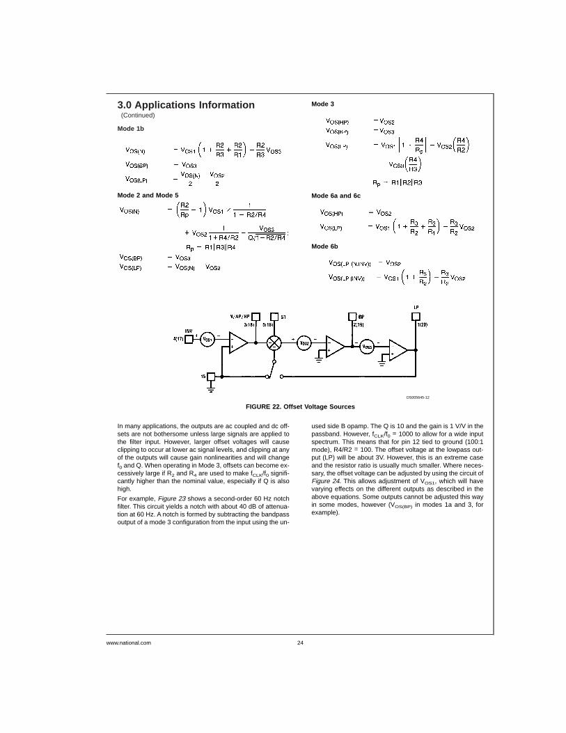
The LMF100’s switched capacitor integrators have a slightlyhigher input offset voltage than found in a typical continuoustime active filter integrator. Because of National’s new LMC-MOS process and new design techniques the internal offsetshave been minimized, compared to the industry standardMF10. Figure 22 shows an equivalent circuit of the LMF100from which the output dc offsets can be calculated. Typicalvalues for these offsets with SA/B tied to V+ are:
VOS1 = opamp offset = ±5 mV
VOS2 = ±30 mV at 50:1 or 100:1
VOS3 = ±15 mV at 50:1 or 100:1
When SA/B is tied to V−, VOS2 will approximately halve. Thedc offset at the BP output is equal to the input offset of thelowpass integrator (VOS3). The offsets at the other outputsdepend on the mode of operation and the resistor ratios, asdescribed in the following expressions.
Mode 1 and Mode 4
Mode 1a
DS005645-32
(a) Resistive Divider withDecoupling Capacitor
DS005645-33
(b) Voltage RegulatorDS005645-34
(c) Operational Amplifier withDivider
FIGURE 21. Three Ways of Generating V +/2 for Single-Supply Operation
www.national.com23
3.0 Applications Information(Continued)
Mode 1b
Mode 2 and Mode 5
Mode 3
Mode 6a and 6c
Mode 6b
In many applications, the outputs are ac coupled and dc off-sets are not bothersome unless large signals are applied tothe filter input. However, larger offset voltages will causeclipping to occur at lower ac signal levels, and clipping at anyof the outputs will cause gain nonlinearities and will changef0 and Q. When operating in Mode 3, offsets can become ex-cessively large if R2 and R4 are used to make fCLK/f0 signifi-cantly higher than the nominal value, especially if Q is alsohigh.
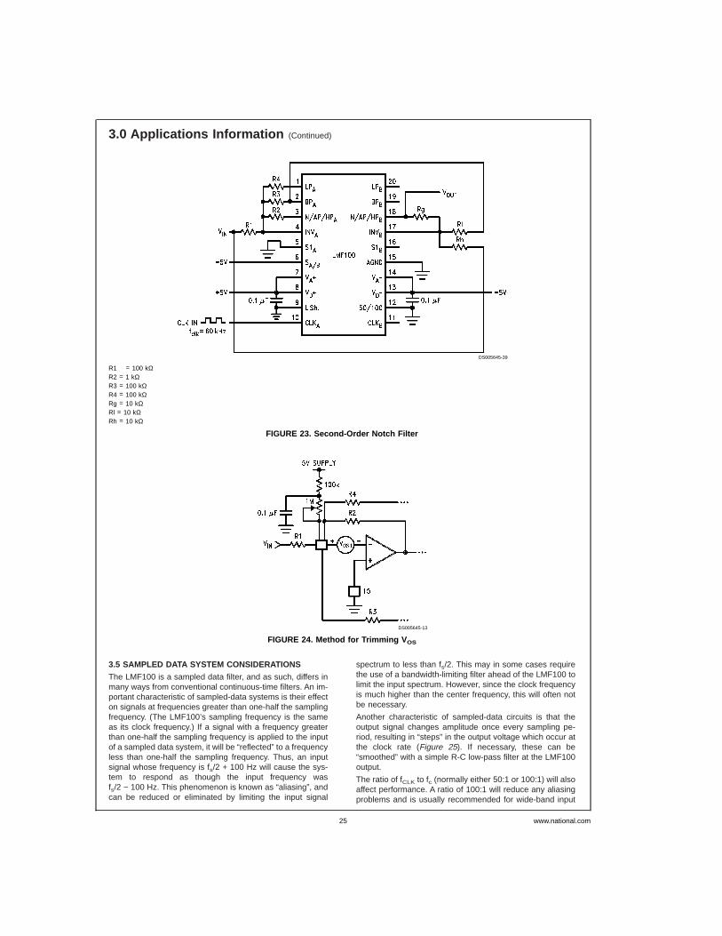
For example, Figure 23 shows a second-order 60 Hz notchfilter. This circuit yields a notch with about 40 dB of attenua-tion at 60 Hz. A notch is formed by subtracting the bandpassoutput of a mode 3 configuration from the input using the un-
used side B opamp. The Q is 10 and the gain is 1 V/V in thepassband. However, fCLK/f0 = 1000 to allow for a wide inputspectrum. This means that for pin 12 tied to ground (100:1mode), R4/R2 = 100. The offset voltage at the lowpass out-put (LP) will be about 3V. However, this is an extreme caseand the resistor ratio is usually much smaller. Where neces-sary, the offset voltage can be adjusted by using the circuit ofFigure 24. This allows adjustment of VOS1, which will havevarying effects on the different outputs as described in theabove equations. Some outputs cannot be adjusted this wayin some modes, however (VOS(BP) in modes 1a and 3, forexample).
DS005645-12
FIGURE 22. Offset Voltage Sources
www.national.com 24
3.0 Applications Information (Continued)
3.5 SAMPLED DATA SYSTEM CONSIDERATIONS
The LMF100 is a sampled data filter, and as such, differs inmany ways from conventional continuous-time filters. An im-portant characteristic of sampled-data systems is their effecton signals at frequencies greater than one-half the samplingfrequency. (The LMF100’s sampling frequency is the sameas its clock frequency.) If a signal with a frequency greaterthan one-half the sampling frequency is applied to the inputof a sampled data system, it will be “reflected” to a frequencyless than one-half the sampling frequency. Thus, an inputsignal whose frequency is fs/2 + 100 Hz will cause the sys-tem to respond as though the input frequency wasfs/2 − 100 Hz. This phenomenon is known as “aliasing”, andcan be reduced or eliminated by limiting the input signal
spectrum to less than fs/2. This may in some cases requirethe use of a bandwidth-limiting filter ahead of the LMF100 tolimit the input spectrum. However, since the clock frequencyis much higher than the center frequency, this will often notbe necessary.
Another characteristic of sampled-data circuits is that theoutput signal changes amplitude once every sampling pe-riod, resulting in “steps” in the output voltage which occur atthe clock rate (Figure 25). If necessary, these can be“smoothed” with a simple R-C low-pass filter at the LMF100output.
The ratio of fCLK to fc (normally either 50:1 or 100:1) will alsoaffect performance. A ratio of 100:1 will reduce any aliasingproblems and is usually recommended for wide-band input
DS005645-39
R1 = 100 kΩR2 = 1 kΩR3 = 100 kΩR4 = 100 kΩRg = 10 kΩRl = 10 kΩRh = 10 kΩ
FIGURE 23. Second-Order Notch Filter
DS005645-13
FIGURE 24. Method for Trimming V OS
www.national.com25

3.0 Applications Information(Continued)
signals. In noise-sensitive applications, a ratio of 100:1 willresult in 3 dB lower output noise for the same filter configu-ration.
The accuracy of the fCLK/f0 ratio is dependent on the value ofQ. This is illustrated in the curves under the heading “Typical
Performance Characteristics”. As Q is changed, the truevalue of the ratio changes as well. Unless the Q is low, theerror in fCLK/f0 will be small. If the error is too large for a spe-cific application, use a mode that allows adjustment of the ra-tio with external resistors.
DS005645-35
FIGURE 25. The Sampled-Data Output Waveform
www.national.com 26
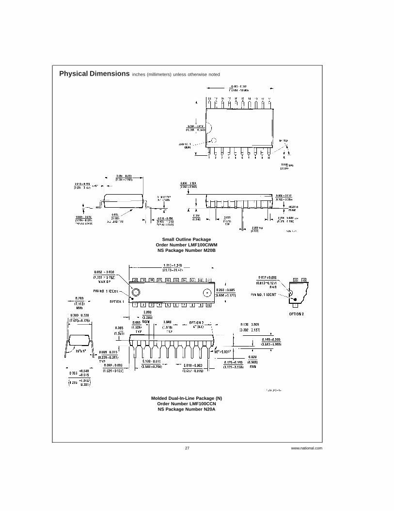
Physical Dimensions inches (millimeters) unless otherwise noted
Small Outline PackageOrder Number LMF100CIWMNS Package Number M20B
Molded Dual-In-Line Package (N)Order Number LMF100CCNNS Package Number N20A
www.national.com27
Notes
LIFE SUPPORT POLICY
NATIONAL’S PRODUCTS ARE NOT AUTHORIZED FOR USE AS CRITICAL COMPONENTS IN LIFE SUPPORTDEVICES OR SYSTEMS WITHOUT THE EXPRESS WRITTEN APPROVAL OF THE PRESIDENT AND GENERALCOUNSEL OF NATIONAL SEMICONDUCTOR CORPORATION. As used herein:
1. Life support devices or systems are devices orsystems which, (a) are intended for surgical implantinto the body, or (b) support or sustain life, andwhose failure to perform when properly used inaccordance with instructions for use provided in thelabeling, can be reasonably expected to result in asignificant injury to the user.
2. A critical component is any component of a lifesupport device or system whose failure to performcan be reasonably expected to cause the failure ofthe life support device or system, or to affect itssafety or effectiveness.
National SemiconductorCorporationAmericasTel: 1-800-272-9959Fax: 1-800-737-7018Email: [email protected]
National SemiconductorEurope
Fax: +49 (0) 1 80-530 85 86Email: [email protected]
Deutsch Tel: +49 (0) 1 80-530 85 85English Tel: +49 (0) 1 80-532 78 32Français Tel: +49 (0) 1 80-532 93 58Italiano Tel: +49 (0) 1 80-534 16 80
National SemiconductorAsia Pacific CustomerResponse GroupTel: 65-2544466Fax: 65-2504466Email: [email protected]
National SemiconductorJapan Ltd.Tel: 81-3-5639-7560Fax: 81-3-5639-7507
www.national.com
LMF1
00H
igh
Per
form
ance
Dua
lSw
itche
dC
apac
itor
Filte
r
National does not assume any responsibility for use of any circuitry described, no circuit patent licenses are implied and National reserves the right at any time without notice to change said circuitry and specifications.