switched-capacitor-cell-based voltage multipliers … et al.: switched-capacitor-cell-based voltage...
TRANSCRIPT
1598 IEEE TRANSACTIONS ON INDUSTRY APPLICATIONS, VOL. 48, NO. 5, SEPTEMBER/OCTOBER 2012
Switched-Capacitor-Cell-Based VoltageMultipliers and DC–AC Inverters
Ke Zou, Student Member, IEEE, Mark J. Scott, Student Member, IEEE, and Jin Wang, Member, IEEE
Abstract—In this paper, several modular converter topologiesbased on a switched-capacitor-cell concept are introduced forhigh-power applications. Two types of switched-capacitor cells,including the full cell and the half-cell, are discussed. The fullcell can be used for dc–ac inversion, and the half-cell is utilizedin both dc–dc and dc–ac applications. A rotational chargingscheme is adopted for the half-cell-based dc–dc voltage multiplierto eliminate the large output capacitor that exists in many tra-ditional switched-capacitor topologies. A soft-switching scheme,which does not require extra components, is adopted to reducethe switching loss and electromagnetic interference. A variableswitching frequency control scheme is proposed to realize softswitching for dc–ac inverters. The experimental results on a 2-kWprototype are presented to verify the proposed topologies.
Index Terms—Soft switching, switched-capacitor converters,variable frequency control.
I. INTRODUCTION
SWITCHED-CAPACITOR converters contain only capac-itors and switching devices. The absence of magnetic
components helps to shrink the system volume and cost. Forthis reason, they have been extensively used in low-powerapplications. Various topologies and control methods havebeen proposed and applied [1]–[5]. However, many classicalswitched-capacitor topologies, such as the traditional charge-pump circuit, require either large voltage stress on componentsor huge input/output capacitors. Moreover, the traditionallyuncontrolled capacitor charging current generates large currentstress on semiconductor switches, reduces the efficiency of theconverter, and introduces a large amount of EMI noise, whichmakes most classical switched-capacitor topologies and controlmethods unsuitable for higher power applications.
Several topologies have been developed in recent years tosolve the aforementioned problems. For dc–dc conversion, aswitched-capacitor dc–dc converter based on the generalizedmultilevel converter topology was presented in [6]. The 1-kWprototype introduced in this paper can realize bidirectionalpower conversion between a 42-V battery and 14-V or 42-V
Manuscript received June 18, 2011; revised November 9, 2011; acceptedFebruary 9, 2012. Date of publication July 19, 2012; date of current versionSeptember 14, 2012. Paper 2011-IPCC-357.R1, presented at the 2011 IEEEApplied Power Electronics Conference and Exposition, Fort Worth, TX, March6–11, and approved for publication in the IEEE TRANSACTIONS ON INDUSTRY
APPLICATIONS by the Industrial Power Converter Committee of the IEEE In-dustry Applications Society. This work was supported by the National ScienceFoundation under Project 1054479.
The authors are with the Department of Electrical and Computer En-gineering, The Ohio State University, Columbus, OH 43210 USA (e-mail:[email protected]; [email protected]; [email protected]).
Color versions of one or more of the figures in this paper are available onlineat http://ieeexplore.ieee.org.
Digital Object Identifier 10.1109/TIA.2012.2209620
loads. In [7], a 3X (i.e., the output voltage is three times ofthe input voltage) dc–dc multiplier/divider was proposed, anda 55-kW prototype for hybrid electric vehicles was built. In[8], a multilevel modular capacitor-clamped dc–dc converter(MMCCC) topology was proposed with many benefits, includ-ing its modular structure, low current, and voltage stress of theswitches and its bidirectional operation capability. However, theaforementioned topologies all require a large number of capac-itors, which can significantly increase the physical size and thecost of the converter. Moreover, normally, only one fixed outputvoltage can be achieved for these topologies. Although specialcontrol methods [7] can be adopted to realize several outputvoltages, the controller complexity will be increased, and thetime response of the output voltage will be affected.
Charging current regulation is important for improving theefficiency of switched-capacitor converters. Several methodshave been proposed to regulate the charging current by us-ing soft-switching methods. In [9]–[11], the quasi-resonantswitched-capacitor converters are investigated, where an extrainductor is added to form an oscillation loop with the capacitorsto achieve soft switching. In [12], a soft-switching scheme thatdoes not require extra inductive components is proposed. Sincethe charging current can be controlled by using soft-switchingmethods, both the conduction loss and switching loss can belargely reduced. This soft-switching method has been success-fully applied to the MMCCC switched-capacitor topology [13].Peak efficiency of over 97% for a 630-W prototype has beenreported by further adopting an interleaving scheme [14].
For the dc–ac inversion, in [15], a Marx inverter was pro-posed, which is based on the Marx generator concept in high-voltage engineering. A Marx cell structure was generalizedfrom the Marx generator. By connecting several Marx cells inseries, multiple output voltage levels can be achieved. A similarstructure with the benefits of common input and output groundswas presented in [16]. The benefits of Marx-cell-based invertersinclude its multiple output voltage capability, the small numberof required capacitors, and its equal voltage stress on theswitches and capacitors. In [17] and [18], two other topologiesare provided that can realize multiple output voltage and can beused for dc/ac inversion. However, since the capacitor chargingtime in an inverter changes from cycle to cycle, the soft-switching method aforementioned cannot be utilized. There-fore, the capacitor charging current in a switched-capacitorinverterhasanextremely large peak value, which generates largepower losses as well as electromagnetic interference (EMI).
To solve the aforementioned problems, this paper extends theMarx cell concept and proposes two different cell structures—the half-cell and the full cell. It can be seen that the Marx cell
0093-9994/$31.00 © 2012 IEEE

ZOU et al.: SWITCHED-CAPACITOR-CELL-BASED VOLTAGE MULTIPLIERS AND DC–AC INVERTERS 1599
Fig. 1. Structure of switched-capacitor cells. (a) Full cell. (b) Half-cell.(c) Series connection of switched-capacitor cells.
is equivalent to the half-cell. The half-cell-based dc–dc multi-plier adopts a rotational charging scheme and a soft-switchingscheme. As a result, the large output capacitor can be elimi-nated, and the efficiency can be increased. For dc–ac conver-sion, both the half-cell-based and the full-cell-based invertersare presented. To realize soft switching over the entire operationrange of the inverter and reduce the peak charging current, avariable switching frequency control scheme is proposed.
The rest of this paper is organized as follows. in Section II,the proposed half-cell and full-cell topologies are introduced.The half-cell-based dc–dc multiplier, including its structure andcontrol scheme, is presented in Section III. Section IV showsthe half-cell-based and full-cell-based dc–ac inverter topolo-gies. The multicarrier pulsewidth modulation (PWM) controlmethod and the variable frequency control method are alsopresented. Finally, the experimental results on a 2-kW modularconverter prototype are presented in Section V.
II. BASIC SWITCHING CELLS
A. Cell Structure
The full switched-capacitor cell is shown in Fig. 1(a). It is afour-port system consisting of four switches and one capacitor.The half-cell (Marx cell) is shown in Fig. 1(b), with onlythree switches and one capacitor. The final converter is a seriesconnection of these cells, as shown in Fig. 1(c). Each cell ischarged by the cell of the previous stage and discharges to thecell of the next stage. Here, the voltage source is placed beforethe first cell, whereas an alternative method is to put the voltagesource in the middle of the series so that the current stress ofcentral cells can be reduced.
Fig. 2 shows the switching states of one full cell. In thisfigure, C1 is the capacitor from the previous stage and has avoltage of VC . Port 2 is assumed to have a voltage potentialof V2. Among the four switches in Fig. 2(a), S1 and S2 formone group and are switched together. S3 and S4 are independentswitches and cannot be turned on along with any other switches.As a result, there are three switching states.
i) S1 and S2 are on [see Fig. 2(b)]. The two capacitors areconnected in parallel. Port 4 has the same potential as port2. The potential of ports 1 and 3 is V2 + VC .
Fig. 2. Operation states of a full cell. (a) Full switched-capacitor cell.(b) State I. (c) State II. (d) State III.
ii) S3 is on [see Fig. 2(c)]. Ports 1 and 4 have the potential ofV2 + VC , and port 3 has a potential of V2 + 2VC .
iii) S4 is on [see Fig. 2(d)]. Port 3 has a potential of V2. Thepotentials of ports 1 and 4 are V2 + VC and V2 − VC ,respectively.
In switching state I, two capacitors are connected in parallel,and the one with higher voltage charges the other. In states IIand III, the two capacitors are connected in series; therefore,various voltage levels can be achieved. For one single fullswitching cell, there are three achievable voltage levels forport 4: V2, V2 + VC , and V2 − VC . Port 3 also has threeachievable voltage levels: V2, V2 + VC , and V2 + 2VC .
By connecting N switching cells in series, there are 2N + 1achievable levels between port 3 or port 4 of the last stage andport 2 of the first stage. If port 2 of the first stage has zerovoltage potential, then for port 4 of the last stage, the achievablevoltage levels are i× VC , where i is an integer between −Nand N . Since both positive and negative voltage levels can begenerated in a symmetric manner, the full switched-capacitorcell is suitable for dc–ac inverting applications.
For the half switched-capacitor cell, there are only twoswitching states: State I, where S1 and S2 are on, and state II,where S3 is on (see Fig. 2(b) and (c), respectively). The numberof achievable voltage levels for port 3 or port 4 in a converterwith N stages of half switched-capacitor cell is N + 1. If port 2of the first stage has zero voltage potential, then for port 3 of thelast stage, the achievable voltage levels are (i+ 1)× VC , wherei is an integer between 0 and N . The dc–dc voltage multipliercan be realized by connecting the load to port 2 of the first stageand port 3 of the last stage.
For the half-cell, negative voltage can also be achieved byconnecting the previous stage between ports 3 and 4. Thisway, the dc–ac inverting operation can be achieved by employ-ing half-cells, which is the Marx inverter topology presentedin [15].
B. Component Selection of Proposed Cells
For a half-cell, the diagonal switch S3 only conductsforward current and blocks forward voltage. For the othertwo switches S1 and S2, however, in order to prevent the

1600 IEEE TRANSACTIONS ON INDUSTRY APPLICATIONS, VOL. 48, NO. 5, SEPTEMBER/OCTOBER 2012
Fig. 3. Realization of switching cells using MOSFETs. (a) Half-cell circuit.(b) Full-cell circuit.
shoot-through when S3 is closed, one switch has to block theforward voltage and another has to block the reversed voltage.As such, there are two forward-current-conducting–forward-voltage-blocking switches such as an insulated gate bipolartransistor (IGBT) or a MOSFET and one forward-current-conducting–reversed-voltage-blocking switch such as a diode.To achieve bidirectional power flow capability of the converter,all switches can be realized by MOSFETs, and some MOSFETsoperate in the third quadrant.
For a full cell, when it operates in state II [see Fig. 2(c)], thediagonal switch S4 needs to block a voltage that equals to twotimes the capacitors voltage VC . Similarly, the diagonal switchS3 needs to block 2VC in state III. The other two switches needto block both positive and negative voltages during states II andIII. As a result, the two diagonal switches S3 and S4 can berealized by MOSFETs or IGBTs with a voltage rating of 2Vc
and a parallel free-wheeling diode, whereas each of the othertwo switches, i.e., S1 and S2, requires two MOSFETs or IGBTs,with a voltage rating of VC . The realizations of the half-cell andthe full cell using MOSFETs are shown in Fig. 3(a) and (b),respectively.
III. HALF-CELL-BASED DC–DC MULTIPLIER
A. Structure
For half-cell-based dc–dc multipliers, port 3 of the last stageand port 2 of the first stage are used as output ports to achievethe largest voltage transfer ratio. Although N + 1 voltage levelscan be achieved between these two ports in an N -stage half-cell multiplier, it is not possible to have (N + 1):1 voltagetransfer ratio since there is only one switching state to achieve(N + 1)× VC , and the capacitors in this state are all in thedischarging mode. As a result, the output voltage cannot bemaintained.
With this modular switching cell structure, a rotationallycharging scheme can be adopted to reduce the requirementsof the output capacitor. This is achieved by adding one extrahalf-cell to the multiplier. By doing this, the multiplier hasN + 1 stages, and two switching states are available to achievean output of (N + 1)× VC . This extra available state makesit possible to generate a stable output voltage by charging thecapacitors rotationally. At any time, except the dead time, therewill be one capacitor in the charging state, and other capacitorsare discharging to the load in series. The output voltage is
Fig. 4. DC–DC voltage doubler based on half-cells.
Fig. 5. Equivalent circuit when C1 is being charged.
stable, and only a small output capacitor is needed to filterout the voltage ripple during the dead time. Another benefit ofthe proposed topology is that multiple output voltages can beachieved. For example, a three-stage multiplier with an inputvoltage of Vin can output Vin, 2 Vin, and 3 Vin. This rotationallycharging scheme and multiple output voltage capability canalso be found in previous studies such as [17] and [18].
B. Soft-Switching Principle
One major problem of a switched-capacitor circuit is theunregulated charging current during the capacitor chargingprocess, which generates large in-rush current and EMI noise.In [12], a soft-switching scheme is proposed by utilizing thestray inductance in the circuit to resonate with the main ca-pacitors. This paper employs the same idea; however, due tothe particular structure of the proposed multiplier, the soft-switching scheme has some unique features.
Fig. 4 shows a voltage doubler that consists of two half-cells.The dc source is placed in the middle so that the switches ofthe both cells experience the same charging current. In thisstructure, when S4 and S5 are closed, the charging current of C2
flows from the source to the drain of S4, instead of the normaldrain-to-source conduction mode. Therefore, S4 operates in thethird quadrant. S2 on the other cell has the same third-quadrantoperation mode. Other MOSFETs in the circuit operate inthe first quadrant. The stray inductance values, expressed asLs1 − Ls5, mainly come from the stray inductance of cables,the package inductance of the MOSFETs, and the equivalentseries inductance (ESL) of the capacitors. If the layout of eachcell is the same, the stray inductance difference among differentcells can be considered small; therefore, a single resonantswitching frequency works for both cells.
The equivalent circuits in the two switching states are shownin Figs. 5 and 6. To simplify the analysis, the load current is

ZOU et al.: SWITCHED-CAPACITOR-CELL-BASED VOLTAGE MULTIPLIERS AND DC–AC INVERTERS 1601
Fig. 6. Equivalent circuit when C2 is being charged.
Fig. 7. Equivalent circuit during the dead time.
assumed to be constant as Id. The capacitor charging currentsare named as IC1 and IC2, which flow from the voltage sourceto C1 and C2, respectively. It can be seen that S1 and S5, whichoperate in the first quadrant, carry only the capacitor chargingcurrent. On the other hand, S2 and S4, which operate in the thirdquadrant, carry both the capacitor charging current and the loadcurrent Id.
The proposed soft-switching scheme involves choosing aswitching frequency such that the charging current drops to zeroat the time when S1 or S5 are turning off. As a result, zero-current switching is realized for S1 and S5. For S2 and S4, atthe moment when they are turning off, the remaining current isId. Due to the third-quadrant operation, their body diodes D2
and D4 will immediately take over the current. As a result, thesoft switching of S2 and S4 is achieved. After the dead time,the current is shifting from diode D2 or D4 to the diagonalMOSFETs S3 or S6; therefore, there will be reverse recoveryloss of diodes. However, if SiC diodes is used to replace D2
and D4, this reverse recovery loss can be minimized.During the dead time, the load current flows through the body
diodes D1, D2, D4, and D5. Assuming that the two half-cellsare made the same and that the dead time is long enough for anyoscillation transients to decay, the load current will be equallysplit into two parts, as shown in Fig. 7. The only voltage acrossthese diodes is the diode forward voltage; therefore, when theircorresponding MOSFETs are turning on after the dead time,they will experience a minimum voltage. Therefore, the zero-voltage turn-on can be achieved for S1, S2, S4, and S5.
It should be noted that this soft-switching scheme only ap-plies to the MOSFETs that are used to charge the capacitors. Forthe other two MOSFETs (S3 and S6), soft switching cannot beachieved using this scheme. However, since the main purposeof utilizing soft switching is to reduce the associated power lossand EMI noise due to unregulated charging current, this soft-
Fig. 8. Charging current of capacitor C1.
switching scheme can still help the proposed topology in large-power applications.
If the equivalent resistance in the charging loop can beneglected, the impedance of the capacitor charging loop can berepresented by a simple LC circuit. Under this assumption, thecapacitor charging current has a sinusoidal shape. The currentprofile of IC1 is shown in Fig. 8. The initial current −I0 isdue to the load current conduction during the dead time beforeS1 and S2 are turned on. Therefore, the charging current hasa negative initial angle −θ0. The current reaches zero again atthe angle π, which is the soft-switching point. This means thatthe charging process needs to be finished in more than half anoscillation cycle to achieve soft switching.
After the charging process, the capacitor discharges to theload with the load current Id. Therefore, the capacitor currentcan be written as
iC1(t) =
{Ipeak sin(ωosct− θ0), 0 < t < DTS
−Id, DTS < t < TS(1)
where D is the duty ratio of S1 and S2, and TS is the switchingcycle. Ipeak and ωosc are the amplitude and angular frequencyof the sinusoidal part of the charging current, respectively.The relationship between ωosc and angular switching frequencyωsw is
ωosc =π + θ02πD
ωsw. (2)
Assuming that, during the dead time, the free-wheeling loadcurrent is evenly distributed into two branches, then the initialvalue of the capacitor charging current I0 is
I0 = ic1(0) = −1
2Id (3)
and θ0 can be found from the following relationship:
Id2
= Ipeak × sin θ0. (4)
On the other hand, due to the current balance of the capacitorin one switching cycle
DTS
π + θ0
π∫−θ0
(Ipeak sin θ)dθ = Id(1−D)TS . (5)
Solving (5),
1 + cos θ0sin θ0
= 2(π + θ0)
(D
1−D
). (6)

1602 IEEE TRANSACTIONS ON INDUSTRY APPLICATIONS, VOL. 48, NO. 5, SEPTEMBER/OCTOBER 2012
Fig. 9. Current profiles for the switches in the left cell.
Equation (6) gives the relationship between θ0 and the dutyratio D. For the dc–dc voltage doubler, since D = 0.5, θ0 canbe calculated to be 0.29◦ or 16.6◦.
From (4), the peak value of the capacitor charging currentIpeak can be calculated as
Ipeak =Id
2× sin(θ0)= 1.75Id. (7)
The capacitor charging time Tch can be calculated using
Tch =π + θ02π
Tosc (8)
where Tosc is the oscillation cycle of the charging current.The soft-switching frequency fsw can be calculated as
follows:
fsw =2πD
(π + θ0)Tosc. (9)
For the switched-capacitor voltage doubler, D is 0.5. Thus,
fsw =π
(π + θ0)Tosc. (10)
C. Power Loss Analysis on the Proposed Voltage Doubler
The switching losses on switches S1, S2, S4, and S5 of theproposed voltage doubler can be neglected due to their soft-switching operation. The switching loss analysis on the othertwo switches (S3 and S6) is similar to the analysis in traditionalboost converters, which is not elaborated here.
There are three types of conduction losses: the conductionloss on the switches, on two main capacitors, and on the inputcapacitor. The conduction loss can be calculated from the RMSvalue of their corresponding current.
RMS Current of Switches: Fig. 9 shows the current profilesof the three switches in the left cell (i.e., S1, S2, and S3). S1 andS2 only conduct in the first half cycle, and S3 only conductsin the second half cycle. S1 carries the capacitor chargingcurrent; therefore, it shares the same current as the chargingcurrent of C1. The third-quadrant-operated switched S2 carriesthe capacitor charging current and the load current. The switch
S3 carries only the load current during the second half cycle.The three current can be written as
IS1=
{1.75Id sin
[2(π+θ0)
TSt−θ0
], 0<t<TS/2
0, TS/2<t<TS
(11)
IS2=
{1.75Id sin
[2(π+θ0)
TSt−θ0
]+Id, 0<t<TS/2
0, TS/2<t<TS
(12)
IS3=
{0, 0<t<TS/2−Id, TS/2<t<TS .
(13)
The RMS value of the three currents can be calculated as
IS1_RMS=
√√√√√ 1
T
T/2∫0
(1.75Id sin
(2(π+θ0)
TSt−θ0
))2
dt
=0.833Id (14)
IS2_RMS=
√√√√√ 1
T
T/2∫0
(1.75Id sin
(2(π+θ0)
TSt−θ0
)+Id
)2
dt
=1.447Id (15)
IS3_RMS=
√√√√√ 1
T
T/2∫0
I2ddt = 0.707Id. (16)
Due to the symmetric structure of this doubler, the threeswitches in the right cell have the same current profile and RMSvalues as the corresponding switches in the left cell.
RMS Current of the Two Main Capacitors: The two maincapacitors experience the same current, as the current shown inFig. 8 when D is 0.5. The RMS value of the current on the twocapacitors can be calculated as
IC1_RMS
=
√√√√√ 1
T
T/2∫0
(1.75Id sin
(2(π + θ0)
TSt−θ0
))2
dt+1
2I2d
= 1.093Id. (17)
RMS Current of the Input Capacitor: The input current isthe sum of IS2 and IS4. It has an average value of 2Id andan ac ripple. The ac part of the input current flows into theinput capacitor and generates loss. The RMS value of the inputcurrent ripple is
ICin_RMS =
√√√√√ 1
π + θ0
π∫−θ0
(1.75Id sin θ + Id − 2Id)2dθ
=0.387Id. (18)
Table I provides the RMS current and the conduction loss ofdifferent components in the proposed voltage doubler. RS , RC ,and RC_in represent the ON-state resistance of the switch, the

ZOU et al.: SWITCHED-CAPACITOR-CELL-BASED VOLTAGE MULTIPLIERS AND DC–AC INVERTERS 1603
TABLE IRMS CURRENT AND CONDUCTION LOSS OF DIFFERENT
COMPONENTS IN THE PROPOSED VOLTAGE DOUBLER
TABLE IILOSS COMPARISON BETWEEN THE PROPOSED VOLTAGE DOUBLER
AND THE TRADITIONAL VOLTAGE DOUBLER WITH
SOFT-SWITCHING CAPABILITY
equivalent series resistance (ESR) of the main capacitors, andthe ESR of the input capacitor, respectively.
Table II provides a comparison between the proposed voltagedoubler and the traditional switched-capacitor voltage dou-bler with soft-switching capability [12]. Ploss_S , Ploss_C , andPloss_Cin represent the total conduction loss on all of theswitches, on the two main capacitors, and on the input capaci-tor, respectively. The proposed switched capacitor has a muchsmaller input current ripple and conduction loss compared withthe traditional voltage doubler. This is because, in the proposedtopology, the voltage source is always connected in series withone capacitor. Therefore, half of the power is directly sent tothe load.
D. Stability Analysis of the Proposed Voltage Doubler
The stability of the proposed voltage doubler is analyzedusing the state-space averaging method. The state vector for thevoltage doubler in Fig. 4 is
x(t) = [VC1, VC2
, iLS1, iLS2
, iLS4, iLS5
]T . (19)
To simplify the analysis, it is assumed that C1 = C2 = C andLS1 = LS2 = LS4 = LS5 = L. The doubler is modeled as
x(t) = Ax(t) +Bu(t) (20)
where A = A1d+A2(1− d) and B = B1d+B2(1− d).
In Fig. 4, the state equations can be written as⎧⎪⎪⎪⎪⎪⎪⎨⎪⎪⎪⎪⎪⎪⎩
vC1= 1
C iLS1
vC2= 1
C (iLS1− iLS2
)
iLS1= 1
L ((iLS2− iLS1
)R− vC1− vC2
)
iLS2= 1
L (Vin + vC2− (iLS2
− iLS1)R)
iLS4= 0
iLS5= 0.
(21)
Then, A1 and A2 can be obtained as
A1 =
⎡⎢⎢⎢⎢⎢⎢⎣
0 0 1C 0 0 0
0 0 1C − 1
C 0 0
− 1L − 1
L −RL −R
L 0 0
0 1L
RL −R
L 0 00 0 0 0 0 00 0 0 0 0 0
⎤⎥⎥⎥⎥⎥⎥⎦
A2 =
⎡⎢⎢⎢⎢⎢⎢⎣
0 0 0 0 − 1C
1C
0 0 0 0 0 1C
0 0 0 0 0 00 0 0 0 0 01L 0 0 0 −R
LRL
− 1L − 1
L 0 0 RL −R
L
⎤⎥⎥⎥⎥⎥⎥⎦.
This voltage doubler operates with a duty ratio of 50%. Thus
A =0.5×A1 + 0.5×A2 = 0.5× (A1 +A2) (22)
A =1
2
⎡⎢⎢⎢⎢⎢⎢⎣
0 0 1C 0 − 1
C − 1C
0 0 1C − 1
C 0 1C
− 1L − 1
L −RL −R
L 0 0
0 1L
RL −R
L 0 01L 0 0 0 −R
LRL
− 1L − 1
L 0 0 RL −R
L
⎤⎥⎥⎥⎥⎥⎥⎦. (23)
The following characteristic polynomial can be obtainedfrom (23):
λ6 +4Rλ5
L+
(6L+ 4R2C)λ4 + 14Rλ3
L2C
+(5L+ 4R2C)λ2 + 6Rλ
L3C2+
R2
L4C2= 0. (24)
Calculations have been performed on the six eigenvalues ofA to determine their variation with changes in load resistance.In these calculations, L and C are set to be 58.8 nH and 47 μF,respectively, which is a value measured on the testing prototype.Fig. 10 shows the locus of the six eigenvalues as R decreasesfrom 20 to 1 Ω. The real part of the eigenvalues stays on the left-hand side of the imaginary axis, showing the voltage doubler isstable in this load range.
IV. FULL-CELL-BASED AND HALF-CELL-BASED
DC–AC INVERTERS
A. Full-Cell-Based Inverters
From the analysis in Section II, for an N -stage full-switched-capacitor-cell-based converter, there are 2N + 1 achievablevoltage levels between port 2 of the first stage and port 4 of

1604 IEEE TRANSACTIONS ON INDUSTRY APPLICATIONS, VOL. 48, NO. 5, SEPTEMBER/OCTOBER 2012
Fig. 10. Locus of eigenvalues with a resistance from 20 to 1 Ω.
Fig. 11. Five-level full-cell switched-capacitor inverter.
the last stage. As a result, to realize a 2N + 1 level of inverter,only N full cells are required.
Fig. 11 shows one five-level dc–ac inverter consists of onefull cell and four extra switches S5−S8. The extra switches arealways connected to the load and function as current bypassroutes. By adding these four switches, the total achievablevoltage levels can be increased by 2. Therefore, only N − 1 fullcells are required to have a 2N + 1 inverter. In Fig. 11, one fullcell is enough to realize a five-level inverter. It should be notedhere that this inverter has a good switching redundancy, whichcan help to balance the capacitor voltage and improve the faulttolerance capability of the circuit.
B. Half-Cell-Based Inverters
Due to the high switching component requirements for thefull-cell-based inverter, half-cell-based inverters can be thealternative choice. To realize a 2N + 1-level inverter, 2N half-cells are required. If four extra bypass switches are employed,2N − 2 half-cells are required to have a 2N + 1-level inverter.The number of stages required for a half-cell-based inverter istwo times the requirement for a full-cell-based inverter. Thecapacitor count is doubled, and more current stress is added tocentral cells.
A half-cell-based five-level inverter is shown in Fig. 12. Thistopology was introduced in [15]. It consists of two half-cellsand four extra bypass switches S7−S10.
Fig. 12. Five-level half-cell switched-capacitor inverter.
Fig. 13. Six sections for a five-level switched-capacitor inverter.
C. Multicarrier PWM Control Method for a Five-LevelSwitched-Capacitor Inverter
The design of a high-power switched-capacitor dc–ac in-verter is more complex than the dc–dc multiplier. The mainreason is that the duty ratio of the inverter changes from cycleto cycle, similar with the capacitor charging time. Therefore,the charging current cannot be well controlled. Two methodsare proposed to solve this problem: a multicarrier PWM controlmethod and a soft-switching scheme using variable frequencycontrol.
The multicarrier PWM control scheme is used to elimi-nate unnecessary capacitor charging. The half-cell-based five-level inverter, as shown in Fig. 12, is used to illustrate thismethod. Based on the capacitor charging characteristics, thevoltage modulation waveform for this inverter can be dividedinto six sections, as shown in Fig. 13. The angle θ1 inFig. 13 can be calculated by using the modulation index ma
as follows:
θ1 = sin−1
(1
2ma
). (25)
Table III shows seven switching vectors used in this controlscheme. In order to minimize the capacitor charging loss, thecapacitor charging and discharging only occur in Sections IIand V, where positive or negative 2 Vin is needed. In othersections, where the inverter only output ±Vin or zero voltage,the capacitors are in the idle state, and there is no chargingactivity. The source is directly connected to the load to outputVin (vector V3) or −Vin (vector V5), and it is bypassed whenzero voltage is needed (vector V4). In these regions, the inverterfunctions as a normal H-bridge inverter.
ZOU et al.: SWITCHED-CAPACITOR-CELL-BASED VOLTAGE MULTIPLIERS AND DC–AC INVERTERS 1605
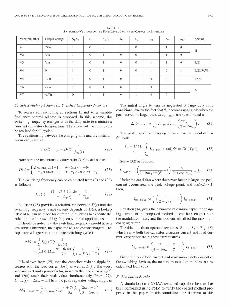
TABLE IIISWITCHING VECTORS OF THE FIVE-LEVEL SWITCHED-CAPACITOR INVERTER
D. Soft-Switching Scheme for Switched-Capacitor Inverters
To realize soft switching at Sections II and V, a variablefrequency control scheme is proposed. In this scheme, theswitching frequency changes with the duty ratio to maintain aconstant capacitor charging time. Therefore, soft switching canbe realized for all cycles.
The relationship between the charging time and the instanta-neous duty ratio is
Tch(t) = (1−D(t))1
fsw(t). (26)
Note here the instantaneous duty ratio D(t) is defined as
D(t)=
{2ma sin(ωt)−1, θ1<ωt<π−θ1−2ma sin(ωt)−1, π+θ1<ωt<2π−θ1.
(27)
The switching frequency can be calculated from (8) and (26)as follows:
fsw(t) =(1−D(t))× 2π
π + θ0(t)× 1
Tosc. (28)
Equation (28) provides a relationship between D(t) and theswitching frequency. Since θ0 only depends on D(t), a lookuptable of θ0 can be made for different duty ratios to expedite thecalculation of the switching frequency in real applications.
It should be noted that the switching frequency should have alow limit. Otherwise, the capacitor will be overdischarged. Thecapacitor voltage variation in one switching cycle is
ΔVC =1
CId(t)D(t)
1
fsw(t)
=1
CId(t)Tosc
π + θ0(t)
2π
(1
1−D(t)− 1
). (29)
It is shown from (29) that the capacitor voltage ripple in-creases with the load current Id(t) as well as D(t). The worstscenario is at unity power factor, in which the load current Id(t)and D(t) reach their peak value simultaneously. From (27),Dmax(t) = 2ma − 1. Then, the peak capacitor voltage ripple is
ΔVC_max =1
CId_peakTosc
π + θ0(t)
2π
(2ma − 1
2− 2ma
). (30)
The initial angle θ0 can be neglected at large duty ratioconditions, due to the fact that θ0 becomes negligible when thepeak current is large; then, ΔVC_max can be estimated as
ΔVC_max ≈ 1
2CId_peakTosc
(2ma − 1
2− 2ma
). (31)
The peak capacitor charging current can be calculated asfollows:
(1−D(t))
π
π∫−θ0
Ich_peak sin(θ)dθ = D(t)Id(t). (32)
Solve (32) as follows:
Ich_peak=
(1
2−2ma sin(θ)−1
)π
(1+cos(θ0))Id(t). (33)
Under the condition where the power factor is large, the peakcurrent occurs near the peak voltage point, and cos(θ0) ≈ 1;then,
Ich_peak ≈ π
2
(1
2− 2ma− 1
)Id_peak. (34)
Equation (34) gives the estimated maximum capacitor charg-ing current of the proposed method. It can be seen that boththe modulation index and the load current affect the maximumcharging current.
The third-quadrant operated switches (S1 and S4 in Fig. 12),which carry both the capacitor charging current and load cur-rent, experience the highest current stress
IS1_peak ≈(
π
4− 4ma− π
2+ 1
)Id_peak. (35)
Given the peak load current and maximum safety current ofthe switching devices, the maximum modulation index can becalculated from (35).
E. Simulation Results
A simulation on a 20-kVA switched-capacitor inverter hasbeen performed using PSIM to verify the control method pro-posed in this paper. In this simulation, the dc input of this

1606 IEEE TRANSACTIONS ON INDUSTRY APPLICATIONS, VOL. 48, NO. 5, SEPTEMBER/OCTOBER 2012
Fig. 14. Simulation results of the inverter.
Fig. 15. Frequency spectrum of the output voltage.
inverter is 300 V, and the modulation index is 0.8. The loadis a constant RL load with resistance of 2 Ω and inductanceof 3.5 mH. The power factor of this converter is 0.83. Torealize soft switching at around 20 kHz, the loop inductanceis selected to be 200 nH, and the capacitance of the capacitoris 300 μF.
Fig. 14 shows the output voltage, output current, the currentof S2, and the switching frequency. It can be seen that, theswitching frequency is kept constant at 20 kHz in Sections I,III, IV, and VI. In Sections II and V, where capacitor chargingoccurs, the switching frequency varies from 15 to 25 kHz. Thepeak current of S2 is about 426 A, whereas the peak load currentis 197 A. This ratio of peak charging current over peak loadcurrent is 2.16, which is consistent with the estimated value of2.36 from (34).
Fig. 15 shows the frequency spectrum of the output voltage.Because of the variable frequency control, there is a band offrequency components between 15 and 25 kHz.
V. EXPERIMENTAL RESULTS
A group of 1-kW half-cell prototypes has been built to verifythe ideas presented in this paper. The photograph of this cellis shown in Fig. 16. Three MOSFETs (IRFI4410ZPbF) areplaced in parallel to form one switching device. To reduce the
Fig. 16. Photograph of the prototype cell.
Fig. 17. Input and output voltage waveform of the voltage doubler.
reverse recovery loss of the body diode, a power Schottky diode(STPS30100ST) is used. Ten 100-V 4.7-μF ceramic capacitors(C5750X7R2A475K) are used together as the main capacitor.The soft-switching frequency of a voltage doubler is measuredat an input voltage of 5 V and room temperature. When theswitching frequency is adjusted to 62.7 kHz, the zero-currentturn-off is achieved. With the assumption that the capacitanceof the capacitor under this test condition is 47 μF, the total loopstray inductance can be calculated as 117.6 nH.
A. DC–DC Multiplier Test
A half-cell dc–dc voltage doubler, which consists of twoprototype boards, is used to verify the soft-switching schemeand the efficiency. The circuit topology is shown in Fig. 4. Thedead time is set to be 200 ns. A small 10-μF film capacitoris added to the output terminal to filter out the ripples duringthe dead time. At an input voltage of 40 V, the zero-currentturn-off is achieved for S1 and S5 at a switching frequency of75.9 kHz. Compared with the case when the input voltage is5 V, the soft-switching frequency is increased, which is becausethe capacitance of the ceramic capacitors decreases with theincrease in voltage.
Fig. 17 shows the input and output voltage together at aload current of 10 A. Fig. 18 shows with the drain–sourcevoltage Vs1 and the drain current IS1 of S1. It can be seen thatIS1 drops to zero before the switching transient; therefore, the
ZOU et al.: SWITCHED-CAPACITOR-CELL-BASED VOLTAGE MULTIPLIERS AND DC–AC INVERTERS 1607
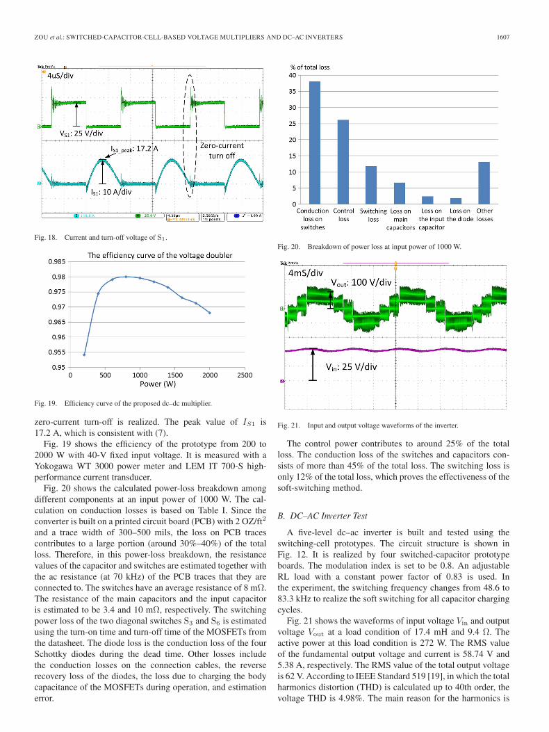
Fig. 18. Current and turn-off voltage of S1.
Fig. 19. Efficiency curve of the proposed dc–dc multiplier.
zero-current turn-off is realized. The peak value of IS1 is17.2 A, which is consistent with (7).
Fig. 19 shows the efficiency of the prototype from 200 to2000 W with 40-V fixed input voltage. It is measured with aYokogawa WT 3000 power meter and LEM IT 700-S high-performance current transducer.
Fig. 20 shows the calculated power-loss breakdown amongdifferent components at an input power of 1000 W. The cal-culation on conduction losses is based on Table I. Since theconverter is built on a printed circuit board (PCB) with 2 OZ/ft2
and a trace width of 300–500 mils, the loss on PCB tracescontributes to a large portion (around 30%–40%) of the totalloss. Therefore, in this power-loss breakdown, the resistancevalues of the capacitor and switches are estimated together withthe ac resistance (at 70 kHz) of the PCB traces that they areconnected to. The switches have an average resistance of 8 mΩ.The resistance of the main capacitors and the input capacitoris estimated to be 3.4 and 10 mΩ, respectively. The switchingpower loss of the two diagonal switches S3 and S6 is estimatedusing the turn-on time and turn-off time of the MOSFETs fromthe datasheet. The diode loss is the conduction loss of the fourSchottky diodes during the dead time. Other losses includethe conduction losses on the connection cables, the reverserecovery loss of the diodes, the loss due to charging the bodycapacitance of the MOSFETs during operation, and estimationerror.
Fig. 20. Breakdown of power loss at input power of 1000 W.
Fig. 21. Input and output voltage waveforms of the inverter.
The control power contributes to around 25% of the totalloss. The conduction loss of the switches and capacitors con-sists of more than 45% of the total loss. The switching loss isonly 12% of the total loss, which proves the effectiveness of thesoft-switching method.
B. DC–AC Inverter Test
A five-level dc–ac inverter is built and tested using theswitching-cell prototypes. The circuit structure is shown inFig. 12. It is realized by four switched-capacitor prototypeboards. The modulation index is set to be 0.8. An adjustableRL load with a constant power factor of 0.83 is used. Inthe experiment, the switching frequency changes from 48.6 to83.3 kHz to realize the soft switching for all capacitor chargingcycles.
Fig. 21 shows the waveforms of input voltage Vin and outputvoltage Vout at a load condition of 17.4 mH and 9.4 Ω. Theactive power at this load condition is 272 W. The RMS valueof the fundamental output voltage and current is 58.74 V and5.38 A, respectively. The RMS value of the total output voltageis 62 V. According to IEEE Standard 519 [19], in which the totalharmonics distortion (THD) is calculated up to 40th order, thevoltage THD is 4.98%. The main reason for the harmonics is

1608 IEEE TRANSACTIONS ON INDUSTRY APPLICATIONS, VOL. 48, NO. 5, SEPTEMBER/OCTOBER 2012
Fig. 22. Waveforms of the output current Id and the charging current IC1.
Fig. 23. Zoomed-in capacitor charging current of the inverter.
the large stray inductance of the current paths when the inverterfunctions as an H-bridge inverter. This occurs because fouridentical prototype boards are connected using external cablesin this experiment, and unnecessary large inductance is presenteven if the capacitor charging is not required. An integratedinverter design can help to optimize the stray inductance dis-tribution and solve this problem.
Fig. 22 shows the waveforms of load current Id and thecharging current of capacitor C1. The peak value of IC1 is21 A, whereas the peak value of Id is 9 A. The ratio between thetwo peak values is 2.33, which is consistent with the estimationresult of (34).
Fig. 23 shows the zoomed-in view of the capacitor chargingcurrent of C1. It can be seen that the zero-current switching isrealized for all cycles.
Fig. 24 shows the efficiency curve of the proposed dc–acinverter with an input power from 100 to 1000 W. The efficiencyvalue is about 3% lower than the efficiency of the voltagedoubler. The main reason is that four extra switching devicesare involved in the inverter topology, which introduce moreconduction loss and control power loss. In addition, the peakvalue of the charging current of the inverter is higher thanthat of the voltage doubler, which generates higher conductionloss.
Fig. 24. Efficiency curve of the proposed dc–ac inverter.
VI. CONCLUSION
This paper introduced two types of switched-capacitor cells:the half-cell and the full cell. Both the dc–dc multipliers andthe dc–ac inverters based on these cells are analyzed. For thedc–dc multiplier, a rotational charging scheme is proposed;therefore, the large output capacitor required by traditionalswitched-capacitor topologies can be eliminated. For the dc–acinversion, a multilevel inverter with voltage boost function canbe realized by using either the full cell or the half-cell. Toincrease the efficiency, a soft-switching scheme without addingextra components is adopted, and a variable frequency controlfor the inverter is proposed to realize full-range soft switching.The proposed topologies and control methods can be used inapplications with a power range from subkilowatts to tens ofkilowatts.
REFERENCES
[1] A. Ioinovici, “Switched-capacitor power electronics circuits,” IEEECircuits Syst. Mag., vol. 1, no. 3, pp. 37–42, Third Quarter, 2001.
[2] H. Chung, “Design and analysis of a switched-capacitor-based step-updc/dc converter with continuous input current,” IEEE Trans. Circuits Syst.I, Fundam. Theory Appl., vol. 46, no. 6, pp. 722–730, Jun. 1999.
[3] H. S. Chung, A. Ioinovici, and W. Cheung, “Generalized structure of bidi-rectional switched-capacitor DC/DC converters,” IEEE Trans. CircuitsSyst. I, Fundam. Theory Appl., vol. 50, no. 6, pp. 743–753, Jun. 2003.
[4] F. L. Luo and H. Ye, “Positive output multiple-lift push-pull switched-capacitor Luo-converters,” IEEE Trans. Ind. Electron., vol. 51, no. 3,pp. 594–602, Jun. 2004.
[5] B. Arntzen and D. Maksimovic, “Switched-capacitor DC/DC converterswith resonant gate drive,” IEEE Trans. Power Electron., vol. 13, no. 5,pp. 892–902, Sep. 1998.
[6] F. Z. Peng, F. Zhang, and Z. Qian, “A magnetic-less DC-DC converter fordual-voltage automotive systems,” IEEE Trans. Ind. Appl., vol. 39, no. 2,pp. 511–518, Mar./Apr. 2003.
[7] W. Qian, F. Z. Peng, and L. M. Tolbert, “Development of a 55 kW 3XDC-DC converter for HEV systems,” in Proc. Veh. Power PropulsionConf., 2009, pp. 433–439.
[8] F. H. Khan and L. M. Tolbert, “A multilevel modular capacitor-clampedDC-DC converter,” IEEE Trans. Ind. Appl., vol. 43, no. 6, pp. 1628–1638,Nov./Dec. 2007.
[9] K. K. Law, K. W. E. Cheng, and Y. P. B. Yeung, “Design and analysisof switched-capacitor-based step-up resonant converters,” IEEE Trans.Circuits Syst. I, Reg. Papers, vol. 52, no. 5, pp. 943–948, May 2005.
[10] M. Shoyama, F. Deriha, and T. Ninomiya, “Operation analysis and controlof resonant boost switched capacitor converter with high efficiency,” inProc. Power Electron. Spec. Conf., 2005, pp. 1966–1971.
[11] J. Kimball, P. Krein, and K. Cahill, “Modeling of capacitor impedance inswitching converters,” IEEE Power Electron. Lett., vol. 3, no. 4, pp. 136–140, Dec. 2005.
ZOU et al.: SWITCHED-CAPACITOR-CELL-BASED VOLTAGE MULTIPLIERS AND DC–AC INVERTERS 1609
[12] D. Cao and F. Z. Peng, “A family of zero current switching switched-capacitor DC-DC converters,” in Proc. 25th Annu. IEEE APEC,Feb. 21–25, 2010, pp. 1365–1372.
[13] D. Cao and F. Z. Peng, “Zero-current-switching multilevel modularswitched-capacitor DC-DC converter,” IEEE Trans. Ind. Appl., vol. 46,no. 6, pp. 2536–2544, Nov./Dec. 2010.
[14] D. Cao and F. Z. Peng, “Multiphase multilevel modular DC-DC converterfor high current high gain TEG application,” in Proc. IEEE Energy Con-vers. Congr. Expo., Atlanta, GA, 2010, pp. 4230–4237.
[15] J. I. Rodriguez and S. B. Leeb, “A multilevel inverter topology for in-ductively coupled power transfer,” IEEE Trans. Power Electron., vol. 21,no. 6, pp. 1607–1617, Nov. 2006.
[16] F. Zhang, S. Yang, F. Z. Peng, and Z. Qian, “A zigzag cascaded multilevelinverter topology with self voltage balancing,” in Proc. IEEE APEC, Feb.2008, pp. 1632–1635.
[17] O. Mak and A. Ioinovici, “Switched-capacitor inverter with high powerdensity and enhanced regulation capability,” IEEE Trans. Circuits Syst. I,Fundam. Theory Appl., vol. 45, no. 4, pp. 336–348, Jun. 1998.
[18] Y. Chang, “Design and analysis of multistage multiphase switched-capacitor boost DC-AC inverter,” IEEE Trans. Circuits Syst. I, Reg.Papers, vol. 58, no. 1, pp. 205–218, Jan. 2011.
[19] IEEE Recommended Practice and Requirements for Harmonic Control inElectric Power Systems, IEEE Std. 519-1992.
Ke Zou (S’09) received the B.S. and M.S. degreesfrom Xi‘an Jiaotong University, Xi’an, China, in2005 and 2008, respectively. He is currently workingtoward the Ph.D. degree at The Ohio State Univer-sity, Columbus.
His current research interests include switched-capacitor dc/dc converters and dc/ac multilevelinverters, battery models in high-frequency applica-tions, and hardware-in-the-loop systems for powerelectronics and power systems.
Mark J. Scott (S’09) received the B.S. degree inelectrical and computer engineering from The OhioState University, Columbus, in 2005. He is currentlyworking toward the Ph.D. degree in electrical andcomputer engineering at The Ohio State University.
He has worked as a Field Engineer installinglarge industrial automated systems and as a TestEngineer validating power electronics for automo-tive applications. His research interests include uti-lizing wide-band-gap devices in new and existingpower electronic topologies for renewable energy
applications.Mr. Scott is the founding member of the IEEE Graduate Student Body at The
Ohio State University and a member of Tau Beta Pi.
Jin Wang (S’02–M’05) received the B.S. degreefrom Xi’an Jiaotong University, Xi’an, China, in1998, the M.S. degree from Wuhan University,Wuhan, China, in 2001, and the Ph.D. degree fromMichigan State University, East Lansing, MI, in2005, all in electrical engineering.
From September 2005 to August 2007, he workedat the Ford Motor Company as a Core Power Elec-tronics Engineer and contributed to the traction drivedesign of the Ford Fusion Hybrid. Since September2007, he has been an Assistant Professor in the De-
partment of Electrical and Computer Engineering, The Ohio State University,Columbus. His teaching position is cosponsored by American Electric Power,Duke/Synergy, and FirstEnergy. He is the author of 40 peer-reviewed journaland conference publications. His research interests include high-voltage andhigh-power converter/inverters, integration of renewable energy sources, andelectrification of transportation.
Dr. Wang was the recipient of the IEEE Power Electronics Society RichardM. Bass Young Engineer Award and the National Science Foundation’sCAREER Award, both in 2011. Since March 2008, he has been an AssociateEditor for the IEEE TRANSACTIONS ON INDUSTRY APPLICATION.