lm97593 dual adc / digital tuner / agc (rev. b) - ti. · pdf filethe lm97593 dual adc /...
TRANSCRIPT
LM97593
www.ti.com SNWS019B –JULY 2007–REVISED APRIL 2013
LM97593 Dual ADC / Digital Tuner / AGCCheck for Samples: LM97593
1FEATURES DESCRIPTIONThe LM97593 Dual ADC / Digital Tuner / AGC IC is a
2• 100% Software Compatible with the CLC5903two channel digital downconverter (DDC) with
• Pin Compatible with the CLC5903 Except for integrated 12-bit analog-to-digital converters (ADCs)the Analog Input and Reference Section and automatic gain control (AGC). The LM97593
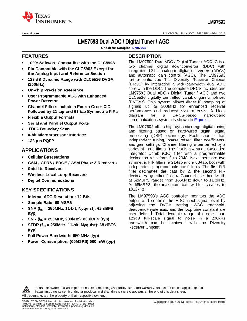
• 123 dB Dynamic Range with CLC5526 DVGA further enhances TI’s Diversity Receiver Chipset(DRCS) by integrating a wide-bandwidth dual ADC(200kHz)core with the DDC. The complete DRCS includes one• On-chip Precision ReferenceLM97593 Dual ADC / Digital Tuner / AGC and two
• User Programmable AGC with Enhanced CLC5526 digitally controlled variable gain amplifiersPower Detector (DVGAs). This system allows direct IF sampling of
signals up to 300MHz for enhanced receiver• Channel Filters Include a Fourth Order CICperformance and reduced system costs. A blockFollowed by 21-tap and 63-tap Symmetric FIRsdiagram for a DRCS-based narrowband• Flexible Output Formatscommunications system is shown in Figure 1.
• Serial and Parallel Output PortsThe LM97593 offers high dynamic range digital tuning
• JTAG Boundary Scan and filtering based on hard-wired digital signal• 8-bit Microprocessor Interface processing (DSP) technology. Each channel has
independent tuning, phase offset, filter coefficients,• 128 pin PQFPand gain settings. Channel filtering is performed by aseries of three filters. The first is a 4-stage CascadedAPPLICATIONSIntegrator Comb (CIC) filter with a programmable
• Cellular Basestations decimation ratio from 8 to 2048. Next there are twosymmetric FIR filters, a 21-tap and a 63-tap, both with• GSM / GPRS / EDGE / GSM Phase 2 Receiversindependent programmable coefficients. The first FIR• Satellite Receiversfilter decimates the data by 2, the second FIR
• Wireless Local Loop Receivers decimates by either 2 or 4. Channel filter bandwidthat 52MSPS ranges from ±650kHz down to ±1.3kHz.• Digital CommunicationsAt 65MSPS, the maximum bandwidth increases to±812kHz.KEY SPECIFICATIONSThe LM97593’s AGC controller monitors the ADC• Internal ADC Resolution: 12 Bitsoutput and controls the ADC input signal level by• Sample Rate: 65 MSPSadjusting the DVGA setting. AGC threshold,
• SNR (fIN = 250MHz, 11-bit, Nyquist): 62 dBFS deadband+hysteresis, and the loop time constant are(typ) user defined. Total dynamic range of greater than
123dB full-scale signal to noise in a 200kHz• SNR (fIN = 250MHz, 200kHz): 83 dBFS (typ)bandwidth can be achieved with the Diversity• SFDR (fIN = 250MHz, 11-bit, Nyquist): 68 dBFS Receiver Chipset.
(typ)• Full Power Bandwidth: 650 MHz (typ)• Power Consumption: (65MSPS) 560 mW (typ)
1
Please be aware that an important notice concerning availability, standard warranty, and use in critical applications ofTexas Instruments semiconductor products and disclaimers thereto appears at the end of this data sheet.
2All trademarks are the property of their respective owners.
PRODUCTION DATA information is current as of publication date. Copyright © 2007–2013, Texas Instruments IncorporatedProducts conform to specifications per the terms of the TexasInstruments standard warranty. Production processing does notnecessarily include testing of all parameters.
BGAIN[2]
A[5]
VDR
D18GND
BGAIN[0]
BGAIN[1]
~BSTROBE
D18GND
~MR
~SI
DRGND
A[7]
VD18
A[4]
A[3]
A[2]
A[1]
A[0]
~WR
~RD
~CE
D[7]
D[6]
VDR
A[6]
AGAIN[2]
VD18
VDR
TDO
AGAIN[0]
AGAIN[1]
~ASTROBE
VD18~SCAN_EN
~TRST
D18GND
TCK
TMS
POUT_SEL[0]
POUT_SEL[1]
POUT_SEL[2]
~POUT_EN
DRGND
POUT[0]
POUT[1]
VDR
POUT[3]
POUT[2]
POUT[4]
D18GND
TDI
CK
VA
VD
R
VIN
B+
NC
NC
VD
DG
ND
DG
ND
VD
PD
VA
AG
ND
VC
OM
B
VR
PB
VR
NB
VR
EF
AG
ND
VA
AG
ND
VR
NA
VC
OM
A
VR
PA
VIN
A+
VIN
A-
VIN
B-
VA
AG
ND
AG
ND
VA
RE
FS
EL/
DC
S
DG
ND
VD
DG
ND
VD
NC
AG
ND
DR
GN
D
LM97593VHDual Digital Tuner / AGC / ADC
(Top View)
D18
GN
D
BO
UT
D18
GN
D
RD
Y
DR
GN
D
NC
D[5
]
D[4
]
D[3
]
D[2
]
D[1
]
VD
18D
[0]
VD
RS
CK
SF
S
AO
UT
DR
GN
D
PO
UT
[15]
VD
18P
OU
T[1
4]
PO
UT
[12]
PO
UT
[13]
DR
GN
D
PO
UT
[11]
D18
GN
D
VD
R
PO
UT
[10]
PO
UT
[8]
PO
UT
[9]
PO
UT
[7]
PO
UT
[6]
PO
UT
[5]
DR
GN
D
SC
K_I
N
NC
NC
VD
R
DRGND
40
52
39
51
42
41
43
44
45
46
47
48
49
53
54
55
56
57
58
59
60
62
61
63
64
50
127
115
128
116
125
126
124
123
122
121
120
119
118
114
113
112
111
110
109
108
107
105
106
104
103
117
66 7865 776867 69 70 71 72 73 74 75 79 80 81 82 83 84 85 86 8887 89 9076 9291 9493 95 96 97 98 99 100
101
102
37 2538 263536 34 33 32 31 30 29 28 24 23 22 21 20 19 18 17 1516 14 1327 1112 910 8 7 6 5 4 3 2 1
DVGAIF ASerialOutA/B
SerialOutBSCK
SFS
RDY
LC
DVGAIF B
LCParallelOutput[15:0]
ParallelOutputEnable
ParallelSelect[2:0]
CLC5526
CLK
12
8
12ADC
SCK_IN
Dual DigitalTuner/AGC
LM97593
(x2)
ADC
LM97593
SNWS019B –JULY 2007–REVISED APRIL 2013 www.ti.com
Block Diagram 1
Figure 1. Diversity Receiver Chipset Block Diagram
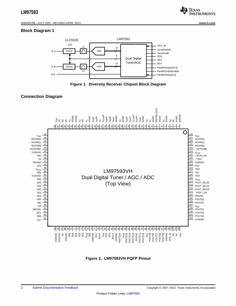
Connection Diagram
Figure 2. LM97593VH PQFP Pinout
2 Submit Documentation Feedback Copyright © 2007–2013, Texas Instruments Incorporated
Product Folder Links: LM97593
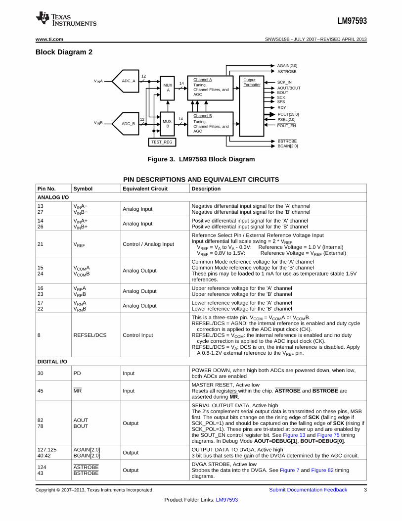
ADC_A
ADC_B
MUX
MUX
AOUT/BOUTBOUTSCKSFS
RDY
POUT[15:0]PSEL[2:0]
POUT_EN
ASTROBE
BGAIN[2:0]BSTROBE
14
14
A
B
Channel ASCK_IN
TEST_REG
Channel B
12
12
OutputFormatter
AGAIN[2:0]
Tuning,Channel Filters, andAGC
Tuning,Channel Filters, andAGC
VINA
VINB
LM97593
www.ti.com SNWS019B –JULY 2007–REVISED APRIL 2013
Block Diagram 2
Figure 3. LM97593 Block Diagram
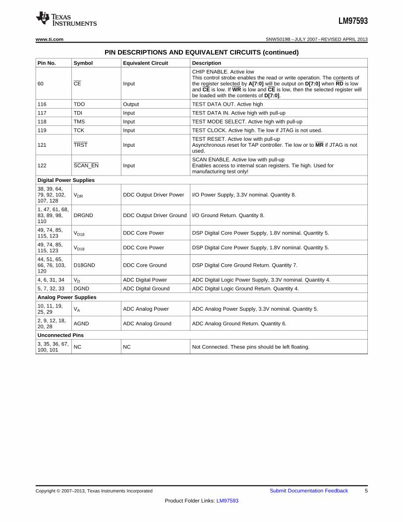
PIN DESCRIPTIONS AND EQUIVALENT CIRCUITSPin No. Symbol Equivalent Circuit Description
ANALOG I/O
13 VINA− Negative differential input signal for the 'A' channelAnalog Input27 VINB− Negative differential input signal for the 'B' channel
14 VINA+ Positive differential input signal for the 'A' channelAnalog Input26 VINB+ Positive differential input signal for the 'B' channel
Reference Select Pin / External Reference Voltage InputInput differential full scale swing = 2 * VREF21 VREF Control / Analog Input VREF = VA to VA - 0.3V: Reference Voltage = 1.0 V (Internal)
VREF = 0.8V to 1.5V: Reference Voltage = VREF (External)
Common Mode reference voltage for the 'A' channel15 VCOMA Common Mode reference voltage for the 'B' channelAnalog Output24 VCOMB These pins may be loaded to 1 mA for use as temperature stable 1.5V
references.
16 VRPA Upper reference voltage for the 'A' channelAnalog Output23 VRPB Upper reference voltage for the 'B' channel
17 VRNA Lower reference voltage for the 'A' channelAnalog Output22 VRNB Lower reference voltage for the 'B' channel
This is a three-state pin. VCOM = VCOMA or VCOMB.REFSEL/DCS = AGND: the internal reference is enabled and duty cycle
correction is applied to the ADC input clock (CK).8 REFSEL/DCS Control Input REFSEL/DCS = VCOM: the internal reference is enabled and no duty
cycle correction is applied to the ADC input clock (CK).REFSEL/DCS = VA: DCS is on, the internal reference is disabled. Apply
A 0.8-1.2V external reference to the VREF pin.
DIGITAL I/O
POWER DOWN, when high both ADCs are powered down, when low,30 PD Input both ADCs are enabled
MASTER RESET, Active low45 MR Input Resets all registers within the chip. ASTROBE and BSTROBE are
asserted during MR.
SERIAL OUTPUT DATA, Active highThe 2's complement serial output data is transmitted on these pins, MSBfirst. The output bits change on the rising edge of SCK (falling edge if82 AOUT Output SCK_POL=1) and should be captured on the falling edge of SCK (rising if78 BOUT SCK_POL=1). These pins are tri-stated at power up and are enabled bythe SOUT_EN control register bit. See Figure 13 and Figure 75 timingdiagrams. In Debug Mode AOUT=DEBUG[1], BOUT=DEBUG[0].
127:125 AGAIN[2:0] OUTPUT DATA TO DVGA, Active highOutput40:42 BGAIN[2:0] 3 bit bus that sets the gain of the DVGA determined by the AGC circuit.
DVGA STROBE, Active low124 ASTROBE Output Strobes the data into the DVGA. See Figure 7 and Figure 82 timing43 BSTROBE diagrams.
Copyright © 2007–2013, Texas Instruments Incorporated Submit Documentation Feedback 3
Product Folder Links: LM97593
LM97593
SNWS019B –JULY 2007–REVISED APRIL 2013 www.ti.com
PIN DESCRIPTIONS AND EQUIVALENT CIRCUITS (continued)
Pin No. Symbol Equivalent Circuit Description
SERIAL DATA CLOCK, Active high or lowThe serial data is clocked out of the chip by this clock. The active edge ofthe clock is user programmable. This pin is tri-stated at power up and is
80 SCK Output enabled by the SOUT_EN control register bit. See Figure 13 andFigure 75 timing diagrams. In Debug Mode outputs an appropiate clockfor the debug data. If RATE=0 the input CK duty cycle will be reflected toSCK.
SERIAL DATA CLOCK INPUT, Active high or lowData bits from a serial daisy-chain slave are clocked into a serial daisy-99 SCK_IN Input chain master on the falling edge of SCK_IN (rising if SCK_POL=1 on theslave). Tie low if not used.
SERIAL FRAME STROBE, Active high or lowThe serial word strobe. This strobe delineates the words within the serialoutput streams. This strobe is a pulse at the beginning of each serial
81 SFS Output word (PACKED=0) or each serial word I/Q pair (PACKED=1). The polarityof this signal is user programmable. This pin is tri-stated at power up andis enabled by the SOUT_EN control register bit. See Figure 13 andFigure 75 timing diagrams. In Debug Mode SFS=DEBUG[2].
84, 86:88, PARALLEL OUTPUT DATA, Active high90, 91, The output data is transmitted on these pins in parallel format. The93:97, POUT[15:0] Output POUT_SEL[2:0] pins select one of eight 16-bit output words. The104:106, POUT_EN pin enables these outputs. POUT[15] is the MSB. In Debug108, 109 Mode POUT[15:0]=DEBUG[19:4].
PARALLEL OUTPUT DATA SELECT, Active highThe 16-bit output word is selected with these 3 pins. Not used in Debug
112:114 POUT_SEL[2:0] Input Mode. For a serial daisy-chain master, POUT_SEL[2:0] become inputsfrom the slave: POUT_SEL[2]=SFSSLAVE, POUT_SEL[1]=BOUTSLAVE,and POUT_SEL[0]=AOUTSLAVE. Tie low if not used.
PARALLEL OUTPUT ENABLE. Active low111 POUT_EN Input This pin enables the chip to output the selected output word on the
POUT[15:0] pins. Not used in Debug Mode. Tie high if not used.
READY FLAG, Active high or lowThe chip asserts this signal to identify the beginning of an output sampleperiod (OSP). The polarity of this signal is user programmable. This77 RDY Output signal is typically used as an interrupt to a DSP chip, but can also beused as a start pulse to dedicated circuitry. This pin is active regardlessof the state of SOUT_EN. In Debug Mode RDY=DEBUG[3].
INPUT CLOCK. Active highThe clock input to the chip. The The VINA and VINB analog input signals37 CK Input are sampled on the rising edge of this signal. SI is clocked into the chipon the rising edge of CK.
SYNC IN. Active lowThe sync input to the chip. The decimation counters, dither, and NCOphase can be synchronized by SI. This sync is clocked into the chip on46 SI Input the rising edge of CK. Tie this pin high if external sync is not required. Allsample data is flushed by SI. To properly initialize the DVGA ASTROBEand BSTROBE are asserted during SI.
DATA BUS. Active high62, 63, This is the 8 bit control data I/O bus. Control register data is loaded intoD[7:0] Input/Output69:73, 75 the chip or read from the chip through these pins. The chip will only drive
output data on these pins when CE is low, RD is low, and WR is high.
ADDRESS BUS. Active highThese pins are used to address the control registers within the chip. Each
48, 50, 52:57 A[7:0] Input of the control registers within the chip are assigned a unique address. Acontrol register can be written to or read from by setting A[7:0] to theregister’s address and setting CE, RD, and WR appropriately.
READ ENABLE. Active low59 RD Input This pin enables the chip to output the contents of the selected register
on the D[7:0] pins when CE is also low.
WRITE ENABLE. Active lowThis pin enables the chip to write the value on the D[7:0] pins into the58 WR Input selected register when CE is also low. This pin can also function as RD/CE if RD is held low. See Figure 15 for details.
4 Submit Documentation Feedback Copyright © 2007–2013, Texas Instruments Incorporated
Product Folder Links: LM97593
LM97593
www.ti.com SNWS019B –JULY 2007–REVISED APRIL 2013
PIN DESCRIPTIONS AND EQUIVALENT CIRCUITS (continued)
Pin No. Symbol Equivalent Circuit Description
CHIP ENABLE. Active lowThis control strobe enables the read or write operation. The contents of
60 CE Input the register selected by A[7:0] will be output on D[7:0] when RD is lowand CE is low. If WR is low and CE is low, then the selected register willbe loaded with the contents of D[7:0].
116 TDO Output TEST DATA OUT. Active high
117 TDI Input TEST DATA IN. Active high with pull-up
118 TMS Input TEST MODE SELECT. Active high with pull-up
119 TCK Input TEST CLOCK. Active high. Tie low if JTAG is not used.
TEST RESET. Active low with pull-up121 TRST Input Asynchronous reset for TAP controller. Tie low or to MR if JTAG is not
used.
SCAN ENABLE. Active low with pull-up122 SCAN_EN Input Enables access to internal scan registers. Tie high. Used for
manufacturing test only!
Digital Power Supplies
38, 39, 64,79, 92, 102, VDR DDC Output Driver Power I/O Power Supply, 3.3V nominal. Quantity 8.107, 128
1, 47, 61, 68,83, 89, 98, DRGND DDC Output Driver Ground I/O Ground Return. Quantity 8.110
49, 74, 85, VD18 DDC Core Power DSP Digital Core Power Supply, 1.8V nominal. Quantity 5.115, 123
49, 74, 85, VD18 DDC Core Power DSP Digital Core Power Supply, 1.8V nominal. Quantity 5.115, 123
44, 51, 65,66, 76, 103, D18GND DDC Core Ground DSP Digital Core Ground Return. Quantity 7.120
4, 6, 31, 34 VD ADC Digital Power ADC Digital Logic Power Supply, 3.3V nominal. Quantity 4.
5, 7, 32, 33 DGND ADC Digital Ground ADC Digital Logic Ground Return. Quantity 4.
Analog Power Supplies
10, 11, 19, VA ADC Analog Power ADC Analog Power Supply, 3.3V nominal. Quantity 5.25, 29
2, 9, 12, 18, AGND ADC Analog Ground ADC Analog Ground Return. Quantity 6.20, 28
Unconnected Pins
3, 35, 36, 67, NC NC Not Connected. These pins should be left floating.100, 101
Copyright © 2007–2013, Texas Instruments Incorporated Submit Documentation Feedback 5
Product Folder Links: LM97593
LM97593
SNWS019B –JULY 2007–REVISED APRIL 2013 www.ti.com
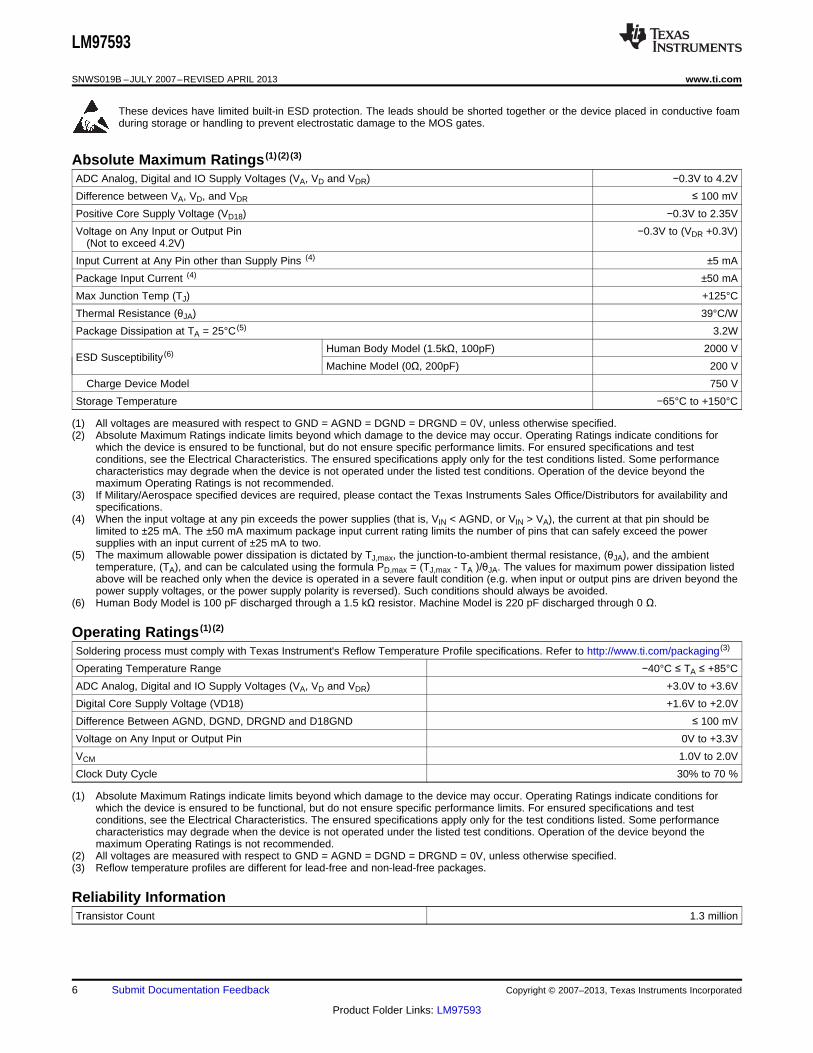
These devices have limited built-in ESD protection. The leads should be shorted together or the device placed in conductive foamduring storage or handling to prevent electrostatic damage to the MOS gates.
Absolute Maximum Ratings (1) (2) (3)
ADC Analog, Digital and IO Supply Voltages (VA, VD and VDR) −0.3V to 4.2V
Difference between VA, VD, and VDR ≤ 100 mV
Positive Core Supply Voltage (VD18) −0.3V to 2.35V
Voltage on Any Input or Output Pin −0.3V to (VDR +0.3V)(Not to exceed 4.2V)
Input Current at Any Pin other than Supply Pins (4) ±5 mA
Package Input Current (4) ±50 mA
Max Junction Temp (TJ) +125°C
Thermal Resistance (θJA) 39°C/W
Package Dissipation at TA = 25°C (5) 3.2W
Human Body Model (1.5kΩ, 100pF) 2000 VESD Susceptibility (6)
Machine Model (0Ω, 200pF) 200 V
Charge Device Model 750 V
Storage Temperature −65°C to +150°C
(1) All voltages are measured with respect to GND = AGND = DGND = DRGND = 0V, unless otherwise specified.(2) Absolute Maximum Ratings indicate limits beyond which damage to the device may occur. Operating Ratings indicate conditions for
which the device is ensured to be functional, but do not ensure specific performance limits. For ensured specifications and testconditions, see the Electrical Characteristics. The ensured specifications apply only for the test conditions listed. Some performancecharacteristics may degrade when the device is not operated under the listed test conditions. Operation of the device beyond themaximum Operating Ratings is not recommended.
(3) If Military/Aerospace specified devices are required, please contact the Texas Instruments Sales Office/Distributors for availability andspecifications.
(4) When the input voltage at any pin exceeds the power supplies (that is, VIN < AGND, or VIN > VA), the current at that pin should belimited to ±25 mA. The ±50 mA maximum package input current rating limits the number of pins that can safely exceed the powersupplies with an input current of ±25 mA to two.
(5) The maximum allowable power dissipation is dictated by TJ,max, the junction-to-ambient thermal resistance, (θJA), and the ambienttemperature, (TA), and can be calculated using the formula PD,max = (TJ,max - TA )/θJA. The values for maximum power dissipation listedabove will be reached only when the device is operated in a severe fault condition (e.g. when input or output pins are driven beyond thepower supply voltages, or the power supply polarity is reversed). Such conditions should always be avoided.
(6) Human Body Model is 100 pF discharged through a 1.5 kΩ resistor. Machine Model is 220 pF discharged through 0 Ω.
Operating Ratings (1) (2)
Soldering process must comply with Texas Instrument's Reflow Temperature Profile specifications. Refer to http://www.ti.com/packaging(3)
Operating Temperature Range −40°C ≤ TA ≤ +85°C
ADC Analog, Digital and IO Supply Voltages (VA, VD and VDR) +3.0V to +3.6V
Digital Core Supply Voltage (VD18) +1.6V to +2.0V
Difference Between AGND, DGND, DRGND and D18GND ≤ 100 mV
Voltage on Any Input or Output Pin 0V to +3.3V
VCM 1.0V to 2.0V
Clock Duty Cycle 30% to 70 %
(1) Absolute Maximum Ratings indicate limits beyond which damage to the device may occur. Operating Ratings indicate conditions forwhich the device is ensured to be functional, but do not ensure specific performance limits. For ensured specifications and testconditions, see the Electrical Characteristics. The ensured specifications apply only for the test conditions listed. Some performancecharacteristics may degrade when the device is not operated under the listed test conditions. Operation of the device beyond themaximum Operating Ratings is not recommended.
(2) All voltages are measured with respect to GND = AGND = DGND = DRGND = 0V, unless otherwise specified.(3) Reflow temperature profiles are different for lead-free and non-lead-free packages.
Reliability InformationTransistor Count 1.3 million
6 Submit Documentation Feedback Copyright © 2007–2013, Texas Instruments Incorporated
Product Folder Links: LM97593
LM97593
www.ti.com SNWS019B –JULY 2007–REVISED APRIL 2013
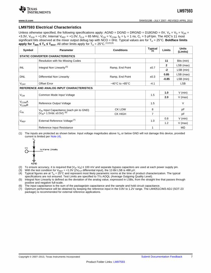
LM97593 Electrical CharacteristicsUnless otherwise specified, the following specifications apply: AGND = DGND = DRGND = D18GND = 0V, VA = VD = VDR =+3.3V, VD18 = +1.8V, Internal VREF = +1.0V, fCLK = 65 MHz, VCM = VCOM, tR = tF = 1 ns, CL = 5 pF/pin. The ADC’s 11 mostsignificant bits observed at the mixer output debug tap with NCO = 0Hz. Typical values are for TA = 25°C. Boldface limitsapply for TMIN ≤ TA ≤ TMAX. All other limits apply for TA = 25°C. (1) (2) (3)
Typical UnitsSymbol Parameter Conditions Limits(4) (Limits)
STATIC CONVERTER CHARACTERISTICS
Resolution with No Missing Codes 11 Bits (min)
2 LSB (max)INL Integral Non Linearity (5) Ramp, End Point ±0.7
-2 LSB (min)
0.85 LSB (max)DNL Differential Non Linearity Ramp, End Point ±0.3
-0.85 LSB (min)
VOFF Offset Error −40°C to +85°C -4.1 LSB
REFERENCE AND ANALOG INPUT CHARACTERISTICS
1.0 V (min)VCM Common Mode Input Voltage 1.5
2.0 V (max)
VCOMA Reference Output Voltage 1.5 VVCOMB
CK LOW 8 pFVIN Input Capacitance (each pin to GND)CIN (VIN= 1.5Vdc ±0.5V) (6)CK HIGH 7 pF
0.8 V (min)VREF External Reference Voltage (7) 1.0
1.2 V (max)
Reference Input Resistance 1 MΩ
(1) The inputs are protected as shown below. Input voltage magnitudes above VA or below GND will not damage this device, providedcurrent is limited per Note (4).
(2) To ensure accuracy, it is required that |VA–VD| ≤ 100 mV and separate bypass capacitors are used at each power supply pin.(3) With the test condition for VREF = +1.0V (2VP-P differential input), the 12-Bit LSB is 488 µV.(4) Typical figures are at TA = 25°C and represent most likely parametric norms at the time of product characterization. The typical
specifications are not ensured. Test Limits are specified to TI's AOQL (Average Outgoing Quality Level).(5) Integral Non Linearity is defined as the deviation of the analog value, expressed in LSBs, from the straight line that passes through
positive and negative full-scale.(6) The input capacitance is the sum of the package/pin capacitance and the sample and hold circuit capacitance.(7) Optimum performance will be obtained by keeping the reference input in the 0.8V to 1.2V range. The LM4051CIM3-ADJ (SOT-23
package) is recommended for external reference applications.
Copyright © 2007–2013, Texas Instruments Incorporated Submit Documentation Feedback 7
Product Folder Links: LM97593
LM97593
SNWS019B –JULY 2007–REVISED APRIL 2013 www.ti.com
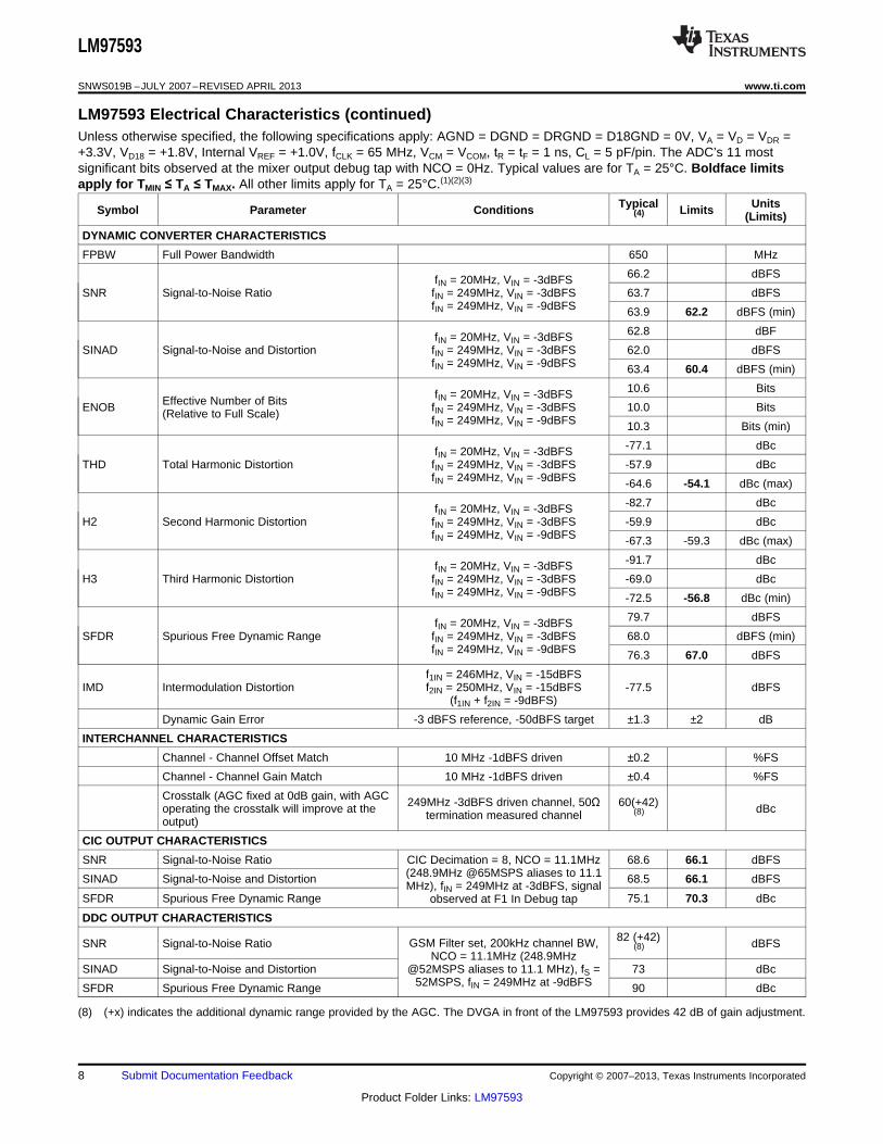
LM97593 Electrical Characteristics (continued)Unless otherwise specified, the following specifications apply: AGND = DGND = DRGND = D18GND = 0V, VA = VD = VDR =+3.3V, VD18 = +1.8V, Internal VREF = +1.0V, fCLK = 65 MHz, VCM = VCOM, tR = tF = 1 ns, CL = 5 pF/pin. The ADC’s 11 mostsignificant bits observed at the mixer output debug tap with NCO = 0Hz. Typical values are for TA = 25°C. Boldface limitsapply for TMIN ≤ TA ≤ TMAX. All other limits apply for TA = 25°C.(1)(2)(3)
Typical UnitsSymbol Parameter Conditions Limits(4) (Limits)
DYNAMIC CONVERTER CHARACTERISTICS
FPBW Full Power Bandwidth 650 MHz
66.2 dBFSfIN = 20MHz, VIN = -3dBFSSNR Signal-to-Noise Ratio fIN = 249MHz, VIN = -3dBFS 63.7 dBFS
fIN = 249MHz, VIN = -9dBFS 63.9 62.2 dBFS (min)
62.8 dBFfIN = 20MHz, VIN = -3dBFSSINAD Signal-to-Noise and Distortion fIN = 249MHz, VIN = -3dBFS 62.0 dBFS
fIN = 249MHz, VIN = -9dBFS 63.4 60.4 dBFS (min)
10.6 BitsfIN = 20MHz, VIN = -3dBFSEffective Number of BitsENOB fIN = 249MHz, VIN = -3dBFS 10.0 Bits(Relative to Full Scale) fIN = 249MHz, VIN = -9dBFS 10.3 Bits (min)
-77.1 dBcfIN = 20MHz, VIN = -3dBFSTHD Total Harmonic Distortion fIN = 249MHz, VIN = -3dBFS -57.9 dBc
fIN = 249MHz, VIN = -9dBFS -64.6 -54.1 dBc (max)
-82.7 dBcfIN = 20MHz, VIN = -3dBFSH2 Second Harmonic Distortion fIN = 249MHz, VIN = -3dBFS -59.9 dBc
fIN = 249MHz, VIN = -9dBFS -67.3 -59.3 dBc (max)
-91.7 dBcfIN = 20MHz, VIN = -3dBFSH3 Third Harmonic Distortion fIN = 249MHz, VIN = -3dBFS -69.0 dBc
fIN = 249MHz, VIN = -9dBFS -72.5 -56.8 dBc (min)
79.7 dBFSfIN = 20MHz, VIN = -3dBFSSFDR Spurious Free Dynamic Range fIN = 249MHz, VIN = -3dBFS 68.0 dBFS (min)
fIN = 249MHz, VIN = -9dBFS 76.3 67.0 dBFS
f1IN = 246MHz, VIN = -15dBFSIMD Intermodulation Distortion f2IN = 250MHz, VIN = -15dBFS -77.5 dBFS
(f1IN + f2IN = -9dBFS)
Dynamic Gain Error -3 dBFS reference, -50dBFS target ±1.3 ±2 dB
INTERCHANNEL CHARACTERISTICS
Channel - Channel Offset Match 10 MHz -1dBFS driven ±0.2 %FS
Channel - Channel Gain Match 10 MHz -1dBFS driven ±0.4 %FS
Crosstalk (AGC fixed at 0dB gain, with AGC 249MHz -3dBFS driven channel, 50Ω 60(+42)operating the crosstalk will improve at the dBctermination measured channel (8)output)
CIC OUTPUT CHARACTERISTICS
SNR Signal-to-Noise Ratio CIC Decimation = 8, NCO = 11.1MHz 68.6 66.1 dBFS(248.9MHz @65MSPS aliases to 11.1SINAD Signal-to-Noise and Distortion 68.5 66.1 dBFSMHz), fIN = 249MHz at -3dBFS, signal
SFDR Spurious Free Dynamic Range 75.1 70.3 dBcobserved at F1 In Debug tap
DDC OUTPUT CHARACTERISTICS
82 (+42)GSM Filter set, 200kHz channel BW,SNR Signal-to-Noise Ratio dBFS(8)NCO = 11.1MHz (248.9MHz
SINAD Signal-to-Noise and Distortion @52MSPS aliases to 11.1 MHz), fS = 73 dBc52MSPS, fIN = 249MHz at -9dBFSSFDR Spurious Free Dynamic Range 90 dBc
(8) (+x) indicates the additional dynamic range provided by the AGC. The DVGA in front of the LM97593 provides 42 dB of gain adjustment.
8 Submit Documentation Feedback Copyright © 2007–2013, Texas Instruments Incorporated
Product Folder Links: LM97593
LM97593
www.ti.com SNWS019B –JULY 2007–REVISED APRIL 2013
LM97593 Electrical Characteristics (continued)Unless otherwise specified, the following specifications apply: AGND = DGND = DRGND = D18GND = 0V, VA = VD = VDR =+3.3V, VD18 = +1.8V, Internal VREF = +1.0V, fCLK = 65 MHz, VCM = VCOM, tR = tF = 1 ns, CL = 5 pF/pin. The ADC’s 11 mostsignificant bits observed at the mixer output debug tap with NCO = 0Hz. Typical values are for TA = 25°C. Boldface limitsapply for TMIN ≤ TA ≤ TMAX. All other limits apply for TA = 25°C.(1)(2)(3)
Typical UnitsSymbol Parameter Conditions Limits(4) (Limits)
76 (+42)GSM Filter set, 200kHz channel BW,SNR Signal-to-Noise Ratio dBFS(9)NCO = 11.1MHz (248.9MHz
SINAD Signal-to-Noise and Distortion @52MSPS aliases to 11.1 MHz), fS = 74 dBc52MSPS, fIN = 249MHz at -3dBFSSFDR Spurious Free Dynamic Range 90 dBc
79 (+42)GSM Filter set, 200kHz channel BW,SNR Signal-to-Noise Ratio dBFS(9)NCO = 11.1MHz (248.9MHz
SINAD Signal-to-Noise and Distortion @65MSPS aliases to 11.1 MHz), fS = 71 dBc65MSPS, fIN = 249MHz at -9dBFSSFDR Spurious Free Dynamic Range 81 dBc
74 (+42)GSM Filter set, 200kHz channel BW,SNR Signal-to-Noise Ratio dBFS(9)NCO = 11.1MHz (248.9MHz
SINAD Signal-to-Noise and Distortion @65MSPS aliases to 11.1 MHz), fS = 71 dBc65MSPS, fIN = 249MHz at -3dBFSSFDR Spurious Free Dynamic Range 80 dBc
(9) (+x) indicates the additional dynamic range provided by the AGC. The DVGA in front of the LM97593 provides 42 dB of gain adjustment.
DC and Logic Electrical CharacteristicsUnless otherwise specified, the following specifications apply: AGND = DGND = DRGND = D18GND = 0V, VA = VD = VDR =+3.3V, VD18 = +1.8V, Internal VREF = +1.0V, fCLK = 65 MHz, VCM = VCOM, tR = tF = TBD ns, CL = 5 pF/pin. CIC Decimation = 48,F2 Decimation = 2. Typical values are for TA = 25°C. Boldface limits apply for TMIN ≤ TA ≤ TMAX. All other limits apply for TA
= 25°C.
Typical UnitsSymbol Parameter Conditions Limits(1) (Limits)
VIL Voltage input low 0.7 V (max)
VIH Voltage input high 2.3 V (min)
IOZ Input current 20 µA
VOL Voltage output low (IOL = 7mA) 0.4 V (max)
VOH Voltage output high (IOH = -7mA) 2.4 V (min)
CIN Input capacitance 5.0 pF
POWER SUPPLY CHARACTERISTICS
IA ADC Analog Supply Current 65MSPS 96 121 mA (max)
IA ADC Analog Supply Current 52MSPS 84 mA
ID ADC Digital Supply Current 65MSPS 24 28 mA (max)
ID ADC Digital Supply Current 52MSPS 20 mA
IDR Digital Output Supply Current (2) 65MSPS 14 18 mA (max)
IDR Digital Output Supply Current (2) 52MSPS 10 mA
ID18 Digital Core Supply Current 65MSPS 67 78 mA (max)
ID18 Digital Core Supply Current 52MSPS 53 mA
PD65 Total Power Dissipation GSM Set, 65MSPS 560 793 mW (max)
PD52 Total Power Dissipation GSM Set, 52MSPS 485 mW
Rejection of Full-Scale Error with VA =PSRR Power Supply Rejection Ratio dB3.0V vs. 3.6V
(1) Typical figures are at TA = 25°C and represent most likely parametric norms at the time of product characterization. The typicalspecifications are not ensured. Test Limits are specified to TI's AOQL (Average Outgoing Quality Level).
(2) IDR is the current consumed by the switching of the output drivers and is primarily determined by load capacitance on the output pins,the supply voltage, VDR, and the rate at which the outputs are switching (which is signal dependent). IDR=VDR(C0 x f0 + C1 x f1 +....C11 xf11) where VDR is the output driver power supply voltage, Cn is total capacitance on the output pin, and fn is the average frequency atwhich that pin is toggling.
Copyright © 2007–2013, Texas Instruments Incorporated Submit Documentation Feedback 9
Product Folder Links: LM97593
LM97593
SNWS019B –JULY 2007–REVISED APRIL 2013 www.ti.com
AC Electrical CharacteristicsUnless otherwise specified, the following specifications apply: AGND = DGND = DRGND = D18GND = 0V, VA = VD = VDR =+3.3V (±10%), VD18 = +1.8V (±10%), Internal VREF = +1.0V, fCLK = 65 MHz, VCM = VCOM, tR = tF = 1 ns, CL = 5 pF/pin. CICDecimation = 48, F2 Decimation = 2. Typical values are for TA = 25°C. Boldface limits apply for TMIN ≤ TA ≤ TMAX. All otherlimits apply for TA = 25°C. (1)
TypicalSymbol Parameter (CL=50pF) Min Max Units(2)
Clock Input
FCK Clock (CK) Frequency (Figure 6) 20 65 MHz
tCKDC CK duty cycle, DCS off (Figure 6) 40 60 %
tRF CK rise and fall times (VIL to VIH) (Figure 6) 2 ns
NCO Tuning Resolution 0.02 Hz
NCO Phase Resolution 0.005 o
Control Interface
tMRA MR Active Time (Figure 4) 4 CK periods
tMRIC MR Inactive to first Control Port Access (Figure 4) 10 CK periods
tMRSU MR Setup Time to CK (Figure 4) 6 ns
tMRH MR Hold Time from CK (Figure 4) 2 ns
tSISU SI Setup Time to CK (Figure 5) 6 ns
tSIH SI Hold Time from CK (Figure 5) 2 ns
tSIW SI Pulse Width (Figure 5) 4 CK periods
DVGA Interface
tSTIW A|BSTROBE Inactive Pulse Width (Figure 7) 2 CK periods
tGSTB A|BGAIN setup before A|BSTROBE (Figure 7) 6 ns
Parallel Output Interface
tOENV POUT_EN Active to POUT[15:0] Valid (Figure 9) 12 ns
tOENT POUT_EN Inactive to POUT[15:0] Tri-State (Figure 9) 10 ns
tSELV PSEL[2:0] to POUT[15:0] Valid (Figure 10) 13 ns
tPOV RDY to POUT[15:0] New Value Valid (Note 5) (Figure 11) 7 ns
tDBG SCK to POUT[15:0], RDY, SFS, AOUT, BOUT Valid (Figure 12) 4 ns
Serial Interface
tSFSV SCK to SFS Valid (Note 3) (Figure 13) -2 1.6 3.5 ns
tOV SCK to A|BOUT Valid (Note 4) (Figure 13) -2 1.7 3.5 ns
tRDYW RDY Pulse Width (Figure 13) 2 CK periods
tDCMSU PSEL[2:0] Setup Time to SCK_IN (Figure 8) 3 1.4 ns
tDCMH PSEL[2:0] Hold Time from SCK_IN (Figure 8) 0.5 -0.9 ns
tRDYV SCK to RDY valid (Figure 13) -3 1.8 4 ns
JTAG Interface
tJPCO Propagation Delay TCK to TDO (Figure 14) 25 ns
tJSCO Propagation Delay TCK to Data Out (Figure 14) 35 ns
tJPDZ Disable Time TCK to TDO (Figure 14) 25 ns
tJSDZ Disable Time TCK to Data Out (Figure 14) 35 ns
tJPEN Enable Time TCK to TDO (Figure 14) 0 25 ns
tJSEN Enable Time TCK to Data Out (Figure 14) 0 35 ns
tJSSU Setup Time Data to TCK (Figure 14) 10 ns
tJPSU Setup Time TDI, TMS to TCK (Figure 14) 10 ns
tJSH Hold Time Data to TCK (Figure 14) 45 ns
tJPH Hold Time TCK to TDI, TMS (Figure 14) 45 ns
(1) Timing specifications are tested at TTL logic levels, VIL = 0.4V for a falling edge and VIH = 2.4V for a rising edge.(2) Typical figures are at TA = 25°C and represent most likely parametric norms at the time of product characterization. The typical
specifications are not ensured. Test Limits are specified to TI's AOQL (Average Outgoing Quality Level).
10 Submit Documentation Feedback Copyright © 2007–2013, Texas Instruments Incorporated
Product Folder Links: LM97593
A|BSTROBE
A|BGAIN[2:0]
tGSTB
tSTIW
CK
tRF
VIL VIH
tCKDC tCKDC
1FCK
CK
tSISUtSIH
SI
tSIW
tMRA
tMRH
tMRSU
tMRIC
CK
MR
RD
or WR
LM97593
www.ti.com SNWS019B –JULY 2007–REVISED APRIL 2013
AC Electrical Characteristics (continued)Unless otherwise specified, the following specifications apply: AGND = DGND = DRGND = D18GND = 0V, VA = VD = VDR =+3.3V (±10%), VD18 = +1.8V (±10%), Internal VREF = +1.0V, fCLK = 65 MHz, VCM = VCOM, tR = tF = 1 ns, CL = 5 pF/pin. CICDecimation = 48, F2 Decimation = 2. Typical values are for TA = 25°C. Boldface limits apply for TMIN ≤ TA ≤ TMAX. All otherlimits apply for TA = 25°C.(1)
TypicalSymbol Parameter (CL=50pF) Min Max Units(2)
tJCH TCK Pulse Width High (Figure 14) 50 ns
tJCL TCK Pulse Width Low (Figure 14) 40 ns
JTAGFMAX TCK Maximum Frequency (Figure 14) 10 MHz
Microprocessor Interface
tCSU Control Setup before the controlling signal goes low (Figure 15) 5 ns
tCHD Control hold after the controlling signal goes high (Figure 15) 5 ns
tCSPW Controlling strobe pulse width (Write) (Figure 15) 30 ns
tCDLY Control output delay controlling signal low to D (Read) (Figure 15) 30 ns
tCZ Control tri-state delay after controlling signal high (Figure 15) 20 ns
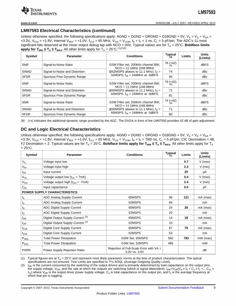
DDC Timing Diagrams
Figure 4. LM97593 Master Reset Timing
Figure 5. LM97593 Synchronization Input (SI) Timing
Figure 6. LM97593 Clock Timing
Figure 7. LM97593 DVGA Interface Timing
Copyright © 2007–2013, Texas Instruments Incorporated Submit Documentation Feedback 11
Product Folder Links: LM97593
SCK_IN
POUT[15:0],
AOUT, BOUT,
RDY and SFS
tDBG
RDY
RDY_POL = 0
new outputold output
RDY
RDY_POL = 1
POUT[15:0]
tPOV
output (n)POUT[15:0]
tSELV
POUT_SEL[2:0]
output (n+1) output (n+2)
n+2n+1n
tOENV tOENT
POUT_EN
POUT[15:0]
LM97593
SNWS019B –JULY 2007–REVISED APRIL 2013 www.ti.com
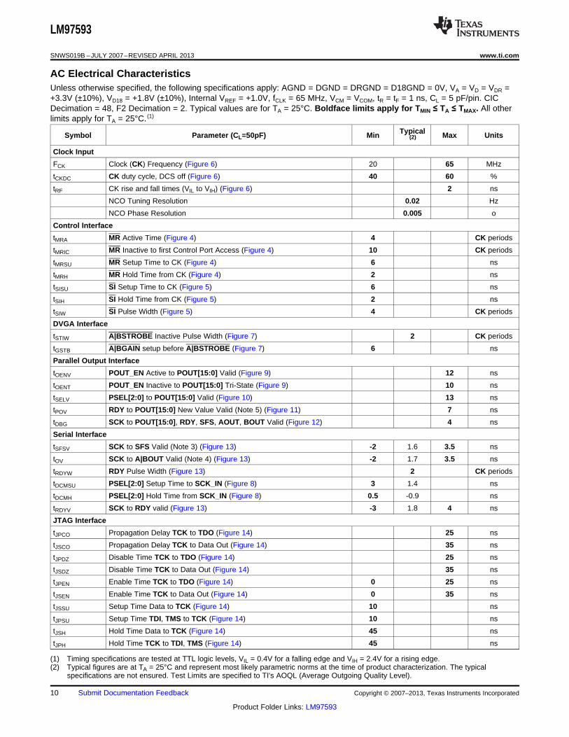
Figure 8. LM97593 Dual Chip Mode Timing
Figure 9. LM97593 Parallel Output Enable Timing
Figure 10. LM97593 Parallel Output Select Timing
Figure 11. LM97593 Parallel Output Data Ready Timing
Figure 12. LM97593 Debug Mode Timing
12 Submit Documentation Feedback Copyright © 2007–2013, Texas Instruments Incorporated
Product Folder Links: LM97593
TCK
TDO
TCK
TDI, TDS
TCK
Data Out
TCK
Data In
tJPDZtJPCO
tJPEN
tJCL
tJPHtJPSU
tJSDZ
tJSSU tJSH
tJSCO
tJSEN
tJCH
LM97593
www.ti.com SNWS019B –JULY 2007–REVISED APRIL 2013
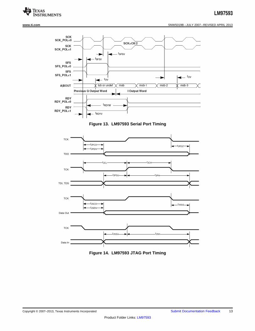
Figure 13. LM97593 Serial Port Timing
Figure 14. LM97593 JTAG Port Timing
Copyright © 2007–2013, Texas Instruments Incorporated Submit Documentation Feedback 13
Product Folder Links: LM97593
LM97593
SNWS019B –JULY 2007–REVISED APRIL 2013 www.ti.com
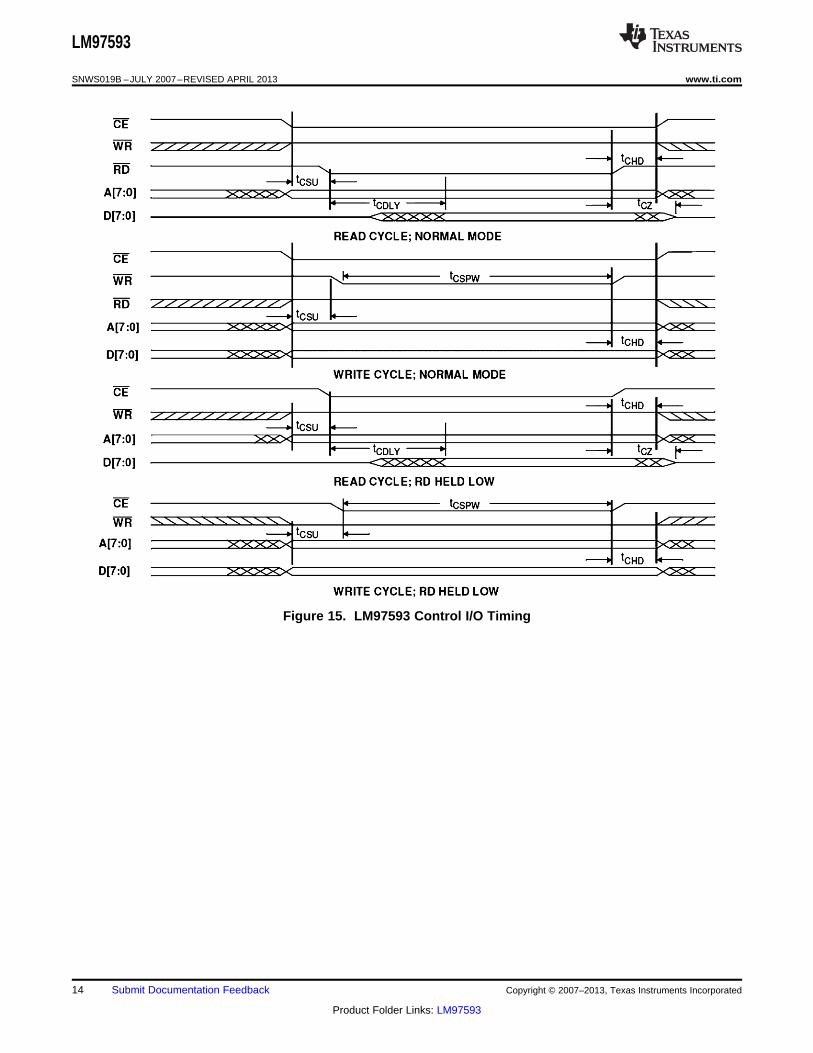
Figure 15. LM97593 Control I/O Timing
14 Submit Documentation Feedback Copyright © 2007–2013, Texas Instruments Incorporated
Product Folder Links: LM97593
LM97593
www.ti.com SNWS019B –JULY 2007–REVISED APRIL 2013
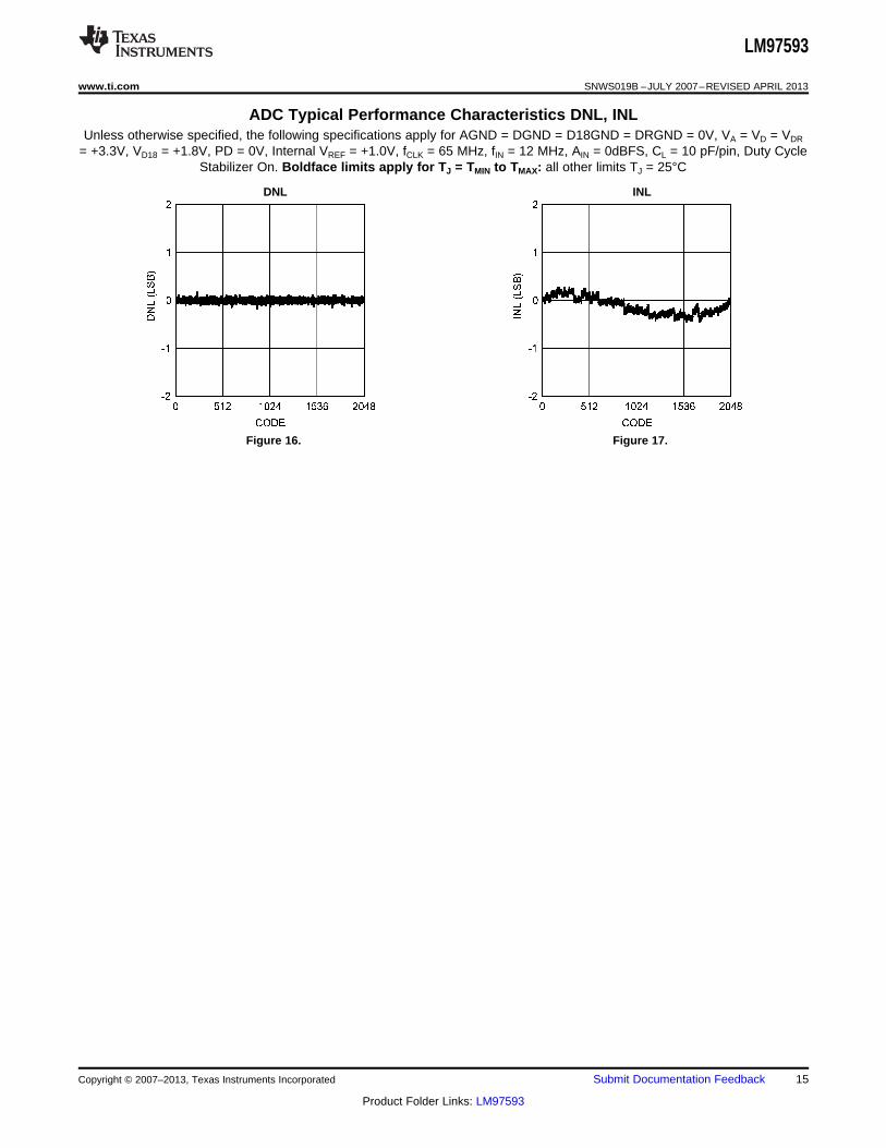
ADC Typical Performance Characteristics DNL, INLUnless otherwise specified, the following specifications apply for AGND = DGND = D18GND = DRGND = 0V, VA = VD = VDR
= +3.3V, VD18 = +1.8V, PD = 0V, Internal VREF = +1.0V, fCLK = 65 MHz, fIN = 12 MHz, AIN = 0dBFS, CL = 10 pF/pin, Duty CycleStabilizer On. Boldface limits apply for TJ = TMIN to TMAX: all other limits TJ = 25°C
DNL INL
Figure 16. Figure 17.
Copyright © 2007–2013, Texas Instruments Incorporated Submit Documentation Feedback 15
Product Folder Links: LM97593
LM97593
SNWS019B –JULY 2007–REVISED APRIL 2013 www.ti.com
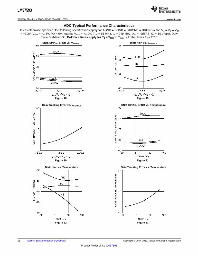
ADC Typical Performance CharacteristicsUnless otherwise specified, the following specifications apply for AGND = DGND = D18GND = DRGND = 0V, VA = VD = VDR
= +3.3V, VD18 = +1.8V, PD = 0V, Internal VREF = +1.0V, fCLK = 65 MHz, fIN = 249 MHz, AIN = -9dBFS, CL = 10 pF/pin, DutyCycle Stabilizer On. Boldface limits apply for TJ = TMIN to TMAX: all other limits TJ = 25°C
SNR, SINAD, SFDR vs. VSUPPLY Distortion vs. VSUPPLY
Figure 18. Figure 19.
Gain Tracking Error vs. VSUPPLY SNR, SINAD, SFDR vs. Temperature
Figure 20. Figure 21.
Distortion vs. Temperature Gain Tracking Error vs. Temperature
Figure 22. Figure 23.
16 Submit Documentation Feedback Copyright © 2007–2013, Texas Instruments Incorporated
Product Folder Links: LM97593
LM97593
www.ti.com SNWS019B –JULY 2007–REVISED APRIL 2013
ADC Typical Performance Characteristics (continued)Unless otherwise specified, the following specifications apply for AGND = DGND = D18GND = DRGND = 0V, VA = VD = VDR
= +3.3V, VD18 = +1.8V, PD = 0V, Internal VREF = +1.0V, fCLK = 65 MHz, fIN = 249 MHz, AIN = -9dBFS, CL = 10 pF/pin, DutyCycle Stabilizer On. Boldface limits apply for TJ = TMIN to TMAX: all other limits TJ = 25°C
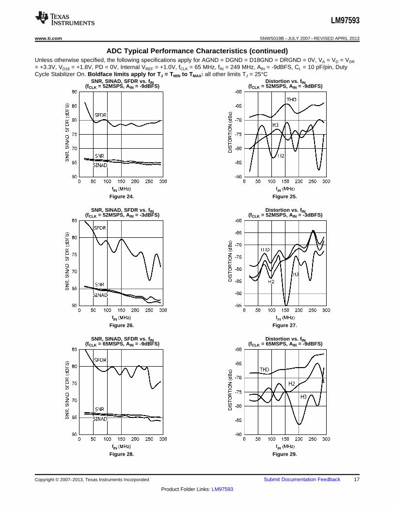
SNR, SINAD, SFDR vs. fIN Distortion vs. fIN(fCLK = 52MSPS, AIN = -9dBFS) (fCLK = 52MSPS, AIN = -9dBFS)
Figure 24. Figure 25.
SNR, SINAD, SFDR vs. fIN Distortion vs. fIN(fCLK = 52MSPS, AIN = -3dBFS) (fCLK = 52MSPS, AIN = -3dBFS)
Figure 26. Figure 27.
SNR, SINAD, SFDR vs. fIN Distortion vs. fIN(fCLK = 65MSPS, AIN = -9dBFS) (fCLK = 65MSPS, AIN = -9dBFS)
Figure 28. Figure 29.
Copyright © 2007–2013, Texas Instruments Incorporated Submit Documentation Feedback 17
Product Folder Links: LM97593
LM97593
SNWS019B –JULY 2007–REVISED APRIL 2013 www.ti.com
ADC Typical Performance Characteristics (continued)Unless otherwise specified, the following specifications apply for AGND = DGND = D18GND = DRGND = 0V, VA = VD = VDR
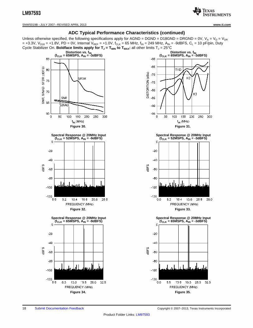
= +3.3V, VD18 = +1.8V, PD = 0V, Internal VREF = +1.0V, fCLK = 65 MHz, fIN = 249 MHz, AIN = -9dBFS, CL = 10 pF/pin, DutyCycle Stabilizer On. Boldface limits apply for TJ = TMIN to TMAX: all other limits TJ = 25°C
Distortion vs. fIN Distortion vs. fIN(fCLK = 65MSPS, AIN = -3dBFS) (fCLK = 65MSPS, AIN = -3dBFS)
Figure 30. Figure 31.
Spectral Response @ 20MHz Input Spectral Response @ 20MHz Input(fCLK = 52MSPS, AIN = -9dBFS) (fCLK = 52MSPS, AIN = -3dBFS)
Figure 32. Figure 33.
Spectral Response @ 20MHz Input Spectral Response @ 20MHz Input(fCLK = 65MSPS, AIN = -9dBFS) (fCLK = 65MSPS, AIN = -3dBFS)
Figure 34. Figure 35.
18 Submit Documentation Feedback Copyright © 2007–2013, Texas Instruments Incorporated
Product Folder Links: LM97593
LM97593
www.ti.com SNWS019B –JULY 2007–REVISED APRIL 2013
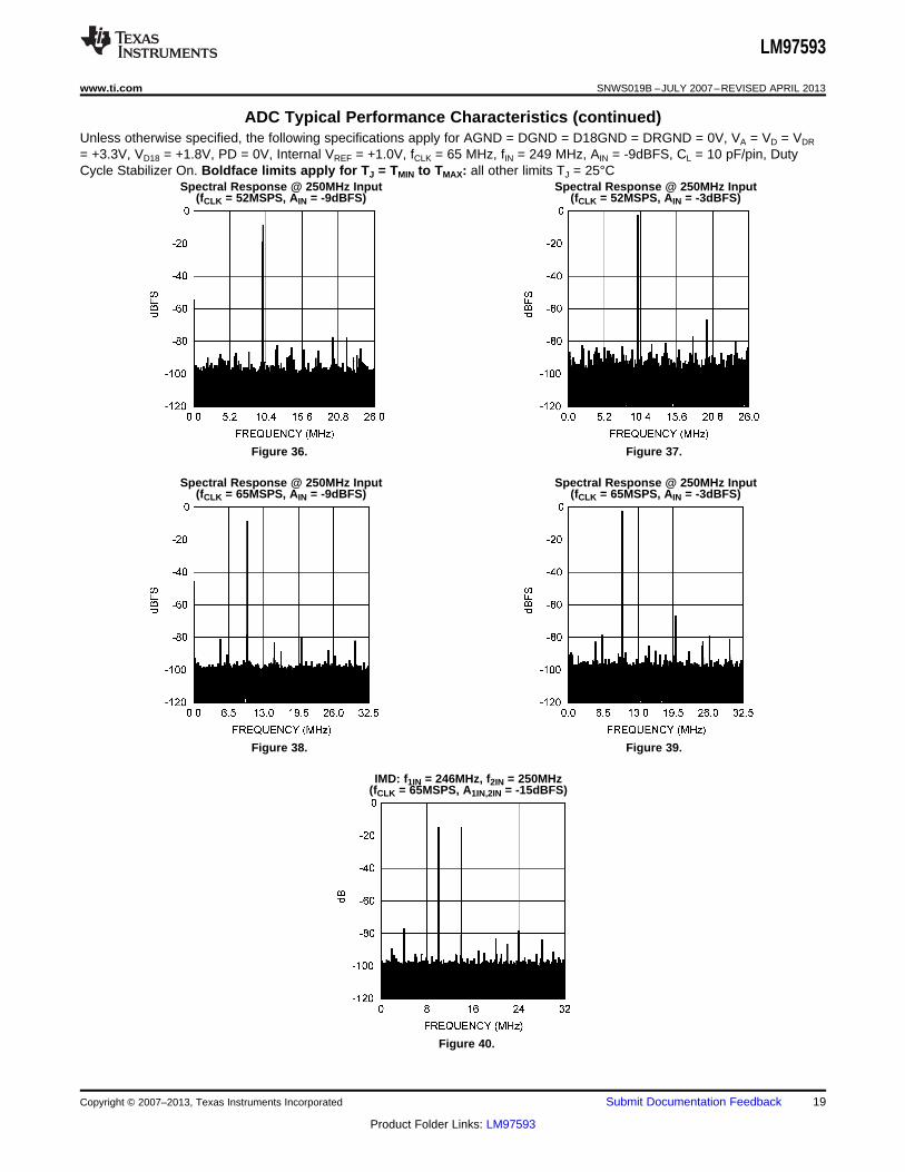
ADC Typical Performance Characteristics (continued)Unless otherwise specified, the following specifications apply for AGND = DGND = D18GND = DRGND = 0V, VA = VD = VDR
= +3.3V, VD18 = +1.8V, PD = 0V, Internal VREF = +1.0V, fCLK = 65 MHz, fIN = 249 MHz, AIN = -9dBFS, CL = 10 pF/pin, DutyCycle Stabilizer On. Boldface limits apply for TJ = TMIN to TMAX: all other limits TJ = 25°C
Spectral Response @ 250MHz Input Spectral Response @ 250MHz Input(fCLK = 52MSPS, AIN = -9dBFS) (fCLK = 52MSPS, AIN = -3dBFS)
Figure 36. Figure 37.
Spectral Response @ 250MHz Input Spectral Response @ 250MHz Input(fCLK = 65MSPS, AIN = -9dBFS) (fCLK = 65MSPS, AIN = -3dBFS)
Figure 38. Figure 39.
IMD: f1IN = 246MHz, f2IN = 250MHz(fCLK = 65MSPS, A1IN,2IN = -15dBFS)
Figure 40.
Copyright © 2007–2013, Texas Instruments Incorporated Submit Documentation Feedback 19
Product Folder Links: LM97593
LM97593
SNWS019B –JULY 2007–REVISED APRIL 2013 www.ti.com
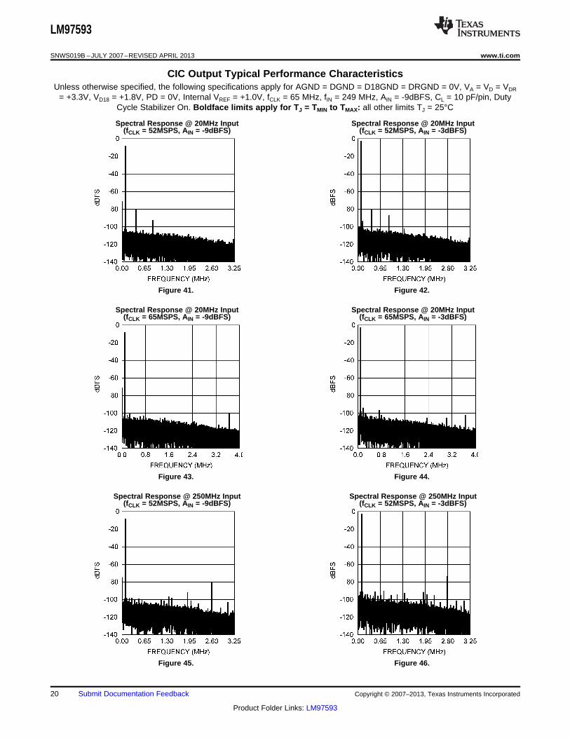
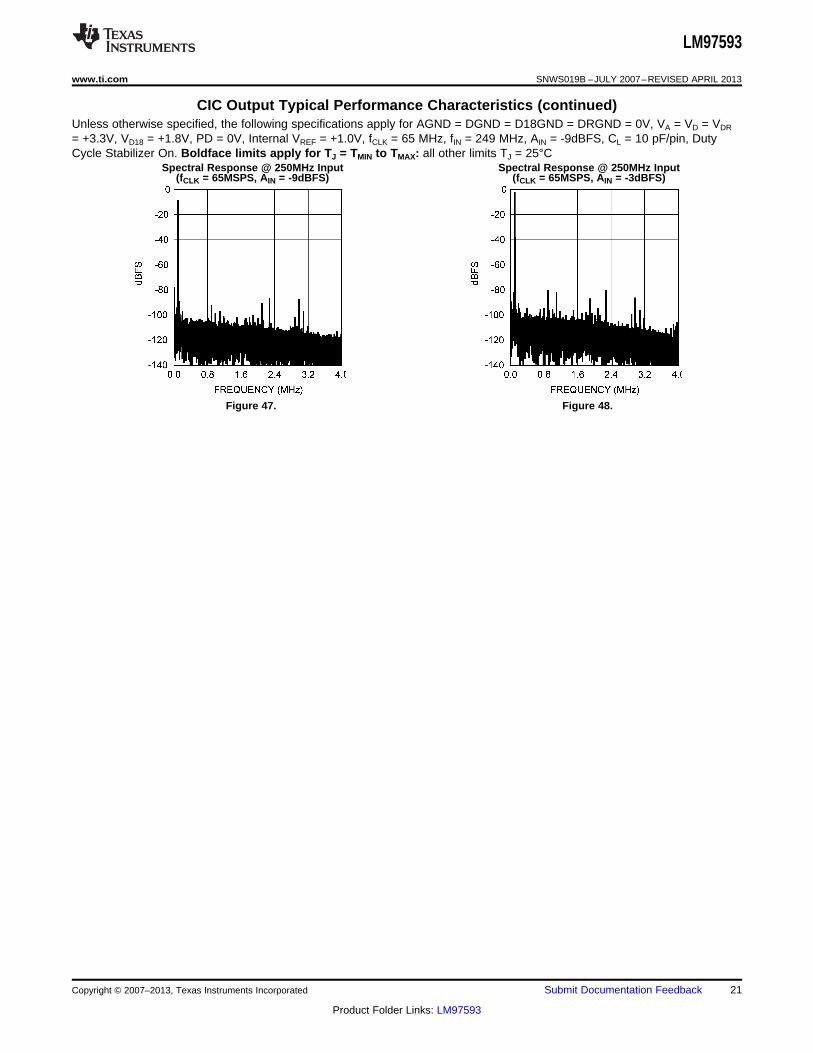
CIC Output Typical Performance CharacteristicsUnless otherwise specified, the following specifications apply for AGND = DGND = D18GND = DRGND = 0V, VA = VD = VDR
= +3.3V, VD18 = +1.8V, PD = 0V, Internal VREF = +1.0V, fCLK = 65 MHz, fIN = 249 MHz, AIN = -9dBFS, CL = 10 pF/pin, DutyCycle Stabilizer On. Boldface limits apply for TJ = TMIN to TMAX: all other limits TJ = 25°C
Spectral Response @ 20MHz Input Spectral Response @ 20MHz Input(fCLK = 52MSPS, AIN = -9dBFS) (fCLK = 52MSPS, AIN = -3dBFS)
Figure 41. Figure 42.
Spectral Response @ 20MHz Input Spectral Response @ 20MHz Input(fCLK = 65MSPS, AIN = -9dBFS) (fCLK = 65MSPS, AIN = -3dBFS)
Figure 43. Figure 44.
Spectral Response @ 250MHz Input Spectral Response @ 250MHz Input(fCLK = 52MSPS, AIN = -9dBFS) (fCLK = 52MSPS, AIN = -3dBFS)
Figure 45. Figure 46.
20 Submit Documentation Feedback Copyright © 2007–2013, Texas Instruments Incorporated
Product Folder Links: LM97593
LM97593
www.ti.com SNWS019B –JULY 2007–REVISED APRIL 2013
CIC Output Typical Performance Characteristics (continued)Unless otherwise specified, the following specifications apply for AGND = DGND = D18GND = DRGND = 0V, VA = VD = VDR
= +3.3V, VD18 = +1.8V, PD = 0V, Internal VREF = +1.0V, fCLK = 65 MHz, fIN = 249 MHz, AIN = -9dBFS, CL = 10 pF/pin, DutyCycle Stabilizer On. Boldface limits apply for TJ = TMIN to TMAX: all other limits TJ = 25°C
Spectral Response @ 250MHz Input Spectral Response @ 250MHz Input(fCLK = 65MSPS, AIN = -9dBFS) (fCLK = 65MSPS, AIN = -3dBFS)
Figure 47. Figure 48.
Copyright © 2007–2013, Texas Instruments Incorporated Submit Documentation Feedback 21
Product Folder Links: LM97593
LM97593
SNWS019B –JULY 2007–REVISED APRIL 2013 www.ti.com
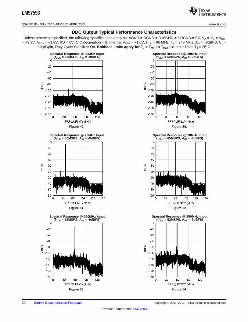
DDC Output Typical Performance CharacteristicsUnless otherwise specified, the following specifications apply for AGND = DGND = D18GND = DRGND = 0V, VA = VD = VDR
= +3.3V, VD18 = +1.8V, PD = 0V, CIC decimation = 8, Internal VREF = +1.0V, fCLK = 65 MHz, fIN = 249 MHz, AIN = -9dBFS, CL =10 pF/pin, Duty Cycle Stabilizer On. Boldface limits apply for TJ = TMIN to TMAX: all other limits TJ = 25°C
Spectral Response @ 20MHz Input Spectral Response @ 20MHz Input(fCLK = 52MSPS, AIN = -9dBFS) (fCLK = 52MSPS, AIN = -3dBFS)
Figure 49. Figure 50.
Spectral Response @ 20MHz Input Spectral Response @ 20MHz Input(fCLK = 65MSPS, AIN = -9dBFS) (fCLK = 65MSPS, AIN = -3dBFS)
Figure 51. Figure 52.
Spectral Response @ 250MHz Input Spectral Response @ 250MHz Input(fCLK = 52MSPS, AIN = -9dBFS) (fCLK = 52MSPS, AIN = -3dBFS)
Figure 53. Figure 54.
22 Submit Documentation Feedback Copyright © 2007–2013, Texas Instruments Incorporated
Product Folder Links: LM97593
LM97593
www.ti.com SNWS019B –JULY 2007–REVISED APRIL 2013
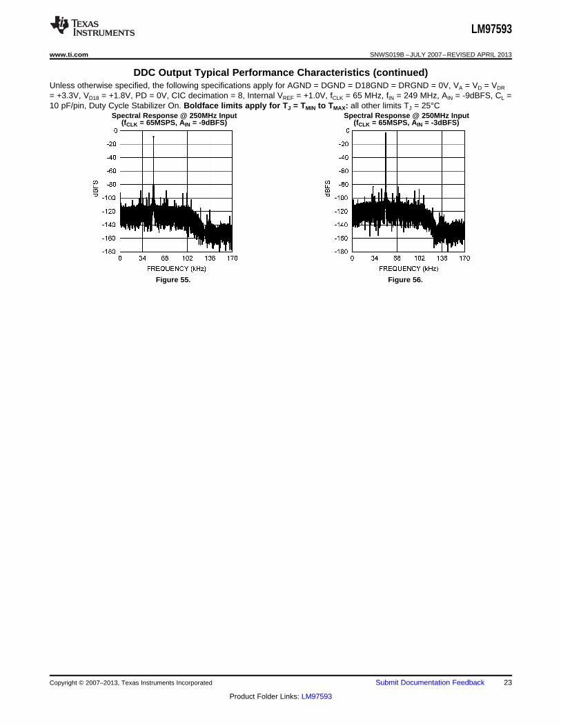
DDC Output Typical Performance Characteristics (continued)Unless otherwise specified, the following specifications apply for AGND = DGND = D18GND = DRGND = 0V, VA = VD = VDR
= +3.3V, VD18 = +1.8V, PD = 0V, CIC decimation = 8, Internal VREF = +1.0V, fCLK = 65 MHz, fIN = 249 MHz, AIN = -9dBFS, CL =10 pF/pin, Duty Cycle Stabilizer On. Boldface limits apply for TJ = TMIN to TMAX: all other limits TJ = 25°C
Spectral Response @ 250MHz Input Spectral Response @ 250MHz Input(fCLK = 65MSPS, AIN = -9dBFS) (fCLK = 65MSPS, AIN = -3dBFS)
Figure 55. Figure 56.
Copyright © 2007–2013, Texas Instruments Incorporated Submit Documentation Feedback 23
Product Folder Links: LM97593
LM97593
SNWS019B –JULY 2007–REVISED APRIL 2013 www.ti.com
FUNCTIONAL DESCRIPTION
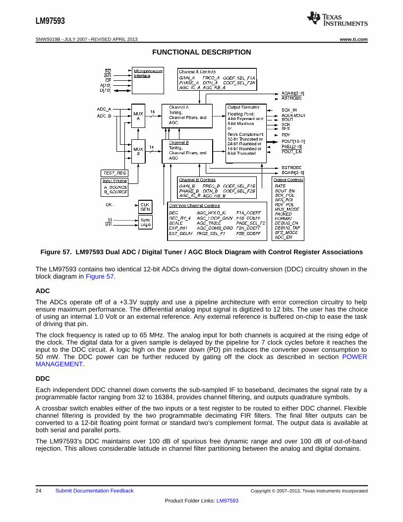
Figure 57. LM97593 Dual ADC / Digital Tuner / AGC Block Diagram with Control Register Associations
The LM97593 contains two identical 12-bit ADCs driving the digital down-conversion (DDC) circuitry shown in theblock diagram in Figure 57.
ADC
The ADCs operate off of a +3.3V supply and use a pipeline architecture with error correction circuitry to helpensure maximum performance. The differential analog input signal is digitized to 12 bits. The user has the choiceof using an internal 1.0 Volt or an external reference. Any external reference is buffered on-chip to ease the taskof driving that pin.
The clock frequency is rated up to 65 MHz. The analog input for both channels is acquired at the rising edge ofthe clock. The digital data for a given sample is delayed by the pipeline for 7 clock cycles before it reaches theinput to the DDC circuit. A logic high on the power down (PD) pin reduces the converter power consumption to50 mW. The DDC power can be further reduced by gating off the clock as described in section POWERMANAGEMENT.
DDC
Each independent DDC channel down converts the sub-sampled IF to baseband, decimates the signal rate by aprogrammable factor ranging from 32 to 16384, provides channel filtering, and outputs quadrature symbols.
A crossbar switch enables either of the two inputs or a test register to be routed to either DDC channel. Flexiblechannel filtering is provided by the two programmable decimating FIR filters. The final filter outputs can beconverted to a 12-bit floating point format or standard two’s complement format. The output data is available atboth serial and parallel ports.
The LM97593’s DDC maintains over 100 dB of spurious free dynamic range and over 100 dB of out-of-bandrejection. This allows considerable latitude in channel filter partitioning between the analog and digital domains.
24 Submit Documentation Feedback Copyright © 2007–2013, Texas Instruments Incorporated
Product Folder Links: LM97593
LM97593
www.ti.com SNWS019B –JULY 2007–REVISED APRIL 2013
The frequencies, phase offsets, and phase dither of the two sine/cosine numerically controlled oscillators (NCOs)can be independently specified. Two sets of coefficient memories and a crossbar switch allow shared orindependent filter coefficients and bandwidth for each channel. Both channels share the same decimation ratioand input/output formats.
Each channel has its own AGC circuit for use with narrowband radio channels where most of the channel filteringprecedes the ADC. The AGC closes the loop around the DVGA, compressing the dynamic range of the signalinto the ADC. AGC gain compensation in the LM97593 removes the DVGA gain steps at the output. The timealignment of this gain compensation circuit can be adjusted. The AGC can be configured to operate continuouslyor set to a fixed gain. The two AGC circuits operate independently but share the same programmed parametersand control signals.
The chip receives configuration and control information over a microprocessor-compatible bus consisting of an 8-bit data I/O port, an 8-bit address port, a chip enable strobe, a read strobe, and a write strobe. The chip’s controlregisters (8 bits each) are memory mapped into the 8-bit address space of the control port. Page select bits allowaccess to the overlaid A and B set of FIR coefficients.
JTAG boundary scan and on-chip diagnostic circuits are provided to simplify system debug and test.
The LM97593 supports 3.3V I/O even though the core logic voltage is 1.8V. The LM97593 outputs swing to the3.3V rail so they can be directly connected to 5V TTL inputs if desired.
ADC Application Information
ADC OPERATING CONDITIONS
We recommend that the following conditions be observed for operation:3.0V ≤ VA ≤ 3.6VVD = VA = VDR
VD18 = 1.8V10 MHz ≤ fCLK ≤ 65 MHz1.0 V internal referenceVCM = 1.5V (from VCOMA and VCOMB)
Analog Inputs
There is one reference input pin, VREF, which is used to select an internal reference, or to supply an externalreference. The ADC has two analog signal input pairs, VIN A+ and VIN A- for one converter and VIN B+ and VIN B-for the other converter. Each pair of pins forms a differential input pair.
Reference Pins
The ADC is designed to operate with an internal 1.0V reference or an external 1.0V reference, but performs wellwith external reference voltages in the range of 0.8V to 1.2V. Lower reference voltages will decrease the signal-to-noise ratio (SNR) of the ADC. Increasing the reference voltage (and the input signal swing) beyond 1.2V maydegrade THD for a full-scale input, especially at higher input frequencies.
It is important that all grounds associated with the reference voltage and the analog input signal make connectionto the ground plane at a single, quiet point to minimize the effects of noise currents in the ground path.
The six Reference Bypass Pins (VRPA, VCOMA, VRNA, VRPB, VCOMB and VRNB) are made available for bypasspurposes. All these pins should each be bypassed to ground with a 0.1 µF capacitor. A 10 µF capacitor shouldbe placed between the VRPA and VRNA pins and between the VRPB and VRNB pins, as shown in Figure 86. Thisconfiguration is necessary to avoid reference oscillation, which could result in reduced SFDR and/or SNR.
Smaller capacitor values than those specified will allow faster recovery from the power down mode, but mayresult in degraded noise performance. Loading any of these pins other than VCOMA and VCOMB may result inperformance degradation.
Copyright © 2007–2013, Texas Instruments Incorporated Submit Documentation Feedback 25
Product Folder Links: LM97593
LM97593
SNWS019B –JULY 2007–REVISED APRIL 2013 www.ti.com
The nominal voltages for the reference bypass pins are as follows:
VCOM = 1.5 V
VRP = VCOM + VREF / 2
VRN = VCOM − VREF / 2
User choice of an on-chip or external reference voltage is provided. The internal 1.0 Volt reference is in usewhen the the VREF pin is connected to VA. If a voltage in the range of 0.8V to 1.2V is applied to the VREF pin, thatis used for the voltage reference. When an external reference is used, the VREF pin should be bypassed toground with a 0.1 µF capacitor close to the reference input pin. There is no need to bypass the VREF pin whenthe internal reference is used.
Signal Inputs
The signal inputs are VIN A+ and VINA− for one ADC and VINB+ and VINB− for the other ADC . The input signal,VIN, is defined as
VIN A = (VINA+) – (VINA−) (1)
for the "A" converter and
VIN B = (VINB+) – (VINB−) (2)
for the "B" converter.
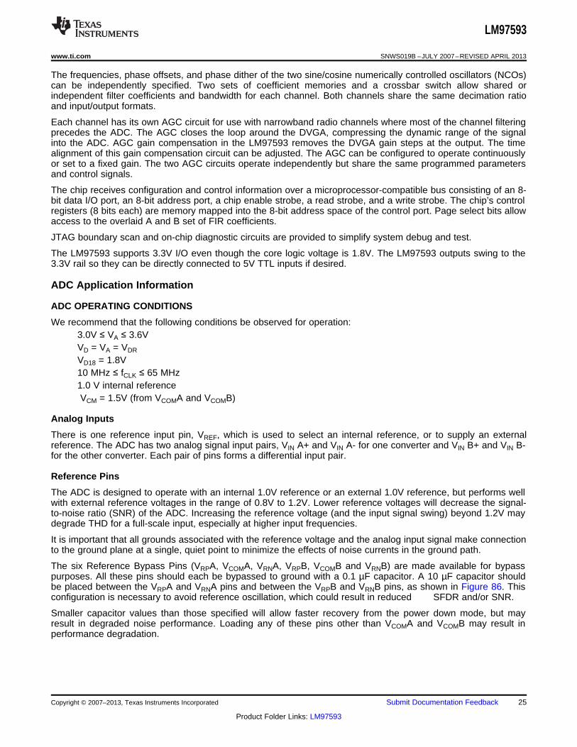
Figure 58 shows the expected input signal range. Note that the common mode input voltage, VCM, should be inthe range of 1.0V to 2.0V.
The peaks of the individual input signals should never exceed 2.6V.
The ADC performs best with a differential input signal with each input centered around a common mode voltage,VCM. The peak-to-peak voltage swing at each analog input pin should not exceed the value of the referencevoltage or the output data will be clipped.
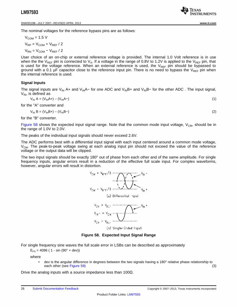
The two input signals should be exactly 180° out of phase from each other and of the same amplitude. For singlefrequency inputs, angular errors result in a reduction of the effective full scale input. For complex waveforms,however, angular errors will result in distortion.
Figure 58. Expected Input Signal Range
For single frequency sine waves the full scale error in LSBs can be described as approximatelyEFS = 4096 ( 1 - sin (90° + dev))
where• dev is the angular difference in degrees between the two signals having a 180° relative phase relationship to
each other (see Figure 59) (3)
Drive the analog inputs with a source impedance less than 100Ω.
26 Submit Documentation Feedback Copyright © 2007–2013, Texas Instruments Incorporated
Product Folder Links: LM97593
LM97593
www.ti.com SNWS019B –JULY 2007–REVISED APRIL 2013
Figure 59. Angular Errors Between the Two Input Signals Will Reduce the Output Level or CauseDistortion
For differential operation, each analog input pin of the differential pair should have a peak-to-peak voltage equalto the reference voltage, VREF, be 180 degrees out of phase with each other and be centered around VCM.
Single-Ended Operation
Performance with differential input signals is better than with single-ended signals. For this reason, single-endedoperation is not recommended. However, if single ended-operation is required and the resulting performancedegradation is acceptable, one of the analog inputs should be connected to the d.c. mid point voltage of thedriven input. The peak-to-peak input signal at the driven input pin should be twice the reference voltage tomaximize SNR and SINAD performance (Figure 58b). For example, set VREF to 1.0V, bias VIN− to 1.5V and driveVIN+ with a signal range of 0.5V to 2.5V.
Because very large input signal swings can degrade distortion performance, better performance with a single-ended input can be obtained by reducing the reference voltage when maintaining a full-range output.
Driving the Analog Inputs
The VIN+ and the VIN− inputs of the ADC consist of an analog switch followed by a switched-capacitor amplifier.As the internal sampling switch opens and closes, current pulses occur at the analog input pins, resulting involtage spikes at the signal input pins. As the driving source attempts to counteract these voltage spikes, it mayadd noise to the signal at the ADC analog input. C1, C2, and C3 as shown in Figure 86 improve the ADCperformance by filtering these voltage spikes. These components should be placed close to the ADC inputsbecause the input pins of the ADC are the most sensitive part of the system and this is the last opportunity tofilter that input.
For Nyquist applications the RC pole should be at the ADC sample rate. The ADC input capacitance in thesample mode should be considered when setting the RC pole. For wideband undersampling applications, the RCpole should be set at about 1.5 to 2 times the maximum input frequency to maintain a linear delay response. Thevalues of the RC shown in Figure 86 are suitable for applications with input frequencies up to approximately70MHz.
Input Common Mode Voltage
The input common mode voltage, VCM, should be in the range of 1.0V to 2.0V and be a value such that the peakexcursions of the analog signal do not go more negative than ground or more positive than 2.6V. See ReferencePins.
DIGITAL INPUTS
Digital TTL/CMOS compatible inputs consist of CK, REFSEL/DCS.
CLK
The CLK signal controls the timing of the sampling process. Drive the clock input with a stable, low jitter clocksignal in the range of 10 MHz to 65 MHz. The higher the input frequency, the more critical it is to have a low jitterclock. The trace carrying the clock signal should be as short as possible and should not cross any other signalline, analog or digital, not even at 90°.
The CLK signal also drives an internal state machine. If the CLK is interrupted, or its frequency too low, thecharge on internal capacitors can dissipate to the point where the accuracy of the output data will degrade. Thisis what limits the lowest sample rate.
Copyright © 2007–2013, Texas Instruments Incorporated Submit Documentation Feedback 27
Product Folder Links: LM97593
LM97593
SNWS019B –JULY 2007–REVISED APRIL 2013 www.ti.com
The clock line should be terminated at its source in the characteristic impedance of that line. Take care tomaintain a constant clock line impedance throughout the length of the line. Refer to Application Note AN-905(literature number SNLA035) for information on setting characteristic impedance.
It is highly desirable that the the source driving the ADC CLK pin only drive that pin. However, if that source isused to drive other things, each driven pin should be a.c. terminated with a series RC to ground such that theresistor value is equal to the characteristic impedance of the clock line and the capacitor value is
where• tPD is the signal propagation time down the clock line• "L" is the line length• ZO is the characteristic impedance of the clock line (4)
This termination should be as close as possible to the ADC clock pin but beyond it as seen from the clocksource. Typical tPD is about 150 ps/inch (60 ps/cm) on FR-4 board material. The units of "L" and tPD should bethe same (inches or centimeters).
The duty cycle of the clock signal can affect the performance of the A/D Converter. Because achieving a preciseduty cycle is difficult, the LM97593 has a Duty Cycle Stabilizer which can be enabled using the REFSEL/DCSpin. It is designed to maintain performance over a clock duty cycle range of 30% to 70% at 65 MSPS.
REFSEL/DCS
This pin is used in conjunction with VREF (pin 21) to select the reference source and turn the Duty CycleStabilizer (DCS) on or off.
When REFSEL/DCS is LOW and VREF is HIGH, the internal 1.0V reference is selected and DCS is On.
When REFSEL/DCS is HIGH, an external reference voltage in the range of 0.8V to 1.2V should be applied to theVREF input. DCS is On.
With REFSEL/DCS pin connected to VCOMA or VCOMB, the internal 1.0V reference is selected and DCS is Off.
When enabled, duty cycle stabilization can compensate for clock inputs with duty cycles ranging from 30% to70% and generate a stable internal clock, improving the performance of the part.
Table 1. VREF, REFSEL/DCS Pin Functions
REFSEL/DCS (pin 8) VREF (pin 21) Reference DCS
Logic Low Logic High Internal 1.0 V ON
Logic High 0.8 to 1.2V External ON
VCOMA or VCOMB Logic High Internal 1.0V OFF
VCOMA or VCOMB 0.8 to 1.2V External OFF
PD
The PD pin, when high, holds the ADC in a power-down mode to conserve power when the converter is notbeing used. The output data pins are undefined and the data in the pipeline is corrupted while in the power downmode.
The Power Down Mode Exit Cycle time is determined by the value of the components on pins 15, 16, 17, 22, 23and 24. These capacitors lose their charge in the Power Down mode and must be recharged by on-chip circuitrybefore conversions can be accurate. Smaller capacitor values allow slightly faster recovery from the power downmode, but can result in a reduction in SNR, SINAD and ENOB performance.
28 Submit Documentation Feedback Copyright © 2007–2013, Texas Instruments Incorporated
Product Folder Links: LM97593
LM97593
www.ti.com SNWS019B –JULY 2007–REVISED APRIL 2013
DDC Application Information
CONTROL INTERFACE
The LM97593 is configured by writing control information into 237 control registers within the chip. The contentsof these control registers and how to use them are described in Control Register Addresses and Defaults. Theregisters are written to or read from using the D[7:0], A[7:0], CE, RD and WR pins. This interface is designed toallow the LM97593 to appear to an external processor as a memory mapped peripheral. See Figure 15 fordetails.
The control interface is asynchronous with respect to the system clock, CK. This allows the registers to bewritten or read at any time. In some cases this might cause an invalid operation since the interface is notinternally synchronized. In order to assure correct operation, SI must be asserted after the control registers arewritten.
The D[7:0], A[7:0], WR, RD and CE pins should not be driven above the positive supply voltage.
Master Reset
A master reset pin, MR, is provided to initialize the LM97593 to a known condition and should be strobed afterpower up. This signal will clear all sample data and all user programmed data (filter coefficients and AGCsettings). All outputs will be disabled (tri-stated). ASTROBE and BSTROBE will be asserted to initialize theDVGA values. Control Register Addresses and Defaults describes the control register default values.
Synchronizing Multiple LM97593 Chips
A system containing two or more LM97593 chips will need to be synchronized if coherent operation is desired.To synchronize multiple LM97593 chips, connect all of the sync input pins together so they can be driven by acommon sync strobe. Synchronization occurs on the first rising edge of CK after SI goes high. When SI isasserted all sample data is immediately cleared, the numerically controlled oscillator (NCO) phase offset isinitialized, the NCO dither generators are reset, and the CIC decimation ratio is initialized. Only the configurationdata loaded into the microprocessor interface remains unaffected.
SI may be held low as long as desired after a minimum of 4 CK periods.
Input Source
The input crossbar switch allows either VINA, VINB, or a test register to be routed to the channel A or channel BAGC/ DDC. The AGC outputs, AGAIN and BGAIN, are not switched. If VINA and VINB are exchanged the AGCloop will be open and the AGC will not function properly.
Selecting the test register as the input source allows the AGC or DDC operation to be verified with a knowninput. See Test Register for further discussion.
DOWN CONVERTERS
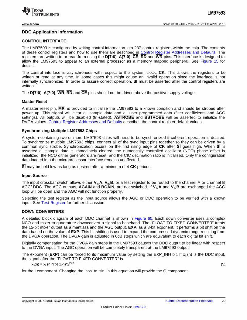
A detailed block diagram of each DDC channel is shown in Figure 60. Each down converter uses a complexNCO and mixer to quadrature downconvert a signal to baseband. The “FLOAT TO FIXED CONVERTER” treatsthe 15-bit mixer output as a mantissa and the AGC output, EXP, as a 3-bit exponent. It performs a bit shift on thedata based on the value of EXP. This bit shifting is used to expand the compressed dynamic range resulting fromthe DVGA operation. The DVGA gain is adjusted in 6dB steps which are equivalent to each digital bit shift.
Digitally compensating for the DVGA gain steps in the LM97593 causes the DDC output to be linear with respectto the DVGA input. The AGC operation will be completely transparent at the LM97593 output.
The exponent (EXP) can be forced to its maximum value by setting the EXP_INH bit. If xin(n) is the DDC input,the signal after the “FLOAT TO FIXED CONVERTER” is
x3(n) = xin(n)*cos(ωn)*2EXP (5)
for the I component. Changing the ‘cos’ to ‘sin’ in this equation will provide the Q component.
Copyright © 2007–2013, Texas Instruments Incorporated Submit Documentation Feedback 29
Product Folder Links: LM97593
SH
IFT
UP
SH
IFT
UP
CIC
FIL
TE
R
DE
CIM
AT
ION
BY
8 T
O 2
k
SA
T &
RO
UN
D
SA
T &
RO
UN
D
SA
T
TO
OUTPUT
CIRCUITRO
UN
D
FLO
AT
TO
FIX
ED
CO
NV
ER
TE
R
N = DEC + 1
Data @ FCK/N
SC
ALE
DE
C
GA
IN_
A
F1
_C
OE
F
F2
_C
OE
F
DE
C_
BY
_4
Data @ FCK/N*2 Data @ FCK/N*2*F2_DEC= OFS (Output FSAMPLE)
Data @ FCK
= FS (FSAMPLE)
PHASE_A
FREQ_A
MUXA
EXP(from AGC)
EX
P_I
NH
EXP
NCO
F2
FIL
TE
R
DE
CIM
AT
E B
Y
2 O
R 4
F1
FIL
TE
R
DE
CIM
AT
E B
Y 2
COSSIN
17 17
15 22 21 21
15
3
14
22 21 21
EXPONENT
Q
I
LM97593
SNWS019B –JULY 2007–REVISED APRIL 2013 www.ti.com
The “FLOAT TO FIXED CONVERTER” circuit expands the dynamic range compression performed by the DVGA.Signals from this point onward extend across the full dynamic range of the signals applied to the DVGA input.This allows the AGC to operate continuously through a burst without producing artifacts in the signal due to thesettling response of the decimation filters after a 6dB DVGA gain adjustment. For example, if the DVGA inputsignal were to increase causing the ADC output level to cross the AGC threshold level, the gain of the DVGAwould change by -6dB. The 6dB step is allowed to propagate through the ADC and mixers and is compensatedout just before the filtering. The accuracy of the compensation is dependent on timing and the accuracy of theDVGA gain step. The LM97593 allows the timing of the gain compensation to be adjusted in the EXT_DELAYregister; see the end of section AGC for more information. The AGC requires 21 bits (14-bit internal bus output +7-bit shift) to represent the full linear dynamic range of the signal. The output word must be set to either 24-bit or32-bit to take advantage of the entire dynamic range available. The LM97593 can also be configured to output afloating point format with up to 138dB of numerical resolution using only 12 output bits.
Figure 60. LM97593 Down Converter, Channel A (Channel B is identical)
The “SHIFT UP” circuit will be discussed in the section Four Stage CIC Filter.
A 4-stage cascaded-integrator-comb (CIC) filter and a two-stage decimate by 4 or 8 finite impulse response (FIR)filter are used to lowpass filter and isolate the desired signal. The CIC filter reduces the sample rate by aprogrammable factor ranging from 8 to 2048 (decimation ratio). The CIC outputs are followed by a gain stageand then followed by a two-stage decimate by 4 or 8 filter. The gain circuit allows the user to boost the gain ofweak signals by up to 42 dB in 6 dB steps. It also rounds the signal to 21 bits and saturates at plus or minus fullscale.
The first stage of the two stage filter is a 21-tap, symmetric decimate by 2 FIR filter (F1) with programmable 16bit tap weights. The coefficients of the first 11 taps are downloaded to the chip as 16 bit words. Since the filter isa symmetric configuration only the first 11 coefficients must be loaded. First Programmable FIR Filter (F1)provides a generic set of coefficients that compensate for the rolloff of the CIC filter and provide a passband flatto 0.01dB with 70 dB of out of band rejection. A second coefficient set is provided that has a narrower outputpassband and greater out-of-band rejection. The second set of coefficients is ideal for systems such as GSMwhere far-image rejection is more important than adjacent channel rejection.
The second stage is a 63 tap decimate by 2 or 4 programmable FIR filter (F2) also with 16 bit tap weights. Filtercoefficients for a flat response from -0.4FS to +0.4FS of the output sample rate with 80dB of out of band rejectionare provided in Second Programmable FIR Filter (F2). A second set of F2 coefficients is also provided toenhance performance for GSM systems. The user can also design and download their own final filter tocustomize the channel’s spectral response. Typical uses of programmable filter F2 include matched (root-raisedcosine) filtering, or filtering to generate oversampled outputs with greater out of band rejection. The 63 tapsymmetrical filter is downloaded into the chip as 32 words, 16 bits each. Saturation to plus or minus full scale isperformed at the output of F1 and F2 to clip the signal rather than allow it to roll over.
30 Submit Documentation Feedback Copyright © 2007–2013, Texas Instruments Incorporated
Product Folder Links: LM97593
LM97593
www.ti.com SNWS019B –JULY 2007–REVISED APRIL 2013
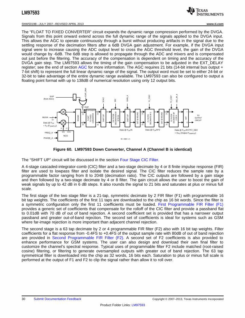
Figure 61. Complex NCO Output Phase Dither DisabledExample of NCO spurs due to phase truncation
(Before Phase Dithering)
The LM97593 provides two sets of coefficient memory for both F1 and F2. These coefficient memories can beindependently routed to channel A, channel B, or both channel A and B with a crossbar switch. The coefficientscan be switched on the fly but some time will be required before valid output data is available.
The Numerically Controlled Oscillator
The tuning frequency of each down converter is specified as a 32 bit word (.02Hz resolution at CK=52MHz) andthe phase offset is specified as a 16 bit word (.005o). These two parameters are applied to the NumericallyControlled Oscillator (NCO) circuit to generate sine and cosine signals used by the digital mixer. The NCOs canbe synchronized with NCOs on other chips via the sync pin SI. This allows multiple down converter outputs to becoherently combined, each with a unique phase and amplitude.
The tuning frequency is set by loading the FREQ register according to the formula FREQ = 232F/FCK, where F isthe desired tuning frequency and FCK is the chip’s clock rate. FREQ is a 2’s complement word. The range for F isfrom -FCK/2 to +FCK(1-2-31)/2.
If a sub-sampled signal is in an even Nyquist zone the sampling process causes the order of the I and Qcomponents to be reversed. Should this occur simply invert the polarity of the tuning frequency F.
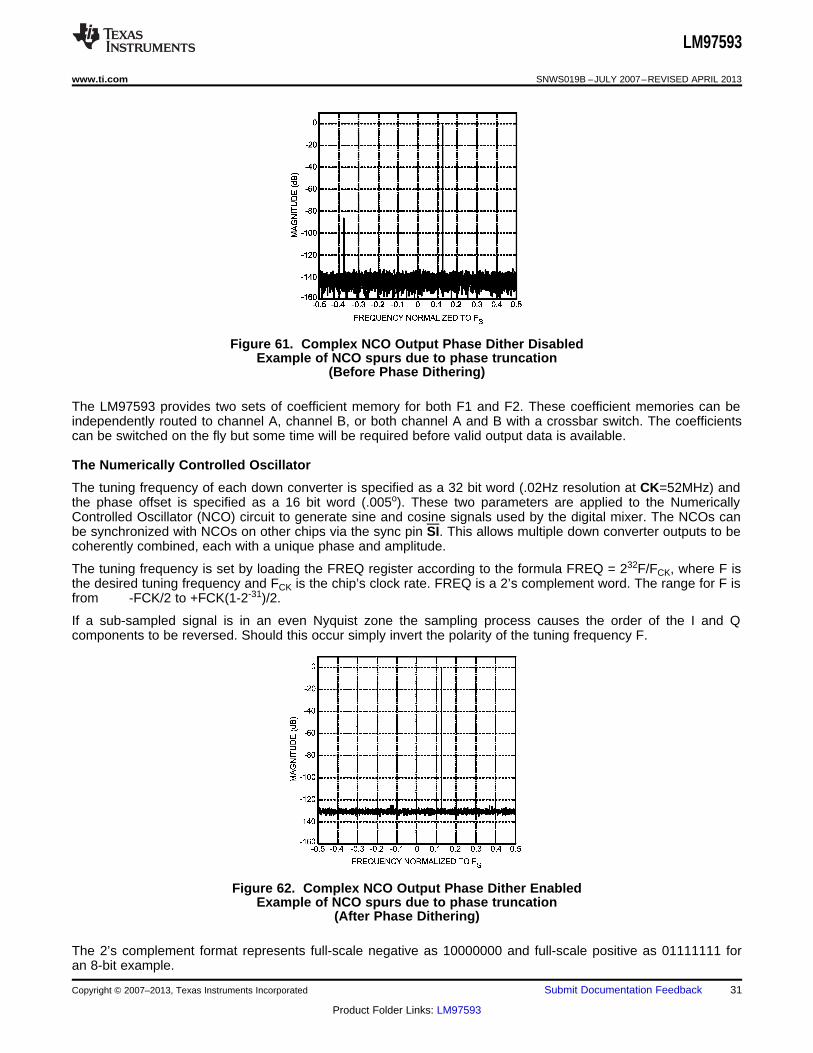
Figure 62. Complex NCO Output Phase Dither EnabledExample of NCO spurs due to phase truncation
(After Phase Dithering)
The 2’s complement format represents full-scale negative as 10000000 and full-scale positive as 01111111 foran 8-bit example.
Copyright © 2007–2013, Texas Instruments Incorporated Submit Documentation Feedback 31
Product Folder Links: LM97593
LM97593
SNWS019B –JULY 2007–REVISED APRIL 2013 www.ti.com
The 16 bit phase offset is set by loading the PHASE register according to the formula PHASE = 216P/2π, whereP is the desired phase in radians ranging between 0 and 2π. PHASE is an unsigned 16-bit number. P rangesfrom 0 to 2π(1-2-16). Phase dithering can be enabled to reduce the spurious signals created by the NCO due tophase truncation. This truncation is unavoidable since the frequency resolution is much finer than the phaseresolution. With dither enabled, spurs due to phase truncation are below -100 dBc for all frequencies and phaseoffsets. Each NCO has its own dither source and the initial state of one is maximally offset with respect to theother so that they are effectively uncorrelated. The phase dither sources are on by default. They areindependently controlled by the DITH_A and DITH_B bits. The amplitude resolution of the ROM creates a worst-case spur amplitude of -101dBc rendering amplitude dither unnecessary.
The spectrum plots in Figure 61 and Figure 62show the effectiveness of phase dither in reducing NCO spurs dueto phase truncation for a worst-case example (just below FS/8). With dither off, the spur is at -86.4dBFS. Withdither on, the spur is below -125dBFS, disappearing into the noise floor. This spur is spread into the noise floorwhich results in an SNR of -83.6dBFS. The channel filter’s processing gain will further improve the SNR.
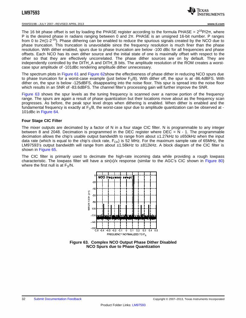
Figure 63 shows the spur levels as the tuning frequency is scanned over a narrow portion of the frequencyrange. The spurs are again a result of phase quantization but their locations move about as the frequency scanprogresses. As before, the peak spur level drops when dithering is enabled. When dither is enabled and thefundamental frequency is exactly at FS/8, the worst-case spur due to amplitude quantization can be observed at -101dBc in Figure 64.
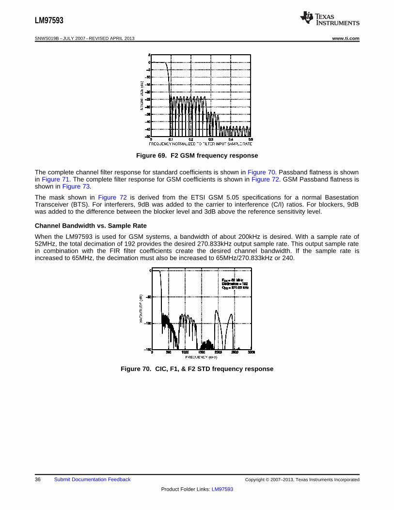
Four Stage CIC Filter
The mixer outputs are decimated by a factor of N in a four stage CIC filter. N is programmable to any integerbetween 8 and 2048. Decimation is programmed in the DEC register where DEC = N - 1. The programmabledecimation allows the chip’s usable output bandwidth to range from about ±1.27kHz to ±650kHz when the inputdata rate (which is equal to the chip’s clock rate, FCK) is 52 MHz. For the maximum sample rate of 65MHz, theLM97593’s output bandwidth will range from about ±1.58kHz to ±812kHz. A block diagram of the CIC filter isshown in Figure 65.
The CIC filter is primarily used to decimate the high-rate incoming data while providing a rough lowpasscharacteristic. The lowpass filter will have a sin(x)/x response (similar to the AGC’s CIC shown in Figure 80)where the first null is at FS/N.
Figure 63. Complex NCO Output Phase Dither DisabledNCO Spurs due to Phase Quantization
32 Submit Documentation Feedback Copyright © 2007–2013, Texas Instruments Incorporated
Product Folder Links: LM97593
LM97593
www.ti.com SNWS019B –JULY 2007–REVISED APRIL 2013
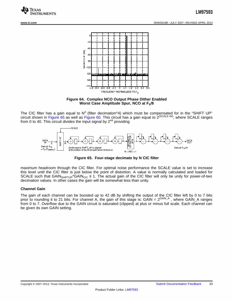
Figure 64. Complex NCO Output Phase Dither EnabledWorst Case Amplitude Spur, NCO at FS/8
The CIC filter has a gain equal to N4 (filter decimation^4) which must be compensated for in the “SHIFT UP”circuit shown in Figure 65 as well as Figure 60. This circuit has a gain equal to 2(SCALE-44), where SCALE rangesfrom 0 to 40. This circuit divides the input signal by 244 providing
Figure 65. Four-stage decimate by N CIC filter
maximum headroom through the CIC filter. For optimal noise performance the SCALE value is set to increasethis level until the CIC filter is just below the point of distortion. A value is normally calculated and loaded forSCALE such that GAINSHIFTUP*GAINCIC ≤ 1. The actual gain of the CIC filter will only be unity for power-of-twodecimation values. In other cases the gain will be somewhat less than unity.
Channel Gain
The gain of each channel can be boosted up to 42 dB by shifting the output of the CIC filter left by 0 to 7 bitsprior to rounding it to 21 bits. For channel A, the gain of this stage is: GAIN = 2GAIN_A , where GAIN_A rangesfrom 0 to 7. Overflow due to the GAIN circuit is saturated (clipped) at plus or minus full scale. Each channel canbe given its own GAIN setting.
Copyright © 2007–2013, Texas Instruments Incorporated Submit Documentation Feedback 33
Product Folder Links: LM97593
LM97593
SNWS019B –JULY 2007–REVISED APRIL 2013 www.ti.com
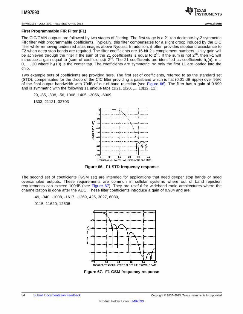
First Programmable FIR Filter (F1)
The CIC/GAIN outputs are followed by two stages of filtering. The first stage is a 21 tap decimate-by-2 symmetricFIR filter with programmable coefficients. Typically, this filter compensates for a slight droop induced by the CICfilter while removing undesired alias images above Nyquist. In addition, it often provides stopband assistance toF2 when deep stop bands are required. The filter coefficients are 16-bit 2’s complement numbers. Unity gain willbe achieved through the filter if the sum of the 21 coefficients is equal to 216. If the sum is not 216, then F1 willintroduce a gain equal to (sum of coefficients)/ 216. The 21 coefficients are identified as coefficients h1(n), n =0, ..., 20 where h1(10) is the center tap. The coefficients are symmetric, so only the first 11 are loaded into thechip.
Two example sets of coefficients are provided here. The first set of coefficients, referred to as the standard set(STD), compensates for the droop of the CIC filter providing a passband which is flat (0.01 dB ripple) over 95%of the final output bandwidth with 70dB of out-of-band rejection (see Figure 66). The filter has a gain of 0.999and is symmetric with the following 11 unique taps (1|21, 2|20, ..., 10|12, 11):
29, -85, -308, -56, 1068, 1405, -2056, -6009,
1303, 21121, 32703
Figure 66. F1 STD frequency response
The second set of coefficients (GSM set) are intended for applications that need deeper stop bands or needoversampled outputs. These requirements are common in cellular systems where out of band rejectionrequirements can exceed 100dB (see Figure 67). They are useful for wideband radio architectures where thechannelization is done after the ADC. These filter coefficients introduce a gain of 0.984 and are:
-49, -340, -1008, -1617, -1269, 425, 3027, 6030,
9115, 11620, 12606
Figure 67. F1 GSM frequency response
34 Submit Documentation Feedback Copyright © 2007–2013, Texas Instruments Incorporated
Product Folder Links: LM97593
LM97593
www.ti.com SNWS019B –JULY 2007–REVISED APRIL 2013
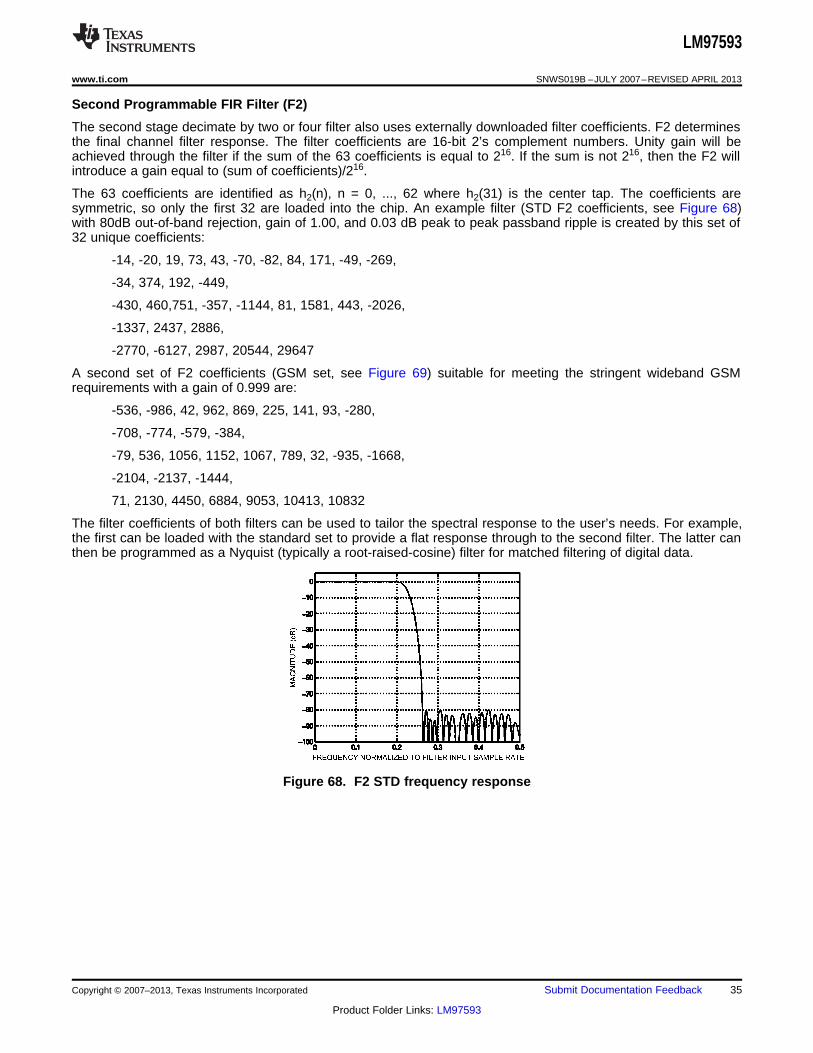
Second Programmable FIR Filter (F2)
The second stage decimate by two or four filter also uses externally downloaded filter coefficients. F2 determinesthe final channel filter response. The filter coefficients are 16-bit 2’s complement numbers. Unity gain will beachieved through the filter if the sum of the 63 coefficients is equal to 216. If the sum is not 216, then the F2 willintroduce a gain equal to (sum of coefficients)/216.
The 63 coefficients are identified as h2(n), n = 0, ..., 62 where h2(31) is the center tap. The coefficients aresymmetric, so only the first 32 are loaded into the chip. An example filter (STD F2 coefficients, see Figure 68)with 80dB out-of-band rejection, gain of 1.00, and 0.03 dB peak to peak passband ripple is created by this set of32 unique coefficients:
-14, -20, 19, 73, 43, -70, -82, 84, 171, -49, -269,
-34, 374, 192, -449,
-430, 460,751, -357, -1144, 81, 1581, 443, -2026,
-1337, 2437, 2886,
-2770, -6127, 2987, 20544, 29647
A second set of F2 coefficients (GSM set, see Figure 69) suitable for meeting the stringent wideband GSMrequirements with a gain of 0.999 are:
-536, -986, 42, 962, 869, 225, 141, 93, -280,
-708, -774, -579, -384,
-79, 536, 1056, 1152, 1067, 789, 32, -935, -1668,
-2104, -2137, -1444,
71, 2130, 4450, 6884, 9053, 10413, 10832
The filter coefficients of both filters can be used to tailor the spectral response to the user’s needs. For example,the first can be loaded with the standard set to provide a flat response through to the second filter. The latter canthen be programmed as a Nyquist (typically a root-raised-cosine) filter for matched filtering of digital data.
Figure 68. F2 STD frequency response
Copyright © 2007–2013, Texas Instruments Incorporated Submit Documentation Feedback 35
Product Folder Links: LM97593
LM97593
SNWS019B –JULY 2007–REVISED APRIL 2013 www.ti.com
Figure 69. F2 GSM frequency response
The complete channel filter response for standard coefficients is shown in Figure 70. Passband flatness is shownin Figure 71. The complete filter response for GSM coefficients is shown in Figure 72. GSM Passband flatness isshown in Figure 73.
The mask shown in Figure 72 is derived from the ETSI GSM 5.05 specifications for a normal BasestationTransceiver (BTS). For interferers, 9dB was added to the carrier to interference (C/I) ratios. For blockers, 9dBwas added to the difference between the blocker level and 3dB above the reference sensitivity level.
Channel Bandwidth vs. Sample Rate
When the LM97593 is used for GSM systems, a bandwidth of about 200kHz is desired. With a sample rate of52MHz, the total decimation of 192 provides the desired 270.833kHz output sample rate. This output sample ratein combination with the FIR filter coefficients create the desired channel bandwidth. If the sample rate isincreased to 65MHz, the decimation must also be increased to 65MHz/270.833kHz or 240.
Figure 70. CIC, F1, & F2 STD frequency response
36 Submit Documentation Feedback Copyright © 2007–2013, Texas Instruments Incorporated
Product Folder Links: LM97593
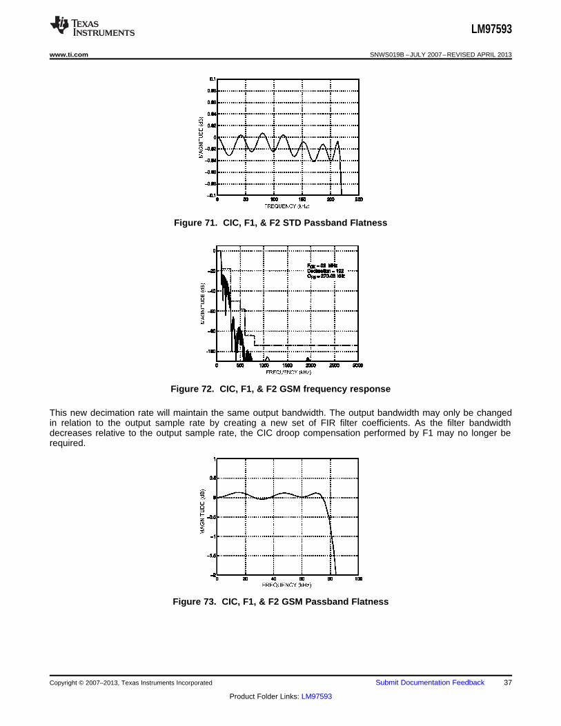
LM97593
www.ti.com SNWS019B –JULY 2007–REVISED APRIL 2013
Figure 71. CIC, F1, & F2 STD Passband Flatness
Figure 72. CIC, F1, & F2 GSM frequency response
This new decimation rate will maintain the same output bandwidth. The output bandwidth may only be changedin relation to the output sample rate by creating a new set of FIR filter coefficients. As the filter bandwidthdecreases relative to the output sample rate, the CIC droop compensation performed by F1 may no longer berequired.
Figure 73. CIC, F1, & F2 GSM Passband Flatness
Copyright © 2007–2013, Texas Instruments Incorporated Submit Documentation Feedback 37
Product Folder Links: LM97593
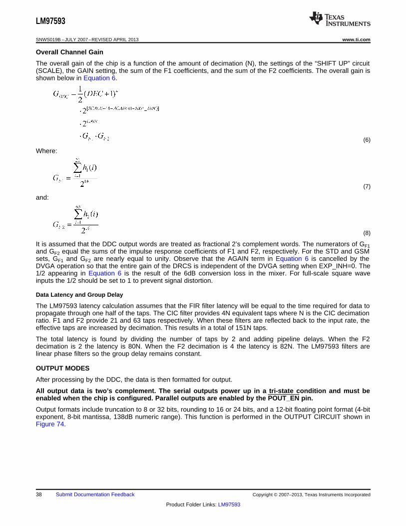
LM97593
SNWS019B –JULY 2007–REVISED APRIL 2013 www.ti.com
Overall Channel Gain
The overall gain of the chip is a function of the amount of decimation (N), the settings of the “SHIFT UP” circuit(SCALE), the GAIN setting, the sum of the F1 coefficients, and the sum of the F2 coefficients. The overall gain isshown below in Equation 6.
(6)
Where:
(7)
and:
(8)
It is assumed that the DDC output words are treated as fractional 2’s complement words. The numerators of GF1and GF2 equal the sums of the impulse response coefficients of F1 and F2, respectively. For the STD and GSMsets, GF1 and GF2 are nearly equal to unity. Observe that the AGAIN term in Equation 6 is cancelled by theDVGA operation so that the entire gain of the DRCS is independent of the DVGA setting when EXP_INH=0. The1/2 appearing in Equation 6 is the result of the 6dB conversion loss in the mixer. For full-scale square waveinputs the 1/2 should be set to 1 to prevent signal distortion.
Data Latency and Group Delay
The LM97593 latency calculation assumes that the FIR filter latency will be equal to the time required for data topropagate through one half of the taps. The CIC filter provides 4N equivalent taps where N is the CIC decimationratio. F1 and F2 provide 21 and 63 taps respectively. When these filters are reflected back to the input rate, theeffective taps are increased by decimation. This results in a total of 151N taps.
The total latency is found by dividing the number of taps by 2 and adding pipeline delays. When the F2decimation is 2 the latency is 80N. When the F2 decimation is 4 the latency is 82N. The LM97593 filters arelinear phase filters so the group delay remains constant.
OUTPUT MODES
After processing by the DDC, the data is then formatted for output.
All output data is two’s complement. The serial outputs power up in a tri-state condition and must beenabled when the chip is configured. Parallel outputs are enabled by the POUT_EN pin.
Output formats include truncation to 8 or 32 bits, rounding to 16 or 24 bits, and a 12-bit floating point format (4-bitexponent, 8-bit mantissa, 138dB numeric range). This function is performed in the OUTPUT CIRCUIT shown inFigure 74.
38 Submit Documentation Feedback Copyright © 2007–2013, Texas Instruments Incorporated
Product Folder Links: LM97593
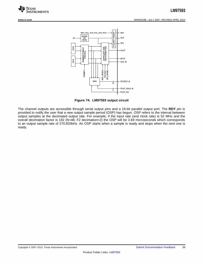
LM97593
www.ti.com SNWS019B –JULY 2007–REVISED APRIL 2013
Figure 74. LM97593 output circuit
The channel outputs are accessible through serial output pins and a 16-bit parallel output port. The RDY pin isprovided to notify the user that a new output sample period (OSP) has begun. OSP refers to the interval betweenoutput samples at the decimated output rate. For example, if the input rate (and clock rate) is 52 MHz and theoverall decimation factor is 192 (N=48, F2 decimation=2) the OSP will be 3.69 microseconds which correspondsto an output sample rate of 270.833kHz. An OSP starts when a sample is ready and stops when the next one isready.
Copyright © 2007–2013, Texas Instruments Incorporated Submit Documentation Feedback 39
Product Folder Links: LM97593
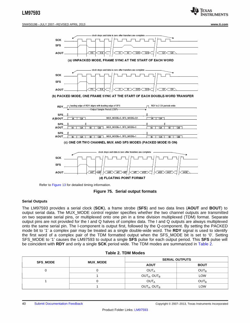
LM97593
SNWS019B –JULY 2007–REVISED APRIL 2013 www.ti.com
Refer to Figure 13 for detailed timing information.
Figure 75. Serial output formats
Serial Outputs
The LM97593 provides a serial clock (SCK), a frame strobe (SFS) and two data lines (AOUT and BOUT) tooutput serial data. The MUX_MODE control register specifies whether the two channel outputs are transmittedon two separate serial pins, or multiplexed onto one pin in a time division multiplexed (TDM) format. Separateoutput pins are not provided for the I and Q halves of complex data. The I and Q outputs are always multiplexedonto the same serial pin. The I-component is output first, followed by the Q-component. By setting the PACKEDmode bit to ‘1’ a complex pair may be treated as a single double-wide word. The RDY signal is used to identifythe first word of a complex pair of the TDM formatted output when the SFS_MODE bit is set to ‘0’. SettingSFS_MODE to ‘1’ causes the LM97593 to output a single SFS pulse for each output period. This SFS pulse willbe coincident with RDY and only a single SCK period wide. The TDM modes are summarized in Table 2.
Table 2. TDM Modes
SERIAL OUTPUTSSFS_MODE MUX_MODE
AOUT BOUT
0 0 OUTA OUTB
1 OUTA, OUTB LOW
1 0 OUTA OUTB
1 OUTA, OUTB LOW
40 Submit Documentation Feedback Copyright © 2007–2013, Texas Instruments Incorporated
Product Folder Links: LM97593
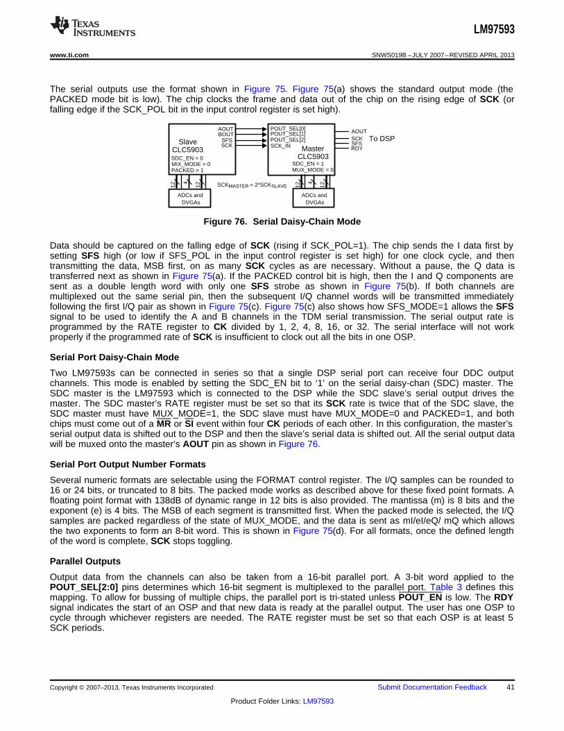
AOUTSCKSFSRDY
POUT_SEL[0]
SCK_IN
POUT_SEL[1]POUT_SEL[2]
SDC_EN = 1MUX_MODE = 0
MasterCLC5903
To DSP
ADCs andDVGAs
SCKMASTER = 2*SCKSLAVE
AOUTBOUT
SFSSCK
SDC_EN = 0MIX_MODE = 0PACKED = 1
12 12
4
SlaveCLC5903
12 12
4
ADCs andDVGAs
LM97593
www.ti.com SNWS019B –JULY 2007–REVISED APRIL 2013
The serial outputs use the format shown in Figure 75. Figure 75(a) shows the standard output mode (thePACKED mode bit is low). The chip clocks the frame and data out of the chip on the rising edge of SCK (orfalling edge if the SCK_POL bit in the input control register is set high).
Figure 76. Serial Daisy-Chain Mode
Data should be captured on the falling edge of SCK (rising if SCK_POL=1). The chip sends the I data first bysetting SFS high (or low if SFS_POL in the input control register is set high) for one clock cycle, and thentransmitting the data, MSB first, on as many SCK cycles as are necessary. Without a pause, the Q data istransferred next as shown in Figure 75(a). If the PACKED control bit is high, then the I and Q components aresent as a double length word with only one SFS strobe as shown in Figure 75(b). If both channels aremultiplexed out the same serial pin, then the subsequent I/Q channel words will be transmitted immediatelyfollowing the first I/Q pair as shown in Figure 75(c). Figure 75(c) also shows how SFS_MODE=1 allows the SFSsignal to be used to identify the A and B channels in the TDM serial transmission. The serial output rate isprogrammed by the RATE register to CK divided by 1, 2, 4, 8, 16, or 32. The serial interface will not workproperly if the programmed rate of SCK is insufficient to clock out all the bits in one OSP.
Serial Port Daisy-Chain Mode
Two LM97593s can be connected in series so that a single DSP serial port can receive four DDC outputchannels. This mode is enabled by setting the SDC_EN bit to ‘1’ on the serial daisy-chan (SDC) master. TheSDC master is the LM97593 which is connected to the DSP while the SDC slave’s serial output drives themaster. The SDC master’s RATE register must be set so that its SCK rate is twice that of the SDC slave, theSDC master must have MUX_MODE=1, the SDC slave must have MUX_MODE=0 and PACKED=1, and bothchips must come out of a MR or SI event within four CK periods of each other. In this configuration, the master’sserial output data is shifted out to the DSP and then the slave’s serial data is shifted out. All the serial output datawill be muxed onto the master’s AOUT pin as shown in Figure 76.
Serial Port Output Number Formats
Several numeric formats are selectable using the FORMAT control register. The I/Q samples can be rounded to16 or 24 bits, or truncated to 8 bits. The packed mode works as described above for these fixed point formats. Afloating point format with 138dB of dynamic range in 12 bits is also provided. The mantissa (m) is 8 bits and theexponent (e) is 4 bits. The MSB of each segment is transmitted first. When the packed mode is selected, the I/Qsamples are packed regardless of the state of MUX_MODE, and the data is sent as mI/eI/eQ/ mQ which allowsthe two exponents to form an 8-bit word. This is shown in Figure 75(d). For all formats, once the defined lengthof the word is complete, SCK stops toggling.
Parallel Outputs
Output data from the channels can also be taken from a 16-bit parallel port. A 3-bit word applied to thePOUT_SEL[2:0] pins determines which 16-bit segment is multiplexed to the parallel port. Table 3 defines thismapping. To allow for bussing of multiple chips, the parallel port is tri-stated unless POUT_EN is low. The RDYsignal indicates the start of an OSP and that new data is ready at the parallel output. The user has one OSP tocycle through whichever registers are needed. The RATE register must be set so that each OSP is at least 5SCK periods.
Copyright © 2007–2013, Texas Instruments Incorporated Submit Documentation Feedback 41
Product Folder Links: LM97593
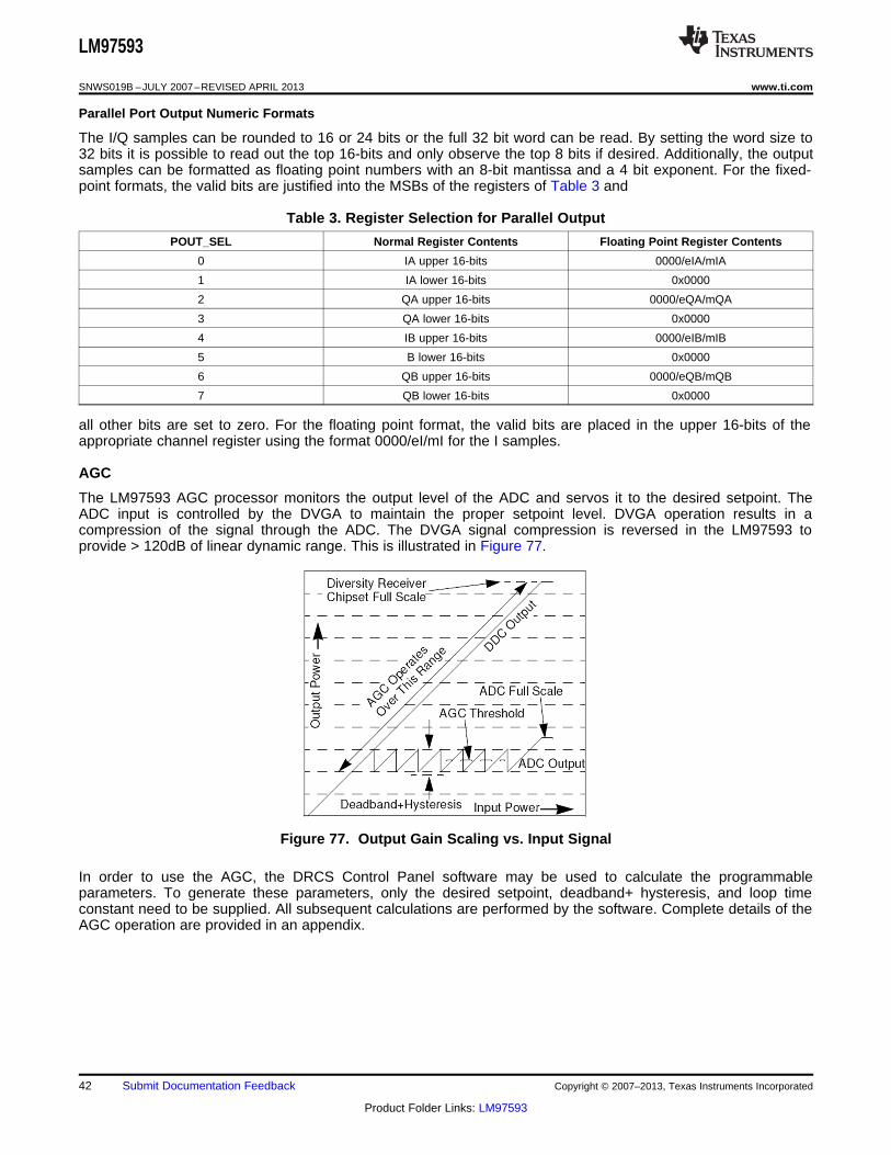
LM97593
SNWS019B –JULY 2007–REVISED APRIL 2013 www.ti.com
Parallel Port Output Numeric Formats
The I/Q samples can be rounded to 16 or 24 bits or the full 32 bit word can be read. By setting the word size to32 bits it is possible to read out the top 16-bits and only observe the top 8 bits if desired. Additionally, the outputsamples can be formatted as floating point numbers with an 8-bit mantissa and a 4 bit exponent. For the fixed-point formats, the valid bits are justified into the MSBs of the registers of Table 3 and
Table 3. Register Selection for Parallel Output
POUT_SEL Normal Register Contents Floating Point Register Contents
0 IA upper 16-bits 0000/eIA/mIA
1 IA lower 16-bits 0x0000
2 QA upper 16-bits 0000/eQA/mQA
3 QA lower 16-bits 0x0000
4 IB upper 16-bits 0000/eIB/mIB
5 B lower 16-bits 0x0000
6 QB upper 16-bits 0000/eQB/mQB
7 QB lower 16-bits 0x0000
all other bits are set to zero. For the floating point format, the valid bits are placed in the upper 16-bits of theappropriate channel register using the format 0000/eI/mI for the I samples.
AGC
The LM97593 AGC processor monitors the output level of the ADC and servos it to the desired setpoint. TheADC input is controlled by the DVGA to maintain the proper setpoint level. DVGA operation results in acompression of the signal through the ADC. The DVGA signal compression is reversed in the LM97593 toprovide > 120dB of linear dynamic range. This is illustrated in Figure 77.
Figure 77. Output Gain Scaling vs. Input Signal
In order to use the AGC, the DRCS Control Panel software may be used to calculate the programmableparameters. To generate these parameters, only the desired setpoint, deadband+ hysteresis, and loop timeconstant need to be supplied. All subsequent calculations are performed by the software. Complete details of theAGC operation are provided in an appendix.
42 Submit Documentation Feedback Copyright © 2007–2013, Texas Instruments Incorporated
Product Folder Links: LM97593
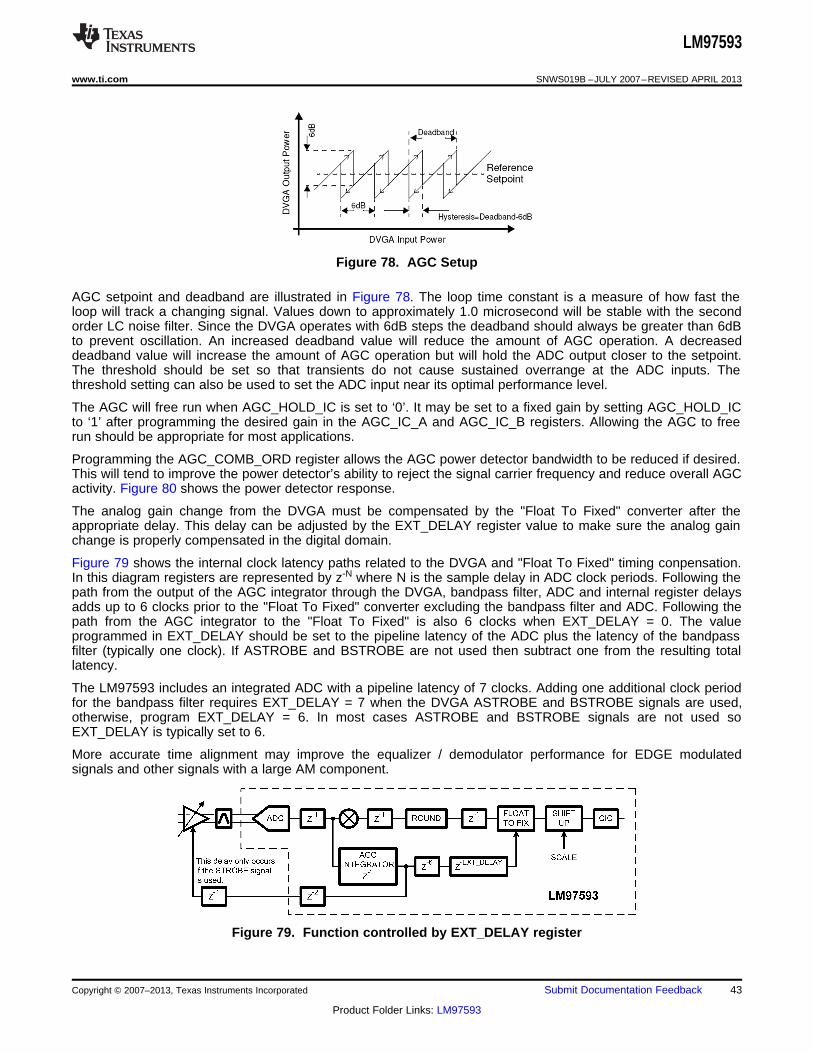
LM97593
www.ti.com SNWS019B –JULY 2007–REVISED APRIL 2013
Figure 78. AGC Setup
AGC setpoint and deadband are illustrated in Figure 78. The loop time constant is a measure of how fast theloop will track a changing signal. Values down to approximately 1.0 microsecond will be stable with the secondorder LC noise filter. Since the DVGA operates with 6dB steps the deadband should always be greater than 6dBto prevent oscillation. An increased deadband value will reduce the amount of AGC operation. A decreaseddeadband value will increase the amount of AGC operation but will hold the ADC output closer to the setpoint.The threshold should be set so that transients do not cause sustained overrange at the ADC inputs. Thethreshold setting can also be used to set the ADC input near its optimal performance level.
The AGC will free run when AGC_HOLD_IC is set to ‘0’. It may be set to a fixed gain by setting AGC_HOLD_ICto ‘1’ after programming the desired gain in the AGC_IC_A and AGC_IC_B registers. Allowing the AGC to freerun should be appropriate for most applications.
Programming the AGC_COMB_ORD register allows the AGC power detector bandwidth to be reduced if desired.This will tend to improve the power detector’s ability to reject the signal carrier frequency and reduce overall AGCactivity. Figure 80 shows the power detector response.
The analog gain change from the DVGA must be compensated by the "Float To Fixed" converter after theappropriate delay. This delay can be adjusted by the EXT_DELAY register value to make sure the analog gainchange is properly compensated in the digital domain.
Figure 79 shows the internal clock latency paths related to the DVGA and "Float To Fixed" timing conpensation.In this diagram registers are represented by z-N where N is the sample delay in ADC clock periods. Following thepath from the output of the AGC integrator through the DVGA, bandpass filter, ADC and internal register delaysadds up to 6 clocks prior to the "Float To Fixed" converter excluding the bandpass filter and ADC. Following thepath from the AGC integrator to the "Float To Fixed" is also 6 clocks when EXT_DELAY = 0. The valueprogrammed in EXT_DELAY should be set to the pipeline latency of the ADC plus the latency of the bandpassfilter (typically one clock). If ASTROBE and BSTROBE are not used then subtract one from the resulting totallatency.
The LM97593 includes an integrated ADC with a pipeline latency of 7 clocks. Adding one additional clock periodfor the bandpass filter requires EXT_DELAY = 7 when the DVGA ASTROBE and BSTROBE signals are used,otherwise, program EXT_DELAY = 6. In most cases ASTROBE and BSTROBE signals are not used soEXT_DELAY is typically set to 6.
More accurate time alignment may improve the equalizer / demodulator performance for EDGE modulatedsignals and other signals with a large AM component.
Figure 79. Function controlled by EXT_DELAY register
Copyright © 2007–2013, Texas Instruments Incorporated Submit Documentation Feedback 43
Product Folder Links: LM97593
LM97593
SNWS019B –JULY 2007–REVISED APRIL 2013 www.ti.com
POWER MANAGEMENT
The LM97593 can be placed in a low power (static) state by stopping the input clock and setting the PD pin high.To prevent this from placing the LM97593 into unexpected states, the SI pin of the LM97593 should be assertedprior to disabling the input clock and held asserted until the input clock has returned to a stable condition.
TESTABILITY
JTAG Boundary Scan
The LM97593 supports IEEE 1149.1 compliant JTAG Boundary Scan for the I/O's. The following pins are used:
TRST (test reset)
TMS (test mode select)
TDI (test data in)
TDO (test data out)
TCK (test clock)
The following JTAG instructions are supported:
Instruction Description
BYPASS Connects TDI directly to TDO
EXTEST Enables the test access port controller to drive the outputs
IDCODE Connects the 32-bit ID register to TDO
SAMPLE/PRELOAD Allows the test access port to sample the device inputs and preloadtest output data
HIGHZ Tri-states the outputs
The JTAG Boundary Scan can be used to verify printed circuit board continuity at the system level.
Test Register
The user is able to program a value into TEST_REG and substitute this for the normal channel inputs from theAIN/ BIN pins by selecting it with the crossbar. With the NCO frequency set to zero this allows the DDCs and theoutput interface of the chip to be verified. Also, the AGC loop can be opened by setting AGC_HOLD_IC high andsetting the gain of the DVGA by programming the appropriate value into the AGC_IC_A/B register.
Debug Access Port
Real-time access to the following signals is provided by configuring the control interface debug register:• NCO sine and cosine outputs• data after round following mixers• data before F1 and F2• data after CIC filter within the AGC
The access points are multiplexed to a 20-bit parallel output port which is created from signal pins POUT[15:0],AOUT, BOUT, SFS, and RDY according to the table below:
Normal Mode Pin Debug Mode Pin
POUT[15:0] DEBUG[19:4]
RDY DEBUG[3]
SFS DEBUG[2]
AOUT DEBUG[1]
BOUT DEBUG[0]
44 Submit Documentation Feedback Copyright © 2007–2013, Texas Instruments Incorporated
Product Folder Links: LM97593
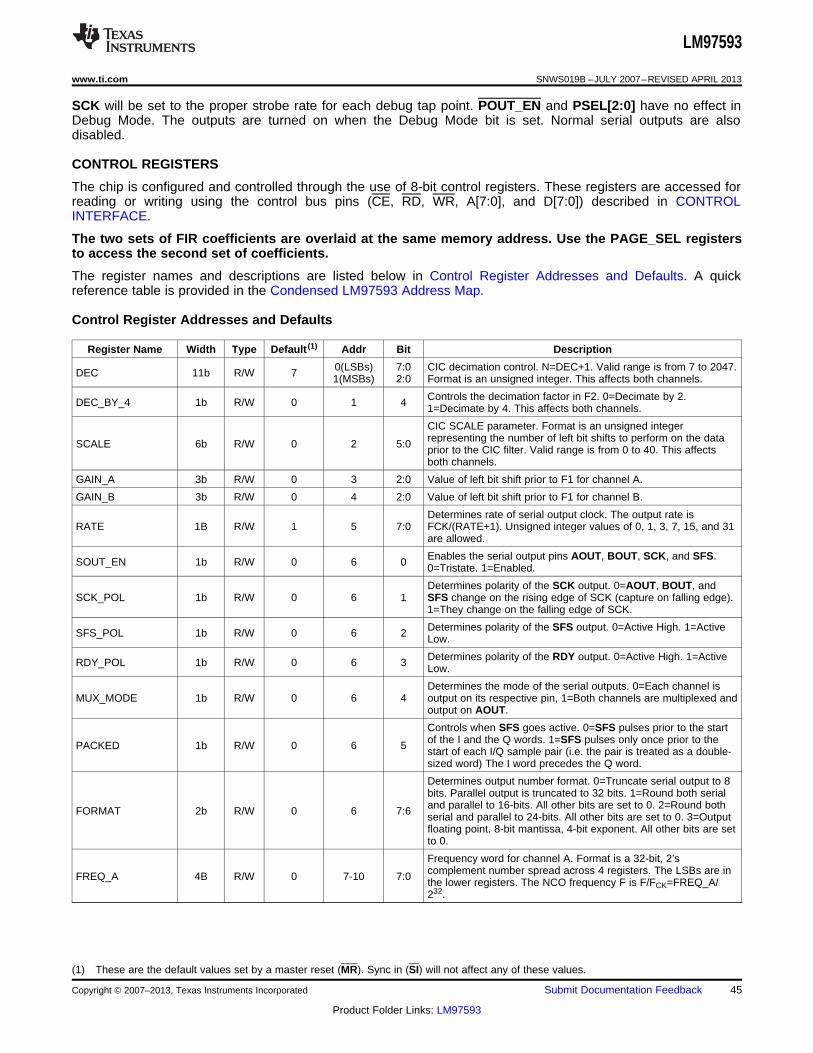
LM97593
www.ti.com SNWS019B –JULY 2007–REVISED APRIL 2013
SCK will be set to the proper strobe rate for each debug tap point. POUT_EN and PSEL[2:0] have no effect inDebug Mode. The outputs are turned on when the Debug Mode bit is set. Normal serial outputs are alsodisabled.
CONTROL REGISTERS
The chip is configured and controlled through the use of 8-bit control registers. These registers are accessed forreading or writing using the control bus pins (CE, RD, WR, A[7:0], and D[7:0]) described in CONTROLINTERFACE.
The two sets of FIR coefficients are overlaid at the same memory address. Use the PAGE_SEL registersto access the second set of coefficients.
The register names and descriptions are listed below in Control Register Addresses and Defaults. A quickreference table is provided in the Condensed LM97593 Address Map.
Control Register Addresses and Defaults
Register Name Width Type Default (1) Addr Bit Description
0(LSBs) 7:0 CIC decimation control. N=DEC+1. Valid range is from 7 to 2047.DEC 11b R/W 7 1(MSBs) 2:0 Format is an unsigned integer. This affects both channels.
Controls the decimation factor in F2. 0=Decimate by 2.DEC_BY_4 1b R/W 0 1 4 1=Decimate by 4. This affects both channels.
CIC SCALE parameter. Format is an unsigned integerrepresenting the number of left bit shifts to perform on the dataSCALE 6b R/W 0 2 5:0 prior to the CIC filter. Valid range is from 0 to 40. This affectsboth channels.
GAIN_A 3b R/W 0 3 2:0 Value of left bit shift prior to F1 for channel A.
GAIN_B 3b R/W 0 4 2:0 Value of left bit shift prior to F1 for channel B.
Determines rate of serial output clock. The output rate isRATE 1B R/W 1 5 7:0 FCK/(RATE+1). Unsigned integer values of 0, 1, 3, 7, 15, and 31
are allowed.
Enables the serial output pins AOUT, BOUT, SCK, and SFS.SOUT_EN 1b R/W 0 6 0 0=Tristate. 1=Enabled.
Determines polarity of the SCK output. 0=AOUT, BOUT, andSCK_POL 1b R/W 0 6 1 SFS change on the rising edge of SCK (capture on falling edge).
1=They change on the falling edge of SCK.
Determines polarity of the SFS output. 0=Active High. 1=ActiveSFS_POL 1b R/W 0 6 2 Low.
Determines polarity of the RDY output. 0=Active High. 1=ActiveRDY_POL 1b R/W 0 6 3 Low.
Determines the mode of the serial outputs. 0=Each channel isMUX_MODE 1b R/W 0 6 4 output on its respective pin, 1=Both channels are multiplexed and
output on AOUT.
Controls when SFS goes active. 0=SFS pulses prior to the startof the I and the Q words. 1=SFS pulses only once prior to thePACKED 1b R/W 0 6 5 start of each I/Q sample pair (i.e. the pair is treated as a double-sized word) The I word precedes the Q word.
Determines output number format. 0=Truncate serial output to 8bits. Parallel output is truncated to 32 bits. 1=Round both serialand parallel to 16-bits. All other bits are set to 0. 2=Round bothFORMAT 2b R/W 0 6 7:6 serial and parallel to 24-bits. All other bits are set to 0. 3=Outputfloating point. 8-bit mantissa, 4-bit exponent. All other bits are setto 0.
Frequency word for channel A. Format is a 32-bit, 2’scomplement number spread across 4 registers. The LSBs are inFREQ_A 4B R/W 0 7-10 7:0 the lower registers. The NCO frequency F is F/FCK=FREQ_A/232.
(1) These are the default values set by a master reset (MR). Sync in (SI) will not affect any of these values.
Copyright © 2007–2013, Texas Instruments Incorporated Submit Documentation Feedback 45
Product Folder Links: LM97593
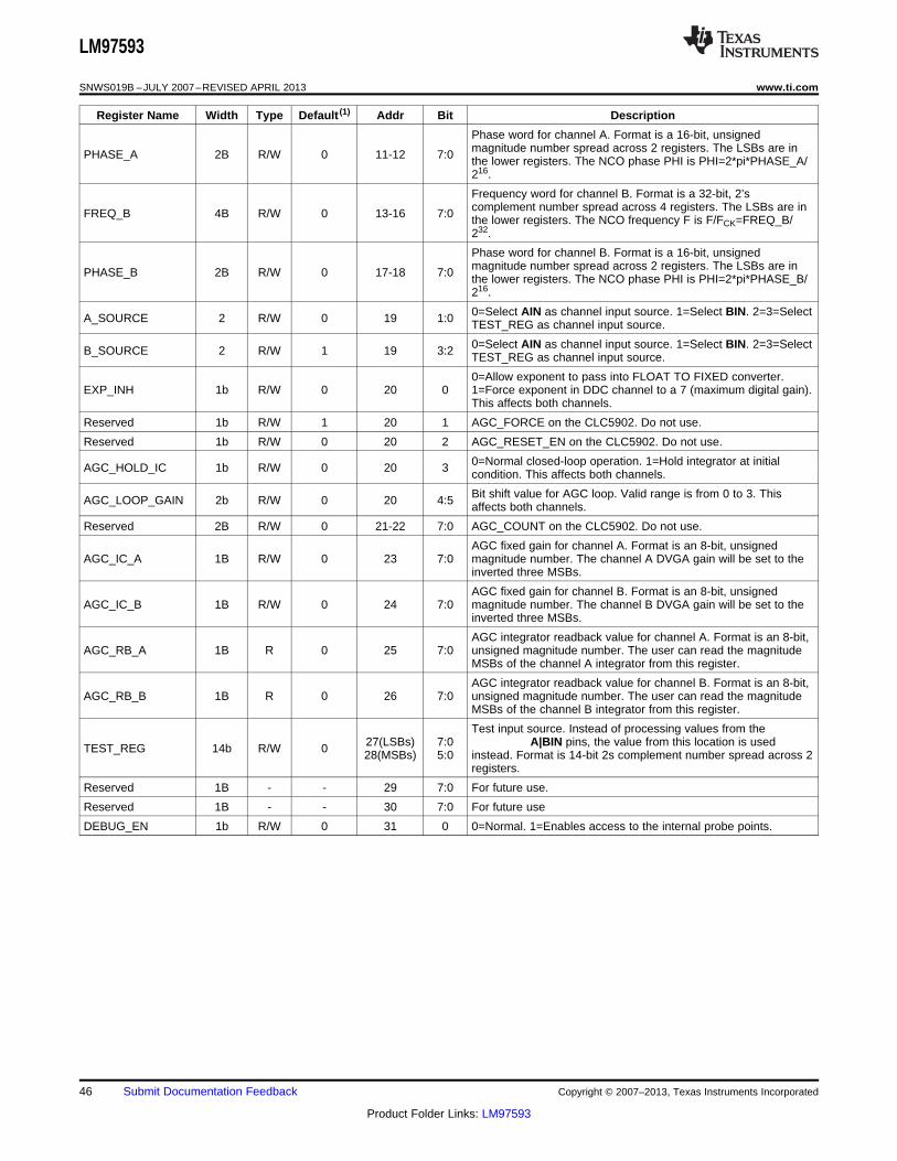
LM97593
SNWS019B –JULY 2007–REVISED APRIL 2013 www.ti.com
Register Name Width Type Default (1) Addr Bit Description
Phase word for channel A. Format is a 16-bit, unsignedmagnitude number spread across 2 registers. The LSBs are inPHASE_A 2B R/W 0 11-12 7:0 the lower registers. The NCO phase PHI is PHI=2*pi*PHASE_A/216.
Frequency word for channel B. Format is a 32-bit, 2’scomplement number spread across 4 registers. The LSBs are inFREQ_B 4B R/W 0 13-16 7:0 the lower registers. The NCO frequency F is F/FCK=FREQ_B/232.
Phase word for channel B. Format is a 16-bit, unsignedmagnitude number spread across 2 registers. The LSBs are inPHASE_B 2B R/W 0 17-18 7:0 the lower registers. The NCO phase PHI is PHI=2*pi*PHASE_B/216.
0=Select AIN as channel input source. 1=Select BIN. 2=3=SelectA_SOURCE 2 R/W 0 19 1:0 TEST_REG as channel input source.
0=Select AIN as channel input source. 1=Select BIN. 2=3=SelectB_SOURCE 2 R/W 1 19 3:2 TEST_REG as channel input source.
0=Allow exponent to pass into FLOAT TO FIXED converter.EXP_INH 1b R/W 0 20 0 1=Force exponent in DDC channel to a 7 (maximum digital gain).
This affects both channels.
Reserved 1b R/W 1 20 1 AGC_FORCE on the CLC5902. Do not use.
Reserved 1b R/W 0 20 2 AGC_RESET_EN on the CLC5902. Do not use.
0=Normal closed-loop operation. 1=Hold integrator at initialAGC_HOLD_IC 1b R/W 0 20 3 condition. This affects both channels.
Bit shift value for AGC loop. Valid range is from 0 to 3. ThisAGC_LOOP_GAIN 2b R/W 0 20 4:5 affects both channels.
Reserved 2B R/W 0 21-22 7:0 AGC_COUNT on the CLC5902. Do not use.
AGC fixed gain for channel A. Format is an 8-bit, unsignedAGC_IC_A 1B R/W 0 23 7:0 magnitude number. The channel A DVGA gain will be set to the
inverted three MSBs.
AGC fixed gain for channel B. Format is an 8-bit, unsignedAGC_IC_B 1B R/W 0 24 7:0 magnitude number. The channel B DVGA gain will be set to the
inverted three MSBs.
AGC integrator readback value for channel A. Format is an 8-bit,AGC_RB_A 1B R 0 25 7:0 unsigned magnitude number. The user can read the magnitude
MSBs of the channel A integrator from this register.
AGC integrator readback value for channel B. Format is an 8-bit,AGC_RB_B 1B R 0 26 7:0 unsigned magnitude number. The user can read the magnitude
MSBs of the channel B integrator from this register.
Test input source. Instead of processing values from the27(LSBs) 7:0 A|BIN pins, the value from this location is usedTEST_REG 14b R/W 0 28(MSBs) 5:0 instead. Format is 14-bit 2s complement number spread across 2
registers.
Reserved 1B - - 29 7:0 For future use.
Reserved 1B - - 30 7:0 For future use
DEBUG_EN 1b R/W 0 31 0 0=Normal. 1=Enables access to the internal probe points.
46 Submit Documentation Feedback Copyright © 2007–2013, Texas Instruments Incorporated
Product Folder Links: LM97593
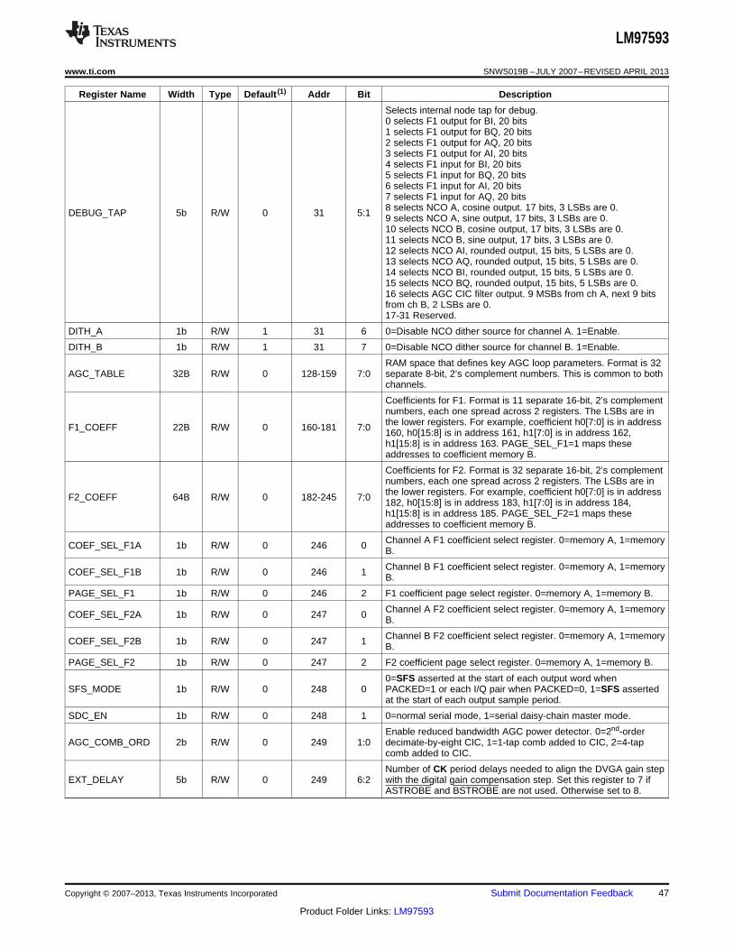
LM97593
www.ti.com SNWS019B –JULY 2007–REVISED APRIL 2013
Register Name Width Type Default (1) Addr Bit Description
Selects internal node tap for debug.0 selects F1 output for BI, 20 bits1 selects F1 output for BQ, 20 bits2 selects F1 output for AQ, 20 bits3 selects F1 output for AI, 20 bits4 selects F1 input for BI, 20 bits5 selects F1 input for BQ, 20 bits6 selects F1 input for AI, 20 bits7 selects F1 input for AQ, 20 bits8 selects NCO A, cosine output. 17 bits, 3 LSBs are 0.DEBUG_TAP 5b R/W 0 31 5:1 9 selects NCO A, sine output, 17 bits, 3 LSBs are 0.10 selects NCO B, cosine output, 17 bits, 3 LSBs are 0.11 selects NCO B, sine output, 17 bits, 3 LSBs are 0.12 selects NCO AI, rounded output, 15 bits, 5 LSBs are 0.13 selects NCO AQ, rounded output, 15 bits, 5 LSBs are 0.14 selects NCO BI, rounded output, 15 bits, 5 LSBs are 0.15 selects NCO BQ, rounded output, 15 bits, 5 LSBs are 0.16 selects AGC CIC filter output. 9 MSBs from ch A, next 9 bitsfrom ch B, 2 LSBs are 0.17-31 Reserved.
DITH_A 1b R/W 1 31 6 0=Disable NCO dither source for channel A. 1=Enable.
DITH_B 1b R/W 1 31 7 0=Disable NCO dither source for channel B. 1=Enable.
RAM space that defines key AGC loop parameters. Format is 32AGC_TABLE 32B R/W 0 128-159 7:0 separate 8-bit, 2’s complement numbers. This is common to both
channels.
Coefficients for F1. Format is 11 separate 16-bit, 2’s complementnumbers, each one spread across 2 registers. The LSBs are inthe lower registers. For example, coefficient h0[7:0] is in addressF1_COEFF 22B R/W 0 160-181 7:0 160, h0[15:8] is in address 161, h1[7:0] is in address 162,h1[15:8] is in address 163. PAGE_SEL_F1=1 maps theseaddresses to coefficient memory B.
Coefficients for F2. Format is 32 separate 16-bit, 2’s complementnumbers, each one spread across 2 registers. The LSBs are inthe lower registers. For example, coefficient h0[7:0] is in addressF2_COEFF 64B R/W 0 182-245 7:0 182, h0[15:8] is in address 183, h1[7:0] is in address 184,h1[15:8] is in address 185. PAGE_SEL_F2=1 maps theseaddresses to coefficient memory B.
Channel A F1 coefficient select register. 0=memory A, 1=memoryCOEF_SEL_F1A 1b R/W 0 246 0 B.
Channel B F1 coefficient select register. 0=memory A, 1=memoryCOEF_SEL_F1B 1b R/W 0 246 1 B.
PAGE_SEL_F1 1b R/W 0 246 2 F1 coefficient page select register. 0=memory A, 1=memory B.
Channel A F2 coefficient select register. 0=memory A, 1=memoryCOEF_SEL_F2A 1b R/W 0 247 0 B.
Channel B F2 coefficient select register. 0=memory A, 1=memoryCOEF_SEL_F2B 1b R/W 0 247 1 B.
PAGE_SEL_F2 1b R/W 0 247 2 F2 coefficient page select register. 0=memory A, 1=memory B.
0=SFS asserted at the start of each output word whenSFS_MODE 1b R/W 0 248 0 PACKED=1 or each I/Q pair when PACKED=0, 1=SFS asserted
at the start of each output sample period.
SDC_EN 1b R/W 0 248 1 0=normal serial mode, 1=serial daisy-chain master mode.
Enable reduced bandwidth AGC power detector. 0=2nd-orderAGC_COMB_ORD 2b R/W 0 249 1:0 decimate-by-eight CIC, 1=1-tap comb added to CIC, 2=4-tap
comb added to CIC.
Number of CK period delays needed to align the DVGA gain stepEXT_DELAY 5b R/W 0 249 6:2 with the digital gain compensation step. Set this register to 7 if
ASTROBE and BSTROBE are not used. Otherwise set to 8.
Copyright © 2007–2013, Texas Instruments Incorporated Submit Documentation Feedback 47
Product Folder Links: LM97593
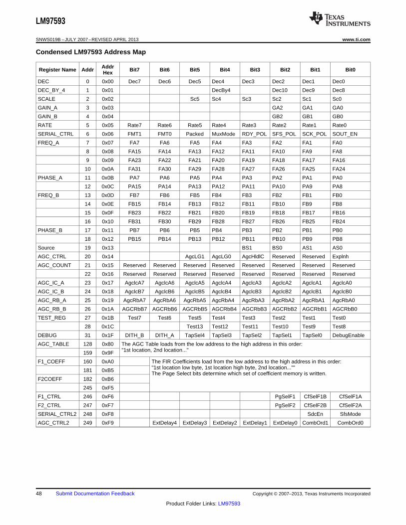
LM97593
SNWS019B –JULY 2007–REVISED APRIL 2013 www.ti.com
Condensed LM97593 Address Map
AddrRegister Name Addr Bit7 Bit6 Bit5 Bit4 Bit3 Bit2 Bit1 Bit0Hex
DEC 0 0x00 Dec7 Dec6 Dec5 Dec4 Dec3 Dec2 Dec1 Dec0
DEC_BY_4 1 0x01 DecBy4 Dec10 Dec9 Dec8
SCALE 2 0x02 Sc5 Sc4 Sc3 Sc2 Sc1 Sc0
GAIN_A 3 0x03 GA2 GA1 GA0
GAIN_B 4 0x04 GB2 GB1 GB0
RATE 5 0x05 Rate7 Rate6 Rate5 Rate4 Rate3 Rate2 Rate1 Rate0
SERIAL_CTRL 6 0x06 FMT1 FMT0 Packed MuxMode RDY_POL SFS_POL SCK_POL SOUT_EN
FREQ_A 7 0x07 FA7 FA6 FA5 FA4 FA3 FA2 FA1 FA0
8 0x08 FA15 FA14 FA13 FA12 FA11 FA10 FA9 FA8
9 0x09 FA23 FA22 FA21 FA20 FA19 FA18 FA17 FA16
10 0x0A FA31 FA30 FA29 FA28 FA27 FA26 FA25 FA24
PHASE_A 11 0x0B PA7 PA6 PA5 PA4 PA3 PA2 PA1 PA0
12 0x0C PA15 PA14 PA13 PA12 PA11 PA10 PA9 PA8
FREQ_B 13 0x0D FB7 FB6 FB5 FB4 FB3 FB2 FB1 FB0
14 0x0E FB15 FB14 FB13 FB12 FB11 FB10 FB9 FB8
15 0x0F FB23 FB22 FB21 FB20 FB19 FB18 FB17 FB16
16 0x10 FB31 FB30 FB29 FB28 FB27 FB26 FB25 FB24
PHASE_B 17 0x11 PB7 PB6 PB5 PB4 PB3 PB2 PB1 PB0
18 0x12 PB15 PB14 PB13 PB12 PB11 PB10 PB9 PB8
Source 19 0x13 BS1 BS0 AS1 AS0
AGC_CTRL 20 0x14 AgcLG1 AgcLG0 AgcHldlC Reserved Reserved Explnh
AGC_COUNT 21 0x15 Reserved Reserved Reserved Reserved Reserved Reserved Reserved Reserved
22 0x16 Reserved Reserved Reserved Reserved Reserved Reserved Reserved Reserved
AGC_IC_A 23 0x17 AgclcA7 AgclcA6 AgclcA5 AgclcA4 AgclcA3 AgclcA2 AgclcA1 AgclcA0
AGC_IC_B 24 0x18 AgclcB7 AgclcB6 AgclcB5 AgclcB4 AgclcB3 AgclcB2 AgclcB1 AgclcB0
AGC_RB_A 25 0x19 AgcRbA7 AgcRbA6 AgcRbA5 AgcRbA4 AgcRbA3 AgcRbA2 AgcRbA1 AgcRbA0
AGC_RB_B 26 0x1A AGCRbB7 AGCRbB6 AGCRbB5 AGCRbB4 AGCRbB3 AGCRbB2 AGCRbB1 AGCRbB0
TEST_REG 27 0x1B Test7 Test6 Test5 Test4 Test3 Test2 Test1 Test0
28 0x1C Test13 Test12 Test11 Test10 Test9 Test8
DEBUG 31 0x1F DITH_B DITH_A TapSel4 TapSel3 TapSel2 TapSel1 TapSel0 DebugEnable
AGC_TABLE 128 0x80 The AGC Table loads from the low address to the high address in this order:"1st location, 2nd location..."159 0x9F
F1_COEFF 160 0xA0 The FIR Coefficients load from the low address to the high address in this order:"1st location low byte, 1st location high byte, 2nd location...""181 0xB5The Page Select bits determine which set of coefficient memory is written.
F2COEFF 182 0xB6
245 0xF5
F1_CTRL 246 0xF6 PgSelF1 CfSelF1B CfSelF1A
F2_CTRL 247 0xF7 PgSelF2 CfSelF2B CfSelF2A
SERIAL_CTRL2 248 0xF8 SdcEn SfsMode
AGC_CTRL2 249 0xF9 ExtDelay4 ExtDelay3 ExtDelay2 ExtDelay1 ExtDelay0 CombOrd1 CombOrd0
48 Submit Documentation Feedback Copyright © 2007–2013, Texas Instruments Incorporated
Product Folder Links: LM97593
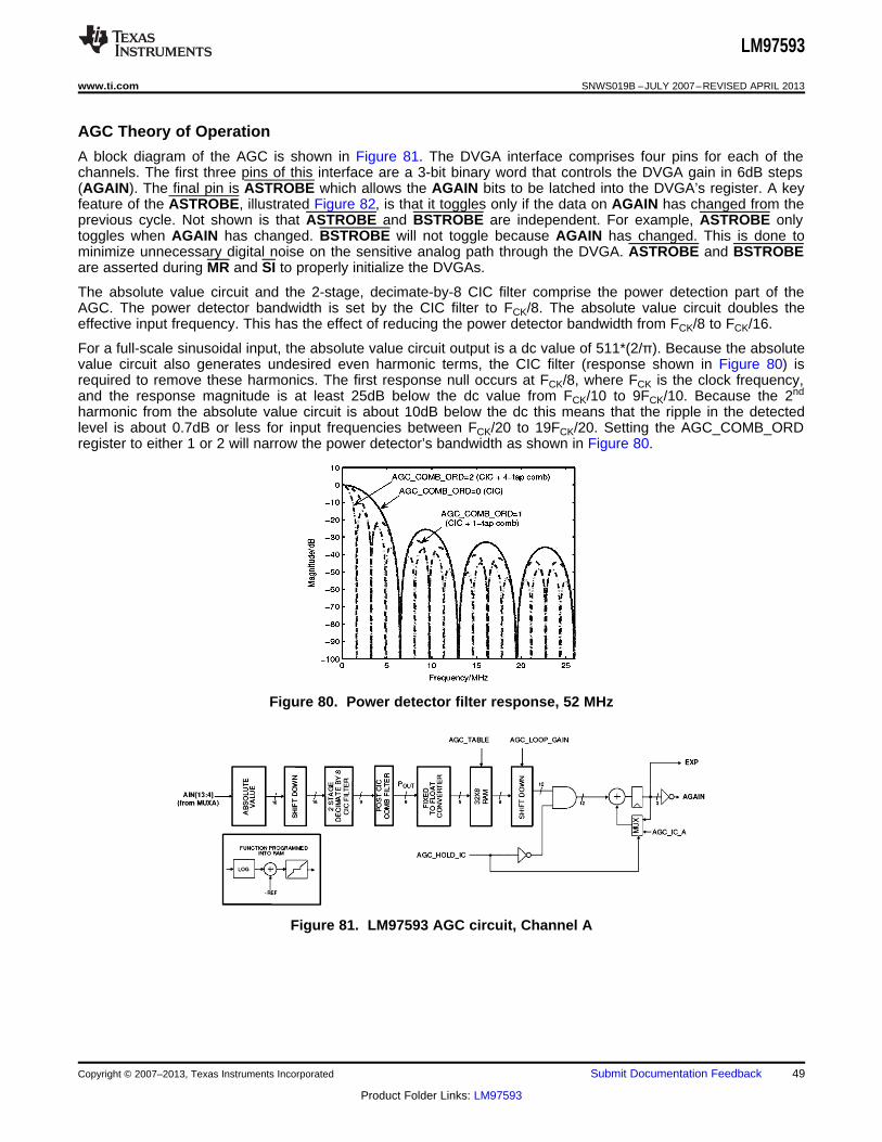
LM97593
www.ti.com SNWS019B –JULY 2007–REVISED APRIL 2013
AGC Theory of Operation
A block diagram of the AGC is shown in Figure 81. The DVGA interface comprises four pins for each of thechannels. The first three pins of this interface are a 3-bit binary word that controls the DVGA gain in 6dB steps(AGAIN). The final pin is ASTROBE which allows the AGAIN bits to be latched into the DVGA’s register. A keyfeature of the ASTROBE, illustrated Figure 82, is that it toggles only if the data on AGAIN has changed from theprevious cycle. Not shown is that ASTROBE and BSTROBE are independent. For example, ASTROBE onlytoggles when AGAIN has changed. BSTROBE will not toggle because AGAIN has changed. This is done tominimize unnecessary digital noise on the sensitive analog path through the DVGA. ASTROBE and BSTROBEare asserted during MR and SI to properly initialize the DVGAs.
The absolute value circuit and the 2-stage, decimate-by-8 CIC filter comprise the power detection part of theAGC. The power detector bandwidth is set by the CIC filter to FCK/8. The absolute value circuit doubles theeffective input frequency. This has the effect of reducing the power detector bandwidth from FCK/8 to FCK/16.
For a full-scale sinusoidal input, the absolute value circuit output is a dc value of 511*(2/π). Because the absolutevalue circuit also generates undesired even harmonic terms, the CIC filter (response shown in Figure 80) isrequired to remove these harmonics. The first response null occurs at FCK/8, where FCK is the clock frequency,and the response magnitude is at least 25dB below the dc value from FCK/10 to 9FCK/10. Because the 2nd
harmonic from the absolute value circuit is about 10dB below the dc this means that the ripple in the detectedlevel is about 0.7dB or less for input frequencies between FCK/20 to 19FCK/20. Setting the AGC_COMB_ORDregister to either 1 or 2 will narrow the power detector’s bandwidth as shown in Figure 80.
Figure 80. Power detector filter response, 52 MHz
Figure 81. LM97593 AGC circuit, Channel A
Copyright © 2007–2013, Texas Instruments Incorporated Submit Documentation Feedback 49
Product Folder Links: LM97593
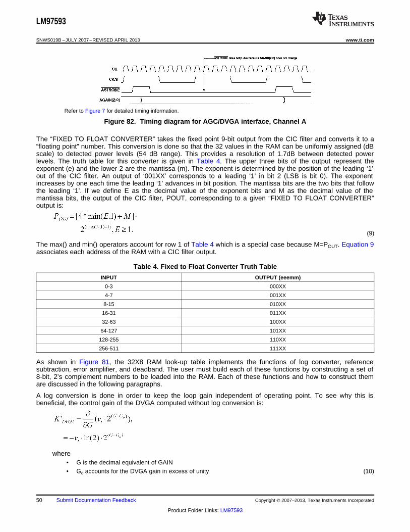
LM97593
SNWS019B –JULY 2007–REVISED APRIL 2013 www.ti.com
Refer to Figure 7 for detailed timing information.
Figure 82. Timing diagram for AGC/DVGA interface, Channel A
The “FIXED TO FLOAT CONVERTER” takes the fixed point 9-bit output from the CIC filter and converts it to a“floating point” number. This conversion is done so that the 32 values in the RAM can be uniformly assigned (dBscale) to detected power levels (54 dB range). This provides a resolution of 1.7dB between detected powerlevels. The truth table for this converter is given in Table 4. The upper three bits of the output represent theexponent (e) and the lower 2 are the mantissa (m). The exponent is determined by the position of the leading ‘1’out of the CIC filter. An output of ‘001XX’ corresponds to a leading ‘1’ in bit 2 (LSB is bit 0). The exponentincreases by one each time the leading ‘1’ advances in bit position. The mantissa bits are the two bits that followthe leading ‘1’. If we define E as the decimal value of the exponent bits and M as the decimal value of themantissa bits, the output of the CIC filter, POUT, corresponding to a given “FIXED TO FLOAT CONVERTER”output is:
(9)
The max() and min() operators account for row 1 of Table 4 which is a special case because M=POUT. Equation 9associates each address of the RAM with a CIC filter output.
Table 4. Fixed to Float Converter Truth Table
INPUT OUTPUT (eeemm)
0-3 000XX
4-7 001XX
8-15 010XX
16-31 011XX
32-63 100XX
64-127 101XX
128-255 110XX
256-511 111XX
As shown in Figure 81, the 32X8 RAM look-up table implements the functions of log converter, referencesubtraction, error amplifier, and deadband. The user must build each of these functions by constructing a set of8-bit, 2’s complement numbers to be loaded into the RAM. Each of these functions and how to construct themare discussed in the following paragraphs.
A log conversion is done in order to keep the loop gain independent of operating point. To see why this isbeneficial, the control gain of the DVGA computed without log conversion is:
where• G is the decimal equivalent of GAIN• Go accounts for the DVGA gain in excess of unity (10)
50 Submit Documentation Feedback Copyright © 2007–2013, Texas Instruments Incorporated
Product Folder Links: LM97593
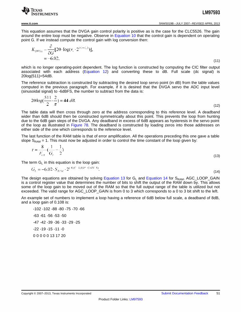
LM97593
www.ti.com SNWS019B –JULY 2007–REVISED APRIL 2013
This equation assumes that the DVGA gain control polarity is positive as is the case for the CLC5526. The gainaround the entire loop must be negative. Observe in Equation 10 that the control gain is dependent on operatingpoint G. If we instead compute the control gain with log conversion then:
(11)
which is no longer operating-point dependent. The log function is constructed by computing the CIC filter outputassociated with each address (Equation 12) and converting these to dB. Full scale (dc signal) is20log(511)=54dB.
The reference subtraction is constructed by subtracting the desired loop servo point (in dB) from the table valuescomputed in the previous paragraph. For example, if it is desired that the DVGA servo the ADC input level(sinusoidal signal) to -6dBFS, the number to subtract from the data is:
(12)
The table data will then cross through zero at the address corresponding to this reference level. A deadbandwider than 6dB should then be constructed symmetrically about this point. This prevents the loop from huntingdue to the 6dB gain steps of the DVGA. Any deadband in excess of 6dB appears as hysteresis in the servo pointof the loop as illustrated in Figure 78. The deadband is constructed by loading zeros into those addresses oneither side of the one which corresponds to the reference level.
The last function of the RAM table is that of error amplification. All the operations preceding this one gave a tableslope SRAM = 1. This must now be adjusted in order to control the time constant of the loop given by:
(13)
The term GL in this equation is the loop gain:
(14)
The design equations are obtained by solving Equation 13 for GL and Equation 14 for SRAM. AGC_LOOP_GAINis a control register value that determines the number of bits to shift the output of the RAM down by. This allowssome of the loop gain to be moved out of the RAM so that the full output range of the table is utilized but notexceeded. The valid range for AGC_LOOP_GAIN is from 0 to 3 which corresponds to a 0 to 3 bit shift to the left.
An example set of numbers to implement a loop having a reference of 6dB below full scale, a deadband of 8dB,and a loop gain of 0.108 is:
-102 -102 -88 -80 -75 -70 -66
-63 -61 -56 -53 -50
-47 -42 -39 -36 -33 -29 -25
-22 -19 -15 -11 -0
0 0 0 0 0 13 17 20
Copyright © 2007–2013, Texas Instruments Incorporated Submit Documentation Feedback 51
Product Folder Links: LM97593
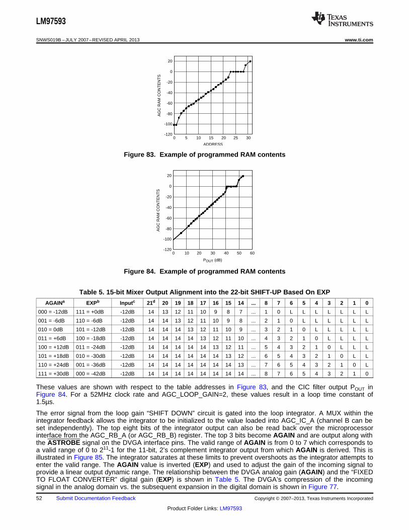
0 60
POUT (dB)
-120
-100
-80
-60
-40
0
20
AG
C R
AM
CO
NT
EN
TS
5040302010
-20
0 30
ADDRESS
-120
-100
-80
-60
-40
0
20
AG
C R
AM
CO
NT
EN
TS
252015105
-20
LM97593
SNWS019B –JULY 2007–REVISED APRIL 2013 www.ti.com
Figure 83. Example of programmed RAM contents
Figure 84. Example of programmed RAM contents
Table 5. 15-bit Mixer Output Alignment into the 22-bit SHIFT-UP Based On EXP
AGAINa EXPb Inputc 21d 20 19 18 17 16 15 14 ... 8 7 6 5 4 3 2 1 0
000 = -12dB 111 = +0dB -12dB 14 13 12 11 10 9 8 7 ... 1 0 L L L L L L L
001 = -6dB 110 = -6dB -12dB 14 14 13 12 11 10 9 8 ... 2 1 0 L L L L L L
010 = 0dB 101 = -12dB -12dB 14 14 14 13 12 11 10 9 ... 3 2 1 0 L L L L L
011 = +6dB 100 = -18dB -12dB 14 14 14 14 13 12 11 10 ... 4 3 2 1 0 L L L L
100 = +12dB 011 = -24dB -12dB 14 14 14 14 14 13 12 11 ... 5 4 3 2 1 0 L L L
101 = +18dB 010 = -30dB -12dB 14 14 14 14 14 14 13 12 ... 6 5 4 3 2 1 0 L L
110 = +24dB 001 = -36dB -12dB 14 14 14 14 14 14 14 13 ... 7 6 5 4 3 2 1 0 L
111 = +30dB 000 = -42dB -12dB 14 14 14 14 14 14 14 14 ... 8 7 6 5 4 3 2 1 0
These values are shown with respect to the table addresses in Figure 83, and the CIC filter output POUT inFigure 84. For a 52MHz clock rate and AGC_LOOP_GAIN=2, these values result in a loop time constant of1.5µs.
The error signal from the loop gain “SHIFT DOWN” circuit is gated into the loop integrator. A MUX within theintegrator feedback allows the integrator to be initialized to the value loaded into AGC_IC_A (channel B can beset independently). The top eight bits of the integrator output can also be read back over the microprocessorinterface from the AGC_RB_A (or AGC_RB_B) register. The top 3 bits become AGAIN and are output along withthe ASTROBE signal on the DVGA interface pins. The valid range of AGAIN is from 0 to 7 which corresponds toa valid range of 0 to 211-1 for the 11-bit, 2’s complement integrator output from which AGAIN is derived. This isillustrated in Figure 85. The integrator saturates at these limits to prevent overshoots as the integrator attempts toenter the valid range. The AGAIN value is inverted (EXP) and used to adjust the gain of the incoming signal toprovide a linear output dynamic range. The relationship between the DVGA analog gain (AGAIN) and the “FIXEDTO FLOAT CONVERTER” digital gain (EXP) is shown in Table 5. The DVGA’s compression of the incomingsignal in the analog domain vs. the subsequent expansion in the digital domain is shown in Figure 77.
52 Submit Documentation Feedback Copyright © 2007–2013, Texas Instruments Incorporated
Product Folder Links: LM97593
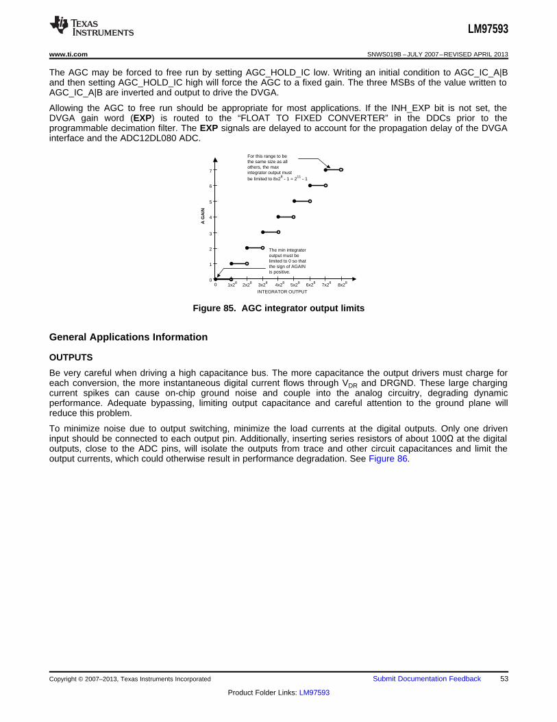
3x282x281x2800
4x28 5x28 6x287x28 8x28
INTEGRATOR OUTPUT
The min integratoroutput must belimited to 0 so thatthe sign of AGAINis positive.
A G
AIN
1
2
3
4
5
6
7
For this range to bethe same size as allothers, the maxintegrator output mustbe limited to 8x28 - 1 = 211 - 1
LM97593
www.ti.com SNWS019B –JULY 2007–REVISED APRIL 2013
The AGC may be forced to free run by setting AGC_HOLD_IC low. Writing an initial condition to AGC_IC_A|Band then setting AGC_HOLD_IC high will force the AGC to a fixed gain. The three MSBs of the value written toAGC_IC_A|B are inverted and output to drive the DVGA.
Allowing the AGC to free run should be appropriate for most applications. If the INH_EXP bit is not set, theDVGA gain word (EXP) is routed to the “FLOAT TO FIXED CONVERTER” in the DDCs prior to theprogrammable decimation filter. The EXP signals are delayed to account for the propagation delay of the DVGAinterface and the ADC12DL080 ADC.
Figure 85. AGC integrator output limits
General Applications Information
OUTPUTS
Be very careful when driving a high capacitance bus. The more capacitance the output drivers must charge foreach conversion, the more instantaneous digital current flows through VDR and DRGND. These large chargingcurrent spikes can cause on-chip ground noise and couple into the analog circuitry, degrading dynamicperformance. Adequate bypassing, limiting output capacitance and careful attention to the ground plane willreduce this problem.
To minimize noise due to output switching, minimize the load currents at the digital outputs. Only one driveninput should be connected to each output pin. Additionally, inserting series resistors of about 100Ω at the digitaloutputs, close to the ADC pins, will isolate the outputs from trace and other circuit capacitances and limit theoutput currents, which could otherwise result in performance degradation. See Figure 86.
Copyright © 2007–2013, Texas Instruments Incorporated Submit Documentation Feedback 53
Product Folder Links: LM97593
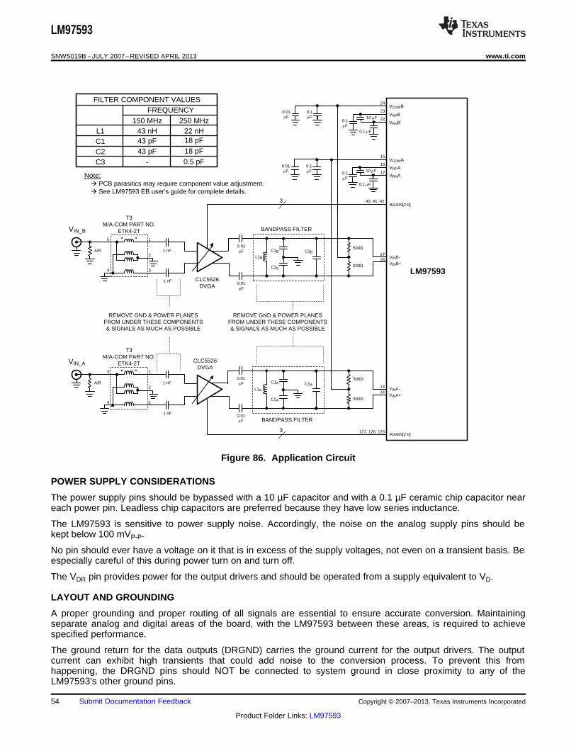
LM97593
VINA-
VINA+
1314
24
23
22
VINB-
VINB+
15
16
17
0.1 PF
0.1PF
10 PF
0.1 PF
0.1PF
10 PF
0.1PF
REMOVE GND & POWER PLANES FROM UNDER THESE COMPONENTS & SIGNALS AS MUCH AS POSSIBLE
VCOMB
VRPB
VRNB
VCOMA
VRPA
VRNA
VIN_A
0.01PF
T3M/A-COM PART NO.
ETK4-2T CLC5526DVGA
1
2
34
5
1 nF
1 nF
0.01PF
0.01PF
L1A
C1A
C2A
C3A
500Ö
500Ö
REMOVE GND & POWER PLANES FROM UNDER THESE COMPONENTS & SIGNALS AS MUCH AS POSSIBLE
2726
VIN_B
T3M/A-COM PART NO.
ETK4-2T
CLC5526DVGA
1
2
34
5
1 nF
1 nF
0.01PF
0.01PF
L1B
C1B
C2B
C3B500Ö
500Ö
BANDPASS FILTER
0.1PF
0.01PF
BANDPASS FILTER
AGAIN[2:0]3
BGAIN[2:0]3 40, 41, 42
127, 126, 125
Note:Æ PCB parasitics may require component value adjustment.Æ See LM97593 (%XVHU¶VJXLGHIRUFRPSOHWHGHWDLOV.
A/R
A/R
150 MHz 250 MHzL1 43 nH 22 nHC1 43 pF 18 pF
C2 43 pF 18 pF
C3 - 0.5 pF
FILTER COMPONENT VALUESFREQUENCY
LM97593
SNWS019B –JULY 2007–REVISED APRIL 2013 www.ti.com
Figure 86. Application Circuit
POWER SUPPLY CONSIDERATIONS
The power supply pins should be bypassed with a 10 µF capacitor and with a 0.1 µF ceramic chip capacitor neareach power pin. Leadless chip capacitors are preferred because they have low series inductance.
The LM97593 is sensitive to power supply noise. Accordingly, the noise on the analog supply pins should bekept below 100 mVP-P.
No pin should ever have a voltage on it that is in excess of the supply voltages, not even on a transient basis. Beespecially careful of this during power turn on and turn off.
The VDR pin provides power for the output drivers and should be operated from a supply equivalent to VD.
LAYOUT AND GROUNDING
A proper grounding and proper routing of all signals are essential to ensure accurate conversion. Maintainingseparate analog and digital areas of the board, with the LM97593 between these areas, is required to achievespecified performance.
The ground return for the data outputs (DRGND) carries the ground current for the output drivers. The outputcurrent can exhibit high transients that could add noise to the conversion process. To prevent this fromhappening, the DRGND pins should NOT be connected to system ground in close proximity to any of theLM97593's other ground pins.
54 Submit Documentation Feedback Copyright © 2007–2013, Texas Instruments Incorporated
Product Folder Links: LM97593
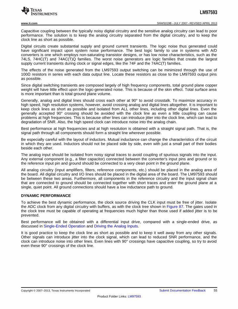
LM97593
www.ti.com SNWS019B –JULY 2007–REVISED APRIL 2013
Capacitive coupling between the typically noisy digital circuitry and the sensitive analog circuitry can lead to poorperformance. The solution is to keep the analog circuitry separated from the digital circuitry, and to keep theclock line as short as possible.
Digital circuits create substantial supply and ground current transients. The logic noise thus generated couldhave significant impact upon system noise performance. The best logic family to use in systems with A/Dconverters is one which employs non-saturating transistor designs, or has low noise characteristics, such as the74LS, 74HC(T) and 74AC(T)Q families. The worst noise generators are logic families that create the largestsupply current transients during clock or signal edges, like the 74F and the 74AC(T) families.
The effects of the noise generated from the LM97593 output switching can be minimized through the use of100Ω resistors in series with each data output line. Locate these resistors as close to the LM97593 output pinsas possible.
Since digital switching transients are composed largely of high frequency components, total ground plane copperweight will have little effect upon the logic-generated noise. This is because of the skin effect. Total surface areais more important than is total ground plane volume.
Generally, analog and digital lines should cross each other at 90° to avoid crosstalk. To maximize accuracy inhigh speed, high resolution systems, however, avoid crossing analog and digital lines altogether. It is important tokeep clock lines as short as possible and isolated from ALL other lines, including other digital lines. Even thegenerally accepted 90° crossing should be avoided with the clock line as even a little coupling can causeproblems at high frequencies. This is because other lines can introduce jitter into the clock line, which can lead todegradation of SNR. Also, the high speed clock can introduce noise into the analog chain.
Best performance at high frequencies and at high resolution is obtained with a straight signal path. That is, thesignal path through all components should form a straight line wherever possible.
Be especially careful with the layout of inductors. Mutual inductance can change the characteristics of the circuitin which they are used. Inductors should not be placed side by side, even with just a small part of their bodiesbeside each other.
The analog input should be isolated from noisy signal traces to avoid coupling of spurious signals into the input.Any external component (e.g., a filter capacitor) connected between the converter's input pins and ground or tothe reference input pin and ground should be connected to a very clean point in the ground plane.
All analog circuitry (input amplifiers, filters, reference components, etc.) should be placed in the analog area ofthe board. All digital circuitry and I/O lines should be placed in the digital area of the board. The LM97593 shouldbe between these two areas. Furthermore, all components in the reference circuitry and the input signal chainthat are connected to ground should be connected together with short traces and enter the ground plane at asingle, quiet point. All ground connections should have a low inductance path to ground.
DYNAMIC PERFORMANCE
To achieve the best dynamic performance, the clock source driving the CLK input must be free of jitter. Isolatethe ADC clock from any digital circuitry with buffers, as with the clock tree shown in Figure 87. The gates used inthe clock tree must be capable of operating at frequencies much higher than those used if added jitter is to beprevented.
Best performance will be obtained with a differential input drive, compared with a single-ended drive, asdiscussed in Single-Ended Operation and Driving the Analog Inputs.
It is good practice to keep the clock line as short as possible and to keep it well away from any other signals.Other signals can introduce jitter into the clock signal, which can lead to reduced SNR performance, and theclock can introduce noise into other lines. Even lines with 90° crossings have capacitive coupling, so try to avoideven these 90° crossings of the clock line.
Copyright © 2007–2013, Texas Instruments Incorporated Submit Documentation Feedback 55
Product Folder Links: LM97593
LM97593
SNWS019B –JULY 2007–REVISED APRIL 2013 www.ti.com
Figure 87. Isolating the ADC Clock from other Circuitry with a Clock Tree
Common Application Pitfalls
Driving the inputs (analog or digital) beyond the power supply rails. For proper operation, all inputs shouldnot go more than 100 mV beyond the supply rails (more than 100 mV below the ground pins or 100 mV abovethe supply pins). Exceeding these limits on even a transient basis may cause faulty or erratic operation. It is notuncommon for high speed digital components (e.g., 74F and 74AC devices) to exhibit overshoot or undershootthat goes above the power supply or below ground. A resistor of about 47Ω to 100Ω in series with any offendingdigital input, close to the signal source, will eliminate the problem.
Do not allow input voltages to exceed the supply voltage, even on a transient basis. Not even during power up orpower down.
Be careful not to overdrive the inputs of the LM97593 with a device that is powered from supplies outside therange of the LM97593 supply. Such practice may lead to conversion inaccuracies and even to device damage.
Attempting to drive a high capacitance digital data bus. The more capacitance the output drivers mustcharge for each conversion, the more instantaneous digital current flows through VDR and DRGND. These largecharging current spikes can couple into the analog circuitry, degrading dynamic performance. Adequatebypassing and maintaining separate analog and digital areas on the pc board will reduce this problem.
The digital data outputs should be buffered (with 74ACQ541, for example) if they will drive a large capacitiveload. Dynamic performance can also be improved by adding series resistors at each digital output, close to theLM97593, which reduces the energy coupled back into the part's output pins by limiting the output current. Areasonable value for these resistors is 100Ω.
Using an inadequate amplifier to drive the analog input. As explained in Signal Inputs, the capacitance seenat the input alternates between 8 pF and 7 pF, depending upon the phase of the clock. This dynamic load ismore difficult to drive than is a fixed capacitance. If the amplifier exhibits overshoot, ringing, or any evidence ofinstability, even at a very low level, it will degrade performance. A small series resistor at each amplifier outputand a capacitor at the analog inputs will improve performance.
Also, it is important that the signals at the two inputs have exactly the same amplitude and be exactly 180º out ofphase with each other. Board layout, especially equality of the length of the two traces to the input pins, willaffect the effective phase between these two signals. Remember that an operational amplifier operated in thenon-inverting configuration will exhibit more time delay than will the same device operating in the invertingconfiguration.
Operating with the reference pins outside of the specified range. As mentioned in Reference Pins, VREFshould be in the range of
0.8V ≤ VREF ≤ 1.2V (15)
Operating outside of these limits could lead to performance degradation.
Inadequate network on Reference Bypass pins (VRPA, VRNA, VCOMA, VRPB, VRNB and VCOMB). As mentionedin Reference Pins, these pins should be bypassed with 0.1 µF capacitors to ground at VRMA and VRMB and witha 10 µF between pins VRPA and VRNA and between VRPB and VRNB for best performance.
Using a clock source with excessive jitter, using excessively long clock signal trace, or having othersignals coupled to the clock signal trace. This will cause the sampling interval to vary, causing excessiveoutput noise and a reduction in SNR and SINAD performance.
56 Submit Documentation Feedback Copyright © 2007–2013, Texas Instruments Incorporated
Product Folder Links: LM97593
LM97593
www.ti.com SNWS019B –JULY 2007–REVISED APRIL 2013
Evaluation Hardware
Evaluation boards are available to facilitate designs based on the LM97593:
LM97593EB
The LM97593 evaluation board provides a complete narrowband receiver from IF to digital symbols.
SOFTWARE
Control panel software for the LM97593 supports complete device configuration on both evaluation boards.
Integrated capture software manages the capture of data and its storage in a file on a PC.
Matlab script files support data analysis: FFT, DNL, and INL plotting.
This software and additional application information is available on the Basestation CDROM.
Copyright © 2007–2013, Texas Instruments Incorporated Submit Documentation Feedback 57
Product Folder Links: LM97593
LM97593
SNWS019B –JULY 2007–REVISED APRIL 2013 www.ti.com
REVISION HISTORY
Changes from Revision A (April 2013) to Revision B Page
• Changed layout of National Data Sheet to TI format .......................................................................................................... 57
58 Submit Documentation Feedback Copyright © 2007–2013, Texas Instruments Incorporated
Product Folder Links: LM97593
PACKAGE OPTION ADDENDUM
www.ti.com 4-Apr-2014
Addendum-Page 1
PACKAGING INFORMATION
Orderable Device Status(1)
Package Type PackageDrawing
Pins PackageQty
Eco Plan(2)
Lead/Ball Finish(6)
MSL Peak Temp(3)
Op Temp (°C) Device Marking(4/5)
Samples
LM97593VH/NOPB ACTIVE QFP NND 128 66 Green (RoHS& no Sb/Br)
CU SN Level-3-245C-168 HR -40 to 85 LM97593VH
(1) The marketing status values are defined as follows:ACTIVE: Product device recommended for new designs.LIFEBUY: TI has announced that the device will be discontinued, and a lifetime-buy period is in effect.NRND: Not recommended for new designs. Device is in production to support existing customers, but TI does not recommend using this part in a new design.PREVIEW: Device has been announced but is not in production. Samples may or may not be available.OBSOLETE: TI has discontinued the production of the device.
(2) Eco Plan - The planned eco-friendly classification: Pb-Free (RoHS), Pb-Free (RoHS Exempt), or Green (RoHS & no Sb/Br) - please check http://www.ti.com/productcontent for the latest availabilityinformation and additional product content details.TBD: The Pb-Free/Green conversion plan has not been defined.Pb-Free (RoHS): TI's terms "Lead-Free" or "Pb-Free" mean semiconductor products that are compatible with the current RoHS requirements for all 6 substances, including the requirement thatlead not exceed 0.1% by weight in homogeneous materials. Where designed to be soldered at high temperatures, TI Pb-Free products are suitable for use in specified lead-free processes.Pb-Free (RoHS Exempt): This component has a RoHS exemption for either 1) lead-based flip-chip solder bumps used between the die and package, or 2) lead-based die adhesive used betweenthe die and leadframe. The component is otherwise considered Pb-Free (RoHS compatible) as defined above.Green (RoHS & no Sb/Br): TI defines "Green" to mean Pb-Free (RoHS compatible), and free of Bromine (Br) and Antimony (Sb) based flame retardants (Br or Sb do not exceed 0.1% by weightin homogeneous material)
(3) MSL, Peak Temp. - The Moisture Sensitivity Level rating according to the JEDEC industry standard classifications, and peak solder temperature.
(4) There may be additional marking, which relates to the logo, the lot trace code information, or the environmental category on the device.
(5) Multiple Device Markings will be inside parentheses. Only one Device Marking contained in parentheses and separated by a "~" will appear on a device. If a line is indented then it is a continuationof the previous line and the two combined represent the entire Device Marking for that device.
(6) Lead/Ball Finish - Orderable Devices may have multiple material finish options. Finish options are separated by a vertical ruled line. Lead/Ball Finish values may wrap to two lines if the finishvalue exceeds the maximum column width.
Important Information and Disclaimer:The information provided on this page represents TI's knowledge and belief as of the date that it is provided. TI bases its knowledge and belief on informationprovided by third parties, and makes no representation or warranty as to the accuracy of such information. Efforts are underway to better integrate information from third parties. TI has taken andcontinues to take reasonable steps to provide representative and accurate information but may not have conducted destructive testing or chemical analysis on incoming materials and chemicals.TI and TI suppliers consider certain information to be proprietary, and thus CAS numbers and other limited information may not be available for release.
In no event shall TI's liability arising out of such information exceed the total purchase price of the TI part(s) at issue in this document sold by TI to Customer on an annual basis.
PACKAGE OPTION ADDENDUM
www.ti.com 4-Apr-2014
Addendum-Page 2
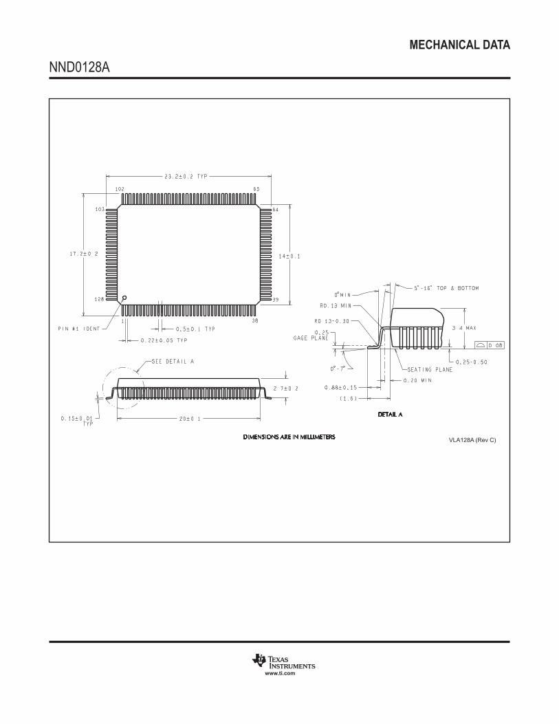
MECHANICAL DATA
NND0128A
www.ti.com
VLA128A (Rev C)

IMPORTANT NOTICETexas Instruments Incorporated and its subsidiaries (TI) reserve the right to make corrections, enhancements, improvements and otherchanges to its semiconductor products and services per JESD46, latest issue, and to discontinue any product or service per JESD48, latestissue. Buyers should obtain the latest relevant information before placing orders and should verify that such information is current andcomplete. All semiconductor products (also referred to herein as “components”) are sold subject to TI’s terms and conditions of salesupplied at the time of order acknowledgment.TI warrants performance of its components to the specifications applicable at the time of sale, in accordance with the warranty in TI’s termsand conditions of sale of semiconductor products. Testing and other quality control techniques are used to the extent TI deems necessaryto support this warranty. Except where mandated by applicable law, testing of all parameters of each component is not necessarilyperformed.TI assumes no liability for applications assistance or the design of Buyers’ products. Buyers are responsible for their products andapplications using TI components. To minimize the risks associated with Buyers’ products and applications, Buyers should provideadequate design and operating safeguards.TI does not warrant or represent that any license, either express or implied, is granted under any patent right, copyright, mask work right, orother intellectual property right relating to any combination, machine, or process in which TI components or services are used. Informationpublished by TI regarding third-party products or services does not constitute a license to use such products or services or a warranty orendorsement thereof. Use of such information may require a license from a third party under the patents or other intellectual property of thethird party, or a license from TI under the patents or other intellectual property of TI.Reproduction of significant portions of TI information in TI data books or data sheets is permissible only if reproduction is without alterationand is accompanied by all associated warranties, conditions, limitations, and notices. TI is not responsible or liable for such altereddocumentation. Information of third parties may be subject to additional restrictions.Resale of TI components or services with statements different from or beyond the parameters stated by TI for that component or servicevoids all express and any implied warranties for the associated TI component or service and is an unfair and deceptive business practice.TI is not responsible or liable for any such statements.Buyer acknowledges and agrees that it is solely responsible for compliance with all legal, regulatory and safety-related requirementsconcerning its products, and any use of TI components in its applications, notwithstanding any applications-related information or supportthat may be provided by TI. Buyer represents and agrees that it has all the necessary expertise to create and implement safeguards whichanticipate dangerous consequences of failures, monitor failures and their consequences, lessen the likelihood of failures that might causeharm and take appropriate remedial actions. Buyer will fully indemnify TI and its representatives against any damages arising out of the useof any TI components in safety-critical applications.In some cases, TI components may be promoted specifically to facilitate safety-related applications. With such components, TI’s goal is tohelp enable customers to design and create their own end-product solutions that meet applicable functional safety standards andrequirements. Nonetheless, such components are subject to these terms.No TI components are authorized for use in FDA Class III (or similar life-critical medical equipment) unless authorized officers of the partieshave executed a special agreement specifically governing such use.Only those TI components which TI has specifically designated as military grade or “enhanced plastic” are designed and intended for use inmilitary/aerospace applications or environments. Buyer acknowledges and agrees that any military or aerospace use of TI componentswhich have not been so designated is solely at the Buyer's risk, and that Buyer is solely responsible for compliance with all legal andregulatory requirements in connection with such use.TI has specifically designated certain components as meeting ISO/TS16949 requirements, mainly for automotive use. In any case of use ofnon-designated products, TI will not be responsible for any failure to meet ISO/TS16949.Products ApplicationsAudio www.ti.com/audio Automotive and Transportation www.ti.com/automotiveAmplifiers amplifier.ti.com Communications and Telecom www.ti.com/communicationsData Converters dataconverter.ti.com Computers and Peripherals www.ti.com/computersDLP® Products www.dlp.com Consumer Electronics www.ti.com/consumer-appsDSP dsp.ti.com Energy and Lighting www.ti.com/energyClocks and Timers www.ti.com/clocks Industrial www.ti.com/industrialInterface interface.ti.com Medical www.ti.com/medicalLogic logic.ti.com Security www.ti.com/securityPower Mgmt power.ti.com Space, Avionics and Defense www.ti.com/space-avionics-defenseMicrocontrollers microcontroller.ti.com Video and Imaging www.ti.com/videoRFID www.ti-rfid.comOMAP Applications Processors www.ti.com/omap TI E2E Community e2e.ti.comWireless Connectivity www.ti.com/wirelessconnectivity
Mailing Address: Texas Instruments, Post Office Box 655303, Dallas, Texas 75265Copyright © 2014, Texas Instruments Incorporated