lm5026 active clamp current mode pwm controller (rev. d)
TRANSCRIPT

T1
CS
VIN36 - 78V
VOUT3.3V
SYNC I/O
LM5026
UVLO
PGND AGND
COMP
OUT_A
OUT_B
VCC
SS
RT
SYNC
REF
TIMERES
CSVIN
DCL
ERRORAMP and
ISOLATION
Product
Folder
Sample &Buy
Technical
Documents
Tools &
Software
Support &Community
ReferenceDesign
LM5026SNVS363E –AUGUST 2005–REVISED NOVEMBER 2015
LM5026 Active Clamp Current Mode PWM Controller1 Features 3 Description
The LM5026 PWM controller contains all of the1• Current-Mode Control
features necessary to implement power converters• Internal 100-V Start-Up Bias Regulator utilizing the active clamp and reset technique with• 3-A Compound Main Gate Driver current-mode control. With the active clamp
technique, higher efficiencies and greater power• High Bandwidth Optocoupler Interfacedensities can be realized compared to conventional• Programmable Line Undervoltage Lockout (UVLO) catch winding or RDC clamp and reset techniques.With Adjustable Hysteresis Two control outputs are provided, the main power
• Versatile Dual Mode Overcurrent Protection With switch control (OUT_A) and the active clamp switchHiccup Delay Timer control (OUT_B). The device can be configured to
control either a P-Channel or N-Channel clamp• Programmable Overlap or Deadtime between theswitch. The main gate driver features a compoundMain and Active Clamp Outputsconfiguration, consisting of both MOS and Bipolar• Programmable Maximum Duty Cycle Clamp devices, providing superior gate drive characteristics.
• Programmable Soft-Start The LM5026 can be configured to operate with biasvoltages over a wide input range of 8 V to 100 V.• Leading Edge BlankingAdditional features include programmable maximum• Resistor Programmed 1-MHz Capable Oscillator duty cycle, line undervoltage lockout, cycle-by-cycle
• Oscillator Sync I/O Capability current limit, hiccup mode fault operation withadjustable timeout delay, PWM slope compensation,• Precision 5-V Referencesoft-start, 1-MHz capable oscillator withsynchronization input and output capability, precision2 Applicationsreference, and thermal shutdown.
• Server Power Supplies• 48-V Telecom Power Supplies Device Information(1)
PART NUMBER PACKAGE BODY SIZE (NOM)• High Efficiency DC–DC Power SuppliesWSON (16) 5.00 mm × 5.00 mm
LM5026TSSOP (16) 4.40 mm × 5.00 mm
(1) For all available packages, see the orderable addendum atthe end of the data sheet.
Typical Application Circuit
1
An IMPORTANT NOTICE at the end of this data sheet addresses availability, warranty, changes, use in safety-critical applications,intellectual property matters and other important disclaimers. PRODUCTION DATA.

LM5026SNVS363E –AUGUST 2005–REVISED NOVEMBER 2015 www.ti.com
Table of Contents7.3 Feature Description................................................. 121 Features .................................................................. 17.4 Device Functional Modes........................................ 192 Applications ........................................................... 1
8 Application and Implementation ........................ 203 Description ............................................................. 18.1 Application Information............................................ 204 Revision History..................................................... 28.2 Typical Application ................................................. 255 Pin Configuration and Functions ......................... 3
9 Power Supply Recommendations ...................... 296 Specifications......................................................... 410 Layout................................................................... 296.1 Absolute Maximum Ratings ...................................... 4
10.1 Layout Guidelines ................................................. 296.2 ESD Ratings.............................................................. 410.2 Layout Example .................................................... 306.3 Recommended Operating Conditions....................... 4
11 Device and Documentation Support ................. 316.4 Thermal Information .................................................. 511.1 Community Resources.......................................... 316.5 Electrical Characteristics........................................... 511.2 Trademarks ........................................................... 316.6 Typical Characteristics .............................................. 811.3 Electrostatic Discharge Caution............................ 317 Detailed Description ............................................ 1111.4 Glossary ................................................................ 317.1 Overview ................................................................. 11
12 Mechanical, Packaging, and Orderable7.2 Functional Block Diagram ....................................... 11Information ........................................................... 31
4 Revision HistoryNOTE: Page numbers for previous revisions may differ from page numbers in the current version.
Changes from Revision D (April 2013) to Revision E Page
• Added ESD Ratings table, Feature Description section, Device Functional Modes, Application and Implementationsection, Power Supply Recommendations section, Layout section, Device and Documentation Support section, andMechanical, Packaging, and Orderable Information section. ................................................................................................ 1
Changes from Revision C (April 2013) to Revision D Page
• Changed layout of National Data Sheet to TI format ........................................................................................................... 25
2 Submit Documentation Feedback Copyright © 2005–2015, Texas Instruments Incorporated
Product Folder Links: LM5026

UVLO
CS
RES
TIME
REF
VCC
OUT_A
VIN
RT
COMP
SS
AGND
PGND
OUT_B
SYNC
DCL
14
13
12
11
10
8
15
161
2
3
4
5
7
6
9
VIN
VCC
RES
REF
CS
UVLO
OUT_A
TIME
1
2
3
4
5
6
7
8 9
10
11
1213
14
15
16
SYNC
COMP
DCL
PGND
RT
SS
OUT_B
AGND
EP
LM5026www.ti.com SNVS363E –AUGUST 2005–REVISED NOVEMBER 2015
5 Pin Configuration and Functions
PW Package NHQ Package16-Pin TSSOP 16-Pin WSON
Top View Top View
Pin FunctionsPIN
TYPE (1) DESCRIPTIONNO. NAME
Input voltage source. Input to the start-up regulator. Operating input range is 13 V to 100 V1 VIN I with transient capability to 105 V. For power sources outside of this range, the LM5026 can
be biased directly at VCC by an external regulator.Line undervoltage lockout. An external voltage divider from the power source sets theshutdown and standby comparator levels. When UVLO reaches the 0.4-V threshold the VCC2 UVLO I and REF regulators are enabled. At the 1.25-V threshold the SS pin is released and thedevice enters the active mode.Current Sense input for current mode control and current limit. If CS exceeds 0.5 V, the
3 CS I output pulse will be terminated, entering cycle-by-cycle current limit. An internal switch holdsCS low for 100 nS after OUT_A switches high to blank leading edge transients.Restart Timer. If cycle-by-cycle current limit is reached during any cycle, a 10-µA current issourced to the RES pin capacitor. If the RES capacitor voltage reaches 2.5 V, the soft-start
4 RES I capacitor will be fully discharged and then released with a pullup current of 1 µA. After thefirst output pulse at OUT_A (when SS = 1.4 V), the SS pin charging current will revert backto 50 µA.Gate drive overlap or deadtime control. An external resistor (RSET) sets either the overlaptime or deadtime for the active clamp output. An RSET resistor connected between TIME
5 TIME I and AGND produces in-phase OUT_A and OUT_B pulses with overlap. An RSET resistorconnected between TIME and REF produces out-of-phase OUT_A and OUT_B pulses withdeadtime.Output of 5-V reference. Maximum output current is 10 mA. Locally decouple with a 0.1-µF6 REF O capacitor.Output of the high voltage start-up regulator. The VCC voltage is regulated to 7.6 V. If an
7 VCC P auxiliary winding raises the voltage on this pin above the regulation setpoint, the internalstart-up regulator will shutdown, thus reducing the IC power dissipation.Main output driver. Output of the main switch PWM gate driver. Capable of 3-A peak sink8 OUT_A O current.Active clamp output driver. Output of the active clamp switch gate driver. Capable of 0.5-A9 OUT_B O peak source and sink current.
10 PGND G Power ground. Connect directly to analog cround.11 AGND G Analog return. Connect directly to power cround.
Soft-start. An external capacitor and an internal 50-µA current source set the soft-start ramp.12 SS I The SS current source is reduced to 1 µA following a restart event. The soft-stop discharge
current is 50 µA.Input to the pulse width modulator. The external optocoupler connected to the COMP pinsources current into an internal NPN current mirror. The PWM duty cycle is maximum with13 COMP I zero input current, while 1 mA reduces the duty cycle to zero. The current mirror improvesthe frequency response by reducing the ac voltage across the optocoupler detector.
(1) P = Power, G = Ground, I = Input, O = Output, I/O = Input/Output
Copyright © 2005–2015, Texas Instruments Incorporated Submit Documentation Feedback 3
Product Folder Links: LM5026

LM5026SNVS363E –AUGUST 2005–REVISED NOVEMBER 2015 www.ti.com
Pin Functions (continued)PIN
TYPE (1) DESCRIPTIONNO. NAME
Oscillator frequency control. Normally biased at 2 V. The total external resistance connected14 RT I between RT and AGND sets the internal oscillator frequency.Oscillator synchronization input/output. The internal oscillator can be synchronized to an
15 SYNC I/O external clock with an external pulldown device. Multiple LM5026 devices can besynchronized together by connection of their SYNC pins.Maximum duty cycle control. An external resistor divider connected from RT to AGND sets16 DCL I the maximum output duty cycle for OUT_A.
Exposed Pad(WSON Exposed Pad, underside of WSON package. Connect to system ground plane for reducedEP GPackage thermal resistance.Only)
6 Specifications
6.1 Absolute Maximum RatingsSee (1) (2).
MIN MAX UNITVIN to GND –0.3 105 VVCC to GND –0.3 16 VCS to GND –0.3 1 VCOMP input current 10 mAAll other inputs to GND –0.3 7 VJunction temperature 150 °CStorage temperature, Tstg –65 150 °C
(1) Stresses beyond those listed under Absolute Maximum Ratings may cause permanent damage to the device. These are stress ratingsonly, which do not imply functional operation of the device at these or any other conditions beyond those indicated under RecommendedOperating Conditions. Exposure to absolute-maximum-rated conditions for extended periods may affect device reliability.
(2) If Military/Aerospace specified devices are required, please contact the TI Sales Office/ Distributors for availability and specifications.
6.2 ESD RatingsVALUE UNIT
Human body model (HBM), per ANSI/ESDA/JEDEC JS-001 (1) (2) ±2000V(ESD) Electrostatic discharge V
Charged-device model (CDM), per JEDEC specification JESD22-C101 (3) ±500
(1) JEDEC document JEP155 states that 500-V HBM allows safe manufacturing with a standard ESD control process. Manufacturing withless than 500-V HBM is possible with the necessary precautions. Pins listed as ±2000 V may actually have higher performance.
(2) The human body model is a 100-pF capacitor discharged through a 1.5-kΩ resistor into each pin.(3) JEDEC document JEP157 states that 250-V CDM allows safe manufacturing with a standard ESD control process.
6.3 Recommended Operating Conditionsover operating free-air temperature range (unless otherwise noted) (1)
MIN MAX UNITVIN voltage 13 100 VExternal voltage applied to VCC 8 15 VOperating junction temperature –40 125 °C
(1) Absolute Maximum Ratings are limits beyond which damage to the device may occur. Operating Ratings are conditions under whichoperation of the device is intended to be functional. For specifications and test conditions, see the Electrical Characteristics.
4 Submit Documentation Feedback Copyright © 2005–2015, Texas Instruments Incorporated
Product Folder Links: LM5026

LM5026www.ti.com SNVS363E –AUGUST 2005–REVISED NOVEMBER 2015
6.4 Thermal InformationLM5026
THERMAL METRIC (1) NHQ (WSON) PW (TSSOP) UNIT16 PINS 16 PINS
RθJA Junction-to-ambient thermal resistance 29.9 98.6 °C/WRθJC(top) Junction-to-case (top) thermal resistance 25.8 27.6 °C/WRθJB Junction-to-board thermal resistance 9.2 44.1 °C/WψJT Junction-to-top characterization parameter 0.2 1.2 °C/WψJB Junction-to-board characterization parameter 9.5 43.3 °C/WRθJC(bot) Junction-to-case (bottom) thermal resistance 2.3 — °C/W
(1) For more information about traditional and new thermal metrics, see the Semiconductor and IC Package Thermal Metrics applicationreport, SPRA953.
6.5 Electrical CharacteristicsSpecification typical values are for TJ = 25°C unless otherwise noted. VIN = 48 V, VCC = 10 V, RT = 30.0 kΩ, Rset = 34.8 kΩunless otherwise stated. Minimum and maximum specifications apply over full operating junction temperature range. (1)
PARAMETER TEST CONDITIONS MIN TYP MAX UNIT
START-UP REGULATOR
TJ = 25°C 7.6VCC Reg VCC regulation No Load Vover full operating junction 7.3 7.9temperature range
TJ = 25°C 25VCC current limit See (2) mAover full operating junction 20temperature range
TJ = 25°C 165Start-up regulatorI-VIN leakage (external VCC VIN = 100 V µAover full operating junction 500supply) temperature range
TJ = 25°C 350Shutdown current (Iin) UVLO = 0 V µAover full operating junction 450temperature range
VCC SUPPLY
VCC Reg –TJ = 25°CVCC undervoltage 120 mVlockout voltage V
VCC Reg – 220(positive going Vcc) over full operating junction temperature range mV
TJ = 25°C 1.5VCC undervoltage Vhysteresis over full operating junction temperature range 1 2
VCC supply current Cgate = 0, UVLO = 1.3 V, over full operating junction 4.2 mA(ICC) temperature range
REFERENCE SUPPLY
TJ = 25°C 5Ref voltage IREF = 0 mA Vover full operating junction 4.85 5.15temperature range
TJ = 25°C 25VREF Ref voltage regulation IREF = 0 to 10 mA mVover full operating junction 50temperature range
TJ = 25°C 20Ref current limit mA
over full operating junction temperature range 10
UVLO SHUTDOWN/STANDBY
TJ = 25°C 0.4Undervoltage Vshutdown threshold over full operating junction temperature range 0.3 0.5
(1) Minimum and maximum limits are 100% production tested at 25ºC. Limits over the operating temperature range are specified throughcorrelation using Statistical Quality Control (SQC) methods. Limits are used to calculate Average Outgoing Quality Level (AOQL). Allelectrical characteristics having room temperature limits are tested during production with TA = TJ = 25°C. All hot and cold limits arespecified by correlating the electrical characteristics to process and temperature variations and applying statistical process control.
(2) Device thermal limitations may limit usable range.
Copyright © 2005–2015, Texas Instruments Incorporated Submit Documentation Feedback 5
Product Folder Links: LM5026

LM5026SNVS363E –AUGUST 2005–REVISED NOVEMBER 2015 www.ti.com
Electrical Characteristics (continued)Specification typical values are for TJ = 25°C unless otherwise noted. VIN = 48 V, VCC = 10 V, RT = 30.0 kΩ, Rset = 34.8 kΩunless otherwise stated. Minimum and maximum specifications apply over full operating junction temperature range.(1)
PARAMETER TEST CONDITIONS MIN TYP MAX UNIT
Undervoltage 0.1 Vshutdown hysteresis
TJ = 25°C 1.25Undervoltage standby Vthreshold over full operating junction temperature range 1.21 1.29
Undervoltage sandby TJ = 25°C 20hysteresis current µA
over full operating junction temperature range 16 24source
CURRENT LIMIT
TJ = 25°C 0.5Cycle-by-cycle Vthreshold voltage over full operating junction temperature range 0.45 0.55
CS step from 0 to 0.6 V Time to onset of OUT transitionILIM delay-to-output 40 ns(90%) Cgate=0
TJ = 25°C 100Leading edge nsblanking time over full operating junction temperature range 70 130
TJ = 25°C 30CS sink impedance ICS = 10 mA Ωover full operating junction(clocked) 65temperature range
OVERCURRENT RESTART
TJ = 25°C 2.55Restart threshold V
over full operating junction temperature range 2.4 2.7
TJ = 25°C 10Fault-charging current µA
over full operating junction temperature range 7.5 12.5
TJ = 25°C 10Discharging current µA
over full operating junction temperature range 7.5 12.5
SOFT-START
TJ = 25°C 50Soft-start currentsource over full operating junction temperature range 38 58
TJ = 25°C 50Soft-stop current sink µAover full operating junction temperature range 38 58
Soft-start current TJ = 25°C 1source following a
over full operating junction temperature range 0.6 1.3restart event
OSCILLATOR
TJ = 25°C 200Frequency1 RT = 30 kΩ kHzover full operating junction 180 220temperature range
TJ = 25°C 590Frequency2 RT = 10 kΩ kHzover full operating junction 520 660temperature range
SYNC source current 200 µA
SYNC sink Can sync up to 5 like controllers minimum 100 Ωimpedance
Sync threshold 1.4 V(falling)
Sync pulse width over full operating junction temperature range 15 nsminimum
PWM COMPARATOR
Delay-to-output CS stepped, time to onset of OUT_A transition low 40 ns
Mimimum duty cycle ICOMP = 1 mA, over full operating junction temperature range 0%
Maximum duty cycle UVLO = 1.3 V, COMP = open, VDCL = 2.5 V 80%limit 1
Maximum duty cycle UVLO = 1.3 V, COMP = open, VDCL = VRT × 0.875 70%limit 2
6 Submit Documentation Feedback Copyright © 2005–2015, Texas Instruments Incorporated
Product Folder Links: LM5026

LM5026www.ti.com SNVS363E –AUGUST 2005–REVISED NOVEMBER 2015
Electrical Characteristics (continued)Specification typical values are for TJ = 25°C unless otherwise noted. VIN = 48 V, VCC = 10 V, RT = 30.0 kΩ, Rset = 34.8 kΩunless otherwise stated. Minimum and maximum specifications apply over full operating junction temperature range.(1)
PARAMETER TEST CONDITIONS MIN TYP MAX UNIT
Maximum duty cycle UVLO = 2.92 V, COMP = open, VDCL = 2.5 V 40%limit 3
SS to PWM offset 1.4 V
COMP input Small signal impedance 1700 Ωimpedance
TJ = 25°C 90Slope compensation Delta increase at PWM mVover full operating junctionamplitude comparator to CS 75 115temperature range
OUTPUT SECTION
TJ = 25°C 5MOS Device atOUT_A high Ωover full operating junctionsaturation IOUT = –10 mA, 10temperature range
OUTPUT_A peak Bipolar Device at VCC/2 3 Acurrent sink
TJ = 25°C 6MOS Device atOUT_A low saturation Ωover full operating junctionIOUT = 10 mA, 9temperature range
OUTPUT_A rise time Cgate = 2.2 nF 20 ns
OUTPUT_A fall time Cgate = 2.2 nF 15 ns
TJ = 25°C 10OUT_B high IOUT = –10 mA Ωover full operating junctionsaturation 20temperature range
TJ = 25°C 10OUT_B low saturation IOUT = 10 mA Ωover full operating junction 20temperature range
OUTPUT_B rise time Cgate = 470 pF 15 ns
OUTPUT_B fall time Cgate = 470 pF 15 ns
OUTPUT TIMING CONTROL
TJ = 25°C 100RSET = 34.8 kΩ connectedOverlap time to GND, 50% to 50% nsover full operating junction 70 130transitions temperature range
TJ = 25°C 100RSET = 30 kΩ connected toDeadtime REF, 50% to 50% nsover full operating junction 70 130transitions temperature range
THERMAL SHUTDOWN
Thermal shutdownTSD 150 165 °Ctemp.
Thermal shutdown 25 °Chysteresis
Copyright © 2005–2015, Texas Instruments Incorporated Submit Documentation Feedback 7
Product Folder Links: LM5026
TEMPERATURE (oC)
-50 0 50 100 150
OS
CIL
LAT
OR
FR
EQ
UE
NC
Y (
kHz)
190
192
194
196
198
200
202
204
206
208
210
0 5 10 15 20 250
1
2
3
4
5
6
VR
EF (
V)
IREF (mA)
-50 -25 0 25 50 75 100 125 150
TEMPERATURE (oC)
SO
FT
-ST
AR
T &
ST
OP
CU
RR
EN
T (P
A)
40
42
44
46
48
50
52
54
RE
ST
AR
T C
UR
RE
NT
(P
A)
RESTART
SOFT-START
SOFT-STOP
0.7
0.8
0.9
1.0
1.1
1.2
1.3
1.4
0 2 4 6 8 10 12 14 16
VIN (V)
0
2
4
6
8
10
12
14
16V
CC
(V
)
VIN
VCC
0 5 10 15 20 25 30 350
2
4
6
8
10
VC
C (
V)
ICC (mA)
LM5026SNVS363E –AUGUST 2005–REVISED NOVEMBER 2015 www.ti.com
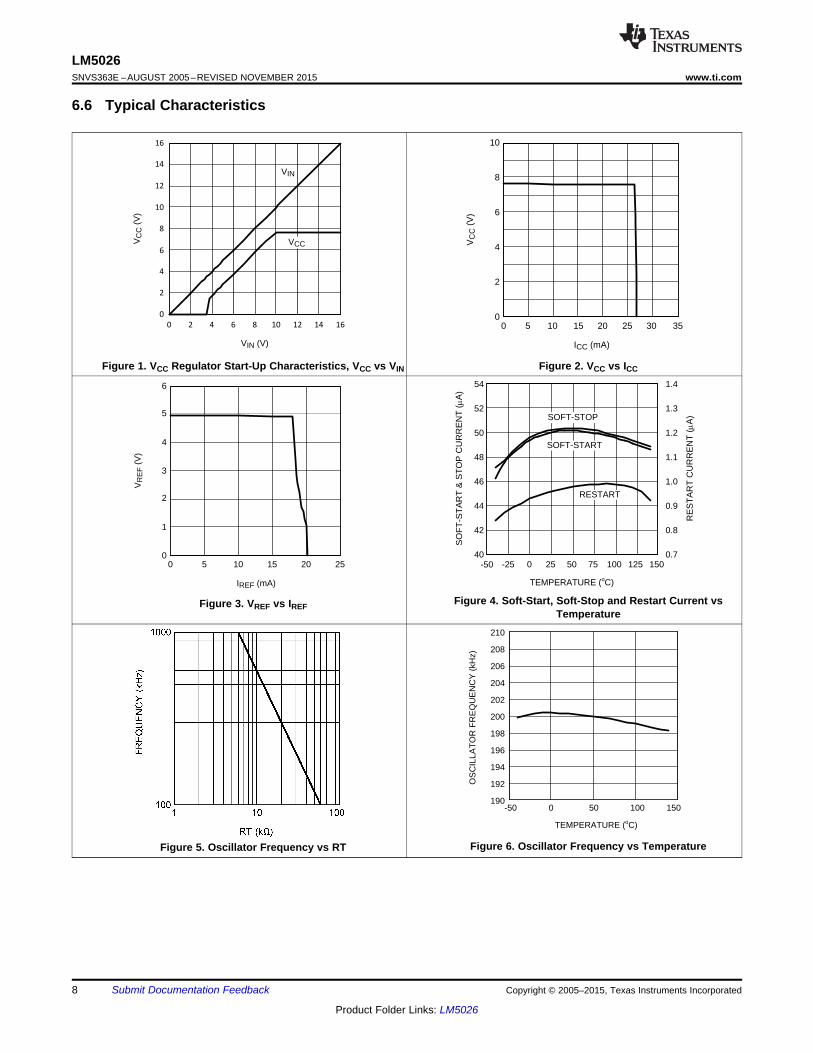
6.6 Typical Characteristics
Figure 1. VCC Regulator Start-Up Characteristics, VCC vs VIN Figure 2. VCC vs ICC
Figure 4. Soft-Start, Soft-Stop and Restart Current vsFigure 3. VREF vs IREFTemperature
Figure 6. Oscillator Frequency vs TemperatureFigure 5. Oscillator Frequency vs RT
8 Submit Documentation Feedback Copyright © 2005–2015, Texas Instruments Incorporated
Product Folder Links: LM5026

0.0 0.5 1.0 1.5 2.0 2.5 3.0 3.5 4.0 4.5 5.0
0
10
20
30
40
50
60
70
80
90
100
MA
X D
UT
Y C
YC
LE (
%)
UVLO (V)
DCL = 2.5V
0.0 0.2 0.4 0.6 0.8 1.0 1.2 1.4 1.6 1.8 2.0
0
10
20
30
40
50
60
70
80
90
100
MA
X D
UT
Y C
YC
LE (
%)
DCL (V)
UVLO = 1.26V
-50 -25 0 25 50 75 100 125 150
TEMPERATURE (oC)
80
85
90
95
100
105
110
115
120
DE
AD
TIM
E (
ns)
RSET = 30.0 k:
0 20 40 60 80 100 120
RSET (k:)
0
50
100
150
200
250
300
350
400
DE
AD
TIM
E (
ns)
RSET to REF
-50 -25 0 25 50 75 100 125 150
TEMPERATURE (oC)
80
85
90
95
100
105
110
115
120
OV
ER
LAP
TIM
E (
ns)
RSET = 34.8 k:
0 20 40 60 80 100 120
RSET (k:)
0
50
100
150
200
250
300
350
400O
VE
RLA
P T
IME
(ns
)
RSET to AGND
LM5026www.ti.com SNVS363E –AUGUST 2005–REVISED NOVEMBER 2015
Typical Characteristics (continued)
Figure 7. Overlap Time vs RSET Figure 8. Overlap Time vs Temperature
Figure 9. Deadtime vs RSET Figure 10. Deadtime vs Temperature
Figure 11. Max Duty Cycle vs UVLO Figure 12. Max Duty Cycle vs DCL
Copyright © 2005–2015, Texas Instruments Incorporated Submit Documentation Feedback 9
Product Folder Links: LM5026

-0.10 0.00 0.10 0.20 0.30 0.40 0.50
INVERTING INPUT TO PWM COMPARATOR (V)
300
400
500
600
700
800
CO
MP
CU
RR
EN
T (P
A)
125°C
85°C
25°C
-40°C
LM5026SNVS363E –AUGUST 2005–REVISED NOVEMBER 2015 www.ti.com
Typical Characteristics (continued)
Figure 13. COMP Current vs INV PWM Comparator Voltage
10 Submit Documentation Feedback Copyright © 2005–2015, Texas Instruments Incorporated
Product Folder Links: LM5026

LOGIC
VIN VCC
REF
SS
SOFT-STOP(50 PA)
RT
PGND
AGND
5VREFERENCE
OSCILLATORAND
DUTY CYCLELIMITER
DEADTIMEOR
OVERLAPCONTROL
CLK
CS
TIME
0.5V
PWM
5k
5V
1.4V
R
S Q
SS
SLOPE COMPRAMP
VCC
UVLO
7.6V BIASREGULATOR
OUT_ADRIVER
VCC
OUT_BDRIVER
COMP
RESTARTDELAY(1 PA)
SS
SYNC
UVLO
HYSTERESIS (20 PA)
1.25V
R
2R
2k
RESCURRENT LIMIT
RESTARTTIMER
&SS CONTROL
CURRENTLIMIT
45 PA
0
DCL
SHUTDOWN
0.4V/0.3V
STANDBY
1 : 1
THERMALLIMIT
CURRENTLIMITING
(10 PA)
SOFT-START(50 PA)
5V5V
5V
NOTCURRENTLIMITING(10 PA)
VCC
OUT_A + LEB
LM5026www.ti.com SNVS363E –AUGUST 2005–REVISED NOVEMBER 2015
7 Detailed Description
7.1 OverviewThe LM5026 PWM controller contains all of the features necessary to implement power converters utilizing theactive clamp reset technique with current mode control. With the active clamp reset, higher efficiencies andgreater power densities can be realized compared to conventional catch winding or RDC clamp reset techniques.The LM5026 provides two control outputs, the main power switch control (OUT_A) and the active clamp switchcontrol (OUT_B). The device can be configured to drive either a P-Channel or N-Channel clamp switch. Themain switch gate driver features a compound configuration consisting of both MOS and bipolar devices, whichprovide superior gate drive characteristics. The LM5026 can be configured to operate with bias voltages over awide input range from 8 V to 100 V. Additional features include programmable maximum duty cycle, lineundervoltage lockout, cycle-by-cycle current limit, hiccup mode fault protection with adjustable delays, PWMslope compensation, soft-start, a 1-MHz capable oscillator with synchronization input and output capability,precision reference, and thermal shutdown.
7.2 Functional Block Diagram
Copyright © 2005–2015, Texas Instruments Incorporated Submit Documentation Feedback 11
Product Folder Links: LM5026

LM5026SNVS363E –AUGUST 2005–REVISED NOVEMBER 2015 www.ti.com
7.3 Feature Description
7.3.1 High Voltage Start-Up RegulatorThe LM5026 contains an internal high voltage start-up regulator that allows the input pin (VIN) to be connecteddirectly to a nominal 48-V DC line voltage. The regulator output (VCC) is internally current limited to 20 mA.When power is applied and the UVLO pin potential is greater than 0.4 V, the regulator is enabled and sourcescurrent into an external capacitor connected to the VCC pin. The recommended capacitance range for the VCCregulator is 0.1 µF to 100 µF. The VCC regulator provides power to the internal voltage reference, PWMcontroller and gate drivers. The controller outputs are enabled when the voltage on the VCC pin reaches theregulation point of 7.6 V, the internal voltage reference (REF) reaches its regulation point of 5 V and the UVLOvoltage is greater than 1.25 V. In typical applications, an auxiliary transformer winding is connected through adiode to the VCC pin. This winding must raise the VCC voltage above 8 V to shut off the internal start-upregulator. Powering VCC from an auxiliary winding improves efficiency while reducing the controller’s powerdissipation.
The external VCC capacitor must be sized such that the current delivered from the capacitor and the VCCregulator will maintain a VCC voltage greater than 6.2 V during the initial start-up. During a fault mode when theconverter auxiliary winding is inactive, external current draw on the VCC line should be limited such that thepower dissipated in the start-up regulator does not exceed the maximum power dissipation of the IC package. Anexternal start-up or bias regulator can be used to power the LM5026 instead of the internal start-up regulator byconnecting the VCC and the VIN pins together and connecting an external bias supply to these two pins.
7.3.2 Line Undervoltage DetectorThe LM5026 contains a dual level undervoltage lockout (UVLO) circuit. When the UVLO pin voltage is below 0.4V, the controller is in a low current shutdown mode. When the UVLO pin voltage is greater than 0.4 V but lessthan 1.25 V, the controller is in standby mode. In standby mode the VCC and REF bias regulators are activewhile the controller outputs are disabled. When the VCC and REF outputs exceed the VCC and REFundervoltage thresholds and the UVLO pin voltage is greater than 1.25 V, the outputs are enabled and normaloperation begins. An external set-point voltage divider from VIN to GND can be used to set the operational rangeof the converter. The divider must be designed such that the voltage at the UVLO pin will be greater than 1.25 Vwhen VIN is in the desired operating range. UVLO hysteresis is accomplished with an internal 20-µA currentsource that is switched on or off into the impedance of the set-point divider. When the UVLO threshold isexceeded, the current source is activated to instantly raise the voltage at the UVLO pin. When the UVLO pinvoltage falls below the 1.25-V threshold, the current source is turned off causing the voltage at the UVLO pin tofall. The hysteresis of the 0.4-V shutdown comparator is fixed at 100 mV.
The UVLO pin can also be used to implement various remote enable and disable functions. Pulling the UVLO pinbelow the 0.4-V threshold totally disables the controller. Pulling the UVLO pin to a potential between 1.25 and 0.4V places the controller in standby with the VCC and REF regulators operating. Turning off a converter by forcingthe UVLO pin to the standby condition provides a controlled soft-stop. The controller outputs are not directlydisabled in standby mode, rather the soft-start capacitor is discharged with a 50-µA sink current. Discharging thesoft-start capacitor gradually reduces the PWM duty cycle to zero, providing a slow controlled discharge of thepower converter output filter. This controlled discharge can help prevent uncontrolled behavior of self-drivensynchronous rectifiers during turnoff.
7.3.3 PWM OutputsThe relative phase of the main switch gate driver OUT_A and active clamp gate driver OUT_B can be configuredfor multiple applications. For active clamp configurations utilizing a ground referenced P-Channel clamp switch,the two outputs should be in phase, with the active clamp output overlapping the main output. For active clampconfigurations utilizing a high-side N-Channel switch, the active clamp output should be out of phase with mainoutput and there should be a dead time between the two gate drive pulses. A distinguishing feature of theLM5026 is the ability to accurately configure either deadtime (both off) or overlap time (both on) of the gate driveroutputs. The overlap / deadtime magnitude is controlled by the resistor value (RSET) connected to the TIME pinof the controller. The opposite end of the resistor can be connected to either REF for deadtime control or toAGND for overlap control. The internal configuration detector senses the direction of current flow in the TIME pinresistor and configures the phase relationship of the main and active clamp outputs.
12 Submit Documentation Feedback Copyright © 2005–2015, Texas Instruments Incorporated
Product Folder Links: LM5026

PWM
VCC
OUT_A
PGND
LM5026
OUT_A
OUT_B
OUT_A
OUT_B
K1 * RSET
N-Channel Active Clamp(RSET to REF)
P-Channel Active Clamp(RSET to GND)
K2 * RSET
K1 * RSET
K2 * RSET
LM5026www.ti.com SNVS363E –AUGUST 2005–REVISED NOVEMBER 2015
Feature Description (continued)
Figure 14. PWM Output Phasing / Timing
The rising edge overlap or deadtime and the falling edge overlap or deadtime are identical and are independentof operating frequency or duty cycle. The magnitude of the overlap/deadtime can be calculated in Equation 1 andEquation 2:
Overlap Time = 2.8 × RSET + 2
where• RSET in kΩ• overlap is in ns (1)
.Deadtime = 2.9 × RSET + 14
where• RSET in kΩ• deadtime is in ns (2)
7.3.4 Gate Driver OutputsThe LM5026 provides two-gate driver outputs, the main power switch control (OUT_A) and the active clampswitch control (OUT_B). The main gate driver features a compound configuration, consisting of both MOS andbipolar devices, which provide superior gate drive characteristics. The bipolar device provides most of the drivecurrent capability and sinks a relatively constant current, which is ideal for driving large-power MOSFETs. As theswitching event nears conclusion and the bipolar device saturates, the internal MOS device provides a lowimpedance to compete the switching event.
During turnoff at the Miller plateau region, typically between 2 V to 4 V, the voltage differential between theoutput and PGND is small and the current source characteristic of the bipolar device is beneficial to reduce thetransition time. During turnon, the resistive characteristics of a purely MOS gate driver is adequate since thesupply to output voltage differential is fairly large in the Miller region.
Figure 15. Compound Gate Driver
Copyright © 2005–2015, Texas Instruments Incorporated Submit Documentation Feedback 13
Product Folder Links: LM5026

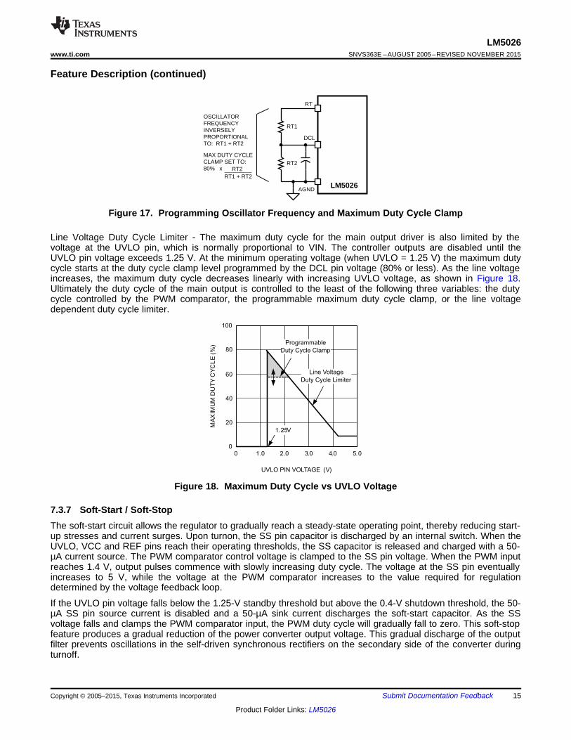
RTProgrammable Duty Cycle Clamp 80%
RT RT
2
1 2= ´
+
INVVds
D(max)
1 (max)=
-
PWMCOMPARATOR
5V
1.4VCOMP
SOFT-START
1 : 1
REF
LM431FB
Potential across Opto-coupler detector is
constant
LM5026
+
_
CURRENT SENSE RAMP
5k
2R
R
LM5026SNVS363E –AUGUST 2005–REVISED NOVEMBER 2015 www.ti.com
Feature Description (continued)7.3.5 PWM Comparator/Slope CompensationThe PWM comparator modulates the pulse width of the controller output by comparing the current sense rampsignal to the loop error signal. This comparator is optimized for speed in order to achieve minimum controllableduty cycles. The loop error signal is input into the controller in the form of a control current into the COMP pin.The COMP pin control current is internally mirrored by a matched pair of NPN transistors which sink currentthrough a 5-kΩ resistor connected to the 5-V reference. The resulting error signal passes through a 1.4-V levelshift and a gain reducing 3:1 resistor divider before being applied to the pulse width modulator.
The optocoupler detector can be connected between the REF pin and the COMP pin. Because the COMP pin iscontrolled by a current input, the potential difference across the optocoupler detector is nearly constant. Thebandwidth limiting phase delay which is normally introduced by the significant capacitance of the optocoupler isgreatly reduced. Greater system loop bandwidth can be realized, since the bandwidth-limiting pole associatedwith the optocoupler is now at a much higher frequency. The PWM comparator polarity is configured such thatwith no current into the COMP pin, the controller produces the maximum duty cycle at the main gate driveroutput.
Figure 16. Optocoupler to LM5026 COMP Interface
For duty cycles greater than 50 percent, current mode control circuits are subject to sub-harmonic oscillation. Byadding an additional fixed slope voltage ramp signal (slope compensation) to the current sense signal, thisoscillation can be avoided. The LM5026 integrates this slope compensation by summing a current rampgenerated by the oscillator with the current sense signal. The PWM comparator ramp signal is a combination ofthe current waveform at the CS pin, and an internally generated slope compensation ramp derived from theoscillator. The internal ramp has an amplitude of 0 to 45 µA which is sourced into an internal 2-kΩ resistor, plusthe external impedance at the CS pin. Additional slope compensation may be added by increasing the sourceimpedance of the current sense signal.
7.3.6 Maximum Duty Cycle ClampControlling the maximum duty cycle of an active clamp reset PWM controller is necessary to limit the voltagestress on the main and active clamp MOSFETs. The relationship between the maximum drain-source voltage ofthe MOSFETs and the maximum PWM duty cycle is provided by Equation 3:
(3)
The main output (OUT_A) duty cycle is normally controlled by the control current sourced into the COMP pinfrom the external feedback circuit. When the feedback demands maximum output from the converter, the dutycycle will be limited by one of two circuits within the LM5026: the user programmable duty cycle clamp and thevoltage-dependent duty cycle limiter, which varies inversely with the input line voltage.
Programmable Duty Cycle Clamp – The maximum allowed duty cycle can be programmed by setting a voltage atthe DCL pin to a value less than 2 V. The recommended method to set the DCL pin voltage is with a resistordivider connected from the RT pin to AGND. The voltage at the RT pin is internally regulated to 2 V, while thecurrent sourced from the RT pin sets the oscillator frequency. The maximum duty can be programmed, accordingto Equation 4:
(4)
14 Submit Documentation Feedback Copyright © 2005–2015, Texas Instruments Incorporated
Product Folder Links: LM5026
0 1.0 2.0 3.0 4.0 5.00
20
40
60
80
100
MA
XIM
UM
DU
TY
CY
CL
E(%
)
UVLO PIN VOLTAGE (V)
Programmable
Duty Cycle Clamp
Line Voltage
Duty Cycle Limiter
1.25V
RT1
RT2
DCL
RT
AGND
OSCILLATORFREQUENCYINVERSELYPROPORTIONALTO: RT1 + RT2
MAX DUTY CYCLECLAMP SET TO:80% x RT2
RT1 + RT2
LM5026
LM5026www.ti.com SNVS363E –AUGUST 2005–REVISED NOVEMBER 2015
Feature Description (continued)
Figure 17. Programming Oscillator Frequency and Maximum Duty Cycle Clamp
Line Voltage Duty Cycle Limiter - The maximum duty cycle for the main output driver is also limited by thevoltage at the UVLO pin, which is normally proportional to VIN. The controller outputs are disabled until theUVLO pin voltage exceeds 1.25 V. At the minimum operating voltage (when UVLO = 1.25 V) the maximum dutycycle starts at the duty cycle clamp level programmed by the DCL pin voltage (80% or less). As the line voltageincreases, the maximum duty cycle decreases linearly with increasing UVLO voltage, as shown in Figure 18.Ultimately the duty cycle of the main output is controlled to the least of the following three variables: the dutycycle controlled by the PWM comparator, the programmable maximum duty cycle clamp, or the line voltagedependent duty cycle limiter.
Figure 18. Maximum Duty Cycle vs UVLO Voltage
7.3.7 Soft-Start / Soft-StopThe soft-start circuit allows the regulator to gradually reach a steady-state operating point, thereby reducing start-up stresses and current surges. Upon turnon, the SS pin capacitor is discharged by an internal switch. When theUVLO, VCC and REF pins reach their operating thresholds, the SS capacitor is released and charged with a 50-µA current source. The PWM comparator control voltage is clamped to the SS pin voltage. When the PWM inputreaches 1.4 V, output pulses commence with slowly increasing duty cycle. The voltage at the SS pin eventuallyincreases to 5 V, while the voltage at the PWM comparator increases to the value required for regulationdetermined by the voltage feedback loop.
If the UVLO pin voltage falls below the 1.25-V standby threshold but above the 0.4-V shutdown threshold, the 50-µA SS pin source current is disabled and a 50-µA sink current discharges the soft-start capacitor. As the SSvoltage falls and clamps the PWM comparator input, the PWM duty cycle will gradually fall to zero. This soft-stopfeature produces a gradual reduction of the power converter output voltage. This gradual discharge of the outputfilter prevents oscillations in the self-driven synchronous rectifiers on the secondary side of the converter duringturnoff.
Copyright © 2005–2015, Texas Instruments Incorporated Submit Documentation Feedback 15
Product Folder Links: LM5026

LM5026SNVS363E –AUGUST 2005–REVISED NOVEMBER 2015 www.ti.com
Feature Description (continued)7.3.8 Current Sense and Current LimitThe CS input provides a control ramp for the pulse width modulator and current limit detection for overloadprotection. If the sensed voltage at the CS comparator exceeds 0.5 V, the present cycle is terminated (cycle-by-cycle current limit mode).
A small RC filter, located near the controller, is recommended for the CS input pin. An internal FET connected tothe CS input discharges the current sense filter capacitor at the conclusion of every cycle to improve dynamicperformance. This same FET remains on for an additional 100 nS at the start of each main switch cycle toattenuate the leading edge spike in the current sense signal.
The CS comparator is very fast and may respond to short duration noise pulses. Layout considerations arecritical for the current sense filter and sense resistor. The capacitor associated with the CS filter must be placedvery close to the device and connected directly to the pins of the LM5026 (CS and AGND pins). If a currentsense transformer is used, both leads of the transformer secondary should be routed to the filter network, whichshould be located close to the IC. If a sense resistor located in the source of the main switch MOSFET is usedfor current sensing, a low inductance type of resistor is required. When designing with a current sense resistor,all of the noise-sensitive, low-power ground connections should be connected together near the AGND pin and asingle connection should be made to the power ground (sense resistor ground point).
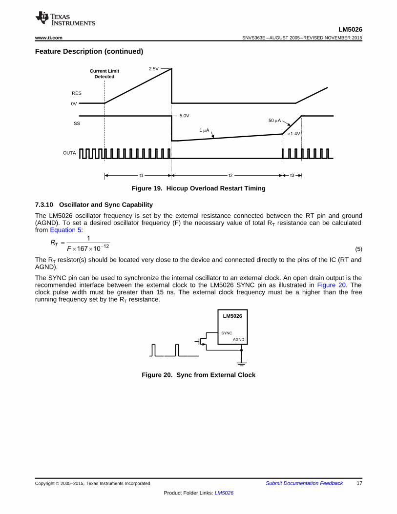
7.3.9 Overload Protection TimerThe LM5026 provides a current limit restart timer to disable the outputs and force a delayed restart (hiccupmode) if a current limit condition is repeatedly sensed. The number of cycle-by-cycle current limit events requiredto trigger the restart is programmable by means of an external capacitor at the RES pin. During each PWM cyclethe LM5026 either sources or sinks current from the RES pin capacitor. If no current limit is detected during acycle, a 10-µA discharge current sink is enabled to hold the RES pin at ground. If a current limit is detected, the10-µA sink current is disabled and a 10-µA current source causes the voltage at RES pin to gradually increase.In the event of an extended overload condition, the LM5026 protects the converter with cycle-by-cycle currentlimiting while the voltage at RES pin increases. If the RES voltage reaches the 2.5-V threshold, the followingrestart sequence occurs (see Figure 19):• The RES capacitor and SS capacitors are fully discharged.• The soft-start current source is reduced from 50 µA to 1 µA• The SS capacitor voltage slowly increases. When the SS voltage reaches 1.4 V, the PWM comparator will
produce the first output pulse. After the first pulse occurs, the SS source current reverts to the normal 50 µAlevel. The SS voltage increases at its normal rate gradually increasing the duty cycle of the output drivers
• If the overload condition persists after restart, cycle-by-cycle current limiting will cause the voltage on the REScapacitor to increase again, repeating the hiccup mode sequence.
• If the overload condition no longer exists after restart, the RES pin will be held at ground by the 10-µA currentsink and normal operation resumes.
The overload timer function is very versatile and can be configured for the following modes of protection:1. Cycle-by-cycle only: The hiccup mode can be completely disabled by connecting the RES pin to AGND. In
this configuration, the cycle-by-cycle protection will limit the output current indefinitely and no hiccupsequences will occur.
2. Hiccup only: The timer can be configured for immediate activation of a hiccup sequence upon detection ofan overload by leaving the RES pin open circuit.
3. Delayed Hiccup: The most common configuration as previously described, is a programmed interval ofcycle-by-cycle limiting before initiating a hiccup mode restart. The advantage of this configuration is short-term overload conditions will not cause a hiccup mode restart, however during extended overload conditionsthe average dissipation of the power converter will be very low.
4. Externally Controlled Hiccup: The RES pin can also be used as an input. By externally driving the pin to alevel greater than the 2.5-V hiccup threshold, the controller will be forced into the delayed restart sequence.If the RES pin is used as an input, the driving source should be current limited to less than 5 mA. Forexample, the external trigger for a delayed restart sequence could come an overtemperature protectioncircuit.
16 Submit Documentation Feedback Copyright © 2005–2015, Texas Instruments Incorporated
Product Folder Links: LM5026
SYNC
AGND
LM5026
TR
F12
1
167 10-
=
´ ´
RES
SS
OUTA
0V
2.5V
#1.4V
5.0V
t1 t2 t3
Current LimitDetected
50 PA
1 PA
LM5026www.ti.com SNVS363E –AUGUST 2005–REVISED NOVEMBER 2015
Feature Description (continued)
Figure 19. Hiccup Overload Restart Timing
7.3.10 Oscillator and Sync CapabilityThe LM5026 oscillator frequency is set by the external resistance connected between the RT pin and ground(AGND). To set a desired oscillator frequency (F) the necessary value of total RT resistance can be calculatedfrom Equation 5:
(5)
The RT resistor(s) should be located very close to the device and connected directly to the pins of the IC (RT andAGND).
The SYNC pin can be used to synchronize the internal oscillator to an external clock. An open drain output is therecommended interface between the external clock to the LM5026 SYNC pin as illustrated in Figure 20. Theclock pulse width must be greater than 15 ns. The external clock frequency must be a higher than the freerunning frequency set by the RT resistance.
Figure 20. Sync from External Clock
Copyright © 2005–2015, Texas Instruments Incorporated Submit Documentation Feedback 17
Product Folder Links: LM5026

SYNC
200P
S
R
Q
Q
DEADTIMEONE-SHOT
I = f (RT)2V
CLK
SYNC
LM5026
SYNC
LM5026
UP TO 5 TOTALDEVICES
LM5026SNVS363E –AUGUST 2005–REVISED NOVEMBER 2015 www.ti.com
Feature Description (continued)
Figure 21. Sync from Multiple Devices
Multiple LM5026 devices can be synchronized together simply by connecting the devices SYNC pins together asshown in Figure 21. Take care to ensure the ground potential differences between devices are minimized. In thisconfiguration all of the devices will be synchronized to the highest frequency device. The internal block diagramof the oscillator and synchronization circuit is shown in Figure 22. The SYNC I/O pin is a CMOS buffer withpullup current limited to 200 µA. If an external device forces the SYNC pin low before the internal oscillator rampcompletes its charging cycle, the ramp will be reset and another cycle begins. If the SYNC pins of multipleLM5026 devices are connected together, the first SYNC pin that pulls low will reset the oscillator RAMP of allother devices. All controllers will operate in phase when synchronized using the SYNC I/O feature. Up to fiveLM5026 devices can be synchronized using this technique.
Figure 22. Oscillator Sync I/O Block Diagram
7.3.11 Thermal ProtectionInternal Thermal Shutdown circuitry is provided to protect the integrated circuit in the event the maximum junctiontemperature is exceeded. When activated, typically at 165°C, the controller is forced into a low power standbystate with the output drivers and the bias regulator disabled. The device will restart after the thermal hysteresis(typically 25°C). During thermal shutdown, the soft-start capacitor is fully discharged and the controller follows anormal start-up sequence after the junction temperature falls to the operating level.
18 Submit Documentation Feedback Copyright © 2005–2015, Texas Instruments Incorporated
Product Folder Links: LM5026
UVLO
Soft Start
Thermal Shut Down
Hiccup
Normal Operation
LM5026www.ti.com SNVS363E –AUGUST 2005–REVISED NOVEMBER 2015
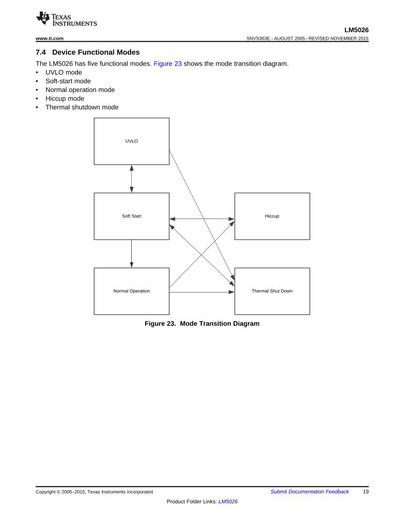
7.4 Device Functional ModesThe LM5026 has five functional modes. Figure 23 shows the mode transition diagram.• UVLO mode• Soft-start mode• Normal operation mode• Hiccup mode• Thermal shutdown mode
Figure 23. Mode Transition Diagram
Copyright © 2005–2015, Texas Instruments Incorporated Submit Documentation Feedback 19
Product Folder Links: LM5026

VPWR
VIN VCC8V - 15V (from
aux winding)C1
LM5026
9V 0.1
0.1 PF
50
LM5026
VIN
VPWR
LM5026SNVS363E –AUGUST 2005–REVISED NOVEMBER 2015 www.ti.com
8 Application and Implementation
NOTEInformation in the following applications sections is not part of the TI componentspecification, and TI does not warrant its accuracy or completeness. TI’s customers areresponsible for determining suitability of components for their purposes. Customers shouldvalidate and test their design implementation to confirm system functionality.
8.1 Application Information
8.1.1 Line Input (VIN)The LM5026 contains an internal high voltage start-up regulator that allows the input pin (VIN) to be connecteddirectly to a nominal 48-V line voltage. The voltage applied to the VIN pin can vary in the range of 13 to 100 Vwith transient capability to 105 V. When power is applied and the UVLO pin potential is greater than 0.4 V, theVCC regulator is enabled and sources current into an external capacitor connected to the VCC pin. When thevoltage on the VCC pin reaches the regulation point of 7.7 V, the internal voltage reference (REF) is enabled.The reference regulation set-point is 5 V. The controller outputs are enabled when the UVLO pin potential isgreater than 1.25 V. In typical applications, an auxiliary transformer winding is connected through a diode to theVCC pin. This winding must raise the VCC voltage above 8 V to shut off the internal start-up regulator. TIrecommends a filtering circuit shown in Figure 24 be used to suppress transients, which may occur at the inputsupply, in particular when VIN is operated close to the maximum operating rating.
Figure 24. Input Transient Protection
8.1.2 For Application > 100 VFor applications where the system input voltage exceed 100 V or IC power dissipation is a concern, the LM5026can be powered from an external start-up regulator as shown in Figure 25. In this configuration, the VIN and theVCC pins should be connected together, which allows the LM5026 to be operated below 13 V. The voltage at theVCC pin must be greater than 8 V yet not exceed 15 V. An auxiliary winding can be used to reduce thedissipation in the external regulator once the power converter is active.
Figure 25. Start-Up Regulator for VPWR >100 V
20 Submit Documentation Feedback Copyright © 2005–2015, Texas Instruments Incorporated
Product Folder Links: LM5026

UVLO
LM5026
VPWR
1.25V
20 PA
Enable
R1
R2
0.4VStandby
OFF
STANDBY
UVLO
LM5026
VPWR
1.25V
20 PA
Enable Output Drivers
R1
R2
0.4V
Enable VCC & VREF
Regulators
PWR
1.25 R1R2
V 1.25
´
=
-
HYSVR1
20 A=
m
LM5026www.ti.com SNVS363E –AUGUST 2005–REVISED NOVEMBER 2015
Application Information (continued)8.1.3 Undervoltage Lockout (UVLO)When the UVLO pin voltage is below 0.4 V, the controller is in a low current shutdown mode. When the UVLOpin voltage is greater than 0.4 V but less than 1.25 V, the controller is in standby mode. When the UVLO pinvoltage is greater than 1.25 V, the controller is fully enabled. Typically, two external resistors program theminimum operational voltage for the power converter as shown in Figure 26. When UVLO pin voltage is abovethe 1.25-V threshold, an internal 20-μA current source is enabled to raise the voltage at the UVLO pin, thusproviding threshold hysteresis. Resistance values for R1 and R2 can be determined from Equation 6 andEquation 7:
where• VHYS is the desired UVLO hysteresis at VPWR (6)
.
where• VPWR is the desired turnon voltage (7)
For example, if the LM5026 is to be enabled when VPWR reaches 33 V, and disabled when VPWR is decreased to30 V, R1 calculates to 150 kΩ, and R2 calculates to 5.9 kΩ. The voltage at the UVLO pin should not exceed 6 Vat any time. Be sure to check both the power and voltage rating for the selected R1 resistor.
Remote configuration of the controller’s operational modes can be accomplished with open drain device(s)connected to the UVLO pin as shown in Figure 27.
Figure 26. Basic UVLO Configuration
Figure 27. Remote Standby and Disable Control
Copyright © 2005–2015, Texas Instruments Incorporated Submit Documentation Feedback 21
Product Folder Links: LM5026

VPWR
LM5026CS
OUTA
AGND
VIN
OUTB
R1
RF
CF
PowerTransformer
CurrentSense
Q1 Q2
LM5026SNVS363E –AUGUST 2005–REVISED NOVEMBER 2015 www.ti.com
Application Information (continued)8.1.4 Oscillator (RT, SYNC)Oscillator (RT, SYNC) The oscillator frequency is generally selected in conjunction with the design of the systemmagnetic components along with the volume and efficiency goals for a given power converter design. The totalRT resistance at the RT pin sets the oscillator frequency. The RT resistors should be one of the first componentsplaced and connected when designing the PCB. Direct, short connections to each side of the RT resistors (RT,DCL and AGND pins) are recommended .
The SYNC pin can be used to synchronize the internal oscillator to an external clock. An open-drain output is therecommended interface from the external clock to the SYNC pin. The clock pulse width should be greater than15 ns. The external clock must be a higher frequency than the free-running frequency set by the RT resistor.Multiple LM5026 devices can be synchronized together simply by connecting the devices SYNC pins together.Take care to ensure the ground potential differences between devices are minimized. In this configuration all ofthe devices will be synchronized to the highest frequency device.
8.1.5 Voltage Feedback (COMP)The COMP pin is designed to accept the voltage loop feedback error signal from the regulated output through anerror amplifier and (typically) an optocoupler. In a typical configuration, VOUT is compared to a precisionreference voltage by the error amplifier. The output of the amplifier drives the optocoupler, which in turn drivesthe COMP pin. The parasitic capacitance of the optocoupler often limits the achievable loop bandwidth for agiven power converter. The optocoupler LED and detector junction capacitance produce a low-frequency pole inthe voltage regulation loop. The LM5026 current controlled optocoupler interface (COMP) previously described,greatly increases the pole frequency associated with the optocoupler.
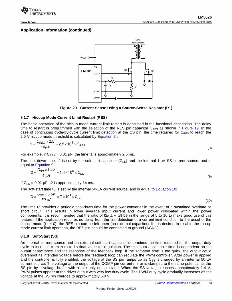
8.1.6 Current Sense (CS)The CS pin receives an input signal representative of the transformer primary current, either from a current sensetransformer (Figure 28) or from a resistor in series with the source of the primary switch (Figure 29). In bothcases the sensed current creates a ramping voltage across R1, while the RF/CF filter suppresses noise andtransients. R1, RF and CF should be as physically close to the LM5026 as possible, and the ground connectionfrom the current sense transformer, or R1, should be a dedicated track to the AGND pin. The current-sensecomponents must provide > 0.5 V at the CS pin when an overcurrent condition exists.
Figure 28. Current Sense Using a Current-Sense Transformer
22 Submit Documentation Feedback Copyright © 2005–2015, Texas Instruments Incorporated
Product Folder Links: LM5026
SSSS
C Vt C
50 A
43.53 7 10
´= = ´ ´
m
SSSS
C Vt C
A
61.42 1.4 10
1
´= = ´ ´
m
RESRES
Ct C
A
52.51 2.5 10
10
´= = ´ ´
m
VPWR
LM5026
CS
OUTA
AGND
VIN
OUTB
RF
CF
Q1 Q2
R1
PowerTransformer
LM5026www.ti.com SNVS363E –AUGUST 2005–REVISED NOVEMBER 2015
Application Information (continued)
Figure 29. Current Sense Using a Source-Sense Resistor (R1)
8.1.7 Hiccup Mode Current Limit Restart (RES)The basic operation of the hiccup mode current limit restart is described in the functional description. The delaytime to restart is programmed with the selection of the RES pin capacitor CRES as shown in Figure 19. In thecase of continuous cycle-by-cycle current limit detection at the CS pin, the time required for CRES to reach the2.5-V hiccup mode threshold is calculated by Equation 8 :
(8)
For example, if CRES = 0.01 µF, the time t1 is approximately 2.5 ms.
The cool down time, t2 is set by the soft-start capacitor (CSS) and the internal 1-µA SS current source, and isequal to Equation 9:
(9)
If CSS = 0.01 µF, t2 is approximately 14 ms.
The soft-start time t3 is set by the internal 50-µA current source, and is equal to Equation 10:
(10)
The time t2 provides a periodic cool-down time for the power converter in the event of a sustained overload orshort circuit. This results in lower average input current and lower power dissipated within the powercomponents. It is recommended that the ratio of t2/(t1 + t3) be in the range of 5 to 10 to make good use of thisfeature. If the application requires no delay from the first detection of a current limit condition to the onset of thehiccup mode (t1 = 0), the RES pin can be left open (no external capacitor). If it is desired to disable the hiccupmode current limit operation, the RES pin should be connected to ground (AGND).
8.1.8 Soft-Start (SS)An internal current source and an external soft-start capacitor determines the time required for the output dutycycle to increase from zero to its final value for regulation. The minimum acceptable time is dependent on theoutput capacitance and the response of the feedback loop. If the soft-start time is too quick, the output couldovershoot its intended voltage before the feedback loop can regulate the PWM controller. After power is appliedand the controller is fully enabled, the voltage at the SS pin ramps up as CSS is charged by an internal 50-µAcurrent source. The voltage at the output of the COMP pin current mirror is clamped to the same potential as theSS pin by a voltage buffer with a sink-only output stage. When the SS voltage reaches approximately 1.4 V,PWM pulses appear at the driver output with very low duty cycle. The PWM duty cycle gradually increases as thevoltage at the SS pin charges to approximately 5.0 V.
Copyright © 2005–2015, Texas Instruments Incorporated Submit Documentation Feedback 23
Product Folder Links: LM5026

UVLO
LM5026
VPWR
1.25V
Max. DutyCycle Limiter
R1A
R1B
R2
Z1
UVLO
LM5026
1.25V
20 PA
Max. DutyCycle Limiter
R1
R2
Z1
20 PA
VPWR
LM5026SNVS363E –AUGUST 2005–REVISED NOVEMBER 2015 www.ti.com
Application Information (continued)8.1.9 Voltage-Dependent Maximum Duty CycleAs the input source VPWR increases the voltage at the UVLO pin increases proportionately. To limit the Volt ×Seconds applied to the transformer, the maximum allowed PWM duty cycle decreases as the UVLO voltageincreases. If it is desired to increase the slope of the voltage limited duty cycle characteristic, two possibleconfigurations are shown in Figure 30. After the LM5026 is enabled, the zener diode causes the UVLO pinvoltage to increase more rapidly with increasing input voltage (VPWR). The voltage dependent maximum dutycycle clamp varies with the UVLO pin voltage according to Equation 11:
Voltage-Dependent Duty Cycle (%) = 107 - 21.8 X UVLO (11)
Figure 30. Altering the Slope of Duty Cycle vs VPWR
8.1.9.1 Programmable Maximum Duty Cycle Clamp (DCL)When the UVLO pin is biased at 1.25 V (minimum operating level), the maximum duty cycle of OUT_A is limitedby the duty cycle of the internal clock signal. The duty cycle of the internal clock can be adjusted byprogramming a voltage set at the DCL pin. The default maximum duty cycle (80%) can be selected byconnecting the DCL pin to the RT pin. The DCL pin should not be left open. A small decoupling capacitor locatedclose to the DCL pin is recommended.
The oscillator frequency set resistance (RT) must be determined first before programming the maximum dutycycle. Following the selection of the total RT resistance, the ratio of the RT resistors can be designed to set thedesired maximum duty cycle. As the UVLO pin voltage increases from 1.25 V, the maximum duty cycle isreduced by the voltage dependent duty cycle limiter previously as described and shown in Figure 18.
24 Submit Documentation Feedback Copyright © 2005–2015, Texas Instruments Incorporated
Product Folder Links: LM5026
LM5026www.ti.com SNVS363E –AUGUST 2005–REVISED NOVEMBER 2015
8.2 Typical ApplicationThe following schematic shows an example of an LM5026 controlled 100-W active clamp forward powerconverter. The input voltage range (VPWR) is 36 V to 78 V, and the output voltage is 3.3 V. The output currentcapability is 30 Amps. Current sense transformer T2 provides information to the CS pin for current mode controland current limit protection. The error amplifiers and reference U3 and U4 provide voltage feedback throughoptocoupler U2. Synchronous rectifiers Q3-Q6 minimize rectification losses in the secondary. An auxiliarywinding on inductor L2 provides power to the LM5026 VCC pin when the output is in regulation. The inputvoltage UVLO levels are approximately 34 V for increasing VPWR, and ≈32 V for decreasing VPWR. The circuit canbe shut down by forcing the ON/OFF input (J2) below 1.25 V. An external synchronizing frequency can beapplied to the SYNC input (J11) or like converters can be self-synchronized by connections of (J3). The regulatoroutput is current limited at approximately 32 A.
Copyright © 2005–2015, Texas Instruments Incorporated Submit Documentation Feedback 25
Product Folder Links: LM5026

LM5026SNVS363E –AUGUST 2005–REVISED NOVEMBER 2015 www.ti.com
Figure 31. Application Circuit: Input 36 V to 78 V, Output 3.3 V, 30 A
26 Submit Documentation Feedback Copyright © 2005–2015, Texas Instruments Incorporated
Product Folder Links: LM5026

LM5026www.ti.com SNVS363E –AUGUST 2005–REVISED NOVEMBER 2015
8.2.1 Design RequirementsThe design requirements of this application are as follows:• Input range: 36 V to 78 V• Output voltage: 3.3 V• Output current: 0 to 30 A• Measured efficiency: 90% at 30 A, 92.5% at 15 A• Frequency of operation: 230 kHz• Board size: 2.3 × 2.4 × 0.5 inches• Load Regulation: 1%• Line Regulation: 0.1%• Line UVLO, Hiccup Current Limit
8.2.2 Detailed Design Procedure
8.2.2.1 Determine VIN ConfigurationFirst, determine the input voltage range of the application. If the maximum input voltage is less than 100 V, useVIN pin connection in Figure 24. If the maximum input voltage exceeds 100 V, use the configuration shown inFigure 25.
8.2.2.2 Determine UVLO ConfigurationAs described in Undervoltage Lockout (UVLO), two external resistors program the minimum operational voltagefor the power converter. Use Equation 6 and Equation 7 to calculate the resistor values. If remote standby anddisable control is needed, use the configuration in Figure 27.
8.2.2.3 Configure Operating FrequencyIf internal oscillator is used, use Equation 5 to determine the RT resistor value. If external clock is used, use theconfiguration in Figure 20.
8.2.2.4 Configure Hiccup Mode and Soft StartThe delay time to restart is programmed with the selection of the RES pin capacitor. Soft-start time isprogrammed by the capacitor on SS pin. Refer to Hiccup Mode Current Limit Restart (RES) and Equation 8,Equation 9, and Equation 10 to determine the capacitor values.
8.2.2.5 Determine Deadtime and Maximum Duty CycleThe PWM output phasing the timing is shown in Figure 14. Use Equation 1 and Equation 2 to determine thedeadtime programming resistor value. Maximum duty cycle clamp is determined by DCL pin voltage. UseEquation 4 and Figure 17 to determine RT1 and RT2 values.
Copyright © 2005–2015, Texas Instruments Incorporated Submit Documentation Feedback 27
Product Folder Links: LM5026

1
1
2
1
1
1
LM5026SNVS363E –AUGUST 2005–REVISED NOVEMBER 2015 www.ti.com
8.2.3 Application Curves
Input Voltage = 48VDCInput Voltage = 48VDC Output Current = 5 A to 25 AOutput Current = 5 A Trace 1: Output Voltage V/div = 0.5 VTrace 1: Output Voltage V/div = 1 V Trace 2: Output Current, A/div = 5 VHorizontal Resolution = 1 ms/div Horizontal Resolution = 1 ms/div
Figure 32. Output Voltage Figure 33. Transient Response
Input Voltage = 48VDCOutput Current = 30 A Input Voltage = 38VDCBandwidth Limit = 25 MHz Output Current = 25 ATrace 1: Output Voltage V/div = 50 mV Trace 1: Q1 Drain Voltage V/div = 20 VHorizontal Resolution = 2 µs/div Horizontal Resolution = 1 µs/div
Figure 34. Typical Output Ripple Figure 35. Drain Voltage of Q1
Input Voltage = 48VDCOutput Current = 5 ASynchronous Rectifier, Q3 Gate V/div = 5 V Trance 1Input Voltage = 78VDCSynchronous Rectifier, Q3 Gate V/div = 5 V Trance 2Output Current = 25 ASynchronous Rectifier, Q5 Gate V/div = 5 VTrace 1: Q1 Drain Voltage V/div = 20 VHorizontal Resolution = 1 µs/divHorizontal Resolution = 1 µs/div
Figure 37. Gate VoltagesFigure 36. Drain Voltage of Q1
28 Submit Documentation Feedback Copyright © 2005–2015, Texas Instruments Incorporated
Product Folder Links: LM5026

LM5026www.ti.com SNVS363E –AUGUST 2005–REVISED NOVEMBER 2015
9 Power Supply RecommendationsVCC pin is the power supply for the device. There should be a 0.1-µF to 100-μF capacitor directly from VCC toground. REF pin should be bypassed to ground as close as possible to the device using a 0.1-μF capacitor.
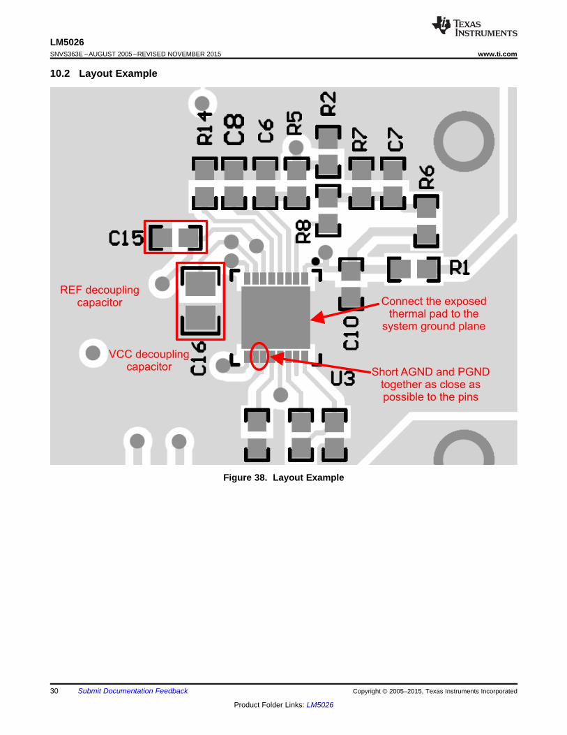
10 Layout
10.1 Layout GuidelinesThe LM5026 current-sense and PWM comparators are very fast, and respond to short duration noise pulses. Thecomponents at the CS, COMP, SS, DCL, UVLO, TIME, SYNC and the RT pins should be as physically close aspossible to the IC, thereby minimizing noise pick-up on the PCB tracks.
Layout considerations are critical for the current-sense filter. If a current-sense transformer is used, both leads ofthe transformer secondary should be routed to the sense filter components and to the IC pins. The ground sideof each transformer should be connected through a dedicated PCB track to the AGND pin, rather than throughthe ground plane.
If the current-sense circuit employs a sense resistor in the drive transistor source, low inductance resistor shouldbe used. In this case, all the noise-sensitive, low-current ground tracks should be connected in common near theIC, and then a single connection made to the power ground (sense resistor ground point). The gate drive outputsof the LM5026 should have short direct paths to the power MOSFETs in order to minimize inductance in the PCBtraces.
The two ground pins (AGND, PGND) must be connected together with a short direct connection to avoid jitterdue to relative ground bounce.
If the internal dissipation of the LM5026 produces high junction temperatures during normal operation, the use ofmultiple vias under the IC to a ground place can help conduct heat away from the IC. Judicious positioning of thePCB within the end product, along with use of any available air flow (forced or natural convection) can helpreduce the junction temperatures.
Copyright © 2005–2015, Texas Instruments Incorporated Submit Documentation Feedback 29
Product Folder Links: LM5026
REF decouplingcapacitor
VCC decouplingcapacitor
Short AGND and PGNDtogether as close aspossible to the pins
Connect the exposedthermal pad to the
system ground plane
LM5026SNVS363E –AUGUST 2005–REVISED NOVEMBER 2015 www.ti.com
10.2 Layout Example
Figure 38. Layout Example
30 Submit Documentation Feedback Copyright © 2005–2015, Texas Instruments Incorporated
Product Folder Links: LM5026
LM5026www.ti.com SNVS363E –AUGUST 2005–REVISED NOVEMBER 2015
11 Device and Documentation Support
11.1 Community ResourcesThe following links connect to TI community resources. Linked contents are provided "AS IS" by the respectivecontributors. They do not constitute TI specifications and do not necessarily reflect TI's views; see TI's Terms ofUse.
TI E2E™ Online Community TI's Engineer-to-Engineer (E2E) Community. Created to foster collaborationamong engineers. At e2e.ti.com, you can ask questions, share knowledge, explore ideas and helpsolve problems with fellow engineers.
Design Support TI's Design Support Quickly find helpful E2E forums along with design support tools andcontact information for technical support.
11.2 TrademarksE2E is a trademark of Texas Instruments.All other trademarks are the property of their respective owners.
11.3 Electrostatic Discharge CautionThese devices have limited built-in ESD protection. The leads should be shorted together or the device placed in conductive foamduring storage or handling to prevent electrostatic damage to the MOS gates.
11.4 GlossarySLYZ022 — TI Glossary.
This glossary lists and explains terms, acronyms, and definitions.
12 Mechanical, Packaging, and Orderable InformationThe following pages include mechanical, packaging, and orderable information. This information is the mostcurrent data available for the designated devices. This data is subject to change without notice and revision ofthis document. For browser-based versions of this data sheet, refer to the left-hand navigation.
Copyright © 2005–2015, Texas Instruments Incorporated Submit Documentation Feedback 31
Product Folder Links: LM5026

PACKAGE OPTION ADDENDUM
www.ti.com 14-Aug-2015
Addendum-Page 1
PACKAGING INFORMATION
Orderable Device Status(1)
Package Type PackageDrawing
Pins PackageQty
Eco Plan(2)
Lead/Ball Finish(6)
MSL Peak Temp(3)
Op Temp (°C) Device Marking(4/5)
Samples
LM5026MT NRND TSSOP PW 16 92 TBD Call TI Call TI -40 to 125 LM5026MT
LM5026MT/NOPB ACTIVE TSSOP PW 16 92 Green (RoHS& no Sb/Br)
CU NIPDAU | CU SN Level-1-260C-UNLIM -40 to 125 LM5026MT
LM5026MTX/NOPB ACTIVE TSSOP PW 16 2500 Green (RoHS& no Sb/Br)
CU NIPDAU | CU SN Level-1-260C-UNLIM -40 to 125 LM5026MT
LM5026SD/NOPB ACTIVE WSON NHQ 16 1000 Green (RoHS& no Sb/Br)
CU SN Level-1-260C-UNLIM 5026SD
LM5026SDX/NOPB ACTIVE WSON NHQ 16 4500 Green (RoHS& no Sb/Br)
CU SN Level-1-260C-UNLIM 5026SD
(1) The marketing status values are defined as follows:ACTIVE: Product device recommended for new designs.LIFEBUY: TI has announced that the device will be discontinued, and a lifetime-buy period is in effect.NRND: Not recommended for new designs. Device is in production to support existing customers, but TI does not recommend using this part in a new design.PREVIEW: Device has been announced but is not in production. Samples may or may not be available.OBSOLETE: TI has discontinued the production of the device.
(2) Eco Plan - The planned eco-friendly classification: Pb-Free (RoHS), Pb-Free (RoHS Exempt), or Green (RoHS & no Sb/Br) - please check http://www.ti.com/productcontent for the latest availabilityinformation and additional product content details.TBD: The Pb-Free/Green conversion plan has not been defined.Pb-Free (RoHS): TI's terms "Lead-Free" or "Pb-Free" mean semiconductor products that are compatible with the current RoHS requirements for all 6 substances, including the requirement thatlead not exceed 0.1% by weight in homogeneous materials. Where designed to be soldered at high temperatures, TI Pb-Free products are suitable for use in specified lead-free processes.Pb-Free (RoHS Exempt): This component has a RoHS exemption for either 1) lead-based flip-chip solder bumps used between the die and package, or 2) lead-based die adhesive used betweenthe die and leadframe. The component is otherwise considered Pb-Free (RoHS compatible) as defined above.Green (RoHS & no Sb/Br): TI defines "Green" to mean Pb-Free (RoHS compatible), and free of Bromine (Br) and Antimony (Sb) based flame retardants (Br or Sb do not exceed 0.1% by weightin homogeneous material)
(3) MSL, Peak Temp. - The Moisture Sensitivity Level rating according to the JEDEC industry standard classifications, and peak solder temperature.
(4) There may be additional marking, which relates to the logo, the lot trace code information, or the environmental category on the device.
(5) Multiple Device Markings will be inside parentheses. Only one Device Marking contained in parentheses and separated by a "~" will appear on a device. If a line is indented then it is a continuationof the previous line and the two combined represent the entire Device Marking for that device.

PACKAGE OPTION ADDENDUM
www.ti.com 14-Aug-2015
Addendum-Page 2
(6) Lead/Ball Finish - Orderable Devices may have multiple material finish options. Finish options are separated by a vertical ruled line. Lead/Ball Finish values may wrap to two lines if the finishvalue exceeds the maximum column width.
Important Information and Disclaimer:The information provided on this page represents TI's knowledge and belief as of the date that it is provided. TI bases its knowledge and belief on informationprovided by third parties, and makes no representation or warranty as to the accuracy of such information. Efforts are underway to better integrate information from third parties. TI has taken andcontinues to take reasonable steps to provide representative and accurate information but may not have conducted destructive testing or chemical analysis on incoming materials and chemicals.TI and TI suppliers consider certain information to be proprietary, and thus CAS numbers and other limited information may not be available for release.
In no event shall TI's liability arising out of such information exceed the total purchase price of the TI part(s) at issue in this document sold by TI to Customer on an annual basis.

TAPE AND REEL INFORMATION
*All dimensions are nominal
Device PackageType
PackageDrawing
Pins SPQ ReelDiameter
(mm)
ReelWidth
W1 (mm)
A0(mm)
B0(mm)
K0(mm)
P1(mm)
W(mm)
Pin1Quadrant
LM5026MTX/NOPB TSSOP PW 16 2500 330.0 12.4 6.95 5.6 1.6 8.0 12.0 Q1
LM5026SD/NOPB WSON NHQ 16 1000 178.0 12.4 5.3 5.3 1.3 8.0 12.0 Q1
LM5026SDX/NOPB WSON NHQ 16 4500 330.0 12.4 5.3 5.3 1.3 8.0 12.0 Q1
PACKAGE MATERIALS INFORMATION
www.ti.com 6-Nov-2015
Pack Materials-Page 1

*All dimensions are nominal
Device Package Type Package Drawing Pins SPQ Length (mm) Width (mm) Height (mm)
LM5026MTX/NOPB TSSOP PW 16 2500 367.0 367.0 35.0
LM5026SD/NOPB WSON NHQ 16 1000 210.0 185.0 35.0
LM5026SDX/NOPB WSON NHQ 16 4500 367.0 367.0 35.0
PACKAGE MATERIALS INFORMATION
www.ti.com 6-Nov-2015
Pack Materials-Page 2


MECHANICAL DATA
NHQ0016A
www.ti.com
SDA16A (Rev A)

IMPORTANT NOTICE
Texas Instruments Incorporated and its subsidiaries (TI) reserve the right to make corrections, enhancements, improvements and otherchanges to its semiconductor products and services per JESD46, latest issue, and to discontinue any product or service per JESD48, latestissue. Buyers should obtain the latest relevant information before placing orders and should verify that such information is current andcomplete. All semiconductor products (also referred to herein as “components”) are sold subject to TI’s terms and conditions of salesupplied at the time of order acknowledgment.TI warrants performance of its components to the specifications applicable at the time of sale, in accordance with the warranty in TI’s termsand conditions of sale of semiconductor products. Testing and other quality control techniques are used to the extent TI deems necessaryto support this warranty. Except where mandated by applicable law, testing of all parameters of each component is not necessarilyperformed.TI assumes no liability for applications assistance or the design of Buyers’ products. Buyers are responsible for their products andapplications using TI components. To minimize the risks associated with Buyers’ products and applications, Buyers should provideadequate design and operating safeguards.TI does not warrant or represent that any license, either express or implied, is granted under any patent right, copyright, mask work right, orother intellectual property right relating to any combination, machine, or process in which TI components or services are used. Informationpublished by TI regarding third-party products or services does not constitute a license to use such products or services or a warranty orendorsement thereof. Use of such information may require a license from a third party under the patents or other intellectual property of thethird party, or a license from TI under the patents or other intellectual property of TI.Reproduction of significant portions of TI information in TI data books or data sheets is permissible only if reproduction is without alterationand is accompanied by all associated warranties, conditions, limitations, and notices. TI is not responsible or liable for such altereddocumentation. Information of third parties may be subject to additional restrictions.Resale of TI components or services with statements different from or beyond the parameters stated by TI for that component or servicevoids all express and any implied warranties for the associated TI component or service and is an unfair and deceptive business practice.TI is not responsible or liable for any such statements.Buyer acknowledges and agrees that it is solely responsible for compliance with all legal, regulatory and safety-related requirementsconcerning its products, and any use of TI components in its applications, notwithstanding any applications-related information or supportthat may be provided by TI. Buyer represents and agrees that it has all the necessary expertise to create and implement safeguards whichanticipate dangerous consequences of failures, monitor failures and their consequences, lessen the likelihood of failures that might causeharm and take appropriate remedial actions. Buyer will fully indemnify TI and its representatives against any damages arising out of the useof any TI components in safety-critical applications.In some cases, TI components may be promoted specifically to facilitate safety-related applications. With such components, TI’s goal is tohelp enable customers to design and create their own end-product solutions that meet applicable functional safety standards andrequirements. Nonetheless, such components are subject to these terms.No TI components are authorized for use in FDA Class III (or similar life-critical medical equipment) unless authorized officers of the partieshave executed a special agreement specifically governing such use.Only those TI components which TI has specifically designated as military grade or “enhanced plastic” are designed and intended for use inmilitary/aerospace applications or environments. Buyer acknowledges and agrees that any military or aerospace use of TI componentswhich have not been so designated is solely at the Buyer's risk, and that Buyer is solely responsible for compliance with all legal andregulatory requirements in connection with such use.TI has specifically designated certain components as meeting ISO/TS16949 requirements, mainly for automotive use. In any case of use ofnon-designated products, TI will not be responsible for any failure to meet ISO/TS16949.
Products ApplicationsAudio www.ti.com/audio Automotive and Transportation www.ti.com/automotiveAmplifiers amplifier.ti.com Communications and Telecom www.ti.com/communicationsData Converters dataconverter.ti.com Computers and Peripherals www.ti.com/computersDLP® Products www.dlp.com Consumer Electronics www.ti.com/consumer-appsDSP dsp.ti.com Energy and Lighting www.ti.com/energyClocks and Timers www.ti.com/clocks Industrial www.ti.com/industrialInterface interface.ti.com Medical www.ti.com/medicalLogic logic.ti.com Security www.ti.com/securityPower Mgmt power.ti.com Space, Avionics and Defense www.ti.com/space-avionics-defenseMicrocontrollers microcontroller.ti.com Video and Imaging www.ti.com/videoRFID www.ti-rfid.comOMAP Applications Processors www.ti.com/omap TI E2E Community e2e.ti.comWireless Connectivity www.ti.com/wirelessconnectivity
Mailing Address: Texas Instruments, Post Office Box 655303, Dallas, Texas 75265Copyright © 2015, Texas Instruments Incorporated