linear & power efficient rf sub-systems
TRANSCRIPT

Linear & Power Efficient RF Sub-Systems
Tommaso Cappello, Kevin Morris, Mark Beach
Communication Systems and Networks (CSN) GroupUniversity of Bristol, UK
http://www.bristol.ac.uk/engineering/research/csn/
6G: Technology Enablers for Spectrum & Energy Efficient Wireless Access
University of Bristol with the support of DCMS/SPF, 26th May 2021
Dr. Tommaso CappelloUniversity of Bristol © CSN Group 2021
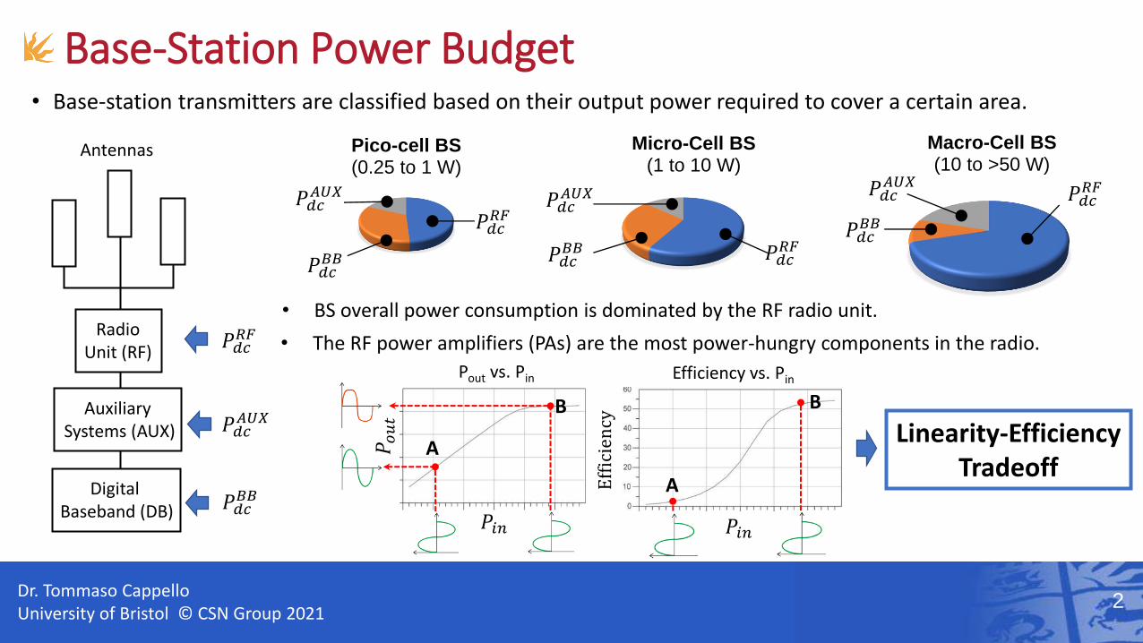
• Base-station transmitters are classified based on their output power required to cover a certain area.
2
RadioUnit (RF)
Antennas Macro-Cell BS(10 to >50 W)
𝑃𝑑𝑐𝐵𝐵
Pico-cell BS (0.25 to 1 W)
𝑃𝑑𝑐𝑅𝐹
𝑃𝑑𝑐𝐵𝐵
𝑃𝑑𝑐𝐴𝑈𝑋
Micro-Cell BS(1 to 10 W)
𝑃𝑑𝑐𝐵𝐵 𝑃𝑑𝑐
𝑅𝐹
𝑃𝑑𝑐𝐴𝑈𝑋 𝑃𝑑𝑐
𝐴𝑈𝑋𝑃𝑑𝑐𝑅𝐹
• BS overall power consumption is dominated by the RF radio unit.
Digital Baseband (DB)
Base-Station Power Budget
Auxiliary Systems (AUX) 𝑃𝑑𝑐
𝐴𝑈𝑋
𝑃𝑑𝑐𝐵𝐵
𝑃𝑑𝑐𝑅𝐹
A
B𝑃𝑜𝑢𝑡
𝑃𝑖𝑛 𝑃𝑖𝑛
Efficiency
A
B
Efficiency vs. PinPout vs. Pin
Linearity-EfficiencyTradeoff
• The RF power amplifiers (PAs) are the most power-hungry components in the radio.

Dr. Tommaso CappelloUniversity of Bristol © CSN Group 2021 3
Linearity Impairments in the Transmitter
Nonlinear compression, I/Q offset, LO leakage,…
Digital-to-Analog Converter
𝑓𝑐
Digital-to-Analog Converter
𝐼(𝑛)
PA BPF
𝑄 𝑛
INL/DNL distortion
Major source of nonlinear memory effects
Frequency Distortion
Bit Source
Modulation(BPSK, QPSK,…)
Parallelto
Serial
… … Crest Factor Reduction
IFFT
Serialto
Parallel
Cyclic Prefix
Nonlinear memory effects
Nonlinear memory effects
• Transmitter linearity and efficiency is limited by the RF frontend.
Output Spectrum
Input Spectrum
DriverD
Starting from 4G, RF hardware capabilities are becoming more and more a performance limitation
90°

Dr. Tommaso CappelloUniversity of Bristol © CSN Group 2021
[1] T. Cappello, Z. Popovic, K. Morris and A. Cappello, "Gaussian PulseCharacterization of RF Power Amplifiers," in IEEE Microwave andWireless Components Letters, April 2021.
LTE 1.4MHz signal partition
Gaussian pulse (FWHM = 930ns)
• Gaussian pulse decomposition is equivalent to the response with an LTE signal (not a-priori known).
• More powerful than the sinusoidal and time-domain techniques.
• Gaussian pulse is optimal for capturing NL memory effects.
0 250 500−500 −250
1
1
2
0 20MHz
Am
plit
ud
e
Time (ns)
4
• It is necessary to rethink the way transmitters are characterized → hybrid time-frequency characterization.
Gaussian decomposition [1]
Hybrid Time-Frequency Transmitter Characterization

Dr. Tommaso CappelloUniversity of Bristol © CSN Group 2021
5
[1] T. Cappello, C. Florian, A. Santarelli and Z. Popovic, "Linearization of a 500-W L-band GaN Doherty Power Amplifier by Dual-Pulse Trap Characterization26th May 2021," in IEEE Int’l Microw. Symp. (IMS), June 2019.
TPK-PK
EnvelopeBW
Gain w/o pre-pulse
𝜏𝑅
• GaN PAs, however, are still affected by trapping effects
VMAX
TPK-PK
Trap state (X)
… …
VMAX
DPD OFF
IdealDPD ON (𝑇𝑃𝐾−𝑃𝐾 < 𝜏𝑅)
DPD ON (𝑇𝑃𝐾−𝑃𝐾 > 𝜏𝑅)
• New finding [1]: If TPK-PK separation is longer than the dominating trap time constant (𝜏𝑅), a memory-less DPD is effective.
• This is particularly evident with high-PAPR signals (e.g., OFDM):
Pre-pulse Measure-pulse
X1(t)
Time TPK-PK0
X2(t)
X3(t)
X
PMAX
POUT
XMAX
• New characterization technique that mimics the envelope signal
• GaN is a candidate technology to improve the bandwidth/efficiency of RF frontends.
• Doherty architecture is common in macro-cell base-stations. GaN Doherty PA
Trapping Effects in GaN Doherty PAs
Dr. Tommaso CappelloUniversity of Bristol © CSN Group 2021
6
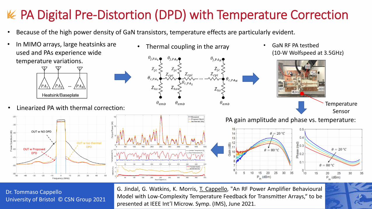
• In MIMO arrays, large heatsinks are used and PAs experience wide temperature variations.
• Thermal coupling in the array • GaN RF PA testbed (10-W Wolfspeed at 3.5GHz)
G. Jindal, G. Watkins, K. Morris, T. Cappello, "An RF Power Amplifier BehaviouralModel with Low-Complexity Temperature Feedback for Transmitter Arrays,“ to bepresented at IEEE Int’l Microw. Symp. (IMS), June 2021.
• Linearized PA with thermal correction:
PA gain amplitude and phase vs. temperature:
• Because of the high power density of GaN transistors, temperature effects are particularly evident.
TemperatureSensor
PA Digital Pre-Distortion (DPD) with Temperature Correction
Dr. Tommaso CappelloUniversity of Bristol © CSN Group 2021
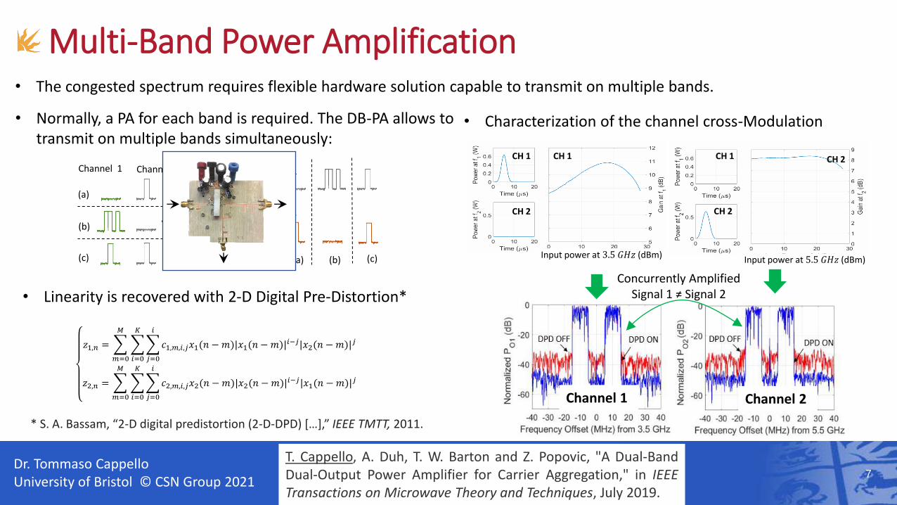
• The congested spectrum requires flexible hardware solution capable to transmit on multiple bands.
• Normally, a PA for each band is required. The DB-PA allows to transmit on multiple bands simultaneously:
T. Cappello, A. Duh, T. W. Barton and Z. Popovic, "A Dual-BandDual-Output Power Amplifier for Carrier Aggregation," in IEEETransactions on Microwave Theory and Techniques, July 2019.
𝑧1,𝑛 =
𝑚=0
𝑀
𝑖=0
𝐾
𝑗=0
𝑖
𝑐1,𝑚,𝑖,𝑗𝑥1(𝑛 − 𝑚)|𝑥1(𝑛 − 𝑚)|𝑖−𝑗|𝑥2(𝑛 − 𝑚)|𝑗
𝑧2,𝑛 =
𝑚=0
𝑀
𝑖=0
𝐾
𝑗=0
𝑖
𝑐2,𝑚,𝑖,𝑗𝑥2(𝑛 − 𝑚)|𝑥2(𝑛 − 𝑚)|𝑖−𝑗|𝑥1(𝑛 − 𝑚)|𝑗
• Linearity is recovered with 2-D Digital Pre-Distortion*
* S. A. Bassam, “2-D digital predistortion (2-D-DPD) […],” IEEE TMTT, 2011.
Input power at 3.5 𝐺𝐻𝑧 (dBm)Input power at 5.5 𝐺𝐻𝑧 (dBm)
• Characterization of the channel cross-Modulation
CH 1
CH 2
CH 1 CH 1 CH 2
CH 2
(a)
(a) (b) (c)
Channel 1
(b)
Channel 2
(c)
DB-PA
𝑃𝑂1
𝑃𝑂2
𝑃𝐼𝑁
Channel 1
Channel 2
Channel 1 Channel 2
Concurrently AmplifiedSignal 1 ≠ Signal 2
Multi-Band Power Amplification
7

Dr. Tommaso CappelloUniversity of Bristol © CSN Group 2021
Coupling
8
• MIMO is used for high-capacity data links and it requires an high number of antennas in small volume.
• Typical MIMO antenna array • Coupling (|S21|) between two nearby elements
AntennaS-parameters
PA1
PA2
• The PAs experience active load-pulling because of the coupling between the antenna elements [1].
[1] F. M. Barradas, P. M. Tomé, J. M. Gomes, T. R. Cunha, P. M. Cabral and J. C.
Pedro, "Power, Linearity, and Efficiency Prediction for MIMO Arrays With Antenna
Coupling," in IEEE Transactions on Microwave Theory and Techniques, Dec. 2017.
• Antenna coupling hardware simulator (most PAs are not available in simulators).
PA1
PA2
VariableAttenuator
VSG1
VSG2 VSA2
VSA1
• Synthesizable coupling factors (S21):
-12 dB↓
-21 dB @4.5GHz
-12 dB↓
-21 dB @1.5GHz
• PA gain variation for varying coupling:
PA1 PA2
CF (dB) = -21, -16, -12
Antenna Coupling in MIMO Arrays
Dr. Tommaso CappelloUniversity of Bristol © CSN Group 2021 9
S. Ozan, M. Nair, T. Cappello and M. A. Beach, "Low-Noise Amplifier withWideband Feedforward Linearisation for Mid-Band 5G Receivers," IEEEAsia Pacific Conference on Circuits and Systems (APCCAS), 2020.
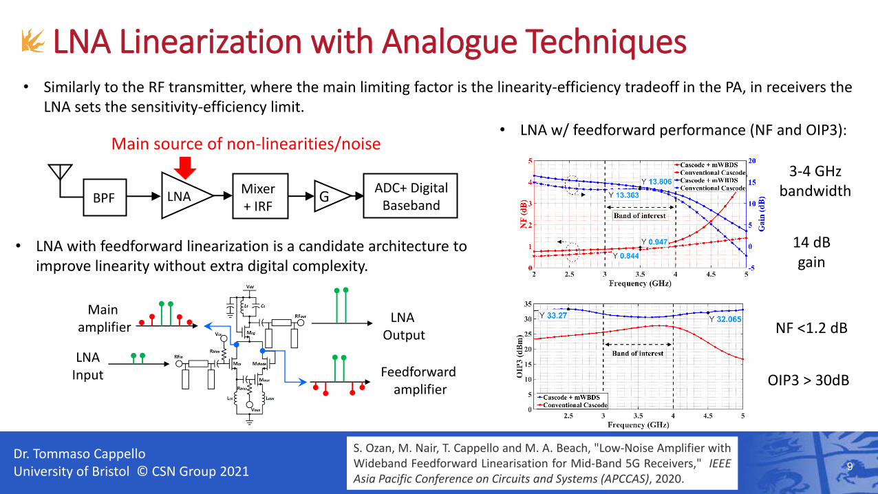
• Similarly to the RF transmitter, where the main limiting factor is the linearity-efficiency tradeoff in the PA, in receivers theLNA sets the sensitivity-efficiency limit.
• LNA with feedforward linearization is a candidate architecture to improve linearity without extra digital complexity.
• LNA w/ feedforward performance (NF and OIP3):
LNAMixer+ IRF
BPFADC+ Digital
BasebandG
Feedforward amplifier
Main amplifier
LNAOutput
LNAInput
Main source of non-linearities/noise
3-4 GHzbandwidth
14 dBgain
NF <1.2 dB
OIP3 > 30dB
LNA Linearization with Analogue Techniques

Dr. Tommaso CappelloUniversity of Bristol © CSN Group 2021
• When extra digital complexity can be afforded, digital post-distortion (DPOD) can be used to simplify the RF hardware.
10
LNA DPOD
STATIC LNACHARACTERISTIC
WIDEBANDCOMPENSATION
fLOW fHIGH
fLOW fHIGH
DPOD
LNA
DPOD
LNA
fLOW
fHIGH
fHIGH
fHIGH
fHIGHfLOW
• Wideband linearization can be achieved without the addition on noise by characterizing the LNA from fLOW to fHIGH.
• Digital complexity requirements and added power consumption need to be carefully investigated.
FPGA
A. Katz, J. Wood and D. Chokola, "The Evolution of PA Linearization:From Classic Feedforward and Feedback Through Analog and DigitalPredistortion," in IEEE Microwave Magazine, Feb. 2016.
LNA Linearization with Digital Techniques (DPD)
Dr. Tommaso CappelloUniversity of Bristol © CSN Group 2021
11
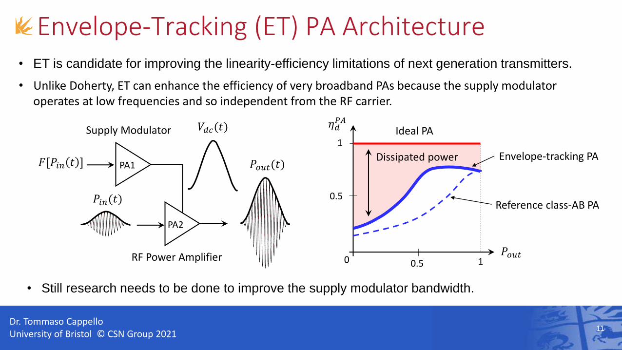
• ET is candidate for improving the linearity-efficiency limitations of next generation transmitters.
1
𝑃𝑜𝑢𝑡0
𝜂𝑑𝑃𝐴
0.5
Ideal PA
10.5
Reference class-AB PA
Dissipated power Envelope-tracking PAPA1
PA2
Supply Modulator
RF Power Amplifier
𝑃𝑜𝑢𝑡(𝑡)
𝑃𝑖𝑛(𝑡)
𝑉𝑑𝑐(𝑡)
𝐹[𝑃𝑖𝑛 𝑡 ]
Envelope-Tracking (ET) PA Architecture
• Still research needs to be done to improve the supply modulator bandwidth.
• Unlike Doherty, ET can enhance the efficiency of very broadband PAs because the supply modulator operates at low frequencies and so independent from the RF carrier.

Dr. Tommaso CappelloUniversity of Bristol © CSN Group 2021
12
• ET PAs are suitable for medium to high power PAs in the sub-6GHz spectrum.
• LTE compliant ET-PA @ 1.84GHz using the Power-DAC supply modulator [1].
[1] T. Cappello, P. Pednekar, C. Florian, S. Cripps, Z. Popovic and T. W. Barton, "Supply-and Load-Modulated Balanced Amplifier for Efficient Broadband 5G Base Stations,"in IEEE Transactions on Microwave Theory and Techniques, July 2019.
Vout
1
DCV = RV
2
2
DCV = RV
4
N
DCV = R
N
V
2
b1 b2 bNb1 b2 bN
2NL =( )3
1
1,02
Rout i O ii
i
VV b V b
=
= + =
…….
OV
• PA characteristics at variable supply level • FPGA DPD and ET control
Time (μs)
0 1 2 3 4 5 6 7 8 9 10
No
rmal
ized
Am
plit
ud
e
1
0.8
0.6
0.4
0.2
0
1
0.8
0.6
0.4
0.2
0
No
rmal
ized
Am
plit
ud
e
Vd
dD
ynam
ic B
ias
volt
age
(V)
30
20
10
0
Vd
d D
ynam
ic B
ias
volt
age
(V)30
20
10
0
ET no DPD
ET + DPD
In Env
Out Env
In Env
Out Env
NRMSE=27.8%
NRMSE = 4.2%
• LTE waveforms with and without DPD
ET-PA for Base-Station Transmitters (5G)
Dr. Tommaso CappelloUniversity of Bristol © CSN Group 2021
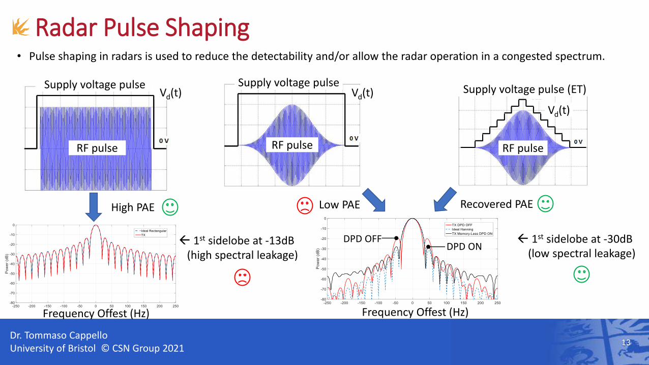
• Pulse shaping in radars is used to reduce the detectability and/or allow the radar operation in a congested spectrum.
13
Radar Pulse Shaping
RF pulse
Vd(t)
Supply voltage pulse (ET)
RF pulse
Vd(t)Supply voltage pulse
Vd(t)Supply voltage pulse
RF pulse
1st sidelobe at -13dB(high spectral leakage)
Frequency Offest (Hz)
1st sidelobe at -30dB(low spectral leakage)
High PAE Low PAE Recovered PAE
DPD ONDPD OFF
Frequency Offest (Hz)

Dr. Tommaso CappelloUniversity of Bristol © CSN Group 2021
14
ET for Radar Pulse Shaping• ET is an effective candidate to increase the efficiency of standalone or array PAs used with pulse-shaped waveforms.
• Typical and proposed way for PA supply
PACBS
CBank
ESRId
SW
VdPA
CBSVBUS
Id
Vd
Supply ModulatorVBUS
RF pulse input
RF pulse input
a. Rectangular supply voltage pulse
RF pulse output
RF pulse output
b. Shaped supply voltage pulse
• High-efficiency supply modulator
Po
we
r-D
AC
PA
• Integrated MMIC in Qorvo GaN 0.15μm [1]
𝑉𝐷𝐷2
𝑉𝐷𝐷4
𝑉𝐷𝐷2𝑁
PA
…
+-
+-
+-
𝑉𝑂𝑈𝑇 =
𝑖=1
𝑁
𝑏𝑖𝑉𝐷𝐷2𝑖
“Power-DAC”
• PA characterization and DPD
0 50 100 150 200 250 300-10
-5
0
5
10
15
20
25
30
35
40
Time (s)
Po
ut (d
Bm
)
PD
• Arbitrary radar pulses generation with high efficiency
T. Cappello, C. Florian, D. Niessen, R. P. Paganelli, S. Schafer and Z. Popovic, "Efficient X-Band Transmitter With Integrated GaN Power Amplifier and Supply Modulator," in IEEE Transactions on Microwave Theory and Techniques, April 2019.
65%45%49%52%

Dr. Tommaso CappelloUniversity of Bristol © CSN Group 2021
15
Conclusions & Take Aways• Since 4G, hardware performance are becoming more and more a limiting factor.
III-V semiconductor technologies (GaN/GaAs)
DPD-friendly RF hardware
RF architectures(multi-LNA, multi-PA, ET,…)
• Superior transceiver bandwidth, linearity, efficiency, noise figure, and operating frequencies compared to Silicon technologies.
• Most effective way to achieve large bandwidths and linearity.
• Reconfigurable and ‘upgradable’ RF hardware performance.
• Improve the single device technological limits by using multi-transistor architectures to achieve the required specifications.
Solutions to move forward:
Fundamental research is required to develop next generation RF transceivers

Dr. Tommaso CappelloUniversity of Bristol © CSN Group 2021
Active Circulator mm-Wave Front-Ends
• Magnetic circulators cannot be integrated in MMIC circuit operating at mmWaves.
16
L. Marzall, S. Verploegh, T. Cappello, M. Roberg and Z. Popović, "Active
MMIC Circulator Performance in a Phased-Array-Like Environment," 2020
50th European Microwave Conference (EuMC), 2021
• A possible alternative is to exploit the isolation introduced by transistors.
GaAs MMIC X-band
3dB gain Between 8-12GHz
7dB isolation over a very large bandwidth (simulation predicts >10dB)
Dr. Tommaso CappelloUniversity of Bristol © CSN Group 2021
17P. Zurek, T. Cappello and Z. Popovic, "Broadband Diplexed Power
Amplifier," in IEEE Microwave and Wireless Components Letters, Nov. 2020
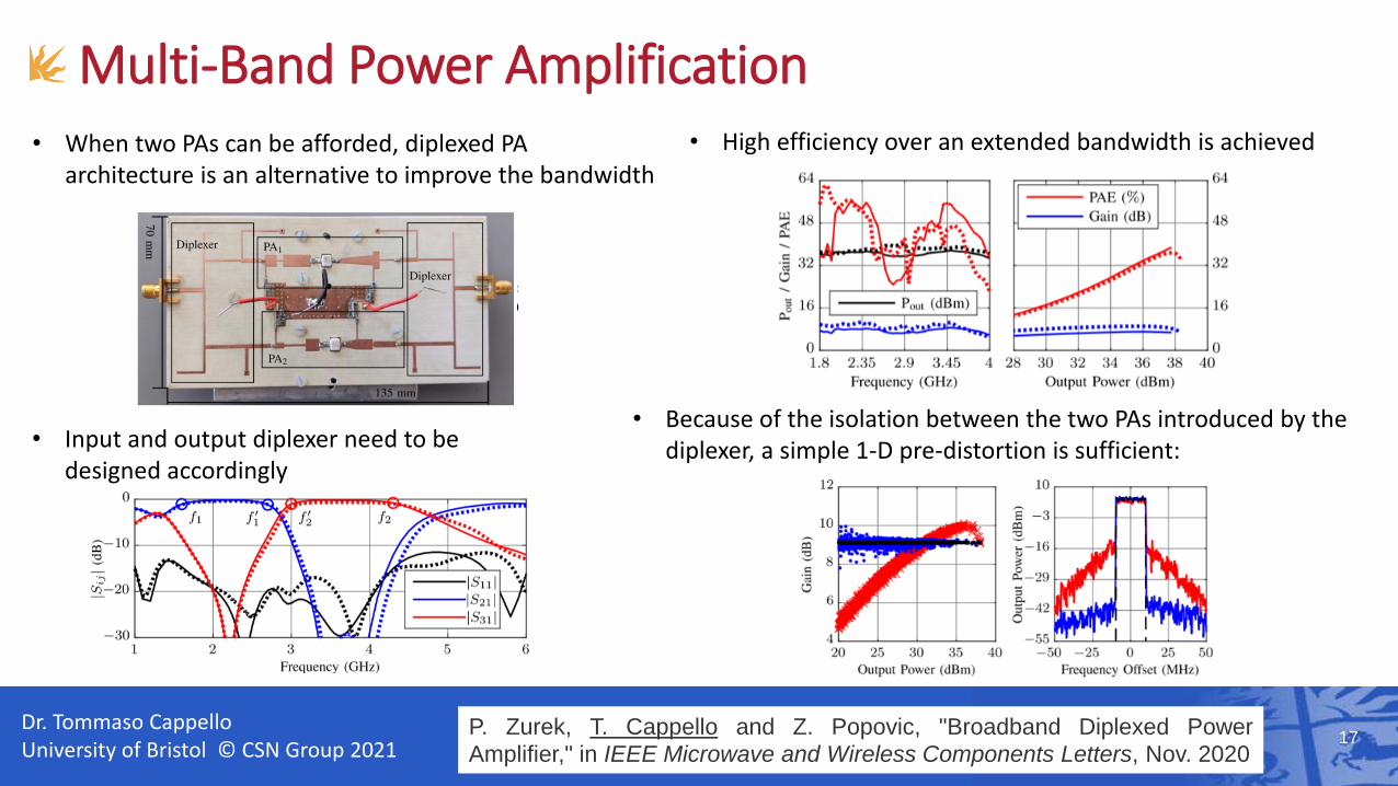
• When two PAs can be afforded, diplexed PA architecture is an alternative to improve the bandwidth
• Input and output diplexer need to be designed accordingly
• High efficiency over an extended bandwidth is achieved
• Because of the isolation between the two PAs introduced by the diplexer, a simple 1-D pre-distortion is sufficient:
Multi-Band Power Amplification

Dr. Tommaso CappelloUniversity of Bristol © CSN Group 2021
18
• With 5G, base-station PAs need to achieve wider bandwidths and efficiency with high PAPR signals.
• Solution: load-modulated balanced amplifier (LMBA) for bandwidth + ET for high PAPR [1]
[1] T. Cappello, P. Pednekar, C. Florian, S. Cripps, Z. Popovic and T. W. Barton,"Supply- and Load-Modulated Balanced Amplifier for Efficient Broadband 5G BaseStations," in IEEE Transactions on Microwave Theory and Techniques, July 2019.
• >20W between 1.8-3.8GHz with >40% average efficiency
CC
DF
• PAPRs 1-2dB higher than in LTE/LTE-A
2 GHz
140 MHz
• Record instantaneous bandwidth of 140MHz in ET mode
ET-PA for Base-Station Transmitters (5G)